CN111474465B - Flat-pack semiconductor device fixture and analysis method for EMMI analysis - Google Patents
Flat-pack semiconductor device fixture and analysis method for EMMI analysis Download PDFInfo
- Publication number
- CN111474465B CN111474465B CN202010341888.0A CN202010341888A CN111474465B CN 111474465 B CN111474465 B CN 111474465B CN 202010341888 A CN202010341888 A CN 202010341888A CN 111474465 B CN111474465 B CN 111474465B
- Authority
- CN
- China
- Prior art keywords
- semiconductor device
- flat
- analyzed
- base
- packaged semiconductor
- Prior art date
- Legal status (The legal status is an assumption and is not a legal conclusion. Google has not performed a legal analysis and makes no representation as to the accuracy of the status listed.)
- Active
Links
Images


Classifications
-
- G—PHYSICS
- G01—MEASURING; TESTING
- G01R—MEASURING ELECTRIC VARIABLES; MEASURING MAGNETIC VARIABLES
- G01R31/00—Arrangements for testing electric properties; Arrangements for locating electric faults; Arrangements for electrical testing characterised by what is being tested not provided for elsewhere
- G01R31/28—Testing of electronic circuits, e.g. by signal tracer
- G01R31/302—Contactless testing
- G01R31/308—Contactless testing using non-ionising electromagnetic radiation, e.g. optical radiation
- G01R31/311—Contactless testing using non-ionising electromagnetic radiation, e.g. optical radiation of integrated circuits
-
- G—PHYSICS
- G01—MEASURING; TESTING
- G01R—MEASURING ELECTRIC VARIABLES; MEASURING MAGNETIC VARIABLES
- G01R1/00—Details of instruments or arrangements of the types included in groups G01R5/00 - G01R13/00 and G01R31/00
- G01R1/02—General constructional details
- G01R1/04—Housings; Supporting members; Arrangements of terminals
- G01R1/0408—Test fixtures or contact fields; Connectors or connecting adaptors; Test clips; Test sockets
- G01R1/0425—Test clips, e.g. for IC's
Landscapes
- Engineering & Computer Science (AREA)
- Physics & Mathematics (AREA)
- General Physics & Mathematics (AREA)
- Computer Hardware Design (AREA)
- Microelectronics & Electronic Packaging (AREA)
- Health & Medical Sciences (AREA)
- Computer Vision & Pattern Recognition (AREA)
- Electromagnetism (AREA)
- Toxicology (AREA)
- General Engineering & Computer Science (AREA)
- Testing Of Individual Semiconductor Devices (AREA)
Abstract
本发明涉及用于EMMI分析的扁平封装半导体器件夹具及分析方法,夹具包括PCB基板、排针、底座、底座插针、簧片阵列、压杆和杆套;底座设置在PCB基板上;底座上设有两列所述簧片阵列;杆套设置在PCB基板上,压杆与杆套连接;待分析扁平封装半导体器件置于底座上,器件两侧的两管脚阵列分别与两列簧片阵列对接,压杆一端部紧压在器件的边框上,使器件管脚阵列与簧片阵列压紧连接;PCB基板上排布有微带引线,簧片阵列通过底座插针与微带引线连接,微带引线与排针连接。本发明的用于EMMI分析的扁平封装半导体器件夹具及分析方法,既能保证扁平封装半导体器件管脚与夹具良好连接,又能使扁平封装半导体器件的芯片充分暴露。

The invention relates to a flat package semiconductor device fixture for EMMI analysis and an analysis method. The fixture comprises a PCB substrate, a pin header, a base, a base pin, a reed array, a pressing rod and a rod sleeve; the base is arranged on the PCB substrate; There are two rows of the reed arrays; the rod sleeve is arranged on the PCB substrate, and the pressure rod is connected to the rod sleeve; the flat packaged semiconductor device to be analyzed is placed on the base, and the two pin arrays on both sides of the device are respectively connected with the two rows of reeds The array is docked, and one end of the pressing rod is pressed against the frame of the device, so that the pin array of the device is tightly connected with the reed array; the microstrip leads are arranged on the PCB substrate, and the reed array is connected with the microstrip leads through the base pins. , the microstrip lead is connected to the pin header. The flat-packaged semiconductor device fixture and the analysis method for EMMI analysis of the present invention can not only ensure good connection between the pins of the flat-packaged semiconductor device and the fixture, but also fully expose the chips of the flat-packaged semiconductor device.
Description
技术领域technical field
本发明涉及半导体测试分析技术领域,具体涉及一种用于EMMI分析的扁平封装半导体器件夹具及分析方法。The invention relates to the technical field of semiconductor testing and analysis, in particular to a flat package semiconductor device fixture for EMMI analysis and an analysis method.
背景技术Background technique
半导体材料中存在着多种载流子跃迁,包括带间跃迁、带隙内跃迁、缺陷能级跃迁等,除少数辐射跃迁外,其它跃迁都伴随着光子的产生。微光显微镜(EMMI)分析就是通过外置电场,收集样品辐射跃迁中产生的光子,以确定缺陷位置的技术。进行EMMI分析时,首先将失效半导体器件开封,而后在器件的异常管脚间加电并获取存在亮点的芯片EMMI图像,将失效器件和正常器件的芯片EMMI图像进行对比,失效器件芯片EMMI图像存在亮点而正常器件芯片EMMI图像不存在亮点的位置,往往就是存在失效缺陷的位置。由此可知,进行EMMI分析时,要保证半导体器件的芯片处于暴露状态。对于双列直插(DIP)等封装器件,将开封后的器件直接安装在相应的夹具上进行加电,即能完成EMMI分析。但对扁平封装半导体器件管脚加电,需通过夹具、PCB基板将扁平封装转换为DIP封装以方便进行加电测试,扁平封装半导体器件管脚与夹具是上下结构的电气连接,为使扁平封装半导体器件管脚与夹具能够良好连接,现有技术采取设置一个盖板压紧扁平封装半导体器件管脚与夹具,但盖板容易遮挡扁平封装半导体器件的芯片,导致无法针对器件进行EMMI分析。There are a variety of carrier transitions in semiconductor materials, including interband transitions, intrabandgap transitions, and defect level transitions. Except for a few radiative transitions, other transitions are accompanied by the generation of photons. Low-light microscopy (EMMI) analysis is a technique that uses an external electric field to collect photons generated in the radiation transition of the sample to determine the location of defects. When performing EMMI analysis, first unpack the failed semiconductor device, then power on the abnormal pins of the device and obtain the EMMI image of the chip with bright spots, and compare the chip EMMI image of the failed device and the normal device, and the EMMI image of the failed device chip exists. Bright spots and normal device chip EMMI images where there are no bright spots are often the locations where failure defects exist. It can be seen from this that when performing EMMI analysis, it is necessary to ensure that the chip of the semiconductor device is in an exposed state. For packaged devices such as dual in-line insertion (DIP), the EMMI analysis can be completed by directly installing the unsealed device on the corresponding fixture for power-on. However, to power on the pins of the flat packaged semiconductor device, it is necessary to convert the flat package into a DIP package through the fixture and PCB substrate to facilitate the power-on test. The pins of the flat packaged semiconductor device and the fixture are electrically connected with the upper and lower structures. The pins of the semiconductor device and the fixture can be well connected. In the prior art, a cover plate is used to press the pins and the fixture of the flat packaged semiconductor device, but the cover plate easily blocks the chip of the flat packaged semiconductor device, which makes it impossible to perform EMMI analysis on the device.
发明内容SUMMARY OF THE INVENTION
本发明的目的在于提供一种用于EMMI分析的扁平封装半导体器件夹具及分析方法,既能保证扁平封装半导体器件管脚与夹具良好连接,又能使扁平封装半导体器件的芯片充分暴露。The purpose of the present invention is to provide a flat package semiconductor device fixture and analysis method for EMMI analysis, which can not only ensure good connection between the pins of the flat package semiconductor device and the fixture, but also fully expose the chips of the flat package semiconductor device.
为了达到上述的目的,本发明提供一种用于EMMI分析的扁平封装半导体器件夹具,包括PCB基板、排针、底座、底座插针、簧片阵列、压杆和杆套;所述底座设置在所述PCB基板上;所述底座上设有两列所述簧片阵列;所述杆套设置在所述PCB基板上,所述压杆与所述杆套连接;待分析扁平封装半导体器件置于所述底座上,待分析扁平封装半导体器件两侧的两管脚阵列分别与两列所述簧片阵列对接,所述压杆一端部紧压在待分析扁平封装半导体器件的边框上,使待分析扁平封装半导体器件管脚阵列与所述簧片阵列压紧连接;所述PCB基板上排布有微带引线,所述簧片阵列通过所述底座插针与所述微带引线连接,所述微带引线与所述排针连接。In order to achieve the above-mentioned purpose, the present invention provides a flat package semiconductor device fixture for EMMI analysis, comprising a PCB substrate, a pin header, a base, a base pin, a reed array, a pressing rod and a rod sleeve; the base is arranged on the on the PCB substrate; the base is provided with two rows of the reed arrays; the rod sleeve is arranged on the PCB substrate, and the pressure rod is connected with the rod sleeve; the flat-packaged semiconductor device to be analyzed is installed. On the base, the two pin arrays on both sides of the flat-packaged semiconductor device to be analyzed are respectively butted with the two rows of the reed arrays, and one end of the pressing rod is pressed against the frame of the flat-packaged semiconductor device to be analyzed, so that the The pin array of the flat-packed semiconductor device to be analyzed is pressed and connected to the reed array; microstrip leads are arranged on the PCB substrate, and the reed array is connected to the microstrip lead through the base pins, The microstrip leads are connected to the pin headers.
上述用于EMMI分析的扁平封装半导体器件夹具,其中,所述杆套包括支柱和套筒,所述支柱一端固定在所述底座上,所述套筒固连在所述支柱另一端;所述套筒套在所述压杆上,所述压杆能相对所述套筒沿套筒轴线方向移动;所述套筒与所述支柱成一定角度,使所述压杆一端部能压向置于底座上的待分析扁平封装半导体器件。The above-mentioned flat package semiconductor device fixture for EMMI analysis, wherein the rod sleeve includes a pillar and a sleeve, one end of the pillar is fixed on the base, and the sleeve is fixed on the other end of the pillar; the The sleeve is sleeved on the pressing rod, and the pressing rod can move relative to the sleeve along the axis direction of the sleeve; the sleeve and the strut form a certain angle, so that one end of the pressing rod can be pressed toward the position A flat-pack semiconductor device to be analyzed on a submount.
上述用于EMMI分析的扁平封装半导体器件夹具,其中,所述杆套采用硬塑料制作;所述压杆具有一定弹性,所述压杆一端部设有压头,该压头紧压在待分析扁平封装半导体器件的边框上。The above-mentioned flat package semiconductor device fixture for EMMI analysis, wherein the rod sleeve is made of hard plastic; the pressure rod has a certain elasticity, and one end of the pressure rod is provided with an indenter, and the indenter is tightly pressed on the to-be-analyzed on the border of flat-pack semiconductor devices.
上述用于EMMI分析的扁平封装半导体器件夹具,其中,所述压杆设有压头的端部向下偏离水平方向20°。In the above-mentioned flat package semiconductor device fixture for EMMI analysis, wherein the end of the pressing rod provided with the pressing head deviates downward by 20° from the horizontal direction.
上述用于EMMI分析的扁平封装半导体器件夹具,其中,所述底座设有容置腔,两列所述簧片阵列置于该容置腔内。In the above-mentioned flat package semiconductor device fixture for EMMI analysis, wherein, the base is provided with an accommodating cavity, and the two rows of the reed arrays are placed in the accommodating cavity.
上述用于EMMI分析的扁平封装半导体器件夹具,其中,所述底座为矩形体;所述容置腔为矩形容置腔,该矩形容置腔外四个角处各设有一所述杆套和一所述压杆。The above-mentioned flat package semiconductor device fixture for EMMI analysis, wherein the base is a rectangular body; the accommodating cavity is a rectangular accommodating cavity, and the outer four corners of the rectangular accommodating cavity are respectively provided with the rod sleeve and the rod sleeve. a said pressure rod.
本发明还提供一种使用上述用于EMMI分析的扁平封装半导体器件夹具的EMMI分析方法,包括如下步骤:1)确定待分析扁平封装半导体器件的异常管脚;2)将待分析扁平封装半导体器件开封;3)安装待分析扁平封装半导体器件;4)根据待分析扁平封装半导体器件的异常管脚与排针的连接关系,设置合理的电压和电流,为排针加电;5)启动微光显微镜,通过微光显微镜获取待分析扁平封装半导体器件的EMMI图像,并拍照记录。The present invention also provides an EMMI analysis method using the above-mentioned flat-packaged semiconductor device fixture for EMMI analysis, comprising the following steps: 1) determining abnormal pins of the flat-packaged semiconductor device to be analyzed; 2) analyzing the flat-packaged semiconductor device to be analyzed Kaifeng; 3) Install the flat-packaged semiconductor device to be analyzed; 4) Set a reasonable voltage and current according to the connection relationship between the abnormal pins and pin headers of the flat-packaged semiconductor device to be analyzed; 5) Start the low light Microscope, the EMMI image of the flat-packaged semiconductor device to be analyzed is obtained by a low-light microscope, and the photograph is recorded.
与现有技术相比,本发明的有益技术效果是:Compared with the prior art, the beneficial technical effects of the present invention are:
1)扁平封装半导体器件安装在簧片阵列上后,可以调节压杆,使压杆压头刚好压在开封后器件边框上,能够压紧器件且不遮挡芯片,从而能够完成EMMI分析;所有管脚可以通过PCB基板上的排针引出,方便进行加电;1) After the flat package semiconductor device is installed on the reed array, the pressure rod can be adjusted so that the pressure rod indenter just presses on the device frame after unsealing, which can press the device without blocking the chip, so that the EMMI analysis can be completed; The pins can be drawn out through the pin headers on the PCB substrate, which is convenient for power-on;
2)本发明的用于EMMI分析的扁平封装半导体器件夹具,操作简单、成本低。2) The flat package semiconductor device fixture for EMMI analysis of the present invention has simple operation and low cost.
附图说明Description of drawings
本发明的用于EMMI分析的扁平封装半导体器件夹具及分析方法由以下的实施例及附图给出。The flat package semiconductor device fixture for EMMI analysis and the analysis method of the present invention are given by the following examples and accompanying drawings.
图1为本发明较佳实施例的用于EMMI分析的扁平封装半导体器件夹具的俯视图。1 is a top view of a flat-pack semiconductor device fixture for EMMI analysis according to a preferred embodiment of the present invention.
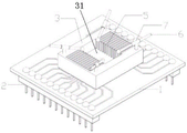
图2为本发明较佳实施例的用于EMMI分析的扁平封装半导体器件夹具的立体图。2 is a perspective view of a flat-pack semiconductor device fixture for EMMI analysis according to a preferred embodiment of the present invention.
图3为本发明较佳实施例的用于EMMI分析的扁平封装半导体器件夹具的剖面示意图。3 is a schematic cross-sectional view of a flat package semiconductor device fixture for EMMI analysis according to a preferred embodiment of the present invention.
具体实施方式Detailed ways
以下将结合图1~图3对本发明的用于EMMI分析的扁平封装半导体器件夹具及分析方法作进一步的详细描述。The flat package semiconductor device fixture for EMMI analysis and the analysis method of the present invention will be further described in detail below with reference to FIGS. 1 to 3 .
图1所示为本发明较佳实施例的用于EMMI分析的扁平封装半导体器件夹具的俯视图;图2所示为本发明较佳实施例的用于EMMI分析的扁平封装半导体器件夹具的立体图;图3所示为本发明较佳实施例的用于EMMI分析的扁平封装半导体器件夹具的剖面示意图。1 shows a top view of a flat package semiconductor device fixture for EMMI analysis according to a preferred embodiment of the present invention; FIG. 2 shows a perspective view of a flat package semiconductor device fixture for EMMI analysis according to a preferred embodiment of the present invention; 3 is a schematic cross-sectional view of a flat-pack semiconductor device fixture for EMMI analysis according to a preferred embodiment of the present invention.
参见图1至图3,本实施例的用于EMMI分析的扁平封装半导体器件夹具包括PCB基板1、排针2、底座3、底座插针4、簧片阵列5、压杆6和杆套7;Referring to FIG. 1 to FIG. 3 , the flat package semiconductor device fixture for EMMI analysis of this embodiment includes a PCB substrate 1 , a
所述底座3设置在所述PCB基板1上;The base 3 is arranged on the PCB substrate 1;
所述底座3上设有两列所述簧片阵列5,两列所述簧片阵列5分别与待分析扁平封装半导体器件两侧的两管脚阵列相匹配;The base 3 is provided with two rows of the
所述杆套7设置在所述PCB基板1上,所述压杆6与所述杆套7连接;待分析扁平封装半导体器件(开封后)置于所述底座3上,待分析扁平封装半导体器件两侧的两管脚阵列分别与两列所述簧片阵列5对接,所述压杆6一端部紧压在待分析扁平封装半导体器件的边框上,使待分析扁平封装半导体器件管脚阵列与所述簧片阵列5压紧连接,保证了待分析扁平封装半导体器件管脚阵列与夹具良好连接;The rod cover 7 is arranged on the PCB substrate 1, and the
所述PCB基板1上排布有微带引线8,所述簧片阵列5通过所述底座插针4与所述微带引线8连接,所述微带引线8与所述排针2连接;簧片阵列5、底座插针4、微带引线8和排针2将扁平封装转换为DIP封装,以方便进行加电测试。
本实施例的用于EMMI分析的扁平封装半导体器件夹具利用压杆6和杆套7的组合对待分析扁平封装半导体器件施加压紧力,保证待分析扁平封装半导体器件管脚阵列与夹具良好连接;施力由面(盖板)改为点(压杆6端部),避免了遮挡待分析扁平封装半导体器件的芯片,使加电测试中待分析扁平封装半导体器件的芯片充分暴露。The flat package semiconductor device fixture for EMMI analysis of this embodiment utilizes the combination of the
继续参见图1至图3,所述杆套7包括支柱和套筒,所述支柱一端固定在所述底座3上,所述套筒固连在所述支柱另一端;所述套筒套在所述压杆上,所述压杆可相对所述套筒沿套筒轴线方向移动;所述套筒与所述支柱成一定角度,使所述压杆6一端部能压向置于底座3上的待分析扁平封装半导体器件。Continuing to refer to FIGS. 1 to 3 , the rod sleeve 7 includes a strut and a sleeve, one end of the strut is fixed on the base 3 , and the sleeve is fixedly connected to the other end of the strut; the sleeve is sleeved on the base 3 . On the pressing rod, the pressing rod can move relative to the sleeve along the axis direction of the sleeve; the sleeve and the strut form a certain angle, so that one end of the
所述杆套7采用硬塑料制作;所述压杆6具有一定弹性,所述压杆6一端部设有压头,加电测试时该压头压在待分析扁平封装半导体器件的边框上。The rod cover 7 is made of hard plastic; the
所述压杆6与所述杆套7连接时,所述压杆6设有压头的端部向下偏离水平方向20°。When the
参见图2和图3,所述簧片阵列5由多片簧片等间距排列形成;一簧片阵列5中,簧片的数量、簧片的厚度以及相邻两簧片间的间距由待分析扁平封装半导体器件管脚阵列确定,应与待分析扁平封装半导体器件管脚阵列相匹配。对每一簧片配置一所述底座插针4。所述PCB基板1一表面排布有微带引线8,一条微带引线8对应一簧片,簧片通过其对应的底座插针4与其对应的微带引线8电连接。2 and 3, the
本实施例中,所述底座3为矩形体,在该矩形体四个角各设有一所述杆套7和一所述压杆6。In this embodiment, the base 3 is a rectangular body, and each of the four corners of the rectangular body is provided with a rod sleeve 7 and a
本实施例中,所述底座3设有容置腔31,两列所述簧片阵列5置于该容置腔31内,两列所述簧片阵列5之间的间距与待分析扁平封装半导体器件两列管脚阵列之间的间距相匹配。所述容置腔31为矩形容置腔31,所述杆套7位于所述容置腔31的外周,四个所述杆套7置于矩形容置腔31外的四个角处。In this embodiment, the base 3 is provided with an
参见图1和图2,所述PCB基板1上的多条微带引线8分布于所述底座3的两侧,同一侧的各微带引线8与同一簧片阵列5的各簧片连接。所述排针2包含两个,一个所述排针2对应一列所述簧片阵列5,同一侧的各微带引线8分别与同一排针2的各插针电连接。通过簧片、底座插针4、微带引线8和排针2的插针建立了待分析扁平封装半导体器件的管脚与排针2的插针一一对应关系。Referring to FIGS. 1 and 2 , a plurality of microstrip leads 8 on the PCB substrate 1 are distributed on both sides of the base 3 , and each
本实施例中,同一簧片阵列5包含12片簧片,同一簧片阵列5中相邻两簧片间的间距为5mm;底座插针4共24根,每一簧片阵列5分配12根;同一侧包含12条微带引线8,微带引线8采用宽度为20-24mil的走线;同一排针2包含12根插针,同一排针2中相邻两插针间的间距与标准双列直插管脚相匹配。In this embodiment, the
使用本实施例的用于EMMI分析的扁平封装半导体器件夹具进行EMMI分析包括如下步骤:Using the flat package semiconductor device fixture for EMMI analysis of this embodiment to perform EMMI analysis includes the following steps:
1)测试待分析扁平封装半导体器件(失效器件)各个管脚间的I-V特性,并与正常器件进行对比,确定异常管脚;1) Test the I-V characteristics between the pins of the flat-packaged semiconductor device (failed device) to be analyzed, and compare it with the normal device to determine the abnormal pins;
2)在不破坏待分析扁平封装半导体器件内部结构的情况下,将待分析扁平封装半导体器件开封;2) Unpack the flat-packaged semiconductor device to be analyzed without destroying the internal structure of the flat-packaged semiconductor device to be analyzed;
3)安装待分析扁平封装半导体器件;3) Install the flat-packaged semiconductor device to be analyzed;
将待分析扁平封装半导体器件置于底座3上,待分析扁平封装半导体器件两侧的两管脚阵列分别与两列簧片阵列5对接,待分析扁平封装半导体器件的管脚与簧片一一对应;移动四个压杆6,使压杆6的压头刚好压在开封后的待分析扁平封装半导体器件的边框上而不遮挡芯片;Place the flat-packaged semiconductor device to be analyzed on the base 3, the two pin arrays on both sides of the flat-packaged semiconductor device to be analyzed are respectively docked with two columns of
4)根据待分析扁平封装半导体器件的异常管脚与排针2的连接关系,设置合理的电压和电流,为排针2加电;4) According to the connection relationship between the abnormal pins of the flat-packaged semiconductor device to be analyzed and the
5)启动微光显微镜,通过微光显微镜获取待分析扁平封装半导体器件的EMMI图像,并拍照记录。5) Start the low-light microscope, acquire the EMMI image of the flat-packaged semiconductor device to be analyzed through the low-light microscope, and take pictures and record.
以上所述仅为本发明的优选实施例而已,并不用于限制本发明,对于本领域的技术人员来说,本发明可以有各种更改和变化。凡在本发明的精神和原则之内所作的任何更改、等同替换、改进等,均应包含在本发明的保护范围之内。The above descriptions are only preferred embodiments of the present invention, and are not intended to limit the present invention. For those skilled in the art, the present invention may have various modifications and changes. Any modification, equivalent replacement, improvement, etc. made within the spirit and principle of the present invention shall be included within the protection scope of the present invention.
Claims (10)
Priority Applications (1)
| Application Number | Priority Date | Filing Date | Title |
|---|---|---|---|
| CN202010341888.0A CN111474465B (en) | 2020-04-27 | 2020-04-27 | Flat-pack semiconductor device fixture and analysis method for EMMI analysis |
Applications Claiming Priority (1)
| Application Number | Priority Date | Filing Date | Title |
|---|---|---|---|
| CN202010341888.0A CN111474465B (en) | 2020-04-27 | 2020-04-27 | Flat-pack semiconductor device fixture and analysis method for EMMI analysis |
Publications (2)
| Publication Number | Publication Date |
|---|---|
| CN111474465A CN111474465A (en) | 2020-07-31 |
| CN111474465B true CN111474465B (en) | 2022-06-24 |
Family
ID=71755866
Family Applications (1)
| Application Number | Title | Priority Date | Filing Date |
|---|---|---|---|
| CN202010341888.0A Active CN111474465B (en) | 2020-04-27 | 2020-04-27 | Flat-pack semiconductor device fixture and analysis method for EMMI analysis |
Country Status (1)
| Country | Link |
|---|---|
| CN (1) | CN111474465B (en) |
Families Citing this family (2)
| Publication number | Priority date | Publication date | Assignee | Title |
|---|---|---|---|---|
| CN111999626A (en) * | 2020-08-02 | 2020-11-27 | 上海精密计量测试研究所 | Configurable I-V characteristic testing device and testing method thereof for semiconductor device |
| CN115206822B (en) * | 2022-06-23 | 2026-04-03 | 上海华虹宏力半导体制造有限公司 | Back-side wafer failure location fixture and method |
Citations (8)
| Publication number | Priority date | Publication date | Assignee | Title |
|---|---|---|---|---|
| JP2001344988A (en) * | 2000-05-30 | 2001-12-14 | Ricoh Co Ltd | Inspection method, apparatus, and image forming apparatus for semiconductor memory connection system |
| JP2003139816A (en) * | 2001-10-31 | 2003-05-14 | Koganei Corp | Contact unit |
| CN2916645Y (en) * | 2006-02-17 | 2007-06-27 | 原相科技股份有限公司 | Socket for testing image sensors |
| JP2007335605A (en) * | 2006-06-14 | 2007-12-27 | Renesas Technology Corp | Semiconductor failure analysis apparatus, failure analysis method, and failure analysis program |
| CN102074543A (en) * | 2009-11-20 | 2011-05-25 | 中芯国际集成电路制造(上海)有限公司 | Packaging pedestal for semiconductor |
| CN102116838A (en) * | 2010-01-05 | 2011-07-06 | 上海华虹Nec电子有限公司 | Emission microscope chip failure analyzing method and system |
| CN203117381U (en) * | 2012-12-07 | 2013-08-07 | 北京中微普业科技有限公司 | Testing device for radio frequency integrated circuit chip |
| CN105575987A (en) * | 2015-12-18 | 2016-05-11 | 积高电子(无锡)有限公司 | Packaging structure of image sensor and packaging technology |
Family Cites Families (1)
| Publication number | Priority date | Publication date | Assignee | Title |
|---|---|---|---|---|
| CN101063625B (en) * | 2006-04-30 | 2010-08-11 | 中芯国际集成电路制造(上海)有限公司 | BGA packaging retainer apparatus and method for testing BGA packaging |
-
2020
- 2020-04-27 CN CN202010341888.0A patent/CN111474465B/en active Active
Patent Citations (8)
| Publication number | Priority date | Publication date | Assignee | Title |
|---|---|---|---|---|
| JP2001344988A (en) * | 2000-05-30 | 2001-12-14 | Ricoh Co Ltd | Inspection method, apparatus, and image forming apparatus for semiconductor memory connection system |
| JP2003139816A (en) * | 2001-10-31 | 2003-05-14 | Koganei Corp | Contact unit |
| CN2916645Y (en) * | 2006-02-17 | 2007-06-27 | 原相科技股份有限公司 | Socket for testing image sensors |
| JP2007335605A (en) * | 2006-06-14 | 2007-12-27 | Renesas Technology Corp | Semiconductor failure analysis apparatus, failure analysis method, and failure analysis program |
| CN102074543A (en) * | 2009-11-20 | 2011-05-25 | 中芯国际集成电路制造(上海)有限公司 | Packaging pedestal for semiconductor |
| CN102116838A (en) * | 2010-01-05 | 2011-07-06 | 上海华虹Nec电子有限公司 | Emission microscope chip failure analyzing method and system |
| CN203117381U (en) * | 2012-12-07 | 2013-08-07 | 北京中微普业科技有限公司 | Testing device for radio frequency integrated circuit chip |
| CN105575987A (en) * | 2015-12-18 | 2016-05-11 | 积高电子(无锡)有限公司 | Packaging structure of image sensor and packaging technology |
Non-Patent Citations (2)
| Title |
|---|
| EMMI Failure-Distributed Analysis of ESD Zapping and Protection Designs in Power VDMOS ICs;Shen-Li Chen 等;《International Journal of Energy Science》;20140630;第4卷(第3期);第77-84页 * |
| 微光显微镜(EMMI)在器件失效分析中的应用;丁鸷敏 等;《电子显微学报》;20190430;第38卷(第2期);第156-158页 * |
Also Published As
| Publication number | Publication date |
|---|---|
| CN111474465A (en) | 2020-07-31 |
Similar Documents
| Publication | Publication Date | Title |
|---|---|---|
| US8912811B2 (en) | Test contact system for testing integrated circuits with packages having an array of signal and power contacts | |
| CN1103495C (en) | Testing apparatus for non-packaged semiconductor chip | |
| JP3690928B2 (en) | Carrier for testing unpackaged chips | |
| CN204989229U (en) | Chip test fixture and test system | |
| CN1226758A (en) | Integrated circuit socket for testing | |
| CN111474465B (en) | Flat-pack semiconductor device fixture and analysis method for EMMI analysis | |
| CN1334602A (en) | Semiconductor device and packaging method | |
| CN1662819A (en) | Test method for yielding a known good die | |
| CN1668931A (en) | Probe card for testing integrated circuits | |
| TW200924326A (en) | Socket and burn-in board provided with the socket | |
| JPWO2014041905A1 (en) | Test jig, inspection device, mounting device, and test device | |
| JP5491581B2 (en) | Socket for semiconductor chip inspection | |
| CN1355559A (en) | Wafer Test Carrier | |
| KR101790292B1 (en) | Cis probe card and the manufacturing method thereof | |
| JP2021107806A (en) | Press head lock mechanism, and electronic component inspection device with press head lock mechanism | |
| CN212675102U (en) | Flat-Pack Semiconductor Device Fixtures for EMMI Analysis | |
| CN205484687U (en) | General chip failure analysis's testing arrangement | |
| KR100659153B1 (en) | Insert for semiconductor package with support plate | |
| US7952186B2 (en) | Semiconductor package land grid array substrate and plurality of first and second electrodes | |
| JP2005539357A (en) | Die carrier | |
| CN219831172U (en) | A common fixture for testing and aging of micro chip components | |
| US5994910A (en) | Apparatus, and corresponding method, for stress testing wire bond-type semi-conductor chips | |
| US12578358B2 (en) | Socket board with a socket having heat conductive material disposed on bottom portion of the socket and method for inspecting a semiconductor device mounting in the socket | |
| US20250044351A1 (en) | Semiconductor test carrier, semiconductor test apparatus including the same, and semiconductor test method using semiconductor test apparatus | |
| US6888158B2 (en) | Bare chip carrier and method for manufacturing semiconductor device using the bare chip carrier |
Legal Events
| Date | Code | Title | Description |
|---|---|---|---|
| PB01 | Publication | ||
| PB01 | Publication | ||
| SE01 | Entry into force of request for substantive examination | ||
| SE01 | Entry into force of request for substantive examination | ||
| GR01 | Patent grant | ||
| GR01 | Patent grant | ||
| CP03 | Change of name, title or address | ||
| CP03 | Change of name, title or address |
Address after: 201109 Shanghai city Minhang District Yuanjiang Road No. 3888 Patentee after: Shanghai Institute of Aerospace Technology Country or region after: China Address before: 201109 Shanghai city Minhang District Yuanjiang Road No. 3888 Patentee before: SHANGHAI PRECISION METROLOGY AND TEST Research Institute Country or region before: China |