CN110709996A - Low leakage field effect transistor - Google Patents
Low leakage field effect transistor Download PDFInfo
- Publication number
- CN110709996A CN110709996A CN201880037789.4A CN201880037789A CN110709996A CN 110709996 A CN110709996 A CN 110709996A CN 201880037789 A CN201880037789 A CN 201880037789A CN 110709996 A CN110709996 A CN 110709996A
- Authority
- CN
- China
- Prior art keywords
- gate structure
- region
- edge
- work function
- regions
- Prior art date
- Legal status (The legal status is an assumption and is not a legal conclusion. Google has not performed a legal analysis and makes no representation as to the accuracy of the status listed.)
- Granted
Links
Images


Classifications
-
- H—ELECTRICITY
- H10—SEMICONDUCTOR DEVICES; ELECTRIC SOLID-STATE DEVICES NOT OTHERWISE PROVIDED FOR
- H10D—INORGANIC ELECTRIC SEMICONDUCTOR DEVICES
- H10D62/00—Semiconductor bodies, or regions thereof, of devices having potential barriers
- H10D62/10—Shapes, relative sizes or dispositions of the regions of the semiconductor bodies; Shapes of the semiconductor bodies
- H10D62/102—Constructional design considerations for preventing surface leakage or controlling electric field concentration
-
- H—ELECTRICITY
- H10—SEMICONDUCTOR DEVICES; ELECTRIC SOLID-STATE DEVICES NOT OTHERWISE PROVIDED FOR
- H10D—INORGANIC ELECTRIC SEMICONDUCTOR DEVICES
- H10D30/00—Field-effect transistors [FET]
- H10D30/60—Insulated-gate field-effect transistors [IGFET]
-
- H—ELECTRICITY
- H10—SEMICONDUCTOR DEVICES; ELECTRIC SOLID-STATE DEVICES NOT OTHERWISE PROVIDED FOR
- H10D—INORGANIC ELECTRIC SEMICONDUCTOR DEVICES
- H10D62/00—Semiconductor bodies, or regions thereof, of devices having potential barriers
- H10D62/10—Shapes, relative sizes or dispositions of the regions of the semiconductor bodies; Shapes of the semiconductor bodies
- H10D62/113—Isolations within a component, i.e. internal isolations
- H10D62/115—Dielectric isolations, e.g. air gaps
-
- H—ELECTRICITY
- H10—SEMICONDUCTOR DEVICES; ELECTRIC SOLID-STATE DEVICES NOT OTHERWISE PROVIDED FOR
- H10D—INORGANIC ELECTRIC SEMICONDUCTOR DEVICES
- H10D62/00—Semiconductor bodies, or regions thereof, of devices having potential barriers
- H10D62/10—Shapes, relative sizes or dispositions of the regions of the semiconductor bodies; Shapes of the semiconductor bodies
- H10D62/17—Semiconductor regions connected to electrodes not carrying current to be rectified, amplified or switched, e.g. channel regions
- H10D62/213—Channel regions of field-effect devices
- H10D62/221—Channel regions of field-effect devices of FETs
- H10D62/235—Channel regions of field-effect devices of FETs of IGFETs
- H10D62/299—Channel regions of field-effect devices of FETs of IGFETs having lateral doping variations
-
- H—ELECTRICITY
- H10—SEMICONDUCTOR DEVICES; ELECTRIC SOLID-STATE DEVICES NOT OTHERWISE PROVIDED FOR
- H10D—INORGANIC ELECTRIC SEMICONDUCTOR DEVICES
- H10D62/00—Semiconductor bodies, or regions thereof, of devices having potential barriers
- H10D62/60—Impurity distributions or concentrations
-
- H—ELECTRICITY
- H10—SEMICONDUCTOR DEVICES; ELECTRIC SOLID-STATE DEVICES NOT OTHERWISE PROVIDED FOR
- H10D—INORGANIC ELECTRIC SEMICONDUCTOR DEVICES
- H10D64/00—Electrodes of devices having potential barriers
- H10D64/01—Manufacture or treatment
- H10D64/017—Manufacture or treatment using dummy gates in processes wherein at least parts of the final gates are self-aligned to the dummy gates, i.e. replacement gate processes
-
- H—ELECTRICITY
- H10—SEMICONDUCTOR DEVICES; ELECTRIC SOLID-STATE DEVICES NOT OTHERWISE PROVIDED FOR
- H10D—INORGANIC ELECTRIC SEMICONDUCTOR DEVICES
- H10D64/00—Electrodes of devices having potential barriers
- H10D64/20—Electrodes characterised by their shapes, relative sizes or dispositions
- H10D64/27—Electrodes not carrying the current to be rectified, amplified, oscillated or switched, e.g. gates
- H10D64/311—Gate electrodes for field-effect devices
- H10D64/411—Gate electrodes for field-effect devices for FETs
- H10D64/511—Gate electrodes for field-effect devices for FETs for IGFETs
- H10D64/517—Gate electrodes for field-effect devices for FETs for IGFETs characterised by the conducting layers
- H10D64/519—Gate electrodes for field-effect devices for FETs for IGFETs characterised by the conducting layers characterised by their top-view geometrical layouts
-
- H—ELECTRICITY
- H10—SEMICONDUCTOR DEVICES; ELECTRIC SOLID-STATE DEVICES NOT OTHERWISE PROVIDED FOR
- H10D—INORGANIC ELECTRIC SEMICONDUCTOR DEVICES
- H10D64/00—Electrodes of devices having potential barriers
- H10D64/60—Electrodes characterised by their materials
- H10D64/66—Electrodes having a conductor capacitively coupled to a semiconductor by an insulator, e.g. MIS electrodes
- H10D64/661—Electrodes having a conductor capacitively coupled to a semiconductor by an insulator, e.g. MIS electrodes the conductor comprising a layer of silicon contacting the insulator, e.g. polysilicon having vertical doping variation
-
- H—ELECTRICITY
- H10—SEMICONDUCTOR DEVICES; ELECTRIC SOLID-STATE DEVICES NOT OTHERWISE PROVIDED FOR
- H10D—INORGANIC ELECTRIC SEMICONDUCTOR DEVICES
- H10D64/00—Electrodes of devices having potential barriers
- H10D64/60—Electrodes characterised by their materials
- H10D64/66—Electrodes having a conductor capacitively coupled to a semiconductor by an insulator, e.g. MIS electrodes
- H10D64/667—Electrodes having a conductor capacitively coupled to a semiconductor by an insulator, e.g. MIS electrodes the conductor comprising a layer of alloy material, compound material or organic material contacting the insulator, e.g. TiN workfunction layers
- H10D64/668—Electrodes having a conductor capacitively coupled to a semiconductor by an insulator, e.g. MIS electrodes the conductor comprising a layer of alloy material, compound material or organic material contacting the insulator, e.g. TiN workfunction layers the layer being a silicide, e.g. TiSi2
-
- H—ELECTRICITY
- H10—SEMICONDUCTOR DEVICES; ELECTRIC SOLID-STATE DEVICES NOT OTHERWISE PROVIDED FOR
- H10W—GENERIC PACKAGES, INTERCONNECTIONS, CONNECTORS OR OTHER CONSTRUCTIONAL DETAILS OF DEVICES COVERED BY CLASS H10
- H10W10/00—Isolation regions in semiconductor bodies between components of integrated devices
- H10W10/01—Manufacture or treatment
- H10W10/011—Manufacture or treatment of isolation regions comprising dielectric materials
- H10W10/012—Manufacture or treatment of isolation regions comprising dielectric materials using local oxidation of silicon [LOCOS]
-
- H—ELECTRICITY
- H10—SEMICONDUCTOR DEVICES; ELECTRIC SOLID-STATE DEVICES NOT OTHERWISE PROVIDED FOR
- H10W—GENERIC PACKAGES, INTERCONNECTIONS, CONNECTORS OR OTHER CONSTRUCTIONAL DETAILS OF DEVICES COVERED BY CLASS H10
- H10W10/00—Isolation regions in semiconductor bodies between components of integrated devices
- H10W10/10—Isolation regions comprising dielectric materials
- H10W10/13—Isolation regions comprising dielectric materials formed using local oxidation of silicon [LOCOS], e.g. sealed interface localised oxidation [SILO] or side-wall mask isolation [SWAMI]
Landscapes
- Thin Film Transistor (AREA)
- Metal-Oxide And Bipolar Metal-Oxide Semiconductor Integrated Circuits (AREA)
Abstract
Description
相关申请的交叉引用CROSS-REFERENCE TO RELATED APPLICATIONS
本申请要求于2017年6月7日提交的美国专利申请第15/616,811号的优先权,该美国专利申请的全部公开内容通过引用并入本文。This application claims priority to US Patent Application No. 15/616,811, filed June 7, 2017, the entire disclosure of which is incorporated herein by reference.
背景技术Background technique
(1)技术领域(1) Technical field
本发明涉及集成电路场效应晶体管(FET)设计,并且更具体地涉及低泄漏场效应晶体管设计。The present invention relates to integrated circuit field effect transistor (FET) designs, and more particularly to low leakage field effect transistor designs.
(2)背景技术(2) Background technology
在集成电路(IC)场效应晶体管(FET)的制造中,绝缘体上硅(SOI)衬底与体硅衬底相比具有许多益处,包括更高的速度、更低的功耗、改进的射频(RF)性能以及改进的辐射电阻。对于许多IC应用来说,介电隔离CMOS FET由于其可扩展性、低功率和设计灵活性而是优选的晶体管和逻辑结构。在介电隔离的CMOS中,N型MOSFET和P型MOSFET通过各自制造在其自己的硅岛中而彼此横向隔离。典型地这种隔离通过将SOI衬底的硅膜蚀刻成间隔开的岛并且用沉积的二氧化硅(SiO2)回填这些岛之间的间隙来提供,尽管在SOI的早期,通过晶体管之间硅区的局部氧化进行的隔离(也被称为LOCOS隔离)已经被广泛使用。In the manufacture of integrated circuit (IC) field effect transistors (FETs), silicon-on-insulator (SOI) substrates offer many benefits over bulk silicon substrates, including higher speed, lower power consumption, improved radio frequency (RF) performance and improved radiation resistance. For many IC applications, dielectrically isolated CMOS FETs are the preferred transistor and logic structures due to their scalability, low power, and design flexibility. In dielectrically isolated CMOS, N-type MOSFETs and P-type MOSFETs are laterally isolated from each other by each being fabricated in its own silicon island. Typically this isolation is provided by etching the silicon film of the SOI substrate into spaced apart islands and backfilling the gaps between these islands with deposited silicon dioxide ( SiO2 ), although in the early days of SOI, through transistors Isolation by local oxidation of silicon regions (also known as LOCOS isolation) has been widely used.
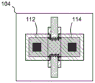
图1是在SOI上制造的典型的现有技术N型MOSFET(“nFET”)100的布局的顶视图。P型硅岛102以常规方式(例如,通过硼的扩散)形成在SOI衬底上,并且通过回填或LOCOS隔离被SiO2 104包围。在硅岛102上方形成包括绝缘体(例如,氧化物层)和上覆栅极材料(例如,多晶硅)的、具有长度L的栅极结构106。通过在硅岛102上方的掩膜注入区域111内注入或扩散N+材料(例如,磷,砷)来形成N型源极108区和N型漏极110区(注意,用于限定源极108N+注入区和漏极110N+注入区的掩膜注入区域111与围绕硅岛102的SiO2交叠)。因此,栅极结构106相对于源极108区和漏极110区是自对准的并且限定了源极108区与漏极110区之间的传导沟道113。分别对源极108区和漏极110区形成导电接触部112、114。为了清楚起见,省略了其他共同结构(例如,器件互连、栅极接触部等)。1 is a top view of the layout of a typical prior art N-type MOSFET ("nFET") 100 fabricated on SOI. P-
SiO2回填和LOCOS隔离技术以及类似的工艺使nFET传导沟道113的两个相对的横向边缘116(由参考椭圆118内的粗线指示)与SiO2接触(nFET 100的宽度垂直于长度L并且在SOI衬底的平面中)。在针对nFET100的IC制造处理期间,注入至栅极结构106下面的P型硅岛102内(即,FET传导沟道113内)的硼从nFET传导沟道113的边缘116处的硅中分离到相邻的SiO2 104中。分离使FET的边缘116处的硅中的硼浓度低于传导沟道113的中央区的硼浓度(该中央区大致由虚线参考框120包围)。众所周知,nFET 100的边缘116处的硼耗尽会导致沟道边缘处的阈值电压由于边缘116处的带隙向下弯曲而降低,典型地降低了十分之几伏(用于参考,硅的带隙为约1V)。对于每67mV的能带弯曲,漏极漏电流IdOFF约以十倍电流的速率增加。因此,与没有硼耗尽的平坦轮廓相比,nFET 100的边缘116处的硼耗尽可能使得边缘116处的漏电流增加多个数量级。 SiO2 backfill and LOCOS isolation techniques and similar processes bring the two opposing
这种现象自从SOI最早用于衬底以来就已经知道并且导致nFET 100的边缘116——所谓的“边缘晶体管”——处的较低阈值电压Vt,从而增加了漏电流(特别地因为每个晶体管典型地有两个边缘,如图1所示)。实际上,从这个角度来看,nFET 100可以被建模为三个并联的晶体管,具有阈值电压VtC的中央传导沟道晶体管和具有较低阈值电压VtE的两个边缘晶体管。由于其较低的VtE,两个边缘晶体管在中央传导沟道晶体管的VtC达到之前开始传导,导致边缘处泄漏增加。这种边缘泄漏通常会影响每个nFET的总泄漏,这转而可能使这种FET的待机功耗增加一个数量级或更多个数量级,并且因此增加使用这种nFET的任何系统的总功耗。这种边缘泄漏问题也可以在薄SOI衬底上制造的PMOSFET(“pFET”)中看到。This phenomenon has been known since SOI was first used for substrates and results in a lower threshold voltage Vt at the
虽然nFET的边缘晶体管的范围涉及nFET 100的边缘116处的栅极结构的长度以及沿该长度的掺杂浓度和在这些边缘处渗透至nFET的宽度(即,横向)和深度的程度,但是方便的是仅将边缘116称为边缘晶体管。因此,出于本公开内容的目的,除非另外表征,否则图1中由粗线指示的边缘116可以被认为限定所示的nFET 100的边缘晶体管。While the extent of the edge transistors of an nFET relates to the length of the gate structure at the
已经尝试通过增加nFET 100的边缘晶体管116处的栅极结构106的长度从而使nFET 100的相应边缘晶体管相对于nFET 100的中心区的长度L延长以及/或者通过将主沟道的边缘晶体管116从硅岛102后移来减少边缘晶体管泄漏。然而,这些方法具有许多缺点特别是在小宽度晶体管中具有许多缺点,包括不充分的漏电流减小、面积和总栅极电容的一定程度的增加和驱动电流ION的减小。Attempts have been made to lengthen the length L of the corresponding edge transistors of the
因此,存在对于在存在上述边缘晶体管现象的情况下呈现低泄漏的低泄漏FET设计的需要,并且特别地存在对于在SOI上制造的nFET的需要。Accordingly, there is a need for low leakage FET designs that exhibit low leakage in the presence of the edge transistor phenomenon described above, and in particular for nFETs fabricated on SOI.
发明内容SUMMARY OF THE INVENTION
本发明涵盖在存在边缘晶体管现象的情况下呈现低泄漏的FET设计,并且特别地涵盖在SOI上制造的NMOSFET(“nFET”)设计。本发明的实施方式包括nFET设计,其中通过改变覆盖在边缘晶体管的栅极结构的功函数来增加边缘晶体管的Vt(VtE)。为了描述本发明的实施方式,使用多晶硅栅极结构作为示例,但是可以使用其他栅极材料并且可以使用其他阈值改变技术以实现本发明。更具体地,本发明的一些实施方式通过在覆盖在边缘晶体管上的栅极多晶硅结构的至少一部分内形成额外P+注入区来增加nFET的覆盖在边缘晶体管上的栅极结构的功函数,从而将边缘晶体管的Vt增加至nFET的中央传导沟道的Vt并且可以超过nFET的中央传导沟道的Vt。The present invention encompasses FET designs that exhibit low leakage in the presence of edge transistor phenomena, and in particular NMOSFET ("nFET") designs fabricated on SOI. Embodiments of the invention include nFET designs in which the Vt (Vt E ) of an edge transistor is increased by changing the work function of the gate structure overlying the edge transistor. To describe embodiments of the present invention, a polysilicon gate structure is used as an example, but other gate materials may be used and other threshold changing techniques may be used to implement the present invention. More specifically, some embodiments of the present invention increase the work function of the gate structure overlying the edge transistor by forming an additional P+ implant region within at least a portion of the gate polysilicon structure overlying the edge transistor, thereby increasing the work function of the gate structure overlying the edge transistor. The Vt of the edge transistor increases to the Vt of the nFET's center conduction channel and can exceed the Vt of the nFET's center conduction channel.
在变型实施方式中,nFET的覆盖在边缘晶体管上的栅极结构的功函数可以通过以下方式增加:创建混合多晶硅/金属栅极结构,其中多晶硅在中央区并且金属或类金属材料在栅极结构的边缘区上方;创建在栅极结构的中央区和边缘区中具有两种不同的金属或类金属材料的栅极结构;创建共掺杂有N+掺杂物和P+掺杂物两者的栅极结构,以创建在栅极结构的边缘区上方的简并掺杂的多晶硅,使得功函数在栅极结构的中央区与边缘区之间不同;并且在栅极结构下方掺杂绝缘体使得功函数在栅极结构的中央区与边缘区之间不同。In variant embodiments, the work function of the gate structures of the nFETs overlying the edge transistors can be increased by creating a hybrid poly/metal gate structure with poly in the central region and metal or metal-like material in the gate structure over the edge region of the gate structure; create a gate structure with two different metals or metal-like materials in the central and edge regions of the gate structure; create a gate co-doped with both N+ and P+ dopants pole structure to create degenerate doped polysilicon over the edge region of the gate structure such that the work function differs between the central and edge regions of the gate structure; and doping the insulator under the gate structure such that the work function It differs between the central region and the edge region of the gate structure.
另外,在一些实施方式中,还修改了nFET的栅极结构以使边缘晶体管的有效沟道长度相对于FET的中央传导沟道的长度增加或“扩展”。除了由于功函数修改而减小的漏电流以外,增加的边缘晶体管沟道长度致使漏电流的进一步减小,更接近地近似nFET的中央传导沟道的漏电流IdOFF。Additionally, in some embodiments, the gate structure of the nFET is also modified to increase or "spread" the effective channel length of the edge transistors relative to the length of the center conduction channel of the FET. In addition to the reduced leakage current due to work function modification, the increased edge transistor channel length results in a further reduction in leakage current, more closely approximating the leakage current IdOFF of the center conduction channel of the nFET.
本发明的一个或更多个实施方式的细节在附图和下面的描述中进行阐述。根据说明书和附图并且根据权利要求书,本发明的其他特征、目的和优点将变得明显。The details of one or more embodiments of the invention are set forth in the accompanying drawings and the description below. Other features, objects and advantages of the present invention will become apparent from the description and drawings, and from the claims.
附图说明Description of drawings
图1是在SOI上制造的典型的现有技术N型MOSFET(“nFET”)的布局的顶视图。Figure 1 is a top view of the layout of a typical prior art N-type MOSFET ("nFET") fabricated on SOI.
图2A是在SOI上制造并且掺杂有额外P+注入区的nFET的第一实施方式的布局的顶视图。2A is a top view of the layout of a first embodiment of an nFET fabricated on SOI and doped with additional P+ implant regions.
图2B是针对图2A的实施方式的掩膜注入区域(尺寸减小)的布局的顶视图。Figure 2B is a top view of the layout of the mask implant region (reduced size) for the embodiment of Figure 2A.
图3是在SOI上制造并且掺杂有额外P+注入区的nFET的第二实施方式的布局的顶视图。3 is a top view of the layout of a second embodiment of an nFET fabricated on SOI and doped with additional P+ implant regions.
图4A是在SOI上制造并且掺杂有额外P+注入区的nFET的第三实施方式的布局的顶视图。4A is a top view of the layout of a third embodiment of an nFET fabricated on SOI and doped with additional P+ implant regions.
图4B是针对图4A的实施方式的掩膜注入区域(尺寸减小)的布局的顶视图。4B is a top view of the layout of the mask implant region (reduced size) for the embodiment of FIG. 4A.
图5A至图5E是针对图2A的nFET的示例性制造顺序的顶视图。5A-5E are top views of an exemplary fabrication sequence for the nFET of FIG. 2A.
图6A至图6E是针对图4A的nFET的示例性制造顺序的顶视图。6A-6E are top views of an exemplary fabrication sequence for the nFET of FIG. 4A.
图7是在SOI上制造的、掺杂有额外P+注入区并且被配置用于本体连结的nFET的第四实施方式的布局的顶视图。7 is a top view of the layout of a fourth embodiment of an nFET fabricated on SOI, doped with additional P+ implant regions, and configured for body bonding.
图8是部分完成的具有覆盖被SiO2包围的P型硅岛的双金属栅极的nFET的顶视图。Figure 8 is a top view of a partially completed nFET with dual metal gates covering P-type silicon islands surrounded by SiO2 .
图9是示出用于在绝缘体上硅衬底上制造FET的方法的过程流程图。9 is a process flow diagram illustrating a method for fabricating a FET on a silicon-on-insulator substrate.
图10是示出用于在绝缘体上硅衬底上制造NMOSFET的方法的过程流程图。10 is a process flow diagram illustrating a method for fabricating an NMOSFET on a silicon-on-insulator substrate.
在各个附图中相似的附图标记和名称指示相似的元件。Like numerals and names indicate like elements throughout the various figures.
具体实施方式Detailed ways
概述Overview
本发明涵盖在存在边缘晶体管现象的情况下呈现低泄漏的FET设计,并且特别地涵盖在SOI上制造的NMOSFET(“nFET”)设计。本发明的实施方式包括nFET设计,其中通过改变覆盖在边缘晶体管上的栅极结构的功函数来增加边缘晶体管的Vt。为了描述本发明的实施方式,使用多晶硅栅极结构作为示例,但是可以使用其他栅极材料并且可以使用其他阈值改变技术来实现本发明。更具体地,本发明的一些实施方式通过在覆盖在边缘晶体管上的栅极多晶硅结构的至少一部分内形成额外P+注入区来增加nFET的覆盖在边缘晶体管上的栅极结构的功函数,从而将边缘晶体管的Vt(VtE)增加至至少等于nFET的中央传导沟道的Vt(VtC)的水平,并且可以超过nFET的中央传导沟道的Vt(VtC)。The present invention encompasses FET designs that exhibit low leakage in the presence of edge transistor phenomena, and in particular NMOSFET ("nFET") designs fabricated on SOI. Embodiments of the invention include nFET designs in which the Vt of the edge transistor is increased by changing the work function of the gate structure overlying the edge transistor. To describe embodiments of the present invention, a polysilicon gate structure is used as an example, but other gate materials may be used and other threshold changing techniques may be used to implement the present invention. More specifically, some embodiments of the present invention increase the work function of the gate structure overlying the edge transistor by forming an additional P+ implant region within at least a portion of the gate polysilicon structure overlying the edge transistor, thereby increasing the work function of the gate structure overlying the edge transistor. The Vt (Vt E ) of the edge transistor increases to a level at least equal to the Vt (Vt C ) of the center conduction channel of the nFET, and may exceed the Vt (Vt C ) of the center conduction channel of the nFET.
如本领域中已知的,nFET的Vt由若干个主要因素确定,其中最重要的是沟道掺杂浓度NA、栅极结构的功函数ΦMF和栅极氧化物厚度tOX。增加ΦMF、NA或tOX中的任意一个都会使Vt增加。然而,改变沟道掺杂浓度NA和栅极氧化物厚度tOX可能影响nFET的其他性能设计参数,特别是对数字晶体管和模拟晶体管的电路速度有很大的影响的饱和漏极电流Idsat。因此,本发明的实施方式增加nFET的覆盖在边缘晶体管上的栅极结构的ΦMF,优选地通过在覆盖在边缘晶体管上的栅极结构的至少一部分内形成额外P+注入区来增加,从而使边缘晶体管的阈值电压VtE增加。As known in the art, the Vt of an nFET is determined by several major factors, the most important of which are the channel doping concentration NA , the work function Φ MF of the gate structure, and the gate oxide thickness t OX . Increasing any of Φ MF , NA or t OX will increase Vt. However, changing the channel doping concentration NA and gate oxide thickness tOX may affect other performance design parameters of the nFET, especially the saturation drain current Idsat which has a large effect on the circuit speed of digital and analog transistors. Accordingly, embodiments of the present invention increase the Φ MF of the gate structure overlying the edge transistor of the nFET, preferably by forming additional P+ implant regions within at least a portion of the gate structure overlying the edge transistor, thereby enabling The threshold voltage Vt E of the edge transistor increases.
这种nFET设计的变型实施方式还“扩展”覆盖在边缘晶体管上的栅极结构以使边缘晶体管的有效沟道长度相对于nFET的中央传导沟道的长度增加。除了由于栅极功函数修改而引起的漏电流减小以外,增加的边缘晶体管沟道长度使得漏电流进一步减小,更接近地近似nFET的中央传导沟道的漏电流IdOFF。This variant embodiment of the nFET design also "extends" the gate structure overlying the edge transistors so that the effective channel length of the edge transistors is increased relative to the length of the center conduction channel of the nFET. In addition to the reduction in leakage current due to gate work function modification, the increased edge transistor channel length results in a further reduction in leakage current, more closely approximating the leakage current Id OFF of the center conduction channel of the nFET.
下面描述的本公开内容的附图示出了增强型nFET,在该增强型nFET中,源极区和漏极区为N+、传导沟道为P型、栅极结构为N+多晶硅(优选地具有硅化物层以减小栅极电阻)、并且本体连结——若存在——具有P+接触区以与到NMOSFET的浮动P型本体的P型本体连结连接接触。然而,在一些应用中,本发明的教导可以适用于pFET和耗尽型FET。例如,使用薄绝缘体上硅衬底制造IC可能导致pFET在其边缘晶体管处泄漏;可以使用下面描述的方法通过反掺杂(例如,多晶硅栅极结构上的N+注入)来制造低泄露pFET。因此,所示出的实施方式和示例性材料不应当被视为对本发明内容的范围的限制。The figures of the present disclosure described below show an enhancement mode nFET in which the source and drain regions are N+, the conduction channel is P-type, and the gate structure is N+ polysilicon (preferably with silicide layer to reduce gate resistance), and the body bond, if present, has a P+ contact region to make contact with the P-type body bond connection to the floating P-type body of the NMOSFET. However, in some applications, the teachings of the present invention may be applicable to pFETs and depletion FETs. For example, using thin silicon-on-insulator substrates to fabricate ICs can result in pFETs leaking at their edge transistors; low-leakage pFETs can be fabricated by counter-doping (eg, N+ implants on polysilicon gate structures) using the methods described below. Accordingly, the illustrated embodiments and exemplary materials should not be construed as limiting the scope of the present disclosure.
作为进一步的背景技术,在于1999年1月26日授予的题为“Self-Aligned EdgeControl in Silicon on Insulator”的美国专利第5,863,823号中阐述了FET制造的若干种方法的细节,该美国专利转让给本发明的受让人,其全部内容通过引用并入本文。As further background, details of several methods of FET fabrication are set forth in US Patent No. 5,863,823, entitled "Self-Aligned EdgeControl in Silicon on Insulator," issued January 26, 1999, assigned to assignee of the present invention, the entire contents of which are incorporated herein by reference.
示例性实施方式-ΦMF修改Exemplary Embodiment - Φ MF Modification
图2A是在SOI上制造并且掺杂有额外P+注入区的nFET 200的第一实施方式的布局的顶视图。如图1所示,P型硅岛102以常规方式(例如,通过硼的扩散)形成在SOI衬底上并且被SiO2 104包围(例如,通过回填或LOCOS隔离)。在硅岛102上形成包括绝缘体(例如,氧化物层)和上覆栅极材料(例如,多晶硅)的栅极结构106。通过常规手段在与硅岛102交叠的掩膜注入区域211内形成N型源极108区和N型漏极110区。图2B是针对图2A的实施方式的掩膜注入区域211(尺寸减小)的布局的顶视图。2A is a top view of the layout of a first embodiment of an
栅极结构106相对于源极108区和漏极110区是自对准的并且限定了源极108区与漏极110区之间的传导沟道113。分别对源极108区和漏极110区形成导电接触部112、114。为了清楚起见,省略了其他共同结构(例如,器件互连、栅极接触部等)。如本领域中已知的,可以采取附加步骤以创建用于特定应用的特征和结构(例如,用于控制或塑造耗尽区的范围的晕圈区(halo region)、轻掺杂漏极(LDD)区、偏移间隔物等),并且每个单独的nFET 200通常将连接至同一衬底上的其他有源电路元件和无源电路元件。另外参见图5A至图5E的针对图2A的nFET 200的示例性制造顺序的视图。The
如通过比较图1与图2A应当清楚的,并且特别地通过图2B应当清楚的,用于限定图2A中的nFET 200的源极108N+注入区和漏极110N+注入区的掩膜注入区域211与用于限定图1中的nFET 100的源极108N+注入区和漏极110N+注入区的矩形掩膜注入区域111在形状上不同。更具体地,图2A的掩膜注入区域211的边缘在边缘晶体管116上方的两侧上被刻有切口,如由粗虚线206所指示的,以避免在nFET 200的边缘晶体管116的大部分或全部上方注入N+材料;该切口在图2B中是明显的。As should be apparent by comparing Figure 1 with Figure 2A, and particularly by Figure 2B, the
本发明的重要方面在于,改变覆盖在边缘晶体管116上的栅极结构106以通过改变栅极结构106的部分的功函数来使边缘晶体管的Vt增加。更具体地,在栅极结构106的至少一部分内且在边缘晶体管116的一部分上方(该部分以虚线示出)形成额外P+注入区208、210。P+注入区208、210通常被配置成仅影响栅极结构106的在边缘晶体管116上方的部分,而不影响栅极结构106的中央部分。如所指示的,P+注入区208、210的长度LP通常应当小于或等于栅极结构106的中心处的长度L,以避免P+掺杂物注入到nFET 200的源极108区和漏极110区。保持LP<L在P+注入区208、210的两侧提供对准缓冲区。应当理解的是,P+注入区208、210成为栅极结构106的组成部分,而不仅仅是增加的材料层。An important aspect of the present invention is that the
在变型实施方式中,P+注入区208、210可以与用于源极108和漏极110的N+注入区交叠。这种交叠将在栅极结构106的一部分内形成简并掺杂的多晶硅;然而,这种结构仍将具有比纯N+区更高的阈值电压。这种配置在对准公差使得一些nFET器件可以具有N+/P+交叠区的情况下可能是有用的。In variant embodiments, the P+ implanted
通过在边缘晶体管116的一部分上方的栅极结构106的至少一部分内形成P+注入区208、210,栅极结构106的注入部分的ΦMF增加。如本领域普通技术人员将理解的,可以选择P+掺杂的量(例如,通过建模和/或实验)以使边缘晶体管116的VtE与nFET 200的中央传导沟道的VtC匹配或超过nFET 200的中央传导沟道的VtC。By forming
利用在栅极结构106的至少一部分内形成的P+注入区208、210,栅极结构106的功函数ΦMF可以增加十分之几伏,并且通常增加超过约0.5V。ΦMF的这种增加可以使栅极结构106的在边缘晶体管116上方的P+注入部分的VtE提高至少等于ΦMF的量。取决于nFET 200的中央传导沟道晶体管的VtC和注入区208、210中的P+掺杂的水平,栅极结构106的在边缘晶体管116上方的P+注入部分的VtE可以提高至栅极结构106的中央部分的VtC处的水平或者甚至高于栅极结构106的中央部分的VtC的水平,从而确保边缘晶体管的待机电流泄漏与中心沟道区和现有技术相比将是相等的或者显著减小。With the
在CMOS实施方式中,针对每个nFET 200的注入区域208、210中的P+注入可以在针对互补的pFET源极区和漏极区的正常P+注入期间发生。因此,不需要附加的制造步骤来制造nFET 200;替代地,包括限定P+注入区208、210的新P+掩膜替换了缺少这种区域的现有P+注入掩膜。In a CMOS implementation, the P+ implants in the
此外,如下面更详细描述的,可以利用单个基本的nFET设计仅通过改变P+注入掩膜的几何形状来实现不同水平的泄漏漏极电流IdOFF。Furthermore, as described in more detail below, different levels of leakage drain current Id OFF can be achieved with a single basic nFET design just by changing the geometry of the P+ implant mask.
示例性实施方式–ΦMF修改和栅极边缘扩展Exemplary Embodiments - Φ MF Modification and Gate Edge Extension
除了利用注入区中的P+注入之外,根据本发明的nFET设计的变型实施方式还可以扩展nFET的覆盖在边缘晶体管上的栅极结构。扩展栅极结构使边缘晶体管的有效沟道长度相对于FET的中央传导沟道的长度增加。增加的边缘晶体管沟道长度进一步减少nFET的泄漏。考虑到栅极长度通常是集成电路上的最小尺寸,扩展栅极边缘还具有易于P+注入掩膜与栅极对准的优点。本领域普通技术人员将理解的是,扩展的区域将增加栅极电容从而使晶体管变慢,并将理解在降低漏电流与增加栅极电容之间存在内在权衡。In addition to utilizing the P+ implant in the implant region, variant embodiments of the nFET design according to the present invention can also extend the gate structure of the nFET overlying the edge transistors. The extended gate structure increases the effective channel length of the edge transistors relative to the length of the center conduction channel of the FET. The increased edge transistor channel length further reduces nFET leakage. Extending the gate edge also has the advantage of easy alignment of the P+ implant mask to the gate, given that the gate length is usually the smallest dimension on an integrated circuit. Those of ordinary skill in the art will understand that the expanded region will increase the gate capacitance thereby making the transistor slower, and will appreciate that there is an inherent trade-off between reducing leakage current and increasing gate capacitance.
图3是在SOI上制造并且掺杂有额外P+注入区的nFET 300的第二实施方式的布局的顶视图。除了栅极结构106'相对于nFET 300的栅极结构106'的在中央传导沟道113上方的长度L被扩展以外,每个区域的顺序、结构和功能与图2A的nFET 200相同。也就是说,栅极结构106'从L被延长至L+,因此使边缘晶体管116的长度增加,如由粗线所指示的(边缘晶体管116的其上方形成有P+注入区208、210的部分如虚线所示)。3 is a top view of the layout of a second embodiment of an
针对覆盖在边缘晶体管116上的栅极结构106'的ΦMF的修改和扩展在边缘晶体管116上方的栅极结构106'的使用可以应用于具有长或短的中央沟道长度的nFET。在较长的沟道器件中,由于栅极结构106'通常足够长以容纳P+注入区208、210加上相邻的对准缓冲区,因此实际上可以不需要额外的IC区域。换句话说,当栅极长度L大于或等于(LP+2δ)时,其中δ是对准裕量,那么对于P+注入区208、210来说,不需要增加栅极结构的边缘扩展,如图2A所示。在具有较短的中央传导沟道(即,较短的中心栅极长度L)的nFET中,扩展栅极结构的边缘以具有大于或等于(LP+2δ)的长度L+将容纳P+注入区208、210加上相邻的对准缓冲区。在具有较短的中央传导沟道的nFET的情况下,由边缘扩展占用的多余区域通常相对较小。Modifications to the Φ MF of the gate structure 106' overlying the
示例性实施方式–ΦMF修改和三角栅极边缘扩展Exemplary Embodiments - Φ MF Modification and Triangle Gate Edge Extension
图4A是在SOI上制造并且掺杂有额外P+注入区的nFET 400的第三实施方式的布局的顶视图。除了用于限定源极108N+注入区和漏极110N+注入区的掩膜注入区域411在边缘晶体管116上方的两侧上被刻有三角形形状的切口以避免在nFET 400的边缘晶体管116的一定范围上方注入N+材料以外,每个区域的顺序、结构和功能与图3相同(包括扩展栅极结构106')。图4B是针对图4A的实施方式的掩膜注入区域411(尺寸减小)的布局的顶视图;该切口在图4B中是明显的。4A is a top view of the layout of a third embodiment of an
P+注入区208'、210'类似地以匹配的三角形形状在栅极结构106'的至少一部分内且在边缘晶体管116的一部分上方的一端处形成。另外,使用扩展的栅极结构106'使P+注入远离主晶体管的源极108和漏极110(对于大多数实施方式,目的是使用P+注入仅修改边缘晶体管的功函数而不影响nFET 400的需要N+注入的源极108区和漏极110区)。因此,在所示示例中,用于源极/漏极N+注入区的掩膜注入区域411与栅极结构106'的边缘部分内的P+注入区的形状近似地一致(如应当认识到,针对对准误差的一些容差可能是必要的,并且因此这两个形状可以彼此不完全一致)。注意,扩展后的栅极结构106'自身没有被刻有切口。另外参见图6A至图6E的针对图4A的nFET的示例性制造顺序的视图。
P+注入区208'、210'的三角形形状末端确保了修改后的栅极结构的高VtE区域很好地穿透至边缘晶体管116中,同时使对饱和电流或RON的任何影响最小化。图4A中的三角尖形P+注入区208'、210'的另一个优点是,三角尖形P+注入区208'、210'为边缘晶体管116的VtE提供了梯度。如上所述,虽然边缘晶体管116被描绘为线,但是边缘晶体管116具有以下范围:涉及沿那些线的掺杂浓度和渗透至约nFET的边缘的宽度(即,横向)和深度的程度。因此,在每个P+注入区208'、210'的尖部T处,由于下层栅极结构106'的ΦMF的改变而引起的VtE增加小于在P+注入区208'、210'内进一步远离T的逐渐变宽的点处的VtE增加。因此,可以通过控制用于限定源极N+注入区和漏极N+注入区的注入区域411掩膜相对于边缘晶体管116的几何形状以及限定P+注入区的掩膜的几何形状来实现附加的设计自由度。The triangular shaped ends of the P+ implant regions 208', 210' ensure that the high Vt E region of the modified gate structure penetrates well into the
更具体地,通过改变P+注入掩膜的几何形状,可以利用单个基本的nFET设计来实现不同水平的漏极漏电流IdOFF。第一,涉及两个因素。首先,注入区208'、210'中的P+注入剂量将设置边缘晶体管116的VtE。然而,边缘晶体管116的横向渗透是要考虑的另一效应。由于硼耗尽是扩散过程,因此最大的VtE改变在边缘晶体管116的边缘处,但是向内朝着nFET200的中央传导沟道的内部(VtC)区域呈指数下降。图4A中示出的三角形P+注入形状起作用是因为以下两者:P+注入实际上过度补偿了内部区域(因为沟道中较少的硼耗尽)和边缘晶体管116的长度L由于硼耗尽较少而可以朝着内部区域变短。其次,所产生的漏电流由边缘晶体管116的VtE和边缘晶体管16的长度(晶体管电流与宽度/长度成比例)两者来设置。通过改变VtE提供的益处是指数因子,而通过改变L提供的益处是线性因子。虽然改变P+注入掩膜的几何形状不会改变VtE(其由注入自身改变),但是改变P+注入掩膜的几何形状会改变作为VtE和L的函数的漏电流。More specifically, by changing the geometry of the P+ implant mask, different levels of drain leakage current Id OFF can be achieved with a single basic nFET design. First, two factors are involved. First, the P+ implant dose in
虽然图2至图4的示例是具有与P+注入区208、208'、210、210'形状一致的带切口的注入区域411掩膜,但是形状不需要匹配。例如,注入区域411掩膜可以被刻有具有(仅作为示例)锯齿形状或方齿形状的切口,而P+注入区的内端可以成形为方形或三角形或一些其他形状,反之亦然。Although the examples of FIGS. 2-4 are implanted
示例性制造顺序Exemplary Manufacturing Sequence
图5A至图5E是针对图2A的nFET 200的示例性制造顺序的顶视图(为了更加清楚起见,在连续的图中不再重复一些附图标记)。在图5A中,P型硅岛102形成在SOI衬底(未单独示出)上并且被SiO2 104包围。在图5B中,在硅岛102上方形成栅极结构106以限定中央传导沟道和两个边缘晶体管。在图5C中,通过将用于注入区域411的掩模在硅岛102上方对准,使用掩膜注入区域411以在源极108区和漏极110区中注入N+掺杂物。如图所示,用于源极区/漏极区的掩膜注入区域411在由栅极结构106限定的边缘晶体管的一部分上方被刻有方形形状的切口。在图5D中,P+注入区208、210在一端处形成有与掩模注入区域411的对应切口一致的匹配方形形状。P+注入区208、210与栅极结构106的至少一部分交叠并且在边缘晶体管116的一部分上方。在图5E中,分别对源极108区和漏极110区形成导电接触部112、114。5A-5E are top views of an exemplary fabrication sequence for the
图6A至图6E是针对图4A的nFET 400的示例性制造顺序的顶视图(为了更加清楚起见,在连续的图中不再重复一些附图标记)。在图6A中,P型硅岛102形成在SOI衬底(未单独示出)上并且被SiO2 104包围。在图6B中,在硅岛102上方形成扩展的栅极结构106'以限定中央传导沟道和两个边缘晶体管。在图6C中,通过将用于注入区域411的掩膜在硅岛102上方对准,使用掩模注入区域411以在源极108区和漏极110区中注入N+掺杂物。如图所示,用于源极区/漏极区的掩膜注入区域411在由栅极结构106'限定的边缘晶体管的一部分上方被刻有三角形形状的切口。在图6D中,P+注入区208'、210'在一端处形成有与掩模注入区域411的对应切口一致的匹配三角形形状。P+注入区208'、210'与栅极结构106'的至少一部分交叠并且在边缘晶体管116的一部分上方。在图6E中,分别对源极108区和漏极110区形成导电接触部112、114。可以使用类似的步骤顺序来制造图3中示出的nFET布局。6A-6E are top views of an exemplary fabrication sequence for the
如本领域的普通技术人员将理解的,为了清楚起见,省略了其他共同结构(例如,器件互连、栅极接触部等),并且在形成图2、图3、图4、图5A至图5E和图6A至图6E描绘的结构时可以涉及其他步骤或附加步骤。此外,上述一些步骤可以以与所描述的顺序不同的顺序来执行。As will be appreciated by those of ordinary skill in the art, other common structures (eg, device interconnects, gate contacts, etc.) have been omitted for clarity, and are 5E and the structures depicted in FIGS. 6A-6E may involve other steps or additional steps. Furthermore, some of the steps described above may be performed in a different order than that described.
可替选实施方式和益处Alternative Embodiments and Benefits
FET制造领域的普通技术人员将理解的是,除了图2至图4示出的那些布局之外还存在许多可能的布局选项。例如,图7是在SOI上制造的、掺杂有额外P+注入区并且被配置用于本体连结的nFET 700的第四实施方式的布局的顶视图。除了在附图顶部处硅岛102延伸超过栅极结构106'(如由虚线部分地指示的,因为硅岛在P+注入区208"下方),并且P+注入区208"被成形(在该实施方式中为“T”形状)为有助于例如通过使用nFET 700结构的另一层(未示出)中的导电互连(例如,金属)形成栅极或源极本体连结连接(例如,直接连接或二极管,未示出)以外,示出的实施方式与图4A类似。栅极-本体连结可以通过在P+注入区208"内的接触区702与栅极结构106'内的接触部(未示出)之间添加导电互连来形成。源极-本体连结可以通过在P+注入区208"内的接触区702与用于源极108的导电接触部112之间添加导电互连来形成(注意,源极108和漏极110的标记基本上是任意的,并且标记可以颠倒)。可替选地,本体连结可以在接触区702与用于独立偏置的外部节点之间形成。可选地,nFET 600的结构可以包括连接至相对侧P+注入区210'的类似形状变型中的类似“底部”本体连结。Those of ordinary skill in the art of FET fabrication will appreciate that there are many possible layout options beyond those shown in FIGS. 2-4. For example, FIG. 7 is a top view of the layout of a fourth embodiment of an
本体连结例如在于2011年2月15日授予的题为“Method and ApparatusImproving Gate Oxide Reliability by Controlling Accumulated Charge”的美国专利第7,890,891号及在于2011年3月22日授予的题为“Method and Apparatus for Use inImproving Linearity of MOSFETS Using an Accumulated Charge Sink”的美国专利第7,910,993号中进行了描述,上述两个美国专利均转让给本发明的受让人并且上述两个美国专利的全部内容通过引用并入本文。出于各种有益的原因,包括本体连结延伸是可以选择的选项,特别是在模拟和混合信号应用中。本体连结的优点可以包括改进的输出电阻、更高的增益和改善的线性度等。然而,对于一些数字应用来说可以不选择本体连结,从而节省面积并且潜在地改善数字逻辑的性能。Ontology links are found in, for example, US Patent No. 7,890,891, entitled "Method and Apparatus Improving Gate Oxide Reliability by Controlling Accumulated Charge," issued February 15, 2011, and "Method and Apparatus for Use" issued March 22, 2011. in Improving Linearity of MOSFETS Using an Accumulated Charge Sink" US Patent No. 7,910,993, both assigned to the assignee of the present invention and incorporated herein by reference in their entirety. For a variety of beneficial reasons, including body link extension is an option of choice, especially in analog and mixed-signal applications. Advantages of body bonding may include improved output resistance, higher gain, and improved linearity, among others. However, body bonding may not be an option for some digital applications, saving area and potentially improving the performance of digital logic.
虽然在FET栅极结构的至少一部分内且在FET的边缘晶体管的一部分上方形成的注入区通常使nFET受益,但是可能存在以下情况:通过反掺杂(例如,在PMOSFET的多晶硅栅极结构上方进行N+注入)类似的注入区可以使pFET受益。因此,本发明不限于nFET。While an implanted region formed within at least a portion of a FET gate structure and over a portion of a FET's edge transistors generally benefits an nFET, there may be situations where the formation of an implanted region within at least a portion of the FET gate structure (eg, over a PMOSFET's polysilicon gate structure) N+ implant) and similar implant regions can benefit pFETs. Therefore, the present invention is not limited to nFETs.
本发明提供优于现有方法的出色的边缘晶体管控制并且对面积和栅极电容的影响最小。这是因为覆盖在边缘晶体管上的栅极结构部分的ΦMF的增加可以使VtE提高至等于或高于主晶体管沟道的VtC,而使用先前的方法,甚至难以使VtE接近VtC。值得注意的是,增加边缘晶体管的长度L+仅使电流随L+线性地减小;相比之下,增加VtE会使漏电流指数地减小。另外,修改边缘晶体管上方的栅极结构的ΦMF,而不是修改沟道掺杂浓度NA和/或栅极氧化物厚度tOX,会使对Idsat的影响最小化或消除,因此避免Idsat与VtC之间的常规权衡。The present invention provides excellent edge transistor control over existing methods with minimal impact on area and gate capacitance. This is because an increase in Φ MF of the portion of the gate structure overlying the edge transistor can raise Vt E to be equal to or higher than the Vt C of the main transistor channel, whereas with previous methods it was difficult to even bring Vt E close to Vt C . It is worth noting that increasing the length L+ of the edge transistor only decreases the current linearly with L+; in contrast, increasing Vt E decreases the leakage current exponentially. Additionally, modifying the Φ MF of the gate structure above the edge transistors, rather than modifying the channel doping concentration NA and/or gate oxide thickness t OX , will minimize or eliminate the effect on Idsat , thus avoiding Idsat and Conventional trade-off between Vt C.
虽然图2至图4中示出的示例已经在覆盖在边缘晶体管上的栅极结构的至少一部分内使用P+注入区以增加注入部分的ΦMF,但是可以使用其他技术来增加那些部分中的ΦMF以使VtE增加。例如,在变型实施方式中,可以通过以下方式来增加nFET的覆盖在边缘晶体管上的栅极结构的功函数:创建混合多晶硅/金属栅极结构,其中多晶硅在中央区并且金属或类金属材料在栅极结构的边缘区上方;创建在栅极结构的中央区和边缘区中具有两种不同的金属或类金属材料的栅极结构;创建共掺杂有N+掺杂物和P+掺杂物两者的栅极结构,以创建在栅极结构的边缘区上方的简并掺杂的多晶硅,使得功函数在栅极结构的中央区与边缘区之间不同;以及在栅极结构下方掺杂绝缘体使得功函数在栅极结构的中央区与边缘区之间不同。更具体地,这样的实施方式可以包括:While the examples shown in FIGS. 2-4 have used P+ implant regions within at least a portion of the gate structure overlying the edge transistors to increase Φ MF in the implanted portions, other techniques may be used to increase Φ in those portions MF to increase Vt E. For example, in variant embodiments, the work function of the gate structure of the nFET overlying the edge transistors can be increased by creating a hybrid poly/metal gate structure with poly in the central region and metal or metal-like material in the Over the edge region of the gate structure; create a gate structure with two different metal or metalloid materials in the center and edge regions of the gate structure; create a co-doped N+ dopant and a P+ dopant the gate structure of the second gate structure to create degenerate doped polysilicon over the edge regions of the gate structure such that the work function differs between the central and edge regions of the gate structure; and doped insulator below the gate structure The work function is made different between the central region and the edge region of the gate structure. More specifically, such embodiments may include:
(1)形成金属栅极(例如,使用已知的替代金属栅极技术形成)以创建混合多晶硅/金属栅极结构,以将边缘晶体管116上方的栅极功函数改变为期望的水平。在这种方法中,与前文描述的实施方式中的P+注入区208、208'、210、210'类似的区域中的边缘晶体管116交叠的多晶硅栅极可以利用相对于多晶硅具有不同功函数的不同金属或类金属材料来制造或者通过相对于多晶硅具有不同功函数的不同金属或类金属材料来修改。作为示例,在上述原始示例中由P+注入掩膜形成的图2A中标记为208、210的注入区可以替代地是形成在多晶硅栅极结构106中的金属“插塞(plug)”。各种材料——典型地是难熔金属或者用于与多晶硅反应以形成硅化物的材料——可以注入、扩散或以其他方式形成在掩膜区208、210中。这种金属或类金属材料具有它们自己的金属功函数ΦMF,并且因此将在与边缘晶体管116交叠的多晶硅栅极结构106的外部区域中设置不同的VtE。普通技术人员会为这种外部区域选择替代金属或类金属材料,这将使ΦMF提高并且因此使漏电流降低,就像P+注入那样。(1) Forming a metal gate (eg, using known alternative metal gate techniques) to create a hybrid poly/metal gate structure to change the gate work function over
(2)使用金属或类金属栅极结构(即,没有多晶硅),其中在栅极结构的中央区和边缘区中具有两种不同的金属或类金属材料。例如,这可以通过注入双金属结构或者将双金属结构图案化,并且然后将金属或类金属材料扩散或烧结在一起来完成。例如,图8是部分完成的具有覆盖在被SiO2104包围的P型硅岛102上的双金属栅极106”的nFET的顶视图。如渐变阴影所指示的,栅极结构106”的中央部分802由与栅极结构106”的边缘区804不同的材料(金属或类金属材料,例如硅化物)组成。除了整个栅极结构将由金属或类金属材料制成而不是由多晶硅和金属或类金属“插塞”制成以外,该方法将根据与上面变型(1)相同的原理工作。该方法可以对于确保设置与VtC相比适当的VtE是有用的。(2) Using a metal or metal-like gate structure (ie, no polysilicon) with two different metal or metal-like materials in the central and edge regions of the gate structure. For example, this can be done by implanting or patterning the bimetallic structure and then diffusing or sintering the metal or metalloid material together. For example, Figure 8 is a top view of a partially completed nFET with a
(3)利用N+和P+类两者共掺杂栅极结构,以将栅极功函数值设置为不同的水平。参照图2B,在这种方法中,可以省略用于N+注入区211的掩膜中的切口,从而允许覆盖在边缘晶体管116上的多晶硅栅极结构106的该部分的N+掺杂。其余过程和设计相同,在注入区208、210(即,具有图2A所示的几何形状)中“缺失的”切口区也将被注入有P+,创建本领域普通技术人员将认为的简并掺杂多晶硅,简并掺杂多晶硅的ΦMF近似为Si带隙的中间带。这种混合材料将改变ΦMF约为进入多晶硅栅极结构106的注入区208、210(使用带切口的N+注入掩膜211)中的纯P+注入的一半,如图2A所示。在许多情况下,这样较小的改变可能足以使VtE充分地提高以达到边缘泄漏小于中央沟道泄漏、使VtE提高到期望目标。在该方法中,存在较小的误差裕量,但是该方法也将消除严格控制的对准步骤(因为图2B中的切口必须落在栅极宽度L内,其通常是IC芯片上的最小尺寸)。(3) Co-doping the gate structure with both N+ and P+ classes to set gate work function values to different levels. Referring to FIG. 2B , in this approach, the cutout in the mask for
(4)用离子类(例如,稀土金属氧化物)在栅极结构106下方掺杂绝缘体(通常是高K氧化物,诸如HfO2)以通过感应带电层来改变栅极堆叠的功函数。在这种方法中,将电荷插入至边缘晶体管116处或附近的栅极绝缘体中将使VtE增加,这是因为阈值电压的偏移等于Q/COX,其中Q是注入的电荷并且COX是栅极电容。该效应是本领域普通技术人员已知的,并且已经广泛用于诸如MNOS(金属氮化物-氧化物-半导体)结构的非易失性存储器件中,其中,存储在氮化物层与氧化物层之间的电荷用于通过改变存储晶体管的Vt来存储信息。可以以已知方式通过上覆的多晶硅借助于注入来掺杂绝缘体。这种掺杂可以产生在构思上与图8所示的梯度类似的梯度,其中在栅极结构106"的中央部分802下方的绝缘体具有相对于栅极结构106"的边缘区域804不同的掺杂水平。(4) Doping an insulator (usually a high K oxide such as HfO 2 ) under the
在所有变型实施方式中,栅极结构的每个边缘区域的功函数ΦMF被充分地增加以使每个对应边缘晶体管的VtE增加至近似等于或大于VtC。边缘功函数ΦMF的增加可以通过以下方式进行:形成或修改(例如,通过注入、扩散、改变材料、混合N+/P+掺杂等)边缘晶体管上方的栅极结构以具有与栅极结构的中央区相比不同的功函数;或者修改栅极结构下方的绝缘体区使得边缘晶体管上方的栅极结构相对于栅极结构的中央区具有不同的功函数。可以使用类似的技术对在双金属栅极结构或混合多晶硅/金属栅极结构中使用的掺杂材料和/或金属或类金属材料进行合适的改变以改变pFET的边缘晶体管的功函数ΦMF;如本领域普通技术人员将理解的,为了减少pFET中的边缘泄漏,边缘晶体管的ΦMF将被调整为至少等于或低于(而不是至少等于或高于)中央晶体管的ΦMF。In all variant embodiments, the work function Φ MF of each edge region of the gate structure is increased sufficiently to increase the Vt E of each corresponding edge transistor to approximately equal to or greater than Vt C . The increase in the edge work function ΦMF can be done by forming or modifying (eg, by implantation, diffusion, changing materials, mixed N+/P+ doping, etc.) the gate structure over the edge transistor to have a center with the gate structure or modifying the insulator region under the gate structure so that the gate structure over the edge transistor has a different work function relative to the central region of the gate structure. Appropriate changes to dopant materials and/or metals or metal-like materials used in dual metal gate structures or hybrid polysilicon/metal gate structures can be used to change the work function Φ MF of the edge transistor of the pFET; As will be understood by those of ordinary skill in the art, to reduce edge leakage in a pFET, the ΦMF of the edge transistors will be adjusted to be at least equal to or lower than (rather than at least equal to or higher than) the ΦMF of the center transistor.
虽然本发明适用于所有宽度的FET,但是本发明对于具有小的宽度的nFET特别有用,这是因为边缘晶体管的VtE的贡献相对于中央传导沟道的VtC成比例地更大。Although the invention is applicable to FETs of all widths, the invention is particularly useful for nFETs with small widths, since the contribution of the Vt E of the edge transistors is proportionally larger relative to the Vt C of the center conduction channel.
在其中利用如上所述的发明修改VtE的nFET的一些制造示例中,栅极结构的ΦMF和VtE已经增加了至少约0.3V(其中一些实施方式具有超过0.7V的增加),并且边缘晶体管的电流泄漏已经减少了至少10的因数。在根据本发明的教导制造的其它示例性nFET中,在无需扩展的栅极结构的情况下针对P+注入区的从约1e13/cm2至约1e15/cm2的硼掺杂浓度将边缘晶体管电流泄漏成功地减小了相当大的程度。实验结果表明,增加扩展栅极结构提供边缘晶体管电流泄漏的甚至更大的减少。In some fabrication examples of nFETs in which the Vt E is modified using the invention described above, the ΦMF and Vt E of the gate structure have increased by at least about 0.3V (with some embodiments having an increase of over 0.7V), and the edge The current leakage of the transistors has been reduced by a factor of at least 10. In other exemplary nFETs fabricated in accordance with the teachings of the present invention, boron doping concentrations from about 1e 13 /cm 2 to about 1e 15 /cm 2 for the P+ implant region edge out the need for extended gate structures Transistor current leakage is successfully reduced to a considerable extent. Experimental results show that adding an extended gate structure provides an even greater reduction in edge transistor current leakage.
方法method
本发明的另一方面包括用于在绝缘体上硅衬底上制造FET的方法。Another aspect of the invention includes a method for fabricating a FET on a silicon-on-insulator substrate.
图9是示出用于在绝缘体上硅衬底上制造FET的方法的过程流程图900,该方法包括:在绝缘体上硅衬底上形成隔离的硅岛(步骤902);形成覆盖在隔离的硅岛上的栅极结构以限定具有中心长度L和阈值电压VtC的中央传导沟道,该栅极结构具有各自具有相关联的功函数ΦMF的中央区和边缘区,其中至少一个边缘晶体管由覆盖在隔离的硅岛上的栅极结构的对应边缘区来限定,每个边缘晶体管具有部分地由栅极结构的对应边缘区的功函数ΦMF确定的阈值电压VtE(步骤904);形成在隔离的硅岛内并且由栅极结构限定的源极区和漏极区(步骤906);以及充分地增加栅极结构的至少一个对应边缘区的功函数ΦMF以使这样的对应边缘晶体管的VtE增加至近似等于或大于VtC(步骤908)。9 is a process flow diagram 900 illustrating a method for fabricating a FET on a silicon-on-insulator substrate, the method comprising: forming isolated silicon islands on a silicon-on-insulator substrate (step 902); a gate structure on a silicon island to define a central conduction channel having a central length L and a threshold voltage VtC , the gate structure having a central region and an edge region each having an associated work function ΦMF , wherein at least one edge transistor Defined by a corresponding edge region of the gate structure overlying the isolated silicon island, each edge transistor has a threshold voltage Vt E determined in part by the work function ΦMF of the corresponding edge region of the gate structure (step 904); forming source and drain regions within the isolated silicon islands and defined by the gate structure (step 906); and substantially increasing the work function ΦMF of at least one corresponding edge region of the gate structure such that such corresponding edge The Vt E of the transistor is increased to approximately equal to or greater than Vt C (step 908).
图10是示出用于在绝缘体上硅衬底上制造NMOSFET的方法的过程流程图1000,该方法包括:在绝缘体上硅衬底上形成隔离的硅岛(步骤1002);形成覆盖在隔离的硅岛上的栅极结构以限定中央传导沟道,该中央传导沟道具有长度L和阈值电压VtC,该栅极结构具有中央区和边缘区并且包括具有相关联功函数ΦMF的N+多晶硅层,其中至少一个边缘晶体管由覆盖在隔离的硅岛上的栅极结构的对应边缘区来限定,每个边缘晶体管具有部分地由栅极结构的对应边缘区的多晶硅层的功函数ΦMF确定的阈值电压VtE(步骤1004);形成在隔离的硅岛内并且由栅极结构和注入掩膜限定的N+源极区和N+漏极区,该注入掩膜被配置成阻止在覆盖在隔离的硅岛上的栅极结构的一个边缘区的至少一部分上方的N+材料的注入(步骤1006);以及在栅极结构的至少一个对应边缘区的多晶硅层内形成P+注入区,其充分地增加了栅极结构的这种对应边缘区的多晶硅层的功函数ΦMF以使这种对应边缘晶体管的VtE增加至近似等于或大于VtC(步骤1008)。10 is a process flow diagram 1000 illustrating a method for fabricating an NMOSFET on a silicon-on-insulator substrate, the method comprising: forming isolated silicon islands on a silicon-on-insulator substrate (step 1002 ); A gate structure on a silicon island to define a central conduction channel having a length L and a threshold voltage Vtc, the gate structure having a central region and an edge region and comprising N+ polysilicon with an associated work function ΦMF layer, wherein at least one edge transistor is defined by a corresponding edge region of the gate structure overlying the isolated silicon island, each edge transistor having a work function Φ MF determined in part by the polysilicon layer of the corresponding edge region of the gate structure threshold voltage VtE (step 1004); N+ source and N+ drain regions formed within isolated silicon islands and defined by gate structures and an implant mask configured to prevent implantation of N+ material over at least a portion of one edge region of the gate structure on the silicon island (step 1006); and forming a P+ implant region within the polysilicon layer of at least one corresponding edge region of the gate structure, which substantially increases The work function ΦMF of the polysilicon layer of this corresponding edge region of the gate structure is adjusted to increase the Vt E of this corresponding edge transistor to approximately equal to or greater than Vt C (step 1008).
上面方法中的任意方法可以包括以下中的一个或更多个:FET是NMOSFET;通过在这种边缘区内的注入区内注入P+掺杂物来增加栅极结构的对应边缘区的功函数ΦMF;P+注入区具有小于或等于长度L的长度LP;源极区和漏极区由掩膜限定,并且掩膜的形状与这样的边缘区内的P+注入区的形状近似地一致;在这样的边缘区内的P+注入区是三角形形状;栅极结构包括N+多晶硅层,并且增加栅极结构的对应边缘区的功函数ΦMF包括在这样的边缘区的N+多晶硅层内注入P+掺杂物;将栅极结构的至少一个边缘区扩展至比长度L大的长度L+以使对应边缘晶体管的VtE与VtC相比增加;功函数ΦMF和VtE的增加为至少约0.3V;具有增加的功函数ΦMF的至少一个边缘晶体管的电流泄漏比不具有增加的功函数ΦMF的这样的边缘晶体管的电流泄漏小至少约十倍;形成到源极区、栅极结构或外部节点之一的本体连结;增加栅极结构的对应边缘区的功函数ΦMF包括在栅极结构的边缘区内形成金属或类金属区使得功函数ΦMF在栅极结构的中央区与边缘区之间不同;增加栅极结构的对应边缘部分的功函数ΦMF包括用第一金属或类金属材料形成栅极结构的中央区,并且用第二金属或类金属材料形成栅极结构的边缘区,使得功函数ΦMF在栅极结构的中央区与边缘区之间不同;增加栅极结构的对应边缘部分的功函数ΦMF包括掺杂栅极结构的边缘区以形成简并掺杂的多晶硅,使得功函数ΦMF在栅极结构的中央区与边缘区之间不同;增加栅极结构的对应边缘部分的功函数ΦMF包括在栅极结构下方掺杂绝缘体,使得功函数ΦMF在栅极结构的中央区与边缘区之间不同;以及/或者增加栅极结构的对应边缘部分的功函数ΦMF包括由具有第一掺杂物的材料形成栅极结构的中央区,并且用第二掺杂物修改栅极结构的边缘区,使得功函数ΦMF在栅极结构的中央区与边缘区之间不同。Any of the above methods may include one or more of the following: the FET is an NMOSFET; the work function Φ of the corresponding edge region of the gate structure is increased by implanting P+ dopants in the implanted region of such edge region MF ; the P+ implanted region has a length LP less than or equal to the length L ; the source and drain regions are defined by a mask, and the shape of the mask approximately conforms to the shape of the P+ implanted region in such an edge region; in The P+ implanted regions in such edge regions are triangular in shape; the gate structure includes an N+ polysilicon layer, and increasing the work function Φ MF of the corresponding edge region of the gate structure includes implanting P+ doping in the N+ polysilicon layer of such edge regions material; extending at least one edge region of the gate structure to a length L + greater than length L to increase the Vt E of the corresponding edge transistor compared to Vt C ; the increase in work function Φ MF and Vt E is at least about 0.3V ; the current leakage of at least one edge transistor with an increased work function Φ MF is at least about ten times smaller than the current leakage of such an edge transistor without an increased work function Φ MF ; formed to the source region, gate structure or outside The body connection of one of the nodes; increasing the work function Φ MF of the corresponding edge region of the gate structure includes forming a metal or metal-like region in the edge region of the gate structure such that the work function Φ MF is in the central region and the edge region of the gate structure. difference between; increasing the work function Φ MF of the corresponding edge portion of the gate structure includes forming the central region of the gate structure with a first metal or metal-like material, and forming the edge region of the gate structure with a second metal or metal-like material , so that the work function Φ MF is different between the central and edge regions of the gate structure; increasing the work function Φ MF of the corresponding edge portion of the gate structure includes doping the edge regions of the gate structure to form degenerately doped polysilicon , so that the work function Φ MF is different between the central region and the edge region of the gate structure; increasing the work function Φ MF of the corresponding edge portion of the gate structure includes doping the insulator under the gate structure, so that the work function Φ MF is in the gate structure. differ between the central and edge regions of the gate structure; and/or increase the work function Φ MF of the corresponding edge portion of the gate structure comprising forming the central region of the gate structure from a material having a first dopant, and The dopants modify the edge regions of the gate structure such that the work function ΦMF differs between the central and edge regions of the gate structure.
制造技术&选项Manufacturing Technology & Options
如本公开内容中所使用的,术语“MOSFET”是指具有绝缘栅极并且包括金属或类金属-绝缘体-半导体结构的任何场效应晶体管(FET)。术语“金属”或“类金属”包括至少一种导电材料(例如铝、铜或其他金属,或高掺杂的多晶硅、石墨烯或其他电导体),“绝缘体”包括至少一种绝缘材料(例如硅氧化物或其他介电材料),并且“半导体”包括至少一种半导体材料。As used in this disclosure, the term "MOSFET" refers to any field effect transistor (FET) having an insulated gate and including a metal or metal-like-insulator-semiconductor structure. The term "metal" or "metalloid" includes at least one conductive material (such as aluminum, copper, or other metals, or highly doped polysilicon, graphene, or other electrical conductors), and "insulator" includes at least one insulating material (such as silicon oxide or other dielectric materials), and "semiconductor" includes at least one semiconductor material.
如对于本领域普通技术人员来说应当明显的是,可以实现本发明的各种实施方式以满足各种各样的规格。除非上面另有说明,否则合适的部件值的选择是设计选择的问题,并且本发明的各种实施方式可以以任何合适的IC技术(包括但不限于MOSFET结构)来实现,或者以混合或分立电路形式来实现。集成电路的实施方式可以使用任何合适的衬底和工艺来制造,包括但不限于标准的体硅、绝缘体上硅(SOI)和蓝宝石上硅(SOS)。除非上面另有说明,否则本发明可以以下述其他晶体管技术实现,在这种技术中存在边缘晶体管现象。然而,上述发明构思对于基于SOI的制造工艺(包括SOS)和具有类似特性的制造工艺特别有用。在SOI或SOS上制造CMOS能够实现低功耗、由于FET堆叠而在操作期间承受高功率信号的能力、良好的线性度和高频操作(例如,从约1GHz至超过约60GHz)。单片IC实现方式特别有用,这是因为寄生电容通常可以通过精心设计而保持得低(或者保持得小,跨所有单元保持均匀,以允许其得到补偿)。As should be apparent to those of ordinary skill in the art, various embodiments of the invention may be implemented to meet a wide variety of specifications. Unless otherwise noted above, the selection of suitable component values is a matter of design choice, and various embodiments of the invention may be implemented in any suitable IC technology (including but not limited to MOSFET structures), or in hybrid or discrete circuit form to achieve. Embodiments of integrated circuits may be fabricated using any suitable substrate and process, including but not limited to standard bulk silicon, silicon-on-insulator (SOI), and silicon-on-sapphire (SOS). Unless otherwise stated above, the present invention may be implemented in other transistor technologies, as described below, in which edge transistor phenomena exist. However, the above-described inventive concept is particularly useful for SOI-based manufacturing processes (including SOS) and manufacturing processes with similar characteristics. Fabricating CMOS on SOI or SOS enables low power consumption, ability to withstand high power signals during operation due to FET stacking, good linearity and high frequency operation (eg, from about 1 GHz to over about 60 GHz). Monolithic IC implementations are particularly useful because parasitic capacitance can often be kept low by careful design (or kept small, uniform across all cells to allow it to be compensated).
多个附图示出了IC区域的特定对准。如本领域的普通技术人员将理解的,在IC制造期间掩膜的完美对准可能不是必需的,并且在许多情况下难以实现或基本上不可能实现。因此,IC设计规则通常允许区域或特征交叠以适应对准误差(例如,以确保通过一个或更多个掺杂物注入步骤对所有多晶硅区进行重掺杂)。The various figures show specific alignments of IC regions. As will be understood by those of ordinary skill in the art, perfect alignment of masks during IC fabrication may not be necessary, and in many cases is difficult or substantially impossible to achieve. Therefore, IC design rules typically allow regions or features to overlap to accommodate alignment errors (eg, to ensure that all polysilicon regions are heavily doped by one or more dopant implant steps).
取决于特定规格和/或实现技术(例如,NMOS、PMOS或CMOS以及增强型晶体管器件或耗尽型晶体管器件),可以调整电压水平或者反转电压和/或逻辑信号极性。部件电压、电流和功率处理能力可以根据需要进行适应性调整,例如,调整器件尺寸、串联地“堆叠”部件(特别是FET)以承受更大的电压和/或使用并联的多个部件以处理更大的电流。可以添加附加的电路部件以增强所公开的电路的能力和/或在不显著改变所公开的电路的功能的情况下提供附加的功能。Depending on the particular specification and/or implementation technology (eg, NMOS, PMOS or CMOS and enhancement mode transistor devices or depletion mode transistor devices), voltage levels may be adjusted or voltage and/or logic signal polarities may be reversed. Component voltage, current, and power handling capabilities can be adapted as needed, e.g., by sizing devices, "stacking" components (especially FETs) in series to withstand higher voltages, and/or using multiple components in parallel to handle larger current. Additional circuit components may be added to enhance the capabilities of the disclosed circuits and/or to provide additional functionality without significantly changing the functionality of the disclosed circuits.
已经描述了本发明的多个实施方式。应当理解的是,可以在不脱离本发明的精神和范围的情况下进行各种修改。例如,上述一些步骤可以是与顺序无关的,并且因此可以按照与所描述的顺序不同的顺序执行。此外,上述一些步骤可以是可选的。关于上述方法描述的各种活动可以以重复、串行或并行的方式执行。Various embodiments of the present invention have been described. It should be understood that various modifications can be made without departing from the spirit and scope of the present invention. For example, some of the steps described above may be order independent, and thus may be performed in a different order than that described. Furthermore, some of the above steps may be optional. The various activities described with respect to the above methods can be performed in a repeated, serial or parallel fashion.
应当理解的是,前述描述旨在说明而不是限制本发明的范围,本发明的范围由所附权利要求书的范围限定,并且其他实施方式在权利要求书的范围内。(注意,权利要求元素的括号中的附图标记是为了便于引用这些元素,并且它们本身并不指示元素的特定要求顺序或列举;此外,这些附图标记可以在从属权利要求中作为对附加元素的引用而被重复使用,而不被视为开始相矛盾的标记序列)。It is to be understood that the foregoing description is intended to illustrate, and not to limit, the scope of the invention, which is defined by the scope of the appended claims, and that other embodiments are within the scope of the claims. (Note that reference signs in parentheses around claim elements are for convenience of reference to these elements and do not by themselves indicate a particular claimed order or recitation of the elements; furthermore, these reference signs may be used in dependent claims as a reference to additional elements citations are reused and not considered to begin contradicting the sequence of tokens).
Claims (50)
Priority Applications (1)
| Application Number | Priority Date | Filing Date | Title |
|---|---|---|---|
| CN202311604775.5A CN117747641A (en) | 2017-06-07 | 2018-05-31 | Integrated circuit and method for fabricating NMOSFET on silicon-on-insulator substrate |
Applications Claiming Priority (3)
| Application Number | Priority Date | Filing Date | Title |
|---|---|---|---|
| US15/616,811 US10115787B1 (en) | 2017-06-07 | 2017-06-07 | Low leakage FET |
| US15/616,811 | 2017-06-07 | ||
| PCT/US2018/035503 WO2018226511A1 (en) | 2017-06-07 | 2018-05-31 | Low leakage fet |
Related Child Applications (1)
| Application Number | Title | Priority Date | Filing Date |
|---|---|---|---|
| CN202311604775.5A Division CN117747641A (en) | 2017-06-07 | 2018-05-31 | Integrated circuit and method for fabricating NMOSFET on silicon-on-insulator substrate |
Publications (2)
| Publication Number | Publication Date |
|---|---|
| CN110709996A true CN110709996A (en) | 2020-01-17 |
| CN110709996B CN110709996B (en) | 2023-12-19 |
Family
ID=62685202
Family Applications (2)
| Application Number | Title | Priority Date | Filing Date |
|---|---|---|---|
| CN202311604775.5A Pending CN117747641A (en) | 2017-06-07 | 2018-05-31 | Integrated circuit and method for fabricating NMOSFET on silicon-on-insulator substrate |
| CN201880037789.4A Active CN110709996B (en) | 2017-06-07 | 2018-05-31 | Low leakage field effect transistor |
Family Applications Before (1)
| Application Number | Title | Priority Date | Filing Date |
|---|---|---|---|
| CN202311604775.5A Pending CN117747641A (en) | 2017-06-07 | 2018-05-31 | Integrated circuit and method for fabricating NMOSFET on silicon-on-insulator substrate |
Country Status (4)
| Country | Link |
|---|---|
| US (5) | US10115787B1 (en) |
| CN (2) | CN117747641A (en) |
| DE (1) | DE112018002923T5 (en) |
| WO (1) | WO2018226511A1 (en) |
Families Citing this family (8)
| Publication number | Priority date | Publication date | Assignee | Title |
|---|---|---|---|---|
| US10115787B1 (en) | 2017-06-07 | 2018-10-30 | Psemi Corporation | Low leakage FET |
| US20190386104A1 (en) | 2017-12-31 | 2019-12-19 | Skyworks Solutions, Inc. | Switch body connections to achieve soft breakdown |
| US10770391B2 (en) * | 2018-03-27 | 2020-09-08 | Qualcomm Incorporated | Transistor with gate extension to limit second gate effect |
| US11948978B2 (en) * | 2020-04-24 | 2024-04-02 | Qualcomm Incorporated | Field-effect transistors (FETs) employing edge transistor current leakage suppression to reduce FET current leakage |
| US11984479B2 (en) * | 2021-02-17 | 2024-05-14 | Analog Devices International Unlimited Company | Hybrid field-effect transistor |
| US12155381B2 (en) | 2022-08-22 | 2024-11-26 | Qualcomm Incorporated | Dynamic body biasing for radio frequency (RF) switch |
| US12206400B2 (en) * | 2022-08-22 | 2025-01-21 | Qualcomm Incorporated | Dynamic body biasing for radio frequency (RF) switch |
| US20240313081A1 (en) * | 2023-03-16 | 2024-09-19 | Murata Manufacturing Co., Ltd. | Low Leakage Replacement Metal Gate FET |
Citations (6)
| Publication number | Priority date | Publication date | Assignee | Title |
|---|---|---|---|---|
| US6261886B1 (en) * | 1998-08-04 | 2001-07-17 | Texas Instruments Incorporated | Increased gate to body coupling and application to DRAM and dynamic circuits |
| US20030230772A1 (en) * | 2002-06-17 | 2003-12-18 | Koichi Fukuda | Field effect transistor |
| CN101017851A (en) * | 2006-02-07 | 2007-08-15 | 精工电子有限公司 | Semiconductor device and method of manufacturing the same |
| GB0807765D0 (en) * | 2008-04-29 | 2008-06-04 | Sharp Kk | Thin film transistor and active matrix display |
| CN101218683A (en) * | 2005-07-11 | 2008-07-09 | 派瑞格恩半导体有限公司 | Method and apparatus for improving the linearity of MOSFETs using cumulative charge sinks |
| US20100038728A1 (en) * | 2008-08-12 | 2010-02-18 | Anderson Brent A | Field effect transistor with suppressed corner leakage through channel material band-edge modulation, design structure and method |
Family Cites Families (5)
| Publication number | Priority date | Publication date | Assignee | Title |
|---|---|---|---|---|
| US4714519A (en) | 1987-03-30 | 1987-12-22 | Motorola, Inc. | Method for fabricating MOS transistors having gates with different work functions |
| US5863823A (en) | 1993-07-12 | 1999-01-26 | Peregrine Semiconductor Corporation | Self-aligned edge control in silicon on insulator |
| US7890891B2 (en) | 2005-07-11 | 2011-02-15 | Peregrine Semiconductor Corporation | Method and apparatus improving gate oxide reliability by controlling accumulated charge |
| US8309419B2 (en) | 2009-02-04 | 2012-11-13 | Freescale Semiconductor, Inc. | CMOS integration with metal gate and doped high-K oxides |
| US10115787B1 (en) | 2017-06-07 | 2018-10-30 | Psemi Corporation | Low leakage FET |
-
2017
- 2017-06-07 US US15/616,811 patent/US10115787B1/en active Active
-
2018
- 2018-05-31 DE DE112018002923.9T patent/DE112018002923T5/en active Pending
- 2018-05-31 CN CN202311604775.5A patent/CN117747641A/en active Pending
- 2018-05-31 WO PCT/US2018/035503 patent/WO2018226511A1/en not_active Ceased
- 2018-05-31 CN CN201880037789.4A patent/CN110709996B/en active Active
- 2018-07-30 US US16/049,741 patent/US10756166B2/en active Active
-
2020
- 2020-07-15 US US16/929,988 patent/US11469296B2/en active Active
-
2022
- 2022-10-06 US US17/961,372 patent/US12100734B2/en active Active
-
2024
- 2024-09-20 US US18/891,861 patent/US20250072062A1/en active Pending
Patent Citations (6)
| Publication number | Priority date | Publication date | Assignee | Title |
|---|---|---|---|---|
| US6261886B1 (en) * | 1998-08-04 | 2001-07-17 | Texas Instruments Incorporated | Increased gate to body coupling and application to DRAM and dynamic circuits |
| US20030230772A1 (en) * | 2002-06-17 | 2003-12-18 | Koichi Fukuda | Field effect transistor |
| CN101218683A (en) * | 2005-07-11 | 2008-07-09 | 派瑞格恩半导体有限公司 | Method and apparatus for improving the linearity of MOSFETs using cumulative charge sinks |
| CN101017851A (en) * | 2006-02-07 | 2007-08-15 | 精工电子有限公司 | Semiconductor device and method of manufacturing the same |
| GB0807765D0 (en) * | 2008-04-29 | 2008-06-04 | Sharp Kk | Thin film transistor and active matrix display |
| US20100038728A1 (en) * | 2008-08-12 | 2010-02-18 | Anderson Brent A | Field effect transistor with suppressed corner leakage through channel material band-edge modulation, design structure and method |
Also Published As
| Publication number | Publication date |
|---|---|
| DE112018002923T5 (en) | 2020-02-20 |
| US20210005709A1 (en) | 2021-01-07 |
| US12100734B2 (en) | 2024-09-24 |
| US20250072062A1 (en) | 2025-02-27 |
| US10115787B1 (en) | 2018-10-30 |
| US20180366542A1 (en) | 2018-12-20 |
| WO2018226511A1 (en) | 2018-12-13 |
| CN110709996B (en) | 2023-12-19 |
| US20230094494A1 (en) | 2023-03-30 |
| CN117747641A (en) | 2024-03-22 |
| US11469296B2 (en) | 2022-10-11 |
| US10756166B2 (en) | 2020-08-25 |
Similar Documents
| Publication | Publication Date | Title |
|---|---|---|
| CN110709996B (en) | Low leakage field effect transistor | |
| US9793408B2 (en) | Fin field effect transistor (FinFET) | |
| US10608110B2 (en) | I-shaped gate electrode for improved sub-threshold MOSFET performance | |
| JP5602799B2 (en) | Method of forming an asymmetric spacer structure for a semiconductor device | |
| US6930361B2 (en) | Semiconductor device realizing characteristics like a SOI MOSFET | |
| CN101461045B (en) | Method for improving performance of HVMOS device | |
| CN101304031B (en) | Circuit structure and manufacturing method thereof | |
| KR100939094B1 (en) | Biased, triple-well fully depleted soi structure, and various methods of making and operating same | |
| JPH10242470A (en) | Semiconductor device and manufacturing method thereof | |
| JP2002359294A (en) | Semiconductor integrated circuit device and method of manufacturing the same | |
| US20210135006A1 (en) | Lateral double-diffused metal-oxide-semiconductor (ldmos) fin field effect transistor with enhanced capabilities | |
| CN101772839B (en) | Circuit structure with metal gate and high-K dielectric | |
| KR100466061B1 (en) | Soimosfet and manufacturing method of soimosfet | |
| KR20060049216A (en) | Semiconductor device | |
| US5795807A (en) | Semiconductor device having a group of high performance transistors and method of manufacture thereof | |
| US7307320B2 (en) | Differential mechanical stress-producing regions for integrated circuit field effect transistors | |
| CN111092120B (en) | Manufacturing method of field effect transistor device | |
| JP2011151301A (en) | Semiconductor device | |
| JP2001284590A (en) | Semiconductor device and method of manufacturing the same | |
| JP2001057424A (en) | Semiconductor integrated circuit device and method of manufacturing the same | |
| JP2007294811A (en) | Semiconductor integrated circuit, and manufacturing method therefor |
Legal Events
| Date | Code | Title | Description |
|---|---|---|---|
| PB01 | Publication | ||
| PB01 | Publication | ||
| SE01 | Entry into force of request for substantive examination | ||
| SE01 | Entry into force of request for substantive examination | ||
| GR01 | Patent grant | ||
| GR01 | Patent grant | ||
| TR01 | Transfer of patent right |
Effective date of registration: 20240410 Address after: Japan Patentee after: Murata Manufacturing Co.,Ltd. Country or region after: Japan Address before: California, USA Patentee before: Passion Country or region before: U.S.A. |
|
| TR01 | Transfer of patent right |