Disclosure of Invention
The present invention relates to a pixel circuit capable of compensating for threshold voltage variations of a drive transistor with fewer transistors than in conventional configurations, and in addition, the circuit (1) reduces or eliminates possible memory effects associated with the state of an OLED device and the drive transistor in a previous frame; (2) the ability of the pixel to emit little or no light during the initialization phase is improved so that it has a true black state.
The pixel circuit for delivering the required current to the OLED has a drive transistor which sets the current supplied to the OLED during the light emission phase in dependence on the voltage at the gate of the drive transistor, wherein the gate voltage is stored on the energy storage capacitor. The pixel circuit is configured such that during an initialization phase an initialization voltage (INIT) is simultaneously applied at the gate of the drive transistor, at the first plate of the storage capacitor and at the first terminal (and preferably the anode) of the OLED.
In an exemplary embodiment, the value of the initialization voltage is set such that the difference between the initialization voltage and the voltage (ELVSS) at the second terminal (preferably the cathode) of the OLED is:
i) less than the threshold Voltage (VTH) of the OLEDOLED) This is the minimum forward bias voltage that produces a light emission discernible to the human eye when applied to the OLED during the initialization phase: INIT-ELVSS<VTHOLED
And is
ii) is larger than the reverse bias voltage over the OLED which may cause damage to the OLED. For example: INIT-ELVSS > -2V.
The initialization voltage may be in the following range:
-2V<INIT-ELVSS<VTHOLED。
in an exemplary embodiment, the value of INIT-ELVSS is less than 0V, so that the OLED is reverse biased during the initialization phase. Advantageously, this enables the voltage range of the pixel circuit (i.e. the difference between the highest voltage in the pixel circuit and the lowest voltage in the pixel circuit) to be reduced whilst still providing effective compensation of the threshold voltage of the drive transistor. The shrinking range of pixel circuits allows the power consumption of the driver of the display to be reduced.
The drain of the drive transistor may be connected to the anode of the OLED such that during an initialization phase an initialization voltage (INIT) is simultaneously applied at the gate of the drive transistor, at one plate of the storage capacitor, at the anode of the OLED and at the drain of the drive transistor. During this initialization phase, memory effects related to the states of the OLED and the gate of the drive transistor in the previous frame are reduced or eliminated.
The pixel circuit may also be configured with one or more of the following features and modes of operation:
(1) during a subsequent threshold voltage compensation phase, a relatively high fixed voltage is applied at the source of the drive transistor, so that a voltage related to the threshold voltage of the drive transistor can be stored on the storage capacitor. Preferably, the voltage is set at a level that does not cause the OLED to emit light.
(2) During a subsequent data programming phase, a reference Voltage (VREF) is applied to the second plate of the storage capacitor, which pulls down the voltage at the gate of the drive transistor. The gate voltage of the drive transistor may be pulled down to near the initialization voltage. The data voltage may then be programmed to the storage capacitor by the diode-connected state of the drive transistor.
(3) VREF is set to raise the gate voltage of the drive transistor to a light emission voltage level that drives light emission from the OLED during the light emission phase.
(4) At the beginning of the light emission phase, a light emission second initialization phase is used to improve threshold compensation performance when the current delivered by the drive transistor during a subsequent light emission phase is low. During this phase, a second initialization voltage is applied to the anode of the OLED.
Embodiments of the present invention have advantages over conventional configurations. These advantages include, for example, the use of as few as five transistors and one storage capacitor, thereby providing a smaller circuit than conventional configurations. In addition, the pixel circuit configuration of the present disclosure improves true blackness by reverse biasing the OLED at a stage prior to the emission stage and improves the accuracy of threshold voltage compensation of the drive transistor, especially for low OLED currents.
One aspect of the present invention is a pixel circuit for a display device, which is operable in an initialization phase, a compensation phase, a programming phase, and a light emitting phase. In an exemplary embodiment, a pixel circuit includes: a driving transistor configured to control an amount of current to the light emitting device during a light emitting period according to a voltage applied to a gate of the driving transistor; a second transistor connected to a gate of the driving transistor, wherein the second transistor is in an on state during the initialization, compensation, and programming phases and is in an off state during the light emitting phase, and the driving transistor becomes diode-connected when the second transistor is in the on state such that the gate and the second terminal of the driving transistor are connected through the second transistor; a light emitting device connected to the second terminal of the driving transistor at a first node and connected to the first voltage source at a second node; a third transistor connected to a first node of the light emitting device, wherein a node N1 is a connection point of the second terminal of the driving transistor, the first node of the light emitting device, and the third transistor; and at least one capacitor having a first plate connected to the gate of the driving transistor and a second plate connectable to a reference voltage. The third transistor is in an on state during an initialization phase to connect the first initialization voltage to the node N1 and to the first plate of the capacitor through the second transistor to initialize a voltage across the light emitting device, and the third transistor is in an off state during a light emitting phase; and at least partially compensating for the threshold voltage of the drive transistor during the compensation phase when the reference voltage is applied to the second plate of the capacitor. The pixel circuit may also operate during a second initialization phase of light emission in which the third transistor is in an on state to connect the second initialization voltage to the node N1.
In an exemplary embodiment, the pixel circuit further includes a fourth transistor connected to the third terminal of the driving transistor, wherein the fourth transistor is in a turn-on state during the programming phase to apply a data voltage corresponding to a gray value of the light emitting device during the light emitting phase. The pixel circuit further includes a fifth transistor connected to the third terminal of the drive transistor, wherein during the emission phase the fifth transistor is in an on-state to connect the drive transistor to the second voltage source. The pixel circuit may further include a sixth transistor connected to the third terminal of the driving transistor, wherein during the compensation phase, the sixth transistor is in a conductive state to apply the fixed voltage to the third terminal of the driving transistor.
Another aspect of the present invention is a method of operating a pixel circuit for a display device, comprising the steps of: providing a pixel circuit according to any embodiment; and performs an initialization phase, a compensation phase, a programming phase, and a light emitting phase. During the initialization phase, memory effects from previous frames are reduced by performing the following steps: placing the fourth transistor in an off state and placing the fifth transistor in an off state to disconnect the second voltage source from the pixel circuit; placing the third transistor in an on state to apply a first initialization voltage to the first node of the light emitting device; placing the second transistor in a conducting state, wherein the drive transistor becomes diode connected through the second transistor; and placing the third transistor in an off state at the end of the initialization phase. During the compensation phase, the threshold voltage of the drive transistor is compensated at least in part by: placing the fourth transistor in a conducting state and applying a reference data voltage to the third terminal of the drive transistor, wherein the reference data voltage is set such that a voltage across the light emitting device is below a threshold voltage of the light emitting device. During the programming phase, the data voltage corresponding to the current gray value is applied by: applying a reference voltage of a second plate of the capacitor to a level for programming the entire data range; changing the data voltage source from a reference data voltage to a present data voltage corresponding to a required current passing through the light emitting device during a light emitting period; placing the fourth transistor in an off state after the current data voltage is applied; and placing the second transistor in a blocking state such that the drive transistor is no longer diode connected, wherein the present data voltage is stored by the storage capacitor. During the light emission phase, controlling the light emission by: adjusting a reference voltage applied to a second plate of the capacitor to change a gate voltage of the driving transistor to an operating voltage range, wherein the driving transistor controls an amount of current to the light emitting device; placing the fifth transistor in a conducting state to connect the second power source to the driving transistor; and controls the amount of current to the light emitting device according to the voltage applied to the gate of the driving transistor.
The operation method may include: after the programming phase and at the beginning of the light emitting phase, performing a light emitting second initialization phase to reset the voltage at the first node of the light emitting device by: placing the third transistor in an on state and applying a second initialization voltage to the first node of the light emitting device; and the state of the third transistor is changed from the on state to the off state before the light emitting period.
To the accomplishment of the foregoing and related ends, the invention, then, comprises the features hereinafter fully described and particularly pointed out in the claims. The following description and the annexed drawings set forth in detail certain illustrative embodiments of the invention. These embodiments are indicative, however, of but a few of the various ways in which the principles of the invention may be employed. Other objects, advantages and novel features of the invention will become apparent from the following detailed description of the invention when considered in conjunction with the drawings.
Detailed Description
Embodiments of the present invention will now be described with reference to the drawings, wherein like reference numerals are used to refer to like elements throughout. It should be understood that the drawings are not necessarily drawn to scale.
Fig. 1 is a diagram depicting a first circuit configuration 10 according to an embodiment of the invention, and fig. 2 is a timing diagram associated with the circuit configuration of fig. 1. In this example, the circuit 10 is configured to include a plurality of p-type transistors T1-T5 and a single reservoirA TFT circuit of the energy storage capacitor Cst having a first plate connected to the gate electrode of the driving transistor T1. The circuit element drives a light emitting device such as, for example, an OLED. The light emitting device (OLED) has an associated internal capacitance, which is denoted C in the circuit diagramoled. In addition, although the embodiments are described primarily in connection with OLEDs as light emitting devices, similar principles may be used with display technologies employing other types of light emitting devices (including, for example, micro LEDs and quantum dot LEDs).
More specifically, FIG. 1 depicts a TFT circuit 10 configured with a plurality of p-MOS or p-type TFTs. T1 is a driving transistor as an analog TFT, and T2-T5 is a digital switching TFT. Cst is a capacitor, as described above, and ColedIs the internal capacitance (i.e., C) of the OLED deviceoledNot a separate component but inherent to the OLED). The OLED is connected to a first power source ELVSS as conventional.
The OLED and TFT circuitry 10, including transistors, capacitors, and connecting lines, may be fabricated using TFT fabrication processes that are conventional in the art. It should be understood that similar manufacturing processes may be employed to fabricate TFT circuits according to any of the embodiments.
For example, the TFT circuit 10 (and subsequent embodiments) may be provided on a substrate such as glass, plastic, or a metal substrate. Each TFT may include a gate electrode, a gate insulating layer, a semiconductor layer, a first electrode, and a second electrode. The semiconductor layer is disposed on the substrate. A gate insulating layer is disposed on the semiconductor layer, and a gate electrode may be disposed on the insulating layer. The first electrode and the second electrode may be disposed on the insulating layer and connected to the semiconductor layer using a via hole. The first and second electrodes may be generally referred to as "source electrodes" and "drain electrodes" of the TFT, respectively. The capacitor may comprise a first electrode, an insulating layer and a second electrode, whereby the insulating layer forms an insulating barrier between the first electrode and the second electrode. The wiring between components in the circuit, as well as the wiring used to introduce signals into the circuit (e.g., SCAN, EMI, VDATA, VREF) may include metal wires or doped semiconductor materials. For example, a metal line may be disposed between a substrate of the TFT and a gate electrode, and connected to the electrode using a via hole. The semiconductor layer may be deposited by chemical vapor deposition and the metal layer may be deposited by thermal evaporation techniques.
The OLED device may be disposed on the TFT circuit. The OLED device may include a first electrode (e.g., an anode of the OLED) connected to the transistors T1, T2, and T3 in this example, one or more layers for injecting or transporting charges (e.g., holes) to the light emitting layer, one or more layers for injecting or transporting charges (e.g., electrons) to the light emitting layer, and a second electrode (e.g., a cathode of the OLED) connected to a first power supply ELVSS in this example. The injection layer, transport layer and light emitting layer may be organic materials, the first and second electrodes may be metals, and all of these layers may be deposited by thermal evaporation techniques.
Referring to the TFT circuit 10 in conjunction with the timing diagram in fig. 2, the TFT circuit 10 operates to perform the following stages: (1) a first initialization phase, (2) a threshold voltage compensation phase (3) a data programming phase, and (4) a light emission phase for light emission, including an optional light emission second initialization phase. The period of time through which the data programming phase is completed is referred to in the art as the "horizontal time" or "1H" as shown in fig. 2 and subsequent timing diagrams. The short time 1H is a requirement for a display with a large number of pixels in a column, which is necessary for a high resolution display. Thus, in the example of fig. 1, 1H includes a first initialization phase, a threshold voltage compensation phase, and a data programming phase.
In this first embodiment, during the first initialization phase, the memory effect of the residual voltage from the previous frame is substantially eliminated. First, the EMI signal level is set to a high voltage value, turning off the transistor T5. Accordingly, the source of the driving transistor T1 is disconnected from the second power source VDD. In addition, the initialization voltage signal (INIT) changes from the high reference voltage level INIT _ H to the low reference voltage level INIT _ L. Preferably, INIT _ H is similar to the voltage at the anode of the OLED, which produces the lowest light emission of the OLED during the light emitting phase for typical operation of the display. Therefore, INIT _ L, which is lower than INIT _ H, has a value that can reverse bias the OLED, i.e., INIT _ L may be smaller than ELVSS. The value of INIT _ L should also be set so as not to cause significant degradation of the OLED.
Further, during the first initialization phase, the SCAN1 signal level changes from a high value to a low value, causing transistor T3 to turn on. Therefore, the low initialization voltage INIT _ L is applied at the node N1 at the anode of the OLED. The application of the initialization voltage INIT _ L operates to eliminate memory effects from the previous frame, since any residual voltage at the OLED anode from the previous frame will be reset to INIT _ L.
Further, during the first initialization phase, the SCAN2 signal level changes from a high voltage value to a low voltage value, causing transistor T2 to turn on. Therefore, the driving transistor T1 becomes "diode-connected" through the transistor T2. The diode connection refers to the driving transistor T1 operating in a state where its gate and second terminal (e.g., source or drain) are connected, so that current flows in one direction. When the driving transistor T1 is diode-connected in this manner, the gate and drain of the driving transistor are initialized to the INIT _ L voltage by the transistors T2 and T3. In this way, the initialization voltage INIT _ L is applied simultaneously at the gate of the drive transistor, at the first (top) plate of the storage capacitor, at the anode of the OLED and at the drain of the drive transistor. Thus, during this initialization phase, memory effects related to the state of the OLED and the gate of the drive transistor in the previous frame are reduced or eliminated.
The turn-on sequence of the transistors, specifically turn-on T3 followed by turn-on T2, is the preferred operating sequence to ensure that there is no light emission from the OLED. For example, if T2 turned on before T3, when the gate of the driving transistor T1 is connected to the anode of the OLED through the transistor T2, the residual voltage at the gate of the driving transistor T1 may generate light emission in a diode-connected state. As described above, in the case where the driving transistor T1 is diode-connected, the initialization voltage is also applied to the first (top) plate of the storage capacitor Cst.
Further, during the first initialization phase, the reference voltage VREF applied at the second (bottom) plate of the storage capacitor Cst becomes the intermediate reference level VREF _ M as part of the initialization. As generally used herein, the input reference voltage VREF may be set to three different valuesThe values, referred to herein as a first or high value, a second or intermediate value, and a third or low value, represent the relative voltages of VREF during different phases of use. At the beginning of the first initialization phase shown in fig. 2, the VREF signal level changes from a high value to a median value. The data voltage VDAT applied to the transistor T4 (currently in the off state) also rises to a fixed voltage level (denoted as VDAT)REF). In an exemplary embodiment, VDATREFIs set higher than the highest data voltage (denoted as VDAT) that can be applied during the subsequent data programming phaseHighest) Which is the data voltage value corresponding to the lowest gray value but low enough to ensure that the OLED is not turned on during the subsequent threshold voltage compensation phase.
Also, for effective threshold voltage compensation of the drive transistor T1, the applied VDAT voltage should be higher than VTH+VINIT_L+ΔV:
VDAT>|VTH|+VINIT_L+ΔV
More specifically, Δ V is a voltage sufficient to generate a high initial current to charge the storage capacitor for one horizontal time. The value of av will depend on the characteristics of the transistor. For example, for one of the low temperature polysilicon thin film transistor processes, Δ V will be greater than 3 volts.
These voltage relationships are as follows:
wherein, VTHIs the threshold voltage of the driving transistor T1, and VTHOLEDIs the threshold voltage of the OLED. As defined herein, the threshold voltage of an OLED is the maximum voltage difference between the anode and cathode of the OLED during any light emitting phase of the circuit where the output luminance of the OLED is less than 1.0% of the maximum luminance of the OLED, and preferably less than 0.1%.
At the end of the initialization phase, the SCAN1 signal level changes from a low voltage value to a high voltage value, causing transistor T3 to turn off. Therefore, the node N1 becomes floating.
Next, the TFT circuit 10 may be compensated at the threshold voltageOperates in phases during which any variation in the threshold voltage of the drive transistor T1 is compensated for. During such phase, the SCAN signal level changes from a high voltage value to a low voltage value, causing transistor T4 to turn on. Therefore, the data voltage VDATREFIs applied to the source of the driving transistor T1. From the initialization phase, the driving transistor T1 is still diode-connected through the transistor T2. Accordingly, the diode connection node N1 of the driving transistor T1 is pulled up until the voltage V between the gate and source of the driving transistorGSEqual to threshold voltage VTH. By doing so, at the end of the compensation phase, the voltage at node N1 is approximately equal to VDATREF+VTH。
The TFT circuit 10 may then operate in a data programming phase during which the current data voltage is programmed to drive the OLED during a subsequent light emitting phase. During the programming phase, the data voltage VDAT is derived from the reference data voltage VDATREFTo a present data voltage value VDAT corresponding to the required OLED current in the subsequent light emitting phase, i.e. the required grey value of the pixel in the current frame. The reference voltage VREF at the second plate of the storage capacitor Cst goes down from the intermediate level to the low level VREF _ L, which drives the transistor VN2To:
VINIT_L≤VN2<VDATlowest+VTH
wherein VDATlowestIs the data voltage corresponding to the highest gray scale value of light emission from the OLED. This may prevent any light emission during the programming phase.
Thus, at the end of the programming phase, the voltage at node N1 is approximately equal to VDAT + VTH. Further, at the end of the programming phase, the SCAN signal level changes from a low voltage value to a high voltage value, causing the transistor T4 to turn off. Therefore, the source of the driving transistor T1 becomes floating. The SCAN2 signal level changes from a low voltage value to a high voltage value, causing transistor T2 to turn off. Therefore, the gate and drain of the driving transistor are disconnected, meaning that the driving transistor T1 is no longer diode-connected.
As mentioned above, for effective threshold voltage compensation of the driving transistor T1, the VDAT voltage should be:
VDAT>|VTH|+VINIT_L+ΔV
wherein Δ V > 3V. Furthermore, to ensure that no light is emitted during the compensation phase:
wherein VTHIs the threshold voltage of the driving transistor T1, and VTHOLEDIs the OLED threshold voltage as defined above. Typically, the current through the OLED is less than 100 pA. In general, to satisfy these two requirements, the VDAT range needs to be small, which is undesirable because it is difficult to control the gray level of light emission. The control of the pixel circuit described in this disclosure overcomes this limitation by splitting the threshold voltage compensation phase and the data programming phase into two distinct phases. In this way, the two requirements can be met in different phases, respectively, and an effective threshold voltage compensation and an optimally wide VDAT operating range are achieved.
Next, the TFT circuit 10 may operate in a light emission phase in which the OLED is capable of emitting light. At the beginning of this phase, a light emitting second initialization phase may be performed.
In a second initialization phase of light emission, the voltage across the OLED is initialized or reset in preparation for the remaining light emission phase. This phase further enhances the accuracy of the threshold voltage compensation of the drive transistor, especially for low light emission currents of the OLED.
At the end of the above data programming phase, the voltage at the drain of the drive transistor T1 is approximately equal to VDAT + VTH. Therefore, the voltage depends on the threshold voltage of the driving transistor T1. If the programming current, i.e. the current through which the drive transistor T1 will pass during the subsequent light-emitting phase, is low, it may take some time to regulate the voltage at the drain of the drive transistor T1 to the correct level and thus V across the drive transistor T1ds(voltage between drain and source) may be different for the same program data. VdsThe secondary effect of (2) may cause the OLED current to reach the correct level at the drain voltageThe levels are different before. The glow second initialization phase helps to alleviate this problem. In particular, this phase improves the threshold voltage compensation accuracy, especially in case the OLED current required in the subsequent light emission phase is low.
During this light emission second initialization phase, the initialization voltage INIT changes from the first low voltage value INIT _ L to the second high voltage value INIT _ H. The SCAN1 signal level changes from a high voltage value to a low voltage value, causing transistor T3 to turn on. Accordingly, the node N1 connecting the drain of the driving transistor T1 and the anode of the OLED is connected to INIT _ H. By reinitializing the node N1, the start voltage is the same level even if the threshold voltage of the driving transistor T1 varies. After reinitializing node N1, at the end of this phase, the SCAN1 signal level changes from low to high, causing transistor T3 to turn off.
Referring again to the light-up phase, VREF is boosted back to the high voltage level VREF _ H, which raises the gate voltage of driver transistor T1 to the desired operating voltage range:
VN2=VDAT+VTH+ΔVREF
wherein Δ VREF=VREF_H-VREF_L。
The operating range is a gate voltage range of the driving transistor with which the driving transistor can control the amount of current to the light emitting device from the lowest current to the highest current of the pixel circuit. For example, in some applications, the current ranges from 10pA to 100 nA.
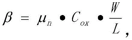
The EMI signal level changes from high to low causing transistor T5 to turn on. Accordingly, the driving transistor T1 is connected to the second power supply VDD, and I is connected as described belowOLEDConduction of current to the OLED:
CoxTo drive a transistorCapacitance of the gate oxide;
w is the width of the channel of the drive transistor;
l is the length of the channel of the drive transistor (i.e., the distance between the source and drain);
μnto drive the carrier mobility of the transistor.
Thus, the current to the OLED is independent of the threshold voltage of the drive transistor T1, and thus the current I to the OLED deviceOLEDWithout being affected by variations in the threshold voltage of the drive transistor. In this way, variations in the threshold voltage of the drive transistor have been compensated for.
Fig. 3 is a diagram depicting a second circuit configuration 20 according to an embodiment of the invention, and fig. 4 is a timing diagram associated with the circuit configuration of fig. 3. In this example, similar to the previous embodiment, the circuit 20 is configured as a TFT circuit including a plurality of transistors, in this embodiment, the transistors are p-type transistors (T1-T6), and Cst is a capacitor. The circuit element drives a light emitting device such as, for example, an OLED. The light emitting device (OLED) has an associated internal capacitance, which is denoted C in the circuit diagramoled. T1 is a driving transistor as an analog TFT, T2-T6 is a digital switching TFT, and T6 is an additional transistor in this embodiment. ColedIs the internal capacitance (i.e., C) of the OLED deviceoledNot a separate component but inherent to the OLED). The OLED is also connected to a first power source ELVSS.
Compared to the previous embodiment, a fixed VDAT _ INIT voltage signal is added and applied through an additional sixth transistor T6 connected to the third terminal of the driving transistor T1. The application of VDAT _ INIT is controlled by the adjacent (e.g., previous) row SCAN signal SCAN (n-1) for threshold voltage compensation (i.e., "n" represents the current row, thus, "n-1" represents the previous row, thus SCAN (n-1) is the same signal as the SCAN (n) signal of the previous row n). Input VDAT provides a data voltage for each row. In this way, programming speed or accuracy can be improved. Specifically, as shown with reference to the timing diagram of FIG. 4, the horizontal time is significantly reduced by performing threshold voltage compensation using the signal input SCAN (n-1) from the previous row. This enhanced efficiency is a trade-off with the use of the additional sixth transistor T6 resulting in a larger circuit compared to the previous embodiment.
The pixel circuit 20 of this embodiment may also operate in a first initialization phase during which memory effects from the residual voltage of a previous frame are substantially eliminated. During this first initialization phase, the EMI (n) signal level (EMI signal of the current row) is set to a high voltage level, causing transistor T5 to turn off. Accordingly, the source of the driving transistor T1 is disconnected from the power supply VDD. The initialization voltage INIT is also changed from a high reference voltage level similar to the low light emission voltage INIT _ H at the anode of the OLED to a low reference voltage level INIT _ L that can reverse-bias the OLED as described above without degrading the performance of the OLED, compared to the previous embodiments.
Further, during the first initialization phase, the SCAN1(n) signal level (SCAN 1 signal for the current row) changes from a high voltage level to a low voltage level, causing the transistor T3 to turn on. Therefore, a low initialization voltage INIT _ L is applied at the anode of the OLED. Any residual voltage and memory effects from the previous frame will reset to INIT _ L. The SCAN2(n) signal level also changes from high to low, causing transistor T2 to turn on. Accordingly, the driving transistor T1 is diode-connected through the transistor T2, so that the gate and drain of the driving transistor T1 are also initialized to INIT _ L through T2 and T3. In the case where the driving transistor T1 is diode-connected, an initialization voltage is also applied to the first (top) plate of the storage capacitor Cst. Similar to the previous embodiment, T3 preferably turns on before T2.
Furthermore, during the first initialization phase, the reference voltage VREF at the second (bottom) plate of the storage capacitor Cst is reduced to an intermediate reference level VREF _ M as part of the initialization. At the end of the initialization phase, the SCAN1(N) signal level changes from low to high, causing transistor T3 to turn off, which floats node N1.
Next, the TFT circuit 20 may operate in a threshold voltage compensation phase during which any variation in the threshold voltage of the driving transistor T1 is compensated for. During such phase, the SCAN (n-1) signal level (SCAN signal from the previous row) changes from a high voltage level to a low voltage level, causing transistor T6 to turn on. Thus, it is possible to provideThe fixed voltage VDAT _ INIT is applied to the source of the driving transistor. The diode connection node of the driving transistor is pulled up to V of the driving transistor T1GS(gate-source voltage) equal to threshold voltage VTH. At the end of this phase, the voltage at node N1 is VDAT _ INIT + VTH. The voltage VDAT _ INIT is set higher than the highest data voltage range but low enough to ensure that the OLED does not conduct during threshold voltage compensation.
Similar to the previous description, for effective threshold voltage compensation of the drive transistor T1, the applied VDAT voltage should be higher than VTH+VINIT_L+ΔV:
VDAT>|VTH|+VINIT_L+ΔV
Therefore, the following relationship is satisfied:
at the end of this phase, the SCAN (n-1) signal level changes from low to high, causing transistor T6 to turn off.
The TFT circuit 20 may then operate in a data programming phase during which the data voltages are programmed to drive the OLEDs during a subsequent light emitting phase. During the programming phase, the data voltage changes from the previous row data VDAT (n-1) to the current row data VDAT (n). Scan (n) the signal level changes from a high voltage level to a low voltage level, causing transistor T4 to turn on. The data voltage vdat (n) is applied to the source of the driving transistor. The reference voltage VREF at the second (bottom) plate of the capacitor is lowered to a level VREF _ L, which drives the gate voltage V of transistor T1N2Pulling to:
VINIT_L≤VN2<VDATlowest+VTH
thus, at the end of this phase, the voltage at node N1 is VDAT (N) + VTH. In addition, the scan (n) signal level changes from low to high, causing transistor T4 to turn off. The source of the driving transistor T1 becomes floating. The SCAN2(n) signal level changes from low to high, causing the transistor T2 to turn off and drive the gate of the transistor T1The drain is turned off so that the driving transistor T1 is no longer diode-connected through the transistor T2 and the current data voltage is effectively stored by the storage capacitor Cst.
Next, the TFT circuit 20 may operate in a light emission phase in which the OLED is capable of emitting light. At the beginning of this phase, a light emitting second initialization phase may be performed. During the second initialization phase of light emission, the voltage across the OLED is initialized or reset in preparation for the remaining light emission phase. This stage, like the previous embodiment, improves the threshold voltage compensation accuracy, especially for low light emission currents. During this light emission second initialization phase, the initialization voltage INIT changes from the first low voltage level INIT _ L to the second high voltage level INIT _ H. The SCAN1(n) signal level changes from a high voltage level to a low voltage level and transistor T3 turns on. The node N1 connecting the drain of the driving transistor T1 and the anode of the OLED is connected to INIT _ H.
As described above, the drain voltage of the driving transistor T1 may be different at the end of the threshold voltage compensation phase. If the programming current for emitting light is low, it may take a long time for the drain voltage of the driving transistor T1 to recover. The voltage at the anode of the OLED may vary, and thus light emission may vary according to the threshold voltage of the driving transistor T1. By reinitializing the node N1, the start voltage is the same level even if the threshold voltage changes.
At the end of the second initialization phase of light emission, the SCAN1(n) signal level changes from low to high, causing transistor T3 to turn off. In addition, VREF is also raised to a high voltage level VREF _ H, raising the gate voltage of the driver transistor T1 device to the desired operating voltage range:
VN2=VDAT+VTH+ΔVREF
referring again to the emission phase, the emi (n) signal level changes from the high voltage level to the low voltage level, causing transistor T5 to turn on. Accordingly, the driving transistor T1 is connected to the second power source VDD and conducts current to the OLED as follows:
CoxA capacitor which is a gate oxide of the driving transistor;
w is the width of the channel of the drive transistor;
l is the length of the channel of the drive transistor (i.e., the distance between the source and drain);
μnto drive the carrier mobility of the transistor.
Thus, the current to the OLED is independent of the threshold voltage of the drive transistor T1, and thus the current I to the OLED deviceOLEDWithout being affected by variations in the threshold voltage of the drive transistor. In this way, variations in the threshold voltage of the drive transistor have been compensated for.
Although the embodiments described herein are circuits using p-type TFTs, those skilled in the art can also apply the present invention to circuits using n-type TFTs. Further, although the embodiments described herein include a light emitting device having an anode connected to a driving transistor, a cathode of the light emitting device may be connected to the driving transistor instead. For example, for a circuit using an n-type TFT and a cathode of a light emitting device connected to a driving transistor, the advantages of the described circuit configuration can be obtained.
The described pixel circuit has advantages over conventional configurations. This circuit configuration enables compensation for threshold voltage variations with fewer transistors than conventional configurations, and additionally eliminates possible memory effects of the OLED device and drive transistor associated with a previous frame. The described circuit configuration thus improves the ability of the pixel to emit very little or no light, and therefore has a true black state, and is within a wide range of data values. The pixel circuit configuration of the present disclosure further improves true blackness by reverse biasing the OLED during the phase prior to light emission, and in particular, by further employing the light emission second initialization phase, the accuracy of threshold voltage compensation of the drive circuit is improved, especially for low OLED currents. In addition, the voltage range of the pixel circuit (i.e. the difference between the highest voltage in the pixel circuit and the lowest voltage in the pixel circuit) is reduced while still providing an efficient compensation of the threshold voltage of the drive transistor. The reduced range of the pixel circuit results in lower power consumption of the driver of the display compared to conventional configurations.
These advantages may be achieved using as few as five transistors and one storage capacitor, thereby providing a smaller circuit than conventional configurations. By adding the sixth transistor in the second embodiment, although the circuit size is increased, the circuit size is still small as compared with the conventional configuration, and a significantly shortened horizontal time is realized.
Various embodiments have been described in connection with OLEDs as display light emitting devices. However, the circuit configuration is not limited to any particular display technology. For example, the circuit configuration may also be used for micro LED displays, quantum dot LED displays, or any other device that emits light in response to an applied electrical bias. For example, a micro LED is a semiconductor device that includes a p-type region, an n-type region, and a light emitting region (e.g., formed on a substrate and separated into individual chips). Micro LEDs may be based on group III nitride semiconductors. Quantum dot LEDs are, for example, devices comprising a hole transport layer, an electron transport layer, and a light emitting region, wherein the light emitting region comprises nanocrystalline quantum dots. The circuit configurations described herein may be used for any such display technology.
One aspect of the present invention is a pixel circuit for a display device, which performs compensation of a variation in characteristics of a driving transistor in a small configuration, and additionally removes a possible memory effect from a previous frame. In an exemplary embodiment, the pixel circuit includes a driving transistor configured to control an amount of current to the light emitting device according to a voltage applied to a gate of the driving transistor; a second transistor connected to the gate of the driving transistor and the second terminal of the driving transistor such that when the second transistor is in an on state, the driving transistor becomes diode-connected such that the gate and the second terminal of the driving transistor are connected through the second transistor; a light emitting device connected to the second terminal of the driving transistor at a first node and connected to the first voltage source at a second node; a third transistor connected between the initialization voltage source and a first node of the light emitting device, wherein a node N1 is a connection point of the second terminal of the driving transistor, the first node of the light emitting device, and the third transistor; and at least one capacitor having a first plate connected to the gate of the driving transistor and a second plate connectable to a reference voltage source. The pixel circuit may include one or more of the following features, either alone or in combination.
In an exemplary embodiment of the pixel circuit, the pixel circuit may be operated in an initialization stage, and during the initialization stage, the second and third transistors are in a turned-on state such that the first initialization voltage is connected to the first plate of the capacitor, the gate of the driving transistor, and the first node of the light emitting device.
In an exemplary embodiment of the pixel circuit, the first initialization voltage is lower than the first voltage source.
In an exemplary embodiment of the pixel circuit, the pixel circuit is operable in a compensation phase, and during the compensation phase, the reference data voltage is applied at the third terminal of the drive transistor, and the reference voltage applied at the second plate of the capacitor has a first voltage; and the pixel circuit may be operated in a programming phase, and during the programming phase, a data voltage corresponding to a gray scale value is applied at the third terminal of the driving transistor, and a reference data voltage applied to the second plate of the capacitor has a second voltage.
In an exemplary embodiment of the pixel circuit, the pixel circuit may further be operated during a light emitting second initialization phase in which the third transistor is in an on state to connect the second initialization voltage to the node N1.
In an exemplary embodiment of the pixel circuit, the pixel circuit further includes a fourth transistor connected to the third terminal of the driving transistor.
In an exemplary embodiment of the pixel circuit, the pixel circuit further comprises a fifth transistor connected to the third terminal of the drive transistor, wherein during the light emission phase the fifth transistor is in a conducting state to connect the drive transistor to the second transistor voltage source and the reference voltage has the third voltage.
In an exemplary embodiment of the pixel circuit, the pixel circuit further comprises a sixth transistor connected to the third terminal of the drive transistor, wherein during the compensation phase the sixth transistor is in a conducting state to apply the fixed voltage to the third terminal of the drive transistor.
In an exemplary embodiment of the pixel circuit, all the transistors are p-type transistors.
In an exemplary embodiment of the pixel circuit, the first node of the light emitting device is an anode and the second node of the light emitting device is a cathode.
In an exemplary embodiment of the pixel circuit, the light emitting device is one of an organic light emitting diode, a micro Light Emitting Diode (LED), or a quantum dot LED.
Another aspect of the present invention is a method of operating a pixel circuit for a display device, comprising the steps of: providing a pixel circuit according to any embodiment; and performs an initialization phase, a compensation phase, a programming phase, and a light emitting phase. During the initialization phase, memory effects from previous frames are reduced by performing the following steps: placing the fourth transistor in an off state and placing the fifth transistor in an off state to disconnect the second voltage source from the pixel circuit; placing the third transistor in an on state to apply a first initialization voltage to a first node of the light emitting device; setting a reference voltage to a first voltage; placing the second transistor in a conducting state, wherein the driving transistor becomes diode-connected through the second transistor such that the first initialization voltage is applied to the gate of the driving transistor and the first plate of the capacitor; and placing the third transistor in an off state at the end of the initialization phase. During the compensation phase, the threshold voltage of the drive transistor is compensated at least in part by: placing the fourth transistor in a conducting state and applying a reference data voltage to the third terminal of the driving transistor through the fourth transistor, wherein the reference data voltage is set such that a voltage across the light emitting device is lower than a threshold voltage of the light emitting device. During the programming phase, the data voltage corresponding to the current gray value is applied by: setting the reference voltage to a second voltage for programming the entire data range; and changing the data voltage source from the reference data voltage to a present data voltage corresponding to a required current through the light emitting device during the light emitting phase; placing the fourth transistor in an off state after the current data voltage is applied; and placing the second transistor in a blocking state such that the drive transistor is no longer diode connected, wherein the present data voltage is stored by the storage capacitor. The lighting phase comprises the following steps: setting the reference voltage to a third voltage to change a gate voltage of the driving transistor to an operating voltage range, wherein the driving transistor controls an amount of current to the light emitting device; placing the fifth transistor in a conducting state to connect the second power source to the driving transistor; and controls the amount of current to the light emitting device according to the voltage at the gate of the driving transistor. The method of operation may include one or more of the following features, either alone or in combination.
In an exemplary embodiment of the method of operating, the third transistor is placed in a conducting state before the second transistor is placed in a conducting state during the initialization phase.
In an exemplary embodiment of the method of operating, the first initialization voltage reverse biases the light emitting device.
In an exemplary embodiment of the operating method, the reference voltage applied to the second plate of the storage capacitor is a multi-level voltage that is different during the first initialization phase and the programming phase.
In an exemplary embodiment of the operation method, the reference data voltage is a data value corresponding to a lowest gray scale value of the light emitting device.
In an exemplary embodiment of the method of operation, the method of operation further comprises: after the programming phase and at the beginning of the light emitting phase, performing a light emitting second initialization phase to reset the voltage at the first node of the light emitting device by: placing the third transistor in an on state and applying a second initialization voltage to the first node of the light emitting device; and changes the state of the third transistor from an on state to an off state.
In an exemplary embodiment of the method of operation, the first initialization voltage is a lower voltage than the second initialization voltage,
in an exemplary embodiment of the operation method, the pixel circuit further includes a sixth transistor connected to the third terminal of the driving transistor, wherein during the compensation phase, the sixth transistor is in a conductive state to apply the fixed voltage to the third terminal of the driving transistor through the sixth transistor.
In an exemplary embodiment of the method of operating, the light emitting device is one of an organic light emitting diode, a micro Light Emitting Diode (LED), or a quantum dot LED.
Although the invention has been shown and described with respect to a certain embodiment or embodiments, it is obvious that equivalent alterations and modifications will occur to others skilled in the art upon the reading and understanding of this specification and the annexed drawings. In particular regard to the various functions performed by the above described elements (components, assemblies, devices, compositions, etc.), the terms (including a reference to a "means") used to describe such elements are intended to correspond, unless otherwise indicated, to any element which performs the specified function of the described element (i.e., that is functionally equivalent), even though not structurally equivalent to the disclosed structure which performs the function in the herein illustrated exemplary embodiment or embodiments of the invention. In addition, while a particular feature of the invention may have been described above with respect to only one or more of several illustrated embodiments, such feature may be combined with one or more other features of the other embodiments, as may be desired and advantageous for any given or particular application.
Industrial applicability
Embodiments of the present invention are applicable to many display devices to allow for high resolution display devices with effective threshold voltage compensation and true black performance. Examples of such devices include televisions, mobile phones, Personal Digital Assistants (PDAs), tablet and laptop computers, desktop monitors, digital cameras, and similar devices where high resolution displays are desired.