This application is related to the following U.S. non-provisional applications, each of which is incorporated herein by reference in its entirety.
Each of the above non-provisional applications claims priority based on the following U.S. provisional applications, each of which is incorporated herein by reference in its entirety.
This application is also related to the following concurrently filed U.S. non-provisional applications, each of which is incorporated herein by reference in its entirety.
Detailed Description
Processor with architected neural network elements
Referring now to FIG. 1, a block diagram illustrating a processor 100 including a Neural Network Unit (NNU)121 is shown. Processor 100 includes instruction fetch unit 101, instruction cache 102, instruction translator 104, rename unit 106, reservation stations 108, media registers 118, General Purpose Registers (GPRs) 116, execution units 112 other than NNUs 121, and memory subsystem 114.
Processor 100 is an electronic device that functions as a Central Processing Unit (CPU) on an integrated circuit. Processor 100 receives digital data as input, processes the data according to instructions fetched from memory, and generates as output the results of operations specified by the instructions. The processor 100 may be used in a desktop, mobile, or tablet computer, and for purposes such as computing, text editing, multimedia display, and internet browsing. The processor 100 may also be provided in an embedded system to control a wide variety of devices including home appliances, mobile phones, smart phones, automobiles, and industrial control devices. A CPU is an electronic circuit (i.e., "hardware") that executes instructions of a computer program (also referred to as a "computer application" or "application") by performing operations including arithmetic operations, logical circuit operations, and input/output operations on data. Integrated Circuits (ICs) are a group of electronic circuits fabricated on a small piece of semiconductor material, typically silicon. An IC is also known as a chip, microchip, or die.
Instruction fetch unit 101 controls the fetching of architectural instructions 103 into instruction cache 102 from system memory (not shown). Instruction fetch unit 101 provides a fetch address to instruction cache 102 that specifies a memory address in instruction cache 102 to which processor 100 fetches a cache line of architectural instruction bytes. The fetch address is based on the current value of the program counter or an instruction pointer (not shown) of the processor 100. Typically, the program counter is incremented in order of the size of the instruction unless a control instruction, such as a branch, call, or return instruction, is encountered in the instruction stream, or an exception condition, such as an interrupt, trap, exception, or fault occurs, in which case the program counter is updated with a non-sequential address, such as a branch target address, return address, or exception vector. Generally, the program counter is updated in response to execution of an instruction by execution unit 112/121. The program counter may also be updated in response to detecting an exception condition, such as instruction converter 104 encountering an instruction 103 not defined by the instruction set architecture of processor 100.
Instruction cache 102 caches architectural instructions 103 fetched from system memory coupled to
processor 100. The architecture instructions 103 include Move To Neural Network (MTNN) instructions and Move From Neural Network (MFNN) instructions, which will be described in more detail below. In one embodiment, the architectural instructions 103 are x86 Instruction Set Architecture (ISA) instructions, with the addition of MTNN and MFNN instructions. In the context of the present disclosure, an x86 ISA processor is generated and operated at the instruction set architecture level
Processing of identical results generated when processors execute identical machine language instructionsA device. However, other embodiments contemplate other instruction set architectures, such as advanced RISC machines
Sun
Or
The instruction cache 102 provides the architectural instructions 103 to the
instruction converter 104, and the
instruction converter 104 converts the architectural instructions 103 into the
microinstructions 105.
The microinstructions 105 are provided to the rename unit 106 and are ultimately executed by the execution unit 112/121. The microinstructions 105 implement architectural instructions. Preferably, the instruction converter 104 includes a first portion that converts frequently executed and/or relatively less complex architectural instructions 103 into microinstructions 105. The instruction converter 104 also includes a second portion that includes a microcode unit (not shown). The microcode unit includes a microcode memory that holds microcode instructions that implement complex and/or infrequently used instructions of the architectural instruction set. The microcode unit also includes a micro-sequencer that provides a non-architected micro-program counter (micro-PC) to the microcode memory. Preferably, the microcode instructions are converted to microinstructions 105 by a micro-converter (not shown). The selector selects microinstructions 105 from either the first portion or the second portion for providing to the rename unit 106 depending on whether the microcode unit currently has control.
Rename unit 106 renames architectural registers specified in architectural instruction 103 to physical registers of processor 100. Preferably, processor 100 includes a reorder buffer (not shown). The rename unit 106 allocates an entry in a reorder buffer for each microinstruction 105 in program order. This enables the processor 100 to retire the microinstructions 105 and their corresponding structure instructions 103 in program order. In one embodiment, media registers 118 are 256 bits wide and GPRs 116 are 64 bits wide. In one embodiment, the media register 118 is an x86 media register, such as an advanced vector extensions (AVX) register.
In one embodiment, each entry in the reorder buffer includes storage for the results of microinstructions 105; in addition, processor 100 includes an architectural register file that includes a physical register for each architectural register (e.g., media registers 118 and GPRs 116, as well as other architectural registers). (e.g., there are preferably separate register files for media registers 118 and GPRs 116 because they are different in size.) for each source operand of a microinstruction 105 that specifies an architectural register, the rename unit populates the source operand field in the microinstruction 105 with the reorder buffer index of the newest old microinstruction 105 written to the architectural register. When the execution unit 112/121 completes execution of the microinstruction 105, it writes the result to the reorder buffer entry of the microinstruction 105. When micro instruction 105 retires, a retirement unit (not shown) writes the results from the micro instruction's reorder buffer entry to a register of the physical register file associated with the architectural destination register specified by retirement micro instruction 105.
In another embodiment, processor 100 includes a physical register file that includes more physical registers than the number of architectural registers, but does not include an architectural register file, and the reorder buffer entry does not include a result store. (e.g., there are preferably separate physical register files for media registers 118 and GPRs 116 because they are different sizes.) processor 100 also includes a pointer table with an associated pointer for each architectural register. For operands of the microinstruction 105 that specify architectural registers, the rename unit populates the destination operand field in the microinstruction 105 with pointers to free registers in the physical register file. Rename unit 106 stalls the pipeline if no registers in the physical register file are free. For each source operand of a microinstruction 105 that specifies an architectural register, the rename unit populates the source operand field in the microinstruction 105 with a pointer to a register in the physical register file assigned to the newest old microinstruction 105 that writes to the architectural register. When the execution unit 112/121 completes execution of the microinstruction 105, it writes the result to the register of the physical register file pointed to by the destination operand field of the microinstruction 105. When the microinstruction 105 retires, the retirement unit copies the destination operand field value of the microinstruction 105 to a pointer in the pointer table associated with the architectural destination register specified by the retirement microinstruction 105.
The reservation station 108 holds the microinstructions 105 until they are ready to be issued to the execution unit 112/121 for execution. The microinstruction 105 is ready to be issued when all of its source operands are available and the execution unit 112/121 is available to execute the microinstruction 105. Execution unit 112/121 receives register source operands from a reorder buffer or architectural register file as described above in the first embodiment or from a physical register file as described above in the second embodiment. Additionally, execution unit 112/121 may receive register source operands directly from execution unit 112/121 via a result forwarding bus (not shown). Additionally, the execution unit 112/121 may receive an immediate operand specified by the microinstruction 105 from the reservation station 108. As discussed in more detail below, the MTNN and MFNN architecture instruction 103 includes an immediate operand that specifies a function to be executed by the NNU 121 that is provided in one of the one or more microinstructions 105 into which the MTNN and MFNN architecture instruction 103 is translated.
Execution units 112 include one or more load/store units (not shown) that load data from memory subsystem 114 and store data to memory subsystem 114. Preferably, memory subsystem 114 includes a memory management unit (not shown) that may include, for example, a translation lookaside buffer and table line (tablewalk) unit, a level one data cache (and instruction cache 102), a level two unified cache, and a bus interface unit that interfaces processor 100 to system memory. In one embodiment, processor 100 of FIG. 1 represents a processing core that is one of multiple processing cores in a multi-core processor that shares a last level cache memory. Execution units 112 may also include integer units, media units, floating point units, and branch units.
NNU 121 includes a weighted Random Access Memory (RAM)124, a data RAM 122, N Neural Processing Units (NPUs) 126, a program memory 129, a sequencer 128, and control and status registers 127. The NPU 126 conceptually functions as a neuron in a neural network. The weight RAM 124, data RAM 122 and program memory 129 are writable and readable by means of the MTNN and MFNN architecture instructions 103, respectively. The weight RAM 124 is arranged as W rows of N weight words and the data RAM 122 is arranged as D rows of N data words. Each data word and each weight word is a plurality of bits, preferably 8, 9, 12 or 16 bits. Each data word serves as an output value (sometimes also referred to as an activation) for a neuron of a previous layer in the network, and each weight word serves as a weight associated with a connection into a neuron of a current layer of the network. While in many uses of NNU 121, the words or operands stored in weight RAM 124 are actually weights associated with connections into neurons, it should be understood that in other uses of NNU 121, the words stored in weight RAM 124 are not weights, but are also referred to as "weight words" because they are stored in weight RAM 124. For example, in some uses of NNU 121, such as the convolution examples of fig. 24-26A or the pooling examples of fig. 27-28, weight RAM 124 may hold non-weights, such as elements of a data matrix, e.g., image pixel data. Similarly, while in many uses of NNU 121, the words or operands stored in data RAM 122 are actually output values or activations of neurons, it should be understood that in other uses of NNU 121, the data stored in data RAM 122 is not, but is also referred to as "data words" because they are stored in data RAM 122. For example, in some uses of NNU 121, such as the convolution examples of fig. 24-26A, data RAM 122 may hold non-neuronal outputs, such as elements of a convolution kernel.
In one embodiment, the NPU 126 and the sequencer 128 comprise combinational logic, sequential logic, state machines, or a combination thereof. An architectural instruction (e.g., MFNN instruction 1500) loads the contents of status register 127 into one of GPRs 116 to determine the status of NNU 121, e.g., NNU 121 has completed a command or completed a program from program memory 129 that NNU 121 runs, or NNU 121 may be free to receive a new command or begin a new NNU program.
Advantageously, the number of NPUs 126 may be increased as desired, the weight RThe size of the AM 124 and data RAM122 may be expanded in both width and depth accordingly. Preferably, the weight RAM 124 is large because there are many connections associated with each neuron in a typical neural network layer, and thus there are multiple weights. Various embodiments are described herein regarding the size of the data words and weight words, as well as the size of the weight RAM 124 and data RAM122, and the number of NPUs 126. In one embodiment, the NNU 121 with 64KB (8192 bits by 64 rows) data RAM122, 2MB (8192 bits by 2048 rows) weight RAM 124, and 512 NPUs 126 is implemented in Taiwan semiconductor manufacturing Limited (TSMC)16nm technology, and occupies approximately 3.3mm 2The area of (a).
Sequencer 128 fetches instructions from program memory 129 and executes them, including generating address and control signals for supply to data RAM 122, weight RAM 124, and NPU 126. The sequencer 128 generates a memory address 123 and a read command for supply to the data RAM 122 to select one of the D rows of N data words for supply to the N NPUs 126. Sequencer 128 also generates memory addresses 125 and read commands for providing to weight RAM 124 to select one of the W rows of N weight words for providing to the N NPUs 126. The sequence of addresses 123 and 125 provided to the NPU126, generated by the sequencer 128, determines the "connections" between the neurons. The sequencer 128 also generates memory addresses 123 and write commands for providing to the data RAM 122 to select one of the D rows of N data words to write from the N NPUs 126. Sequencer 128 also generates memory addresses 125 and write commands for providing to weight RAM 124 to select one of the W rows of N weight words to write from the N NPUs 126. Sequencer 128 also generates a memory address 131 to program memory 129 to select the NNU instruction provided to sequencer 128, as described below. The memory address 131 corresponds to a program counter (not shown) that the sequencer 128 typically increments through sequential locations of the program memory 129 unless the sequencer 128 encounters a control instruction, such as a loop instruction (see, e.g., FIG. 26A), in which case the sequencer 128 updates the program counter to the target address of the control instruction. The sequencer 128 also generates control signals to the NPUs 126 to instruct them to perform various operations or functions, such as initialization, arithmetic/logical operations, rotate and shift operations, activate functions, and write back operations, examples of which are described in more detail below (see, e.g., micro-operation 3418 of fig. 34).
The N NPUs 126 generate N result words 133, which may be written back to a row of weight RAM124 or data RAM 122. Preferably, the weight RAM124 and the data RAM 122 are directly coupled to the N NPUs 126. More specifically, the weight RAM124 and the data RAM 122 are dedicated to the NPU126 and are not shared by other execution units 112 of the processor 100, and the NPU126 is able to use up rows from one or both of the weight RAM124 and the data RAM 122 in a persistent manner (preferably in a pipelined manner) each clock cycle. In one embodiment, each of data RAM 122 and weight RAM124 can provide 8192 bits to NPU126 at each clock cycle. 8192 bits may be used as 512 16-bit words or 1024 8-bit words, as described in more detail below.
Advantageously, the size of the data sets that may be processed by the NNU 121 is not limited to the size of the weight RAM124 and the data RAM 122, but is only limited by the size of the system memory, as the data and weights may be moved between the system memory and the weight RAM124 and the data RAM 122 using the MTNN and MFNN instructions (e.g., via the media registers 118). In one embodiment, the data RAM 122 is dual ported to enable data words to be written to the data RAM 122 while the data words are simultaneously read from or written to the data RAM 122. In addition, the large memory hierarchy of memory subsystem 114, including cache memory, provides very high data bandwidth for transfers between system memory and NNU 121. Further, memory subsystem 114 preferably includes a hardware data prefetcher that tracks memory access patterns (such as neural data and weight loads from system memory), and performs data prefetching into the cache hierarchy to facilitate high bandwidth and low latency transfers to weight RAM124 and data RAM 122.
Although embodiments are described in which one of the operands provided to each NPU 126 is provided from a weight store and represented as weights commonly used in neural networks, it should be understood that the operands may be other types of data associated with calculations whose speed may be improved by the described apparatus.
Referring now to fig. 2, a block diagram illustrating the NPU 126 of fig. 1 is shown. The NPU 126 operates to perform a number of functions or operations. In particular, the NPU 126 is advantageously configured to operate as a neuron or node in an artificial neural network to perform typical multiply-accumulate functions or operations. That is, in general, the NPU 126 (neuron) is configured to: (1) receiving an input value from each neuron connected to it, typically but not necessarily from a previous layer of the artificial neural network; (2) multiplying each input value by a corresponding weight value associated with the connection to generate a product; (3) adding all products to generate a sum; and (4) performing an activation function on the sum to generate an output of the neuron. However, rather than performing all multiplications associated with all connected inputs and then adding all products together as is conventional, each neuron is advantageously configured to perform a weighted multiplication operation associated with one of the connected inputs in a given clock cycle and then add (accumulate) that product with the accumulated value of the product associated with the connected input processed in the preceding clock cycle up to that point. Assuming there are M connections to the neuron, after all M products have been accumulated (which takes about M clock cycles), the neuron performs an activation function on the accumulated value to generate an output or result. This has the advantage of requiring fewer multipliers and smaller, simpler and faster adder circuits (e.g., 2-input adders) in the neuron, as compared to adders that need to add all or even a subset of the products associated with all connected inputs. This, in turn, has the advantage of favoring a very large number (N) of neurons in NNU121 (NPU 126), such that after about M clock cycles, NNU121 has generated outputs for all of the large number (N) of neurons. Finally, NNUs 121, which are made up of such neurons, have the advantage of performing effectively as an artificial neural network layer for a large number of different connection inputs. That is, as M increases or decreases for different layers, the number of clock cycles required to generate the neuron output increases or decreases accordingly, leveraging resources (e.g., multipliers and accumulators); while in more conventional designs some multipliers and a portion of the adders may not be used for smaller values of M. Thus, the embodiments described herein have the benefit of flexible and efficient number of connection inputs to the neurons of NNUs 121, and provide extremely high performance.
The NPU 126 includes a register 205, a 2-input multiplexing register (mux-reg)208, an Arithmetic Logic Unit (ALU)204, an accumulator 202, and an Activation Function Unit (AFU) 212. Register 205 receives weight word 206 from weight RAM 124 and provides its output 203 on a subsequent clock cycle. The multiplexer register 208 selects one of its inputs 207 or 211 for storage in its register and then is provided on its output 209 on a subsequent clock cycle. An input 207 receives the data word from the data RAM 122. Another input 211 receives the output 209 of the adjacent NPU 126. The NPU 126 shown in fig. 2 is represented as NPU J from the N NPUs 126 of fig. 1. That is, NPU J is a representative example of N NPUs 126. Preferably, the multiplexing register 208 input 211 of NPU J receives the multiplexing register 208 output 209 of NPU 126 instance J-1, and the multiplexing register 208 output 209 of NPU J is provided to the multiplexing register 208 input 211 of NPU 126 instance J + 1. In this manner, the multiplexing registers 208 of the N NPUs 126 collectively operate as an N-word rotator or cyclic shifter, as described in more detail below with respect to fig. 3. The control input 213 controls the multiplexer register 208 to select which of the two inputs is stored in its register and subsequently provided on the output 209.
The ALU 204 has three inputs. One input receives a weight word 203 from a register 205. The other input receives the output 209 of the multiplexer register 208. Yet another input receives the output 217 of the accumulator 202. The ALU 204 performs arithmetic and/or logical operations on its inputs to generate results provided on its outputs. Preferably, the arithmetic and/or logical operations performed by ALU 204 are specified by instructions stored in program memory 129. For example, the multiply-accumulate instruction of FIG. 4 specifies a multiply-accumulate operation, i.e., the result 215 is the sum of the value 217 of the accumulator 202 plus the product of the weight word 203 and the data word at the output 209 of the multiplex register 208. Other operations that may be specified include, but are not limited to: result 215 is the pass value of the mux register output 209; result 215 is the pass value of weight word 203; result 215 is zero; result 215 is the pass value of weight word 203; the result 215 is the sum of the value 217 of the accumulator 202 and the weight word 203; result 215 is the sum of the value 217 of accumulator 202 and the multiplexed register output 209; result 215 is the value 217 of accumulator 202 and the maximum value of weight word 203; result 215 is the value 217 of accumulator 202 and the maximum value of the multiplexed register output 209.
The ALU 204 provides its output 215 to the accumulator 202 for storage therein. The ALU 204 includes a multiplier 242, and the multiplier 242 multiplies the weight word 203 with the data word at the output 209 of the multiplexing register 208 to generate a product 246. In one embodiment, multiplier 242 multiplies two 16-bit operands to generate a 32-bit result. The ALU 204 also includes an adder 244 that adds a product 246 to the accumulator 202 output 217 to generate a sum, which is the result 215 accumulated in the accumulator 202 for storage in the accumulator 202. In one embodiment, adder 244 adds the 32-bit result of multiplier 242 to the 41-bit value 217 of accumulator 202 to generate a 41-bit result. In this way, using the rotator scheme of the multiplexing register 208 over the course of multiple clock cycles, the NPU 126 completes the summation of the product of the neurons required by the neural network. The ALU 204 may also include other circuit elements to perform other arithmetic/logic operations such as those described above. In one embodiment, a second adder subtracts the weight word 203 from the data word at output 209 of the multiplexing register 208 to generate a difference, and adder 244 then adds this difference to output 217 of accumulator 202 to generate sum 215, and sum 215 is the result of accumulation in accumulator 202. In this way, the NPU 126 may complete the sum of the differences over the course of multiple clock cycles. Preferably, although the weight word 203 and the data word 209 have the same size (in bits), they may have different binary point locations, as described in more detail below. Preferably, the multipliers 242 and adders 244 are integer multipliers and adders, as described in more detail below, to advantageously implement a simpler, smaller, faster, and lower power ALU 204 than the floating point peer-to-peer scheme. However, it should be understood that in other embodiments, ALU 204 performs floating point operations.
Although FIG. 2 only shows the multiplier 242 and adder 244 in the ALU204, preferably the ALU204 includes other elements for performing the other operations described above. For example, the ALU204 preferably includes a comparator (not shown) for comparing the accumulator 202 with the data/weight words and a multiplexer (not shown) that selects the larger (largest) of the two values indicated by the comparator for storage in the accumulator 202. For another example, the ALU204 preferably includes selection logic (not shown) that bypasses the multiplier 242 with a data/weight word to enable the adder 244 to add the data/weight word to the value 217 of the accumulator 202 to generate a sum for storage in the accumulator 202. These additional operations are described in more detail below, e.g., with respect to fig. 18-29A, and may be used, for example, to perform convolution and pooling operations.
AFU 212 receives output 217 of accumulator 202. AFU 212 performs an activation function on accumulator 202 output 217 to generate result 133 of fig. 1. In general, activation functions in neurons of intermediate layers of an artificial neural network can be used to optimally normalize the accumulated product sums in a non-linear manner. To "normalize" the accumulated sum, the activation function of the current neuron produces a result value that is within a range of values that the neuron connected to the current neuron expects to receive as input. (the normalized result is sometimes referred to as "active", and as described herein is the output of the current node multiplied by the receiving node by a weight associated with the connection between the output node and the receiving node to generate a product that is accumulated with other products associated with other input connections to the receiving node). For example, a receiving/connected neuron may expect to receive as input a value between 0 and 1, in which case the output neuron may need to nonlinearly squeeze and/or adjust (e.g., move up to convert negative values to positive values) the accumulated sum outside the 0 to 1 range to a value within the expected range. Thus, AFU 212 performs an operation on the value 217 of accumulator 202 to bring result 133 within a known range. The results 133 of all N NPUs 126 may be written back to the data RAM 122 or the weight RAM 124 simultaneously. Preferably, AFU 212 is configured To execute a plurality of activation functions, and for example, an input from the controller register 127 selects one of the activation functions to execute on the output 217 of the accumulator 202. Activation functions may include, but are not limited to, a step function, a correction function, a sigmoid function, a hyperbolic tangent (tanh) function, and a softplus function (also referred to as a smoothing correction). The softplus function is an analytical function f (x) ═ ln (1+ e)x) I.e. one and exWhere "e" is the euler number and x is the input 217 to the function. Preferably, the activation function may also include a pass function that passes the value 217 of the accumulator 202, or a portion thereof, as described in more detail below. In one embodiment, the circuitry of AFU 212 executes the activation function in a single clock cycle. In one embodiment, AFU 212 includes a table that receives accumulated values and outputs values that approximate the values that a true activation function would provide for some activation functions (e.g., sigmoid, hyperbolic tangent, softplus).
Preferably, the width (in bits) of accumulator 202 is greater than the width of AFU 212 output 133. For example, in one embodiment, the accumulator is 41 bits wide to avoid loss of precision in the accumulation of up to 512 32-bit products (as described in more detail below, e.g., with respect to FIG. 30), and the result 133 is 16 bits wide. In one embodiment, an example of which is described in more detail below with respect to FIG. 8, during successive clock cycles different portions of the value of the "raw" accumulator 202 output 217 pass through AFU 212 and are written back to data RAM 122 or weight RAM 124. This enables the raw accumulator 202 values to be loaded back to the media registers 118 via the MFNN instruction, such that instructions executing on other execution units 112 of the processor 100 may execute complex activation functions that the AFU 212 is not capable of executing, such as the well-known softmax activation function, also known as a normalized exponential function. In one embodiment, processor 100 instruction set architecture includes execution of what is commonly referred to as e xOr the exponential function of exp (x), which may be used to accelerate the execution of the softmax activation function by other execution units 112 of the processor 100.
In one embodiment, the NPU 126 is pipelined. For example, the NPU 126 may include registers of the ALU 204, such as registers between multipliers and adders and/or other circuitry of the ALU 204, and registers to hold outputs of the AFU 212. Other embodiments of the NPU 126 are described below.
Referring now to FIG. 3, a block diagram illustrating an embodiment of an arrangement of N multiplex registers 208 of the N NPUs 126 of NNU 121 of FIG. 1 is shown to illustrate their operation as an N-word rotator or circular shifter for a row of data words 207 received from data RAM122 of FIG. 1. In the embodiment of FIG. 3, N is 512, so that NNU 121 has 512 multiplex registers 208, denoted 0 through 511, corresponding to 512 NPUs 126, as shown. Each multiplexing register 208 receives its corresponding data word 207 for one of the D rows of the data RAM 122. That is, mux register 0 receives data word 0 for the row of data RAM122, mux register 1 receives data word 1 for the row of data RAM122, mux register 2 receives data word 2 for the row of data RAM122, and so on until mux register 511 receives data word 511 for the row of data RAM 122. In addition, multiplexer register 1 receives on its further input 211 the output 209 of multiplexer register 0, multiplexer register 2 receives on its further input 211 the output 209 of multiplexer register 1, multiplexer register 3 receives on its further input 211 the output 209 of multiplexer register 2, and so on, up to multiplexer register 511, which receives on its further input 211 the output 209 of multiplexer register 510, and multiplexer register 0 receives on its further input 211 the output 209 of multiplexer register 511. Each of the multiplex registers 208 receives a control input 213 which controls whether the data word 207 or the rotation input 211 is selected. As described in more detail below, in one mode of operation, on a first clock cycle, the control input 213 controls each of the multiplexer registers 208 to select a data word 207 for storage in the register and subsequent supply to the ALU 204; during a subsequent clock cycle (e.g., M-1 clock cycles as described above), the control input 213 controls each of the multiplexer registers 208 to select the rotated input 211 for storage in the register and subsequent provision to the ALU 204.
Although fig. 3 (and fig. 7 and 19 below) illustrate an embodiment in which the NPU 126 is configured to rotate the value of the mux register 208/705 to the right, i.e., from NPU J to NPU J +1, embodiments are contemplated (such as the embodiments with respect to fig. 24-26) in which the NPU 126 is configured to rotate the value of the mux register 208/705 to the left, i.e., from NPU J to NPU J-1. Further, embodiments are contemplated in which the NPU 126 is configured to selectively rotate the value of the mux register 208/705 to the left or right, e.g., as specified by the NNU instruction.
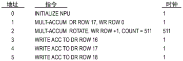
Referring now to FIG. 4, a table is shown that illustrates a program for storage in program memory 129 of NNU 121 of FIG. 1 and execution by NNU 121. An exemplary program performs the computations associated with the layers of the artificial neural network described above. In the table of fig. 4, four rows and three columns are shown. Each row corresponds to an address of the program memory 129 indicated in the first column. The second column specifies the instruction and the third column indicates the number of clock cycles associated with the instruction. Preferably, the number of clock cycles indicates the effective number of clocks per instruction clock type value in a pipelined embodiment, rather than the latency of the instruction. As shown, due to the pipelined nature of NNU 121, each instruction has an associated one clock cycle, except for the instruction at address 2, which requires 511 clocks, because it effectively repeats itself 511 times, as explained in more detail below.
For each instruction of the program, all NPUs 126 execute the instruction in parallel. That is, all N NPUs 126 execute instructions in the first row in the same clock cycle, all N NPUs 126 execute instructions in the second row in the same clock cycle, and so on. However, other embodiments are described below in which some instructions are executed in a partially parallel and partially sequential manner, such as the activate function and output instructions at addresses 3 and 4 in embodiments where the NPUs 126 share an activate function unit (e.g., as with the embodiment of fig. 11). The example of fig. 4 assumes one layer of 512 neurons (NPUs 126), each with 512 connection inputs from the previous layer of 512 neurons, for a total of 256K connections. Each neuron receives a 16-bit data value from each of the connected inputs and multiplies the 16-bit data value by an appropriate 16-bit weight value.
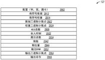
At address 0 (although other addresses may be specified), the first row specifies the initialize NPU instruction. The initialization instruction clears the value of the accumulator 202. In one embodiment, the initialization instruction may also specify loading the accumulator 202 with the corresponding word of the row of the data RAM 122 or weight RAM 124 whose address is specified by the instruction. The initialization instructions also load configuration values into control registers 127, as described in more detail below with respect to fig. 29A and 29B. For example, the width of the data word 207 and weight word 209 may be loaded, which may be used by the ALU 204 to determine the size of the operation performed by the circuit and may affect the result 215 stored in the accumulator 202. In one embodiment, the NPU 126 includes circuitry to saturate the ALU 204 output 215 prior to storage in the accumulator 202, into which an initialization instruction loads a configuration value to affect saturation. In one embodiment, the accumulator 202 may also be cleared to a zero value by so specifying in an ALU function instruction (e.g., a multiply-accumulate instruction at address 1) or an output instruction (e.g., a write AFU output instruction at address 4).
At address 1, the second row specifies a multiply-accumulate instruction that instructs 512 NPUs 126 to load a corresponding data word from one row of data RAM122 and a corresponding weight word from one row of weight RAM124, perform a first multiply-accumulate operation on data word input 207 and weight word input 206, which accumulates with initialized accumulator 202 with a zero value. More specifically, the instruction instructs the sequencer 128 to generate a value on the control input 213 to select the data word input 207. In the example of FIG. 4, the designated data RAM122 row is row 17 and the designated weight RAM124 row is row 0, which instructs sequencer 128 to output a value of 17 for data RAM address 123 and a value of 0 for weight RAM address 125. Thus, 512 data words from row 17 of the data RAM122 are provided to respective data inputs 207 of the 512 NPUs 126, and 512 weight words from row 0 of the weight RAM124 are provided to respective weight inputs 206 of the 512 NPUs 126.
At address 2, the third row specifies a multiply-accumulate rotate instruction with a count of 511 that instructs each of the 512 NPUs 126 to perform 511 multiply-accumulate operations. The instruction indicates 512 NPUs 126, and for each of 511 multiply-accumulate operations, the data word 209 input to the ALU 204 is the rotated value 211 from the adjacent NPU 126. That is, the instruction instructs the sequencer 128 to generate a value on the control input 213 that selects the rotation value 211. In addition, the instruction instructs 512 NPUs 126 to load a respective weight word for each of the 511 multiply-accumulate operations from the "next" row of weight RAM 124. That is, the instruction instructs the sequencer 128 to increment the weight RAM address 125 by 1 relative to its value in the previous clock cycle, which in this example would be row 1 on the first clock cycle, row 2 on the next clock cycle, row 3 on the next clock cycle, and so on, up to row 511 on the 511 th clock cycle. For each of the 511 multiply-accumulate operations, the product of the rotate input 211 and the weight word input 206 is accumulated with the previous value in the accumulator 202. The 512 NPUs 126 perform 511 multiply-accumulate operations in 511 clock cycles, where each NPU 126 performs a multiply-accumulate operation on a different data word from row 17 of the data RAM122 (i.e., the data word operated on by the adjacent NPU 126 in the previous cycle) and a different weight word associated with that data word (which is conceptually a different connection input to the neuron). In this example, it is assumed that the number of connection inputs to each NPU 126 (neuron) is 512, thus involving 512 data words and 512 weight words. Once the last iteration of the multiply-accumulate rotate instruction for row 2 is performed, the accumulator 202 contains the sum of the products of all 512 connected inputs. In one embodiment, the NPU 126 instruction set does not have separate instructions for each type of ALU operation (e.g., multiply-accumulate, accumulator, and maximum of weight words, etc., as described above), but rather includes an "execute" instruction that instructs the ALU 204 to perform the ALU operation specified by the initializing NPU instruction (such as specified in ALU function 2926 of fig. 29A).
At address 3, the fourth row specifies the activate function instruction. The activate function instruction instructs AFU212 to perform the specified activate function on value 217 of accumulator 202 to generate result 133. The activation function according to one embodiment is described in more detail below.
At address 4, the fifth line specifies a write AFU output instruction that instructs 512 NPUs 126 to write their AFU212 outputs back as results 133 to one line of data RAM 122, in this example line 16. That is, the instruction instructs the sequencer 128 to output the value 16 of the data RAM address 123 and a write command (as opposed to a read command in the case of a multiply-accumulate instruction at address 1). Preferably, in pipelined behavior, the execution of the write AFU output instruction may overlap the execution of other instructions such that the write AFU output instruction is executed efficiently in a single clock cycle.
Preferably, each NPU 126 is configured as a pipeline including various functional elements, such as a multiplexing register 208 (and multiplexing register 705 of fig. 7), an ALU 204, an accumulator 202, an AFU212, a multiplexer 802 (of fig. 8), a line buffer 1104, and an AFU 1112 (of fig. 11), some of which may be pipelined themselves. The pipeline receives instructions from the program memory 129 in addition to data words 207 and weight words 206. Instructions flow down the pipeline and control the various functional units. In an alternative embodiment, the activate function instruction is not included in the program. Instead, the initialize NPU instruction specifies the activation function to be performed on the value 217 of the accumulator 202, and once the final accumulator 202 value 217 has been generated, i.e., once the last iteration of the multiply-accumulate rotate instruction at address 2 is complete, the value indicative of the specified activation function is saved in a configuration register for later use by the AFU212 portion of the pipeline. Preferably, for power saving purposes, the AFU212 portion of the pipeline is not run until the write AFU output instruction reaches it, at which point the AFU212 is powered up and executes an activate function on the accumulator 202 output 217 specified by the initialize instruction.
Referring now to FIG. 5, a timing diagram is shown illustrating the execution of the routine of FIG. 4 by NNU 121. Each row of the timing diagram corresponds to successive clock cycles indicated in the first column. Each other column corresponds to and indicates operation of a different one of the 512 NPUs 126. For simplicity and clarity of illustration, only the operations for NPUs 0, 1, and 511 are shown.
At clock 0, each of the 512 NPUs 126 executes the initialization instruction of FIG. 4, which is illustrated in FIG. 5 by assigning a zero value to the accumulator 202.
At clock 1, each of the 512 NPUs 126 executes the multiply-accumulate instruction at address 1 of FIG. 4. NPU 0 accumulates the accumulator 202 value (which is zero) with the product of data RAM 122 row 17 word 0 and weight RAM124 row 0 word 0; NPU1 accumulates the value of accumulator 202 (which is zero) with the product of data RAM 122 row 17 word 1 and weight RAM124 row 0 word 1, and so on until NPU511 accumulates the value of accumulator 202 (which is zero) with the product of data RAM 122 row 17 word 511 and weight RAM124 row 0 word 511, as shown.
At clock 2, each of the 512 NPUs 126 performs the first iteration of the multiply-accumulate rotate instruction at address 2 of fig. 4. NPU 0 accumulates the value of accumulator 202 with the product of rotated data word 211 received from output 209 of multiplexing register 208 of NPU511 (which is data word 511 received from data RAM 122) and weight RAM124 row 1 word 0; NPU1 accumulates the value of accumulator 202 with the product of rotated data word 211 received from output 209 of mux register 208 of NPU 0 (which is data word 0 received from data RAM 122) and weight RAM124 row 1 word 1; and so on until NPU511 accumulates the value of accumulator 202 with the product of the rotated data word 211 received from the output 209 of the multiplexing register 208 of NPU 510 (which is data word 510 received from data RAM 122) and the weight RAM124 row 1 word 511, as shown.
At clock 3, each of the 512 NPUs 126 performs a second iteration of the multiply-accumulate rotate instruction at address 2 of fig. 4. NPU 0 accumulates the value of accumulator 202 with the product of rotated data word 211 received from output 209 of multiplexing register 208 of NPU 511 (which is data word 510 received from data RAM 122) and weight RAM124 row 2 word 0; NPU 1 accumulates the value of accumulator 202 with the product of rotated data word 211 received from output 209 of multiplexing register 208 of NPU 0 (which is data word 511 received from data RAM 122) and weight RAM124, line 2, word 1; and so on until NPU 511 accumulates the value of accumulator 202 with the product of the rotated data word 211 received from the output 209 of the multiplexing register 208 of NPU 510 (which is the data word 509 received from data RAM 122) and the weight RAM124 row 2 word 511, as shown. This continues for each of the following 509 clock cycles, as indicated by the ellipsis in FIG. 5, until … …
At clock 512, each of the 512 NPUs 126 performs the 511 th iteration of the multiply-accumulate rotate instruction at address 2 of FIG. 4. NPU 0 accumulates the value of accumulator 202 with the product of rotated data word 211 received from output 209 of multiplexing register 208 of NPU 511 (which is data word 1 received from data RAM 122) and weight RAM124 row 511 word 0; NPU 1 accumulates the value of accumulator 202 with the product of rotated data word 211 received from output 209 of multiplexing register 208 of NPU 0 (which is data word 2 received from data RAM 122) and weight RAM124 row 511 word 1; and so on until NPU 511 accumulates the value of accumulator 202 with the product of rotated data word 211 received from output 209 of mux register 208 of NPU 510 (which is data word 0 received from data RAM 122) and weight RAM124 row 511 word 511, as shown. In one embodiment, multiple clock cycles are required to read the data word and weight word from data RAM 122 and weight RAM124 to execute the multiply-accumulate instruction at address 1 of fig. 4; however, data RAM 122 and weight RAM124 and NPU 126 are pipelined such that once a first multiply-accumulate operation (e.g., as shown in clock 1 of fig. 5) is started, subsequent multiply-accumulate operations (e.g., as shown during clocks 2-512) are started in successive clock cycles. Preferably, the NPU 126 may be temporarily halted in response to accessing the data RAM 122 and/or the weight RAM124 by an architected instruction (e.g., an MTNN or MFNN instruction (described below with reference to fig. 14 and 15)) or a micro-instruction into which the architected instruction is translated.
At clock 513, AFU 212 of each of the 512 NPUs 126 executes the Activate function instruction at address 3 of FIG. 4. Finally, at clock 514, each of the 512 NPUs 126 executes the write AFU output instruction at address 4 of fig. 4 by writing its result 133 back to its corresponding word of line 16 of data RAM 122, i.e., the result 133 of NPU 0 is written to word 0 of data RAM 122, the result 133 of NPU 1 is written to word 1 of data RAM 122, and so on until the result 133 of NPU 511 is written to word 511 of data RAM 122. The operations described above with respect to fig. 5 are also shown in block diagram form in fig. 6A.
Referring now to FIG. 6A, a block diagram illustrating the NNU 121 of FIG. 1 for executing the routine of FIG. 4 is shown. NNU 121 includes 512 NPUs 126, data RAM 122 that receives its address inputs 123, and weight RAM124 that receives its address inputs 125. Although not shown, at clock 0, 512 NPUs 126 execute the initialization instructions. As shown, at clock 1, 512 16-bit data words for row 17 are read from the data RAM 122 and provided to 512 NPUs 126. At clocks 1 through 512, 512 16-bit weight words for lines 0 through 511 are read out of the weight RAM124 and provided to 512 NPUs 126, respectively. Although not shown, at clock 1, 512 NPUs 126 perform their respective multiply-accumulate operations on the loaded data word and weight word. On clocks 2 through 512, the multiplexing registers 208 of the 512 NPUs 126 operate as 512 16-bit word rotators to rotate the previously loaded data word of row 17 of the data RAM 122 to the adjacent NPU 126, and the NPUs 126 perform multiply-accumulate operations on the corresponding rotated data word and the corresponding weight word loaded from the weight RAM 124. Although not shown, 512 AFUs 212 execute the activate instruction at clock 513. On clock 514, 512 NPUs 126 write back their respective 512 16-bit results 133 to line 16 of data RAM 122.
It can be observed that the number of clocks required to generate the result words (neuron outputs) that are generated and written back to the data RAM 122 or weight RAM 124 is approximately the square root of the number of data inputs (connections) that the current layer of the neural network receives. For example, if the current layer has 512 neurons with 512 connections from the previous layer each, the total number of connections is 256K, and the number of clocks required to generate the results for the current layer is slightly more than 512. Thus, NNU121 provides extremely high performance for neural network computations.
Referring now to FIG. 6B, a flow diagram is shown illustrating operation of processor 100 of FIG. 1 to execute an architectural program that uses NNUs 121 to perform multiply-accumulate activation function computations typically associated with neurons of a hidden layer of an artificial neural network, such as performed by the program of FIG. 4. The example of fig. 6B assumes a computation for 4 hidden LAYERS (represented by initialization of the NUM _ LAYERS variable at block 602), each hidden layer having 512 neurons, each neuron being fully connected to 512 neurons of the previous layer (by using the procedure of fig. 4). However, it should be understood that the number of layers and neurons are chosen for illustration purposes, and that NNU121 may be used to perform similar calculations for different numbers of hidden layers and different numbers of neurons per layer, as well as for non-fully connected neurons. In one embodiment, the weight value may be set to zero for neurons not present in the layer or for connections to neurons not present. Preferably, the architecture program writes a first set of weights to weight RAM 124 and starts NNU121, and when NNU121 performs a computation associated with a first tier, the architecture program writes a second set of weights to weight RAM 124, such that NNU121 can begin a computation for a second tier once NNU121 completes the computation for the first hidden tier. In this way, the architectural program reciprocates back and forth between the two regions of weight RAM 124 in order to keep NNU121 fully utilized. The flow begins at block 602.
At block 602, the processor 100 (i.e., an architectural program running on the processor 100) writes input values to the current hidden layer of neurons to the data RAM 122, e.g., to row 17 of the data RAM 122, as shown and described with respect to fig. 6A. Alternatively, the value may already be in row 17 of the data RAM 122 as a result 133 of the operation of the NNU 121 on a previous layer (e.g., convolution, pooling, or input layer). In addition, the framework program initializes a variable N to a value of 1. The variable N represents the current layer of the hidden layer being processed by NNU 121. In addition, the architectural program initializes the variable NUM _ LAYERS to a value of 4, since there are 4 hidden LAYERS in this example. Flow proceeds to block 604.
At block 604, processor 100 writes the weight word for layer 1 to weight RAM 124, e.g., to rows 0 through 511, as shown in FIG. 6A. Flow proceeds to block 606.
At block 606, processor 100 writes a multiply-accumulate-activate function program (e.g., of FIG. 4) to NNU 121 program memory 129 using the MTNN1400 instruction specifying function 1432 written to program memory 129. The processor 100 then starts the NNU program using the MTNN1400 instruction that specifies the function 1432 to begin executing the program. Flow proceeds to decision block 608.
At decision block 608, the architecture program determines whether the value of variable N is less than NUM _ LAYERS. If so, flow proceeds to block 612; otherwise, flow proceeds to block 614.
At block 612, the processor 100 writes the weight word for layer N +1 to the weight RAM 124, e.g., to rows 512-1023. Thus, advantageously, while NNU 121 is performing hidden layer calculations for the current layer, the architectural program writes the weight words for the next layer to weight RAM 124 so that NNU 121 can immediately begin performing hidden layer calculations for the next layer once the calculations for the current layer are complete, i.e., written to data RAM 122. Flow proceeds to block 614.
At block 614, processor 100 determines that the currently running NNU program (starting at block 606 in the case of layer 1 and beginning at block 618 in the case of layers 2 through 4) has completed. Preferably, processor 100 determines this by executing an MFNN 1500 instruction that reads NNU 121 status register 127. In an alternative embodiment, NNU 121 generates an interrupt to indicate that it has completed the multiply-accumulate-activate function layer procedure. Flow proceeds to decision block 616.
At decision block 616, the architecture program determines whether the value of variable N is less than NUM _ LAYERS. If so, flow proceeds to block 618; otherwise, flow proceeds to block 622.
At block 618, the processor 100 updates the multiply-accumulate-activate function program so that it can perform hidden layer calculations for layer N + 1. More specifically, the processor 100 updates the data RAM 122 row value of the multiply-accumulate instruction at address 1 of fig. 4 to the row of the data RAM 122 in which the previous layer written its result (e.g., to row 16), and updates the output row (e.g., to row 15). Processor 100 then initiates the updated NNU program. Alternatively, the program of FIG. 4 specifies the same row in the output instruction of address 4 as the row specified in the multiply-accumulate instruction of address 1 (i.e., the row read from data RAM 122). In this embodiment, the current row of the input data word is overwritten (which is acceptable as long as the row of data words need not be used for some other purpose, as the row of data words has already been read into the multiplexing register 208 and rotated in the NPU 126 by the N-word rotator). In this case, the NNU program need not be updated at block 618, but need only be restarted. Flow proceeds to block 622.
At block 622, the processor 100 reads the results of the NNU program from the data RAM 122 of layer N. However, if the results are simply used by the next layer, the architectural program may not need to read the results from the data RAM 122, but leave them in the data RAM 122 for the next hidden layer computation. Flow proceeds to decision block 624.
At decision block 624, the architecture program determines whether the value of variable N is less than NUM _ LAYERS. If so, flow proceeds to block 626; otherwise, the flow ends.
At block 626, the architectural routine increments N by 1. Flow returns to decision block 608.
As can be determined from the example of fig. 6B, the NPU126 reads from and writes to the data RAM 122 once (by virtue of the operation of the NNU program of fig. 4) approximately every 512 clock cycles. In addition, NPU126 reads weight RAM 124 at approximately every clock cycle to read the row of weight words. Thus, the entire bandwidth of weight RAM 124 is consumed in a hybrid manner in which NNU121 performs hidden layer operations. Additionally, assuming that an embodiment including write and read buffers such as buffer 1704 of FIG. 17 reads concurrently with NPU126, processor 100 writes to weight RAM 124 such that buffer 1704 performs a write to weight RAM 124 approximately once every 16 clock cycles to write a weight word. Thus, in a single-port embodiment of weight RAM 124 (such as described with reference to FIG. 17), NPU126 must stop reading from weight RAM 124 approximately every 16 clock cycles to enable buffer 1704 to write to weight RAM 124. However, in embodiments where weight RAM 124 is dual ported, NPU126 need not stall.
Referring now to fig. 7, a block diagram illustrating the NPU126 of fig. 1 according to an alternative embodiment is shown. The NPU126 of fig. 7 is similar in many respects to the NPU126 of fig. 2. However, the NPU126 of fig. 7 also includes a second 2-input multiplexing register 705. The multiplexing register 705 selects one of its inputs 206 or 711 to store in its register and then provides on its output 203 on a subsequent clock cycle. Input 206 receives weight words from weight RAM 124. Another input 711 receives the output 203 of the second multiplexing register 705 of the adjacent NPU 126. Preferably, the multiplexing register 705 input 711 of the NPU J receives the multiplexing register 705 output 203 of the NPU126 instance J-1 and provides the output of the NPU J to the multiplexing register 705 input 711 of the NPU126 instance J + 1. In this manner, the multiplexing registers 705 of the N NPUs 126 collectively operate as an N-word rotator, similar to that described above with respect to fig. 3, but for weight words rather than data words. Control input 713 controls which of the two inputs is selected by the multiplexer register 705 for storage in its register and subsequent provision on output 203.
The inclusion of multiplexing register 208 and/or multiplexing register 705 (as well as multiplexing registers such as those of other embodiments of fig. 18 and 23) to effectively form a large rotator that rotates the data/weights of rows received from data RAM 122 and/or weight RAM 124 has the advantage that NNUs 121 do not require a very large multiplexer that would otherwise be required between data RAM 122 and/or weight RAM 124 in order to provide the necessary data/weight words to the appropriate NNUs 121.
Writing back accumulator values in addition to activating function results
In some applications, it may be useful for the processor 100 to receive back (e.g., via the MFNN instruction of fig. 15 to the media registers 118) the raw accumulator 202 value 217 (on which instructions executing on other execution units 112 may perform calculations). For example, in one embodiment, to reduce the complexity of AFU 212, it is not configured to execute the softmax activation function. Thus, NNU 121 can output raw accumulator 202 values 217 or a subset thereof to data RAM 122 or weight RAM 124, which the architectural program then reads from data RAM 122 or weight RAM 124 and performs calculations on the raw values. However, the use of the value 217 of the raw accumulator 202 is not limited to the execution of softmax, and other uses are contemplated.
Referring now to fig. 8, a block diagram illustrating the NPU 126 of fig. 1 according to an alternative embodiment is shown. The NPU 126 of fig. 8 is similar in many respects to the NPU 126 of fig. 2. However, NPU 126 of fig. 8 includes a multiplexer (mux)802 in AFU 212 having a control input 803. The width (in bits) of the accumulator 202 is greater than the width of the data word. Multiplexer 802 has a plurality of inputs that receive portions of the data word width of accumulator 202 output 217. In one embodiment, accumulator 202 is 41 bits wide and NPU 126 is configured to output a 16-bit result word 133; thus, for example, multiplexer 802 (or multiplexer 3032 and/or multiplexer 3037 of FIG. 30) includes bits [ 15: 0, bits [31:16], and bits [47:32 ]. Preferably, the output bits not provided by the accumulator 202 (e.g., bits [47:41]) are forced to zero value bits.
Sequencer 128 generates a value on control input 803 to control multiplexer 802 to select one of the words (e.g., 16 bits) of accumulator 202 in response to a write ACC instruction (e.g., write ACC instructions at addresses 3-5 of fig. 9 described below). Multiplexer 802 also preferably has one or more inputs that receive the outputs of activate function circuits (e.g., elements 3022, 3024, 3026, 3018, 3014, and 3016 of fig. 30) that generate outputs of the width of a data word. Sequencer 128 generates a value on control input 803 to control multiplexer 802 to select one of the activate function circuit outputs instead of one of the words of accumulator 202 in response to an instruction such as a write AFU output instruction at address 4 of fig. 4.
Referring now to FIG. 9, a table is shown that illustrates a program for storage in program memory 129 of NNU 121 of FIG. 1 and execution by NNU 121. The exemplary process of fig. 9 is similar in many respects to the process of fig. 4. Specifically, the instructions at addresses 0 to 2 are the same. However, the instructions at addresses 3 and 4 of FIG. 4 are replaced in FIG. 9 by write ACC instructions, which instruct 512 NPUs 126 to write back their accumulator 202 output 217 as result 133 to three lines of data RAM 122, in this example lines 16 through 18. That is, the write ACC instruction instructs the sequencer 128 to output the value 16 of the data RAM address 123 and the write command in the first clock cycle, to output the value 17 of the data RAM address 123 and the write command in the second clock cycle, and to output the value 18 of the data RAM address 123 and the write command in the third clock cycle. Preferably, the execution of the write ACC instruction may overlap the execution of other instructions such that the write ACC instruction is effectively executed in three clock cycles, one for writing to a row in the data RAM 122. In one embodiment, the user specifies the values of the activate function 2934 and output command 2956 fields in control register 127 (of FIG. 29A) to complete writing the desired portion of accumulator 202 to data RAM 122 or weight RAM 124. Alternatively, rather than write back the entire contents of accumulator 202, a write ACC instruction may optionally write back a subset of accumulator 202. In one embodiment, the canonical form of accumulator 202 may be written back, as described in more detail below with respect to fig. 29-31.
Referring now to FIG. 10, a timing diagram is shown illustrating the execution of the program of FIG. 9 by NNU 121. The timing diagram of fig. 10 is similar to that of fig. 5, with clocks 0 through 512 being the same. However, AFU212 at each of the 512 NPUs 126 executes one of the write ACC instructions at addresses 3 through 5 of FIG. 9 at clock 513 and 515. Specifically, at clock 513, each of the 512 NPUs 126 writes back bits [15:0] of accumulator 202 output 217 as its result 133 to its corresponding word of line 16 of data RAM 122; at clock 514, each of the 512 NPUs 126 writes back bits [31:16] of accumulator 202 output 217 as its result 133 to its corresponding word of line 17 of data RAM 122; at clock 515, each of the 512 NPUs 126 writes back bits [40:32] of accumulator 202 output 217 as its result 133 to its corresponding word of line 18 of data RAM 122. Preferably, bits [47:41] are forced to a zero value.
Shared AFU
Referring now to FIG. 11, a block diagram illustrating an embodiment of the NNU 121 of FIG. 1 is shown. In the embodiment of fig. 11, the neuron is divided into two parts, an activate function unit part and an ALU part (which also includes a shift register part), each of which is shared by a plurality of ALU parts. In FIG. 11, the ALU portion is referred to as the NPU126 and the shared active function unit portion is referred to as the AFU 1112. This is in contrast to, for example, the embodiment of fig. 2, where each neuron includes its own AFU 212. Thus, for example, in one embodiment, the NPU126(ALU portion) of the embodiment of fig. 11 includes the accumulator 202, ALU 204, multiplexing register 208, and register 205 of fig. 2, but does not include AFU 212. In the embodiment of FIG. 11, NNUs 121 include 512 NPUs 126 as an example; however, other embodiments having other numbers of NPUs 126 are contemplated. In the example of fig. 11, 512 NPUs 126 are grouped into 64 groups of 8 NPUs 126 each, referred to in fig. 11 as groups 0 through 63.
NNU 121 also includes a line buffer 1104 and a plurality of shared AFUs 1112 coupled between NPU 126 and line buffer 1104. The line buffer 1104 has the same width (in bits) as the lines of the data RAM 122 or weight RAM 124, e.g., 512 words. There is one AFU 1112 per NPU 126 group, i.e., each AFU 1112 has a corresponding NPU 126 group; thus, in the embodiment of FIG. 11, there are 64 AFUs 1112 corresponding to the 64 NPU 126 groups. Each of the eight NPUs 126 in the group share a corresponding AFU 1112. Other embodiments are contemplated having different numbers of AFUs 1112 and NPUs 126 per group. For example, consider other embodiments in which two or four or sixteen NPUs 126 in a group share AFU 1112.
The motivation for sharing AFU 1112 is to reduce the size of NNU 121. Size reduction is achieved at the cost of performance degradation. That is, depending on the sharing rate, several clocks may be required to generate results 133 for the entire NPU 126 array, as shown in fig. 12 below, for example, where, due to 8: 1 share rate, seven additional clock cycles are required. However, in general, the number of additional clocks (e.g., 7) is relatively small compared to the number of clocks required to generate the accumulated sum (e.g., 512 clocks for a layer with 512 connections per neuron). Thus, a relatively small performance impact (e.g., one percent increase in computation time) may be a worthwhile tradeoff for a reduction in NNU 121 size.
In one embodiment, each of the NPUs 126 includes an AFU 212 that performs a relatively simple activation function, thereby enabling the simple AFU 212 to be relatively small and thus included in each NPU 126; while shared or complex AFU1112 performs a relatively complex activation function and is therefore relatively significantly larger than simple AFU 212. In this embodiment, additional clock cycles are only required when specifying a complex activation function that needs to share complex AFU1112, rather than when specifying an activation function that simple AFU 212 is configured to execute.
Referring now to fig. 12 and 13, two timing diagrams illustrating the execution of the routine of fig. 4 by NNU 121 of fig. 11 are shown. The timing diagram of fig. 12 is similar to that of fig. 5, with clocks 0 through 512 being the same. However, at clock 513, the operation is different than that described in the timing diagram of FIG. 5, because the NPU 126 of FIG. 11 shares AFU 1112; that is, a group of NPUs 126 share the AFU1112 associated with the group, sharing being illustrated in FIG. 11.
Each row of the timing diagram of fig. 13 corresponds to a consecutive clock period indicated in the first column. Each of the other columns corresponds to and indicates operation of a different one of the 64 AFUs 1112. For simplicity and clarity of illustration, only operations for AFU 0, 1, and 63 are shown. The clock cycles of FIG. 13 correspond to the clock cycles of FIG. 12, but show that the NPUs 126 share AFU1112 in a different manner. At clocks 0-512, each of the 64 AFUs 1112 do not run, as shown in FIG. 13, while the NPU 126 executes the initialize NPU and multiply-accumulate rotate instructions.
As shown in fig. 12 and 13, at clock 513, AFU0 (AFU 1112 associated with bank 0) begins to perform the specified activation function on accumulator 202 value 217 of NPU 0, which is the first NPU 126 in bank 0, and the output of AFU0 will be stored to line buffer 1104, word 0. Also at clock 513, each of AFUs 1112 begins executing the designated activate function on accumulator 202 of the first NPU 126 in its respective set of NPUs 126. Thus, in clock 513, AFU0 begins executing the specified activation function on the accumulator 202 of NPU 0 to generate the result to be stored to word 0 of line buffer 1104, as shown in FIG. 13; AFU 1 begins executing the specified activate function on accumulator 202 of NPU 8 to generate a result to be stored to line buffer 1104, word 8; and so on until the AFU 63 begins executing the specified activation function on the accumulator 202 of the NPU504 to generate the result to be stored to the line buffer 1104 word 504.
At clock 514, AFU0 (AFU 1112 associated with Bank 0) begins performing the specified activation function on accumulator 202 value 217 for NPU 1, which is the second NPU 126 in Bank 0, and AFU output 0 will be stored to line buffer 1104, word 1, as shown. Also at clock 514, each of the AFUs 1112 begins executing the designated activate function on the accumulator 202 of the second NPU 126 in its respective set of NPUs 126. Thus, in clock 514, AFU0 begins executing the specified activate function on the accumulator 202 of NPU 1, as shown in FIG. 13, to generate a result to be stored to the line buffer 1104, word 1; AFU 1 begins executing the specified activate function on accumulator 202 of NPU 9 to generate a result to be stored to line buffer 1104, word 9; and so on until AFU 63 begins executing the specified activation function on accumulator 202 of NPU 505 to generate the result to be stored to line buffer 1104 word 505. This mode continues until, at clock cycle 520, AFU0 (AFU 1112 associated with Bank 0) begins performing the specified activation function on accumulator 202 value 217 of NPU 7 as the eighth (last) NPU 126 in Bank 0, the output of AFU0 will be stored to line buffer 1104 word 7, as shown. Also at clock 520, each of the AFUs 1112 begins executing the designated activate function on the accumulator 202 of the eighth NPU 126 in its corresponding set of NPUs 126. Thus, in clock 520, AFU0 begins executing the specified activation function on NPU 7's accumulator 202, as shown in fig. 13, to generate the result to be stored to line buffer 1104, word 7; AFU 1 begins executing the specified activate function on accumulator 202 of NPU 15 to generate a result to be stored to line buffer 1104 word 15; and so on until AFU 63 begins executing the specified activation function on NPU 511's accumulator 202 to generate the result to be stored to line buffer 1104 word 511.
At clock 521, once all 512 results associated with the 512 NPUs 126 have been generated and written to the line buffer 1104, the line buffer 1104 begins writing its contents to either the data RAM 122 or the weight RAM 124. In this manner, the AFU 1112 of each of the 64 sets of NPUs 126 executes a portion of the activate function instruction at address 3 of fig. 4.
Embodiments such as fig. 11 that share AFUs 1112 in groups of ALUs 204 are particularly advantageous in conjunction with integer ALUs 204, as described more below, for example, with respect to fig. 29A-33.
MTNN and MFNN architecture instructions
Referring now to FIG. 14, a block diagram is shown illustrating Move To Neural Network (MTNN) architecture instructions 1400 and their operation with respect to portions of NNUs 121 of FIG. 1. The MTNN instruction 1400 includes an opcode field 1402, a src1 field 1404, a src2 field 1406, a gpr field 1408, and an immediate field 1412. The MTNN instruction 1400 is an architectural instruction, i.e., it is included in the instruction set architecture of the processor 100. Preferably, the instruction set architecture associates a predetermined value of opcode field 1402 with MTNN instruction 1400 to distinguish it from other instructions in the instruction set architecture. The MTNN instruction 1400 opcodes 1402 may or may not include prefixes such as are common in the x86 architecture.
Immediate field 1412 provides a value to control logic 1434 of NNU 121 that specifies function 1432. Preferably, the function 1432 is provided as an immediate operand to the microinstruction 105 of FIG. 1. Functions 1432 that may be performed by NNU 121 include, but are not limited to, writing to data RAM 122, writing to weight RAM 124, writing to program memory 129, writing to control register 127, starting execution of a program in program memory 129, suspending execution of a program in program memory 129, requesting notification (e.g., an interrupt) to complete execution of a program in program memory 129, and resetting NNU 121. Preferably, the NNU instruction set includes instructions whose results indicate that the NNU program is complete. Alternatively, the NNU instruction set includes an explicit generate interrupt instruction. Preferably, resetting NNU 121 includes effectively forcing NNU 121 back to a reset state (e.g., the internal state machine is cleared and set to an idle state), except that the contents of data RAM 122, weight RAM 124, and program memory 129 remain intact. In addition, internal registers such as accumulator 202 are not affected by the reset function and must be cleared explicitly, for example, by the initialize NPU instruction at address 0 of FIG. 4. In one embodiment, functions 1432 may include direct execution functions in which a first source register contains a micro-operation (see, e.g., micro-operation 3418 of FIG. 34). The direct execution function instructs NNU 121 to directly execute the specified micro-operation. In this manner, the architectural program may directly control NNU 121 to perform operations, rather than writing instructions to program memory 129 and then instructing NNU 121 to execute instructions in program memory, or by executing MTNN instruction 1400 (or MFNN instruction 1500 of fig. 15). Fig. 14 shows an example of the function 1432 of the write data RAM 122.
The GPR field 1408 specifies one of the GPRs in the general register file 116. In one embodiment, each GPR is 64 bits. General register file 116 provides a value from the selected GPR to NNU121, which NNU121 uses as address 1422 as shown. Address 1422 selects the row of memory specified in function 1432. In the case of data RAM 122 or weight RAM 124, address 1422 additionally selects a block located within the selected row and having a size twice the size of the media register (e.g., 512 bits). Preferably, this location is on a 512-bit boundary. In one embodiment, the multiplexer selects either address 1422 (or address 1422 in the case of the MFNN instruction 1400 described below) or address 123/125/131 from sequencer 128 to provide to data RAM 122/weight RAM 124/program memory 129. In one embodiment, as described in more detail below, the data RAM 122 is dual ported to allow the NPU 126 to read/write the data RAM 122 simultaneously with the media registers 118 reading/writing the data RAM 122. In one embodiment, weight RAM 124 is also dual ported for similar purposes.
The src1 field 1404 and the src2 field 1406 each specify a media register in the media register file 118. In one embodiment, each media register 118 is 256 bits. The media register file 118 provides successive data (e.g., 512 bits) from the selected media register to the data RAM 122 (or weight RAM 124 or program memory 129) for writing to the selected row 1428 specified by the address 1422 and to a location within the selected row 1428 specified by the address 1422, as shown. Advantageously, by executing a series of MTNN instructions 1400 (as well as the MFNN instructions 1400 described below), an architectural program executing on the processor 100 may populate the rows of the data RAM 122 and the rows of the weight RAM 124 and write the program to the program memory 129, such as the programs described herein (e.g., of fig. 4 and 9), to cause the NNUs 121 to perform operations on the data and weights at extremely high speeds to complete the artificial neural network. In one embodiment, instead of writing programs to program memory 129, the architecture programs directly control NNUs 121.
In one embodiment, the MTNN instruction 1400 does not specify two source registers (e.g., 1404 and 1406), but rather specifies a starting source register and a plurality of source registers Q. This form of the MTNN instruction 1400 instructs the processor 100 to write the media register 118 designated as the start source register and the next Q-1 sequential media registers 118 to the NNU 121, i.e., to the designated data RAM 122 or weight RAM 124. Preferably, the instruction converter 104 converts the MTNN instruction 1400 into as many microinstructions as are needed to write all Q designated media registers 118. For example, in one embodiment, when the MTNN instruction 1400 specifies the start source register as MR4 and Q is 8, then the instruction converter 104 converts the MTNN instruction 1400 into four microinstructions, wherein the first microinstruction writes MR4 and MR5, wherein the second microinstruction writes MR6 and MR7, wherein the third microinstruction writes MR8 and MR9, wherein the fourth microinstruction writes MR10 and MR 11. In an alternative embodiment where the data path from the media registers 118 to the NNU 121 is 1024 bits instead of 512 bits, the instruction translation translator 104 translates the MTNN instruction 1400 into two microinstructions, where the first microinstruction writes MR4 through MR7, and where the second microinstruction writes MR8 through MR 11. Similar embodiments are contemplated in which the MFNN instruction 1500 specifies a starting destination register and multiple destination registers to enable reading of a larger block of rows of the data RAM 122 or weight RAM124 per MFNN instruction 1500 than a single media register 118.
Referring now to fig. 15, a block diagram illustrating a Move From Neural Network (MFNN) architecture instruction 1500 and its operation with respect to portions of NNU 121 of fig. 1 is shown. The MFNN instruction 1500 includes an opcode field 1502, a dst field 1504, a gpr field 1508, and an immediate field 1512. The MFNN instruction 1500 is an architectural instruction, i.e., it is included in the instruction set architecture of the processor 100. Preferably, the instruction set architecture associates predetermined values of the opcode field 1502 with the MFNN instruction 1500 to distinguish it from other instructions in the instruction set architecture. The MFNN instruction 1500 opcode 1502 may or may not include a prefix such as is common in the x86 architecture.
Immediate field 1512 provides the value specifying function 1532 to control logic 1434 of NNU 121. Preferably, the function 1532 is provided as an immediate operand to the microinstruction 105 of FIG. 1. Functions 1532 that may be performed by NNU 121 include, but are not limited to, reading from data RAM 122, reading from weight RAM 124, reading from program memory 129, and reading from status register 127. Fig. 15 shows an example of a function 1532 read from the data RAM 122.
The GPR field 1508 specifies one of the GPRs in general register file 116. General register file 116 provides a value from the selected GPR to NNU 121, which uses that value as an address 1522 as shown, address 1522 operates in a manner similar to address 1422 of FIG. 14 to select a row of memory specified in function 1532, in the case of data RAM 122 or weight RAM 124, address 1522 additionally selects a block located within the selected row and sized to the size of a media register (e.g., 256 bits). Preferably, this position is on a 256-bit boundary.
The dst field 1504 specifies the media registers in the media register file 118. Media register file 118 receives data (e.g., 256 bits) in a selected media register from data RAM122 (or weight RAM 124 or program memory 129) that is read from selected row 1528 specified by address 1522 and from a location within selected row 1528 specified by address 1522 as shown.
NNU internal RAM port configuration
Referring now to FIG. 16, a block diagram illustrating an embodiment of the data RAM122 of FIG. 1 is shown. Data RAM122 includes a memory array 1606, read ports 1602, and write ports 1604. Memory array 1606 holds data words and is preferably arranged as D rows of N words as described above. In one embodiment, memory array 1606 comprises an array of 64 horizontally arranged static RAM cells, wherein each cell is 128 bits wide and 64 high to provide 8192 bits wide and 64KB of data RAM122 having 64 rows, with data RAM122 occupying approximately 0.2 square millimeters of die area. However, other embodiments are contemplated.
Read port 1602 is preferably coupled to NPU126 and media registers 118 in a multiplexed manner (more specifically, media registers 118 may be coupled to read port 1602 by a result bus, which may also provide data to a reorder buffer and/or a result forwarding bus to other execution units 112). The NPU126 and the media register 118 share a read port 1602 to read the data RAM 122. The write port 1604 is also preferably coupled to the NPU126 and the media register 118 in a multiplexed manner. The NPU126 and the media register 118 share a write port 1604 for writing to the data RAM 122. Thus, advantageously, the media registers 118 may be simultaneously written to the data RAM122 when the NPU126 reads from the data RAM122, or the NPU126 may be simultaneously written to the data RAM122 when the media registers 118 read from the data RAM 122. This may advantageously provide improved performance. For example, the NPU126 may read the data RAM122 (e.g., continue to perform calculations) as the media register 118 writes more data words to the data RAM 122. For another example, the NPU126 may write the computation results to the data RAM122 while the media register 118 reads the computation results from the data RAM 122. In one embodiment, the NPU126 may write a row of computation results to the data RAM122, while the NPU126 also reads a row of data words from the data RAM 122. In one embodiment, memory array 1606 is configured in banks (banks). When NPU126 accesses data RAM122, all banks are activated to access an entire row of memory array 1606; and only the designated memory bank is activated when the media register 118 accesses the data RAM 122. In one embodiment, each bank is 128 bits wide and the media registers 118 are 256 bits wide, so for example, each media register 118 access activates two banks. In one embodiment, one of the ports 1602/1604 is a read/write port. In one embodiment, both ports 1602 and 1604 are read/write ports.
An advantage of the rotator capability of the NPU126 as described herein is its ability to facilitate the memory array 1606 of the data RAM 122 with significantly fewer rows, and thus is relatively much smaller than would otherwise be required to ensure high utilization of the NPU126, which requires the architectural program (via the media registers 118) to be able to continually provide data to and retrieve results from the data RAM 122 as the NPU126 performs computations.
Internal RAM buffer
Referring now to FIG. 17, a block diagram illustrating an embodiment of weight RAM 124 and buffer 1704 of FIG. 1 is shown. Weight RAM 124 includes a memory array 1706 and ports 1702. The memory array 1706 holds weight words and is preferably arranged as W rows of N words as described above. In one embodiment, memory array 1706 includes an array of 128 horizontally arranged static RAM cells, where each cell is 64 bits wide and 2048 high to provide 8192 bits wide and 2048 rows of 2MB weight RAM 124, RAM 124 occupying approximately 2.4 square millimeters of die area. However, other embodiments are contemplated.
The port 1702 is preferably coupled to the NPU126 and the buffer 1704 in a multiplexed manner. NPU126 and buffer 1704 read from and write to weight RAM 124 via port 1702. Buffer 1704 is also coupled to media registers 118 of FIG. 1, such that media registers 118 read from and write to weight RAM 124 through buffer 1704. Thus, advantageously, media registers 118 may simultaneously write to buffer 1704 or read from buffer 1704 while NPU126 reads from weight RAM 124 or writes to weight RAM 124 (although preferably NPU126 stops if they execute simultaneously to avoid accessing weight RAM 124 while buffer 1704 accesses weight RAM 124). This may advantageously provide improved performance, particularly since the read/write of the media registers 118 to the weight RAM 124 is relatively much smaller than the read/write of the NPU126 to the weight RAM 124. For example, in one embodiment, the NPU126 reads/writes 8192 bits (one row) at a time, while the media registers 118 are 256 bits wide, and each MTNN instruction 1400 writes two media registers 118, 512 bits. Thus, where the architectural program executes sixteen MTNN instructions 1400 to fill the buffer 1704, less than about six percent of the time is spent accessing the weight RAM 124 to conflict between the NPU126 and the architectural program. In an alternative embodiment, the instruction converter 104 converts the MTNN instruction 1400 into two microinstructions 105, each of which writes a single media register 118 to the buffer 1704, in which case there is even less conflict between the NPU126 and the architectural program for the access weight RAM 124.
In one embodiment including buffer 1704, multiple MTNN instructions 1400 are required for writing to weight RAM 124 by the architectural program. One or more MTNN instructions 1400 specify a function 1432 to write to a specified block of the buffer 1704, followed by one MTNN instruction 1400 that specifies a function 1432 that instructs the NNU 121 to write the contents of the buffer 1704 to a specified line of the weight RAM 124, where the block is twice the size of the bits of the media registers 118, and the blocks are naturally aligned within the buffer 1704. In one embodiment, in each MTNN instruction 1400 of the function 1432 that specifies a specified block of the write buffer 1704, a bitmask is included that has bits corresponding to each block of the buffer 1704. Data from two specified source registers 118 is written to each block of buffer 1704 whose corresponding bit in the bit mask is set. This is useful for weighting repeated data values within a row of RAM 124. For example, to zero buffer 1704 (and subsequent rows of weight RAM 124), the programmer may load the source register with zeros and set all bits of the bit mask. In addition, the bit mask causes the programmer to write only to selected blocks of buffer 1704, leaving the previous data in other blocks.
In one embodiment, including buffer 1704, multiple MFNN instructions 1500 are required to be read by the architectural program from weight RAM 124. The initial MFNN instruction 1500 specifies a function 1532 to load the buffer 1704 from a specified line of the weight RAM124, followed by one or more MFNN instructions 1500 that specify a function 1532 to read a specified chunk of the buffer 1704 into a destination register, where the size of the chunk is the number of bits of the media registers 118, the chunk being naturally aligned within the buffer 1704. Other embodiments are contemplated in which the weight RAM124 includes multiple buffers 1704 to further reduce contention between the NPU 126 and the architectural program for access to the weight RAM124 by increasing the number of accesses that can be made by the architectural program while the NPU 126 is executing, which may increase the likelihood that accesses can be made by the buffers 1704 during clock cycles in which the NPU 126 does not need to access the weight RAM 124.
Although fig. 16 illustrates a dual port data RAM 122, other embodiments are contemplated in which weight RAM124 is also dual port. Furthermore, while FIG. 17 illustrates a buffer for use with weight RAM124, other embodiments are contemplated in which data RAM 122 also has an associated buffer similar to buffer 1704.
Dynamically configurable NPU
Referring now to FIG. 18, a block diagram illustrating the dynamically configurable NPU 126 of FIG. 1 is shown. The NPU 126 of fig. 18 is similar in many respects to the NPU 126 of fig. 2. However, the NPU 126 of fig. 18 may be dynamically configured to operate in one of two different configurations. In the first configuration, the NPU 126 of fig. 18 operates similarly to the NPU 126 of fig. 2. That is, in a first configuration, referred to herein as a "wide" configuration or a "single" configuration, the ALUs 204 of the NPU 126 perform operations on a single wide data word and a single wide weight word (e.g., 16 bits) to generate a single wide result. In contrast, in a second configuration, referred to herein as a "narrow" configuration or a "double" configuration, the NPU 126 performs operations on two narrow data words and two corresponding narrow weight words (e.g., 8 bits) to generate two corresponding narrow results. In one embodiment, the configuration (wide or narrow) of the NPU 126 is performed by an initialize NPU instruction (e.g., address 0 of FIG. 20 described below). Alternatively, the configuration is done via the MTNN instruction, whose function 1432 specifies that the NPU 126 is configured to this configuration (wide or narrow). Preferably, the configuration registers are populated by program memory 129 instructions or MTNN instructions that determine the configuration (wide or narrow). For example, the configuration register output is provided to ALU 204, AFU 212, and logic that generates the multiplex register control signal 213. In general, the elements of the NPU 126 of fig. 18 perform similar functions to their similarly numbered elements of fig. 2, and reference should be made to fig. 2 for an understanding of fig. 18. However, the embodiment of fig. 18 will now be described, including the differences from fig. 2.
The NPU126 of fig. 18 includes two registers 205A and 205B, two 3-input multiplexing registers 208A and 208B, ALU 204, two accumulators 202A and 202B, and two AFUs 212A and 212B. Each of the registers 205A/205B is one-half the width (e.g., 8 bits) of the registers 205 of FIG. 2, respectively. Each of the registers 205A/205B receives a respective narrow weight word 206A/206B (e.g., 8 bits) from the weight RAM 124, which on a subsequent clock cycle provides its output 203A/203B to the operand selection logic circuit 1898 of the ALU 204. When the NPU126 is in the wide configuration, the registers 205A/205B effectively operate together to receive wide weight words 206A/206B (e.g., 16 bits) from the weight RAM 124, similar to the manner of the registers 205 of the embodiment of fig. 2; when the NPU126 is in the narrow configuration, the registers 205A/205B effectively run separately, each receiving a narrow weight word 206A/206B (e.g., 8 bits) from the weight RAM 124, so that the NPU126 is effectively two separate narrow NPUs. However, the same output bits of weight RAM 124 are coupled to and provided to registers 205A/205B regardless of the configuration of NPU 126. For example, the NPU 0 register 205A receives byte 0, the NPU register 205B0 receives byte 1, the NPU1 register 205A receives byte 2, the NPU1 register 205A receives byte 3, and so on until the NPU 511 register 205B receives byte 1023.
Each of the multiplex registers 208A/208B is one-half the width (e.g., 8 bits) of the registers 208 of FIG. 2, respectively. Multiplexing register 208A selects one of its inputs 207A or 211A or 1811A for storage in its register and then is provided on its output 209A on a subsequent clock cycle, and multiplexing register 208B selects one of its inputs 207B or 211B or 1811B for storage in its register and then is provided on its output 209B on a subsequent clock cycle to operand selection logic 1898. Input 207A receives a narrow data word (e.g., 8 bits) from data RAM 122 and input 207B receives a narrow data word from data RAM 122. When the NPU 126 is in the wide configuration, the multiplexer registers 208A/208B effectively operate together to receive wide data words 207A/207B (e.g., 16 bits) from the data RAM 122, similar to the manner of the multiplexer 208 of the embodiment of FIG. 2; when the NPU 126 is in the narrow configuration, the multiplexer registers 208A/208B effectively operate separately, each receiving a narrow data word 207A/207B (e.g., 8 bits) from the data RAM 122, so that the NPU 126 is effectively two separate narrow NPUs. Regardless of the configuration of the NPU 126, however, the same output bits of the data RAM 122 are coupled to and provided to the multiplexing registers 208A/208B. For example, mux register 208A of NPU 0 receives byte 0, mux register 208B of NPU 0 receives byte 1, mux register 208A of NPU1 receives byte 2, mux register 208A of NPU1 receives byte 3, and so on until mux register 208B of NPU 511 receives byte 1023.
Input 211A receives output 209A of the multiplexing register 208A of the adjacent NPU126, and input 211B receives output 209B of the multiplexing register 208B of the adjacent NPU 126. Input 1811A receives output 209B of the multiplexer register 208B of the adjacent NPU126, and input 1811B receives output 209A of the multiplexer 208A of the current NPU126, as shown. The NPU126 shown in fig. 18 is represented as NPU J among the N NPUs 126 of fig. 1. That is, NPU J is a representative example of N NPUs 126. Preferably, the multiplexing register 208A input 211A of the NPU J receives the multiplexing register 208A output 209A of the NPU126 instance J-1, the multiplexing register 208A input 1811A of the NPU J receives the multiplexing register 208B output 209B of the NPU126 instance J-1, and the multiplexing register 208A output 209A of the NPU J is provided to the multiplexing register 208A input 211A of the NPU126 instance J +1 and the multiplexing register 208B input 211B of the NPU126 instance J; the multiplexing register 208B input 211B of NPU J receives the multiplexing register 208B output 209B of NPU126 instance J-1, the multiplexing register 208B input 1811B of NPU J receives the multiplexing register 208A output 209A of NPU126 instance J, and the multiplexing register 208B output 209B of NPU J is provided to the multiplexing register 208A input 1811A of NPU126 instance J +1 and the multiplexing register 208B input 211B of NPU126 instance J + 1.
Control input 213 controls which of the three inputs each of the multiplexer registers 208A/208B selects for storage in its respective register and subsequent provision on the respective output 209A/209B. When NPU 126 is instructed to load a row from data RAM 122 (e.g., by a multiply-accumulate instruction at address 1 of FIG. 20, described below), regardless of whether NPU 126 is in the wide or narrow configuration, control input 213 controls each of multiplex registers 208A/208B to select a respective narrow data word 207A/207B (e.g., 8 bits) from a corresponding narrow word of the selected row of data RAM 122.
When the NPU 126 is instructed to rotate a previously received data line value (e.g., by a multiply-accumulate rotate instruction at address 2 of fig. 20, as described below), if the NPU 126 is in a narrow configuration, the control input 213 controls each of the multiplex registers 208A/208B to select a respective input 1811A/1811B. In this case, the multiplexing registers 208A/208B effectively operate separately, so that the NPU 126 is actually two separate narrow NPUs. In this manner, the multiplexing registers 208A and 208B of the N NPUs 126 operate together as a 2N narrow word rotator, as described in more detail below with respect to fig. 19.
When the NPU126 is instructed to rotate a previously received data line value, the control input 213 controls each of the multiplex registers 208A/208B to select the corresponding input 211A/211B if the NPU126 is in the wide configuration. In this case, the multiplex registers 208A/208B effectively operate together as if the NPU126 were a single wide NPU 126. In this manner, the multiplexing registers 208A and 208B of the N NPUs 126 operate together as an N-wide word rotator, similar to that described with respect to fig. 3.
ALU 204 includes operand selection logic 1898, wide multiplier 242A, narrow multiplier 242B, wide two-input multiplexer 1896A, narrow two-input multiplexer 1896B, wide adder 244A, and narrow adder 244B. Effectively, ALU 204 includes operand selection logic 1898, wide ALU 204A (including wide multiplier 242A, wide multiplexer 1896A, and wide adder 244A), and narrow ALU 204B (including narrow multiplier 242B, narrow multiplexer 1896B, and narrow adder 244B). Preferably, wide multiplier 242A multiplies two wide words, similar to multiplier 242 of fig. 2, e.g., a 16-bit by 16-bit multiplier. Narrow multiplier 242B multiplies the two narrow words, e.g., an 8-bit by 8-bit multiplier that generates a 16-bit result. When the NPU126 is in the narrow configuration, the wide multiplier 242A is effectively used as a narrow multiplier with the help of the operand selection logic circuit 1898 to multiply two narrow words, so that the NPU126 effectively functions as two narrow NPUs. Preferably, wide adder 244A adds the output of wide multiplexer 1896A and wide accumulator 202A output 217A to generate sum 215A for supply to wide accumulator 202A, similar to adder 244 of FIG. 2. Narrow adder 244B adds the output of narrow multiplexer 1896B and narrow accumulator 202B output 217B to generate sum 215B for supply to narrow accumulator 202B. In one embodiment, narrow accumulator 202B is 28 bits wide to avoid loss of precision in the accumulation of up to 1024 16-bit products. Narrow multiplier 242B, narrow multiplexer 1896B, narrow adder 244B, narrow accumulator 202B and narrow AFU 212B are preferably not operational when NPU126 is in the wide configuration to reduce power consumption.
Operand selection logic 1898 selects operands from 209A, 209B, 203A, and 203B to provide to other elements of the ALU204, as described in more detail below. Operand selection logic 1898 preferably also performs other functions, such as performing sign extension of signed value data words and weight words. For example, if NPU 126 is in a narrow configuration, operand selection logic 1898 extends the sign of the narrow data word and weight word to the width of the wide word before providing them to wide multiplier 242A. Similarly, if ALU204 is instructed to pass a narrow data/weight word (bypassing wide multiplier 242A through wide multiplexer 1896A), operand selection logic 1898 extends its sign to the width of the wide word before providing the narrow data word and weight word to wide adder 244A. Logic circuitry is also preferably present in the ALU204 of the NPU 126 of fig. 2 to perform the sign extension function.
Wide multiplexer 1896A receives the output of wide multiplier 242A and the operand from operand selection logic 1898 and selects one of the inputs to provide to wide adder 244A, and narrow multiplexer 1896B receives the output of narrow multiplier 242B and the operand from operand selection logic 1898 and selects one of the inputs to provide to narrow adder 244B.
The operands provided by the operand selection logic 1898 depend on the configuration of the NPU 126 and the arithmetic and/or logical operations being performed by the ALU 204 based on the function specified by the instruction being executed by the NPU 126. For example, if the instruction instructs ALU 204 to perform multiply-accumulate and NPU 126 is in a wide configuration, operand selection logic 1898 provides a wide word that is a series of outputs 209A and 209B to wide multiplier 242A on one input and a wide word that is a series of outputs 203A and 203B on the other input, narrow multiplier 242B is not active, such that NPU 126 functions as a single wide NPU 126 similar to NPU 126 of fig. 2. However, if the instruction instructs ALU 204 to perform multiply-accumulate and NPU 126 is in a narrow configuration, operand selection logic 1898 provides the expanded or widened form of narrow data word 209A to wide multiplier 242A on one input and the expanded form of narrow weight word 203A on the other input; in addition, operand selection logic 1898 provides a narrow data word 209B on one input to narrow multiplier 242B and a narrow weight word 203B on the other input. To expand or widen a narrow word, operand selection logic 1898 sign-expands the narrow word if it is signed, and operand selection logic 1898 fills the narrow word with zero-valued high bits if it is unsigned.
For another example, if the NPU126 is in a wide configuration and the instruction instructs the ALU 204 to perform accumulation of weight words, the wide multiplier 242A is bypassed and the operand selection logic circuit 1898 provides a series of outputs 203A and 203B to the wide multiplexer 1896A to provide to the wide adder 244A. However, if NPU126 is in the narrow configuration and the instruction instructs ALU 204 to perform accumulation of weight words, wide multiplier 242A is bypassed and operand selection logic circuit 1898 provides an expanded version of output 203A to wide multiplexer 1896A for provision to wide adder 244A; narrow multiplier 242B is bypassed and operand selection logic circuit 1898 provides an expanded version of output 203B to narrow multiplexer 1896B for provision to narrow adder 244B.
For another example, if NPU126 is in a wide configuration and the instruction instructs ALU 204 to perform accumulation of data words, wide multiplier 242A is bypassed and operand selection logic circuit 1898 provides a series of outputs 209A and 209B to wide multiplexer 1896A for provision to wide adder 244A. However, if NPU126 is in the narrow configuration and the instruction instructs ALU 204 to perform accumulation of data words, wide multiplier 242A is bypassed and operand selection logic circuit 1898 provides an expanded version of output 209A to wide multiplexer 1896A for provision to wide adder 244A; narrow multiplier 242B is bypassed and operand selection logic circuit 1898 provides an expanded version of output 209B to narrow multiplexer 1896B for provision to narrow adder 244B. The accumulation of weights/data words may be used to perform averaging operations used in a pooling layer of some artificial neural network applications (e.g., image processing).
Preferably, the NPU 126 further includes a second wide multiplexer (not shown) for bypassing the wide adder 244A to facilitate loading the wide accumulator 202A with wide data/weight words in a wide configuration or loading the wide accumulator 202A with extended narrow data/weight words in a narrow configuration, and a second narrow multiplexer (not shown) for bypassing the narrow adder 244B to facilitate loading the narrow accumulator 202B with narrow data/weight words in a narrow configuration. Preferably, ALU 204 also includes wide and narrow comparator/multiplexer combinations (not shown) that receive the respective accumulator values 217A/217B and the respective multiplexer 1896A/1896B outputs to select the maximum of the accumulator values 217A/217B and the data/weight words 209A/B/203A/B, which is an operation used in pooling layers for some artificial neural network applications, as described in more detail below, e.g., with respect to FIGS. 27 and 28. Additionally, operand selection logic 1898 is configured to provide a zero value operand (for adding to zero or for clearing an accumulator) and to provide a one value operand (for multiplying by 1).
Narrow AFU 212B receives output 217B of narrow accumulator 202B and performs an activation function thereon to generate narrow result 133B, and wide AFU 212A receives output 217A of wide accumulator 202A and performs an activation function thereon to generate wide result 133A. When NPU 126 is in the narrow configuration, wide AFU 212A accordingly considers output 217A of wide accumulator 202A and performs an activation function thereon to generate a narrow result, e.g., 8 bits, e.g., as described in more detail below with respect to fig. 29A-30.
It can be observed from the above description that advantageously, a single NPU126 operates effectively as two narrow NPUs when in a narrow configuration, thus providing approximately up to twice the throughput for smaller words than when in a wide configuration. For example, assuming a neural network layer with 1024 neurons, each neuron receives 1024 narrow inputs (and with narrow weight words) from the previous layer, resulting in a 1 mega connection. An NNU 121 with 512 NPUs 126 in a narrow configuration (1024 narrow NPUs) can handle four times the number of connections (1 mega connection to 256K connection) in about half the time (about 1026 clocks to 514 clocks), albeit a narrow word rather than a wide word, compared to an NNU 121 with 512 NPUs 126 in a wide configuration.
In one embodiment, the dynamically configurable NPU126 of fig. 18 includes a 3-input multiplex register similar to multiplex registers 208A and 208B, in place of registers 205A and 205B, to implement a rotator for the weight word lines received from weight RAM 124, somewhat similar to that described with respect to the embodiment of fig. 7, but in a dynamically configurable manner as described with respect to fig. 18.
Referring now to FIG. 19, a block diagram illustrating an embodiment of an arrangement of 2N multiplex registers 208A/208B of the N NPUs 126 of NNU 121 of FIG. 1 according to the embodiment of FIG. 18 is shown to illustrate their operation as a rotator for a row of data words 207 received from data RAM 122 of FIG. 1. In the embodiment of FIG. 19, N is 512, such that NNU 121 has 1024 multiplexing registers 208A/208B, denoted 0 through 511, corresponding to 512 NPUs 126 and in fact 1024 narrow NPUs, as shown. The two narrow NPUs within the NPU126 are denoted as a and B, and within each multiplex register 208, the designation of the corresponding narrow NPU is shown. More specifically, multiplexing register 208A of NPU1260 is designated as 0-A, multiplexing register 208B of NPU1260 is designated as 0-B, multiplexing register 208A of NPU1261 is designated as 1-A, multiplexing register 208B of NPU1261 is designated as 1-B, multiplexing register 208A of NPU 126511 is designated as 511-A, and multiplexing register 208B of NPU 126511 is designated as 0-B, their values also corresponding to the narrow NPU of FIG. 21, described below.
Each multiplex register 208A receives its corresponding narrow data word 207A of one of the D rows of the data RAM122 and each multiplex register 208B receives its corresponding narrow data word 207B of one of the D rows of the data RAM 122. That is, multiplex register 0A receives narrow data word 0 of data RAM122 row, multiplex register 0B receives narrow data word 1 of data RAM122 row, multiplex register 1A receives narrow data word 2 of data RAM122, multiplex register 1B receives narrow data word 3 of data RAM122 row, and so on until multiplex register 511A receives narrow data word 1022 of data RAM122 row and multiplex register 511B receives narrow data word 1023 of data RAM122 row. In addition, multiplexing register 1A receives on its input 211A the output 209A of multiplexing register 0A, multiplexing register 1B receives on its input 211B the output 209B of multiplexing register 0B, and so on, up to multiplexing register 511A, which receives on its input 211A the output 209A of multiplexing register 510A, and multiplexing register 511B, which receives on its input 211B the output 209B of multiplexing register 510B, multiplexing register 0A receives on its input 211A the output 209A of multiplexing register 511A, and multiplexing register 0B receives on its input 211B the output 209B of multiplexing register 511B. Each of the multiplexers 208A/208B receives a control input 213 that controls whether the data word 207A/207B or the rotate input 211A/211B or the rotate input 1811A/1811B. Finally, multiplexing register 1A receives on its input 1811A the output 209B of multiplexing register 0B, multiplexing register 1B receives on its input 1811B the output 209A of multiplexing register 1A, and so on, up to multiplexing register 511A, which receives on its input 1811A the output 209B of multiplexing register 510B, and multiplexing register 511B, which receives on its input 1811B the output 209A of multiplexing register 511A, multiplexing register 0A receives on its input 1811A the output 209B of multiplexing register 511B, multiplexing register 0B receives on its input 1811B the output 209A of multiplexing register 0A. Each of the multiplex registers 208A/208B receives a control input 213 that controls whether the data word 207A/207B is selected or whether the input 211A/211B or the input 1811A/1811B is rotated. As described in more detail below, in one mode of operation, on a first clock cycle, the control input 213 controls each select data word 207A/207B in the multiplexer registers 208A/208B for storage in the registers and for subsequent provision to the ALU 204; during a subsequent clock cycle (e.g., M-1 clock cycles as described above), the control input 213 controls each of the multiplexing registers 208A/208B to select the rotation inputs 1811A/1811B for storage in the registers and for subsequent provision to the ALU 204.
Referring now to FIG. 20, a table is shown illustrating a program for storage in program memory 129 of NNU121 of FIG. 1 with NPU126 and execution by NNU121 according to the embodiment of FIG. 18. The exemplary process of fig. 20 is similar in many respects to the process of fig. 4. But the differences will now be explained. The initialize NPU instruction at address 0 specifies that the NPU126 is to be in a narrow configuration. In addition, the multiply-accumulate rotate instruction at address 2 specifies a count of 1023 and takes 1023 clock cycles, as shown. This is because the example of fig. 20 effectively assumes 1024 narrow (e.g., 8-bit) Neurons (NPUs) on one layer, each neuron having 1024 connection inputs from 1024 neurons on the previous layer, for a total of 1024K connections. Each neuron receives an 8-bit data value from each of the connected inputs and multiplies the 8-bit data value by an appropriate 8-bit weight value.
Referring now to FIG. 21, a timing diagram is shown illustrating execution of the routine of FIG. 20 by NNU121, which includes NPU126 of FIG. 18 operating in a narrow configuration. The timing diagram of FIG. 21 is similar in many respects to the timing diagram of FIG. 5; but the differences will now be explained.
In the timing diagram of fig. 21, the NPU126 is in the narrow configuration because the initialize NPU instruction at address 0 initializes them to the narrow configuration. Thus, 512 NPUs 126 effectively operate as 1024 narrow NPUs (or neurons) designated in the columns as NPU 0-A and NPU 0-B (the two narrow NPUs of NPU 1260), NPU 1-A and NPU 1-B (the two narrow NPUs of NPU 1261), and so on, up to NPU511-A and NPU511-B (the two narrow NPUs of NPU 126511). For simplicity and clarity of illustration, only operations for the narrow NPUs 0-A, 0-B, and 511-B are shown. The rows of the timing diagram of FIG. 21 include up to clock cycle 1026 due to the fact that the multiply-accumulate rotation at address 2 specifies 1023 counts of 1023 clocks.
At clock 0, each of the 1024 NPUs executes the initialize instruction of FIG. 4, which is illustrated in FIG. 5 by assigning a zero value to accumulator 202.
At clock 1, each of the 1024 narrow NPUs executes the multiply-accumulate instruction at address 1 of fig. 20. Narrow NPU 0-a accumulates the accumulator 202A value (which is zero) with the product of data RAM 122 row 17 narrow word 0 and weight RAM 124 row 0 narrow word 0; narrow NPU0-B accumulates the accumulator 202B value (which is zero) with the product of data RAM 122 row 17 narrow word 1 and weight RAM 124 row 0 narrow word 1; and so on until the narrow NPU 511-B accumulates the accumulator 202B value (which is zero) with the product of the data RAM 122 row 17 narrow word 1023 and the weight RAM 124 row 0 narrow word 1023, as shown.
At clock 2, each of the 1024 narrow NPUs performs the first iteration of the multiply-accumulate rotate instruction at address 2 of fig. 20. The narrow NPU 0-A accumulates accumulator 202A value 217A with the product of the rotated narrow data word 1811A (which is the narrow data word 1023 received from data RAM 122) received from the output 209B of the multiplexing register 208B of the narrow NPU 511-B and the weight RAM 124 row 1 narrow word 0; narrow NPU0-B accumulates accumulator 202B value 217B with the product of rotated narrow data word 1811B (which is narrow data word 0 received from data RAM 122) received from output 209A of multiplexing register 208A of narrow NPU 0-a and weight RAM 124 row 1 narrow word 1; and so on until the narrow NPU 511-B accumulates the accumulator 202B value 217B with the product of the rotated narrow data word 1811B (which is the narrow data word 1022 received from the data RAM 122) received from the output 209A of the multiplex register 208A of the narrow NPU511-a and the narrow word 1023 of row 1 of the weight RAM 124, as shown.
At clock 3, each of the 1024 narrow NPUs performs a second iteration of the multiply-accumulate rotate instruction at address 2 of fig. 20. Narrow NPU 0-a accumulates accumulator 202A value 217A with the product of the rotated narrow data word 1811A (which is narrow data word 1022 received from data RAM 122) received from output 209B of multiplexing register 208B of narrow NPU 511-B and the weight RAM 124 row 2 narrow word 0; narrow NPU0-B accumulates accumulator 202B value 217B with the product of rotated narrow data word 1811B (which is narrow data word 1023 received from data RAM 122) received from output 209A of multiplexing register 208A of narrow NPU 0-a and weight RAM 124 row 2 narrow word 1; and so on until the narrow NPU 511-B accumulates the accumulator 202B value 217B with the product of the rotated narrow data word 1811B (which is the narrow data word 1021 received from the data RAM 122) received from the output 209A of the multiplex register 208A of the narrow NPU511-a and the narrow word 1023 of row 2 of the weight RAM 124, as shown. This continues for each of the next 1021 clock cycles, as indicated by the ellipsis in FIG. 21, until … …
At clock 1024, each of the 1024 narrow NPUs performs the 1023 rd iteration of the multiply-accumulate rotate instruction at address 2 of fig. 20. The narrow NPU 0-A accumulates accumulator 202A value 217A with the product of the rotated narrow data word 1811A (which is the narrow data word 1 received from data RAM 122) received from the output 209B of the multiplexing register 208B of the narrow NPU 511-B and the narrow word 0 of row 1023 of weight RAM 124; NPU0-B accumulates accumulator 202B value 217B with the product of rotated narrow data word 1811B (which is narrow data word 2 received from data RAM 122) received from multiplexing register 208A output 209A of NPU 0-A and narrow word 1 on row 1023 of weight RAM 124; and so on until NPU 511-B accumulates the accumulator 202B value with the product of the rotated narrow data word 1811B received from the output 209A of the mux register 208A of NPU511-a (which is narrow data word 0 received from data RAM 122) and the narrow word 1023 in the weight RAM 124 row 1023, as shown.
At clock 1025, AFU212A/212B of each of the 1024 narrow NPUs execute the Activate function instruction at address 3 of FIG. 20. Finally, at clock 1026, each of the 1024 narrow NPUs executes the write AFU output instruction at address 4 of FIG. 20, by writing back its narrow results 133A/133B to the corresponding narrow word of row 16 of data RAM122, i.e., narrow result 133A of NPU 0-A is written to narrow word 0 of data RAM122, narrow result 133B of NPU 0-B is written to narrow word 1 of data RAM122, and so on, until narrow result 133 of NPU 511-B is written to narrow word 1023 of data RAM 122. The operations described above with respect to fig. 21 are also shown in block diagram form in fig. 22.
Referring now to FIG. 22, a block diagram illustrating the NNU 121 of FIG. 1 including the NPU 126 of FIG. 18 to execute the routine of FIG. 20 is shown. NNU 121 includes 512 NPUs 126, i.e., 1024 narrow NPUs, a data RAM122 that receives its address inputs 123 and a weight RAM 124 that receives its address inputs 125. Although not shown, on clock 0, 1024 narrow NPUs execute the initialization instruction of fig. 20. As shown, at clock 1, 1024 8-bit data words of row 17 are read from data RAM122 and provided to 1024 narrow NPUs. At clocks 1 through 1024, 1024 8-bit weight words of rows 0 through 1023 are read from weight RAM 124 and provided to 1024 narrow NPUs, respectively. Although not shown, on clock 1, 1024 narrow NPUs perform their respective multiply-accumulate operations on the loaded data word and weight word. On clocks 2 through 1024, the multiplexing registers 208A/208B of the 1024 narrow NPUs operate as 1024 8-bit word rotators to rotate the previously loaded data word of row 17 of the data RAM122 to an adjacent narrow NPU that performs a multiply-accumulate operation on the corresponding rotated data narrow word and the corresponding narrow weight word loaded from the weight RAM 124. Although not shown, 1024 narrow AFUs 212A/212B execute the activate instruction on clock 1025. On clock 1026, the 1024 narrow NPUs write back their respective 1024 8-bit results 133A/133B to line 16 of the data RAM 122.
As can be observed, the embodiment of fig. 18 may be advantageous over the embodiment of fig. 2, for example, because it provides programmers with the flexibility to perform computations using wide data and weight words (e.g., 16 bits) when a large amount of refinement is required for the particular application to be modeled, and narrow data and weight words (e.g., 8 bits) when a small amount of refinement is required for the application. From one perspective, the embodiment of fig. 18 provides twice the throughput of the embodiment of fig. 2 for narrow data applications at the expense of additional narrow elements (e.g., multiplexing register 208B, register 205B, narrow ALU 204B, narrow accumulator 202B, narrow AFU 212B), which is an approximately 50% increase in the area of NPU 126.
Three-mode NPU
Referring now to fig. 23, a block diagram illustrating the dynamically configurable NPU126 of fig. 1 according to an alternative embodiment is shown. The NPU126 of fig. 23 is configurable not only in a wide configuration and a narrow configuration, but also in a third configuration referred to herein as a "funnel" configuration. The NPU126 of fig. 23 is similar in many respects to the NPU126 of fig. 18. However, the wide adder 244A of fig. 18 is replaced in the NPU126 of fig. 23 with a 3-input wide adder 2344A that receives a third addend 2399, which is an expanded version of the output of the narrow multiplexer 1896B. The procedure for operating NNU 121 with NPU126 of fig. 23 is similar in most respects to the procedure of fig. 20. However, the initialize NPU instruction at address 0 initializes the NPU126 to a funnel configuration, rather than a narrow configuration. Additionally, the count of the multiply-accumulate rotate instruction at address 2 is 511 instead of 1023.
When in the funnel configuration, the NPU 126 operates similarly when in the narrow configuration when executing a multiply-accumulate instruction such as at address 1 of fig. 20, in that it receives two narrow data words 207A/207B and two narrow weight words 206A/206B; wide multiplier 242A multiplies data word 209A and weight word 203A to generate a product 246A selected by wide multiplexer 1896A; narrow multiplier 242B multiplies data word 209B and weight word 203B to generate product 246B selected by narrow multiplexer 1896B. However, wide adder 2344A adds product 246A (selected by wide multiplexer 1896A) and product 246B/2399 (selected by wide multiplexer 1896B) to wide accumulator 202A value 217A, and narrow adder 244B and narrow accumulator 202B do not operate. Further, when in the funnel configuration, when a multiply-accumulate rotate instruction such as address 2 of FIG. 20 is executed, control input 213 causes multiplexer registers 208A/208B to rotate by two narrow words (e.g., 16 bits), i.e., multiplexer registers 208A/208B select their respective 211A/211B inputs as if they were in the wide configuration. However, wide multiplier 242A multiplies data word 209A and weight word 203A to generate a product 246A selected by wide multiplexer 1896A; narrow multiplier 242B multiplies data word 209B and weight word 203B to generate product 246B selected by narrow multiplexer 1896B; wide adder 2344A adds product 246A (selected by wide multiplexer 1896A) and product 246B/2399 (selected by wide multiplexer 1896B) to wide accumulator 202A value 217A, with narrow adder 244B and narrow accumulator 202B inoperative, as described above. Finally, when in the funnel configuration, when executing an activate function instruction such as address 3 of fig. 20, wide AFU 212A executes the activate function on resulting sum 215A to generate narrow result 133A, and narrow AFU 212B does not run. Thus, only a narrow NPUs generate narrow results 133A, while narrow results 133B generated by B narrow NPUs are not valid. Thus, the result line written back (e.g., to line 16, as in the instruction at address 4 of FIG. 20) includes a hole because only narrow result 133A is valid, while narrow result 133B is invalid. Thus, conceptually, each neuron (NPU 126 of fig. 23) processes two connected data inputs per clock cycle, i.e., by multiplying two narrow data words by their respective weights and accumulating the two products, as opposed to the embodiments of fig. 2 and 18, which each process a single connected data input per clock cycle.
As can be observed with respect to the embodiment of fig. 23, the number of result words (neuron outputs) generated and written back to data RAM 122 or weight RAM 124 is half the square root of the number of received data inputs (connections), and the result lines written back have holes, i.e., every other narrow word result is invalid, more specifically, B narrow NPU results are meaningless. Thus, the embodiment of fig. 23 may be particularly effective in a neural network having two consecutive layers, where, for example, the first layer has twice as many neurons as the second layer (e.g., the first layer has 1024 neurons that are fully connected to 512 neurons in the second layer). Furthermore, if necessary, while NNU 121 is performing other computations associated with other rows of data RAM 122 and/or weight RAM 124, other execution units 112 (e.g., media units, such as x86 AVX units) may perform compression (pack) operations on the scattered result rows (i.e., with holes) to make them compact (i.e., without holes) for use in subsequent computations.
A hybrid NNU operation; convolution and pooling capabilities
An advantage of NNU 121 according to embodiments described herein is that NNU 121 is capable of operating simultaneously in a manner similar to a coprocessor in that it executes its own internal programs, and in a manner similar to the execution units of a processor in that it executes architectural instructions issued to it (or microinstructions translated therefrom). Architectural instructions are architectural programs that are executed by a processor that includes NNU 121. In this manner, NNU 121 operates in a hybrid manner, which is advantageous because it provides the ability to maintain a high utilization of NNU 121. For example, fig. 24-26 illustrate operations of NNU 121 to perform convolution operations, where NNU 121 is highly utilized, and fig. 27-28 illustrate operations of NNU 121 to perform pooling operations, which are required for convolution and pooling layers and other digital data computing applications such as image processing (e.g., edge detection, sharpening, blurring, identification/classification). However, the blending operation of NNU 121 is not limited to performing convolution or pooling operations, but rather the blending feature may be used to perform other operations, such as the classical neural network multiply-accumulate and activate function operations described above with respect to fig. 4-13. That is, processor 100 (more specifically, reservation station 108) issues MTNN 1400 and MFNN 1500 instructions to NNU 121, and in response, NNU 121 writes data to memory 122/124/129 and reads the results written thereto by NNU 121 from memory 122/124, while NNU 121 reads and writes to memory 122/124/129 in response to an executing program written to program memory 129 by processor 100 (via MTNN 1400 instructions).
Referring now to FIG. 24, a block diagram illustrating an example of a data structure used by NNU 121 of FIG. 1 to perform convolution operations is shown. The block diagram includes a convolution kernel 2402, a data array 2404, and the data RAM 122 and weight RAM 124 of fig. 1. Preferably, the data array 2404 (e.g., of image pixels) is saved in a system memory (not shown) attached to the processor 100 and loaded into the weight RAM 124 of the NNU 121 by the processor 100 executing the MTNN instruction 1400. The convolution operation is an operation that convolves a first matrix with a second matrix, which is referred to herein as a convolution kernel. As understood in the context of this disclosure, a convolution kernel is a matrix of coefficients, which may also be referred to as weights, parameters, elements, or values. Preferably, convolution kernel 2042 is static data of an architectural program executed by processor 100.
Data array 2404 is a two-dimensional array of data values, each data value (e.g., image pixel value) being a size (e.g., 16 bits or 8 bits) of a word of data RAM 122 or weight RAM 124. In this example, the data values are 16-bit words and NNUs 121 are configured as 512 wide configuration NPUs 126. Additionally, in this embodiment, the NPU 126 includes a multiplexing register, such as multiplexing register 705 of fig. 7, for receiving the weight words 206 from the weight RAM 124 to perform a collective rotator operation of rows of data values received from the weight RAM 124, as described in more detail below. In this example, the data array 2404 is a 2560 column by 1600 row pixel array. When the architecture program convolves the data array 2404 with the convolution kernel 2402, it divides the data array 2404 into 20 blocks, each block being a 512 x 400 data matrix 2406, as shown.
In this example, the convolution kernel 2042 is a 3 × 3 matrix of coefficients or weights or parameters or elements. The first row of coefficients is denoted C0, 0; c0,1 and C0, 2; the second row coefficient is denoted as C1, 0; c1,1 and C1, 2; the third row of coefficients is denoted C2, 0; c2,1 and C2, 2. For example, a convolution kernel that can be used to perform edge detection has the following coefficients: 0. 1,0, 1, -4, 1, 0. For another example, a convolution kernel that can be used for a gaussian blurred image has the following coefficients: 1. 2,1, 2, 4, 2, 1. In this case, a division is typically performed on the final accumulated value, where the divisor is the sum of the absolute values of the elements of convolution kernel 2042, 16 in this example. For another example, the divisor is the number of elements of convolution kernel 2042. For another example, the divisor is a value that compresses the convolution back into a desired range of values, the divisor being determined from the values of the elements of convolution kernel 2042, the desired range, and the range of input values of the matrix being convolved.
As shown in fig. 24 and described in more detail with respect to fig. 25, the architectural routine writes the data RAM 122 with the coefficients of the convolution kernel 2042. Preferably, all words of each of the nine (number of elements in convolution kernel 2402) consecutive rows of data RAM 122 are written with different elements of convolution kernel 2402 in row-first order. That is, each word of a row is written with a first coefficient C0, 0; writing the next row with a second coefficient C0, 1; writing the next row with the third coefficient C0, 2; writing the next row with a fourth coefficient C1, 0; and so on until each word of the ninth row is written with the ninth coefficient C2,2, as shown. To convolve the data matrix 2406 of blocks of the data array 2404, the NPU 126 repeatedly reads nine rows of the data RAM 122 that hold the coefficients of the convolution kernel 2042 in sequence, as described in more detail below, particularly with respect to fig. 26A.
As shown in FIG. 24 and described in more detail with respect to FIG. 25, the framework program writes the values of the data matrix 2406 to the weight RAM 124. When the NNU program performs convolution, it writes the resulting matrix back to weight RAM 124. Preferably, the architecting program writes the first data matrix 2406 to the weight RAM 124 and starts the NNU 121, and when the NNU 121 convolves the first data matrix 2406 with the convolution kernel 2042, the architecting program writes the second data matrix 2406 to the weight RAM 124 so that once the NNU 121 completes the convolution of the first data matrix 2406, the NNU 121 can begin to convolve the second data matrix 2406, as described in more detail with respect to fig. 25. In this way, the architectural program reciprocates back and forth between the two regions of weight RAM 124 in order to keep NNU 121 fully utilized. Thus, the example of fig. 24 shows a first data matrix 2406A corresponding to a first block occupying rows 0 to 399 of weight RAM 124, and a second data matrix 2406B corresponding to a second block occupying rows 500 to 899 of weight RAM 124. In addition, as shown, NNU 121 writes the results of the convolution back to rows 900 and 1299 and 1300 of weight RAM 124 and 1699, which the architectural routine then reads from weight RAM 124. The data values of data matrix 2406 stored in weight RAM 124 are represented as "Dx, y," where "x" is the row number of weight RAM 124 and "y" is the word or column number of weight RAM 124. Thus, for example, the data word 511 in row 399 is represented in FIG. 24 as D399,511, which is received by the multiplexing register 705 of the NPU 511.
Referring now to FIG. 25, a flowchart is shown of the operation of processor 100 of FIG. 1 to execute an architectural program that uses NNU 121 to perform convolution of convolution kernel 2042 with data array 2404 of FIG. 24. The flow begins at block 2502.
At block 2502, the processor 100 (i.e., an architectural program running on the processor 100) writes the convolution kernel 2042 of fig. 24 to the data RAM 122 in the manner shown and described with respect to fig. 24. In addition, the framework program initializes a variable N to a value of 1. The variable N represents the current block of the data array 2404 being processed by the NNU 121. In addition, the architectural program initializes a variable NUM _ CHUNKS to a value of 20. Flow proceeds to block 2504.
At block 2504, processor 100 writes data matrix 2406 for block 1 to weight RAM 124, as shown in fig. 24 (e.g., data matrix 2406A for block 1). Flow proceeds to block 2506.
At block 2506, the processor 100 writes a convolution program to the NNU 121 program memory 129 using the MTNN 1400 instruction, which specifies a function 1432 for writing to the program memory 129. The processor 100 then initiates the NNU convolution procedure using the MTNN 1400 instruction that specifies the function 1432 for starting the execution procedure. An example of an NNU convolution procedure is described in more detail with respect to FIG. 26A. Flow proceeds to decision block 2508.
At decision block 2508, the architecture program determines whether the value of variable N is less than NUM _ CHUNKS. If so, flow proceeds to block 2512; otherwise, flow proceeds to block 2514.
At block 2512, processor 100 writes data matrix 2406 for block N +1 to weight RAM124 as shown in FIG. 24 (e.g., data matrix 2406B for block 2). Thus, advantageously, while NNU 121 is performing the convolution on the current block, the architecture program writes data matrix 2406 for the next block to weight RAM124, so that NNU 121 can immediately begin performing the convolution on the next block once the convolution of the current block is complete, i.e., written to weight RAM 124. Flow proceeds to block 2514.
At block 2514, processor 100 determines that the currently running NNU program (starting at block 2506 in the case of block 1 and starting at block 2518 in the case of blocks 2-20) has completed. Preferably, processor 100 determines this by executing an MFNN 1500 instruction to read NNU 121 status register 127. In an alternative embodiment, NNU 121 generates an interrupt to indicate that it has completed the convolution procedure. Flow proceeds to decision block 2516.
At decision block 2516, the architecture program determines whether the value of variable N is less than NUM _ CHUNKS. If so, flow proceeds to block 2518; otherwise, flow proceeds to block 2522.
At block 2518, the processor 100 updates the convolution program so that it can convolution block N + 1. More specifically, processor 100 updates the weight RAM 124 row value of the initialize NPU instruction at address 0 to the first row of data matrix 2406 (e.g., row 0 for data matrix 2406A or row 500 for data matrix 2406B) and updates the output row (e.g., 900 or 1300). Processor 100 then initiates the updated NNU convolution procedure. Flow proceeds to block 2522.
At block 2522, processor 100 reads the results of the NNU convolution procedure from weight RAM 124 for block N. Flow proceeds to decision block 2524.
At decision block 2524, the architecture program determines whether the value of variable N is less than NUM _ CHUNKS. If so, flow proceeds to block 2526; otherwise, the flow ends.
At block 2526, the framework program increments N by 1. Flow returns to decision block 2508.
Referring now to FIG. 26A, a program listing of NNU programs that perform the convolution of data matrix 2406 with the convolution kernel 2042 of FIG. 24 and write it back to weight RAM 124 is shown. The program loops through the loop body of instructions for addresses 1 through 9 multiple times. The initialize NPU instruction at address 0 specifies the number of times each NPU 126 executes the loop body, which in the example of fig. 26A has a loop count value of 400, corresponding to the number of rows in the data matrix 2406 of fig. 24, and the loop instruction at the end of the loop (at address 10) decrements the current loop count value, causing control to return to the top of the loop body (i.e., to the instruction at address 1) if the result is non-zero. The initialize NPU instruction also clears accumulator 202. Preferably, the loop instruction at address 10 also clears the accumulator 202. Alternatively, as described above, the multiply-accumulate instruction at address 1 may specify clearing the accumulator 202.
For each execution of the loop body of the program, 512 NPUs 126 perform 512 convolutions of the 3 × 3 convolution kernel 2402 and 512 corresponding 3 × 3 sub-matrices of the data matrix 2406 simultaneously. The convolution is the sum of nine products of the elements of convolution kernel 2042 and the corresponding elements of their respective sub-matrices. In the embodiment of fig. 26A, the origin (center element) of each of the 512 respective 3 x 3 sub-matrices is the data word Dx +1, y +1 of fig. 24, where y (column number) is the number of NPU 126 and x (row number) is the current weight RAM 124 row number read by the multiply-accumulate instruction at address 1 of the program of fig. 26A (again, the row number is initialized by the initialize NPU instruction at address 0, incremented at each of the multiply-accumulate instructions at addresses 3 and 5, and updated by the decrement instruction at address 9). Thus, for each cycle of the program, 512 NPUs 126 compute 512 convolutions and write 512 convolution results back to the designated line of weight RAM 124. In this specification, edge processing is omitted for simplicity, but it should be noted that the use of the collective rotation feature of the NPU 126 will result in two columns wrapping from one vertical edge of the data matrix 2406 (e.g., the vertical edge of an image in the case of image processing) to the other vertical edge (e.g., from the left edge to the right edge, or vice versa). The circulation body will now be explained.
A multiply-accumulate instruction specifying row 0 of data RAM 122 at address 1 and implicitly using the current weight RAM 124 row is preferably saved in sequencer 128 (and initialized to 0 by the instruction at address 0 for the first pass through the loop body). That is, the instruction at address 1 causes each NPU126 to read its respective word from row 0 of data RAM 122 and its respective word from the current weight RAM 124 row and perform a multiply-accumulate operation on the two words. Thus, for example, NPU 5 multiplies C0,0 and Dx,5 (where "x" is the current weight RAM 124 row), adds the result to the value 217 of accumulator 202, and writes the sum back to accumulator 202.
At address 2 is a multiply-accumulate instruction that specifies incrementing a row of the data RAM 122 (i.e., to row 1), and then reading the row from the data RAM 122 at the incremented address. The instruction also specifies that the value in the multiplex register 705 of each NPU126 is to be rotated to the adjacent NPU126, in this case the row of data matrix 2406 values that was just read from the weight RAM 124 in response to the instruction at address 1. In the embodiment of fig. 24-26, the NPU126 is configured to rotate the value of the multiplex register 705 to the left, i.e., from NPU J to NPU J-1, rather than from NPU J to NPU J +1 as described above with respect to fig. 3, 7, and 19. It should be appreciated that in embodiments where the NPU126 is configured to rotate to the right, the architectural program may write the coefficient values of the convolution kernel 2042 into the data RAM 122 in a different order (e.g., rotating around its center column) in order to achieve similar convolution results. Further, the architecture program may perform additional preprocessing (e.g., transposing) of the convolution kernel 2042 as needed. In addition, the instruction specifies a count value of 2. Thus, the instruction at address 2 causes each of the NPUs 126 to read its corresponding word from row 1 of the data RAM 122 and receive the rotated word into the multiplex register 705, performing a multiply-accumulate operation on the two words. Since the count value is 2, the instruction also causes each of the NPUs 126 to repeat the operations just described. That is, the sequencer 128 increments the data RAM 122 row address 123 (i.e., is row 2), and each NPU126 reads its corresponding word from row 2 of the data RAM 122 and receives the rotated word into the multiplexing register 705, performing a multiply-accumulate operation on the two words. Thus, for example, assuming that the line of the current weight RAM 124 is 27, after executing the instruction at address 2, NPU 5 accumulates the product of C0,1 and D27,6 and the product of C0,2 and D27,7 into its accumulator 202. Thus, after the instructions at addresses 1 and 2 complete, the product of C0,0 and D27,5, the product of C0,1 and D27,6, and the product of C0,2 and D27,7 will be accumulated into the accumulator 202 along with all other accumulated values from the previous pass through the loop body.
The instructions at addresses 3 and 4 perform similar operations as the instructions at addresses 1 and 2, but with the weight RAM 124 row increment indicator for the next row of weight RAM 124 and for the next three rows of data RAM 122, i.e., rows 3 through 5. That is, for NPU 5, for example, after the instructions at addresses 1 through 4 complete, the product of C0,0 and D27,5, the product of C0,1 and D27,6, the product of C0,2 and D27,7, the product of C1,0 and D28,5, the product of C1,1 and D28,6, and the product of C1,2 and D28,7 will be accumulated into accumulator 202 along with all other accumulated values from the previous pass through the loop body.
The instructions at addresses 5 and 6 perform similar operations as the instructions at addresses 3 and 4, but for the next row of the weight RAM 124 and for the next three rows, rows 6 to 8, of the data RAM 122. That is, for NPU 5, for example, after the instructions of addresses 1 to 6 are completed, the product of C0,0 and D27,5, the product of C0,1 and D27,6, the product of C0,2 and D27,7, the product of C1,0 and D28,5, the product of C1,1 and D28,6, the product of C1,2 and D28,7, the product of C2,0 and D29,5, the product of C2,1 and D29,6, and the product of C2,2 and D29,7 will be accumulated in the accumulator 202 together with all other accumulated values from the previous pass through the loop body. That is, after the instructions at addresses 1-6 are complete, and assuming the weight RAM 124 row at the beginning of the loop body is 27, NPU 5 will convolve the following 3 × 3 sub-matrix, for example, using convolution kernel 2042:
More generally, after the instructions at addresses 1 through 6 are completed, each of the 512 NPUs 126 will use convolution kernel 2042 to convolve the following 3 × 3 sub-matrix:
where r is the weight RAM 124 row address value at the beginning of the loop body and n is the number of the NPU 126.
The instruction at address 7 causes the value 217 of the accumulator 202 to pass through the AFU 212. The pass-through function passes through words of a size (in bits) that is a word read from the data RAM 122 and the weight RAM 124 (i.e., 16 bits in this example). Preferably, the user can specify the format of the output, e.g., how many output bits are decimal, as described in more detail below. Alternatively, rather than specifying a pass activation function, a divide activation function, such as described herein with respect to fig. 29A and 30, is specified, such as using one of the "dividers" 3014/3016 of fig. 30 to divide the value 217 of the accumulator 202 by the divisor. For example, in the case of a convolution kernel 2042 having coefficients such as the sixteenth coefficient of the gaussian blur kernel described above, rather than a pass function, the activate function instruction at address 7 may specify a divide (e.g., divide by 16) activate function. Alternatively, the architectural routine may perform a divide by 16 on the convolution kernel 2042 coefficients before writing them to the data RAM 122 and adjust the binary point locations accordingly for the convolution kernel 2402 values, for example using the data binary point 2922 of fig. 29, as described below.
The instruction at address 8 writes the output of AFU 212 to the row of weight RAM 124 specified by the current value of the output row register, which is initialized by the instruction at address 0 and incremented each time through the loop by an increment indicator in the instruction.
As can be determined from the examples of fig. 24-26 with the 3 x 3 convolution kernel 2402, the NPU 126 reads the weight RAM 124 about every three clock cycles to read a row of the data matrix 2406 and writes the weight RAM 124 about every 12 clock cycles to write the convolution result matrix. Additionally, assuming an embodiment including write and read buffers such as buffer 1704 of FIG. 17 to read and write with NPU 126 at the same time, processor 100 reads and writes weight RAM 124 such that buffer 1704 performs one write and one read of weight RAM 124 approximately every 16 clock cycles to write data matrix 2406 and read the convolution result matrix, respectively. Therefore, approximately half of the bandwidth of weight RAM 124 is consumed by NNU 121 performing the hybrid of convolution operations. Although this example includes a 3 x 3 convolution kernel 2042, other sizes of convolution kernels may be employed, such as matrices of 2x2, 4x4, 5x5, 6x6, 7x7, 8x8, in which case the NNU procedure will vary. With larger convolution kernels, a smaller percentage of the weight RAM 124 bandwidth is consumed because the NPU 126 reads the weight RAM 124 a smaller percentage of time due to the larger count in the rotated version of the multiply-accumulate instruction (e.g., additional such instructions required at addresses 2, 4, and 6 of the program of fig. 26A and larger convolution kernels).
Alternatively, rather than writing the results of the convolution back to different rows of the weight RAM 124 (e.g., 900-1299 and 1300-1699), the architectural routine configures the NNU routine to rewrite the rows of the input data matrix 2406 after the rows are no longer needed. For example, in the case of a 3 × 3 convolution kernel, rather than writing the data matrix 2406 to rows 0-399 of the weight RAM 124, the schema program writes the data matrix 2406 to rows 2-401, and the NNU program is configured to write the convolution results to the weight RAM 124 starting at row 0 and incrementing with each pass through the loop body. In this way, the NNU program only overwrites rows that are no longer needed. For example, after the first pass through the loop body (or more specifically after executing the instruction loaded into row 0 of weight RAM 124 at address 1), the data in row 0 may now be overwritten, but the data in rows 1-3 is needed in the second pass through the loop body and therefore is not overwritten by the first pass through the loop body; similarly, after the second pass through the loop body, the data in row 1 may now be overwritten, but the data in rows 2-4 is needed in the second pass through the loop body and is therefore not overwritten by the second pass through the loop body; and so on. In this embodiment, the height of each data matrix 2406 (block) may be larger (e.g., 800 rows), resulting in fewer blocks.
Alternatively, rather than writing the convolved results back to weight RAM 124, the architecting program configures the NNU program to write the convolved results back to a row of data RAM 122 above convolution kernel 2402 (e.g., above row 8), and the architecting program reads the results from data RAM 122 when NNU121 writes the results (e.g., using the address of row 2606 of the most recently written data RAM 122 of FIG. 26B, described below). This alternative may be advantageous in embodiments where weight RAM 124 is single ported and data RAM 122 is dual ported.
It can be observed from the operation of NNU121 in accordance with the embodiment of fig. 24-26A that each execution of the program of fig. 26A takes approximately 5000 clock cycles, and thus the convolution of the entire 2560 x 1600 data array 2404 of fig. 24 takes approximately 100,000 clock cycles, which is significantly less than the number of clock cycles required to perform a similar task by conventional methods.
Referring now to FIG. 26B, a block diagram illustrating certain fields of control register 127 of NNU121 of FIG. 1 according to one embodiment is shown. The status register 127 includes: a field 2602 indicating the address of the row of weight RAM 124 most recently written by NPU 126; a field 2606 indicating the address of the row of data RAM 122 most recently written by NPU 126; a field 2604 indicating the address of the row of weight RAM 124 most recently read by NPU 126; and a field 2608 indicating the address of the row of data RAM 122 most recently read by NPU 126. This enables an architectural program executing on processor 100 to determine the progress of NNU121 as it advances by reading and/or writing to data RAM 122 and/or weight RAM 124. With this capability and the option of rewriting the input data matrix (or writing the results to the data RAM 122 as described above) as described above, the data array 2404 of fig. 24 can be processed as 5 blocks of 512 x 1600 instead of 20 blocks of 512 x 400 as described below. Processor 100 writes the first 512 x 1600 blocks into weight RAM 124 starting at row 2 and starts the NNU program (with a cycle count of 1600, initialized weight RAM 124 outputs row 0). When NNU121 executes the NNU program, processor 100 monitors the locations/addresses output by weight RAM 124 to (1) read (using the MFNN 1500 instruction) the rows of weight RAM 124 (starting at row 0) that have valid convolution results written by NNU121, and (2) write the valid convolution results to second 512 x 1600 data matrix 2406 (starting at row 2) once they have been read, so that when NNU121 completes the NNU program on the first 512 x 1600 block, processor 100 can immediately update the NNU program as needed and start it again to process the second 512 x 1600 block. This process is repeated three times for the remaining three 512 x 1600 blocks to achieve high utilization of NNUs 121.
Advantageously, in one embodiment, AFU 212 includes the ability to efficiently perform efficient division of accumulator 202 value 217, as described in more detail below with particular regard to fig. 29A and 29B and 30. For example, an activate function NNU instruction that divides the accumulator 202 value 217 by 16 may be used for the Gaussian blur matrix described above.
While the convolution kernel 2402 used in the example of fig. 24 is a small static convolution kernel that is applied to the entire data array 2404, in other embodiments the convolution kernel may be a large matrix with unique weights associated with different data values of the data array 2404, such as is common in convolutional neural networks. When NNU 121 is used in this manner, the architecture program can swap the locations of the data matrices and convolution kernels, i.e., place the data matrices in data RAM 122 and the convolution kernels in weight RAM 124, and the number of rows that can be processed by a given execution of the NNU program can be relatively small.
Referring now to FIG. 27, a block diagram illustrating an example of the weight RAM 124 of FIG. 1 populated with input data on which pooling operations are performed by the NNUs 121 of FIG. 1 is shown. The pooling operation performed by the pooling layer of the artificial neural network reduces the dimensionality of the matrix of input data (e.g., an image or a convolved image) by taking sub-regions or sub-matrices of the input matrix and calculating the maximum or average of the sub-matrices, which becomes the result or pooling matrix. In the examples of fig. 27 and 28, the pooling operation calculates the maximum value for each sub-matrix. Pooling is particularly useful in artificial neural networks that perform object classification or detection, for example. In general, the pooling operation effectively reduces the size of its input matrix by a factor of the number of elements in the examined sub-matrix, in particular, in each dimension, the input matrix by the number of elements in the corresponding dimension of the sub-matrix. In the example of fig. 27, the input data is a 512 x 1600 matrix of wide words (e.g., 16 bits) stored in rows 0 through 1599 of weight RAM 124. In fig. 27, words are represented by their row, column position, e.g., words in row 0 and column 0 are represented as D0, 0; the words in row 0 and column 1 are denoted as D0, 1; the words in row 0 and column 2 are denoted as D0, 2; and so on until the words in row 0 and column 511 are denoted as D0,511. Similarly, the words in row 1 and column 0 are denoted as D1, 0; the words in row 1 and column 1 are denoted as D1, 1; the words in row 1 and column 2 are denoted as D1, 2; and so on until the words in row 1 and column 511 are denoted as D1,511; and so on until the word in row 1599 and column 0 is represented as D1599, 0; the words in row 1599 and column 1 are denoted as D1599, 1; the words in row 1599 and column 2 are denoted as D1599, 2; and so on until the word in row 1599 and column 511 is denoted as D1599,511.
Referring now to FIG. 28, a program listing of the NNU program that performs the pooling operation of the input data matrix of FIG. 27 and writes it back to weight RAM 124 is shown. In the example of fig. 28, the pooling operation calculates the maximum value of each 4 × 4 sub-matrix of the input data matrix. The program loops through the loop body of instructions for addresses 1 through 10 multiple times. The initialize NPU instruction at address 0 specifies the number of times each NPU 126 executes the loop body, which in the example of fig. 28 has a loop count value of 400, and the loop instruction at the end of the loop (at address 11) decrements the current loop count value, returning control to the top of the loop body (i.e., returning the instruction to address 1) if the result is non-zero. The input data matrix in weight RAM 124 is effectively processed by the NNU program as 400 mutex groups of four adjacent rows (i.e., rows 0-3, rows 4-7, rows 8-11, and so on, up to row 1596 and 1599). Each group of four adjacent rows comprises 128 4 x 4 sub-matrices, i.e. 4 x 4 sub-matrices of elements formed by the intersection of a group of four rows and four adjacent columns, i.e. columns 0-3, 4-7, 8-11, and so on, up to column 508 and 511. Of the 512 NPUs 126, each fourth NPU 126 (i.e., 128) of the 512 NPUs 126 performs a pooling operation on the respective 4 x 4 sub-matrix, with the other three quarters of the NPUs 126 unused. More specifically, NPUs 0, 4, 8, and so on, until NPU 508 performs a pooling operation on their respective 4 x 4 sub-matrices, the leftmost column number of the 4 x 4 sub-matrices corresponding to the NPU number, the lower row of which corresponds to the current weight RAM 124 row value, which is initialized to zero by the initialization instruction at address 0, and incremented by 4 at each iteration of the loop body, as described in more detail below. The 400 iterations of the loop body correspond to the number of groups of 4 x 4 sub-matrices of the input data matrix of fig. 27 (1600 rows of the input data matrix divided by 4). The initialize NPU instruction also clears accumulator 202. Preferably, the loop instruction at address 11 also clears the accumulator 202. Alternatively, the maxwacc instruction at address 1 specifies clearing the accumulator 202.
For each iteration of the loop body of the program, 128 used NPUs 126 simultaneously perform 128 pooling operations of 128 respective 4 x 4 sub-matrices of the current 4 row group of input data matrices. More specifically, the pooling operation determines the maximum element of the sixteen elements of the 4 × 4 sub-matrix. In the embodiment of FIG. 28, the lower left element of the 4 x 4 sub-matrix is the element Dx, y of FIG. 27 for each NPU y of the 128 NPUs 126 used, where x is the current weight RAM124 line number at the beginning of the loop body, which is read by the maxwacc instruction at address 1 of the program of FIG. 28 (again, the line number is initialized by the initializing NPU instruction at address 0 and incremented at each of the maxwacc instructions at addresses 3, 5, and 7). Thus, for each cycle of the program, the 128 NPUs 126 used write back the respective maximum value elements of the respective 128 4 × 4 sub-matrices of the current row group to the specified row of the weight RAM 124. The circulation body will now be explained.
At address 1 is a maxwacc instruction that implicitly uses the current weight RAM124 line, which is preferably saved in the sequencer 128 (and initialized to zero by the instruction at address 0 for the first pass through the loop body). An instruction at address 1 causes each NPU126 to read its corresponding word from the current row of weight RAM124, compare the word to the value 217 of accumulator 202, and store the maximum of the two values in accumulator 202. Thus, for example, NPU 8 determines accumulator 202 value 217 and the maximum value of data word Dx,8 (where "x" is the current weight RAM124 line), and writes the maximum value back to accumulator 202.
At address 2 is a maxwacc instruction specifying a rotation of the value in the multiplex register 705 of each NPU 126 to the adjacent NPU 126, which in this case is the row of the input data matrix values just read from the weight RAM 124 in response to the instruction at address 1. In the embodiment of fig. 27-28, the NPU 126 is configured to rotate the value of the multiplexing register 705 to the left, i.e., from NPU J to NPU J-1, as described above with respect to fig. 24-26. Further, the instruction specifies a count value of 3. Thus, the instruction at address 2 causes each NPU 126 to receive the rotated word into the multiplex register 705 and determine the maximum of the rotated word and the accumulator 202 value 217, and then repeat the operation two more times. That is, each NPU 126 receives the rotated word three times into the multiplexing register 705 and determines the maximum of the rotated word and the accumulator 202 value 217. Thus, for example, assuming the current weight RAM 124 row at the beginning of the loop body is 36, after executing the instructions at addresses 1 and 2, NPU 8 stores in its accumulator 202 the maximum of the accumulator 202 at the beginning of the loop body and the four weight RAM 124 words D36,8 and D36,9 and D36,10 and D36,11, for example.
The maxwacc instruction at addresses 3 and 4 performs similar operations as the instructions at addresses 1 and 2, but is used for the next row of weight RAM 124 by means of the weight RAM 124 row increment indicator. That is, assuming the current weight RAM 124 row at the beginning of the loop body is 36, after the instructions at addresses 1-4 are completed, NPU 8 stores, for example, the maximum of the accumulator 202 at the beginning of the loop body and the eight weight RAM 124 words D36,8 and D36,9 and D36,10 and D36,11 and D37,8 and D37,9 and D37,10 and D37,11 in its accumulator 202.
The maxwacc instruction at addresses 5 through 8 performs similar operations as the instructions at addresses 3 and 4, but for the next two rows of weight RAM 124. That is, assuming that the current weight RAM 124 line at the beginning of the loop body is 36, after the instructions of addresses 1 to 8 are completed, for example, the NPU 8 stores the maximum value among the accumulator 202 at the beginning of the loop body and 16 weight RAM 124 words D36,8 and D36,9 and D36,10 and D36,11 and D37,8 and D37,9 and D37,10 and D37,11 and D38,8 and D38,9 and D38,10 and D38,11 and D39,8 and D39,9 and D39,10 and D39,11 in its accumulator 202. That is, after the instructions at addresses 1-8 are complete, and assuming the weight RAM 124 row at the beginning of the loop body is 36, NPU 8 will have determined the maximum of the following 4 x 4 sub-matrices, for example:
More generally, after the instructions at addresses 1 through 8 complete, each of the 128 NPUs 126 used will have determined the maximum of the following 4 x 4 sub-matrices:
where r is the weight RAM 124 row address value at the beginning of the loop body and n is the number of the NPU 126.
The instruction at address 9 causes the accumulator 202 value 217 to pass through the AFU 212. The pass function passes a word of a size (in bits) that is a word read from the weight RAM 124 (i.e., 16 bits in this example). Preferably, the user can specify the format of the output, e.g., how many output bits are decimal, as described in more detail below.
The instruction at address 10 writes the accumulator 202 value 217 to the row of weight RAM 124 specified by the current value of the output row register initialized by the instruction at address 0 and incremented each time through a loop by means of an increment indicator in the instruction. More specifically, the instruction at address 10 writes a wide word (e.g., 16 bits) of accumulator 202 to weight RAM 124. Preferably, the instruction writes the 16 bits specified by the output binary point 2916, as described in more detail below with respect to fig. 29A and 29B.
It can be observed that each row of weight RAM 124 that is written through an iteration of the loop body includes a hole with invalid data. That is, the resulting 133 wide words 1 through 3, 5 through 7, 9 through 11, and so on, until the wide words 509 through 511 are invalid or unused. In one embodiment, AFU 212 includes a multiplexer that can compress results into adjacent words of a line buffer (e.g., line buffer 1104 of fig. 11) for writing back to output weight RAM 124 lines. Preferably, the activate function instruction specifies the number of words in each hole, which are used to control the multiplexer to compress the result. In one embodiment, the number of holes may be specified as a value from 2 to 6 in order to compress the output of the pooled 3 × 3, 4 × 4, 5 × 5, 6 × 6 or 7 × 7 sub-matrices. Alternatively, an architectural program executing on processor 100 reads the resulting sparse (i.e., including holes) result lines from weight RAM 124 and performs compression functions using other execution units 112 (e.g., media units using architectural compression instructions such as the x86 SSE instruction). Advantageously, in a concurrent manner similar to those described above and utilizing the hybrid nature of NNU 121, an architectural program executing on processor 100 may read status register 127 to monitor the most recently written row of weight RAM 124 (e.g., field 2602 of fig. 26) to read the resulting sparse row, compress it, and write it back to the same row of weight RAM 124, so that it is ready for use as an input data matrix for the next layer of the neural network, such as a convolutional layer or a typical neural network layer (i.e., a multiply-accumulate layer). Furthermore, although an embodiment is described in which pooling operations are performed on 4 × 4 sub-matrices, the NNU program of FIG. 28 may be modified to perform pooling operations on other sizes of sub-matrices, such as 3 × 3, 5 × 5, 6 × 6, or 7 × 7 sub-matrices.
It can also be observed that the number of result rows written into the weight RAM 124 is one quarter of the number of rows of the input data matrix. Finally, in this example, the data RAM 122 is not used. However, the pooling operation may alternatively be performed using the data RAM 122 instead of the weight RAM 124.
In the examples of fig. 27 and 28, the pooling operation calculates the maximum value of the sub-region. However, the routine of FIG. 28 can be modified to calculate the average value for a sub-region by, for example, replacing the maxwacc instruction with a sumwacc instruction (summing the weight word with the accumulator 202 value 217) and changing the Activate function instruction at address 9 to divide the accumulated result by the number of elements (16 in this example) per sub-region, preferably by inverse multiplication, as described below.
It can be observed from the operation of NNU 121 in accordance with the embodiment of fig. 27 and 28 that each execution of the program of fig. 28 takes approximately 6000 clock cycles to perform the pooling operation of the entire 512 x 1600 data matrix of fig. 27, which is significantly less than the number of clock cycles required to perform similar tasks by conventional methods.
Alternatively, rather than writing the results of the pooling operation back to weight RAM 124, the architectural program configures the NNU program to write the results back to a row of data RAM 122, and the architectural program reads the results from data RAM 122 when NNU 121 writes the results (e.g., using the address of the most recently written row 2606 of data RAM 122 of FIG. 26B). This alternative is advantageous in embodiments where the weight RAM 124 is single ported and the data RAM 122 is dual ported.
A fixed-point algorithm with user-supplied binary point, full-precision fixed-point accumulation, user-specified reciprocal value,
random rounding of accumulator values and optional activation/output function
In general, hardware units that perform arithmetic in digital computing devices may be divided into what are commonly referred to as "integer" units and "floating point" units because they perform arithmetic operations on integer and floating point numbers, respectively. Floating point numbers have a magnitude (or mantissa) and an exponent, usually a sign. The exponent is an indication of the position of the decimal point (typically a binary decimal point) relative to the magnitude. In contrast, an integer has no exponent, but only one magnitude, usually with sign. The advantage of a floating point unit is that it enables the programmer to use numbers that can take different values over a very large range, the hardware being responsible for adjusting the exponent values of the numbers as needed, which the programmer does not have to do. For example, assume two floating-point numbers 0.111x 1029And 0.81x 1031Multiplication. (decimal or radix-10 examples are used here, although floating point units most often use radix-2 floating point numbers). The floating-point unit being automatically responsible for multiplying by mantissa, addingIndex, then normalize the result back to a value 8991x 10 59. For another example, assume that the same two floating point numbers are added. The floating point unit is automatically responsible for aligning the mantissas before their binary point addition to generate the value of 81111x 1031The result of (a) and (b).
However, the complexity associated with floating point units and the attendant increase in size, power consumption, and clock per instruction and/or extended cycle time are well known. Indeed, for this reason, many devices (e.g., embedded processors, microcontrollers, and relatively low cost and/or low power microprocessors) do not include a floating point unit. It can be observed from the above example that some of the complexities of floating point units include: logic to perform exponent calculations associated with floating point addition and multiplication/division (an adder to add/subtract exponents of operands to produce result exponent values for floating point multiplication/division, a subtractor to determine subtraction exponents of operands to determine binary point alignment shift amounts for floating point addition), a shifter to complete binary point alignment of mantissas for floating point addition, a shifter to normalize floating point results. Additionally, flow to block units typically requires: logic to perform rounding of floating point results, logic to convert between integer and floating point formats or between different floating point precision formats (e.g., extended precision, double precision, single precision, half precision), leading zero and leading one detectors, and logic to handle special floating point numbers such as denormal numbers, NAN numbers, and infinity.
Furthermore, there is a disadvantage of significant complexity in floating point unit correctness verification, mainly due to the increased amount of space in the design that must be verified, which can extend product development cycles and time to market. Furthermore, as described above, floating point arithmetic means that separate mantissa and exponent fields are used and stored for each floating point number involved in the computation, which may increase the amount of storage required and/or decrease precision given an equal amount of storage to store integers. Many of these disadvantages are avoided by using integer units that perform arithmetic operations on integers.
Typically, programmers write programs that handle fractional numbers (i.e., numbers that are not integers). Programs may run on processors that do not have floating point units, or if they do, integer instructions executed by the integer units of the processor may be faster. To take advantage of the potential performance benefits associated with integer units, programmers employ what is commonly referred to as a fixed-point algorithm for fixed-point numbers. Such programs include instructions that execute on integer units to process integer numbers or integer data. Software knows that data is fractional and includes instructions that perform operations on integer data to handle the fact that the data is actually fractional (e.g., aligned shifts). Basically, fixed point software manually performs some or all of the functions performed by a floating point unit.
As used in this disclosure, a "fixed-point" number (or value or operand or input or output) is a number whose storage bits are understood to include bits representing the fractional part of the fixed-point number (referred to herein as "decimal places"). The fixed number of storage bits is included in a memory or register, such as an 8-bit or 16-bit word in the memory or register. Furthermore, the stored bits of a fixed-point number are all used to represent magnitude, and in some cases, bits are used to represent sign, but none of the stored bits of a fixed-point number are used to represent an exponent of a number. Further, the number of fixed-point numbers of decimal places or the binary decimal place position is specified in a memory different from the storage bits of the fixed-point numbers, and the number of decimal places or the binary decimal place position is indicated in a shared or global manner for a fixed-point number set to which the fixed-point numbers belong, such as a set of input operands, accumulated values, or output results of the processing unit array.
Advantageously, embodiments are described herein in which the ALU is an integer unit, but the activate function unit includes fixed point arithmetic hardware assist or acceleration. This enables the ALU portion to be smaller and faster, which helps have more ALUs in a given space on the die. This means that there are more neurons per die space, which is particularly advantageous in neural network units.
Further, advantageously, in contrast to floating point numbers that require exponent storage bits for each floating point number, embodiments are described in which a fixed number is represented in an indication of the number of storage bits, where the storage bits are fractional bits for an entire set of numbers, but the indication is located in a single shared memory that globally indicates the number of fractional bits for all numbers of the entire set (e.g., an input set of a series of operations, a set of accumulated values of the series, an output set). Preferably, a user of the NNU is able to specify the number of fractional storage bits of the number set. Thus, it should be understood that while the term "integer" in many contexts (e.g., common mathematics) refers to a signed integer, i.e., a number without a fractional part, the term "integer" in this context may refer to a number with a fractional part. Furthermore, the term "integer" in this context is intended to be distinguished from a floating point number in which a portion of its respective stored bits is used to represent the exponent of the floating point number. Similarly, integer arithmetic operations (such as integer multiplication or addition or comparison performed by an integer unit) assume that the operands do not have exponents, and therefore the integer elements of the integer unit (e.g., integer multiplier, integer adder, integer comparator) do not include logic to process the exponents, e.g., do not shift the mantissas to align binary point numbers for addition or comparison operations, and do not add exponents for multiplication operations.
Additionally, embodiments are described herein that include a large hardware integer accumulator to accumulate a large series of integer operations (e.g., on the order of about 1000 multiply-accumulate operations) without loss of precision. This enables the NNU to avoid processing floating point numbers while maintaining full precision in the accumulation value without having to saturate it or cause inaccurate results due to overflow. Once the series of integer operations has accumulated the result into a full-precision accumulator, the fixed point hardware assists in performing the necessary scaling and saturation to convert the full-precision accumulated value into an output value using the user-specified indication of the number of decimal digits of the accumulated value and the desired number of decimal digits in the output value, as described in more detail below.
As described in more detail below, the activate function unit may preferably selectively perform random rounding on the accumulator value as it is compressed from its full precision form to be used as an input to the activate function or passed. Finally, the NPU may be selectively instructed to apply different activation functions and/or to output various different forms of accumulator values dictated by different requirements of a given layer of the neural network.
Referring now to FIG. 29A, a block diagram illustrating an embodiment of the control register 127 of FIG. 1 is shown. The control register 127 may include a plurality of control registers 127. As shown, control register 127 includes the following fields: configuration 2902, signed data 2912, signed weights 2914, data binary decimal points 2922, weight binary decimal points 2924, ALU functions 2926, rounding controls 2932, activation functions 2934, reciprocals 2942, shift amounts 2944, output RAM 2952, output binary decimal points 2954, and output commands 2956. The control register 127 value may be written by MTNN instruction 1400 and instructions of the NNU program (e.g., a launch instruction).
The configuration 2902 value specifies whether the NNU 121 is in a narrow configuration, a wide configuration, or a funnel configuration, as described above. Configuration 2902 means the size of the input words received from data RAM 122 and weight RAM 124. In the narrow and funnel configurations, the size of the input word is narrow (e.g., 8 or 9 bits), while in the wide configuration, the size of the input word is wide (e.g., 12 or 16 bits). Further, configuration 2902 means the size of output result 133, which is the same as the input word size.
Signed data value 2912 indicates that the data words received from data RAM 122 are signed values if true and unsigned values if false. The signed weight value 2914 indicates that the weight words received from the weight RAM 124 are signed values if true and that they are unsigned values if false.
The data binary point 2922 value indicates the position of the binary point of the data word received from the data RAM 122. Preferably, the data binary point 2922 value indicates the number of bit positions from the right side of the binary point's position. That is, data binary point 2922 indicates how many of the least significant bits of the data word are decimal places, i.e., to the right of the binary point. Similarly, weight binary point 2924 value indicates the location of the binary point of the weight word received from weight RAM 124. Preferably, when ALU function 2926 is a multiply-and-accumulate or output accumulator, then NPU 126 determines the number of bits to the right of the binary point of the value held in accumulator 202 as the sum of the data binary point 2922 and the weight binary point 2924. Thus, for example, if the value of data binary point 2922 is 5 and the value of weight binary point 2924 is 3, the value in accumulator 202 has 8 bits to the right of the binary point. When ALU function 2926 is a and/max accumulator and a data/weight word or passes a data/weight word, NPU 126 determines the number of bits to the right of the binary point of the value stored in accumulator 202 as data/weight binary point 2922/2924, respectively. In an alternative embodiment described below with respect to FIG. 29B, rather than specifying individual data binary decimal points 2922 and weight binary decimal points 2924, a single accumulator binary decimal point 2923 is specified.
ALU function 2926 specifies the function performed by ALU 204 of NPU 126. As described above, ALU function 2926 may include, but is not limited to: multiplying the data word 209 and the weight word 203 and accumulating the product with the accumulator 202; accumulator 202 and weight word 203 sum; accumulator 202 sums with data word 209; the maximum of accumulator 202 and data word 209; the maximum of the accumulator 202 and the weight word 203; an output accumulator 202; pass data word 209; pass the weight word 203; and outputting zero. In one embodiment, ALU function 2926 is specified by an NNU enable instruction and is used by ALU 204 in response to executing an instruction (not shown). In one embodiment, ALU function 2926 is specified by a separate NNU instruction, such as the multiply-accumulate and maxwacc instructions described above.
The rounding control 2932 specifies which rounding form is used by the rounder 3004 (of figure 30). In one embodiment, rounding modes that may be specified include, but are not limited to: no rounding, rounding to nearest and random rounding. Preferably, processor 100 includes a random bit source 3003 (of FIG. 30) that generates random bits 3005, which random bits 3005 are sampled and used to perform random rounding to reduce the likelihood of rounding biases. In one embodiment, when the rounded bit 3005 is 1 and the sticky bit is 0, the NPU 126 rounds up (round up) if the sampled random bit 3005 is true and does not round up if the random bit 3005 is false. In one embodiment, the random bit source 3003 generates random bits 3005 based on a sampling of the random electrical characteristics of the processor 100 (e.g., thermal noise on a semiconductor diode or resistor), although other embodiments are contemplated.
The activation function 2934 specifies the function that is applied to the accumulator 202 value 217 to generate the output 133 of the NPU 126. As described above and in more detail below, activation functions 2934 include, but are not limited to: s-shaped; hyperbolic tangent; softplus; correcting; divided by the specified power of 2; multiplying by a user-specified reciprocal value to complete an effective division; passing through a full accumulator; and as a canonical size by an accumulator, as will be described in more detail below. In one embodiment, the activate function is specified by an NNU activate function instruction. Alternatively, the Activate function is specified by the launch instruction and applied in response to the output instruction (e.g., the write AFU output instruction at address 4 of FIG. 4), in this embodiment, the Activate function instruction at address 3 of FIG. 4 is subsumed into the output instruction.
The reciprocal 2942 value specifies the value that is multiplied with the accumulator 202 value 217 to complete the division of the accumulator 202 value 217. That is, the user specifies the reciprocal 2942 value as the reciprocal of the actual desired divisor. This is useful, for example, in conjunction with convolution and pooling operations, as described herein. Preferably, the user specifies the reciprocal 2942 value in two parts, as described in more detail below with respect to FIG. 29C. In one embodiment, control register 127 includes a field (not shown) that enables a user to specify division by one of a plurality of built-in divisor values, which are the size of a common convolution kernel, such as 9, 25, 36, or 49. In this embodiment, AFU 212 may store the reciprocal of a built-in divisor for multiplication by accumulator 202 value 217.
Shift amount 2944 specifies the number of bits for which the shifter of AFU 212 shifts accumulator 202 value 217 to the right to complete the division by a power of 2. This is also useful in conjunction with convolution kernels of a power of 2 in size.
The output RAM 2952 value specifies which of the data RAM 122 and the weight RAM 124 receives the output result 133.
The output binary point 2954 value indicates the position of the binary point of the output result 133. Preferably, the output binary point 2954 indicates the number of bit positions from the right side of the position of the binary point of the output result 133. That is, output binary decimal point 2954 indicates how many least significant bits of output result 133 are decimal bits, i.e., to the right of the binary decimal point. AFU 212 performs rounding, compression, saturation, and size conversion based on the value of output binary point 2954 (and in most cases also based on the values of data binary point 2922, weight binary point 2924, activation function 2934, and/or configuration 2902).
Output commands 2956 control aspects of output results 133. In one embodiment, AFU 212 employs the notion of a canonical size that is twice the size (in bits) of the width specified by configuration 2902. Thus, for example, if configuration 2902 means that the size of the input words received from data RAM 122 and weight RAM 124 is 8 bits, then the canonical size is 16 bits; for another example, if configuration 2902 means that the size of the input words received from data RAM 122 and weight RAM 124 is 16 bits, then the canonical size is 32 bits. As described herein, to maintain full precision for intermediate computations (e.g., 1024 and 512 NNU multiply-accumulate instructions, respectively), the size of the accumulator 202 is large (e.g., narrow accumulator 202B is 28 bits and wide accumulator 202A is 41 bits). Thus, for most values of the activation function 2934 (except through a full accumulator), the accumulator 202 value 217 is larger (in bits) than the specification size and AFU 212 (e.g., CCS 3008 described below with respect to fig. 30), compressing the value 217 of the accumulator 202 to a value of specification size. The first predetermined value of output command 2956 instructs AFU 212 to execute the specified activation function 2934 to generate an internal result of the same size as the original input word (i.e., half the canonical size) and output the internal result as output result 133. A second predetermined value of output command 2956 instructs AFU 212 to execute the specified activation function 2934 to generate an internal result that is twice the size of the original input word (i.e., the canonical size), and to output the lower half of the internal result as output result 133; the third predetermined value of output command 2956 instructs AFU 212 to output the upper half of the specification-size internal result as output result 133. A fourth predetermined value of output command 2956 instructs AFU 212 to output the original least significant word (whose width is specified by configuration 2902) of accumulator 202 as output result 133; the fifth predetermined value instructs AFU 212 to output the original medium significand of accumulator 202 as output result 133; the sixth predetermined value instructs AFU 212 to output the original most significant word of accumulator 202 as output result 133, as described above with respect to fig. 8-10. As described above, it may be advantageous to output internal results of the full accumulator 202 size or the specification size, e.g., to enable other execution units 112 of the processor 100 to execute an activation function, such as a softmax activation function.
Although the fields of FIG. 29A (and FIGS. 29B and 29C) are described as being present in control register 127, in other embodiments, one or more of the fields may be present in other portions of NNU 121. Preferably, a number of fields are included in the NNU instruction itself and decoded by the sequencer 128 to generate micro-operations 3416 (of FIG. 34) that control the ALUs 204 and/or AFUs 212. Additionally, fields may be included in the micro-operations 3414 (of FIG. 34) stored in the media register 118 that control the ALU 204 and/or AFU 212. In such embodiments, the initialize NNU instruction is minimally used, and in other embodiments, is eliminated.
As described above, the NNU instruction can specify that an ALU operation be performed on a memory operand (e.g., a word from data RAM 122 and/or weight RAM 124) or a rotated operand (e.g., from multiplexing register 208/705). In one embodiment, the NNU instruction may also specify an operand as a register output of an activate function (e.g., the output of register 3038 of fig. 30). Additionally, as described above, the NNU instruction can specify the current row address of either increment data RAM 122 or weight RAM 124. In one embodiment, the NNU instruction may specify a nearest signed integer increment value that is added to the current row to effect incrementing or decrementing by a non-one value.
Referring now to FIG. 29B, a block diagram illustrating an embodiment of the control register 127 of FIG. 1 according to an alternative embodiment is shown. The control register 127 of FIG. 29B is similar to the control register 127 of FIG. 29A; control register 127 of fig. 29B includes an accumulator binary point 2923. The accumulator binary bit 2923 indicates the position of the binary point for the accumulator 202. Preferably, the accumulator binary point 2923 value indicates the number of bit positions from the right of the binary point's position. In other words, the accumulator binary point 2923 indicates how many of the least significant bits of the accumulator 202 are decimal places, i.e., to the right of the binary point. In this embodiment, accumulator binary point 2923 is explicitly specified, rather than implicitly determined as described above with respect to the embodiment of fig. 29A.
Referring now to FIG. 29C, a block diagram illustrating an embodiment of the inverse 2942 of FIG. 29A stored as two parts is shown, according to one embodiment. The first part 2962 is a shift value that indicates the number of eliminated leading zeros 2962 in the user's desired true reciprocal value multiplied by the accumulator 202 value 217. The number of leading zeros is the number of consecutive zeros immediately to the right of the binary point. The second portion 2694 is the leading zero elimination reciprocal 2964 value, i.e., the true reciprocal value excluding all leading zeros. In one embodiment, the number of leading zeros 2962 eliminated is stored as four bits and the leading zeros eliminated reciprocal 2964 value is stored as an 8-bit unsigned value.
To illustrate by way of example, assume that the user desires accumulator 202 value 217 to be multiplied by the reciprocal of 49. The binary representation of the reciprocal of 49, represented by 13 decimal places, is 0.0000010100111, which has five leading zeros. In this case, the user fills the number of eliminated leading zeros 2962 with a value of 5 and fills the leading zero elimination reciprocal 2964 with a value of 10100111. After the reciprocal multiplier "divider A" 3014 (of FIG. 30) multiplies the accumulator 202 value 217 and the leading zero elimination reciprocal 2964 value, it right-shifts the resulting product by the number of eliminated leading zeros 2962. This embodiment may advantageously enable a high precision representation of the reciprocal 2942 value with a relatively small number of bits.
Referring now to FIG. 30, a block diagram illustrating an embodiment of AFU212 of FIG. 2 in more detail is shown. AFU212 includes: control register 127 of FIG. 1; a positive converter (PFC) and Output Binary Point Aligner (OBPA)3002 that receives accumulator 202 value 217; a rounder 3004 that receives the accumulator 202 value 217 and an indication of the number of bits shifted out by the OBPA 3002; a random bit source 3003 that generates random bits 3005, as described above; a first multiplexer 3006 receiving an output of the PFC and OBPA 3002 and an output of the rounder 3004; to a specification size compressor (CCS) and saturator 3008 receiving the output of the first multiplexer 3006; a bit selector and saturator 3012 that receives the outputs of CCS and saturator 3008; a corrector 3018 that receives the outputs of the CCS and the saturator 3008; a reciprocal multiplier 3014 that receives the output of CCS and saturator 3008; a right shifter 3016 that receives the outputs of CCS and saturator 3008; a tan (tanh) module 3022 that receives the output of the bit selector and saturator 3012; an S-shaped module 3024 that receives the output of the bit selector and saturator 3012; a softplus module 3026 that receives the output of the bit selector and saturator 3012; a second multiplexer 3032 that receives outputs of the tanh module 3022, the sigmoid module 3024, the softplus module 3026, the corrector 3108, the reciprocal multiplier 3014, the right shifter 3016, and the pass specification size output 3028 of the CSS and saturator 3008; a symbol recoverer 3034 receiving an output of the second multiplexer 3032; a size converter and saturator 3036 that receives the output of the symbol recoverer 3034; a third multiplexer 3037 that receives the output of the size converter and saturator 3036 and the accumulator output 217; and an output register 3038 that receives the output of the multiplexer 3037 and whose output is the result 133 of fig. 1.
The PFC and OBPA 3002 receives the accumulator 202 value 217. Preferably, the accumulator 202 value 217 is a full precision value as described above. That is, the accumulator 202 has a sufficient number of storage bits to hold an accumulated value that is the sum of the series of products generated by the integer multipliers 242 by the integer adder 244, without discarding any bits of the individual products of the multipliers 242 or the sum of the adder 244, such that there is no loss of precision. Preferably, accumulator 202 has at least a sufficient number of bits to hold the maximum number of multiply-accumulate operations that NNU121 can programmatically perform. For example, to illustrate with reference to the routine of FIG. 4, when in the wide configuration, the maximum number of multiply-accumulate operations that NNU121 can program to perform is 512 and the accumulator 202 bit-width is 41. For another example, to illustrate with reference to the routine of FIG. 20, when in the narrow configuration, the maximum number of product accumulations that NNU121 can program to perform is 1024 and accumulator 202 bit-width is 28. Summary of the inventionIn other words, full-precision accumulator 202 includes at least Q bits, where Q is M and log2P, where M is the bit width of the integer product of the multiplier 242 (e.g., 16 bits for a narrow multiplier 242 or 32 bits for a wide multiplier 242), and P is the maximum allowable number of integer products that can be accumulated into the accumulator 202. Preferably, the maximum number of product accumulations is specified by the programming specification of the programmer for NNU 121. In one embodiment, the sequencer 128 forces the maximum value of the count of multiply-accumulate NNU instructions (e.g., the instruction at address 2 of fig. 4) to be, for example, 511, assuming one preceding multiply-accumulate instruction (e.g., the instruction at address 1 of fig. 4) of a row of data/weight word 206/207 is loaded from the data/weight RAM 122/124.
Advantageously, accumulating the full precision value for the maximum number of allowable accumulations by including an accumulator 202 having a sufficiently large bit width simplifies the design of the ALU 204 portion of the NPU 126. In particular, it alleviates the need for logic to saturate the sum generated by integer adder 244, which overflows smaller accumulators and needs to track the binary decimal point location of the accumulator to determine if overflow occurs to know if saturation is required. To illustrate the problem of a design that includes a non-full precision accumulator and instead includes saturation logic to handle overflow of the non-full precision accumulator, by way of example, assume the following.
(1) The data word value ranges between 0 and 1 and all bits stored are used to store the decimal place. The weight word ranges between-8 and +8, with all but three storage bits being used to store the decimal place. And, the accumulated value for input to the tanh activation function ranges between-8 and +8, with all but three storage bits being used to store the decimal place.
(2) The bit width of the accumulator is not full precision (e.g., only the bit width of the product).
(3) Assuming the accumulator is full precision, the final accumulated value will be approximately between-8 and +8 (e.g., + 4.2); however, the products before "point a" in the series tend to be more often positive, and the products after point a tend to be more often negative.
In this case, inaccurate results (i.e., results other than +4.2) may be obtained. This is because at some point before point a, when a larger value (e.g., +8.2) is supposed to be, the accumulator may saturate to a maximum of +8, resulting in a loss of the remaining + 0.2. For more product accumulations, the accumulator may even remain at the saturation value, resulting in more positive values being lost. Thus, if the accumulator has a full precision bit width, the final value of the accumulator may be a smaller number than it would have (i.e., less than + 4.2).
If the accumulator 202 value 217 is negative, the PFC 3002 converts the value to a positive form and generates additional bits indicating whether the original value is positive or negative, which are passed along with the value along the AFU 212. Conversion to positive form simplifies subsequent operation of AFU 212. For example, it enables only positive values to be input to the tanh 3022 and S3024 modules, simplifying them. In addition, this simplifies the rounder 3004 and saturator 3008.
The OBPA 3002 shifts or scales the positive form value to the right to align it with the output binary radix point 2954 specified in the control register 127. Preferably, the OBPA 3002 calculates the shift amount as a difference value, which is the number of decimal places (e.g., specified by output binary decimal point 2954) subtracted from the number of decimal places of the accumulator 202 value 217 (e.g., specified by accumulator binary decimal point 2923 or specified by the sum of data binary decimal point 2922 and weight binary decimal point 2924). Thus, for example, if the accumulator 202 binary radix point 2923 is 8 (as shown in the example above) and the output binary radix point 2954 is 3, the OBPA 3002 right shifts the positive form value by 5 bits to generate a result that is provided to the multiplexer 3006 and the rounder 3004.
The rounder 3004 rounds the accumulator 202 value 217. Preferably, the rounder 3004 generates a rounded version of the positive form value generated by the PFC and OBPA 3002 and provides the rounded version to the multiplexer 3006. The rounder 3004 rounds according to the rounding controls 2932 described above, which may include random rounding using the random bits 3005, as described below. The multiplexer 3006 selects one of its inputs, i.e., either the positive form value from the PFC and OBPA 3002 or the rounded form thereof from the rounder 3004, based on a rounding control 2932 (which may include random rounding, as described herein), and provides the selected value to the CCS and saturator 3008. Preferably, the multiplexer 3006 selects the output of the PFC and OBPA 3002 if the rounding control 2932 specifies no rounding, and otherwise selects the output of the rounder 3004. Other embodiments are contemplated in which AFU 212 performs additional rounding. For example, in one embodiment, the bit selector 3012 rounds off based on the lower order bits that are lost when it compresses the bits output by the CCS and saturator 3008 (described below). For another example, in one embodiment, the product of reciprocal multiplier 3014 is rounded (as described below). For yet another example, in one embodiment, the size converter 3036 rounds when the size converter 3036 converts to an appropriate output size (described below), which may involve losing the lower order bits used in the rounding determination.
CCS 3008 compresses the multiplexer 3006 output value to a canonical size. Thus, for example, if the NPU 126 is in the narrow or funnel configuration 2902, the CCS 3008 compresses the 28-bit multiplexer 3006 output value to 16-bits; if the NPU 126 is in the wide configuration 2902, then the CCS 3008 compresses the 41-bit multiplexer 3006 output value to 32-bits. However, prior to compression to the specification size, if the precompression value is greater than the maximum expressible in the specification form, the saturator 3008 saturates the precompression value to the maximum expressible in the specification form. For example, if any bit of the pre-compressed value to the left of the most significant canonical form bit has a 1 value, the saturator 3008 saturates to a maximum value (e.g., all 1's).
Preferably, the tanh 3022, S3024, and softplus 3026 modules include look-up tables, such as Programmable Logic Arrays (PLAs), Read Only Memories (ROMs), combinational logic gates, and so forth. In one embodiment, to simplify and reduce the size of the modules 3022/3024/3026, they are provided with input values having the form 3.4, i.e., three integer bits and four decimal bits, i.e., the input values have four bits to the right of the binary point and three bits to the left of the binary point. These values are chosen because at the extreme of the input value range of the 3.4 form (-8, +8), the output value asymptotically approaches its minimum/maximum value. However, other embodiments may be envisaged in which the binary point is arranged in a different position, for example in the form of 4.3 or 2.5. The bit selector 3012 selects the bits output by the CCS and saturator 3008 that meet the 3.4 formal criteria, which involves compression, i.e., some bits are lost because the canonical form has a larger number of bits. However, prior to selecting/compressing the CCS and saturator 3008 output values, if the precompressed value is greater than the maximum expressible in 3.4 form, saturator 3012 saturates the precompressed value to the maximum expressible in 3.4 form. For example, if any bit of the pre-compressed value to the left of the most significant 3.4 form bit has a 1 value, the saturator 3012 saturates to a maximum value (e.g., all 1 s).
the tanh 3022, S3024, and softplus 3026 modules perform their respective activation functions (as described above) on the 3.4-form values output by CCS and saturator 3008 to generate results. Preferably, the result of the tanh 3022 and sigmoid 3024 modules is a 7-bit result in the form of 0.7, i.e. zero integer bits and seven decimal bits, i.e. the input value has seven bits to the right of the binary decimal. Preferably, the result of the softplus module 3026 is a 7-bit result in the form of 3.4, e.g. in the same form as the input of the module 3026. Preferably, the outputs of the tanh 3022, S3024 and softplus 3026 modules are extended to a canonical form (e.g., leading zeros added as needed) and aligned to have a binary point specified by the output binary point 2954 value.
The corrector 3018 generates a correction form of the output values of the CCS and saturator 3008. That is, if the output value of CCS and saturator 3008 (whose sign is passed through the pipeline as described above) is negative, corrector 3018 outputs a zero value; otherwise, the corrector 3018 outputs its input value. Preferably, the output of the corrector 3018 is in canonical form and has a binary point specified by the output binary point 2954 value.
Reciprocal multiplier 3014 multiplies the output of CCS and saturator 3008 by a user-specified reciprocal value specified in reciprocal value 2942 to generate its canonical magnitude product, which is effectively the quotient of the output of CCS and saturator 3008 and a divisor of the reciprocal 2942 value. Preferably, the output of reciprocal multiplier 3014 is in canonical form and has a binary point specified by the output binary point 2954 value.
Right shifter 3016 shifts the output of CCS and saturator 3008 by the user-specified number of bits specified in shift magnitude value 2944 to generate its canonical magnitude quotient. Preferably, the output of right shifter 3016 is in canonical form and has a binary point specified by the output binary point 2954 value.
The multiplexer 3032 selects the appropriate input specified by the activation function 2934 value and provides that selection to the sign restorer 3034. if the initial accumulator 202 value 217 is negative, the sign restorer 3034 converts the positive form output of the multiplexer 3032 to a negative form, for example, to the complement of two.
The size converter 3036 converts the output of the symbol recoverer 3034 to the appropriate size based on the values of the output command 2956, which are described above in relation to fig. 29A. Preferably, the output of the symbol recoverer 3034 has a binary point specified by the output binary point 2954 value. Preferably, for a first predetermined value of the output command 2956, the size converter 3036 discards the bits of the upper half of the output of the symbol recoverer 3034. Further, if the output of the symbol recoverer 3034 is positive and exceeds the maximum value of the word size expressible specified by the configuration 2902, or is negative and less than the minimum value of the word size expressible, the saturator 3036 saturates its output to the corresponding maximum/minimum value of the word size expressible. The size converter 3036 passes the symbol recoverer 3034 output for the second and third predetermined values.
Multiplexer 3037 selects either the size converter and saturator 3036 output or the accumulator 202 output 217 based on output command 2956 to provide to output register 3038. More specifically, for first and second predetermined values of output command 2956, multiplexer 3037 selects the lower-order word (whose size is specified by configuration 2902) of the output of size converter and saturator 3036. For a third predetermined value, multiplexer 3037 selects the high-order word output by size converter and saturator 3036. For a fourth predetermined value, multiplexer 3037 selects the lower word of the original accumulator 202 value 217; for a fifth predetermined value, multiplexer 3037 selects the middle word of the original accumulator 202 value 217; for a sixth predetermined value, multiplexer 3037 selects the upper word of the original accumulator 202 value 217. As described above, AFU 212 preferably fills the upper bits of the upper word of raw accumulator 202 value 217 with zeros.
Referring now to FIG. 31, an example of the operation of AFU 212 of FIG. 30 is shown. As shown, the configuration 2902 is set to a narrow configuration of the NPU 126. The values of the signed data 2912 and the signed weight 2914 are true. Additionally, the data binary point 2922 value indicates that the binary point of the data RAM 122 word is positioned such that there are 7 bits to the right of the binary point, an example value for the first data word received by one of the NPUs 126 is shown as 0.1001110. Further, the weight binary point 2924 value indicates that the binary point of the weight RAM 124 word is positioned such that there are 3 bits to the right of the binary point, an example value for the first data word received by one of the NPUs 126 is shown as 00001.010.
The 16-bit product of the first data and the weight word, which is accumulated with the initial zero value of the accumulator 202, is shown as 000000.1100001100. Because the data binary point 2912 is 7 and the weight binary point 2914 is 3, the implicit accumulator 202 binary point is positioned such that there are 10 bits to the right of the binary point. In the case of a narrow configuration, the accumulator 202 is 28 bits wide in the exemplary embodiment. In this example, the value 217 of 000000000000000001.1101010100 of the accumulator 202 is shown after all ALU operations (e.g., all 1024 multiply-accumulate of FIG. 20) are performed.
The output binary point 2954 value indicates that the binary point to be used for output is positioned so that there are 7 bits to the right of the binary point. Thus, after passing through the OBPA 3002 and CCS 3008, the accumulator 202 value 217 is scaled, rounded and compressed to a canonical form value 000000001.1101011. In this example, the output binary point location indicates 7 decimal digits and the accumulator 202 binary point location indicates 10 decimal digits. Thus, OBPA 3002 calculates the difference value of 3 and scales the accumulator 202 value 217 by right shifting the accumulator 202 value 217 by 3 bits. This is indicated in fig. 31 by the loss of the 3 least significant bits (binary 100) of accumulator 202 value 217. Further, in this example, the rounding control 2932 value indicates that random rounding is used, and in this example, the sampling random bit 3005 is assumed to be true. Thus, the least significant bits are rounded up because, according to the above description, the rounding bits of the accumulator 202 value 217 (the most significant bits of the 3 bits shifted out by the scaling of the accumulator 202 value 217) are 1 and the sticky bits (the Boolean OR of the 2 least significant bits of the 3 bits shifted out by the scaling of the accumulator 202 value 217) are zero.
In this example, activation function 2934 indicates that a sigmoid function is used. Thus, the bit selector 3012 selects the bits of the canonical form value so that the input to the S-shaped module 3024 has three integer bits and four decimal bits as described above, i.e., the value 001.1101 as shown. The S-shaped module 3024 outputs a value that is placed in canonical form shown as 000000000.1101110.
Output command 2956 in the example specifies a first predetermined value, i.e., the word size indicated by configuration 2902 is output, which in this case is a narrow word (8 bits). Thus, the size converter 3036 converts the canonical sigmoid output value to an 8-bit quantity, which implies that the binary point is positioned such that there are 7 bits to the right of the binary point, resulting in an output value 01101110, as shown.
Referring now to FIG. 32, a second example of the operation of AFU 212 of FIG. 30 is shown. The example of FIG. 32 shows the operation of AFU 212 when activation function 2934 indicates passing through the specification-sized accumulator 202 value 217. As shown, the configuration 2902 is set to a narrow configuration of the NPU 126.
In this example, the accumulator 202 is 28 bits wide and the accumulator 202 binary decimal point is positioned such that there are 10 bits to the right of the binary decimal point (either because the sum of the data binary bit 2912 and the weight binary decimal point 2914 according to one embodiment is 10, or because the accumulator binary decimal point 2923 is explicitly designated as having a value of 10 according to an alternative embodiment, as described above). In this example, FIG. 32 shows that the value 217 of the accumulator 202 is 000001100000011011.1101111010 after all ALU operations are performed.
In this example, the output binary point 2954 value indicates that the binary point to be used for output is positioned such that there are 4 bits to the right of the binary point. Thus, after passing through OBPA 3002 and CCS 3008, accumulator 202 value 217 is saturated and compressed to a canonical form value 111111111111.1111, which is received by multiplexer 3032 as a canonical size pass value 3028, as shown.
In this example, two output commands 2956 are shown. First output command 2956 specifies a second predetermined value, i.e., a low order word of the output canonical form size. Since the size indicated by the configuration 2902 is a narrow word (8 bits), meaning a 16-bit canonical size, the size converter 3036 selects the lower 8 bits of the canonical size pass value 3028 to produce the 8-bit value 11111111111, as shown. Second output command 2956 specifies a third predetermined value, i.e., an upper word of the output canonical form size. Thus, the size converter 3036 selects the upper 8 bits of the canonical size pass value 3028 to produce the 8-bit value 11111111, as shown.
Referring now to FIG. 33, a third example of the operation of AFU 212 of FIG. 30 is shown. The example of FIG. 33 illustrates the operation of AFU 212 when activation function 2934 indicates passing the value 217 of the full raw accumulator 202. As shown, the configuration 2902 is set to the wide configuration (e.g., 16-bit input word) of the NPU 126.
In this example, the accumulator 202 is 41 bits wide and the accumulator 202 binary decimal point is positioned such that there are 8 bits to the right of the binary decimal point (either because, as described above, the sum of the data binary decimal point 2912 and the weight binary decimal point 2914 is 8 according to one embodiment, or because the accumulator binary decimal point 2923 is explicitly specified to have a value of 8 according to an alternative embodiment). In this example, FIG. 33 shows that the value 217 of the accumulator 202 is 001000000000000000001100000011011.11011110 after all ALU operations are performed.
In this example, three output commands 2956 are shown. First output command 2956 specifies a fourth predetermined value, the lower word of the output original accumulator 202 value; second output command 2956 specifies a fifth predetermined value, the middle word of the output original accumulator 202 value; third output command 2956 specifies a sixth predetermined value, i.e., the high order word that outputs the value of original accumulator 202. Since the size indicated by configuration 2902 is a wide word (16 bits), fig. 33 shows that in response to the first output command 2956, the multiplexer 3037 selects the 16-bit value 0001101111011110; in response to the second output command 2956, the multiplexer 3037 selects the 16-bit value 0000000000011000; in response to the third output command 2956, the multiplexer 3037 selects the 16-bit value 0000000001000000.
As described above, NNU 121 advantageously operates on integer data rather than floating point data. This has the advantage of simplifying each NPU 126 or at least part of the ALU 204. For example, ALU 204 need not include an adder required to add the exponents of the multiplicands of multiplier 242 in a floating point implementation. Similarly, ALU 204 need not include the shifter required to align the binary point of the addend for adder 234 in a floating point implementation. As will be appreciated by those skilled in the art, floating point units are typically very complex; thus, these are merely simplified examples of ALUs 204, and other simplifications are enjoyed by the current integer embodiment with hardware fixed point assistance that enables a user to specify relevant binary point numbers. The fact that ALUs 204 are integer units may advantageously result in smaller (and faster) NPUs 126 than floating point embodiments, which further advantageously facilitates the inclusion of large arrays of NPUs 126 in NNUs 121. AFU 212 processes the scaling and saturation of accumulator 202 value 217 based in part on a preferably user-specified number of decimal places desired in the accumulation value and a number of decimal places desired in the output value. Advantageously, any additional complexity in the fixed point hardware assistance of AFU 212 and the consequent increase in size, power consumption, and/or time may be amortized by sharing AFU 212 in the ALU 204 portion, e.g., as described with respect to the embodiment of fig. 11, as the number of AFUs 1112 may be reduced in a shared implementation.
Advantageously, the embodiments described herein enjoy many of the benefits associated with the reduction in complexity of hardware integer arithmetic units over floating point arithmetic units, while still providing arithmetic operations on decimals (i.e., numbers with binary decimal points). Floating-point operations are advantageous in that they accommodate arithmetic operations on data whose respective values may be anywhere within a very wide range of values (which is limited in practice only by the size of the exponent range, which may be very large). That is, each floating point number has its own potentially unique exponent value. However, the embodiments described herein recognize and exploit the fact that there are certain applications where input data is highly parallelized and its values are within a relatively narrow range such that the "exponent" of all parallelized values may be the same. Thus, embodiments enable a user to specify binary decimal point positions for all input values and/or accumulated values at once. Similarly, embodiments enable a user to specify binary decimal point positions for all output values at once, recognizing and utilizing similar range characteristics of parallelized outputs. An artificial neural network is an example of such an application, but embodiments may be used to perform computations for other applications. By specifying binary point locations for multiple inputs at a time, rather than specifying binary point locations for each individual input number, embodiments provide more efficient memory space usage (e.g., less memory is required) than floating point implementations and/or provide precision increases for similar amounts of storage, as the bits used for exponents may be used to specify higher ones of the magnitudes in floating point implementations.
Further advantageously, embodiments recognize potential loss of precision (e.g., overflow or loss of less significant decimal places) that may be experienced during accumulation of a large series of integer operations, and provide a solution, primarily in the form of an accumulator large enough to avoid loss of precision.
Direct execution of NNU micro-operations
Referring now to FIG. 34, a block diagram illustrating processor 100 of FIG. 1 and more detailed portions of NNU 121 of FIG. 1 is shown. NNU 121 includes pipeline stages 3401 of NPU 126. The pipeline stages 3401 separated by hierarchical registers include combinatorial logic, such as boolean logic gates, multiplexers, adders, multipliers, comparators, and so on, that perform the operations of the NPUs 126 as described herein. Pipeline stage 3401 receives micro-operations 3418 from multiplexer 3402. Micro-operations 3418 flow down pipeline stage 3401 and control its combinatorial logic. Micro-operation 3418 is a set of bits. Preferably, micro-operations 3418 include bits for data RAM 122 memory address 123, weight RAM 124 memory address 125, program memory 129 memory address 131, mux register 208/705 control signals 213/713, mux 802 control signals 803, and a number of fields of control register 127 (e.g., of FIGS. 29A-29C), and so forth. In one embodiment, micro-operation 3418 includes approximately 120 bits. The multiplexer 3402 receives micro-operations from three different sources and selects one of them as a micro-operation 3418 for provision to the pipeline stage 3401.
One source of micro-operations to the multiplexer 3402 is the sequencer 128 of FIG. 1. The sequencer 128 decodes NNU instructions received from the program memory 129 and in response generates micro-operations 3416 that are provided to a first input of the multiplexer 3402.
The second source of micro-operations to the multiplexer 3402 is a decoder 3404 that receives the micro-instructions 105 from the reservation stations 108 of FIG. 1 and operands from the GPRs 116 and media registers 118. Preferably, the microinstructions 105 are generated by the instruction converter 104 in response to converting the MTNN instruction 1400 and the MFNN instruction 1500, as described above. The microinstructions 105 may include immediate fields that specify particular functions (which are specified by the MTNN instruction 1400 or the MFNN instruction 1500), such as starting and stopping execution of programs in the program memory 129, executing micro-operations directly from the media registers 118, or reading/writing memory of the NNU 121, as described above. The decoder 3404 decodes the microinstruction 105 and, in response, generates a micro-operation 3412 that is provided to a second input of the multiplexer 3402. Preferably, in response to some functions 1432/1532 of the MTNN/MFNN 1400/1500 instruction, decoder 3404 is not required to generate micro-operations 3412 to be sent down pipeline 3401, e.g., write control registers 127, begin executing programs in program memory 129, suspend executing programs in program memory 129, wait for execution of programs in program memory 129 to complete, read and reset NNUs 121 from status registers 127.
The third source of micro-operations to the multiplexer 3402 is the media register 118 itself. Preferably, as described above with respect to fig. 14, the MTNN instruction 1400 may specify a function to instruct the NNU 121 to directly execute the micro-operation 3414 provided from the media register 118 to the third input of the multiplexer 3402. Executing micro-operations 3414 provided by architectural media registers 118 directly is particularly useful for testing (e.g., built-in self-test (BIST)) and debugging (debug) of NNUs 121.
Preferably, the decoder 3404 generates a mode indicator 3422 that controls the selection by the multiplexer 3402. When the MTNN instruction 1400 specifies to start running a function of a program from the program memory 129, the decoder 3404 generates a mode indicator 3422 value that causes the multiplexer 3402 to select a micro-operation 3416 from the sequencer 128 until an error occurs or until the decoder 3404 encounters the MTNN instruction 1400 that specifies to stop running a function of a program from the program memory 129. When the MTNN instruction 1400 specifies a function to instruct the NNU 121 to directly execute the micro-operation 3414 provided from the media register 118, the decoder 3404 generates a mode indicator 3422 value that causes the multiplexer 3402 to select the micro-operation 3414 from the media register 118. Otherwise, the decoder 3404 generates a mode indicator 3422 value that causes the multiplexer 3402 to select the micro-operation 3412 from the decoder 3404.
Variable rate neural network element
There may be situations where NNU 121 runs a program and then idles waiting for processor 100 to do what it needs before it can run its next program. For example, assume a situation similar to that described with respect to fig. 3-6A in which NNU 121 runs two or more consecutive instances of a multiply-accumulate-activate function program (which may also be referred to as a feed-forward neural network layer program). Processor 100 may take significantly longer to write a 512KB weight value to weight RAM124 that will be used by the next run of the NNU program than it would take for NNU 121 to run the program. In other words, NNU 121 may run the program in a relatively small amount of time and then idle when processor 100 finishes writing the next weight value to weight RAM124 for the next run of the program. This is visually illustrated in fig. 36A, which is described in more detail below. In this case, it may be advantageous to run NNUs 121 at a slower rate and take longer to execute the program, thereby spreading out the energy consumption required by NNUs 121 to run the program for a longer period of time, which may tend to keep NNUs 121 and perhaps processor 100 at a lower temperature, in general. This situation is referred to as the relaxed mode and is visually illustrated in fig. 36B, which is described in more detail below.
Referring now to FIG. 35, a block diagram is shown illustrating a processor 100 including a variable rate NNU 121. Processor 100 is similar in many respects to processor 100 of fig. 1, and like-numbered elements are similar. Processor 100 of FIG. 35 also includes clock generation logic circuits 3502 coupled to the functional units of processor 100 (i.e., instruction fetch unit 101, instruction cache 102, instruction translator 104, rename unit 106, reservation stations 108, NNUs 121, other execution units 112, memory subsystems 114, general purpose registers 116, and media registers 118). Clock generation logic circuit 3502 includes a clock generator, such as a Phase Locked Loop (PLL), that generates a clock signal having a master clock rate or clock frequency. For example, the master clock rate may be 1GHz, 1.5GHz, 2GHz, etc. The clock rate represents the number of cycles per second of the clock signal, e.g., the number of oscillations between the high and low states. Preferably, the clock signal has a balanced duty cycle, i.e. a high half period and another low half period; alternatively, the clock signal has an unbalanced duty cycle, wherein the clock signal is longer in the high state than it is in the low state, and vice versa. Preferably, the PLL is configurable to generate the master clock signal at a plurality of clock rates. Preferably, processor 100 includes a power management module that automatically adjusts the master clock rate based on various factors, including dynamically detected operating temperature, utilization of processor 100, and commands and/or power saving indicators from system software (e.g., operating system, BIOS) indicating desired performance. In one embodiment, the power management module includes microcode of the processor 100.
The clock generation logic 3502 also includes a clock distribution network or clock tree. The clock tree distributes the master clock signal to the functional units of processor 100, which are indicated in FIG. 35 as clock signal 3506-1 to instruction fetch unit 101, clock signal 3506-2 to instruction cache 102, clock signal 3506-10 to instruction converter 104, clock signal 3506-9 to rename unit 106, clock signal 3506-8 to reservation stations 108, clock signal 3506-7 to NNUs 121, clock signal 3506-4 to other execution units 112, clock signal 3506-3 to memory subsystem 114, clock signal 3506-5 to general purpose registers 116, and clock signal 3506-6 to media registers 118, which are collectively referred to as clock signals 3506. The clock tree includes nodes or lines that send master clock signal 3506 to their respective functional units. In addition, clock generation logic circuit 3502 preferably includes a clock buffer that regenerates the master clock signal as needed to provide a cleaner clock signal and/or to increase the voltage level of the master clock signal, particularly for long nodes. In addition, each functional unit may also include its own sub-clock tree, as needed, that regenerates and/or boosts its received respective master clock signal 3506.
NNU 121 includes clock reduction logic 3504 that receives slack indicator 3512 and receives primary clock signals 3506-7, and in response, generates secondary clock signals. The auxiliary clock signal has a clock rate that is the same as the clock rate of the primary clock rate or, in the slack mode, reduces the amount programmed into slack indicator 3512 relative to the primary clock rate, which may provide a thermal benefit. Clock reduction logic 3504 is similar in many respects to clock generation logic 3502 in that it includes a clock distribution network or clock tree that distributes auxiliary clock signals to the various blocks of NNUs 121, indicated as clock signals 3508-1 to the array of NPUs 126, clock signals 3508-2 to sequencers 128, and clock signals 3508-3 to interface logic 3514, which are collectively or individually referred to as auxiliary clock signals 3508. Preferably, the NPU126 includes a plurality of pipeline stages 3401, as described with respect to fig. 34, the plurality of pipeline stages 3401 including a pipeline staging register that receives an auxiliary clock signal 3508-1 from a clock reduction logic circuit 3504.
NNU 121 also includes interface logic 3514 that receives primary clock signals 3506-7 and secondary clock signals 3508-3. Interface logic 3514 is coupled between the lower portion of the front end of processor 100 (e.g., reservation stations 108, media registers 118, and general purpose registers 116) and the various blocks of NNUs 121 (i.e., clock reduction logic 3504, data RAM 122, weight RAM 124, program memory 129, and sequencer 128). Interface logic 3514 includes a data RAM buffer 3522, a weight RAM buffer 3524, a decoder 3404 of fig. 34, and a slack indicator 3512. Slack indicator 3512 holds a value that specifies how slow, if any, an array of NPUs 126 will execute NNU program instructions. Preferably, slack indicator 3512 specifies a divisor value of N by which clock reduction logic 3504 divides primary clock signals 3506-7 to generate auxiliary clock signal 3508 such that auxiliary clock signal 3508 has a rate of 1/N. Preferably, the value of N can be programmed to any of a plurality of different predetermined values, such that clock reduction logic circuit 3504 generates the auxiliary clock signal 3508 at a respective plurality of different rates that are less than the primary clock rate.
In one embodiment, clock reduction logic circuit 3504 includes a clock divider circuit to divide master clock signals 3506-7 by the value of slack indicator 3512. In one embodiment, clock reduction logic circuit 3504 includes a clock gate (e.g., an AND gate) that gates master clock signals 3506-7 using an enable signal that is true only once every N cycles of master clock signals 3506-7. For example, a circuit including a counter counting to N may be used to generate the enable signal. When the accompanying logic circuit detects that the output of the counter matches N, the logic circuit generates a true pulse on the auxiliary clock signal 3508 and resets the counter. Preferably, the slack indicator 3512 values are programmable by architectural instructions, such as the MTNN 1400 instruction of fig. 14. Preferably, an architectural program running on processor 100 programs a slack value into slack indicator 3512 just prior to instructing NNU 121 to begin running the NNU program, as described in more detail with respect to fig. 37.
A weight RAM buffer 3524 is coupled between the weight RAM 124 and the media register 118 for buffering data transfers therebetween. Preferably, weight RAM buffer 3524 is similar to one or more embodiments of buffer 1704 of fig. 17. Preferably, the portion of weight RAM buffer 3524 that receives data from media register 118 is clocked at the primary clock rate by primary clock signals 3506-7, and the portion of weight RAM buffer 3524 that receives data from weight RAM 124 is clocked at the secondary clock rate by secondary clock signals 3508-3, which may or may not be reduced relative to the primary clock rate, depending on the values programmed into slack indicator 3512, i.e., depending on whether NNU 121 is operating in slack or normal mode. In one embodiment, the weight RAM 124 is single-ported, as described above with respect to fig. 17, and is accessible by the media register 118 in an arbitrated manner via the weight RAM buffer 3524 and by the NPU 126 or row buffer 1104 of fig. 11. In an alternative embodiment, the weight RAM 124 is dual-ported, as described above with respect to fig. 16, each port being accessible by the media register 118 in a concurrent manner via the weight RAM buffer 3524 and by the NPU 126 or the row buffer 1104.
Similarly, a data RAM buffer 3522 is coupled between the data RAM 122 and the media register 118 for buffering data transfers therebetween. Preferably, the data RAM buffer 3522 is similar to one or more embodiments of the buffer 1704 of fig. 17. Preferably, the portion of data RAM buffer 3522 that receives data from media register 118 is clocked at the primary clock rate by primary clock signals 3506-7, and the portion of data RAM buffer 3522 that receives data from data RAM 122 is clocked at the secondary clock rate by secondary clock signals 3508-3, which may or may not be reduced relative to the primary clock rate, depending on the values programmed into slack indicator 3512, i.e., depending on whether NNU 121 is operating in slack or normal mode. In one embodiment, the data RAM 122 is single-ported, as described above with respect to fig. 17, and is accessible by the media registers 118 in an arbitrated manner via the data RAM buffer 3522 and by the NPU 126 or row buffer 1104 of fig. 11. In an alternative embodiment, the data RAM 122 is dual-ported, as described above with respect to fig. 16, each port being accessible by the media registers 118 in a concurrent manner via the data RAM buffer 3522 and by the NPU 126 or the row buffer 1104.
Preferably, regardless of whether data RAM 122 and/or weight RAM124 are single-ported or dual-ported, interface logic circuit 3514 includes a data RAM buffer 3522 and a weight RAM buffer 3524 to provide synchronization between the primary and secondary clock domains. Preferably, each of data RAM 122, weight RAM124 and program memory 129 comprises static RAM (sram) which includes respective read enable, write enable and memory select signals.
As described above, NNU 121 is an execution unit of processor 100. The execution units are functional units of a processor that executes the microinstructions into which the architectural instructions are translated, such as the microinstructions 105 into which the architectural instructions 103 of FIG. 1 are translated, or the processor that executes the architectural instructions 103 themselves. The execution unit receives operands from general purpose registers of the processor, such as GPRs 116 and media registers 118. The execution unit generates a result in response to executing a microinstruction or architectural instruction that may be written to a general purpose register. Examples of the architectural instructions 103 are the MTNN instruction 1400 and the MFNN instruction 1500 described with respect to fig. 14 and 15, respectively. The micro instructions implement architectural instructions. More specifically, the execution unit performs the operation specified by the architectural instruction on the input specified by the architectural instruction on the collective one or more microinstructions into which the architectural instruction is translated to produce the result specified by the architectural instruction.
Referring now to FIG. 36A, a timing diagram illustrating an example of the operation of processor 100 with NNUs 121 operating in normal mode (i.e., at the master clock rate) is shown. Time progresses from left to right in the timing diagram. Processor 100 runs the architectural program at the master clock rate. More specifically, the processor 100 front end (e.g., instruction fetch unit 101, instruction cache 102, instruction translator 104, rename unit 106, reservation stations 108) fetches, decodes, and issues architectural instructions to NNUs 121 and other execution units 112 at the master clock rate.
Initially, architectural program execution front end 100 issues an architectural instruction (e.g., MTNN instruction 1400) to NNU 121 instructing NNU 121 to begin running its NNU program in program memory 129. Previously, the architectural program executed the architectural instructions to write the slack indicator 3512 with a value specifying the master clock rate, i.e., placed the NNU 121 in normal mode. More specifically, the values programmed into slack indicator 3512 cause clock reduction logic 3504 to generate auxiliary clock signal 3508 at the master clock rate of master clock signal 3506. Preferably, in this case, clock buffer of clock reduction logic circuit 3504 simply raises master clock signal 3506. Further, previously, the architectural program executed architectural instructions to write data RAM 122 and weight RAM124, and written the NNU program to program memory 129. In response to the start NNU program MTNN instruction 1400, NNU 121 starts running the NNU program at the master clock rate because slack indicator 3512 is programmed with the master rate value. After the NNU 121 execution begins, the architectural program continues to execute architectural instructions, including and primarily MTNN instructions 1400, at the master clock rate to write and/or read the data RAM 122 and weight RAM124 in preparation for the next instance or call or execution of the NNU program.
As shown in the example in fig. 36A, NNU 121 completes running the NNU program to complete writing/reading data RAM 122 and weight RAM 124 in significantly less time (e.g., one-quarter of the time) than the architecture program takes. For example, the NNU 121 may take approximately 1000 clock cycles to run the NNU program, while the architecture program takes approximately 4000 clock cycles to run, both running at the master clock rate. Thus, NNU 121 is idle for the remainder of a significantly long time (e.g., about 3000 master clock rate cycles in this example). As shown in the example in fig. 36A, the pattern continues another time and may continue several times, depending on the size and configuration of the neural network. Because NNU 121 may be a large and transistor-intensive functional unit of processor 100, it may generate a significant amount of heat, particularly when running at the master clock rate.
Referring now to FIG. 36B, a timing diagram illustrating an example of the operation of processor 100 with NNUs 121 operating in a relaxed mode (i.e., at a rate less than the master clock rate) is shown. The timing diagram of FIG. 36B is similar in many respects to the timing diagram of FIG. 36A in that the processor 100 runs the architectural program at the master clock rate. And it is assumed in this example that the architecture program and NNU program of fig. 36B are the same as the architecture program and NNU program of fig. 36A. However, prior to starting the NNU program, the architectural program executes the MTNN instruction 1400, the MTNN instruction 1400 programming the slack indicator 3512 with a value that causes the clock reduction logic 3504 to generate the secondary clock signal 3508 at a secondary clock rate that is less than the primary clock rate. That is, the architectural routine places NNU 121 in the relaxed mode in FIG. 36B, rather than the normal mode as in FIG. 36A. Thus, the NPU 126 executes the NNU program at the secondary clock rate, which is less than the primary clock rate in the relaxed mode. In this example, assume slack indicator 3512 is programmed with a value specifying that the secondary clock rate is one-quarter of the primary clock rate. As a result, it can be seen by comparing fig. 36A and 36B that running the NNU program in the slack mode takes approximately four times as long as running the NNU program in the normal mode, so that the amount of time NNU 121 is idle is relatively short. Thus, the energy used to run the NNU program is consumed by NNU 121 in FIG. 36B over a time period that is approximately four times longer than the time period in which NNU 121 in FIG. 36A runs the program in normal mode. Thus, the NNUs 121 generate heat to run the NNU program in fig. 36B at approximately one-fourth the rate in fig. 36A, which can have thermal benefits as described herein.
Referring now to FIG. 37, a flow diagram illustrating the operation of the processor 100 of FIG. 35 is shown. The operations illustrated by the flow diagram are similar in many respects to the operations described above with respect to fig. 35, 36A, and 36B. Flow begins at block 3702.
At block 3702, the processor 100 executes the MTNN instruction 1400 to write the weights RAM124 with the weights and to write the data RAM 122 with the data. Flow proceeds to block 3704.
At block 3704, the processor 100 executes the MTNN instruction 1400 to program the slack indicator 3512 with a value specifying a rate lower than the master clock rate, i.e., place the NNU 121 in slack mode. Flow proceeds to block 3706.
At block 3706, processor 100 executes MTNN instruction 1400 to instruct NNU 121 to begin running the NNU program, similar to the manner that can be seen in fig. 36B. Flow proceeds to block 3708.
At block 3708, the NNU 121 begins running the NNU program. In parallel, the processor 100 executes the MTNN instruction 1400 to write the weight RAM124 with new weights (and possibly to write the data RAM 122 with new data) and/or executes the MFNN instruction 1500 to read results from the data RAM 122 (and possibly to read results from the weight RAM 124). Flow proceeds to block 3712.
At block 3712, processor 100 executes MFNN instruction 1500 (e.g., reads status register 127) to detect whether NNU 121 is finished running its program. Assuming that the architecture program selects a good value for slack indicator 3512, the amount of time it takes NNU 121 to run the NNU program is about the same as the amount of time it takes processor 100 to execute the portion of the architecture program that accesses weight RAM124 and/or data RAM 122, as can be seen in FIG. 36B. Flow proceeds to block 3714.
At block 3714, the processor 100 executes the MTNN instruction 1400 to program the slack indicator 3512 with a value specifying the master clock rate, i.e., place the NNU 121 in the normal mode. Flow proceeds to block 3716.
At block 3716, processor 100 executes MTNN instruction 1400 to instruct NNU 121 to begin running the NNU program, similar to the manner that can be seen in fig. 36A. Flow proceeds to block 3718.
At block 3718, the NNU 121 begins running the NNU program in normal mode. Flow ends at block 3718.
As described above, running an NNU program in the slack mode extends the time that the NNU is running the program relative to the time that the NNU is running the program in the normal mode (i.e., at the master clock rate of the processor), which may provide thermal benefits. More specifically, while the NNUs are running the program in the relaxed mode, the devices (e.g., transistors, capacitors, wires) will likely operate at lower temperatures because the NNUs generate heat at a slower rate that is dissipated by the NNUs (e.g., semiconductor devices, metal layers, underlying substrate) and surrounding packaging and cooling solutions (e.g., heat sinks, fans). This may also reduce the temperature of devices in other portions of the processor die as a whole. Lower operating temperatures of devices, particularly their junction temperatures, may have the benefit of less leakage current. In addition, since the amount of current drawn per unit time is small, the induction noise and the resistance drop noise can be reduced. In addition, lower temperatures may have a positive impact on Negative Bias Temperature Instability (NBTI) and Positive Bias Temperature Instability (PBTI) of the MOSFETs of the processor, thereby increasing the reliability and/or lifetime of the devices and thus the processor portion. Lower temperatures may also reduce joule heating and electromigration in the metal layers of the processor.
Communication mechanism for sharing resources of NNU by architecture program and non-architecture program
As described above, for example, with respect to fig. 24 to 28 and fig. 35 to 37, the data RAM 122 and the weight RAM124 are shared resources. The NPU 126 and the front end of the processor 100 share a data RAM 122 and a weight RAM 124. More specifically, the NPU 126 and the front end of the processor 100 (e.g., the media registers 118) write and read the data RAM 122 and the weight RAM 124. In other words, the architectural programs running on processor 100 share data RAM 122 and weight RAM124 with the NNU programs running on NNU 121, which in some cases requires control of the flow between the architectural programs and the NNU programs, as described above. To some extent, this sharing of resources also applies to the program memory 129, as the architectural program writes to it and the sequencer 128 reads it. The embodiments described above and below provide a high performance solution for controlling the flow of access to shared resources between an architecture program and an NNU program.
In the illustrated embodiment, the NNU program is also referred to as a non-architectural program, the NNU instructions are also referred to as non-architectural instructions, and the NNU instruction set (also referred to above as the NPU instruction set) is also referred to as the non-architectural instruction set. The non-architectural instruction set is different from the architectural instruction set. In embodiments where the processor 100 includes an instruction converter 104 that converts architectural instructions into microinstructions, the non-architectural instruction set is also different from the microinstruction set.
Referring now to FIG. 38, a block diagram illustrating sequencer 128 of NNU 121 in greater detail is shown. As described above, the sequencer 128 provides the memory address 131 to the program memory 129 to select non-architectural instructions that are provided to the sequencer 128. The memory address 131 is held in the program counter 3802 of the sequencer 128 as shown in fig. 38. The sequencer 128 typically increments by a sequential address of the program memory 129 unless the sequencer 128 encounters a non-architectural control instruction, such as a loop or branch instruction, in which case the sequencer 128 updates the program counter 3802 to the target address of the control instruction, i.e., to the address of the non-architectural instruction at the target of the control instruction. Thus, the address 131 held in the program counter 3802 specifies the address in the program memory 129 of the non-architectural instructions of the non-architectural program currently being fetched for execution by the NPU 126. Advantageously, the value of the program counter 3802 may be obtained by the architecture program via the NNU program counter field 3912 of the status register 127, as described below with respect to fig. 39. This enables the architected program to make decisions about where to read/write data from/to data RAM 122 and/or weight RAM 124 based on the progress of the non-architected program.
The sequencer 128 also includes a loop counter 3804 used in conjunction with non-architectural loop instructions, such as the loop-to-1 instruction at address 10 of FIG. 26A and the loop-to-1 instruction at address 11 of FIG. 28. In the example of fig. 26A and 28, the loop counter 3804 is loaded with a value specified in the non-architectural initialization instruction at address 0 (e.g., value 400). Each time the sequencer 128 encounters a loop instruction and jumps to a target instruction (e.g., the multiply-accumulate instruction at address 1 of FIG. 26A or the maxwacc instruction at address 1 of FIG. 28), the sequencer 128 decrements the loop counter 3804. Once the loop counter 3804 reaches zero, the sequencer 128 proceeds to the next sequential non-architectural instruction. In an alternative embodiment, when the loop instruction is first encountered, the loop counter 3804 is loaded with a loop count value specified in the loop instruction, thereby eliminating the need to initialize the loop counter 3804 via a non-architectural initialization instruction. Thus, the value of loop counter 3804 indicates how many times the loop body of the non-architectural program is to be executed. Advantageously, the value of the loop counter 3804 may be obtained by the architecture program via the loop count 3914 field of the status register 127, as described below with respect to fig. 39. This enables the architected program to make decisions about where to read/write data from/to data RAM 122 and/or weight RAM 124 based on the progress of the non-architected program. In one embodiment, sequencer 128 includes three additional loop counters to accommodate nested loops in non-architectural programs, the values of the other three loop counters also being readable via status register 127. A bit in the loop instruction indicates which of the four loop counters is used for the current loop instruction.
Sequencer 128 also includes an iteration counter 3806. The iteration counter 3806 is used in conjunction with non-architectural instructions, such as multiply-accumulate instructions at address 2 of fig. 4, 9, 20, and 26A, and maxwacc instructions at address 2 of fig. 28 (e.g., which will be referred to hereinafter as "execute" instructions). In the above example, each execution instruction specifies an iteration count of 511, 1023, 2, and 3, respectively. When the sequencer 128 encounters an execution instruction that specifies a non-zero iteration count, the sequencer 128 loads the iteration counter 3806 with the specified value. In addition, the sequencer 128 generates appropriate micro-operations 3418 to control logic circuits in the NPU 126 pipeline stage 3401 of fig. 34 for executing and decrementing the iteration counter 3806. If the iteration counter 3806 is greater than zero, the sequencer 128 again generates the appropriate micro-operations 3418 to control the logic in the NPU 126 and to decrement the iteration counter 3806. The sequencer 128 continues in this manner until the iteration counter 3806 reaches zero. Thus, the value of the iteration counter 3806 indicates how many times the operation specified in the non-architectural execution instruction (e.g., multiply-accumulate, max, sum of accumulator and data/weight word) is to be performed. Advantageously, the value of the iteration counter 3806 may be obtained by the architecture program via the iteration count 3916 field of the status register 127, as described below with respect to fig. 39. This enables the architected program to make decisions about where to read/write data from/to data RAM 122 and/or weight RAM 124 based on the progress of the non-architected program.
Referring now to FIG. 39, a block diagram illustrating certain fields of control and status register 127 of NNU 121 is shown. These fields include the address of the weight RAM row 2602 most recently written by the NPU 126 executing the non-architectural program, the address of the weight RAM row 2604 most recently read by the NPU 126 executing the non-architectural program, the address of the data RAM row 2606 most recently written by the NPU 126 executing the non-architectural program, and the address of the data RAM row 2604 most recently read by the NPU 126 executing the non-architectural program, as explained above with respect to fig. 26B. In addition, the fields include an NNU program counter 3912, a loop count 3914, and an iteration count 3916. As described above, the status registers 127 may be read into the media registers 118 and/or general purpose registers 116 by the architectural program, for example, via the MFNN instruction 1500, including the NNU program counter 3912, loop count 3914, and iteration count 3916 field values. The value of the program counter 3912 reflects the value of the program counter 3802 of fig. 38. The value of the loop count 3914 reflects the value of the loop counter 3804. The value of the iteration count 3916 reflects the value of the iteration counter 3806. In one embodiment, the sequencer 128 updates the program counter 3912, loop count 3914, and iteration count 3916 field values each time the program counter 3802, loop counter 3804, or iteration counter 3806 is modified so that the field values are current when they are read by the architectural program. In another embodiment, when NNU 121 executes an architectural instruction that reads status register 127, NNU 121 simply obtains the values of program counter 3802, loop counter 3804, and iteration counter 3806 and provides them back to the architectural instruction (e.g., into media register 118 or general purpose register 116).
From the foregoing, it can be observed that the values of the fields of status register 127 of FIG. 39 can be characterized as information indicating the progress of a non-architected program during its execution by NNU 121. Specific aspects of the progression of non-architectural programs have been described above, such as program counter 3802 values, loop counter 3804 values, iteration counter 3806 values, weight RAM 124 address 125 of most recent write/read 2602/2604, and data RAM 122 address 123 of most recent write/read 2606/2608. An architectural program executing on processor 100 may read the non-architectural program progress value of FIG. 39 from status register 127 and use this information to make decisions, for example, by architectural instructions such as compare and branch instructions. For example, the architectural program decides which rows to write/read data/weights to/from the data RAM 122 and/or the weight RAM 124 to control the flow of data into and out of the data RAM 122 or the weight RAM 124, particularly for large data sets and/or for overlapping execution instances of different non-architectural programs. Examples of decisions made by the framework program are described above and below.
For example, as described above with respect to fig. 26A, the architected program configures the non-architected program to write the results of the convolution back to a row of data RAM 122 above convolution kernel 2402 (e.g., above row 8), and when NNU 121 writes the results by using the address of the most recently written row 2606 of data RAM 122, the architected program reads the results from data RAM 122.
For another example, as described above with respect to fig. 26B, the architectural program uses information from the status register 127 field of fig. 38 to determine the progress of the non-architectural program performing the convolution of the data array 2404 of fig. 24 in 5 blocks of 512x 1600. The architectural program writes the first 512x 1600 block of the 2560 x 1600 data array 2404 into the weight RAM 124 and begins the non-architectural program with a cycle count of 1600 and initialized weight RAM 124 output behavior 0. When NNU 121 executes an non-architectural program, the architectural program reads status register 127 to determine the most recently written weight RAM row 2602 so that it can read valid convolution results written by the non-architectural program and write the next 512x 1600 blocks above the valid convolution results after the architectural program has read them so that when NNU 121 completes the non-architectural program on the first 512x 1600 block, processor 100 can immediately update the non-architectural program and start it again to process the next 512x 1600 block as needed.
For another example, assume that the architecture program causes NNU 121 to perform a series of typical neural network multiply-accumulate-activate function operations, where weights are stored in weight RAM 124 and results are written back to data RAM 122. In this case, once a non-architected program reads a row of weight RAM 124, it will no longer read it. Thus, the architectural program may be configured to begin rewriting the weights in weight RAM 124 with new weights for the next execution instance of the non-architectural program (e.g., for the next neural network layer) once the current weights have been read/used by the non-architectural program. In this case, the architectural program reads status register 127 to obtain the address of the most recently read weight RAM row 2604 to decide where it can write the new set of weights into weight RAM 124.
For another example, assume that the architected program knows that the non-architected program includes an execute instruction with a large iteration count, such as the non-architected multiply-accumulate instruction at address 2 of FIG. 20. In this case, the architectural program may need to know the iteration count 3916 to know roughly how many clock cycles will be required to complete the non-architectural instruction so that the architectural program can decide which of two or more actions to take. For example, if the time is longer, the architectural program may relinquish control of another architectural program (e.g., the operating system). Similarly, assume that the architected program knows that the non-architected program includes a loop body with a relatively large loop count, such as the non-architected program of FIG. 28. In this case, the architectural program may need to know the cycle count 3914 to know roughly how many clock cycles will be required to complete the non-architectural program so that the architectural program can decide which of two or more actions to take.
For another example, assume that the architecture program causes NNU 121 to perform a pooling operation similar to that described with respect to fig. 27 and 28, where data to be pooled is stored in weight RAM 124 and the results are written back into weight RAM 124. However, unlike the examples of fig. 27 and 28, assume that the results are written back to the first 400 rows of weight RAM 124, e.g., rows 1600 through 1999. In this case, once a non-architected program has read the four rows of its pooled weight RAM 124, it will no longer read it. Thus, the architectural program may be configured to begin overwriting the data in weight RAM 124 with new data (e.g., weights for the next instance of execution of the non-architectural program, such as to perform typical multiply-accumulate-activate function operations on pooled data) once the current four rows have been read/used by the non-architectural program. In this case, the architectural program reads status register 127 to obtain the address of the most recently read weight RAM row 2604 to decide where it can write the new set of weights into weight RAM 124.
Recurrent neural network acceleration
Conventional feed-forward neural networks do not include memory of previous inputs to the network. Feed-forward neural networks are typically used to perform tasks where the various inputs to the network are independent of each other over time, as are the outputs. In contrast, Recurrent Neural Networks (RNNs) are often helpful in performing tasks that are important to the sequence of inputs to the network over time. (this sequence is often referred to as a time step). Thus, the RNN includes the concept of a memory or internal state that holds information based on calculations made by the network in response to previous inputs in the sequence, and the output of the RNN depends on the internal state and the input for the next time step. Speech recognition, language modeling, text generation, language translation, image description generation, and some forms of handwriting recognition are examples of tasks that tend to be well performed by RNNs.
Three well-known examples are Elman RNN, Jordan RNN, and long-short memory (LSTM) networks. The Elman RNN comprises context nodes that remember the state of the hidden layer of the RNN for the current time step, which is provided as input to the hidden layer for the next time step. The Jordan RNN is similar, except that the context nodes remember the state of the output layer of the RNN instead of the hidden layer. The LSTM network includes LSTM layers of LSTM units. Each LSTM cell has a current state and current output for a current time step and a new state and new output for a new or next time step. The LSTM unit includes an input gate and an output gate, and a forgetting gate that causes the unit to forget its memory state. These three types of RNNs are described in more detail below.
In the context of the present disclosure, for a Recurrent Neural Network (RNN), such as Elman or Jordan RNN, the NNU performs a time step in each instance in which it takes a set of input layer node values and performs the calculations necessary to propagate them through the RNN to generate output layer node values and hidden layer and context layer node values. Thus, the input layer node values are associated with the time steps they are used to compute the hidden, output and context layer node values; and the hidden, output and context layer node values are associated with the time step in which they were generated. The input layer node values are sampled values of the system modeled by the RNN, e.g., images, voice samples, snapshots of financial market data. For LSTM networks, the NNU performs a time step in each instance in which it takes a set of memory cell input values and performs the calculations necessary to generate the memory cell output values (as well as the cell states and input, forgetting, and output gate values), which may also be referred to as propagating the cell input values through the LSTM layer cells. Thus, the cell input value is associated with the time step it takes to calculate the cell state and the input gate, forgetting to remember the gate, and output gate values; the cell state and the input, forgetting, and output gate values are associated with the time step in which they were generated.
Context layer node values (also referred to as state nodes) are states of the neural network that are based on the input layer node values associated with the previous time step, not just the input layer node values associated with the current time step. The calculations performed by the NNUs in a time step (e.g., hidden layer node value calculations for Elman or Jordan RNN) are a function of the context layer node values generated in the previous time step. Thus, the network state (context node values) at the beginning of the time step affects the output layer node values generated during the time step. In addition, the network state at the end of the time step is affected by the input node value of the time step and the network state at the beginning of the time step. Similarly, for an LSTM cell, the cell state value is based on the cell input value associated with the previous time step, not just the cell input value associated with the current time step. Because the computation performed by the NNU in one time step (e.g., the next cell state) is a function of the cell state values generated in the previous time step, the network state (cell state value) at the beginning of the time step affects the cell output values generated during the time step, and the network state at the end of the time step is affected by the cell input values of the time step and the previous state of the network.
Referring now to FIG. 40, a block diagram illustrating an example of Elman RNN is shown. The Elman RNN of fig. 40 includes input layer nodes or neurons denoted D0, D1 to Dn, collectively referred to as a plurality of input layer nodes D, and generally individually referred to as input layer nodes D; hidden layer nodes/neurons denoted Z0, Z1 to Zn, collectively referred to as a plurality of hidden layer nodes Z, and generally individually referred to as hidden layer nodes Z; output layer nodes/neurons designated Y0, Y1 through Yn, collectively referred to as a plurality of output layer nodes Y, and generally individually referred to as output layer nodes Y; and context layer nodes/neurons denoted C0, C1 through Cn, collectively referred to as context layer nodes C, and generally individually referred to as context layer nodes C. In the exemplary Elman RNN of fig. 40, each hidden layer node Z has an input connection to the output of each input layer node D, and has an input connection to the output of each context layer node C; each output layer node Y has an input connection to the output of each hidden layer node Z; and each context layer node C has an input connection to the output of the corresponding hidden layer node Z.
In many respects, Elman RNN operates similarly to conventional feed-forward artificial neural networks. That is, for a given node, there is a weight associated with each incoming connection to the node; multiplying the value received by the node on the input connection by its associated weight to generate a product; the node adds the products associated with all the input connections to generate a sum (there may also be a bias term included in the sum); typically, an activation function is performed on the sum to generate an output value for the node, sometimes referred to as activation of the node. For conventional feed forward networks, data always flows in one direction: from the input layer to the output layer. That is, the input layer provides values to the hidden layer(s), which generate their output values that are provided to the output layer, which generates an output that can be captured.
However, in contrast to conventional feed forward networks, Elman RNN comprises some connections for feedback backwards, i.e. from a plurality of hidden layer nodes Z to a plurality of context layer nodes C of fig. 40. The Elman RNN operation is such that when a plurality of input layer nodes D provide input values to a plurality of hidden layer nodes Z in a new time step, a plurality of context nodes C provide values to the hidden layer Z which are output values of the plurality of hidden layer nodes Z in response to a previous input (referred to as a current time step). In this sense, the context node C of Elman RNN is a memory based on the input values of the previous time step. The operation of an embodiment of the NNU 121 to perform the calculations associated with the Elman RNN of figure 40 will now be described with respect to figures 41 and 42.
For the purposes of this disclosure, the Elman RNN is a recurrent neural network that includes at least an input node layer, a hidden node layer, an output node layer, and a context node layer. For a given time step, the context node layer stores results generated in a previous time step by hidden node layers fed back to the context node layer by the hidden node layers. The results fed back to the context layer may be the results of the activation functions or, in the case where no activation functions are performed, they may be the results of the accumulation performed by the hidden node layer.
Referring now to FIG. 41, a block diagram is shown illustrating an example of the data layout within the data RAM 122 and weight RAM 124 of the NNU 121 when the NNU 121 performs the calculations associated with the Elman RNN of FIG. 40. In the example of fig. 41, assume that the Elman RNN of fig. 40 has 512 input nodes D, 512 hidden nodes Z, 512 context nodes C and 512 output nodes Y. Furthermore, assume that the Elman RNN is fully connected, i.e. all 512 input nodes D are connected as inputs to each hidden node Z, all 512 context nodes C are connected as inputs to each hidden node Z, and all 512 hidden nodes Z are connected as inputs to each output node Y. Furthermore, NNU 121 is configured as 512 NPUs 126 or neurons, e.g., in a wide configuration. Finally, assume that the weights associated with the connections from the context node C to the hidden node Z all have a value of 1; therefore, these single weight values need not be stored.
The lower 512 rows (rows 0 through 511) of the weight RAM 124 hold weight values associated with the connections between the plurality of input nodes D and the plurality of hidden nodes Z, as shown. More specifically, as shown, line 0 holds the weight associated with the input connection from input node D0 to hidden node Z, i.e., word 0 holds the weight associated with the connection between input node D0 and hidden node Z0, word 1 holds the weight associated with the connection between input node D0 and hidden node Z1, word 2 holds the weight associated with the connection between input node D0 and hidden node Z2, and so on until word 511 holds the weight associated with the connection between input node D0 and hidden node Z511; line 1 holds the weights associated with the input connection from input node D1 to hidden node Z, i.e., word 0 holds the weights associated with the connection between input node D1 and hidden node Z0, word 1 holds the weights associated with the connection between input node D1 and hidden node Z1, word 2 holds the weights associated with the connection between input node D1 and hidden node Z2, and so on until word 511 holds the weights associated with the connection between input node D1 and hidden node Z511; until row 511 holds the weights associated with the incoming connection from the input node D511 to the hidden node Z, i.e., word 0 holds the weights associated with the connection between the input node D511 and the hidden node Z0, word 1 holds the weights associated with the connection between the input node D511 and the hidden node Z1, word 2 holds the weights associated with the connection between the input node D511 and the hidden node Z2, and so on until word 511 holds the weights associated with the connection between the input node D511 and the hidden node Z511. This is similar to the layout and use described above with respect to fig. 4-6A.
In a similar manner, the next 512 rows (rows 512 through 1023) of the weight RAM 124 hold weight values associated with the connections between the plurality of hidden nodes Z and the plurality of output nodes Y, as shown.
The data RAM 122 holds Elman RNN node values for the sequence of time steps. More specifically, the triplets of three rows hold node values for a given time step. In an embodiment where the data RAM 122 has 64 rows, the data RAM 122 may hold node values for 20 different time steps, as shown. In the example of FIG. 41, lines 0 through 2 hold the node value for time step 0, lines 3 through 5 hold the node value for time step 1, and so on until lines 57 through 59 hold the node value for time step 19. The first row of triplets holds the input node D value for the time step. The second row of triples holds hidden node Z values for a time step. The third row of triplets holds the output node Y value for the time step. As shown, each column in the data RAM 122 holds a node value for its respective neuron or NPU 126. That is, column 0 holds the node values associated with nodes D0, Z0, and Y0, the calculations of which are performed by NPU 0; column 1 holds the node values associated with nodes D1, Z1, and Y1, the calculations of which are performed by NPU 1; and so on until column 511 holds the node values associated with nodes D511, Z511, and Y511, the calculations of which are performed by the NPU 511, as explained in more detail below with respect to fig. 42.
As shown in fig. 41, the hidden node Z value in the second row of triples associated with a given time step is the context node C value for the next time step. That is, the Z value calculated and written by the NPU 126 during the time step becomes the C value used by the NPU 126 (along with the input node D value for the next time step) for calculating the Z value during the next time step. Assume that the initial value of context node C (i.e. the C value used to calculate the Z value in row 1 for time step 0) is zero. This is described in more detail below with respect to the non-architectural procedure of FIG. 42.
Preferably, the input node D values ( rows 0, 3, and so on, up to 57 in the example of fig. 41) are written/populated into data RAM122 by an architectural program running on processor 100 via MTNN instruction 1400 and read/used by a non-architectural program running on NNU 121 (such as the non-architectural program of fig. 42). Instead, the hidden/output node Z/Y values (in the example of fig. 41, rows 1 and 2, 4 and 5, and so on, up to 58 and 59) are written/populated into the data RAM122 by non-architectural programs running on the NNU 121 and read/used by architectural programs running on the processor 100 via the MFNN instruction 1500. The example of fig. 41 assumes an architecture program: (1) fill the data RAM122 with 20 different time step input node D values ( rows 0, 3, and so on, up to 57); (2) starting the non-architectural procedure of FIG. 42; (3) detecting that the non-architectural program is completed; (4) reading the output node Y value from data RAM122 ( rows 2, 5, and so on, up to 59); and (5) repeating steps (1) through (4) as many times as necessary to complete a task, such as a calculation to perform the identification of a statement made by a user of the mobile telephone.
In the alternative, the framework program: (1) populating the data RAM 122 with a single time step of the input node D value (e.g., Row 0); (2) starting a non-architectural procedure (a modified form of the single triple of FIG. 42 that does not require a loop and access to a row of the data RAM 122); (3) detecting that the non-architectural program is completed; (4) reading the output node Y value (e.g., Row 2) from the data RAM 122; and (5) repeating the steps (1) to (4) according to the times required for completing the task. Either of the two schemes may be preferred depending on the manner in which the input values to the RNN are sampled. For example, if a task is tolerant to sampling inputs and performing computations for multiple time steps (e.g., on the order of 20), a first scheme may be preferable because it may be more computing resource efficient and/or have higher performance, while a second scheme may be needed if a task cannot tolerate sampling only at a single time step.
Consider a third embodiment similar to the second scheme, but in which, instead of using a single triple of rows of data RAM 122, the non-architectural program uses multiple triples of rows, i.e., a different triple for each time step, similar to the first scheme. In a third embodiment, the architectural program preferably includes a step prior to step (2) in which it updates the non-architectural program before starting it, for example by updating the data RAM 122 line in the instruction at address 1 to point to the next triple.
Referring now to FIG. 42, a table is shown illustrating a procedure for storing in program memory 129 of NNU 121 and executing by NNU 121 to implement Elman RNN and using data and weights in accordance with the arrangement of FIG. 41. Some of the instructions (e.g., MULT-ACCUM, LOOP, INITIALIZE instructions) of the non-architectural program of FIG. 42 (as well as FIGS. 45, 48, 51, 54, and 57) have been described in detail above, and are assumed in the following description unless otherwise stated.
The exemplary program of FIG. 42 includes 13 non-architectural instructions at addresses 0 through 12. The instruction at address 0 (initilize NPU, LOOPCNT ═ 20) clears the accumulator 202 and INITIALIZEs the loop counter 3804 to a value of 20 so that the loop body (instructions of addresses 4 to 11) is executed 20 times. Preferably, the initialization instructions also place NNUs 121 in a wide configuration such that NNUs 121 are configured as 512 NPUs 126. As will be observed from the following description, the 512 NPUs 126 correspond to and operate as 512 hidden layer nodes Z during execution of the instructions of addresses 1 to 3 and 7 to 11, and correspond to and operate as 512 output layer nodes Y during execution of the instructions of addresses 4 to 6.
The instructions at addresses 1 to 3 are outside the program loop body and are executed only once. They calculate the initial values of a plurality of hidden layer nodes Z and write them to row 1 of the data RAM 122 for use by the first execution instance of the instructions at addresses 4 to 6 to calculate a plurality of output layer nodes Y for a first time step (time step 0). In addition, the hidden layer node Z value calculated by the instructions at addresses 1 to 3 and written to row 1 of the data RAM 122 becomes the context layer node C value to be used by the first execution instance of the instructions at addresses 7 and 8 in the calculation of the hidden layer node Z value for the second time step (time step 1).
During execution of the instructions at addresses 1 and 2, each NPU126 of the 512 NPUs 126 performs 512 multiplication operations that multiply the 512 input node D values in row 0 of the data RAM 122 by the respective weight columns of the NPUs 126 from rows 0 through 511 of the weight RAM 124 to generate 512 products that are accumulated in the accumulator 202 of the respective NPU 126. During execution of the instruction at address 3, the 512 accumulator 202 values of the 512 NPUs 126 are passed through and written to row 1 of the data RAM 122. That is, the output instruction of address 3 writes the accumulator 202 value of each of the 512 NPUs 126 as the initial hidden layer Z value to row 1 of the data RAM 122, and then clears the accumulator 202.
The operations performed by the instructions at addresses 1-2 of the non-architectural program of FIG. 42 are similar in many respects to the operations performed by the instructions at addresses 1-2 of the non-architectural program of FIG. 4. More specifically, the instruction at address 1 (MULT-ACCUM DR ROW 0) instructs each of the 512 NPUs 126 to read the respective word of ROW 0 of data RAM 122 into its multiplex register 208, read the respective word of ROW 0 of weight RAM 124 into its multiplex register 705, multiply the data word and weight word to generate a product and add the product to accumulator 202. The instruction at address 2 (MULT-ACCUM ROTATE, WR ROW +1, COUNT 511) instructs each of the 512 NPUs 126 to ROTATE a word from the adjacent NPU 126 into its multiplex register 208 (using a 512-word rotator formed by the collective operation of the NNU's 512 multiplex registers 208, where the data RAM 122 ROW was just read by the instruction at address 1), reads the corresponding word of the next ROW of weight RAM 124 into its multiplex register 705, multiplies the data word and weight word to generate and add the product to the accumulator 202, and performs this operation 511 times.
Furthermore, the single non-architectural OUTPUT instruction (OUTPUT pasthu, DR OUT ROW 1, CLR ACC) at address 3 of fig. 42 combines the operation of the activate function instruction and the write OUTPUT instruction at addresses 3 and 4 of fig. 4 (although in the program of fig. 42 the value of the accumulator 202 is passed, whereas in the program of fig. 4 the activate function is performed on the accumulator 202 value). That is, in the program of FIG. 42, the activate function (if any) to be performed on the accumulator 202 value is specified in the output instruction (also in the output instructions of addresses 6 and 11), rather than in a different non-architected activate function instruction as in the program of FIG. 4. Consider an alternative embodiment of the non-architectural program of fig. 4 (and fig. 20, 26A, and 28) in which the operations of the activate function instruction and the write output instruction (e.g., at addresses 3 and 4 of fig. 4) are combined into a single non-architectural output instruction as shown in fig. 42. The example of fig. 42 assumes that the nodes of the hidden layer (Z) do not perform the activation function on the accumulator value. However, other embodiments are envisaged in which the hidden layer (Z) performs an activation function on the accumulator value, in which case the instructions at addresses 3 and 11 do so, e.g. sigmoid, tanh, correct.
In contrast to the single execution instance of the instructions at addresses 1-3, the instructions at addresses 4-11 are inside the program loop body and are executed the number of times indicated in the loop count (e.g., 20). The first 19 execution instances of the instructions at addresses 7 to 11 calculate the values of a plurality of hidden layer nodes Z and write them to the data RAM122 for use by the second to twentieth execution instances of the instructions at addresses 4 to 6 to calculate a plurality of output layer nodes Y for the remaining time steps (time steps 1 to 19). (the last/twentieth execution instance of the instruction at addresses 7-11 calculates the values of multiple hidden layer nodes Z and writes them to row 61 of data RAM122, but does not use them.)
During the first execution instance (for time step 0) of the instructions at addresses 4 and 5 (MULT-ACCUM DR ROW +1, WR ROW 512, and MULT-ACCUM ROTATE, WR ROW +1, COUNT 511), each NPU 126 of the 512 NPUs 126 performs 512 multiply operations that multiply the 512 hidden node Z values in ROW 1 of the data RAM122 (which were generated and written by a single execution instance of the instructions of addresses 1-3) by the respective weight columns of the NPUs 126 from ROWs 512-1023 of the weight RAM 124 to generate 512 products that are accumulated into the accumulator 202 of the respective NPU 126. During a first execution instance of the instruction at address 6 (OUTPUT activity FUNCTION, DR OUT ROW +1, CLR ACC), an ACTIVATION FUNCTION (e.g., sigmoid, tanh, correct) is performed on the 512 accumulated values to calculate an OUTPUT node Y level value, and the result is written to ROW 2 of the data RAM 122.
During the second instance of execution of the instructions at addresses 4 and 5 (for time step 1), each NPU 126 of the 512 NPUs 126 performs 512 multiply operations that multiply the 512 hidden node Z values (generated and written by the first instance of execution of the instructions at addresses 7 to 11) in row 4 of the data RAM 122 by the respective weight columns of the NPUs 126 from rows 512 to 1023 of the weight RAM 124 to generate 512 products that are accumulated into the accumulator 202 of the corresponding NPU 126, and during the second instance of execution of the instructions at address 6, performs an activation function on the 512 accumulated values to calculate an output node Y level value that is written to row 5 of the data RAM 122; during the third instance of execution of the instructions at addresses 4 and 5 (for time step 2), each NPU 126 of the 512 NPUs 126 performs 512 multiply operations that multiply the 512 hidden node Z values (generated and written by the second instance of execution of the instructions at addresses 7 to 11) in row 7 of the data RAM 122 by the respective weight columns of the NPUs 126 from rows 512 to 1023 of the weight RAM 124 to generate 512 products that are accumulated into the accumulator 202 of the corresponding NPU 126, performs an activation function on the 512 accumulated values to calculate an output node Y level value during the third instance of execution of the instructions at address 6, and writes the result to row 8 of the data RAM 122; and so on until, during the twentieth execution instance of the instruction at addresses 4 and 5 (for time step 19), each NPU 126 of the 512 NPUs 126 performs 512 multiply operations that multiply the 512 hidden node Z values (generated and written by the nineteenth execution instance of the instruction at addresses 7 to 11) in row 58 of the data RAM 122 by the respective weight columns of the NPUs 126 from rows 512 to 1023 of the weight RAM 124 to generate 512 products that are accumulated into the accumulator 202 of the corresponding NPU 126, performs an activation function on the 512 accumulated values to calculate an output node Y level value during the twentieth execution instance of the instruction at address 6, and writes the result to row 59 of the data RAM 122.
During the first execution instance of the instruction at addresses 7 and 8, each of the 512 NPUs 126 accumulates 512 context node C values for row 1 of the data RAM 122 generated by a single execution instance of the instruction at addresses 1 through 3 into its accumulator 202. More specifically, the instruction at address 7 (ADD _ D _ ACC DR ROW +0) instructs each of the 512 NPUs 126 to read a respective word of the current ROW (ROW 0 during the first execution instance) of the data RAM 122 into its multiplex register 208 and ADD that word to the accumulator 202. The instruction at address 8 (ADD _ D _ ACC ROTATE, COUNT 511) instructs each of the 512 NPUs 126 to ROTATE a word from the adjacent NPU 126 to its multiplex register 208 (using a 512-word rotator formed by the collective operation of the 512 multiplex registers 208 of the NNU 121, where the data RAM 122 row was just read by the instruction at address 7) and ADD the word to the accumulator 202 and perform the operation 511 times.
During the second execution instance of the instruction at addresses 7 and 8, each of the 512 NPUs 126 accumulates into its accumulator 202 the 512 context node C values of row 4 of the data RAM 122 generated and written by the first execution instance of the instruction at addresses 9 to 11; during the third execution instance of the instructions at addresses 7 and 8, each of the 512 NPUs 126 accumulates into its accumulator 202 the 512 context node C values of row 7 of the data RAM 122 generated and written to by the second execution instance of the instructions at addresses 9 to 11; and so on until during the twentieth execution instance of the instructions at addresses 7 and 8, each of the 512 NPUs 126 accumulates into its accumulator 202 the 512 context node C values of row 58 of the data RAM 122 generated and written by the nineteenth execution instance of the instructions at addresses 9 to 11.
As described above, the example of fig. 42 assumes that the weights associated with the connections from the context node C to the hidden layer node Z all have a single value. However, in these alternative embodiments Elman RNN where the links have non-zero weight values, the weights are set in weight RAM 124 (e.g., in lines 1024 to 1535) prior to execution of the program of fig. 42, the program instructions at address 7 are MULT-ACCUM DR ROW +0, WR ROW 1024, and the program instructions at address 8 are MULT-ACCUM ROTATE, WR ROW +1, COUNT 511. Preferably, instructions at address 8 do not access weight RAM 124, but rather rotate the values read from weight RAM 124 into multiplexing register 705 by instructions at address 7. Not accessing weight RAM 124 during 511 clock cycles of executing the instruction at address 8 may be advantageous because it leaves more bandwidth for the architectural program to access weight RAM 124.
During a first instance of execution (for time step 1) of the instructions at addresses 9 and 10 (MULT-ACCUM DR ROW +2, WR ROW 0 and MULT-ACCUM ROW, WR ROW +1, COUNT 511), each NPU126 of the 512 NPUs 126 performs 512 multiplication operations that multiply the 512 input node D values in ROW 3 of the data RAM 122 by the respective weight columns of the NPUs 126 from ROWs 0 to 511 of the weight RAM 124 to generate 512 products that are accumulated into the accumulator 202 of the corresponding NPU126 along with an accumulated value of the 512 contextual C node values executed by the instructions at addresses 7 and 8 to calculate a hidden node Z-level value, during a first execution of the instructions at address 11 (OUTPUT pasthru, DR OUT ROW +2, CLR ACC), passes the values of the 512 NPUs 126 and writes to ROW 4 of the data RAM 122, and the accumulator 202 is cleared; during the second instance of execution of the instruction at addresses 9 and 10 (for time step 2), each NPU126 of the 512 NPUs 126 performs 512 multiply operations that multiply the 512 input node D values in row 6 of the data RAM 122 by the respective weight columns of the NPUs 126 from rows 0 to 511 of the weight RAM 124 to generate 512 products that are accumulated into the accumulator 202 of the corresponding NPU126 along with the accumulated values of the 512 context C node values executed by the instructions at addresses 7 and 8 to calculate the hidden node Z-level value, the values of the 512 accumulators 202 of the 512 NPUs 126 are passed through and written to row 7 of the data RAM 122 and 202 is cleared during the second execution of the instruction at address 11; and so on until during the nineteenth execution instance of the instructions at addresses 9 and 10 (for time step 19), each NPU126 of the 512 NPUs 126 performs 512 multiply operations that multiply the 512 input node D values in row 57 of the data RAM 122 by the respective weight columns of the NPUs 126 from rows 0 through 511 of the weight RAM 124 to generate 512 products that are accumulated into the accumulator 202 of the corresponding NPU126 along with the accumulated values of the 512 context C node values executed by the instructions at addresses 7 and 8 to calculate the hidden node Z-level value, the 512 accumulator 202 values of the 512 NPUs 126 are passed through and written to row 58 of the data RAM 122 during the nineteenth execution of the instruction at address 11, and the accumulator 202 is cleared. As described above, the hidden node Z level values generated during the twentieth execution instance of the instructions at addresses 9 and 10 and written to row 61 of the data RAM 122 are not used.
If the value of the new LOOP counter 3804 is greater than zero, the instruction at address 12 (LOOP 4) decrements the LOOP counter 3804 and LOOPs back to the instruction at address 4.
Referring now to FIG. 43, a block diagram illustrating an example of a Jordan RNN is shown. The Jordan RNN of fig. 43 is similar in many respects to the Elman RNN of fig. 40 in that it includes input layer nodes/neurons D, hidden layer nodes/neurons Z, output layer nodes/neurons Y, and context layer nodes/neurons C. But in the Jordan RNN of fig. 43, the context layer node C has its input connections fed back from the output of the corresponding output layer node Y, rather than the output from the hidden layer node Z as in the Elman RNN of fig. 40.
For the purposes of this disclosure, a Jordan RNN is a recurrent neural network that includes at least an input node layer, a hidden node layer, an output node layer, and a context node layer. At the beginning of a given time step, the context node layer contains results that are fed back by the output node layer to the context node layer generated by the output node layer in the previous time step. The results fed back to the context layer may be the results of the activation functions or, in the case where activation functions are not performed, they may be the results of the accumulation performed by the output node layer.
Referring now to FIG. 44, a block diagram is shown illustrating an example of the data layout within the data RAM 122 and weight RAM 124 of an NNU 121 when the NNU 121 performs the calculations associated with the Jordan RNN of FIG. 43. In the example of fig. 44, assume that the Jordan RNN of fig. 43 has 512 input nodes D, 512 hidden nodes Z, 512 context nodes C, and 512 output nodes Y. Furthermore, assume that the Jordan RNN is fully connected, i.e. all 512 input nodes D are connected as inputs to each hidden node Z, all 512 context nodes C are connected as inputs to each hidden node Z, and all 512 hidden nodes Z are connected as inputs to each output node Y. In the example Jordan RNN of fig. 44, although the activate function is applied to the value of the accumulator 202 to generate the output layer node Y value, it is assumed that the value of the accumulator 202 is passed to the context layer node C instead of the actual output layer node Y value prior to applying the activate function. Additionally, NNU 121 is configured as 512 NPUs 126 or neurons, e.g., in a wide configuration. Finally, assume that the weights associated with the connections from the context node C to the hidden node Z all have a value of 1; therefore, these single weight values need not be stored.
Similar to the example of fig. 41, the lower 512 lines (lines 0 to 511) of the weight RAM 124 hold weight values associated with the connection between the input node D and the hidden node Z, and the next 512 lines (lines 512 to 1023) of the weight RAM 124 hold weight values associated with the connection between the hidden node Z and the output node Y, as shown.
Similar to the example of FIG. 41, the data RAM 122 holds the Jordan RNN node values for the sequence of time steps; four-row quadruples hold the node values for a given time step of the example of figure 44. In an embodiment where the data RAM 122 has 64 rows, the data RAM 122 may hold node values for 15 different time steps, as shown. In the example of fig. 44, lines 0 to 3 hold the node value for time step 0, lines 4 to 7 hold the node value for time step 1, and so on until lines 60 to 63 hold the node value for time step 15. The first row of the quadruple holds the input node D value for the time step. The second row of the quadruple holds the hidden node Z value for the time step. The third line of the quadruple holds the context node C value for the time step. The fourth row of the quadruple holds the output node Y value for the time step. As shown, each column in the data RAM 122 holds a node value for its respective neuron or NPU 126. That is, column 0 holds the node values associated with nodes D0, Z0, C0, and Y0, the calculations of which are performed by NPU 0; column 1 holds the node values associated with nodes D1, Z1, C1, and Y1, the calculations of which are performed by NPU 1; and so on until column 511 stores the node values associated with nodes D511, Z511, C511, and Y511, the calculations of which are performed by the NPU 511, as described in more detail below with respect to FIG. 44.
For a given time step, the context node C value shown in fig. 44 is generated in that time step and used as an input in the next time step. That is, the C value calculated and written by the NPU 126 during the time step becomes the C value used by the NPU 126, (along with the input node D value for the next time step) for calculating the Z value during the next time step. Assume that the initial value of context node C (i.e. the C value used to calculate the Z value in row 1 for time step 0) is zero. This is described in more detail below with respect to the non-architectural procedure of FIG. 45.
As described above with respect to fig. 41, the input node D values (in rows 0, 4, and so on, up to 60 in the example of fig. 44) are preferably written/populated into the data RAM 122 by an architected program running on the processor 100 via the MTNN instruction 1400 and read/used by a non-architected program (such as the non-architected program of fig. 45) running on the NNU 121. Instead, the hidden/context/output node Z/C/Y values (in rows 1/2/3, 4/5/6, and so on in the example of fig. 44, up to 60/61/62) are written/populated into the data RAM 122 by non-architected programs running on the NNU 121 and read/used by architected programs running on the processor 100 via the MFNN instruction 1500. The example of fig. 44 assumes an architecture program: (1) fill the data RAM 122 with 15 different time step input node D values ( rows 0, 4, and so on, up to 60); (2) starting the non-architectural procedure of FIG. 45; (3) detecting that the non-architectural program is completed; (4) reading the output node Y value from data RAM 122 ( rows 3, 7, and so on, through 63); and (5) repeating steps (1) through (4) as many times as necessary to complete a task, such as a calculation to perform the identification of a statement made by a user of the mobile telephone.
In the alternative, the framework program: (1) populating the data RAM 122 with a single time step of the input node D value (e.g., Row 0); (2) starting a non-architectural procedure (a modified version of FIG. 45 that does not require a loop and accesses a single quad of a data RAM 122 row); (3) detecting that the non-architectural program is completed; (4) reading the output node Y value (e.g., row 3) from the data RAM 122; and (5) repeating the steps (1) to (4) according to the times required for completing the task. Either of the two schemes may be preferred depending on the manner in which the input values to the RNN are sampled. For example, if a task is tolerant to sampling inputs and performing computations for multiple time steps (e.g., on the order of 15), a first scheme may be preferable because it may be more computing resource efficient and/or have higher performance, while a second scheme may be needed if a task cannot tolerate sampling only at a single time step.
Consider a third embodiment similar to the second scheme, but where, similar to the first scheme, instead of using a single quad of data RAM 122 rows, the non-architectural program uses multiple quad of rows, i.e., a different quad for each time step. In a third embodiment, preferably, the architectural program includes a step prior to step (2), where it updates the non-architectural program before starting step (2), for example by updating the data RAM 122 line in the instruction at address 1 to point to the next quad.
Referring now to FIG. 45, a table is shown illustrating a procedure for storage in program memory 129 of NNU 121 and execution by NNU 121 to implement Jordan RNN and use data and weights in accordance with the arrangement of FIG. 44. The non-architectural procedure of FIG. 45 is similar in many respects to that of FIG. 42, but illustrates the difference.
The exemplary program of FIG. 45 includes 14 non-architectural instructions at addresses 0 through 13. The instruction at address 0 is an initialization instruction that clears the accumulator 202 and initializes the loop counter 3804 to a value of 15 to cause the loop body (the instructions of addresses 4 to 12) to execute 15 times. Preferably, the initialization instructions also place NNUs 121 in a wide configuration such that NNUs 121 are configured as 512 NPUs 126. It can be observed that 512 NPUs 126 correspond to 512 hidden layer nodes Z during execution of the instructions of addresses 1 to 3 and 8 to 12 and operate as 512 hidden layer nodes Z, and correspond to 512 output layer nodes Y during execution of the instructions of addresses 4, 5 and 7 and operate as 512 output layer nodes Y.
The instructions at addresses 1 to 5 and 7 are the same as those at addresses 1 to 6 of fig. 42, and perform the same functions. The instructions at addresses 1 to 3 calculate initial values for the hidden layer node Z and write them to row 1 of the data RAM 122 for use by the first execution instances of the instructions at addresses 4, 5 and 7 to calculate the output layer node Y for a first time step (time step 0).
During the first execution instance of the output instruction at address 6, the 512 accumulator 202 values accumulated by the instructions at addresses 4 and 5 (which are then used by the output instruction at address 7 to calculate and write the output node Y level values) are passed through and written to line 2 of the data RAM 122, which are the context level node C values generated in the first time step (time step 0) and used during the second time step (time step 1); during a second execution instance of the output instruction at address 6, the 512 accumulator 202 values accumulated by the instructions at addresses 4 and 5 (which are subsequently used by the output instruction at address 7 to calculate and write output node Y level values) are passed through and written to line 6 of data RAM 122, which are context level node C values generated in a second time step (time step 1) and used during a third time step (time step 2); and so on until during the fifteenth execution instance of the output instruction at address 6, the 512 accumulator 202 values accumulated by the instructions at addresses 4 and 5 (which are then used by the output instruction at address 7 to calculate and write the output node Y level values) are passed through and written to row 58 of the data RAM 122, which are the context level node C values (which were read by the instruction at address 8, but which were not used) produced in the fifteenth time step (time step 14).
The instructions of addresses 8 to 12 are the same as those of addresses 7 to 11 of fig. 42, have a difference, and perform the same function. The difference is that the instruction at address 8 of FIG. 45, the ROW of the data RAM 122 is incremented by 1(ADD _ D _ ACC DR ROW +1), while in the instruction at address 7 of FIG. 42, the ROW of the data RAM 122 is incremented by zero (ADD _ D _ ACC DR ROW + 0). This is due to differences in the layout of the data in the data RAM 122, specifically, the layout in fig. 44 includes a separate row for the context layer node C value in the quadruple (e.g., rows 2, 6, 10, etc.), while the layout in fig. 41 does not include a separate row for the context layer node C value in the triplet, but rather the context layer node C value shares a row with the hidden layer node Z value (e.g., rows 1, 4, 7, etc.). The 15 execution instances of the instructions at addresses 8 to 12 calculate the values of the hidden layer node Z and write them to the data RAM 122 (and so on in rows 5, 9, 13, and so on to 57) for use by the second to sixteenth execution instances of the instructions at addresses 4, 5 and 7 in calculating the output layer node Y for the second to fifteenth time steps (time steps 1 to 14). (the last/fifteenth execution instance of the instruction at addresses 8-12 calculates the values of hidden layer node Z and writes them to row 61 of data RAM 122, but does not use them.)
If the new loop counter 3804 value is greater than zero, the loop instruction at address 13 decrements the loop counter 3804 and loops back to the instruction at address 4.
In an alternative embodiment, the Jordan RNN is designed such that the context node C holds the activation function value of the output node Y, i.e. the accumulated value on which the activation function is executed. In this embodiment, the non-architectural instruction at address 6 is not included in the non-architectural program because the value of the output node Y is the same as the value of the context node C. Thus, fewer rows of data RAM 122 are consumed. That is, there is no per row of the graph 44 that holds context node C values (e.g. 2, 6, 59). In addition, only three rows of data RAM 122 are required per time step, accommodating 20 time steps instead of 15, and the addressing of the instructions of the non-architectural program of FIG. 45 is suitably modified.
LSTM cell
The concept of long-short memory (LSTM) units used in recurrent neural networks has long been known. See, e.g., Long Short-Term Memory, Sepp Hochreiter and Jurgen Schmidhuber, Neural Computation, 11.15.1997, Vol.9, No.8, pages 1735-1780; left to Forget, continuous Prediction with LSTM, Felix A. Gers, Jurgen Schmidhuber and Fred Cummins, Neural Computation, 10.2000-10-month, Vol.12, No.10, p 2451-2471; both of which are available from MIT Press Journals. The LSTM unit may be constructed in various forms. The LSTM cell 4600 described below with respect to FIG. 46 is modeled after the LSTM cell http://deeplearning.net/tutorial/lstm.htmlThe resulting course, entitled LSTM Networks for sentment Analysis, is described with a copy downloaded at 10/19/2015 (hereinafter "LSTM course") and provided in an accompanying Information Disclosure Statement (IDS). LSTM cell 4600 is provided to effectively perform and operate as an illustrative embodiment of NNU 121 as described hereinGenerally the manner of computing power associated with LSTM. It should be appreciated that NNU 121, including the embodiment illustrated with respect to fig. 49, may be used to efficiently perform computations associated with LSTM units other than that depicted in fig. 46.
Preferably, NNU 121 may be used to perform computations on a recurrent neural network of layers that include LSTM units connected to other layers. For example, in the LSTM course, the network includes an averaging pooling layer that receives the outputs (H) of the LSTM units of the LSTM layer and a logistic regression layer that receives the outputs of the averaging pooling layer.
Referring now to fig. 46, a block diagram illustrating an embodiment of an LSTM unit 4600 is shown.
LSTM unit 4600 includes memory unit input (X), memory unit output (H), input gate (I), output gate (O), forget gate (F), unit state (C), and candidate unit state (C'), as shown. An input gate (I) gates the memory cell input (X) to the cell state (C), and an output gate (O) gates the cell state (C) to the memory cell output (H). The cell state (C) is fed back as a candidate cell state (C') for the time step. The forgetting gate (F) gates feedback and becomes a candidate unit state (C') of the unit state (C) of the next time step.
In the embodiment of FIG. 46, the following equations are used to calculate the various values specified above:
(1)I=SIGMOID(Wi*X+Ui*H+Bi)
(2)F=SIGMOID(Wf*X+Uf*H+Bf)
(3)C’=TANH(Wc*X+Uc*H+Bc)
(4)C=I*C’+F*C
(5)O=SIGMOID(Wo*X+Uo*H+Bo)
(6)H=O*TANH(C)
wi and Ui are weight values associated with input gate (I), and Bi is an offset value associated with input gate (I). Wf and Uf are weight values associated with forgetting to close the door (F), and Bf is a bias value associated with forgetting to close the door (F). Wo and UO are weight values associated with the output gate (O), and Bo is a bias value associated with the output gate (O). As shown, equations (1), (2), and (5) calculate the input gate (I), the forgetting gate (F), and the output gate (O), respectively. Equation (3) calculates the candidate cell state (C '), and equation (4) calculates the candidate cell state (C') using the current cell state (C) as an input, i.e., using the cell state (C) for the current time step. Equation (6) calculates the cell output (H). Other embodiments of LSTM cells that employ different calculations for input gates, forgetting gates, output gates, candidate cell states, and cell outputs are contemplated.
For the purposes of this disclosure, an LSTM cell includes a cell input, a cell output, a cell state, a candidate cell state, an input gate, an output gate, and a forgetting gate. For each time step, the input gate, output gate, forgetting gate and candidate cell state are functions of the current time step cell input and the previous time step cell output and associated weights. The cell state of a time step is a function of the previous time step cell state, the candidate cell state, the input gate, and the forgetting gate. In this sense, the cell states are fed back and used to calculate the next time step cell state. The memory cell output for a time step is a function of the cell state calculated for the time step and the output gate. An LSTM network is a neural network that includes layers of LSTM cells.
Referring now to FIG. 47, a block diagram is shown illustrating an example of the data layout within data RAM 122 and weight RAM 124 of NNU 121 when NNU 121 performs computations associated with a tier of 128 LSTM cells 4600 of FIG. 46. In the example of fig. 47, NNU 121 is configured as 512 NPUs 126 or neurons, e.g., in a wide configuration, but using only 128 NPUs 126 (e.g., NPUs 0-127) generated values, since there are only 128 LSTM cells 4600 in the LSTM layer in this example.
As shown, weight RAM 124 stores weight, bias, and mean values for the corresponding NPUs 0-127 of NNU 121. Columns 0 through 127 of weight RAM 124 hold weight values, bias values, and mean values for the corresponding NPUs 0 through 127 of NNU 121. Lines 0 through 14 each hold 128 of the following respective values of equations (1) through (6) above for providing to NPUs 0 through 127: wi, Ui, Bi, Wf, Uf, Bf, Wc, Uc, Bc, C', TANH (C), C, Wo, UO, Bo. Preferably, the weight values and bias differences-Wi, Ui, Bi, Wf, Uf, Bf, Wc, Uc, Bc, Wo, Uo, Bo (in rows 0 to 8 and 12 to 14) -are written/populated into weight RAM 124 via MTNN instruction 1400 by an architectural program running on processor 100 and read/used by an non-architectural program running on NNU 121 (such as the non-architectural program of fig. 48). Preferably, the intermediate values-C', tanh (C), C (in rows 9 to 11) -are written/filled into weight RAM 124 by non-architectural programs running on NNU 121, and are also read/used by non-architectural programs running on NNU 121, as described in more detail below.
As shown, the data RAM 122 holds the input (X), output (H), input gate (I), forget gate (F) and output gate (O) values of the sequence of time steps. More specifically, the five-element set of five elements holds X, H, I, F and the value of O for a given time step. In an embodiment where the data RAM 122 has 64 rows, the data RAM 122 may hold 12 cell values for different time steps, as shown. In the example of FIG. 47, lines 0 through 4 hold cell values for time step 0, lines 5 through 9 hold cell values for time step 1, and so on until lines 55 through 59 hold cell values for time step 11. The first row of the five-tuple holds the X value of the time step. The second row of the quintuple holds the H value of the time step. The third row of the quintuple holds the I value of the time step. The fourth row of the quintuple holds the value of F for the time step. The fifth row of the quintuple holds the value of O for the time step. As shown, each column in the data RAM 122 holds the value of its corresponding neuron or NPU 126. That is, column 0 holds the value associated with LSTM cell 0, the calculation of which is performed by NPU 0; column 1 holds the value associated with LSTM unit 1, the calculation of which is performed by NPU 1; and so on until column 127 holds the value associated with LSTM unit 127, the calculations of which are performed by NPU127, as described in more detail below with respect to fig. 48.
Preferably, the X values (in rows 0, 5, 9, and so on through 55) are written/populated into data RAM 122 via MTNN instruction 1400 by an architected program running on processor 100, and read/used by a non-architected program (such as the non-architected program of fig. 48) running on NNU 121. Preferably, I, F and the O values (in rows 2/3/4, 7/8/9, 12/13/14, and so on, up to 57/58/59) are written/populated into data RAM 122 by non-architectural programs running on NNU 121, and are also read/used by non-architectural programs running on NNU 121, as described in more detail below. Preferably, the H value (in rows 1, 6, 10, and so on, up to 56) is written/populated into data RAM 122 by non-architectural programs running on NNU 121, and is also read/used by non-architectural programs running on NNU 121, and is read by architectural program RAM 124 running on processor 100 via MFNN instruction 1500.
The example of fig. 47 assumes an architecture program: (1) fill the data RAM 122 with 12 different time-step input X values ( rows 0, 5, and so on, up to 55); (2) starting the non-architectural procedure of FIG. 48; (3) detecting that the non-architectural program is completed; (4) read the output H value from data RAM 122 ( rows 1, 6, and so on, up to 59); and (5) repeating steps (1) through (4) as many times as necessary to complete a task, such as a calculation to perform the identification of a statement made by a user of the mobile telephone.
In the alternative, the framework program: (1) fill data RAM122 with a single time step of the input X value (e.g., Row 0); (2) starting a non-architectural procedure (a modified version of FIG. 48 that does not require a loop and accesses a single five-tuple of the data RAM122 line); (3) detecting that the non-architectural program is completed; (4) reading out the output H value (e.g., row 1) from the data RAM 122; and (5) repeating the steps (1) to (4) according to the times required for completing the task. Either of the two schemes may be preferred depending on the way the input X values of the LSTM layer are sampled. For example, if a task is to allow sampling of inputs and performing computations for multiple time steps (e.g., on the order of 12), a first scheme may be preferable because it may be more computing resource efficient and/or have higher performance, while a second scheme may be needed if a task cannot only allow sampling at a single time step.
Consider a third embodiment similar to the second scheme, but where, similar to the first scheme, instead of using a single five-tuple of the data RAM122 row, the non-architected program uses multiple five-tuples of the row, i.e., different five-tuples for each time step. In a third embodiment, preferably, the architectural program includes a step prior to step (2), where it updates the non-architectural program before starting step (2), for example by updating the data RAM122 line in the instruction at address 0 to point to the next five tuple.
Referring now to fig. 48, a table is shown illustrating a program for storage in program memory 129 of NNU 121 and execution by NNU 121 to perform calculations associated with the LSTM cell layer and to use data and weights according to the arrangement of fig. 47. The exemplary program of FIG. 48 includes 24 non-architectural instructions at addresses 0 through 23. The instruction at address 0 (initilize NPU, CLR ACC, LOOPCNT-12, DR IN ROW-1, DR OUT ROW-2) clears the accumulator 202, and the loop counter 3804 is initialized to the value 12 so that the loop body (the instructions of addresses 1 to 22) is executed 12 times. The initialize instruction also initializes the line of data RAM 122 to be read (e.g., register 2608 of FIG. 26/39) to the value-1, which increments to zero by the first execution instance of the instruction at address 1. The initialize instruction also initializes the row of data RAM 122 to be written to (e.g., register 2606 of FIG. 26/39) as row 2. Preferably, the initialization instructions also place NNUs 121 in a wide configuration such that NNUs 121 are configured as 512 NPUs 126. It will be observed from the following description that during execution of the instructions at addresses 0 through 23, 128 of the 512 NPUs 126 correspond to the 128 LSTM units 4600 and operate as 128 LSTM units 4600.
During a first execution instance of an instruction at addresses 1-4, each of the 128 NPUs 126 (i.e., NPUs 1260-127) calculates an input gate (I) value of its respective LSTM cell 4600 for a first time step (time step 0) and writes the I value to the respective word of row 2 of data RAM 122; during a second execution instance of the instruction at addresses 1-4, each of the 128 NPUs 126 calculates an I value for its respective LSTM cell 4600 for a second time step (time step 1) and writes the I value to the respective word of row 7 of the data RAM 122; and so on until, during the twelfth execution instance of the instruction at addresses 1-4, each of the 128 NPUs 126 calculates the I value of its respective LSTM cell 4600 for the twelfth time step (time step 11) and writes the I value to the respective word of row 57 of the data RAM 122, as shown in fig. 47.
More specifically, the multiply-accumulate instruction at address 1 reads the next row (row 0 during the first execution instance, row 5 during the second execution instance, and so on, up to row 55 of the twelfth execution instance) after the current data RAM 122 row containing the cell input (X) value associated with the current time step, and reads row 0 of the weight RAM 124 containing the Wi values and multiplies them to generate the first product accumulated into the accumulator 202, the initialization instruction of the accumulator 202 just at address 0 or the instruction at address 22 being cleared. Next, the multiply-accumulate instruction at address 2 reads the next row of data RAM 122 containing the cell output (H) value associated with the current time step (row 1 during the first execution instance, row 6 during the second execution instance, and so on, up to row 56 of the twelfth execution instance), and reads row 1 of weight RAM 124 containing the Ui value and multiplies them to generate the second product that is added to accumulator 202. The H value associated with the current time step read from the data RAM 122 by the instruction at address 2 (and the instructions at addresses 6, 10 and 18) was generated during the previous time step and written to the data RAM 122 by the output instruction at address 22; however, with the first execution instance of the instruction at address 2, the H value in row 1 of the data RAM 122 is written to the initial value. Preferably, the architected program (e.g., using the MTNN instruction 1400) writes an initial H value to row 1 of the data RAM 122 before starting the non-architected program of FIG. 48; however, other embodiments are contemplated in which the non-architectural program includes an initial instruction to write an initial H value to Row 1 of the data RAM 122. In one embodiment, the initial H value is zero. Next, the ADD weight word to accumulator instruction (ADD _ W _ ACC WR ROW 2) at address 3 reads ROW 2 of weight RAM 124 containing the Bi value and ADDs them to accumulator 202. Finally, the OUTPUT instruction at address 4 (OUTPUT signal, DR OUT ROW +0, CLR ACC) performs a SIGMOID activation function on the accumulator 202 value and writes the result to the current data RAM 122 OUTPUT ROW (ROW 2 for the first execution instance, ROW 7 for the second execution instance, and so on, up to ROW 57 for the twelfth execution instance) and clears the accumulator 202.
During the first execution instance of the instruction at addresses 5 to 8, each of the 128 NPUs 126 calculates the forget gate (F) value of its respective LSTM cell 4600 for a first time step (time step 0) and writes the F value to the respective word of row 3 of the data RAM 122; during a second execution instance of the instruction at addresses 5-8, each of the 128 NPUs 126 calculates the F value of its respective LSTM cell 4600 for a second time step (time step 1) and writes the F value to the respective word of row 8 of the data RAM 122; and so on until, during the twelfth execution instance of the instruction at addresses 5-8, each of the 128 NPUs 126 calculates the F value of its respective LSTM cell 4600 for the twelfth time step (time step 11) and writes the F value to the respective word of row 58 of the data RAM 122, as shown in fig. 47. The instructions at addresses 5 through 8 compute the F value in a manner similar to the instructions at addresses 1 through 4 as described above, but the instructions at addresses 5 through 7 read the Wf, Uf and Bf values from lines 3, 4 and 5, respectively, of weight RAM 124 to perform the multiply and/or add operations.
During twelve execution instances of the instructions of addresses 9 through 12, each of the 128 NPUs 126 calculates the candidate cell state (C ') value of its respective LSTM cell 4600 for a respective time step and passes the C' value to the respective word of row 9 of weight RAM 124. The instructions of addresses 9 through 12 compute the C' value in a manner similar to the instructions of addresses 1 through 4 as described above, but the instructions of addresses 9 through 11 read the Wc, Uc and Bc values from lines 6, 7 and 8, respectively, of weight RAM 124 to perform multiplication and/or addition operations. In addition, the output instruction at address 12 performs a tanh activation function instead of a sigmoid activation function (as does the output instruction at address 4).
More specifically, the multiply-accumulate instruction at address 9 reads the current data RAM 122 row containing the cell input (X) value associated with the current time step (row 0 during the first execution instance, row 5 during the second execution instance, and so on, up to row 55 of the twelfth execution instance), and reads row 6 of weight RAM 124 containing the Wc value and multiplies them to generate the first product accumulated into accumulator 202, which was just cleared by the instruction at address 8. Next, the multiply-accumulate instruction at address 10 reads the next row of data RAM 122 containing the cell output (H) value associated with the current time step (row 1 during the first execution instance, row 6 during the second execution instance, and so on, up to row 56 of the twelfth execution instance), and reads row 7 of weight RAM 124 containing the Uc value and multiplies them to generate the second product that is added to accumulator 202. Next, the add weight word to accumulator instruction at address 11 reads row 8 of weight RAM 124 containing the Bc value and adds them to accumulator 202. Finally, the OUTPUT instruction at address 12 (OUTPUT TANH, WR OUT ROW 9, CLR ACC) performs a TANH activation function on the accumulator 202 value and writes the result to ROW 9 of weight RAM 124 and clears the accumulator 202.
During twelve execution instances of the instructions at addresses 13-16, each of the 128 NPUs 126 calculates a new cell state (C) value for its respective LSTM cell 4600 for a respective time step and writes the new C value to the respective word of row 11 of weight RAM124 and calculates tanh (C) and writes it to the respective word of row 10 of weight RAM 124. More specifically, the multiply-accumulate instruction at address 13 reads the next row (row 2 during the first execution instance, row 7 during the second execution instance, and so on, up to row 57 of the twelfth execution instance) after the current data RAM 122 row containing the input gate (I) value associated with the current time step, and reads row 9 of weight RAM124 containing the candidate cell state (C') value (just written by the instruction at address 12) and multiplies them to generate the first product accumulated into the accumulator 202, which accumulator 202 is just cleared by the instruction at address 12. Next, the multiply-accumulate instruction at address 14 reads the next row of data RAM 122 (row 3 during the first execution instance, row 8 during the second execution instance, and so on, up to row 58 of the twelfth execution instance) containing the forgetting gate (F) value associated with the current time step, and reads row 11 of weight RAM124 containing the current cell state (C) value calculated during the previous time step (written by the most recent execution instance of the instruction at address 15) and multiplies them to generate the second product that is added to the accumulator 202. Next, the OUTPUT instruction at address 15 (OUTPUT passhru, WR OUT ROW 11) passes the values of accumulator 202 and writes them to ROW 11 of weight RAM. It should be understood that the C value read from row 11 of the data RAM 122 by the instruction at address 14 is the C value generated and written by the most recently executed instance of the instruction at addresses 13 through 15. The output instructions at address 15 do not clear the accumulator 202 so that their values may be used by the instructions at address 16. Finally, the OUTPUT instruction (OUTPUT TANH, WR OUT ROW 10, CLR ACC) at address 16 performs a TANH activation function on the accumulator 202 value and writes the result to ROW 10 of weight RAM124 for use by the instruction at address 21 which calculates the unit OUTPUT (H) value. The instruction at address 16 clears the accumulator 202.
During a first execution instance of an instruction at addresses 17-20, each of the 128 NPUs 126 calculates an output gate (O) value of its corresponding LSTM unit 4600 for a first time step (time step 0) and writes the O value to the corresponding word of row 4 of the data RAM 122; during a second execution instance of the instruction at addresses 17-20, each of the 128 NPUs 126 calculates the O value of its respective LSTM cell 4600 for a second time step (time step 1) and writes the O value to the respective word of row 9 of the data RAM 122; and so on until, during a twelfth execution instance of the instruction at addresses 17-20, each of the 128 NPUs 126 calculates the O value of its respective LSTM cell 4600 for a twelfth time step (time step 11) and writes the O value to the respective word of row 58 of the data RAM 122, as shown in fig. 47. The instructions at addresses 17-20 calculate the O values in a manner similar to the instructions at addresses 1-4 as described above, but the instructions at addresses 17-19 read the Wo, UO, and Bo values from rows 12, 13, and 14, respectively, of weight RAM 124 to perform the multiply and/or add operations.
During a first execution instance of the instructions at addresses 21-22, each of the 128 NPUs 126 calculates a cell output (H) value of its corresponding LSTM cell 4600 for a first time step (time step 0) and writes the H value to the corresponding word of row 6 of the data RAM 122; during a second execution instance of the instruction at addresses 21-22, each of the 128 NPUs 126 calculates an H value for its respective LSTM cell 4600 for a second time step (time step 1) and writes the H value to the respective word of row 11 of the data RAM 122; and so on until, during a twelfth execution instance of the instructions at addresses 21-22, each of the 128 NPUs 126 calculates the H value of its respective LSTM cell 4600 for a twelfth time step (time step 11) and writes the H value to the respective word of row 60 of the data RAM 122, as shown in fig. 47.
More specifically, the multiply-accumulate instruction at address 21 reads the next third row (row 4 during the first execution instance, row 9 during the second execution instance, and so on, up to row 59 during the twelfth execution instance) following the current data RAM 122 row containing the output gate (O) value associated with the current time step, and reads row 10 of the weight RAM124 containing the tanh (c) value (written by the instruction at address 16) and multiplies them to generate a product that is accumulated into an accumulator 202, which accumulator 202 is cleared by the instruction just at address 20. The output instruction at address 22 then passes the values of the accumulator 202 and writes them to the next second output row 11 of the data RAM 122 (row 6 during the first execution instance, row 11 during the second execution instance, and so on, up to row 61 during the twelfth execution instance), and clears the accumulator 202. It should be understood that the H values written to a row of data RAM 122 by the instruction at address 22 (row 6 during the first execution instance, row 11 during the second execution instance, and so on up to row 61 of the twelfth execution instance) are consumed/read by subsequent execution instances of the instructions at addresses 2, 6, 10, and 18. However, the H value written to row 61 of the twelfth execution instance is not consumed/read by the execution instances of the instructions at addresses 2, 6, 10, and 18; but is preferably consumed/read by the architecture program.
If the value of the new LOOP counter 3804 is greater than zero, the instruction at address 23 (LOOP 1) decrements the LOOP counter 3804 and LOOPs back to the instruction at address 1.
Referring now to FIG. 49, a block diagram is shown illustrating an embodiment of an NNU 121 having output buffer masking and feedback capabilities within a NPU bank. Fig. 49 shows a single NPU group 4901 of four NPUs 126. Although fig. 49 shows a single NPU group 4901, it should be understood that each NPU126 of an NNU 121 is included in the NPU group 4901 such that there are N/J NPU groups 4901, where N is the number of NPUs 126 (e.g., 512 in a wide configuration or 1024 in a narrow configuration) and J is the number of NPUs 126 in the group 4901 (e.g., four in the embodiment of fig. 49). FIG. 49 refers to the four NPUs 126 of NPU group 4901 as NPU 0, NPU1, NPU 2, and NPU 3.
Each NPU126 in the embodiment of fig. 49 is similar to the NPU126 described above with respect to fig. 7, and like-numbered elements are similar. However, the multiplexer register 208 is modified to include four additional inputs 4905, the multiplexer register 705 is modified to include four additional inputs 4907, the select input 213 is modified to select from the original inputs 211 and 207 and the additional input 4905 for provision on the output 209, and the select input 713 is modified to select from the original inputs 711 and 206 and the additional input 4907 for provision on the output 203.
A portion of the line buffer 1104 of fig. 11 is shown, referred to in fig. 49 as the output buffer 1104. More specifically, words 0, 1, 2, and 3 of output buffer 1104 are shown, which receive respective outputs of four AFUs 212 associated with NPUs 0, 1, 2, and 3. The portion of the output buffer 1104 that includes N words corresponding to NPU group 4901 is referred to as an output buffer word group. In the embodiment of fig. 49, N is 4. The four words of the output buffer 1104 are fed back and received as four additional inputs 4905 to the multiplexing register 208 and as four additional inputs 4907 to the multiplexing register 705. Feedback of the output buffer word groups to their respective NPU groups 4901 provides the arithmetic instructions of the non-architectural program with the ability to select one or both of the words (i.e., of the output buffer word groups) of the output buffer 1104 associated with the NPU group 4901 for its input, examples of which are described below with respect to the non-architectural program of fig. 51 (e.g., at addresses 4, 8, 11, 12, and 15). That is, the word of the output buffer 1104 specified in the non-architectural instruction determines the value generated on the select input 213/713. This capability effectively enables the output buffer 1104 to serve as a scratchpad of various types of intermediately generated and used values, which may enable non-architectural programs to reduce the number of writes to and subsequent reads from the data RAM 122 and/or weight RAM 124. Preferably, the output buffer 1104 or row buffer 1104 comprises a one-dimensional array of registers, which may be configured to store 1024 narrow words or 512 wide words. Preferably, the output buffer 1104 can be read in a single clock cycle and written in a single clock cycle. Unlike the data RAM 122 and weight RAM 124, which are accessible to both architected and non-architected programs, the output buffer 1104 is not accessible to architected programs, but is only accessible to non-architected programs.
The output buffer 1104 is modified to receive a mask input 4903. Preferably, the mask input 4903 includes four bits corresponding to the four words of the output buffer 1104 associated with the four NPUs 126 of the NPU group 4901. Preferably, if the mask input 4903 bit corresponding to a word of the output buffer 1104 is true, the word of the output buffer 1104 retains its current value; otherwise, the word of output buffer 1104 is updated with the AFU 212 output. That is, if the mask input 4903 bit corresponding to a word of output buffer 1104 is false, AFU 212 outputs the word written to output buffer 1104. This provides the ability for non-architected program output instructions to selectively write AFU 212 outputs to some words of output buffer 1104, and to maintain the current values of other words of output buffer 1104, examples of which are described below with respect to the non-architected program instructions of FIG. 51 (e.g., at addresses 6, 10, 13, and 14). That is, the word of the output buffer 1104 specified in the non-architectural instruction determines the value generated on the mask input 4903.
For simplicity, input 1811 of the multiplexing register 208/705 (e.g., of fig. 18, 19, and 23) is not shown in fig. 49. Consider an embodiment that supports feedback/masking of the dynamically configurable NPU 126 and output buffer 1104. Preferably, in such embodiments, the output buffer words are dynamically configurable accordingly.
It should be understood that while an embodiment has been described in which the number of NPUs 126 in the NPU group 4901 is four, other embodiments are contemplated in which the number is greater or lesser. Further, in embodiments including shared AFUs 1112 such as shown in FIG. 52, there may be a synergistic relationship between the number of NPUs 126 in NPU group 4901 and the number of NPUs 126 in AFU 212 group. The output buffer 1104 masking and feedback capabilities within the NPU group are particularly beneficial for efficiently performing computations associated with the LSTM units 4600, as described in more detail with respect to fig. 50 and 51.
Referring now to fig. 50, a block diagram is shown illustrating an example of the data layout within data RAM 122, weight RAM 124, and output buffer 1104 of NNU 121 of fig. 49 when NNU 121 performs computations associated with the layers of LSTM cells 4600 of fig. 46. In the example of fig. 50, NNUs 121 are configured as 512 NPUs 126 or neurons, e.g., in a wide configuration. Similar to the examples of fig. 47 and 48, in the examples of fig. 50 and 51, there are only 128 LSTM units 4600 in the LSTM layer. However, in the example of fig. 50, the values generated by all 512 NPUs 126 (e.g., NPUs 0 to 127) are used. Advantageously, each NPU group 4901 operates collectively as an LSTM unit 4600 when executing the non-architectural procedure of fig. 51.
As shown, the data RAM 122 holds the cell input (X) and output (H) values of the sequence of time steps. More specifically, a pair of two rows holds the X and H values for a given time step. In an embodiment where the data RAM 122 has 64 rows, the data RAM 122 may hold 31 cell values for different time steps, as shown. In the example of fig. 50, lines 2 and 3 hold the value of time step 0, lines 4 and 5 hold the cell value of time step 1, and so on until lines 62 and 63 hold the cell value of time step 30. The first row of the pair holds the X value of the time step and the second row of the pair holds the H value of the time step. As shown, each of the four columns corresponding to the NPU group 4901 in data RAM 122 holds the value of its corresponding LSTM cell 4600. That is, columns 0-3 hold the value associated with LSTM cell 0, the calculation of which is performed by NPUs 0-3 (i.e., NPU group 0); columns 4-7 hold the value associated with LSTM cell 1, the calculation of which is performed by NPU4-7 (i.e., NPU group 1), and so on, until column 508 and 511 hold the value associated with LSTM cell 127, the calculation of which is performed by NPU 508 and 511 (i.e., NPU group 127), as described in more detail below with respect to FIG. 51. As shown, instead of using row 1, row 0 holds an initial cell output (H) value, preferably filled with zero values by the architecting program, but embodiments are contemplated in which non-architected initial instructions fill the initial cell output (H) value of row 0.
Preferably, the X value (in rows 2, 4, 6, and so on, up to 62) is written/populated into data RAM 122 by an architectural program running on processor 100 via MTNN instruction 1400, and read/used by a non-architectural program (such as the non-architectural program of fig. 50) running on NNU 121. Preferably, the H values (in rows 3, 5, 7, and so on, up to 63) are written/populated into data RAM 122 by non-architectural programs running on NNU 121 and are also read/used by non-architectural programs running on NNU 121, as described in more detail below. Preferably, the H value is also read by an architectural program running on the processor 100 via the MFNN instruction 1500. Note that the non-architectural routine of FIG. 51 assumes that within each of the four columns corresponding to NPU group 4901 (e.g., columns 0-3, 4-7, 5-8, and so on, up to 508 and 511), the four X values in a given row are filled with the same value (e.g., by the architectural routine). Similarly, the non-architectural procedure of FIG. 51 calculates and writes the same value for four H values within each of the four columns corresponding to the NPU group 4901 in a given row.
As shown, weight RAM 124 stores weight values, bias values, and cell state (C) values for the NPUs of NNUs 121. In each of the four columns corresponding to NPU group 4901 (e.g., columns 0-3, 4-7, 5-8, and so on, up to 508-: (1) columns whose index divided by 4 equals 3 hold the Wc, Uc, Bc and C values in rows 0, 1, 2 and 6, respectively; (2) columns whose index divided by 4 equals 2 hold values of Wo, UO, and Bo in rows 3, 4, and 5, respectively; (3) columns whose index divided by 4 equals 4 hold Wf, Uf and Bf values in rows 3, 4 and 5, respectively; and (4) columns whose index divided by 4 equals 0 hold Wi, Ui, and Bi values in rows 3, 4, and 5, respectively. Preferably, the weight and bias values Wi, Ui, Bi, Wf, Uf, Bf, Wc, Uc, Bc, Wo, Uo, Bo (in rows 0 to 5) are written/populated to RAM 124 by an architectural program running on processor 100 via MTNN instruction 1400 and read/used by a non-architectural program (e.g., the non-architectural program of fig. 51) running on NNU 121. Preferably, the intermediate C values are written/populated to weight RAM 124 by non-architectural programs running on NNU 121 and read/used by non-architectural programs running on NNU 121, as described in more detail below.
The example of fig. 50 assumes an architecture program: (1) fill the data RAM 122 with 31 input X values of different time steps ( rows 2, 4, and so on, up to 62); (2) starting the non-architectural procedure of FIG. 51; (3) detecting that the non-architectural program is completed; (4) read the output H value from data RAM 122 ( rows 3, 5, and so on, up to 63); and (5) repeating steps (1) through (4) as many times as necessary to complete a task, such as a calculation to perform the identification of a statement made by a user of the mobile telephone.
In the alternative, the framework program: (1) populating the data RAM 122 with a single time step of the input X value (e.g., Row 2); (2) starting a non-architectural procedure (a modified version of FIG. 51 that does not require a loop and accesses a single pair of rows of the single pair data RAM 122); (3) detecting that the non-architectural program is completed; (4) reading out the output H value (e.g., row 3) from the data RAM 122; and (5) repeating steps (1) to (4) as many times as necessary to complete the task. Either of the two schemes may be preferred depending on the way the input X values of the LSTM layer are sampled. For example, if a task is tolerant to sampling inputs and performing computations for multiple time steps (e.g., on the order of 31), a first scheme may be preferable because it may be more computing resource efficient and/or have higher performance, while a second scheme may be needed if a task cannot tolerate sampling only at a single time step.
Consider a third embodiment similar to the second scheme, but in which, instead of using a single pair of data RAM 122 rows, the non-architectural program uses multiple pairs of rows, i.e., a different pair for each time step, similar to the first scheme. In a third embodiment, preferably, the architectural program includes a step prior to step (2) in which it updates the non-architectural program before starting it, for example by updating the data RAM 122 line in the instruction at address 1 to point to the next pair.
As shown, output buffer 1104 holds cell output (H), candidate cell state (C'), input gate (I), forget gate (F), output gate (O), cell state C), and tanh (C) after executing instructions at different addresses of the non-architectural procedure of FIG. 51 for corresponding NPUs 0-511 of NNU 121, as shown. In each output buffer word group (e.g., the group of four words of output buffer 1104 corresponding to NPU group 4901, such as words 0-3, 4-7, 5-8, and so on, up to 508 and 511), the word whose index divided by 4 equals 3 is referred to as OUTBUF [3], the word whose index divided by 4 equals 2 is referred to as OUTBUF [2], the word whose index divided by 4 equals 1 is referred to as OUTBUF [1], and the word whose index divided by 4 equals 0 is referred to as BUOUTBF [0 ].
As shown, after execution of the instruction at address 2 of the non-architectural program of FIG. 51, for each NPU group 4901, all four words of output buffer 1104 are written with the initial cell output (H) value of the corresponding LSTM cell 4600. After execution of the instruction at address 6, for each NPU group 4901, OUTBUF [3] is written with the candidate cell state (C') value of the corresponding LSTM cell 4600, and the other three words of the output buffer 1104 are held at their previous values. After execution of the instruction at address 10, for each NPU group 4901, OUTBUF [0] is written with the input gate (I) value of the corresponding LSTM cell 4600, OUTBUF [1] is written with the forgetting gate (F) value of the corresponding LSTM cell 4600, OUTBUF [2] is written with the output gate (O) value of the corresponding LSTM cell 4600, and OUTBUF [3] holds its previous value. After execution of the instruction at address 13, for each NPU group 4901, OUTBUF [3] is written with the new cell state (C) value of the corresponding LSTM cell 4600 (since output buffer 1104, which includes the C value in slot 3, was written to row 6 of weight RAM 124, as described in more detail below with respect to fig. 51), the other three words of output buffer 1104 retain their previous values. After execution of the instruction at address 14, for each NPU group 4901, OUTBUF [3] is written with the value of tanh (c) of the corresponding LSTM unit 4600, and the other three words of the output buffer 1104 retain their previous values. Following execution of the instruction at address 16, for each NPU group 4901, all four words of output buffer 1104 are written with the new cell output (H) value of the corresponding LSTM cell 4600. This pattern repeats over thirty times from address 6 to address 16 (i.e., precludes execution at address 2 because it is outside of the program loop) as the program loops back to address 3 at address 17.
Referring now to FIG. 51, a table is shown illustrating a program for storing in program memory 129 of NNU 121 of FIG. 49 and executing by NNU 121 to perform calculations associated with the LSTM cell layer and using data and weights according to the arrangement of FIG. 50. The exemplary program of FIG. 51 includes 18 non-architectural instructions at addresses 0 through 17. The instruction at address 0 is an initialization instruction that clears the accumulator 202 and initializes the loop counter 3804 to a value of 31 to cause the loop body (the instructions of addresses 1 to 17) to execute 31 times. The initialize instruction also initializes the line of data RAM 122 to be written (e.g., register 2606 of fig. 26/39) to a value of 1, which increments to 3 by the first execution instance of the instruction at address 16. Preferably, the initialization instructions also place NNUs 121 in a wide configuration such that NNUs 121 are configured as 512 NPUs 126. As will be observed from the following description, during execution of the instructions at addresses 0 through 17, each of the 128 NPU groups 4901 of 512 NPUs 126 corresponds to one of the 128 LSTM units 4600 and operates as one of the 128 LSTM units 4600.
The instructions at addresses 1 and 2 are outside the loop body and are executed only once. They generate an initial cell output (H) value (e.g., a zero value) and write it to all words of output buffer 1104. The instruction at address 1 reads the initial H values from row 0 of the data RAM 122 and places them into the accumulator 202, the accumulator 202 being cleared by the instruction at address 0. The instruction at address 2 (OUTPUT pasthu, NOP, CLR ACC) passes the accumulator 202 value to the OUTPUT buffer 1104, as shown in fig. 50. The "NOP" flag in the output instruction at address 2 (and other output instructions of fig. 51) indicates that the value being output is only written to output buffer 1104 and not to memory, i.e., neither to data RAM 122 nor to weight RAM 124. The instruction at address 2 also clears the accumulator 202.
The instructions at addresses 3 through 17 are within the loop body and perform a loop count number (e.g., 31).
Each execution instance of the instruction at addresses 3-6 calculates the value of tanh (C') for the current time step and writes it to OUTBUF [3], which will be used by the instruction at address 11. More specifically, the multiply-accumulate instruction at address 3 reads the row (e.g., 2, 4, 6, and so on, up to 62) from the current data RAM 122, the cell input (X) value associated with the time step, and the Wc value from row 0 of the weight RAM124, and multiplies them to generate the product that is added to the accumulator 202, which is cleared by the instruction at address 2.
The multiply-accumulate instruction at address 4 (MULT-ACCUM OUTBUF [0], WRROW 1) reads the H value from OUTBUF [0] (i.e., all 4 NPUs 126 of NPU bank 4901) and the Uc value from ROW 1 of weight RAM124 and multiplies them to generate a second product that is added to accumulator 202.
The ADD weight word to accumulator instruction (ADD _ W _ ACC WR ROW 2) at address 5 reads the Bc values from ROW 2 of weight RAM124 and ADDs them to accumulator 202.
The OUTPUT instruction at address 6 (OUTPUT TANH, NOP, MASK [0:2], CLR ACC) performs a TANH activate function on the value of accumulator 202 and writes the result only to OUTBUF [3] (i.e., only the NPU 126 of NPU bank 4901 whose index divided by 4 equals 3 writes its result), the accumulator 202 is cleared to zero. That is, the output instruction at address 6 MASKs OUTBUF [0], OUTBUF [1], and OUTBUF [2] (as named by MASK [0:2 ]) so that they retain their current values, as shown in FIG. 50. In addition, the output instruction at address 6 is not written to memory (as shown by the NOP flag).
Each execution instance of the instruction at addresses 7 through 10 calculates the input gate (I), forget gate (F), and output gate (O) values for the current time step and writes them to OUTBUF [0], OUTBUF [1], OUTBUF [2], respectively, which will be used by the instructions at addresses 11, 12, and 15, respectively. More specifically, the multiply-accumulate instruction at address 7 reads the unit input (X) value associated with the time step from the current data RAM 122 row (e.g., 2, 4, 6, and so on, up to 62) and the Wi, Wf, and Wo values from row 3 of the weight RAM 124 and multiply them to generate the product that is added to the accumulator 202, which is cleared by the instruction at address 6. More specifically, in the NPU group 4901, an NPU 126 whose index divided by 4 is equal to 0 calculates the product of X and Wi, an NPU 126 whose index divided by 4 is equal to 1 calculates the product of X and W f, and an NPU 126 whose index divided by 4 is equal to 2 calculates the product of X and Wo.
The multiply-accumulate instruction at address 8 reads the H value from OUTBUF [0] (i.e., all 4 NPUs 126 of NPU group 4901) and the Ui, Uf, and UO values from row 4 of weight RAM 124 and multiplies them to generate a second product that is added to accumulator 202. More specifically, within the NPU group 4901, an NPU 126 whose index divided by 4 equals 0 computes the product of H and Ui, an NPU 126 whose index divided by 4 equals 1 computes the product of H and Uf, and an NPU 126 whose index divided by 4 equals 2 computes the product of H and Uo.
The add weight word to accumulator instruction at address 9 reads the Bi, Bf, and Bo values from row 5 of weight RAM 124 and adds them to accumulator 202. More specifically, within the NPU group 4901, NPUs 126 whose index divided by 4 equals 0 plus the Bi value, NPUs 126 whose index divided by 4 equals 1 plus the Bf value, NPUs 126 whose index divided by 4 equals 2 plus the Bo value.
The OUTPUT instruction at address 10 (OUTPUT SIGMOID, NOP, MASK [3], CLRACC) performs a SIGMOID activation function on the accumulator 202 value and writes the calculated I, F and O values to OUTBUF [0], OUTBUF [1], and OUTBUF [2], respectively, and clears the accumulator 202, but not the memory. That is, the output instruction at address 10 MASKs OUTBUF [3] (as indicated by the MASK [3] tag) so that it retains its current value (C'), as shown in FIG. 50.
Each execution instance of the instruction at addresses 11-13 calculates and writes the new cell state (C) value generated by the current time step to row 6 of weight RAM 124, and more specifically, to the word of row 6 whose index divided by 4 is equal to 3 within the four columns corresponding to NPU group 4901, for the next time step (i.e., by the instruction at address 12 during the next loop iteration). In addition, each execution instance of the instruction at address 14 writes the tanh (C) value to OUTBUF [3], which will be used by the instruction at address 15.
More specifically, the multiply-accumulate instruction (MULT-ACCUM OUTBUF [0], OUTBUF [3]) at address 11 reads the input gate (I) value from OUTBUF [0] and the candidate cell state (C') value from OUTBUF [3] and multiplies them to generate the first product that is added to the accumulator 202, which 202 is cleared by the instruction at address 10. More specifically, each four NPUs 126 within the group of NPUs 4901 calculate a first product I and C'.
Multiply-accumulate instructions (MULT-ACCUM OUTBUF [1], WRROW 6) at address 12 instruct NPU126 to read the forget gate (F) value from OUTBUF [1] and its corresponding word from ROW 6 of weight RAM 124 and multiply them to generate a second product that is added to the first product in accumulator 202 generated by the instruction at address 11. More specifically, the word read out of row 6 is the current cell state (C) value calculated in the previous time step with the NPU126 of NPU group 4901 having an index divided by 4 equal to 3, such that the sum of the first and second products is the new cell state (C). However, the word read from row 6 is an irrelevant value for the other three NPUs 126 of NPU group 4901, because their resulting accumulated values will not be used, i.e., will not be placed into output buffer 1104 by the instructions at addresses 13 and 14, and will be cleared by the instruction at address 4. That is, only the resulting new cell state (C) values generated by the NPUs 126 of NPU group 4901 whose index divided by 4 equals 3, i.e., each instruction at addresses 13 and 14, are used.
In the case of the second through thirty-first execution instances of the instruction at address 12, the C value read from row 6 of weight RAM124 was written by the instruction at address 13 during the previous iteration of the loop body. However, for the first execution instance of the instruction at address 12, the C value in row 6 is written as an initial value by the architectural program prior to starting the non-architectural program of FIG. 51 or by a modified form of the non-architectural program.
The OUTPUT instruction at address 13 (OUTPUT PASTHRU, WRROW 6, MASK [0:2]) passes the accumulator 202 value (i.e., the C value whose calculated remainder equals 3 is written by NPU 126 writing its calculated C value to OUTPUT buffer 11) to only reach OUTBUF [3] (i.e., only its index in NPU bank 4901 divided by 04), writing ROW 6 of weight RAM124 with the updated OUTPUT buffer 1104, as shown in FIG. 50. That is, the instruction for address 13 masks OUTBUF [0], OUTBUF [1], and OUTBUF [2] so that they retain their current values (I, F and O). As described above, only the C values in the words corresponding to row 6 within each set of four columns of NPU set 4901 whose index divided by 4 is equal to 3 are used, i.e., by the instruction at address 12; thus, the non-architectural program does not care about columns 0-2, 4-6 of row 6 of weight RAM124, and so on, up to the values in 508 and 510, as shown in FIG. 50 (which are I, F and the O value).
The OUTPUT instruction at address 14 (OUTPUT TANH, NOP, MASK [0:2], CLR ACC) performs a TANH activate function on the accumulator 202 value and writes the calculated TANH (C) value to OUTBUF [3], and clears the accumulator 202, but not to memory. The output instruction at address 14 (as the output instruction at address 13) masks OUTBUF [0], OUTBUF [1] and OUTBUF [2] so that it retains the current value, as shown in FIG. 50.
Each execution instance of the instruction at addresses 15-16 calculates and writes the cell output (H) value generated for the current time step, which is to be read by the architectural program and used in the next time step (i.e., by the instructions at addresses 3 and 7 during the next loop iteration), to the next second row after the current output row of data RAM 122. More specifically, the multiply-accumulate instruction at address 15 reads the output gate (O) value from OUTBUF [2] and the tan h (C) value from OUTBUF [3] and multiplies them to generate a product that is added to the accumulator 202, which is cleared by the instruction at address 14, 202. More specifically, each four NPUs 126 within the NPU group 4901 calculates the product of O and tanh (c).
The output instruction at address 16 passes the value of accumulator 202 and writes the calculated H value to row 3 during the first execution instance, row 5 during the second execution instance, and so on, and row 63 during the thirty-first execution instance, as shown in fig. 50, which is then used by the instructions at addresses 4 and 8. In addition, as shown in FIG. 50, the calculated H value is placed into output buffer 1104 for subsequent use by instructions at addresses 4 and 8. The output instruction at address 16 also clears the accumulator 202. In one embodiment, rather than passing the value of the accumulator 202, the LSTM unit 4600 is designed to cause the output instruction at address 16 (and/or the output instruction at address 22 of fig. 48) to have an activate function, such as an S-shape or tanh.
If the new loop counter 3804 value is greater than zero, the loop instruction at address 17 decrements the loop counter 3804 and loops back to the instruction at address 3.
It can be observed that the number of instructions in the loop body of the non-architected program of FIG. 51 is about 34% less than the number of non-architected instructions of FIG. 48, which is fed back by means of the output buffer 1104 and the masking capability of the NNU 121 embodiment of FIG. 49. Additionally, the memory layout in the data RAM 122 of the non-architectural program of FIG. 51 accommodates approximately three times the number of time steps as in FIG. 48, by virtue of the output buffer 1104 feedback and the masking capabilities of the NNU 121 embodiment of FIG. 49. These improvements may be helpful depending on the particular architecture program application that uses the NNU 121 to perform LSTM unit layer computations, particularly in applications where the number of LSTM units 4600 in the LSTM layer is less than or equal to 128.
In the embodiments of fig. 47 to 51, it is assumed that the weight values and bias values remain the same over the time steps. However, other embodiments are contemplated in which the weight and bias values vary over time steps, in which case instead of filling the weight RAM 124 with a single set of weight and bias values as shown in FIGS. 47 and 50, the weight RAM 124 is filled with a different set of weight and bias values for each time step, and the weight RAM 124 addresses of the non-architectural programs of FIGS. 48 and 51 are modified accordingly.
The embodiments of fig. 47 to 51 have been described, in which, in general, weight values, bias values, and intermediate values (e.g., C') are stored in the weight RAM 124, and input values and output values (e.g., X, H) are stored in the data RAM 122. This is advantageous for embodiments where the data RAM 122 is dual ported and the weight RAM 124 is single ported, because there is more traffic from non-architectural and architectural programs to the data RAM 122. However, since weight RAM 124 is large, consider an embodiment in which non-architectural programs and architectural programs are written to swap memory (i.e., data RAM 122 and weight RAM 124) in which values are stored. That is, W, U, B, C', tanh (C), and C values are stored in the data RAM 122, X, H, I, F and O values are stored in the weight RAM 124 (modified embodiment of fig. 47); and W, U, B, C values in data RAM 122 and X and H values in weight RAM 124 (modified embodiment of fig. 50). For these embodiments, a greater number of time steps may be processed together in batches because weight RAM 124 is larger. This may be advantageous for some architectural program applications that utilize NNUs 121 to perform computations that benefit from a larger number of time steps and a single port memory (e.g., weight RAM 124) that provides sufficient bandwidth.
Referring now to FIG. 52, a block diagram is shown illustrating an embodiment of an NNU 121 having output buffer masking and feedback capabilities within a NPU group and employing a shared AFU 1112. NNU 121 of fig. 52 is similar in many respects to NNU 121 of fig. 49, and like-numbered elements are similar. However, the four AFUs 212 of FIG. 49 are replaced with a single shared AFU 1112 that receives the four outputs 217 of the four accumulators 202 and generates four outputs to OUTBUF [0], OUTBUF [1], OUTBUF [2], and OUTBUF [3 ]. NNU 121 of fig. 52 operates in a manner similar to that described above with respect to fig. 49-51, and similar to that described above with respect to fig. 11-13 with respect to the operation of shared AFU 1112.
Referring now to fig. 53, a block diagram is shown illustrating an example of the data RAM122, weight RAM 124, and data layout within output buffer 1104 of NNU 121 when NNU 121 of fig. 49 performs computations associated with a layer of 128 LSTM cells 4600 of fig. 46, according to an alternative embodiment. The example of fig. 53 is similar in many respects to the example of fig. 50. But in figure 53, Wi, Wf and Wo values are in row 0 (instead of row 3 as in figure 50); ui, Uf and Uo values are in row 1 (instead of row 4 as in fig. 50); bi. The Bf and Bo values are in row 2 (instead of row 5 as in FIG. 50); the C value is in row 3 (instead of row 6 as in fig. 50). Additionally, the contents of the output buffer 1104 are the same in FIG. 53 as in FIG. 50, however, due to the differences in the non-architectural procedure of FIG. 54 from FIG. 51 (differences will be explained in more detail below), after the instruction at 7 (instead of 10 in FIG. 50) executes, the contents of the third line (i.e., I, F, O and the C' value) are present in the output buffer 1104; after execution of the instruction at 10 (instead of 13 in FIG. 50), the contents of the fourth row (i.e., I, F, O and the C value) are present in output buffer 1104; after execution of the instruction at 11 (instead of 14 in FIG. 50), the contents of the fifth row (i.e., I, F, O and tan h (C) values) are present in output buffer 1104; after execution of the instruction at 13 (instead of 16 in FIG. 50), the contents of the sixth line (i.e., the H value) are present in the output buffer 1104.
Referring now to FIG. 54, a table is shown illustrating a program for storing in program memory 129 of NNU 121 of FIG. 49 and executing by NNU 121 of FIG. 49 to implement calculations associated with the LSTM cell layer and using data and weights according to the arrangement of FIG. 53. The exemplary procedure of fig. 54 is similar in many respects to the procedure of fig. 51. More specifically, the instructions of addresses 0 to 5 are the same in fig. 54 and 51; the instructions at addresses 7 and 8 of FIG. 54 are the same as the instructions at addresses 10 and 11 of FIG. 51; and the instructions at addresses 10 to 14 of fig. 54 are the same as the instructions at addresses 13 to 17 of fig. 51.
However, the instruction at address 6 of FIG. 54 does not clear the accumulator 202 (but rather the instruction at address 6 of FIG. 51 does). Further, the instructions of addresses 7 to 9 are not present in the non-architecture of fig. 54. Finally, the instruction at address 9 of FIG. 54 is the same as the instruction at address 12 of FIG. 51, except that the instruction at address 9 of FIG. 54 is read from row 3 of weight RAM 124, and the instruction at address 12 of FIG. 51 is read from row 6 of weight RAM 124.
As a result of the differences between the non-architectural programs of fig. 54 and 51, the layout of fig. 53 uses less three rows of weight RAM 124 and includes less three instructions in a program loop. In practice, the size of the loop body of the non-architectural program of fig. 54 is substantially half the size of the loop body of the non-architectural program of fig. 48, which is approximately 80% of the size of the loop body of the non-architectural program of fig. 51.
Referring now to FIG. 55, a block diagram illustrating portions of an NPU 126 in accordance with an alternative embodiment is shown. More specifically, for a single NPU 126 of the NPUs 126 of fig. 49, the multiplex register 208 and its associated inputs 207, 211 and 4905, and the multiplex register 705 and its associated inputs 206, 711 and 4907 are shown. In addition to the inputs of FIG. 49, the mux register 208 and mux register 705 of the NPU 126 each receive an index _ within _ group input 5599. The index _ within _ group input 5599 indicates the index of a particular NPU 126 within its group of NPUs 4901. Thus, for example, in an embodiment where each NPU group 4901 has four NPUs 126, within each NPU group 4901, one of the NPUs 126 receives a value of zero on its index _ within _ group input 5599, one of the NPUs 126 receives a value of 1 on its index _ within _ group input 5599, one of the NPUs 126 receives a value of 2 on its index _ within _ group input 5599, and one of the NPUs 126 receives a value of 3 on its index _ within _ group input 5599. In other words, the index _ within _ group input 5599 value received by the NPU 126 is the remainder of its index in the NNU 121 divided by J, where J is the number of NPUs 126 in the NPU group 4901. Thus, for example, NPU 73 receives a value of 1 on its index _ within _ group input 5599, NPU 353 receives a value of 3 on its index _ within _ group input 5599, and NPU 6 receives a value of 2 on its index _ within _ group input 5599.
In addition, when the control input 213 specifies a predetermined value (referred to herein as "SELF"), the multiplexing register 208 selects the output buffer 1104 input 4905 corresponding to the index _ within _ group input 5599 value. Thus, advantageously, when a non-architectural instruction specifies that data having a value SELF be received from the output buffer 1104 (represented in the instructions at addresses 2 and 7 of FIG. 57 as OUTBUF [ SELF ]), the multiplexing register 208 of each NPU126 receives its respective word from the output buffer 1104. Thus, for example, when NNU 121 executes non-architectural instructions at addresses 2 and 7 of fig. 57, multiplexing register 208 of NPU 73 selects the second of four inputs 4905 (index 1) to receive word 73 from output buffer 1104, multiplexing register 208 of NPU 353 selects the fourth of four inputs 4905 (index 3) to receive word 353 from output buffer 1104, and multiplexing register 208 of NPU 6 selects the third of four inputs 4905 (index 2) to receive word 6 from output buffer 1104. Although not employed in the non-architectural procedure of FIG. 57, a non-architectural instruction may specify that data is received from the output buffer 1104 with a value SELF (OUTBUF [ SELF ]), such that the control input 713 specifies a predetermined value, such that the multiplexing register 705 of each NPU126 receives its corresponding word from the output buffer 1104.
Referring now to FIG. 56, a block diagram is shown illustrating an example of the data layout within data RAM 122 and weight RAM 124 of NNU 121 when NNU 121 performs the calculations associated with the Jordan RNN of FIG. 43, but employing the benefits provided by the embodiment of FIG. 55. The layout of the weights in the weight RAM 124 is the same as that of fig. 44. The layout of the values in the data RAM 122 is similar to that of fig. 44, except that each time step has an associated pair of rows holding input layer node D values and output layer node Y values instead of a quadruple of rows as shown in fig. 44. That is, the hidden layer Z values and the context layer C values are not written to the data RAM 122. Instead, the output buffer 1104 serves as a scratch pad for hidden layer Z values and context layer C values, as described in more detail with respect to the non-architectural routine of FIG. 57. Advantageously, the OUTBUF [ SELF ] output buffer 1104 feedback feature potentially enables non-architectural programs to be faster (since two writes and two reads from the data RAM 122 are replaced with two writes and two reads from the output buffer 1104) and enables less data RAM 122 space to be used per time step, which enables the data RAM 122 to hold approximately twice the time step of the embodiment of FIGS. 44 and 45, specifically 32 time steps, as shown.
Referring now to fig. 57, a table is shown illustrating a procedure for storing in program memory 129 of NNU 121 and executing by NNU 121 to implement Jordan RNN and use data and weights in accordance with the arrangement of fig. 56. The non-architectural procedure of FIG. 57 is similar in some respects to that of FIG. 45, and differences will be explained.
The exemplary program of FIG. 57 includes 12 non-architectural instructions at addresses 0 through 11. The initialize instruction at address 0 clears the accumulator 202 and initializes the loop counter 3804 to a value of 32 so that the loop body (instructions of addresses 2 through 11) is executed 32 times. The output instruction at address 1 places a zero value (cleared by the initialize instruction at address 0) of the accumulator 202 into the output buffer 1104. It can be observed that 512 NPUs 126 correspond to 512 hidden layer nodes Z and operate as 512 hidden layer nodes Z during execution of the instructions of addresses 2 to 6, and correspond to 512 output layer nodes Y and operate as 512 output layer nodes Y during execution of the instructions of addresses 7 to 10. That is, the values of the hidden layer node Z for 32 respective time steps are calculated at 32 execution instances 6 of the instructions at addresses 2 to 6 and placed in the output buffer 1104 for use by the respective 32 execution instances of the instructions at addresses 7 to 9 to calculate and write to the data RAM 122 the output layer node Y for the respective 32 time steps and for use by the respective 32 execution instances of the instructions at address 10 to place the context layer node C for the respective 32 time steps in the output buffer 1104. (context layer node C of the thirty-second time step put into the output buffer 1104 is not used).
During the first execution instance of the instructions at addresses 2 and 3 (ADD _ D _ ACC OUTBUF [ SELF ] and ADD _ D _ ACC ROTATE, COUNT 511), each of the 512 NPUs 126 accumulates 512 context node C values of its output buffer 1104 into its accumulator 202, which are generated and written by executing the instructions at addresses 0 to 1. During the second and subsequent execution instances of the instructions at addresses 2 and 3, each of the 512 NPUs 126 accumulates 512 context node C values of the output buffer 1104 into its accumulator 202, which are generated and written by executing the instructions at addresses 7 to 8 and 10. More specifically, the instruction at address 2 instructs the mux register 208 of each NPU 126 to select its corresponding output buffer 1104 word, as described above, and to add the output buffer 1104 word to the accumulator 202; the instruction at address 3 instructs the NPU 126 to rotate the context node C values in a 512-word rotator collectively formed by the connected multiplex registers 208 of 512 of the 512 NPUs 126, so that each NPU 126 is able to accumulate 512 context node C values into its accumulator 202. The instruction at address 3 does not clear the accumulator 202, which enables the instructions at addresses 4 and 5 to accumulate the input level node D (multiplied by its corresponding weight) with the context node C value accumulated by executing the instructions at addresses 2 and 3.
During each execution instance of the instructions at addresses 4 and 5 (MULT-ACCUM DR ROW +2, WR ROW 0, and MULT-ACCUM ROTATE, WR ROW +1, COUNT 511), each NPU 126 of the 512 NPUs 126 performs 512 multiply operations that multiply the 512 input node D values in the ROW of the data RAM 122 associated with the current time step (e.g., ROW 0 for time step 0, ROW 2 for time step 1, and so on, up to ROW 62 for time step 31) by the respective weight columns of the NPUs 126 from ROWs 0 through 511 of the weight RAM 124, generating 512 products that are accumulated into the accumulator 202 of the respective NPU 126 along with an accumulation of 512 context C node values performed by the instructions at addresses 2 and 3 to calculate the hidden node Z layer value.
During each execution of an instruction at address 6 (OUTPUT pasthu, NOP, CLR ACC), the values of the 512 accumulators 202 of the 512 NPUs 126 are passed through and written to their respective words of the OUTPUT buffer 1104, and the accumulators 202 are cleared.
During each execution instance of the instruction at addresses 7 and 8 (MULT-ACCUM OUTBUF [ SELF ], WR ROW 512, and MULT-ACCUM ROTATE, WR ROW +1, COUNT 511), each NPU 126 of the 512 NPUs 126 performs 512 multiplication operations that multiply 512 hidden node Z values in the output buffer 1104 (which are generated and written by the respective execution instances of the instruction at addresses 2 through 6) by the respective weight columns of the NPUs 126 from ROWs 512 through 1023 of the weight RAM 124 to generate 512 products that are accumulated into the accumulator 202 of the respective NPU 126.
During each execution instance of the instruction at address 9 (OUTPUT activity FUNCTION, DR OUT ROW +2), an ACTIVATION FUNCTION (e.g., tanh, sigmoid, correct) is performed on the 512 accumulated values to calculate an OUTPUT node Y level value, which is written to the ROW of the data RAM 122 associated with the current timestamp (e.g., ROW 1 for time step 0, ROW 3 for time step 1, and so on, up to ROW 63 for time step 31). The output instruction at address 9 does not clear the accumulator 202.
During each execution instance of the instruction at address 10 (OUTPUT pasthu, NOP, CLR ACC), 512 values accumulated by the instructions at addresses 7 and 8 are placed into the OUTPUT buffer 1104 for use by the next execution instance of the instructions at addresses 2 and 3, and the accumulator 202 is cleared.
If the new loop counter 3804 value is greater than zero, the loop instruction at address 11 decrements the loop counter 3804 and loops back to the instruction at address 2.
As described with respect to fig. 44, in the exemplary Jordan RNN executed by the non-architectural procedure of fig. 57, although the activate function is applied to the accumulator 202 value to generate the output layer node Y value, it is assumed that the accumulator 202 value is passed through to the context layer node C before the activate function is applied rather than the actual output layer node Y value. However, for a Jordan RNN that applies the Activate function to the accumulator 202 value to generate the context layer node C, the instruction at address 10 will be eliminated from the non-architectural procedure of FIG. 57. Although embodiments are described in which the Elman or Jordan RNN includes a single hidden node layer (e.g., fig. 40 and 42), it should be understood that embodiments of the processor 100 and NNU 121 are configured to efficiently perform computations associated with RNNs including multiple hidden layers in a manner similar to that described herein.
As described above with respect to fig. 2, advantageously, each NPU 126 is configured to operate as a neuron in an artificial neural network, and all NPUs 126 of NNUs 121 operate in a massively parallel manner to efficiently compute neuron output values for the network layer. The parallel manner in which the NNUs operate, particularly by using a collective NPU multiplex register rotator, may be intuitively opposite to the conventional manner of computing neuron-layer output values. More specifically, conventional approaches typically involve performing computations associated with a single neuron or a relatively small subset of neurons (e.g., using parallel arithmetic units to perform multiplications and additions), then moving to performing computations related to the next neuron in a layer, and so on in a sequential manner until all neurons in the layer have been performed. Instead, each clock cycle, all NPUs 126 (neurons) of NNUs 121 perform a small subset of computations (e.g., a single multiplication and accumulation) associated with the generation of all neuron outputs in parallel. Advantageously, at the end of approximately M clock cycles (where M is the number of nodes connected to the current layer), NNU 121 has computed the outputs of all neurons. For many artificial neural network configurations, due to the large number of NPUs 126, NNU 121 is able to compute the neuron-output values for all neurons of the entire layer at the end of M clock cycles. As can be seen from the description herein, this computational efficiency is useful for all kinds of artificial neural network computations, including but not limited to feedforward and recurrent neural networks, such as Elman, Jordan, and LSTM networks. Finally, although embodiments are illustrated in which NNUs 121 are configured as 512 NPUs 126 (e.g., in a wide word configuration) to perform recurrent neural network computations, other embodiments are contemplated in which NNUs 121 are configured as 1024 NPUs 126 (e.g., in a narrow word configuration) to perform recurrent neural network computations, and embodiments of NNUs 121 having a different number of NPUs 126 than 512 or 1024 are contemplated, as described above.
3-dimensional convolutional neural network
Convolutional neural networks are becoming increasingly popular in the area of deep learning and produce impressive results in the area of image recognition, with promising results in other areas such as natural language processing, recommendation systems, and games. The convolutional neural network includes at least one convolutional layer that convolves an input with a filter to produce an output. Typically, convolutional neural networks comprise a series of such convolutional layers, with the outputs of the convolutional layers being provided as inputs to subsequent convolutional layers, possibly with pooling layers in between.
The heuristic of the convolutional neural network is due to the study of the properties of the animal's visual cortex, where individual neurons respond to light received within a sub-region of the field of view of the animal's eye. The sub-region is called the receptive field of the neuron. The overlapping receptive fields of the visual cortical neurons make up the visual field. More specifically, neurons are able to detect within an acceptance field a particular shape, such as a straight edge with a particular orientation or a spot of a particular color. Due to the neuron-like tiling across the field of view, the brain of the animal can detect a particular shape regardless of the shape's position within the field of view. This phenomenon may be referred to as translational invariance. Many convolutional neural networks appear particularly useful when the input data is a translation invariant, because the filter weights are related to the entire input (e.g., the entire image). The translation invariance feature enables the filter to be reused across the entire input, greatly reducing the number of weights required relative to a fully connected layer, e.g., also referred to above as a classical neural network layer or a multiply-accumulate layer. Described herein are embodiments of methods to accelerate the performance of computations associated with convolutional neural networks on embodiments and additional embodiments of NNUs 121 described above.
As described above, the convolution operation is an operation of convolving the first matrix with the second matrix. The second matrix is referred to above as the convolution kernel; however, with respect to the figures described below, the second matrix is often referred to as a filter of weights, parameters, elements, or values. In addition, although the first matrix and the second matrix explained above with respect to fig. 24 to 26 are two-dimensional (2D) matrices, the following explains a convolution operation in which the first matrix and the second matrix are 3-dimensional (3D) matrices because 3D convolution is often used in a convolutional neural network. That is, the input is a 3D matrix and the filter is a 3D matrix, which will now be explained with respect to fig. 58.
Referring now to FIG. 58, a block diagram illustrating a 3-dimensional (3D) convolution computation task such as is typically performed by a convolutional neural network is shown. More specifically, the 3D input 5802 is convolved with a plurality of filters 5804 to generate an output 5808. Typically, input 5802 has W columns, H rows, and C channels; there are F filters 5804 each with S columns, R rows, and C channels (corresponding to the C channels of input 5802); and there are F outputs 5808 (corresponding to F filters 5804) each with P columns and Q rows. W, H, C, F, S, R, Q and P are hyper-parameters of the particular neural network implemented by the NNU 121 hardware. The hyperparameters of neural networks are dynamic with respect to the hardware executing them, because while the characteristics of the hardware are static (e.g., number of arithmetic logic units, memory width), the hyperparameters are different for different neural networks executed by NNU 121. For example, one neural network may be designed to perform image recognition, while another neural network may be designed to play GO. Furthermore, even within an image recognition/GO network, each may have different hyper-parameters, including number of layers, layer size (number of nodes and interconnects), and layer type (e.g., fully connected, convolutional, pooled, LSTM).
As an illustrative example, input 5802 may include 12 columns W, 12 rows H, and 20 channels C; there may be 50 filters 5804, each with S5 columns and R5 rows; and there may be 50 outputs 5808, each with P8 columns and Q8 rows, which are hyper-parameters of the convolution layer, filters and outputs of a well-known neural network designed to classify handwritten numbers, such as may be trained using the well-known MNIST database, namely LeCun, y, Bottou, l., Bengio, y, and Haffner, p. (1998) Gradient-based left applied to document retrieval, Proceedings ofhe IEEE,86(11),2278 + variations of LeNet 5 described in 2324. An embodiment of a method of performing convolution calculations by the NNU 121 to convolve a 12 x 20 input 5802 with 50 5 x 5 filters 5804 to generate 50 8 x 8 outputs 5808 is described below with respect to fig. 59-69 to further illustrate by way of example a more general method of convolving a 3D input with a 3D filter to generate the outputs of the NNU 121, the NNU 121 particularly a neural network cell having an array of NPUs 126, the NPUs 126 having multiplexing registers (e.g., 208) configured to provide the ability to rotate rows of input data received from the data RAM122 around the array of NPUs 126, as described herein. But the general problem to be solved, i.e., the mathematical operation of convolving the W × H × C input 5802 with the F S × R × C filters 5804 to generate F P × Q outputs 5808, will now be described with respect to fig. 58. More specifically, the mathematical operation of convolving the W × H × C input 5802 with a single S × R × C filter 5804 to generate a single P × Q output 5808 will be described.
In the context of fig. 24 to 26, a convolution is the sum of 9 products of the elements of a 3 × 3 convolution kernel and its corresponding element of the respective sub-matrix. Similarly, in the context of fig. 58, the convolution is the sum of the S × R × C products of the elements of the S × R × C filter 5804 and their corresponding elements of the corresponding S × R × C sub-matrix of the input 5802. The resulting sum or convolution is one of the P × Q values of output 5808. More specifically, assuming zero-based index values for the S column and R row of filter 5804, the resulting convolution is at location [ S, R ] of output 5808, where S is the index of the column of the top-left element of the S × R × C sub-matrix of convolved input 5802 and R is the index of the row of the top-left element of the S × R × C sub-matrix of convolved input 5802. Thus, for example, representing Y [ s, r ] as output 5808 elements, X [ i, j, k ] as input 5802 elements, and F [ m, n, k ] as filter 5804 elements, where i is the column index of input 5802, j is the row index of input 5802, m is the column index of filter 5804, n is the row index of filter 5804, and k is the channel index, then:
Y[s,r]=X[s,r,0]*F[0,0,0]+X[s+1,r,0]*F[1,0,0]+...X[s+S–1,r,0]*F[S–1,0,0]+X[s,r+1,0]*F[0,1,0]+X[s+1r+1,0]*F[1,1,0]+...X[s+S–1,r+1,0]*F[S–1,1,0]+...X[s,r+R–1,0]*F[0,R–1,0]+X[s+1,r+R–1,0]*F[1,R–1,0]+...X[s+S–1,r+R–1,0]*F[S–1,R–1,0]+X[s,r,1]*F[0,0,1]+X[s+1,r,1]*F[1,0,1]+...X[s+S–1,r,1]*F[S–1,0,1]+X[s,r+1,1]*F[0,1,1]+X[s+1,r+1,1]*F[1,1,1]+...X[s+S–1,r+1,1]*F[S–1,1,1]+...X[s,r+R–1,1]*F[0,R–1,1]+X[s+1,r+R–1,1]*F[1,R–1,1]+...X[s+S–1,r+R–1,1]*F[S–1,R–1,1]+X[s,r,C–1]*F[0,0,C–1]+X[s+1,r,C–1]*F[1,0,C–1]+...X[s+S–1,r,C–1]*F[S–1,0,C–1]+X[s,r+1,C–1]*F[0,1,C–1]+X[s+1,r+1,C–1]*F[1,1,C–1]+...X[s+S–1,r+1,C–1]*F[S–1,1,C–1]+...X[s,r+R–1,C–1]*F[0,R–1,C–1]+X[s+1,r+R–1,C–1]*F[1,R–1,C–1]+...X[s+S–1,r+R–1,C–1]*F[S–1,R–1,C–1].
equation (7)
Thus, for example, when S ═ R ═ 5 and C ═ 20, each value of the P × Q values of output 5808 is the sum of 5 × 5 × 20 ═ 500 products.
The above description assumes that no padding, commonly referred to as "effective" convolution (as opposed to "same size" convolution), is used around the boundaries of the input 5802. Thus, the size of output 5808 is smaller than the column and row size of input 5802. More specifically, P ═ W-S +1, and Q ═ H-R + 1. In the case of the same size convolution, padding (e.g., zero padding) is used so that the output 5808 is the same size as the column and row of the input 5802, i.e., P ═ W and Q ═ H.
Referring now to fig. 59, a block diagram is shown illustrating the division of a row of data RAM 122 into input blocks 5902, the division of a row of weight RAM 124 into filter blocks 5904, the division of NPU array 126 into NPU blocks 5906, and the division of a row of data RAM 122 into output blocks 5908. In the embodiment of fig. 59, the number of NPUs 126 in NNU 121 is designated as N, and accordingly, the number of words received from the rows of data RAM 122 is N and the number of words received from the rows of weight RAM 124 is N. As shown, N NPUs 126 and the N words received from data RAM 122/weight RAM 124 are designated as 0 through N-1.
The number of blocks 5902/5904/5906/5908 is designated as G, and the G blocks are designated as 0 through G-1, as shown. G is calculated as the quotient of N and B. B is the block size. B is the smallest factor of N that is at least as large as W, which is the number of columns of input 5802 of fig. 58. For example, if N is 1024 and W is 12, then B is 16 because 16 is the smallest factor of 1024 greater than 12 and G-1024/16-64.
As shown in FIG. 59, the N words of a row of data RAM 122/weight RAM 124 are designated 0, 1, 2 through B-1 in the first of the G blocks; designated B, B +1 through 2B-1 in the second of the G blocks; and so on until designated as N-B, N-B +1 through N-1 in block G-1. The respective numbered blocks correspond to each other. That is, NPU block 0 receives input block 0 from data RAM 122 and filter block 0 from weight RAM 124, and generates output block 0; NPU block 1 receives input block 1 from data RAM 122 and filter block 1 from weight RAM 124, and generates output block 1; and so on until the NPU block N-1 receives the input block N-1 from the data RAM 122 and the filter block N-1 from the weight RAM 124 and generates the output block N-1. The results of the generation of the output block 5908 by each NPU 126 within the NPU block 5906 are described below.
Dividing the array of NPUs 126, the row of data RAM 122, the row of weight RAM 124, and the row of data RAM 122 into their respective G NPU blocks 5906, input blocks 5902, filter blocks 5904, and output blocks 5908 of size B facilitates NNUs 121 to convolve inputs 5802 with filters 5804 to generate outputs 5808 in an efficient manner. In particular, in conjunction with the layout of the input data and filter weights within data RAM 122 and weight RAM 124, chunking facilitates a unique nested loop structure that advantageously uses the rotator multiplex register 208 structure of NNU121 to rotate the input blocks 5902 associated with all C channels of input 5802 such that each of the F NPU blocks of the G NPU blocks 5906 associated with F filters 5804 "sees" (i.e., receives) all C channels of input 5802 for convolution with their respective filters 5804. More specifically, NNU121 reads input block 5902 of a row of data RAM 122 into multiplexer register 208, and then rotates input block 5902 through at least C adjacent NPU blocks 5906 using the rotator formed by multiplexer register 208. This enables each NPU 126 to perform a multiply-accumulate operation (e.g., perform a column-channel-sum, as explained below with respect to fig. 60) of all channels of its corresponding row of filters 5804 with all channels of the row of inputs 5802 before another row of inputs 5802 is read into multiplexer register 208, as explained in more detail with respect to the pseudo-code of fig. 60. The use of NNU121 is unique and efficient relative to the more intuitive conventional approach applied based on a review of equation (7) above.
From the foregoing, it can be observed that although N is static, B and thus G are dynamic in that they are not only a function of N, but also a function of W, which is a hyper-parameter of the particular neural network in which NNU 121 is executing. The values of G and B are incorporated into a non-architectural program executing on NNU 121 to perform convolution operations, as described in more detail below.
Referring now to FIG. 60, pseudo code illustrating calculations performed by a non-architected program executing on NNU 121 to perform a 3D convolution task (such as that shown in FIG. 58) is shown. The pseudo-code list includes a line number to facilitate its description. In FIG. 60, the line numbers start at 2 and skip line numbers 4, 16, 18, 21-22, and 25. This allows the pseudo code of FIG. 60 to be more easily compared to the pseudo codes of FIGS. 63, 67, and 69, where similar instructions of the pseudo code have corresponding line numbers. It should also be noted that lines 18 and 22 are skipped in fig. 67 and 69, while lines 1 through 26 are all included in fig. 63 and 65.
While looking at the pseudo code of fig. 60, it should be remembered that the same instruction or operation is being performed simultaneously by all NPUs 126 of NNUs 121, e.g., as explained above with respect to fig. 1-48. Thus, while portions of fig. 60 may be illustrated with respect to a single NPU 126 acting as a single neuron of a convolutional neural network layer to generate a single element of output 5808 or a convolution result, it should be understood that all NPUs 126 operate simultaneously to generate results in accordance with the pseudo code of fig. 60. It should also be borne in mind, however, that in many cases, some of the NPUs 126 within NPU block 5906 may generate unused results, depending on the hyper-parameters of the convolutional neural network layer. Furthermore, while the P convolution results for the rows in the Q rows of output 5808 within a given output block 5908 are packed together, there may be some results on the boundaries of output block 5908 that are not used. Thus, within a row of the data RAM 122 (or weight RAM 124) where N results are written (e.g., at row 24 of fig. 60), all of the F × P convolution results are typically not packed together. Preferably, another non-architectural program (or an additional portion of the same non-architectural program) collects the unpacked convolution results together for input to the next layer of the neural network. Finally, fig. 60 can be more fully understood in the context of the layout of inputs 5802 within data RAM 122 and the layout of filters 5804 within weight RAM 124, four embodiments of which are described below with respect to fig. 61-69.
The pseudo code includes four nested loops, denoted as loop 1, loop 2, loop 3, and loop 4. Cycle 1 is the external cycle and cycle 4 is the internal cycle. Loop 1 iterates for each of the Q output lines of output 5808. Loop 2 iterates for each of the R filter rows of filter 5804. Loop 3 iterates for at least each of the C channels of input 5802. As explained in more detail below, loop 3 iterates over the number (if any) of gap input block sets (see, e.g., 6103 of fig. 61B) in addition to the C channels. Loop 4 iterates for each of the S filter columns of filter 5804. When visualizing the S columns, R rows, C channel filters 5804 spatially arranged over a correspondingly sized portion of the input 5802 volume, four cycles can be summarized in the next section by the following more detailed explanation of each cycle. Non-architectural programs may complete a LOOP by using a LOOP instruction as well as an INITIALIZE instruction (e.g., the INITIALIZE and LOOP instructions of fig. 26A, 28, 42, 45, 48, 51, 54, or 57). Cycle 1 may be accomplished by assigning LOOPCNT to Q. Preferably, the three outer LOOPs ( LOOPs 1, 2 and 3) can be completed by using the INITIALIZE and LOOP instructions; while the inner loop (loop 4) may be completed using the COUNT value associated with a multiply-accumulate instruction (e.g., the MULT-ACCUM instruction of fig. 4, 9, 20, 26A, 42, 45, or 57).
According to cycle 4 (inner loop), each NPU 126 accumulates the sum of the S products of the S weights of its corresponding row of filters 5804 and the S covered input 5804 elements into its accumulator 202, which is referred to herein as a column-sum. According to cycle 3, cycle 4 accumulates the first column-sum for the first of the C channels into accumulator 202, then accumulates the second column of the second channel with the first column-sum into accumulator 202, and so on until it accumulates all of the C channel C column-sums of filter 5804. In some cases, cycle 3 may accumulate additional zero column-sums associated with gap input block set 6103 and gap filter block set 6104 (see fig. 61) into accumulator 202 according to a hyperparameter. (for each filter 5804, the order of processing channels varies according to the position of the filter 'S NPU block 5906 in the NPU block 5906, and in particular the remainder of the filter' S NPU block 5906 index divided by the number of channels C, as explained in more detail below.) thus, at the completion of the instance of loop 3, NNU 121 will accumulate the sum of the S × C products of the horizontal 2D slice of filter 5804 and its corresponding 2D coverage horizontal 2D slice of input 5802, which sum will be referred to herein as a column-channel-sum. According to cycle 2, cycle 3 accumulates the first column-channel-sum of row 0 of filter 5804 into accumulator 202, then the second column-channel-sum of row 1 of filter 5804 into accumulator 202, and so on until it accumulates all R rows of the column-channel-sums of filter 5804. Thus, at the completion of the instance of loop 2, NNU 121 will sum the S × C × R products of the coverage volume of accumulate filter 5804 with its corresponding input 5802, which will be referred to herein as column-channel-row-sum, and which is the final convolution result of a single row of Q rows of output 5806. At the end of cycle 2, the NPU 126 writes F column-channel-row-and rows of the data RAM 122. It can be observed that the column-channel-row-sum is calculated in a column-channel-row order, as opposed to the conventional column-row-channel order. This is advantageous because it takes advantage of the N-wide mux register 208 rotator capability of the NNU 121. According to cycle 1, cycle 2 accumulates the first column-channel-row-sum of row 0 of output 5806 into accumulator 202, then accumulates the second column-channel-row-sum of row 1 of output 5806, and so on until it generates a column-channel-row-sum of all Q rows of output 5806 and outputs it to data RAM 122.
While the non-architectural procedure of fig. 60 will generally be described externally (i.e., with respect to the outer loop and then the inner loop that follows) to aid understanding, loop 4 (the innermost loop) will be described first.
Loop 4 causes the multiplier 242 of each NPU126 to perform S multiplications to generate S products. As each of the S products is generated, it is accumulated into accumulator 202. Thus, at the completion of cycle 4, the accumulator 202 holds an intermediate sum that is greater than the S products it held before the start of cycle 4, i.e., it holds another column-sum. Each of the S multiplications of cycle 4 of each NPU126 takes as a first operand the corresponding column of W columns and the channels of C channels and the elements of input 5802 in the row of H rows of input 5802. The columns of the W columns depend on which iteration of loop 4 is being performed and the position of NPU126 within NPU block 5906. The number of channels of the C channels (including the number of gap input block sets, if any) depends on which iteration of loop 3 is being performed, and the location of the NPU block 5906, including the NPU 126. The rows of the H rows depend on which iteration of loop 1 and which iteration of loop 2 are being performed in combination. The first operand (input 5802 element) is either read from the data RAM 122 into the multiplexer 208 (e.g., at line 8 of fig. 60) or rotated from the adjacent NPU126 into the multiplexer 208 (e.g., at line 15 or line 19 of fig. 60). Each of the S multiplications has as second operands the weights in the respective ones of the S columns and the channels of the C channels and the row of R rows of the filter 5804 associated with the filter block 5904 corresponding to the NPU block 5906 including the NPU 126. The columns of the S column depend on which iteration of loop 4 is being performed. The number of channels of the C channels (including the number of gap input block sets, if any) depends on which iteration of loop 3 is being performed and the location of the NPU block 5906, including the NPU 126. The rows of the R rows depend on which iteration of loop 2 is being performed. The second operand (weight) is read from weight RAM 124 into register 205 (or multiplexing register 705) (e.g., at line 13 of fig. 60).
In one embodiment, an execution instance of cycle 4 may be completed by a single MULT-ACCUM/execute non-architectural instruction that specifies the count of S, the input 211 to the mux register 208 (i.e., the rotate input 5802 element word from the mux register 208 of the adjacent NPU 126) as the first multiplier 242 input, and the weight word read into the register 205 from the weight RAM124 as the second multiplier 242 input. Alternatively, the non-architected program may include a pair of MULT-ACCUM/execute non-architected instructions to complete an execution instance of Loop 4. For example, the first one or more instructions specify a count of 1, specify a word of elements from the inputs 211-2, 211-4, and/or 211-8 (i.e., the rotate inputs 5802 from the mux registers 208 leaving the two, four, and/or eight NPUs 126, respectively, to complete a multi-word rotation, as described in more detail with respect to the multi-word distance rotation operations of fig. 70 and 71) of the mux register 208 as the first multiplier 242 input, and specify reading the word from the weight RAM124 into the register 205 as the second multiplier 242 input. The second instruction specifies that the count of S is decremented by 1, that the input 211 to the multiplexer register 208 is input as a first multiplier 242, and that a word is read into the register 205 from the weight RAM124 as a second multiplier 242 input. By specifying more than one rotation, the first instruction can be used to effectively achieve the block alignment illustrated at line 19 of FIG. 60 for all loops except the first iteration of loop 3. The outer loop will now be explained.
Each iteration of loop 1 clears the N accumulators 202 of the N NPUs 126. Non-architectural programs may use an INITIALIZE instruction or an "execute" instruction to clear the accumulator 202, for example, as described above (e.g., with respect to fig. 4). Loop 2 is then executed for each iteration of loop 1, and loop 2 accumulates the results into N accumulators 202. Finally, each iteration of loop 1 writes the column-lane-row-sum generated by loop 2 from the N accumulators 202 into a row of the data RAM 122 (or alternatively a row of the weight RAM 124). At the completion of the execution instance of cycle 2, the column-lane-row-sum in accumulator 202 is mathematically equivalent to the convolution illustrated in equation (7) above. The convolutional column-channel-row-sum in accumulator 202 is a row of Q rows of F outputs 5808. More specifically, F of the G NPU blocks 5906 generate F respective output blocks 5908; and for a respective output 5808 of the F outputs 5808, each of the F output blocks 5908 includes a row of Q rows of the respective output 5808. In the case where F is less than G, the results of the G-F accumulators 202 of NPU block 5906 are not used. The P convolutional column-channel-row-sums for the Q row are provided from a subset of the accumulators 202 for the B NPUs 126 of the associated NPU block 5906, without using the other accumulators 202. Each iteration of loop 1 produces a different one of the Q rows of outputs 5808, and each of the F NPU blocks 5906 produces a different one of the F outputs 5808 corresponding to a corresponding one of the F of the G output blocks 5908 of the F NPU blocks 5906.
The valid/used subset of accumulators 202 within NPU block 5906 depends on, among other things, the difference (if any) between block size B and the number of input columns W, and whether "valid" or "same size" convolution outputs are generated. Where W is equal to B and the same size convolution is required, the subset includes all B of accumulators 202 of NPU block 5906, in which case P is also equal to B and W. A subset of accumulators 202 is described in more detail below with respect to the embodiment of fig. 62; it should be remembered, however, that each individual element or convolutional column-channel-row-sum of output 5808 is generated by a single NPU 126 within its accumulator 202.
Furthermore, preferably, the individual convolutional column-channel-row-sums are generated entirely within the NPU 126 accumulator 202, without the need to write any intermediate portions to the data RAM 122 (or weight RAM 124) and then read them back. This advantageously avoids loss of precision of the convolution column-channel-row-sum. As mentioned above, the width of the accumulator 202 is preferably significantly wider than the width of a single word input from and/or written to the data RAM 122 and/or weight RAM 124. Preferably, the accumulator 202 value is converted, saturated, and/or compressed to the data RAM 122/weight RAM 124 word size before being written to the data RAM 122. For example, as described above, e.g., with respect to fig. 30-33, the value of the accumulator 202 (which may be 28 bits) may be converted, saturated, and/or compressed into an 8-bit word before being written to the data RAM 122.
Each iteration of loop 2 reads a row from data RAM 122 into N multiplex registers 208. More specifically, the G NPU blocks 5906 read a respective one of the G input blocks 5902 into which the row of data RAM 122 is divided into its multiplexing registers 208. The G input blocks 5902 are rotated around NNUs 121 to different NPU blocks 2906 by cycle 3 using a mux register 208 rotator. Non-architected programs may read a row of data RAM 122 into the multiplexing register 208 using a MULT-ACCUM instruction or an "execute" instruction, such as described above. The MULT-ACCUM/execute instruction may also specify that a row be read from weight RAM 124, as explained in more detail with respect to loop 4. After reading the data RAM 122 row, each iteration of loop 2 then executes loop 3.
Each iteration of loop 3 performs loop 4 and then rotates the multiplex register 208 to align the input block 5902 with the next adjacent NPU block 5906. Advantageously, this enables each NPU 126 block to accumulate another column-sum for a different one of the C channels, i.e., the channel associated with input block 5902 now rotated into alignment with NPU block 5906. Preferably, at the completion of cycle 4, the input block 5902 in the multiplex register 208 will have been rotated by S words, as described below. Thus, to align the input block 5902 with the next adjacent NPU block 5906, the non-architected program will preferably rotate the multiplex register 208 by B minus S words. However, depending on the implementation of the non-architectural program, particularly cycle 4, the alignment rotation may require rotating the mux register 208 by B minus S plus one word. The non-architected program may rotate the multiplex register 208 to align the input block 5902 with the next adjacent NPU block 5906 using one or more MULT-ACCUM instructions or "execute" instructions, such as those described above. The one or more non-architectural instructions may include a multi-word distance rotation, such as described below with reference to fig. 70 and 71. Thus, as can be observed, each iteration of loop 2 produces F column-lane-row-and or convolutions and writes them to a row of the data RAM 122.
Although an embodiment is described in which an "effective" convolution is performed, other embodiments are contemplated in which an "equal size" convolution is performed. The difference between the effective convolution and the convolution of the same size relates to how the edges of input 5802 are processed, which in turn affects the size of output 5808. Efficient convolution produces an output 5808 having a smaller number of rows and columns than the input 5802; while a convolution of the same size produces an output 5808 having the same number of rows and columns as the input 5802. For example, performing an effective convolution of a 12 × 12 input with a 5 × 5 filter produces an 8 × 8 output; and performing the same size convolution of the 12 x 12 input with the 5 x 5 filter produces a 12 x 12 output. To achieve this, the effective convolution operation performs multiply-accumulate only on the actual existing value of the input, i.e., the "effective" value; while convolution operations of the same size must assume values of 4 rows and 4 columns that are not actually present in the input, i.e., an "invalid" value. The same size convolution operation must assume some invalid value (e.g., typically zero) because when the 5 x 5 filter sweeps through the 12 x 12 input, there will be 4 rows on the right edge (or left edge or combination thereof) that do not have the corresponding input 5802 elements to be multiplied.
Referring now to fig. 61A and 61B, collectively fig. 61, there is shown a block diagram illustrating a layout 6101 of a set of input blocks 5902 within data RAM122 and a layout 6102 of a set of filter blocks 5904 within weight RAM124 for convolving a 12 x 20 input 5802 with 50 5 x 5 filters 5804 to generate 50 8 x 8 outputs 5808 in accordance with one embodiment. The example of fig. 61 assumes an NNU 121 with 1024 NPUs 126; i.e., N1024 (see fig. 59). Thus, since the hyperparameter W is 12, B is 16, i.e. the smallest factor of N is at least as large as W; and because B is 16, G is 1024/16 is 64. Thus, there are 64 NPU blocks 5906, 64 input blocks 5902 per data RAM122 row, and 64 filter blocks 5904 per weight RAM124 row. Fig. 61 shows zero-based input block indices 0 through 63 and filter block indices 0 through 63, which correspond to NPU block indices 0 through 63, as described above with respect to fig. 59. That is, each input block 5902 and filter block 5904 with index 0 is received by NPU block 5906 with index 0; each input block 5902 and filter block 5904 with index 1 is received by NPU block 5906 with index 1; and so on until each input block 5902 with index 63 and filter block 5904 is received by NPU block 5906 with index 63. In the embodiment of FIG. 61, the input block at index 0 includes words 0-15 of data RAM 122; the input block at index 1 includes words 16-31 of the data RAM 122; and so on until the input block at index 63 includes words 1008 1023 of data RAM 122. Similarly, the filter block at index 0 includes words 0-15 of weight RAM 124; the filter block at index 1 includes words 16-31 of weight RAM 124; and so on until the filter block at index 63 includes words 1008 1023 of weight RAM 124.
Fig. 61 shows 64 input block groups. The 60 input block groups exist in the input block indexes 0 to 59, and are collectively denoted as I [ C ], where C denotes a channel index of 20 channels. Three instances or copies of the 20 input block groups, I [0] to I [19], associated with C ═ 20 channels are tiled on the input block indices 0 to 59, as explained in more detail below. Four input block groups (called gap input block group 6103, denoted as I [ G ]) exist in the input block indexes 60 to 63. Preferably, the gap input block group 6103 contains a value of zero. The input block group I c is a group of H input blocks 5902 in the data RAM122 within H different rows of the data RAM122 and all located within the same input/filter/NPU block index. Thus, all input blocks 5902 of the set of input blocks are provided to the same NPU block 5906. Further, each input block group I [ c ] holds the elements of the H × W vertical slice of channel c of input 5802, or zero in the case of gap input block group 6103, as described below. More specifically, each input block 5902 of the H input blocks 5902 of the input block group I [ c ] holds a respective row of elements of the H W vertical slice of channel c of input 5802.
In the context of FIG. 61, input block set I [ c ] is a set of 12 input blocks 5902 within 12 different rows of data RAM 122. (in the embodiment of FIG. 61, 12 rows are adjacent in data RAM122, i.e., in rows 0-11; however, other embodiments are contemplated in which the rows are not adjacent and the non-architectural routines are modified accordingly to address the row of data RAM122 in which input block 5902 is located.) thus, each input block group has 16 words by 12 rows per input block of data RAM122, 192 words. However, each input block 5902 holds only the corresponding row h of input 5802 and the 12 elements of channel c, with the remaining B-W16-12 words of input block 5902 unused (0 in one embodiment), as shown in fig. 62. More specifically, each input block group I [ c ] holds an element of a 12 × 12 vertical slice of the channel c of the input 5802 (see 6215 of fig. 62), or zero in the case of the gap input block group 6103. Each of the 12 input blocks 5902 of the input block set I [ c ] of fig. 61 holds a respective row of elements of the 12 x 12 vertical slice 6215 of channel c of input 5802. The input block group I c is explained in more detail with respect to fig. 62. The examples of fig. 61 and 62 show the input block groups stored in rows 0 to 11 of the data RAM122, but the input block groups may be stored in other rows. That is, although in fig. 61 the row number of the data RAM122 row holding the input block set I [ c ] corresponds to the row number of the input 5802, this is coincidental, other data RAM122 rows may store the input block set, and as described above, in some embodiments the data RAM122 rows may be non-adjacent.
In the example of fig. 61, the data RAM 122 holds 64 input block groups, each having 12 input blocks 5902 for a total of 768 input blocks 5902 in the example of fig. 61, to convolve the 12 × 12 × 20 input 5802 with 50 5 × 5 × 20 filters 5804 to produce 50 8 × 8 outputs 5806. However, since there are 64 input block indices and only 20 channels, the 20 channels are tiled three times over input block indices 0 through 59, and the set of input blocks of input block indices 60 through 63 hold zero values instead of the elements from input 5802. That is, as shown, input block group I [0] exists in input block index 0, input block group I [1] exists in input block index 1, and so on until input block group I [19] exists in input block index 19; the pattern then repeats, i.e., input block set I [0] exists in input block index 20, input block set I [1] exists in input block index 21, and so on until input block set I [19] exists in input block index 39; the pattern is then repeated once more, i.e., input block set I [0] exists in input block index 40, input block set I [1] exists in input block index 41, and so on until input block set I [19] exists in input block index 59; gap input block set 6103 present in input block indices 60 through 63 is filled with zeros such that the column-sum generated therefrom is zero, and thus does not contribute to the final column-channel-row-sum when accumulated in accumulator 202.
When required by a hyper-parameter, gap input block set 6103 and gap filter block set 6104 exist, and rotation of input block 5902 around NNU 121 using a rotator comprising N multiplex registers 208 is facilitated, as explained in more detail below.
Fig. 61 shows 64 × 24 — 1536 filter block groups, denoted overall as F [ F, C ], where F denotes the filter of F filters 5804, where C denotes the channel index of C — 20 channels, or as F [ G ], which denotes the gap filter block group 6104. Preferably, the gap filter block set 6104 contains zero values. The purpose of the gap filter block set F [ G ] is to convolve them with the gap input block set I [ G ]. The filter block set F, c is a set of R × S filter blocks 5904 within R × S different rows of weight RAM 124, and all located in weight RAM 124 within the same input/filter/NPU block index. Thus, all filter blocks 5904 of all filter block sets of filter f are provided to the same NPU block 5906. In addition, each filter bank F [ F, c ] holds the weights of the R S vertical slices for channel c of filter F (see 6209 of FIG. 62), or zeros in the case of gap filter bank F [ G ]. More specifically, each filter block 5904 of the R × S filter blocks 5904 of the filter bank F [ F, c ] holds P copies of the different weights of the R × S vertical slice 6209 of the channel c of the filter 5804F, as explained in more detail with respect to fig. 62.
In the context of fig. 61, filter block set F, c is a set of 25 filter blocks 5904 within 25 different rows of weight RAM 124. (in the embodiment of fig. 61, 25 rows are adjacent in weight RAM 124, i.e., in rows 0-24, 25-49, etc.; other embodiments are contemplated in which the rows are not adjacent and the non-architectural routines are modified accordingly to address the row of weight RAM 124 in which filter block 5904 resides fig. 66 and 68 illustrate embodiments having different arrangements of filter blocks and filter blocks 5904 within filter blocks fig. accordingly, each filter block set F [ F, c ] of fig. 61 has 16 words per filter block x 25 filter blocks 5904 per filter block (within 25 weight RAM 124 rows) 400 words of weight RAM 124. however, each filter block 5904 only holds 8 copies of the weights of the columns s, rows r, and channels c of filter 5804F, the remaining B-P of filter block 5904 being not used is 16-8 words 8 (0 in one embodiment), as shown in fig. 62. More specifically, each filter bank F [ F, c ] holds the weights of the 5 × 5 vertical slices 6209 for the channel c of filter 5804F or zeros in the case of the gap filter bank F [ G ]. More specifically, each filter block 5904 of the 25 filter blocks 5904 of the filter bank F [ F, c ] holds 8 copies of the different weights of the 5 x 5 vertical slice 6209 of the channel c of the filter 5804F, as explained in more detail with respect to fig. 62.
In the example of fig. 61, the weight RAM 124 holds 64 × 24 — 1536 filter block sets, each having 25 filter blocks 5904 for a total of 38,400 filter blocks 5904 in the example of fig. 61, to convolve the 12 × 12 × 20 input 5802 with 50 5 × 5 × 20 filters 5804 to produce 50 8 × 8 outputs 5806. However, since only 50 filters 5804, 64-50 ═ 14 NPU blocks 5906 produce unused convolutions; thus, the set of filter blocks under filter block indices 50 through 63 contain independent values, as shown. As shown, filter block set F [0,0] to F [0,19] and four gap filter block sets F [ G ] exist in filter block index 0, filter block set F [1,0] to F [1,19] and four gap filter block sets F [ G ] exist in filter block index 1, and so on until filter block set F [49,0] to F [49,19] and four gap filter block sets F [ G ] exist in filter block index 49; and the filter block groups present in the filter block indexes 50 to 63 are independent values.
As described above, the nested loop structure advantageously uses the rotary multiplex register 208 structure of the NNU 121 to rotate the input blocks 5902 associated with all C channels of the input 5802 so that each F of the G NPU blocks 5906 associated with the F filters 5804 sees all C channels of the input 5802 convolved with its corresponding filter 5804. However, the fact that the number of blocks G-64 cannot be evenly divisible by the number of channels C-20 creates a need for the existence of a gap input block group I [ G ] and a need for loop 3 iterations of the non-architectural procedure to exceed 20 for C-20 channels by 4 (64% 20-4, which is the number of gap input block groups I [ G ]). More specifically, assuming a right rotation, while the NPU blocks 5906 at indices 19 through 49 will all see the input blocks 5902 of channels 0 through 19, the NPU blocks 5906 at indices 0 through 18 will not. For example, NPU block 5906 at index 18 will see channels 0 through 18, rather than channel 19, unless channel 19 is included in one of input block indices 60 through 63. For another example, NPU block 5906 at index 0 will see channels 0 and 5 through 19, but not channels 1 through 4, unless channels 1 through 4 are included in input block indices 60 through 63, in which case channel 19 cannot be included in one of input block indices 60 through 63 to satisfy NPU block 5906 at index 18.
To address this problem, gap input block sets I [ G ] are introduced to ensure that their generated column-sums are used with zero values (due to zero values in the gap input block set I [ G ] and/or zero values in their corresponding gap filter block set F [ G ]), so that the generated zero value column-channel-sum does not affect the final column-channel-row-sum, but allows a sufficient number of rotations-due to the result of additional iterations for the number of gap input block sets I [ G ] of cycle 3-so that all NPU blocks 5906 see all 20 channels. Thus, since the iteration count of loop 3 in fig. 63 is 24 instead of C-20, each NPU126 generates an additional 5 × 4 × 5-100 column-sums (i.e., convolution results) per column-channel-row-sum than would be required without a gap (e.g., as in the embodiments of fig. 64-65 and 68-69). Advantageously, however, the zero value of the gap input block group ig and/or the gap filter block group fg may cause the NPU126 to generate a zero value for an additional 100 column-sums of each column-channel-row-sum.
The non-architectural program addresses the weight RAM 124 so that it reads the appropriate weights of the associated filter 5804 into the register 705 when the corresponding element of the input 5802 is present in the multiplex register 208 of the NPU 126. The addressing of the weight RAM 124 by the non-architectural program is coordinated with the placement of the weights of the filters 5804 in the weight RAM 124. Considering various embodiments of addressing weight RAM 124 by non-architectural procedures and coordinated weight placement, fig. 61 and 66 illustrate two different embodiments that include gaps, and fig. 64 and 68 illustrate two different embodiments that do not include gaps.
As shown in the example of FIG. 61, for filter block index 0, F [0,0] occupies rows 0-24 of weight RAM 124, gap filter block set F [ G ] occupies rows 25-124, F [0,19] occupies rows 125-149, F [0,18] occupies rows 150-174, and so on until F [0,1] occupies rows 575-599; for filter block index 1, F [1,1] occupies rows 0-24, F [1,0] occupies rows 25-49, gap filter block set F [ G ] occupies rows 50-149, F [1,19] occupies rows 150-; and so on until F [19,19] occupies rows 0-24, F [19,18] occupies rows 25-49, F [19,17] occupies rows 50-74, and so on for filter block index 19, until F [19,00] occupies row 475-; for filter block index 20, F [20,0] occupies rows 0-24, F [20,19] occupies rows 25-49, F [20,1] occupies rows 50-74, and so on, until F [20,1] occupies rows 475-; for filter block index 21, F [21,1] occupies rows 0-24, F [21,00] occupies rows 25-49, F [21,19] occupies rows 50-74, and so on, until F [21,2] occupies rows 475-; and so on until rows 0-24 are occupied by F [39,19], rows 25-49 are occupied by F [39,18], rows 50-74 are occupied by F [39,17], and so on until rows 475- > 499 are occupied by F [39,00], and rows 500- > 599 are occupied by the gap filter block group F [ G ]; for filter block index 40, F [40,0] occupies rows 0-24, F [40,19] occupies rows 25-49, F [40,1] occupies rows 50-74, and so on, until F [40,1] occupies rows 475-; for filter block index 41, F [41,1] occupies rows 0-24, F [41,00] occupies rows 25-49, F [41,19] occupies rows 50-74, and so on, until F [41,2] occupies rows 475-; and so on until rows 0-24 are occupied by F [49,09], rows 25-49 are occupied by F [49,08], rows 50-74 are occupied by F [49,07], and so on for filter block index 49, until rows 475-499 are occupied by F [49,10], and rows 500-599 are occupied by gap filter block set F [ G ]; the values in the filter block group of filter block indices 50 to 63 are not considered. The example of fig. 61 shows the filter bank groups stored in rows 0 to 599 of weight RAM 124, but other embodiments are contemplated in which the filter bank groups F [ F, c ] are stored in other rows.
Addressing weight RAM 124 to read the weights of the various filter bank groups of fig. 61 into NPU 126 is described in more detail with respect to fig. 63. It can be observed that, in general, when looking at the channel c values of a filter block set F, c for a given filter block index from top to bottom, the order of the column values c (considering the gaps) is the order in which the NPU block 5906, whose index corresponds to the filter block index, sees the channel c of the input block set (considering the gaps) as the input block set rotates around NNU 121. Furthermore, the rotation and weight RAM 124 addressing of the input block 5902 performed by the non-architectural program according to the pseudo-code of fig. 63 is such that the gap filter block set F [ G ] and the gap input block set I [ G ] are simultaneously present in the NPU 126 and thus a zero-value column-sum is generated.
Since the product of zero and any value is zero, only one of the gap input block 6103 and the gap filter block 6104 must contain zero, not both. Thus, in embodiments where the filter 5804 weights are determined a priori but the inputs 5802 are sampled or generated dynamically by previous layers of the network, it may be advantageous to have the gap filter block set 6104 with a value of zero to avoid having to zero the gap input block set 6103. However, other embodiments are contemplated in which the gap input block set 6103 is zero.
Referring now to FIG. 62, there is shown an input block set I [ c ] illustrating FIG. 61; filter 5804f and 5 x 5 vertical slices 6209 of channel c; the filter block set F [ F, c ] of FIG. 61; and output block 5908 of fig. 59.
The input block group I [ c ] shown in fig. 62 includes 12 rows and 16 columns. The 16 columns are indexed 0 through 15 and correspond to the 16 words of the input block 5902. As shown in fig. 62, each column index value is the remainder of dividing the column number of the data RAM 122 by B — 16. Thus, for example, assume that block group I [ c ] of input map 62 corresponds to a copy of input block group I [01] of map 61 that is present in input block index 21. The input block 5902 at input block index 21 exists in columns 336 through 351 of data RAM 122. Thus, the words of the input block group I [01] in the input block group index 21 in the column 339 are present in the input block group index 339% 16 ═ 3. In the example of fig. 62, the 12 rows of the input block group I [ c ] are shown to exist in the rows 0 to 11 of the data RAM 122, although they may exist in other rows of the data RAM 122. The 2D matrix, consisting of 12 rows and columns 0 to 11 of the input block group I [ c ], is populated with 12 x 12 vertical slices 6215 corresponding to the inputs 5802 of channel c. A vertical slice 6215 is an element of 12 rows and 12 columns of input 5802 at a given channel c.
Columns 12 to 15 of the input block group ic are not used. It should be noted, however, that in networks where the hyperparameter W is greater than 12, some or all of these columns may be used. For example, if W is 14, columns 12 and 13 would be used. Additionally, if the network performs equal-sized convolutions rather than effective convolutions, fill elements (e.g., zeros) may be included in columns 12 through 15 and rows 12 through 15, although other fill embodiments are contemplated that place fill elements in different rows and/or columns at the edges of the actual input 5802 elements, e.g., where the fill elements are relatively evenly distributed around the left and right edges and the top and bottom edges of the input block set I [ c ].
The 5 x 5 vertical slice 6209 of the filter 5804f at a given channel c consists of the 5 rows and 5 columns of weights of the filter 5804 at channel c. For purposes of illustration of the first block group, each of the 25 elements of the 5 x 5 vertical tile 6209 is labeled 0 through 24. More specifically, from left to right, the elements in row 0 are labeled 0 through 4, row 1 is labeled 5 through 9, the elements in row 2 are labeled 10 through 14, the elements in row 3 are labeled 15 through 19, and the elements in row 4 are labeled 20 through 24.
The filter bank F, c of fig. 62 comprises 25 rows and 16 columns. The 16 columns are indexed 0 to 15 and correspond to the 16 words of filter block 5904. As shown in fig. 62, each column index value is the remainder of dividing the weight RAM 124 column number by B-16. Thus, for example, assume that the filter block group F [ F, c ] of fig. 62 corresponds to the filter block group F [21,17] of fig. 61, which exists in the filter block index 21. Filter block 5904 at filter block index 21 exists in columns 336-351 of weight RAM 124. Thus, the words of the filter block group F [21,17] in the filter block index 21 in column 339 are present in filter block group index 339% 16 ═ 3. In the example of fig. 62, 25 rows of filter block sets F [ F, c ] are shown as being present in rows 0 to 24 of weight RAM 124, although they may be present in other rows of weight RAM 124.
Each of the 25 rows of the filter block group F [ F, c ] includes 8 copies of P, in the filter block indices 4 through 11, of the corresponding weight of the 25 weights of the 5 × 5 vertical slice 6209. Rows 0 through 24 are taken in order, with the corresponding weights starting at row 0 and column 4 and going to column 0, then row 1 and column 4 to column 0, and so on to row 4 and column 4 to column 0. Thus, line 0 includes 8 copies of weight 4, line 1 includes 8 copies of weight 3, and so on, through line 4 including 8 copies of weight 0; line 5 includes 8 copies of weight 9, line 6 includes 8 copies of weight 8, and so on, through line 9 including 8 copies of weight 5; line 10 includes 8 copies of weight 14, line 11 includes 8 copies of weight 13, and so on, through line 14 including 8 copies of weight 10; line 15 includes 8 copies of weight 19, line 16 includes 8 copies of weight 18, and so on, through line 19 including 8 copies of weight 15; line 20 includes 8 copies of weight 24, line 21 includes 8 copies of weight 23, and so on, through line 24 including 8 copies of weight 20. This arrangement of the weights of the vertical slice 6209 in the filter bank F [ F, c ], and the arrangement of the elements of the input 5802 in the input bank I [ c ] is such that the corresponding weights of the 5 x 5 vertical slice 6209 are multiplied by the corresponding elements of the 5 x 5 sub-matrix of the input 5802, which are covered by the vertical slice 6209 each time the input 5802 elements of the input block 5902 are rotated by the NPU block 5906.
In embodiments where efficient convolution is performed, columns 0 through 3 and 12 through 15 of the filter bank set F [ F, c ] are not used. It should be noted, however, that in networks where the hyperparameter W is greater than 12, some or all of these columns may be used. For example, if W is 14, columns 12 and 13 will also include a copy of the weights. Additionally, if the network performs a same size convolution instead of an effective convolution, a copy of the weights may be included in one or more of columns 0 through 3 and 12 through 15 to multiply the filler elements.
The output block 5908 of fig. 62 includes a row and 16 columns. The 16 columns are indexed 0 through 15 and correspond to the 16 words of output block 5908. As shown in fig. 62, each column index value is the remainder of the division by B-16 of the column number of the NPU 126 or the data RAM 122 (or the weight RAM 124). Thus, for example, assume that output block 5908 of fig. 62 corresponds to output block index 21. Output block 5908 at output block index 21 is present in columns 336-351 of data RAM 122 (or weight RAM 124). Thus, the words of output block 5908 in output block index 21 in column 339 are present in output block group index 339% 16-3. The words of output block 5908 are shown in columns 4 through 11 as 8 convolution results or column-channel-row-and-column, denoted R0 through R7, which correspond to columns 0 through 7 of output 5806, respectively, where P is 8 columns. That is, within each NPU block 5906, NPU 4 generates a convolution result corresponding to output 5806 column 0 of column 4 of output block 5908, or column-channel-row-sum, NPU 5 generates a convolution result corresponding to output 5806 column 1 of column 5 of output block 5908, and so on until NPU 11 generates a convolution result corresponding to output 5806 column 7 of column 5 of output block 5908; and NPUs 0-3 and 12-15 generate unused results. As with the input block set I c and filter block set F, c described above, columns 0 to 3 and 12 to 15 may be used if the hyper-parameters of the network are different and/or if the same size convolution is generated instead of an effective convolution.
Referring now to fig. 63, pseudo code illustrating calculations performed by a non-architectural program executing on an NNU 121 having N-1024 NPUs 126 is shown to convolve a 12 × 12 × 20 input 5802 with 50 5 × 5 × 20 filters 5804 in conjunction with the data RAM 122 and weight RAM 124 layouts of fig. 61 to produce 50 8 × 8 outputs 5806. The pseudo-code of FIG. 63 is similar in many respects to that of FIG. 60, but differs in at least three respects. First, the pseudo code of FIG. 63 assumes 4 gap input block groups I [ G ], as shown in FIG. 61. Second, the pseudo code of FIG. 63 includes details of the data RAM 122 and weight RAM 124 addressing, which assumes the memory layout of FIG. 61. Third, the pseudo code of FIG. 63 assumes the values of the above-described hyperparameters and N. Thus, Q in row 2 is 8, R in row 6 is 5, C in row 9 is 20 and the number of gaps is 4 for a total of 24 iterations, S in row 11 is 5, and the amount of alignment rotation in row 19 is 11. Only the rows of fig. 63 that differ from fig. 60 are illustrated, since fig. 60 has already been explained in detail above.
At line 1, i.e., at the beginning of the pseudo code, the data RAM 122 line is initialized to zero, and at line 4, the weight RAM 124 line is initialized to zero.
At line 9, loop 3 has 24 iterations. This is because 24 is the sum of C-20 channels and the number of gaps of 4. The iteration count of 24 enables all NPU blocks 5906, especially those with indices 0 through 18, to see the set of input blocks I c for all 20 channels.
At line 16, the weight RAM 124 line is incremented by 1 so that in the next iteration of loop 4, the next line of weight RAM 124 is read into register 705, which includes 8 copies of the weights of the next line of filter bank F [ F, c ] of fig. 62. For a single execution instance of loop 4, only five of the 25 rows of filter block set F [ F, c ] will be read into register 705 for the current channel c.
At line 18, the weight RAM 124 is incremented by 20, which is the product of R5 and S5 minus S5. This points the weight RAM 124 row to the next filter bank F, c for the next channel c, so that on the next iteration of loop 3 (the next execution instance of loop 4), the other five of the 25 rows of filter bank F, c are read into register 705 for the next channel c. This is because each filter bank F, c offsets the 25 rows of the weight RAM 124 from the one above it, but the execution instance of loop 4 increments the weight RAM 124 row by 5 in accordance with the five execution instances of loop 4 row 16. Thus, for each execution instance of loop 4, only one fifth (typically 1/R) of the rows of the filter bank F [ F, c ] are read and used. The remaining rows of the filter bank F, c are read and used in subsequent iterations of loop 2.
At line 19, the multiplex register 208 is rotated by 11, which is the difference between B-16 and S-5. This aligns the input block 5902 with the next adjacent NPU block 5906. This is because the width of the NPU block 5906 is N-16, but the input block 5902 has been rotated by 5 according to the five execution instances of line 15 of loop 4. As described above, the rotation 11 may be achieved by a combination of a ROTATE 8 instruction, a ROTATE 2 instruction, and a ROTATE 1 instruction. Consider an embodiment in which one iteration of loop 4 and/or loop 3 is unrolled such that a rotation 12 is performed at line 19, which may be accomplished by a combination of a ROTATE 8 instruction and a ROTATE 4 instruction.
At line 21, the data RAM 122 line is incremented by 1 so that on the next iteration of loop 2, at line 13, the next line of data RAM 122 is read into the multiplexing register 208, which includes the next line of inputs 5802, i.e., the next input block 5902 of the set of input blocks I [ c ] at each input block index, as shown in fig. 61.
At line 22, weight RAM124 is decremented by 575, which is the product of 25 and 23. The value 25 is the product of R5 and S5, which is the number of rows per filter block set F, c. More specifically, each iteration of loop 3 increments the row of weight RAM124 by 25, which points the next iteration of loop 3 to the beginning of the filter bank F [ F, c ]. The value 23 is the sum of C-20 plus 4 gaps minus 1. This is because for each execution instance of loop 2, loop 3 iterates through all 24 filter bank iterations. Decrement 575 causes the row of weight RAM124 to point to the top filter bank group F [ F, c ] within each filter bank index and to point to the row in filter bank group F [ F, c ], which is 5 rows below the row where the current iteration of loop 2 begins.
At line 25, the data RAM122 is decremented by 4, which is R ═ 5 minus 1. This points the row of data RAM122 to the next row of input 5802 after the first row of input 5802 convolved in the current iteration of loop 1, so that during the next iteration of loop 1, the 3D filter 5804 effectively slides down one row of input 5802 to convolve the next lower sub-matrix of input 5802. For example, if the current iteration of loop 1 convolves rows 3 through 7 of input 5802 with filter 5804 and writes accumulator 202 to output block 5908, row 25 operates such that the next iteration of loop 1 convolves rows 4 through 8 of input 5802 with filter 5804.
Referring now to fig. 64A and 64B, collectively fig. 64, there is shown a block diagram illustrating a layout 6401 of a group of input blocks 5902 within data RAM122 and a layout 6402 of a group of filter blocks 5904 within weight RAM 124, excluding gap input/filter block groups, for convolving a 12 × 12 × 20 input 5802 with 50 5 × 5 filters 5804 to generate 50 8 × 8 outputs 5808, according to an alternative embodiment. The example of fig. 64 is similar in many respects to the example of fig. 61, but the differences will be explained.
The example of FIG. 64 assumes an NNU 121 with 2048 NPUs 126; i.e., N2048. Thus, since the hyperparameter W is 12, then B is 16, the smallest factor of N that is at least as large as W; because B is 16, then G is 2048/16 is 128. Thus, there are 128 NPU blocks 5906, 128 input blocks 5902 per data RAM122 row, and 128 filter blocks 5904 per weight RAM 124 row. Fig. 64 shows zero-based input block indices 0 through 127 and filter block indices 0 through 127, which correspond to NPU block indices 0 through 127, as described above with respect to fig. 59. That is, each input block 5902 and filter block 5904 with index 0 is received by NPU block 5906 with index 0; each input block 5902 and filter block 5904 with index 1 is received by NPU block 5906 with index 1; and so on until each input block 5902 and filter block 5904 with index 127 is received by NPU block 5906 with index 127. In the embodiment of FIG. 64, the input block at index 0 includes words 0-15 of data RAM 122; the input block at index 1 includes words 16-31 of the data RAM 122; and so on until the input block at index 127 comprises words 2032-2047 of data RAM 122. Similarly, the filter block at index 0 includes words 0-15 of weight RAM 124; the filter block at index 1 includes words 16-31 of weight RAM 124; and so on until the filter block at index 127 includes words 2032-2047 of weight RAM 124.
Fig. 64 shows 69 input block groups. The 69 input block groups exist in input block indexes 0 to 49 and 109 to 127, and are denoted as a whole as I [ C ], where C denotes a channel index of 20 channels. The 20 input block groups I [0] to I [19] exist in the input block indexes 0 to 19. In addition, 20 input block groups I [0] to I [19] exist in the input block indexes 20 to 39. In addition, 10 input block groups I [0] to I [9] exist in the input block indexes 40 to 49. Finally, 19 input block groups I [1] to I [19] exist in the input block indexes 109 to 127. The input block 5902 existing in the input block indexes 50 to 108 is not used. The gap input block group 6103 is not included in the embodiment of fig. 64.
Fig. 64 shows a set of 1000 filter blocks, denoted generally as F, C, where F denotes the filter of F filters 5804, and where C denotes the channel index of 20 channels, C. The gap filter block set 6104 is not included in the example of fig. 64. In the example of fig. 64, the weight RAM 124 holds 2560 filter block sets of 128 × 20, each having 25 filter blocks 5904, for a total of 64,000 filter blocks 5904 in the example of fig. 64, for convolving a 12 × 12 × 20 input 5802 with 50 5 × 5 × 20 filters 5804 to produce 50 8 × 8 outputs 5806. However, since only 50 filters 5804, 128-50 — 78 NPU blocks 5906 produce unused convolutions; thus, the set of filter blocks under filter block indices 50 through 127 contain independent values, as shown. As shown, filter bank groups F [0,0] through F [0,19] exist in filter block index 0, filter bank groups F [1,0] through F [1,19] exist in filter block index 1, and so on until filter bank groups F [49,0] through F [49,19] exist in filter block index 49; the filter block groups present in the filter block indices 50 to 127 are independent values. The vertical ordering of the filter bank groups present in the filter block index is the same as that of fig. 61 without the gap filter bank groups; therefore, since there are no four gap filter block groups occupying 100 rows in fig. 61, only rows 0 to 499 are used.
As described above, the nested loop structure advantageously uses the rotator multiplex register 208 structure of the NNU 121 to rotate the input blocks 5902 associated with all C channels of the input 5802 so that each of the F NPU blocks 5906 of the G NPU blocks 5906 associated with the F filters 5804 sees all C channels of the input 5802 convolved with its respective filter 5804. Advantageously, as described above, the input block groups I [1] to I [19] are present in the input block indices 109 to 127 such that in addition to the input block group I [0] (i.e., the input 5802 of channel 0), the NPU block 5906 at index 0 can see the input block groups I [1] to I [19] because they are rotated to NPU block 0; similarly, input block groups I [2] to I [19] exist in input block indexes 110 to 127, so that in addition to input block groups I [0] and I [1], NPU block 5906 at index 1 can also see input block groups I [2] to I [19] because they are rotated to NPU block 1; and so on until the input block group I [19] exists in the input block index 127, so that in addition to the input block groups I [0] through I [18], the NPU block 5906 at index 18 can also see the input block group I [19] as it is rotated to the NPU block 18. Thus, the fact that the number of blocks G128 cannot be evenly divisible by the number of channels C20 does not result in the need for there to be a gap input block group I [ G ] nor does it result in the need for loop 3 of the non-architectural program to iterate more than 20 times for C20 channels, since the hyper-parameters are such that additional input block groups I [1] to I [19] may be present in the input block indices 109 to 127. It should be understood that although in the example of fig. 64, F-50, C-20, N-2048 and W-12, such that B-16 and G-128, there may be other examples of neural networks such that there is enough room for additional input block groups to be present in the higher value input block index, and therefore no gap input/filter block group need be included, and no additional iterations of loop 3 need be performed. For example, on NNU 121 with F-40, C-20, N-1024 and W-12, no gap input/filter block set is needed because input block sets I [1] to I [19] may exist in input block indices 45 to 63. That is, it should not be inferred from the fact that the example of fig. 64 has a greater number of NPUs 126 (N) than the example of fig. 61 that a greater number of NPUs 126 is required to avoid gapping input/filter bank groups; instead, N and the associated hyperparameters of the neural network must be considered.
Addressing weight RAM 124 to read the weights of the various filter bank groups of fig. 64 into NPU 126 is described in more detail with respect to fig. 65. It can be observed that when looking at the channel c values of filter block set F, c for a given filter block index from top to bottom, the order of column values c is the order in which NPU block 5906, whose index corresponds to the filter block index, sees channel c of the input block set as it rotates around NNU 121.
Referring now to fig. 65, pseudo code illustrating calculations performed by a non-architectural program executing on an NNU 121 having N2048 NPUs 126 is shown for convolving a 12 × 12 × 20 input 5802 with 50 5 × 5 × 20 filters 5804 to produce 50 8 × 8 outputs 5806, in conjunction with the data RAM 122 and weight RAM 124 layout of fig. 64. The pseudo-code of fig. 65 is similar in many respects to that of fig. 63, but differs in that the pseudo-code of fig. 65 assumes no gapped input/filter bank groups, as shown in fig. 64. Thus, iteration C in row 9 is 20 times (as opposed to 24 times in row 9 of fig. 63). Additionally, at line 22, weight RAM 124 is decremented by line 475, which is the product of 25 and 19 (in contrast to 575 in FIG. 63). As in fig. 63, the value 25 is the product of R5 and S5, which is the number of rows per filter block set F, c. The value 19 is C ═ 20 minus 1. This is because for each execution instance of loop 2, loop 3 iterates through all 20 filter bank iterations. Decrement 475 causes the row of weight RAM 124 to point to the top filter bank group F [ F, c ] within each filter bank index and to point to the 5 rows below the row in filter bank group F [ F, c ] at the beginning of the current iteration of loop 2.
Referring now to fig. 66A and 66B, collectively fig. 66, there is shown a block diagram illustrating a layout 6602 of a group of filter blocks 5904 within weight RAM124 for convolving a 12 × 12 × 20 input 5802 with 50 5 × 5 filters 5804 to generate 50 8 × 8 outputs 5808 of an alternative embodiment. The embodiment of fig. 66 assumes the layout of the input block groups of fig. 61. The example of fig. 66 is similar in many respects to the example of fig. 61, but differences will be explained. In general, the main difference between the embodiment of FIG. 66 and the embodiment of FIG. 61 is that the non-architected program embodying the pseudo-code of FIGS. 63 and 67 addresses weight RAM124 in a different manner.
More specifically, in the embodiment of fig. 66, each filter bank F [ F, c, R ] is determined by its filter F, its channel c, and its row R of R rows of filters 5804 and has S-5 filter blocks 5904 (present in the 5 respective rows of weight RAM 124); whereas in the embodiment of fig. 61, each filter bank F [ F, c ] is determined by its filter F and its channel c, and has 25 filter blocks 5904 (present in 25 respective rows of the weight RAM 124) with R × S ═ 5 × 5. The same filter block 5904 present in layout 6102 of fig. 61 is present in layout 6602 of fig. 66; however, they are arranged at different addresses or rows of weight RAM 124. In other words, the same filter block 5904 exists in each filter block index; however, they are arranged vertically in a different order and the pseudo-code of fig. 63 and 67 addresses them differently. Thus, the filter bank of fig. 61 and 66 occupies 600 rows of the weight RAM 124. As shown in fig. 61, the gap filter block is denoted F G in fig. 66, but has only 5 filter blocks 5904 (present in the 5 corresponding weight RAM124 rows).
Fig. 66 shows 7680 filter bank groups, denoted generally as F [ F, C, r ], where F denotes the filter of F filters 5804, where C denotes the channel index of C20 channels, where r denotes the row of filters 5804, or F [ G ], which denotes the gap filter bank group. The filter block set F, c, r in the context of fig. 66 (and fig. 68) is a set of S filter blocks 5904 within S different rows of weight RAM 124, and all located in weight RAM 124 within the same input/filter/NPU block index. Thus, all filter blocks 5904 of all filter block sets of filter f are provided to the same NPU block 5906. In addition, each filter bank F [ F, c, R ] holds the weights of the rows of R S vertical slices (e.g., rows of vertical slices 6209 of FIG. 62) of channel c of filter 5804F, or zeros in the case of gap filter bank F [ G ]. More specifically, each filter block 5904 of the S filter blocks 5904 of filter bank F [ F, c, R ] holds P copies of the different weights of row R of R S vertical slice 6209 of channel c of filter 5804F.
In the context of fig. 66, filter block set F, c, r is a set of 5 filter blocks 5904 within 5 different rows of weight RAM 124. (in the embodiment of fig. 66, 5 rows are adjacent in weight RAM 124, i.e., in rows 0-4, 5-9, etc.; however, other embodiments are contemplated in which the rows are not adjacent and the non-architectural routines are modified accordingly to address the row of weight RAM 124 in which filter block 5904 is located.) thus, each filter block set F [ F, c, r ] of fig. 66 has 16 words per filter block x 5 filter blocks 5904 per filter block set (within 5 weight RAM 124 rows) — 80 words of weight RAM 124. As with fig. 61, each filter block 5904 holds 8 copies of the weight P of the corresponding column s, corresponding row r, and channel c of filter 5804f, and does not use 8 words (zero in one embodiment) of the remaining B-P-16-8 of filter block 5904. More specifically, each filter bank F [ F, c, r ] holds the weights of row r of the 5 × 5 vertical slice 6209 of channel c of filter 5804F, or zeros in the case of gap filter banks. More specifically, each filter block 5904 of the 5 filter blocks F, c, r holds 8 copies of the different weights of row r of the 5 x 5 vertical slice 6209 of channel c of filter 5804F. That is, each filter block group F [ F, c, r ] is one of 5 sets of 5 adjacent rows shown in fig. 62. For example, the filter block group F [ F, c,0] corresponds to rows 0 to 4 of the filter block group F [ F, c ] of fig. 62; the filter bank F [ F, c,1] corresponds to rows 5 to 9; the filter bank set F [ F, c,2] corresponds to rows 10 to 14; the filter bank F [ F, c,3] corresponds to rows 15 to 19; the filter bank F, c,4 corresponds to the rows 20 to 24. However, as shown in fig. 66, they are not present in 25 adjacent rows of the weight RAM 124, but are present in 5 different separate groups of 5 adjacent rows. More specifically, 5-row filter block groups F [ F, C, R ] for a given row R of 5 rows are grouped adjacently, and C20 channels C are used in turn for the given row. Further, the order of channels in the filter block group F [ F, c, r ] of a given row is the same as that of fig. 61.
In the example of fig. 66, the weight RAM 124 holds 7680 filter block groups, each having 5 filter blocks 5904, for a total of 38,400 filter blocks 5904 in the example of fig. 66 to convolve the 12 × 12 × 20 input 5802 with 50 5 × 5 × 20 filters 5804 to produce 50 8 × 8 outputs 5806. However, since only 50 filters 5804, 64-50 ═ 14 NPU blocks 5906 produce unused convolutions; thus, the set of filter blocks under filter block indices 50 through 63 contain independent values, as shown. As shown, present in filter block index 0 are filter block set F [0,0,0] to F [0,19,0] and four gap filter block sets FG, filter block sets F [0,0,1] to F [0,19,1] and four gap filter block sets FG, and so on, up to filter block sets F [0,0,4] to F [0,19,4] and four gap filter block sets FG; present in filter block index 1 are filter block groups F [1,0,0] to F [1,19,0] and four gap filter block groups Fg, filter block groups F [1,0,1] to F [1,19,1] and four gap filter block groups Fg, and so on, up to filter block groups F [1,0,4] to F [1,19,4] and four gap filter block groups Fg; and so on until present in filter block index 49 are filter block sets F [49,0,0] to F [49,19,0] and four gap filter block sets F [ G ], filter block sets F [49,0,1] to F [49,19,1] and four gap filter block sets F [ G ], and so on until filter block sets F [49,0,4] to F [49,19,4] and four gap filter block sets F [ G ]; the filter block groups present in the filter block indexes 50 to 63 are independent values.
The set of gap filter block sets F [ F, c, r ] is consistent with ensuring that the column-sums generated using them have zero values (due to the zero values in the gap filter block set F [ G ] and/or the zero values in its corresponding gap input block set I [ G ]) such that the resulting zero-valued column-channel-row-sums do not affect the final column-channel-row-sums, while still allowing a sufficient number of rotations-as a result of the number of additional iterations of the gap input block set I [ G ] of cycle 3-such that all NPU blocks 5906 see all 20 channels.
As shown in the example of fig. 66, for filter block index 0: f [0,0,0] occupies rows 0-4 of weight RAM 124, four gapfilter bank groups F [ G ] occupies rows 5-24, F [0,19,0] occupies rows 25-29, F [0,18,0] occupies rows 30-34, and so on until F [0,1,0] occupies rows 115-119; f [0,0,1] for column 120-124, four gap filter blocks F [ G ] for column 125-144, F [0,19,1] for column 145-149, F [0,18,1] for column 150-154, and so on, until F [0,1,1] for column 235-239; f [0,0,2] for column 240-244, four gap filter blocks F [ G ] for column 245-264, F [0,19,2] for column 265-269, F [0,18,2] for column 270-274, and so on, until F [0,1,2] for column 355-359; f [0,0,3] for column 360-; f [0,0,4] occupies column 480-. For filter block index 1: f [1,1,0] occupies rows 0-4, F [1,0,0] occupies rows 5-9, four gap filter bank groups F [ G ] occupies rows 10-29, F [1,19,0] occupies rows 30-34, and so on until F [1,2,0] occupies rows 115-119; f [1,1,1] occupies column 120-; f [1,1,2] for column 240-244, F [1,0,2] for column 245-249, four gap filter blocks F [ G ] for column 250-269, F [1,19,2] for column 270-274, and so on, until F [1,2,2] for column 355-359; f [1,1,3] occupies column 360-; f [1,1,4] occupies column 480-. This mode continues for filter block index 19: f [19,19,0] occupies rows 0-4, F [19,18,0] occupies rows 5-9, and so on until F [19,0,0] occupies rows 95-99, and four gap filter blocks F [ G ] occupies rows 100-; f [19,19,1] for column 120-; f [19,19,2] for column 240-244, F [19,18,2] for column 245-249, and so on, until F [19,0,2] for column 335-339, and four gap filter blocks F [ G ] for column 340-359; f [19,19,3] occupies column 360-; f [19,19,4] occupies columns 480-. F [20,0,0] occupies rows 0-4, F [20,19,0] occupies rows 5-9, and so on, until F [20,1,0] occupies rows 95-99, and four gap filter blocks F [ G ] occupies rows 100-; f [20,0,1] for column 120-; f [20,0,2] for column 240-244, F [20,19,2] for column 245-249, and so on, until F [20,1,2] for column 335-339, and four gap filter blocks F [ G ] for column 340-359; f [20,0,3] occupies column 360-; f20, 0,4 occupies column 480-. This mode continues for filter block index 49: f [49,9,0] occupies rows 0-4, F [49,8,0] occupies rows 5-9, and so on, until F [49,10,0] occupies rows 95-99, and four gap filter blocks F [ G ] occupy rows 100-; f49, 9,1 occupies column 120. 124, F49, 8,1 occupies column 125. 129, and so on, until F49, 10,1 occupies column 215. 219, and four gap filter blocks F G occupy column 220. 239; f49, 9,2 occupies column 240-244, F49, 8,2 occupies column 245-249, and so on, until F49, 10,2 occupies column 335-339, and four gap filter blocks F G occupies column 340-359; f [49,9,3] occupies column 360-; f49, 9,4 occupies rows 480. 484, F49, 8,4 occupies rows 485. 489, and so on, until F49, 10,4 occupies rows 595. 599, and four gap filter blocks F G occupy rows 580. 599. The values in the filter block group of filter block indices 50 to 63 are not considered. The example of fig. 66 shows the filter bank groups stored in rows 0 to 599 of weight RAM 124, but other embodiments are contemplated in which the filter bank groups F [ F, c, r ] are stored in other rows.
Addressing weight RAM 124 to read the weights of the various filter bank groups of fig. 66 into NPU 126 is described in more detail with respect to fig. 67. It can be observed that, in general, when looking at the channel c values of filter block set F [ F, c, r ] for a given filter block index from top to bottom, the order of column values c (considering gaps) is the order in which NPU block 5906, whose index corresponds to the filter block index, sees channel c (considering gaps) of the input block set as it rotates around NNU 121. Furthermore, the rotation and weight RAM 124 addressing of the input block 5902 performed by the non-architectural program according to the pseudo-code of fig. 67 causes the gap filter block set F [ G ] and the gap input block set I [ G ] to be present in the NPU 126 simultaneously and thus generates a zero-value column-sum.
Referring now to fig. 67, pseudo code illustrating calculations performed by a non-architected program executing on NNU 121 with N1024 NPUs 126 is shown to convolve 12 × 12 × 20 inputs 5802 with 50 5 × 5 × 20 filters 5h804 to produce 50 8 × 8 outputs 5806 in conjunction with data RAM 122 layout 6101 of fig. 61 and weight RAM 124 layout 6602 of fig. 66. The pseudo code of fig. 67 is similar in many respects to that of fig. 65, but differs in that the pseudo code of fig. 67 assumes a gapped input/filter bank group, as shown in fig. 61 and 66, and has different weight RAM 124 addressing to coordinate with the layout 6602 of fig. 66. Thus, in row 9, C-20 +4 gaps-24 iterations (in contrast to 20 in row 9 of fig. 65). Additionally, there are no rows 18 and 22 in fig. 67 because the filter block 5904 is arranged within the filter block set F, c, r of fig. 66 such that an increment of 1 for the weight RAM 124 row at row 16 is sufficient to address the correct row, thus alleviating the need to increment the weight RAM 124 row (e.g., row 18 in fig. 65) and decrement the weight RAM 124 row (e.g., row 22 in fig. 65).
Referring now to fig. 68A and 68B, collectively fig. 68, there is shown a block diagram illustrating a layout 6802 of groups of filter blocks 5904 within weight RAM124 without gap input/filter block groups for convolving a 12 × 12 × 20 input 5802 with 50 5 × 5 filters 5804 to generate 50 8 × 8 outputs 5808 in accordance with an alternative embodiment. The embodiment of fig. 68 assumes the layout of the input block set of fig. 64. The example of fig. 68 is similar in many respects to the example of fig. 64, but differences will be explained. In general, the main difference between the embodiment of FIG. 68 and the embodiment of FIG. 64 is that the non-architected program embodying the pseudo-code of FIGS. 69 and 65 addresses weight RAM124 in a different manner.
As in the example of fig. 64, the example of fig. 68 assumes an NNU121 with 2048 NPUs 126; thus, N-2048. Thus, since the hyperparameter W is 12, then B is 16, the smallest factor of N that is at least as large as W; and because B is 16, then G is 2048/16 is 128. Thus, there are 128 NPU blocks 5906, 128 input blocks 5902 per data RAM 122 row, and 128 filter blocks 5904 per weight RAM124 row. Fig. 68 shows zero-based filter block indices 0 through 127, which correspond to NPU block indices 0 through 127, as described above with respect to fig. 59. That is, each input block 5902 and filter block 5904 with index 0 is received by NPU block 5906 with index 0; each input block 5902 and filter block 5904 with index 1 is received by NPU block 5906 with index 1; and so on until each input block 5902 and filter block 5904 with index 127 is received by NPU block 5906 with index 127. In the embodiment of FIG. 68, the input block at index 0 includes words 0-15 of data RAM 122; the input block at index 1 includes words 16-31 of the data RAM 122; and so on until the input block at index 127 comprises words 2032-2047 of data RAM 122. Similarly, the filter block at index 0 includes words 0-15 of weight RAM 124; the filter block at index 1 includes words 16-31 of weight RAM 124; and so on until the filter block at index 127 includes words 2032-2047 of weight RAM 124.
In the embodiment of fig. 68, as in the embodiment of fig. 66, each filter bank F [ F, c, R ] is determined by its filter F, its channel c, and its row R of R rows of filters 5804 and has S-5 filter blocks 5904 (present in the 5 respective rows of weight RAM 124). The same filter blocks 5904 present in layout 6402 of fig. 64 are present in layout 6802 of fig. 68; however, they are arranged at different addresses or rows of weight RAM 124. In other words, the same filter block 5904 exists in each filter block index; however, they are arranged vertically in a different order and the pseudo-code of fig. 65 and 69 addresses them differently. Thus, the filter bank groups of fig. 64 and 68 occupy 500 rows of the weight RAM 124. The layout of fig. 68 has no gap filter blocks, as in the layout of fig. 64. Thus, the addressing of the layout 6802 in the weight RAM 124 by the pseudo code of fig. 69 is similar in many respects to the addressing of the layout 6602 in the weight RAM 124 by the pseudo code of fig. 67, however, the pseudo code of fig. 69 is modified to account for the absence of a gap filter/input block set.
In the context of fig. 68, as in fig. 66, filter block set F [ F, c, r ] is a set of 5 filter blocks 5904 within 5 different rows of weight RAM 124; 16 words per filter block group F, c, r per filter block x 5 filter blocks 5904 per filter block group (in 5 weight RAM 124 rows) — 80 words of weight RAM 124; each filter block 5904 holds 8 copies of the weight of the corresponding column s, the corresponding row r, and channel c of filter 5804f, and does not use the remaining 16-8 words (zero in one embodiment) of B-P of filter block 5904; and each filter bank F, c, r holds the weights for row r of the 5 x 5 vertical slice 6209 of channel c of filter 5804F, or zeros in the case of gap filter banks.
In the example of fig. 68, the weight RAM 124 holds 128 × 100 — 12,800 filter block groups, each having 5 filter blocks 5904 for a total of 64,000 filter blocks 5904 in the example of fig. 68, to convolve a 12 × 12 × 20 input 5802 with 50 5 × 5 × 20 filters 5804 to produce 50 8 × 8 outputs 5806. However, since only 50 filters 5804, 128-50 — 78 NPU blocks 5906 produce unused convolutions; thus, the set of filter blocks under filter block indices 50 through 127 contain independent values, as shown. As shown, present in filter block index 0 are filter block sets F [0,0,0] to F [0,19,0], filter block sets F [0,0,1] to F [0,19,1], and so on, up to filter block sets F [0,0,4] to F [0,19,4 ]; present in filter block index 1 are filter block sets F [1,0,0] to F [1,19,0], filter block sets F [1,0,1] to F [1,19,1], and so on, up to filter block sets F [1,0,4] to F [1,19,4 ]; and so on until present in filter block index 49 are filter block sets F [49,0,0] to F [49,19,0], filter block sets F [49,0,1] to F [49,19,1], and so on until filter block sets F [49,0,4] to F [49,19,4 ]; no gap filter block F [ G ]; and the filter block groups present in the filter block indexes 50 to 127 are independent values.
As shown in the example of fig. 68, with respect to the filter block index, the gap filter block group of fig. 66 does not exist, and any filter block group below the gap filter block group in fig. 66 slides upward to occupy the weight RAM 124 row vacated by the missing gap filter block group. Thus, the filter bank of fig. 68 occupies 500 rows of weight RAM 124, which, like the embodiment of fig. 64, also has no gap input/filter bank. The example of fig. 68 shows the filter bank groups stored in rows 0 to 499 of weight RAM 124, but other embodiments are contemplated in which the filter bank groups F [ F, c, r ] are stored in other rows. Addressing weight RAM 124 to read the weights of the various filter bank groups of fig. 68 into NPU 126 is described in more detail with respect to fig. 69.
Referring now to fig. 69, pseudo code illustrating calculations performed by a non-architected program executing on an NNU 121 having N2048 NPUs 126 is shown to convolve a 12 × 12 × 20 input 5802 with 50 5 × 5 × 20 filters 5804 in conjunction with the data RAM 122 layout 6401 of fig. 64 and the weight RAM 124 layout 6802 of fig. 68 to produce 50 8 × 8 outputs 5806. The pseudo-code of fig. 69 is similar in many respects to that of fig. 67, but differs in that the pseudo-code of fig. 67 assumes a gapped input/filter block set, as shown in fig. 61 and 66, while the pseudo-code of fig. 69 assumes no gaps. Thus, in row 9, iteration C is 20 times (as opposed to 24 in row 9 of fig. 67).
Preferably, the framework program loads the weights into weight RAM 124 (e.g., logically divided into filter block 5904) and loads the input data into data RAM 122 (e.g., logically divided into input block 5902). The architectural program may load the weights and data into RAM 122/124 in a manner similar to that described above (e.g., with respect to fig. 25), but in the description of fig. 25, data RAM 122 holds the weights and weight RAM 124 holds the input data and result data, while in the illustrated embodiment for performing 3D convolution, data RAM 122 holds the input and output data and weight RAM 124 holds the weights.
It can be observed that although the input data to the input block 5902 is dynamic, the weights of the filter block 5904 are static. That is, each time a neural network is executed, the input data may change, e.g., a new image or a new set of images is input to NNU 121 and processed by NNU 121. Instead, the weights are generated during development (e.g., training) of the neural network and remain the same for each executing instance of the neural network. Thus, the cost of placing the weights within the filter block 5904 as desired results only once, and can be done offline in advance. Thus, it may be advantageous to arrange the weights within filter block 5904 in a manner that minimizes the time it takes for non-architected program execution to complete the execution required to convolve the input with the filter to generate the output. Furthermore, while the non-architectural routines of the embodiments of fig. 64-65 and 68-69 (i.e., without gaps) may be executed in fewer clock cycles because they must perform fewer rotation operations and fewer multiply-accumulate operations, they require additional time to properly arrange the input data within input block 5902 (e.g., by the architectural routines) so that the total time to convolve the input with the filter to generate the output may be less than embodiments employing gaps. Which approach is faster may depend on a number of factors, including gap size, hyper-parameters of the neural network, availability of the architectural processor, and memory subsystem characteristics.
It can be observed that the gap input/filter block set (gap) is not necessary when C (number of channels) is a factor of G (number of blocks). Further, when C is not a factor of G, if the difference of G minus F is greater than or equal to C minus 1, no gap is required so that copies of all channels of input 5802, except channel 0, can be placed in unused blocks at the end of a row of data RAM 122.
The following can also be observed with respect to the number of copies of the C channels of the input 5802 included across the row of data RAM 122 (i.e., the number of copies of the input block 5902 corresponding to each of the C channels included in the row of data RAM 122) for various situations related to dynamic hyper-parameters and static NNU 121 hardware configurations. For example, in the embodiment of fig. 61 and 64, the number of copies of the C channels of input 5802 included across a row of data RAM 122 is three. The following can also be observed with respect to the number of required gaps and the concomitant effect on the iteration count of loop 3 (i.e., the channel iteration loop with respect to the pseudo-code as described above).
In the first case, C is less than half of G, and F is less than G. The number of copies of the C channels of input 5802 included across the row of data RAM 122 is the lowest value function lower rounding function of G divided by C. Thus, in the example of fig. 61 and 64, C-20 and G-64 and F-50 that satisfy the first case criterion, G divided by C, the lowest value function of which is floor (64/20) -3, is the number of copies of the C channels of input 5802 included across the row of data RAM 122. In the example of fig. 61 and 66, the number of gaps is the remainder of dividing G by C, e.g., 64% 20 to 4. Further, the number of unused NPU blocks 5906 is G minus F because there are no filters to use them, e.g., 64-50 ═ 14 in the examples of fig. 61 and 66.
In the second case, C is between half of G and G, and F is less than G. The row across the data RAM122 includes only a single copy of the C channels of input 5802. Similar to the first case, the number of gaps in the second case is the remainder of G divided by C.
In a third case, C is greater than G and F is less than G. The C channels for each of the H rows of input 5802 are resolved across the N data RAM122 rows, where N is 2 or greater. That is, for each horizontal 2D input slice (i.e., all C channels of a given row of the H rows of input 5802), N rows of data RAM122 are used to hold input blocks 5902 for the C channels of the given input 5802 row, and the C channels are packed across the N data RAM122 rows. The number of rows N of data RAM122 across which C lanes are resolved is the top function of C divided by G. For example, assume C-200 and G-64; then N-ceiling (200/64) 4 different rows of the data RAM122 are used to hold all C-200 channel input blocks 5902 of a given horizontal 2D slice associated with a given one of the H rows of input 5802; and a total of H × N rows of the data RAM122 is used to hold all C of all rows of the H rows for input 5802 — an input block 5902 of 200 channels. This is in contrast to the example of fig. 61 and 64, where a single row of data RAM122 is required, since C-20 is smaller than G-64. For each of the first N-1 rows, there is no gap and all NPU blocks 5906 are used to generate convolution results. However, for the last of the N rows of the data RAM122, if C is not a factor of G, then the number of remaining channels held in the last row of the data RAM122 will be less than G, in which case the last of the N rows is processed as in the first or second cases described above. In the third case, the pseudo code of FIG. 60 is modified to add a fifth loop nested within loop 2. That is, the fifth cycle includes cycle 3 and the row of data RAM122 is read into the multiplex register 208 at row 8 prior to cycle 3. The fifth loop iterates N times such that for each of the N rows of data RAM122, the row is read into the multiplexing register 208 and the execution instance of loop 3 is executed with the row. For the first N-1 iterations of the fifth loop, the iteration count for loop 3 is G; for the last of the N iterations of the fifth loop, the iteration count for loop 3 is the remainder of C divided by G plus the number of gaps (if any). Thus, upon completion of the execution instance of the fifth loop (e.g., for each iteration of loop 2), the accumulator 202 of each NPU 126 will have accumulated another column-channel-sum. In other words, each iteration of loop 2 involves a horizontal 2D input slice (i.e., all C channels of a given row of the H rows of input 5802) and a horizontal 2D filter slice (i.e., all C channels of a given row of the R rows of filter 5804). For each of all C channels, the column-channel-sum is the result of convolving the channel portion of the horizontal 2D input slice concerned with the channel portion of the horizontal 2D filter slice concerned to generate a column-sum, and successively accumulating the column-sums of all C channels to produce the column-channel-sum.
In a fourth case, F is greater than G. The F filters are divided into N-1 groups of G filters and the last nth group of F divided by G filters, each group of G (or F% G) filters being processed as described above according to the relevant one of the three cases, depending on the number of channels. In a first embodiment, for a given set of N sets of filters, all Q output rows (i.e., all Q column-lane-row-sums, or convolution results) are computed and written to the data RAM 122 before moving to the next set of filters. That is, a first instance of execution of the pseudo code is performed for a first group of the N groups, then a second instance of execution of the pseudo code is performed for a second group of the N groups, and so on until instances of execution of the pseudo code have been performed for all N groups of the F filters. In the second embodiment, one of the Q output lines of all N filter banks is calculated and written before moving to the next line of the Q output lines. That is, the first iteration of loop 1 generates a first output line of Q output lines for each of the N groups of F filters, then the second iteration of loop 1 generates a second output line of Q output lines for each of the N groups of F filters, and so on until the iteration of loop 1 generates all the output lines of Q output lines for each of the N groups of F filters. Which of the two embodiments is preferred may depend on various factors, including the amount of data RAM 122 and weight RAM 124 that the non-architectural and/or architectural programs access. However, as described above, the respective convolutional column-channel-row-sums are preferably generated entirely within the NPU 126 accumulator 202 without writing any intermediate portions to the data RAM 122 (or weight RAM 124) and then reading them back. This advantageously avoids loss of precision in the convolution column-channel-row-sum. It may also advantageously save time because access to the data RAM 122 and/or the weight RAM 124 may be costly.
As can be observed, the embodiments described herein that use the multiplexer register 208 rotator to convolve in column-channel-row order and rotate the different input blocks 5902 through the NPU block 5906 can be superior to conventional methods that convolve in column-row-channel order without the aid of the multiplexer register 208 rotator. One potential advantage is that an embodiment may require less access to memory to read input 5802 data. Referring to the pseudo code of fig. 60, S × C multiply-accumulate operations, which are, for example, 5 × 20-100 multiply-accumulate operations in the embodiment of fig. 64, may be performed using input 5802 data from a single read of the data RAM 122. Another potential advantage is that embodiments may reduce the amount of memory required to store input 5802 data, as conventional approaches may require copying of input 5802 data to accommodate convolution in a column-row-channel order. The replication of input 5802 data required by conventional approaches may also require additional bandwidth from the architectural program and consume more memory bandwidth.
While an embodiment has been described in which NNU 121 includes weight RAM 124 and data RAM 122 as separate memories, other embodiments are contemplated in which weights and input data are stored in a single memory of NNU 121. While this embodiment may provide lower performance due to contention for and serialization of access to a single memory relative to the ability to access both memories in parallel in an embodiment that includes separate weight RAM 124 and data RAM 122, it is more cost effective. Further, while embodiments have been described in which the neural network has a particular set of hyper-parameters (e.g., H-W-12, C-20, F-50, R-S-5, P-Q-8, active convolution) and is executed on a particular NNU 121 configuration (e.g., 1024 or 2048 NPUs 126), the description of those embodiments is provided for illustrative purposes only, and other embodiments are contemplated having a different set of hyper-parameters and a different NNU 121 hardware configuration that still effectively use the NPU/input/filter block and multiplexing register 208 rotator operation to rotate the input block 5902 around the NNU 121 in conjunction with a column-channel-row cyclic sequence to generate a column-channel-row-sum, or convolution result.
Distance rotation of multiple characters
Referring now to FIG. 70, a block diagram illustrating a portion of an NPU 126 in accordance with an alternative embodiment that supports a multi-word distance rotation operation is shown. The diagram 70 includes a multiplexing register 208 of the NPU 126. The NPU 126 is denoted as NPU J and is one of an array of N NPUs 126 of NNUs 121. In many respects, the multiplexing register 208 of fig. 70 is similar to the multiplexing register 208 of fig. 7 in that it includes an input 207 that receives a data word from the data RAM 122 and has a control input 213 and an output 209. However, rather than having a single input 211 received from an adjacent NPU 126 as in the embodiment of fig. 7, the multiplexing register 208 of the embodiment of fig. 70 has five inputs from five different adjacent NPUs 126. The first input 211-1 is from the output 209 of the NPU J-1, i.e., the NPU 126 that is one out of the current NPUs 126, as in the input 211 of the embodiment of FIG. 7. A second input 211-2 is from the output 209 of NPU J-2, i.e., the NPU 126 that leaves both of the current NPUs 126. The third input 211-4 is from the output 209 of NPU J-4, i.e., the NPU 126 four away from the current NPU 126. The fourth input 211-8 is from the output 209 of NPU J-8, i.e., the eight NPUs 126 from the current NPU 126. The fifth input 211-16 is from the output 209 of the NPU J-16, i.e., the NPU 126 sixteen times away from the current NPU 126. The control input 213 operates to select one of the inputs 207, 211-1, 211-2, 211-4, 211-8 or 211-16 for provision on the output 209. This advantageously enables non-architectural instructions executed by NNU 121 to implement a multiple word distance rotation operation, i.e., when one of control input select inputs 211-2, 211-4, 211-8, or 211-16 is to be provided on output 209. This may be particularly advantageous for size reduction and efficiency improvement of non-architectural programs that perform 3-D convolution as described above, such as the aligned rotation operation at row 19 of fig. 60, 63, 65, 67, and 69.
Although in the embodiment of fig. 70, the multiplexing register 208 has five inputs that receive outputs 209 from five different adjacent NPUs 126, one, two, four, eight, and sixteen away, other embodiments are contemplated in which the multiplexing register 208 has more or fewer (e.g., three, four, six, seven) inputs that receive outputs 209 from a different number of adjacent NPUs 126 (NPUs 126 that are at different distances away). For example, in one embodiment, multiplexing register 208 does not include input 211-2 nor 211-16. Furthermore, although the distances in the embodiment of FIG. 70 are powers of 2, other embodiments are contemplated in which the distances are not powers of 2.
In other embodiments, the multiplexing register 208 is also configured to receive and select adjacent narrow word inputs 1811 of fig. 23 to support the narrow/funnel configuration feature and/or to receive and select inputs 4905 of the output buffer 1104 of fig. 49 to support the output buffer 1104 feedback feature, although these inputs are not shown in fig. 70 for simplicity. Furthermore, although not shown, the weight multiplex register 705 may also be configured similarly to the multiplex register 208 of fig. 70, i.e., to receive and select the output 203 of the adjacent NPU 126 for multi-word distance.
Referring now to FIG. 71, four instructions are shown illustrating a multi-word distance rotation feature including NNUs 126 with NPUs such as multiplexing registers 208 of FIG. 70. Each of the four instructions specifies a multiply-accumulate ALU operation that receives its weight word from the next row of weight RAM 124 after the current weight RAM 124 row and its data word from adjacent NPUs 126, two, four, eight, or sixteen distances away, respectively, via the multiplexing register 208 of fig. 70; that is, the first of the four instructions instructs each of the N NPUs 126 to select (e.g., via control input 213) input 211-2, 211-4, 211-8, or 211-16, respectively. One or more of such instructions may be included in a non-architectural program implementing pseudo code, such as fig. 60, 63, 65, 67, and 69 described above, to perform aligned rotation of line 19. Non-architectural instructions may perform other ALU operations besides multiply-accumulate, such as illustrated above, e.g., add, multiply, max, min, no operation. In particular, the rows read from the data RAM 122 in the N NPUs 126 can be simply rotated using no-op ALU operations without affecting the accumulator 202, which is particularly useful when the amount of rotation (i.e., the number of words rotated) of the alignment rotation (e.g., of row 19) is not directly supported by the multiplexing register 208. For example, if the rotation amount is eleven, then a no-operation rotation of one may be required, followed by a no-operation rotation of two, followed by a multiply-accumulate rotation of eight. Additionally, embodiments are contemplated wherein the weight words of the NPUs 126 are stored in a multiplex register, such as multiplex register 705 of fig. 7, which may be included in an N-word rotator, for rotating a row of weights received from weight RAM 124, and which are enhanced to be similar to the multiplex register 208 of fig. 70 from receiving inputs from the outputs 209 from a plurality of different neighboring NPUs 126 at a plurality of distances (e.g., one, two, four, eight, and sixteen). Further, a non-architectural instruction specifying a multiple word distance rotation operation may specify a COUNT greater than one, such as COUNT 511 specified in the non-architectural instruction at address 2 of fig. 4.
While various embodiments of the present invention have been described herein, it should be understood that they have been presented by way of example, and not limitation. It will be apparent to persons skilled in the relevant computer arts that various changes in form and detail can be made therein without departing from the scope of the invention. For example, software may enable, for example, the function, fabrication, modeling, simulation, description, and/or testing of the apparatus and methods described herein. This may be accomplished through the use of general purpose programming languages (e.g., C, C + +), Hardware Description Languages (HDL) including Verilog HDL, VHDL, and the like, or other available programs. Such software can be disposed in any known computer usable medium such as magnetic tape, semiconductor, magnetic or optical disk (e.g., CD-ROM, DVD-ROM, etc.), network, wireline, or other communications medium. Embodiments of the apparatus and methods described herein may be included in a semiconductor intellectual property core, such as a processor core (e.g., embodied or specified in HDL), and converted to hardware in the production of integrated circuits. Additionally, the apparatus and methods described herein may be embodied as a combination of hardware and software. Thus, the present invention should not be limited by any of the exemplary embodiments described herein, but should be defined only in accordance with the following claims and their equivalents. In particular, the invention may be implemented within a processor device, which may be used in a general purpose computer. Finally, those skilled in the art should appreciate that they can readily use the disclosed conception and specific embodiment as a basis for designing or modifying other structures for carrying out the same purposes of the present invention without departing from the scope of the invention as defined by the appended claims.