CN1073911C - Apparatus for polishing dielectric layer formed on substrate - Google Patents
Apparatus for polishing dielectric layer formed on substrate Download PDFInfo
- Publication number
- CN1073911C CN1073911C CN95120467A CN95120467A CN1073911C CN 1073911 C CN1073911 C CN 1073911C CN 95120467 A CN95120467 A CN 95120467A CN 95120467 A CN95120467 A CN 95120467A CN 1073911 C CN1073911 C CN 1073911C
- Authority
- CN
- China
- Prior art keywords
- top surface
- hanger
- semiconductor substrate
- workbench
- heat
- Prior art date
- Legal status (The legal status is an assumption and is not a legal conclusion. Google has not performed a legal analysis and makes no representation as to the accuracy of the status listed.)
- Expired - Fee Related
Links
Images


Classifications
-
- H—ELECTRICITY
- H10—SEMICONDUCTOR DEVICES; ELECTRIC SOLID-STATE DEVICES NOT OTHERWISE PROVIDED FOR
- H10P—GENERIC PROCESSES OR APPARATUS FOR THE MANUFACTURE OR TREATMENT OF DEVICES COVERED BY CLASS H10
- H10P14/00—Formation of materials, e.g. in the shape of layers or pillars
- H10P14/60—Formation of materials, e.g. in the shape of layers or pillars of insulating materials
-
- B—PERFORMING OPERATIONS; TRANSPORTING
- B24—GRINDING; POLISHING
- B24B—MACHINES, DEVICES, OR PROCESSES FOR GRINDING OR POLISHING; DRESSING OR CONDITIONING OF ABRADING SURFACES; FEEDING OF GRINDING, POLISHING, OR LAPPING AGENTS
- B24B37/00—Lapping machines or devices; Accessories
- B24B37/005—Control means for lapping machines or devices
- B24B37/015—Temperature control
-
- B—PERFORMING OPERATIONS; TRANSPORTING
- B24—GRINDING; POLISHING
- B24B—MACHINES, DEVICES, OR PROCESSES FOR GRINDING OR POLISHING; DRESSING OR CONDITIONING OF ABRADING SURFACES; FEEDING OF GRINDING, POLISHING, OR LAPPING AGENTS
- B24B47/00—Drives or gearings; Equipment therefor
- B24B47/20—Drives or gearings; Equipment therefor relating to feed movement
-
- H—ELECTRICITY
- H10—SEMICONDUCTOR DEVICES; ELECTRIC SOLID-STATE DEVICES NOT OTHERWISE PROVIDED FOR
- H10P—GENERIC PROCESSES OR APPARATUS FOR THE MANUFACTURE OR TREATMENT OF DEVICES COVERED BY CLASS H10
- H10P52/00—Grinding, lapping or polishing of wafers, substrates or parts of devices
Landscapes
- Engineering & Computer Science (AREA)
- Mechanical Engineering (AREA)
- Mechanical Treatment Of Semiconductor (AREA)
- Finish Polishing, Edge Sharpening, And Grinding By Specific Grinding Devices (AREA)
- Internal Circuitry In Semiconductor Integrated Circuit Devices (AREA)
Abstract
一种用来抛光半导体衬底顶面上沉积的介质层的装置,包括一工作台,一半导体衬底,一挂架,一导管,一管嘴,和一具备一底座、一电源、一空腔和一热延伸材料的驱动总成。驱动总成通过对热延伸材料施加电流来控制工作台的垂直方向位置。
A device for polishing a dielectric layer deposited on the top surface of a semiconductor substrate, comprising a workbench, a semiconductor substrate, a hanger, a conduit, a nozzle, and a base, a power supply, and a cavity and a heat-extensible material drive assembly. The drive assembly controls the vertical position of the worktable by applying current to the thermally extended material.
Description
本发明涉及一种加工半导体的装置,特别是一种抛光衬底上形成的介质层的装置。The invention relates to a device for processing semiconductors, in particular to a device for polishing a dielectric layer formed on a substrate.
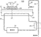
图1所示为一种抛光装置,可平整衬底上形成的绝缘层。如授予Seiichi Morimoto等人的美国专利NO.5,127,196所公开的名为“平整半导体衬底上形成的介质层的装置”。抛光装置100包括一工作台20,一半导体衬底23,一挂架24,一热交换器26,第一和第二导管32和36,一制冷单元35和一管嘴38。在抛光装置100中,半导体衬底23在平整时面朝下置于工作台20上。工作台20包括一个固定地贴附在其顶面的一衬垫21。衬垫21由多孔材料制成,与半导体衬底23上形成的介质层的上表面相接。多孔材料可吸收微粒物质,例如二氧化硅或其它研磨材料。Figure 1 shows a polishing device that can level the insulating layer formed on the substrate. As disclosed in U.S. Patent No. 5,127,196 to Seiichi Morimoto et al., entitled "Apparatus for Flattening a Dielectric Layer Formed on a Semiconductor Substrate". The
挂架24用来施加一向下的压力F1,作用于半导体衬底23的背部,衬底通过真空或仅通过湿表面张力与挂架24底部相接。还可设一嵌垫30,在半导体衬底23和挂架24之间起缓冲作用。一普通挡圈29用于防止半导体衬底23横向滑离挂架24。所施加的向下压力F1,一般为5磅每平方英寸的数量级,通过接在挂架24背部的轴27施加。此压力用于促进介质层上表面的研磨抛光。The
同时,制冷单元35使冷却剂在流过第一导管32时冷却。第一导管32通过工作台20的内部以使工作台20的温度在抛光过程中可降至室温以下。在抛光装置100中,冷却剂包括普通的水,由制冷单元35控制其温度,以使工作台20的温度在整个抛光加工过程中保持在10度左右。制冷单元35还提供有使冷却剂循环通过第一导管32和工作台20的装置。At the same time, the
第二导管36在抛光处理过程中将研磨材料传输至衬垫21的表面。研磨材料最好由一种名为“浆液”的悬浮液来传输,以利于抛光加工。浆液经由第二导管36抽吸后,通过管嘴38被导向衬垫21的表面。The
在操作过程中,挂架24相对于工作台20典型地以圆周运动方式旋转。此旋转运动通常由将一个普通电机连接到轴27上达到。并且,工作台20由公知机械装置来转动,以使抛光装置100平整在半导体衬底23上形成的介质层。During operation,
上述抛光装置的主要缺点之一在于,它不易精确控制其上被抛光的介质层的厚度,因为,它还需精确控制抛光时间和所施加的压力。One of the main disadvantages of the above-mentioned polishing device is that it is not easy to precisely control the thickness of the dielectric layer being polished thereon, because it also needs to precisely control the polishing time and the applied pressure.
本发明的主要目的是提供一种能够控制被抛光的介质层的厚度的装置。The main object of the present invention is to provide a device capable of controlling the thickness of the dielectric layer being polished.
根据本发明提供了一种可在抛光过程中,精确控制沉积于半导体衬底顶面的介质层的厚度的抛光装置。它包括:一具有一顶面和一底面的工作台,所述的顶面具有可吸收微粒物质的多孔材料;半导体衬底的夹持装置,其中,所述的夹持装置包括一具有一顶面和一底面的挂架,一连接于挂架顶面的轴,一贴附于挂架底面的嵌垫和一沿底面外沿连接的挡圈,可夹持半导体衬底;将夹持装置移向工作台顶面的装置,并可在预定位置锁定夹持装置,从而使介质层置于工作台顶面以上的预定位置;向工作台顶面传输研磨材料的装置;使夹持装置旋转的装置,以使研磨材料和介质层之间产生摩擦;控制工作台的垂直方向位置的装置,其中所述的垂直方向位置控制装置与工作台底面相接;一空腔用以围绕垂直方向位置控制装置,其中所述的空腔由绝热材料制成,从而使空腔内的温度保持恒定。According to the invention, a polishing device which can accurately control the thickness of the dielectric layer deposited on the top surface of the semiconductor substrate during the polishing process is provided. It includes: a workbench with a top surface and a bottom surface, the top surface has a porous material that can absorb particulate matter; a clamping device for a semiconductor substrate, wherein the clamping device includes a workbench with a top surface A hanger on the top surface and a bottom surface, a shaft connected to the top surface of the hanger, an inlay pad attached to the bottom surface of the hanger and a retaining ring connected along the outer edge of the bottom surface can clamp the semiconductor substrate; the clamping device A device that moves toward the top of the table and locks the clamping device at a predetermined position so that the media layer is placed at a predetermined position above the top of the table; a device that transfers abrasive material to the top of the table; rotates the clamping device A device for friction between the grinding material and the medium layer; a device for controlling the vertical position of the workbench, wherein the vertical position control device is connected to the bottom surface of the workbench; a cavity is used to surround the vertical position control A device wherein said cavity is made of a thermally insulating material such that the temperature within the cavity is kept constant.
在以下结合附图对较佳实施例的描述中,将体现出本发明的上述和其它目的及优点,其中:In the following description of the preferred embodiments in conjunction with the accompanying drawings, the above-mentioned and other objects and advantages of the present invention will be manifested, wherein:
图1代表现有技术的抛光装置的示意图。Figure 1 represents a schematic diagram of a prior art polishing apparatus.
图2提供了根据本发明的抛光装置的示意图。Figure 2 provides a schematic illustration of a polishing apparatus according to the present invention.
图3描绘了介质层沉积后的半导体衬底的断面图。Fig. 3 depicts a cross-sectional view of a semiconductor substrate after deposition of a dielectric layer.
图4表示根据本发明的抛光处理后的半导体衬底的断面图。Fig. 4 shows a cross-sectional view of a polished semiconductor substrate according to the present invention.
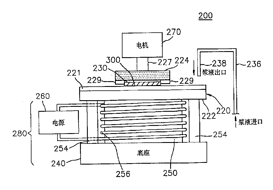
如图2,示出了根据本发明较佳实施例所述的抛光衬底上形成的介质层的装置。FIG. 2 shows an apparatus for polishing a dielectric layer formed on a substrate according to a preferred embodiment of the present invention.
抛光装置200由一具有一顶面和一底面221,222的工作220,和一用以夹持一半导体衬底300的挂架224所组成。该挂架224包括一挡圈229,一嵌垫230,一导管236,一管嘴238,和一驱动总成280,它包括一底座240,一热延伸材料250,一空腔254,一加热盘管256和一电源260。The
在抛光装置200中,半导体衬底300在抛光处理时面朝下置于工作台220上。工作台220的顶面221由多孔材料制成,与半导体衬底300形成的介质层相接触。多孔材料可吸收微粒物质,例如二氧化硅或其它研磨材料。In the
半导体衬底300由具有一顶面和一底面的挂架24夹持。半导体衬底300通过真空或湿表面张力贴附于挂架224底面。挡圈229连接在挂架224底面外沿,以防止半导体衬底300横向滑离挂架224。嵌垫230贴附于挂架224底面的中心部位,在半导体衬底300和挂架224之间起缓冲作用。一轴227将挂架224的顶面与一电机270相连,以使挂架224可以预定位置沿轴227移向工作台220的顶面221。随后,由公知机械装置(未示出)将挂架224锁定于预定位置。The
同时,在抛光处理时,导管236将研磨材料传输至工作台220的顶面221。此研磨材料最好由一种名为“浆液”的悬浮液来传输,以利于抛光处理。经由导管236抽吸后,浆液通过管嘴238被导引至工作台220的顶面221。Meanwhile, during the polishing process, the
在操作过程中,挂架224相对于工作台220典型地以圆周运动方式旋转,从而在研磨材料和介质层之间产生摩擦。此旋转运动通常由与轴227相连的电机270来驱动。During operation,
驱动总成280与工作台220的底面222相连接,控制工作台220的垂直方向运动。热延伸材料250设置在底座240和工作台220的底面222之间。图3中的标记h表示将由抛光装置200抛光掉的介质层部分。The
后附的表格绘制了工作台220的垂直方向运动和热延伸材料250之间的关系。如果热延伸材料由锆(Zr)制成,热延伸材料250的厚度是1cm,则温度每变化一度,工作台220移动420埃()。The accompanying table plots the relationship between the vertical motion of the table 220 and the thermally extended
电源260与加热盘管256相连接,向加热盘管供电,以使加热盘管256加热热延伸材料250。因此,热延伸材料250延伸与加热盘管256所供之热量对应的量。热延伸材料250由绝热材料制成的空腔254围绕,以防止热量散发,保持空腔254内温度恒定。The
图3所示为抛光处理前,绝缘层330沉积后的半导体衬底的断面图。金属线320位于衬底310的平顶面上。金属线320由常规的光刻法形成。下一步,介质层330,例如由氧化硅制成的,在金属线320的顶部形成;而衬底310则使用例如化学汽相淀积法形成。介质层330的厚度最好大于金属线320的厚度。因金属线320位于衬底310的顶面,所形成的介质层330不会是平的。相应于金属线320的部位,介质层会有一轻微的凸起。因此,实际应用前介质层330必须抛光。标记h表示将被本装置抛光掉的绝缘层部分。FIG. 3 is a cross-sectional view of a semiconductor substrate after deposition of an
如图4,为图3所示的半导体衬底300依据本发明的抛光处理后的断面图。FIG. 4 is a cross-sectional view of the
与现有技术的抛光装置相比,本发明的装置包括一驱动总成280,可精确控制200的垂直方向位置,因此控制了抛光的介质层的厚度。这可通过利用热延伸材料250来完成。Compared with the polishing device in the prior art, the device of the present invention includes a driving
通过对较佳实施例的图示和描述已示出了本发明,对所属技术领域的技术人员而言,在不脱离如所附的权利要求所述的本发明的精神和范围的情况下可作出多种变化和修改。Having shown and described the present invention by way of the preferred embodiment, it will be obvious to those skilled in the art without departing from the spirit and scope of the present invention as set forth in the appended claims. Various changes and modifications were made.
表 格
Claims (7)
Applications Claiming Priority (2)
| Application Number | Priority Date | Filing Date | Title |
|---|---|---|---|
| KR1019950002765A KR100258802B1 (en) | 1995-02-15 | 1995-02-15 | Flattening device and flattening method using the same |
| KR2765/1995 | 1995-02-15 |
Publications (2)
| Publication Number | Publication Date |
|---|---|
| CN1132676A CN1132676A (en) | 1996-10-09 |
| CN1073911C true CN1073911C (en) | 2001-10-31 |
Family
ID=19408152
Family Applications (1)
| Application Number | Title | Priority Date | Filing Date |
|---|---|---|---|
| CN95120467A Expired - Fee Related CN1073911C (en) | 1995-02-15 | 1995-12-08 | Apparatus for polishing dielectric layer formed on substrate |
Country Status (5)
| Country | Link |
|---|---|
| US (1) | US5664986A (en) |
| JP (1) | JP2969071B2 (en) |
| KR (1) | KR100258802B1 (en) |
| CN (1) | CN1073911C (en) |
| IN (1) | IN185476B (en) |
Families Citing this family (20)
| Publication number | Priority date | Publication date | Assignee | Title |
|---|---|---|---|---|
| US6083839A (en) * | 1997-12-31 | 2000-07-04 | Intel Corporation | Unique chemical mechanical planarization approach which utilizes magnetic slurry for polish and magnetic fields for process control |
| KR100413493B1 (en) * | 2001-10-17 | 2004-01-03 | 주식회사 하이닉스반도체 | Polishing Platen of Chemical Mechanical Polishing Equipment and method for plating |
| KR100835517B1 (en) | 2003-12-26 | 2008-06-04 | 동부일렉트로닉스 주식회사 | Platen device of CMP equipment |
| US7198548B1 (en) * | 2005-09-30 | 2007-04-03 | Applied Materials, Inc. | Polishing apparatus and method with direct load platen |
| CN103029031A (en) * | 2011-09-30 | 2013-04-10 | 上海双明光学科技有限公司 | Processing method for wafer substrates |
| CN103639886A (en) * | 2013-11-29 | 2014-03-19 | 上海华力微电子有限公司 | Mechanical machine grinding device and method for W-CMP |
| US9873180B2 (en) | 2014-10-17 | 2018-01-23 | Applied Materials, Inc. | CMP pad construction with composite material properties using additive manufacturing processes |
| US10875153B2 (en) | 2014-10-17 | 2020-12-29 | Applied Materials, Inc. | Advanced polishing pad materials and formulations |
| US11745302B2 (en) | 2014-10-17 | 2023-09-05 | Applied Materials, Inc. | Methods and precursor formulations for forming advanced polishing pads by use of an additive manufacturing process |
| SG11201703114QA (en) | 2014-10-17 | 2017-06-29 | Applied Materials Inc | Cmp pad construction with composite material properties using additive manufacturing processes |
| US9776361B2 (en) | 2014-10-17 | 2017-10-03 | Applied Materials, Inc. | Polishing articles and integrated system and methods for manufacturing chemical mechanical polishing articles |
| JP2016090439A (en) * | 2014-11-06 | 2016-05-23 | 株式会社日本自動車部品総合研究所 | Particle-like substance detection element and particle-like substance detection sensor |
| KR20230169424A (en) | 2015-10-30 | 2023-12-15 | 어플라이드 머티어리얼스, 인코포레이티드 | An apparatus and method of forming a polishing article that has a desired zeta potential |
| US10593574B2 (en) | 2015-11-06 | 2020-03-17 | Applied Materials, Inc. | Techniques for combining CMP process tracking data with 3D printed CMP consumables |
| US10391605B2 (en) | 2016-01-19 | 2019-08-27 | Applied Materials, Inc. | Method and apparatus for forming porous advanced polishing pads using an additive manufacturing process |
| US11471999B2 (en) | 2017-07-26 | 2022-10-18 | Applied Materials, Inc. | Integrated abrasive polishing pads and manufacturing methods |
| WO2019032286A1 (en) | 2017-08-07 | 2019-02-14 | Applied Materials, Inc. | Abrasive delivery polishing pads and manufacturing methods thereof |
| KR20210042171A (en) | 2018-09-04 | 2021-04-16 | 어플라이드 머티어리얼스, 인코포레이티드 | Formulations for advanced polishing pads |
| CN112605847B (en) * | 2020-11-23 | 2022-04-19 | 福建晶安光电有限公司 | Improved wafer substrate polishing method and apparatus |
| US11878389B2 (en) | 2021-02-10 | 2024-01-23 | Applied Materials, Inc. | Structures formed using an additive manufacturing process for regenerating surface texture in situ |
Citations (2)
| Publication number | Priority date | Publication date | Assignee | Title |
|---|---|---|---|---|
| EP0197214A2 (en) * | 1985-04-08 | 1986-10-15 | Rodel, Inc. | Carrier assembly for two-sided polishing operation |
| US5103596A (en) * | 1990-11-05 | 1992-04-14 | Toshiba Kikai Kabushiki Kaisha | Method and apparatus for controlling cylinder grinding machines |
Family Cites Families (5)
| Publication number | Priority date | Publication date | Assignee | Title |
|---|---|---|---|---|
| US3948089A (en) * | 1973-10-12 | 1976-04-06 | Westinghouse Electric Corporation | Strain gauge apparatus |
| NO135390C (en) * | 1975-09-02 | 1977-03-30 | Rdal Og Sunndal Verk A S | ELECTRIC STOVE WITH THERMOSTAT. |
| CA2012878C (en) * | 1989-03-24 | 1995-09-12 | Masanori Nishiguchi | Apparatus for grinding semiconductor wafer |
| US5127196A (en) * | 1990-03-01 | 1992-07-07 | Intel Corporation | Apparatus for planarizing a dielectric formed over a semiconductor substrate |
| DE69333322T2 (en) * | 1992-09-24 | 2004-09-30 | Ebara Corp. | polisher |
-
1995
- 1995-02-15 KR KR1019950002765A patent/KR100258802B1/en not_active Expired - Fee Related
- 1995-11-27 US US08/563,170 patent/US5664986A/en not_active Expired - Fee Related
- 1995-11-30 JP JP33578495A patent/JP2969071B2/en not_active Expired - Lifetime
- 1995-11-30 IN IN1546CA1995 patent/IN185476B/en unknown
- 1995-12-08 CN CN95120467A patent/CN1073911C/en not_active Expired - Fee Related
Patent Citations (2)
| Publication number | Priority date | Publication date | Assignee | Title |
|---|---|---|---|---|
| EP0197214A2 (en) * | 1985-04-08 | 1986-10-15 | Rodel, Inc. | Carrier assembly for two-sided polishing operation |
| US5103596A (en) * | 1990-11-05 | 1992-04-14 | Toshiba Kikai Kabushiki Kaisha | Method and apparatus for controlling cylinder grinding machines |
Also Published As
| Publication number | Publication date |
|---|---|
| IN185476B (en) | 2001-02-03 |
| KR100258802B1 (en) | 2000-06-15 |
| US5664986A (en) | 1997-09-09 |
| CN1132676A (en) | 1996-10-09 |
| JPH08229806A (en) | 1996-09-10 |
| JP2969071B2 (en) | 1999-11-02 |
| KR960032635A (en) | 1996-09-17 |
Similar Documents
| Publication | Publication Date | Title |
|---|---|---|
| CN1073911C (en) | Apparatus for polishing dielectric layer formed on substrate | |
| US6315635B1 (en) | Method and apparatus for slurry temperature control in a polishing process | |
| JP4567195B2 (en) | Conditioner for chemical mechanical polishing | |
| CN111512425A (en) | Temperature control for chemical mechanical polishing | |
| US6257954B1 (en) | Apparatus and process for high temperature wafer edge polishing | |
| US12311495B2 (en) | Temperature control in chemical mechanical polish | |
| JP2002514517A (en) | Carrier head with retaining ring for use in chemical / mechanical polishing systems | |
| JP7106209B2 (en) | SiC substrate polishing method | |
| JPH11262856A (en) | Holding device for planar object | |
| CN117484291A (en) | Ultrasonic vibration auxiliary polishing device | |
| US6402597B1 (en) | Polishing apparatus and method | |
| CN1685473A (en) | Electrostatic chuck with low level particle generation and method of making the same | |
| US20210305080A1 (en) | Wafer surface processing device | |
| US20020016136A1 (en) | Conditioner for polishing pads | |
| JPH1029153A (en) | Semiconductor wafer polishing equipment | |
| JP7797424B2 (en) | Semiconductor substrate polishing with polishing pad temperature control | |
| KR20060038740A (en) | Chemical mechanical polishing apparatus and polishing method using the apparatus | |
| JPH0724708A (en) | Polishing method and polishing apparatus | |
| JP6606017B2 (en) | Substrate processing equipment | |
| KR100348929B1 (en) | Polish pressure modulation in cmp to preferentially polish raised features | |
| JP2000354958A (en) | Work polishing apparatus, work polishing method, and semiconductor device manufacturing method | |
| JPH02240925A (en) | Wafer polishing equipment | |
| JPH03278434A (en) | Polishing holder for semiconductor wafer | |
| CN222606871U (en) | Valve sealing face hardening processing equipment | |
| US20260070182A1 (en) | Chemical mechanical planarization apparatus and method |
Legal Events
| Date | Code | Title | Description |
|---|---|---|---|
| C06 | Publication | ||
| PB01 | Publication | ||
| C10 | Entry into substantive examination | ||
| SE01 | Entry into force of request for substantive examination | ||
| C14 | Grant of patent or utility model | ||
| GR01 | Patent grant | ||
| C19 | Lapse of patent right due to non-payment of the annual fee | ||
| CF01 | Termination of patent right due to non-payment of annual fee | ||
| REG | Reference to a national code |
Ref country code: HK Ref legal event code: GR Ref document number: 1028746 Country of ref document: HK |