CN103748566A - An innovative structure for the register group - Google Patents
An innovative structure for the register group Download PDFInfo
- Publication number
- CN103748566A CN103748566A CN201180071429.4A CN201180071429A CN103748566A CN 103748566 A CN103748566 A CN 103748566A CN 201180071429 A CN201180071429 A CN 201180071429A CN 103748566 A CN103748566 A CN 103748566A
- Authority
- CN
- China
- Prior art keywords
- register
- module
- request
- address
- target
- Prior art date
- Legal status (The legal status is an assumption and is not a legal conclusion. Google has not performed a legal analysis and makes no representation as to the accuracy of the status listed.)
- Pending
Links
Images


Classifications
-
- G—PHYSICS
- G06—COMPUTING OR CALCULATING; COUNTING
- G06F—ELECTRIC DIGITAL DATA PROCESSING
- G06F13/00—Interconnection of, or transfer of information or other signals between, memories, input/output devices or central processing units
- G06F13/38—Information transfer, e.g. on bus
- G06F13/40—Bus structure
- G06F13/4063—Device-to-bus coupling
-
- G—PHYSICS
- G06—COMPUTING OR CALCULATING; COUNTING
- G06F—ELECTRIC DIGITAL DATA PROCESSING
- G06F13/00—Interconnection of, or transfer of information or other signals between, memories, input/output devices or central processing units
- G06F13/38—Information transfer, e.g. on bus
- G06F13/42—Bus transfer protocol, e.g. handshake; Synchronisation
- G06F13/4247—Bus transfer protocol, e.g. handshake; Synchronisation on a daisy chain bus
-
- Y—GENERAL TAGGING OF NEW TECHNOLOGICAL DEVELOPMENTS; GENERAL TAGGING OF CROSS-SECTIONAL TECHNOLOGIES SPANNING OVER SEVERAL SECTIONS OF THE IPC; TECHNICAL SUBJECTS COVERED BY FORMER USPC CROSS-REFERENCE ART COLLECTIONS [XRACs] AND DIGESTS
- Y02—TECHNOLOGIES OR APPLICATIONS FOR MITIGATION OR ADAPTATION AGAINST CLIMATE CHANGE
- Y02D—CLIMATE CHANGE MITIGATION TECHNOLOGIES IN INFORMATION AND COMMUNICATION TECHNOLOGIES [ICT], I.E. INFORMATION AND COMMUNICATION TECHNOLOGIES AIMING AT THE REDUCTION OF THEIR OWN ENERGY USE
- Y02D10/00—Energy efficient computing, e.g. low power processors, power management or thermal management
Landscapes
- Engineering & Computer Science (AREA)
- Theoretical Computer Science (AREA)
- General Engineering & Computer Science (AREA)
- Physics & Mathematics (AREA)
- General Physics & Mathematics (AREA)
- Computer Hardware Design (AREA)
- Advance Control (AREA)
- Information Transfer Systems (AREA)
Abstract
Description
技术领域 technical field
本发明一般涉及处理电路架构,并且更具体地说,涉及用于具有串联连接以形成模块流水线的多个模块的处理电路的流水线架构。 The present invention relates generally to processing circuit architectures, and more particularly to pipeline architectures for processing circuits having a plurality of modules connected in series to form a pipeline of modules.
背景技术 Background technique
用于移动终端或其它装置的处理电路可实现为专用集成电路(ASIC)或现场可编程门阵列(FPGA),其中,不同的功能由不同的模块实现。不同功能在不同模块中的实现使得能够更新或替换一个模块而不影响其它模块的功能。模块用于实现其指派的功能的配置数据、状态信息及其它数据存储在寄存器中。使用用于存储配置数据的寄存器使得模块能够在多种模式中操作和执行多个功能。 Processing circuits for mobile terminals or other devices may be implemented as Application Specific Integrated Circuits (ASICs) or Field Programmable Gate Arrays (FPGAs), where different functions are implemented by different modules. Implementation of different functions in different modules enables one module to be updated or replaced without affecting the functionality of other modules. Configuration data, status information, and other data that a module uses to carry out its assigned functions are stored in registers. Using registers to store configuration data enables the module to operate in multiple modes and perform multiple functions.
寄存器在处理电路中的组织是一个设计考虑事项。组织寄存器的一种常规方案是在寄存器单元中集中所有寄存器。每个模块直接被接口于匹配的寄存器。寄存器单元负责将寄存器地址解码并且将存储的值输出到对应模块。 The organization of registers in the processing circuitry is a design consideration. A conventional scheme for organizing registers is to centralize all registers in register cells. Each module is directly interfaced to matching registers. The register unit is responsible for decoding the register address and outputting the stored value to the corresponding module.
此集中式方案具有几个缺点。例如,集中式解决方案要求寄存器单元将所有寄存器地址解码,这通常要求复杂的逻辑并且因此导致定时问题。此外,由于寄存器单元负责将所有寄存器分布到模块,因此,它需要与所有模块进行接口。此一对多接口可导致在寄存器模块组的路由选择拥塞。另外,此解决方案难以更新。例如,如果添加或去除新模块,则要修正寄存器单元和对应逻辑。 This centralized approach has several disadvantages. For example, centralized solutions require register units to decode all register addresses, which typically requires complex logic and thus leads to timing issues. Also, since the register unit is responsible for distributing all registers to modules, it needs to interface with all modules. This one-to-many interface can cause routing congestion in the register block. Also, this solution is difficult to update. For example, if new blocks are added or removed, the register cells and corresponding logic are revised.
组织寄存器的另一常规方案是在连接到内部寄存器总线的模块之间分布寄存器。在此方案中,每个模块包括其自己的寄存器组和解码器,并且连接到内部寄存器总线。总线转换器提供到寄存器总线的外部接口,并且将外部接口协议转换成内部寄存器总线协议。所有模块同时监视内部寄存器总线。在断定有寄存器请求时,所有模块将与寄存器请求相关联的目标寄存器地址解码。如果目标寄存器地址指定属于模块的寄存器,则模块将寄存器数据锁存到指定寄存器,或者从其读取寄存器数据。所有其它模块不进行任何操作。 Another conventional scheme for organizing registers is to distribute registers among modules connected to an internal register bus. In this scheme, each block includes its own register set and decoder, and is connected to an internal register bus. The bus converter provides an external interface to the register bus and converts the external interface protocol to the internal register bus protocol. All modules simultaneously monitor the internal register bus. Upon asserting a register request, all modules decode the target register address associated with the register request. If the target register address specifies a register belonging to the module, the module latches the register data into the specified register, or reads the register data from it. All other modules do nothing.
虽然内部总线结构消除了与集中式寄存器解决方案相关联的一对多接口和更新问题,但总线结构解决方案将遇到定时问题。具体而言,随着与内部寄存器总线进行接口的模块数量增大,寄存器总线的扇出(fan-out)极高,这产生了大的定时延迟。 While the internal bus structure eliminates the one-to-many interface and update issues associated with centralized register solutions, the bus-structured solution suffers from timing issues. Specifically, as the number of modules interfacing with the internal register bus increases, the fan-out of the register bus is extremely high, which creates large timing delays.
因此,仍需要消除或降低与常规方案相关联的定时问题的改进的处理电路架构。 Accordingly, there remains a need for improved processing circuit architectures that eliminate or reduce timing issues associated with conventional approaches.
发明内容 Contents of the invention
一种处理电路包括经多个寄存器总线段串联连接以形成模块流水线的多个模块。每个模块包括一个或多个寄存器,并且指派有对应的地址范围。包括目标寄存器地址的寄存器请求从一个模块沿模块流水线向下传递到后一模块,直至在包含目标寄存器的模块接收到寄存器请求。 A processing circuit includes a plurality of modules connected in series via a plurality of register bus segments to form a pipeline of modules. Each module includes one or more registers and is assigned a corresponding address range. A register request including a target register address is passed down the module pipeline from one module to a subsequent module until the register request is received at the module containing the target register.
本发明的示范实施例包括由模块流水线中与多个类似模块连接的处理模块所实现的方法。在一种示范方法中,通过经内部寄存器总线的第一段连接到前一模块的第一接口,接收包括目标寄存器地址的寄存器请求。比较目标寄存器地址和处理模块的地址范围。如果目标寄存器地址落在处理模块的地址范围内,则访问处理模块中的匹配寄存器以将数据写入匹配寄存器或者从其读取数据。如果目标寄存器地址落在处理模块的寄存器地址范围外,则将寄存器请求通过第二接口输出到经内部寄存器总线的第二段连接到处理模块的后一模块。 Exemplary embodiments of the invention include methods implemented by a processing module connected to a plurality of similar modules in a pipeline of modules. In one exemplary method, a register request including a target register address is received via a first interface connected to a previous module via a first segment of the internal register bus. Compare the target register address with the address range of the processing module. If the target register address falls within the address range of the processing module, a matching register in the processing module is accessed to write data to or read data from the matching register. If the target register address falls outside the register address range of the processing module, the register request is output through the second interface to a subsequent module connected to the processing module via the second segment of the internal register bus.
本发明的其它示范实施例包括一种连接到多个类似模块以形成模块流水线的处理电路中的处理模块。一种示范处理模块包括第一接口、第二接口、用于存储数据的一个或多个寄存器及解码器。第一接口经内部寄存器总线的第一段连接到前一模块。第二接口经内部寄存器总线的第二段连接到后一模块。解码器配置成通过第一接口接收寄存器请求,并且比较与寄存器请求相关联的目标寄存器地址和用于处理模块的地址范围。如果目标寄存器地址落在寄存器地址范围内,则解码器访问处理模块中的匹配寄存器以将数据写入匹配寄存器或者从其读取数据。如果目标寄存器地址落在处理模块的地址范围外,则解码器通过第二接口将寄存器请求输出到后一模块。 Other exemplary embodiments of the invention include a processing module in a processing circuit connected to a plurality of similar modules to form a pipeline of modules. An exemplary processing module includes a first interface, a second interface, one or more registers for storing data, and a decoder. The first interface is connected to the previous module via the first segment of the internal register bus. The second interface is connected to the latter module via the second segment of the internal register bus. The decoder is configured to receive a register request via the first interface, and compare a target register address associated with the register request with an address range for the processing module. If the target register address falls within the register address range, the decoder accesses a match register in the processing module to write data to or read data from the match register. If the target register address falls outside the address range of the processing module, the decoder outputs the register request to the latter module through the second interface.
本发明的其它实施例包括一种具有连接以形成模块流水线的多个模块的处理电路所实现的方法。在一种示范方法中,按顺序通过经内部寄存器总线串联连接的多个模块传递包括目标寄存器地址的寄存器请求。内部寄存器总线包括连接相邻模块的多个段。在接收寄存器请求的每个模块,比较目标寄存器地址和接收模块的地址范围。如果目标寄存器地址落在接收模块的地址范围内,则访问接收模块内的匹配寄存器以将数据写入匹配寄存器或者从其读取数据。如果目标寄存器地址落在接收模块的地址范围外,并且如果有后一模块,则通过内部寄存器总线将寄存器请求传递到后一模块。 Other embodiments of the invention include a method implemented by a processing circuit having a plurality of modules connected to form a pipeline of modules. In one exemplary approach, a register request including a target register address is passed sequentially through a plurality of modules connected in series via an internal register bus. The internal register bus consists of multiple segments connecting adjacent blocks. At each module that receives a register request, compare the target register address to the address range of the receiving module. If the target register address falls within the address range of the receiving module, a match register within the receiving module is accessed to write data to or read data from the matching register. If the target register address falls outside the address range of the receiving module, and if there is a latter module, the register request is passed to the latter module through the internal register bus.
本发明的其它实施例包括带有流水线架构的处理电路。在一个实施例中,处理电路包括多个模块、具有串联连接多个模块以形成模块流水线的两个或更多段的内部寄存器总线及用于每个模块的解码器。每个模块包括一个或多个寄存器。内部寄存器总线配置成通过串联连接的模块传递包括目标寄存器地址的寄存器请求。用于接收模块的解码器配置成比较目标寄存器地址和用于接收模块的寄存器地址范围。如果目标寄存器地址落在接收模块的寄存器地址范围内,则接收模块内的匹配寄存器将数据写入匹配寄存器或者从其读取数据。如果目标寄存器地址落在接收模块的寄存器地址范围外,并且如果有后一模块,则解码器将寄存器请求传递到后一模块。 Other embodiments of the invention include processing circuits with pipelined architectures. In one embodiment, a processing circuit includes a plurality of modules, an internal register bus having two or more stages connecting the plurality of modules in series to form a module pipeline, and a decoder for each module. Each module includes one or more registers. The internal register bus is configured to communicate register requests including target register addresses through the serially connected modules. The decoder for the receiving module is configured to compare the target register address to a range of register addresses for the receiving module. A match register within the receive module writes data to or reads data from the match register if the target register address falls within the register address range of the receive module. If the target register address falls outside the register address range of the receiving module, and if there is a latter module, the decoder passes the register request to the latter module.
与常规解决方案相比,本文中所述流水线架构和技术提供了改进的定时性能。此外,通过修改现有模块或者添加新模块到流水线,更轻松扩展处理电路。由于寄存器在相应模块内实现,因此,对一个模块的修改不会影响其它模块。 The pipeline architecture and techniques described herein provide improved timing performance compared to conventional solutions. In addition, it is easier to expand the processing circuitry by modifying existing modules or adding new modules to the pipeline. Since the registers are implemented within the corresponding modules, modifications to one module do not affect other modules.
附图说明 Description of drawings
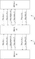
图1示出根据一个示范实施例的具有串联连接的模块的处理电路的框图。 FIG. 1 shows a block diagram of a processing circuit with modules connected in series, according to an exemplary embodiment.
图2示出用于图1的可配置电路的示范模块的框图。 FIG. 2 shows a block diagram of exemplary modules for the configurable circuit of FIG. 1 .
图3示出由模块执行的示范方法。 Figure 3 illustrates an exemplary method performed by the modules.
图4示出在三个模块之间的示范接口图。 Figure 4 shows an exemplary interface diagram between the three modules.
图5示出由模块执行的另一示范方法。 Figure 5 illustrates another exemplary method performed by a module.
具体实施方式 Detailed ways
图1示出根据一个示范实施例的处理电路5。处理电路5例如可包括专用集成电路(ASIC)或现场可编程门阵列(FPGA)。处理电路5包括总线转换器10和多个模块20A-G。如下面将更详细描述的,每个模块20包括用于存储模块20使用的配置数据、状态信息或其它数据的一个或多个寄存器24(图2)。总线转换器10和模块20由内部寄存器总线30的段32串联连接。内部寄存器总线30的每段将一个模块20连接到前一模块20、后一模块20和/或总线转换器10以形成模块流水线。每个模块20也连接到数据总线40以接收要处理的数据和输出处理后的数据。示范实施例中示出了两个数据总线40。然而,本领域技术人员将领会,数据总线的数量对本发明不是决定性的。
Figure 1 shows a
总线转换器10提供到内部寄存器总线30的外部接口,以使得外部应用能够访问模块20内的寄存器。总线转换器10通过接口总线(未示出)接收来自外部应用的寄存器请求,并且将寄存器请求从在接口总线上使用的外部接口协议转换成在内部寄存器总线30上使用的内部寄存器总线协议。总线转换器10将转换的寄存器请求转发到模块流水线中的第一模块20A。如下面将更详细描述的,按顺序将寄存器请求从一个模块20传递到后一模块20,直至它到达包含目标寄存器的模块20。在接收寄存器请求时,接收模块20将目标寄存器地址解码,并且比较解码的地址和其指派的寄存器地址范围以确定目标寄存器是否属于接收模块20。如果目标寄存器地址落在接收模块20的寄存器地址范围内,则模块20将寄存器数据锁存到匹配寄存器(即,具有与目标寄存器地址匹配的寄存器地址的寄存器)中或者从其读取寄存器数据。如果目标寄存器地址落在接收模块20的寄存器地址范围外,则接收模块20将寄存器请求传递到后一模块20。
图2示出示范模块20的主要功能组件。模块20包括寄存器组22、控制器26和数据处理单元28。寄存器组22包括解码器23和一个或多个寄存器24。寄存器24存储由模块20使用的配置信息、状态信息或其它信息。如下文描述的,解码器23将与模块20接收的寄存器请求相关联的目标寄存器地址解码。控制器26控制模块20的操作,并且为数据处理单元28提供寄存器组22中的寄存器24的访问权。数据处理单元28执行指派到模块20的处理功能。数据处理单元28可执行不同的功能或者在不同模式中操作,这取决于寄存器24中存储的配置数据。也就是说,通过将配置数据写入寄存器24中,能够控制数据处理单元28的功能或模式。
FIG. 2 shows the main functional components of the
寄存器组22内的每个寄存器24具有在用于主机模块20的预定的寄存器地址范围内的对应寄存器地址。将领会的是,模块20的寄存器地址范围包括指派到模块20内寄存器24的一个或多个地址,并且寄存器地址范围可以是连续或非连续的。寄存器组22具有经一个内部总路线段32连接到前一模块20或总线转换器10的第一接口21A和经另一内部总线段32连接到后一模块20的第二接口21B。第二接口21B未由例如模块20G等在模块流水线中的最后模块20使用。图4中示出并且下面更详细描述了第一和第二接口。
Each register 24 within
为了访问寄存器24,外部应用将寄存器请求发送到总线转换器10。总线转换器10将寄存器请求转换到内部寄存器总线协议,并且将转换的寄存器请求转发到第一模块20A。寄存器请求包括指定目标寄存器的目标寄存器地址。寄存器请求可包括写入请求或读取请求。寄存器请求由模块通过第一接口21A接收时,解码器23将与寄存器请求相关联的目标寄存器地址解码,并且比较目标寄存器地址和其寄存器24的地址范围和/或各个地址,以确定目标寄存器是否属于模块20。如果目标寄存器不属于模块20,则解码器23通过第二接口将寄存器请求输出到流水线中的后一模块20。如果目标寄存器属于模块20,则解码器23将写入数据锁存到目标寄存器中(写入请求),或者从目标寄存器读取寄存数据(读取请求)。
To access registers 24 , an external application sends a register request to
图3示出由处理模块20实现的示范过程100。处理模块20接收包括在经内部寄存器总线的第一段连接到前一模块20或总线转换器10的第一接口上目标寄存器地址的寄存器请求(框110),并且比较目标寄存器地址和用于接收模块20的寄存器地址范围(框120)。如果目标寄存器地址落在处理模块20的寄存器地址范围内,则解码器23访问匹配寄存器24以将数据写入匹配寄存器,或者从其读取数据(框130)。如果目标寄存器地址落在寄存器地址范围外,则解码器23将寄存器请求输出到经第二接口连接到处理模块20的后一模块20(框140)。
FIG. 3 illustrates an exemplary process 100 implemented by processing
图4示出在连接模块K到前一模块(模块K-1)和后一模块(模块K+1)的内部总线段中包含的示范接口。表1识别内部寄存器总线段32的各种行,其中,符号“?”表示“i”或“o”,其中,“i”指示用于模块K的输入信号,以及“o”指示用于模块K的输出信号。
Figure 4 shows an exemplary interface comprised in the internal bus segment connecting module K to the preceding module (module K-1) and the succeeding module (module K+1). Table 1 identifies the various rows of the internal
表1:内部寄存器总线接口 Table 1: Internal Register Bus Interface
内部寄存器总线接口包括6个接口。表1中列出的前4个接口将本文中所述寄存器请求提供到接收模块20,例如,写入/读取接口识别寄存器请求是读取请求还是写入请求,以及Reg_address接口携带目标寄存器地址。如本文中公开的,剩余的接口有利于读取的数据沿流水线向上传递。
The internal register bus interface includes 6 interfaces. The first 4 interfaces listed in Table 1 provide the register requests described herein to the receiving
图5公开由模块20(模块K)执行的另一示范方法200。模块K监视与前一模块20(模块K-1)或总线转换器10之间的接口,以确定何时接收寄存器请求(框210),其中,寄存器请求按顺序通过模块20传递。模块K接收寄存器请求时,模块K中的解码器23将请求的目标地址解码(框220)。如果解码的地址不在模块K的地址范围中(框230),则模块K将寄存器请求与任何相关联数据传递到后一模块20(模块K+1),以将寄存器请求和相关联数据沿模块流水线向下传递(框240)。然而,如果解码的地址在模块K的地址范围中(框230),则解码器230确定请求类型(框250)。如果寄存器请求是写入请求,则解码器23将与寄存器请求相关联的数据锁存到匹配寄存器(即,模块K中具有与目标寄存器地址匹配的寄存器地址的寄存器)中(框260)。如果寄存器请求是读取请求,则解码器23从匹配寄存器读取数据,并且将读取的数据发送到前一模块20(模块K-1),以将读取的数据沿模块流水线向上传递(框270)。在此情况下,每个模块20接收来自后一模块20的读取的数据,并且将接收的读取的数据输出到前一模块20,以将读取的数据沿模块流水线向上传递。
FIG. 5 discloses another exemplary method 200 performed by module 20 (module K). Module K monitors the interface with the previous module 20 (module K-1 ) or
本文中公开的处理电路5、模块20和对应方法100和200具有优于常规实现的几个益处,例如,更佳的定时性能、灵活的更新和降低的功耗。具体而言,由于每个模块20只将其自己的寄存器地址解码,并且内部寄存器总线被分段,因此,避免了常规解决方案的定时问题。此外,通过将新模块20连接到寄存器流水线的任何级,可添加新模块,而不要求对处理电路已经实现的逻辑功能进行任何修改。类似地,通过从寄存器流水线断开旧模块20,可从处理电路去除该旧模块。此外,由于大部分电路功率在切换内部寄存器时被消耗,并且由于使用本文中公开的流水线结构降低了寄存器切换速率(因为该流水线结构在寄存器请求到达包含目标寄存器的模块20时终止了该寄存器请求),因此,本文中公开的流水线结构降低了电路功耗。
The
当然,在不脱离本发明基本特性的情况下,本发明可以不同于本文具体所述那些方式外的其它方式中来实现。呈现的实施例在所有方面均要视为说明性的而不是限制性的,并且落在随附权利要求的意义和等同范围内的所有更改旨在被涵盖于其中。 The present invention may, of course, be carried out in other ways than those specifically set forth herein without departing from essential characteristics of the invention. The presented embodiments are to be considered in all respects as illustrative rather than restrictive, and all changes that come within the meaning and range of equivalency of the appended claims are intended to be embraced therein.
Claims (20)
Applications Claiming Priority (1)
| Application Number | Priority Date | Filing Date | Title |
|---|---|---|---|
| PCT/CN2011/000948 WO2012167396A1 (en) | 2011-06-07 | 2011-06-07 | An innovative structure for the register group |
Publications (1)
| Publication Number | Publication Date |
|---|---|
| CN103748566A true CN103748566A (en) | 2014-04-23 |
Family
ID=47295320
Family Applications (1)
| Application Number | Title | Priority Date | Filing Date |
|---|---|---|---|
| CN201180071429.4A Pending CN103748566A (en) | 2011-06-07 | 2011-06-07 | An innovative structure for the register group |
Country Status (4)
| Country | Link |
|---|---|
| US (1) | US20140173160A1 (en) |
| EP (1) | EP2718827B1 (en) |
| CN (1) | CN103748566A (en) |
| WO (1) | WO2012167396A1 (en) |
Cited By (2)
| Publication number | Priority date | Publication date | Assignee | Title |
|---|---|---|---|---|
| CN110046105A (en) * | 2019-04-26 | 2019-07-23 | 中国科学院微电子研究所 | A kind of 3D NAND Flash |
| CN112667354A (en) * | 2020-12-30 | 2021-04-16 | 上海壁仞智能科技有限公司 | Computer readable storage medium, virtualized register device, and method of accessing the device |
Families Citing this family (2)
| Publication number | Priority date | Publication date | Assignee | Title |
|---|---|---|---|---|
| US20160179726A1 (en) * | 2014-12-17 | 2016-06-23 | Qualcomm Incorporated | Programming hardware registers using a pipelined register bus, and related methods, systems, and apparatuses |
| US10628373B2 (en) * | 2015-12-01 | 2020-04-21 | Marvell International Ltd. | Systems and methods for transmitting an access request via a flexible register access bus |
Citations (3)
| Publication number | Priority date | Publication date | Assignee | Title |
|---|---|---|---|---|
| US6073233A (en) * | 1997-10-08 | 2000-06-06 | Cisco Technology, Inc. | Method and apparatus for distributing and accessing configuration registers |
| CN1858854A (en) * | 2005-12-28 | 2006-11-08 | 华为技术有限公司 | Register access device and method |
| US20070115292A1 (en) * | 2005-10-26 | 2007-05-24 | Via Technologies, Inc | GPU Internal Wait/Fence Synchronization Method and Apparatus |
Family Cites Families (4)
| Publication number | Priority date | Publication date | Assignee | Title |
|---|---|---|---|---|
| US4641308A (en) * | 1984-01-03 | 1987-02-03 | Texas Instruments Incorporated | Method of internal self-test of microprocessor using microcode |
| JP2004013504A (en) * | 2002-06-06 | 2004-01-15 | Univ Hiroshima | Pattern recognition system, associative memory device used in this system, and pattern recognition processing method |
| US8725991B2 (en) * | 2007-09-12 | 2014-05-13 | Qualcomm Incorporated | Register file system and method for pipelined processing |
| US7737725B1 (en) * | 2008-04-04 | 2010-06-15 | Xilinx, Inc. | Device control register for a processor block |
-
2011
- 2011-06-07 CN CN201180071429.4A patent/CN103748566A/en active Pending
- 2011-06-07 EP EP11867381.3A patent/EP2718827B1/en not_active Not-in-force
- 2011-06-07 WO PCT/CN2011/000948 patent/WO2012167396A1/en not_active Ceased
- 2011-06-07 US US14/123,810 patent/US20140173160A1/en not_active Abandoned
Patent Citations (3)
| Publication number | Priority date | Publication date | Assignee | Title |
|---|---|---|---|---|
| US6073233A (en) * | 1997-10-08 | 2000-06-06 | Cisco Technology, Inc. | Method and apparatus for distributing and accessing configuration registers |
| US20070115292A1 (en) * | 2005-10-26 | 2007-05-24 | Via Technologies, Inc | GPU Internal Wait/Fence Synchronization Method and Apparatus |
| CN1858854A (en) * | 2005-12-28 | 2006-11-08 | 华为技术有限公司 | Register access device and method |
Cited By (4)
| Publication number | Priority date | Publication date | Assignee | Title |
|---|---|---|---|---|
| CN110046105A (en) * | 2019-04-26 | 2019-07-23 | 中国科学院微电子研究所 | A kind of 3D NAND Flash |
| CN110046105B (en) * | 2019-04-26 | 2021-10-22 | 中国科学院微电子研究所 | A 3D NAND Flash |
| CN112667354A (en) * | 2020-12-30 | 2021-04-16 | 上海壁仞智能科技有限公司 | Computer readable storage medium, virtualized register device, and method of accessing the device |
| CN112667354B (en) * | 2020-12-30 | 2022-05-06 | 上海壁仞智能科技有限公司 | Computer-readable storage medium, virtualized register device, and method of accessing the same |
Also Published As
| Publication number | Publication date |
|---|---|
| WO2012167396A1 (en) | 2012-12-13 |
| US20140173160A1 (en) | 2014-06-19 |
| EP2718827A1 (en) | 2014-04-16 |
| EP2718827B1 (en) | 2016-08-10 |
| EP2718827A4 (en) | 2014-09-10 |
Similar Documents
| Publication | Publication Date | Title |
|---|---|---|
| US9385032B2 (en) | Systems and methods involving data bus inversion memory circuitry, configuration and/or operation | |
| US9032162B1 (en) | Systems and methods for providing memory controllers with memory access request merging capabilities | |
| US10552047B2 (en) | Memory system | |
| US20160283111A1 (en) | Read operations in memory devices | |
| US20230170039A1 (en) | Buffer circuit with adaptive repair capability | |
| WO2005091812A2 (en) | Pvdm (packet voice data module) generic bus protocol | |
| TWI727236B (en) | Data bit width converter and system on chip thereof | |
| US7761668B2 (en) | Processor architecture having multi-ported memory | |
| CN108401467A (en) | Storage device, chip and method for controlling storage device | |
| CN103748566A (en) | An innovative structure for the register group | |
| US20180276126A1 (en) | Interface device and control method thereof | |
| US10445267B2 (en) | Direct memory access (DMA) unit with address alignment | |
| US11163568B2 (en) | Implementing write ports in register-file array cell | |
| US7254667B2 (en) | Data transfer between an external data source and a memory associated with a data processor | |
| CN102200961B (en) | A Method for Expanding Subunits in a Dynamically Reconfigurable Processor | |
| JP6094321B2 (en) | Buffer circuit and semiconductor integrated circuit | |
| CN107078740A (en) | Restructural equipment | |
| JP4855864B2 (en) | Direct memory access controller | |
| US20190087351A1 (en) | Transaction dispatcher for memory management unit | |
| WO2024017073A1 (en) | Method, apparatus, and system for sharing memory device | |
| CN101425962B (en) | Packet forwarding method and apparatus | |
| CN106030557A (en) | multi-port shared memory | |
| TW201401051A (en) | Method for improving flash memory storage device access | |
| TW202338593A (en) | Partial memory updates using preset templates | |
| US20140250252A1 (en) | First-in First-Out (FIFO) Modular Memory Structure |
Legal Events
| Date | Code | Title | Description |
|---|---|---|---|
| C06 | Publication | ||
| PB01 | Publication | ||
| C10 | Entry into substantive examination | ||
| SE01 | Entry into force of request for substantive examination | ||
| WD01 | Invention patent application deemed withdrawn after publication |
Application publication date: 20140423 |
|
| WD01 | Invention patent application deemed withdrawn after publication |