CN102822647A - Spectrometer module - Google Patents
Spectrometer module Download PDFInfo
- Publication number
- CN102822647A CN102822647A CN201180016763XA CN201180016763A CN102822647A CN 102822647 A CN102822647 A CN 102822647A CN 201180016763X A CN201180016763X A CN 201180016763XA CN 201180016763 A CN201180016763 A CN 201180016763A CN 102822647 A CN102822647 A CN 102822647A
- Authority
- CN
- China
- Prior art keywords
- light
- substrate
- spectroscopic
- photodetector
- photodetection
- Prior art date
- Legal status (The legal status is an assumption and is not a legal conclusion. Google has not performed a legal analysis and makes no representation as to the accuracy of the status listed.)
- Granted
Links
Images


Classifications
-
- G—PHYSICS
- G01—MEASURING; TESTING
- G01J—MEASUREMENT OF INTENSITY, VELOCITY, SPECTRAL CONTENT, POLARISATION, PHASE OR PULSE CHARACTERISTICS OF INFRARED, VISIBLE OR ULTRAVIOLET LIGHT; COLORIMETRY; RADIATION PYROMETRY
- G01J3/00—Spectrometry; Spectrophotometry; Monochromators; Measuring colours
- G01J3/02—Details
- G01J3/0205—Optical elements not provided otherwise, e.g. optical manifolds, diffusers, windows
- G01J3/021—Optical elements not provided otherwise, e.g. optical manifolds, diffusers, windows using plane or convex mirrors, parallel phase plates, or particular reflectors
-
- G—PHYSICS
- G01—MEASURING; TESTING
- G01J—MEASUREMENT OF INTENSITY, VELOCITY, SPECTRAL CONTENT, POLARISATION, PHASE OR PULSE CHARACTERISTICS OF INFRARED, VISIBLE OR ULTRAVIOLET LIGHT; COLORIMETRY; RADIATION PYROMETRY
- G01J3/00—Spectrometry; Spectrophotometry; Monochromators; Measuring colours
- G01J3/02—Details
- G01J3/0202—Mechanical elements; Supports for optical elements
-
- G—PHYSICS
- G01—MEASURING; TESTING
- G01J—MEASUREMENT OF INTENSITY, VELOCITY, SPECTRAL CONTENT, POLARISATION, PHASE OR PULSE CHARACTERISTICS OF INFRARED, VISIBLE OR ULTRAVIOLET LIGHT; COLORIMETRY; RADIATION PYROMETRY
- G01J3/00—Spectrometry; Spectrophotometry; Monochromators; Measuring colours
- G01J3/02—Details
- G01J3/0256—Compact construction
-
- G—PHYSICS
- G01—MEASURING; TESTING
- G01J—MEASUREMENT OF INTENSITY, VELOCITY, SPECTRAL CONTENT, POLARISATION, PHASE OR PULSE CHARACTERISTICS OF INFRARED, VISIBLE OR ULTRAVIOLET LIGHT; COLORIMETRY; RADIATION PYROMETRY
- G01J3/00—Spectrometry; Spectrophotometry; Monochromators; Measuring colours
- G01J3/02—Details
- G01J3/0262—Constructional arrangements for removing stray light
-
- G—PHYSICS
- G01—MEASURING; TESTING
- G01J—MEASUREMENT OF INTENSITY, VELOCITY, SPECTRAL CONTENT, POLARISATION, PHASE OR PULSE CHARACTERISTICS OF INFRARED, VISIBLE OR ULTRAVIOLET LIGHT; COLORIMETRY; RADIATION PYROMETRY
- G01J3/00—Spectrometry; Spectrophotometry; Monochromators; Measuring colours
- G01J3/02—Details
- G01J3/0291—Housings; Spectrometer accessories; Spatial arrangement of elements, e.g. folded path arrangements
-
- G—PHYSICS
- G01—MEASURING; TESTING
- G01J—MEASUREMENT OF INTENSITY, VELOCITY, SPECTRAL CONTENT, POLARISATION, PHASE OR PULSE CHARACTERISTICS OF INFRARED, VISIBLE OR ULTRAVIOLET LIGHT; COLORIMETRY; RADIATION PYROMETRY
- G01J3/00—Spectrometry; Spectrophotometry; Monochromators; Measuring colours
- G01J3/12—Generating the spectrum; Monochromators
- G01J3/18—Generating the spectrum; Monochromators using diffraction elements, e.g. grating
-
- G—PHYSICS
- G01—MEASURING; TESTING
- G01J—MEASUREMENT OF INTENSITY, VELOCITY, SPECTRAL CONTENT, POLARISATION, PHASE OR PULSE CHARACTERISTICS OF INFRARED, VISIBLE OR ULTRAVIOLET LIGHT; COLORIMETRY; RADIATION PYROMETRY
- G01J3/00—Spectrometry; Spectrophotometry; Monochromators; Measuring colours
- G01J3/28—Investigating the spectrum
- G01J3/30—Measuring the intensity of spectral lines directly on the spectrum itself
- G01J3/36—Investigating two or more bands of a spectrum by separate detectors
Landscapes
- Physics & Mathematics (AREA)
- Spectroscopy & Molecular Physics (AREA)
- General Physics & Mathematics (AREA)
- Spectrometry And Color Measurement (AREA)
- Optical Elements Other Than Lenses (AREA)
- Diffracting Gratings Or Hologram Optical Elements (AREA)
Abstract
Description
技术领域 technical field
本发明涉及对光进行分光并加以检测的分光模块。The invention relates to a spectroscopic module for spectroscopically splitting and detecting light.
背景技术 Background technique
作为现有的分光模块,众所周知有具备作为双凸透镜的块状的支撑体,将闪耀衍射光栅等的分光部设置于支撑体的一个凸面并将光电二极管等的光检测元件设置于支撑体的另一个凸面侧的分光模块(例如参照专利文献1)。这样的分光模块中,从另一个凸面侧入射光被分光部分光,被分光的光被光检测元件检测。As a conventional spectroscopic module, it is known to have a block-shaped support as a lenticular lens, a spectroscopic part such as a blazed diffraction grating is provided on one convex surface of the support, and a photodetection element such as a photodiode is provided on the other side of the support. One spectroscopic module on the convex side (for example, refer to Patent Document 1). In such a spectroscopic module, the incident light from the other convex side is partially split, and the split light is detected by the photodetection element.
现有技术文献prior art literature
专利文献patent documents
专利文献1:日本专利申请公开平4-294223号公报Patent Document 1: Japanese Patent Application Laid-Open No. Hei 4-294223
发明内容 Contents of the invention
发明所要解决的问题The problem to be solved by the invention
然而,对于以上所述那样的分光模块来说,虽然实现了小型化,但是对于宽波长范围的光和不同波长范围的光难以提高检测灵敏度。这是因为闪耀衍射光栅具有相对于特定波长范围的光为高效率的特征。However, in the spectroscopic module as described above, although miniaturization is achieved, it is difficult to increase the detection sensitivity for light having a wide wavelength range or light having different wavelength ranges. This is because the blazed diffraction grating is characterized by high efficiency with respect to light in a specific wavelength range.
因此,本发明是有鉴于这样的情况而完成的发明,其目的在于,提供一种能够防止大型化并能够高精度地检测宽波长范围的光和不同波长范围的光的分光模块。Therefore, the present invention was made in view of such circumstances, and an object of the present invention is to provide a spectroscopic module capable of detecting light in a wide wavelength range and light in different wavelength ranges with high precision while preventing enlargement.
解决问题的技术手段technical means to solve problems
为了达到上述目的,本发明所涉及的分光模块的特征在于,具备:主体部,设置有凹部,凹部具有凹状的曲面并且在一侧开口;第1分光部,被形成于曲面,对入射到凹部的光进行分光并且反射到主体部的一侧;第1光检测元件,以与曲面相对的方式被支撑,并检测由第1分光部进行分光的第1次数的第1光;反射部,反射由第1分光部进行分光的第2次数的第2光;第2分光部,被形成于曲面,对被反射部反射的第2光进行分光并且反射到主体部的一侧;第2光检测元件,以与曲面相对的方式被支撑,并检测由第2分光部进行分光的第3光;在主体部的一侧,将使光入射到凹部的光入射部以及吸收光的光吸收层设置于第1光检测元件的第1光检测部与第2光检测元件的第2光检测部之间,反射部相对于第1光检测部和第2光检测部、以及光吸收层而位于第1分光部以及第2分光部侧,并与光吸收层相对。In order to achieve the above object, the spectroscopic module related to the present invention is characterized in that it has: a main body part, provided with a concave part, the concave part has a concave curved surface and opens on one side; The light is split and reflected to one side of the main body; the first light detection element is supported in a manner facing the curved surface, and detects the first light of the first order split by the first splitting part; the reflection part reflects The second light of the second order split by the first spectroscopic part; the second spectroscopic part is formed on the curved surface, splits the second light reflected by the reflective part and reflects it to the side of the main part; the second light detection The element is supported in such a way as to face the curved surface, and detects the third light split by the second spectroscopic part; on the side of the main body part, a light incident part for making light enter the concave part and a light absorbing layer for absorbing light are provided Between the first photodetection part of the first photodetection element and the second photodetection part of the second photodetection element, the reflection part is located at the first photodetection part, the second photodetection part and the light absorption layer. The side of the first spectroscopic part and the second spectroscopic part are opposite to the light absorbing layer.
在该分光模块中,入射到凹部的光由第1分光部进行分光并且被反射到主体部的一侧。在由第1分光部进行分光的光中,第1光向主体部的一侧行进并被第1光检测元件检测出。另外,在由第1分光部进行分光的光中,第2光向主体部的一侧行进并被反射部反射到主体部的另一侧。然后,被反射部反射的第2光由第2分光部进行分光并且被反射到主体部的一侧。在由第2分光部进行分光的光中,第3光向主体部的一侧行进并被第2光检测元件检测出。如以上所述,因为除了第1分光部和第1光检测元件之外还设有第2分光部和第2光检测元件,所以相对于宽波长范围的光和不同波长范围的光能够提高检测灵敏度。再有,将光入射部以及光吸收层设置于第1光检测元件的第1光检测部与第2光检测元件的第2光检测部之间,并以与光吸收层相对的方式设置反射部。如以上所述,通过利用第1光检测部与第2光检测部之间的区域从而能够防止分光模块的大型化。另外,在从光入射部使光入射到凹部的时候,环境光(ambient light)容易到达光入射部的周边,但是这样的环境光被光吸收层吸收。而且,即使使环境光的一部分透过光吸收层,该一部分的光也被以与光吸收层相对的方式设置的反射部反射到光吸收层侧。由此,能够抑制起因于环境光的入射的杂散光(stray light)的发生。如以上所述,根据该分光模块,能够防止大型化并能够高精度地检测宽波长范围的光和不同波长范围的光。In this spectroscopic module, the light incident on the concave portion is split by the first spectroscopic portion and reflected to one side of the main body portion. Among the light split by the first spectroscopic part, the first light travels toward the main body part and is detected by the first photodetection element. In addition, among the light split by the first spectroscopic part, the second light travels to one side of the main body and is reflected by the reflection part to the other side of the main body. Then, the second light reflected by the reflection unit is split by the second spectroscopic unit and reflected to the main body side. Among the light split by the second spectroscopic part, the third light travels toward the main body part and is detected by the second photodetection element. As described above, since the second spectroscopic part and the second photodetecting element are provided in addition to the first spectroscopic part and the first photodetecting element, the detection can be improved with respect to light of a wide wavelength range and light of different wavelength ranges. sensitivity. In addition, the light incident part and the light absorbing layer are arranged between the first photodetecting part of the first photodetecting element and the second photodetecting part of the second photodetecting element, and the reflector is arranged in a manner opposite to the light absorbing layer. department. As described above, by utilizing the region between the first photodetection unit and the second photodetection unit, it is possible to prevent an increase in the size of the spectroscopic module. In addition, when light enters the concave portion from the light incident portion, ambient light tends to reach the periphery of the light incident portion, but such ambient light is absorbed by the light absorbing layer. Furthermore, even if a part of ambient light is transmitted through the light-absorbing layer, the part of the light is reflected to the light-absorbing layer side by the reflection part provided so as to face the light-absorbing layer. Accordingly, it is possible to suppress the occurrence of stray light due to incident ambient light. As described above, according to this spectroscopic module, light in a wide wavelength range and light in different wavelength ranges can be detected with high precision while preventing increase in size.
另外,优选,光吸收层中的第1光检测元件与第2光检测元件之间的区域在从主体部的一侧进行观察的情况下包含于反射部。根据该结构,能够更加可靠地将透过了光吸收层的环境光的一部分反射至光吸收层侧。In addition, it is preferable that the region between the first photodetection element and the second photodetection element in the light absorption layer is included in the reflection part when viewed from the side of the main body part. According to this configuration, part of ambient light transmitted through the light-absorbing layer can be more reliably reflected to the light-absorbing layer side.
另外,优选,进一步具备以覆盖凹部的方式被配置于主体部的一侧的基板,第1光检测元件以及第2光检测元件被设置于基板的一个面上,反射部被设置于基板的另一个面上。根据该结构,能够容易而且高精度地将反射部形成于相对于光吸收层在第1分光部以及第2分光部侧且与光吸收层相对的位置上。还有,在将反射部设置于基板的另一个面上的时候,有必要形成作为包含反射特性好的反射层以及相对于基板吻合好的基底层的层叠构造的反射部。此时,通过将基底层形成于基板的另一个面上并将反射层形成于该基底层上,从而设置反射部并以该反射部与凹部的曲面相对的方式接合基板和主体部。由此,因为反射层面对第1分光部以及第2分光部侧,所以能够可靠地反射第2光。In addition, it is preferable to further include a substrate disposed on one side of the main body so as to cover the concave portion, the first photodetection element and the second photodetection element are provided on one surface of the substrate, and the reflection portion is provided on the other side of the substrate. on one side. According to this configuration, it is possible to easily and accurately form the reflective portion at a position on the side of the first spectroscopic portion and the second spectroscopic portion with respect to the light absorbing layer and facing the light absorbing layer. In addition, when the reflective portion is provided on the other surface of the substrate, it is necessary to form the reflective portion as a laminated structure including a reflective layer with good reflection characteristics and an underlayer well fitted to the substrate. At this time, by forming a base layer on the other surface of the substrate and forming a reflective layer on the base layer, the reflective portion is provided and the substrate and the main body are bonded so that the reflective portion faces the curved surface of the concave portion. Thereby, since the reflective layer faces the first spectroscopic part and the second spectroscopic part side, it is possible to reliably reflect the second light.
发明的效果The effect of the invention
根据本发明,能够提供一种能够防止大型化并能够高精度地检测出宽波长范围的光和不同波长范围的光的分光模块。According to the present invention, it is possible to provide a spectroscopic module capable of detecting light in a wide wavelength range and light in different wavelength ranges with high precision while preventing increase in size.
附图说明 Description of drawings
图1是本发明所涉及的分光模块的第1实施方式所适用的分光器的平面图。FIG. 1 is a plan view of a spectroscope to which a first embodiment of the spectroscopic module according to the present invention is applied.
图2是沿着图1的II-II线的分光模块的截面图。Fig. 2 is a cross-sectional view of the spectroscopic module along line II-II in Fig. 1 .
图3是沿着图2的III-III线的截面图。Fig. 3 is a cross-sectional view along line III-III of Fig. 2 .
图4是图2的分光模块的主要部分的放大截面图。FIG. 4 is an enlarged cross-sectional view of main parts of the spectroscopic module of FIG. 2 .
图5是表示图2的分光模块的制造工序的截面图。Fig. 5 is a cross-sectional view illustrating a manufacturing process of the spectroscopic module of Fig. 2 .
图6是表示图2的分光模块的制造工序的截面图。FIG. 6 is a cross-sectional view illustrating a manufacturing process of the spectroscopic module of FIG. 2 .
图7是表示图2的分光模块的制造工序的截面图。FIG. 7 is a cross-sectional view illustrating a manufacturing process of the spectroscopic module of FIG. 2 .
图8是本发明所涉及的分光模块的第2实施方式所适用的分光器的截面图。8 is a cross-sectional view of a spectroscope to which a second embodiment of the spectroscopic module according to the present invention is applied.
图9是本发明所涉及的分光模块的其他实施方式的主要部分的放大截面图。9 is an enlarged cross-sectional view of a main part of another embodiment of the spectroscopic module according to the present invention.
具体实施方式Detailed ways
以下,参照附图,对本发明的优选实施方式进行详细的说明。还有,在各个图中将相同的符号标注于相同或者相当的部分,省略重复的说明。Hereinafter, preferred embodiments of the present invention will be described in detail with reference to the drawings. In addition, in each figure, the same code|symbol is attached|subjected to the same or corresponding part, and repeated description is abbreviate|omitted.
[第1实施方式][the first embodiment]
如图1所示,分光器20具备分光模块1、容纳分光模块1的封装体21。封装体21具有长方体箱状的箱体22以及长方形板状的盖体23。箱体22以及盖体23由具有光吸收性的树脂或陶瓷等的光吸收性材料构成。在盖体23上形成有用于从外部使光入射到箱体22内的光入射孔23a,在光入射孔23a固定有光透过性的光入射窗板23b。在箱体22,在前侧开口,在该开口部上形成有嵌合有盖体23的截面长方形状的凹部22a。在与箱体22的长边方向相平行的两侧面上埋设有多根引线24。各个引线24的基端部露出于箱体22内,各个引线24的前端部向箱体22的外部延伸。As shown in FIG. 1 , the
如图1、2所示,分光模块1具备:具备具有凹状的曲面3b并且在前侧(一侧)开口的半球状的凹部3a的长方体状的主体部3、以覆盖凹部3a的方式被配置于主体部3的前侧的基板(光吸收层)2、对通过基板2入射到凹部3a的光Lm进行分光并且反射到前侧的分光部(第1分光部)7、检测作为由分光部7进行分光的-1次光的光(第1次数的第1光)L1的光检测元件(第1光检测元件)4。再有,分光模块1具备:将作为由分光部7进行分光的0次光的光(第2次数的第2光)L2反射到后侧(另一侧)的反射部6、对由反射部6进行反射的光L2进行分光并且反射到前侧的分光部8、检测由分光部8进行分光的光(第3光)L3的光检测元件(第2光检测元件)9。As shown in FIGS. 1 and 2 , the
基板2例如由黑色抗蚀剂、放入了填充料(碳或氧化物等)的有色树脂(硅酮树脂、环氧树脂、丙烯酸树脂、聚氨酯树脂、聚酰亚胺树脂、复合树脂等)、Cr或Co等金属或者氧化金属、或者其层叠膜、多孔状的陶瓷或金属或者氧化金属等光吸收性的材料所构成,并具有开口部2c,2d。开口部2c位于基板2的长边方向上的一侧,开口部2d位于基板2的长边方向上的另一侧。开口部2c是入射到主体部3的凹部3a的光Lm以及由分光部7进行分光的L1所通过的孔。开口部2d是由分光部8进行分光的光L3所通过的孔。The
在基板2的前面(一个面)2a,形成有由Al或Au等单层膜或者Cr-Pt-Au、Ti-Pt-Au、Ti-Ni-Au、Cr-Au等层叠膜构成的配线10。配线10具有多个垫圈部10a、多个垫圈部10b以及连接对应的垫圈部10a和垫圈部10b的多个连接部10c。多个垫圈部10b以与被埋设于箱体22的各个引线24的基端部相对应的方式被配置。还有,相对于配线10在基板2的前面2a侧,形成有由CrO等单层膜或者Cr-CrO等层叠膜构成的光反射防止层。On the front surface (one surface) 2a of the
在垫圈部10a,由通过凸点11的倒装焊接(face down bonding)而连接有长方形板状的光检测元件4,9的外部端子。光检测元件4以光检测部4a与基板2的开口部2c相对的方式位于基板2的长边方向上的一侧。光检测元件9以光检测部9a与基板2的开口部2d相对的方式位于基板2的长边方向上的另一侧。还有,在光检测元件4,9与基板2的前面2a之间以覆盖垫圈部10a以及凸点11的方式涂布有底部填充(underfill)材料。External terminals of the rectangular plate-shaped
光检测元件4的光检测部4a通过长条状的光电二极管在大致垂直于其长边方向的方向上一维排列而构成。光检测元件4以光电二极管的一维排列方向与基板2的长边方向大致一致并且光检测部4a朝着基板2的前面2a侧的方式进行配置。还有,光检测元件4并不限定于光电二极管阵列,也可以是C-MOS影像传感器或CCD影像传感器等。The
在光检测元件4,设置有入射到主体部3的凹部3a的光Lm所通过的光通过孔(光入射部)4b。光通过孔4b在基板2的长边方向上位于光检测部4a的另一侧,并与基板2的开口部2c相对。光通过孔4b是在大致垂于基板2的长边方向并且大致平行于基板2的前面2a的方向上延伸的狭缝,在相对于光检测部4a以高精度被定位的状态下由蚀刻等形成。The
光检测元件9的光检测部9a与光检测元件4的光检测部4a相同,通过长条状的光电二极管在大致垂直于其长边方向的方向上一维排列而构成。光检测元件9以光电二极管的一维排列方向与基板2的长边方向大致一致并且光检测部9a朝着基板2的前面2a侧的方式进行配置。还有,光检测元件9与光检测元件4相同,并不限定于光电二极管阵列,也可以是C-MOS影像传感器或CCD影像传感器等。Like the
还有,垫圈部10b作为分光模块1的外部端子而发挥功能。即,垫圈部10b由电线25而与引线24的基端部相电连接。由此,由光检测元件4的光检测部4a接收光L1而产生的电信号通过光检测元件4侧的凸点11、配线10、电线25以及引线24而被取出至分光器20的外部。同样,由光检测元件9的光检测部9a接收光L3而产生的电信号通过光检测元件9侧的凸点11、配线10、电线25以及引线24而被取出至分光器20的外部。In addition, the
如图2所示,在基板2的后面(另一个面)2b上,接合有长方体状的主体部3。主体部3由具有遮光性或者吸光性的树脂,例如液晶性全芳香性聚酯树脂、聚碳酸酯树脂或者黑环氧树脂等所构成。还有,被基板2覆盖的凹部3a的曲面3b也可以是非球面。As shown in FIG. 2 , a rectangular parallelepiped
如图2~4所示,在凹部3a的曲面3b的底部周边,设置有分光部7,8。分光部7以与光检测元件4相对的方式位于基板2的长边方向上的一侧。分光部8以与光检测元件9相对的方式位于基板2的长边方向上的另一侧。分光部7具有以覆盖被形成于衍射层5的衍射光栅图形7a以及衍射光栅图形7a的方式形成的反射层12。同样,分光部8具有以覆盖被形成于衍射层5的衍射光栅图形8a以及衍射光栅图形8a的方式形成的反射层13。As shown in FIGS. 2 to 4 ,
衍射层5在从前侧进行观察的情况下被形成为圆形状。另外,各个反射层12,13在从前侧进行观察的情况下被形成为圆形状,且包含于形成有分别对应的衍射光栅图形7a,8a的区域。The
衍射层5以沿着凹部3a的曲面3b的方式被形成为膜状。衍射层5通过使光固化性的环氧树脂、丙烯酸树脂、氟类树脂、PMMA、硅酮树脂、或者有机无机混合树脂等复制用光学树脂光固化而进行设置。衍射光栅图形7a,8a是锯齿状截面的闪耀光栅(blazed grating),并通过沿着基板2的长边方向并排设置多个沟槽而构成。反射层12,13为膜状,例如通过蒸镀Al或Au等而形成。The
如图2所示,反射部6以与凹部3a的曲面3b相对的方式被设置于基板2的后面2b。由此,反射部6相对于光检测元件4的光检测部4a和光检测元件9的光检测部9a、以及基板2而位于后侧(即,分光部7,8侧)。再有,反射部6与基板2中的光检测部4a与光检测部9a之间的区域R相对,并在从前侧进行观察的情况下包含基板2中的光检测元件4与光检测元件9之间的区域R1(即,基板2中从光检测元件4与光检测元件9之间向前侧露出的部分)。As shown in FIG. 2 , the
在如以上所述构成的分光模块1中,从光检测元件4的光通过孔4b通过基板2的开口部2c入射到凹部3a的光Lm,由分光部7进行分光并且被反射到前侧。在由分光部7进行分光的光中,光L1向前侧行进并被光检测元件4检测出。另外,由分光部7进行分光的光中,光L2向前侧行进并被反射部6反射到后侧。然后,由反射部6进行反射的光L2被分光部8分光并且被反射到前侧。在由分光部8进行分光的光中,光L3向前侧行进并被光检测元件9检测出。这样,除了分光部7和光检测元件4之外因为设置有分光部8和光检测元件9,所以相对于宽波长范围的光和不同波长范围的光能够提高检测灵敏度并能够加宽可检测的波长范围。In the
再有,在光检测元件4的光检测部4a与光检测元件9的光检测部9a之间设置有光通过孔4b,并以与基板2的区域R相对的方式设置有反射部6。如以上所述,通过利用光检部4a与光检测部9a之间的区域从而能够防止分光模块1的大型化。Further, a
另外,在从光通过孔4b使光Lm入射到凹部3a的时候环境光La容易到达光通过孔4b的周边,但是这样的环境光La被基板2的区域R吸收。而且,即使使环境光La的一部分透过基板2的区域R,该一部分的光也由以与基板2的区域R相对并且包含基板2的区域R的方式设置的反射部6而被可靠地反射至基板的区域R侧。由此,能够抑制起因于环境光La的入射的杂散光的发生。In addition, when the light Lm enters the
在此,如果环境光La的一部分(特别是长波长光成分)透过由光吸收性材料构成的基板2中的区域R而入射到凹部3a的话,则增大了对于分光器特性来说不需要的杂散光。光L2与光L1相比较,光的强度多半不是那么大,所以光L2的衍射光即光L3,光强度进一步发生降低。即,光L2,L3容易很大地受到由于环境光La而产生的杂散光的影响。为了减轻这样的状况,如以上所述设置反射部6是极为有效的。Here, if part of the ambient light La (particularly long-wavelength light components) passes through the region R in the
如以上所述,根据分光模块1,能够防止大型化并能够高精度地检测宽波长范围的光和不同波长范围的光。As described above, according to the
对以上所述的分光模块1的制造方法进行说明。A method of manufacturing the
首先,如图5(a)所示,对具有凹部3a的主体部3实施树脂成型。接着,如图5(b)所示,将光固化性的树脂材料14涂布于凹部3a的曲面3b的底部周边。接着,如图6(a)所示,将用于形成衍射光栅图形7a,8a的模具即母光栅(master grating)15推压到涂布的树脂材料14,并且照射光而使树脂材料14固化,从而设置形成有衍射光栅图形7a,8a的衍射层5。此时,根据需要,也可以对衍射层5施加热处理来对其进行强化。另外,也可以使用作为树脂材料14的热固化性树脂,并仅通过热和压力施加来形成衍射层5。再有,如图6(b)所示,以覆盖衍射光栅图形7a,8a的方式,通过蒸镀Al或Au等而形成反射层12,13。由此,形成分光部7,8。First, as shown in FIG. 5( a ), resin molding is performed on the
另外,如图7(a)所示,将配线10形成于具有开口部2c,2d的基板2的前面2a。接着,如图7(b)所示,通过将基底层6a、中间层6b以及反射层6c层叠于基板2的后面2b,从而形成由层叠构造构成的反射部6。反射部6例如为基底层6a由Ti或者Cr所构成,中间层6b由Pt所构成,反射部6c由Au所构成的层叠构造。接着,如图7(c)所示,以光检测部4a以及光通过孔4b与基板2的开口部2c相对的方式由通过凸点11的倒装焊接(face down bonding)而将光检测元件4安装于配线10的垫圈部10a上。同样,以光检测部9a与基板2的开口部2d相对的方式由通过凸点11的倒装焊接而将光检测元件9安装于配线10的垫圈部10a上。In addition, as shown in FIG. 7( a ),
还有,反射层6c并不限定于Au层,也可以是由反射率高的Al等金属膜或金属氧化膜构成的层。另外,也可以由电介质多层膜镜面形成反射部6。这些材料的选择中,对应于由分光模块处理的波长选择反射率高的材料。In addition, the
最后,通过以覆盖凹部3a的方式将安装有光检测元件4以及光检测元件9的基板2接合于主体部3,从而如图2所示,获得分光模块1。Finally, the
如以上所说明的那样,在分光模块1的制造方法中,将反射部6设置于基板2的后面2b。由此,在相对于光检测元件4的光检测部4a和光检测元件9的光检测部9a、以及基板2在分光部7,8侧且与基板2的区域R相对的位置上能够容易而且高精度地形成反射部6。而且,通过将基底层6a形成于基板2的后面2b并将反射层6c形成于该基底层6a上,从而设置反射部6。由此,因为反射层6c面向分光部7,8侧,所以能够可靠地反射光L2。As described above, in the manufacturing method of the
[第2实施方式][the second embodiment]
如图8所示,在分光器30的分光模块1中,在主体部3上形成有嵌合有盖体23的截面长方形的凹部3c,在凹部3c的底面形成有截面长方形状的凹部3d。在与主体部3的长边方向相垂直的两侧面,埋设有多根引线24。各个引线24的基端部以接触于凹部3d的底面的状态露出于凹部3d内,各个引线24的前端部延伸至主体部3的外部。这样,在分光器30中,分光模块1的主体部3作为封装体而发挥功能。As shown in FIG. 8 , in the
再有,在凹部3d的底面上形成有截面长方形状的凹部3e,在凹部3e的底面上形成有具有凹状的曲面3b并且在前侧(一侧)开口的半球状的凹部3a。在曲面3b上设置有分光部7,8。在主体部3的凹部3e,嵌合有由BK7、Pyrex(登录商标,派热克斯玻璃)、石英等光透过性玻璃、光透过性模制玻璃或者光透过性塑料等被形成为长方形板状的光透过性的基板2,并由树脂等进行粘结。Further, a
还有,在主体部3的底面设置有一对沟槽29。沟槽29在衍射光栅图形7a,8a被排列的方向上位于分光部7,8的两侧,并且沿着与衍射光栅图形7a,8a的沟槽被排列的方向相垂直的方向进行延伸。该沟槽29在形成主体部3的时候被一体形成,在该树脂成型的时候所产生的下陷痕迹由该一对沟槽29而在衍射光栅图形7a,8a的沟槽的排列方向上被缓和,在该方向上衍射光栅图形7a,8a的沟槽的位置偏移被进一步抑制。在衍射光栅图形7a,8a的沟槽,发生与其排列方向相关的位置偏移的情况下,有分光的光的波长发生偏移(shift)的担忧。在此,因为抑制了与衍射光栅图形7a,8a的沟槽的排列方向即光的分光方向相关的衍射光栅图形7a,8a的沟槽的位置偏移,所以能够抑制分光特性的降低。In addition, a pair of
在光透过性的基板2的前面2a,形成有具有多个垫圈部10a、多个垫圈部10b、以及连接对应的垫圈部10a和垫圈部10b的多个连接部10c的配线10。多个垫圈部10b以与被埋设于主体部3的各个引线24的基端部相对应的方式进行配置。还有,相对于配线10在基板2的前面2a侧形成有由CrO等单层膜或者Cr-CrO等层叠膜构成的光反射防止层。
在基板2的前面2a形成有光吸收层27。光吸收层27使配线10的垫圈部10a,10b露出,而覆盖配线10的连接部10c。在光吸收层27上设置有开口部27a,27b,27c。开口部27b位于基板2的长边方向上的一侧,开口部27c位于基板2的长边方向上的另一侧。开口部27a位于开口部27b与开口部27c之间。开口部27a是入射到基板2以及凹部3a的光Lm所通过的孔。开口部27b是由分光部7进行分光的光L1所通过的孔,开口部27c是由分光部8进行分光的光L3所通过的孔。作为光吸收层27的材料,可以列举黑色抗蚀剂、放入了填料(碳或氧化物等)的有色树脂(硅酮树脂、环氧树脂、丙烯酸树脂、聚氨酯树脂、聚酰亚胺树脂、复合树脂等)、Cr或Co等金属或者氧化金属、或者其层叠膜、多孔状的陶瓷或金属或者氧化金属。A
在基板2的前面2a与光吸收层27之间形成有绝缘层26。绝缘层26使配线10的垫圈部10a,10b露出,而覆盖配线10的连接部10c。绝缘层26的一部分即绝缘部26a覆盖基板2的长边方向上的开口部27b内的一侧的部分。绝缘层26的一部分即绝缘部26b覆盖基板2的长边方向上的开口部27c内的另一侧的部分。绝缘部26a,26b作为截止规定的波长范围的光的光学滤波器而发挥功能。An insulating
在从绝缘层26以及光吸收层27露出的垫圈部10a上由通过凸点11的倒装焊接而连接有长方形板状的光检测元件4,9的外部端子。在光检测元件4的基板2侧(在此是光检测元件4与基板2、绝缘层26或者光吸收层27之间)填充有至少使光L1透过的底部填充材料28。同样,在光检测元件9的基板2侧(在此是光检测元件9与基板2、绝缘层26或者光吸收层27之间)填充有至少使光L3透过的底部填充材料28。在图8所表示的结构中,将底部填充材料28填充于光检测元件4,9与基板2之间的全体,但是也可以是底部填充材料28仅被填充于凸点11的周边的结构。还有,从绝缘层26以及光吸收层27露出的垫圈部10b作为外部端子而发挥功能。即,垫圈部10b由电线25而与引线24的基端部引线接合(wire bonding)并电连接。External terminals of the rectangular plate-shaped
在如以上所述构成的分光模块1中,从光检测元件4的光通过孔4b以及光吸收层27的开口部27a通过基板2入射到凹部3a的光Lm由分光部7进行分光并且被反射到前侧。在由分光部7进行分光的光中,光L1向前侧行进并被光检测元件4检测出。另外,由分光部7进行分光的光中,光L2向前侧行进并被反射部6反射到后侧。然后,由反射部6进行反射的光L2被分光部8分光并且被反射到前侧。在由分光部8进行分光的光中,光L3向前侧行进并被光检测元件9检测出。这样,除了分光部7和光检测元件4之外因为设置有分光部8和光检测元件9,所以相对于宽波长范围的光和不同波长范围的光能够提高检测灵敏度。In the
再有,在光检测元件4的光检测部4a与光检测元件9的光检测部9a之间设置有光通过孔4b,并以与光吸收层27中的光检测部4a和光检测部9a之间的区域R相对的方式设置有反射部6。如以上所述,通过利用光检测部4a与光检测部9a之间的区域,从而能够防止分光模块1的大型化。Furthermore, a
另外,在从光通过孔4b使光Lm入射到凹部3a的时候环境光La容易到达光通过孔4b的周边,但是这样的环境光La被光吸收层27的区域R吸收。而且,即使使环境光La的一部分透过光吸收层27的区域R,该一部分的光也由以与光吸收层27的区域R相对并且包含光吸收层27的区域R1(光吸收层27中光检测元件4与光检测元件9之间的区域)的方式设置的反射部6而被可靠地反射至光吸收层27的区域R侧。由此,能够抑制起因于环境光La的入射的杂散光的发生。In addition, when the light Lm enters the
如以上所述,根据分光模块1,能够防止大型化并能够高精度地检测宽波长范围的光和不同波长范围的光。As described above, according to the
本发明并不限定于以上所述的实施方式。The present invention is not limited to the embodiments described above.
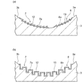
例如,如图9所示也可以将衍射光栅图形7a,8a直接(不设置衍射层5)形成于主体部3的凹部3a的曲面3b上。另外,衍射光栅图形7a,8a的种类如图9(a)所示也可以是锯齿状截面的闪耀光栅(blazedgrating),如图9(b)所示也可以是矩形状截面的二元衍射光栅(binarygrating)或者正弦波形状截面的全息光栅(holographic grating)。For example, as shown in FIG. 9 , the
另外,不将光通过孔4b设置于光检测元件4,作为使光Lm入射到凹部3a的光入射部,可以将光通过孔设置于作为光吸收层的基板2的区域R1或光吸收层27的区域R1。再有,由分光模块处理的衍射次数并不限于光L1为-1次光、光L2为0次光,光L1和光L2的次数也可以不同。In addition, instead of providing the
产业上的利用可能性Industrial Utilization Possibility
根据本发明,能够提供一种能够防止大型化并能够高精度地检测宽波长范围的光和不同波长范围的光的分光模块。According to the present invention, it is possible to provide a spectroscopic module capable of detecting light in a wide wavelength range and light in different wavelength ranges with high precision while preventing enlargement.
符号的说明Explanation of symbols
1…分光模块、2…基板、3…主体部、3a…凹部、3b…曲面、4…光检测元件(第1光检测元件)、4a…光检测部(第1光检测部)、4b…光通过孔、6…反射部、7…分光部(第1分光部)、8…分光部(第2分光部)、9…光检测元件(第2光检测元件)、9a…光检测部(第2光检测部)、R…区域(第1光检测部与第2光检测部之间的区域)、R1…区域(第1光检测元件与第2光检测元件之间的区域)、Lm…被测定光、L1…光(第1光)、L2…光(第2光)、L3…光(第3光)。1...spectroscopic module, 2...substrate, 3...main body, 3a...recess, 3b...curved surface, 4...photodetector (first photodetector), 4a...photodetector (first photodetector), 4b... Light passing hole, 6...reflecting part, 7...spectroscopic part (first spectroscopic part), 8...spectral part (second spectroscopic part), 9...photodetecting element (second photodetecting element), 9a...photodetecting part ( 2nd light detection part), R... area (the area between the 1st light detection part and the 2nd light detection part), R1... area (the area between the 1st light detection element and the 2nd light detection element), Lm ...light to be measured, L1...light (first light), L2...light (second light), L3...light (third light).
Claims (3)
Applications Claiming Priority (3)
| Application Number | Priority Date | Filing Date | Title |
|---|---|---|---|
| JP2010085204A JP5335729B2 (en) | 2010-04-01 | 2010-04-01 | Spectroscopic module |
| JP2010-085204 | 2010-04-01 | ||
| PCT/JP2011/056286 WO2011125443A1 (en) | 2010-04-01 | 2011-03-16 | Spectrometer module |
Publications (2)
| Publication Number | Publication Date |
|---|---|
| CN102822647A true CN102822647A (en) | 2012-12-12 |
| CN102822647B CN102822647B (en) | 2015-04-08 |
Family
ID=44762403
Family Applications (1)
| Application Number | Title | Priority Date | Filing Date |
|---|---|---|---|
| CN201180016763.XA Active CN102822647B (en) | 2010-04-01 | 2011-03-16 | Spectrometer module |
Country Status (5)
| Country | Link |
|---|---|
| US (2) | US9285270B2 (en) |
| JP (1) | JP5335729B2 (en) |
| CN (1) | CN102822647B (en) |
| DE (1) | DE112011101148B4 (en) |
| WO (1) | WO2011125443A1 (en) |
Cited By (4)
| Publication number | Priority date | Publication date | Assignee | Title |
|---|---|---|---|---|
| CN107850489A (en) * | 2015-08-04 | 2018-03-27 | 浜松光子学株式会社 | The manufacture method of optical splitter and optical splitter |
| CN109085701A (en) * | 2018-07-26 | 2018-12-25 | 京东方科技集团股份有限公司 | Beam splitting system and manufacturing method and spectrum detection instrument and manufacturing method comprising it |
| CN110440917A (en) * | 2014-02-05 | 2019-11-12 | 浜松光子学株式会社 | The manufacturing method of optical splitter and optical splitter |
| US11344884B2 (en) | 2018-07-26 | 2022-05-31 | Boe Technology Group Co., Ltd. | Microfluidic apparatus, method of detecting substance in microfluidic apparatus, and spectrometer |
Families Citing this family (21)
| Publication number | Priority date | Publication date | Assignee | Title |
|---|---|---|---|---|
| JP5415060B2 (en) | 2008-05-15 | 2014-02-12 | 浜松ホトニクス株式会社 | Spectroscopic module |
| JP5205239B2 (en) * | 2008-05-15 | 2013-06-05 | 浜松ホトニクス株式会社 | Spectrometer |
| JP5205242B2 (en) * | 2008-05-15 | 2013-06-05 | 浜松ホトニクス株式会社 | Spectrometer manufacturing method |
| JP2009300417A (en) * | 2008-05-15 | 2009-12-24 | Hamamatsu Photonics Kk | Spectroscopic module and its manufacturing method |
| JP5207938B2 (en) | 2008-05-15 | 2013-06-12 | 浜松ホトニクス株式会社 | Spectroscopic module and method for manufacturing spectral module |
| JP5205241B2 (en) * | 2008-05-15 | 2013-06-05 | 浜松ホトニクス株式会社 | Spectroscopic module |
| JP2009300422A (en) * | 2008-05-15 | 2009-12-24 | Hamamatsu Photonics Kk | Spectroscopic module |
| JP6234667B2 (en) * | 2012-08-06 | 2017-11-22 | 浜松ホトニクス株式会社 | Optical element and manufacturing method thereof |
| EP2857810A1 (en) * | 2013-10-02 | 2015-04-08 | Nederlandse Organisatie voor toegepast -natuurwetenschappelijk onderzoek TNO | Monolith spectrometer |
| JP6251073B2 (en) * | 2014-02-05 | 2017-12-20 | 浜松ホトニクス株式会社 | Spectrometer and method of manufacturing the spectrometer |
| JP6177153B2 (en) * | 2014-02-05 | 2017-08-09 | 浜松ホトニクス株式会社 | Spectrometer |
| JP6188743B2 (en) | 2014-06-19 | 2017-08-30 | キヤノン株式会社 | Optical element having a plurality of optical functional surfaces, spectroscopic device, and manufacturing method thereof |
| TWI627449B (en) * | 2016-04-15 | 2018-06-21 | 中央研究院 | Surface diffraction grating, spectrometer and curved diffraction grating manufacturing method |
| JP6383126B1 (en) * | 2018-04-17 | 2018-08-29 | 浜松ホトニクス株式会社 | Spectrometer |
| KR102806625B1 (en) * | 2018-07-06 | 2025-05-13 | 하마마츠 포토닉스 가부시키가이샤 | Spectroscopic module, and method for manufacturing spectroscopic module |
| JP6411693B1 (en) * | 2018-08-02 | 2018-10-24 | 浜松ホトニクス株式会社 | Spectrometer |
| JP2019002941A (en) * | 2018-09-26 | 2019-01-10 | 浜松ホトニクス株式会社 | Spectrometer |
| US11639873B2 (en) * | 2020-04-15 | 2023-05-02 | Viavi Solutions Inc. | High resolution multi-pass optical spectrum analyzer |
| JP2022096461A (en) * | 2020-12-17 | 2022-06-29 | キヤノン株式会社 | Optical system and surface spectroscopic apparatus |
| US12025494B2 (en) * | 2021-06-24 | 2024-07-02 | Corning Incorporated | Optical elements including hard oxide bodies and grating layers and method for making the same |
| US12571961B2 (en) * | 2022-06-08 | 2026-03-10 | Rockley Photonics Limited | Echelle gratings with a shared free propagation region |
Citations (7)
| Publication number | Priority date | Publication date | Assignee | Title |
|---|---|---|---|---|
| US4571074A (en) * | 1982-01-04 | 1986-02-18 | Instruments S.A. | Spectrometry device for analyzing polychromatic light |
| JP2000171300A (en) * | 1998-11-21 | 2000-06-23 | Sai G Fuer Analytische Messgeraete Mbh | Double grating-simultaneous spectrometer with semiconductor line sensor or photomultiplier |
| DE10137428A1 (en) * | 2001-07-27 | 2003-02-20 | Karlsruhe Forschzent | Device for measuring a solar UV radiation spectrum is configured to allow fast and simultaneous measurement of a spectrum with, at the same time, sufficiently high suppression of scattered light and sufficient dynamic range |
| CN101014841A (en) * | 2004-06-09 | 2007-08-08 | 应用光学电子光学及光谱学开发研究所 | Echelle spectrometer with improved use of the detector by means of two spectrometer arrangements |
| JP2009092680A (en) * | 2007-10-03 | 2009-04-30 | Yokogawa Electric Corp | Diffraction grating and spectroscopic device using the same |
| JP2009300414A (en) * | 2008-05-15 | 2009-12-24 | Hamamatsu Photonics Kk | Spectrometer |
| JP2009300420A (en) * | 2008-05-15 | 2009-12-24 | Hamamatsu Photonics Kk | Spectroscope manufacturing method |
Family Cites Families (13)
| Publication number | Priority date | Publication date | Assignee | Title |
|---|---|---|---|---|
| JP2662816B2 (en) | 1989-07-07 | 1997-10-15 | 富士変速機株式会社 | Underground multi-story parking system |
| DE4038638A1 (en) | 1990-12-04 | 1992-06-11 | Zeiss Carl Fa | DIODE LINE SPECTROMETER |
| FR2689349B1 (en) | 1992-03-31 | 1994-05-06 | Alcatel Nv | WAVELENGTH MULTIPLEXER FOR INTEGRATED OPTICAL SYSTEM. |
| WO2003069291A1 (en) | 2002-02-14 | 2003-08-21 | Containerless Research, Inc. | Photopolarimeters and spectrophotopolarimaters with multiple diffraction gratings |
| US7733492B1 (en) * | 2004-06-04 | 2010-06-08 | University Of Hawaii | Sagnac fourier transform spectrometer having improved resolution |
| DE102006017705B4 (en) | 2006-04-15 | 2010-01-07 | Carl Zeiss Microimaging Gmbh | Spectral analysis unit with a diffraction grating and laser scanning microscope |
| US7697137B2 (en) * | 2006-04-28 | 2010-04-13 | Corning Incorporated | Monolithic Offner spectrometer |
| DE102007027008A1 (en) * | 2007-06-08 | 2008-12-11 | Spectro Analytical Instruments Gmbh & Co. Kg | Spectrometers with solid state sensors and secondary electron multipliers |
| EP2063239A4 (en) * | 2007-06-08 | 2013-12-25 | Hamamatsu Photonics Kk | Spectroscopic module |
| CN100545697C (en) | 2007-12-29 | 2009-09-30 | 苏州大学 | Minisized hyper-spectral image-forming system |
| JP5207938B2 (en) | 2008-05-15 | 2013-06-12 | 浜松ホトニクス株式会社 | Spectroscopic module and method for manufacturing spectral module |
| JP2009300418A (en) * | 2008-05-15 | 2009-12-24 | Hamamatsu Photonics Kk | Spectroscopic module |
| JP5286955B2 (en) * | 2008-06-12 | 2013-09-11 | 株式会社Ihi | Foil bearing |
-
2010
- 2010-04-01 JP JP2010085204A patent/JP5335729B2/en active Active
-
2011
- 2011-03-16 WO PCT/JP2011/056286 patent/WO2011125443A1/en not_active Ceased
- 2011-03-16 DE DE112011101148.2T patent/DE112011101148B4/en active Active
- 2011-03-16 CN CN201180016763.XA patent/CN102822647B/en active Active
- 2011-03-16 US US13/637,410 patent/US9285270B2/en active Active
-
2016
- 2016-02-12 US US15/042,356 patent/US9851247B2/en active Active
Patent Citations (8)
| Publication number | Priority date | Publication date | Assignee | Title |
|---|---|---|---|---|
| US4571074A (en) * | 1982-01-04 | 1986-02-18 | Instruments S.A. | Spectrometry device for analyzing polychromatic light |
| JPH0339572B2 (en) * | 1982-01-04 | 1991-06-14 | Instruments Sa | |
| JP2000171300A (en) * | 1998-11-21 | 2000-06-23 | Sai G Fuer Analytische Messgeraete Mbh | Double grating-simultaneous spectrometer with semiconductor line sensor or photomultiplier |
| DE10137428A1 (en) * | 2001-07-27 | 2003-02-20 | Karlsruhe Forschzent | Device for measuring a solar UV radiation spectrum is configured to allow fast and simultaneous measurement of a spectrum with, at the same time, sufficiently high suppression of scattered light and sufficient dynamic range |
| CN101014841A (en) * | 2004-06-09 | 2007-08-08 | 应用光学电子光学及光谱学开发研究所 | Echelle spectrometer with improved use of the detector by means of two spectrometer arrangements |
| JP2009092680A (en) * | 2007-10-03 | 2009-04-30 | Yokogawa Electric Corp | Diffraction grating and spectroscopic device using the same |
| JP2009300414A (en) * | 2008-05-15 | 2009-12-24 | Hamamatsu Photonics Kk | Spectrometer |
| JP2009300420A (en) * | 2008-05-15 | 2009-12-24 | Hamamatsu Photonics Kk | Spectroscope manufacturing method |
Cited By (6)
| Publication number | Priority date | Publication date | Assignee | Title |
|---|---|---|---|---|
| CN110440917A (en) * | 2014-02-05 | 2019-11-12 | 浜松光子学株式会社 | The manufacturing method of optical splitter and optical splitter |
| CN107850489A (en) * | 2015-08-04 | 2018-03-27 | 浜松光子学株式会社 | The manufacture method of optical splitter and optical splitter |
| US10408677B2 (en) | 2015-08-04 | 2019-09-10 | Hamamatsu Photonics K.K. | Spectroscope, and spectroscope production method |
| CN107850489B (en) * | 2015-08-04 | 2019-12-20 | 浜松光子学株式会社 | Optical splitter and method for manufacturing optical splitter |
| CN109085701A (en) * | 2018-07-26 | 2018-12-25 | 京东方科技集团股份有限公司 | Beam splitting system and manufacturing method and spectrum detection instrument and manufacturing method comprising it |
| US11344884B2 (en) | 2018-07-26 | 2022-05-31 | Boe Technology Group Co., Ltd. | Microfluidic apparatus, method of detecting substance in microfluidic apparatus, and spectrometer |
Also Published As
| Publication number | Publication date |
|---|---|
| DE112011101148T5 (en) | 2013-01-10 |
| JP2011215074A (en) | 2011-10-27 |
| DE112011101148B4 (en) | 2021-12-30 |
| JP5335729B2 (en) | 2013-11-06 |
| US9285270B2 (en) | 2016-03-15 |
| WO2011125443A1 (en) | 2011-10-13 |
| US9851247B2 (en) | 2017-12-26 |
| US20160161334A1 (en) | 2016-06-09 |
| CN102822647B (en) | 2015-04-08 |
| US20130038874A1 (en) | 2013-02-14 |
Similar Documents
| Publication | Publication Date | Title |
|---|---|---|
| CN102822647B (en) | Spectrometer module | |
| CN102834702B (en) | Optical module | |
| CN101970995B (en) | Method for manufacturing spectrometer | |
| KR101563009B1 (en) | spectroscope | |
| JP4887221B2 (en) | Spectroscopic module | |
| KR101518518B1 (en) | Spectroscopic module | |
| JP5512961B2 (en) | Spectroscopic module and manufacturing method thereof | |
| KR101735131B1 (en) | Spectroscopy module and manufacturing method therefor | |
| JP5205240B2 (en) | Spectroscopic module manufacturing method and spectroscopic module | |
| CN101542246A (en) | Light splitting module | |
| CN101970994A (en) | Splitter | |
| WO2009139315A1 (en) | Spectral module | |
| JP4887251B2 (en) | Spectroscopic module | |
| JP4887250B2 (en) | Spectroscopic module | |
| WO2009139320A1 (en) | Spectral module | |
| KR20110005773A (en) | Manufacturing Method and Spectroscopy Module | |
| JP5113947B2 (en) | Spectroscopic module | |
| JP4980184B2 (en) | Spectroscopic module | |
| JP5097294B2 (en) | Spectroscopic module | |
| JP5825880B2 (en) | Spectroscopic module |
Legal Events
| Date | Code | Title | Description |
|---|---|---|---|
| C06 | Publication | ||
| PB01 | Publication | ||
| C10 | Entry into substantive examination | ||
| SE01 | Entry into force of request for substantive examination | ||
| C14 | Grant of patent or utility model | ||
| GR01 | Patent grant |