CN102543679A - Method for cleaning a semiconductor wafer composed of silicon directly after a process of polishing of the semiconductor wafer - Google Patents
Method for cleaning a semiconductor wafer composed of silicon directly after a process of polishing of the semiconductor wafer Download PDFInfo
- Publication number
- CN102543679A CN102543679A CN2011104379456A CN201110437945A CN102543679A CN 102543679 A CN102543679 A CN 102543679A CN 2011104379456 A CN2011104379456 A CN 2011104379456A CN 201110437945 A CN201110437945 A CN 201110437945A CN 102543679 A CN102543679 A CN 102543679A
- Authority
- CN
- China
- Prior art keywords
- semiconductor wafer
- seconds
- cleaning
- water
- duration
- Prior art date
- Legal status (The legal status is an assumption and is not a legal conclusion. Google has not performed a legal analysis and makes no representation as to the accuracy of the status listed.)
- Granted
Links
Images


Classifications
-
- H—ELECTRICITY
- H10—SEMICONDUCTOR DEVICES; ELECTRIC SOLID-STATE DEVICES NOT OTHERWISE PROVIDED FOR
- H10P—GENERIC PROCESSES OR APPARATUS FOR THE MANUFACTURE OR TREATMENT OF DEVICES COVERED BY CLASS H10
- H10P50/00—Etching of wafers, substrates or parts of devices
-
- H—ELECTRICITY
- H10—SEMICONDUCTOR DEVICES; ELECTRIC SOLID-STATE DEVICES NOT OTHERWISE PROVIDED FOR
- H10P—GENERIC PROCESSES OR APPARATUS FOR THE MANUFACTURE OR TREATMENT OF DEVICES COVERED BY CLASS H10
- H10P70/00—Cleaning of wafers, substrates or parts of devices
- H10P70/10—Cleaning before device manufacture, i.e. Begin-Of-Line process
- H10P70/15—Cleaning before device manufacture, i.e. Begin-Of-Line process by wet cleaning only
-
- H—ELECTRICITY
- H10—SEMICONDUCTOR DEVICES; ELECTRIC SOLID-STATE DEVICES NOT OTHERWISE PROVIDED FOR
- H10P—GENERIC PROCESSES OR APPARATUS FOR THE MANUFACTURE OR TREATMENT OF DEVICES COVERED BY CLASS H10
- H10P90/00—Preparation of wafers not covered by a single main group of this subclass, e.g. wafer reinforcement
- H10P90/12—Preparing bulk and homogeneous wafers
- H10P90/129—Preparing bulk and homogeneous wafers by polishing
Landscapes
- Cleaning Or Drying Semiconductors (AREA)
- Mechanical Treatment Of Semiconductor (AREA)
Abstract
在化学机械抛光由硅组成的半导体晶片之后立即清洁该半导体晶片的方法,该方法包括以所示顺序进行的以下步骤:a)将半导体晶片从抛光盘转移至第一清洁模块,其中在转移过程中用水以不大于1000Pa的压力喷射半导体晶片的两个侧面至少一次;b)在导入水的情况下在旋转的滚筒之间清洁半导体晶片;c)用含有氟化氢和表面活性剂的水溶液以不大于70000Pa的压力喷射半导体晶片的侧面;d)用水以不大于20000Pa的压力喷射半导体晶片的侧面;e)将半导体晶片浸入含水的碱性清洁溶液中;f)在导入水的情况下在旋转的滚筒之间清洁半导体晶片;g)用水喷射半导体晶片;及h)干燥半导体晶片。
A method of cleaning a semiconductor wafer consisting of silicon immediately after chemical mechanical polishing of the semiconductor wafer, the method comprising the following steps in the order shown: a) transferring the semiconductor wafer from the polishing disc to a first cleaning module, wherein during the transfer Spraying the two sides of the semiconductor wafer with water at a pressure not greater than 1000Pa at least once; b) cleaning the semiconductor wafer between rotating drums while introducing water; c) using an aqueous solution containing hydrogen fluoride and a surfactant at a pressure not greater than Spraying the side of the semiconductor wafer with a pressure of 70000Pa; d) spraying the side of the semiconductor wafer with water at a pressure not greater than 20000Pa; e) immersing the semiconductor wafer in an aqueous alkaline cleaning solution; f) rotating the drum while introducing water between cleaning the semiconductor wafer; g) spraying the semiconductor wafer with water; and h) drying the semiconductor wafer.
Description
技术领域 technical field
本发明涉及在化学机械抛光由硅组成的半导体晶片之后立即对该半导体晶片清洁去除抛光剂残余物的方法。The present invention relates to a method for cleaning a semiconductor wafer composed of silicon from polishing agent residues immediately after chemical mechanical polishing of the semiconductor wafer.
背景技术 Background technique
通常对由硅组成的半导体晶片实施化学机械抛光(CMP)以使半导体晶片的一个或两个面光滑化。在抛光之后,半导体晶片被抛光剂的残余物污染,并且必须加以清洁。必须尽可能迅速地去除该残余物,这是因为其会进攻半导体晶片的敏感表面,并且必需尽可能完全地加以去除,这是因为留在经清洁的表面上的颗粒会导致表面缺陷,之后这些表面缺陷无法通过清洁加以去除。此外,出于经济方面的原因,该清洁过程还必须在尽可能短的时间内完成。Chemical mechanical polishing (CMP) is commonly performed on semiconductor wafers composed of silicon to smooth one or both sides of the semiconductor wafer. After polishing, the semiconductor wafer is contaminated with residues of polishing agents and must be cleaned. This residue must be removed as quickly as possible, since it attacks the sensitive surface of the semiconductor wafer, and must be removed as completely as possible, since particles remaining on the cleaned surface can cause surface defects, which are then Surface defects cannot be removed by cleaning. Furthermore, for economical reasons, this cleaning process must also be carried out in the shortest possible time.
DE 102007032385A1描述了一种用于在CMP之后在模块结构化的清洁设备中清洁半导体晶片的方法。在该方法中,分别单独地在至少两个清洁模块中对半导体晶片进行清洁,并在一个干燥模块中进行干燥。目的在于去除金属污染物的包括三个子步骤的清洁序列在同一清洁模块中进行。DE 102007032385A1 describes a method for cleaning semiconductor wafers after CMP in a modular cleaning system. In this method, the semiconductor wafers are cleaned separately in at least two cleaning modules and dried in a drying module. A cleaning sequence comprising three sub-steps aimed at removing metal contaminants is carried out in the same cleaning module.
在EP 0708480A1中,作为用包含氢氧化铵、过氧化氢和水的清洁溶液进行清洁的有利的替代方案,建议半导体晶片在抛光之后首先用氢氟酸水溶液进行清洁,随后用包含臭氧的水进行冲洗,最后在存在水的情况下用刷子进行清洁。In EP 0708480A1, as an advantageous alternative to cleaning with a cleaning solution comprising ammonium hydroxide, hydrogen peroxide and water, it is proposed that after polishing semiconductor wafers are firstly cleaned with aqueous hydrofluoric acid and subsequently with water comprising ozone Rinse and finally clean with a brush in the presence of water.
US 5,944,906描述了一种方法,通过该方法在抛光之后对其表面由至少两种不同材料形成的半导体晶片进行清洁。在采用该方法时,半导体晶片彼此先后依次用一系列含水的清洁溶液进行处理。该系列包括氢氟酸、pH在1至4的范围内的表面活性剂溶液、氢氧化铵水溶液、pH在8至10的范围内的表面活性剂溶液和去离子水。US 5,944,906 describes a method by which after polishing a semiconductor wafer whose surface is formed from at least two different materials is cleaned. In this method, the semiconductor wafers are treated one behind the other with a series of aqueous cleaning solutions. The series includes hydrofluoric acid, surfactant solutions with a pH in the range of 1 to 4, aqueous ammonium hydroxide, surfactant solutions with a pH in the range of 8 to 10, and deionized water.
发明内容 Contents of the invention
本发明的目的在于,提供一种清洁方法,通过该方法可以对由硅组成的半导体晶片在化学机械抛光之后单独地及以高的通过量有效地去除在经抛光的正面和背面上的抛光残余物。It is an object of the present invention to provide a cleaning method by which polishing residues on the polished front side and rear side of a semiconductor wafer made of silicon can be removed efficiently individually and with a high throughput after chemical mechanical polishing things.
该目的是通过在化学机械抛光由硅组成的半导体晶片之后立即清洁该半导体晶片的方法实现的,该方法包括以所示顺序进行的以下步骤:This object is achieved by a method for cleaning a semiconductor wafer consisting of silicon immediately after chemical mechanical polishing of the semiconductor wafer, which method comprises the following steps in the order indicated:
a)将半导体晶片从抛光盘转移至第一清洁模块,其中在转移过程中用水以不大于1000Pa的压力喷射半导体晶片的两个侧面至少一次;a) transferring the semiconductor wafer from the polishing disc to the first cleaning module, wherein water is sprayed at least once on both sides of the semiconductor wafer at a pressure not greater than 1000 Pa during the transfer;
b)在导入水的情况下在旋转的滚筒之间清洁半导体晶片;b) cleaning of semiconductor wafers between rotating drums with the introduction of water;
c)用含有氟化氢和表面活性剂的水溶液以不大于70000Pa的压力喷射半导体晶片的侧面;c) Spraying the side of the semiconductor wafer with an aqueous solution containing hydrogen fluoride and a surfactant at a pressure not greater than 70000Pa;
d)用水以不大于20000Pa的压力喷射半导体晶片的侧面;d) Spray the side of the semiconductor wafer with water at a pressure not greater than 20000Pa;
e)将半导体晶片浸入含水的碱性清洁溶液中;e) immersing the semiconductor wafer in an aqueous alkaline cleaning solution;
f)在导入水的情况下在旋转的滚筒之间清洁半导体晶片;f) cleaning of semiconductor wafers between rotating drums with the introduction of water;
g)用水喷射半导体晶片;及g) spraying the semiconductor wafer with water; and
h)干燥半导体晶片。h) Drying the semiconductor wafer.
附图说明 Description of drawings
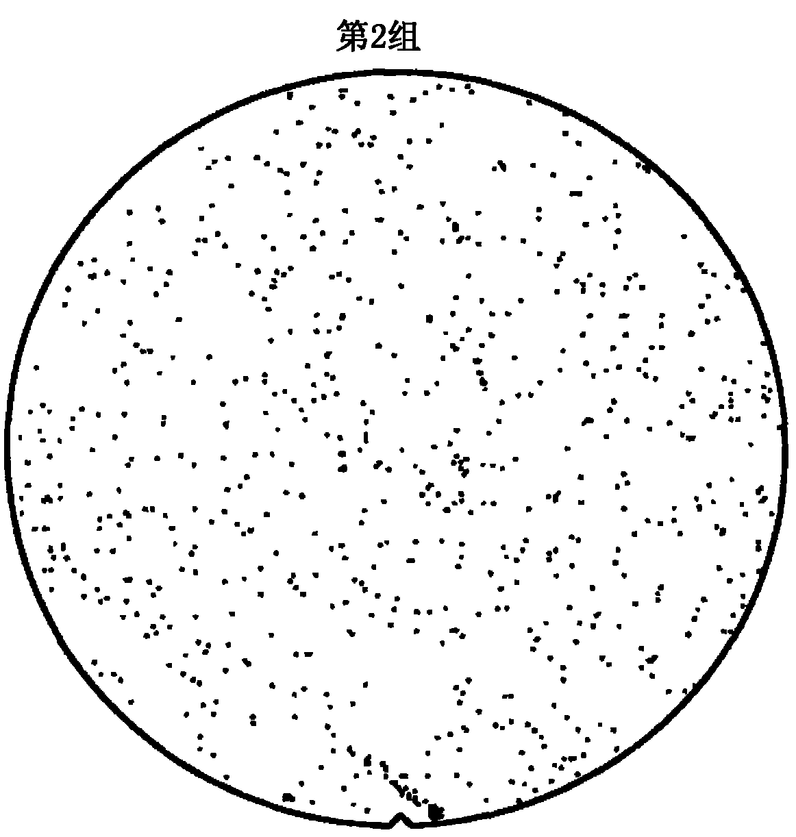
图1和2所示为在正面上发现的颗粒的分布图,其中每个图显示了在每组半导体晶片的经抛光的半导体晶片正面上发现的颗粒的总数。1 and 2 are graphs showing the distribution of particles found on the front side, where each graph shows the total number of particles found on the polished semiconductor wafer front side for each set of semiconductor wafers.
图3和4所示为在正面上发现的颗粒的分布图,其中每个图显示了在每组半导体晶片的半导体晶片正面上发现的颗粒的总数。3 and 4 are graphs showing the distribution of particles found on the front side, where each graph shows the total number of particles found on the front side of the semiconductor wafers for each set of semiconductor wafers.
具体实施方式 Detailed ways
该方法能够在化学机械抛光由硅组成的半导体晶片之后立即迅速且有效地清洁半导体晶片的经抛光的正面和背面。The method enables rapid and efficient cleaning of the polished front and back sides of the semiconductor wafer immediately after chemical mechanical polishing of the semiconductor wafer consisting of silicon.
半导体晶片在该方法中于不同的清洁模块中进行处理。清洁模块是功能单元,在其中半导体晶片的清洁是通过用液体喷射半导体晶片的侧面,通过将半导体晶片浸入浴中或者通过在导入水或导入清洁溶液的情况下在旋转的滚筒之间清洁半导体晶片而进行的。优选的是,在所述处理期间在清洁模块中半导体晶片绕其中心旋转,优选在垂直平面内旋转。Semiconductor wafers are processed in different cleaning modules in this method. The cleaning module is the functional unit in which the semiconductor wafers are cleaned by spraying the sides of the semiconductor wafers with liquid, by immersing the semiconductor wafers in a bath or by cleaning the semiconductor wafers between rotating drums with the introduction of water or the introduction of cleaning solutions And carried out. Preferably, the semiconductor wafer is rotated about its center, preferably in a vertical plane, in the cleaning module during said processing.
该方法包括特定的操作顺序,其在整体上实现了本发明的目的。根据该方法清洁的由硅组成的半导体晶片在被颗粒污染方面具有已经在将要进行包装及发送给客户的经抛光的由硅组成的半导体晶片所期待的范围内的清洁度。与此同时,从根据该方法的步骤a)由抛光盘进行转移计算至在该方法的步骤h)中的干燥完全结束,其中计入了半导体晶片由机器人进行输送的时间,该方法耗时不大于360秒,优选不大于300秒。The method comprises a specific sequence of operations which in its entirety achieves the object of the invention. Semiconductor wafers consisting of silicon cleaned according to the method have a degree of cleanliness with respect to particle contamination already in the range expected for polished semiconductor wafers consisting of silicon which are to be packaged and sent to customers. At the same time, the calculation from the transfer by the polishing disc according to step a) of the method to the complete end of the drying in step h) of the method takes into account the time during which the semiconductor wafer is transported by the robot, which takes less than 10 minutes. More than 360 seconds, preferably not more than 300 seconds.
在采用该方法时,每单位时间(循环时间)经干燥的半导体晶片的产出量为每75秒至少一个半导体晶片,优选为每66秒至少一个半导体晶片。When using this method, the throughput of dried semiconductor wafers per unit time (cycle time) is at least one semiconductor wafer per 75 seconds, preferably at least one semiconductor wafer per 66 seconds.
该方法包括从抛光盘转移至第一清洁模块、清洁步骤b)至g)以及最后在干燥模块中干燥半导体晶片。为了实施该方法的清洁步骤b)至g),优选使用不多于3个清洁模块,这有助于获得高的通过量。The method comprises transfer from the polishing pad to a first cleaning module, cleaning steps b) to g) and finally drying the semiconductor wafer in a drying module. For carrying out the cleaning steps b) to g) of the method, preferably no more than 3 cleaning modules are used, which contributes to a high throughput.
用于清洁半导体晶片的水优选为去离子水。The water used for cleaning semiconductor wafers is preferably deionized water.
在该方法开始时,将在其经抛光的正面及其背面粘附有抛光剂残余物的半导体晶片尽可能迅速地从抛光盘输送至第一清洁模块。在该转移过程中,用水喷射半导体晶片的两个面至少一次,其中半导体晶片优选保持水平或垂直。特别优选将半导体晶片借助于将其于边缘处进行夹持的机器人系统输送至接受站(
在该方法的步骤a)的过程中用水喷射半导体晶片的侧面所采用的压力为不大于1000Pa(10mbar)。若在该方法的此处的压力更高,则存在当用水喷射新鲜抛光且因此敏感的半导体晶片时由于更高的压力而产生无法在之后通过清洁加以去除的表面缺陷的风险。The pressure used to spray the side of the semiconductor wafer with water during step a) of the method is not greater than 1000 Pa (10 mbar). If the pressure is higher at this point in the method, there is a risk that when the freshly polished and thus sensitive semiconductor wafer is sprayed with water, surface defects which cannot be subsequently removed by cleaning are produced due to the higher pressure.
该方法的步骤b)至d)优选在第一清洁模块中实施。Steps b) to d) of the method are preferably carried out in the first cleaning module.
该方法的步骤b)包括在导入水的情况下在旋转的滚筒之间清洁半导体晶片。该滚筒优选具有由诸如聚乙烯醇的塑料制成的海绵状覆盖物,其在清洁时与半导体晶片接触。旋转的刷子也是合适的。半导体晶片在该处理过程中优选保持垂直,并绕其中心旋转。该方法的步骤b)耗时优选不小于10秒且不大于30秒。若时间短于10秒,则对该方法的效果有不利影响,而若长于30秒,则不利于该方法的生产率。Step b) of the method consists in cleaning the semiconductor wafer between rotating drums under the introduction of water. The roller preferably has a spongy covering made of plastic, such as polyvinyl alcohol, which comes into contact with the semiconductor wafer during cleaning. Rotating brushes are also suitable. The semiconductor wafer is preferably held vertically and rotated about its center during this process. Step b) of the method preferably takes no less than 10 seconds and no more than 30 seconds. If the time is shorter than 10 seconds, the effect of the method is adversely affected, and if it is longer than 30 seconds, the productivity of the method is disadvantageous.
该方法的步骤c)包括用含有氟化氢和至少一种表面活性剂的水溶液喷射半导体晶片的侧面。半导体晶片在该处理过程中优选保持垂直,并绕其中心旋转。该方法的步骤c)耗时优选不小于20秒且不大于30秒。若时间短于20秒,则对该方法的效果有不利影响,而若长于30秒,则不利于该方法的生产率。Step c) of the method comprises spraying the side of the semiconductor wafer with an aqueous solution comprising hydrogen fluoride and at least one surfactant. The semiconductor wafer is preferably held vertically and rotated about its center during this process. Step c) of the method preferably takes no less than 20 seconds and no more than 30 seconds. If the time is shorter than 20 seconds, the effect of the method is adversely affected, and if it is longer than 30 seconds, the productivity of the method is adversely affected.
氟化氢(HF)的浓度优选为0.5至1.5重量%,表面活性剂的浓度优选为0.015至0.03重量%。优选考虑包含一个或多个酸基且相应地形成pH小于7的水溶液的表面活性剂。The concentration of hydrogen fluoride (HF) is preferably 0.5 to 1.5% by weight, and the concentration of the surfactant is preferably 0.015 to 0.03% by weight. Preference is given to surfactants which contain one or more acid groups and accordingly form aqueous solutions with a pH of less than 7.
在该方法的步骤c)的过程中用水溶液喷射半导体晶片的侧面所采用的压力为不大于70000Pa(0.7bar)且优选不小于40000Pa(0.4bar)。若在该方法的此处的压力更高,则存在当用水溶液喷射半导体晶片时产生无法在之后通过清洁加以去除的表面缺陷的风险。若压力过低,则清洁不完全。The pressure employed to spray the side of the semiconductor wafer with the aqueous solution during step c) of the method is not more than 70000 Pa (0.7 bar) and preferably not less than 40000 Pa (0.4 bar). If the pressure is higher at this point of the method, there is a risk that when the semiconductor wafer is sprayed with an aqueous solution, surface defects will be produced which cannot be subsequently removed by cleaning. If the pressure is too low, cleaning will not be complete.
该方法的步骤d)包括用水喷射半导体晶片的侧面。半导体晶片在该处理过程中优选保持垂直,并绕其中心旋转。该方法的步骤d)耗时优选不小于1秒且不大于10秒。若时间长于10秒,则不利于该方法的生产率。Step d) of the method comprises spraying the sides of the semiconductor wafer with water. The semiconductor wafer is preferably held vertically and rotated about its center during this process. Step d) of the method preferably takes no less than 1 second and no more than 10 seconds. A time longer than 10 seconds is detrimental to the productivity of the process.
在步骤d)的过程中用水喷射半导体晶片的侧面所采用的压力为不大于20000Pa(0.2bar)。若在该方法的此处的压力更高,则存在当用水喷射半导体晶片时产生无法在之后通过清洁加以去除的表面缺陷的风险。The pressure used to spray the side of the semiconductor wafer with water during step d) is not greater than 20000 Pa (0.2 bar). If the pressure is higher here in the method, there is a risk that when the semiconductor wafer is sprayed with water, surface defects are produced which cannot be subsequently removed by cleaning.
该方法的步骤e)优选在第二清洁模块中实施。包括将半导体晶片浸入含水的碱性清洁溶液中。半导体晶片在该处理过程中优选保持垂直,并绕其中心旋转。该清洁溶液的温度优选为不小于50℃且不大于60℃。其包含碱性化合物,优选为氢氧化四甲基铵(TMAH),以及任选存在的过氧化氢(H2O2)。碱性化合物的浓度优选在0.1至0.4重量%的范围内,过氧化氢的浓度优选在0.7至1.5重量%的范围内。Step e) of the method is preferably carried out in a second cleaning module. Involves immersing semiconductor wafers in an aqueous alkaline cleaning solution. The semiconductor wafer is preferably held vertically and rotated about its center during this process. The temperature of the cleaning solution is preferably not less than 50°C and not more than 60°C. It comprises a basic compound, preferably tetramethylammonium hydroxide (TMAH), and optionally hydrogen peroxide (H 2 O 2 ). The concentration of the basic compound is preferably in the range of 0.1 to 0.4% by weight, and the concentration of hydrogen peroxide is preferably in the range of 0.7 to 1.5% by weight.
该方法的步骤e)耗时优选不小于40秒且不大于60秒。若时间短于40秒,则对该方法的效果有不利影响,而若长于60秒,则不利于该方法的生产率。Step e) of the method preferably takes no less than 40 seconds and no more than 60 seconds. If the time is shorter than 40 seconds, the effect of the method is adversely affected, and if it is longer than 60 seconds, the productivity of the method is disadvantageous.
该方法的步骤f)和g)优选在第三清洁模块中实施。Steps f) and g) of the method are preferably carried out in a third cleaning module.
该方法的步骤f)包括在导入水的情况下在旋转的滚筒之间清洁半导体晶片。该滚筒优选具有由诸如聚乙烯醇的塑料制成的海绵状覆盖物,其在清洁时与半导体晶片接触。旋转的刷子同样是合适的。半导体晶片在该处理过程中优选保持垂直,并绕其中心旋转。该方法的步骤f)耗时优选不小于10秒且不大于30秒。若时间短于10秒,则对该方法的效果有不利影响,而若长于30秒,则不利于该方法的生产率。Step f) of the method consists in cleaning the semiconductor wafer between rotating drums with the introduction of water. The roller preferably has a spongy covering made of plastic, such as polyvinyl alcohol, which comes into contact with the semiconductor wafer during cleaning. Rotating brushes are likewise suitable. The semiconductor wafer is preferably held vertically and rotated about its center during this process. Step f) of the method preferably takes no less than 10 seconds and no more than 30 seconds. If the time is shorter than 10 seconds, the effect of the method is adversely affected, and if it is longer than 30 seconds, the productivity of the method is disadvantageous.
该方法的步骤g)包括用水喷射半导体晶片的侧面。半导体晶片在该处理过程中优选保持垂直,并绕其中心旋转。步骤g)耗时优选不小于5秒且不大于10秒。若时间短于5秒,则对该方法的效果有不利影响,而若长于10秒,则不利于该方法的生产率。Step g) of the method comprises spraying the sides of the semiconductor wafer with water. The semiconductor wafer is preferably held vertically and rotated about its center during this process. Step g) preferably takes no less than 5 seconds and no more than 10 seconds. If the time is shorter than 5 seconds, the effect of the method is adversely affected, and if it is longer than 10 seconds, the productivity of the method is disadvantageous.
该方法的步骤h)包括在干燥模块中干燥半导体晶片。特别优选为其中在存在异丙醇蒸汽的情况下进行干燥的干燥模块。干燥过程耗时优选不小于45秒且不大于65秒。Step h) of the method comprises drying the semiconductor wafer in a drying module. Particular preference is given to drying modules in which drying takes place in the presence of isopropanol vapors. The drying process preferably takes no less than 45 seconds and no more than 65 seconds.
根据本发明的方法适合于清洁由硅组成的半导体晶片,尤其是直径在200至450mm的范围内的由硅组成的半导体晶片。The method according to the invention is suitable for cleaning semiconductor wafers composed of silicon, in particular semiconductor wafers composed of silicon with a diameter in the range of 200 to 450 mm.
实施例1:Example 1:
对由硅组成的半导体晶片实施化学机械抛光,并以根据本发明的方式在抛光之后进行清洁。该方法的效果表现在进行包装及发送给客户之前在半导体晶片上测得的颗粒数量。对于一半数量的所检验的半导体晶片,发现不多于5个最大线性尺寸大于37nm的颗粒。还以比较的方式根据标准方法清洁半导体晶片。对于这些半导体晶片,对应的颗粒数量在15至20的范围内。A semiconductor wafer consisting of silicon is chemically mechanically polished and, in the manner according to the invention, cleaned after polishing. The effectiveness of this method is shown in the number of particles measured on semiconductor wafers before they are packaged and shipped to customers. For half the number of semiconductor wafers examined, no more than 5 particles were found with a largest linear dimension greater than 37 nm. Semiconductor wafers were also cleaned according to standard methods in a comparative manner. For these semiconductor wafers, the corresponding number of particles is in the range of 15 to 20.
实施例2:Example 2:
为了显示在步骤c)中表面活性剂的重要性,对第一组和第二组半导体晶片进行化学机械抛光和清洁。每组包括40个由硅组成的半导体晶片。根据本发明,第二组的清洁在抛光之后立即进行。第一组的清洁与此的区别仅在于在步骤c)中省略掉表面活性剂。对经清洁的半导体晶片实施根据现有技术的最终清洁,并检验尺寸为40nm或更大的颗粒的存在性。图1和2所示为在正面上发现的颗粒的分布图,其中每个图显示了在每组半导体晶片的经抛光的半导体晶片正面上发现的颗粒的总数。图1与图2的比较表明,在根据本发明清洁的半导体晶片(第二组,图2)的正面上发现的颗粒的数量明显低于在以非本发明方式进行清洁的半导体晶片(第一组,图1)的情况下所发现的颗粒数量。To show the importance of surfactants in step c), chemical mechanical polishing and cleaning were performed on the first and second set of semiconductor wafers. Each set consisted of 40 semiconductor wafers composed of silicon. According to the invention, the cleaning of the second group is carried out immediately after polishing. The cleaning of the first group differs from this only in that the surfactant is omitted in step c). The cleaned semiconductor wafers are subjected to a final cleaning according to the prior art and checked for the presence of particles with a size of 40 nm or more. 1 and 2 are graphs showing the distribution of particles found on the front side, where each graph shows the total number of particles found on the polished semiconductor wafer front side for each set of semiconductor wafers. A comparison of Fig. 1 with Fig. 2 shows that the number of particles found on the front side of semiconductor wafers cleaned according to the invention (second group, Fig. 2) is significantly lower than that of semiconductor wafers cleaned in a manner not according to the invention (first group) group, the number of particles found in the case of Figure 1).
实施例3:Example 3:
为了显示在步骤c)中压力的重要性,对第三组和第四组半导体晶片进行化学机械抛光和清洁。每组包括10个由硅组成的半导体晶片。根据本发明,第四组的清洁在抛光之后立即进行。第三组的清洁与此的区别仅在于在步骤c)中用水溶液以100000Pa的压力喷射半导体晶片的侧面。为了清洁第四组的半导体晶片,设置60000Pa的相应的压力。对经清洁的半导体晶片实施根据现有技术的最终清洁,并检验尺寸为40nm或更大的颗粒的存在性。图3和4所示为在正面上发现的颗粒的分布图,其中每个图显示了在每组半导体晶片的半导体晶片正面上发现的颗粒的总数。图3与图4的比较表明,在根据本发明清洁的半导体晶片(第四组,图4)的正面上发现的颗粒的数量明显低于在以非本发明方式进行清洁的半导体晶片(第三组,图3)的情况下所发现的颗粒数量。To show the importance of pressure in step c), the third and fourth sets of semiconductor wafers were chemically mechanically polished and cleaned. Each set consisted of 10 semiconductor wafers composed of silicon. According to the invention, cleaning of the fourth group is carried out immediately after polishing. The cleaning of the third group differs from this only in that in step c) the sides of the semiconductor wafer are sprayed with an aqueous solution at a pressure of 100,000 Pa. For cleaning the semiconductor wafers of the fourth group, a corresponding pressure of 60,000 Pa was set. The cleaned semiconductor wafers are subjected to a final cleaning according to the prior art and checked for the presence of particles with a size of 40 nm or more. 3 and 4 are graphs showing the distribution of particles found on the front side, where each graph shows the total number of particles found on the front side of the semiconductor wafers for each set of semiconductor wafers. A comparison of Fig. 3 with Fig. 4 shows that the number of particles found on the front side of semiconductor wafers cleaned according to the invention (fourth group, Fig. 4) is significantly lower than that of semiconductor wafers cleaned in a manner not according to the invention (third group). group, Figure 3) in the case of the number of particles found.
Claims (7)
Applications Claiming Priority (2)
| Application Number | Priority Date | Filing Date | Title |
|---|---|---|---|
| DE102010063178.7 | 2010-12-15 | ||
| DE102010063178.7A DE102010063178B4 (en) | 2010-12-15 | 2010-12-15 | Method for cleaning a semiconductor wafer of silicon immediately after polishing the semiconductor wafer |
Publications (2)
| Publication Number | Publication Date |
|---|---|
| CN102543679A true CN102543679A (en) | 2012-07-04 |
| CN102543679B CN102543679B (en) | 2014-11-26 |
Family
ID=46232724
Family Applications (1)
| Application Number | Title | Priority Date | Filing Date |
|---|---|---|---|
| CN201110437945.6A Active CN102543679B (en) | 2010-12-15 | 2011-12-12 | Method for cleaning a semiconductor wafer composed of silicon directly after a process of polishing of the semiconductor wafer |
Country Status (8)
| Country | Link |
|---|---|
| US (1) | US8377219B2 (en) |
| JP (1) | JP5427876B2 (en) |
| KR (1) | KR101312784B1 (en) |
| CN (1) | CN102543679B (en) |
| DE (1) | DE102010063178B4 (en) |
| MY (1) | MY150799A (en) |
| SG (1) | SG182072A1 (en) |
| TW (1) | TWI438038B (en) |
Families Citing this family (2)
| Publication number | Priority date | Publication date | Assignee | Title |
|---|---|---|---|---|
| JP6602720B2 (en) * | 2016-04-04 | 2019-11-06 | グローバルウェーハズ・ジャパン株式会社 | Method for forming protective film on semiconductor substrate |
| US20240331999A1 (en) * | 2023-03-31 | 2024-10-03 | Applied Materials, Inc. | Systems and methods for nanohole wet cleans |
Citations (4)
| Publication number | Priority date | Publication date | Assignee | Title |
|---|---|---|---|---|
| US5656097A (en) * | 1993-10-20 | 1997-08-12 | Verteq, Inc. | Semiconductor wafer cleaning system |
| US5944906A (en) * | 1996-05-24 | 1999-08-31 | Micron Technology Inc | Wet cleans for composite surfaces |
| CN101211774A (en) * | 2006-12-29 | 2008-07-02 | 斯尔瑞恩公司 | Method for cleaning silicon wafers |
| CN101325152A (en) * | 2007-06-13 | 2008-12-17 | 硅电子股份公司 | Method for cleaning, drying and hydrophilizing semiconductor wafers |
Family Cites Families (19)
| Publication number | Priority date | Publication date | Assignee | Title |
|---|---|---|---|---|
| JP2543007B2 (en) * | 1993-08-23 | 1996-10-16 | 株式会社エンヤシステム | Wafer single wafer cleaning device |
| US5723019A (en) * | 1994-07-15 | 1998-03-03 | Ontrak Systems, Incorporated | Drip chemical delivery method and apparatus |
| JP3119289B2 (en) | 1994-10-21 | 2000-12-18 | 信越半導体株式会社 | Semiconductor wafer cleaning method |
| JPH11251275A (en) * | 1997-11-20 | 1999-09-17 | Canon Inc | Polishing apparatus, cleaning apparatus for polishing apparatus, polishing / cleaning method, and method for manufacturing wiring section |
| US5954888A (en) * | 1998-02-09 | 1999-09-21 | Speedfam Corporation | Post-CMP wet-HF cleaning station |
| JP3953682B2 (en) * | 1999-06-02 | 2007-08-08 | 株式会社荏原製作所 | Wafer cleaning equipment |
| JP2002299300A (en) | 2001-03-30 | 2002-10-11 | Kaijo Corp | Substrate treatment method |
| US20030045098A1 (en) * | 2001-08-31 | 2003-03-06 | Applied Materials, Inc. | Method and apparatus for processing a wafer |
| KR100811411B1 (en) | 2001-12-21 | 2008-03-07 | 주식회사 하이닉스반도체 | Chemical Mechanical Polishing Method of Semiconductor Devices |
| JP2004074021A (en) * | 2002-08-19 | 2004-03-11 | Dainippon Screen Mfg Co Ltd | Substrate processing unit and substrate cleaning unit |
| DE10394095D2 (en) | 2003-07-09 | 2006-11-02 | Rena Sondermaschinen Gmbh | Apparatus for cleaning wafers after the CMP process |
| US20050092348A1 (en) * | 2003-11-05 | 2005-05-05 | Ju-Chien Chiang | Method for cleaning an integrated circuit device using an aqueous cleaning composition |
| JP2005194585A (en) * | 2004-01-08 | 2005-07-21 | Ebara Corp | Method for treating substrate in wet process and apparatus for treating substrate |
| US20060272677A1 (en) * | 2004-07-01 | 2006-12-07 | Lee Nam P | Cleaning process for semiconductor substrates |
| US20080173335A1 (en) * | 2005-04-11 | 2008-07-24 | Doosan Mecatec Co., Ltd | Semiconductor Wafer Cleaning System |
| JP2007141926A (en) * | 2005-11-15 | 2007-06-07 | Sony Corp | Substrate processing apparatus and substrate processing method |
| DE102007032385B4 (en) | 2007-07-11 | 2010-04-01 | Siltronic Ag | Process for cleaning a semiconductor wafer to CMP |
| JP2009206141A (en) * | 2008-02-26 | 2009-09-10 | Fujitsu Microelectronics Ltd | Manufacturing method of semiconductor device |
| JP2010098237A (en) | 2008-10-20 | 2010-04-30 | Panasonic Corp | Method of manufacturing semiconductor device |
-
2010
- 2010-12-15 DE DE102010063178.7A patent/DE102010063178B4/en active Active
-
2011
- 2011-12-01 TW TW100144147A patent/TWI438038B/en active
- 2011-12-01 KR KR1020110127948A patent/KR101312784B1/en active Active
- 2011-12-06 US US13/311,577 patent/US8377219B2/en active Active
- 2011-12-07 SG SG2011090511A patent/SG182072A1/en unknown
- 2011-12-07 MY MYPI2011005941 patent/MY150799A/en unknown
- 2011-12-09 JP JP2011270158A patent/JP5427876B2/en active Active
- 2011-12-12 CN CN201110437945.6A patent/CN102543679B/en active Active
Patent Citations (4)
| Publication number | Priority date | Publication date | Assignee | Title |
|---|---|---|---|---|
| US5656097A (en) * | 1993-10-20 | 1997-08-12 | Verteq, Inc. | Semiconductor wafer cleaning system |
| US5944906A (en) * | 1996-05-24 | 1999-08-31 | Micron Technology Inc | Wet cleans for composite surfaces |
| CN101211774A (en) * | 2006-12-29 | 2008-07-02 | 斯尔瑞恩公司 | Method for cleaning silicon wafers |
| CN101325152A (en) * | 2007-06-13 | 2008-12-17 | 硅电子股份公司 | Method for cleaning, drying and hydrophilizing semiconductor wafers |
Also Published As
| Publication number | Publication date |
|---|---|
| US8377219B2 (en) | 2013-02-19 |
| US20120152278A1 (en) | 2012-06-21 |
| KR20120067284A (en) | 2012-06-25 |
| DE102010063178A1 (en) | 2012-06-21 |
| TW201236771A (en) | 2012-09-16 |
| CN102543679B (en) | 2014-11-26 |
| TWI438038B (en) | 2014-05-21 |
| JP5427876B2 (en) | 2014-02-26 |
| SG182072A1 (en) | 2012-07-30 |
| JP2012129525A (en) | 2012-07-05 |
| KR101312784B1 (en) | 2013-09-27 |
| DE102010063178B4 (en) | 2014-05-22 |
| MY150799A (en) | 2014-02-28 |
Similar Documents
| Publication | Publication Date | Title |
|---|---|---|
| JP3185753B2 (en) | Method for manufacturing semiconductor device | |
| JP2007165935A (en) | How to remove metal in scrubbers | |
| JP2009543344A (en) | Post-etch wafer surface cleaning with liquid meniscus | |
| CN109860085B (en) | Silicon wafer CMP post-processing equipment and processing technology | |
| CN101248514B (en) | Silicon surface preparation | |
| US9211568B2 (en) | Clean function for semiconductor wafer scrubber | |
| TW201325744A (en) | Method for treating pollutant of workpiece provided with yttrium oxide coating layer | |
| CN102543679B (en) | Method for cleaning a semiconductor wafer composed of silicon directly after a process of polishing of the semiconductor wafer | |
| JP7020507B2 (en) | Cleaning method for semiconductor wafers | |
| KR102109893B1 (en) | Bonded wafer manufacturing method | |
| JP5443819B2 (en) | Method for manufacturing a roughened substrate | |
| US12500077B2 (en) | Epitaxial wafer cleaning method | |
| JP2000049132A (en) | Method of cleaning semiconductor substrate | |
| KR20150068020A (en) | Method for Cleaning Wafer | |
| JP2000049133A (en) | Method of cleaning semiconductor substrate | |
| JP2024041501A (en) | Substrate processing method and substrate processing apparatus | |
| JP6405618B2 (en) | Silicon wafer manufacturing method | |
| JP2004140126A (en) | Method of drying semiconductor substrate after cleaning | |
| KR20070001745A (en) | Pretreatment Cleaning Method for Gate Oxide | |
| CN111199874A (en) | Silicon wafer cleaning process | |
| JP2002246349A (en) | Method and equipment for polishing and cleaning silicon wafer | |
| KR20070044967A (en) | Single wafer cleaning method | |
| KR20090044397A (en) | How to Clean Photomask | |
| JP2000235966A (en) | Method for cleaning silicon wafer storage container |
Legal Events
| Date | Code | Title | Description |
|---|---|---|---|
| C06 | Publication | ||
| PB01 | Publication | ||
| C10 | Entry into substantive examination | ||
| SE01 | Entry into force of request for substantive examination | ||
| C14 | Grant of patent or utility model | ||
| GR01 | Patent grant |