CN101819335B - Thermochromatic element and thermochromatic display device - Google Patents
Thermochromatic element and thermochromatic display device Download PDFInfo
- Publication number
- CN101819335B CN101819335B CN200910105810.2A CN200910105810A CN101819335B CN 101819335 B CN101819335 B CN 101819335B CN 200910105810 A CN200910105810 A CN 200910105810A CN 101819335 B CN101819335 B CN 101819335B
- Authority
- CN
- China
- Prior art keywords
- thermochromic
- heating arrangement
- thermochromatic
- carbon nano
- electrode
- Prior art date
- Legal status (The legal status is an assumption and is not a legal conclusion. Google has not performed a legal analysis and makes no representation as to the accuracy of the status listed.)
- Expired - Fee Related
Links
Images


Classifications
-
- G—PHYSICS
- G02—OPTICS
- G02F—OPTICAL DEVICES OR ARRANGEMENTS FOR THE CONTROL OF LIGHT BY MODIFICATION OF THE OPTICAL PROPERTIES OF THE MEDIA OF THE ELEMENTS INVOLVED THEREIN; NON-LINEAR OPTICS; FREQUENCY-CHANGING OF LIGHT; OPTICAL LOGIC ELEMENTS; OPTICAL ANALOGUE/DIGITAL CONVERTERS
- G02F1/00—Devices or arrangements for the control of the intensity, colour, phase, polarisation or direction of light arriving from an independent light source, e.g. switching, gating or modulating; Non-linear optics
- G02F1/01—Devices or arrangements for the control of the intensity, colour, phase, polarisation or direction of light arriving from an independent light source, e.g. switching, gating or modulating; Non-linear optics for the control of the intensity, phase, polarisation or colour
- G02F1/0147—Devices or arrangements for the control of the intensity, colour, phase, polarisation or direction of light arriving from an independent light source, e.g. switching, gating or modulating; Non-linear optics for the control of the intensity, phase, polarisation or colour based on thermo-optic effects
-
- G—PHYSICS
- G02—OPTICS
- G02F—OPTICAL DEVICES OR ARRANGEMENTS FOR THE CONTROL OF LIGHT BY MODIFICATION OF THE OPTICAL PROPERTIES OF THE MEDIA OF THE ELEMENTS INVOLVED THEREIN; NON-LINEAR OPTICS; FREQUENCY-CHANGING OF LIGHT; OPTICAL LOGIC ELEMENTS; OPTICAL ANALOGUE/DIGITAL CONVERTERS
- G02F2201/00—Constructional arrangements not provided for in groups G02F1/00 - G02F7/00
- G02F2201/12—Constructional arrangements not provided for in groups G02F1/00 - G02F7/00 electrode
-
- G—PHYSICS
- G02—OPTICS
- G02F—OPTICAL DEVICES OR ARRANGEMENTS FOR THE CONTROL OF LIGHT BY MODIFICATION OF THE OPTICAL PROPERTIES OF THE MEDIA OF THE ELEMENTS INVOLVED THEREIN; NON-LINEAR OPTICS; FREQUENCY-CHANGING OF LIGHT; OPTICAL LOGIC ELEMENTS; OPTICAL ANALOGUE/DIGITAL CONVERTERS
- G02F2202/00—Materials and properties
- G02F2202/36—Micro- or nanomaterials
Landscapes
- Physics & Mathematics (AREA)
- Nonlinear Science (AREA)
- General Physics & Mathematics (AREA)
- Optics & Photonics (AREA)
- Devices For Indicating Variable Information By Combining Individual Elements (AREA)
- Liquid Crystal (AREA)
- Electrochromic Elements, Electrophoresis, Or Variable Reflection Or Absorption Elements (AREA)
Abstract
Description
技术领域 technical field
本发明涉及一种热致变色元件及热致变色显示装置,尤其涉及一种应用碳纳米管的热致变色元件,以及使用该热致变色元件的热致变色显示装置。The invention relates to a thermochromic element and a thermochromic display device, in particular to a thermochromic element using carbon nanotubes and a thermochromic display device using the thermochromic element.
背景技术 Background technique
由于热致变色材料在不同的温度下可以显示不同的颜色,因此,可以应用于热致变色显示装置中作为具有显示功能的热致变色元件。现有的热致变色显示装置中的热致变色元件至少包括显色层与加热层,所述显色层与加热层贴合设置或间隔设置。其中,所述加热层主要由金属板组成。然而,金属板的热容及厚度较大,其作为加热层工作时,温度变化慢、电热转换效率低,从而使得热致变色元件工作时显色响应迟钝、能耗较大。此外,金属板的柔韧性能有限,其难以在柔性热致变色显示装置中作加热层。另外,现有的热致变色显示装置只能显示预定的图案,不能显示变化的图像。Since the thermochromic material can display different colors at different temperatures, it can be used in a thermochromic display device as a thermochromic element with a display function. A thermochromic element in an existing thermochromic display device at least includes a color-developing layer and a heating layer, and the color-developing layer and the heating layer are arranged in close contact or at intervals. Wherein, the heating layer is mainly composed of metal plates. However, the heat capacity and thickness of the metal plate are large. When it works as a heating layer, the temperature changes slowly and the electrothermal conversion efficiency is low, which makes the color response of the thermochromic element slow and consumes a lot of energy. In addition, the metal plate has limited flexibility, which makes it difficult to be used as a heating layer in a flexible thermochromic display device. In addition, the existing thermochromic display devices can only display predetermined patterns, but cannot display changing images.
为克服金属板作为热致变色元件的加热层的缺点,现有技术提供一种热致变色显示装置,该热致变色显示装置中的热致变色元件的加热层包括碳墨及一聚合物。其中,所述碳墨印刷在聚合物上。所述聚合物的材料为介电薄膜或聚酯薄膜。虽然,该热致变色元件可以应用于柔性热致变色显示装置中,但所述加热层的电阻会因环境的改变而改变;因此,该加热层不能为该热致变色元件提供一稳定的热源,从而造成该热致变色元件工作时显色不稳定,影响其显示效果。此外,由于碳墨印刷在聚合物上,聚合物的热容较大,使得该加热层的热容较大,其工作时,温度变化慢、电热转换效率低,从而使得热致变色元件工作时显色响应也较迟钝、能耗也较大。另外,该热致变色显示装置也只能显示预定的图案,不能显示变化的图像。In order to overcome the disadvantage of the metal plate being used as the heating layer of the thermochromic element, the prior art provides a thermochromic display device. The heating layer of the thermochromic element in the thermochromic display device includes carbon ink and a polymer. Wherein, the carbon ink is printed on the polymer. The polymer material is a dielectric film or a polyester film. Although the thermochromic element can be applied to a flexible thermochromic display device, the resistance of the heating layer will change due to changes in the environment; therefore, the heating layer cannot provide a stable heat source for the thermochromic element , resulting in unstable color rendering of the thermochromic element during operation, affecting its display effect. In addition, because the carbon ink is printed on the polymer, the heat capacity of the polymer is large, which makes the heat capacity of the heating layer large. When it works, the temperature changes slowly and the electrothermal conversion efficiency is low, so that the thermochromic element works The color response is also relatively slow, and the energy consumption is also relatively large. In addition, the thermochromic display device can only display predetermined patterns, but cannot display changing images.
为解决上述问题,Robert Parker等人于1993年4月13日公告的,公告号为US 5,202,677,标题为“使用热致变色材料的显示装置”的美国专利中揭示了一种热致变色显示装置20。请参阅图1,该热致变色显示装置20包括一基底21、一加热层40、一非热致变色显示层22以及热致变色显示层24、26、28,其中,所述非热致变色显示层22及热致变色显示层24、26、28设置于上述基底21的第一表面,且堆叠设置。所述加热层40设置于基底21的第二表面,该加热层40包括一对平行电极52、54及设置于该一对平行电极52、54之间的导电层50。该加热层40为一不锈钢沉积层。该热致变色显示装置20中的加热层40的电阻在使用过程中受环境的影响比较小,可以给热致变色显示层24、26、28提供稳定的热源。但,由于加热层40需要沉积于基底21上,该加热层40工作时,基底21将直接吸收加热层40工作时产生的热量;使得该显示装置20工作时电热转换效率较低,显色响应仍较迟钝、能耗仍较大。另外,该热致变色显示装置20仍只能显示预定的图案,不能显示变化的图像。In order to solve the above problems, Robert Parker et al. announced on April 13, 1993, the announcement number is US 5,202,677, and a thermochromic display device is disclosed in the U.S. patent titled "Display device using thermochromic material". 20. Please refer to FIG. 1, the thermochromic display device 20 includes a substrate 21, a
发明内容 Contents of the invention
有鉴于此,确有必要提供一种显色响应速度较快的热致变色元件及应用该热致变色元件的热致变色显示装置。In view of this, it is indeed necessary to provide a thermochromic element with a faster color response speed and a thermochromic display device using the thermochromic element.
一种热致变色元件,其包括:一热致变色结构,及为该热致变色结构提供热量的至少一加热结构;其中,所述加热结构包括至少一碳纳米管膜,该碳纳米管膜的单位面积热容小于1.7×10⁻⁶焦耳每平方厘米开尔文。A thermochromic element, which includes: a thermochromic structure, and at least one heating structure that provides heat for the thermochromic structure; wherein, the heating structure includes at least one carbon nanotube film, and the carbon nanotube film The heat capacity per unit area is less than 1.7×10 -6 joules per square centimeter Kelvin.
一种热致变色元件,其包括:一热致变色结构,及为该热致变色结构提供热量的至少一加热结构;其中,所述加热结构包括至少一碳纳米管膜,该碳纳米管膜包括多个碳纳米管,且该多个碳纳米管沿同一方向择优取向排列。A thermochromic element, which includes: a thermochromic structure, and at least one heating structure that provides heat for the thermochromic structure; wherein, the heating structure includes at least one carbon nanotube film, and the carbon nanotube film It includes a plurality of carbon nanotubes, and the plurality of carbon nanotubes are preferentially aligned along the same direction.
一种热致变色显示装置,其包括:一绝缘体;多个行电极引线与列电极引线分别平行且等间隔设置于绝缘体表面,该多个行电极引线与多个列电极引线相互交叉设置,每两个相邻的行电极引线与每两个相邻的列电极引线形成一个网格,且行电极引线与列电极引线之间电绝缘;多个热致变色显示单元,每个热致变色显示单元对应一个网格设置,每个热致变色显示单元包括一第一电极及一第二电极,该第一电极与第二电极间隔设置于每个网格中,并分别与所述行电极引线和列电极引线电连接;其中,所述每个显示单元进一步包括一热致变色元件,该热致变色元件包括一热致变色结构及为该热致变色结构提供热量的至少一加热结构,该加热结构包括至少一碳纳米管膜,该加热结构与所述第一电极和第二电极电连接,该碳纳米管膜包括多个碳纳米管,且该多个碳纳米管沿同一方向择优取向排列。A thermochromic display device, which includes: an insulator; a plurality of row electrode leads and column electrode leads are respectively arranged on the surface of the insulator in parallel and at equal intervals, and the plurality of row electrode leads and a plurality of column electrode leads are arranged to cross each other, each Two adjacent row electrode leads and every two adjacent column electrode leads form a grid, and the row electrode leads are electrically insulated from the column electrode leads; a plurality of thermochromic display units, each thermochromic display unit Corresponding to a grid setting, each thermochromic display unit includes a first electrode and a second electrode, the first electrode and the second electrode are arranged at intervals in each grid, and are respectively connected to the row electrode leads and the The column electrode leads are electrically connected; wherein, each display unit further includes a thermochromic element, and the thermochromic element includes a thermochromic structure and at least one heating structure that provides heat for the thermochromic structure, and the heating The structure includes at least one carbon nanotube film, the heating structure is electrically connected to the first electrode and the second electrode, the carbon nanotube film includes a plurality of carbon nanotubes, and the plurality of carbon nanotubes are arranged in a preferred orientation along the same direction .
与现有技术相比,本发明提供的热致变色元件及其热致变色显示装置具有以下优点:第一,由于碳纳米管膜的单位面积热容较小,因此,由碳纳米管膜组成的加热结构具有温度改变迅速、热滞后小、热交换速度快的特点;进而该热致变色元件具有颜色显色响应较快、能耗小的优点。故,采用上述热致变色元件的热致变色显示装置具有显示灵敏、能耗小的特点;第二,碳纳米管膜为一面状结构,其工作时能够使热致变色结构均匀受热,从而提高该热致变色元件的清晰度,增加该热致变色元件的显示效率,进而使得该热致变色显示装置具有较高的清晰度及显示效率。Compared with the prior art, the thermochromic element and thermochromic display device provided by the present invention have the following advantages: First, because the heat capacity per unit area of the carbon nanotube film is small, therefore, the carbon nanotube film is composed of The heating structure has the characteristics of rapid temperature change, small thermal hysteresis, and fast heat exchange speed; furthermore, the thermochromic element has the advantages of fast color response and low energy consumption. Therefore, the thermochromic display device using the above thermochromic element has the characteristics of sensitive display and low energy consumption; secondly, the carbon nanotube film has a planar structure, which can make the thermochromic structure evenly heated during operation, thereby improving The clarity of the thermochromic element increases the display efficiency of the thermochromic element, thereby enabling the thermochromic display device to have higher clarity and display efficiency.
附图说明 Description of drawings
图1是现有的热致变色显示装置的结构示意图。FIG. 1 is a schematic structural diagram of a conventional thermochromic display device.
图2是本发明第一实施例提供的热致变色元件的结构示意图。Fig. 2 is a schematic structural diagram of the thermochromic element provided by the first embodiment of the present invention.
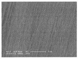
图3是碳纳米管拉膜的扫描电镜照片。Fig. 3 is a scanning electron micrograph of a carbon nanotube drawn film.
图4是碳纳米管碾压膜的扫描电镜照片。Fig. 4 is a scanning electron micrograph of a carbon nanotube rolled film.
图5是碳纳米管絮化膜的扫描电镜照片。Fig. 5 is a scanning electron micrograph of a carbon nanotube flocculated film.
图6是长碳纳米管膜的扫描电镜照片。Fig. 6 is a scanning electron micrograph of a long carbon nanotube film.
图7是本发明第二实施例提供的热致变色元件的结构示意图。Fig. 7 is a schematic structural diagram of a thermochromic element provided by a second embodiment of the present invention.
图8是本发明第三实施例提供的热致变色元件的结构示意图。Fig. 8 is a schematic structural diagram of a thermochromic element provided by a third embodiment of the present invention.
图9是本发明第四实施例提供的热致变色元件的结构示意图;其中,复合材料的一角被切除,以显示其内部结构。Fig. 9 is a schematic structural view of the thermochromic element provided by the fourth embodiment of the present invention; wherein, a corner of the composite material is cut off to show its internal structure.
图10是本发明第五实施例提供的热致变色显示装置的结构示意图。FIG. 10 is a schematic structural diagram of a thermochromic display device provided by a fifth embodiment of the present invention.
具体实施方式 Detailed ways
下面将结合附图及具体实施例,对本发明提供的一种热致变色元件及热致变色显示装置作进一步的详细说明。A thermochromic element and a thermochromic display device provided by the present invention will be further described in detail below with reference to the accompanying drawings and specific embodiments.
请参阅图2,本发明第一实施例提供一种热致变色元件10,其包括一热致变色结构14、一加热结构16以及至少两电极18。所述热致变色结构14与该加热结构16对应设置。所述至少两电极18与加热结构16电连接,且该至少两电极18间隔设置。Please refer to FIG. 2 , the first embodiment of the present invention provides a
所述热致变色结构14在不同的温度下显示不同的颜色,可通过控制热致变色结构14的加热温度使该热致变色结构14显示不同的颜色。所述热致变色结构14的材料包括结构转变颜料、得失水转变颜料、配位数转变颜料以及液晶微囊颜料中的一种或多种。所述热致变色结构14材料也包括单色显示材料或多色显示材料。本实施例中,所述热致变色结构14的材料为热致变色液晶微囊颜料,该热致变色液晶微囊颜料在显色状态下显示宝石蓝色。The
所述加热结构16为热致变色结构14提供热源,使其在一定的温度下显示颜色。所述热致变色结构14与所述加热结构16对应设置。具体地,所述热致变色结构14设置于所述加热结构16的表面;或所述热致变色结构14与所述加热结构16间隔设置。本实施例中,所述热致变色结构14通过印刷、涂敷或喷洒等方法设置于该加热结构16的表面。所述加热结构16包括至少一碳纳米管结构。所述碳纳米管结构包括至少一碳纳米管膜。所述碳纳米管膜具有自支撑的特性,所述自支撑的特性是指碳纳米管膜无需通过一支撑体支撑,也能保持自身特定的形状的性质。所述碳纳米管膜为多个碳纳米管,该多个碳纳米管有序排列或无序排列。所述有序排列是指碳纳米管有规则排列。所述无序排列是指碳纳米管无规则排列。所述碳纳米管膜为碳纳米管拉膜、碳纳米管碾压膜、絮化膜或长碳纳米管膜。The
请参阅图3,所述碳纳米管拉膜包括多个择优取向排列的碳纳米管。所述碳纳米管通过范德华力首尾相连。具体地,所述碳纳米管拉膜包括多个连续且定向排列的碳纳米管片段。该多个碳纳米管片段通过范德华力首尾相连。每一碳纳米管片段包括多个相互平行的碳纳米管,该多个相互平行的碳纳米管通过范德华力紧密结合。该碳纳米管片段具有任意的长度、厚度、均匀性及形状。该碳纳米管拉膜中的碳纳米管沿同一方向择优取向排列。所述碳纳米管拉膜可采用直接拉伸一碳纳米管阵列的方式获得,其中,该碳纳米管拉膜中的碳纳米管排列方向与其拉伸方向相同。所述碳纳米管拉膜的宽度与碳纳米管阵列所生长的基底的尺寸有关,该碳纳米管拉膜的厚度及长度不限,可根据实际需求制得。本实施例中,所述碳纳米管拉膜的厚度为0.5纳米~100微米,该碳纳米管拉膜的宽度为0.5纳米~10厘米。进一步地,所述碳纳米管结构包括至少两个重叠设置的碳纳米管拉膜,相邻两层碳纳米管拉膜中的碳纳米管之间具有一交叉角度α,且0°≤α≤90°。所述碳纳米管结构及其制备方法请参阅范守善等人于2007年2月9日申请的,公开日为2008年8月13日,公开号为CN101239712A,标题为“碳纳米管薄膜结构及其制备方法”的中国专利申请。Please refer to FIG. 3 , the drawn carbon nanotube film includes a plurality of carbon nanotubes arranged in preferred orientations. The carbon nanotubes are connected end to end by van der Waals forces. Specifically, the drawn carbon nanotube film includes a plurality of continuous and aligned carbon nanotube segments. The plurality of carbon nanotube segments are connected end to end by van der Waals force. Each carbon nanotube segment includes a plurality of parallel carbon nanotubes, and the plurality of parallel carbon nanotubes are closely combined by van der Waals force. The carbon nanotube segment has any length, thickness, uniformity and shape. The carbon nanotubes in the carbon nanotube stretched film are preferentially aligned along the same direction. The carbon nanotube stretched film can be obtained by directly stretching a carbon nanotube array, wherein the arrangement direction of the carbon nanotubes in the carbon nanotube stretched film is the same as the stretching direction. The width of the drawn carbon nanotube film is related to the size of the substrate on which the carbon nanotube array grows. The thickness and length of the drawn carbon nanotube film are not limited and can be produced according to actual needs. In this embodiment, the thickness of the drawn carbon nanotube film is 0.5 nanometers to 100 microns, and the width of the drawn carbon nanotube film is 0.5 nanometers to 10 centimeters. Further, the carbon nanotube structure includes at least two overlapping carbon nanotube drawn films, and there is a crossing angle α between carbon nanotubes in two adjacent layers of carbon nanotube drawn films, and 0°≤α≤ 90°. For the carbon nanotube structure and its preparation method, please refer to the application of Fan Shoushan et al. on February 9, 2007, the publication date is August 13, 2008, the publication number is CN101239712A, and the title is "Carbon nanotube thin film structure and its Chinese patent application for preparation method".
请参阅图4,所述碳纳米管碾压膜包括多个均匀分布的碳纳米管,碳纳米管各向同性,沿同一方向或不同方向择优取向排列。所述碳纳米管碾压膜中的碳纳米管相互交叠。所述碳纳米管碾压膜可通过碾压一碳纳米管阵列获得。所述碳纳米管碾压膜的长度和宽度不限。所述碳纳米管碾压膜的厚度为1微米~1毫米。所述碳纳米管碾压膜的结构及其制备方法请参阅范守善等人于2007年6月1日申请的,申请号为200710074699.6,标题为“碳纳米管薄膜的制备方法”的中国专利申请。Please refer to FIG. 4 , the carbon nanotube rolling film includes a plurality of uniformly distributed carbon nanotubes, the carbon nanotubes are isotropic, and are aligned along the same direction or in different directions. The carbon nanotubes in the carbon nanotube rolled film overlap each other. The carbon nanotube rolled film can be obtained by rolling a carbon nanotube array. The length and width of the carbon nanotube rolled film are not limited. The carbon nanotube rolling film has a thickness of 1 micron to 1 mm. For the structure and preparation method of the carbon nanotube rolled film, please refer to the Chinese patent application filed by Fan Shoushan et al. on June 1, 2007, the application number is 200710074699.6, and the title is "Preparation method of carbon nanotube film".
请参阅图5,所述碳纳米管絮化膜包括多个相互缠绕的碳纳米管,通过范德华力相互吸引、缠绕,形成网络状结构。所述碳纳米管絮化膜各向同性。所述碳纳米管絮化膜中的碳纳米管为均匀分布,无规则排列。所述碳纳米管絮化膜的长度和宽度不限。所述碳纳米管絮化膜的结构及制备方法请参阅范守善等人于2007年4月13日申请的,申请号为200710074027.5,标题为“碳纳米管薄膜的制备方法”的中国专利申请。Please refer to FIG. 5 , the carbon nanotube flocculation film includes a plurality of intertwined carbon nanotubes, which attract and intertwine with each other through van der Waals force to form a network structure. The carbon nanotube flocculation film is isotropic. The carbon nanotubes in the carbon nanotube flocculated film are uniformly distributed and randomly arranged. The length and width of the carbon nanotube flocculated film are not limited. For the structure and preparation method of the carbon nanotube flocculation film, please refer to the Chinese patent application filed by Fan Shoushan et al. on April 13, 2007, the application number is 200710074027.5, and the title is "Preparation method of carbon nanotube film".
请参阅图6,所述长碳纳米管膜包括多个择优取向排列的碳纳米管。该多个碳纳米管之间相互平行,并排设置且通过范德华力紧密结合。该多个碳纳米管具有大致相等的长度,且其长度可达到厘米量级。所述长碳纳米管膜的长度可与碳纳米管的长度相等。所述长碳纳米管膜的长度受碳纳米管的长度的限制。所述长碳纳米管膜的结构及其制备方法请参阅范守善等人于2008年2月1日申请的,申请号为200810066048.7,标题为“碳纳米管薄膜结构及其制备方法”的中国专利申请。Please refer to FIG. 6 , the long carbon nanotube film includes a plurality of carbon nanotubes arranged in preferred orientations. The plurality of carbon nanotubes are parallel to each other, arranged side by side and tightly combined by van der Waals force. The plurality of carbon nanotubes have roughly the same length, and the length can reach centimeter level. The length of the long carbon nanotube film may be equal to the length of the carbon nanotubes. The length of the long carbon nanotube film is limited by the length of the carbon nanotubes. For the structure and preparation method of the long carbon nanotube film, please refer to the Chinese patent application filed by Fan Shoushan et al. on February 1, 2008, the application number is 200810066048.7, and the title is "carbon nanotube film structure and its preparation method" .
所述碳纳米管包括单壁碳纳米管、双壁碳纳米管和多壁碳纳米管中的一种或多种。所述单壁碳纳米管的直径为0.5纳米~50纳米,双壁碳纳米管的直径为1纳米~50纳米,多壁碳纳米管的直径为1.5纳米~50纳米。The carbon nanotubes include one or more of single-wall carbon nanotubes, double-wall carbon nanotubes and multi-wall carbon nanotubes. The single-walled carbon nanotubes have a diameter of 0.5 nm to 50 nm, the double-walled carbon nanotubes have a diameter of 1 nm to 50 nm, and the multi-walled carbon nanotubes have a diameter of 1.5 nm to 50 nm.
所述加热结构16的长度、宽度和厚度不限,可根据所述热致变色元件10的需要选择。本实施例中,所述加热结构16的长度为1厘米~10厘米,宽度为0.01厘米~10厘米,厚度为0.5纳米~2毫米。所述加热结构16优选为一碳纳米管拉膜,该碳纳米管膜中的碳纳米管优选为多壁碳纳米管,该多壁碳纳米管的直径为1.5纳米~50纳米。所述该碳纳米管膜的单位面积热容小于1.7×10⁻⁶焦耳每平方厘米开尔文,该碳纳米管膜在1.25毫秒就可实现从常温加热至1500开尔文。The length, width and thickness of the
所述至少两电极18与加热结构16电连接,且该至少两电极18间隔设置。所述至少两电极18设置于加热结构16的表面。具体地,该至少两电极18可以设置在加热结构16的同一表面上也可以设置在加热结构16的不同表面上。其中,该至少两电极18间隔设置,以使加热结构16应用于热致变色元件10时接入一定的阻值避免短路现象产生。所述至少两电极18为所述加热结构16提供电压,使该加热结构16产生热量。The at least two
所述至少两电极18由导电材料组成,该至少两电极18的形状不限,可为导电薄膜、金属片或者金属引线。优选地,至少两电极18均为一层导电薄膜。该导电薄膜的厚度为0.5纳米~100微米。该导电薄膜的材料可以为金属、合金、铟锡氧化物(ITO)、锑锡氧化物(ATO)、导电银胶、或导电聚合物等。该金属或合金材料可以为铝、铜、钨、钼、金、钛、银、钕、钯、铯或其任意组合的合金。本实施例中,所述至少两电极18的材料为金属钯膜,厚度为5纳米。所述金属钯与碳纳米管具有较好的润湿效果,有利于所述至少两电极18与所述加热结构16之间形成良好的电接触,减少欧姆接触电阻。The at least two
此外,由于碳纳米管结构具有较大的比表面积,其本身有很好的粘附性,故由碳纳米管结构组成的加热结构16直接就可以与至少两电极18之间形成很好的电接触。另外,所述的至少两电极18也可通过一导电粘结剂(图未示)设置于该加热结构16的表面上,该导电粘结剂在实现至少两电极18与加热结构16电接触的同时,还可以将所述至少两电极18更好地固定于加热结构16的表面上。本实施例优选的导电粘结剂为银胶。In addition, since the carbon nanotube structure has a large specific surface area and has good adhesion, the
所述热致变色元件10工作时,于所述至少两电极18施加一电压,该电压则作用于所述加热结构16上,所述加热结构16在该电压的作用下会有热量产生,该热量直接加热所述热致变色结构14。随着热量的不同,所述热致变色结构14就会显示不同的颜色。由于本实施例中采用碳纳米管拉膜作为加热结构16,而碳纳米管拉膜具有较小的单位面积热容,所以该加热结构16具有升温迅速、热滞后小、热交换速度快的特点;因此,该热致变色元件10具有显色响应较快、能耗小的优点。此外,碳纳米管拉膜为一面状结构,与线状结构相比,碳纳米管膜与所述热致变色结构14的接触面积较大,其工作时能够使该热致变色结构14均匀受热,从而提高该热致变色元件10的清晰度,增加显示效率,而且较容易实现大面积显示图案及制备大面积的热致变色元件10,以利于该热致变色元件10在较大范围内的应用。另外,碳纳米管拉膜具有独立自支撑的特点,不需要支撑体支撑该加热结构16,避免支撑体吸收热量,以提高加热结构16的电热转换效率。When the
请参阅图7,本发明第二实施例提供一种热致变色元件30,其包括一热致变色结构34、一加热结构36以及至少两电极38。所述热致变色结构34与所述加热结构36对应设置。所述至少两电极38与加热结构36电连接,且该至少两电极38间隔设置。Please refer to FIG. 7 , the second embodiment of the present invention provides a
所述热致变色元件30与第一实施例提供的热致变色元件10的结构基本相同,其不同之处在于:所述热致变色结构34与所述加热结构36间隔设置。其中,所述热致变色元件30进一步包括一支撑体342,所述热致变色结构34通过印刷或喷涂等方法设置于该支撑体342的表面。具体地,所述热致变色结构34与所述加热结构36悬空设置;或所述支撑体342设置于所述热致变色结构34与所述加热结构36之间,且与该加热结构36贴合设置。本实施例中,所述热致变色结构34与所述加热结构36悬空设置,所述热致变色元件30进一步包括一固定体32,该固定体32设置于所述支撑体342及所述加热结构36的边缘,以固定该支撑体342及该加热结构36。所述固定体32及支撑体342的形状及大小不限,可依据实际需要进行改变。该固定体32及支撑体342的材料分别为陶瓷、玻璃、树脂、石英、塑料或纤维等。本实施例中,该固定体32的材料为塑料,该支撑体342的材料为玻璃。The structure of the
请参阅图8,本发明第三实施例提供一种热致变色元件40,其包括一热致变色结构44、一加热结构46以及至少两电极48。所述至少两电极48设置于所述加热结构46的表面,且该至少两电极48间隔设置。Please refer to FIG. 8 , the third embodiment of the present invention provides a
所述热致变色元件40与第一实施例提供的热致变色元件10的结构基本相同,其不同之处在于:所述加热结构46包括一第一碳纳米管膜462及一第二碳纳米管膜464。所述第一碳纳米管膜462、所述热致变色结构44、所述第二碳纳米管膜464依次堆叠设置,即所述热致变色结构44设置于所述第一碳纳米管膜462与第二碳纳米管膜464之间。所述至少两电极48设置于第一碳纳米管膜462与第二碳纳米管膜464之间,并与该第一碳纳米管膜462与第二碳纳米管膜464电连接。这样,可以使加热结构46产生的热量较快的传递给热致变色结构44,从而热致变色结构44的显色响应较快,进而提高热致变色元件40的显色响应的灵敏度。所述至少两电极48与所述热致变色结构44可以接触设置,也可以间隔设置。本实施例中,所述至少两电极48与热致变色结构44间隔设置。The structure of the
请参阅图9,本发明第四实施例提供一种热致变色元件50,其包括一复合材料56以及至少两电极58。所述至少两电极58与所述复合材料56电连接,且该至少两电极58间隔设置。Referring to FIG. 9 , the fourth embodiment of the present invention provides a
所述热致变色元件50与第一实施例提供的热致变色元件10的结构基本相同,其不同之处在于:所述热致变色结构54植入加热结构52中,形成所述复合材料56。该复合材料56既具有加热的性质,又具有显色的性质。这是由于加热结构52具有微孔结构,所述热致变色结构54分布于加热结构52的微孔结构中。由于所述热致变色结构54分布于加热结构52的微孔结构中,当加热结构56被施加一电压时,加热结构52产生的热量迅速被该热致变色结构54吸收,加快了该热致变色结构54的显色响应速率,从而使得该热致变色元件50的显色响应更灵敏。The structure of the
请参阅图10,本发明第五实施例提供一使用图1所示的热致变色元件10的热致变色显示装置200。所述热致变色显示装置200包括一绝缘体202,多个热致变色显示单元220设置于该绝缘体202表面,以及多个行电极引线204与多个列电极引线206设置于该绝缘体202表面。所述多个行电极引线204与列电极引线206分别平行且等间隔设置于绝缘体202表面上。所述多个行电极引线204与多个列电极引线206相互交叉设置,而且,在行电极引线204与列电极引线206交叉处设置有一介质绝缘层216,该介质绝缘层216将行电极引线204与列电极引线206电隔离,以防止短路。每两个相邻的行电极引线204与每两个相邻的列电极引线206形成一网格214,且每个网格214定位一个热致变色显示单元220。Please refer to FIG. 10 , the fifth embodiment of the present invention provides a
所述多个热致变色显示单元220对应设置于上述网格214中,且每个网格214中设置一个热致变色显示单元220。每个热致变色显示单元220包括一热致变色元件10、一第一电极210,以及一第二电极212。所述热致变色元件10包括一热致变色结构14及一加热结构16。每一行的网格214中的第一电极210与同一行电极引线204电连接,每一列的网格中214的第二电极212与同一列电极引线206电连接。所述第一电极210与第二电极212间隔设置于每个网格214中,并与所述加热结构16电连接。所述热致变色元件10与绝缘体202贴合设置或间隔设置。本实施例中,同一行的热致变色显示单元220中的第一电极210与同一行电极引线204电连接,同一列的热致变色显示单元220中的第二电极212与同一列电极引线206电连接。所述热致变色元件10与绝缘体202间隔设置;具体地,所述加热结构16与绝缘体202间隔设置。The plurality of
所述绝缘体202为一绝缘基底,其材料可为硬性材料,如:陶瓷、玻璃、树脂、石英等;其亦可为柔性材料,如:塑料或纤维等。当所述绝缘体202为柔性材料时,该热致变色显示装置200在使用时可根据需要弯折成任意形状。其中,所述绝缘体202的大小不限,本领域技术人员可依据实际需要进行选择。本实施例中,绝缘体202优选为一玻璃绝缘基底,其厚度为大于1毫米,长度为3厘米,宽度为2厘米。进一步,所述绝缘体202的表面具有多个对应于所述网格214设置的凹槽。该凹槽等大且等间隔地分布于所述绝缘体202表面。所述加热结构16通过所述绝缘体202表面的凹槽与所述绝缘体202间隔设置,减少该绝缘体202吸收该加热结构16产生的热量,使得所述热致变色结构14升温与降温都比较好,从而使该热致变色结构14显色响应更快,进而使所述热致变色显示装置200具有良好的显色响应能力及较小的能量损失。The
所述多个行电极引线204与多个列电极引线206为导电体,如金属层等。该多个行电极引线204与多个列电极引线206的行距和列距可以根据实际需要选择。该行电极引线204与列电极引线206的交叉角度为10度到90度。本实施例中,该多个行电极引线204与多个列电极引线206优选为采用导电浆料印制的平面导电体,且该多个行电极引线204与多个列电极引线206的行距和列距为300微米~500微米。该行电极引线204与列电极引线206的宽度为30微米~100微米,厚度为10微米~50微米。该行电极引线204与列电极引线206的交叉角度优选为90度。通过丝网印刷法将导电浆料印制于绝缘体202上制备行电极引线204与列电极引线206。该导电浆料的成分包括金属粉、低熔点玻璃粉和粘结剂。其中,该金属粉优选为银粉,该粘结剂优选为松油醇或乙基纤维素。该导电浆料中,金属粉的重量比为50~90%,低熔点玻璃粉的重量比为2~10%,粘结剂的重量比为10~40%。The plurality of row electrode leads 204 and the plurality of column electrode leads 206 are conductors, such as metal layers. The row spacing and column spacing of the plurality of row electrode leads 204 and the plurality of column electrode leads 206 can be selected according to actual needs. The intersection angle of the
所述第一电极210与第二电极212为导电体,如金属层等。该第一电极210与第二电极212为平面导电体,其尺寸以及该两电极之间的间距依据网格214的尺寸决定,具体地根据行列电极之间的间距而定。该第一电极210直接与所述行电极引线204连接,以实现电连接;该第二电极212直接与所述列电极引线206连接,以实现电连接。本实施例中,所述第一电极210与第二电极212的长度分别优选为60微米、70微米,宽度均优选为40微米,厚度均优选为20微米。所述第一电极210与第二电极212之间的间隔距离为250微米。所述第一电极210与第二电极212的材料为导电浆料,通过丝网印刷法印制于绝缘体202上。该导电浆料的成分与上述电极引线所用的导电浆料的成分相同。The
所述热致变色元件10采用本发明第一实施例提供的热致变色元件10。所述热致变色元件10之加热结构16与所述第一电极210和第二电极212的电连接方式可以为通过一导电胶电连接,也可以通过分子间力或者其他方式实现。所述加热结构16的材料为碳纳米管膜,将至少一碳纳米管膜采用铺设法直接铺设于上述含有多个行电极引线204、多个列电极引线206、多个第一电极210及多个第二电极212的绝缘体202上,该制作方法不需要预先设计或处理碳纳米管膜,方法比较简单。所述热致变色显示装置200中的各个热致变色元件10之热致变色结构14的材料可以相同,也可以不同。本实施例中,所述热致变色显示装置200中的各个热致变色元件10之热致变色结构14的材料均为宝石蓝材料。The
另外,所述热致变色显示装置200的每个热致变色显示单元220可以进一步包括至少一固定电极设置于所述第一电极210或第二电极212中的至少一个电极的表面,且与所述加热结构16电连接。该至少一固定电极是为了将所述热致变色元件10固定于所述第一电极210或第二电极212中的至少一个电极的表面。In addition, each
所述热致变色显示装置200工作时,于所述多个行电极引线204与多个列电极引线206施加一电压,该多个热致变色显示单元220中的第一电极210及第二电极212之间产生一电压,该电压进而作用于所述热致变色元件10之加热结构16上,该加热结构16就会有热量产生以均匀加热该热致变色结构14,使整个热致变色元件10都能显色。该热致变色结构14在加热状态下,随着加热温度的变化显示不同的颜色。通过一程序控制每个热致变色显示单元220显示一种颜色的时间,使每个热致变色显示单元220中的热致变色元件10之热致变色结构14的颜色转换频率大于25赫兹,这样该热致变色显示装置200就可以显示各种不同的图像。由于该热致变色元件10整个元件都能显色,显示效果比较明显,图像比较清晰。When the
本发明实施例提供的热致变色元件及热致变色显示装置具有以下优点:第一,所述加热结构包括至少一碳纳米管膜,该碳纳米管膜中的碳纳米管均匀分布,故该碳纳米管膜具有较均匀的厚度及电阻,发热均匀;因此可以给热致变色结构提供稳定的热源,使得显色均匀、稳定。第二,由于碳纳米管膜的厚度及单位面积热容较小,所以该碳纳米管膜可以提供的热量的改变比较明显,所以由碳纳米管膜组成的加热结构具有升温迅速、热滞后小、热交换速度快的特点;因此,所述热致变色元件具有颜色显色响应较快、能耗小的优点;进一步,使用该热致变色元件的热致变色显示装置具有图像反应灵敏、能耗小的优点。第三,该热致变色显示装置通过控制行电极引线与列电极引线来控制显示所述第一电极及第二电极,进而控制所述加热结构,从而实现对特定微小区域的加热,使得该热致变色显示装置具有显示清晰的特点。第四,碳纳米管膜为一面状结构,可以比较方便地应用于热致变色元件及其显示装置中,尤其是大面积的热致变色元件及其显示装置;实现热致变色元件在较大范围内的应用。第五,碳纳米管膜为一面状结构,其工作时能够使热致变色结构均匀受热,从而提高该热致变色元件的清晰度,增加显示效率,进而使得该热致变色装置具有清晰度及显示效率较高的优点。The thermochromic element and thermochromic display device provided by the embodiments of the present invention have the following advantages: first, the heating structure includes at least one carbon nanotube film, and the carbon nanotubes in the carbon nanotube film are uniformly distributed, so the The carbon nanotube film has relatively uniform thickness and resistance, and generates heat evenly; therefore, it can provide a stable heat source for the thermochromic structure, making the color development uniform and stable. Second, due to the small thickness and heat capacity per unit area of the carbon nanotube film, the change of the heat that the carbon nanotube film can provide is more obvious, so the heating structure composed of the carbon nanotube film has the characteristics of rapid temperature rise and small thermal hysteresis. , the characteristics of fast heat exchange; therefore, the thermochromic element has the advantages of fast color response and low energy consumption; further, the thermochromic display device using the thermochromic element has a sensitive image response, energy The advantage of low consumption. Third, the thermochromic display device controls the display of the first electrode and the second electrode by controlling the row electrode lead and the column electrode lead, and then controls the heating structure, so as to realize the heating of a specific micro region, so that the heat The chromic display device has the characteristic of clear display. Fourth, the carbon nanotube film has a planar structure, which can be more conveniently applied to thermochromic elements and their display devices, especially large-area thermochromic elements and their display devices; applications within the range. Fifth, the carbon nanotube film has a planar structure, which can make the thermochromic structure evenly heated during operation, thereby improving the clarity of the thermochromic element and increasing the display efficiency, thereby enabling the thermochromic device to have clarity and Shows the advantage of higher efficiency.
另外,本领域技术人员还可以在本发明精神内做其它变化,这些依据本发明精神所做的变化,都应包含在本发明所要求保护的范围内。In addition, those skilled in the art can also make other changes within the spirit of the present invention, and these changes made according to the spirit of the present invention should be included in the scope of protection claimed by the present invention.
Claims (10)
Priority Applications (3)
| Application Number | Priority Date | Filing Date | Title |
|---|---|---|---|
| CN200910105810.2A CN101819335B (en) | 2009-02-27 | 2009-02-27 | Thermochromatic element and thermochromatic display device |
| US12/589,478 US7933058B2 (en) | 2009-02-27 | 2009-10-22 | Thermochromic component and thermochromic display apparatus using the same |
| JP2010020348A JP5255005B2 (en) | 2009-02-27 | 2010-02-01 | Thermochromic element and display device using the same |
Applications Claiming Priority (1)
| Application Number | Priority Date | Filing Date | Title |
|---|---|---|---|
| CN200910105810.2A CN101819335B (en) | 2009-02-27 | 2009-02-27 | Thermochromatic element and thermochromatic display device |
Publications (2)
| Publication Number | Publication Date |
|---|---|
| CN101819335A CN101819335A (en) | 2010-09-01 |
| CN101819335B true CN101819335B (en) | 2014-01-15 |
Family
ID=42654493
Family Applications (1)
| Application Number | Title | Priority Date | Filing Date |
|---|---|---|---|
| CN200910105810.2A Expired - Fee Related CN101819335B (en) | 2009-02-27 | 2009-02-27 | Thermochromatic element and thermochromatic display device |
Country Status (3)
| Country | Link |
|---|---|
| US (1) | US7933058B2 (en) |
| JP (1) | JP5255005B2 (en) |
| CN (1) | CN101819335B (en) |
Families Citing this family (22)
| Publication number | Priority date | Publication date | Assignee | Title |
|---|---|---|---|---|
| CN101847345B (en) * | 2009-03-27 | 2012-07-18 | 清华大学 | Incandescent light source display device and manufacture method thereof |
| CN102087101B (en) * | 2009-12-04 | 2012-07-18 | 清华大学 | Device and method for measuring strain |
| CN102116943B (en) * | 2009-12-31 | 2013-02-13 | 清华大学 | Thermotropic display element and thermotropic display device |
| CN102116942B (en) * | 2009-12-31 | 2013-02-13 | 清华大学 | Thermal display component and thermal display device |
| US8432602B2 (en) * | 2010-06-24 | 2013-04-30 | Tsinghua University | Chromatic element and chromatic display device using the same |
| CN101880035A (en) | 2010-06-29 | 2010-11-10 | 清华大学 | carbon nanotube structure |
| KR101225900B1 (en) * | 2011-04-28 | 2013-01-24 | 이효제 | Heat And Light Emitting Display |
| FR2987122B1 (en) * | 2012-02-16 | 2014-03-21 | Commissariat Energie Atomique | DISPLAY SCREEN AND METHOD FOR MANUFACTURING THE SAME |
| CN103728743B (en) * | 2012-10-15 | 2017-02-01 | 北京富纳特创新科技有限公司 | Thermochromism display element and thermochromism display device |
| CN103728742B (en) * | 2012-10-15 | 2017-01-18 | 北京富纳特创新科技有限公司 | Thermochromism display element and thermochromism display device |
| CN103728741B (en) * | 2012-10-15 | 2016-08-10 | 北京富纳特创新科技有限公司 | Thermochromatic element and thermochromatic display device |
| CN103885209B (en) * | 2012-12-22 | 2016-08-10 | 清华大学 | Thermochromatic element and thermochromatic display device |
| DE112016001642T5 (en) * | 2015-04-07 | 2018-01-04 | Denso Corporation | Heating device |
| KR101810066B1 (en) * | 2016-04-15 | 2017-12-20 | 한국과학기술원 | Thermochromic display device using acoustothermal heating |
| KR102713078B1 (en) | 2017-01-16 | 2024-10-02 | 엘지디스플레이 주식회사 | Contact sensitive device |
| CN107153305B (en) * | 2017-07-13 | 2020-01-10 | 京东方科技集团股份有限公司 | Spacer and manufacturing method thereof |
| CN107539012B (en) * | 2017-08-28 | 2019-10-25 | 福建师范大学 | Flexible heat-sensitive color-changing composite material and heat-sensitive pattern making device |
| CN107479216B (en) * | 2017-08-28 | 2020-07-10 | 福建师范大学 | Thermochromic elements, thermochromic actuators and plant protection devices |
| CN112992084A (en) * | 2019-12-16 | 2021-06-18 | 上海航空电器有限公司 | Pixelized warm color liquid crystal array system for optical stealth |
| CN113029395B (en) * | 2021-03-05 | 2021-10-29 | 中国人民解放军国防科技大学 | Transient high-temperature field heat flux passive sensor based on thermosensitive coating color change characteristic |
| KR20230013688A (en) * | 2021-07-16 | 2023-01-27 | 삼성디스플레이 주식회사 | Display device and manufacturing method for the same |
| CN114236811B (en) * | 2021-12-20 | 2024-11-26 | 北京京东方技术开发有限公司 | A reflective electrochromic material, display device, manufacturing and driving method |
Citations (4)
| Publication number | Priority date | Publication date | Assignee | Title |
|---|---|---|---|---|
| US5202677A (en) * | 1991-01-31 | 1993-04-13 | Crystal Images, Inc. | Display apparatus using thermochromic material |
| WO2004082333A1 (en) * | 2003-03-14 | 2004-09-23 | Nanotech Co., Ltd. | Seat-like heating units with porous plate-shaped electrode |
| KR20080070204A (en) * | 2007-01-25 | 2008-07-30 | 삼성전자주식회사 | Display using thermochromic material |
| CN101239712A (en) * | 2007-02-09 | 2008-08-13 | 清华大学 | Carbon nanotube film structure and preparation method thereof |
Family Cites Families (14)
| Publication number | Priority date | Publication date | Assignee | Title |
|---|---|---|---|---|
| JPS5697381A (en) * | 1980-01-07 | 1981-08-06 | Oki Electric Ind Co Ltd | Display unit |
| SE9301601D0 (en) * | 1993-05-10 | 1993-05-10 | Larson Brothers Co Ab | METHOD AND APPROACH TO VISUALIZE PATTERNS |
| JP2563765B2 (en) * | 1994-12-05 | 1996-12-18 | 沖電気工業株式会社 | Display device |
| SE515437C2 (en) * | 1997-10-22 | 2001-08-06 | Lars Andersson | Figure Painting |
| US7164224B2 (en) * | 2000-12-14 | 2007-01-16 | Sharp Kabushiki Kaisha | Backlight having discharge tube, reflector and heat conduction member contacting discharge tube |
| JP2004086736A (en) * | 2002-08-28 | 2004-03-18 | Toshiba Corp | Electronics |
| CN100411979C (en) | 2002-09-16 | 2008-08-20 | 清华大学 | A carbon nanotube rope and its manufacturing method |
| US20080297878A1 (en) * | 2003-10-01 | 2008-12-04 | Board Of Regents, The University Of Texas System | Compositions, methods and systems for making and using electronic paper |
| EP1814713A4 (en) | 2004-11-09 | 2017-07-26 | Board of Regents, The University of Texas System | The fabrication and application of nanofiber ribbons and sheets and twisted and non-twisted nanofiber yarns |
| CN100500556C (en) | 2005-12-16 | 2009-06-17 | 清华大学 | Carbon nano-tube filament and its production |
| JP4817296B2 (en) * | 2006-01-06 | 2011-11-16 | 独立行政法人産業技術総合研究所 | Aligned carbon nanotube bulk aggregate and method for producing the same |
| CN101314464B (en) | 2007-06-01 | 2012-03-14 | 北京富纳特创新科技有限公司 | Process for producing carbon nano-tube film |
| CN101353785B (en) * | 2007-07-25 | 2010-09-29 | 清华大学 | Preparation method of high-density carbon nanotube array composite material |
| CN101751916B (en) * | 2008-12-12 | 2012-12-19 | 清华大学 | Ultrasonic acoustic generator |
-
2009
- 2009-02-27 CN CN200910105810.2A patent/CN101819335B/en not_active Expired - Fee Related
- 2009-10-22 US US12/589,478 patent/US7933058B2/en active Active
-
2010
- 2010-02-01 JP JP2010020348A patent/JP5255005B2/en not_active Expired - Fee Related
Patent Citations (4)
| Publication number | Priority date | Publication date | Assignee | Title |
|---|---|---|---|---|
| US5202677A (en) * | 1991-01-31 | 1993-04-13 | Crystal Images, Inc. | Display apparatus using thermochromic material |
| WO2004082333A1 (en) * | 2003-03-14 | 2004-09-23 | Nanotech Co., Ltd. | Seat-like heating units with porous plate-shaped electrode |
| KR20080070204A (en) * | 2007-01-25 | 2008-07-30 | 삼성전자주식회사 | Display using thermochromic material |
| CN101239712A (en) * | 2007-02-09 | 2008-08-13 | 清华大学 | Carbon nanotube film structure and preparation method thereof |
Also Published As
| Publication number | Publication date |
|---|---|
| JP2010204648A (en) | 2010-09-16 |
| US7933058B2 (en) | 2011-04-26 |
| US20100220379A1 (en) | 2010-09-02 |
| JP5255005B2 (en) | 2013-08-07 |
| CN101819335A (en) | 2010-09-01 |
Similar Documents
| Publication | Publication Date | Title |
|---|---|---|
| CN101819335B (en) | Thermochromatic element and thermochromatic display device | |
| CN102103274B (en) | Thermochromic element and thermochromic display device | |
| CN102103276B (en) | Thermochromatic element and thermochromatic display device | |
| CN102103275B (en) | Thermochromatic element and thermochromatic display device | |
| CN101848564A (en) | Heating element | |
| CN103728741B (en) | Thermochromatic element and thermochromatic display device | |
| CN103885209B (en) | Thermochromatic element and thermochromatic display device | |
| CN101868069B (en) | Plane heat source | |
| CN101616513B (en) | Linear heat source | |
| TWI454817B (en) | Thermochromic element and thermochromic display device | |
| TWI487970B (en) | Thermal display element and thermal display device | |
| TWI598857B (en) | Thermochromic element and thermochromic display device | |
| TWI487971B (en) | Thermal display element and thermal display device | |
| CN101636007B (en) | Plane heat source | |
| TWI387834B (en) | Thermochromic element and thermochromic display device | |
| CN103728742B (en) | Thermochromism display element and thermochromism display device | |
| CN101636008B (en) | Plane heat source | |
| CN101636011B (en) | Hollow heat source | |
| CN101616512B (en) | Line heat source | |
| CN101616516B (en) | Line heat source | |
| CN101626642B (en) | Hollow heat source | |
| TWI381989B (en) | Heating device | |
| TWI360831B (en) | Field emission electron device | |
| TWI380728B (en) | Linear heater | |
| TW201133426A (en) | Thermochromatic device and thermochromatic display apparatus |
Legal Events
| Date | Code | Title | Description |
|---|---|---|---|
| C06 | Publication | ||
| PB01 | Publication | ||
| C10 | Entry into substantive examination | ||
| SE01 | Entry into force of request for substantive examination | ||
| C14 | Grant of patent or utility model | ||
| GR01 | Patent grant | ||
| CF01 | Termination of patent right due to non-payment of annual fee |
Granted publication date: 20140115 |
|
| CF01 | Termination of patent right due to non-payment of annual fee |