WO2025042702A1 - Article with a substrate and multilayer coating on the substrate and solar panel incorporating the article - Google Patents
Article with a substrate and multilayer coating on the substrate and solar panel incorporating the article Download PDFInfo
- Publication number
- WO2025042702A1 WO2025042702A1 PCT/US2024/042603 US2024042603W WO2025042702A1 WO 2025042702 A1 WO2025042702 A1 WO 2025042702A1 US 2024042603 W US2024042603 W US 2024042603W WO 2025042702 A1 WO2025042702 A1 WO 2025042702A1
- Authority
- WO
- WIPO (PCT)
- Prior art keywords
- layer
- article
- refractive index
- range
- index material
- Prior art date
- Legal status (The legal status is an assumption and is not a legal conclusion. Google has not performed a legal analysis and makes no representation as to the accuracy of the status listed.)
- Pending
Links
Classifications
-
- C—CHEMISTRY; METALLURGY
- C03—GLASS; MINERAL OR SLAG WOOL
- C03C—CHEMICAL COMPOSITION OF GLASSES, GLAZES OR VITREOUS ENAMELS; SURFACE TREATMENT OF GLASS; SURFACE TREATMENT OF FIBRES OR FILAMENTS MADE FROM GLASS, MINERALS OR SLAGS; JOINING GLASS TO GLASS OR OTHER MATERIALS
- C03C17/00—Surface treatment of glass, not in the form of fibres or filaments, by coating
- C03C17/34—Surface treatment of glass, not in the form of fibres or filaments, by coating with at least two coatings having different compositions
- C03C17/3411—Surface treatment of glass, not in the form of fibres or filaments, by coating with at least two coatings having different compositions with at least two coatings of inorganic materials
- C03C17/3429—Surface treatment of glass, not in the form of fibres or filaments, by coating with at least two coatings having different compositions with at least two coatings of inorganic materials at least one of the coatings being a non-oxide coating
- C03C17/3435—Surface treatment of glass, not in the form of fibres or filaments, by coating with at least two coatings having different compositions with at least two coatings of inorganic materials at least one of the coatings being a non-oxide coating comprising a nitride, oxynitride, boronitride or carbonitride
-
- C—CHEMISTRY; METALLURGY
- C03—GLASS; MINERAL OR SLAG WOOL
- C03C—CHEMICAL COMPOSITION OF GLASSES, GLAZES OR VITREOUS ENAMELS; SURFACE TREATMENT OF GLASS; SURFACE TREATMENT OF FIBRES OR FILAMENTS MADE FROM GLASS, MINERALS OR SLAGS; JOINING GLASS TO GLASS OR OTHER MATERIALS
- C03C2217/00—Coatings on glass
- C03C2217/70—Properties of coatings
- C03C2217/73—Anti-reflective coatings with specific characteristics
- C03C2217/734—Anti-reflective coatings with specific characteristics comprising an alternation of high and low refractive indexes
Definitions
- This disclosure pertains to an article with a substrate and a multilayer coating on the substrate, where the article has an enhanced durability and reduced reflectance to achieve high transmittance of electromagnetic radiation having wavelengths within the range of from 600 nm to 750 nm, and more particularly, to a solar panel incorporating the article as a cover glass over photovoltaic cells.
- Electricity demand tends to increase as the human population of the Earth increases.
- carbon-based fuels have been utilized to generate electricity.
- the Earth’s reserves of carbon-based fuels are finite.
- Alternative ways to generate electricity have been developed and are in development, such as generating electricity from the Sun, from wind, from waves, from tidal changes, and so on.
- solar panels generate electricity from the Sun.
- Nuclear fusion and other processes at the Sun generate photons, which are packets of energy, spanning a broad range of wavelengths. These photons travel toward the Earth.
- Photons of certain wavelength ranges manage to penetrate the Earth’s atmosphere and reach the Earth’s surface.
- the photons from the Sun that reach the Earth’s surface correspond to wavelengths in the visible spectrum, the near-infrared spectrum, the infrared spectrum, the radio wave spectrum, and the ultraviolet spectrum, among others.
- the photons corresponding to the visible, near-infrared, and radio wave spectrums are the most abundant (see, e.g., FIG. 1).
- photons corresponding to the radio wave spectrum have much less energy per photon than photons corresponding to the visible and near-infrared spectrums (because energy per photon is inversely proportional to wavelength).
- solar panels include a semiconductor material that provides a photovoltaic effect that transforms photons into electricity.
- the semiconductor material absorbs the photons from the Sun. If the photon that the semiconductor material absorbs has sufficient energy, then the photon excites an electron to move from a relatively lower energy valence band to a relatively higher energy conduction band. The electron that moved to the conduction band leaves a “hole” in the valence band and thus a charge imbalance.
- the semiconductor material is connected to an electrical circuit, with appropriate doping and structure of the semiconductor material, such as in various combinations of n-doped and p-doped silicon regions arranged into junction structures known in the field of photovoltaics, the charge imbalance leads to electrical current.
- Whether the photon that the semiconductor material absorbs has sufficient energy to excite an electron to move from the valence band to the conduction band depends on the bandgap of the semiconductor material.
- Silicon for example, has a bandgap energy of about 1.1 electronvolts (eV), which corresponds to a photon having a wavelength of about 1100 nm, which is in the near-infrared spectrum.
- Photons having wavelengths of about 1100 nm and shorter (thus having higher energy per photon) when absorbed by the silicon semiconductor, excite the electron to move from the valence band to the conductive band.
- Other semiconductor materials have different bandgap energies. Photons that the semiconductor material absorb but do not excite electrons to the conductive band can generate heat. The heat generated can result in suboptimal solar panel electricity generation.
- solar panels In addition to a semiconductor material that converts photons into electricity, solar panels typically include a cover article over the semiconductor material.
- the cover article separates the semiconductor material from the external environment, such as rain, hail, debris, and other things that could damage the semiconductor material or wiring and electrical connections needed to efficiently harvest electricity from photovoltaic cells within the solar panel.
- the cover article sometimes includes a substrate having a glass composition.
- a typical glass-to-air interface reflects about 4% of incident electromagnetic radiation in the visible spectrum. The reflected photons cannot be used to generate electricity.
- the cover article sometimes includes an antireflection (AR) coating coated onto the surface of the substrate of glass.
- the AR coating is typically a porous layer of SiCh.
- the typical porous SiCh AR coating (i) lacks durability and (ii) exhibits suboptimal anti-reflectance. Regarding the lack of durability, the typical porous SiCh AR coating is readily removed via weather events, abrasion from dirt or sand, and cleaning. It is estimated that the typical porous SiCh AR coating is completely removed from the substrate after only five years of use and, in some cases, after only six months of use. The lack of durability is a problem because removal of the AR coating causes the substrate of glass to revert to its natural reflectance, and photons that otherwise could have been converted into electricity are reflected into the external environment.
- SiCh AR coatings are susceptible to scratches, chips, and partial delamination, which causes light scattering or multi-bounce reflection events resulting in an even higher reflectance (or lower transmittance) than if the substrate did not include the SiCh coating at all. These degradation mechanisms result in reduced electrical energy generation from the solar panel over time, which also leads to higher effective costs for electricity, which can be quantified as a higher levelized cost of energy over the life of the solar panel.
- a substrate of glass with the typical porous SiCh AR coating still reflects a considerable number of photons corresponding to the visual and near infrared spectrums.
- the cover article with the typical porous SiCh AR coating transmits photons associated with infrared wavelengths having energies less than the bandgap energy of the semiconductor material of the solar panel. While the semiconductor material does not absorb those photons and convert them to electricity, low levels of absorption in various layers of the solar panel (such as polymer encapsulants, metal contacts, etc.) can increase the temperature of the semiconductor and decrease electrical conversion efficiency.
- the present disclosure addresses the above-mentioned problems, and other problems, with an article that includes a substrate and a multilayer coating disposed on the substrate.
- the multilayer coating includes alternating layers of low refractive index material and high refractive index material, each layer having a unique thickness engineered so that the multilayer coating provides destructive interference at wavelengths in and around the range of 600 nm to 750 nm to increase transmittance thereof through the article. Increasing transmittance of photons associated with such a wavelength range increases the output of photovoltaic cells.
- the multilayer coating decreases transmittance of photons associated with wavelengths within a range of 300 nm to 350 nm and within a range of 1100 nm to 1800 nm.
- Photons of the former can degrade components of a solar panel which leads to lower electricity generation over time, while photons of the latter are unusable by the photovoltaic cells to generate electricity, because the photons have energies below the bandgap of silicon, and lead to thermal heating of the solar panel, which reduces the instantaneous electrical conversion efficiency of the solar panel.
- the multilayer coating imparts durability to the article, and the multilayer coatings are far more durable than incumbent porous coatings, meaning that the solar panels coated with the multilayer AR coatings of the present disclosure provide a higher electricity generation over time than solar panels coated with porous AR coatings.
- an article comprises: (i) a substrate comprising a first major surface and a second major surface; and (ii) a multilayer coating disposed on the first major surface of the substrate, the multilayer coating comprising at least one period of a layer of low refractive index material and a layer of high refractive index material, wherein, the article exhibits a prime surface average reflectance of less than or equal to 0.550% across an entire wavelength range of from 600 nm to 750 nm.
- the article of Aspect 1 is presented, wherein the substrate further comprises a glass composition or a glass-ceramic composition.
- the article of Aspect 2 is presented, wherein the glass composition is an alkali aluminosilicate glass composition, a soda lime glass composition, or an alkaline earth boro-aluminosilicate glass composition.
- the article of any one of Aspects 1 through 3 is presented, wherein (i) the low refractive index material has a refractive index within a range of from 1.40 to 1.60, and (ii) the high refractive index material has a refractive index within a range of from 1.70 to 2.50.
- the article of any one of Aspects 1 through 4 is presented, wherein (i) the low refractive index material is or comprises SiO 2 , doped SiO 2 , AI2O3, GeO 2 , SiO, A10 x N y , SiO x N y , Si u Al y O x N y , MgO, MgF 2 , BaF 2 , CaF 2 , DyF 3 , YbF 3 , YF 3 , and CeF 3 , and (ii) the high refractive index material is or comprises AIN, SiN x , A10 x N y , SiO x N y , or TiO 2 .
- the article of any one of Aspects 1 through 5 is presented, wherein the multilayer coating comprises a first layer of low refractive index material in direct contact with the first major surface, the first layer of low refractive index material having a thickness within a range of from 50 nm to 250 nm.
- the article of any one of Aspects 1 through 6 is presented, wherein the multilayer coating further comprises a total thickness that is within a range of from 350 nm to 1400 nm.
- the article of any one of Aspects 1 through 6 is presented, wherein the multilayer coating further comprises a total thickness that is within a range of from 350 nm to 800 nm.
- the article of any one of Aspects 1 through 6 is presented, wherein the multilayer coating further comprises a total thickness that is within a range of from 350 nm to 650 nm.
- the article of Aspect 10 is presented, wherein the thicknesses of the layers of low refractive index material combined comprise within a range of from 65% to 75% of the total thickness of the multilayer coating.
- Aspect 12 of the present disclosure the article of any one of Aspects 1 through 11 is presented, wherein the article exhibits a prime surface average reflectance of less than or equal to 2.0% across an entire wavelength range of from 400 nm to 450 nm.
- the article of any one of Aspects 1 through 12 is presented, wherein the article exhibits a prime surface average reflectance of less than or equal to 1.40% across an entire wavelength range of from 450 nm to 600 nm.
- Aspect 14 of the present disclosure the article of any one of Aspects 1 through 13 is presented, wherein the article exhibits a prime surface average reflectance of less than or equal to 0.730% across an entire wavelength range of from 750 nm to 800 nm.
- Aspect 15 of the present disclosure the article of any one of Aspects 1 through 14 is presented, wherein the article exhibits a prime surface average reflectance of less than or equal to 0.850% across an entire wavelength range of from 800 nm to 850 nm.
- Aspect 16 of the present disclosure the article of any one of Aspects 1 through 15 is presented, wherein the article exhibits a prime surface average reflectance of less than or equal to 1.05% across an entire wavelength range of from 850 nm to 900 nm.
- Aspect 18 of the present disclosure the article of any one of Aspects 1 through 17 is presented, wherein the article exhibits a prime surface average reflectance of less than or equal to 3.00% across an entire wavelength range of from 950 nm to 1000 nm.
- the article of any one of Aspects 1 through 18 is presented, wherein the article exhibits a prime surface average reflectance of less than or equal to 1.40% across an entire wavelength range of from 1000 nm to 1050 nm.
- the article of any one of Aspects 1 through 19 is presented, wherein the article exhibits a prime surface average reflectance of greater than or equal to 5.0% over one or more of the following wavelength ranges: from 1100 nm to 1200 nm, from 1200 nm to 1300 nm, from 1300 nm to 1400 nm, from 1400 nm to 1500 nm, from 1500 nm to 1600 nm, from 1600 nm to 1700 nm, or from 1700 nm to 1800 nm.
- the article of any one of Aspects 1 through 20 is presented, wherein the multilayer coating exhibits a maximum hardness of greater than or equal to 6 GPa measured over an indentation depth range from 0 to 125 nm according to a Berkovich Indenter Hardness Test.
- the article of any one of Aspects 1 through 20 is presented, wherein the multilayer coating exhibits a maximum hardness of greater than or equal to 8 GPa measured over an indentation depth range from 0 to 125 nm according to a Berkovich Indenter Hardness Test.
- the article of any one of Aspects 1 through 22 further comprises: an anti-soiling coating upon the multilayer coating, wherein (i) the anti-soiling coating comprises a silane or a siloxane material, and (ii) the anti-soiling coating exhibits hydrophobic, hydrophilic, or omniphobic properties.
- the article of any one of Aspects 1 through 22 further comprises: an anti-soiling coating upon the multilayer coating, wherein (a) the anti-soiling coating comprises (i) a silicon-containing matrix layer and (ii) a hydrophobic or hydrophilic surface modification material, and (b) the anti-soiling layer exhibits hydrophobic, hydrophilic, or omniphobic properties.
- an article comprises: (a) a substrate comprising a first major surface and a second major surface; and (b) a multilayer coating disposed on the first major surface of the substrate, the multilayer coating comprising (i) at least four layers, (ii) repeating periods of a layer of low refractive index material and a layer of high refractive index material, (iii) a total thickness that is within a range of from 350 nm to 1400 nm, (iv) a first layer of low refractive index material disposed directly on the first major surface of substrate, the first layer of low refractive index material comprising a thickness within a range of from 50 nm to 250 nm; wherein, thicknesses of the layers of low refractive index material combined comprise greater than 55% of the total thickness of the multilayer coating.
- the article of Aspect 25 is presented, wherein the substrate further comprises a glass composition or a glass-ceramic composition.
- the glass composition of the substrate is an alkali aluminosilicate glass composition, a soda lime glass composition, or an alkaline earth boro-aluminosilicate glass composition.
- the article of any one of Aspects 25 through 27 is presented, wherein the substrate comprises a region of compressive stress at or near the first major surface.
- the article of any one of Aspects 25 through 28 is presented, wherein the substrate comprises a thickness within a range of from 0.1 mm to 5.0 mm.
- the article of any one of Aspects 25 through 29 is presented, wherein (i) the low refractive index material has a refractive index within a range of from 1.40 to 1.60, and (ii) the high refractive index material has a refractive index within a range of from 1.70 to 2.50.
- the article of any one of Aspects 25 through 30 is presented, wherein (i) the low refractive index material is or comprises SiO 2 , doped SiO 2 , AI2O3, GeO 2 , SiO, A10 x N y , SiO x N y , Si u Al y O x N y , MgO, MgF 2 , BaF 2 , CaF 2 , DyF 3 , YbF 3 , YF 3 , and CeF 3 and (ii) the high refractive index material is or comprises AIN, SiN x , A10 x N y , SiO x N y , or TiO 2 .
- the low refractive index material is or comprises SiO 2 , doped SiO 2 , AI2O3, GeO 2 , SiO, A10 x N y , SiO x N y , Si u Al y O x N y , MgO, MgF 2 ,
- the article of any one of Aspects 25 through 31 is presented, wherein the layers of the low refractive index material comprise from 65% to 75% of the total thickness of the multilayer coating.
- the article of any one of Aspects 25 through 32 is presented, wherein the multilayer coating comprises (i) a first layer of low refractive index material disposed directly on the first major surface of the substrate, the first layer comprising a thickness within a range of from 175 nm to 225 nm, (ii) a second layer of high refractive index material disposed directly on the first layer, the second layer comprising a thickness within a range of from 15 nm to 25 nm, (iii) a third layer of low refractive index material disposed directly on the second layer, the third layer comprising a thickness within a range of from 30 nm to 40 nm, (iv) a fourth layer of high refractive index material disposed directly on the third layer, the fourth layer comprising a thickness within a range of from 130 nm to 150 nm, and (v) a fifth layer of low refractive index material disposed directly on the fourth layer, the fifth
- the article of any one of Aspects 25 through 32 is presented, wherein the multilayer coating comprises (i) a first layer of low refractive index material disposed directly on the first major surface of the substrate, the first layer comprising a thickness within a range of from 175 nm to 225 nm, (ii) a second layer of high refractive index material disposed directly on the first layer, the second layer comprising a thickness within a range of from 5 nm to 15 nm, (iii) a third layer of low refractive index material disposed directly on the second layer, the third layer comprising a thickness within a range of from 35 nm to 60 nm, (iv) a fourth layer of high refractive index material disposed directly on the third layer, the fourth layer comprising a thickness within a range of from 20 nm to 30 nm, (v) a fifth layer of low refractive index material disposed directly on the fourth layer, the fifth layer
- the article of any one of Aspects 25 through 32 is presented, wherein the multilayer coating comprises (i) a first layer of low refractive index material disposed directly on the first major surface of the substrate, the first layer comprising a thickness within a range of from 175 nm to 225 nm, (ii) a second layer of high refractive index material disposed directly on the first layer, the second layer comprising a thickness within a range of from 15 nm to 25 nm, (iii) a third layer of low refractive index material disposed directly on the second layer, the third layer comprising a thickness within a range of from 30 nm to 40 nm, (iv) a fourth layer of high refractive index material disposed directly on the third layer, the fourth layer comprising a thickness within a range of from 130 nm to 160 nm, (v) a fifth layer of low refractive index material disposed directly on the fourth layer, the fifth layer
- the article of any one of Aspects 25 through 35 is presented, wherein the article exhibits a prime surface average reflectance of less than or equal to 0.550% across an entire wavelength range of from 600 nm to 750 nm.
- the article of any one of Aspects 25 through 36 is presented, wherein the article exhibits: (i) a prime surface average reflectance of less than or equal to 2.0% across an entire wavelength range of from 400 nm to 450 nm, (ii) a prime surface average reflectance of less than or equal to 1.40% across an entire wavelength range of from 450 nm to 600 nm, (iii) a prime surface average reflectance of less than or equal to 0.730% across an entire wavelength range of from 750 nm to 800 nm, (iv) a prime surface average reflectance of less than or equal to 0.850% across an entire wavelength range of from 800 nm to 850 nm, (v) a prime surface average reflectance of less than or equal to 1.05% across an entire wavelength range of from 850 nm to 900 nm, (vi) a prime surface average reflectance of less than or equal to 2.20% across an entire wavelength range of from 900 n
- the article of any one of Aspects 25 through 37 is presented, wherein the article exhibits a prime surface average reflectance of greater than or equal to 5.0% over one or more of the following wavelength ranges: from 1100 nm to 1200 nm, from 1200 nm to 1300 nm, from 1300 nm to 1400 nm, from 1400 nm to 1500 nm, from 1500 nm to 1600 nm, from 1600 nm to 1700 nm, and from 1700 nm to 1800 nm.
- the article of any one of Aspects 25 through 38 is presented, wherein the multilayer coating exhibits a maximum hardness of greater than or equal to 6 GPa measured over an indentation depth range of from 0 to 125 nm according to a Berkovich Indenter Hardness Test.
- the article of any one of Aspects 25 through 38 is presented, wherein the multilayer coating exhibits a maximum hardness of greater than or equal to 8 GPa measured over an indentation depth range of from 0 to 125 nm according to a Berkovich Indenter Hardness Test.
- the article of any one of Aspects 25 through 40 further comprises: an anti through soiling coating upon the multilayer coating, wherein (i) the anti-soiling coating comprises a silane or a siloxane material, and (ii) the antisoiling coating exhibits hydrophobic, hydrophilic, or omniphobic properties.
- the article of any one of Aspects 25 through 40 further comprises: an anti-soiling coating upon the multilayer coating, wherein (a) the anti-soiling coating comprises (i) a silicon-containing matrix layer and (ii) a hydrophobic or hydrophilic surface modification material, and (b) the anti-soiling layer exhibits hydrophobic, hydrophilic, or omniphobic properties.
- a solar panel comprises: (1) an article comprising: (a) a substrate comprising a first major surface and a second major surface; and (b) a multilayer coating disposed on the first major surface of the substrate, the multilayer coating comprising repeating periods of a layer of low refractive index material and a layer of high refractive index material; wherein the article exhibits a prime surface average reflectance of less than or equal to 0.550% across an entire wavelength range of from 600 nm to 750 nm; and (2) an array of photovoltaic (PV) cells disposed beneath the second major surface of the substrate.
- PV photovoltaic
- the solar panel of Aspect 43 further comprises a backsheet, wherein, the array of PV cells is disposed between the backsheet and the article.
- the solar panel of Aspect 44 further comprises: (a) a package comprising the article, the array of PV cells, and the backsheet; and (b) a frame comprising (i) a sidewall extending around a perimeter of the package, (ii) a C- channel contiguous with the sidewall within which the perimeter of the package is secured, and (iii) a tab that extends inward relative to the sidewall and forms a plane that is generally parallel to an outward major surface of the backsheet that faces away from the array of PV cells.
- the solar panel of any one of Aspects 43 through 46 is presented, wherein the substrate further comprises a glass composition or glass-ceramic composition.
- the solar panel of Aspect 46 is presented, wherein the glass composition of the substrate is an alkali aluminosilicate glass composition, a soda lime glass composition, or an alkaline earth boro-aluminosilicate glass composition.
- the solar panel of any one of Aspects 43 through 47 is presented, wherein (i) the low refractive index material has a refractive index within a range of from 1.40 to 1.60, and (ii) the high refractive index material has a refractive index within a range of from 1.70 to 2.50.
- the solar panel of any one of Aspects 43 through 48 is presented, wherein (i) the low refractive index material is or comprises SiO 2 , doped SiO 2 , AI2O3, GeO 2 , SiO, A10 x N y , SiO x N y , Si u Al y O x N y , MgO, MgF 2 , BaF 2 , CaF 2 , DyF 3 , YbF 3 , YF 3 , and CeF 3 and (ii) the high refractive index material is or comprises AIN, SiN x , A10 x N y , SiO x N y , or TiO 2 .
- the low refractive index material is or comprises SiO 2 , doped SiO 2 , AI2O3, GeO 2 , SiO, A10 x N y , SiO x N y , Si u Al y O x N y , MgO, MgF 2
- the solar panel of any one of Aspects 43 through 49 is presented, wherein the multilayer coating comprises a first layer of low refractive index material in direct contact with the first major surface, the first layer of low refractive index material having a physical thickness in a range of from 50 nm to 250 nm.
- the solar panel of any one of Aspects 43 through 50 is presented, wherein the multilayer coating further comprises a total thickness that is within a range of from 350 nm to 1400 nm.
- the solar panel of Aspect 51 is presented, wherein thicknesses of the layers of low refractive index material combined comprise greater than 55% of the total thickness of the multilayer coating.
- thicknesses of the layers of low refractive index material combined comprise from 65% to 75% of the total thickness of the multilayer coating.
- the solar panel of any one of Aspects 43 through 53 is presented, wherein the article exhibits a prime surface average reflectance of less than or equal to 2.0% across an entire wavelength range of from 400 nm to 450 nm.
- the solar panel of any one of Aspects 43 through 54 is presented, wherein the article exhibits a prime surface average reflectance of less than or equal to 1.40% across an entire wavelength range of from 450 nm to 600 nm.
- the solar panel of any one of Aspects 43 through 55 is presented, wherein the article exhibits a prime surface average reflectance of less than or equal to 0.730% across an entire wavelength range of from 750 nm to 800 nm.
- the solar panel of any one of Aspects 43 through 56 is presented, wherein the article exhibits a prime surface average reflectance of less than or equal to 0.850% across an entire wavelength range of from 800 nm to 850 nm.
- the solar panel of any one of Aspects 43 through 57 is presented, wherein the article exhibits a prime surface average reflectance of less than or equal to 1.05% across an entire wavelength range of from 850 nm to 900 nm.
- the solar panel of any one of Aspects 43 through 58 is presented, wherein the article exhibits a prime surface average reflectance of less than or equal to 2.20% across an entire wavelength range of from 900 nm to 950 nm.
- the solar panel of any one of Aspects 43 through 59 is presented, wherein the article exhibits a prime surface average reflectance of less than or equal to 3.00% across an entire wavelength range of from 950 nm to 1000 nm.
- the solar panel of any one of Aspects 43 through 60 is presented, wherein the article exhibits a prime surface average reflectance of less than or equal to 1.40% across an entire wavelength range of from 1000 nm to 1050 nm.
- the solar panel of any one of Aspects 43 through 61 is presented, wherein the article exhibits a prime surface average reflectance of greater than or equal to 5.0% over one or more of the following wavelength ranges: from 1100 nm to 1200 nm, from 1200 nm to 1300 nm, from 1300 nm to 1400 nm, from 1400 nm to 1500 nm, from 1500 nm to 1600 nm, from 1600 nm to 1700 nm, and from 1700 nm to 1800 nm.
- the solar panel of any one of Aspects 43 through 62 is presented, wherein the multilayer coating exhibits a maximum hardness of greater than or equal to 6 GPa measured over an indentation depth range from 0 to 125 nm according to a Berkovich Indenter Hardness Test.
- the solar panel of any one of Aspects 43 through 63 is presented, wherein the multilayer coating exhibits a maximum hardness of greater than or equal to 8 GPa measured over an indentation depth range from 0 to 125 nm according to a Berkovich Indenter Hardness Test.
- the solar panel of any one of Aspects 43 through 64 is presented, wherein (i) the article further comprises an anti-soiling layer upon the multilayer coating, (ii) the anti-soiling coating comprises a silane or a siloxane material, and (iii) the anti-soiling coating exhibits hydrophobic, hydrophilic, or omniphobic properties.
- the solar panel of any one of Aspects 43 through 64 is presented, wherein the article further comprises an anti-soiling coating upon the multilayer coating, the anti-soiling coating comprises (i) a silicon-containing matrix layer and (ii) a hydrophobic or hydrophilic surface modification material, and the anti-soiling layer exhibits hydrophobic, hydrophilic, or omniphobic properties.
- an article comprises: (a) a substrate comprising a first major surface and a second major surface; and (b) a multilayer coating disposed on the first major surface of the substrate, the multilayer coating comprising repeating periods of a layer of low refractive index material and a layer of high refractive index material, wherein (i) the multilayer coating exhibits a maximum hardness of greater than or equal to 6 GPa measured over an indentation depth range from 0 to 125 nm according to a Berkovich Indenter Hardness Test, and (ii) the article exhibits a prime surface average reflectance of less than or equal to 0.900% across an entire wavelength range of from 650 nm to 750 nm.
- the article of Aspect 67 is presented, wherein the article exhibits: (i) a prime surface average reflectance of less than or equal to 2.50% across an entire wavelength range of from 400 nm to 450 nm, (ii) a prime surface average reflectance of less than or equal to 0.650% across an entire wavelength range of from 600 nm to 650 nm, (iii) a prime surface average reflectance of less than or equal to 1.00% across an entire wavelength range of from 750 nm to 800 nm, (iv) a prime surface average reflectance of less than or equal to 1.00% across an entire wavelength range of from 800 nm to 850 nm, and (v) a prime surface average reflectance of less than or equal to 1.30% across an entire wavelength range of from 850 nm to 900 nm.
- the article of any one of Aspects 67 through 68 is presented, wherein the article exhibits: (i) a prime surface average reflectance of less than or equal to 2.50% across an entire wavelength range of from 950 nm to 1000 nm, and (ii) a prime surface average reflectance of less than or equal to 4.00% across an entire wavelength range of from 1000 nm to 1050 nm.
- the article of any one of Aspects 67 through 69 is presented, wherein the article exhibits: a prime surface average reflectance of greater than or equal to 17.0% over one or more of the following wavelength ranges: from 1100 nm to 1200 nm, from 1200 nm to 1300 nm, from 1300 nm to 1400 nm, from 1400 nm to 1500 nm, from 1500 nm to 1600 nm, from 1600 nm to 1700 nm, and from 1700 nm to 1800 nm.
- the article of any one of Aspects 67 through 70 is presented, wherein the multilayer coating exhibits a maximum hardness of greater than or equal to 8 GPa measured over an indentation depth range from 0 to 125 nm according to a Berkovich Indenter Hardness Test.
- the article of any one of Aspects 67 through 71 further comprises: an anti-soiling coating upon the multilayer coating, wherein (i) the anti-soiling coating comprises a silane or a siloxane material, and (ii) the anti-soiling coating exhibits hydrophobic, hydrophilic, or omniphobic properties.
- the article of any one of Aspects 67 through 71 further comprises: an anti-soiling coating upon the multilayer coating, wherein (a) the anti-soiling coating comprises (i) a silicon-containing matrix layer and (ii) a hydrophobic or hydrophilic surface modification material, and (b) the anti-soiling layer exhibits hydrophobic, hydrophilic, or omniphobic properties.
- FIG. l is a graph showing the number of photons (per unit area per unit time) from the Sun's energy spectrum reaching the Earth's surface under standard conditions known as AM1.5G (Air Mass 1.5 Global) as a function of wavelength;
- FIG. 2 is a top perspective view of an article of the present disclosure, illustrating a multilayer coating disposed on a first major surface of a substrate;
- FIG. 3 is top perspective exploded view of the article of FIG. 2, illustrating further than the substrate can include regions of compressive stress sandwiching a region of tensile stress;
- FIG. 4 is a top plan view of the article of FIG. 2, illustrating that the article further includes a prime surface that is provided by a terminal layer of the multilayer coating;
- FIG. 5 is an elevation view of a cross-section of the article of FIG. 2 taken through line V-V of FIG. 4, illustrating the multilayer coating including (i) periods of a layer of low refractive index material and a layer of high refractive index material disposed on the layer of low refractive index material and (ii) a terminal layer of low refractive index material disposed on the other layers of the multilayer coating, as well as an optional hydrophobic or hydrophilic coating upon the multilayer coating and facing an external environment;
- FIG. 6 is a perspective view of a solar panel of the present disclosure, illustrating the solar panel incorporating the article of FIG. 2;
- FIG. 7 is an overhead plan view of the solar panel of FIG. 6, illustrating the article disposed over an array of photovoltaic cells and a frame around a perimeter of the article;
- FIG. 8 is an elevational view of a cross-section of the solar panel of FIG. 6 taken through line VIII- VIII of FIG. 7, illustrating the frame holding the article, the array of PV cells, and a backing as a package;
- FIG. 9 is a magnified view of area IX of FIG. 8, illustrating a first polymer layer and a second polymer layer encapsulating the array of PV cells;
- FIG. 10 pertaining to an Example 1, is a graph that plots prime surface reflectance as a function of wavelength of incident electromagnetic radiation, illustrating that an article with a multilayer coating of the present disclosure reflects less incident electromagnetic radiation at key wavelength ranges for solar panel applications (e.g., from 600 nm to about 875 nm) than various comparative examples, while simultaneously reflecting more incident electromagnetic radiation at a wavelength range of 300 nm to 350 nm that the comparative examples;
- FIG. 11, pertaining to an Example 2 is a graph that plots prime surface reflectance as a function of wavelength of incident electromagnetic radiation, illustrating that an article with another multilayer coating of the present disclosure reflects less incident electromagnetic radiation across the wavelength range of from 450 nm to about 875 nm than various comparative examples, while simultaneously reflecting more incident electromagnetic radiation at wavelength ranges of from 300 nm to 350 nm and 1100 nm to 1200 nm;
- FIG. 12 pertaining to an Example 3 and an Example 4, is a graph that plots prime surface reflectance as a function of wavelength of incident electromagnetic radiation, illustrating that articles with other multilayer coatings of the present disclosure reflects less incident electromagnetic radiation across the wavelength range of from 400 nm to about 975 nm than various comparative examples, while simultaneously reflecting more incidence electromagnetic radiation at wavelength ranges of from about 400 nm to about 975 nm, while simultaneously reflecting more incident electromagnetic radiation at wavelength ranges of 300 nm to 350 nm and 1100 nm to 1200 nm; and [0097] FIG. 13, pertaining to Examples 1 through 4, is a schematic illustration of components modeled to calculate the short-circuit current density, J sc , expected for a standard PV module employing the articles of Examples 1 through 4 with the multilayer coatings of the present disclosure.
- J sc short-circuit current density
- Ranges can be expressed herein as from “about” one particular value, and/or to “about” another particular value.
- the term “about” means that amounts, sizes, formulations, parameters, and other quantities and characteristics are not and need not be exact, but may be approximate and/or larger or smaller, as desired, reflecting tolerances, conversion factors, rounding off, measurement error and the like, and other factors known to those of skill in the art.
- the term “about” is used in describing a value or an endpoint of a range, the disclosure should be understood to include the specific value or endpoint referred to.
- a described feature is equal or approximately equal to a value or description.
- a “substantially planar” surface is intended to denote a surface that is planar or approximately planar.
- “substantially” is intended to denote that two values are equal or approximately equal. In some embodiments, “substantially” may denote values within about 10% of each other, for example within about 5% of each other, or within about 2% of each other.
- the term “dispose” includes coating, depositing and/or forming a material onto a surface.
- the disposed material may constitute a layer, as defined herein.
- the phrase “disposed on” includes the instance of forming a material onto a surface such that the material is in direct contact with the surface and also includes the instance where the material is formed on a surface, with one or more intervening material(s) between the disposed material and the surface.
- the intervening material(s) may constitute a layer, as defined herein.
- an article 10 includes a substrate 12 and a multilayer coating 14 disposed on the substrate 12.
- the substrate 12 has a first major surface 16 and a second major surface 18.
- the first major surface 16 and the second major surface 18 are the surfaces of the substrate 12 having the greatest surface area.
- the substrate 12 is a sheet.
- the first major surface 16 and the second major surface 18 face in generally opposite directions 20, 22 and are both substantially planar.
- the substrate 12 further includes one or more edges 24 where the substrate 12 transitions between the first major surface 16 and the second major surface 18.
- the substrate 12 has a glass composition or a glass-ceramic composition.
- the substrate 12 with the glass-ceramic composition differs from the substrate 12 with the glass composition in that the former has both an amorphous phase and a crystalline phase, while the latter includes an amorphous phase but no substantial crystalline phase.
- the substrate 12 having the glass composition can be formed from any suitable process.
- the substrate 12 can be formed via a float process or an overflow downdrawn fusion process, although other processes are envisioned.
- a glass ribbon is formed on the surface of a molten metal bath, e.g., a molten tin bath, and after being removed from the bath is passed through an annealing lehr before being cut into individual sheets.
- a glass ribbon is formed by passing molten glass around the outside of a forming structure (known in the art as an “isopipe”) to produce two layers of glass that fuse together at the bottom of the forming structure (the root of the isopipe) to form the glass ribbon.
- the glass ribbon is pulled away from the isopipe by pulling rollers and cooled as it moves vertically downward through a temperature-controlled housing. At, for example, the bottom of the housing (bottom of the draw), individual glass sheets are cut from the ribbon.
- the glass-ceramic composition can be formed from the glass composition through a suitable heat-treatment process or formed directly where crystallization occurs upon casting and does not require a separate heat-treatment process.
- the glass composition is an alkali aluminosilicate glass composition, a soda lime glass composition, or an alkaline earth boro-aluminosilicate glass composition.
- Other glass compositions are envisioned however, and the list is not meant to be exhaustive.
- the alkali aluminosilicate glass composition includes alumina, at least one alkali metal and SiO2, such as greater than 50 mol% SiO2.
- the alkali aluminosilicate glass composition can include at least 58 mol % SiO2, and in still other embodiments at least 60 mol % SiO2, wherein the ratio ((AI2O3 + B2O3) / ⁇ modifiers) > 1, where in the ratio the components are expressed in mol% and the modifiers are alkali metal oxides.
- a more particular example includes: from 58 mol% to 72 mol% SiCh; from 9 mol% to 17 mol % AI2O3; from 2 mol% to 12 mol % B2O3; from 8 mol% to 16 mol% Na2O; and from 0 to 4 mol% K2O, wherein the ratio ((AI2O3 + B2O3) / ⁇ modifiers) > 1 .
- Soda lime glass compositions include SiCh, Na2O, and CaO.
- An example soda lime composition includes 72 mol% SiCh, 1 mol% AI2O3, 14 mol% Na2O, 4 mol% MgO, and 7 mol% CaO.
- Alkaline earth boro-aluminosilicate glass compositions include an alkaline earth metal, B2O3, alumina, and silica.
- An example alkaline earth boro-aluminosilicate glass composition comprises, on an oxide basis: from 65 wt% to 75 wt% SiO2; from 7 wt% to 13 wt% AI2O3; from 5wt% to 15 wt% B2O3; from 5 wt% to 15 wt% CaO; from 0 to 5 wt% BaO; from 0 to 3 wt% MgO; and from 0 to 5 wt% SrO.
- These glass compositions are exemplary only and not intended to be limiting.
- the substrate 12 includes a region 26 of compressive stress at or near the first major surface 16.
- the substrate 12 can include another region 28 of compressive stress at or near the second major surface 18.
- a region 30 of tensile stress e.g., central tension
- the regions 26, 28 of compressive stress strengthen the substrate 12.
- Photoelastic methods e.g., transmission photoelasticity
- the region 26 or the regions 26, 28 of compressive stress can be imparted to the substrate 12 through a variety of methods. Examples include chemical tempering (e.g., ionexchange), thermal tempering, and lamination.
- alkali cations within a source of such cations are exchanged with smaller alkali cations within the substrate 12.
- a source of such cations e.g., a molten salt or “ion-exchange” bath
- potassium ions from the cation source are exchanged for sodium and/or lithium ions within the substrate 12 during ion-exchange by immersing the substrate 12 in a molten salt bath comprising a potassium salt such as, but not limited to, potassium nitrate (KNO3).
- KNO3 potassium salt
- Other potassium salts that may be used in the ion-exchange process include, but are not limited to, potassium chloride (KC1), potassium sulfate (K2SO4), combinations thereof, and the like.
- the ion-exchange baths described herein may contain alkali ions other than potassium and their corresponding salts.
- the ion-exchange bath may also include sodium salts such as sodium nitrate, sodium sulfate, sodium chloride, or the like.
- the exchange of the cations generates the region 26 or the regions 26, 28 of compressive stress.
- the region 26 of compressive stress extends from the first major surface 16 to a depth of compression (DOC) within the substrate 12 (not separately illustrated).
- DOC depth of compression
- the region 28 of compressive stress extends from the second major surface 18 to the DOC.
- the substrate 12 With thermal tempering, the substrate 12 is heated to a temperature near its softening point. The substrate 12 is then removed from the heating medium and the first major surface 16 and the second major surface 18 thereof are rapidly cooled to below the strain point of the glass of the substrate 12, i.e., the temperature at which a molten glass is deemed to have become rigid. Thus, the major surface regions of the substrate 12 quickly contract and rigidify while the interior is still relatively more fluid and expanded. As the substrate 12 is cooled to a constant ambient temperature, the interior tries to contract more than the major surface regions due to the slower cooling rate of the interior, but it is restrained by the rigid major surface regions.
- the substrate 12 has a thickness 32.
- the thickness 32 is the straight-line distance between the first major surface 16 and the second major surface 18 measured orthogonally to the first major surface 16.
- the thickness 32 of the substrate 12 is within a range of from 0.1 mm to 5.0 mm.
- the thickness 32 of the substrate 12 is 0.1 mm, 0.2 mm, 0.3 mm, 0.4 mm, 0.5 mm, 0.6 mm, 0.7 mm, 0.8 mm, 0.9 mm, 1.0 mm, 1.25 mm, 1.5 mm, 1.75 mm, 2.0 mm, 2.25 mm, 2.5 mm, 2.75 mm, 3.0 mm, 3.25 mm, 3.5 mm, 3.75 mm, 4.0 mm, 4.25 mm, 4.5 mm, 4.75 mm, or 5.0 mm, or within any range bound by any two of those values (e.g., from 1.75 mm to 4.0 mm, from 0.4 mm to 2.75 mm, and so on).
- Thicknesses 32 less than 0.1 mm and greater than 5.0 mm are contemplated.
- the thicknesses 32 on the thinner end of the spectrum are likely to be useful for applications where reduced weight of the article 10 is beneficial, such as when the article 10 covers photovoltaic cells integrated into a vehicle or mobile device.
- the thickness 32 of the substrate 12 of the article 10 can be determined with a scanning electron microscope, among other ways.
- the article 10 further includes the multilayer coating 14 disposed on the substrate 12.
- the multilayer coating 14 is disposed on the first major surface 16 of the substrate 12.
- the multilayer coating 14 includes at least one period 34 of a layer 36 of low refractive index material and a layer 38 of high refractive index material.
- the multilayer coating 14 includes repeating periods 34i, 2, 3, . . . chorus of a layer 36 of low refractive index material and a layer 38 of high refractive index material, where the periods 34 are stacked upon each other.
- the multilayer coating 14 includes at least four layers 36, 38.
- the multilayer coating 14 when the multilayer coating 14 includes two periods 34 (34i and 342), the multilayer coating 14 includes a first layer 36i of low refractive index material disposed on the first major surface 16 of the substrate 12, a second layer 382 of high refractive index material disposed on the first layer 36i of low refractive index material (thus concluding the period 34i), a third layer 363 of low refractive index material disposed on the second layer 382 of high refractive index material, and a fourth layer 384 of high refractive index material disposed on the third layer 363 of low refractive index material (thus concluding the period 342).
- the designations of “first,” “second,” “third,” and so on for the layers 36, 38 of the multilayer coating 14 indicate relative positioning and closeness to the first major surface 16 of the substrate 12.
- the multilayer coating 14 terminates with a terminal layer 40 of low refractive index material that faces an external environment 42 and away from the first major surface 16 of the substrate 12.
- the multilayer coating 14 includes a fifth, terminal, layer 40 of low refractive index material disposed on the fourth layer 384 of high refractive index material.
- the “low” in “low refractive index material” and the “high” in “high refractive index material” mean only relatively to each other. In other words, the refractive index of the low refractive index material is lower than the refractive index of the high refractive index material. Likewise, the refractive index of the high refractive index material is higher than the refractive index of the low refractive index material.
- the low refractive index material has a refractive index within a range of from 1.40 to 1.60.
- the refractive index of the low refractive index material can be 1.40, 1.41, 1.42, 1.43, 1.44, 1.45, 1.46, 1.47, 1.48, 1.49, 1.50, 1.51, 1.52, 1.53, 1.54, 1.55, 1.56, 1.57, 1.58, 1.59, or 1.60, or within any range bound by any two of those values (e.g., from 1.49 to 1.52, from 1.45 to 1.54, and so on).
- the refractive index of the low refractive index material can be less than 1.40 or greater than 1.60, as long as the refractive index of the low refractive index material is lower than the refractive index of the high refractive index material.
- the high refractive index material has a refractive index within a range of from 1.70 to 2.50.
- the refractive index of the high refractive index material can be 1.70, 1.75, 1.80, 1.85, 1.90, 1.95, 2.00, 2.05, 2.10, 2.15, 2.20, 2.25, 2.30, 2.35, 2.40, 2.45, or 2.50, or within any range bound by any two of those values (e.g., from 1.85 to 2.35, from 1.95 to 2.45, and so on).
- the refractive index of high low refractive index material can be less than 1.70 or greater than 2.50, as long as the refractive index of the high refractive index material is higher than the refractive index of the low refractive index material.
- the values for the refractive index of the low refractive index material and the refractive index of the high refractive index material are given at 550 nm. The values can be measured using spectroscopic ellipsometry.
- Examples of the low refractive index material include one or more of SiO 2 , doped SiO 2 , AI2O3, GeO 2 , SiO, A10 x N y , SiO x N y , Si u Al y O x N y , MgO, MgF 2 , BaF 2 , CaF 2 , DyF 3 , YbF 3 , YF 3 , and CeFs.
- Doped SiCh means SiCh doped with a small amount of one or more other oxides, such as 1 mol% to 10 mol% of AI2O3 or ZrCh.
- Doped SiCh may also include nitrogen doping, which can also be represented as SiO x N y .
- Doping the SiCh can enhance durability.
- the high refractive index material include one or more of AIN, SiN x , A10 x N y , SiO x N y , Nb2Os, ZrCh, Ta2Os, and TiCh.
- the atomic fraction of oxygen (denoted by x) is 0.1
- the atomic fraction of nitrogen (denoted by y) is 0.9.
- the value for the subscript “u” in Si u Al x O y N z can be zero, and in such a case the material can be described as A10 x N y because the balance is the first remaining element, in this case Al, after the exclusion of Si with u being 0.
- the values of the subscripts for any particular atomic fraction formula cannot all be 0 such that it would result in a pure elemental form (e.g., pure silicon, pure aluminum metal, oxygen gas, etc.).
- Atomic fraction descriptions are described in many general textbooks and atomic fraction descriptions are often used to describe alloys.
- A10 x N y and SiO x N y can either be a low refractive index material or a high refractive index material depending on the concentrations of Al, Si, O, and N.
- concentration of any one or more of Si, Al, O and N can be varied to increase or decrease the refractive index.
- the examples provided herein for the low refractive index material and the high refractive index material are not exclusive.
- the first layer 36i of low refractive index material of the multilayer coating 14 is or comprises SiCh or doped SiCh (as the low refractive index material) and is disposed directly on the first major surface 16 of the substrate 12.
- a first layer 361 of low refractive index material can improve adhesion of the multilayer coating 14 onto the substrate 12.
- the terminal layer 40 of low refractive index material is or comprises SiCh or doped SiCh.
- the multilayer coating 14 may be formed using various deposition methods such as vacuum deposition techniques, for example, chemical vapor deposition (e.g., plasma enhanced chemical vapor deposition (PECVD), low-pressure chemical vapor deposition, atmospheric pressure chemical vapor deposition, and plasma-enhanced atmospheric pressure chemical vapor deposition), physical vapor deposition (e.g., reactive or nonreactive sputtering or laser ablation, including metal mode reactive sputtering), thermal or e-beam evaporation and/or atomic layer deposition.
- PECVD plasma enhanced chemical vapor deposition
- low-pressure chemical vapor deposition low-pressure chemical vapor deposition
- atmospheric pressure chemical vapor deposition e.g., atmospheric pressure chemical vapor deposition
- plasma-enhanced atmospheric pressure chemical vapor deposition e.g., physical vapor deposition (e.g., reactive or nonreactive sputtering or laser ablation, including metal mode reactive sputtering), thermal or e-beam evaporation
- vacuum deposition inline processes may be used to form the multilayer coating 14 in one deposition run.
- the vacuum deposition can be made by a linear PECVD source.
- vapor deposition techniques may include a variety of vacuum deposition methods which can be used to produce thin films.
- physical vapor deposition uses a physical process (such as heating or sputtering) to produce a vapor of material, which is then deposited on the object which is coated.
- TiCh may be deposited either as an amorphous, semi-crystalline, or polycrystalline material, where the crystalline phases may comprise anatase or rutile.
- the TiCh may be semi-crystalline or polycrystalline having at least 50% rutile by volume or at least 80% rutile by volume.
- the rutile phase has been shown to have the highest hardness among TiCh phases.
- Example thin film deposition techniques for depositing rutile have been described in, for example, Pradhan, Swati S., et al. "Low temperature stabilized rutile phase TiCE films grown by sputtering.” Thin Solid Films 520.6 (2012): 1809-1813, and also in Guillen, C., J. Montero, and J. Herrero.
- SiN x and SiO x N y can be deposited as amorphous materials with high hardness and high refractive index through reactive sputtering or metal-mode reactive sputtering.
- the anti -reflective properties that the multilayer coating 14 on the substrate 12 exhibits is a function of thicknesses 44i, 2, 3, . . . chorus of the layers 36 of low refractive index material, the layers 38 of high refractive index material, and the terminal layer 40 of low refractive index material.
- the multilayer coating 14 reduces reflection by utilizing principles of interference and wave behavior of electromagnetic radiation.
- the thicknesses 44i, 2, 3, ... » of individual layers 36 through 40 are engineered to achieve destructive interference for specific wavelength ranges, thus reducing reflection within that range.
- embodiments of the multilayer coating 14 include repeating periods 34i, 2, 3, . . . n of a layer 36 of low refractive index material and a layer 38 of high refractive index material
- the thickness 44 of a layer 36 of low refractive index material of one period 34 need not be the same as the thickness 44 of a layer 36 of low refractive index material of another period 34.
- the thicknesses 44 of the layers 36, 38, 40 of the multilayer coating 14 will all be different.
- the thickness 44 of any particular layer 36, 38, 40 of the multilayer coating 14 can be measured with scanning electron microscopy.
- the thickness 44i of the first layer 361 of low refractive index material of the multilayer coating 14 is within a range of from 50 nm to 250 nm.
- the thickness 44i of the first layer 36i of low refractive index material can be 50 nm, 60 nm, 70 nm, 80 nm, 90 nm, 100 nm, 110 nm, 120 nm, 130 nm, 140 nm, 150 nm, 160 nm, 170 nm, 180 nm, 190 nm, 200 nm, 210 nm, 220 nm, 230 nm, 240 nm, or 250 nm, or within any range bound by any two of those values (e.g., from 70 nm to 120 nm, from 100 nm to 200 nm, and so on).
- the thickness 44i of the first layer 36i of low refractive index material being within the range of from 50 nm to 250 nm is correlated with low reflectance of wavelengths into the near infrared region (e.g., 700 nm to about 975 nm), especially when the index of refraction of the first layer 36i of low refractive index material is less than the index of refraction of the substrate 12 (e.g., is less than 1.51 or 1.50).
- An example of such low refractive index material is SiCh.
- the multilayer coating 14 has a total thickness 46.
- the total thickness 46 can be within a range of from 350 nm to 1400 nm, from 350 nm to 1000 nm, from 350 nm to 800 nm, or from 350 nm to 650 nm. Total thicknesses 46 less than 350 nm and greater than 1400 nm, however, are envisioned (e.g., 1500 nm).
- the total thickness 46 can be 350 nm, 400 nm, 450 nm, 500 nm, 550 nm, 600 nm, 650 nm, 700 nm, 750 nm, 800 nm, 850 nm, 900 nm, 950 nm, 1000 nm, 1050 nm, 1100 nm, 1150 nm, 1200 nm, 1250 nm, 1300 nm, 1350 nm, or 1400 nm, or within any range bound by any two of those values (e.g., from 750 nm to 1350 nm, from 650 nm to 850 nm, and so on).
- Preferred embodiments may have a total thickness 46 of less than 1400 nm, less than 1000 nm, less than 800 nm, less than 650 nm, or even less than 600 nm. Reducing the total thickness 46 can reduce cost, while increasing the total thickness 46 can increase hardness or durability, and the two criteria could be balanced, as within the ranges set forth above.
- the thicknesses 44 of the layers 36 of low refractive index material combined is greater than 55% of the total thickness 46 of the multilayer coating 14.
- the thicknesses 44 of the layers 36 of low refractive index material combined is within a range of from 55% to 75% of the total thickness 46 of the multilayer coating 14.
- the thicknesses 44 of the layers 36 of the low refractive index material combined can be 55%, 56%, 57%, 58%, 59%, 60%, 61%, 62%, 63%, 64%, 65%, 66%, 67%, 68%, 69%, 70%, 71%, 72%, 73%, 74%, or 75%, or within any range bound by any two of those values (e.g., from 65% to 75%, from 56% to 66%, and so on) of the total thickness 46 of the multilayer coating 14. These percentages are just exemplary and the thicknesses 44 of the layers 36 of low refractive index material combined can be less than or equal to 55%, or greater than or equal to 75%, of the total thickness 46 of the multilayer coating 14.
- the multilayer coating 14 includes five layers 36, 38, 40 with two periods 34i, 2 thus providing four layers 36, 38 and a fifth, terminal, layer 40 thereupon.
- the first layer 36i of low refractive index material is disposed directly on the first major surface 16 of the substrate 12, and has a thickness 44i within a range of from 175 nm to 225 nm.
- the thickness 44i of the first layer 36i of low refractive index material can be 175 mm, 180 nm, 185 nm, 190 nm, 195 nm, 200 nm, 205 nm, 210 nm, 215 nm, 220 nm, or 225 nm, or within any range bound by any two of those values (e.g., from 200 nm to 210 nm, from 180 nm to 195 nm, and so on).
- the second layer 382 of high refractive index material is disposed directly on the first layer 36i of low refractive index material, and has a thickness 442 within a range of from 15 nm to 25 nm.
- the thickness 442 of the second layer 382 of high refractive index material can be 15 nm, 16 nm, 17 nm, 18 nm, 19 nm, 20 nm, 21 nm, 22 nm, 23 nm, 24 nm, or 25 nm, or within any range bound by any two of those values (e.g., from 16 nm to 22 nm, from 18 nm to 21 nm, and so on).
- the third layer 363 of low refractive index material is disposed directly on the second layer 382 of high refractive index material and has a thickness 44s within a range of from 30 nm to 40 nm.
- the thickness 443 of the third layer 363 of low refractive index material can be 30 nm, 31 nm, 32 nm, 33 nm, 34 nm, 35 nm, 36 nm, 37 nm, 38 nm, 39 nm, or 40 nm, or within any range bound by any two of those values (e.g., from 31 nm to 37 nm, from 44 nm to 36 nm, and so on).
- the fourth layer 384 of high refractive material is disposed directly on the third layer 363 of low refractive index material and has a thickness 444 within a range of from 130 nm to 150 nm.
- the thickness of the fourth layer 384 of high refractive material can be 130 nm, 131 nm, 132 nm, 133 nm, 134 nm, 135 nm, 136 nm, 137 nm, 138 nm, 139 nm, 140 nm, 141 nm, 142 nm, 143 nm, 144 nm, 145 nm, 146 nm, 147 nm, 148 nm, 149 nm, or 150 nm, or within any range bound by any two of those values (e.g., from 133 nm to 148 nm, from 134 nm to 146 nm, and so on).
- the fifth, terminal, layer 40 of low refractive material is disposed directly on the fourth layer 384 of high refractive material, and has a thickness 44s within a range of from 90 nm to 110 nm.
- the thickness 44s of the fifth, terminal, layer 40 can be 90 nm, 91 nm, 92 nm, 93 nm, 94 nm, 95 nm, 96 nm, 97 nm, 98 nm, 99 nm, 100 nm, 101 nm, 102 nm, 103 nm, 104 nm, 105 nm, 106 nm, 107 nm, 108 nm, 109 nm, or 110 nm, or within any range bound by any two of those values (e.g., from 92 nm to 109 nm, from 104 nm to 108 nm, and so on).
- An example of a five-layer embodiment is set forth at Example 1
- the multilayer coating 14 includes nine layers 36, 38, 40 with four periods 34i through 4 thus providing eight layers 36, 38 and a ninth, terminal, layer 40 thereupon.
- the first layer 36i of low refractive index material is disposed directly on the first major surface 16 of the substrate 12, and has a thickness 44i within a range of from 175 nm to 225 nm.
- the thickness 44i of the first layer 36i of low refractive index material can be 175 mm, 180 nm, 185 nm, 190 nm, 195 nm, 200 nm, 205 nm, 210 nm, 215 nm, 220 nm, or 225 nm, or within any range bound by any two of those values (e.g., from 200 nm to 210 nm, from 180 nm to 195 nm, and so on).
- the second layer 382 of high refractive index material is disposed directly on the first layer 36i of low refractive index material and has a thickness 442 within a range of from 5 nm to 25 nm.
- the thickness 442 of the second layer 382 of high refractive index material can be 5 nm, 6 nm, 7 nm, 8 nm, 9 nm, 10 nm, 11 nm, 12 nm, 13 nm, 14 nm, 15 nm, 16 nm, 17 nm, 18 nm, 19 nm, 20 nm, 21 nm, 22 nm, 23 nm, 24 nm, or 25 nm, or within any range bound by any two of those values (e.g., from 6 nm to 12 nm, from 18 nm to 21 nm, and so on).
- the third layer 36s of low refractive index material is disposed directly on the second layer 382 of high refractive index material and has a thickness 44s within a range of from 35 nm to 60 nm.
- the thickness 44s of the third layer 36s of low refractive index material can be 30 nm, 31 nm, 32 nm, 33 nm, 34 nm, 35 nm, 36 nm, 37 nm, 38 nm, 39 nm, 40 nm, 41 nm, 42 nm, 43 nm, 44 nm, 45 nm, 46 nm, 47 nm, 48 nm, 49 nm, 50 nm, 51 nm, 52 nm, 53 nm, 54 nm, 55 nm, 56 nm, 57 nm, 58 nm, 59 nm, or 60 nm, or within any range bound by any two of those values (e.g., from 31 nm
- the fourth layer 384 of high refractive material is disposed directly on the third layer 36s of low refractive index material and has a thickness 444 within a range of from 20 nm to 30 nm.
- the thickness 444 of the fourth layer 384 of high refractive material can be 20 nm, 21 nm, 22 nm, 23 nm, 24 nm, 25 nm, 26 nm, 27 nm, 28 nm, 29 nm, or 30 nm, or within any range bound by any two of those values (e.g., from 22 nm to 29 nm, from 21 nm to 24 nm, and so on).
- the fifth layer 36s of low refractive material is disposed directly on the fourth layer 384 of high refractive material and has a thickness 44s within a range of from 10 nm to 25 nm.
- the thickness 44s of the fifth layer 36s of low refractive material can be 10 nm, 11 nm, 12 nm, 13 nm, 14 nm, 15 nm, 16 nm, 17 nm, 18 nm, 19 nm, 20 nm, 21 nm, 22 nm, 23 nm, 24 nm, or 25 nm, or within any range bound by any two of those values (e.g., from 11 nm to 15 nm, from 12 nm to 24 nm, and so on).
- the sixth layer 38e of high refractive index material is disposed directly on the fifth layer 36s of low refractive material, and has a thickness 44e within a range of from 75 nm to 110 nm.
- the thickness 44e of the sixth layer 38e of high refractive index material can be 75 nm, 80 nm, 85 nm, 90 nm, 95 nm, 100 nm, 105 nm, or 110 nm, or within any range bound by any two of those values (e.g., from 80 nm to 90 nm, from 85 nm to 105 nm, and so on).
- the seventh layer 36 ?
- the thickness 44? of the seventh layer 36? of low refractive index material can be 5 nm, 6 nm, 7 nm, 8 nm, 9 nm, 10 nm, 11 nm, 12 nm, 13 nm, 14 nm, 15 nm, 16 nm, 17 nm, 18 nm, 19 nm, or 20 nm, or within any range bound by any two of those values (e.g., from 6 nm to 11 nm, from 8 nm to 19 nm, and so on).
- the eighth layer 388 of high refractive index material is disposed directly on the seventh layer 36? of low refractive index material and has a thickness 44s within a range of from 15 nm to 30 nm.
- the thickness 44s of the eighth layer 38s of high refractive index material can be 15 nm, 16 nm, 17 nm, 18 nm, 19 nm, 20 nm, 21 nm, 22 nm, 23 nm, 24 nm, 25 nm, 26 nm, 27 nm, 28 nm, 29 nm, or 30 nm, or within any range bound by any two of those values (e.g., from 16 nm to 29 nm, from 20 nm to 28 nm).
- the ninth, terminal, layer 40 of low refractive index material is disposed directly on the eighth layer 388 of high refractive index material and has a thickness 449 within a range of from 90 nm to 115 nm.
- the thickness 449 of the ninth, terminal, layer 40 of low refractive index material can be 90 nm, 92 nm, 94 nm, 96 nm, 98 nm, 100 nm, 102 nm, 104 nm, 106 nm, 108 nm, 110 nm, 112 nm, 114 nm, or 115 nm, or within any range bound by any two of those values (e.g., from 92 nm to 110 nm, from 104 nm to 112 nm, and so on).
- An example of a nine-layer embodiment is set forth at Example 3 below.
- the multilayer coating 14 includes seventeen layers 36, 38, 40 with eight periods 34i through 8 thus providing sixteen layers 36, 38 and a seventeenth, terminal, layer 40 thereupon.
- the first layer 36i of low refractive index material is disposed directly on the first major surface 16 of the substrate 12 and has a thickness 44i within a range of from 175 nm to 225 nm.
- the thickness 44i of the first layer 36i of low refractive index material can be 175 mm, 180 nm, 185 nm, 190 nm, 195 nm, 200 nm, 205 nm, 210 nm, 215 nm, 220 nm, or 225 nm, or within any range bound by any two of those values (e.g., from 200 nm to 210 nm, from 180 nm to 195 nm, and so on).
- the second layer 382 of high refractive index material is disposed directly on the first layer 36i of low refractive index material and has a thickness 442 within a range of from 15 nm to 25 nm.
- the thickness 442 of the second layer 382 of high refractive index material can be 15 nm, 16 nm, 17 nm, 18 nm, 19 nm, 20 nm, 21 nm, 22 nm, 23 nm, 24 nm, or 25 nm, or within any range bound by any two of those values (e.g., from 16 nm to 22 nm, from 18 nm to 21 nm, and so on).
- the third layer 363 of low refractive index material is disposed directly on the second layer 382 of high refractive index material and has a thickness 443 within a range of from 30 nm to 40 nm.
- the thickness 443 of the third layer 363 of low refractive index material can be 30 nm, 31 nm, 32 nm, 33 nm, 34 nm, 35 nm, 36 nm, 37 nm, 38 nm, 39 nm, or 40 nm, or within any range bound by any two of those values (e.g., from 31 nm to 37 nm, from 32 nm to 36 nm, and so on).
- the fourth layer 384 of high refractive material is disposed directly on the third layer 36s of low refractive index material and has a thickness 444 within a range of from 130 nm to 160 nm.
- the thickness 444 of the fourth layer 384 of high refractive material can be 130 nm 135 nm, 140 nm, 145 nm, 150 nm, 155 nm, or 160 nm, or within any range bound by any two of those values (e.g., from 135 nm to 145 nm, from 140 nm to 155 nm, and so on).
- the fifth layer 36s of low refractive material is disposed directly on the fourth layer 384 of high refractive material and has a thickness 44s within a range of from 25 nm to 40 nm.
- the thickness 44s of the fifth layer 36s of low refractive material can be 25 nm, 26 nm, 27 nm, 28 nm, 29 nm, 30 nm, 31 nm, 32 nm, 33 nm, 34 nm, 35 nm, 36 nm, 37 nm, 38 nm, 39 nm, or 40 nm, or within any range bound by any two of those values (e.g., from 26 nm to 38 nm, from 32 nm to 36 nm, and so on).
- the sixth layer 38e of high refractive index material is disposed directly on the fifth layer 36s of low refractive material and has a thickness 44e within a range of from 10 nm to 20 nm.
- the thickness 44e of the sixth layer 38e of high refractive index material can be 10 nm, 12 nm, 14 nm, 16 nm, 18 nm, or 20 nm, or within any range bound by any two of those values (e.g., from 12 nm to 16 nm, from 14 nm to 18 nm, and so on).
- the seventh layer 36? of low refractive index material is disposed directly on the sixth layer 38e of high refractive index material and has a thickness 44?
- the thickness 44? of the seventh layer 36? of low refractive index material can be 140 nm, 145 nm, 150 nm, 155 nm, 160 nm, 165 nm, 170 nm, or 175 nm, or within any range bound by any two of those values (e.g., from 145 nm to 165 nm, from 150 nm to 170 nm, and so on).
- the eighth layer 388 of high refractive index material is disposed directly on the seventh layer 36? of low refractive index material and has a thickness 44s within a range of from 10 nm to 20 nm.
- the thickness 44s of the eighth layer 38s of high refractive index material can be 10 nm, 11 nm, 12 nm, 13 nm, 14 nm, 15 nm, 16 nm, 17 nm, 18 nm, 19 nm, or 20 nm, or within any range bound by any two of those values (e.g., from 11 nm to 18 nm, from 13 nm to 19 nm).
- the ninth layer 369 of low refractive index material is disposed directly on the eighth layer 38s of high refractive index material and has a thickness 449 within a range of from 24 nm to 40 nm.
- the thickness 44g of the ninth layer 369 of low refractive index material can be 24 nm, 26 nm, 28 nm, 30 nm, 32 nm, 34 nm, 36 nm, 38 nm, or 40 nm, or within any range bound by any two of those values (e.g., from 24 nm to 36 nm, from 26 nm to 32 nm, and so on).
- the tenth layer 3810 of high refractive index material is disposed directly on the ninth layer 369 of low refractive index material and has a thickness 44io within a range of from 130 nm to 160 nm.
- the thickness 44io of the tenth layer 3810 of high refractive index material can be 130 nm, 135 nm, 140 nm, 145 nm, 150 nm, 155 nm, or 160 nm, or within any range bound by any two of those values (e.g., from 135 nm to 155 nm, from 140 nm to 160 nm, and so on).
- the eleventh layer 36n of low refractive index material is disposed directly on the tenth layer 38 io of high refractive index material and has a thickness 44n within a range of from 30 nm to 40 nm.
- the thickness 44n of the eleventh layer 36n of low refractive index material can be 30 nm, 32 nm, 34 nm, 36 nm, 38 nm, or 40 nm, or within any range bound by any two of those values (e.g., from 32 nm to 38 nm, from 34 nm to 40 nm, and so on).
- the twelfth layer 3812 of high refractive index material is disposed directly on the eleventh layer 36n of low refractive index material and has a thickness 4412 within a range of from 10 nm to 20 nm.
- the thickness 4412 of the twelfth layer 3812 of high refractive index material can be 10 nm, 12 nm, 14 nm, 16 nm, 18 nm, or 20 nm, or within any range bound by any two of those values (e.g., from 12 nm to 18 nm, from 14 nm to 16 nm, and so on).
- the thirteenth layer 36B of low refractive index material is disposed directly on the twelfth layer 38n of high refractive index material and has a thickness 44B within a range of from 105 nm to 135 nm.
- the thickness 44B of the thirteenth layer 36B of low refractive index material can be 105 nm, 110 nm, 115 nm, 120 nm, 125 nm, 130 nm, or 135 nm, or within any range bound by any two of those values (e.g., from 110 nm to 130 nm, from 115 nm to 135 nm, and so on).
- the fourteenth layer 38,4 of high refractive index material is disposed directly on the thirteenth layer 36B of low refractive index material and has a thickness 44u within a range of from 10 nm to 20 nm.
- the thickness 44u of the fourteenth layer 38u of high refractive index material can be 10 nm, 12 nm, 14 nm, 16 nm, 18 nm, or 20 nm, or within any range bound by any two of those values (e.g., from 10 nm to 14 nm, from 16 nm to 20 nm, and so on).
- the fifteenth layer 36B of low refractive index material is disposed directly on the fourteenth layer 38u of high refractive index material and has a thickness 44 within a range of from 35 nm to 50 nm.
- the thickness 44B of the fifteenth layer 36B of low refractive index material can be 35 nm, 36 nm, 38 nm, 40 nm, 42 nm, 44 nm, 46 nm, 48 nm, or 50 nm, or within any range bound by any two of those values (e.g., from 36 nm to 50 nm, from 38 nm to 42 nm, and so on).
- the sixteenth layer 38B of high refractive index material is disposed directly on the fifteenth layer 36B of low refractive index material and has a thickness 44 B within a range of from 120 nm to 150 nm.
- the thickness 44B of the sixteenth layer 38B of high refractive index material can be 120 nm, 125 nm, 130 nm, 135 nm, 140 nm, 145 nm, or 150 nm, or within any range bound by any two of those values (e.g., from 120 nm to 145 nm, from 135 nm to 145 nm, and so on).
- the seventeenth, terminal, layer 40 of low refractive index material is disposed directly on the sixteenth layer 38B of high refractive index material and has a thickness 44n within a range of from 90 nm to 110 nm.
- the thickness 44n of the seventeenth, terminal, layer 40 of low refractive index material can be 90 nm, 92 nm, 94 nm, 96 nm, 98 nm, 100 nm, 102 nm, 104 nm, 106 nm, 108 nm, or 110 nm, or within any range bound by any two of those values (e.g., from 92 nm to 98 nm, from 96 nm to 108 nm, and so on).
- An example of a seventeen-layer embodiment is set forth at Example 1 below.
- the article 10 has a prime surface 48.
- the prime surface 48 of the article 10 is provided by the terminal layer 40 of low refractive index material of the multilayer coating 14 (e.g., the ninth, terminal, layer 40 of a multilayer coating 14 of nine layers 36, 38, 40).
- the article 10 has a second major surface 50, which is the second major surface 18 of the substrate 12 if there is no coating upon the latter.
- the article 10 with the multilayer coating 14 of the present disclosure disposed on the substrate 12 exhibits beneficial anti-reflectance properties.
- the article 10 exhibits a prime surface 48 average reflectance of less than or equal to 0.900% across an entire wavelength range of from 600 nm to 750 nm, such as less than or equal 0.550% across the entire wavelength range of from 600 nm to 750 nm.
- the article 10 exhibits a prime surface 48 average reflectance within a range of from 0.363% to 0.900%, from 0.363% to 0.590%, or from 0.363% to 0.550% across the entire wavelength range of from 600 nm to 750 nm.
- the article 10 exhibits a prime surface 48 average reflectance within a range of from 0.363% to 1.00% across the entire wavelength range of from 600 nm to 750 nm. In embodiments, the article 10 exhibits a prime surface 48 average reflectance of 0.363%, 0.364%, 0.366%, 0.368%, 0.370%, 0.372%, 0.374%, 0.376%, 0.378%, 0.380%, 0.382%, 0.384%, or 0.385%, or within any range bound by any two of those values (e.g., from 0.363% to 0.385%, from 0.368% to 0.378%, and so on) across the entire wavelength range of from 600 nm to 750 nm. Low reflectance throughout this wavelength range is important for solar panel applications, and the article 10 achieves that low reflectance because of the multilayer coating 14.
- the “prime surface 48 average reflectance” is the average reflectance off the article 10 at the prime surface 48 thereof.
- the prime surface 48 average reflectance is determined at an angle of incidence (AO I) (for incident illumination) of 5 degrees from orthogonal to the prime surface 48 of the article 10.
- An “average reflectance” refers to the average amount of incident illumination power reflected by the material over the stated range of wavelengths. Reflectance from the prime surface 48 of the article 10 can be isolated by removing the reflections from the second major surface 50 of the article 10, such as through using index-matching oils on the second major surface 50 coupled to an absorber, or other known methods.
- the article 10 exhibits a prime surface 48 average reflectance of less than or equal to 2.5% across an entire wavelength range of from 400 nm to 450 nm. In embodiments, the article 10 exhibits a prime surface 48 average reflectance of less than or equal to 2.0% across the entire wavelength range of from 400 nm to 450 nm. In embodiments, the article 10 exhibits a prime surface 48 average reflectance within a range of from 1.80% to 4.40%, from 1.80% to 2.60%, from 1.80% to 2.10%, or from 1.80% to 1.83% across the entire wavelength range of from 400 nm to 450 nm. Low reflectance throughout this wavelength range can be beneficial for solar panel applications, and the article 10 achieves that low reflectance because of the multilayer coating 14.
- the article 10 exhibits a prime surface 48 average reflectance of less than or equal to 1.40% across an entire wavelength range of from 450 nm to 600 nm. In embodiments, the article 10 exhibits a prime surface 48 average reflectance of less than or equal to 1.08% across the entire wavelength range of from 450 nm to 600 nm. In embodiments, the article 10 exhibits a prime surface 48 average reflectance within a range of from 0.703% to 1.40%, from 0.703% to 1.08%, or from 0.703% to 0.907% across the entire wavelength range of from 450 nm to 600 nm. Low reflectance throughout this wavelength range can be beneficial for solar panel applications, and the article 10 achieves that low reflectance because of the multilayer coating 14.
- the article 10 exhibits a prime surface 48 average reflectance of less than or equal to 0.670% across an entire wavelength range of from 600 nm to 650 nm. In embodiments, the article 10 exhibits a prime surface 48 average reflectance of less than or equal to 0.650% across the entire wavelength range of from 600 nm to 650 nm. In embodiments, the article 10 exhibits a prime surface 48 average reflectance of less than or equal to 0.570% across the entire wavelength range of from 600 nm to 650 nm.
- the article 10 exhibits a prime surface 48 average reflectance within a range of from 0.324% to 0.407%, from 0.324% to 0.570%, from 0.324% to 0.650%, or from 0.324% to 0.670% across the entire wavelength range of from 600 nm to 650 nm. Low reflectance throughout this wavelength range can be beneficial for solar panel applications, and the article 10 achieves that low reflectance because of the multilayer coating 14.
- the article 10 exhibits a prime surface 48 average reflectance of less than or equal to 1.15% across an entire wavelength range of from 750 nm to 800 nm. In embodiments, the article 10 exhibits a prime surface 48 average reflectance of less than or equal to 1.00% across the entire wavelength range of from 750 nm to 800 nm. In embodiments, the article 10 exhibits a prime surface 48 average reflectance of less than or equal to 0.730% across the entire wavelength range of from 750 nm to 800 nm.
- the article 10 exhibits a prime surface 48 average reflectance within a range of from 0.441% to 1.15%, from 0.441% to 1.00%, from 0.441% to 0.730%, or from 0.441% to 0.633% across the entire wavelength range of from 750 nm to 800 nm. Low reflectance throughout this wavelength range can be beneficial for solar panel applications, and the article 10 achieves that low reflectance because of the multilayer coating 14.
- the article 10 exhibits a prime surface 48 average reflectance of less than or equal to 1.10% across an entire wavelength range of from 800 nm to 850 nm. In embodiments, the article 10 exhibits a prime surface 48 average reflectance of less than or equal to 1.00% across the entire wavelength range of from 800 nm to 850 nm. In embodiments, the article 10 exhibits a prime surface 48 average reflectance of less than or equal to 0.850% across the entire wavelength range of from 800 nm to 850 nm.
- the article 10 exhibits a prime surface 48 average reflectance within a range of from 0.453% to 1.10%, from 0.453% to 1.00%, 0.453% to 0.850%, or from 0.453% to 0.566% across the entire wavelength range of from 800 nm to 850 nm. Low reflectance throughout this wavelength range can be beneficial for solar panel applications, and the article 10 achieves that low reflectance because of the multilayer coating 14.
- the article 10 exhibits a prime surface 48 average reflectance of less than or equal to 1.40% across an entire wavelength range of from 850 nm to 900 nm. In embodiments, the article 10 exhibits a prime surface 48 average reflectance of less than or equal to 1.30% across the entire wavelength range of from 850 nm to 900 nm. In embodiments, the article 10 exhibits a prime surface 48 average reflectance of less than or equal to 1.05% across the entire wavelength range of from 850 nm to 900 nm.
- the article 10 exhibits a prime surface 48 average reflectance within a range of from 0.540% to 1.40%, from 0.540% to 1.30%, or from 0.540% to 1.05% across the entire wavelength range of from 850 nm to 900 nm. Low reflectance throughout this wavelength range can be beneficial for solar panel applications, and the article 10 achieves that low reflectance because of the multilayer coating 14.
- the article 10 exhibits a prime surface 48 average reflectance within a range of from 0.690% to 2.20%, from 0.690% to 2.08%, or from 0.690% to 1.18% across the entire wavelength range of from 900 nm to 950 nm. Low reflectance throughout this wavelength range can be beneficial for solar panel applications, and the article 10 achieves that low reflectance because of the multilayer coating 14.
- the article 10 exhibits a prime surface 48 average reflectance of less than or equal to 3.50% across an entire wavelength range of from 950 nm to 1000 nm. In embodiments, the article 10 exhibits a prime surface 48 average reflectance of less than or equal to 3.00% across the entire wavelength range of from 950 nm to 1000 nm. In embodiments, the article 10 exhibits a prime surface 48 average reflectance of less than or equal to 2.50% across the entire wavelength range of from 950 nm to 1000 nm. In embodiments, the article 10 exhibits a prime surface 48 average reflectance of less than or equal to 1.30% across the entire wavelength range of from 950 nm to 1000 nm.
- the article 10 exhibits a prime surface 48 average reflectance of less than or equal to 5.19% across an entire wavelength range of from 1000 nm to 1050 nm. In embodiments, the article 10 exhibits a prime surface 48 average reflectance of less than or equal to 4.25% across the entire wavelength range of from 1000 nm to 1050 nm. In embodiments, the article 10 exhibits a prime surface 48 average reflectance of less than or equal to 4.00% across the entire wavelength range of from 1000 nm to 1050 nm. In embodiments, the article 10 exhibits a prime surface 48 average reflectance of less than or equal to 1.40% across the entire wavelength range of from 1000 nm to 1050 nm.
- the article 10 exhibits a prime surface 48 average reflectance within a range of from 0.660% to 5.19%, from 0.660% to 4.25%, from 0.660% to 4.00%, or from 0.660% to 1.40% across the entire wavelength range of from 1000 nm to 1050 nm. Low reflectance throughout this wavelength range can be beneficial for solar panel applications, and the article 10 achieves that low reflectance because of the multilayer coating 14.
- the article 10 exhibits a prime surface 48 average reflectance of greater than or equal to 5.0%, greater than or equal to 10.0%, greater than or equal to 15.0%, greater than or equal to 17.0%, greater than or equal to 20.0%, greater than or equal to 30.0%, or greater than or equal to 40.0% over one or more of the following wavelength ranges: from 1100 nm to 1200 nm, from 1200 nm to 1300 nm, from 1300 nm to 1400 nm, from 1400 nm to 1500 nm, from 1500 nm to 1600 nm, from 1600 nm to 1700 nm, or from 1700 nm to 1800 nm.
- the article 10 exhibits a prime surface 48 average reflectance of greater than or equal to 5.0% over an entire wavelength range of from 1100 nm to 1800 nm. High reflectance throughout this wavelength range can be beneficial for solar panel applications by reducing panel heating due to infrared illumination, and the article 10 achieves that high reflectance because of the multilayer coating 14.
- the article 10 exhibits a prime surface 48 average reflectance of greater than or equal to 4%, greater than or equal to 13%, or greater than or equal to 20% across an entire wavelength range of from 300 nm to 350 nm. In embodiments, the article 10 exhibits a prime surface 48 average reflectance within a range of from 4.0% to 40.3%, from 13% to 40.3%, or from 23.5% to 40.3% across the entire wavelength range of from 300 nm to 350 nm. Actively reflecting photons associated with the wavelength range of from 300 nm to 350 nm can be beneficial because such wavelengths degrade the transmittance of polymer layers encapsulating photovoltaic cells in solar panel applications. Thus, blocking such photons can lead to higher power generation over time. The article 10 achieves that high reflectance because of the multilayer coating 14.
- the article 10 exhibits an average transmittance through the article 10 of greater than or equal to 95% across an entire wavelength range of from 600 nm to 850 nm. In embodiments, the article 10 exhibits an average transmittance through the article 10 of greater than or equal to 95% across an entire wavelength range of from 550 nm to 900 nm. In embodiments, the article 10 exhibits an average transmittance through the article 10 of greater than or equal to 95% across an entire wavelength range of from 500 nm to 950 nm. In embodiments, the article 10 exhibits an average transmittance through the article 10 of greater than or equal to 95% across an entire wavelength range of from 600 nm to 850 nm.
- the article 10 exhibits an average transmittance through the article 10 of less than or equal to 64% across an entire wavelength range of from 300 nm to 350 nm. In embodiments, the article 10 exhibits an average transmittance through the article 10 of less than or equal to 55% across the entire wavelength range of from 300 nm to 350 nm. In embodiments, the article 10 exhibits an average transmittance through the article 10 of less than or equal to 15% across the entire wavelength range of from 300 nm to 350 nm. In embodiments, the article 10 exhibits an average transmittance through the article 10 within a range of from 10% to 64% across the entire wavelength range of from 300 nm to 350 nm.
- the article 10 exhibits an average transmittance through the article 10 of 10%, 10.4%, 15%, 20%, 25%, 30%, 35%, 40%, 45%, 50%, 55%, 60%, 61.6%, or 65%, or within any range bound by any two of those values (e.g., from 15% to 40%, from 20% to 50%, and so on) across the entire wavelength range of from 300 nm to 350 nm.
- All transmittance values mentioned herein are two-surface average transmittance values reported at an angle of incidence of 0 degrees and with no coatings on the second major surface 50 of the article 10 (e.g., the second major surface 18 of the substrate 12).
- An uncoated second major surface of a substrate having a glass composition typically has a reflectance of about 4%. Consequently, the maximum possible two-surface average transmittance value for the article 10 with the substrate 12 having a glass composition with the second major surface 18 uncoated is approximately 96%.
- the two-surface average transmittance is the average of the two-surface transmittance throughout the stated wavelength range.
- the article 10 with the multilayer coating 14 of the present disclosure exhibits beneficial scratch resistant properties.
- the multilayer coating 14 exhibits a maximum hardness of greater than or equal to 6 GPa measured over an indentation depth range of from 0 to 125 nm according to a Berkovich Indenter Hardness Test.
- the multilayer coating 14 exhibits a maximum hardness of greater than or equal to 8 GPa measured over an indentation depth range of from 0 to 125 nm according to a Berkovich Indenter Hardness Test.
- the “Berkovich Indenter Hardness Test” includes measuring the hardness of a material on a surface thereof by indenting the surface with a diamond Berkovich indenter.
- the Berkovich Indenter Hardness Test includes indenting the prime surface 48 of the article 10 or the surface of the multilayer coating 14 with the diamond Berkovich indenter to form an indent to an indentation depth of about 100 nm, a depth of about 500 nm, or a depth of about 1000 nm and measuring the maximum hardness from this indentation along the entire indentation depth range (e.g.
- hardness refers to a maximum hardness, and not an average hardness.
- the measured hardness may appear to increase initially due to development of the plastic zone at shallow indentation depths and then increases and reaches a maximum value or plateau at deeper indentation depths. Thereafter, hardness begins to decrease at even deeper indentation depths due to the effect of the underlying substrate 12. Where a substrate 12 having an increased hardness compared to the coating is utilized, the same effect can be seen; however, the hardness increases at deeper indentation depths due to the effect of the underlying substrate 12.
- the indentation depth range and the hardness values at certain indentation depth range(s) can be selected to identify a particular hardness response of the multilayer coating 14 and layers thereof, described herein, without the effect of the underlying substrate 12.
- the region of permanent deformation (plastic zone) of a material is associated with the hardness of the material.
- an elastic stress field extends well beyond this region of permanent deformation.
- the apparent hardness and modulus are influenced by stress field interactions with the underlying substrate 12.
- the substrate 12 influence on hardness occurs at deeper indentation depths (i.e., typically at depths greater than about 10% of the multilayer coating 14). Moreover, a further complication is that the hardness response requires a certain minimum load to develop full plasticity during the indentation process. Prior to that certain minimum load, the hardness shows a generally increasing trend.
- the thickness 44 of at least one layer 38 of high refractive index material of the multilayer coating 14 is greater than 80 nm.
- the thickness 44 of at least one layer 38 of high refractive index material of the multilayer coating 14 can be within a range of from 80 nm to 150 nm.
- the thickness 44 of at least one layer 38 of high refractive index material of the multilayer coating 14 can be 80 nm, 90 nm, 100 nm, 110 nm, 120 nm, 130 nm, 140 nm, or 150 nm, or within any range bound by any two of those values (e.g., from 90 nm to 110 nm, from 110 nm to 130 nm, and so on).
- At least one layer 38 of high refractive index material of the multilayer coating 14 having such a thickness 44 helps the multilayer coating 14 exhibit the maximum hardness values herein described.
- placing the at least one layer 38 of high refractive index material of the multilayer coating 14 having such a thickness 44 within the outermost (e.g., furthest from the substrate 12) 300 nm of the total thickness 46 of the multilayer coating 14 helps the multilayer coating 14 exhibit the maximum hardness values herein described.
- the outermost (e.g., furthest from the substrate 12) 300 nm of the total thickness 46 of the multilayer coating 14 is at least 40% high refractive index material. In embodiments, the outermost (e.g., furthest from the substrate 12) 300 nm of the total thickness 46 of the multilayer coating 14 is at least 45% high refractive index material. In embodiments, the outermost (e.g., furthest from the substrate 12) 300 nm of the total thickness 46 of the multilayer coating 14 is at least 50% high refractive index material. It is believed that the outer 300 nm of the total thickness 46 of the multilayer coating 14 including such percentages of high refractive index material helps the multilayer coating 14 exhibit the maximum hardness values herein described.
- the article 10 further includes an anti-soiling coating 52 upon the multilayer coating 14.
- the anti-soiling coating 52 has a thickness 54 within a range of from 0.5 nm to 10 nm.
- the thickness 54 being so thin would have a minimal effect on the antireflective performance of the multilayer coating 14, and the terminal layer 40 of low refractive index material (SiCh) in the Examples below can have its thickness 44 reduced by the value of the thickness 54 of the anti-soiling coating 52 to compensate for the addition of the anti-soiling coating 52 thereupon.
- the anti-soiling coating 52 exhibits hydrophobic, hydrophilic, or omniphobic properties. Which properties the anti-soiling coating 52 exhibits are a function of the composition of the anti-soiling coating, as will be further discussed below. The decision of which properties the anti-soiling coating 52 is tailored to exhibit can depend on local weather conditions, for example humidity, rain frequency, and snow frequency.
- the anti-soiling coating 52 includes a silane or siloxane material.
- Example silane materials include fluorosilane materials, as well as fluorine-free silanes, which may be preferred from a cost and environmental standpoint (eliminating the use of so-called “forever chemicals” such as per- and polyfluorinated alkyl substances (PF AS)).
- Example silane materials, which may be fluorine-free are shown in Table 1 below.
- the silicon-containing matrix layer can provide a high density of silanols.
- the thickness of the silicon-containing matrix layer is in the range of from 5 nm to 200 nm (e.g., from 5 nm to 10 nm).
- Suitable silicon-containing matrix layers include films deposited from hydrogen silsesquioxane (HSQ) or polysilazanes by spin casting, dip coating, or spraying and cured either thermally or with UV or ion bombardment. Additionally, suitable silicon-containing matrix layers include films deposited by physical vapor deposition (PVD) using ion-assisted evaporation of organic modified cage silsesquioxane.
- PVD physical vapor deposition
- the organic substituent at the vertices of the polyoctahedral silisequioxane promotes vaporization and forms a leaving group after reaction with the ion beam.
- Suitable organic groups include vinyl, methyl, phenyl, isobutyl, and dimethylsilyl groups.
- Suitable ion sources include both gridless sources such as End-Hall sources, gridded sources, and radio frequency (RF) and inductively coupled plasma (ICP) plasma sources. All these matrix materials are smooth, exhibiting a surface roughness (Ra) ⁇ 0.5 nm when deposited upon a substrate with equal or lesser roughness. In addition, these materials exhibit a refractive index near silica, a high silanol concentration, and an elastic modulus within a range of from 15 GPa to 70 GPa.
- the hydrophobic or hydrophilic surface modification material can include perfluorinated, hydrocarbon, polydimethylsiloxane (PDMS), polyethylene glycol (PEG), or polyethylene oxide (PEO) surface modifier to create a hydrophobic or hydrophilic surface. Both types of surfaces have been shown to aid in preventing dust buildup in photovoltaic applications.
- Functionalization will occur by condensation of reactive groups on the surface modification material to silanol groups in the silicon-containing matrix layer. Suitable reactive head groups include mono, di or tri functional alkoxysilyl groups, silyl halides, or amino silyl groups. Functionalization can occur simultaneously with deposition of the silicon-containing matrix material, or by sequentially depositing the silicon-containing matrix layer and the surface modification material.
- the thickness of the surface modification material is within a range of from 0.5 nm to 10 nm.
- Suitable hydrophobic surface modification materials include fluorinated materials such as perfluorpolyether silanes, perfluoralkylsilanes and perfluorinated polyoctahedralsilsesquioxanes, hydrocarbons including alkyls, alkenes, and aromatics with six to 36 carbons, and polyorganosiloxanes including polydimethylsiloxane, polydiethylsiloxane, polydiphenylsioloxane, and poly siloxanes with mixtures of methyl, ethyl, and phenyl groups.
- Suitable hydrophilic surface modification materials include PEG-silanes, PEG-PDMS diblock copolymers, and PEO functional silanes.
- Anti-soiling coatings 52 that exhibit omniphobic properties include those that have a low contact angle hysteresis, meaning a small difference between advancing and receding contact angles. Some of these coatings have also been described as “liquid-like” coatings. These coatings have been shown to readily induce sliding of ice, mud, and other types of soiling from surfaces using only the force of gravity and a slight angular incline to the surface (which is common in solar panel applications). Such coatings may exhibit contact angle hysteresis of less than 5 degrees, less than 2 degrees, or even less than 1 degree.
- omniphobic coatings include PDMS polymer brushes with carefully controlled grafting and thickness parameters, e.g., having a brush thickness within a range of from about 2 nm to 6 nm, or such as from 3 nm to 5 nm.
- a solar panel 100 includes the article 10 and an array of photovoltaic (PV) cells 102 disposed beneath the article 10.
- the array of PV cells 102 are disposed beneath the second major surface 50 of the article 10.
- photons 104 from the Sun 106 enter the solar panel 100 through the article 10 and impinge upon the array of PV cells 102.
- the type of PV cells 102 are not particularly limited, though in preferred embodiments, the PV cells 102 are monocrystalline silicon PV cells.
- the prime surface 48 of the article 10 is intended to face the Sun 106 during daytime hours.
- the second major surface 50 of the article 10 e.g., the second major surface 18 of the substrate 12
- the array of PV cells 102 faces the second major surface 18 of the article 10.
- the solar panel 100 further includes a backsheet 108.
- the array of PV cells 102 are disposed between the article 10 and the backsheet 108.
- the backsheet 108 can have a glass composition.
- the glass composition of the backsheet 108 can be the same as the composition of the substrate 12 of the article 10 but need not be.
- the glass composition of the backsheet 108 can be substantially free of alkali ions (meaning, e.g., that alkali ions are not intentionally added to the batch from which the glass composition was made).
- the backsheet 108 can also include the multilayer coating 14 of the present disclosure to reduce reflection and enhance the abundance of photons 104 impinging upon the PV cells 102 from through the backsheet 108.
- the backsheet 108 may also comprise a reflective polymeric or metallic material.
- the backsheet 108 has an inward major surface 110, an outward major surface 112, and a thickness 114 between the inward major surface 110 and the outward major surface 112.
- the inward major surface 110 faces the array of PV cells 102.
- the outward major surface 112 faces outward out of the solar panel 100.
- the thickness 114 of the backsheet 108 can be less than or equal to 2 mm.
- the thickness 114 can be 0.3 mm, 0.4 mm, 0.5 mm, 0.6 mm, 0.7 mm, 0.8 mm, 0.9 mm, 1.0 mm, 1.1 mm, 1.2 mm, 1.3 mm, 1.4 mm, 1.5 mm, 1.6 mm, 1.7 mm, 1.8 mm, 1.9 mm, or 2.0 mm, or within any range bound by any of two of those values (e.g., from 0.3 mm to 1.0 mm, from 0.5 mm to 0.9 mm, from 0.6 mm to 1.3 mm, and so on).
- the thickness 114 of the backsheet 108 being less than 0.3 mm is also envisioned.
- a first polymer layer 116 can be disposed between the article 10 and the array of PV cells 102.
- a second polymer layer 118 can be disposed between the backsheet 108 and the array of PV cells 102.
- the first and second polymer layers 116, 118 can reduce migration of ions (e.g., Na + , K + ) from the article 10 and the backsheet 108, respectively, to the PV cells 102 that could cause potential-induced degradation, which is degradation of the PV cells 102 that lowers efficiency thereof.
- the first and second polymer layers 116, 118 can be formed of a transparent polymer, such as ethylene-vinyl acetate (EVA).
- EVA ethylene-vinyl acetate
- the first and send polymer layers 116, 118 can encapsulate the PV cells 102.
- the solar panel 100 further includes a frame 120.
- the frame 120 defines a top 122 and a bottom 124 of the solar panel 100 where the top 122 is most elevated portion of the solar panel 100 and the bottom 124 is the least elevated portion of the solar panel 100, excluding wiring that may extend from the solar panel 100.
- the frame 120 includes sidewall 126, a C-channel 128 that is contiguous with the sidewall 126, and a tab 130 that extends inward relative to the sidewall 126.
- the C-channel 128 is disposed at or near the top 122 of the frame 120, and the tab 130 is disposed at or near the bottom 124 of the frame 120.
- the tab 130 forms a plane 132 that is generally parallel to the outward major surface 112 of the backsheet 108.
- the article 10, the PV cells 102, and the backsheet 108 are all coupled to each other as a package 134.
- the sidewall 126 extends around a perimeter 136 of the package 134 with the perimeter 136 of the package 134 secured within the C-channel 128 of the frame 120.
- the article 10 with the multilayer coating 14, and the solar panel 100 incorporating the same solve the problems mentioned in the Background in variety of ways.
- the multilayer coating 14, with at least one layer 38 of high refractive index material imparts the article 10 with durability.
- the typical porous SiCh antireflective coating is suboptimally durable.
- the SiC>2 being porous is necessary to reduce the refractive index of the SiCh and thereby reduce reflection.
- the porosity of the SiCh reduces the durability of the coating.
- the multilayer coating 14 of the present disclosure may not be porous and includes at least one layer 38 of high refractive index material which imparts hardness to the multilayer coating 14 and thus enhances durability.
- the enhanced durability is reflected in the maximum hardness of at least 6 GPa, or even higher than 8 GPa or 10 GPa, as shown for Examples 1 through 4, below, according to a Berkovich Indenter Hardness Test as described.
- Typical porous SiCh antireflective coatings exhibit a maximum hardness of less than 4 GPa, or in the range of from 1 GPa through 3 GPa, as measured shown in connection with Comparative Example 2 below.
- the solar panel 100 incorporating the article 10 with the multilayer coating 14 of the present disclosure will exhibit a greater resistance to abrasion and wear from cleaning, greater resistance to sand particle abrasion, and greater resistance to humidity and other forms of environment degradation compared to solar panels with a cover glass incorporating the typical porous SiCE coating.
- article 10 with multilayer coating 14 exhibits better reflectance of photons 104 associated with wavelengths within a range of from 300 nm to 350 nm than an article with a typical porous SiCh coating.
- photons 104 associated with wavelengths within that range can degrade the polymer layers 116, 118 encapsulating the PV cells 102. Accordingly, blocking those photons 104 from reaching the PV cells 102, via reflection, would be beneficial.
- the multilayer coating 14 of the present disclosure reflects more of those photons 104 than the typical porous SiCh coating, resulting in less photons 104 reaching the polymer layers 116, 118.
- Comparative Example 1 For Comparative Example 1, a soda lime glass substrate typical of that used in solar panels as a cover glass but without a coating thereupon was obtained. Reflectance off the first surface (“1-side”) of the glass panel as a function of wavelength was measured. In addition, transmittance through the entire substrate (referred to as “2-side” transmittance) was measured. The measurements were then averaged for various wavelength ranges. The results are set forth in Table 2 below.
- the first surface reflectance of about 4% is typical of uncoated glass substrates.
- the substrate of this comparative example is illustrative of a cover glass for a solar panel where the typical porous SiCh antireflective coating has been removed through abrasion, weathering, and cleaning cycles in outdoor service.
- the transmittance of over 91% in wavelength ranges of from 600 nm to 900 nm illustrates the glass substrate, if allowed not to have an antireflective coating, can reduce substantially the number of usable photons reaching the PV cells. This transmission level is measured for the case where there is an air interface on both of the two surfaces of the glass substrate (there is no polymer bonding layer such as EVA).
- the coating is applied to only one surface of the glass, meaning that the maximum possible 2- side transmittance values for the 1-side coated glass examples is approximately 96%, due to the approx. 4% reflectance from the uncoated side of the glass.
- Comparative Example 2 For Comparative Example 2, the same soda lime glass substrate as Comparative Example 1 but this time with a porous SiCE antireflective coating was obtained. Reflectance off the prime surface (“1-side”) of the article as a function of wavelength was measured. In addition, transmittance through the entire article (referred to as “2-side” transmittance) was measured. The measurements were then averaged for various wavelength ranges. The results are set forth in Table 3 below.
- porous SiCh coating increases the transmittance through the article from just over 91% to within a range of from 94.4% to 94.8% throughout the wavelength range of from 600 nm to 900 nm.
- the transmittance would decrease during use as a solar panel cover glass as the porous SiCh coating is removed.
- the nanoindentation hardness of the coated surface of Comparative Example 2 was measured using the Berkovich Indenter Hardness Test and found to be in the range of from 1 to 3 GPa, which corresponds to a relatively low resistance to scratch and abrasion events in our experiments, such as can commonly be encountered by sand particles in solar applications.
- Comparative Example 3 For Comparative Example 3, an article with a multilayer coating (but not of the present disclosure) was modeled to determine prime surface reflectance and transmittance through the article as in the prior two comparative examples. Comparative Example 3 (and all other modeled Examples herein) were modeled using optical transfer matrix simulations, using input parameters (refractive index and extinction coefficient vs. wavelength) from experimentally fabricated and measured sputtered thin film materials. We have found this modeling approach to yield good agreement with fabricated multilayer film optical properties in numerous prior experiments. The design of the article consisting of a substrate (an alkali aluminosilicate glass composition) and a multilayer coating is as follows in Table 4 below.
- [0188] refers to the material (in this case, air) that the model assumes is disposed above the prime surface of the article.
- “emergent” refers to the material (in this case, air) that the model assumes is disposed below the second major surface of the article (provided by the substrate).
- Layers 1 through 5 refer to the layers of the multilayer coating.
- the multilayer coating of Comparative Example 3 causes greater transmittance through the article throughout the wavelength range of from 450 nm to 600 nm than Comparative Example 2 (porous SiO 2 coating). However, the multilayer coating of Comparative Example 3 causes less transmittance through the article throughout the wavelength range of from 600 nm to 1100 nm than Comparative Example 2 (porous SiO 2 coating). Comparative Example 3 thus demonstrates that not all multilayer coatings with repeating periods of a layer of low refractive index material and a layer of high refractive index material result in improved antireflective performance compared to the typical porous SiO 2 coating.
- Example 1 For Example 1, an article with a multilayer coating of the present disclosure was modeled as described above to determine prime surface reflectance and transmittance through the article as in the prior two comparative examples.
- the design of the article consisting of a substrate (a chemically strengthened alkali aluminosilicate glass composition) and a multilayer coating is as follows in Table 6 below.
- the multilayer coating of Example 1 is notable, among other reasons, because (i) the total thickness is within the range of from 350 nm to 1400 nm, (ii) the first layer of low refractive index material (Layer 1) has a thickness within a range of from 50 nm to 250 nm, and (iii) the thicknesses of the layers of low refractive index material combined comprise greater than 55% of the total thickness of the multilayer coating (68.2%).
- the multilayer coating of Comparative Example 3 had a thickness (338.4 nm) that is below the former thickness range.
- Layer 1 of Comparative Example had a thickness (25 nm) that is below the later thickness range.
- the thicknesses of the layers of low refractive index material combined for Comparative Example 3 was 46.3% of the total thickness of the multilayer coating.
- article with the multilayer coating of Example 1 exhibits lower prime surface reflectance than the porous SiCE coating of Comparative Example 2 throughout entire wavelength range of from 600 nm to 900 nm.
- the lower reflectance caused the article of Example 1 to exhibit greater transmittance through the article from 600 nm to 900 nm than the article of Comparative Examples 2 and 3.
- the prime surface average reflectance throughout the wavelength range of 600 nm to 650 nm that the article of Example 1 exhibits is almost half that which Comparative Example 2 exhibits.
- the prime surface average reflectance throughout the wavelength range of 300 nm to 350 nm the article of Example 1 exhibits (23.5%) is over 7 times higher than the prime surface average reflectance throughout the same wavelength range that the article of Comparative Example 2 exhibits (3.2%).
- the prime surface average reflectance throughout the wavelength range of 1200 nm to 1800 nm the article of Example 1 exhibits (9.8% to 17.9%) is over 5 times to 7 times higher than the prime surface average reflectance throughout the same wavelength range that the article of Comparative Example 2 exhibits (1.7% to 2.5%).
- the graph reproduced at FIG. 10 plots prime surface reflectance as a function of wavelength for Comparative Examples 1-3 and Example 1.
- the graph reveals that the multilayer coating of Example 1 exhibits lower reflectance than the porous SiO 2 coating of Comparative Example 2 throughout key wavelength ranges for solar panel applications (e.g., from 550 nm to about 875 nm).
- the graph reveals that the multilayer coating of Example 1 has a much higher reflectance than the porous SiO 2 coating of Comparative Example 2 at wavelengths above 1100 nm, which silicon PV cells cannot use.
- the multilayer coating of Example 1 is further notable because the Layer 2 of the high refractive index material (SiN x ) has a thickness of 140 nm, which is greater than 80 nm. Further, Layer 2 is within the outermost 300 nm of the total thickness of the multilayer coating. Still further, 52.7% of the outermost 300 nm of the total thickness of the multilayer coating is high refractive index material (SiN x ), which is greater than 40%.
- Example 2 For Example 2, an article with a multilayer coating of the present disclosure was modeled as described above to determine prime surface reflectance and transmittance through the article as in the prior two comparative examples.
- the design of the article consisting of a substrate (a chemically strengthened alkali aluminosilicate glass composition) and a multilayer coating is as follows in Table 8 below.
- the multilayer coating of Example 2 is notable, among other reasons, because (i) the total thickness is within the range of from 350 nm to 1400 nm (specifically, 1276.9 nm), (ii) the first layer of low refractive index material (Layer 1) has a thickness within a range of from 50 nm to 250 nm (specifically, 206.7 nm), and (iii) the thicknesses of the layers of low refractive index material combined comprise greater than 55% of the total thickness of the multilayer coating (specifically, 59.8%).
- the article with the multilayer coating of Example 2 exhibits lower prime surface reflectance than the porous SiCE coating of Comparative Example 3 throughout entire wavelength range of from 600 nm to 900 nm, as well as the wavelength range of from 950 nm to 1050 nm.
- the lower reflectance caused the article of Example 2 to exhibit greater transmittance through the article than the article of Comparative Examples 2 and 3 in these wavelength ranges.
- the prime surface average reflectance throughout the wavelength range of 800 nm to 850 nm that the article of Example 2 exhibits is almost half that which Comparative Example 2 exhibits.
- the prime surface average reflectance throughout the wavelength range of 1000 nm to 1050 nm is less than half that which Comparative Example 2 exhibits.
- the prime surface average reflectance throughout the wavelength range of 300 nm to 350 nm the article of Example 2 exhibits (40.3%) is over 12 times higher than the prime surface average reflectance throughout the same wavelength range that the article of Comparative Example 2 exhibits (3.2%).
- the prime surface average reflectance throughout the wavelength range of 1200 nm to 1800 nm the article of Example 2 exhibits (15.8% to 55.7%) is over 9 times to 22 times higher than the prime surface average reflectance throughout the same wavelength range that the article of Comparative Example 2 exhibits (1.7% to 2.5%).
- the graph reproduced at FIG. 11 plots prime surface reflectance as a function of wavelength for Comparative Examples 1 and 2 and Example 2.
- the graph reveals that the multilayer coating of Example 2 exhibits lower reflectance than the porous SiCh coating of Comparative Example 2 throughout key wavelength ranges for solar panel applications (e.g., from 550 nm to about 875 nm).
- the graph reveals that the multilayer coating of Example 2 has a much higher reflectance than the porous SiO 2 coating of Comparative Example 2 at wavelengths above 1100 nm, which silicon PV cells cannot use.
- Example 2 The multilayer coating of Example 2 is further notable because Layer 2 of the high refractive index material (SiN x ) has a thickness of 138.5 nm, which is greater than 80 nm. Further, Layer 2 is within the outermost 300 nm of the total thickness of the multilayer coating. Still further, 51.1% of the outermost 300 nm of the total thickness of the multilayer coating is high refractive index material (SiN x ), which is greater than 40%.
- SiN x high refractive index material
- Example 3 For Example 3, an article with a multilayer coating of the present disclosure was modeled as described above to determine prime surface reflectance and transmittance through the article as in the prior two comparative examples.
- the design of the article consisting of a substrate (a chemically strengthened alkali aluminosilicate glass composition) and a multilayer coating is as follows in Table 10 below.
- the multilayer coating of Example 3 is notable, among other reasons, because (i) the total thickness is within the range of from 350 nm to 1400 nm (specifically, 544.0 nm), (ii) the first layer of low refractive index material (Layer 1) has a thickness within a range of from 50 nm to 250 nm (specifically, 207.5 nm), and (iii) the thicknesses of the layers of low refractive index material combined comprise greater than 55% of the total thickness of the multilayer coating (specifically, 71.5%).
- the article with the multilayer coating of Example 3 exhibits lower prime surface reflectance than the porous SiCE coating of Comparative Example 3 throughout entire wavelength range of from 600 nm to 950 nm, as well as the wavelength range of from 1000 nm to 1050 nm.
- the lower reflectance caused the article of Example 3 to exhibit greater transmittance through the article than the article of Comparative Examples 2 and 3 in these wavelength ranges.
- the prime surface average reflectance throughout the wavelength range of 800 nm to 900 nm that the article of Example 3 exhibits is almost half that which Comparative Example 2 exhibits.
- the prime surface average reflectance throughout the wavelength range of 300 nm to 350 nm the article of Example 3 exhibits (28.7%) is almost 9 times higher than the prime surface average reflectance throughout the same wavelength range that the article of Comparative Example 2 exhibits (3.2%).
- the prime surface average reflectance throughout the wavelength range of 1200 nm to 1800 nm the article of Example 3 exhibits (7.1% to 23.5%) is over 4 times to 9 times higher than the prime surface average reflectance throughout the same wavelength range that the article of Comparative Example 2 exhibits (1.7% to 2.5%).
- Example 3 The multilayer coating of Example 3 is further notable because Layer 4 of the high refractive index material (TiO 2 ) has a thickness of 95.9 nm, which is greater than 80 nm. Further, Layer 4 is within the outermost 300 nm of the total thickness of the multilayer coating. Furthermore, 48.6% of the outermost 300 nm of the total thickness of the multilayer coating is high refractive index material (TiO 2 ), which is greater than 40%.
- TiO 2 high refractive index material
- Example 4 For Example 4, an article with a multilayer coating of the present disclosure was modeled as described above to determine prime surface reflectance and transmittance through the article as in the prior two comparative examples.
- the design of the article consisting of a substrate (this time, a low iron soda-lime glass composition) and a multilayer coating is as follows in Table 12 below.
- the multilayer coating of Example 4 is notable, among other reasons, because (i) the total thickness is within the range of from 350 nm to 1400 nm (specifically, 540.3 nm), (ii) the first layer of low refractive index material (Layer 1) has a thickness within a range of from 50 nm to 250 nm (specifically, 207.0 nm), and (iii) the thicknesses of the layers of low refractive index material combined comprise greater than 55% of the total thickness of the multilayer coating (specifically, 71.7%).
- the article with the multilayer coating of Example 4 exhibits lower prime surface reflectance than the porous SiCE coating of Comparative Example 3 throughout entire wavelength range of from 600 nm to 1000 nm.
- the lower reflectance caused the article of Example 4 to exhibit greater transmittance through the article than the article of Comparative Examples 2 and 3 in these wavelength ranges.
- the prime surface average reflectance throughout the wavelength range of 800 nm to 850 nm that the article of Example 4 exhibits is almost half that which Comparative Example 2 exhibits.
- Both Example 3 and Example 4 take advantage of the higher refractive index of TiCL relative to SiN x to achieve lower reflectance than Example 1 in certain wavelength ranges.
- the prime surface average reflectance throughout the wavelength range of 300 nm to 350 nm the article of Example 4 exhibits (29.9%) is over 9 times higher than the prime surface average reflectance throughout the same wavelength range that the article of Comparative Example 2 exhibits (3.2%).
- the prime surface average reflectance throughout the wavelength range of 1200 nm to 1800 nm the article of Example 3 exhibits (7.2% to 23.3%) is over 4 times to 9 times higher than the prime surface average reflectance throughout the same wavelength range that the article of Comparative Example 2 exhibits (1.7% to 2.5%).
- the graph reproduced at FIG. 12 plots prime surface reflectance as a function of wavelength for Comparative Examples 1 and 2 and Examples 3 and 4.
- the graph reveals that the multilayer coatings of Examples 3 and 4 exhibit lower reflectance than the porous SiCh coating of Comparative Example 2 throughout key wavelength ranges for solar panel applications (e.g., from 550 nm to about 975 nm).
- the graph reveals that the multilayer coatings of Examples 3 and 4 have a much higher reflectance than the porous SiCh coating of Comparative Example 2 at wavelengths above 1100 nm, which silicon PV cells cannot use.
- Example 4 The multilayer coating of Example 4 is further notable because Layer 4 of the high refractive index material (TiCL) has a thickness of 91.3 nm, which is greater than 80 nm. Further, Layer 4 is within the outermost 300 nm of the total thickness of the multilayer coating. Furthermore, 47.7% of the outermost 300 nm of the total thickness of the multilayer coating is high refractive index material (TiCL), which is greater than 40%.
- TiCL high refractive index material
- Hardness Modeling for Comparative Example 3 and Examples 1 through 4 - Hardness was measured experimentally on sputtered single-layer films of SiCL, SiN x , and TiCL, and these measured single-layer hardness values were used as inputs into a finite element model to calculate the hardness of the multilayer coatings Comparative Example 3 and Examples 1 through 4. This combined experiment and modeling approach has been found to agree well in the past with experimentally measured hardness values on full multilayer coating stacks. Finite element modeling of hardness was done using commercial finite element software, ABAQUS v2019.
- CSM continuous stiffness measurement
- the modeled indenter tip was given a small amplitude of vibration during the loading stage.
- displacement history of the tip was prescribed by a user-defined “Amplitude” curve in ABAQUS to impose a very small ( ⁇ 1 nm or less) harmonic unloading.
- the maximum time increment was limited in such a way that history output can have a high sampling rate to capture all these 1 nm “unloading” portions during the overall loading stage.
- the hardness responses were then calculated using the Oliver-Pharr method set forth at Oliver, W.C.; Pharr, G.M. An improved technique for determining hardness and elastic modulus using load and displacement sensing indentation experiments. J. Mater. Res.
- Comparative Example 3 has similar hardness to Examples 1 through 4, it does not have the desired spectral characteristics, particularly in the wavelength range of from 600 nm to 800nm, which is important for solar applications.
- Examples 1 through 4 do have the desired spectral characteristics, together with hardness values that are much higher than the porous SiCE coating of Comparative Example 2, which had measured hardness within a range of from 1 GPa to 3 GPa.
- Examples 1-4 all have hardness values greater than 7 GPa at all reported depths, greater than 8 GPa at depths of 100 nm or greater, and H max values greater than 8 GPa. Due to the higher hardness of the particular sputtered SiN x films used, Examples 1 and Ex.
- the Si layer consists of an emitter (n-doped Si), space charge region (depletion layer), and base (p-doped Si) with thicknesses of 0.5 pm, 1.0 pm, and 298.5 pm, respectively.
- the internal quantum efficiency (IQE) of the Si layer is calculated as described in Yang, W. J., et al. (2007), “Internal Quantum Efficiency for Solar Cells,” Solar Energy, 82, 106-110, which is incorporated herein by reference.
- the Si layer is treated as flat in the IQE calculation with the same parameters as set forth therein, except with an emitter surface recombination velocity of 1E5 cm/s.
- the total transmittance, T(k), into the Si cell is determined by calculating the losses from reflection and absorption in the various module layers from their complex refractive indices (for normal incidence). In the case of the multilayer coating, the reflectance already computed for each Example is used. The internal absorption of the glass layer is held constant and based on the measured transmittance and absorption of a commercial low-iron soda-lime glass used for PV cover glass applications.
- the external quantum efficiency (EQE(k)) of the cell is computed as the product: T(k) x IQE(k).
- the short-circuit current density is then given by the integral from 0 to co, with respect to wavelength, of the product: EQE(k) x AM1.5G photon flux (s' 1 m' 2 nm' 1 ) x fundamental charge, q (C).
- Example 1 has a similar predicted module efficiency as Comparative Example. 2. However, the multilayer coating of Example 1 has substantially higher hardness and durability than the porous SiCh coating of Comparative Example 2 and imparts greater longevity to the components of the solar panel due to greater reflectance of certain wavelength ranges than the porous SiCh coating of Comparative Example 2. As noted earlier, Comparative.
- Example 3 has similar hardness to Examples 1 through 4, but its suboptimal spectral characteristics lead to a lower level of solar energy generation, as shown in the J sc calculation in Table 15.
- Examples 2 through 4 are predicted to result in a higher J sc than Comparative Example 2, with increases of 3.64% relative to Comparative Example 1, as well as a substantially higher hardness than Comparative Example 2 and greater reflectance of certain undesirable wavelengths affecting longevity. Therefore, the multilayer coatings of the present disclosure are competitive or advantaged compared to a well-optimized porous SiCh coating used in the PV industry in terms of energy generation efficiency, coating durability, and longevity of components of the solar panel.
- the anti-reflective coatings and articles described in the present disclosure are optimized for use in solar cell and solar panel applications. These applications may include standard utility scale or residential rooftop solar, and may also include recently emerging applications such as solar panels on cars, trucks, or boats (a.k.a. vehicle integrated photovoltaics); opaque, semi-transparent, or transparent solar panels integrated into architectural windows, facades, awnings, and the like (a.k.a. building integrated photovoltaics); parking canopies or parking lot covers; and solar cells integrated into mobile devices such as tablet or laptop computers, external batteries, and smartphones.
- solar panels on cars, trucks, or boats
- parking canopies or parking lot covers and solar cells integrated into mobile devices such as tablet or laptop computers, external batteries, and smartphones.
- the anti-reflective coatings and articles of the invention are also useful in non-solar applications, particularly applications that may benefit from simultaneous visible and near-infrared light transmission, such as display cover glass, camera lens cover glass, information display optics, and sensor cover glass which may be used in smartwatch, smartphone, and augmented reality glasses applications.
- display cover glass e.g., a display cover glass, camera lens cover glass, information display optics, and sensor cover glass which may be used in smartwatch, smartphone, and augmented reality glasses applications.
- modern smartphone displays and cameras designed for visible light wavelengths from 400-700 nm may also be integrated with light emitters or sensors operating in the 750-950nm wavelength window, for which the coatings and articles of the present invention are useful.
Landscapes
- Chemical & Material Sciences (AREA)
- Life Sciences & Earth Sciences (AREA)
- Engineering & Computer Science (AREA)
- Chemical Kinetics & Catalysis (AREA)
- General Chemical & Material Sciences (AREA)
- Geochemistry & Mineralogy (AREA)
- Materials Engineering (AREA)
- Organic Chemistry (AREA)
- Laminated Bodies (AREA)
- Surface Treatment Of Glass (AREA)
Abstract
An article is described herein that comprises: a substrate comprising a first major surface and a second major surface; and a multilayer coating disposed on the first major surface of the substrate, the multilayer coating comprising at least one period of a layer of low refractive index material and a layer of high refractive index material. The article exhibits a prime surface average reflectance of less than or equal to 0.550% across an entire wavelength range of from 600 nm to 750 nm. A solar panel including the article as a cover glass disposed over an array of photovoltaic cells.
Description
ARTICLE WITH A SUBSTRATE AND MULTILAYER COATING ON THE SUBSTRATE AND SOLAR PANEL INCORPORATING THE ARTICLE
CROSS-REFERENCE TO RELATED APPLICATIONS
[0001] This application claims the benefit of priority under 35 U.S.C. § 119 of U.S. Provisional Application No. 63/534, 146 filed August 23, 2023, the content of which is incorporated herein by reference in its entirety.
TECHNICAL FIELD
[0002] This disclosure pertains to an article with a substrate and a multilayer coating on the substrate, where the article has an enhanced durability and reduced reflectance to achieve high transmittance of electromagnetic radiation having wavelengths within the range of from 600 nm to 750 nm, and more particularly, to a solar panel incorporating the article as a cover glass over photovoltaic cells.
BACKGROUND
[0003] Electricity demand tends to increase as the human population of the Earth increases. Traditionally, carbon-based fuels have been utilized to generate electricity. However, the Earth’s reserves of carbon-based fuels are finite. Alternative ways to generate electricity have been developed and are in development, such as generating electricity from the Sun, from wind, from waves, from tidal changes, and so on.
[0004] As a particular example, solar panels generate electricity from the Sun. Nuclear fusion and other processes at the Sun generate photons, which are packets of energy, spanning a broad range of wavelengths. These photons travel toward the Earth. Photons of certain wavelength ranges manage to penetrate the Earth’s atmosphere and reach the Earth’s surface. The photons from the Sun that reach the Earth’s surface correspond to wavelengths in the visible spectrum, the near-infrared spectrum, the infrared spectrum, the radio wave spectrum, and the ultraviolet spectrum, among others. Of the photons from the Sun that reach the Earth’s surface, the photons corresponding to the visible, near-infrared, and radio wave spectrums are the most abundant (see, e.g., FIG. 1). However, photons corresponding to the radio wave spectrum have much less energy per photon than photons corresponding to the visible and near-infrared spectrums (because energy per photon is inversely proportional to wavelength).
[0005] In turn, solar panels include a semiconductor material that provides a photovoltaic effect that transforms photons into electricity. The semiconductor material absorbs the photons from the Sun. If the photon that the semiconductor material absorbs has sufficient energy, then
the photon excites an electron to move from a relatively lower energy valence band to a relatively higher energy conduction band. The electron that moved to the conduction band leaves a “hole” in the valence band and thus a charge imbalance. When the semiconductor material is connected to an electrical circuit, with appropriate doping and structure of the semiconductor material, such as in various combinations of n-doped and p-doped silicon regions arranged into junction structures known in the field of photovoltaics, the charge imbalance leads to electrical current.
[0006] Whether the photon that the semiconductor material absorbs has sufficient energy to excite an electron to move from the valence band to the conduction band depends on the bandgap of the semiconductor material. Silicon, for example, has a bandgap energy of about 1.1 electronvolts (eV), which corresponds to a photon having a wavelength of about 1100 nm, which is in the near-infrared spectrum. Photons having wavelengths of about 1100 nm and shorter (thus having higher energy per photon), when absorbed by the silicon semiconductor, excite the electron to move from the valence band to the conductive band. Other semiconductor materials have different bandgap energies. Photons that the semiconductor material absorb but do not excite electrons to the conductive band can generate heat. The heat generated can result in suboptimal solar panel electricity generation.
[0007] In addition to a semiconductor material that converts photons into electricity, solar panels typically include a cover article over the semiconductor material. The cover article separates the semiconductor material from the external environment, such as rain, hail, debris, and other things that could damage the semiconductor material or wiring and electrical connections needed to efficiently harvest electricity from photovoltaic cells within the solar panel.
[0008] The cover article sometimes includes a substrate having a glass composition. However, a typical glass-to-air interface reflects about 4% of incident electromagnetic radiation in the visible spectrum. The reflected photons cannot be used to generate electricity. To counter the natural reflectance of the glass-to-air interface, the cover article sometimes includes an antireflection (AR) coating coated onto the surface of the substrate of glass. The AR coating is typically a porous layer of SiCh.
[0009] However, there are problems in that the typical porous SiCh AR coating (i) lacks durability and (ii) exhibits suboptimal anti-reflectance. Regarding the lack of durability, the typical porous SiCh AR coating is readily removed via weather events, abrasion from dirt or sand, and cleaning. It is estimated that the typical porous SiCh AR coating is completely removed from the substrate after only five years of use and, in some cases, after only six months
of use. The lack of durability is a problem because removal of the AR coating causes the substrate of glass to revert to its natural reflectance, and photons that otherwise could have been converted into electricity are reflected into the external environment. Further, SiCh AR coatings are susceptible to scratches, chips, and partial delamination, which causes light scattering or multi-bounce reflection events resulting in an even higher reflectance (or lower transmittance) than if the substrate did not include the SiCh coating at all. These degradation mechanisms result in reduced electrical energy generation from the solar panel over time, which also leads to higher effective costs for electricity, which can be quantified as a higher levelized cost of energy over the life of the solar panel. As for the suboptimal anti-reflectance, a substrate of glass with the typical porous SiCh AR coating still reflects a considerable number of photons corresponding to the visual and near infrared spectrums. In addition, the cover article with the typical porous SiCh AR coating transmits photons associated with infrared wavelengths having energies less than the bandgap energy of the semiconductor material of the solar panel. While the semiconductor material does not absorb those photons and convert them to electricity, low levels of absorption in various layers of the solar panel (such as polymer encapsulants, metal contacts, etc.) can increase the temperature of the semiconductor and decrease electrical conversion efficiency.
SUMMARY
[0010] The present disclosure addresses the above-mentioned problems, and other problems, with an article that includes a substrate and a multilayer coating disposed on the substrate. The multilayer coating includes alternating layers of low refractive index material and high refractive index material, each layer having a unique thickness engineered so that the multilayer coating provides destructive interference at wavelengths in and around the range of 600 nm to 750 nm to increase transmittance thereof through the article. Increasing transmittance of photons associated with such a wavelength range increases the output of photovoltaic cells. In addition, the multilayer coating decreases transmittance of photons associated with wavelengths within a range of 300 nm to 350 nm and within a range of 1100 nm to 1800 nm. Photons of the former (UV range) can degrade components of a solar panel which leads to lower electricity generation over time, while photons of the latter are unusable by the photovoltaic cells to generate electricity, because the photons have energies below the bandgap of silicon, and lead to thermal heating of the solar panel, which reduces the instantaneous electrical conversion efficiency of the solar panel. Further, the multilayer coating imparts durability to the article, and the multilayer coatings are far more durable than incumbent porous coatings, meaning that the solar panels coated with the multilayer AR coatings of the present
disclosure provide a higher electricity generation over time than solar panels coated with porous AR coatings.
[0011] According to Aspect 1 of the present disclosure, an article comprises: (i) a substrate comprising a first major surface and a second major surface; and (ii) a multilayer coating disposed on the first major surface of the substrate, the multilayer coating comprising at least one period of a layer of low refractive index material and a layer of high refractive index material, wherein, the article exhibits a prime surface average reflectance of less than or equal to 0.550% across an entire wavelength range of from 600 nm to 750 nm.
[0012] According to Aspect 2 of the present disclosure, the article of Aspect 1 is presented, wherein the substrate further comprises a glass composition or a glass-ceramic composition.
[0013] According to Aspect 3 of the present disclosure, the article of Aspect 2 is presented, wherein the glass composition is an alkali aluminosilicate glass composition, a soda lime glass composition, or an alkaline earth boro-aluminosilicate glass composition.
[0014] According to Aspect 4 of the present disclosure, the article of any one of Aspects 1 through 3 is presented, wherein (i) the low refractive index material has a refractive index within a range of from 1.40 to 1.60, and (ii) the high refractive index material has a refractive index within a range of from 1.70 to 2.50.
[0015] According to Aspect 5 of the present disclosure, the article of any one of Aspects 1 through 4 is presented, wherein (i) the low refractive index material is or comprises SiO2, doped SiO2, AI2O3, GeO2, SiO, A10xNy, SiOxNy, SiuAlyOxNy, MgO, MgF2, BaF2, CaF2, DyF3, YbF3, YF3, and CeF3, and (ii) the high refractive index material is or comprises AIN, SiNx, A10xNy, SiOxNy, or TiO2.
[0016] According to Aspect 6 of the present disclosure, the article of any one of Aspects 1 through 5 is presented, wherein the multilayer coating comprises a first layer of low refractive index material in direct contact with the first major surface, the first layer of low refractive index material having a thickness within a range of from 50 nm to 250 nm.
[0017] According to Aspect 7 of the present disclosure, the article of any one of Aspects 1 through 6 is presented, wherein the multilayer coating further comprises a total thickness that is within a range of from 350 nm to 1400 nm.
[0018] According to Aspect 8 of the present disclosure, the article of any one of Aspects 1 through 6, is presented, wherein the multilayer coating further comprises a total thickness that is within a range of from 350 nm to 800 nm.
[0019] According to Aspect 9 of the present disclosure, the article of any one of Aspects 1 through 6 is presented, wherein the multilayer coating further comprises a total thickness that is within a range of from 350 nm to 650 nm.
[0020] According to Aspect 10 of the present disclosure, the article of any one of Aspects 7 through 9 is presented, wherein thicknesses of the layers of low refractive index material combined comprise greater than 55% of the total thickness of the multilayer coating.
[0021] According to Aspect 11 of the present disclosure, the article of Aspect 10 is presented, wherein the thicknesses of the layers of low refractive index material combined comprise within a range of from 65% to 75% of the total thickness of the multilayer coating.
[0022] According to Aspect 12 of the present disclosure, the article of any one of Aspects 1 through 11 is presented, wherein the article exhibits a prime surface average reflectance of less than or equal to 2.0% across an entire wavelength range of from 400 nm to 450 nm.
[0023] According to Aspect 13 of the present disclosure, the article of any one of Aspects 1 through 12 is presented, wherein the article exhibits a prime surface average reflectance of less than or equal to 1.40% across an entire wavelength range of from 450 nm to 600 nm.
[0024] According to Aspect 14 of the present disclosure, the article of any one of Aspects 1 through 13 is presented, wherein the article exhibits a prime surface average reflectance of less than or equal to 0.730% across an entire wavelength range of from 750 nm to 800 nm.
[0025] According to Aspect 15 of the present disclosure, the article of any one of Aspects 1 through 14 is presented, wherein the article exhibits a prime surface average reflectance of less than or equal to 0.850% across an entire wavelength range of from 800 nm to 850 nm.
[0026] According to Aspect 16 of the present disclosure, the article of any one of Aspects 1 through 15 is presented, wherein the article exhibits a prime surface average reflectance of less than or equal to 1.05% across an entire wavelength range of from 850 nm to 900 nm.
[0027] According to Aspect 17 of the present disclosure, the article of any one of Aspects 1 through 16 is presented, wherein the article exhibits a prime surface average reflectance of less than or equal to 2.20% across an entire wavelength range of from 900 nm to 950 nm.
[0028] According to Aspect 18 of the present disclosure, the article of any one of Aspects 1 through 17 is presented, wherein the article exhibits a prime surface average reflectance of less than or equal to 3.00% across an entire wavelength range of from 950 nm to 1000 nm.
[0029] According to Aspect 19 of the present disclosure, the article of any one of Aspects 1 through 18 is presented, wherein the article exhibits a prime surface average reflectance of less than or equal to 1.40% across an entire wavelength range of from 1000 nm to 1050 nm.
[0030] According to Aspect 20 of the present disclosure, the article of any one of Aspects 1 through 19 is presented, wherein the article exhibits a prime surface average reflectance of greater than or equal to 5.0% over one or more of the following wavelength ranges: from 1100 nm to 1200 nm, from 1200 nm to 1300 nm, from 1300 nm to 1400 nm, from 1400 nm to 1500 nm, from 1500 nm to 1600 nm, from 1600 nm to 1700 nm, or from 1700 nm to 1800 nm.
[0031] According to Aspect 21 of the present disclosure, the article of any one of Aspects 1 through 20 is presented, wherein the multilayer coating exhibits a maximum hardness of greater than or equal to 6 GPa measured over an indentation depth range from 0 to 125 nm according to a Berkovich Indenter Hardness Test.
[0032] According to Aspect 22 of the present disclosure, the article of any one of Aspects 1 through 20 is presented, wherein the multilayer coating exhibits a maximum hardness of greater than or equal to 8 GPa measured over an indentation depth range from 0 to 125 nm according to a Berkovich Indenter Hardness Test.
[0033] According to Aspect 23 of the present disclosure, the article of any one of Aspects 1 through 22 further comprises: an anti-soiling coating upon the multilayer coating, wherein (i) the anti-soiling coating comprises a silane or a siloxane material, and (ii) the anti-soiling coating exhibits hydrophobic, hydrophilic, or omniphobic properties.
[0034] According to Aspect 24 of the present disclosure, the article of any one of Aspects 1 through 22 further comprises: an anti-soiling coating upon the multilayer coating, wherein (a) the anti-soiling coating comprises (i) a silicon-containing matrix layer and (ii) a hydrophobic or hydrophilic surface modification material, and (b) the anti-soiling layer exhibits hydrophobic, hydrophilic, or omniphobic properties.
[0035] According to Aspect 25 of the present disclosure, an article comprises: (a) a substrate comprising a first major surface and a second major surface; and (b) a multilayer coating disposed on the first major surface of the substrate, the multilayer coating comprising (i) at least four layers, (ii) repeating periods of a layer of low refractive index material and a layer of high refractive index material, (iii) a total thickness that is within a range of from 350 nm to 1400 nm, (iv) a first layer of low refractive index material disposed directly on the first major surface of substrate, the first layer of low refractive index material comprising a thickness within a range of from 50 nm to 250 nm; wherein, thicknesses of the layers of low refractive index material combined comprise greater than 55% of the total thickness of the multilayer coating.
[0036] According to Aspect 26 of the present disclosure, the article of Aspect 25 is presented, wherein the substrate further comprises a glass composition or a glass-ceramic composition.
[0037] According to Aspect 27 of the present disclosure, the article of Aspect 26 is presented, wherein the glass composition of the substrate is an alkali aluminosilicate glass composition, a soda lime glass composition, or an alkaline earth boro-aluminosilicate glass composition.
[0038] According to Aspect 28 of the present disclosure, the article of any one of Aspects 25 through 27 is presented, wherein the substrate comprises a region of compressive stress at or near the first major surface.
[0039] According to Aspect 29 of the present disclosure, the article of any one of Aspects 25 through 28 is presented, wherein the substrate comprises a thickness within a range of from 0.1 mm to 5.0 mm.
[0040] According to Aspect 30 of the present disclosure, the article of any one of Aspects 25 through 29 is presented, wherein (i) the low refractive index material has a refractive index within a range of from 1.40 to 1.60, and (ii) the high refractive index material has a refractive index within a range of from 1.70 to 2.50.
[0041] According to Aspect 31 of the present disclosure, the article of any one of Aspects 25 through 30 is presented, wherein (i) the low refractive index material is or comprises SiO2, doped SiO2, AI2O3, GeO2, SiO, A10xNy, SiOxNy, SiuAlyOxNy, MgO, MgF2, BaF2, CaF2, DyF3, YbF3, YF3, and CeF3 and (ii) the high refractive index material is or comprises AIN, SiNx, A10xNy, SiOxNy, or TiO2.
[0042] According to Aspect 32 of the present disclosure, the article of any one of Aspects 25 through 31 is presented, wherein the layers of the low refractive index material comprise from 65% to 75% of the total thickness of the multilayer coating.
[0043] According to Aspect 33 of the present disclosure, the article of any one of Aspects 25 through 32 is presented, wherein the multilayer coating comprises (i) a first layer of low refractive index material disposed directly on the first major surface of the substrate, the first layer comprising a thickness within a range of from 175 nm to 225 nm, (ii) a second layer of high refractive index material disposed directly on the first layer, the second layer comprising a thickness within a range of from 15 nm to 25 nm, (iii) a third layer of low refractive index material disposed directly on the second layer, the third layer comprising a thickness within a range of from 30 nm to 40 nm, (iv) a fourth layer of high refractive index material disposed directly on the third layer, the fourth layer comprising a thickness within a range of from 130 nm to 150 nm, and (v) a fifth layer of low refractive index material disposed directly on the fourth layer, the fifth layer comprising a thickness within a range of from 90 nm to 110 nm.
[0044] According to Aspect 34 of the present disclosure, the article of any one of Aspects 25 through 32 is presented, wherein the multilayer coating comprises (i) a first layer of low
refractive index material disposed directly on the first major surface of the substrate, the first layer comprising a thickness within a range of from 175 nm to 225 nm, (ii) a second layer of high refractive index material disposed directly on the first layer, the second layer comprising a thickness within a range of from 5 nm to 15 nm, (iii) a third layer of low refractive index material disposed directly on the second layer, the third layer comprising a thickness within a range of from 35 nm to 60 nm, (iv) a fourth layer of high refractive index material disposed directly on the third layer, the fourth layer comprising a thickness within a range of from 20 nm to 30 nm, (v) a fifth layer of low refractive index material disposed directly on the fourth layer, the fifth layer comprising a thickness within a range of from 10 nm to 25 nm, (vi) a sixth layer of high refractive index material disposed directly on the fifth layer, the sixth layer comprising a thickness within a range of from 75 nm to 110 nm, (vii) a seventh layer of low refractive index material disposed directly on the sixth layer, the seventh layer comprising a thickness within a range of from 5 nm to 20 nm, (viii) an eighth layer of high refractive index material disposed directly on the seventh layer, the eighth layer comprising a thickness within a range of from 15 nm to 30 nm, and (ix) a ninth layer of low refractive index material disposed directly on the eighth layer, the ninth layer comprising a thickness within a range of from 90 nm to 115 nm.
[0045] According to Aspect 35 of the present disclosure, the article of any one of Aspects 25 through 32 is presented, wherein the multilayer coating comprises (i) a first layer of low refractive index material disposed directly on the first major surface of the substrate, the first layer comprising a thickness within a range of from 175 nm to 225 nm, (ii) a second layer of high refractive index material disposed directly on the first layer, the second layer comprising a thickness within a range of from 15 nm to 25 nm, (iii) a third layer of low refractive index material disposed directly on the second layer, the third layer comprising a thickness within a range of from 30 nm to 40 nm, (iv) a fourth layer of high refractive index material disposed directly on the third layer, the fourth layer comprising a thickness within a range of from 130 nm to 160 nm, (v) a fifth layer of low refractive index material disposed directly on the fourth layer, the fifth layer comprising a thickness within a range of from 25 nm to 40 nm, (vi) a sixth layer of high refractive index material disposed directly on the fifth layer, the sixth layer comprising a thickness within a range of from 10 nm to 20 nm, (vii) a seventh layer of low refractive index material disposed directly on the sixth layer, the seventh layer comprising a thickness within a range of from 140 nm to 175 nm, (viii) an eighth layer of high refractive index material disposed directly on the seventh layer, the eighth layer comprising a thickness within a range of from 10 nm to 20 nm, (ix) a ninth layer of low refractive index material
disposed directly on the eighth layer, the ninth layer comprising a thickness within a range of from 25 nm to 40 nm, (x) a tenth layer of high refractive index material disposed directly on the ninth layer, the tenth layer comprising a thickness within a range of from 130 nm to 160 nm, (xi) an eleventh layer of low refractive index material disposed directly on the tenth layer, the eleventh layer comprising a thickness within a range of from 30 nm to 40 nm, (xii) a twelfth layer of high refractive index material disposed directly on the eleventh layer, the twelfth layer comprising a thickness within a range of from 10 nm to 20 nm, (xiii) a thirteenth layer of low refractive index material disposed directly on the twelfth layer, the thirteenth layer comprising a thickness within a range of from 105 nm to 135 nm, (xiv) a fourteenth layer of high refractive index material disposed directly on the thirteenth layer, the fourteenth layer comprising a thickness within a range of from 10 nm to 20 nm, (xv) a fifteenth layer of low refractive index material disposed directly on the fourteenth layer, the fifteenth layer comprising a thickness within a range of from 35 nm to 50 nm, (xvi) a sixteenth layer of high refractive index material disposed directly on the fifteenth layer, the sixteenth layer comprising a thickness within a range of from 120 nm to 155 nm, and (xvii) a seventeenth layer of low refractive index material disposed directly on the sixteenth layer, the seventeenth layer comprising a thickness within a range of from 90 nm to 110 nm.
[0046] According to Aspect 36 of the present disclosure, the article of any one of Aspects 25 through 35 is presented, wherein the article exhibits a prime surface average reflectance of less than or equal to 0.550% across an entire wavelength range of from 600 nm to 750 nm.
[0047] According to Aspect 37 of the present disclosure, the article of any one of Aspects 25 through 36 is presented, wherein the article exhibits: (i) a prime surface average reflectance of less than or equal to 2.0% across an entire wavelength range of from 400 nm to 450 nm, (ii) a prime surface average reflectance of less than or equal to 1.40% across an entire wavelength range of from 450 nm to 600 nm, (iii) a prime surface average reflectance of less than or equal to 0.730% across an entire wavelength range of from 750 nm to 800 nm, (iv) a prime surface average reflectance of less than or equal to 0.850% across an entire wavelength range of from 800 nm to 850 nm, (v) a prime surface average reflectance of less than or equal to 1.05% across an entire wavelength range of from 850 nm to 900 nm, (vi) a prime surface average reflectance of less than or equal to 2.20% across an entire wavelength range of from 900 nm to 950 nm, (vii) a prime surface average reflectance of less than or equal to 3.00% across an entire wavelength range of from 950 nm to 1000 nm, and (viii) a prime surface average reflectance of less than or equal to 1.40% across an entire wavelength range of from 1000 nm to 1050 nm.
[0048] According to Aspect 38 of the present disclosure, the article of any one of Aspects 25 through 37 is presented, wherein the article exhibits a prime surface average reflectance of greater than or equal to 5.0% over one or more of the following wavelength ranges: from 1100 nm to 1200 nm, from 1200 nm to 1300 nm, from 1300 nm to 1400 nm, from 1400 nm to 1500 nm, from 1500 nm to 1600 nm, from 1600 nm to 1700 nm, and from 1700 nm to 1800 nm.
[0049] According to Aspect 39 of the present disclosure, the article of any one of Aspects 25 through 38 is presented, wherein the multilayer coating exhibits a maximum hardness of greater than or equal to 6 GPa measured over an indentation depth range of from 0 to 125 nm according to a Berkovich Indenter Hardness Test.
[0050] According to Aspect 40 of the present disclosure, the article of any one of Aspects 25 through 38 is presented, wherein the multilayer coating exhibits a maximum hardness of greater than or equal to 8 GPa measured over an indentation depth range of from 0 to 125 nm according to a Berkovich Indenter Hardness Test.
[0051] According to Aspect 41 of the present disclosure, the article of any one of Aspects 25 through 40 further comprises: an anti through soiling coating upon the multilayer coating, wherein (i) the anti-soiling coating comprises a silane or a siloxane material, and (ii) the antisoiling coating exhibits hydrophobic, hydrophilic, or omniphobic properties.
[0052] According to Aspect 42 of the present disclosure, the article of any one of Aspects 25 through 40 further comprises: an anti-soiling coating upon the multilayer coating, wherein (a) the anti-soiling coating comprises (i) a silicon-containing matrix layer and (ii) a hydrophobic or hydrophilic surface modification material, and (b) the anti-soiling layer exhibits hydrophobic, hydrophilic, or omniphobic properties.
[0053] According to Aspect 43 of the present disclosure, a solar panel comprises: (1) an article comprising: (a) a substrate comprising a first major surface and a second major surface; and (b) a multilayer coating disposed on the first major surface of the substrate, the multilayer coating comprising repeating periods of a layer of low refractive index material and a layer of high refractive index material; wherein the article exhibits a prime surface average reflectance of less than or equal to 0.550% across an entire wavelength range of from 600 nm to 750 nm; and (2) an array of photovoltaic (PV) cells disposed beneath the second major surface of the substrate.
[0054] According to Aspect 44 of the present disclosure, the solar panel of Aspect 43 further comprises a backsheet, wherein, the array of PV cells is disposed between the backsheet and the article.
[0055] According to Aspect 45 of the present disclosure, the solar panel of Aspect 44 further comprises: (a) a package comprising the article, the array of PV cells, and the backsheet; and (b) a frame comprising (i) a sidewall extending around a perimeter of the package, (ii) a C- channel contiguous with the sidewall within which the perimeter of the package is secured, and (iii) a tab that extends inward relative to the sidewall and forms a plane that is generally parallel to an outward major surface of the backsheet that faces away from the array of PV cells.
[0056] According to Aspect 46 of the present disclosure, the solar panel of any one of Aspects 43 through 46 is presented, wherein the substrate further comprises a glass composition or glass-ceramic composition.
[0057] According to Aspect 47 of the present disclosure, the solar panel of Aspect 46 is presented, wherein the glass composition of the substrate is an alkali aluminosilicate glass composition, a soda lime glass composition, or an alkaline earth boro-aluminosilicate glass composition.
[0058] According to Aspect 48 of the present disclosure, the solar panel of any one of Aspects 43 through 47 is presented, wherein (i) the low refractive index material has a refractive index within a range of from 1.40 to 1.60, and (ii) the high refractive index material has a refractive index within a range of from 1.70 to 2.50.
[0059] According to Aspect 49 of the present disclosure, the solar panel of any one of Aspects 43 through 48 is presented, wherein (i) the low refractive index material is or comprises SiO2, doped SiO2, AI2O3, GeO2, SiO, A10xNy, SiOxNy, SiuAlyOxNy, MgO, MgF2, BaF2, CaF2, DyF3, YbF3, YF3, and CeF3 and (ii) the high refractive index material is or comprises AIN, SiNx, A10xNy, SiOxNy, or TiO2.
[0060] According to Aspect 50 of the present disclosure, the solar panel of any one of Aspects 43 through 49 is presented, wherein the multilayer coating comprises a first layer of low refractive index material in direct contact with the first major surface, the first layer of low refractive index material having a physical thickness in a range of from 50 nm to 250 nm.
[0061] According to Aspect 51 of the present disclosure, the solar panel of any one of Aspects 43 through 50 is presented, wherein the multilayer coating further comprises a total thickness that is within a range of from 350 nm to 1400 nm.
[0062] According to Aspect 52 of the present disclosure, the solar panel of Aspect 51 is presented, wherein thicknesses of the layers of low refractive index material combined comprise greater than 55% of the total thickness of the multilayer coating.
[0063] According to Aspect 53 of the present disclosure, the solar panel of Aspect 51 is presented, wherein thicknesses of the layers of low refractive index material combined comprise from 65% to 75% of the total thickness of the multilayer coating.
[0064] According to Aspect 54 of the present disclosure, the solar panel of any one of Aspects 43 through 53 is presented, wherein the article exhibits a prime surface average reflectance of less than or equal to 2.0% across an entire wavelength range of from 400 nm to 450 nm.
[0065] According to Aspect 55 of the present disclosure, the solar panel of any one of Aspects 43 through 54 is presented, wherein the article exhibits a prime surface average reflectance of less than or equal to 1.40% across an entire wavelength range of from 450 nm to 600 nm.
[0066] According to Aspect 56 of the present disclosure, the solar panel of any one of Aspects 43 through 55 is presented, wherein the article exhibits a prime surface average reflectance of less than or equal to 0.730% across an entire wavelength range of from 750 nm to 800 nm.
[0067] According to Aspect 57 of the present disclosure, the solar panel of any one of Aspects 43 through 56 is presented, wherein the article exhibits a prime surface average reflectance of less than or equal to 0.850% across an entire wavelength range of from 800 nm to 850 nm.
[0068] According to Aspect 58 of the present disclosure, the solar panel of any one of Aspects 43 through 57 is presented, wherein the article exhibits a prime surface average reflectance of less than or equal to 1.05% across an entire wavelength range of from 850 nm to 900 nm.
[0069] According to Aspect 59 of the present disclosure, the solar panel of any one of Aspects 43 through 58 is presented, wherein the article exhibits a prime surface average reflectance of less than or equal to 2.20% across an entire wavelength range of from 900 nm to 950 nm.
[0070] According to Aspect 60 of the present disclosure, the solar panel of any one of Aspects 43 through 59 is presented, wherein the article exhibits a prime surface average reflectance of less than or equal to 3.00% across an entire wavelength range of from 950 nm to 1000 nm.
[0071] According to Aspect 61 of the present disclosure, the solar panel of any one of Aspects 43 through 60 is presented, wherein the article exhibits a prime surface average reflectance of less than or equal to 1.40% across an entire wavelength range of from 1000 nm to 1050 nm.
[0072] According to Aspect 62 of the present disclosure, the solar panel of any one of Aspects 43 through 61 is presented, wherein the article exhibits a prime surface average reflectance of greater than or equal to 5.0% over one or more of the following wavelength ranges: from 1100 nm to 1200 nm, from 1200 nm to 1300 nm, from 1300 nm to 1400 nm, from 1400 nm to 1500 nm, from 1500 nm to 1600 nm, from 1600 nm to 1700 nm, and from 1700 nm to 1800 nm.
[0073] According to Aspect 63 of the present disclosure, the solar panel of any one of Aspects 43 through 62 is presented, wherein the multilayer coating exhibits a maximum hardness of
greater than or equal to 6 GPa measured over an indentation depth range from 0 to 125 nm according to a Berkovich Indenter Hardness Test.
[0074] According to Aspect 64 of the present disclosure, the solar panel of any one of Aspects 43 through 63 is presented, wherein the multilayer coating exhibits a maximum hardness of greater than or equal to 8 GPa measured over an indentation depth range from 0 to 125 nm according to a Berkovich Indenter Hardness Test.
[0075] According to Aspect 65 of the present disclosure, the solar panel of any one of Aspects 43 through 64 is presented, wherein (i) the article further comprises an anti-soiling layer upon the multilayer coating, (ii) the anti-soiling coating comprises a silane or a siloxane material, and (iii) the anti-soiling coating exhibits hydrophobic, hydrophilic, or omniphobic properties.
[0076] According to Aspect 66 of the present disclosure, the solar panel of any one of Aspects 43 through 64 is presented, wherein the article further comprises an anti-soiling coating upon the multilayer coating, the anti-soiling coating comprises (i) a silicon-containing matrix layer and (ii) a hydrophobic or hydrophilic surface modification material, and the anti-soiling layer exhibits hydrophobic, hydrophilic, or omniphobic properties.
[0077] According to Aspect 67 of the present disclosure, an article comprises: (a) a substrate comprising a first major surface and a second major surface; and (b) a multilayer coating disposed on the first major surface of the substrate, the multilayer coating comprising repeating periods of a layer of low refractive index material and a layer of high refractive index material, wherein (i) the multilayer coating exhibits a maximum hardness of greater than or equal to 6 GPa measured over an indentation depth range from 0 to 125 nm according to a Berkovich Indenter Hardness Test, and (ii) the article exhibits a prime surface average reflectance of less than or equal to 0.900% across an entire wavelength range of from 650 nm to 750 nm.
[0078] According to Aspect 68 of the present disclosure, the article of Aspect 67 is presented, wherein the article exhibits: (i) a prime surface average reflectance of less than or equal to 2.50% across an entire wavelength range of from 400 nm to 450 nm, (ii) a prime surface average reflectance of less than or equal to 0.650% across an entire wavelength range of from 600 nm to 650 nm, (iii) a prime surface average reflectance of less than or equal to 1.00% across an entire wavelength range of from 750 nm to 800 nm, (iv) a prime surface average reflectance of less than or equal to 1.00% across an entire wavelength range of from 800 nm to 850 nm, and (v) a prime surface average reflectance of less than or equal to 1.30% across an entire wavelength range of from 850 nm to 900 nm.
[0079] According to Aspect 69 of the present disclosure, the article of any one of Aspects 67 through 68 is presented, wherein the article exhibits: (i) a prime surface average reflectance of
less than or equal to 2.50% across an entire wavelength range of from 950 nm to 1000 nm, and (ii) a prime surface average reflectance of less than or equal to 4.00% across an entire wavelength range of from 1000 nm to 1050 nm.
[0080] According to Aspect 70 of the present disclosure, the article of any one of Aspects 67 through 69 is presented, wherein the article exhibits: a prime surface average reflectance of greater than or equal to 17.0% over one or more of the following wavelength ranges: from 1100 nm to 1200 nm, from 1200 nm to 1300 nm, from 1300 nm to 1400 nm, from 1400 nm to 1500 nm, from 1500 nm to 1600 nm, from 1600 nm to 1700 nm, and from 1700 nm to 1800 nm.
[0081] According to Aspect 71 of the present disclosure, the article of any one of Aspects 67 through 70 is presented, wherein the multilayer coating exhibits a maximum hardness of greater than or equal to 8 GPa measured over an indentation depth range from 0 to 125 nm according to a Berkovich Indenter Hardness Test.
[0082] According to Aspect 72 of the present disclosure, the article of any one of Aspects 67 through 71 further comprises: an anti-soiling coating upon the multilayer coating, wherein (i) the anti-soiling coating comprises a silane or a siloxane material, and (ii) the anti-soiling coating exhibits hydrophobic, hydrophilic, or omniphobic properties.
[0083] According to Aspect 73 of the present disclosure, the article of any one of Aspects 67 through 71 further comprises: an anti-soiling coating upon the multilayer coating, wherein (a) the anti-soiling coating comprises (i) a silicon-containing matrix layer and (ii) a hydrophobic or hydrophilic surface modification material, and (b) the anti-soiling layer exhibits hydrophobic, hydrophilic, or omniphobic properties.
BRIEF DESCRIPTION OF THE DRAWINGS
[0084] In the Drawings:
[0085] FIG. l is a graph showing the number of photons (per unit area per unit time) from the Sun's energy spectrum reaching the Earth's surface under standard conditions known as AM1.5G (Air Mass 1.5 Global) as a function of wavelength;
[0086] FIG. 2 is a top perspective view of an article of the present disclosure, illustrating a multilayer coating disposed on a first major surface of a substrate;
[0087] FIG. 3 is top perspective exploded view of the article of FIG. 2, illustrating further than the substrate can include regions of compressive stress sandwiching a region of tensile stress;
[0088] FIG. 4 is a top plan view of the article of FIG. 2, illustrating that the article further includes a prime surface that is provided by a terminal layer of the multilayer coating;
[0089] FIG. 5 is an elevation view of a cross-section of the article of FIG. 2 taken through line V-V of FIG. 4, illustrating the multilayer coating including (i) periods of a layer of low
refractive index material and a layer of high refractive index material disposed on the layer of low refractive index material and (ii) a terminal layer of low refractive index material disposed on the other layers of the multilayer coating, as well as an optional hydrophobic or hydrophilic coating upon the multilayer coating and facing an external environment;
[0090] FIG. 6 is a perspective view of a solar panel of the present disclosure, illustrating the solar panel incorporating the article of FIG. 2;
[0091] FIG. 7 is an overhead plan view of the solar panel of FIG. 6, illustrating the article disposed over an array of photovoltaic cells and a frame around a perimeter of the article;
[0092] FIG. 8 is an elevational view of a cross-section of the solar panel of FIG. 6 taken through line VIII- VIII of FIG. 7, illustrating the frame holding the article, the array of PV cells, and a backing as a package;
[0093] FIG. 9 is a magnified view of area IX of FIG. 8, illustrating a first polymer layer and a second polymer layer encapsulating the array of PV cells;
[0094] FIG. 10, pertaining to an Example 1, is a graph that plots prime surface reflectance as a function of wavelength of incident electromagnetic radiation, illustrating that an article with a multilayer coating of the present disclosure reflects less incident electromagnetic radiation at key wavelength ranges for solar panel applications (e.g., from 600 nm to about 875 nm) than various comparative examples, while simultaneously reflecting more incident electromagnetic radiation at a wavelength range of 300 nm to 350 nm that the comparative examples;
[0095] FIG. 11, pertaining to an Example 2, is a graph that plots prime surface reflectance as a function of wavelength of incident electromagnetic radiation, illustrating that an article with another multilayer coating of the present disclosure reflects less incident electromagnetic radiation across the wavelength range of from 450 nm to about 875 nm than various comparative examples, while simultaneously reflecting more incident electromagnetic radiation at wavelength ranges of from 300 nm to 350 nm and 1100 nm to 1200 nm;
[0096] FIG. 12, pertaining to an Example 3 and an Example 4, is a graph that plots prime surface reflectance as a function of wavelength of incident electromagnetic radiation, illustrating that articles with other multilayer coatings of the present disclosure reflects less incident electromagnetic radiation across the wavelength range of from 400 nm to about 975 nm than various comparative examples, while simultaneously reflecting more incidence electromagnetic radiation at wavelength ranges of from about 400 nm to about 975 nm, while simultaneously reflecting more incident electromagnetic radiation at wavelength ranges of 300 nm to 350 nm and 1100 nm to 1200 nm; and
[0097] FIG. 13, pertaining to Examples 1 through 4, is a schematic illustration of components modeled to calculate the short-circuit current density, Jsc, expected for a standard PV module employing the articles of Examples 1 through 4 with the multilayer coatings of the present disclosure.
DETAILED DESCRIPTION
[0098] In the following detailed description, for purposes of explanation and not limitation, example embodiments disclosing specific details are set forth to provide a thorough understanding of various principles of the present disclosure. However, it will be apparent to one having ordinary skill in the art, having had the benefit of the present disclosure, that the present disclosure may be practiced in other embodiments that depart from the specific details disclosed herein. Moreover, descriptions of well-known devices, methods and materials may be omitted so as not to obscure the description of various principles of the present disclosure. Finally, wherever applicable, like reference numerals refer to like elements.
[0099] Ranges can be expressed herein as from “about” one particular value, and/or to “about” another particular value. As used herein, the term “about” means that amounts, sizes, formulations, parameters, and other quantities and characteristics are not and need not be exact, but may be approximate and/or larger or smaller, as desired, reflecting tolerances, conversion factors, rounding off, measurement error and the like, and other factors known to those of skill in the art. When the term “about” is used in describing a value or an endpoint of a range, the disclosure should be understood to include the specific value or endpoint referred to. Whether or not a numerical value or endpoint of a range in the specification recites “about,” the numerical value or endpoint of a range is intended to include two embodiments: one modified by “about,” and one not modified by “about.” It will be further understood that the endpoints of each of the ranges are significant both in relation to the other endpoint, and independently of the other endpoint.
[0100] The terms “substantial,” “substantially,” and variations thereof as used herein are intended to note that a described feature is equal or approximately equal to a value or description. For example, a “substantially planar” surface is intended to denote a surface that is planar or approximately planar. Moreover, “substantially” is intended to denote that two values are equal or approximately equal. In some embodiments, “substantially” may denote values within about 10% of each other, for example within about 5% of each other, or within about 2% of each other.
[0101] As used herein, the term “dispose” includes coating, depositing and/or forming a material onto a surface. The disposed material may constitute a layer, as defined herein. The
phrase “disposed on” includes the instance of forming a material onto a surface such that the material is in direct contact with the surface and also includes the instance where the material is formed on a surface, with one or more intervening material(s) between the disposed material and the surface. The intervening material(s) may constitute a layer, as defined herein.
[0102] Directional terms as used herein - for example up, down, right, left, front, back, top, bottom - are made only with reference to the figures as drawn and are not intended to imply absolute orientation.
[0103] Unless otherwise expressly stated, it is in no way intended that any method set forth herein be construed as requiring that its steps be performed in a specific order. Accordingly, where a method claim does not actually recite an order to be followed by its steps, or it is not otherwise specifically stated in the claims or descriptions that the steps are to be limited to a specific order, it is in no way intended that an order be inferred, in any respect. This holds for any possible non-express basis for interpretation, including: matters of logic with respect to arrangement of steps or operational flow; plain meaning derived from grammatical organization or punctuation; the number or type of embodiments described in the specification. [0104] As used herein, the singular forms “a,” “an” and “the” include plural referents unless the context clearly dictates otherwise. Thus, for example, reference to a “component” includes embodiments having two or more such components, unless the context clearly indicates otherwise.
[0105] Referring now to FIGS. 2 through 5, an article 10 includes a substrate 12 and a multilayer coating 14 disposed on the substrate 12. The substrate 12 has a first major surface 16 and a second major surface 18. The first major surface 16 and the second major surface 18 are the surfaces of the substrate 12 having the greatest surface area. In embodiments, as illustrated, the substrate 12 is a sheet. In such embodiments, the first major surface 16 and the second major surface 18 face in generally opposite directions 20, 22 and are both substantially planar. The substrate 12 further includes one or more edges 24 where the substrate 12 transitions between the first major surface 16 and the second major surface 18.
[0106] In embodiments, the substrate 12 has a glass composition or a glass-ceramic composition. The substrate 12 with the glass-ceramic composition differs from the substrate 12 with the glass composition in that the former has both an amorphous phase and a crystalline phase, while the latter includes an amorphous phase but no substantial crystalline phase.
[0107] The substrate 12 having the glass composition can be formed from any suitable process. In embodiments where the substrate 12 takes the form of a sheet, the substrate 12 can be formed via a float process or an overflow downdrawn fusion process, although other processes are
envisioned. In the float process, a glass ribbon is formed on the surface of a molten metal bath, e.g., a molten tin bath, and after being removed from the bath is passed through an annealing lehr before being cut into individual sheets. In the case of the fusion process, a glass ribbon is formed by passing molten glass around the outside of a forming structure (known in the art as an “isopipe”) to produce two layers of glass that fuse together at the bottom of the forming structure (the root of the isopipe) to form the glass ribbon. The glass ribbon is pulled away from the isopipe by pulling rollers and cooled as it moves vertically downward through a temperature-controlled housing. At, for example, the bottom of the housing (bottom of the draw), individual glass sheets are cut from the ribbon.
[0108] The glass-ceramic composition can be formed from the glass composition through a suitable heat-treatment process or formed directly where crystallization occurs upon casting and does not require a separate heat-treatment process.
[0109] In embodiments, the glass composition is an alkali aluminosilicate glass composition, a soda lime glass composition, or an alkaline earth boro-aluminosilicate glass composition. Other glass compositions are envisioned however, and the list is not meant to be exhaustive. [0110] The alkali aluminosilicate glass composition includes alumina, at least one alkali metal and SiO2, such as greater than 50 mol% SiO2. The alkali aluminosilicate glass composition can include at least 58 mol % SiO2, and in still other embodiments at least 60 mol % SiO2, wherein the ratio ((AI2O3 + B2O3) / ^modifiers) > 1, where in the ratio the components are expressed in mol% and the modifiers are alkali metal oxides. A more particular example includes: from 58 mol% to 72 mol% SiCh; from 9 mol% to 17 mol % AI2O3; from 2 mol% to 12 mol % B2O3; from 8 mol% to 16 mol% Na2O; and from 0 to 4 mol% K2O, wherein the ratio ((AI2O3 + B2O3) / ^modifiers) > 1 .
[0111] Soda lime glass compositions include SiCh, Na2O, and CaO. An example soda lime composition includes 72 mol% SiCh, 1 mol% AI2O3, 14 mol% Na2O, 4 mol% MgO, and 7 mol% CaO.
[0112] Alkaline earth boro-aluminosilicate glass compositions include an alkaline earth metal, B2O3, alumina, and silica. An example alkaline earth boro-aluminosilicate glass composition comprises, on an oxide basis: from 65 wt% to 75 wt% SiO2; from 7 wt% to 13 wt% AI2O3; from 5wt% to 15 wt% B2O3; from 5 wt% to 15 wt% CaO; from 0 to 5 wt% BaO; from 0 to 3 wt% MgO; and from 0 to 5 wt% SrO. These glass compositions are exemplary only and not intended to be limiting.
[0113] In embodiments, the substrate 12 includes a region 26 of compressive stress at or near the first major surface 16. Similarly, the substrate 12 can include another region 28 of
compressive stress at or near the second major surface 18. In such instances, a region 30 of tensile stress (e.g., central tension) balances, and is disposed between, the regions 26, 28 of compressive stress. The regions 26, 28 of compressive stress strengthen the substrate 12. Photoelastic methods (e.g., transmission photoelasticity) can be utilized to determine whether a substrate 12 has the region 26 or the regions 26, 28 of compressive stress.
[0114] The region 26 or the regions 26, 28 of compressive stress can be imparted to the substrate 12 through a variety of methods. Examples include chemical tempering (e.g., ionexchange), thermal tempering, and lamination.
[0115] With ion-exchange, alkali cations within a source of such cations (e.g., a molten salt or “ion-exchange” bath) are exchanged with smaller alkali cations within the substrate 12. For example, potassium ions from the cation source are exchanged for sodium and/or lithium ions within the substrate 12 during ion-exchange by immersing the substrate 12 in a molten salt bath comprising a potassium salt such as, but not limited to, potassium nitrate (KNO3). Other potassium salts that may be used in the ion-exchange process include, but are not limited to, potassium chloride (KC1), potassium sulfate (K2SO4), combinations thereof, and the like. The ion-exchange baths described herein may contain alkali ions other than potassium and their corresponding salts. For example, the ion-exchange bath may also include sodium salts such as sodium nitrate, sodium sulfate, sodium chloride, or the like. The exchange of the cations generates the region 26 or the regions 26, 28 of compressive stress. The region 26 of compressive stress extends from the first major surface 16 to a depth of compression (DOC) within the substrate 12 (not separately illustrated). Likewise, the region 28 of compressive stress extends from the second major surface 18 to the DOC.
[0116] With thermal tempering, the substrate 12 is heated to a temperature near its softening point. The substrate 12 is then removed from the heating medium and the first major surface 16 and the second major surface 18 thereof are rapidly cooled to below the strain point of the glass of the substrate 12, i.e., the temperature at which a molten glass is deemed to have become rigid. Thus, the major surface regions of the substrate 12 quickly contract and rigidify while the interior is still relatively more fluid and expanded. As the substrate 12 is cooled to a constant ambient temperature, the interior tries to contract more than the major surface regions due to the slower cooling rate of the interior, but it is restrained by the rigid major surface regions. Hence, when the substrate 12 temperatures reach equilibrium, the stresses at the first major surface 16 and the second major surface 18 become highly compressive and are balanced by tensile stress within the interior of the substrate 12.
[0117] With lamination, surface layers or skins of relatively low thermal expansion are fused to core layers of relatively high thermal expansion so that compressive stress can develop in the major surface regions as the substrate 12 (with the laminated layers) is cooled following fusion. Lamination is similar to thermal tempering in that, as the substrate 12 cools, the interior (with the relatively high thermal expansion) tries to contract but is restrained by the major surface regions (with the relatively low thermal expansion) that are contracting less upon cooling.
[0118] The substrate 12 has a thickness 32. The thickness 32 is the straight-line distance between the first major surface 16 and the second major surface 18 measured orthogonally to the first major surface 16. In embodiments, the thickness 32 of the substrate 12 is within a range of from 0.1 mm to 5.0 mm. In embodiments, the thickness 32 of the substrate 12 is 0.1 mm, 0.2 mm, 0.3 mm, 0.4 mm, 0.5 mm, 0.6 mm, 0.7 mm, 0.8 mm, 0.9 mm, 1.0 mm, 1.25 mm, 1.5 mm, 1.75 mm, 2.0 mm, 2.25 mm, 2.5 mm, 2.75 mm, 3.0 mm, 3.25 mm, 3.5 mm, 3.75 mm, 4.0 mm, 4.25 mm, 4.5 mm, 4.75 mm, or 5.0 mm, or within any range bound by any two of those values (e.g., from 1.75 mm to 4.0 mm, from 0.4 mm to 2.75 mm, and so on). Thicknesses 32 less than 0.1 mm and greater than 5.0 mm are contemplated. The thicknesses 32 on the thinner end of the spectrum are likely to be useful for applications where reduced weight of the article 10 is beneficial, such as when the article 10 covers photovoltaic cells integrated into a vehicle or mobile device. The thickness 32 of the substrate 12 of the article 10 can be determined with a scanning electron microscope, among other ways.
[0119] As mentioned above, the article 10 further includes the multilayer coating 14 disposed on the substrate 12. In particular, the multilayer coating 14 is disposed on the first major surface 16 of the substrate 12. The multilayer coating 14 includes at least one period 34 of a layer 36 of low refractive index material and a layer 38 of high refractive index material.
[0120] In embodiments, the multilayer coating 14 includes repeating periods 34i, 2, 3, . . . „ of a layer 36 of low refractive index material and a layer 38 of high refractive index material, where the periods 34 are stacked upon each other. In such embodiments, the multilayer coating 14 includes at least four layers 36, 38. For example, when the multilayer coating 14 includes two periods 34 (34i and 342), the multilayer coating 14 includes a first layer 36i of low refractive index material disposed on the first major surface 16 of the substrate 12, a second layer 382 of high refractive index material disposed on the first layer 36i of low refractive index material (thus concluding the period 34i), a third layer 363 of low refractive index material disposed on the second layer 382 of high refractive index material, and a fourth layer 384 of high refractive index material disposed on the third layer 363 of low refractive index material (thus concluding
the period 342). There is theoretically no limit to the number of periods 34 and thus the number of layers 36. 38. The designations of “first,” “second,” “third,” and so on for the layers 36, 38 of the multilayer coating 14 indicate relative positioning and closeness to the first major surface 16 of the substrate 12.
[0121] The multilayer coating 14 terminates with a terminal layer 40 of low refractive index material that faces an external environment 42 and away from the first major surface 16 of the substrate 12. Continuing the example from the previous paragraph, the multilayer coating 14 includes a fifth, terminal, layer 40 of low refractive index material disposed on the fourth layer 384 of high refractive index material.
[0122] The “low” in “low refractive index material” and the “high” in “high refractive index material” mean only relatively to each other. In other words, the refractive index of the low refractive index material is lower than the refractive index of the high refractive index material. Likewise, the refractive index of the high refractive index material is higher than the refractive index of the low refractive index material.
[0123] In embodiments, the low refractive index material has a refractive index within a range of from 1.40 to 1.60. The refractive index of the low refractive index material can be 1.40, 1.41, 1.42, 1.43, 1.44, 1.45, 1.46, 1.47, 1.48, 1.49, 1.50, 1.51, 1.52, 1.53, 1.54, 1.55, 1.56, 1.57, 1.58, 1.59, or 1.60, or within any range bound by any two of those values (e.g., from 1.49 to 1.52, from 1.45 to 1.54, and so on). The values are not exclusive, and the refractive index of the low refractive index material can be less than 1.40 or greater than 1.60, as long as the refractive index of the low refractive index material is lower than the refractive index of the high refractive index material.
[0124] In embodiments, the high refractive index material has a refractive index within a range of from 1.70 to 2.50. The refractive index of the high refractive index material can be 1.70, 1.75, 1.80, 1.85, 1.90, 1.95, 2.00, 2.05, 2.10, 2.15, 2.20, 2.25, 2.30, 2.35, 2.40, 2.45, or 2.50, or within any range bound by any two of those values (e.g., from 1.85 to 2.35, from 1.95 to 2.45, and so on). The values are not exclusive, and the refractive index of high low refractive index material can be less than 1.70 or greater than 2.50, as long as the refractive index of the high refractive index material is higher than the refractive index of the low refractive index material. [0125] The values for the refractive index of the low refractive index material and the refractive index of the high refractive index material are given at 550 nm. The values can be measured using spectroscopic ellipsometry.
[0126] Examples of the low refractive index material include one or more of SiO2, doped SiO2, AI2O3, GeO2, SiO, A10xNy, SiOxNy, SiuAlyOxNy, MgO, MgF2, BaF2, CaF2, DyF3, YbF3, YF3,
and CeFs. Doped SiCh means SiCh doped with a small amount of one or more other oxides, such as 1 mol% to 10 mol% of AI2O3 or ZrCh. Doped SiCh may also include nitrogen doping, which can also be represented as SiOxNy. Doping the SiCh can enhance durability. Examples of the high refractive index material include one or more of AIN, SiNx, A10xNy, SiOxNy, Nb2Os, ZrCh, Ta2Os, and TiCh. The chemical formulas that use a letter subscript (e.g., A10xNy) are atomic fraction formulas. In an atomic fraction formula, each of the subscript values can range from 0 to 1, the sum of all subscript values is 1, and the balance of the composition is the first element in the material. Thus, in the example of A10xNy, x + y = 1, and the balance is Al. If the atomic fraction of oxygen (denoted by x) is 0.1, then the atomic fraction of nitrogen (denoted by y) is 0.9. As another example, the value for the subscript “u” in SiuAlxOyNz can be zero, and in such a case the material can be described as A10xNy because the balance is the first remaining element, in this case Al, after the exclusion of Si with u being 0. The values of the subscripts for any particular atomic fraction formula cannot all be 0 such that it would result in a pure elemental form (e.g., pure silicon, pure aluminum metal, oxygen gas, etc.). Atomic fraction descriptions are described in many general textbooks and atomic fraction descriptions are often used to describe alloys. A10xNy and SiOxNy can either be a low refractive index material or a high refractive index material depending on the concentrations of Al, Si, O, and N. The concentration of any one or more of Si, Al, O and N can be varied to increase or decrease the refractive index. The examples provided herein for the low refractive index material and the high refractive index material are not exclusive.
[0127] In embodiments, the first layer 36i of low refractive index material of the multilayer coating 14 is or comprises SiCh or doped SiCh (as the low refractive index material) and is disposed directly on the first major surface 16 of the substrate 12. Such a first layer 361 of low refractive index material can improve adhesion of the multilayer coating 14 onto the substrate 12. Similarly, in embodiments, the terminal layer 40 of low refractive index material is or comprises SiCh or doped SiCh.
[0128] The multilayer coating 14 may be formed using various deposition methods such as vacuum deposition techniques, for example, chemical vapor deposition (e.g., plasma enhanced chemical vapor deposition (PECVD), low-pressure chemical vapor deposition, atmospheric pressure chemical vapor deposition, and plasma-enhanced atmospheric pressure chemical vapor deposition), physical vapor deposition (e.g., reactive or nonreactive sputtering or laser ablation, including metal mode reactive sputtering), thermal or e-beam evaporation and/or atomic layer deposition. Liquid-based methods may also be used such as spraying, dipping, spin coating, or slot coating (for example, using sol-gel materials). Where vacuum deposition
is utilized, inline processes may be used to form the multilayer coating 14 in one deposition run. In some instances, the vacuum deposition can be made by a linear PECVD source. Generally, vapor deposition techniques may include a variety of vacuum deposition methods which can be used to produce thin films. For example, physical vapor deposition uses a physical process (such as heating or sputtering) to produce a vapor of material, which is then deposited on the object which is coated.
[0129] In particular, TiCh may be deposited either as an amorphous, semi-crystalline, or polycrystalline material, where the crystalline phases may comprise anatase or rutile. The TiCh may be semi-crystalline or polycrystalline having at least 50% rutile by volume or at least 80% rutile by volume. The rutile phase has been shown to have the highest hardness among TiCh phases. Example thin film deposition techniques for depositing rutile have been described in, for example, Pradhan, Swati S., et al. "Low temperature stabilized rutile phase TiCE films grown by sputtering." Thin Solid Films 520.6 (2012): 1809-1813, and also in Guillen, C., J. Montero, and J. Herrero. "Anatase and rutile TiCE thin films prepared by reactive DC sputtering at high deposition rates on glass and flexible polyimide substrate 12s." Journal of Materials Science 49 (2014): 5035-5042. Both references are incorporated herein by reference in their entireties.
[0130] Further, SiNx and SiOxNy can be deposited as amorphous materials with high hardness and high refractive index through reactive sputtering or metal-mode reactive sputtering.
[0131] The anti -reflective properties that the multilayer coating 14 on the substrate 12 exhibits is a function of thicknesses 44i, 2, 3, . . . „ of the layers 36 of low refractive index material, the layers 38 of high refractive index material, and the terminal layer 40 of low refractive index material. Without being bound by theory, the multilayer coating 14 reduces reflection by utilizing principles of interference and wave behavior of electromagnetic radiation. The thicknesses 44i, 2, 3, ... » of individual layers 36 through 40 are engineered to achieve destructive interference for specific wavelength ranges, thus reducing reflection within that range.
[0132] Although embodiments of the multilayer coating 14 include repeating periods 34i, 2, 3, . . . n of a layer 36 of low refractive index material and a layer 38 of high refractive index material, the thickness 44 of a layer 36 of low refractive index material of one period 34 need not be the same as the thickness 44 of a layer 36 of low refractive index material of another period 34. The same holds true for different layers 38 of high refractive index material in different periods 34. Indeed, in many embodiments, the thicknesses 44 of the layers 36, 38, 40 of the multilayer coating 14 will all be different. The thickness 44 of any particular layer 36, 38, 40 of the multilayer coating 14 can be measured with scanning electron microscopy.
[0133] In embodiments, the thickness 44i of the first layer 361 of low refractive index material of the multilayer coating 14 is within a range of from 50 nm to 250 nm. The thickness 44i of the first layer 36i of low refractive index material can be 50 nm, 60 nm, 70 nm, 80 nm, 90 nm, 100 nm, 110 nm, 120 nm, 130 nm, 140 nm, 150 nm, 160 nm, 170 nm, 180 nm, 190 nm, 200 nm, 210 nm, 220 nm, 230 nm, 240 nm, or 250 nm, or within any range bound by any two of those values (e.g., from 70 nm to 120 nm, from 100 nm to 200 nm, and so on). The thickness 44i of the first layer 36i of low refractive index material being within the range of from 50 nm to 250 nm is correlated with low reflectance of wavelengths into the near infrared region (e.g., 700 nm to about 975 nm), especially when the index of refraction of the first layer 36i of low refractive index material is less than the index of refraction of the substrate 12 (e.g., is less than 1.51 or 1.50). An example of such low refractive index material is SiCh.
[0134] The multilayer coating 14 has a total thickness 46. The total thickness 46 can be within a range of from 350 nm to 1400 nm, from 350 nm to 1000 nm, from 350 nm to 800 nm, or from 350 nm to 650 nm. Total thicknesses 46 less than 350 nm and greater than 1400 nm, however, are envisioned (e.g., 1500 nm). The total thickness 46 can be 350 nm, 400 nm, 450 nm, 500 nm, 550 nm, 600 nm, 650 nm, 700 nm, 750 nm, 800 nm, 850 nm, 900 nm, 950 nm, 1000 nm, 1050 nm, 1100 nm, 1150 nm, 1200 nm, 1250 nm, 1300 nm, 1350 nm, or 1400 nm, or within any range bound by any two of those values (e.g., from 750 nm to 1350 nm, from 650 nm to 850 nm, and so on). Preferred embodiments may have a total thickness 46 of less than 1400 nm, less than 1000 nm, less than 800 nm, less than 650 nm, or even less than 600 nm. Reducing the total thickness 46 can reduce cost, while increasing the total thickness 46 can increase hardness or durability, and the two criteria could be balanced, as within the ranges set forth above.
[0135] In embodiments, the thicknesses 44 of the layers 36 of low refractive index material combined is greater than 55% of the total thickness 46 of the multilayer coating 14. For example, the thicknesses 44 of the layers 36 of low refractive index material combined is within a range of from 55% to 75% of the total thickness 46 of the multilayer coating 14. The thicknesses 44 of the layers 36 of the low refractive index material combined can be 55%, 56%, 57%, 58%, 59%, 60%, 61%, 62%, 63%, 64%, 65%, 66%, 67%, 68%, 69%, 70%, 71%, 72%, 73%, 74%, or 75%, or within any range bound by any two of those values (e.g., from 65% to 75%, from 56% to 66%, and so on) of the total thickness 46 of the multilayer coating 14. These percentages are just exemplary and the thicknesses 44 of the layers 36 of low refractive index material combined can be less than or equal to 55%, or greater than or equal to 75%, of the total thickness 46 of the multilayer coating 14.
[0136] In more specific embodiments, the multilayer coating 14 includes five layers 36, 38, 40 with two periods 34i, 2 thus providing four layers 36, 38 and a fifth, terminal, layer 40 thereupon. The first layer 36i of low refractive index material is disposed directly on the first major surface 16 of the substrate 12, and has a thickness 44i within a range of from 175 nm to 225 nm. The thickness 44i of the first layer 36i of low refractive index material can be 175 mm, 180 nm, 185 nm, 190 nm, 195 nm, 200 nm, 205 nm, 210 nm, 215 nm, 220 nm, or 225 nm, or within any range bound by any two of those values (e.g., from 200 nm to 210 nm, from 180 nm to 195 nm, and so on). The second layer 382 of high refractive index material is disposed directly on the first layer 36i of low refractive index material, and has a thickness 442 within a range of from 15 nm to 25 nm. The thickness 442 of the second layer 382 of high refractive index material can be 15 nm, 16 nm, 17 nm, 18 nm, 19 nm, 20 nm, 21 nm, 22 nm, 23 nm, 24 nm, or 25 nm, or within any range bound by any two of those values (e.g., from 16 nm to 22 nm, from 18 nm to 21 nm, and so on). The third layer 363 of low refractive index material is disposed directly on the second layer 382 of high refractive index material and has a thickness 44s within a range of from 30 nm to 40 nm. The thickness 443 of the third layer 363 of low refractive index material can be 30 nm, 31 nm, 32 nm, 33 nm, 34 nm, 35 nm, 36 nm, 37 nm, 38 nm, 39 nm, or 40 nm, or within any range bound by any two of those values (e.g., from 31 nm to 37 nm, from 44 nm to 36 nm, and so on). The fourth layer 384 of high refractive material is disposed directly on the third layer 363 of low refractive index material and has a thickness 444 within a range of from 130 nm to 150 nm. The thickness of the fourth layer 384 of high refractive material can be 130 nm, 131 nm, 132 nm, 133 nm, 134 nm, 135 nm, 136 nm, 137 nm, 138 nm, 139 nm, 140 nm, 141 nm, 142 nm, 143 nm, 144 nm, 145 nm, 146 nm, 147 nm, 148 nm, 149 nm, or 150 nm, or within any range bound by any two of those values (e.g., from 133 nm to 148 nm, from 134 nm to 146 nm, and so on). The fifth, terminal, layer 40 of low refractive material is disposed directly on the fourth layer 384 of high refractive material, and has a thickness 44s within a range of from 90 nm to 110 nm. The thickness 44s of the fifth, terminal, layer 40 can be 90 nm, 91 nm, 92 nm, 93 nm, 94 nm, 95 nm, 96 nm, 97 nm, 98 nm, 99 nm, 100 nm, 101 nm, 102 nm, 103 nm, 104 nm, 105 nm, 106 nm, 107 nm, 108 nm, 109 nm, or 110 nm, or within any range bound by any two of those values (e.g., from 92 nm to 109 nm, from 104 nm to 108 nm, and so on). An example of a five-layer embodiment is set forth at Example 1 below.
[0137] In another more specific embodiments, the multilayer coating 14 includes nine layers 36, 38, 40 with four periods 34i through 4 thus providing eight layers 36, 38 and a ninth, terminal, layer 40 thereupon. The first layer 36i of low refractive index material is disposed directly on
the first major surface 16 of the substrate 12, and has a thickness 44i within a range of from 175 nm to 225 nm. The thickness 44i of the first layer 36i of low refractive index material can be 175 mm, 180 nm, 185 nm, 190 nm, 195 nm, 200 nm, 205 nm, 210 nm, 215 nm, 220 nm, or 225 nm, or within any range bound by any two of those values (e.g., from 200 nm to 210 nm, from 180 nm to 195 nm, and so on). The second layer 382 of high refractive index material is disposed directly on the first layer 36i of low refractive index material and has a thickness 442 within a range of from 5 nm to 25 nm. The thickness 442 of the second layer 382 of high refractive index material can be 5 nm, 6 nm, 7 nm, 8 nm, 9 nm, 10 nm, 11 nm, 12 nm, 13 nm, 14 nm, 15 nm, 16 nm, 17 nm, 18 nm, 19 nm, 20 nm, 21 nm, 22 nm, 23 nm, 24 nm, or 25 nm, or within any range bound by any two of those values (e.g., from 6 nm to 12 nm, from 18 nm to 21 nm, and so on). The third layer 36s of low refractive index material is disposed directly on the second layer 382 of high refractive index material and has a thickness 44s within a range of from 35 nm to 60 nm. The thickness 44s of the third layer 36s of low refractive index material can be 30 nm, 31 nm, 32 nm, 33 nm, 34 nm, 35 nm, 36 nm, 37 nm, 38 nm, 39 nm, 40 nm, 41 nm, 42 nm, 43 nm, 44 nm, 45 nm, 46 nm, 47 nm, 48 nm, 49 nm, 50 nm, 51 nm, 52 nm, 53 nm, 54 nm, 55 nm, 56 nm, 57 nm, 58 nm, 59 nm, or 60 nm, or within any range bound by any two of those values (e.g., from 31 nm to 37 nm, from 44 nm to 36 nm, and so on). The fourth layer 384 of high refractive material is disposed directly on the third layer 36s of low refractive index material and has a thickness 444 within a range of from 20 nm to 30 nm. The thickness 444 of the fourth layer 384 of high refractive material can be 20 nm, 21 nm, 22 nm, 23 nm, 24 nm, 25 nm, 26 nm, 27 nm, 28 nm, 29 nm, or 30 nm, or within any range bound by any two of those values (e.g., from 22 nm to 29 nm, from 21 nm to 24 nm, and so on). The fifth layer 36s of low refractive material is disposed directly on the fourth layer 384 of high refractive material and has a thickness 44s within a range of from 10 nm to 25 nm. The thickness 44s of the fifth layer 36s of low refractive material can be 10 nm, 11 nm, 12 nm, 13 nm, 14 nm, 15 nm, 16 nm, 17 nm, 18 nm, 19 nm, 20 nm, 21 nm, 22 nm, 23 nm, 24 nm, or 25 nm, or within any range bound by any two of those values (e.g., from 11 nm to 15 nm, from 12 nm to 24 nm, and so on). The sixth layer 38e of high refractive index material is disposed directly on the fifth layer 36s of low refractive material, and has a thickness 44e within a range of from 75 nm to 110 nm. The thickness 44e of the sixth layer 38e of high refractive index material can be 75 nm, 80 nm, 85 nm, 90 nm, 95 nm, 100 nm, 105 nm, or 110 nm, or within any range bound by any two of those values (e.g., from 80 nm to 90 nm, from 85 nm to 105 nm, and so on). The seventh layer 36? of low refractive index material is disposed directly on the sixth layer 38e of high refractive index material and has a thickness 44? within a range of
from 5 nm to 20 nm. The thickness 44? of the seventh layer 36? of low refractive index material can be 5 nm, 6 nm, 7 nm, 8 nm, 9 nm, 10 nm, 11 nm, 12 nm, 13 nm, 14 nm, 15 nm, 16 nm, 17 nm, 18 nm, 19 nm, or 20 nm, or within any range bound by any two of those values (e.g., from 6 nm to 11 nm, from 8 nm to 19 nm, and so on). The eighth layer 388 of high refractive index material is disposed directly on the seventh layer 36? of low refractive index material and has a thickness 44s within a range of from 15 nm to 30 nm. The thickness 44s of the eighth layer 38s of high refractive index material can be 15 nm, 16 nm, 17 nm, 18 nm, 19 nm, 20 nm, 21 nm, 22 nm, 23 nm, 24 nm, 25 nm, 26 nm, 27 nm, 28 nm, 29 nm, or 30 nm, or within any range bound by any two of those values (e.g., from 16 nm to 29 nm, from 20 nm to 28 nm). The ninth, terminal, layer 40 of low refractive index material is disposed directly on the eighth layer 388 of high refractive index material and has a thickness 449 within a range of from 90 nm to 115 nm. The thickness 449 of the ninth, terminal, layer 40 of low refractive index material can be 90 nm, 92 nm, 94 nm, 96 nm, 98 nm, 100 nm, 102 nm, 104 nm, 106 nm, 108 nm, 110 nm, 112 nm, 114 nm, or 115 nm, or within any range bound by any two of those values (e.g., from 92 nm to 110 nm, from 104 nm to 112 nm, and so on). An example of a nine-layer embodiment is set forth at Example 3 below.
[0138] In more specific embodiments, the multilayer coating 14 includes seventeen layers 36, 38, 40 with eight periods 34i through 8 thus providing sixteen layers 36, 38 and a seventeenth, terminal, layer 40 thereupon. The first layer 36i of low refractive index material is disposed directly on the first major surface 16 of the substrate 12 and has a thickness 44i within a range of from 175 nm to 225 nm. The thickness 44i of the first layer 36i of low refractive index material can be 175 mm, 180 nm, 185 nm, 190 nm, 195 nm, 200 nm, 205 nm, 210 nm, 215 nm, 220 nm, or 225 nm, or within any range bound by any two of those values (e.g., from 200 nm to 210 nm, from 180 nm to 195 nm, and so on). The second layer 382 of high refractive index material is disposed directly on the first layer 36i of low refractive index material and has a thickness 442 within a range of from 15 nm to 25 nm. The thickness 442 of the second layer 382 of high refractive index material can be 15 nm, 16 nm, 17 nm, 18 nm, 19 nm, 20 nm, 21 nm, 22 nm, 23 nm, 24 nm, or 25 nm, or within any range bound by any two of those values (e.g., from 16 nm to 22 nm, from 18 nm to 21 nm, and so on). The third layer 363 of low refractive index material is disposed directly on the second layer 382 of high refractive index material and has a thickness 443 within a range of from 30 nm to 40 nm. The thickness 443 of the third layer 363 of low refractive index material can be 30 nm, 31 nm, 32 nm, 33 nm, 34 nm, 35 nm, 36 nm, 37 nm, 38 nm, 39 nm, or 40 nm, or within any range bound by any two of those values (e.g., from 31 nm to 37 nm, from 32 nm to 36 nm, and so on). The fourth layer 384 of
high refractive material is disposed directly on the third layer 36s of low refractive index material and has a thickness 444 within a range of from 130 nm to 160 nm. The thickness 444 of the fourth layer 384 of high refractive material can be 130 nm 135 nm, 140 nm, 145 nm, 150 nm, 155 nm, or 160 nm, or within any range bound by any two of those values (e.g., from 135 nm to 145 nm, from 140 nm to 155 nm, and so on). The fifth layer 36s of low refractive material is disposed directly on the fourth layer 384 of high refractive material and has a thickness 44s within a range of from 25 nm to 40 nm. The thickness 44s of the fifth layer 36s of low refractive material can be 25 nm, 26 nm, 27 nm, 28 nm, 29 nm, 30 nm, 31 nm, 32 nm, 33 nm, 34 nm, 35 nm, 36 nm, 37 nm, 38 nm, 39 nm, or 40 nm, or within any range bound by any two of those values (e.g., from 26 nm to 38 nm, from 32 nm to 36 nm, and so on). The sixth layer 38e of high refractive index material is disposed directly on the fifth layer 36s of low refractive material and has a thickness 44e within a range of from 10 nm to 20 nm. The thickness 44e of the sixth layer 38e of high refractive index material can be 10 nm, 12 nm, 14 nm, 16 nm, 18 nm, or 20 nm, or within any range bound by any two of those values (e.g., from 12 nm to 16 nm, from 14 nm to 18 nm, and so on). The seventh layer 36? of low refractive index material is disposed directly on the sixth layer 38e of high refractive index material and has a thickness 44? within a range of from 140 nm to 175 nm. The thickness 44? of the seventh layer 36? of low refractive index material can be 140 nm, 145 nm, 150 nm, 155 nm, 160 nm, 165 nm, 170 nm, or 175 nm, or within any range bound by any two of those values (e.g., from 145 nm to 165 nm, from 150 nm to 170 nm, and so on). The eighth layer 388 of high refractive index material is disposed directly on the seventh layer 36? of low refractive index material and has a thickness 44s within a range of from 10 nm to 20 nm. The thickness 44s of the eighth layer 38s of high refractive index material can be 10 nm, 11 nm, 12 nm, 13 nm, 14 nm, 15 nm, 16 nm, 17 nm, 18 nm, 19 nm, or 20 nm, or within any range bound by any two of those values (e.g., from 11 nm to 18 nm, from 13 nm to 19 nm). The ninth layer 369 of low refractive index material is disposed directly on the eighth layer 38s of high refractive index material and has a thickness 449 within a range of from 24 nm to 40 nm. The thickness 44g of the ninth layer 369 of low refractive index material can be 24 nm, 26 nm, 28 nm, 30 nm, 32 nm, 34 nm, 36 nm, 38 nm, or 40 nm, or within any range bound by any two of those values (e.g., from 24 nm to 36 nm, from 26 nm to 32 nm, and so on). The tenth layer 3810 of high refractive index material is disposed directly on the ninth layer 369 of low refractive index material and has a thickness 44io within a range of from 130 nm to 160 nm. The thickness 44io of the tenth layer 3810 of high refractive index material can be 130 nm, 135 nm, 140 nm, 145 nm, 150 nm, 155 nm, or 160 nm, or within any range bound by any two of those values (e.g., from 135 nm to 155 nm,
from 140 nm to 160 nm, and so on). The eleventh layer 36n of low refractive index material is disposed directly on the tenth layer 38 io of high refractive index material and has a thickness 44n within a range of from 30 nm to 40 nm. The thickness 44n of the eleventh layer 36n of low refractive index material can be 30 nm, 32 nm, 34 nm, 36 nm, 38 nm, or 40 nm, or within any range bound by any two of those values (e.g., from 32 nm to 38 nm, from 34 nm to 40 nm, and so on). The twelfth layer 3812 of high refractive index material is disposed directly on the eleventh layer 36n of low refractive index material and has a thickness 4412 within a range of from 10 nm to 20 nm. The thickness 4412 of the twelfth layer 3812 of high refractive index material can be 10 nm, 12 nm, 14 nm, 16 nm, 18 nm, or 20 nm, or within any range bound by any two of those values (e.g., from 12 nm to 18 nm, from 14 nm to 16 nm, and so on). The thirteenth layer 36B of low refractive index material is disposed directly on the twelfth layer 38n of high refractive index material and has a thickness 44B within a range of from 105 nm to 135 nm. The thickness 44B of the thirteenth layer 36B of low refractive index material can be 105 nm, 110 nm, 115 nm, 120 nm, 125 nm, 130 nm, or 135 nm, or within any range bound by any two of those values (e.g., from 110 nm to 130 nm, from 115 nm to 135 nm, and so on). The fourteenth layer 38,4 of high refractive index material is disposed directly on the thirteenth layer 36B of low refractive index material and has a thickness 44u within a range of from 10 nm to 20 nm. The thickness 44u of the fourteenth layer 38u of high refractive index material can be 10 nm, 12 nm, 14 nm, 16 nm, 18 nm, or 20 nm, or within any range bound by any two of those values (e.g., from 10 nm to 14 nm, from 16 nm to 20 nm, and so on). The fifteenth layer 36B of low refractive index material is disposed directly on the fourteenth layer 38u of high refractive index material and has a thickness 44 within a range of from 35 nm to 50 nm. The thickness 44B of the fifteenth layer 36B of low refractive index material can be 35 nm, 36 nm, 38 nm, 40 nm, 42 nm, 44 nm, 46 nm, 48 nm, or 50 nm, or within any range bound by any two of those values (e.g., from 36 nm to 50 nm, from 38 nm to 42 nm, and so on). The sixteenth layer 38B of high refractive index material is disposed directly on the fifteenth layer 36B of low refractive index material and has a thickness 44 B within a range of from 120 nm to 150 nm. The thickness 44B of the sixteenth layer 38B of high refractive index material can be 120 nm, 125 nm, 130 nm, 135 nm, 140 nm, 145 nm, or 150 nm, or within any range bound by any two of those values (e.g., from 120 nm to 145 nm, from 135 nm to 145 nm, and so on). The seventeenth, terminal, layer 40 of low refractive index material is disposed directly on the sixteenth layer 38B of high refractive index material and has a thickness 44n within a range of from 90 nm to 110 nm. The thickness 44n of the seventeenth, terminal, layer 40 of low refractive index material can be 90 nm, 92 nm, 94 nm, 96 nm, 98 nm, 100 nm, 102 nm, 104
nm, 106 nm, 108 nm, or 110 nm, or within any range bound by any two of those values (e.g., from 92 nm to 98 nm, from 96 nm to 108 nm, and so on). An example of a seventeen-layer embodiment is set forth at Example 1 below.
[0139] The article 10 has a prime surface 48. The prime surface 48 of the article 10 is provided by the terminal layer 40 of low refractive index material of the multilayer coating 14 (e.g., the ninth, terminal, layer 40 of a multilayer coating 14 of nine layers 36, 38, 40). In addition, the article 10 has a second major surface 50, which is the second major surface 18 of the substrate 12 if there is no coating upon the latter.
[0140] The article 10 with the multilayer coating 14 of the present disclosure disposed on the substrate 12 exhibits beneficial anti-reflectance properties. In particular, in embodiments, the article 10 exhibits a prime surface 48 average reflectance of less than or equal to 0.900% across an entire wavelength range of from 600 nm to 750 nm, such as less than or equal 0.550% across the entire wavelength range of from 600 nm to 750 nm. In embodiments, the article 10 exhibits a prime surface 48 average reflectance within a range of from 0.363% to 0.900%, from 0.363% to 0.590%, or from 0.363% to 0.550% across the entire wavelength range of from 600 nm to 750 nm. In embodiments, the article 10 exhibits a prime surface 48 average reflectance within a range of from 0.363% to 1.00% across the entire wavelength range of from 600 nm to 750 nm. In embodiments, the article 10 exhibits a prime surface 48 average reflectance of 0.363%, 0.364%, 0.366%, 0.368%, 0.370%, 0.372%, 0.374%, 0.376%, 0.378%, 0.380%, 0.382%, 0.384%, or 0.385%, or within any range bound by any two of those values (e.g., from 0.363% to 0.385%, from 0.368% to 0.378%, and so on) across the entire wavelength range of from 600 nm to 750 nm. Low reflectance throughout this wavelength range is important for solar panel applications, and the article 10 achieves that low reflectance because of the multilayer coating 14.
[0141] As the name suggests, the “prime surface 48 average reflectance” is the average reflectance off the article 10 at the prime surface 48 thereof. The prime surface 48 average reflectance is determined at an angle of incidence (AO I) (for incident illumination) of 5 degrees from orthogonal to the prime surface 48 of the article 10. An “average reflectance” refers to the average amount of incident illumination power reflected by the material over the stated range of wavelengths. Reflectance from the prime surface 48 of the article 10 can be isolated by removing the reflections from the second major surface 50 of the article 10, such as through using index-matching oils on the second major surface 50 coupled to an absorber, or other known methods.
[0142] In embodiments, the article 10 exhibits a prime surface 48 average reflectance of less than or equal to 2.5% across an entire wavelength range of from 400 nm to 450 nm. In embodiments, the article 10 exhibits a prime surface 48 average reflectance of less than or equal to 2.0% across the entire wavelength range of from 400 nm to 450 nm. In embodiments, the article 10 exhibits a prime surface 48 average reflectance within a range of from 1.80% to 4.40%, from 1.80% to 2.60%, from 1.80% to 2.10%, or from 1.80% to 1.83% across the entire wavelength range of from 400 nm to 450 nm. Low reflectance throughout this wavelength range can be beneficial for solar panel applications, and the article 10 achieves that low reflectance because of the multilayer coating 14.
[0143] In embodiments, the article 10 exhibits a prime surface 48 average reflectance of less than or equal to 1.40% across an entire wavelength range of from 450 nm to 600 nm. In embodiments, the article 10 exhibits a prime surface 48 average reflectance of less than or equal to 1.08% across the entire wavelength range of from 450 nm to 600 nm. In embodiments, the article 10 exhibits a prime surface 48 average reflectance within a range of from 0.703% to 1.40%, from 0.703% to 1.08%, or from 0.703% to 0.907% across the entire wavelength range of from 450 nm to 600 nm. Low reflectance throughout this wavelength range can be beneficial for solar panel applications, and the article 10 achieves that low reflectance because of the multilayer coating 14.
[0144] In embodiments, the article 10 exhibits a prime surface 48 average reflectance of less than or equal to 0.670% across an entire wavelength range of from 600 nm to 650 nm. In embodiments, the article 10 exhibits a prime surface 48 average reflectance of less than or equal to 0.650% across the entire wavelength range of from 600 nm to 650 nm. In embodiments, the article 10 exhibits a prime surface 48 average reflectance of less than or equal to 0.570% across the entire wavelength range of from 600 nm to 650 nm. In embodiments, the article 10 exhibits a prime surface 48 average reflectance within a range of from 0.324% to 0.407%, from 0.324% to 0.570%, from 0.324% to 0.650%, or from 0.324% to 0.670% across the entire wavelength range of from 600 nm to 650 nm. Low reflectance throughout this wavelength range can be beneficial for solar panel applications, and the article 10 achieves that low reflectance because of the multilayer coating 14.
[0145] In embodiments, the article 10 exhibits a prime surface 48 average reflectance of less than or equal to 1.15% across an entire wavelength range of from 750 nm to 800 nm. In embodiments, the article 10 exhibits a prime surface 48 average reflectance of less than or equal to 1.00% across the entire wavelength range of from 750 nm to 800 nm. In embodiments, the article 10 exhibits a prime surface 48 average reflectance of less than or equal to 0.730%
across the entire wavelength range of from 750 nm to 800 nm. In embodiments, the article 10 exhibits a prime surface 48 average reflectance within a range of from 0.441% to 1.15%, from 0.441% to 1.00%, from 0.441% to 0.730%, or from 0.441% to 0.633% across the entire wavelength range of from 750 nm to 800 nm. Low reflectance throughout this wavelength range can be beneficial for solar panel applications, and the article 10 achieves that low reflectance because of the multilayer coating 14.
[0146] In embodiments, the article 10 exhibits a prime surface 48 average reflectance of less than or equal to 1.10% across an entire wavelength range of from 800 nm to 850 nm. In embodiments, the article 10 exhibits a prime surface 48 average reflectance of less than or equal to 1.00% across the entire wavelength range of from 800 nm to 850 nm. In embodiments, the article 10 exhibits a prime surface 48 average reflectance of less than or equal to 0.850% across the entire wavelength range of from 800 nm to 850 nm. In embodiments, the article 10 exhibits a prime surface 48 average reflectance within a range of from 0.453% to 1.10%, from 0.453% to 1.00%, 0.453% to 0.850%, or from 0.453% to 0.566% across the entire wavelength range of from 800 nm to 850 nm. Low reflectance throughout this wavelength range can be beneficial for solar panel applications, and the article 10 achieves that low reflectance because of the multilayer coating 14.
[0147] In embodiments, the article 10 exhibits a prime surface 48 average reflectance of less than or equal to 1.40% across an entire wavelength range of from 850 nm to 900 nm. In embodiments, the article 10 exhibits a prime surface 48 average reflectance of less than or equal to 1.30% across the entire wavelength range of from 850 nm to 900 nm. In embodiments, the article 10 exhibits a prime surface 48 average reflectance of less than or equal to 1.05% across the entire wavelength range of from 850 nm to 900 nm. In embodiments, the article 10 exhibits a prime surface 48 average reflectance within a range of from 0.540% to 1.40%, from 0.540% to 1.30%, or from 0.540% to 1.05% across the entire wavelength range of from 850 nm to 900 nm. Low reflectance throughout this wavelength range can be beneficial for solar panel applications, and the article 10 achieves that low reflectance because of the multilayer coating 14.
[0148] In embodiments, the article 10 exhibits a prime surface 48 average reflectance of less than or equal to 2.20% across an entire wavelength range of from 900 nm to 950 nm. In embodiments, the article 10 exhibits a prime surface 48 average reflectance of less than or equal to 2.08% across the entire wavelength range of from 900 nm to 950 nm. In embodiments, the article 10 exhibits a prime surface 48 average reflectance of less than or equal to 1.18% across the entire wavelength range of from 900 nm to 950 nm. In embodiments, the article 10
exhibits a prime surface 48 average reflectance within a range of from 0.690% to 2.20%, from 0.690% to 2.08%, or from 0.690% to 1.18% across the entire wavelength range of from 900 nm to 950 nm. Low reflectance throughout this wavelength range can be beneficial for solar panel applications, and the article 10 achieves that low reflectance because of the multilayer coating 14.
[0149] In embodiments, the article 10 exhibits a prime surface 48 average reflectance of less than or equal to 3.50% across an entire wavelength range of from 950 nm to 1000 nm. In embodiments, the article 10 exhibits a prime surface 48 average reflectance of less than or equal to 3.00% across the entire wavelength range of from 950 nm to 1000 nm. In embodiments, the article 10 exhibits a prime surface 48 average reflectance of less than or equal to 2.50% across the entire wavelength range of from 950 nm to 1000 nm. In embodiments, the article 10 exhibits a prime surface 48 average reflectance of less than or equal to 1.30% across the entire wavelength range of from 950 nm to 1000 nm. In embodiments, the article 10 exhibits a prime surface 48 average reflectance within a range of from 1.25% to 3.50%, from 1.25% to 3.44%, from 1.25% to 3.00%, from 1.25% to 2.50%, or from 1.25% to 1.30% across the entire wavelength range of from 950 nm to 1000 nm. Low reflectance throughout this wavelength range can be beneficial for solar panel applications, and the article 10 achieves that low reflectance because of the multilayer coating 14.
[0150] In embodiments, the article 10 exhibits a prime surface 48 average reflectance of less than or equal to 5.19% across an entire wavelength range of from 1000 nm to 1050 nm. In embodiments, the article 10 exhibits a prime surface 48 average reflectance of less than or equal to 4.25% across the entire wavelength range of from 1000 nm to 1050 nm. In embodiments, the article 10 exhibits a prime surface 48 average reflectance of less than or equal to 4.00% across the entire wavelength range of from 1000 nm to 1050 nm. In embodiments, the article 10 exhibits a prime surface 48 average reflectance of less than or equal to 1.40% across the entire wavelength range of from 1000 nm to 1050 nm. In embodiments, the article 10 exhibits a prime surface 48 average reflectance within a range of from 0.660% to 5.19%, from 0.660% to 4.25%, from 0.660% to 4.00%, or from 0.660% to 1.40% across the entire wavelength range of from 1000 nm to 1050 nm. Low reflectance throughout this wavelength range can be beneficial for solar panel applications, and the article 10 achieves that low reflectance because of the multilayer coating 14.
[0151] In embodiments, the article 10 exhibits a prime surface 48 average reflectance of greater than or equal to 5.0%, greater than or equal to 10.0%, greater than or equal to 15.0%, greater than or equal to 17.0%, greater than or equal to 20.0%, greater than or equal to 30.0%, or greater
than or equal to 40.0% over one or more of the following wavelength ranges: from 1100 nm to 1200 nm, from 1200 nm to 1300 nm, from 1300 nm to 1400 nm, from 1400 nm to 1500 nm, from 1500 nm to 1600 nm, from 1600 nm to 1700 nm, or from 1700 nm to 1800 nm. In embodiments, the article 10 exhibits a prime surface 48 average reflectance of greater than or equal to 5.0% over an entire wavelength range of from 1100 nm to 1800 nm. High reflectance throughout this wavelength range can be beneficial for solar panel applications by reducing panel heating due to infrared illumination, and the article 10 achieves that high reflectance because of the multilayer coating 14.
[0152] In embodiments, the article 10 exhibits a prime surface 48 average reflectance of greater than or equal to 4%, greater than or equal to 13%, or greater than or equal to 20% across an entire wavelength range of from 300 nm to 350 nm. In embodiments, the article 10 exhibits a prime surface 48 average reflectance within a range of from 4.0% to 40.3%, from 13% to 40.3%, or from 23.5% to 40.3% across the entire wavelength range of from 300 nm to 350 nm. Actively reflecting photons associated with the wavelength range of from 300 nm to 350 nm can be beneficial because such wavelengths degrade the transmittance of polymer layers encapsulating photovoltaic cells in solar panel applications. Thus, blocking such photons can lead to higher power generation over time. The article 10 achieves that high reflectance because of the multilayer coating 14.
[0153] In embodiments, the article 10 exhibits an average transmittance through the article 10 of greater than or equal to 95% across an entire wavelength range of from 600 nm to 850 nm. In embodiments, the article 10 exhibits an average transmittance through the article 10 of greater than or equal to 95% across an entire wavelength range of from 550 nm to 900 nm. In embodiments, the article 10 exhibits an average transmittance through the article 10 of greater than or equal to 95% across an entire wavelength range of from 500 nm to 950 nm. In embodiments, the article 10 exhibits an average transmittance through the article 10 of greater than or equal to 95% across an entire wavelength range of from 600 nm to 850 nm.
[0154] In embodiments, the article 10 exhibits an average transmittance through the article 10 of less than or equal to 64% across an entire wavelength range of from 300 nm to 350 nm. In embodiments, the article 10 exhibits an average transmittance through the article 10 of less than or equal to 55% across the entire wavelength range of from 300 nm to 350 nm. In embodiments, the article 10 exhibits an average transmittance through the article 10 of less than or equal to 15% across the entire wavelength range of from 300 nm to 350 nm. In embodiments, the article 10 exhibits an average transmittance through the article 10 within a range of from 10% to 64% across the entire wavelength range of from 300 nm to 350 nm. In
embodiments, the article 10 exhibits an average transmittance through the article 10 of 10%, 10.4%, 15%, 20%, 25%, 30%, 35%, 40%, 45%, 50%, 55%, 60%, 61.6%, or 65%, or within any range bound by any two of those values (e.g., from 15% to 40%, from 20% to 50%, and so on) across the entire wavelength range of from 300 nm to 350 nm.
[0155] All transmittance values mentioned herein are two-surface average transmittance values reported at an angle of incidence of 0 degrees and with no coatings on the second major surface 50 of the article 10 (e.g., the second major surface 18 of the substrate 12). An uncoated second major surface of a substrate having a glass composition typically has a reflectance of about 4%. Consequently, the maximum possible two-surface average transmittance value for the article 10 with the substrate 12 having a glass composition with the second major surface 18 uncoated is approximately 96%. The two-surface average transmittance is the average of the two-surface transmittance throughout the stated wavelength range.
[0156] In addition to exhibiting beneficial antireflective properties, the article 10 with the multilayer coating 14 of the present disclosure exhibits beneficial scratch resistant properties. For example, the multilayer coating 14 exhibits a maximum hardness of greater than or equal to 6 GPa measured over an indentation depth range of from 0 to 125 nm according to a Berkovich Indenter Hardness Test. In embodiments, the multilayer coating 14 exhibits a maximum hardness of greater than or equal to 8 GPa measured over an indentation depth range of from 0 to 125 nm according to a Berkovich Indenter Hardness Test.
[0157] As used herein, the “Berkovich Indenter Hardness Test” includes measuring the hardness of a material on a surface thereof by indenting the surface with a diamond Berkovich indenter. The Berkovich Indenter Hardness Test includes indenting the prime surface 48 of the article 10 or the surface of the multilayer coating 14 with the diamond Berkovich indenter to form an indent to an indentation depth of about 100 nm, a depth of about 500 nm, or a depth of about 1000 nm and measuring the maximum hardness from this indentation along the entire indentation depth range (e.g. the maximum hardness measured at any depth in the range of from 0 to 100 nm, from 0 to 125 nm, from 0 to 500 nm, or from 0 to 1000 nm, including any sub-ranges selected from within these ranges), generally using the methods set forth in Oliver, W. C.; Pharr, G. M. An improved technique for determining hardness and elastic modulus using load and displacement sensing indentation experiments. J. Mater. Res., Vol. 7, No. 6, 1992, 1564-1583; and Oliver, W. C.; Pharr, G. M. Measurement of Hardness and Elastic Modulus by Instrument Indentation: Advances in Understanding and Refinements to Methodology. J. Mater. Res., Vol. 19, No. 1, 2004, 3-20. As used herein, hardness refers to a maximum hardness, and not an average hardness.
[0158] Typically, in nanoindentation measurement methods (such as by using a Berkovich diamond indenter) of a coating that is harder than the underlying substrate 12, the measured hardness may appear to increase initially due to development of the plastic zone at shallow indentation depths and then increases and reaches a maximum value or plateau at deeper indentation depths. Thereafter, hardness begins to decrease at even deeper indentation depths due to the effect of the underlying substrate 12. Where a substrate 12 having an increased hardness compared to the coating is utilized, the same effect can be seen; however, the hardness increases at deeper indentation depths due to the effect of the underlying substrate 12.
[0159] The indentation depth range and the hardness values at certain indentation depth range(s) can be selected to identify a particular hardness response of the multilayer coating 14 and layers thereof, described herein, without the effect of the underlying substrate 12. When measuring hardness of the multilayer film (when disposed on a substrate 12) with a Berkovich diamond indenter, the region of permanent deformation (plastic zone) of a material is associated with the hardness of the material. During indentation, an elastic stress field extends well beyond this region of permanent deformation. As indentation depth increases, the apparent hardness and modulus are influenced by stress field interactions with the underlying substrate 12. The substrate 12 influence on hardness occurs at deeper indentation depths (i.e., typically at depths greater than about 10% of the multilayer coating 14). Moreover, a further complication is that the hardness response requires a certain minimum load to develop full plasticity during the indentation process. Prior to that certain minimum load, the hardness shows a generally increasing trend.
[0160] At small indentation depths (which also may be characterized as small loads) (e.g., up to about 50 nm), the apparent hardness of a material appears to increase dramatically versus indentation depth. This small indentation depth regime does not represent a true metric of hardness but instead, reflects the development of the aforementioned plastic zone, which is related to the finite radius of curvature of the indenter. At intermediate indentation depths, the apparent hardness approaches maximum levels. At deeper indentation depths, the influence of the substrate 12 becomes more pronounced as the indentation depths increase. Hardness may begin to drop dramatically once the indentation depth exceeds about 30% of the total thickness 46 of the multilayer coating 14.
[0161] In embodiments, the thickness 44 of at least one layer 38 of high refractive index material of the multilayer coating 14 is greater than 80 nm. The thickness 44 of at least one layer 38 of high refractive index material of the multilayer coating 14 can be within a range of from 80 nm to 150 nm. The thickness 44 of at least one layer 38 of high refractive index
material of the multilayer coating 14 can be 80 nm, 90 nm, 100 nm, 110 nm, 120 nm, 130 nm, 140 nm, or 150 nm, or within any range bound by any two of those values (e.g., from 90 nm to 110 nm, from 110 nm to 130 nm, and so on). It is believed that at least one layer 38 of high refractive index material of the multilayer coating 14 having such a thickness 44 helps the multilayer coating 14 exhibit the maximum hardness values herein described. Similarly, it is believed that placing the at least one layer 38 of high refractive index material of the multilayer coating 14 having such a thickness 44 within the outermost (e.g., furthest from the substrate 12) 300 nm of the total thickness 46 of the multilayer coating 14 helps the multilayer coating 14 exhibit the maximum hardness values herein described.
[0162] In embodiments, the outermost (e.g., furthest from the substrate 12) 300 nm of the total thickness 46 of the multilayer coating 14 is at least 40% high refractive index material. In embodiments, the outermost (e.g., furthest from the substrate 12) 300 nm of the total thickness 46 of the multilayer coating 14 is at least 45% high refractive index material. In embodiments, the outermost (e.g., furthest from the substrate 12) 300 nm of the total thickness 46 of the multilayer coating 14 is at least 50% high refractive index material. It is believed that the outer 300 nm of the total thickness 46 of the multilayer coating 14 including such percentages of high refractive index material helps the multilayer coating 14 exhibit the maximum hardness values herein described.
[0163] In embodiments, the article 10 further includes an anti-soiling coating 52 upon the multilayer coating 14. The anti-soiling coating 52 has a thickness 54 within a range of from 0.5 nm to 10 nm. The thickness 54 being so thin would have a minimal effect on the antireflective performance of the multilayer coating 14, and the terminal layer 40 of low refractive index material (SiCh) in the Examples below can have its thickness 44 reduced by the value of the thickness 54 of the anti-soiling coating 52 to compensate for the addition of the anti-soiling coating 52 thereupon.
[0164] The anti-soiling coating 52 exhibits hydrophobic, hydrophilic, or omniphobic properties. Which properties the anti-soiling coating 52 exhibits are a function of the composition of the anti-soiling coating, as will be further discussed below. The decision of which properties the anti-soiling coating 52 is tailored to exhibit can depend on local weather conditions, for example humidity, rain frequency, and snow frequency.
[0165] As for the composition, in embodiments, the anti-soiling coating 52 includes a silane or siloxane material. Example silane materials include fluorosilane materials, as well as fluorine-free silanes, which may be preferred from a cost and environmental standpoint (eliminating the use of so-called “forever chemicals” such as per- and polyfluorinated alkyl
substances (PF AS)). Example silane materials, which may be fluorine-free are shown in Table 1 below.

In Table 1 above, and anywhere else throughout, “PMDS” means polydimethylsiloxane, “PEO” means polyethylene oxide, “CA” means contact angle, “DIM” means diiodomethane, “OA” means oleic acid. “Polar,” “Dispersive”, and “Total” are surface energies, the total being the sum of polar and dispersive components. In embodiments, the anti-soiling coating 52 includes a single layer of a silane coating material, such as a layer of one of the materials listed in Table 1 above.
[0166] In embodiments, the anti-soiling coating 52 includes at least two materials: (1) a silicon- containing matrix layer and (2) a hydrophobic or hydrophilic surface modification material. This combination of the (1) silicon-containing matrix layers plus (2) the hydrophobic or hydrophilic surface modification material has been shown in our recent experiments to lead to increased durability of the surface functionalization under repeated abrasion-type events.
[0167] The silicon-containing matrix layer can provide a high density of silanols. In embodiments, the thickness of the silicon-containing matrix layer is in the range of from 5 nm to 200 nm (e.g., from 5 nm to 10 nm). Suitable silicon-containing matrix layers include films deposited from hydrogen silsesquioxane (HSQ) or polysilazanes by spin casting, dip coating,
or spraying and cured either thermally or with UV or ion bombardment. Additionally, suitable silicon-containing matrix layers include films deposited by physical vapor deposition (PVD) using ion-assisted evaporation of organic modified cage silsesquioxane. The organic substituent at the vertices of the polyoctahedral silisequioxane promotes vaporization and forms a leaving group after reaction with the ion beam. Suitable organic groups include vinyl, methyl, phenyl, isobutyl, and dimethylsilyl groups. Suitable ion sources include both gridless sources such as End-Hall sources, gridded sources, and radio frequency (RF) and inductively coupled plasma (ICP) plasma sources. All these matrix materials are smooth, exhibiting a surface roughness (Ra) < 0.5 nm when deposited upon a substrate with equal or lesser roughness. In addition, these materials exhibit a refractive index near silica, a high silanol concentration, and an elastic modulus within a range of from 15 GPa to 70 GPa.
[0168] The hydrophobic or hydrophilic surface modification material can include perfluorinated, hydrocarbon, polydimethylsiloxane (PDMS), polyethylene glycol (PEG), or polyethylene oxide (PEO) surface modifier to create a hydrophobic or hydrophilic surface. Both types of surfaces have been shown to aid in preventing dust buildup in photovoltaic applications. Functionalization will occur by condensation of reactive groups on the surface modification material to silanol groups in the silicon-containing matrix layer. Suitable reactive head groups include mono, di or tri functional alkoxysilyl groups, silyl halides, or amino silyl groups. Functionalization can occur simultaneously with deposition of the silicon-containing matrix material, or by sequentially depositing the silicon-containing matrix layer and the surface modification material. In embodiments, the thickness of the surface modification material is within a range of from 0.5 nm to 10 nm. Suitable hydrophobic surface modification materials include fluorinated materials such as perfluorpolyether silanes, perfluoralkylsilanes and perfluorinated polyoctahedralsilsesquioxanes, hydrocarbons including alkyls, alkenes, and aromatics with six to 36 carbons, and polyorganosiloxanes including polydimethylsiloxane, polydiethylsiloxane, polydiphenylsioloxane, and poly siloxanes with mixtures of methyl, ethyl, and phenyl groups. Suitable hydrophilic surface modification materials include PEG-silanes, PEG-PDMS diblock copolymers, and PEO functional silanes.
[0169] Anti-soiling coatings 52 that exhibit omniphobic properties include those that have a low contact angle hysteresis, meaning a small difference between advancing and receding contact angles. Some of these coatings have also been described as “liquid-like” coatings. These coatings have been shown to readily induce sliding of ice, mud, and other types of soiling from surfaces using only the force of gravity and a slight angular incline to the surface (which is common in solar panel applications). Such coatings may exhibit contact angle hysteresis of
less than 5 degrees, less than 2 degrees, or even less than 1 degree. Examples of such omniphobic coatings include PDMS polymer brushes with carefully controlled grafting and thickness parameters, e.g., having a brush thickness within a range of from about 2 nm to 6 nm, or such as from 3 nm to 5 nm.
[0170] Referring now to FIGS. 6 through 9, a solar panel 100 includes the article 10 and an array of photovoltaic (PV) cells 102 disposed beneath the article 10. In particular, the array of PV cells 102 are disposed beneath the second major surface 50 of the article 10. During use of the solar panel 100, photons 104 from the Sun 106 enter the solar panel 100 through the article 10 and impinge upon the array of PV cells 102. The type of PV cells 102 are not particularly limited, though in preferred embodiments, the PV cells 102 are monocrystalline silicon PV cells.
[0171] The prime surface 48 of the article 10 is intended to face the Sun 106 during daytime hours. The second major surface 50 of the article 10 (e.g., the second major surface 18 of the substrate 12) faces inward into the solar panel 100 in the opposite direction as the prime surface 48 of the article 10. The array of PV cells 102 faces the second major surface 18 of the article 10.
[0172] In embodiments, the solar panel 100 further includes a backsheet 108. The array of PV cells 102 are disposed between the article 10 and the backsheet 108. The backsheet 108 can have a glass composition. The glass composition of the backsheet 108 can be the same as the composition of the substrate 12 of the article 10 but need not be. For example, the glass composition of the backsheet 108 can be substantially free of alkali ions (meaning, e.g., that alkali ions are not intentionally added to the batch from which the glass composition was made). Further, the backsheet 108 can also include the multilayer coating 14 of the present disclosure to reduce reflection and enhance the abundance of photons 104 impinging upon the PV cells 102 from through the backsheet 108. The backsheet 108 may also comprise a reflective polymeric or metallic material.
[0173] The backsheet 108 has an inward major surface 110, an outward major surface 112, and a thickness 114 between the inward major surface 110 and the outward major surface 112. The inward major surface 110 faces the array of PV cells 102. The outward major surface 112 faces outward out of the solar panel 100. The thickness 114 of the backsheet 108 can be less than or equal to 2 mm. For example, the thickness 114 can be 0.3 mm, 0.4 mm, 0.5 mm, 0.6 mm, 0.7 mm, 0.8 mm, 0.9 mm, 1.0 mm, 1.1 mm, 1.2 mm, 1.3 mm, 1.4 mm, 1.5 mm, 1.6 mm, 1.7 mm, 1.8 mm, 1.9 mm, or 2.0 mm, or within any range bound by any of two of those values (e.g.,
from 0.3 mm to 1.0 mm, from 0.5 mm to 0.9 mm, from 0.6 mm to 1.3 mm, and so on). The thickness 114 of the backsheet 108 being less than 0.3 mm is also envisioned.
[0174] Having the array of PV cells 102 sandwiched between the article 10 and the backsheet 108 having a glass composition allows the array of PV cells 102 to receive photons 104 transmitting through both the article 10 and the backsheet 108. That arrangement in theory should increase the electricity production of the solar panel 100 compared to if the array of PV cells 102 received photons 104 transmitting only through the article 10 and not the backsheet 108 as well.
[0175] A first polymer layer 116 can be disposed between the article 10 and the array of PV cells 102. Similarly, a second polymer layer 118 can be disposed between the backsheet 108 and the array of PV cells 102. The first and second polymer layers 116, 118 can reduce migration of ions (e.g., Na+, K+) from the article 10 and the backsheet 108, respectively, to the PV cells 102 that could cause potential-induced degradation, which is degradation of the PV cells 102 that lowers efficiency thereof. The first and second polymer layers 116, 118 can be formed of a transparent polymer, such as ethylene-vinyl acetate (EVA). The first and send polymer layers 116, 118 can encapsulate the PV cells 102.
[0176] In embodiments, the solar panel 100 further includes a frame 120. When the solar panel 100 is oriented horizontally such that the prime surface 48 of the article 10 is horizontal and facing upwards, the frame 120 defines a top 122 and a bottom 124 of the solar panel 100 where the top 122 is most elevated portion of the solar panel 100 and the bottom 124 is the least elevated portion of the solar panel 100, excluding wiring that may extend from the solar panel 100. In a more detailed example, the frame 120 includes sidewall 126, a C-channel 128 that is contiguous with the sidewall 126, and a tab 130 that extends inward relative to the sidewall 126. The C-channel 128 is disposed at or near the top 122 of the frame 120, and the tab 130 is disposed at or near the bottom 124 of the frame 120. The tab 130 forms a plane 132 that is generally parallel to the outward major surface 112 of the backsheet 108. The article 10, the PV cells 102, and the backsheet 108 are all coupled to each other as a package 134. The sidewall 126 extends around a perimeter 136 of the package 134 with the perimeter 136 of the package 134 secured within the C-channel 128 of the frame 120.
[0177] The article 10 with the multilayer coating 14, and the solar panel 100 incorporating the same, solve the problems mentioned in the Background in variety of ways. First, the multilayer coating 14, with at least one layer 38 of high refractive index material imparts the article 10 with durability. The typical porous SiCh antireflective coating is suboptimally durable. The SiC>2 being porous is necessary to reduce the refractive index of the SiCh and thereby reduce
reflection. However, the porosity of the SiCh reduces the durability of the coating. In contrast, the multilayer coating 14 of the present disclosure may not be porous and includes at least one layer 38 of high refractive index material which imparts hardness to the multilayer coating 14 and thus enhances durability. The enhanced durability is reflected in the maximum hardness of at least 6 GPa, or even higher than 8 GPa or 10 GPa, as shown for Examples 1 through 4, below, according to a Berkovich Indenter Hardness Test as described. Typical porous SiCh antireflective coatings exhibit a maximum hardness of less than 4 GPa, or in the range of from 1 GPa through 3 GPa, as measured shown in connection with Comparative Example 2 below. The solar panel 100 incorporating the article 10 with the multilayer coating 14 of the present disclosure will exhibit a greater resistance to abrasion and wear from cleaning, greater resistance to sand particle abrasion, and greater resistance to humidity and other forms of environment degradation compared to solar panels with a cover glass incorporating the typical porous SiCE coating. The solar panel 100 incorporating the article 10 with the multilayer coating 14 of the present disclosure will thus exhibit a longer lifespan during which the multilayer coating 14 provides antireflective properties, and a higher electricity generation over time compared to a solar panel incorporating the typical porous SiCE coating.
[0178] Second, the article 10 with the multilayer coating 14 exhibits better anti -reflectance than the suboptimal anti-reflectance that an article with the typical porous SiCh coating exhibits. The multilayer coating 14 of the present disclosure is spectrally tuned to optimize antireflection of photons 104 corresponding to the wavelength range of from 600 nm to 900 nm, and in particular from 600 nm to 750 nm - the wavelength range of greatest photon 104 abundancy from the Sun 106 reaching the Earth’s surface (see again FIG. 1). The typical porous SiC>2 coating is not capable of being tuned in a similar manner. Thus, solar panels 100 including the article 10 with the multilayer coating 14 of the present disclosure should increase electrical production.
[0179] Further, the article 10 with multilayer coating 14 exhibits better reflectance of photons 104 associated with wavelengths greater than or equal to 1100 nm than an article with a typical porous SiC>2 coating. As mentioned, the energy per photon 104 associated with wavelengths greater than or equal to 1100 nm is less than the bandgap energy of the silicon semiconductor material used in PV cells 102. Instead, these photons 104 can be absorbed in various layers of the solar panel 100 such as in polymer or metallic layers, and the absorbance of the photons 104 generates heat which can conduct throughout the solar panel 100. The heat generated can reduce the efficiency of the PV cells 102. Accordingly, blocking those photons 104 from reaching the PV cells 102, via reflection, would be beneficial. The multilayer coating 14 of
the present disclosure reflects more of those photons 104 than the typical porous SiCh coating, resulting in less photons 104 reaching the polymer and metallic components that could absorb them.
[0180] Still further, Further, article 10 with multilayer coating 14 exhibits better reflectance of photons 104 associated with wavelengths within a range of from 300 nm to 350 nm than an article with a typical porous SiCh coating. As mentioned, photons 104 associated with wavelengths within that range can degrade the polymer layers 116, 118 encapsulating the PV cells 102. Accordingly, blocking those photons 104 from reaching the PV cells 102, via reflection, would be beneficial. The multilayer coating 14 of the present disclosure reflects more of those photons 104 than the typical porous SiCh coating, resulting in less photons 104 reaching the polymer layers 116, 118.
[0181] Examples
[0182] Comparative Example 1 - For Comparative Example 1, a soda lime glass substrate typical of that used in solar panels as a cover glass but without a coating thereupon was obtained. Reflectance off the first surface (“1-side”) of the glass panel as a function of wavelength was measured. In addition, transmittance through the entire substrate (referred to as “2-side” transmittance) was measured. The measurements were then averaged for various wavelength ranges. The results are set forth in Table 2 below.
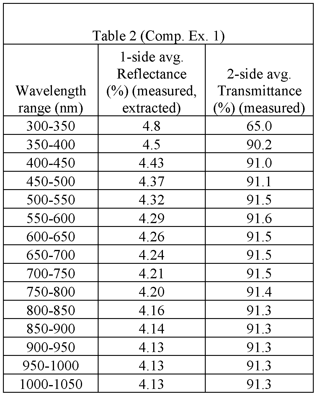

[0183] The first surface reflectance of about 4% is typical of uncoated glass substrates. The substrate of this comparative example is illustrative of a cover glass for a solar panel where the typical porous SiCh antireflective coating has been removed through abrasion, weathering, and cleaning cycles in outdoor service. The transmittance of over 91% in wavelength ranges of from 600 nm to 900 nm illustrates the glass substrate, if allowed not to have an antireflective coating, can reduce substantially the number of usable photons reaching the PV cells. This transmission level is measured for the case where there is an air interface on both of the two surfaces of the glass substrate (there is no polymer bonding layer such as EVA). This is done for ease of measurement at the component level and is consistent with the reported transmittance for all coated examples below. It should be noted that for all coated examples, the coating is applied to only one surface of the glass, meaning that the maximum possible 2- side transmittance values for the 1-side coated glass examples is approximately 96%, due to the approx. 4% reflectance from the uncoated side of the glass.
[0184] Comparative Example 2 - For Comparative Example 2, the same soda lime glass substrate as Comparative Example 1 but this time with a porous SiCE antireflective coating was obtained. Reflectance off the prime surface (“1-side”) of the article as a function of wavelength was measured. In addition, transmittance through the entire article (referred to as “2-side” transmittance) was measured. The measurements were then averaged for various wavelength ranges. The results are set forth in Table 3 below.


[0185] The results reveal that the porous SiCh coating increases the transmittance through the article from just over 91% to within a range of from 94.4% to 94.8% throughout the wavelength range of from 600 nm to 900 nm. As mentioned, the transmittance would decrease during use as a solar panel cover glass as the porous SiCh coating is removed.
[0186] In addition, the nanoindentation hardness of the coated surface of Comparative Example 2 was measured using the Berkovich Indenter Hardness Test and found to be in the range of from 1 to 3 GPa, which corresponds to a relatively low resistance to scratch and abrasion events in our experiments, such as can commonly be encountered by sand particles in solar applications.
[0187] Comparative Example 3 - For Comparative Example 3, an article with a multilayer coating (but not of the present disclosure) was modeled to determine prime surface reflectance and transmittance through the article as in the prior two comparative examples. Comparative Example 3 (and all other modeled Examples herein) were modeled using optical transfer matrix simulations, using input parameters (refractive index and extinction coefficient vs. wavelength) from experimentally fabricated and measured sputtered thin film materials. We have found this modeling approach to yield good agreement with fabricated multilayer film optical properties in numerous prior experiments. The design of the article consisting of a substrate (an alkali aluminosilicate glass composition) and a multilayer coating is as follows in Table 4 below.


[0188] refers to the material (in this case, air) that the model assumes is disposed above the prime surface of the article. Likewise, “emergent” refers to the material (in this case, air) that the model assumes is disposed below the second major surface of the article (provided by the substrate). Layers 1 through 5 refer to the layers of the multilayer coating.
[0189] The model calculated reflectance off the prime surface (“1-side”) of the article as a function of wavelength. In addition, the model calculated transmittance through the entire article (referred to as “2-side” transmittance). The calculations were then averaged for various wavelength ranges. The results are set forth in Table 5 below.


[0190] The multilayer coating of Comparative Example 3 causes greater transmittance through the article throughout the wavelength range of from 450 nm to 600 nm than Comparative Example 2 (porous SiO2 coating). However, the multilayer coating of Comparative Example 3 causes less transmittance through the article throughout the wavelength range of from 600 nm to 1100 nm than Comparative Example 2 (porous SiO2 coating). Comparative Example 3 thus demonstrates that not all multilayer coatings with repeating periods of a layer of low refractive index material and a layer of high refractive index material result in improved antireflective performance compared to the typical porous SiO2 coating.
[0191] Example 1 - For Example 1, an article with a multilayer coating of the present disclosure was modeled as described above to determine prime surface reflectance and transmittance through the article as in the prior two comparative examples. The design of the article consisting of a substrate (a chemically strengthened alkali aluminosilicate glass composition) and a multilayer coating is as follows in Table 6 below.

[0192] The multilayer coating of Example 1 is notable, among other reasons, because (i) the total thickness is within the range of from 350 nm to 1400 nm, (ii) the first layer of low refractive index material (Layer 1) has a thickness within a range of from 50 nm to 250 nm, and (iii) the thicknesses of the layers of low refractive index material combined comprise greater than 55% of the total thickness of the multilayer coating (68.2%). The multilayer
coating of Comparative Example 3 had a thickness (338.4 nm) that is below the former thickness range. Layer 1 of Comparative Example had a thickness (25 nm) that is below the later thickness range. The thicknesses of the layers of low refractive index material combined for Comparative Example 3 was 46.3% of the total thickness of the multilayer coating.
[0193] The model calculated reflectance off the prime surface (“1-side”) of the article as a function of wavelength. In addition, the model calculated transmittance through the entire article (referred to as “2-side” transmittance). The calculations were then averaged for various wavelength ranges. The results are set forth in Table 7 below.

[0194] Unlike the multilayer coating of Comparative Example 3, article with the multilayer coating of Example 1 exhibits lower prime surface reflectance than the porous SiCE coating of Comparative Example 2 throughout entire wavelength range of from 600 nm to 900 nm. The lower reflectance caused the article of Example 1 to exhibit greater transmittance through the
article from 600 nm to 900 nm than the article of Comparative Examples 2 and 3. The prime surface average reflectance throughout the wavelength range of 600 nm to 650 nm that the article of Example 1 exhibits is almost half that which Comparative Example 2 exhibits. Further, the prime surface average reflectance throughout the wavelength range of 300 nm to 350 nm the article of Example 1 exhibits (23.5%) is over 7 times higher than the prime surface average reflectance throughout the same wavelength range that the article of Comparative Example 2 exhibits (3.2%). In addition, the prime surface average reflectance throughout the wavelength range of 1200 nm to 1800 nm the article of Example 1 exhibits (9.8% to 17.9%) is over 5 times to 7 times higher than the prime surface average reflectance throughout the same wavelength range that the article of Comparative Example 2 exhibits (1.7% to 2.5%).
[0195] The graph reproduced at FIG. 10 plots prime surface reflectance as a function of wavelength for Comparative Examples 1-3 and Example 1. The graph reveals that the multilayer coating of Example 1 exhibits lower reflectance than the porous SiO2 coating of Comparative Example 2 throughout key wavelength ranges for solar panel applications (e.g., from 550 nm to about 875 nm). In addition, the graph reveals that the multilayer coating of Example 1 has a much higher reflectance than the porous SiO2 coating of Comparative Example 2 at wavelengths above 1100 nm, which silicon PV cells cannot use.
[0196] The multilayer coating of Example 1 is further notable because the Layer 2 of the high refractive index material (SiNx) has a thickness of 140 nm, which is greater than 80 nm. Further, Layer 2 is within the outermost 300 nm of the total thickness of the multilayer coating. Still further, 52.7% of the outermost 300 nm of the total thickness of the multilayer coating is high refractive index material (SiNx), which is greater than 40%.
[0197] Example 2 - For Example 2, an article with a multilayer coating of the present disclosure was modeled as described above to determine prime surface reflectance and transmittance through the article as in the prior two comparative examples. The design of the article consisting of a substrate (a chemically strengthened alkali aluminosilicate glass composition) and a multilayer coating is as follows in Table 8 below.


[0198] The multilayer coating of Example 2 is notable, among other reasons, because (i) the total thickness is within the range of from 350 nm to 1400 nm (specifically, 1276.9 nm), (ii) the first layer of low refractive index material (Layer 1) has a thickness within a range of from 50 nm to 250 nm (specifically, 206.7 nm), and (iii) the thicknesses of the layers of low refractive index material combined comprise greater than 55% of the total thickness of the multilayer coating (specifically, 59.8%).
[0199] The model calculated reflectance off the prime surface (“1-side”) of the article as a function of wavelength. In addition, the model calculated transmittance through the entire article (referred to as “2-side” transmittance). The calculations were then averaged for various wavelength ranges. The results are set forth in Table 9 below.

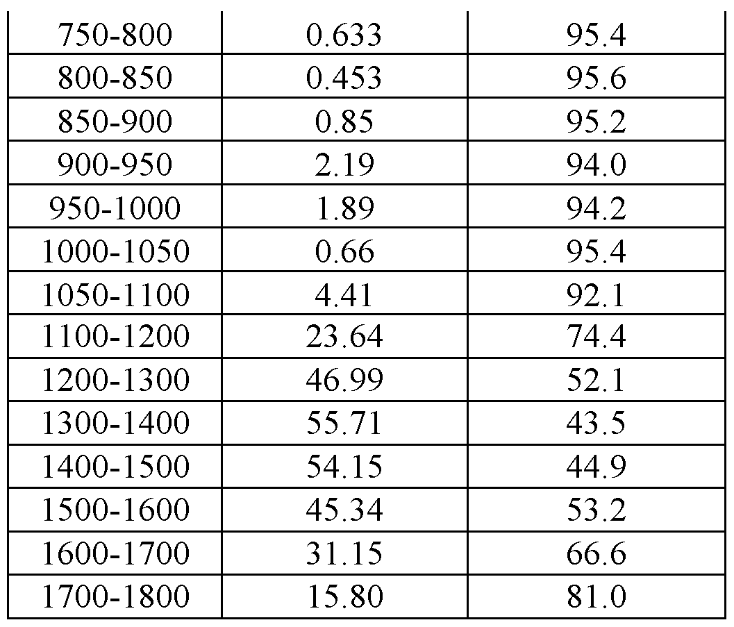
[0200] Unlike the multilayer coating of Comparative Example 3, the article with the multilayer coating of Example 2 exhibits lower prime surface reflectance than the porous SiCE coating of Comparative Example 3 throughout entire wavelength range of from 600 nm to 900 nm, as well as the wavelength range of from 950 nm to 1050 nm. The lower reflectance caused the article of Example 2 to exhibit greater transmittance through the article than the article of Comparative Examples 2 and 3 in these wavelength ranges. The prime surface average reflectance throughout the wavelength range of 800 nm to 850 nm that the article of Example 2 exhibits is almost half that which Comparative Example 2 exhibits. The prime surface average reflectance throughout the wavelength range of 1000 nm to 1050 nm is less than half that which Comparative Example 2 exhibits. Further, the prime surface average reflectance throughout the wavelength range of 300 nm to 350 nm the article of Example 2 exhibits (40.3%) is over 12 times higher than the prime surface average reflectance throughout the same wavelength range that the article of Comparative Example 2 exhibits (3.2%). In addition, the prime surface average reflectance throughout the wavelength range of 1200 nm to 1800 nm the article of Example 2 exhibits (15.8% to 55.7%) is over 9 times to 22 times higher than the prime surface average reflectance throughout the same wavelength range that the article of Comparative Example 2 exhibits (1.7% to 2.5%).
[0201] The graph reproduced at FIG. 11 plots prime surface reflectance as a function of wavelength for Comparative Examples 1 and 2 and Example 2. The graph reveals that the multilayer coating of Example 2 exhibits lower reflectance than the porous SiCh coating of Comparative Example 2 throughout key wavelength ranges for solar panel applications (e.g., from 550 nm to about 875 nm). In addition, the graph reveals that the multilayer coating of
Example 2 has a much higher reflectance than the porous SiO2 coating of Comparative Example 2 at wavelengths above 1100 nm, which silicon PV cells cannot use.
[0202] The multilayer coating of Example 2 is further notable because Layer 2 of the high refractive index material (SiNx) has a thickness of 138.5 nm, which is greater than 80 nm. Further, Layer 2 is within the outermost 300 nm of the total thickness of the multilayer coating. Still further, 51.1% of the outermost 300 nm of the total thickness of the multilayer coating is high refractive index material (SiNx), which is greater than 40%.
[0203] Example 3 - For Example 3, an article with a multilayer coating of the present disclosure was modeled as described above to determine prime surface reflectance and transmittance through the article as in the prior two comparative examples. The design of the article consisting of a substrate (a chemically strengthened alkali aluminosilicate glass composition) and a multilayer coating is as follows in Table 10 below.

[0204] The multilayer coating of Example 3 is notable, among other reasons, because (i) the total thickness is within the range of from 350 nm to 1400 nm (specifically, 544.0 nm), (ii) the first layer of low refractive index material (Layer 1) has a thickness within a range of from 50 nm to 250 nm (specifically, 207.5 nm), and (iii) the thicknesses of the layers of low refractive index material combined comprise greater than 55% of the total thickness of the multilayer coating (specifically, 71.5%).
[0205] The model calculated reflectance off the prime surface (“1-side”) of the article as a function of wavelength. In addition, the model calculated transmittance through the entire
article (referred to as “2-side” transmittance). The calculations were then averaged for various wavelength ranges. The results are set forth in Table 11 below.

[0206] Unlike the multilayer coating of Comparative Example 3, the article with the multilayer coating of Example 3 exhibits lower prime surface reflectance than the porous SiCE coating of Comparative Example 3 throughout entire wavelength range of from 600 nm to 950 nm, as well as the wavelength range of from 1000 nm to 1050 nm. The lower reflectance caused the article of Example 3 to exhibit greater transmittance through the article than the article of Comparative Examples 2 and 3 in these wavelength ranges. The prime surface average reflectance throughout the wavelength range of 800 nm to 900 nm that the article of Example 3 exhibits is almost half that which Comparative Example 2 exhibits. Further, the prime surface average reflectance throughout the wavelength range of 300 nm to 350 nm the article of Example 3 exhibits (28.7%) is almost 9 times higher than the prime surface average reflectance
throughout the same wavelength range that the article of Comparative Example 2 exhibits (3.2%). In addition, the prime surface average reflectance throughout the wavelength range of 1200 nm to 1800 nm the article of Example 3 exhibits (7.1% to 23.5%) is over 4 times to 9 times higher than the prime surface average reflectance throughout the same wavelength range that the article of Comparative Example 2 exhibits (1.7% to 2.5%).
[0207] The multilayer coating of Example 3 is further notable because Layer 4 of the high refractive index material (TiO2) has a thickness of 95.9 nm, which is greater than 80 nm. Further, Layer 4 is within the outermost 300 nm of the total thickness of the multilayer coating. Furthermore, 48.6% of the outermost 300 nm of the total thickness of the multilayer coating is high refractive index material (TiO2), which is greater than 40%.
[0208] Example 4 - For Example 4, an article with a multilayer coating of the present disclosure was modeled as described above to determine prime surface reflectance and transmittance through the article as in the prior two comparative examples. The design of the article consisting of a substrate (this time, a low iron soda-lime glass composition) and a multilayer coating is as follows in Table 12 below.

[0209] The multilayer coating of Example 4 is notable, among other reasons, because (i) the total thickness is within the range of from 350 nm to 1400 nm (specifically, 540.3 nm), (ii) the first layer of low refractive index material (Layer 1) has a thickness within a range of from 50 nm to 250 nm (specifically, 207.0 nm), and (iii) the thicknesses of the layers of low refractive
index material combined comprise greater than 55% of the total thickness of the multilayer coating (specifically, 71.7%).
[0210] The model calculated reflectance off the prime surface (“1-side”) of the article as a function of wavelength. In addition, the model calculated transmittance through the entire article (referred to as “2-side” transmittance). The calculations were then averaged for various wavelength ranges. The results are set forth in Table 13 below.

[0211] Unlike the multilayer coating of Comparative Example 3, the article with the multilayer coating of Example 4 exhibits lower prime surface reflectance than the porous SiCE coating of Comparative Example 3 throughout entire wavelength range of from 600 nm to 1000 nm. The lower reflectance caused the article of Example 4 to exhibit greater transmittance through the article than the article of Comparative Examples 2 and 3 in these wavelength ranges. The prime surface average reflectance throughout the wavelength range of 800 nm to 850 nm that
the article of Example 4 exhibits is almost half that which Comparative Example 2 exhibits. Both Example 3 and Example 4 take advantage of the higher refractive index of TiCL relative to SiNx to achieve lower reflectance than Example 1 in certain wavelength ranges. Further, the prime surface average reflectance throughout the wavelength range of 300 nm to 350 nm the article of Example 4 exhibits (29.9%) is over 9 times higher than the prime surface average reflectance throughout the same wavelength range that the article of Comparative Example 2 exhibits (3.2%). In addition, the prime surface average reflectance throughout the wavelength range of 1200 nm to 1800 nm the article of Example 3 exhibits (7.2% to 23.3%) is over 4 times to 9 times higher than the prime surface average reflectance throughout the same wavelength range that the article of Comparative Example 2 exhibits (1.7% to 2.5%).
[0212] The graph reproduced at FIG. 12 plots prime surface reflectance as a function of wavelength for Comparative Examples 1 and 2 and Examples 3 and 4. The graph reveals that the multilayer coatings of Examples 3 and 4 exhibit lower reflectance than the porous SiCh coating of Comparative Example 2 throughout key wavelength ranges for solar panel applications (e.g., from 550 nm to about 975 nm). In addition, the graph reveals that the multilayer coatings of Examples 3 and 4 have a much higher reflectance than the porous SiCh coating of Comparative Example 2 at wavelengths above 1100 nm, which silicon PV cells cannot use.
[0213] The multilayer coating of Example 4 is further notable because Layer 4 of the high refractive index material (TiCL) has a thickness of 91.3 nm, which is greater than 80 nm. Further, Layer 4 is within the outermost 300 nm of the total thickness of the multilayer coating. Furthermore, 47.7% of the outermost 300 nm of the total thickness of the multilayer coating is high refractive index material (TiCL), which is greater than 40%.
[0214] Hardness Modeling for Comparative Example 3 and Examples 1 through 4 - Hardness was measured experimentally on sputtered single-layer films of SiCL, SiNx, and TiCL, and these measured single-layer hardness values were used as inputs into a finite element model to calculate the hardness of the multilayer coatings Comparative Example 3 and Examples 1 through 4. This combined experiment and modeling approach has been found to agree well in the past with experimentally measured hardness values on full multilayer coating stacks. Finite element modeling of hardness was done using commercial finite element software, ABAQUS v2019. An axisymmetric model was used to reduce the computational time and a conical indenter tip with a semi-angle of 70.3° was assumed, which generates the same contact area- to-depth ratio as the Berkovich diamond indenter. The model includes characteristics of individual layers of the multilayer coating and the substrate. The materials were assumed to
behave in an elastic-perfectly plastic manner, assuming a von Mises yield criterion. Material properties chosen for each individual layer of the multilayer coating were calibrated to known hardness and modulus curves measured for single layer coatings. The outputs of the finite element modeling are load-displacement curves which were then utilized to calculate hardness versus depth curves. To extract hardness as a function of nanoindentation depth, continuous stiffness measurement (CSM) can be simulated. To this end, the modeled indenter tip was given a small amplitude of vibration during the loading stage. For our simulation, displacement history of the tip was prescribed by a user-defined “Amplitude” curve in ABAQUS to impose a very small (~1 nm or less) harmonic unloading. The maximum time increment was limited in such a way that history output can have a high sampling rate to capture all these 1 nm “unloading” portions during the overall loading stage. The hardness responses were then calculated using the Oliver-Pharr method set forth at Oliver, W.C.; Pharr, G.M. An improved technique for determining hardness and elastic modulus using load and displacement sensing indentation experiments. J. Mater. Res. 1992, 7, 1564-1583, and Oliver, W.C.; Pharr, G.M. Measurement of hardness and elastic modulus by instrumented indentation: Advances in understanding and refinements to methodology. J. Mater. Res. 2004, 19, 3-20, both of which are incorporated by reference. The modeled hardness values for Comparative Example 1 and Examples 1 through 4 are shown in Table 13 below. Hardness values are reported at indentation depths of 20 nm, 40 nm, 100 nm, and 125 nm, as well as Hmax which is the maximum hardness at any indentation depth. While Comparative Example 3 has similar hardness to Examples 1 through 4, it does not have the desired spectral characteristics, particularly in the wavelength range of from 600 nm to 800nm, which is important for solar applications. Examples 1 through 4 do have the desired spectral characteristics, together with hardness values that are much higher than the porous SiCE coating of Comparative Example 2, which had measured hardness within a range of from 1 GPa to 3 GPa. Examples 1-4 all have hardness values greater than 7 GPa at all reported depths, greater than 8 GPa at depths of 100 nm or greater, and Hmax values greater than 8 GPa. Due to the higher hardness of the particular sputtered SiNx films used, Examples 1 and Ex. 2 have even higher hardness values, with hardness at 100 nm depth, 125 nm depth, and Hmax values greater than 10 GPa or even greater than 11 GPa. “7/ @ 20 nm” in Table 14 below, for example, means hardness at 20 nm depth.

[0215] Energy Generation Efficiency of Comparative Examples 1 through 3 and Examples 1 through 4 - To assess, from a solar cell or module energy generation efficiency standpoint, the optical performance of the multilayer coatings of the present disclosure, we have calculated the short-circuit current density, Jsc, expected for a standard PV module employing these multilayer coatings. This model takes into account both the spectral composition of sunlight (using the AM 1.5G photon flux, see again FIG. 1) as well as the varying electrical conversion efficiency of the crystalline silicon solar module, with wavelength, considering the effect of each modeled component. The module model is illustrated at FIG. 13. In all cases, the glass substrate, EVA, SiNx, and Si layers have thicknesses of 2.0 mm, 0.5 mm, 76.3 nm, and 300 pm, respectively. It is assumed that the EVA/SiNx/Si thin film interface has a square pyramidal texture. The Si layer consists of an emitter (n-doped Si), space charge region (depletion layer), and base (p-doped Si) with thicknesses of 0.5 pm, 1.0 pm, and 298.5 pm, respectively. The internal quantum efficiency (IQE) of the Si layer is calculated as described in Yang, W. J., et al. (2007), “Internal Quantum Efficiency for Solar Cells,” Solar Energy, 82, 106-110, which is incorporated herein by reference. The Si layer is treated as flat in the IQE calculation with the same parameters as set forth therein, except with an emitter surface recombination velocity of 1E5 cm/s. The total transmittance, T(k), into the Si cell is determined by calculating the losses from reflection and absorption in the various module layers from their complex refractive indices (for normal incidence). In the case of the multilayer coating, the reflectance already computed for each Example is used. The internal absorption of the glass layer is held constant and based on the measured transmittance and absorption of a commercial low-iron soda-lime glass used for PV cover glass applications. The external quantum efficiency (EQE(k)) of the cell is computed as the product: T(k) x IQE(k). The short-circuit current density is then given by the integral from 0 to co, with respect to wavelength, of the product: EQE(k) x AM1.5G photon flux (s'1 m'2 nm'1) x fundamental charge, q (C).
[0216] Table 15 below displays the results of the model. Relative to the module with uncoated substrate (Comparative Example 1), the module with a single porous SiCE coating
(Comparative Example 2) has a 3.31% larger Jsc. To a good approximation, these changes are equivalent to the changes in the efficiency of the module. Example 1 has a similar predicted module efficiency as Comparative Example. 2. However, the multilayer coating of Example 1 has substantially higher hardness and durability than the porous SiCh coating of Comparative Example 2 and imparts greater longevity to the components of the solar panel due to greater reflectance of certain wavelength ranges than the porous SiCh coating of Comparative Example 2. As noted earlier, Comparative. Example 3 has similar hardness to Examples 1 through 4, but its suboptimal spectral characteristics lead to a lower level of solar energy generation, as shown in the Jsc calculation in Table 15. Examples 2 through 4 are predicted to result in a higher Jsc than Comparative Example 2, with increases of 3.64% relative to Comparative Example 1, as well as a substantially higher hardness than Comparative Example 2 and greater reflectance of certain undesirable wavelengths affecting longevity. Therefore, the multilayer coatings of the present disclosure are competitive or advantaged compared to a well-optimized porous SiCh coating used in the PV industry in terms of energy generation efficiency, coating durability, and longevity of components of the solar panel.

[0217] The anti-reflective coatings and articles described in the present disclosure are optimized for use in solar cell and solar panel applications. These applications may include standard utility scale or residential rooftop solar, and may also include recently emerging applications such as solar panels on cars, trucks, or boats (a.k.a. vehicle integrated photovoltaics); opaque, semi-transparent, or transparent solar panels integrated into architectural windows, facades, awnings, and the like (a.k.a. building integrated photovoltaics); parking canopies or parking lot covers; and solar cells integrated into mobile devices such as tablet or laptop computers, external batteries, and smartphones. The anti-reflective coatings and articles of the invention are also
useful in non-solar applications, particularly applications that may benefit from simultaneous visible and near-infrared light transmission, such as display cover glass, camera lens cover glass, information display optics, and sensor cover glass which may be used in smartwatch, smartphone, and augmented reality glasses applications. For example, modern smartphone displays and cameras designed for visible light wavelengths from 400-700 nm may also be integrated with light emitters or sensors operating in the 750-950nm wavelength window, for which the coatings and articles of the present invention are useful.
[0218] Many variations and modifications may be made to the above-described embodiments/aspects of the disclosure without departing substantially from the spirit and various principles of the disclosure. All such modifications and variations are intended to be included herein within the scope of this disclosure and protected by the following claims.
Claims
1. An article comprising: a substrate comprising a first major surface and a second major surface; and a multilayer coating disposed on the first major surface of the substrate, the multilayer coating comprising at least one period of a layer of low refractive index material and a layer of high refractive index material, wherein, the article exhibits a prime surface average reflectance of less than or equal to 0.550% across an entire wavelength range of from 600 nm to 750 nm.
2. The article of claim 1, wherein the substrate further comprises a glass composition or a glass-ceramic composition.
3. The article of claim 2, wherein the glass composition is an alkali aluminosilicate glass composition, a soda lime glass composition, or an alkaline earth boro-aluminosilicate glass composition.
4. The article of any one of claims 1 through 3, wherein the low refractive index material has a refractive index within a range of from 1.40 to 1.60, and the high refractive index material has a refractive index within a range of from 1.70 to 2.50.
5. The article of any one of claims 1 through 4, wherein the low refractive index material is or comprises SiO2, doped SiO2, AI2O3, GeO2, SiO, A10xNy, SiOxNy, SiuAlyOxNy, MgO, MgF2, BaF2, CaF2, DyF3, YbF3, YF3, and CeF3, and the high refractive index material is or comprises AIN, SiNx, A10xNy, SiOxNy, or TiO2.
6. The article of any one of claims 1 through 5, wherein the multilayer coating comprises a first layer of low refractive index material in direct contact with the first major surface, the first layer of low refractive index material having a thickness within a range of from 50 nm to 250 nm.
7. The article of any one of claims 1 through 6, wherein
the multilayer coating further comprises a total thickness that is within a range of from
350 nm to 1400 nm.
8. The article of any one of claims 1 through 6, wherein the multilayer coating further comprises a total thickness that is within a range of from 350 nm to 800 nm.
9. The article of any one of claims 1 through 6, wherein the multilayer coating further comprises a total thickness that is within a range of from 350 nm to 650 nm.
10. The article of any one of claims 7 through 9, wherein thicknesses of the layers of low refractive index material combined comprise greater than 55% of the total thickness of the multilayer coating.
11. The article of claim 10, wherein the thicknesses of the layers of low refractive index material combined comprise within a range of from 65% to 75% of the total thickness of the multilayer coating.
12. The article of any one of claims 1 through 11, wherein the article exhibits a prime surface average reflectance of less than or equal to 2.0% across an entire wavelength range of from 400 nm to 450 nm.
13. The article of any one of claims 1 through 12, wherein the article exhibits a prime surface average reflectance of less than or equal to 1.40% across an entire wavelength range of from 450 nm to 600 nm.
14. The article of any one of claims 1 through 13, wherein the article exhibits a prime surface average reflectance of less than or equal to 0.730% across an entire wavelength range of from 750 nm to 800 nm.
15. The article of any one of claims 1 through 14, wherein the article exhibits a prime surface average reflectance of less than or equal to 0.850% across an entire wavelength range of from 800 nm to 850 nm.
16. The article of any one of claims 1 through 15, wherein the article exhibits a prime surface average reflectance of less than or equal to 1.05% across an entire wavelength range of from 850 nm to 900 nm.
17. The article of any one of claims 1 through 16, wherein the article exhibits a prime surface average reflectance of less than or equal to 2.20% across an entire wavelength range of from 900 nm to 950 nm.
18. The article of any one of claims 1 through 17, wherein the article exhibits a prime surface average reflectance of less than or equal to 3.00% across an entire wavelength range of from 950 nm to 1000 nm.
19. The article of any one of claims 1 through 18, wherein the article exhibits a prime surface average reflectance of less than or equal to 1.40% across an entire wavelength range of from 1000 nm to 1050 nm.
20. The article of any one of claims 1 through 19, wherein the article exhibits a prime surface average reflectance of greater than or equal to 5.0% over one or more of the following wavelength ranges: from 1100 nm to 1200 nm, from 1200 nm to 1300 nm, from 1300 nm to 1400 nm, from 1400 nm to 1500 nm, from 1500 nm to 1600 nm, from 1600 nm to 1700 nm, and from 1700 nm to 1800 nm.
21. The article of any one of claims 1 through 20, wherein the multilayer coating exhibits a maximum hardness of greater than or equal to 6 GPa measured over an indentation depth range from 0 to 125 nm according to a Berkovich Indenter Hardness Test.
22. The article of any one of claims 1 through 20, wherein the multilayer coating exhibits a maximum hardness of greater than or equal to 8 GPa measured over an indentation depth range from 0 to 125 nm according to a Berkovich Indenter Hardness Test.
23. The article of any one of claims 1 through 22 further comprising
an anti-soiling coating upon the multilayer coating, wherein, the anti-soiling coating comprises a silane or a siloxane material, and wherein, the anti-soiling coating exhibits hydrophobic, hydrophilic, or omniphobic properties.
24. The article of any one of claims 1 through 22 further comprising: an anti-soiling coating upon the multilayer coating, wherein, the anti-soiling coating comprises (i) a silicon-containing matrix layer and (ii) a hydrophobic or hydrophilic surface modification material, and wherein, the anti-soiling layer exhibits hydrophobic, hydrophilic, or omniphobic properties.
25. An article comprising: a substrate comprising a first major surface and a second major surface; and a multilayer coating disposed on the first major surface of the substrate, the multilayer coating comprising (i) at least four layers, (ii) repeating periods of a layer of low refractive index material and a layer of high refractive index material, (iii) a total thickness that is within a range of from 350 nm to 1400 nm, (iv) a first layer of low refractive index material disposed directly on the first major surface of substrate, the first layer of low refractive index material comprising a thickness within a range of from 50 nm to 250 nm; wherein, thicknesses of the layers of low refractive index material combined comprise greater than 55% of the total thickness of the multilayer coating.
26. The article of claim 25, wherein the substrate further comprises a glass composition or a glass-ceramic composition.
27. The article of claim 26, wherein the glass composition of the substrate is an alkali aluminosilicate glass composition, a soda lime glass composition, or an alkaline earth boro-aluminosilicate glass composition.
28. The article of any one of claims 25 through 27, wherein the substrate comprises a region of compressive stress at or near the first major surface.
29. The article of any one of claims 25 through 28, wherein
the substrate comprises a thickness within a range of from 0.1 mm to 5.0 mm.
30. The article of any one of claims 25 through 29, wherein the low refractive index material has a refractive index within a range of from 1.40 to 1.60, and the high refractive index material has a refractive index within a range of from 1.70 to 2.50.
31. The article of any one of claims 25 through 30, wherein the low refractive index material is or comprises SiO2, doped SiO2, AI2O3, GeO2, SiO, A10xNy, SiOxNy, SiuAlyOxNy, MgO, MgF2, BaF2, CaF2, DyF3, YbF3, YF3, and CeF3 and the high refractive index material is or comprises AIN, SiNx, A10xNy, SiOxNy, or TiO2.
32. The article of any one of claims 25 through 31, wherein the layers of the low refractive index material comprise from 65% to 75% of the total thickness of the multilayer coating.
33. The article of any one of claims 25 through 32, wherein the multilayer coating comprises a first layer of low refractive index material disposed directly on the first major surface of the substrate, the first layer comprising a thickness within a range of from 175 nm to 225 nm, a second layer of high refractive index material disposed directly on the first layer, the second layer comprising a thickness within a range of from 15 nm to 25 nm, a third layer of low refractive index material disposed directly on the second layer, the third layer comprising a thickness within a range of from 30 nm to 40 nm, a fourth layer of high refractive index material disposed directly on the third layer, the fourth layer comprising a thickness within a range of from 130 nm to 150 nm, and a fifth layer of low refractive index material disposed directly on the fourth layer, the fifth layer comprising a thickness within a range of from 90 nm to 110 nm.
34. The article of any one of claims 25 through 32, wherein the multilayer coating comprises
a first layer of low refractive index material disposed directly on the first major surface of the substrate, the first layer comprising a thickness within a range of from 175 nm to 225 nm, a second layer of high refractive index material disposed directly on the first layer, the second layer comprising a thickness within a range of from 5 nm to 15 nm, a third layer of low refractive index material disposed directly on the second layer, the third layer comprising a thickness within a range of from 35 nm to 60 nm, a fourth layer of high refractive index material disposed directly on the third layer, the fourth layer comprising a thickness within a range of from 20 nm to 30 nm, a fifth layer of low refractive index material disposed directly on the fourth layer, the fifth layer comprising a thickness within a range of from 10 nm to 25 nm, a sixth layer of high refractive index material disposed directly on the fifth layer, the sixth layer comprising a thickness within a range of from 75 nm to 110 nm, a seventh layer of low refractive index material disposed directly on the sixth layer, the seventh layer comprising a thickness within a range of from 5 nm to 20 nm, an eighth layer of high refractive index material disposed directly on the seventh layer, the eighth layer comprising a thickness within a range of from 15 nm to 30 nm, and a ninth layer of low refractive index material disposed directly on the eighth layer, the ninth layer comprising a thickness within a range of from 90 nm to 115 nm.
35. The article of any one of claims 25 through 32, wherein the multilayer coating comprises a first layer of low refractive index material disposed directly on the first major surface of the substrate, the first layer comprising a thickness within a range of from 175 nm to 225 nm, a second layer of high refractive index material disposed directly on the first layer, the second layer comprising a thickness within a range of from 15 nm to 25 nm, a third layer of low refractive index material disposed directly on the second layer, the third layer comprising a thickness within a range of from 30 nm to 40 nm, a fourth layer of high refractive index material disposed directly on the third layer, the fourth layer comprising a thickness within a range of from 130 nm to 160 nm, a fifth layer of low refractive index material disposed directly on the fourth layer, the fifth layer comprising a thickness within a range of from 25 nm to 40 nm,
a sixth layer of high refractive index material disposed directly on the fifth layer, the sixth layer comprising a thickness within a range of from 10 nm to 20 nm, a seventh layer of low refractive index material disposed directly on the sixth layer, the seventh layer comprising a thickness within a range of from 140 nm to 175 nm, an eighth layer of high refractive index material disposed directly on the seventh layer, the eighth layer comprising a thickness within a range of from 10 nm to 20 nm, a ninth layer of low refractive index material disposed directly on the eighth layer, the ninth layer comprising a thickness within a range of from 25 nm to 40 nm, a tenth layer of high refractive index material disposed directly on the ninth layer, the tenth layer comprising a thickness within a range of from 130 nm to 160 nm, an eleventh layer of low refractive index material disposed directly on the tenth layer, the eleventh layer comprising a thickness within a range of from 30 nm to 40 nm, a twelfth layer of high refractive index material disposed directly on the eleventh layer, the twelfth layer comprising a thickness within a range of from 10 nm to 20 nm, a thirteenth layer of low refractive index material disposed directly on the twelfth layer, the thirteenth layer comprising a thickness within a range of from 105 nm to 135 nm, a fourteenth layer of high refractive index material disposed directly on the thirteenth layer, the fourteenth layer comprising a thickness within a range of from 10 nm to 20 nm, a fifteenth layer of low refractive index material disposed directly on the fourteenth layer, the fifteenth layer comprising a thickness within a range of from 35 nm to 50 nm, a sixteenth layer of high refractive index material disposed directly on the fifteenth layer, the sixteenth layer comprising a thickness within a range of from 120 nm to 155 nm, and a seventeenth layer of low refractive index material disposed directly on the sixteenth layer, the seventeenth layer comprising a thickness within a range of from 90 nm to 110 nm.
36. The article of any one of claims 25 through 35, wherein
the article exhibits a prime surface average reflectance of less than or equal to 0.550% across an entire wavelength range of from 600 nm to 750 nm.
37. The article of any one of claims 25 through 36, wherein the article exhibits: a prime surface average reflectance of less than or equal to 2.0% across an entire wavelength range of from 400 nm to 450 nm, a prime surface average reflectance of less than or equal to 1.40% across an entire wavelength range of from 450 nm to 600 nm, a prime surface average reflectance of less than or equal to 0.730% across an entire wavelength range of from 750 nm to 800 nm, a prime surface average reflectance of less than or equal to 0.850% across an entire wavelength range of from 800 nm to 850 nm, a prime surface average reflectance of less than or equal to 1.05% across an entire wavelength range of from 850 nm to 900 nm, a prime surface average reflectance of less than or equal to 2.20% across an entire wavelength range of from 900 nm to 950 nm, a prime surface average reflectance of less than or equal to 3.00% across an entire wavelength range of from 950 nm to 1000 nm, and a prime surface average reflectance of less than or equal to 1.40% across an entire wavelength range of from 1000 nm to 1050 nm.
38. The article of any one of claims 25 through 37, wherein the article exhibits a prime surface average \reflectance of greater than or equal to 5.0% over one or more of the following wavelength ranges: from 1100 nm to 1200 nm, from 1200 nm to 1300 nm, from 1300 nm to 1400 nm, from 1400 nm to 1500 nm, from 1500 nm to 1600 nm, from 1600 nm to 1700 nm, and from 1700 nm to 1800 nm.
39. The article of any one of claims 25 through 38, wherein the multilayer coating exhibits a maximum hardness of greater than or equal to 6 GPa measured over an indentation depth range of from 0 to 125 nm according to a Berkovich Indenter Hardness Test.
40. The article of any one of claims 25 through 38, wherein
the multilayer coating exhibits a maximum hardness of greater than or equal to 8 GPa measured over an indentation depth range of from 0 to 125 nm according to a Berkovich Indenter Hardness Test.
41. The article of any one of claims 25 through 40 further comprising: an anti-soiling coating upon the multilayer coating, wherein, the anti-soiling coating comprises a silane or a siloxane material, and wherein, the anti-soiling coating exhibits hydrophobic, hydrophilic, or omniphobic properties.
42. The article of any one of claims 25 through 40 further comprising: an anti-soiling coating upon the multilayer coating, wherein, the anti-soiling coating comprises (i) a silicon-containing matrix layer and (ii) a hydrophobic or hydrophilic surface modification material, and wherein, the anti-soiling layer exhibits hydrophobic, hydrophilic, or omniphobic properties.
43. A solar panel comprising: an article comprising: a substrate comprising a first major surface and a second major surface; and a multilayer coating disposed on the first major surface of the substrate, the multilayer coating comprising repeating periods of a layer of low refractive index material and a layer of high refractive index material; wherein, the article exhibits a prime surface average reflectance of less than or equal to 0.550% across an entire wavelength range of from 600 nm to 750 nm; and an array of photovoltaic (PV) cells disposed beneath the second major surface of the substrate.
44. The solar panel of claim 43 further comprising: a backsheet, wherein, the array of PV cells is disposed between the backsheet and the article.
45. The solar panel of claim 44 further comprising: a package comprising the article, the array of PV cells, and the backsheet; and
a frame comprising (i) a sidewall extending around a perimeter of the package, (ii) a C- channel contiguous with the sidewall within which the perimeter of the package is secured, and (iii) a tab that extends inward relative to the sidewall and forms a plane that is generally parallel to an outward major surface of the backsheet that faces away from the array of PV cells.
46. The solar panel of any one of claims 43 through 45, wherein the substrate further comprises a glass composition or glass-ceramic composition.
47. The solar panel of claim 46, wherein the glass composition of the substrate is an alkali aluminosilicate glass composition, a soda lime glass composition, or an alkaline earth boro-aluminosilicate glass composition.
48. The solar panel of any one of claims 43 through 47, wherein the low refractive index material has a refractive index within a range of from 1.40 to 1.60, and the high refractive index material has a refractive index within a range of from 1.70 to 2.50.
49. The solar panel of any one of claims 43 through 48, wherein the low refractive index material is or comprises SiO2, doped SiO2, AI2O3, GeO2, SiO, A10xNy, SiOxNy, SiuAlyOxNy, MgO, MgF2, BaF2, CaF2, DyF3, YbF3, YF3, and CeF3 and the high refractive index material is or comprises AIN, SiNx, A10xNy, SiOxNy, or TiO2.
50. The solar panel of any one of claims 43 through 49, wherein the multilayer coating comprises a first layer of low refractive index material in direct contact with the first major surface, the first layer of low refractive index material having a physical thickness in a range of from 50 nm to 250 nm.
51. The solar panel of any one of claims 43 through 50, wherein the multilayer coating further comprises a total thickness that is within a range of from 350 nm to 1400 nm.
52. The solar panel of claim 51, wherein
thicknesses of the layers of low refractive index material combined comprise greater than 55% of the total thickness of the multilayer coating.
53. The solar panel of claim 51, wherein thicknesses of the layers of low refractive index material combined comprise from 65% to 75% of the total thickness of the multilayer coating.
54. The solar panel of any one of claims 43 through 53, wherein the article exhibits a prime surface average reflectance of less than or equal to 2.0% across an entire wavelength range of from 400 nm to 450 nm.
55. The solar panel of any one of claims 43 through 54, wherein the article exhibits a prime surface average reflectance of less than or equal to 1.40% across an entire wavelength range of from 450 nm to 600 nm.
56. The solar panel of any one of claims 43 through 55, wherein the article exhibits a prime surface average reflectance of less than or equal to 0.730% across an entire wavelength range of from 750 nm to 800 nm.
57. The solar panel of any one of claims 43 through 56, wherein the article exhibits a prime surface average reflectance of less than or equal to 0.850% across an entire wavelength range of from 800 nm to 850 nm.
58. The solar panel of any one of claims 43 through 57, wherein the article exhibits a prime surface average reflectance of less than or equal to 1.05% across an entire wavelength range of from 850 nm to 900 nm.
59. The solar panel of any one of claims 43 through 58, wherein the article exhibits a prime surface average reflectance of less than or equal to 2.20% across an entire wavelength range of from 900 nm to 950 nm.
60. The solar panel of any one of claims 43 through 59, wherein the article exhibits a prime surface average reflectance of less than or equal to 3.00% across an entire wavelength range of from 950 nm to 1000 nm.
61. The solar panel of any one of claims 43 through 60, wherein the article exhibits a prime surface average reflectance of less than or equal to 1.40% across an entire wavelength range of from 1000 nm to 1050 nm.
62. The solar panel of any one of claims 43 through 61, wherein the article exhibits a prime surface average reflectance of greater than or equal to 5.0% over one or more of the following wavelength ranges: from 1100 nm to 1200 nm, from 1200 nm to 1300 nm, from 1300 nm to 1400 nm, from 1400 nm to 1500 nm, from 1500 nm to 1600 nm, from 1600 nm to 1700 nm, and from 1700 nm to 1800 nm.
63. The solar panel of any one of claims 43 through 62, wherein the multilayer coating exhibits a maximum hardness of greater than or equal to 6 GPa measured over an indentation depth range from 0 to 125 nm according to a Berkovich Indenter Hardness Test.
64. The solar panel of any one of claims 43 through 63, wherein the multilayer coating exhibits a maximum hardness of greater than or equal to 8 GPa measured over an indentation depth range from 0 to 125 nm according to a Berkovich Indenter Hardness Test.
65. The solar panel of any one of claims 43 through 64, wherein the article further comprises an anti-soiling layer upon the multilayer coating, the anti-soiling coating comprises a silane or a siloxane material, and the anti-soiling coating exhibits hydrophobic, hydrophilic, or omniphobic properties.
66. The solar panel of any one of claims 43 through 64, wherein the article further comprises an anti-soiling coating upon the multilayer coating, the anti-soiling coating comprises (i) a silicon-containing matrix layer and (ii) a hydrophobic or hydrophilic surface modification material, and the anti-soiling layer exhibits hydrophobic, hydrophilic, or omniphobic properties.
67. An article comprising: a substrate comprising a first major surface and a second major surface; and
a multilayer coating disposed on the first major surface of the substrate, the multilayer coating comprising repeating periods of a layer of low refractive index material and a layer of high refractive index material, wherein, the multilayer coating exhibits a maximum hardness of greater than or equal to 6 GPa measured over an indentation depth range from 0 to 125 nm according to a Berkovich Indenter Hardness Test, and wherein, the article exhibits a prime surface average reflectance of less than or equal to 0.900% across an entire wavelength range of from 650 nm to 750 nm.
68. The article of claim 67, wherein the article exhibits: a prime surface average reflectance of less than or equal to 2.50% across an entire wavelength range of from 400 nm to 450 nm, a prime surface average reflectance of less than or equal to 0.650% across an entire wavelength range of from 600 nm to 650 nm, a prime surface average reflectance of less than or equal to 1.00% across an entire wavelength range of from 750 nm to 800 nm, a prime surface average reflectance of less than or equal to 1.00% across an entire wavelength range of from 800 nm to 850 nm, and a prime surface average reflectance of less than or equal to 1.30% across an entire wavelength range of from 850 nm to 900 nm.
69. The article of any one of claims 67 through 68, wherein the article exhibits: a prime surface average reflectance of less than or equal to 2.50% across an entire wavelength range of from 950 nm to 1000 nm, and a prime surface average reflectance of less than or equal to 4.00% across an entire wavelength range of from 1000 nm to 1050 nm.
70. The article of any one of claims 67 through 69, wherein the article exhibits: a prime surface average reflectance of greater than or equal to 17.0% over one or more of the following wavelength ranges: from 1100 nm to 1200 nm, from 1200 nm
to 1300 nm, from 1300 nm to 1400 nm, from 1400 nm to 1500 nm, from 1500 nm to 1600 nm, from 1600 nm to 1700 nm, and from 1700 nm to 1800 nm.
71. The article of any one of claims 67 through 70, wherein the multilayer coating exhibits a maximum hardness of greater than or equal to 8 GPa measured over an indentation depth range from 0 to 125 nm according to a Berkovich Indenter Hardness Test.
72. The article of any one of claims 67 through 71 further comprising: an anti-soiling coating upon the multilayer coating, wherein, the anti-soiling coating comprises a silane or a siloxane material, and wherein, the anti-soiling coating exhibits hydrophobic, hydrophilic, or omniphobic properties.
73. The article of any one of claims 67 through 71 further comprising: an anti-soiling coating upon the multilayer coating, wherein, the anti-soiling coating comprises (i) a silicon-containing matrix layer and (ii) a hydrophobic or hydrophilic surface modification material, and wherein, the anti-soiling layer exhibits hydrophobic, hydrophilic, or omniphobic properties.
Priority Applications (1)
| Application Number | Priority Date | Filing Date | Title |
|---|---|---|---|
| CN202480059305.1A CN121925967A (en) | 2023-08-23 | 2024-08-16 | Article having a substrate and a multilayer coating on the substrate and solar panel comprising said article |
Applications Claiming Priority (2)
| Application Number | Priority Date | Filing Date | Title |
|---|---|---|---|
| US202363534146P | 2023-08-23 | 2023-08-23 | |
| US63/534,146 | 2023-08-23 |
Publications (1)
| Publication Number | Publication Date |
|---|---|
| WO2025042702A1 true WO2025042702A1 (en) | 2025-02-27 |
Family
ID=94732531
Family Applications (1)
| Application Number | Title | Priority Date | Filing Date |
|---|---|---|---|
| PCT/US2024/042603 Pending WO2025042702A1 (en) | 2023-08-23 | 2024-08-16 | Article with a substrate and multilayer coating on the substrate and solar panel incorporating the article |
Country Status (2)
| Country | Link |
|---|---|
| CN (1) | CN121925967A (en) |
| WO (1) | WO2025042702A1 (en) |
Citations (6)
| Publication number | Priority date | Publication date | Assignee | Title |
|---|---|---|---|---|
| US20100215902A1 (en) * | 2009-02-20 | 2010-08-26 | Thorsten Kiehne | White coated polyester film, process for production thereof and use thereof as a backside cover in solar modules |
| US20110232745A1 (en) * | 2010-03-23 | 2011-09-29 | Deposition Sciences, Inc. | Antireflection coating for multi-junction solar cells |
| US20130139868A1 (en) * | 2011-12-06 | 2013-06-06 | Nitto Denko Corporation | Wavelength conversion material as encapsulate for solar module systems to enhance solar harvesting efficiency |
| US20130306127A1 (en) * | 2011-01-28 | 2013-11-21 | Evonik Roehm Gmbh | New solar concentration devices |
| KR20150144279A (en) * | 2014-06-13 | 2015-12-24 | 주식회사 케이씨씨 | Multilayer coated substrate with high reflectance and high durability, useful for rear surface reflection of photovoltaic module and method for manufacturing the same |
| US20230176257A1 (en) * | 2020-09-23 | 2023-06-08 | Leonardo S.P.A. | Multilayer coating for optical solar refector |
-
2024
- 2024-08-16 WO PCT/US2024/042603 patent/WO2025042702A1/en active Pending
- 2024-08-16 CN CN202480059305.1A patent/CN121925967A/en active Pending
Patent Citations (6)
| Publication number | Priority date | Publication date | Assignee | Title |
|---|---|---|---|---|
| US20100215902A1 (en) * | 2009-02-20 | 2010-08-26 | Thorsten Kiehne | White coated polyester film, process for production thereof and use thereof as a backside cover in solar modules |
| US20110232745A1 (en) * | 2010-03-23 | 2011-09-29 | Deposition Sciences, Inc. | Antireflection coating for multi-junction solar cells |
| US20130306127A1 (en) * | 2011-01-28 | 2013-11-21 | Evonik Roehm Gmbh | New solar concentration devices |
| US20130139868A1 (en) * | 2011-12-06 | 2013-06-06 | Nitto Denko Corporation | Wavelength conversion material as encapsulate for solar module systems to enhance solar harvesting efficiency |
| KR20150144279A (en) * | 2014-06-13 | 2015-12-24 | 주식회사 케이씨씨 | Multilayer coated substrate with high reflectance and high durability, useful for rear surface reflection of photovoltaic module and method for manufacturing the same |
| US20230176257A1 (en) * | 2020-09-23 | 2023-06-08 | Leonardo S.P.A. | Multilayer coating for optical solar refector |
Also Published As
| Publication number | Publication date |
|---|---|
| CN121925967A (en) | 2026-04-24 |
Similar Documents
| Publication | Publication Date | Title |
|---|---|---|
| CN103325871B (en) | Cover plate and the photovoltaic module with this cover plate for photovoltaic module | |
| JP5897157B2 (en) | Plate with thermal radiation reflective coating | |
| US20120111400A1 (en) | Optical coating | |
| US20090101209A1 (en) | Method of making an antireflective silica coating, resulting product, and photovoltaic device comprising same | |
| KR101194257B1 (en) | Transparent substrate for solar cell having a broadband anti-reflective multilayered coating thereon and method for preparing the same | |
| US20110111203A1 (en) | Substrate with a sol-gel layer and method for producing a composite material | |
| BRPI0620013A2 (en) | use of a transparent, notably glassy and solar module substrate comprising a plurality of solar cells | |
| AU1941800A (en) | Solar battery module | |
| Agustín-Sáenz et al. | Mechanical properties and field performance of hydrophobic antireflective sol-gel coatings on the cover glass of photovoltaic modules | |
| WO2011026062A2 (en) | Surface nucleated glasses for photovoltaic devices | |
| KR101194258B1 (en) | Transparent substrate for solar cell having a broadband anti-reflective multilayered coating thereon and method for preparing the same | |
| EP2295386B1 (en) | Glass texturing | |
| KR101456220B1 (en) | Transparent substrate having an anti-reflective multilayered coating thereon and method for preparing the same | |
| Chandralekha et al. | Enhanced optical performance of solar cell using hydrophobic SnO2/TEOS/MTMS antireflection coating | |
| CN106291778B (en) | Anti-reflection structure and manufacturing method thereof | |
| WO2025042702A1 (en) | Article with a substrate and multilayer coating on the substrate and solar panel incorporating the article | |
| Chen et al. | A facile strategy to prepare antireflection coatings with high transmittance and improved mechanical stability and application in crystalline silicon solar modules | |
| KR20110120884A (en) | Transparent glass body, method for producing the same, and use thereof | |
| JP2011108753A (en) | Optoelectric transducer and method of manufacturing the same | |
| CN220823659U (en) | Packaging glass for laminated battery assembly | |
| KR101700246B1 (en) | Multilayer coated substrate for rear surface reflection of photovoltaic module and method for manufacturing the same | |
| CN211605166U (en) | A photovoltaic module and photovoltaic power generation system | |
| De et al. | Ordered Mesoporous Slippery Silica Coatings on Photovoltaic Cover Glasses to Enhance Photocurrent with Sustainability for Large-Scale Applications | |
| KR20150002517A (en) | Transparent substrate having an anti-reflective multilayered coating thereon and method for preparing the same | |
| KR20150002516A (en) | Transparent substrate having an anti-reflective multilayered coating thereon and method for preparing the same |
Legal Events
| Date | Code | Title | Description |
|---|---|---|---|
| WWE | Wipo information: entry into national phase |
Ref document number: 2024857067 Country of ref document: EP |