WO2025028301A1 - Etching method and plasma treatment device - Google Patents
Etching method and plasma treatment device Download PDFInfo
- Publication number
- WO2025028301A1 WO2025028301A1 PCT/JP2024/025935 JP2024025935W WO2025028301A1 WO 2025028301 A1 WO2025028301 A1 WO 2025028301A1 JP 2024025935 W JP2024025935 W JP 2024025935W WO 2025028301 A1 WO2025028301 A1 WO 2025028301A1
- Authority
- WO
- WIPO (PCT)
- Prior art keywords
- gas
- substrate
- etching method
- process gas
- plasma
- Prior art date
- Legal status (The legal status is an assumption and is not a legal conclusion. Google has not performed a legal analysis and makes no representation as to the accuracy of the status listed.)
- Pending
Links
Images


Classifications
-
- C—CHEMISTRY; METALLURGY
- C23—COATING METALLIC MATERIAL; COATING MATERIAL WITH METALLIC MATERIAL; CHEMICAL SURFACE TREATMENT; DIFFUSION TREATMENT OF METALLIC MATERIAL; COATING BY VACUUM EVAPORATION, BY SPUTTERING, BY ION IMPLANTATION OR BY CHEMICAL VAPOUR DEPOSITION, IN GENERAL; INHIBITING CORROSION OF METALLIC MATERIAL OR INCRUSTATION IN GENERAL
- C23F—NON-MECHANICAL REMOVAL OF METALLIC MATERIAL FROM SURFACE; INHIBITING CORROSION OF METALLIC MATERIAL OR INCRUSTATION IN GENERAL; MULTI-STEP PROCESSES FOR SURFACE TREATMENT OF METALLIC MATERIAL INVOLVING AT LEAST ONE PROCESS PROVIDED FOR IN CLASS C23 AND AT LEAST ONE PROCESS COVERED BY SUBCLASS C21D OR C22F OR CLASS C25
- C23F4/00—Processes for removing metallic material from surfaces, not provided for in group C23F1/00 or C23F3/00
-
- H—ELECTRICITY
- H10—SEMICONDUCTOR DEVICES; ELECTRIC SOLID-STATE DEVICES NOT OTHERWISE PROVIDED FOR
- H10P—GENERIC PROCESSES OR APPARATUS FOR THE MANUFACTURE OR TREATMENT OF DEVICES COVERED BY CLASS H10
- H10P50/00—Etching of wafers, substrates or parts of devices
- H10P50/20—Dry etching; Plasma etching; Reactive-ion etching
- H10P50/24—Dry etching; Plasma etching; Reactive-ion etching of semiconductor materials
- H10P50/242—Dry etching; Plasma etching; Reactive-ion etching of semiconductor materials of Group IV materials
Definitions
- An exemplary embodiment of the present disclosure relates to an etching method and a plasma processing apparatus.
- Patent Document 1 discloses a method for etching a region made of silicon oxide.
- the method includes a step (a) of exposing a substrate having a region made of silicon oxide to a plasma of a process gas containing a fluorocarbon gas.
- the region is etched and a deposit containing a fluorocarbon is formed on the region.
- the method includes a step (b) of etching the region with fluorocarbon radicals contained in the deposit. Steps (a) and (b) are repeated alternately.
- the present disclosure provides an etching method and plasma processing apparatus that can improve the etching rate.
- the etching method includes the steps of: (a) providing a substrate on a substrate support in a chamber; (b) exposing the substrate to a first process gas comprising hydrogen fluoride gas; and (c) after (b), exposing the substrate to a plasma generated from a second process gas while supplying an electrical bias to the substrate support, the second process gas comprising at least one inert gas selected from the group consisting of noble gases and nitrogen gas.
- an etching method and plasma processing apparatus are provided that can improve the etching rate.
- FIG. 1 is a diagram for explaining an example of the configuration of a plasma processing system.
- FIG. 2 is a diagram for explaining a configuration example of an inductively coupled plasma processing apparatus.
- FIG. 3 is a flow chart of an etching method according to one exemplary embodiment.
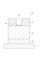
- FIG. 4 is a partial enlarged view of an example substrate to which the method of FIG. 3 may be applied.
- FIG. 5 is a cross-sectional view illustrating a step of an etching method according to an exemplary embodiment.
- FIG. 6 is a cross-sectional view illustrating a step of an etching method according to an exemplary embodiment.
- FIG. 7 is an enlarged partial plan view of an example substrate to which the method of FIG. 3 can be applied.
- FIG. 1 is a diagram for explaining an example of the configuration of a plasma processing system.
- FIG. 2 is a diagram for explaining a configuration example of an inductively coupled plasma processing apparatus.
- FIG. 3 is a flow chart of an etching method according to one
- FIG. 8 is a graph showing an example of the relationship between the number of cycles and the amount of etching.
- FIG. 9 is a graph showing an example of the relationship between the film type and the etching amount.
- FIG. 10 is a flow chart of an etching method according to one exemplary embodiment.
- FIG. 11 is a cross-sectional view illustrating a step of an etching method according to one exemplary embodiment.
- FIG. 12 is a cross-sectional view illustrating a step of an etching method according to one exemplary embodiment.
- FIG. 13 is a cross-sectional view illustrating a step of an etching method according to an exemplary embodiment.
- FIG. 14 is a timing chart showing an example of the change over time in the power and the process gas supplied to the plasma processing apparatus.
- FIG. 1 is a diagram for explaining an example of the configuration of a plasma processing system.
- the plasma processing system includes a plasma processing device 1 and a control unit 2.
- the plasma processing system is an example of a substrate processing system
- the plasma processing device 1 is an example of a substrate processing device.
- the plasma processing device 1 includes a plasma processing chamber 10, a substrate support unit 11, and a plasma generation unit 12.
- the plasma processing chamber 10 has a plasma processing space.
- the plasma processing chamber 10 also has at least one gas supply port for supplying at least one processing gas to the plasma processing space, and at least one gas exhaust port for exhausting gas from the plasma processing space.
- the gas supply port is connected to a gas supply unit 20 described later, and the gas exhaust port is connected to an exhaust system 40 described later.
- the substrate support unit 11 is disposed in the plasma processing space, and has a substrate support surface for supporting a substrate.
- the plasma generating unit 12 is configured to generate plasma from at least one processing gas supplied into the plasma processing space.
- the plasma formed in the plasma processing space may be capacitively coupled plasma (CCP), inductively coupled plasma (ICP), electron-cyclotron-resonance plasma (ECR plasma), helicon wave plasma (HWP), or surface wave plasma (SWP), etc.
- various types of plasma generating units may be used, including AC (Alternating Current) plasma generating units and DC (Direct Current) plasma generating units.
- the AC signal (AC power) used in the AC plasma generating unit has a frequency in the range of 100 kHz to 10 GHz.
- AC signals include RF (Radio Frequency) signals and microwave signals.
- the RF signal has a frequency in the range of 100 kHz to 150 MHz.
- the control unit 2 processes computer-executable instructions that cause the plasma processing apparatus 1 to perform the various steps described in this disclosure.
- the control unit 2 may be configured to control each element of the plasma processing apparatus 1 to perform the various steps described herein. In one embodiment, a part or all of the control unit 2 may be included in the plasma processing apparatus 1.
- the control unit 2 may include a processing unit 2a1, a storage unit 2a2, and a communication interface 2a3.
- the control unit 2 is realized, for example, by a computer 2a.
- the processing unit 2a1 may be configured to perform various control operations by reading a program from the storage unit 2a2 and executing the read program. This program may be stored in the storage unit 2a2 in advance, or may be acquired via a medium when necessary.
- the acquired program is stored in the storage unit 2a2 and is read from the storage unit 2a2 by the processing unit 2a1 and executed.
- the medium may be various storage media readable by the computer 2a, or may be a communication line connected to the communication interface 2a3.
- the processing unit 2a1 may be a CPU (Central Processing Unit).
- the memory unit 2a2 may include a RAM (Random Access Memory), a ROM (Read Only Memory), a HDD (Hard Disk Drive), a SSD (Solid State Drive), or a combination of these.
- the communication interface 2a3 may communicate with the plasma processing device 1 via a communication line such as a LAN (Local Area Network).
- FIG. 1 is a diagram for explaining an example of the configuration of an inductively coupled plasma processing device.
- the inductively coupled plasma processing apparatus 1 includes a plasma processing chamber 10, a gas supply unit 20, a power supply 30, and an exhaust system 40.
- the plasma processing chamber 10 includes a dielectric window 101.
- the plasma processing apparatus 1 also includes a substrate support unit 11, a gas introduction unit, and an antenna 14.
- the substrate support unit 11 is disposed within the plasma processing chamber 10.
- the antenna 14 is disposed on or above the plasma processing chamber 10 (i.e., on or above the dielectric window 101).
- the plasma processing chamber 10 has a plasma processing space 10s defined by the dielectric window 101, a sidewall 102 of the plasma processing chamber 10, and the substrate support unit 11.
- the plasma processing chamber 10 is grounded.
- the substrate support 11 includes a main body 111 and a ring assembly 112.
- the main body 111 has a central region 111a for supporting the substrate W and an annular region 111b for supporting the ring assembly 112.
- a wafer is an example of a substrate W.
- the annular region 111b of the main body 111 surrounds the central region 111a of the main body 111 in a plan view.
- the substrate W is disposed on the central region 111a of the main body 111
- the ring assembly 112 is disposed on the annular region 111b of the main body 111 so as to surround the substrate W on the central region 111a of the main body 111. Therefore, the central region 111a is also called a substrate support surface for supporting the substrate W, and the annular region 111b is also called a ring support surface for supporting the ring assembly 112.
- the main body 111 includes a base 1110 and an electrostatic chuck 1111.
- the base 1110 includes a conductive member.
- the conductive member of the base 1110 may function as a bias electrode.
- the electrostatic chuck 1111 is disposed on the base 1110.
- the electrostatic chuck 1111 includes a ceramic member 1111a and an electrostatic electrode 1111b disposed within the ceramic member 1111a.
- the ceramic member 1111a has a central region 111a. In one embodiment, the ceramic member 1111a also has an annular region 111b. Note that other members surrounding the electrostatic chuck 1111, such as an annular electrostatic chuck or an annular insulating member, may have the annular region 111b.
- the ring assembly 112 may be disposed on the annular electrostatic chuck or the annular insulating member, or may be disposed on both the electrostatic chuck 1111 and the annular insulating member.
- at least one RF/DC electrode coupled to an RF power source 31 and/or a DC power source 32, which will be described later, may be disposed within the ceramic member 1111a.
- the at least one RF/DC electrode functions as a bias electrode.
- the conductive member of the base 1110 and the at least one RF/DC electrode may function as multiple bias electrodes.
- the electrostatic electrode 1111b may function as a bias electrode.
- the substrate support 11 includes at least one bias electrode.
- the ring assembly 112 includes one or more annular members.
- the one or more annular members include one or more edge rings and at least one cover ring.
- the edge rings are formed of a conductive or insulating material, and the cover rings are formed of an insulating material.
- the substrate support 11 may also include a temperature adjustment module configured to adjust at least one of the electrostatic chuck 1111, the ring assembly 112, and the substrate to a target temperature.
- the temperature adjustment module may include a heater, a heat transfer medium, a flow passage 1110a, or a combination thereof.
- a heat transfer fluid such as brine or a gas flows through the flow passage 1110a.
- the flow passage 1110a is formed in the base 1110, and one or more heaters are disposed in the ceramic member 1111a of the electrostatic chuck 1111.
- the substrate support 11 may also include a heat transfer gas supply configured to supply a heat transfer gas to a gap between the back surface of the substrate W and the central region 111a.
- the gas introduction section is configured to introduce at least one processing gas from the gas supply section 20 into the plasma processing space 10s.
- the gas introduction section includes a center gas injector (CGI) 13.
- the center gas injector 13 is disposed above the substrate support section 11 and attached to a central opening formed in the dielectric window 101.
- the center gas injector 13 has at least one gas supply port 13a, at least one gas flow path 13b, and at least one gas inlet port 13c.
- the processing gas supplied to the gas supply port 13a passes through the gas flow path 13b and is introduced into the plasma processing space 10s from the gas inlet port 13c.
- the gas introduction section may include one or more side gas injectors (SGI) attached to one or more openings formed in the sidewall 102.
- SGI side gas injectors
- the gas supply unit 20 may include at least one gas source 21 and at least one flow controller 22.
- the gas supply unit 20 is configured to supply at least one process gas from a corresponding gas source 21 to the gas inlet via a corresponding flow controller 22.
- Each flow controller 22 may include, for example, a mass flow controller or a pressure-controlled flow controller.
- the gas supply unit 20 may include at least one flow modulation device that modulates or pulses the flow rate of the at least one process gas.
- the RF power supply 31 includes a first RF generating unit 31a and a second RF generating unit 31b.
- the first RF generating unit 31a is coupled to the antenna 14 via at least one impedance matching circuit and configured to generate a source RF signal (source RF power) for plasma generation.
- the source RF signal has a frequency in the range of 10 MHz to 150 MHz.
- the first RF generating unit 31a may be configured to generate multiple source RF signals having different frequencies. The generated one or more source RF signals are supplied to the antenna 14.
- the second RF generating unit 31b is coupled to at least one bias electrode via at least one impedance matching circuit and configured to generate a bias RF signal (bias RF power).
- the frequency of the bias RF signal may be the same as or different from the frequency of the source RF signal.
- the bias RF signal has a lower frequency than the frequency of the source RF signal.
- the bias RF signal has a frequency in the range of 100 kHz to 60 MHz.
- the second RF generating unit 31b may be configured to generate multiple bias RF signals having different frequencies.
- the generated one or more bias RF signals are supplied to at least one bias electrode.
- at least one of the source RF signal and the bias RF signal may be pulsed.
- the power supply 30 may also include a DC power supply 32 coupled to the plasma processing chamber 10.
- the DC power supply 32 includes a bias DC generator 32a.
- the bias DC generator 32a is connected to at least one bias electrode and configured to generate a bias DC signal. The generated bias DC signal is applied to the at least one bias electrode.
- the bias DC signal may be pulsed.
- a sequence of voltage pulses is applied to at least one bias electrode.
- the voltage pulses may have a rectangular, trapezoidal, triangular, or combination of these pulse waveforms.
- a waveform generator for generating a sequence of voltage pulses from the DC signal is connected between the bias DC generator 32a and at least one bias electrode.
- the bias DC generator 32a and the waveform generator constitute a voltage pulse generator.
- the voltage pulses may have a positive polarity or a negative polarity.
- the sequence of voltage pulses may include one or more positive voltage pulses and one or more negative voltage pulses within one period.
- the bias DC generator 32a may be provided in addition to the RF power source 31 or may be provided instead of the second RF generator 31b.
- the antenna 14 includes one or more coils.
- the antenna 14 may include an outer coil and an inner coil arranged coaxially.
- the RF power source 31 may be connected to both the outer coil and the inner coil, or to either the outer coil or the inner coil.
- the same RF generator may be connected to both the outer coil and the inner coil, or separate RF generators may be connected separately to the outer coil and the inner coil.
- the exhaust system 40 may be connected to, for example, a gas exhaust port 10e provided at the bottom of the plasma processing chamber 10.
- the exhaust system 40 may include a pressure regulating valve and a vacuum pump. The pressure in the plasma processing space 10s is adjusted by the pressure regulating valve.
- the vacuum pump may include a turbomolecular pump, a dry pump, or a combination thereof.
- FIG. 3 is a flow chart of an etching method according to one exemplary embodiment.
- the etching method MT1 shown in FIG. 3 (hereinafter referred to as "method MT1") can be performed by the plasma processing apparatus 1 of the above embodiment.
- Method MT1 can be applied to the substrate W of FIG. 4.
- the substrate W may include a first region R1 and a second region R2.
- the first region R1 may be a mask.
- the substrate W may not include the first region R1.
- the first region R1 has at least one opening OP.
- the at least one opening OP may be a hole or a slit.
- the first region R1 may have multiple openings OP.
- the second region R2 may be below the first region R1.
- the second region R2 may be a film to be etched.
- the substrate W may further include a base region UR.
- the base region UR may be below the second region R2.
- Each of the first region R1, the second region R2, and the base region UR may be a film.
- the first region R1 includes a first material.
- the first material may include a metal or silicon.
- the metal may be a metal other than tungsten, molybdenum, and titanium.
- the first material may include ruthenium (Ru).
- the second region R2 includes a second material.
- the second material is different from the first material.
- the second material may include at least one selected from the group consisting of silicon, carbon, and metal.
- the second material may be at least one silicon-containing material selected from the group consisting of silicon oxide (SiO x ), silicon nitride (SiN x ), silicon oxynitride (SiON), and polysilicon.
- x is a positive real number.
- the second material may be at least one carbon-containing material selected from the group consisting of photoresist (polymer) and amorphous carbon.
- the second material may include at least one metal selected from the group consisting of tungsten (W), molybdenum (Mo), and titanium (Ti).
- the second material may be a compound including a metal element and a nonmetal element.
- the second material may be at least one selected from the group consisting of metal silicide, metal nitride, and metal carbide.
- the second material may be tungsten silicide (WSi).
- the base region UR includes a third material.
- the third material is different from the first material and the second material.
- the third material may include a metal or silicon.
- Method MT1 will be described below with reference to Figs. 3 to 6, taking as an example a case where method MT1 is applied to a substrate W using the plasma processing apparatus 1 of the above embodiment.
- Figs. 5 to 6 are cross-sectional views showing a step of an etching method according to one exemplary embodiment.
- method MT1 can be performed in the plasma processing apparatus 1 by controlling each part of the plasma processing apparatus 1 by the control unit 2.
- a substrate W on a substrate support 11 arranged in a plasma processing chamber 10 is processed, as shown in Fig. 2.
- Step ST1 a substrate W shown in FIG. 4 is provided on a substrate support 11 in a plasma processing chamber 10.
- Step ST2 the substrate W is exposed to a first processing gas containing hydrogen fluoride (HF) gas.
- HF hydrogen fluoride
- plasma may not be generated from the first processing gas.
- the supply of the first processing gas may be stopped at the end of step ST2.
- step ST2 as shown in FIG. 5, hydrogen fluoride molecules are adsorbed on the surface of the substrate W to form an adsorption layer AB.
- the adsorption layer AB may contain hydrogen fluoride.
- the hydrogen fluoride molecules are adsorbed on the surface of the second region R2.
- the hydrogen fluoride molecules may or may not be adsorbed on the surface of the first region R1.
- the adsorption layer AB may be a layer formed by a reaction between hydrogen fluoride and the second region R2.
- the thickness of the adsorption layer AB may increase over time and may saturate at a certain value.
- the first process gas may further include at least one inert gas selected from the group consisting of noble gases and nitrogen (N 2 ) gas.
- noble gases include argon (Ar) gas, helium (He) gas, xenon (Xe) gas, and neon (Ne) gas.
- the flow rate of hydrogen fluoride gas may be the largest.
- the inert gas that may be contained in the first process gas may be the same as or different from the inert gas contained in the second process gas in step ST4.
- the first process gas may not include a fluorine-containing gas other than hydrogen fluoride gas.
- the duration of step ST2 may be 0.1 to 100 seconds, or 30 to 80 seconds.
- the temperature of the substrate support 11 may be controlled in the range of -10°C to 80°C, or in the range of 10°C to 80°C. In such a range, the adsorption of hydrogen fluoride to silicon oxide is not promoted. Therefore, in step ST4, the etching rate of silicon oxide is smaller than the etching rate of silicon nitride.
- the pressure in the plasma processing chamber 10 may be 100 mTorr (13 Pa) or more. Also, the pressure in the plasma processing chamber 10 may be 1000 mTorr (130 Pa) or less.
- Step ST2 may be performed as follows: A first processing gas is supplied into the plasma processing chamber 10 by the gas supply unit 20.
- the control unit 2 controls the gas supply unit 20 and the plasma generation unit 12 so that plasma is not generated.
- Step ST3 the internal space of the plasma processing chamber 10 is purged.
- the purging may be performed by supplying an inert gas into the plasma processing chamber 10, or by evacuating the internal space of the plasma processing chamber 10.
- the purging may be performed by combining the supply of the inert gas and the evacuation.
- Step ST4 In step ST4, as shown in Fig. 6, while supplying an electric bias to the substrate support 11, the substrate W is exposed to a plasma PL generated from a second processing gas.
- the second processing gas may be different from the first processing gas in step ST2.
- the second processing gas includes at least one inert gas selected from the group consisting of a noble gas and nitrogen ( N2 ) gas.
- the flow rate of the inert gas may be the largest among all the flow rates of the gases included in the second processing gas.
- the second processing gas may not include a halogen gas.
- an electrical bias causes ions IN in the plasma PL to collide with the adsorption layer AB.
- the ions IN may be ions of an inert gas.
- the collision energy of the ions IN causes a reaction between the adsorption layer AB and the substrate W (second region R2), thereby etching the substrate W (second region R2).
- a recess RS is formed in the substrate W (second region R2).
- the etching may be stopped by depletion of the adsorption layer AB.
- the supply of the second process gas may be stopped at the end of step ST4.
- the duration of step ST4 may be shorter than the duration of step ST2.
- the duration of step ST4 may be 1/3 or less of the duration of step ST2.
- the duration of step ST4 may be 0.1 to 100 seconds, or 0.1 to 20 seconds. Since the ions IN are collided with the substrate W (second region R2) by the electrical bias, a large collision energy of the ions IN is imparted to the substrate W (second region R2). Therefore, even if the duration of step ST4 is shortened, a high etching rate can be obtained.
- the temperature of the substrate support 11 may be controlled in the range of -10°C to 80°C, or in the range of 10°C to 80°C.
- the pressure in the plasma processing chamber 10 in step ST4 may be lower than the pressure in the plasma processing chamber 10 in step ST2.
- the pressure in the plasma processing chamber 10 may be 10 mTorr (1.3 Pa) or more.
- the pressure in the plasma processing chamber 10 may be 100 mTorr (13 Pa) or less.
- Step ST4 may be performed as follows. First, the gas supply unit 20 supplies the second processing gas into the plasma processing chamber 10. Next, the plasma generation unit 12 generates plasma PL from the second processing gas in the plasma processing chamber 10. The control unit 2 controls the gas supply unit 20 and the plasma generation unit 12 so that the plasma PL is generated. The control unit 2 controls the power supply 30 so that an electrical bias is supplied to the substrate support unit 11.
- Step ST5 steps ST2 to ST4 are repeated. This allows the etching amount of the second region R2 to be increased, and therefore the recess RS can be deepened.
- an adsorption layer AB may be formed on the sidewall and bottom of the recess RS.
- step ST4 of step ST5 ions IN collide with the adsorption layer AB on the bottom of the recess RS, but are unlikely to collide with the adsorption layer AB on the sidewall of the recess RS.
- the method MT1 described above can improve the etching rate of the substrate W (second region R2) in step ST4.
- the mechanism is presumed to be as follows, but is not limited to this.
- step ST2 hydrogen fluoride molecules are adsorbed onto the surface of the substrate W to form an adsorption layer AB.
- the adsorption layer AB may be a layer formed by the reaction of hydrogen fluoride with the substrate W (second region R2).
- ions IN in the plasma PL collide with the adsorption layer AB due to an electrical bias.
- the collision energy of the ions IN causes the adsorption layer AB to react with the substrate W (second region R2), thereby etching the substrate W (second region R2).
- step ST2 no film is formed by plasma CVD in step ST2. Therefore, the effect of loading on the dimensions (CD: Critical Dimension) and depth of the recess RS can be reduced. Also, the in-plane uniformity of the dimensions (CD) and depth of the recess RS can be improved.
- FIG. 7 is a partially enlarged plan view of an example substrate W to which method MT1 can be applied.
- FIG. 7 shows an XYZ Cartesian coordinate system.
- a first direction X and a second direction Y are directions along the main surface of the substrate W.
- a third direction Z is a direction perpendicular to the main surface of the substrate W.
- the substrate W shown in FIG. 7 includes a second region R2 as a film to be etched.
- the second region R2 has at least one recess RS.
- the recess RS corresponds to the opening OP in the first region R1.
- the recess RS may be formed by etching the second region R2 through the opening OP before step ST2.
- the recess RS has a first pair of side walls SW1 that face each other with a first width XCD in the first direction X, and a second pair of side walls SW2 that face each other with a second width YCD in the second direction Y.
- the second direction Y is perpendicular to the first direction X.
- the second width YCD is greater than the first width XCD.
- the recess RS may have, for example, an elliptical shape in the XY plane that includes the first direction X and the second direction Y.
- an adsorption layer AB is formed in the recess RS.
- the adsorption layer AB may be formed on the sidewalls and bottom of the recess RS.
- the adsorption layer AB may be formed on the first sidewall pair SW1 and the second sidewall pair SW2.
- step ST4 the first sidewall pair SW1 and the second sidewall pair SW2 are etched.
- the recess RS expands in the XY plane including the first direction X and the second direction Y (see the recess RS indicated by the dashed line in FIG. 7).
- the etching amount YEA of each of the second sidewall pair SW2 is greater than the etching amount XEA of each of the first sidewall pair SW1. This is believed to be because the flux of ions IN incident on each of the second sidewall pair SW2 is greater than the flux of ions IN incident on each of the first sidewall pair SW1.
- a substrate was provided on a substrate support in a chamber of a plasma processing apparatus (step ST1).
- the substrate had a SiO 2 film on its surface.
- a first processing gas containing HF gas and Ar gas was supplied onto the substrate without generating plasma (step ST2).
- the duration of step ST2 was 60 seconds.
- argon gas was supplied into the chamber to purge the internal space of the chamber (step ST3).
- the duration of step ST3 was 30 seconds.
- plasma generated from Ar gas was supplied to the substrate while supplying an electric bias to the substrate support (step ST4).
- the duration of step ST4 was 10 seconds.
- steps ST2 to ST4 were repeated so that each of steps ST2 to ST4 was performed three times (cycle number) (step ST5).
- the temperature of the substrate support in steps ST2 to ST5 was ⁇ 5° C.
- Example 8 The eighth experiment was carried out in the same manner as the seventh experiment, except that step ST5 was carried out so that the number of cycles was 20.
- the ninth experiment was carried out in the same manner as the second experiment, except that the substrate had a polysilicon film instead of a SiO2 film.
- the number of cycles was 10.
- Example 16 The 16th experiment was performed in the same manner as the 2nd experiment, except that CF4 gas was used instead of HF gas in the process ST2.
- the substrate has a SiO2 film.
- Example 17 The 17th experiment was carried out in the same manner as the 5th experiment, except that CF4 gas was used instead of HF gas in the step ST2.
- the substrate had a SiN film.
- step ST4 (Duration of step ST4) Except for changing the duration of step ST4 to 2 seconds, 5 seconds, and 20 seconds, etching was performed in the same manner as in the second experiment or the fifth experiment, and the etching amount of the film included in the substrate was measured. As a result, the etching amount increased as the duration of step ST4 increased until the duration of step ST4 was 10 seconds. When the duration of step ST4 was longer than 10 seconds, the etching amount hardly changed even if the duration of step ST4 was longer. This indicates that etching automatically stops when the adsorption layer or reaction layer of HF gas is exhausted.
- FIG. 10 is a flowchart of an etching method according to one exemplary embodiment.
- the etching method MT2 shown in FIG. 10 (hereinafter referred to as "method MT2") can be performed by the plasma processing apparatus 1 of the above embodiment.
- Method MT2 can be applied to the substrate W of FIG. 4.
- method MT2 may include steps ST1, ST21, ST41, and ST5. Steps ST1, ST21, ST41, and ST5 may be performed in sequence. Method MT2 may not include step ST5.
- Step ST1 the substrate W shown in FIG. 4 is provided on the substrate support 11 in the plasma processing chamber 10. Then, as shown in FIG. 11, the second region R2 is etched through the opening OP of the first region R1 by the plasma PL1 generated from the processing gas. As a result, the substrate W including the second region R2 having at least one recess RS is provided on the substrate support 11.
- the recess RS may have a first portion RS1 and a second portion RS2 on the first portion RS1.
- the first portion RS1 may have a first sidewall SW11.
- the first portion RS1 may have a bottom of the recess RS.
- the second portion RS2 may have a second sidewall SW12.
- a protective film PF may be formed on the second sidewall SW12.
- the protective film PF may be formed on the first region R1.
- the protective film PF may be formed simultaneously with the recess RS, or may be formed after the recess RS is formed.
- the protective film PF contains carbon and fluorine.
- the protective film PF may be formed without forming the protective film PF.
- the protective film PF may be formed by, for example, ALD or CVD.
- Step ST21 may be performed in the same manner as step ST2 of method MT1.
- the second region R2 is exposed to a third process gas containing hydrogen fluoride gas while supplying no electric bias or a first level electric bias to the substrate support 11.
- the third process gas may be the same as the process gas used in step ST1.
- the third process gas may further contain a fluorocarbon gas or a hydrofluorocarbon gas.
- plasma may not be generated from the third process gas.
- the surface of the first sidewall SW11 may be modified. As a result, a modified layer MR is formed on the surface of the first sidewall SW11.
- the modified layer MR is not formed on the portion of the surface of the second sidewall SW12 that is covered by the protective film PF.
- the modified layer MR may be an adsorption layer AB shown in FIG. 5.
- Step ST41 may be performed in the same manner as step ST4 of method MT1.
- step ST41 as shown in FIG. 13, while supplying a second level of electric bias to the substrate support 11, the second region R2 is exposed to a plasma PL generated from a fourth process gas including hydrogen fluoride gas.
- the fourth process gas may be the same as the third process gas.
- the fourth process gas may further include a fluorocarbon gas or a hydrofluorocarbon gas.
- the second level of the electric bias supplied to the substrate support 11 in step S41 is greater than the first level of the electric bias that may be supplied to the substrate support 11 in step ST21.
- step ST41 as shown in FIG. 13, the surface (modified layer MR) of the first side wall SW11 modified in step ST21 may be removed. This causes the first side wall SW11 to be etched.
- Step ST5 In the process ST5, a cycle including the process ST21 and the process ST41 is repeated. Each cycle may further include an etching process included in the process ST1 before the process ST21.
- step ST21 a modified layer MR can be formed in the first portion RS1 close to the bottom of the recess RS.
- step ST41 etching of the first portion RS1 close to the bottom of the recess RS can be promoted. This makes it possible to improve the etching rate of the recess RS having a high aspect ratio.
- step ST41 since the first sidewall SW11 can be etched, the dimension (CD) of the recess RS at the bottom of the recess RS can be increased.
- FIG. 14 is a timing chart showing an example of the change over time in the power and process gas supplied to the plasma processing apparatus. This timing chart relates to steps ST1, ST21, ST41, and ST5.
- the plasma processing apparatus 1 may be supplied with source power and bias power.
- the source power may be high frequency power HF applied to the counter electrode (upper electrode).
- the bias power may be high frequency power LF or DC bias applied to an electrode in the main body 111 of the substrate support 11.
- the source power and the bias power may be applied periodically with a period CY.
- the period CY may include a first period PA, a second period PB, and a third period PC.
- the second period PB is the period after the first period PA.
- the third period PC is the period after the second period PB.
- the first period PA and the second period PB in the first period CY correspond to the etching process included in the process ST1.
- a recess RS may be formed as shown in FIG. 11.
- the third period PC corresponds to the process ST21.
- a modified layer MR may be formed as shown in FIG. 12.
- the first period PA and the second period PB after the third period PC correspond to the process ST41.
- the first side wall SW11 may be etched as shown in FIG. 13.
- the third period PC and the subsequent period in the second period CY correspond to the process ST5.
- the power level of the source power may be maintained at level H2, and the power level of the bias power may be maintained at level H1.
- Level H1 is lower than level H2.
- the power level of the source power may be maintained at level L2, and the power level of the bias power may be maintained at level H1.
- Level L2 is lower than level H2.
- Level L2 may be 0 W.
- the power level of the source power may be maintained at level L2, and the power level of the bias power may be maintained at level L1.
- Level L1 is lower than level H1.
- Level L1 may be 0 W.
- a DC bias may be supplied to the substrate support 11 as the electric bias instead of the high frequency power LF.
- the DC bias may include a voltage pulse. If the electric bias is bias RF power, the level of the electric bias is the power level (effective value) of the bias RF power. If the electric bias includes a voltage pulse, the level of the electric bias is the absolute value of the negative voltage level of the voltage pulse.
- the processing gas supplied to the plasma processing apparatus may be supplied continuously over all cycles CY.
- the processing gas may include a fluorocarbon gas, a hydrofluorocarbon gas, and a hydrogen fluoride gas.
- the etching method [E1] described above can improve the etching rate of the substrate in (c).
- (b) can prevent the opening from becoming blocked.
- the substrate includes a film to be etched having at least one recess;
- the at least one recess has a first pair of opposing sidewalls with a first width in a first direction, and a second pair of opposing sidewalls with a second width larger than the first width in a second direction perpendicular to the first direction,
- the etching method according to any one of [E1] to [E13], wherein in (c), the first sidewall pair and the second sidewall pair are etched, and an etching amount of the second sidewall pair is greater than an etching amount of the first sidewall pair.
- [E15] (a) providing a substrate on a substrate support in a chamber, the substrate including a film to be etched having at least one recess; (b) exposing the film to be etched to a third process gas comprising hydrogen fluoride gas while applying no electrical bias or a first level of electrical bias to the substrate support; (c) after (b), exposing the film to be etched to a plasma generated from a fourth process gas including hydrogen fluoride gas while supplying an electric bias of a second level to the substrate support, the second level being greater than the first level;
- the etching method includes:
- the recess has a first portion and a second portion on the first portion, the first portion having a first sidewall and the second portion having a second sidewall; (b) includes modifying a surface of the first sidewall; The etching method according to any one of [E15] to [E17], wherein the step (c) includes removing the surface of the modified first sidewall.
- a chamber a substrate support for supporting a substrate within the chamber; a gas supply configured to supply a first process gas and a second process gas into the chamber, the first process gas comprising hydrogen fluoride gas and the second process gas comprising at least one inert gas selected from the group consisting of a noble gas and a nitrogen gas; a plasma generating unit configured to generate a plasma from the second process gas in the chamber; a power supply for providing an electrical bias to the substrate support;
- a control unit Equipped with The control unit is (b) exposing the substrate to the first process gas; (c) after (b), exposing the substrate to the plasma generated from the second process gas while supplying the electrical bias to the substrate support;
- the plasma processing apparatus is configured to control the gas supply unit, the plasma generation unit, and the power supply so as to perform the above.
- 1...plasma processing device 2...control unit, 10...plasma processing chamber, 11...substrate support unit, 12...plasma generation unit, 20...gas supply unit, 30...power supply, PL...plasma, R2...second region (film to be etched), RS...recess, W...substrate.
Landscapes
- Chemical & Material Sciences (AREA)
- Engineering & Computer Science (AREA)
- Materials Engineering (AREA)
- Mechanical Engineering (AREA)
- Metallurgy (AREA)
- Organic Chemistry (AREA)
- Drying Of Semiconductors (AREA)
- Physics & Mathematics (AREA)
- Plasma & Fusion (AREA)
- Analytical Chemistry (AREA)
Abstract
Description
本開示の例示的実施形態は、エッチング方法及びプラズマ処理装置に関するものである。 An exemplary embodiment of the present disclosure relates to an etching method and a plasma processing apparatus.
特許文献1は、酸化シリコンから構成された領域をエッチングする方法を開示する。この方法は、酸化シリコンから構成された領域を有する基板をフルオロカーボンガスを含む処理ガスのプラズマに晒す工程(a)を含む。工程(a)では、該領域をエッチングし、且つ該領域上にフルオロカーボンを含む堆積物を形成する。この方法は、堆積物に含まれるフルオロカーボンのラジカルにより領域をエッチングする工程(b)を含む。工程(a)と工程(b)とは交互に繰り返される。
本開示は、エッチングレートを向上できるエッチング方法及びプラズマ処理装置を提供する。 The present disclosure provides an etching method and plasma processing apparatus that can improve the etching rate.
一つの例示的実施形態において、エッチング方法は、(a)チャンバ内で基板支持部上に基板を提供する工程と、(b)前記基板を、フッ化水素ガスを含む第1処理ガスに晒す工程と、(c)前記(b)の後、前記基板支持部に電気バイアスを供給しながら、前記基板を、第2処理ガスから生成されるプラズマに晒す工程であり、前記第2処理ガスは、貴ガス及び窒素ガスからなる群から選択される少なくとも1つの不活性ガスを含む、工程と、を含む。 In one exemplary embodiment, the etching method includes the steps of: (a) providing a substrate on a substrate support in a chamber; (b) exposing the substrate to a first process gas comprising hydrogen fluoride gas; and (c) after (b), exposing the substrate to a plasma generated from a second process gas while supplying an electrical bias to the substrate support, the second process gas comprising at least one inert gas selected from the group consisting of noble gases and nitrogen gas.
一つの例示的実施形態によれば、エッチングレートを向上できるエッチング方法及びプラズマ処理装置が提供される。 According to one exemplary embodiment, an etching method and plasma processing apparatus are provided that can improve the etching rate.
以下、図面を参照して種々の例示的実施形態について詳細を説明する。なお、各図面において同一又は相当の部分に対しては同一の符号を附すこととする。 Various exemplary embodiments will be described in detail below with reference to the drawings. Note that the same reference numerals will be used to denote the same or equivalent parts in each drawing.
図1は、プラズマ処理システムの構成例を説明するための図である。一実施形態において、プラズマ処理システムは、プラズマ処理装置1及び制御部2を含む。プラズマ処理システムは、基板処理システムの一例であり、プラズマ処理装置1は、基板処理装置の一例である。プラズマ処理装置1は、プラズマ処理チャンバ10、基板支持部11及びプラズマ生成部12を含む。プラズマ処理チャンバ10は、プラズマ処理空間を有する。また、プラズマ処理チャンバ10は、少なくとも1つの処理ガスをプラズマ処理空間に供給するための少なくとも1つのガス供給口と、プラズマ処理空間からガスを排出するための少なくとも1つのガス排出口とを有する。ガス供給口は、後述するガス供給部20に接続され、ガス排出口は、後述する排気システム40に接続される。基板支持部11は、プラズマ処理空間内に配置され、基板を支持するための基板支持面を有する。
FIG. 1 is a diagram for explaining an example of the configuration of a plasma processing system. In one embodiment, the plasma processing system includes a
プラズマ生成部12は、プラズマ処理空間内に供給された少なくとも1つの処理ガスからプラズマを生成するように構成される。プラズマ処理空間において形成されるプラズマは、容量結合プラズマ(CCP;Capacitively Coupled Plasma)、誘導結合プラズマ(ICP;Inductively Coupled Plasma)、ECRプラズマ(Electron-Cyclotron-resonance plasma)、ヘリコン波励起プラズマ(HWP:Helicon Wave Plasma)、又は、表面波プラズマ(SWP:Surface Wave Plasma)等であってもよい。また、AC(Alternating Current)プラズマ生成部及びDC(Direct Current)プラズマ生成部を含む、種々のタイプのプラズマ生成部が用いられてもよい。一実施形態において、ACプラズマ生成部で用いられるAC信号(AC電力)は、100kHz~10GHzの範囲内の周波数を有する。従って、AC信号は、RF(Radio Frequency)信号及びマイクロ波信号を含む。一実施形態において、RF信号は、100kHz~150MHzの範囲内の周波数を有する。
The
制御部2は、本開示において述べられる種々の工程をプラズマ処理装置1に実行させるコンピュータ実行可能な命令を処理する。制御部2は、ここで述べられる種々の工程を実行するようにプラズマ処理装置1の各要素を制御するように構成され得る。一実施形態において、制御部2の一部又は全てがプラズマ処理装置1に含まれてもよい。制御部2は、処理部2a1、記憶部2a2及び通信インターフェース2a3を含んでもよい。制御部2は、例えばコンピュータ2aにより実現される。処理部2a1は、記憶部2a2からプログラムを読み出し、読み出されたプログラムを実行することにより種々の制御動作を行うように構成され得る。このプログラムは、予め記憶部2a2に格納されていてもよく、必要なときに、媒体を介して取得されてもよい。取得されたプログラムは、記憶部2a2に格納され、処理部2a1によって記憶部2a2から読み出されて実行される。媒体は、コンピュータ2aに読み取り可能な種々の記憶媒体であってもよく、通信インターフェース2a3に接続されている通信回線であってもよい。処理部2a1は、CPU(Central Processing Unit)であってもよい。記憶部2a2は、RAM(Random Access Memory)、ROM(Read Only Memory)、HDD(Hard Disk Drive)、SSD(Solid State Drive)、又はこれらの組み合わせを含んでもよい。通信インターフェース2a3は、LAN(Local Area Network)等の通信回線を介してプラズマ処理装置1との間で通信してもよい。
The control unit 2 processes computer-executable instructions that cause the
以下に、プラズマ処理装置1の一例としての誘導結合型のプラズマ処理装置の構成例について説明する。図2は、誘導結合型のプラズマ処理装置の構成例を説明するための図である。
Below, we will explain an example of the configuration of an inductively coupled plasma processing device as an example of the
誘導結合型のプラズマ処理装置1は、プラズマ処理チャンバ10、ガス供給部20、電源30及び排気システム40を含む。プラズマ処理チャンバ10は、誘電体窓101を含む。また、プラズマ処理装置1は、基板支持部11、ガス導入部及びアンテナ14を含む。基板支持部11は、プラズマ処理チャンバ10内に配置される。アンテナ14は、プラズマ処理チャンバ10上又はその上方(すなわち誘電体窓101上又はその上方)に配置される。プラズマ処理チャンバ10は、誘電体窓101、プラズマ処理チャンバ10の側壁102及び基板支持部11により規定されたプラズマ処理空間10sを有する。プラズマ処理チャンバ10は接地される。
The inductively coupled
基板支持部11は、本体部111及びリングアセンブリ112を含む。本体部111は、基板Wを支持するための中央領域111aと、リングアセンブリ112を支持するための環状領域111bとを有する。ウェハは基板Wの一例である。本体部111の環状領域111bは、平面視で本体部111の中央領域111aを囲んでいる。基板Wは、本体部111の中央領域111a上に配置され、リングアセンブリ112は、本体部111の中央領域111a上の基板Wを囲むように本体部111の環状領域111b上に配置される。従って、中央領域111aは、基板Wを支持するための基板支持面とも呼ばれ、環状領域111bは、リングアセンブリ112を支持するためのリング支持面とも呼ばれる。
The
一実施形態において、本体部111は、基台1110及び静電チャック1111を含む。基台1110は、導電性部材を含む。基台1110の導電性部材はバイアス電極として機能し得る。静電チャック1111は、基台1110の上に配置される。静電チャック1111は、セラミック部材1111aとセラミック部材1111a内に配置される静電電極1111bとを含む。セラミック部材1111aは、中央領域111aを有する。一実施形態において、セラミック部材1111aは、環状領域111bも有する。なお、環状静電チャックや環状絶縁部材のような、静電チャック1111を囲む他の部材が環状領域111bを有してもよい。この場合、リングアセンブリ112は、環状静電チャック又は環状絶縁部材の上に配置されてもよく、静電チャック1111と環状絶縁部材の両方の上に配置されてもよい。また、後述するRF電源31及び/又はDC電源32に結合される少なくとも1つのRF/DC電極がセラミック部材1111a内に配置されてもよい。この場合、少なくとも1つのRF/DC電極がバイアス電極として機能する。なお、基台1110の導電性部材と少なくとも1つのRF/DC電極とが複数のバイアス電極として機能してもよい。また、静電電極1111bがバイアス電極として機能してもよい。従って、基板支持部11は、少なくとも1つのバイアス電極を含む。
In one embodiment, the
リングアセンブリ112は、1又は複数の環状部材を含む。一実施形態において、1又は複数の環状部材は、1又は複数のエッジリングと少なくとも1つのカバーリングとを含む。エッジリングは、導電性材料又は絶縁材料で形成され、カバーリングは、絶縁材料で形成される。
The
また、基板支持部11は、静電チャック1111、リングアセンブリ112及び基板のうち少なくとも1つをターゲット温度に調節するように構成される温調モジュールを含んでもよい。温調モジュールは、ヒータ、伝熱媒体、流路1110a、又はこれらの組み合わせを含んでもよい。流路1110aには、ブラインやガスのような伝熱流体が流れる。一実施形態において、流路1110aが基台1110内に形成され、1又は複数のヒータが静電チャック1111のセラミック部材1111a内に配置される。また、基板支持部11は、基板Wの裏面と中央領域111aとの間の間隙に伝熱ガスを供給するように構成された伝熱ガス供給部を含んでもよい。
The
ガス導入部は、ガス供給部20からの少なくとも1つの処理ガスをプラズマ処理空間10s内に導入するように構成される。一実施形態において、ガス導入部は、中央ガス注入部(CGI:Center Gas Injector)13を含む。中央ガス注入部13は、基板支持部11の上方に配置され、誘電体窓101に形成された中央開口部に取り付けられる。中央ガス注入部13は、少なくとも1つのガス供給口13a、少なくとも1つのガス流路13b、及び少なくとも1つのガス導入口13cを有する。ガス供給口13aに供給された処理ガスは、ガス流路13bを通過してガス導入口13cからプラズマ処理空間10s内に導入される。なお、ガス導入部は、中央ガス注入部13に加えて又はその代わりに、側壁102に形成された1又は複数の開口部に取り付けられる1又は複数のサイドガス注入部(SGI:Side Gas Injector)を含んでもよい。
The gas introduction section is configured to introduce at least one processing gas from the
ガス供給部20は、少なくとも1つのガスソース21及び少なくとも1つの流量制御器22を含んでもよい。一実施形態において、ガス供給部20は、少なくとも1つの処理ガスを、それぞれに対応のガスソース21からそれぞれに対応の流量制御器22を介してガス導入部に供給するように構成される。各流量制御器22は、例えばマスフローコントローラ又は圧力制御式の流量制御器を含んでもよい。さらに、ガス供給部20は、少なくとも1つの処理ガスの流量を変調又はパルス化する少なくとも1つの流量変調デバイスを含んでもよい。
The
電源30は、少なくとも1つのインピーダンス整合回路を介してプラズマ処理チャンバ10に結合されるRF電源31を含む。RF電源31は、少なくとも1つのRF信号(RF電力)を少なくとも1つのバイアス電極及びアンテナ14に供給するように構成される。これにより、プラズマ処理空間10sに供給された少なくとも1つの処理ガスからプラズマが形成される。従って、RF電源31は、プラズマ生成部12の少なくとも一部として機能し得る。また、バイアスRF信号を少なくとも1つのバイアス電極に供給することにより、基板Wにバイアス電位が発生し、形成されたプラズマ中のイオンを基板Wに引き込むことができる。
The
一実施形態において、RF電源31は、第1のRF生成部31a及び第2のRF生成部31bを含む。第1のRF生成部31aは、少なくとも1つのインピーダンス整合回路を介してアンテナ14に結合され、プラズマ生成用のソースRF信号(ソースRF電力)を生成するように構成される。一実施形態において、ソースRF信号は、10MHz~150MHzの範囲内の周波数を有する。一実施形態において、第1のRF生成部31aは、異なる周波数を有する複数のソースRF信号を生成するように構成されてもよい。生成された1又は複数のソースRF信号は、アンテナ14に供給される。
In one embodiment, the
第2のRF生成部31bは、少なくとも1つのインピーダンス整合回路を介して少なくとも1つのバイアス電極に結合され、バイアスRF信号(バイアスRF電力)を生成するように構成される。バイアスRF信号の周波数は、ソースRF信号の周波数と同じであっても異なっていてもよい。一実施形態において、バイアスRF信号は、ソースRF信号の周波数よりも低い周波数を有する。一実施形態において、バイアスRF信号は、100kHz~60MHzの範囲内の周波数を有する。一実施形態において、第2のRF生成部31bは、異なる周波数を有する複数のバイアスRF信号を生成するように構成されてもよい。生成された1又は複数のバイアスRF信号は、少なくとも1つのバイアス電極に供給される。また、種々の実施形態において、ソースRF信号及びバイアスRF信号のうち少なくとも1つがパルス化されてもよい。
The second
また、電源30は、プラズマ処理チャンバ10に結合されるDC電源32を含んでもよい。DC電源32は、バイアスDC生成部32aを含む。一実施形態において、バイアスDC生成部32aは、少なくとも1つのバイアス電極に接続され、バイアスDC信号を生成するように構成される。生成されたバイアスDC信号は、少なくとも1つのバイアス電極に印加される。
The
種々の実施形態において、バイアスDC信号は、パルス化されてもよい。この場合、電圧パルスのシーケンスが少なくとも1つのバイアス電極に印加される。電圧パルスは、矩形、台形、三角形又はこれらの組み合わせのパルス波形を有してもよい。一実施形態において、DC信号から電圧パルスのシーケンスを生成するための波形生成部がバイアスDC生成部32aと少なくとも1つのバイアス電極との間に接続される。従って、バイアスDC生成部32a及び波形生成部は、電圧パルス生成部を構成する。電圧パルスは、正の極性を有してもよく、負の極性を有してもよい。また、電圧パルスのシーケンスは、1周期内に1又は複数の正極性電圧パルスと1又は複数の負極性電圧パルスとを含んでもよい。なお、バイアスDC生成部32aは、RF電源31に加えて設けられてもよく、第2のRF生成部31bに代えて設けられてもよい。
In various embodiments, the bias DC signal may be pulsed. In this case, a sequence of voltage pulses is applied to at least one bias electrode. The voltage pulses may have a rectangular, trapezoidal, triangular, or combination of these pulse waveforms. In one embodiment, a waveform generator for generating a sequence of voltage pulses from the DC signal is connected between the
アンテナ14は、1又は複数のコイルを含む。一実施形態において、アンテナ14は、同軸上に配置された外側コイル及び内側コイルを含んでもよい。この場合、RF電源31は、外側コイル及び内側コイルの双方に接続されてもよく、外側コイル及び内側コイルのうちいずれか一方に接続されてもよい。前者の場合、同一のRF生成部が外側コイル及び内側コイルの双方に接続されてもよく、別個のRF生成部が外側コイル及び内側コイルに別々に接続されてもよい。
The
排気システム40は、例えばプラズマ処理チャンバ10の底部に設けられたガス排出口10eに接続され得る。排気システム40は、圧力調整弁及び真空ポンプを含んでもよい。圧力調整弁によって、プラズマ処理空間10s内の圧力が調整される。真空ポンプは、ターボ分子ポンプ、ドライポンプ又はこれらの組み合わせを含んでもよい。
The
図3は、一つの例示的実施形態に係るエッチング方法のフローチャートである。図3に示されるエッチング方法MT1(以下、「方法MT1」という)は、上記実施形態のプラズマ処理装置1により実行され得る。方法MT1は、図4の基板Wに適用され得る。
FIG. 3 is a flow chart of an etching method according to one exemplary embodiment. The etching method MT1 shown in FIG. 3 (hereinafter referred to as "method MT1") can be performed by the
図4は、図3の方法が適用され得る一例の基板の断面図である。図4に示されるように、一実施形態において、基板Wは、第1領域R1と第2領域R2とを含んでもよい。第1領域R1は、マスクであってもよい。基板Wは第1領域R1を含まなくてもよい。第1領域R1は、少なくとも1つの開口OPを有している。少なくとも1つの開口OPは、ホールであってもよいし、スリットであってもよい。第1領域R1は、複数の開口OPを有してもよい。第2領域R2は、第1領域R1の下にあってもよい。第2領域R2は、エッチング対象膜であってもよい。基板Wは、下地領域URを更に含んでもよい。下地領域URは、第2領域R2の下にあってもよい。第1領域R1、第2領域R2及び下地領域URのそれぞれは膜であってもよい。 4 is a cross-sectional view of an example substrate to which the method of FIG. 3 can be applied. As shown in FIG. 4, in one embodiment, the substrate W may include a first region R1 and a second region R2. The first region R1 may be a mask. The substrate W may not include the first region R1. The first region R1 has at least one opening OP. The at least one opening OP may be a hole or a slit. The first region R1 may have multiple openings OP. The second region R2 may be below the first region R1. The second region R2 may be a film to be etched. The substrate W may further include a base region UR. The base region UR may be below the second region R2. Each of the first region R1, the second region R2, and the base region UR may be a film.
第1領域R1は、第1材料を含む。第1材料は、金属又はシリコンを含んでもよい。金属は、タングステン、モリブデン及びチタン以外の金属であってもよい。第1材料は、ルテニウム(Ru)を含んでもよい。 The first region R1 includes a first material. The first material may include a metal or silicon. The metal may be a metal other than tungsten, molybdenum, and titanium. The first material may include ruthenium (Ru).
第2領域R2は、第2材料を含む。第2材料は、第1材料とは異なる。第2材料は、シリコン、炭素及び金属からなる群から選択される少なくとも1つを含んでもよい。第2材料は、酸化シリコン(SiOx)、窒化シリコン(SiNx)、酸窒化シリコン(SiON)及びポリシリコンからなる群から選択される少なくとも1つのシリコン含有材料であってもよい。xは正の実数である。第2材料は、フォトレジスト(ポリマー)及びアモルファスカーボンからなる群から選択される少なくとも1つの炭素含有材料であってもよい。第2材料は、タングステン(W)、モリブデン(Mo)及びチタン(Ti)からなる群から選択される少なくとも1つの金属を含んでもよい。第2材料は、金属元素と非金属元素とを含む化合物であってもよい。第2材料は、金属シリサイド、金属ナイトライド及び金属カーバイドからなる群から選択される少なくとも1つであってもよい。第2材料は、タングステンシリサイド(WSi)であってもよい。 The second region R2 includes a second material. The second material is different from the first material. The second material may include at least one selected from the group consisting of silicon, carbon, and metal. The second material may be at least one silicon-containing material selected from the group consisting of silicon oxide (SiO x ), silicon nitride (SiN x ), silicon oxynitride (SiON), and polysilicon. x is a positive real number. The second material may be at least one carbon-containing material selected from the group consisting of photoresist (polymer) and amorphous carbon. The second material may include at least one metal selected from the group consisting of tungsten (W), molybdenum (Mo), and titanium (Ti). The second material may be a compound including a metal element and a nonmetal element. The second material may be at least one selected from the group consisting of metal silicide, metal nitride, and metal carbide. The second material may be tungsten silicide (WSi).
下地領域URは、第3材料を含む。第3材料は、第1材料及び第2材料とは異なる。第3材料は、金属又はシリコンを含んでもよい。 The base region UR includes a third material. The third material is different from the first material and the second material. The third material may include a metal or silicon.
以下、方法MT1について、方法MT1が上記実施形態のプラズマ処理装置1を用いて基板Wに適用される場合を例にとって、図3~図6を参照しながら説明する。図5~図6は、一つの例示的実施形態に係るエッチング方法の一工程を示す断面図である。プラズマ処理装置1が用いられる場合には、制御部2によるプラズマ処理装置1の各部の制御により、プラズマ処理装置1において方法MT1が実行され得る。方法MT1では、図2に示されるように、プラズマ処理チャンバ10内に配置された基板支持部11上の基板Wを処理する。
Method MT1 will be described below with reference to Figs. 3 to 6, taking as an example a case where method MT1 is applied to a substrate W using the
図3に示されるように、方法MT1は、工程ST1~工程ST5を含んでもよい。工程ST1~工程ST5は順に実行され得る。方法MT1は、工程ST3を含まなくてもよいし、工程ST5を含まなくてもよい。 As shown in FIG. 3, method MT1 may include steps ST1 to ST5. Steps ST1 to ST5 may be performed in sequence. Method MT1 may not include step ST3, and may not include step ST5.
(工程ST1)
工程ST1では、図4に示される基板Wを、プラズマ処理チャンバ10内で基板支持部11上に提供する。
(Step ST1)
In step ST1, a substrate W shown in FIG. 4 is provided on a
(工程ST2)
工程ST2では、基板Wを、フッ化水素(HF)ガスを含む第1処理ガスに晒す。工程ST2において、第1処理ガスからプラズマが生成されなくてもよい。工程ST2の終了時に第1処理ガスの供給は停止され得る。工程ST2では、図5に示されるように、フッ化水素分子が基板Wの表面に吸着して吸着層ABを形成する。吸着層ABはフッ化水素を含んでもよい。フッ化水素分子は、第2領域R2の表面に吸着する。フッ化水素分子は、第1領域R1の表面に吸着してもよいし、第1領域R1の表面に吸着しなくてもよい。吸着層ABは、フッ化水素と第2領域R2との反応により形成される層であってもよい。吸着層ABの厚さは、時間の経過に連れて大きくなり、ある値において飽和してもよい。
(Step ST2)
In step ST2, the substrate W is exposed to a first processing gas containing hydrogen fluoride (HF) gas. In step ST2, plasma may not be generated from the first processing gas. The supply of the first processing gas may be stopped at the end of step ST2. In step ST2, as shown in FIG. 5, hydrogen fluoride molecules are adsorbed on the surface of the substrate W to form an adsorption layer AB. The adsorption layer AB may contain hydrogen fluoride. The hydrogen fluoride molecules are adsorbed on the surface of the second region R2. The hydrogen fluoride molecules may or may not be adsorbed on the surface of the first region R1. The adsorption layer AB may be a layer formed by a reaction between hydrogen fluoride and the second region R2. The thickness of the adsorption layer AB may increase over time and may saturate at a certain value.
第1処理ガスは、貴ガス及び窒素(N2)ガスからなる群から選択される少なくとも1つの不活性ガスを更に含んでもよい。本明細書において、貴ガスの例はアルゴン(Ar)ガス、ヘリウム(He)ガス、キセノン(Xe)ガス及びネオン(Ne)ガスを含む。第1処理ガスに含まれる全てのガスの流量のうち、フッ化水素ガスの流量が最も大きくてもよい。第1処理ガスに含まれ得る不活性ガスは、工程ST4の第2処理ガスに含まれる不活性ガスと同じであってもよいし、異なってもよい。第1処理ガスは、フッ化水素ガス以外のフッ素含有ガスを含まなくてもよい。 The first process gas may further include at least one inert gas selected from the group consisting of noble gases and nitrogen (N 2 ) gas. In this specification, examples of noble gases include argon (Ar) gas, helium (He) gas, xenon (Xe) gas, and neon (Ne) gas. Among all the flow rates of gases contained in the first process gas, the flow rate of hydrogen fluoride gas may be the largest. The inert gas that may be contained in the first process gas may be the same as or different from the inert gas contained in the second process gas in step ST4. The first process gas may not include a fluorine-containing gas other than hydrogen fluoride gas.
工程ST2の持続時間は、0.1~100秒であってもよいし、30~80秒であってもよい。 The duration of step ST2 may be 0.1 to 100 seconds, or 30 to 80 seconds.
工程ST2において、基板支持部11の温度は、-10℃から80℃の範囲に制御されてもよいし、10℃から80℃の範囲に制御されてもよい。このような範囲において、酸化シリコンへのフッ化水素の吸着は促進されない。そのため、工程ST4において、酸化シリコンのエッチングレートは窒化シリコンのエッチングレートよりも小さくなる。
In step ST2, the temperature of the
工程ST2において、プラズマ処理チャンバ10内の圧力は100mTorr(13Pa)以上であってもよい。また、プラズマ処理チャンバ10内の圧力は、1000mTorr(130Pa)以下であってもよい。
In step ST2, the pressure in the
工程ST2は以下のように行われてもよい。ガス供給部20により、第1処理ガスをプラズマ処理チャンバ10内に供給する。制御部2は、プラズマが生成されないように、ガス供給部20及びプラズマ生成部12を制御する。
Step ST2 may be performed as follows: A first processing gas is supplied into the
(工程ST3)
工程ST3では、プラズマ処理チャンバ10の内部空間をパージする。パージは、プラズマ処理チャンバ10内に不活性ガスを供給することによって行われてもよいし、プラズマ処理チャンバ10の内部空間を真空引きすることによって行われてもよい。パージは、不活性ガスの供給及び真空引きを併用して行われてもよい。
(Step ST3)
In step ST3, the internal space of the
(工程ST4)
工程ST4では、図6に示されるように、基板支持部11に電気バイアスを供給しながら、基板Wを、第2処理ガスから生成されるプラズマPLに晒す。第2処理ガスは、工程ST2の第1処理ガスと異なってもよい。第2処理ガスは、貴ガス及び窒素(N2)ガスからなる群から選択される少なくとも1つの不活性ガスを含む。第2処理ガスに含まれる全てのガスの流量のうち、不活性ガスの流量が最も大きくてもよい。第2処理ガスは、ハロゲンガスを含まなくてもよい。
(Step ST4)
In step ST4, as shown in Fig. 6, while supplying an electric bias to the
工程ST4では、電気バイアスにより、プラズマPL中のイオンINが吸着層ABに衝突する。イオンINは、不活性ガスのイオンであってもよい。イオンINの衝突エネルギーによって、吸着層ABと基板W(第2領域R2)とが反応することにより、基板W(第2領域R2)がエッチングされる。これにより、基板W(第2領域R2)に凹部RSが形成される。工程ST4において、吸着層ABが枯渇することにより、エッチングが停止してもよい。工程ST4の終了時に第2処理ガスの供給は停止され得る。 In step ST4, an electrical bias causes ions IN in the plasma PL to collide with the adsorption layer AB. The ions IN may be ions of an inert gas. The collision energy of the ions IN causes a reaction between the adsorption layer AB and the substrate W (second region R2), thereby etching the substrate W (second region R2). As a result, a recess RS is formed in the substrate W (second region R2). In step ST4, the etching may be stopped by depletion of the adsorption layer AB. The supply of the second process gas may be stopped at the end of step ST4.
工程ST4の持続時間は、工程ST2の持続時間より短くてもよい。工程ST4の持続時間は、工程ST2の持続時間の1/3以下であってもよい。工程ST4の持続時間は、0.1~100秒であってもよいし、0.1~20秒であってもよい。電気バイアスによりイオンINを基板W(第2領域R2)に衝突させるので、イオンINの大きな衝突エネルギーが基板W(第2領域R2)に与えられる。よって、工程ST4の持続時間を短くしても、高いエッチングレートが得られる。 The duration of step ST4 may be shorter than the duration of step ST2. The duration of step ST4 may be 1/3 or less of the duration of step ST2. The duration of step ST4 may be 0.1 to 100 seconds, or 0.1 to 20 seconds. Since the ions IN are collided with the substrate W (second region R2) by the electrical bias, a large collision energy of the ions IN is imparted to the substrate W (second region R2). Therefore, even if the duration of step ST4 is shortened, a high etching rate can be obtained.
工程ST4において、基板支持部11の温度は、-10℃から80℃の範囲に制御されてもよいし、10℃から80℃の範囲に制御されてもよい。
In step ST4, the temperature of the
工程ST4におけるプラズマ処理チャンバ10内の圧力は、工程ST2におけるプラズマ処理チャンバ10内の圧力より小さくてもよい。工程ST4において、プラズマ処理チャンバ10内の圧力は10mTorr(1.3Pa)以上であってもよい。また、プラズマ処理チャンバ10内の圧力は、100mTorr(13Pa)以下であってもよい。
The pressure in the
工程ST4は以下のように行われてもよい。まず、ガス供給部20により、第2処理ガスをプラズマ処理チャンバ10内に供給する。次に、プラズマ生成部12により、プラズマ処理チャンバ10内で第2処理ガスからプラズマPLを生成する。制御部2は、プラズマPLが生成されるように、ガス供給部20及びプラズマ生成部12を制御する。制御部2は、電気バイアスが基板支持部11に供給されるように電源30を制御する。
Step ST4 may be performed as follows. First, the
(工程ST5)
工程ST5では、工程ST2~工程ST4を繰り返す。これにより、第2領域R2のエッチング量を大きくできるので、凹部RSを深くできる。工程ST5中の工程ST2において、吸着層ABが凹部RSの側壁及び底部上に形成されてもよい。工程ST5中の工程ST4において、イオンINは、凹部RSの底部上の吸着層ABに衝突する一方、凹部RSの側壁上の吸着層ABに衝突し難い。
(Step ST5)
In step ST5, steps ST2 to ST4 are repeated. This allows the etching amount of the second region R2 to be increased, and therefore the recess RS can be deepened. In step ST2 of step ST5, an adsorption layer AB may be formed on the sidewall and bottom of the recess RS. In step ST4 of step ST5, ions IN collide with the adsorption layer AB on the bottom of the recess RS, but are unlikely to collide with the adsorption layer AB on the sidewall of the recess RS.
上記方法MT1によれば、工程ST4において、基板W(第2領域R2)のエッチングレートを向上できる。メカニズムは以下のように推測されるが、これに限定されない。工程ST2において、フッ化水素分子が基板Wの表面に吸着して吸着層ABを形成する。吸着層ABは、フッ化水素が基板W(第2領域R2)と反応して形成される層であってもよい。その後、工程ST4において、電気バイアスにより、プラズマPL中のイオンINが吸着層ABに衝突する。イオンINの衝突エネルギーによって、吸着層ABと基板W(第2領域R2)とが反応することにより、基板W(第2領域R2)がエッチングされる。 The method MT1 described above can improve the etching rate of the substrate W (second region R2) in step ST4. The mechanism is presumed to be as follows, but is not limited to this. In step ST2, hydrogen fluoride molecules are adsorbed onto the surface of the substrate W to form an adsorption layer AB. The adsorption layer AB may be a layer formed by the reaction of hydrogen fluoride with the substrate W (second region R2). Then, in step ST4, ions IN in the plasma PL collide with the adsorption layer AB due to an electrical bias. The collision energy of the ions IN causes the adsorption layer AB to react with the substrate W (second region R2), thereby etching the substrate W (second region R2).
また、上記方法MT1では、工程ST2においてプラズマCVDによる成膜が行われていない。そのため、凹部RSの寸法(CD:Critical Dimension)及び深さについて、ローディングの影響を低減できる。また、凹部RSの寸法(CD)及び深さについて、面内均一性を向上できる。 Furthermore, in the above method MT1, no film is formed by plasma CVD in step ST2. Therefore, the effect of loading on the dimensions (CD: Critical Dimension) and depth of the recess RS can be reduced. Also, the in-plane uniformity of the dimensions (CD) and depth of the recess RS can be improved.
さらに、方法MT1では、工程ST2において堆積物が開口OPに付着し難いので、開口OPの閉塞(クロッギング)を抑制できる。 Furthermore, in method MT1, deposits are less likely to adhere to the opening OP in step ST2, so clogging of the opening OP can be suppressed.
図7は、方法MT1が適用され得る一例の基板Wの部分拡大平面図である。図7には、XYZ直交座標系が示される。第1の方向X及び第2の方向Yは、基板Wの主面に沿った方向である。第3の方向Zは、基板Wの主面に直交する方向である。図7に示される基板Wは、エッチング対象膜としての第2領域R2を含む。第2領域R2は、少なくとも1つの凹部RSを有する。凹部RSは、第1領域R1の開口OPに対応する。凹部RSは、工程ST2の前に、開口OPを介して第2領域R2をエッチングすることにより形成されてもよい。 FIG. 7 is a partially enlarged plan view of an example substrate W to which method MT1 can be applied. FIG. 7 shows an XYZ Cartesian coordinate system. A first direction X and a second direction Y are directions along the main surface of the substrate W. A third direction Z is a direction perpendicular to the main surface of the substrate W. The substrate W shown in FIG. 7 includes a second region R2 as a film to be etched. The second region R2 has at least one recess RS. The recess RS corresponds to the opening OP in the first region R1. The recess RS may be formed by etching the second region R2 through the opening OP before step ST2.
凹部RSは、第1の方向Xにおいて第1の幅XCDで対向する第1の側壁対SW1と、第2の方向Yにおいて第2の幅YCDで対向する第2の側壁対SW2とを有する。第2の方向Yは第1の方向Xに直交する。第2の幅YCDは第1の幅XCDよりも大きい。凹部RSは、第1の方向X及び第2の方向Yを含むXY平面において、例えば楕円形状を有してもよい。 The recess RS has a first pair of side walls SW1 that face each other with a first width XCD in the first direction X, and a second pair of side walls SW2 that face each other with a second width YCD in the second direction Y. The second direction Y is perpendicular to the first direction X. The second width YCD is greater than the first width XCD. The recess RS may have, for example, an elliptical shape in the XY plane that includes the first direction X and the second direction Y.
図7に示される基板Wに方法MT1が適用される場合、工程ST2において、吸着層ABが凹部RSに形成される。吸着層ABは、凹部RSの側壁及び底部に形成され得る。吸着層ABは、第1の側壁対SW1及び第2の側壁対SW2上に形成され得る。 When method MT1 is applied to the substrate W shown in FIG. 7, in step ST2, an adsorption layer AB is formed in the recess RS. The adsorption layer AB may be formed on the sidewalls and bottom of the recess RS. The adsorption layer AB may be formed on the first sidewall pair SW1 and the second sidewall pair SW2.
工程ST4において、第1の側壁対SW1及び第2の側壁対SW2がエッチングされる。エッチングにより、凹部RSは、第1の方向X及び第2の方向Yを含むXY平面において拡大する(図7の破線で示される凹部RS参照)。第2の側壁対SW2のそれぞれのエッチング量YEAは、第1の側壁対SW1のそれぞれのエッチング量XEAよりも大きい。これは、第2の側壁対SW2のそれぞれに入射するイオンINのフラックスが、第1の側壁対SW1のそれぞれに入射するイオンINのフラックスよりも多いからであると考えられる。 In step ST4, the first sidewall pair SW1 and the second sidewall pair SW2 are etched. Through etching, the recess RS expands in the XY plane including the first direction X and the second direction Y (see the recess RS indicated by the dashed line in FIG. 7). The etching amount YEA of each of the second sidewall pair SW2 is greater than the etching amount XEA of each of the first sidewall pair SW1. This is believed to be because the flux of ions IN incident on each of the second sidewall pair SW2 is greater than the flux of ions IN incident on each of the first sidewall pair SW1.
以下、方法MT1の評価のために行った種々の実験について説明する。以下に説明する実験は、本開示を限定するものではない。 Various experiments conducted to evaluate method MT1 are described below. The experiments described below are not intended to limit the scope of this disclosure.
(第1実験)
第1実験では、まず、プラズマ処理装置のチャンバ内で基板支持部上に基板を提供した(工程ST1)。基板は、表面にSiO2膜を有する。次に、プラズマを生成することなく、基板上に、HFガス及びArガスを含む第1処理ガスを供給した(工程ST2)。工程ST2の持続時間は60秒であった。次に、チャンバ内にアルゴンガスを供給してチャンバの内部空間をパージした(工程ST3)。工程ST3の持続時間は30秒であった。次に、基板支持部に電気バイアスを供給しながら、Arガスから生成されるプラズマを基板に供給した(工程ST4)。工程ST4の持続時間は10秒であった。次に、工程ST2~工程ST4の各実行回数(サイクル数)が3回となるように、工程ST2~工程ST4を繰り返した(工程ST5)。工程ST2~工程ST5における基板支持部の温度は-5℃であった。
(First Experiment)
In the first experiment, first, a substrate was provided on a substrate support in a chamber of a plasma processing apparatus (step ST1). The substrate had a SiO 2 film on its surface. Next, a first processing gas containing HF gas and Ar gas was supplied onto the substrate without generating plasma (step ST2). The duration of step ST2 was 60 seconds. Next, argon gas was supplied into the chamber to purge the internal space of the chamber (step ST3). The duration of step ST3 was 30 seconds. Next, plasma generated from Ar gas was supplied to the substrate while supplying an electric bias to the substrate support (step ST4). The duration of step ST4 was 10 seconds. Next, steps ST2 to ST4 were repeated so that each of steps ST2 to ST4 was performed three times (cycle number) (step ST5). The temperature of the substrate support in steps ST2 to ST5 was −5° C.
(第2実験)
サイクル数が10回となるように工程ST5を行ったこと以外は、第1実験と同じようにして第2実験を行った。
(Second Experiment)
The second experiment was carried out in the same manner as the first experiment, except that step ST5 was carried out so that the number of cycles was 10.
(第3実験)
サイクル数が20回となるように工程ST5を行ったこと以外は、第1実験と同じようにして第3実験を行った。
(Third Experiment)
The third experiment was carried out in the same manner as the first experiment, except that step ST5 was carried out so that the number of cycles was 20.
(第4実験)
基板が、SiO2膜に代えてSiN膜を有すること以外は、第1実験と同じようにして第4実験を行った。
(Fourth Experiment)
A fourth experiment was carried out in the same manner as the first experiment, except that the substrate had a SiN film instead of a SiO2 film.
(第5実験)
サイクル数が10回となるように工程ST5を行ったこと以外は、第4実験と同じようにして第5実験を行った。
(Fifth Experiment)
The fifth experiment was carried out in the same manner as the fourth experiment, except that step ST5 was carried out so that the number of cycles was 10.
(第6実験)
サイクル数が20回となるように工程ST5を行ったこと以外は、第4実験と同じようにして第6実験を行った。
(Sixth Experiment)
The sixth experiment was carried out in the same manner as the fourth experiment, except that step ST5 was carried out so that the number of cycles was 20.
(第7実験)
基板が、SiO2膜に代えてフォトレジスト膜を有すること以外は、第2実験と同じようにして第7実験を行った。サイクル数は10回である。
(Experiment 7)
The seventh experiment was carried out in the same manner as the second experiment, except that the substrate had a photoresist film instead of a SiO2 film. The number of cycles was 10.
(第8実験)
サイクル数が20回となるように工程ST5を行ったこと以外は、第7実験と同じようにして第8実験を行った。
(Experiment 8)
The eighth experiment was carried out in the same manner as the seventh experiment, except that step ST5 was carried out so that the number of cycles was 20.
(第9実験)
基板が、SiO2膜に代えてポリシリコン膜を有すること以外は、第2実験と同じようにして第9実験を行った。サイクル数は10回である。
(9th Experiment)
The ninth experiment was carried out in the same manner as the second experiment, except that the substrate had a polysilicon film instead of a SiO2 film. The number of cycles was 10.
(第10実験)
サイクル数が20回となるように工程ST5を行ったこと以外は、第9実験と同じようにして第10実験を行った。
(Experiment 10)
The tenth experiment was carried out in the same manner as the ninth experiment, except that step ST5 was carried out so that the number of cycles was 20.
(第11実験)
基板が、SiO2膜に代えてWSi膜を有すること以外は、第3実験と同じようにして第11実験を行った。サイクル数は20回である。
(Experiment 11)
The eleventh experiment was carried out in the same manner as the third experiment, except that the substrate had a WSi film instead of a SiO2 film. The number of cycles was 20.
(第1実験結果)
第1実験~第11実験のそれぞれにおいて、基板に含まれる膜のエッチング量を測定した。結果を図8及び図9に示す。図8及び図9において、EX1~EX11は第1実験~第11実験の測定結果をそれぞれ示す。図8に示されるように、第1実験~第10実験の各膜において、サイクル数に比例してエッチング量が増加することが分かった。図9に示されるように、フォトレジスト(PR)膜、SiN膜、WSi膜、SiO2膜及びポリシリコン(Poly-Si)膜が、この順でエッチングされ易いことが分かった。
(First Experimental Results)
In each of the first to eleventh experiments, the etching amount of the films included in the substrate was measured. The results are shown in Figures 8 and 9. In Figures 8 and 9, EX1 to EX11 indicate the measurement results of the first to eleventh experiments, respectively. As shown in Figure 8, it was found that the etching amount increased in proportion to the number of cycles for each film in the first to tenth experiments. As shown in Figure 9, it was found that the photoresist (PR) film, SiN film, WSi film, SiO2 film, and polysilicon (Poly-Si) film were most easily etched in this order.
(第12実験)
工程ST2の持続時間を180秒とし、工程ST3~工程ST5を行わなかったこと以外は、第1実験と同じようにして第12実験を行った。
(Experiment 12)
The twelfth experiment was carried out in the same manner as the first experiment, except that the duration of step ST2 was set to 180 seconds and steps ST3 to ST5 were not carried out.
(第13実験)
工程ST4の持続時間を30秒とし、工程ST2、工程ST3及び工程ST5を行わなかったこと以外は、第1実験と同じようにして第13実験を行った。
(13th Experiment)
The thirteenth experiment was carried out in the same manner as the first experiment, except that the duration of step ST4 was set to 30 seconds, and steps ST2, ST3 and ST5 were not carried out.
(第14実験)
基板が、SiO2膜に代えてSiN膜を有すること以外は、第12実験と同じようにして第14実験を行った。
(Experiment 14)
The fourteenth experiment was carried out in the same manner as the twelfth experiment, except that the substrate had a SiN film instead of a SiO2 film.
(第15実験)
基板が、SiO2膜に代えてSiN膜を有すること以外は、第13実験と同じようにして第15実験を行った。
(15th Experiment)
The fifteenth experiment was carried out in the same manner as the thirteenth experiment, except that the substrate had a SiN film instead of a SiO2 film.
(第2実験結果)
第12実験~第15実験のそれぞれにおいて、基板に含まれる膜のエッチング量を測定した。その結果、エッチング量はいずれも5nm以下であった。工程ST2及び工程ST4のうちいずれか一方のみを行ってもエッチングが進まないことが分かった。
(Results of the second experiment)
In each of the 12th to 15th experiments, the etching amount of the film included in the substrate was measured. As a result, the etching amount was 5 nm or less in all cases. It was found that the etching did not proceed even if only one of the steps ST2 and ST4 was performed.
(第16実験)
工程ST2において、HFガスに代えてCF4ガスを用いたこと以外は、第2実験と同じようにして第16実験を行った。基板はSiO2膜を有する。
(Experiment 16)
The 16th experiment was performed in the same manner as the 2nd experiment, except that CF4 gas was used instead of HF gas in the process ST2. The substrate has a SiO2 film.
(第17実験)
工程ST2において、HFガスに代えてCF4ガスを用いたこと以外は、第5実験と同じようにして第17実験を行った。基板はSiN膜を有する。
(Experiment 17)
The 17th experiment was carried out in the same manner as the 5th experiment, except that CF4 gas was used instead of HF gas in the step ST2. The substrate had a SiN film.
(第18実験)
工程ST2において、HFガスに代えてCF4ガスを用いたこと以外は、第7実験と同じようにして第18実験を行った。基板はフォトレジスト膜を有する。
(Experiment 18)
The 18th experiment was carried out in the same manner as the 7th experiment, except that CF4 gas was used instead of HF gas in the process ST2. The substrate had a photoresist film.
(第19実験)
工程ST2において、HFガスに代えてCF4ガスを用いたこと以外は、第9実験と同じようにして第19実験を行った。基板はポリシリコン膜を有する。
(Experiment No. 19)
The 19th experiment was carried out in the same manner as the 9th experiment, except that CF4 gas was used instead of HF gas in the process ST2. The substrate had a polysilicon film.
(第3実験結果)
第16実験~第19実験のそれぞれにおいて、基板に含まれる膜のエッチング量を測定した。その結果、エッチング量はいずれも殆ど0nmであった。工程ST2においてHFガスを用いないとエッチングが進まないことが分かった。
(Third Experimental Results)
In each of the 16th to 19th experiments, the etching amount of the film included in the substrate was measured. As a result, the etching amount was almost 0 nm in each case. It was found that etching does not proceed unless HF gas is used in the step ST2.
(工程ST2の持続時間)
工程ST2の持続時間を10秒、30秒、90秒と変化させたこと以外は、第2実験又は第5実験と同じようにしてエッチングを行い、基板に含まれる膜のエッチング量を測定した。その結果、工程ST2の持続時間が60秒までは、工程ST2の持続時間が長くなるに連れてエッチング量が大きくなった。工程ST2の持続時間が60秒より大きくなると、工程ST2の持続時間が長くなってもエッチング量は殆ど変化しなかった。これは、HFガスの吸着層又は反応層の形成が、自己律速型反応により自動的に停止することを示している。
(Duration of step ST2)
Except for changing the duration of step ST2 to 10 seconds, 30 seconds, and 90 seconds, etching was performed in the same manner as in the second experiment or the fifth experiment, and the etching amount of the film included in the substrate was measured. As a result, the etching amount increased as the duration of step ST2 increased until the duration of step ST2 was 60 seconds. When the duration of step ST2 was longer than 60 seconds, the etching amount hardly changed even if the duration of step ST2 was longer. This indicates that the formation of the adsorption layer or reaction layer of HF gas automatically stops due to a self-limiting reaction.
(工程ST4の持続時間)
工程ST4の持続時間を2秒、5秒、20秒と変化させたこと以外は、第2実験又は第5実験と同じようにしてエッチングを行い、基板に含まれる膜のエッチング量を測定した。その結果、工程ST4の持続時間が10秒までは、工程ST4の持続時間が長くなるに連れてエッチング量が大きくなった。工程ST4の持続時間が10秒より大きくなると、工程ST4の持続時間が長くなってもエッチング量は殆ど変化しなかった。これは、HFガスの吸着層又は反応層が枯渇するとエッチングが自動的に停止することを示している。
(Duration of step ST4)
Except for changing the duration of step ST4 to 2 seconds, 5 seconds, and 20 seconds, etching was performed in the same manner as in the second experiment or the fifth experiment, and the etching amount of the film included in the substrate was measured. As a result, the etching amount increased as the duration of step ST4 increased until the duration of step ST4 was 10 seconds. When the duration of step ST4 was longer than 10 seconds, the etching amount hardly changed even if the duration of step ST4 was longer. This indicates that etching automatically stops when the adsorption layer or reaction layer of HF gas is exhausted.
図10は、一つの例示的実施形態に係るエッチング方法のフローチャートである。図10に示されるエッチング方法MT2(以下、「方法MT2」という)は、上記実施形態のプラズマ処理装置1により実行され得る。方法MT2は、図4の基板Wに適用され得る。
FIG. 10 is a flowchart of an etching method according to one exemplary embodiment. The etching method MT2 shown in FIG. 10 (hereinafter referred to as "method MT2") can be performed by the
以下、方法MT2について、方法MT2が上記実施形態のプラズマ処理装置1を用いて基板Wに適用される場合を例にとって、図4、図10~図13を参照しながら説明する。図11~図13は、一つの例示的実施形態に係るエッチング方法の一工程を示す断面図である。プラズマ処理装置1が用いられる場合には、制御部2によるプラズマ処理装置1の各部の制御により、プラズマ処理装置1において方法MT2が実行され得る。方法MT2では、図2に示されるように、プラズマ処理チャンバ10内に配置された基板支持部11上の基板Wを処理する。
Method MT2 will be described below with reference to Figs. 4 and 10 to 13, taking as an example a case where method MT2 is applied to a substrate W using the
図10に示されるように、方法MT2は、工程ST1、工程ST21、工程ST41及び工程ST5を含んでもよい。工程ST1、工程ST21、工程ST41及び工程ST5は順に実行され得る。方法MT2は、工程ST5を含まなくてもよい。 As shown in FIG. 10, method MT2 may include steps ST1, ST21, ST41, and ST5. Steps ST1, ST21, ST41, and ST5 may be performed in sequence. Method MT2 may not include step ST5.
(工程ST1)
工程ST1では、図4に示される基板Wを、プラズマ処理チャンバ10内で基板支持部11上に提供する。その後、図11に示されるように、処理ガスから生成されるプラズマPL1により、第1領域R1の開口OPを介して第2領域R2をエッチングする。その結果、基板支持部11上に、少なくとも1つの凹部RSを有する第2領域R2を含む基板Wが提供される。凹部RSは、第1の部分RS1と、第1の部分RS1上の第2の部分RS2とを有してもよい。第1の部分RS1は第1の側壁SW11を有してもよい。第1の部分RS1は、凹部RSの底部を有してもよい。第2の部分RS2は第2の側壁SW12を有してもよい。第2の部分RS2は、凹部RSの上端を有してもよい。第1の部分RS1において、凹部RSの寸法(CD)は、第1の部分RS1の上端から下端に向かうに連れて徐々に小さくなってもよい。プラズマPL1を生成するための処理ガスは、フッ素含有ガスを含んでもよい。フッ素含有ガスの例は、フルオロカーボンガス、ハイドロフルオロカーボンガス及びフッ化水素ガスを含む。
(Step ST1)
In step ST1, the substrate W shown in FIG. 4 is provided on the
第2の側壁SW12に保護膜PFが形成されてもよい。保護膜PFは、第1領域R1上に形成されてもよい。保護膜PFは、凹部RSと同時に形成されてもよいし、凹部RSが形成された後に形成されてもよい。処理ガスがフルオロカーボンガス又はハイドロフルオロカーボンガスを含む場合、凹部RS及び保護膜PFは同時に形成され得る。この場合、保護膜PFは炭素及びフッ素を含む。処理ガスがフッ化水素ガスを含む場合、保護膜PFが形成されずに、凹部RSが形成され得る。この場合、凹部RSを形成した後、例えばALD又はCVDにより保護膜PFを形成してもよい。 A protective film PF may be formed on the second sidewall SW12. The protective film PF may be formed on the first region R1. The protective film PF may be formed simultaneously with the recess RS, or may be formed after the recess RS is formed. When the process gas contains a fluorocarbon gas or a hydrofluorocarbon gas, the recess RS and the protective film PF may be formed simultaneously. In this case, the protective film PF contains carbon and fluorine. When the process gas contains hydrogen fluoride gas, the recess RS may be formed without forming the protective film PF. In this case, after the recess RS is formed, the protective film PF may be formed by, for example, ALD or CVD.
(工程ST21)
工程ST21は、方法MT1の工程ST2と同じように行われ得る。工程ST21では、図12に示されるように、基板支持部11に電気バイアスを供給せずに又は第1のレベルの電気バイアスを供給しながら、第2領域R2を、フッ化水素ガスを含む第3処理ガスに晒す。第3処理ガスは、工程ST1において使用される処理ガスと同じであってもよい。第3処理ガスは、フルオロカーボンガス又はハイドロフルオロカーボンガスをさらに含んでもよい。工程ST21において、第3処理ガスからプラズマが生成されなくてもよい。工程ST21では、図12に示されるように、第1の側壁SW11の表面が改質されてもよい。その結果、第1の側壁SW11の表面には、改質層MRが形成される。第2の側壁SW12に保護膜PFが形成される場合、第2の側壁SW12の表面のうち保護膜PFによって覆われた部分に改質層MRは形成されない。改質層MRは、図5に示される吸着層ABであってもよい。
(Step ST21)
Step ST21 may be performed in the same manner as step ST2 of method MT1. In step ST21, as shown in FIG. 12, the second region R2 is exposed to a third process gas containing hydrogen fluoride gas while supplying no electric bias or a first level electric bias to the
(工程ST41)
工程ST41は、方法MT1の工程ST4と同じように行われ得る。工程ST41では、図13に示されるように、基板支持部11に第2のレベルの電気バイアスを供給しながら、第2領域R2を、フッ化水素ガスを含む第4処理ガスから生成されるプラズマPLに晒す。第4処理ガスは、第3処理ガスと同じであってもよい。第4処理ガスは、フルオロカーボンガス又はハイドロフルオロカーボンガスをさらに含んでもよい。工程S41において基板支持部11に供給される電気バイアスの第2のレベルは、工程ST21において基板支持部11に供給され得る電気バイアスの第1のレベルよりも大きい。工程ST41では、図13に示されるように、工程ST21において改質された第1の側壁SW11の表面(改質層MR)が除去され得る。これにより、第1の側壁SW11がエッチングされる。
(Step ST41)
Step ST41 may be performed in the same manner as step ST4 of method MT1. In step ST41, as shown in FIG. 13, while supplying a second level of electric bias to the
(工程ST5)
工程ST5では、工程ST21及び工程ST41を含むサイクルを繰り返す。各サイクルは、工程ST21の前に、工程ST1に含まれるエッチング工程をさらに含んでもよい。
(Step ST5)
In the process ST5, a cycle including the process ST21 and the process ST41 is repeated. Each cycle may further include an etching process included in the process ST1 before the process ST21.
工程ST21から工程ST41まで、フッ化水素ガスは、プラズマ処理チャンバ10内に連続的に供給されてもよい。フッ化水素ガスは、全ての上記サイクルにわたって、プラズマ処理チャンバ10内に連続的に供給されてもよい。
From step ST21 to step ST41, hydrogen fluoride gas may be continuously supplied into the
上記方法MT2によれば、工程ST21において、凹部RSの底部に近い第1の部分RS1に改質層MRを形成できる。その結果、工程ST41において、凹部RSの底部に近い第1の部分RS1のエッチングを促進できる。よって、高いアスペクト比を有する凹部RSのエッチングレートを向上できる。さらに、工程ST41において、第1の側壁SW11をエッチングすることができるので、凹部RSの底部における凹部RSの寸法(CD)を大きくすることができる。 According to the above method MT2, in step ST21, a modified layer MR can be formed in the first portion RS1 close to the bottom of the recess RS. As a result, in step ST41, etching of the first portion RS1 close to the bottom of the recess RS can be promoted. This makes it possible to improve the etching rate of the recess RS having a high aspect ratio. Furthermore, in step ST41, since the first sidewall SW11 can be etched, the dimension (CD) of the recess RS at the bottom of the recess RS can be increased.
図14は、プラズマ処理装置に供給される電力及び処理ガスの時間変化の例を示すタイミングチャートである。このタイミングチャートは、工程ST1、工程ST21、工程ST41及び工程ST5に関連する。プラズマ処理装置1には、ソース電力及びバイアス電力が供給され得る。ソース電力は、対向電極(上部電極)に与えられる高周波電力HFであってもよい。バイアス電力は、基板支持部11の本体部111中の電極に与えられる高周波電力LF又はDCバイアスであってもよい。
FIG. 14 is a timing chart showing an example of the change over time in the power and process gas supplied to the plasma processing apparatus. This timing chart relates to steps ST1, ST21, ST41, and ST5. The
図14に示されるように、ソース電力及びバイアス電力は、周期CYで周期的に印加されてもよい。周期CYは、第1期間PA、第2期間PB及び第3期間PCを含み得る。第2期間PBは第1期間PAの後の期間である。第3期間PCは第2期間PBの後の期間である。最初の周期CYにおける第1期間PA及び第2期間PBが、工程ST1に含まれるエッチング工程に対応する。工程ST1に含まれるエッチング工程では、図11に示されるように凹部RSが形成されてもよい。第3期間PCが工程ST21に対応する。工程ST21では、図12に示されるように改質層MRが形成されてもよい。第3期間PC後の第1期間PA及び第2期間PBが工程ST41に対応する。工程ST41では、図13に示されるように、第1の側壁SW11がエッチングされてもよい。2回目の周期CYにおける第3期間PC及びその後の期間が工程ST5に対応する。 14, the source power and the bias power may be applied periodically with a period CY. The period CY may include a first period PA, a second period PB, and a third period PC. The second period PB is the period after the first period PA. The third period PC is the period after the second period PB. The first period PA and the second period PB in the first period CY correspond to the etching process included in the process ST1. In the etching process included in the process ST1, a recess RS may be formed as shown in FIG. 11. The third period PC corresponds to the process ST21. In the process ST21, a modified layer MR may be formed as shown in FIG. 12. The first period PA and the second period PB after the third period PC correspond to the process ST41. In the process ST41, the first side wall SW11 may be etched as shown in FIG. 13. The third period PC and the subsequent period in the second period CY correspond to the process ST5.
第1期間PAにおいて、ソース電力のパワーレベルはレベルH2に維持され、バイアス電力のパワーレベルはレベルH1に維持され得る。レベルH1はレベルH2よりも低い。第2期間PBにおいて、ソース電力のパワーレベルはレベルL2に維持され、バイアス電力のパワーレベルはレベルH1に維持され得る。レベルL2はレベルH2よりも低い。レベルL2は0Wであってもよい。第3期間PCにおいて、ソース電力のパワーレベルはレベルL2に維持され、バイアス電力のパワーレベルはレベルL1に維持され得る。レベルL1はレベルH1よりも低い。レベルL1は0Wであってもよい。 In the first period PA, the power level of the source power may be maintained at level H2, and the power level of the bias power may be maintained at level H1. Level H1 is lower than level H2. In the second period PB, the power level of the source power may be maintained at level L2, and the power level of the bias power may be maintained at level H1. Level L2 is lower than level H2. Level L2 may be 0 W. In the third period PC, the power level of the source power may be maintained at level L2, and the power level of the bias power may be maintained at level L1. Level L1 is lower than level H1. Level L1 may be 0 W.
基板支持部11には、電気バイアスとして、高周波電力LFに代えてDCバイアスが供給されてもよい。DCバイアスは、電圧パルスを含んでもよい。電気バイアスがバイアスRF電力である場合には、電気バイアスのレベルは、バイアスRF電力のパワーレベル(実効値)である。電気バイアスが電圧パルスを含む場合には、電気バイアスのレベルは、電圧パルスの負電圧レベルの絶対値である。
A DC bias may be supplied to the
図14に示されるように、プラズマ処理装置に供給される処理ガスは、全ての周期CYにわたって連続的に供給されてもよい。処理ガスは、フルオロカーボンガス、ハイドロフルオロカーボンガス及びフッ化水素ガスを含んでもよい。 As shown in FIG. 14, the processing gas supplied to the plasma processing apparatus may be supplied continuously over all cycles CY. The processing gas may include a fluorocarbon gas, a hydrofluorocarbon gas, and a hydrogen fluoride gas.
以上、種々の例示的実施形態について説明してきたが、上述した例示的実施形態に限定されることなく、様々な追加、省略、置換、及び変更がなされてもよい。また、異なる実施形態における要素を組み合わせて他の実施形態を形成することが可能である。 Various exemplary embodiments have been described above, but the present invention is not limited to the exemplary embodiments described above, and various additions, omissions, substitutions, and modifications may be made. In addition, elements in different embodiments can be combined to form other embodiments.
ここで、本開示に含まれる種々の例示的実施形態を、以下の[E1]~[E19]に記載する。 Various exemplary embodiments included in this disclosure are described below in [E1] to [E19].
[E1]
(a)チャンバ内で基板支持部上に基板を提供する工程と、
(b)前記基板を、フッ化水素ガスを含む第1処理ガスに晒す工程と、
(c)前記(b)の後、前記基板支持部に電気バイアスを供給しながら、前記基板を、第2処理ガスから生成されるプラズマに晒す工程であり、前記第2処理ガスは、貴ガス及び窒素ガスからなる群から選択される少なくとも1つの不活性ガスを含む、工程と、
を含む、エッチング方法。
[E1]
(a) providing a substrate on a substrate support in a chamber;
(b) exposing the substrate to a first process gas comprising hydrogen fluoride gas;
(c) after (b), exposing the substrate to a plasma generated from a second process gas while supplying an electrical bias to the substrate support, the second process gas comprising at least one inert gas selected from the group consisting of a noble gas and a nitrogen gas;
An etching method comprising:
上記エッチング方法[E1]によれば、(c)において、基板のエッチングレートを向上できる。 The etching method [E1] described above can improve the etching rate of the substrate in (c).
[E2]
(d)前記(b)と前記(c)とを繰り返す工程を更に含む、[E1]に記載のエッチング方法。
[E2]
The etching method according to [E1], further comprising: (d) repeating the steps (b) and (c).
[E3]
前記(b)の持続時間は、0.1~100秒である、[E1]又は[E2]に記載のエッチング方法。
[E3]
The etching method according to [E1] or [E2], wherein the duration of (b) is 0.1 to 100 seconds.
[E4]
前記(c)の持続時間は、0.1~100秒である、[E1]~[E3]のいずれか一項に記載のエッチング方法。
[E4]
The etching method according to any one of [E1] to [E3], wherein the duration of (c) is 0.1 to 100 seconds.
[E5]
前記基板は、シリコン、炭素及び金属からなる群から選択される少なくとも1つを含む、[E1]~[E4]のいずれか一項に記載のエッチング方法。
[E5]
The etching method according to any one of [E1] to [E4], wherein the substrate contains at least one selected from the group consisting of silicon, carbon, and metal.
[E6]
前記基板は、酸化シリコン、窒化シリコン、酸窒化シリコン及びポリシリコンからなる群から選択される少なくとも1つのシリコン含有材料を含む、[E5]に記載のエッチング方法。
[E6]
The etching method according to [E5], wherein the substrate contains at least one silicon-containing material selected from the group consisting of silicon oxide, silicon nitride, silicon oxynitride, and polysilicon.
[E7]
前記基板は、フォトレジスト及びアモルファスカーボンからなる群から選択される少なくとも1つの炭素含有材料を含む、[E5]に記載のエッチング方法。
[E7]
The etching method according to [E5], wherein the substrate contains at least one carbon-containing material selected from the group consisting of photoresist and amorphous carbon.
[E8]
前記基板は、タングステン、モリブデン及びチタンからなる群から選択される少なくとも1つの金属を含む、[E5]に記載のエッチング方法。
[E8]
The etching method according to [E5], wherein the substrate contains at least one metal selected from the group consisting of tungsten, molybdenum, and titanium.
[E9]
前記基板は、第1領域と、前記第1領域の下の第2領域とを含み、前記第1領域は、第1材料を含むと共に開口を有し、前記第2領域は、前記第1材料とは異なる第2材料を含む、[E1]~[E8]のいずれか一項に記載のエッチング方法。
[E9]
The etching method according to any one of [E1] to [E8], wherein the substrate includes a first region and a second region below the first region, the first region including a first material and having an opening, and the second region including a second material different from the first material.
この場合、(b)において、開口の閉塞を抑制できる。 In this case, (b) can prevent the opening from becoming blocked.
[E10]
前記第2材料は、シリコン、炭素及び金属からなる群から選択される少なくとも1つを含む、[E9]に記載のエッチング方法。
[E10]
The etching method according to [E9], wherein the second material includes at least one selected from the group consisting of silicon, carbon, and metal.
[E11]
前記第1材料は、タングステン、モリブデン及びチタン以外の金属を含む、[E9]又は[E10]に記載のエッチング方法。
[E11]
The etching method according to [E9] or [E10], wherein the first material includes a metal other than tungsten, molybdenum, and titanium.
[E12]
(e)前記(b)と前記(c)との間に、前記チャンバの内部空間をパージする工程を更に含む、[E1]~[E11]のいずれか一項に記載のエッチング方法。
[E12]
The etching method according to any one of [E1] to [E11], further comprising: (e) a step of purging an internal space of the chamber between (b) and (c).
[E13]
前記(b)において、前記基板支持部の温度を-10℃から80℃の範囲に制御する、[E1]~[E12]のいずれか一項に記載のエッチング方法。
[E13]
The etching method according to any one of [E1] to [E12], wherein in (b), the temperature of the substrate support part is controlled within a range of −10° C. to 80° C.
[E14]
前記基板は、少なくとも1つの凹部を有するエッチング対象膜を含み、
前記少なくとも1つの凹部は、第1の方向において第1の幅で対向する第1の側壁対と、前記第1の方向と直交する第2の方向において前記第1の幅よりも大きい第2の幅で対向する第2の側壁対とを有し、
前記(c)において、前記第1の側壁対及び前記第2の側壁対がエッチングされ、前記第2の側壁対のエッチング量は、前記第1の側壁対のエッチング量よりも大きい、[E1]~[E13]のいずれか一項に記載のエッチング方法。
[E14]
the substrate includes a film to be etched having at least one recess;
The at least one recess has a first pair of opposing sidewalls with a first width in a first direction, and a second pair of opposing sidewalls with a second width larger than the first width in a second direction perpendicular to the first direction,
The etching method according to any one of [E1] to [E13], wherein in (c), the first sidewall pair and the second sidewall pair are etched, and an etching amount of the second sidewall pair is greater than an etching amount of the first sidewall pair.
[E15]
(a)チャンバ内で基板支持部上に、少なくとも1つの凹部を有するエッチング対象膜を含む基板を提供する工程と、
(b)前記基板支持部に電気バイアスを供給せずに又は第1のレベルの電気バイアスを供給しながら、前記エッチング対象膜を、フッ化水素ガスを含む第3処理ガスに晒す工程と、
(c)前記(b)の後、前記基板支持部に前記第1のレベルよりも大きい第2のレベルの電気バイアスを供給しながら、前記エッチング対象膜を、フッ化水素ガスを含む第4処理ガスから生成されるプラズマに晒す工程と、
を含む、エッチング方法。
[E15]
(a) providing a substrate on a substrate support in a chamber, the substrate including a film to be etched having at least one recess;
(b) exposing the film to be etched to a third process gas comprising hydrogen fluoride gas while applying no electrical bias or a first level of electrical bias to the substrate support;
(c) after (b), exposing the film to be etched to a plasma generated from a fourth process gas including hydrogen fluoride gas while supplying an electric bias of a second level to the substrate support, the second level being greater than the first level;
The etching method includes:
[E16]
前記(b)から前記(c)まで、前記フッ化水素ガスは、前記チャンバ内に連続的に供給される、[E15]に記載のエッチング方法。
[E16]
The etching method according to [E15], wherein the hydrogen fluoride gas is continuously supplied into the chamber from (b) to (c).
[E17]
前記(b)及び前記(c)を含むサイクルを繰り返す、[E15]又は[E16]に記載のエッチング方法。
[E17]
The etching method according to [E15] or [E16], further comprising repeating a cycle including steps (b) and (c).
[E18]
前記凹部は、第1の部分と、前記第1の部分上の第2の部分とを有し、前記第1の部分は第1の側壁を有し、前記第2の部分は第2の側壁を有し、
前記(b)は、前記第1の側壁の表面を改質することを含み、
前記(c)は、前記改質された第1の側壁の表面を除去することを含む、[E15]~[E17]のいずれか一項に記載のエッチング方法。
[E18]
the recess has a first portion and a second portion on the first portion, the first portion having a first sidewall and the second portion having a second sidewall;
(b) includes modifying a surface of the first sidewall;
The etching method according to any one of [E15] to [E17], wherein the step (c) includes removing the surface of the modified first sidewall.
[E19]
チャンバと、
前記チャンバ内で基板を支持するための基板支持部と、
第1処理ガス及び第2処理ガスを前記チャンバ内に供給するように構成されたガス供給部であり、前記第1処理ガスはフッ化水素ガスを含み、前記第2処理ガスは、貴ガス及び窒素ガスからなる群から選択される少なくとも1つの不活性ガスを含む、ガス供給部と、
前記チャンバ内で前記第2処理ガスからプラズマを生成するように構成されたプラズマ生成部と、
前記基板支持部に電気バイアスを供給するための電源と、
制御部と、
を備え、
前記制御部は、
(b)前記基板を前記第1処理ガスに晒す工程と、
(c)前記(b)の後、前記基板支持部に前記電気バイアスを供給しながら、前記基板を、前記第2処理ガスから生成される前記プラズマに晒す工程と、
を実行するように、前記ガス供給部、前記プラズマ生成部及び前記電源を制御するように構成される、プラズマ処理装置。
[E19]
A chamber;
a substrate support for supporting a substrate within the chamber;
a gas supply configured to supply a first process gas and a second process gas into the chamber, the first process gas comprising hydrogen fluoride gas and the second process gas comprising at least one inert gas selected from the group consisting of a noble gas and a nitrogen gas;
a plasma generating unit configured to generate a plasma from the second process gas in the chamber;
a power supply for providing an electrical bias to the substrate support;
A control unit;
Equipped with
The control unit is
(b) exposing the substrate to the first process gas;
(c) after (b), exposing the substrate to the plasma generated from the second process gas while supplying the electrical bias to the substrate support;
The plasma processing apparatus is configured to control the gas supply unit, the plasma generation unit, and the power supply so as to perform the above.
以上の説明から、本開示の種々の実施形態は、説明の目的で本明細書で説明されており、本開示の範囲及び主旨から逸脱することなく種々の変更をなし得ることが、理解されるであろう。したがって、本明細書に開示した種々の実施形態は限定することを意図しておらず、真の範囲と主旨は、添付の特許請求の範囲によって示される。 From the foregoing, it will be understood that the various embodiments of the present disclosure have been described herein for purposes of illustration, and that various modifications may be made without departing from the scope and spirit of the present disclosure. Accordingly, the various embodiments disclosed herein are not intended to be limiting, with the true scope and spirit being indicated by the appended claims.
1…プラズマ処理装置、2…制御部、10…プラズマ処理チャンバ、11…基板支持部、12…プラズマ生成部、20…ガス供給部、30…電源、PL…プラズマ、R2…第2領域(エッチング対象膜)、RS…凹部、W…基板。 1...plasma processing device, 2...control unit, 10...plasma processing chamber, 11...substrate support unit, 12...plasma generation unit, 20...gas supply unit, 30...power supply, PL...plasma, R2...second region (film to be etched), RS...recess, W...substrate.
Claims (19)
(b)前記基板を、フッ化水素ガスを含む第1処理ガスに晒す工程と、
(c)前記(b)の後、前記基板支持部に電気バイアスを供給しながら、前記基板を、第2処理ガスから生成されるプラズマに晒す工程であり、前記第2処理ガスは、貴ガス及び窒素ガスからなる群から選択される少なくとも1つの不活性ガスを含む、工程と、
を含む、エッチング方法。 (a) providing a substrate on a substrate support in a chamber;
(b) exposing the substrate to a first process gas comprising hydrogen fluoride gas;
(c) after (b), exposing the substrate to a plasma generated from a second process gas while supplying an electrical bias to the substrate support, the second process gas comprising at least one inert gas selected from the group consisting of a noble gas and a nitrogen gas;
An etching method comprising:
前記少なくとも1つの凹部は、第1の方向において第1の幅で対向する第1の側壁対と、前記第1の方向と直交する第2の方向において前記第1の幅よりも大きい第2の幅で対向する第2の側壁対とを有し、
前記(c)において、前記第1の側壁対及び前記第2の側壁対がエッチングされ、前記第2の側壁対のエッチング量は、前記第1の側壁対のエッチング量よりも大きい、請求項1又は2に記載のエッチング方法。 the substrate includes a film to be etched having at least one recess;
The at least one recess has a first pair of opposing sidewalls with a first width in a first direction, and a second pair of opposing sidewalls with a second width larger than the first width in a second direction perpendicular to the first direction,
3. The etching method according to claim 1, wherein in (c), the first pair of sidewalls and the second pair of sidewalls are etched, and an etching amount of the second pair of sidewalls is greater than an etching amount of the first pair of sidewalls.
(b)前記基板支持部に電気バイアスを供給せずに又は第1のレベルの電気バイアスを供給しながら、前記エッチング対象膜を、フッ化水素ガスを含む第3処理ガスに晒す工程と、
(c)前記(b)の後、前記基板支持部に前記第1のレベルよりも大きい第2のレベルの電気バイアスを供給しながら、前記エッチング対象膜を、フッ化水素ガスを含む第4処理ガスから生成されるプラズマに晒す工程と、
を含む、エッチング方法。 (a) providing a substrate on a substrate support in a chamber, the substrate including a film to be etched having at least one recess;
(b) exposing the film to be etched to a third process gas comprising hydrogen fluoride gas while applying no electrical bias or a first level of electrical bias to the substrate support;
(c) after (b), exposing the film to be etched to a plasma generated from a fourth process gas containing hydrogen fluoride gas while supplying an electric bias of a second level to the substrate support, the second level being greater than the first level;
An etching method comprising:
前記(b)は、前記第1の側壁の表面を改質することを含み、
前記(c)は、前記改質された第1の側壁の表面を除去することを含む、請求項15又は16に記載のエッチング方法。 the recess has a first portion and a second portion on the first portion, the first portion having a first sidewall and the second portion having a second sidewall;
(b) includes modifying a surface of the first sidewall;
17. The etching method according to claim 15, wherein the step (c) comprises removing the surface of the modified first sidewall.
前記チャンバ内で基板を支持するための基板支持部と、
第1処理ガス及び第2処理ガスを前記チャンバ内に供給するように構成されたガス供給部であり、前記第1処理ガスはフッ化水素ガスを含み、前記第2処理ガスは、貴ガス及び窒素ガスからなる群から選択される少なくとも1つの不活性ガスを含む、ガス供給部と、
前記チャンバ内で前記第2処理ガスからプラズマを生成するように構成されたプラズマ生成部と、
前記基板支持部に電気バイアスを供給するための電源と、
制御部と、
を備え、
前記制御部は、
(b)前記基板を前記第1処理ガスに晒す工程と、
(c)前記(b)の後、前記基板支持部に前記電気バイアスを供給しながら、前記基板を、前記第2処理ガスから生成される前記プラズマに晒す工程と、
を実行するように、前記ガス供給部、前記プラズマ生成部及び前記電源を制御するように構成される、プラズマ処理装置。 A chamber;
a substrate support for supporting a substrate within the chamber;
a gas supply configured to supply a first process gas and a second process gas into the chamber, the first process gas comprising hydrogen fluoride gas and the second process gas comprising at least one inert gas selected from the group consisting of a noble gas and a nitrogen gas;
a plasma generating unit configured to generate a plasma from the second process gas in the chamber;
a power supply for providing an electrical bias to the substrate support;
A control unit;
Equipped with
The control unit is
(b) exposing the substrate to the first process gas;
(c) after (b), exposing the substrate to the plasma generated from the second process gas while supplying the electrical bias to the substrate support;
The plasma processing apparatus is configured to control the gas supply unit, the plasma generation unit, and the power supply so as to perform the above.
Priority Applications (3)
| Application Number | Priority Date | Filing Date | Title |
|---|---|---|---|
| JP2025537843A JPWO2025028301A1 (en) | 2023-08-02 | 2024-07-19 | |
| CN202480047888.6A CN121549087A (en) | 2023-08-02 | 2024-07-19 | Etching method and plasma treatment device |
| KR1020267005049A KR20260045816A (en) | 2023-08-02 | 2024-07-19 | Etching method and plasma treatment apparatus |
Applications Claiming Priority (2)
| Application Number | Priority Date | Filing Date | Title |
|---|---|---|---|
| JP2023126146 | 2023-08-02 | ||
| JP2023-126146 | 2023-08-02 |
Publications (1)
| Publication Number | Publication Date |
|---|---|
| WO2025028301A1 true WO2025028301A1 (en) | 2025-02-06 |
Family
ID=94395213
Family Applications (1)
| Application Number | Title | Priority Date | Filing Date |
|---|---|---|---|
| PCT/JP2024/025935 Pending WO2025028301A1 (en) | 2023-08-02 | 2024-07-19 | Etching method and plasma treatment device |
Country Status (5)
| Country | Link |
|---|---|
| JP (1) | JPWO2025028301A1 (en) |
| KR (1) | KR20260045816A (en) |
| CN (1) | CN121549087A (en) |
| TW (1) | TW202520375A (en) |
| WO (1) | WO2025028301A1 (en) |
Citations (5)
| Publication number | Priority date | Publication date | Assignee | Title |
|---|---|---|---|---|
| JPH10172957A (en) * | 1996-12-09 | 1998-06-26 | Central Glass Co Ltd | Dry etching gas for oxide film, its etching method and cleaning method for silicon |
| WO2021117534A1 (en) * | 2019-12-12 | 2021-06-17 | 東京エレクトロン株式会社 | Substrate processing method and substrate processing apparatus |
| JP2022084004A (en) * | 2020-11-25 | 2022-06-06 | 東京エレクトロン株式会社 | Substrate processing method and substrate processing apparatus |
| JP2022170130A (en) * | 2021-04-28 | 2022-11-10 | ソニーセミコンダクタソリューションズ株式会社 | Semiconductor device and etching method |
| JP2022172753A (en) * | 2021-05-07 | 2022-11-17 | 東京エレクトロン株式会社 | Substrate processing method and substrate processing apparatus |
-
2024
- 2024-07-19 JP JP2025537843A patent/JPWO2025028301A1/ja active Pending
- 2024-07-19 KR KR1020267005049A patent/KR20260045816A/en active Pending
- 2024-07-19 WO PCT/JP2024/025935 patent/WO2025028301A1/en active Pending
- 2024-07-19 CN CN202480047888.6A patent/CN121549087A/en active Pending
- 2024-07-22 TW TW113127299A patent/TW202520375A/en unknown
Patent Citations (5)
| Publication number | Priority date | Publication date | Assignee | Title |
|---|---|---|---|---|
| JPH10172957A (en) * | 1996-12-09 | 1998-06-26 | Central Glass Co Ltd | Dry etching gas for oxide film, its etching method and cleaning method for silicon |
| WO2021117534A1 (en) * | 2019-12-12 | 2021-06-17 | 東京エレクトロン株式会社 | Substrate processing method and substrate processing apparatus |
| JP2022084004A (en) * | 2020-11-25 | 2022-06-06 | 東京エレクトロン株式会社 | Substrate processing method and substrate processing apparatus |
| JP2022170130A (en) * | 2021-04-28 | 2022-11-10 | ソニーセミコンダクタソリューションズ株式会社 | Semiconductor device and etching method |
| JP2022172753A (en) * | 2021-05-07 | 2022-11-17 | 東京エレクトロン株式会社 | Substrate processing method and substrate processing apparatus |
Also Published As
| Publication number | Publication date |
|---|---|
| KR20260045816A (en) | 2026-04-03 |
| JPWO2025028301A1 (en) | 2025-02-06 |
| TW202520375A (en) | 2025-05-16 |
| CN121549087A (en) | 2026-02-17 |
Similar Documents
| Publication | Publication Date | Title |
|---|---|---|
| TW202316520A (en) | Etching method and etching device | |
| WO2024043139A1 (en) | Etching method and plasma processing apparatus | |
| CN119234297A (en) | Etching method and plasma processing apparatus | |
| TW202333226A (en) | Etching method and plasma treatment device | |
| WO2025028301A1 (en) | Etching method and plasma treatment device | |
| WO2024117212A1 (en) | Etching method and plasma processing apparatus | |
| WO2023233673A1 (en) | Etching method and plasma processing apparatus | |
| JP2023109497A (en) | Etching method and plasma processing apparatus | |
| JP2023109496A (en) | Etching method and plasma processing apparatus | |
| WO2025028302A1 (en) | Etching method and plasma processing apparatus | |
| JP7808529B2 (en) | Substrate processing method and plasma processing apparatus | |
| WO2024203479A1 (en) | Etching method and plasma processing apparatus | |
| US20240213031A1 (en) | Etching method and plasma processing apparatus | |
| WO2025173580A1 (en) | Etching method and plasma processing device | |
| JP2026002318A (en) | Etching method and plasma processing apparatus | |
| WO2026038483A1 (en) | Etching method and plasma processing apparatus | |
| JP2025026361A (en) | Etching method and plasma processing apparatus | |
| WO2025004625A1 (en) | Etching method and plasma treatment device | |
| WO2025173578A1 (en) | Etching method and plasma processing device | |
| JP2024064179A (en) | Etching method and plasma processing apparatus | |
| WO2025173577A1 (en) | Etching method and plasma processing device | |
| WO2026070509A1 (en) | Etching method and plasma processing device | |
| WO2025089102A1 (en) | Etching method and plasma treatment device | |
| CN118263120A (en) | Etching method and plasma processing device | |
| JP2024039240A (en) | Etching method and plasma processing equipment |
Legal Events
| Date | Code | Title | Description |
|---|---|---|---|
| 121 | Ep: the epo has been informed by wipo that ep was designated in this application |
Ref document number: 24848956 Country of ref document: EP Kind code of ref document: A1 |
|
| ENP | Entry into the national phase |
Ref document number: 2025537843 Country of ref document: JP Kind code of ref document: A |
|
| WWE | Wipo information: entry into national phase |
Ref document number: 2025537843 Country of ref document: JP |
|
| ENP | Entry into the national phase |
Ref document number: 1020267005049 Country of ref document: KR Free format text: ST27 STATUS EVENT CODE: A-0-1-A10-A15-NAP-PA0105 (AS PROVIDED BY THE NATIONAL OFFICE) |
|
| NENP | Non-entry into the national phase |
Ref country code: DE |