WO2024185540A1 - Semiconductor device - Google Patents
Semiconductor device Download PDFInfo
- Publication number
- WO2024185540A1 WO2024185540A1 PCT/JP2024/006576 JP2024006576W WO2024185540A1 WO 2024185540 A1 WO2024185540 A1 WO 2024185540A1 JP 2024006576 W JP2024006576 W JP 2024006576W WO 2024185540 A1 WO2024185540 A1 WO 2024185540A1
- Authority
- WO
- WIPO (PCT)
- Prior art keywords
- trench
- width
- gate
- semiconductor device
- recess
- Prior art date
- Legal status (The legal status is an assumption and is not a legal conclusion. Google has not performed a legal analysis and makes no representation as to the accuracy of the status listed.)
- Ceased
Links
Images


Classifications
-
- H—ELECTRICITY
- H10—SEMICONDUCTOR DEVICES; ELECTRIC SOLID-STATE DEVICES NOT OTHERWISE PROVIDED FOR
- H10D—INORGANIC ELECTRIC SEMICONDUCTOR DEVICES
- H10D62/00—Semiconductor bodies, or regions thereof, of devices having potential barriers
- H10D62/10—Shapes, relative sizes or dispositions of the regions of the semiconductor bodies; Shapes of the semiconductor bodies
-
- H—ELECTRICITY
- H10—SEMICONDUCTOR DEVICES; ELECTRIC SOLID-STATE DEVICES NOT OTHERWISE PROVIDED FOR
- H10D—INORGANIC ELECTRIC SEMICONDUCTOR DEVICES
- H10D12/00—Bipolar devices controlled by the field effect, e.g. insulated-gate bipolar transistors [IGBT]
-
- H—ELECTRICITY
- H10—SEMICONDUCTOR DEVICES; ELECTRIC SOLID-STATE DEVICES NOT OTHERWISE PROVIDED FOR
- H10D—INORGANIC ELECTRIC SEMICONDUCTOR DEVICES
- H10D30/00—Field-effect transistors [FET]
- H10D30/01—Manufacture or treatment
- H10D30/021—Manufacture or treatment of FETs having insulated gates [IGFET]
-
- H—ELECTRICITY
- H10—SEMICONDUCTOR DEVICES; ELECTRIC SOLID-STATE DEVICES NOT OTHERWISE PROVIDED FOR
- H10D—INORGANIC ELECTRIC SEMICONDUCTOR DEVICES
- H10D30/00—Field-effect transistors [FET]
- H10D30/60—Insulated-gate field-effect transistors [IGFET]
Definitions
- This disclosure relates to a semiconductor device with a trench-type IGBT structure.
- Patent document 1 discloses an RC-IGBT (Reverse Conducting-Insulated Gate Bipolar Transistor) as an example of a semiconductor device.
- RC-IGBT Reverse Conducting-Insulated Gate Bipolar Transistor
- One embodiment of the present disclosure provides a semiconductor device that can improve dielectric breakdown resistance.
- One embodiment of the present disclosure provides a semiconductor device that includes a semiconductor chip having a first main surface and a second main surface opposite the first main surface, and a trench-type IGBT structure formed on the first main surface of the semiconductor chip, the IGBT structure including a trench formed on the first main surface of the semiconductor chip, an insulating film formed on a side surface of the trench, and an embedded conductor embedded inside the trench via the insulating film, and a recess is formed at the opening end of the trench that recesses into the side surface of the trench, and the width of the recess is 1350 ⁇ or more.
- a semiconductor device can be provided that can improve the dielectric breakdown resistance.
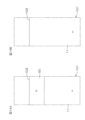
- FIG. 1 is a schematic plan view of a semiconductor device according to an embodiment of the present disclosure.
- FIG. 2 is a plan view showing an example of the layout of a plurality of IGBT regions, boundary regions, gate electrodes, and emitter electrodes.
- FIG. 3 is a plan view showing an example of the layout of gate wiring, boundary well regions, and peripheral well regions.
- FIG. 4 is an enlarged view of a portion enclosed by a dashed line IV in FIG.
- FIG. 5 is an enlarged view of a portion surrounded by a dashed line V in FIG.
- FIG. 6 is a cross-sectional view taken along the line VI-VI shown in FIG.
- FIG. 7 is a cross-sectional view taken along line VII-VII shown in FIG.
- FIG. 1 is a schematic plan view of a semiconductor device according to an embodiment of the present disclosure.
- FIG. 2 is a plan view showing an example of the layout of a plurality of IGBT regions, boundary regions, gate electrodes, and emit
- FIG. 8 is an enlarged view of a portion surrounded by a dashed line VIII in FIG.
- FIG. 9 is a cross-sectional view taken along line IX-IX shown in FIG.
- FIG. 10 is an enlarged view of the portion surrounded by the dashed line X in FIG.
- FIG. 11 is an enlarged view of a portion surrounded by a dashed line XI in FIG. 12A is a cross-sectional view taken along line XIIA-XIIA shown in FIG.
- FIG. 12B is an enlarged view of the portion surrounded by the dashed line XIIB in FIG.
- FIG. 13 is a schematic cross-sectional view for explaining the curvature index.
- 14A and 14B are diagrams showing a part of a manufacturing process of a semiconductor device according to an embodiment of the present disclosure.
- 15A and 15B are diagrams showing the next steps of FIGS. 14A and 14B, respectively.
- 16A and 16B are diagrams showing the next steps of FIGS. 15A and 15B, respectively.
- 17A and 17B are diagrams showing the next steps of FIGS. 16A and 16B, respectively.
- 18A and 18B are diagrams showing the next steps of FIGS. 17A and 17B, respectively.
- 19A and 19B are diagrams showing the next steps of FIGS. 18A and 18B, respectively.
- 20A and 20B are diagrams showing the next steps of FIGS. 19A and 19B, respectively.
- 21A and 21B are diagrams showing the next steps of FIGS.
- FIG. 20A and 20B are diagrams showing the next steps of FIGS. 21A and 21B, respectively.
- FIG. 23 is a diagram for explaining a patterning mask.
- FIG. 24 is a graph showing the relationship between the chamfer width and the curvature index of the patterning mask.
- FIG. 25 is a diagram showing the test results when an electrostatic breakdown resistance test (ESD resistance test) was performed on Example 1, Example 2, and Reference Examples 1 to 4.
- ESD resistance test electrostatic breakdown resistance test
- 26A to 26C are diagrams showing test results when a time-zero dielectric breakdown withstand test (TZBD withstand test) was performed on Reference Examples 1 to 3, respectively.
- 27A to 27C are diagrams showing test results when electrostatic breakdown resistance tests were performed on Reference Example 4, Example 1, and Example 2, respectively.
- FIG. 28 is a graph showing the relationship between the TCE treatment time and the amount of side etching of the trench.
- 29A to 29C are diagrams showing test results when a time zero dielectric breakdown withstand test (TZBD withstand test, 78 V) was performed on Reference Example 5, Example 3, and Example 4.
- 30A and 30B are diagrams showing test results when a time zero dielectric breakdown withstand test (TZBD withstand test, 84 V) was performed on Reference Example 5, Example 3, and Example 4.
- 31A and 31B are diagrams showing test results when a time zero dielectric breakdown withstand test (TZBD withstand test, 86 V) was performed on Reference Example 5, Example 3, and Example 4.
- FIG. 32 corresponds to FIG. 5 and is a cross-sectional view for explaining a modified example of the present disclosure.
- FIG. 1 is a schematic plan view of a semiconductor device 1 according to an embodiment of the present disclosure.
- FIG. 2 is a plan view showing an example layout of a plurality of IGBT regions 6, a boundary region 7, a gate electrode 71, and an emitter electrode 75.
- FIG. 3 is a plan view showing an example layout of a gate wiring 40, a boundary well region 50, and a peripheral well region 56.
- FIG. 4 is an enlarged view of a portion surrounded by a dashed line IV in FIG. 2.
- FIG. 5 is an enlarged view of a portion surrounded by a dashed line V in FIG. 4.
- FIG. 6 is a cross-sectional view taken along line VI-VI in FIG. 4.
- FIG. 4 is an enlarged view of a portion surrounded by a dashed line IV in FIG. 2.
- FIG. 5 is an enlarged view of a portion surrounded by a dashed line V in FIG. 4.
- FIG. 6 is a cross-sectional view taken along
- FIG. 7 is a cross-sectional view taken along line VII-VII in FIG. 4.
- FIG. 8 is an enlarged view of a portion surrounded by a dashed line VIII in FIG. 6.
- FIG. 9 is a cross-sectional view taken along line IX-IX in FIG. 5.
- FIG. 10 is an enlarged view of a portion surrounded by a dashed line X in FIG. 7.
- FIG. 11 is an enlarged view of a portion surrounded by a dashed line XI in FIG. 2.
- FIG. 12A is a cross-sectional view taken along line XIIA-XIIA in FIG. 11.
- FIG. 12B is an enlarged view of the portion surrounded by the dashed line XIIB in FIG. 11.
- FIG. 13 is a schematic plan view for explaining the curvature index CI.
- the semiconductor device 1 is an IGBT semiconductor device equipped with an IGBT (Insulated Gate Bipolar Transistor).
- the semiconductor device 1 includes a semiconductor chip 2 having a rectangular parallelepiped shape.
- the semiconductor chip 2 has a first main surface 3 on one side, a second main surface 4 on the other side, and side surfaces 5A, 5B, 5C, and 5D connecting the first main surface 3 and the second main surface 4.
- the first main surface 3 and the second main surface 4 are formed in a quadrangular shape when viewed in a plan view from their normal direction Z (hereinafter simply referred to as "plan view").
- the normal direction Z is also the thickness direction of the semiconductor chip 2.
- the first side surface 5A and the second side surface 5B extend in a first direction X along the first main surface 3 and face a second direction Y that intersects (specifically, is perpendicular to) the first direction X.
- the third side surface 5C and the fourth side surface 5D extend in the second direction Y and face the first direction X.
- the semiconductor chip 2 has a single-layer structure made of a silicon single crystal substrate.
- the semiconductor chip 2 is, for example, square in plan view.
- the size of the semiconductor chip 2 is, for example, 0.5 mm square or more and 20 mm square or less.
- a chip size of "X mm square” may mean that the length of one side of the square semiconductor chip 2 is X mm.
- the semiconductor device 1 includes a plurality of IGBT regions 6 formed at intervals in the second direction Y on the first main surface 3.
- Each IGBT region 6 includes a trench-type IGBT structure (transistor structure) Tr.
- the IGBT region 6 may be referred to as an "active region.”
- the plurality of IGBT regions 6 include a first IGBT region 6A and a second IGBT region 6B.
- the first IGBT region 6A is formed in a region on the first side surface 5A side of a line that crosses the center of the first main surface 3 in the first direction X.
- the second IGBT region 6B is formed in a region on the second side surface 5B side of a line that crosses the center of the first main surface 3 in the first direction X.
- the multiple IGBT regions 6 are each formed in a quadrangular ring shape having four sides parallel to the first to fourth side surfaces 5A to 5D in a plan view.
- the semiconductor device 1 further includes a boundary region 7 formed in a region between the multiple IGBT regions 6.
- the boundary region 7 is provided in a band shape extending in the first direction X in the region between the first IGBT region 6A and the second IGBT region 6B.
- the boundary region 7 is located on a straight line that crosses the center of the first main surface 3 in the first direction X.
- the boundary region 7 includes a first boundary region 8 having a relatively large width in the second direction Y, and a second boundary region 9 having a width in the second direction Y smaller than that of the first boundary region 8.
- the first boundary region 8 is provided in an area on one side in the first direction X (the third side surface 5C side) as a portion that supports the terminal electrode.
- the first boundary region 8 may also be referred to as a "pad region,” a "wide region,” or a "terminal support region.”
- the first boundary region 8 is located on a straight line that crosses the center of the first main surface 3 in the first direction X in a plan view, and is provided in a rectangular shape near the center of the third side surface 5C.
- the width of the first boundary region 8 may be 100 ⁇ m or more and 800 ⁇ m or less. It is preferable that the width of the first boundary region 8 is 200 ⁇ m or more and 600 ⁇ m or less. In this embodiment, the width of the first boundary region 8 is set in the range of 350 ⁇ m or more and 450 ⁇ m or less.
- the second boundary region 9 is formed in the region on the other side in the first direction X (the fourth side surface 5D side) of the first boundary region 8 as a portion that supports the wiring.
- the second boundary region 9 is located on a straight line that crosses the center of the first main surface 3 in the first direction X, and is pulled out in a strip shape from the first boundary region 8 toward the center of the fourth side surface 5D.
- the second boundary region 9 may also be called a "street region,” a "narrow width region,” or a "wiring support region.”
- the semiconductor device 1 further includes a peripheral region 10.
- the peripheral region 10 collectively surrounds the multiple IGBT regions 6.
- the peripheral region 10 is a quadrangular ring extending along the first to fourth side surfaces 5A to 5D.
- the peripheral region 10, together with the boundary region 7, forms an inactive region.
- the IGBT structure Tr which will be described later, is not formed in the boundary region 7 and the peripheral region 10.
- the semiconductor device 1 includes an n-type (first conductivity type) drift region 11.
- the drift region 11 is formed throughout the interior of the semiconductor chip 2.
- the semiconductor chip 2 is made of an n-type semiconductor substrate, and the drift region 11 is formed using this semiconductor substrate.
- the semiconductor device 1 further includes an n-type buffer region 12 formed in a surface layer portion of the second main surface 4.
- the buffer region 12 is formed in a layer extending along the second main surface 4 over the entire area of the second main surface 4.
- the buffer region 12 has a higher n-type impurity concentration than the drift region 11.
- the presence or absence of the buffer region 12 is optional, and a configuration without the buffer region 12 may be adopted.
- the semiconductor device 1 further includes a plurality of trench isolation structures 20 formed in the first main surface 3 so as to separate the multiple IGBT regions 6.
- a gate potential is applied to the multiple trench isolation structures 20.
- the trench isolation structures 20 may also be referred to as “trench gate isolation structures” or “trench gate connection structures.”
- the multiple trench isolation structures 20 include a first trench isolation structure 20A and a second trench isolation structure 20B.
- the first trench isolation structure 20A surrounds the first IGBT region 6A and separates the first IGBT region 6A from the boundary region 7 and the outer peripheral region 10.
- the first trench isolation structure 20A is formed in a polygonal ring shape having four sides parallel to the periphery of the semiconductor chip 2 in a plan view.
- the first trench isolation structure 20A has a bent portion that separates the first boundary region 8 and the second boundary region 9 of the boundary region 7 in a plan view.
- the second trench isolation structure 20B surrounds the second IGBT region 6B and separates the second IGBT region 6B from the boundary region 7 and the outer peripheral region 10.
- the second trench isolation structure 20B is formed in a polygonal ring shape having four sides parallel to the periphery of the semiconductor chip 2 in a plan view.
- the second trench isolation structure 20B has a bent portion that separates the first boundary region 8 and the second boundary region 9 of the boundary region 7 in a plan view.
- each trench isolation structure 20A, 20B includes at least two first direction portions 20X extending in a first direction X and at least two second direction portions 20Y extending in a second direction Y.
- the ends of the first direction portions 20X and the ends of the second direction portions 20Y are mechanically and electrically connected.
- the ends of the first direction portions 20X and the ends of the second direction portions 20Y intersect in an L-shape to form corners of the polygonal ring-shaped trench isolation structures 20A, 20B.
- Fig. 8 and Fig. 9 show a cross section of the trench isolation structure 20.
- Fig. 8 is a cross section perpendicular to the longitudinal direction of the trench isolation structure 20
- Fig. 9 is a cross section intersecting a T-shaped intersection 91P (described later) of the trench isolation structure 20.
- the trench isolation structure 20 includes an isolation trench 21 (first trench), an isolation insulating film 22, and an isolation buried electrode (buried conductor) 23.
- the isolation trench 21 is dug down from the first main surface 3 toward the second main surface 4, and defines the wall surface of the trench isolation structure 20.
- the isolation trench 21 is formed in the first main surface 3.
- the isolation trench 21 is formed in a vertical shape in a cross-sectional view.
- the isolation trench 21 includes a pair of side surfaces 21a, 21b facing each other, and a bottom surface 21c connecting the pair of side surfaces 21a, 21b.
- the bottom surface 21c has a rounded shape that bulges toward the second main surface 4 in a cross-sectional view.
- the isolation trench 21 has a first width W1 .
- the first width W1 is the width (maximum value) in a direction perpendicular to the direction in which the isolation trench 21 extends.
- the first width W1 is preferably less than the width of the second boundary region 9.
- the first width W1 is preferably not less than 0.5 ⁇ m and not more than 2.0 ⁇ m. More specifically, the first width W1 may be 1.0 ⁇ m.
- the isolation trench 21 has a first depth D1 .
- the first depth D1 may be 1 ⁇ m or more and 30 ⁇ m or less.
- the first depth D1 is preferably 4 ⁇ m or more and 15 ⁇ m or less.
- the first depth D1 is particularly preferably 6 ⁇ m or more and 10 ⁇ m or less.
- the isolation trench 21 may be formed in a tapered shape in which the width decreases toward the second main surface 4 in a cross-sectional view.
- the bottom surface 21c may be a flat surface parallel to the first main surface 3.
- a first recess 96 recessed toward the side surfaces 21a and 21b of the isolation trench 21 is formed at the opening ends 21d and 21e of the isolation trench 21.
- the cross-sectional shape of the first recess 96 is an arc recessed toward the side surfaces 21a and 21b of the isolation trench 21.
- the first recess 96 has a third width W3 .
- the third width W3 is the width in the second direction Y between the point where the extension of the side surfaces 21a and 21b intersects with the first main surface 3 and the end of the first recess 96.
- the third width W3 is 1350 ⁇ or more and 2000 ⁇ or less.
- the first recess 96 has a third depth D3 .
- the third depth D3 is greater than the third width W3 .
- the third depth D3 is 1850 ⁇ or more.
- the ratio (W 3 /W 1 ) of the third width W 3 to the first width W 1 of the isolation trench 21 is not less than 0.14 and not more than 0.2.
- the isolation insulating film 22 is formed in the form of a film along the side surfaces 21a, 21b of the isolation trench 21.
- the isolation insulating film 22 defines a recess space within the isolation trench 21.
- the isolation insulating film 22 may include at least one of a silicon oxide film, a silicon nitride film, a silicon oxynitride film, and an aluminum oxide film. It is preferable that the isolation insulating film 22 has a single-layer structure made of a single insulating film. It is particularly preferable that the isolation insulating film 22 includes a silicon oxide film made of an oxide of the semiconductor chip 2.
- the isolated buried electrode 23 is buried in the isolation trench 21 with the isolation insulating film 22 in between.
- the isolated buried electrode 23 is made of conductive polysilicon. A gate potential is applied to the isolated buried electrode 23.
- the structure on the second IGBT region 6B side is substantially the same as the structure on the first IGBT region 6A side. Specifically, the structure on the second IGBT region 6B side is linearly symmetrical to the structure on the first IGBT region 6A side with respect to the boundary region 7. Below, the structure on the first IGBT region 6A side will be described. The explanation of the structure on the second IGBT region 6B side will be omitted, as the explanation of the structure on the first IGBT region 6A side applies.
- the semiconductor device 1 includes a p-type base region 25 formed in the surface layer of the first main surface 3 in the first IGBT region 6A.
- the base region 25 may also be called a "body region” or a "channel region.”
- the base region 25 is formed at a depth shallower than the trench isolation structure 20, and has a bottom located closer to the first main surface 3 than the bottom wall of the trench isolation structure 20.
- the base region 25 extends in a layered manner along the first main surface 3, and is connected to the inner peripheral wall of the trench isolation structure 20.
- the semiconductor device 1 includes a plurality of trench structures 30.
- a gate potential is applied to the plurality of trench structures 30.
- the plurality of trench structures 30 penetrate the base region 25 and reach the drift region 11.
- the plurality of trench structures 30 are arranged at intervals in the first direction X in a plan view, and are each formed in a band shape extending in the second direction Y. In other words, the plurality of trench structures 30 are arranged in a stripe shape extending in the second direction Y.
- the multiple trench structures 30 each have a first end 30A on the boundary region 7 side and a second end 30B on the outer periphery region 10 side in the longitudinal direction (second direction Y).
- the first end 30A and the second end 30B are mechanically and electrically connected to the trench isolation structure 20.
- the multiple trench structures 30 and the trench isolation structure 20 form a ladder-shaped trench gate structure.
- the connection portion between the trench structure 30 and the trench isolation structure 20 may be considered as part of the trench isolation structure 20 or may be considered as part of the trench structure 30.
- the trench structure 30 includes a gate trench 31 (second trench), a gate insulating film 32, and a gate buried electrode (buried conductor) 33.
- the gate trench 31 is dug down from the first main surface 3 toward the second main surface 4, and defines the wall surface of the trench structure 30.
- the gate trench 31 is formed in the first main surface 3.
- the gate trench 31 is formed in a vertical shape in a cross-sectional view.
- the gate trench 31 includes a pair of side surfaces 31a, 31b facing each other and a bottom surface 31c connecting the pair of side surfaces 31a, 31b.
- the bottom surface 31c has a rounded shape that bulges toward the second main surface 4 in a cross-sectional view.
- the gate trench 31 is connected to the separation trench 21 at both ends (first end 30A and second end 30B) in the second direction Y.
- the side wall of the gate trench 31 is connected to the side wall of the separation trench 21, and the bottom wall of the gate trench 31 is connected to the bottom wall of the separation trench 21.
- the multiple gate trenches 31 are arranged at a constant pitch P in the first direction X.
- the pitch P of the multiple gate trenches 31 is preferably less than the width of the second boundary region 9 of the boundary region 7.
- the pitch P of the multiple gate trenches 31 may be 5 ⁇ m or more and 30 ⁇ m or less.
- the pitch P of the multiple gate trenches 31 is preferably 10 ⁇ m or more and 20 ⁇ m or less.
- the pitch P of the multiple gate trenches 31 is preferably 15 ⁇ m.
- the gate trench 31 has a second width W2 .
- the second width W2 is the width (maximum value) in a direction perpendicular to the direction in which the gate trench 31 extends.
- the second width W2 is preferably 0.5 ⁇ m or more and 2.0 ⁇ m or less. More specifically, the second width W2 may be 1.0 ⁇ m.
- the second width W2 may be approximately equal to the first width W1 .
- the gate trench 31 has a second depth D2 .
- the second depth D2 may be 1 ⁇ m or more and 30 ⁇ m or less.
- the second depth D2 is preferably 4 ⁇ m or more and 15 ⁇ m or less.
- the second depth D2 is particularly preferably 6 ⁇ m or more and 10 ⁇ m or less.
- the second depth D2 is preferably approximately equal to the first depth D1 .
- the gate trench 31 may be formed in a tapered shape in which the width decreases toward the second main surface 4 in a cross-sectional view.
- the bottom surface 31c may be a flat surface parallel to the first main surface 3.
- a second recess 97 recessed toward the side surfaces 31a and 31b of the gate trench 31 is formed at the opening ends 31d and 31e of the gate trench 31.
- the cross-sectional shape of the second recess 97 is an arc recessed toward the side surfaces 31a and 31b of the gate trench 31.
- the second recess 97 has a fourth width W4 .
- the fourth width W4 is the width in the first direction X between the point where the extension line of the side surfaces 31a and 31b intersects with the first main surface 3 and the end of the second recess 97.
- the fourth width W4 is 1350 ⁇ or more and 2000 ⁇ or less.
- the second recess 97 has a fourth depth D4 .
- the fourth depth D4 is greater than the fourth width W4 .
- the fourth depth D4 is 1850 ⁇ or more.
- the ratio ( W4 / W2 ) of the fourth width W4 to the second width W2 of the gate trench 31 is 0.14 or more and 0.2 or less.
- the ratio ( W4 /P) of the fourth width W4 to the pitch P (described later) of the multiple gate trenches 31 is 0.009 or more and 0.0133 or less.
- the ratio ( W4 /W5) of the fourth width W4 to the fifth width W5 (described later) of the mesa portion 90 (described later) is 0.011 or more and 0.017 or less.
- the gate insulating film 32 is formed in the form of a film along the wall surface of the gate trench 31.
- the gate insulating film 32 defines a recess space within the gate trench 31.
- the thickness of the gate insulating film 32 is, for example, 50 nm or more and 200 nm or less.
- the gate insulating film 32 may include at least one of a silicon oxide film, a silicon nitride film, a silicon oxynitride film, and an aluminum oxide film.
- the gate insulating film 32 preferably has a single-layer structure made of a single insulating film. It is particularly preferable that the gate insulating film 32 includes a silicon oxide film made of an oxide of the semiconductor chip 2. In this embodiment, the gate insulating film 32 is made of the same insulating film as the isolation insulating film 22. The gate insulating film 32 is connected to the isolation insulating film 22 at the communicating portion between the isolation trench 21 and the gate trench 31.
- the gate buried electrode 33 is buried in the gate trench 31 with the gate insulating film 32 sandwiched therebetween.
- the gate buried electrode 33 is made of conductive polysilicon.
- a gate potential is applied to the gate buried electrode 33.
- the gate buried electrode 33 is connected to the isolation buried electrode 23 at the communicating portion between the isolation trench 21 and the gate trench 31.
- the semiconductor device 1 further includes a plurality of n-type emitter regions 35 formed in a surface layer portion of the base region 25.
- Each of the plurality of emitter regions 35 has a higher n-type impurity concentration than the drift region 11.
- the plurality of emitter regions 35 are formed on both sides of the plurality of trench structures 30.
- the plurality of emitter regions 35 are each formed in a band shape extending along the plurality of trench structures 30 in a planar view.
- the plurality of emitter regions 35 may be formed at intervals along the plurality of trench structures 30 in a planar view.
- the semiconductor device 1 further includes a plurality of n-type carrier storage regions 36 formed in the semiconductor chip 2 in the region directly below the base region 25.
- the plurality of carrier storage regions 36 suppress the discharge of carriers (positive holes) into the base region 25 and promote the accumulation of carriers (positive holes) in the region directly below the plurality of trench structures 30.
- the plurality of carrier storage regions 36 promote low on-resistance and low on-voltage from within the semiconductor chip 2.
- the carrier storage regions 36 are arranged on both sides of the trench structures 30, and are formed in a strip shape extending along the trench structures 30 in a plan view.
- the carrier storage regions 36 are formed in the region between the bottom of the base region 25 and the bottom wall of the trench structure 30 in the thickness direction of the semiconductor chip 2.
- the carrier storage regions 36 are preferably spaced apart from the bottom wall of the trench structure 30 toward the base region 25.
- the bottoms of the carrier storage regions 36 are preferably located closer to the bottom wall of the trench structure 30 than the middle part of the trench structure 30.
- the carrier storage regions 36 have a higher n-type impurity concentration than the drift region 11.
- the n-type impurity concentration of the carrier storage regions 36 is preferably lower than that of the emitter region 35.
- the presence or absence of the carrier storage regions 36 is optional. Therefore, a configuration without the carrier storage regions 36 may be adopted.
- the semiconductor device 1 includes a plurality of contact holes 37 formed in the first main surface 3 to expose the emitter regions 35.
- the plurality of contact holes 37 are formed on both sides of the plurality of trench structures 30 at intervals in the first direction X from the plurality of trench structures 30.
- the plurality of contact holes 37 may each be formed in a tapered shape in which the opening width narrows from the opening toward the bottom wall.
- the multiple contact holes 37 may be spaced from the bottom of the emitter region 35 toward the first main surface 3 so as not to reach the base region 25.
- the multiple contact holes 37 may penetrate the emitter region 35 so as to reach the base region 25.
- the multiple contact holes 37 are each formed in a band shape extending along the multiple trench structures 30 in a plan view. In the longitudinal direction (second direction Y), the multiple contact holes 37 are shorter than the multiple trench structures 30.
- the semiconductor device 1 includes a plurality of p-type contact regions 38 formed in a region different from the plurality of emitter regions 35 in the surface layer portion of the base region 25.
- the plurality of contact regions 38 are each formed in a strip shape extending along the corresponding contact hole 37 in a plan view.
- the bottoms of the plurality of contact regions 38 are each formed in a region between the bottom wall of the corresponding contact hole 37 and the bottom of the base region 25.
- the plurality of contact regions 38 have a higher p-type impurity concentration than the base region 25.
- the base region 25, the multiple trench structures 30, the multiple emitter regions 35, the multiple carrier storage regions 36, the multiple contact holes 37 and the multiple contact regions 38 are included in the IGBT structure Tr (see Figures 2 and 4).
- the semiconductor device 1 includes a plurality of mesa portions 90 defined in the first IGBT region 6A.
- the plurality of mesa portions 90 are defined by gate trenches 31.
- Each mesa portion 90 is defined in a region between a pair of gate trenches 31 adjacent to each other in the first direction X.
- the mesa portion 90 is made up of a part of the semiconductor chip 2.
- the plurality of mesa portions 90 each extend in a band shape extending in the second direction Y, and are defined at intervals in the first direction X. In other words, the plurality of mesa portions 90 are formed in a stripe shape extending in the second direction Y.
- the mesa portion 90 has a fifth width W5 .
- the fifth width W5 is the width (maximum value) in a direction perpendicular to the direction in which the mesa portion 90 extends.
- the fifth width W5 is preferably less than the width of the second boundary region 9.
- the fifth width W5 may be 11 ⁇ m or more and 21 ⁇ m or less. It is preferable that the fifth width W5 is 11 ⁇ m or more and 16 ⁇ m or less. It is preferable that the fifth width W5 is 14 ⁇ m.
- the semiconductor device 1 includes a p-type boundary well region 50 formed in the surface layer of the first main surface 3 in the boundary region 7.
- the boundary well region 50 has a higher p-type impurity concentration than the multiple base regions 25.
- the boundary well region 50 may have a lower p-type impurity concentration than the multiple base regions 25.
- the boundary well region 50 is formed in a region sandwiched between the first trench isolation structure 20A and the second trench isolation structure 20B.
- the boundary well region 50 extends in the first direction X along the boundary region 7 in a plan view.
- the boundary well region 50 includes a first boundary well region 51 formed in the first boundary region 8 of the boundary region 7, and a second boundary well region 52 formed in the second boundary region 9 of the boundary region 7.
- the first boundary well region 51 has a relatively large region width in the second direction Y.
- the first boundary well region 51 is formed in a quadrangular shape in a plan view. It is preferable that the first boundary well region 51 is formed over the entire area of the first boundary region 8.
- the second boundary well region 52 has a width in the second direction Y that is smaller than the width of the first boundary well region 51, and is pulled out in a strip shape from the first boundary well region 51 toward the second boundary region 9.
- the second boundary well region 52 is located on a straight line that crosses the center of the first main surface 3 in the first direction X.
- the boundary well region 50 is formed deeper than the base region 25.
- the boundary well region 50 is preferably formed deeper than the multiple trench isolation structures 20.
- the boundary well region 50 has a width in the second direction Y that is greater than the width of the boundary region 7, and is pulled out from the boundary region 7 into the multiple IGBT regions 6.
- the boundary well region 50 is connected to multiple trench isolation structures 20 adjacent in the second direction Y.
- the boundary well region 50 has a portion that covers the bottom walls of the multiple trench isolation structures 20.
- the boundary well region 50 has a portion that crosses the multiple trench isolation structures 20 and covers the bottom walls of the multiple trench structures 30.
- the boundary well region 50 covers the sidewalls of the trench isolation structure 20 in each IGBT region 6. Although not shown, the boundary well region 50 covers the sidewalls of multiple trench structures 30 in each IGBT region 6. As shown in FIGS. 4 and 7, the boundary well region 50 is connected to each base region 25 in the surface layer of the first main surface 3.
- the semiconductor device 1 includes a p-type peripheral well region 56 formed in the surface layer of the first main surface 3 in the peripheral region 10.
- the peripheral well region 56 has a higher p-type impurity concentration than the multiple base regions 25.
- the peripheral well region 56 may have a lower p-type impurity concentration than the multiple base regions 25. It is preferable that the p-type impurity concentration of the peripheral well region 56 is approximately equal to the p-type impurity concentration of the boundary well region 50.
- the peripheral well region 56 is formed in a layer extending along the first main surface 3 and is exposed from the first main surface 3.
- the peripheral well region 56 is formed at a distance inward from the periphery (first to fourth side surfaces 5A to 5D) of the first main surface 3.
- the peripheral well region 56 is formed in a band shape extending along the multiple IGBT regions 6 in a planar view.
- the peripheral well region 56 is formed in a ring shape surrounding the multiple IGBT regions 6 in a planar view.
- the peripheral well region 56 is formed in a quadrangular ring shape having four sides parallel to the periphery of the first main surface 3.
- the peripheral well region 56 is formed deeper than the multiple base regions 25. It is particularly preferable that the peripheral well region 56 is formed deeper than the multiple trench isolation structures 20 (multiple trench structures 30). In this embodiment, the peripheral well region 56 has a depth approximately equal to that of the boundary well region 50.
- the peripheral well region 56 is connected to the multiple trench isolation structures 20.
- the peripheral well region 56 has a portion that covers the bottom walls of the multiple trench isolation structures 20.
- the peripheral well region 56 is extended from the peripheral region 10 into each IGBT region 6 (see FIG. 3).
- the peripheral well region 56 has a portion that crosses the multiple trench isolation structures 20 and covers the bottom walls of the multiple trench structures 30.
- the IGBT structure Tr includes a plurality of T-shaped intersections 91P formed at the connection portion between the trench isolation structure 20 and the trench structure 30.
- the plurality of T-shaped intersections 91P include a plurality of first T-shaped intersections 91PA (FIG. 4) formed at the connection portion between the first end portion 30A of the trench structure 30 and the first direction portion 20X on the boundary region 7 side of the trench isolation structure 20, and a plurality of second T-shaped intersections 91PB (FIG. 11) formed at the connection portion between the second end portion 30B of the trench structure 30 and the first direction portion 20X on the peripheral region 10 side of the trench isolation structure 20.
- the first T-shaped intersections 91PA face the boundary wiring 42 and boundary well region 50 (second boundary well region 52) in the thickness direction of the semiconductor chip 2.
- the second T-shaped intersections 91PB face the first peripheral wiring 43 and peripheral well region 56 in the thickness direction of the semiconductor chip 2.
- the T-shaped intersection 91P has two corners 92P.
- the curvature index CI P of each corner 92P is equal to or greater than 1.5 ⁇ m and equal to or less than 2.4 ⁇ m.
- the curvature index CI P is the curvature index CI of the corner 92P (see FIG. 13).
- the curvature index CI is an index for defining the curvature of the corners (corner 92P, corner 92Q).
- the corners (corner 92P, corner 92Q) are formed by a first side 93 and a second side 94.
- the curvature index CI is the shortest distance between the intersection point P1 of an extension line E1 of the first side 93 that forms the corner (corner 92P, corner 92Q) and an extension line E2 of the second side 94 that is perpendicular to the extension line E1 and forms the corner (corner 92P, corner 92Q), and the corner (corner 92P, corner 92Q).
- it is the shortest distance between the intersection point P1 and a tangent line TL of the corner (corner 92P, corner 92Q) that intersects both the extension line E1 and the extension line E2 at 45°.
- the ratio (CI P /W 1 ) of the curvature index CI P of the corner 92P to the first width W 1 of the isolation trench 21 is 1.5 or more and 2.4 or less.
- the ratio (CI P /W 2 ) of the curvature index CI P of the corner 92P to the second width W 2 of the multiple gate trenches 31 is 1.5 or more and 2.4 or less.
- the ratio (CI P /P) of the curvature index CI P of the corner 92P to the pitch P of the multiple gate trenches 31 is 0.1 or more and 0.16 or less.
- the ratio (CI P /W 5 ) of the curvature index CI P of the corner 92P to the fifth width W 5 of the mesa portion 90 is not less than 0.11 and not more than 0.17.
- the IGBT structure Tr includes a plurality of L-shaped intersections 91Q formed at the connection between the first direction portion 20X of the trench isolation structure 20 and the second direction portion 20Y of the trench isolation structure 20.
- the plurality of L-shaped intersections 91Q include a plurality of first L-shaped intersections 91 (not shown) formed at the connection between the first direction portion 20X and the second direction portion 20Y on the boundary region 7 side of the trench isolation structure 20, and a plurality of second L-shaped intersections 91QB formed at the connection between the first direction portion 20X and the second direction portion 20Y on the peripheral region 10 side of the trench isolation structure 20.
- the multiple first L-shaped intersections 91 face the boundary wiring 42 and boundary well region 50 (second boundary well region 52) in the thickness direction of the semiconductor chip 2.
- the multiple second L-shaped intersections 91QB face the first peripheral wiring 43 and peripheral well region 56 in the thickness direction of the semiconductor chip 2.
- the L-shaped intersection 91Q has one corner 92Q.
- the curvature index of the corner 92Q is 1.5 ⁇ m or more and 2.4 ⁇ m or less.
- the curvature index CI P is the curvature index CI of the corner 92Q (see FIG. 13).
- a ratio (CI Q /W 1 ) of the curvature index CI Q of the corner 92Q to the first width W 1 of the isolation trench 21 is 1.5 or more and 2.4 or less.
- a ratio (CI Q /W 2 ) of the curvature index CI Q of the corner 92Q to the second width W 2 of the multiple gate trenches 31 is 1.5 or more and 2.4 or less.
- a ratio (CI Q /P) of the curvature index CI Q of the corner 92P to the pitch P of the multiple gate trenches 31 is 0.1 or more and 0.16 or less.
- the ratio (CI Q /W 5 ) of the curvature index CI Q of the corner 92Q to the fifth width W 5 of the mesa portion 90 is not less than 0.11 and not more than 0.17.
- the semiconductor device 1 includes a main surface insulating film 39 that covers the first main surface 3.
- the thickness of the main surface insulating film 39 is, for example, 50 nm or more and 200 nm or less.
- the main surface insulating film 39 may include at least one of a silicon oxide film, a silicon nitride film, a silicon oxynitride film, and an aluminum oxide film. It is preferable that the main surface insulating film 39 has a single-layer structure made of a single insulating film. It is particularly preferable that the main surface insulating film 39 includes a silicon oxide film made of an oxide of the semiconductor chip 2. In this embodiment, the main surface insulating film 39 is made of the same insulating film as the gate insulating film 32.
- the main surface insulating film 39 extends in the form of a film along the first main surface 3 so as to cover the multiple IGBT regions 6, the boundary region 7 and the peripheral region 10.
- the main surface insulating film 39 may be continuous with the periphery (first to fourth side surfaces 5A to 5D) of the semiconductor chip 2.
- the main surface insulating film 39 covers the first main surface 3 so as to expose the multiple trench isolation structures 20 and the multiple trench structures 30. Specifically, the main surface insulating film 39 is connected to the isolation insulating film 22 and the gate insulating film 32, and exposes the isolation buried electrode 23 and the gate buried electrode 33.
- the semiconductor device 1 includes a gate wiring 40 disposed on the first main surface 3 of the semiconductor chip 2.
- the gate wiring 40 is disposed in the form of a film on the main surface insulating film 39.
- the gate wiring 40 is made of a conductive polysilicon film.
- the gate wiring 40 is routed at least in the boundary region 7.
- the gate wiring 40 is routed in the boundary region 7 and the outer peripheral region 10 in an arbitrary layout.
- the gate wiring 40 includes a pad wiring 41, a boundary wiring 42, a first outer peripheral wiring 43, and a second outer peripheral wiring 44.
- the pad wiring 41 is disposed on the first boundary region 8 of the boundary region 7, and has a relatively large first wiring width in the second direction Y.
- the pad wiring 41 is formed in a quadrangular shape in a plan view.
- the pad wiring 41 has a width in the second direction Y that is larger than the width of the boundary region 7 (the width of the first boundary region 8).
- the pad wiring 41 is drawn out from above the boundary region 7 onto a plurality of trench isolation structures 20 adjacent in the second direction Y.
- the pad wiring 41 is drawn out from above the boundary region 7 onto the multiple IGBT regions 6. As a result, the pad wiring 41 is mechanically and electrically connected to the isolated buried electrode 23 and the multiple gate buried electrodes 33, and transmits the gate potential to the isolated buried electrode 23 and the gate buried electrode 33. In this embodiment, the pad wiring 41 is formed integrally with the isolated buried electrode 23 and the multiple gate buried electrodes 33.
- the boundary wiring 42 is drawn from the pad wiring 41 onto the second boundary region 9 of the boundary region 7, and has a second wiring width in the second direction Y that is smaller than the first wiring width of the pad wiring 41.
- the boundary wiring 42 is formed in a band shape extending in the first direction X. In this embodiment, the boundary wiring 42 crosses the center of the semiconductor chip 2.
- the boundary wiring 42 has a width in the second direction Y that is larger than the width of the boundary region 7 (the width of the second boundary region 9).
- the boundary wiring 42 is drawn from above the boundary region 7 onto a plurality of trench isolation structures 20 adjacent in the second direction Y.
- the boundary wiring 42 is drawn from above the boundary region 7 to above the multiple IGBT regions 6 so as to cover the first ends 30A of the multiple trench structures 30.
- the boundary wiring 42 is mechanically and electrically connected to the isolated buried electrode 23 and the multiple gate buried electrodes 33, and transmits the gate potential to the isolated buried electrode 23 and the gate buried electrode 33.
- the boundary wiring 42 is formed integrally with the isolated buried electrode 23 and the multiple gate buried electrodes 33.
- the first peripheral wiring 43 is pulled out from the pad wiring 41 onto the peripheral region 10 and is formed in a band extending along the first side surface 5A and the third side surface 5C.
- the first peripheral wiring 43 may have a portion that extends in a band along the fourth side surface 5D.
- the first peripheral wiring 43 has a portion that is pulled out from above the peripheral region 10 onto the first trench isolation structure 20A in the portion that extends along the first side surface 5A.
- the first peripheral wiring 43 also covers the second ends 30B of the multiple trench structures 30 in the first IGBT region 6A.
- the first peripheral wiring 43 is mechanically and electrically connected to the isolated buried electrode 23 and the multiple gate buried electrodes 33.
- the first peripheral wiring 43 is formed integrally with the isolated buried electrode 23 and the multiple gate buried electrodes 33.
- the first peripheral wiring 43 transmits the gate potential from the peripheral region 10 side to the isolated buried electrode 23 and the gate buried electrode 33.
- the second peripheral wiring 44 is pulled out from the pad wiring 41 onto the peripheral region 10 and is formed in a band extending along the second side surface 5B and the third side surface 5C.
- the second peripheral wiring 44 may have a portion that extends in a band along the fourth side surface 5D.
- the second peripheral wiring 44 has a portion that is pulled out from above the peripheral region 10 onto the second trench isolation structure 20B in the portion that extends along the second side surface 5B.
- the second peripheral wiring 44 also covers the second ends 30B of the multiple trench structures 30 in the second IGBT region 6B.
- the second peripheral wiring 44 is mechanically and electrically connected to the isolated buried electrode 23 and the multiple gate buried electrodes 33.
- the second peripheral wiring 44 is formed integrally with the isolated buried electrode 23 and the multiple gate buried electrodes 33.
- the second peripheral wiring 44 transmits the gate potential from the peripheral region 10 side to the isolated buried electrode 23 and the gate buried electrode 33.
- the semiconductor device 1 further includes an interlayer insulating film 60 that covers the main surface insulating film 39.
- the interlayer insulating film 60 may include at least one of a silicon oxide film, a silicon nitride film, a silicon oxynitride film, and an aluminum oxide film.
- the interlayer insulating film 60 may include at least one of an NSG (Non-doped Silicate Glass) film, a PSG (Phosphor Silicate Glass) film, and a BPSG (Boron Phosphor Silicate Glass) film, which are examples of silicon oxide films.
- the interlayer insulating film 60 may have a single-layer structure made of a single insulating film, or a layered structure including multiple insulating films.
- the interlayer insulating film 60 has a thickness that exceeds the thickness of the main surface insulating film 39.
- the thickness of the interlayer insulating film 60 is, for example, 1.0 ⁇ m or more and 2.5 ⁇ m or less.
- the interlayer insulating film 60 may extend in a layered manner along the first main surface 3 and be continuous with the periphery (first to fourth side surfaces 5A to 5D) of the semiconductor chip 2.
- the interlayer insulating film 60 selectively covers the multiple IGBT regions 6, the boundary region 7 and the peripheral region 10.
- the interlayer insulating film 60 covers the main surface insulating film 39, the multiple trench isolation structures 20 and the multiple trench structures 30 in each IGBT region 6.
- the interlayer insulating film 60 covers the main surface insulating film 39 and the gate wiring 40 in the boundary region 7 and the peripheral region 10.
- the interlayer insulating film 60 has a plurality of contact openings 61 that expose a plurality of emitter regions 35 in each IGBT region 6.
- the plurality of contact openings 61 are formed in a one-to-one correspondence with the plurality of contact holes 37, and each communicates with the corresponding contact hole 37.
- the plurality of contact openings 61 are each formed in a band shape extending along the corresponding contact hole 37 in a plan view.
- the interlayer insulating film 60 includes at least one gate opening that selectively exposes the gate wiring 40 in the boundary region 7 and/or the peripheral region 10.
- the gate opening may expose the boundary wiring 42, the first peripheral wiring 43, and the second peripheral wiring 44.
- FIG. 12A shows only the gate opening 62 that exposes the first peripheral wiring 43.
- the interlayer insulating film 60 includes at least one (in this embodiment, multiple) first well openings 63 that selectively expose the inner edge of the peripheral well region 56 in the peripheral region 10. Specifically, the multiple first well openings 63 expose the inner edge of the peripheral well region 56 in the region between the multiple trench isolation structures 20 and the gate wiring 40.
- the interlayer insulating film 60 includes at least one (one in this embodiment) second well opening 64 that selectively exposes the outer edge of the peripheral well region 56 in the peripheral region 10.
- the second well opening 64 exposes the outer edge of the peripheral well region 56 in a region closer to the peripheral side of the first main surface 3 than the gate wiring 40.
- the second well opening 64 is formed in a band shape extending along the multiple IGBT regions 6.
- the second well opening 64 is formed in a square ring shape surrounding the multiple IGBT regions 6.
- the interlayer insulating film 60 includes at least one (two in this embodiment) boundary gate opening 81 (see also FIG. 4) that exposes the boundary wiring 42 of the gate wiring 40.
- the multiple boundary gate openings 81 are each formed in a strip extending in the first direction X and are formed at intervals in the second direction Y.
- the planar shape of the boundary gate opening 81 is arbitrary.
- the boundary gate opening 81 may be formed in a circular, elliptical, rectangular or polygonal shape in a planar view.
- the multiple boundary gate openings 81 may be arranged at intervals in the first direction X.
- the number of boundary gate openings 81 is arbitrary.
- the semiconductor device 1 includes a plurality of via electrodes 70 embedded in the interlayer insulating film 60 so as to be electrically connected to the plurality of emitter regions 35.
- the plurality of via electrodes 70 are embedded in a plurality of contact openings 61 in the interlayer insulating film 60.
- the plurality of via electrodes 70 include a portion in contact with the semiconductor chip 2 and a portion in contact with the interlayer insulating film 60.
- the plurality of via electrodes 70 are electrically connected to the emitter regions 35 and the contact regions 38 in the portion in contact with the semiconductor chip 2.
- Each via electrode 70 may include at least one of a Ti-based metal film, a W-based metal film, an Al-based metal film, and a Cu-based metal film.
- the Ti-based metal may include at least one of a pure Ti film (a Ti film having a purity of 99% or more) and a Ti alloy film.
- the Ti alloy film may be a TiN film.
- the W-based metal may include at least one of a pure W film (a W film having a purity of 99% or more) and a W alloy film.
- the Al-based metal may include at least one of a pure Al film (an Al film having a purity of 99% or more) and an Al alloy film.
- the Al alloy film may include at least one of an AlCu alloy, an AlSi alloy, and an AlSiCu alloy.
- the Cu-based metal may include at least one of a pure Cu film (a Cu film having a purity of 99% or more) and a Cu alloy film.
- Each via electrode 70 may have a layered structure including a Ti-based metal film and a W-based metal film.
- the semiconductor device 1 includes a plurality of gate via electrodes 82 embedded in a plurality of boundary gate openings 81 so as to be mechanically and electrically connected to the boundary wiring 42.
- Each gate via electrode 82 may include at least one of a Ti-based metal film, a W-based metal film, an Al-based metal film, and a Cu-based metal film.
- Each gate via electrode 82 may have a layered structure including a Ti-based metal film and a W-based metal film, similar to the via electrode 70.
- the multiple gate via electrodes 82 preferably face the gate wiring 40 (boundary wiring 42) and the boundary well region 50 (second boundary well region 52) in the thickness direction of the semiconductor chip 2.
- the semiconductor device 1 includes a gate electrode 71 disposed on the interlayer insulating film 60 so as to be electrically connected to the gate wiring 40.
- the gate electrode 71 is made of a conductive material different from that of the gate wiring 40.
- the gate electrode 71 is made of a metal film and has a lower resistance value than the gate wiring 40.
- the gate electrode 71 may be referred to as a "gate metal.”
- the gate electrode 71 may include at least one of a Ti-based metal film, a W-based metal film, an Al-based metal film, and a Cu-based metal film.
- the gate electrode 71 may have a layered structure including a Ti-based metal film and an Al-based metal film.
- the gate electrode 71 is disposed directly above the gate wiring 40.
- the gate electrode 71 can be routed in any layout to any of the multiple IGBT regions 6, the boundary region 7, and the peripheral region 10 depending on the layout of the gate wiring 40.
- the gate electrode 71 includes a gate pad electrode 72, a first gate finger electrode 73, a second gate finger electrode 74, and a boundary gate finger electrode 83.
- a capacitor is formed by a gate electrode 71 and an IGBT structure Tr facing the gate electrode 71 via an interlayer insulating film 60.
- the capacitance of the capacitor as a whole gate is 300 pF or less.
- the gate pad electrode 72 is disposed directly above the pad wiring 41 of the gate wiring 40.
- the gate pad electrode 72 enters the gate opening (not shown) from above the interlayer insulating film 60 and is electrically connected to the pad wiring 41.
- the gate pad electrode 72 is formed in a rectangular shape in a plan view.
- the gate pad electrode 72 faces the first boundary well region 51 of the boundary well region 50 in the thickness direction of the semiconductor chip 2.
- the gate pad electrode 72 is preferably formed spaced apart from the trench isolation structure 20 and the multiple trench structures 30 in a plan view.
- the gate pad electrode 72 preferably has a planar area smaller than the planar area of the first boundary well region 51 of the boundary well region 50. It is particularly preferable that the gate pad electrode 72 has a planar area smaller than the planar area of the pad wiring 41.
- the first gate finger electrode 73 is drawn out from the gate pad electrode 72 directly above the first outer peripheral wiring 43.
- the first gate finger electrode 73 is formed in a band shape extending along the first outer peripheral wiring 43.
- the first gate finger electrode 73 extends in a band shape along the first side surface 5A and the third side surface 5C.
- the first gate finger electrode 73 enters the gate opening 62 from above the interlayer insulating film 60 and is electrically connected to the first peripheral wiring 43.
- the first gate finger electrode 73 faces the peripheral well region 56 in the thickness direction of the semiconductor chip 2.
- the first gate finger electrode 73 is preferably formed at a distance from the trench isolation structure 20 and the multiple trench structures 30 in a plan view.
- the second gate finger electrode 74 is drawn out from the gate pad electrode 72 directly above the second peripheral wiring 44.
- the second gate finger electrode 74 is formed in a band shape extending along the second peripheral wiring 44.
- the second gate finger electrode 74 extends in a band shape along the second side surface 5B and the third side surface 5C.
- the second gate finger electrode 74 is electrically connected to the second peripheral wiring 44 through a gate opening (not shown) from above the interlayer insulating film 60. If a via electrode similar to the via electrode 70 is embedded in the gate opening, the second gate finger electrode 74 may be electrically connected to the second peripheral wiring 44 through the via electrode.
- the second gate finger electrode 74 faces the peripheral well region 56 in the thickness direction of the semiconductor chip 2. It is preferable that the second gate finger electrode 74 is formed at a distance from the trench isolation structure 20 and the multiple trench structures 30 in a plan view.
- the boundary gate finger electrode 83 is drawn out from the gate pad electrode 72 directly above the boundary wiring 42.
- the boundary gate finger electrode 83 is formed in a strip shape extending along the boundary wiring 42 so as to cover the multiple gate via electrodes 82.
- the boundary gate finger electrode 83 is electrically connected to the boundary wiring 42 through a plurality of gate via electrodes 82.
- the boundary gate finger electrode 83 faces the gate wiring 40 (boundary wiring 42) and the boundary well region 50 (second boundary well region 52) in the thickness direction of the semiconductor chip 2.
- the boundary gate finger electrode 83 has a width smaller than the width of the boundary well region 50, and has a periphery located on the boundary region 7 side of the periphery of the boundary well region 50.
- the boundary gate finger electrode 83 has a width smaller than the width of the boundary wiring 42, and has a periphery located on the boundary region 7 side of the periphery of the boundary wiring 42.
- the boundary gate finger electrode 83 has a width smaller than the width of the boundary region 7, and has a periphery located inward from the periphery of the boundary region 7.
- the boundary gate finger electrode 83 is disposed only directly above the boundary region 7 in a plan view, and is not disposed above each IGBT region 6. Specifically, the boundary gate finger electrode 83 is disposed above the boundary region 7 at a distance from the multiple trench structures 30 of the first IGBT region 6A and the multiple trench structures 30 of the second IGBT region 6B in a plan view. The boundary gate finger electrode 83 is disposed above the boundary region 7 at a distance from the first trench isolation structure 20A and the second trench isolation structure 20B in a plan view.
- the semiconductor device 1 includes an emitter electrode 75 disposed on the interlayer insulating film 60 at a distance from the gate wiring 40.
- the emitter electrode 75 is made of a conductive material different from that of the gate wiring 40.
- the emitter electrode 75 is made of a metal film.
- the emitter electrode 75 may be referred to as an "emitter metal.”
- the emitter electrode 75 may include at least one of a Ti-based metal film, a W-based metal film, an Al-based metal film, and a Cu-based metal film.
- the emitter electrode 75 may have a layered structure including a Ti-based metal film and an Al-based metal film.
- the emitter electrode 75 is disposed on the interlayer insulating film 60 so as to cover the multiple IGBT regions 6.
- the emitter electrode 75 collectively covers the multiple via electrodes 70, and is electrically connected to the multiple emitter regions 35 via the multiple via electrodes 70.
- the emitter electrode 75 has a portion that covers the boundary wiring 42 of the gate wiring 40 with the interlayer insulating film 60 in between.
- the emitter electrode 75 has a portion that faces the gate wiring 40 (boundary wiring 42) and the boundary well region 50 in the thickness direction of the semiconductor chip 2.
- the emitter electrode 75 includes an emitter pad electrode 76 and an emitter finger electrode 77.
- the emitter pad electrode 76 covers the multiple IGBT regions 6 and the boundary region 7.
- the emitter pad electrode 76 faces the gate wiring 40 across the interlayer insulating film 60, and is electrically connected to the multiple emitter regions 35 through multiple via electrodes 70. As shown in FIG. 12A, the emitter pad electrode 76 extends into the first well opening 63 from above the interlayer insulating film 60. The emitter pad electrode 76 is electrically connected to the inner edge of the outer periphery well region 56 within the first well opening 63.
- the emitter finger electrode 77 is drawn out from the emitter pad electrode 76 to the region between the periphery of the first main surface 3 and the gate electrode 71, and extends in a strip shape along the gate electrode 71.
- the emitter finger electrode 77 is formed in a square ring shape surrounding the gate electrode 71 and the emitter pad electrode 76.
- the emitter finger electrode 77 extends from above the interlayer insulating film 60 into the second well opening 64. The emitter finger electrode 77 is electrically connected to the outer edge of the second well opening 64.
- the emitter electrode 75 has a cutout portion 84 that extends in a band shape along the boundary gate finger electrode 83 in a plan view.
- the cutout portion 84 defines a slit 85 that extends in a band shape along the boundary gate finger electrode 83 between the emitter electrode 75 and the boundary gate finger electrode 83.
- the slit 85 is formed directly above the boundary well region 50 in a plan view. It is preferable that the slit 85 is formed directly above the boundary region 7 in a plan view.
- the slit 85 is formed on the boundary region 7 at a distance from the multiple trench structures 30 of the first IGBT region 6A and the multiple trench structures 30 of the second IGBT region 6B.
- the slit 85 is also formed on the boundary region 7 at a distance from the first trench isolation structure 20A and the second trench isolation structure 20B in a plan view.
- the slit 85 may face the boundary well region 50 (second boundary well region 52) in the thickness direction of the semiconductor chip 2.
- the semiconductor device 1 includes a collector electrode 80 covering the second main surface 4.
- the collector electrode 80 is electrically connected to the collector region 13 exposed from the second main surface 4.
- the collector electrode 80 forms an ohmic contact with the collector region 13.
- the collector electrode 80 may cover the entire second main surface 4 so as to be continuous with the periphery (first to fourth side surfaces 5A to 5D) of the semiconductor chip 2.
- the collector electrode 80 may include at least one of a Ti film, a Ni film, a Pd film, an Au film, an Ag film, and an Al film.
- the collector electrode 80 may have a single film structure including a Ti film, a Ni film, an Au film, an Ag film, or an Al film.
- the collector electrode 80 may have a laminated structure in which at least two of a Ti film, a Ni film, a Pd film, an Au film, an Ag film, and an Al film are laminated in any manner.
- the collector electrode 80 preferably includes at least a Ti film that directly covers the second main surface 4.
- the collector electrode 80 may have a laminated structure including, for example, a Ti film, a Ni film, a Pd film, and an Au film laminated in this order from the second main surface 4 side.
- FIGS. 14A to 22A and 14B to 22B are diagrams showing a part of the manufacturing process of semiconductor device 1 in the order of steps.
- FIG. 23 is a diagram for explaining the patterning mask PM.
- FIGS. 14A to 22A are longitudinal cross-sectional views of a portion corresponding to FIG. 8.
- FIGS. 14B to 22B are longitudinal cross-sectional views of a portion corresponding to FIG. 9. Note that, among the reference symbols shown in FIGS. 8 and 9, only the reference symbols of the configurations necessary for explaining the manufacturing process of semiconductor device 1 are shown in FIGS. 14A to 22A and 14B to 22B, and other reference symbols are omitted.
- an n - type semiconductor wafer 101 is prepared.
- the semiconductor wafer 101 has a first wafer main surface 103.
- the first wafer main surface 103 of the semiconductor wafer 101 corresponds to the first main surface 3 of the semiconductor chip 2.
- a p-type boundary well region 50 is formed on the first wafer main surface 103.
- a p-type peripheral well region 56 may be formed simultaneously with the boundary well region 50.
- isolation trenches 21 and gate trenches 31 are formed in the first wafer main surface 103.
- resist 104 is applied onto the first wafer main surface 103 of the semiconductor wafer 101, and a patterning mask (virtual figure) PM is placed on the resist 104.
- the patterning mask PM has a predetermined opening pattern OP.
- the opening pattern OP of the patterning mask PM includes a first linear portion 98 and a second linear portion 99 which are perpendicular to each other, and a chamfered portion 100 which is inclined at an angle of 45° with respect to the first linear portion 98 and the second linear portion 99.
- the chamfered portion 100 has a predetermined chamfer width WF .
- the straight line portion 98 corresponds to the first side 93 (see FIG. 13) of the corner (corner 92P of the T-shaped intersection 91P, corner 92Q of the L-shaped intersection 91Q).
- the straight line portion 99 corresponds to the second side 94 (see FIG. 13) of the corner (corner 92P, corner 92Q).
- the resist 104 is exposed to light (e.g., ultraviolet light) through the patterning mask PM, and the portions of the resist 104 exposed through the opening pattern OP are removed.
- a second resist mask 105 is formed having openings 105a in the same pattern as the opening pattern OP of the patterning mask PM.
- the openings 105a of the second resist mask 105 are openings that expose the regions where the isolation trench 21 and the gate trench 31 are to be formed.
- a first recess 96 and a second recess 97 are formed at the opening ends 21d, 21e of the isolation trench 21 and the opening ends 31d, 31e of the gate trench 31, respectively.
- a third resist mask 106 having a predetermined pattern is first formed on the first wafer main surface 103.
- the third resist mask 106 has a number of openings 106a that expose the regions in which the first recess 96 and the second recess 97 are to be formed.
- the etching process may be a dry etching process.
- the TCE process By the TCE process, a first recess 96 and a second recess 97 are formed in the isolation trench 21 and the gate trench 31, respectively.
- the TCE process time is preferably 30 minutes or more.
- the process time of the TCE process is set so that the third width W 3 (see FIG. 8) of the first recess 96 of the isolation trench 21 and the fourth width W 4 (see FIG. 10) of the gate trench 31 and the second recess 97 are sufficiently wide.
- the third resist mask 106 is removed.
- a p-type boundary well region 50 is diffused into the semiconductor wafer 101.
- the boundary well region 50 is diffused to a depth position that covers the bottom wall of the isolation trench 21.
- the isolation insulating film 22, the gate insulating film 32, and the main surface insulating film 39 are formed on the first wafer main surface 103.
- the isolation insulating film 22, the gate insulating film 32, and the main surface insulating film 39 may be formed by a CVD (Chemical Vapor Deposition) method or an oxidation treatment method (e.g., a thermal oxidation treatment method).
- the isolation buried electrode 23, the boundary wiring 42 and the gate buried electrode 33 are formed.
- the base electrode layer 107 is deposited on the first wafer main surface 103.
- the base electrode layer 107 includes conductive polysilicon.
- the base electrode layer 107 may be formed by a CVD method.
- a resist mask (not shown) having a predetermined pattern is first formed.
- the resist mask covers the areas where the boundary wiring 42 and the buried gate electrode 33 are to be formed, and has openings that expose areas other than these areas.
- the unnecessary portions of the base electrode layer 107 are removed by etching through the resist mask.
- the etching method may be wet etching. As a result, the boundary wiring 42 and the buried gate electrode 33 are formed.
- n-type impurities are introduced into the semiconductor wafer 101 through an ion introduction mask, and thus, a plurality of carrier storage regions 36 are formed in the surface layer portion of the semiconductor wafer 101.
- the ion introduction mask is then removed.
- p-type impurities are introduced into the first wafer main surface 103 of the semiconductor wafer 101 through the ion introduction mask.
- a plurality of base regions 25 are formed in the surface layer portion of the semiconductor wafer 101.
- the ion introduction mask is then removed.
- n-type impurities are introduced into the first wafer main surface 103 of the semiconductor wafer 101 through the ion introduction mask.
- a plurality of emitter regions 35 are formed in the surface layer portion of the semiconductor wafer 101.
- the ion introduction mask is then removed.
- an interlayer insulating film 60 is formed on the first wafer main surface 103. Thereafter, a gate electrode 71, an emitter electrode 75, and the like are formed on the first wafer main surface 103. Through the process including the above, a semiconductor device 1 is obtained.
- Example 1 and 2 The semiconductor device 1 shown in Figures 1 to 3 was manufactured by the manufacturing method shown in Figures 14A to 22A and Figures 14B to 22B.
- the chamfer width WF of the patterning mask PM used to manufacture the corner 92P (see Figure 5) of the T-shaped intersection 91P and the corner 92Q (see Figure 12B) of the L-shaped intersection 91Q was 0.4 ⁇ m (Example 1) and 0.5 ⁇ m (Example 2).
- the curvature index CI (see Figure 13) is 1.45 ⁇ m.
- the curvature index CI is 1.73 ⁇ m.
- the first width W 1 (see FIG. 8 ) of the isolation trench 21 is 1.0 ⁇ m
- the second width W 2 (see FIG. 10 ) of the gate trench 31 is 1.0 ⁇ m.
- the first recess 96 (see FIG. 8 ) is not formed at the opening ends 21 d, 21 e of the isolation trench 21.
- the second recess 97 (see FIG. 10 ) is not formed at the opening ends 31 d, 31 e of the gate trench 31.
- the chamfer width WF of the patterning mask PM used in the manufacture of the semiconductor device 1 was set to 0.0 ⁇ m (Reference Example 1), 0.1 ⁇ m (Reference Example 2), 0.2 ⁇ m (Reference Example 3), and 0.3 ⁇ m (Reference Example 4).
- the chamfer width WF is 0.0 ⁇ m
- the patterning mask PM is not chamfered.
- the curvature index CI is 0.76 ⁇ m. That is, even if the patterning mask PM is not chamfered, the corners (corner 92P, corner 92Q) (see FIG. 5 and FIG.
- the curvature of the corners (corner 92P, corner 92Q) becomes gentle.
- the curvature index CI is 0.86 ⁇ m.
- the curvature index CI is 1.02 ⁇ m.
- the curvature index CI is 1.20 ⁇ m.
- the graph of Fig. 23 is obtained as a relationship between the chamfer width WF of the patterning mask PM and the curvature index CI. From Fig. 23, it can be seen that by increasing the chamfer width WF of the patterning mask PM, the curvature index CI also increases quadratically. In other words, by appropriately adjusting the chamfer width WF of the patterning mask PM, the curvature index CI of the corner 92P of the T-shaped intersection 91P and the corner 92Q of the L-shaped intersection 91Q can be freely changed.
- ESD test electrostatic breakdown withstand test
- TZDB test time-zero dielectric breakdown withstand test
- the electrostatic breakdown resistance test In the electrostatic breakdown resistance test (ESD test), three samples each corresponding to Examples 1 and 2 and Reference Examples 1 to 4 were prepared, and the breakdown voltage BV was measured for each.
- the breakdown voltage is the voltage at which the semiconductor device 1 breaks down, and is measured by increasing the collector voltage from 0V to the voltage at which the semiconductor device 1 breaks down, with the emitter voltage at 0V and the gate voltage at 0V.
- the electrostatic breakdown resistance test is an HBM (Human Body Model) test. The electrostatic breakdown resistance of the semiconductor device 1 is measured when a charged human body comes into contact with the semiconductor device 1 used as the sample for this test.
- FIG 25 The results of the electrostatic breakdown resistance test are shown in Figure 25.
- the breakdown voltage value is expressed as a relative value when the reference voltage value is set to 1.
- Samples 1 to 3 correspond to Reference Example 1
- Samples 4 to 6 correspond to Reference Example 2
- Samples 7 to 9 correspond to Reference Example 3
- Samples 10 to 12 correspond to Reference Example 4.
- Samples 13 to 15 correspond to Example 1
- Samples 16 to 18 correspond to Example 2.
- Examples 1 and 2 have higher breakdown voltage values than Reference Examples 1 to 4. In other words, it can be seen that Examples 1 and 2 have high electrostatic breakdown resistance. This shows that when the curvature index CI (see FIG. 13) is 1.5 ⁇ m or more, the electrostatic breakdown resistance of the semiconductor device 1 is high.
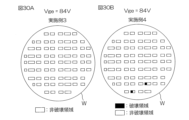
- the measurement targets were semiconductor devices 1 arranged at various locations on the surface of a circular wafer W.
- the applied voltage (V ge ) during the measurement was 80 V.
- the semiconductors measured were Examples 1 and 2 and Reference Examples 1 to 4.
- FIGS 26A to 26C and 27A to 27C The test results of the time-zero dielectric strength breakdown test are shown in Figures 26A to 26C and 27A to 27C.
- Figures 26A to 26C and 27A to 27C the parts of the wafer W where chips through which leakage currents larger than the reference value flow are present are shown as solid rectangles (destructive areas), and the parts of the wafer W where chips through which leakage currents smaller than the reference value flow are present are shown as open rectangles. In the chips present in the parts shown as solid rectangles, it is believed that the semiconductor device experienced dielectric breakdown during the time-zero dielectric strength breakdown test.
- Example 3 and 4> 1 to 3 were fabricated by the manufacturing process shown in Figures 14A to 22A and 14B to 22B.
- the processing time of the TCE treatment was 30 seconds (Example 3) and 45 seconds (Example 4), respectively.
- the third width W 3 of the first recess 96 (see Figure 8) and the fourth width W 4 of the second recess 97 (see Figure 10) were 1368 ⁇ .
- the third depth D3 (see FIG. 8) and the fourth depth D4 (see FIG. 10) are 1838 ⁇ .
- the processing time of the TCE processing is 45 seconds
- the third width W3 and the fourth width W4 are 2176 ⁇ .
- the third depth D3 and the fourth depth D4 are 2849 ⁇ .
- the graph in Fig. 28 is obtained as a relationship between the processing time of the TCE process and the amount of side etching of the trench. It can be seen from Fig. 28 that by increasing the processing time of the TCE process, the amount of side etching and the depth of the recess at the opening end of the trench also increase proportionally. In other words, by appropriately adjusting the processing time of the TCE process, the third width W3 and the third depth D3 of the first recess 96 and the fourth width W4 and the fourth depth D4 of the second recess 97 can be freely changed.
- the first width W 1 (see FIG. 8) of the isolation trench 21 is 1.0 ⁇ m
- the second width W 2 (see FIG. 10) of the gate trench 31 is 1.0 ⁇ m.
- the pitch P (see FIG. 6) is 15 ⁇ m.
- the width W 5 (see FIG. 4) of the mesa portion 90 is 10 ⁇ m.
- the third width W 3 of the first recess 96 (see FIG. 8 ) and the fourth width W 4 of the second recess 97 (see FIG. 10 ) were 532 ⁇ .
- the third depth D 3 (see FIG. 8 ) and the fourth depth D 4 (see FIG. 10 ) were 828 ⁇ .
- TZDB test time-zero dielectric breakdown test for measuring the time-zero dielectric breakdown resistance was carried out as a second breakdown test for Examples 3 and 4 and Reference Example 5.
- the applied voltage (Vge) was started from 78 V and gradually increased.
- breakdown started at an applied voltage Vge of 80 V, so no measurement was performed at voltages higher than this.
- TZDB test time-zero dielectric breakdown test
- 29A to 29C show the test results when the applied voltage Vge is 80 V.
- Figures 30A to 30C show the test results when the applied voltage Vge is 84 V.
- Figures 31A to 31C show the test results when the applied voltage Vge is 86 V.
- the IGBT structure Tr includes many T-shaped intersections 91P. Electric fields tend to concentrate at the T-shaped intersections 91P. As a result, the semiconductor chip 2 may be destroyed starting from the T-shaped intersections 91P. For this reason, the semiconductor device 1 is required to have high electrostatic discharge (ESD) resistance.
- ESD electrostatic discharge
- the electrostatic breakdown resistance tends to increase.
- a high electrostatic breakdown resistance is now required of the semiconductor device 1.
- the semiconductor device 1 is required to have not only a high electrostatic breakdown resistance but also a high dielectric breakdown.
- the curvature index CI P of the corner 92P of the T-shaped intersection 91P is 1.5 ⁇ m or more. Therefore, it is possible to reduce the occurrence of electric field concentration at the corner 92P of the T-shaped intersection 91P and to suppress the current concentration at the corner 92P of the T-shaped intersection 91P. This makes it possible to suppress the occurrence of breakdown at the T-shaped intersection 91P.
- the curvature index CI P of the corner 92P of the T-shaped intersection 91P is 2.4 ⁇ m or less. Therefore, the embeddability of the isolation buried electrode 23 in the isolation trench 21 and the embeddability of the gate buried electrode 33 in the gate trench 31 are not impaired. In other words, the occurrence of destruction at the T-shaped intersection 91P can be suppressed without impairing the embeddability of the buried electrodes 23, 33.
- the curvature index CI Q of the corner 92Q of the L-shaped intersection 91Q is 1.5 ⁇ m or more. This can reduce the occurrence of electric field concentration at the corner 92Q of the L-shaped intersection 91Q. This can prevent current from concentrating at the corner 92Q of the L-shaped intersection 91Q. This can prevent breakdown at the L-shaped intersection 91Q.
- the curvature index CIQ of the corner 92Q of the L-shaped intersection 91Q is 2.4 ⁇ m or less. Therefore, the embeddability of the isolated buried electrode 23 in the isolation trench 21 is not impaired. In other words, the occurrence of destruction at the L-shaped intersection 91Q can be suppressed without impairing the embeddability of the isolated buried electrode 23.
- the electrostatic breakdown resistance and dielectric breakdown resistance of the semiconductor device 1 can be improved. This makes it possible to avoid thickening of the gate insulating film 32, main surface insulating film 39, and interlayer insulating film 60 as a countermeasure against dielectric breakdown. As a result, the gate capacitance of the semiconductor device 1 can be reduced.
- the first recess 96 is formed at the opening ends 21d, 21e of the isolation trench 21. Since the third width W3 of the first recess 96 is 1350 ⁇ or more, it is possible to mitigate the occurrence of electric field concentration at the opening ends 21d, 21e of the isolation trench 21. Therefore, it is possible to suppress the current concentration at the opening ends 21d, 21e of the isolation trench 21. As a result, it is possible to suppress the occurrence of breakdown in the isolation trench 21.
- the third width W3 of the first recess 96 is 2000 ⁇ or less, it does not adversely affect the function of the isolation trench 21. In other words, it is possible to suppress the occurrence of breakdown in the isolation trench 21 without adversely affecting the function of the isolation trench 21.
- a second recess 97 is formed at the opening ends 31d, 31e of the gate trench 31. Since the fourth width W4 of the second recess 97 is 1350 ⁇ or more, it is possible to mitigate the occurrence of electric field concentration at the opening ends 31d, 31e of the gate trench 31. Therefore, it is possible to suppress the concentration of current at the opening ends 31d, 31e of the gate trench 31. This makes it possible to suppress the occurrence of breakdown at the opening ends 31d, 31e of the gate trench 31.
- the fourth width W4 of the second recess 97 is 2000 ⁇ or less, there is no adverse effect on the function of the gate trench 31. In other words, the occurrence of breakdown in the gate trench 31 can be suppressed without adversely affecting the function of the gate trench 31.
- the electrostatic breakdown resistance and dielectric breakdown resistance of the semiconductor device 1 can be further improved.
- the semiconductor device 1 was an IGBT discrete device in which an IGBT was mounted alone as a functional element, but it may also be an RC-IGBT (Reverse-Conducting Insulated Gate Bipolar Transistor) in which an IGBT and a diode are mixed.
- RC-IGBT Reverse-Conducting Insulated Gate Bipolar Transistor
- the IGBT structure Tr may include a cross-shaped intersection 91R where two trenches 202, 203 cross each other.
- the cross-shaped intersection 91R has four corners 92R.
- the curvature index CI R of each corner 92R may be 1.5 ⁇ m or more and 2.4 ⁇ m or less.
- a structure in which the conductivity type of each semiconductor portion is inverted may be adopted.
- the p-type portion may be formed as n-type
- the n-type portion may be formed as p-type.
- the IGBT structure (Tr) is A trench (21, 31) extending in multiple directions is formed on the first main surface (3) of the semiconductor chip (2); an insulating film (22, 32) formed on the side surface (21a, 21b, 31a, 31b) of the trench (21, 31); a buried conductor (23, 33) buried inside the trench (21, 31) via the insulating film (22, 32);
- the trenches (21, 31) extend in a plurality of directions, and the trenches (21, 31) intersect at the intersections (91P, 91Q, 91R),
- the semiconductor device (1, 201) has a curvature index (CIP, CIQ) of a corner (92P, 92Q) of the intersection (91P, 91Q, 91R) of 1.5
- the curvature index (CI P , CI Q ) of the corners (92P, 92Q) of the intersections (91P, 91Q, 91R) of the trenches (21, 31) is 1.5 ⁇ m or more, so that the occurrence of electric field concentration at the corners (92P, 92Q) of the trenches (21, 31) can be mitigated. Therefore, the concentration of current at the corners (92P, 92Q) of the trenches (21, 31) can be suppressed. This makes it possible to suppress the occurrence of breakdown in the trenches (21, 31). Therefore, the dielectric breakdown resistance can be improved.
- Appendix 1-2 The semiconductor device (1, 201) according to Appendix 1-1, wherein a chamfer width (W F ) of a virtual figure formed by extension lines (E1, E2) of two sides forming the corners (92P, 92Q) of the intersections (91P, 91Q, 91R) is 0.4 ⁇ m or more.
- the trenches (21, 31) extending in multiple directions include a first trench (21) and a plurality of second trenches (31) intersecting the first trench (21) at the intersections (91P, 91Q, 91R), the plurality of second trenches (31) being arranged in a stripe pattern spaced apart from one another;
- the semiconductor device (1, 201) according to any one of Appendices 1-1 to 1-5, wherein a ratio (CI P / P , CI Q /P) of the curvature index (CI P , CI Q ) of the corner portion (92P, 92Q) of the intersection portion (91P, 91Q, 91R) to a pitch (P) of the multiple second trenches (31) is 0.1 or more.
- the trenches (21, 31) extending in multiple directions include a first trench (21) and a plurality of second trenches (31) intersecting the first trench (21) at the intersections (91P, 91Q, 91R), the plurality of second trenches (31) being arranged in a stripe pattern spaced apart from one another;
- the semiconductor device (1, 201) according to any one of Appendices 1-1 to 1-7, wherein a ratio (CI P /W 5 , CI Q /W 5 ) of the curvature index (CI P , CI Q ) of the corner portion (92P, 92Q) of the intersection portion (91P, 91Q, 91R) to a width (W 5 ) of the mesa portion (90) defined between the plurality of second trenches (31) is 0.11 or more.
- the buried conductor (23, 33) includes a gate buried electrode (33) that controls a channel of the IGBT structure (Tr),
- the semiconductor device (1, 201) according to any one of Appendices 1-1 to 1-9, further comprising a drawn-out portion (40) that is integrally drawn out from the buried gate electrode (33) onto the first main surface (3) and covers the corner portions (92P, 92Q) of the intersection portions (91P, 91Q, 91R).
- the trenches (21, 31) extending in multiple directions are arranged in a stripe pattern spaced apart in a first direction, and include a plurality of gate trenches (31) each extending in a second direction, and a connection trench (21) extending in the first direction, connecting ends of the plurality of gate trenches (31) in the second direction to each other, and forming the T-shaped intersections (91P, 91Q, 91R) at connection portions with each of the gate trenches (31),
- the buried conductor (23, 33) is integrally buried in the gate trench (31) and the connection trench (21);
- the semiconductor device (1, 201) according to any one of Appendices 1-1 to 1-3, further comprising an extension portion (40) that is extended from the embedded conductor (23, 33) onto the first main surface (3) and covers the corner portions (92P, 92Q) of the intersection portions (91P, 91Q, 91R).
- the gate trench (31) and the connection trench (21) have equal widths;
- Appendix 1-16 The semiconductor device (1, 201) according to any one of Appendices 1-1 to 1-15, wherein the size of the semiconductor chip (2) is 0.5 mm square or more and 20 mm square or less.
- intersection portion (91P, 91Q, 91R) includes a T-shaped intersection portion (91P) where the trenches (21, 31) extending in the multiple directions intersect in a T shape.
- intersection portion (91P, 91Q, 91R) includes an L-shaped intersection portion (91Q) where the trenches (21, 31) extending in the multiple directions intersect in an L shape.
- intersection portion (91P, 91Q, 91R) includes a cross-shaped intersection portion (91R) where the trenches (21, 31) extending in the multiple directions intersect in a cross shape.
- the IGBT structure (Tr) is A trench (21, 31) formed in the first main surface (3) of the semiconductor chip (2); an insulating film (22, 32) formed on the side surface (21a, 21b, 31a, 31b) of the trench (21, 31); a buried conductor (23, 33) buried inside the trench (21, 31) via the insulating film (22, 32);
- a recess (96, 97) recessed toward a side surface (21a, 21b, 31a, 31b) of the trench (21, 31) is formed at an opening end (21d, 21e, 31d, 31e) of the trench (21, 31),
- recesses (96, 97) are formed at the opening ends (21d, 21e, 31d, 31e) of the trenches (21, 31). Since the widths ( W3 , W4 ) of the recesses (96, 97) are 1350 ⁇ or more, the occurrence of electric field concentration at the opening ends (21d, 21e, 31d, 31e) of the trenches (21, 31) can be mitigated. Therefore, the concentration of current at the opening ends (21d, 21e, 31d, 31e) of the trenches (21, 31) can be suppressed. This makes it possible to suppress the occurrence of breakdown in the trenches (21, 31). Therefore, the dielectric breakdown resistance can be improved.
- Appendix 2-2 The semiconductor device (1, 201) according to appendix 2-1, wherein the depth (D 3 , D 4 ) of the recess (96, 97) is 1850 ⁇ or more.
- Appendix 2-4 The semiconductor device ( 1 , 201) according to any one of Appendices 2-1 to 2-3 , wherein a ratio ( W3 / W1 , W4 / W2 ) of the width ( W3 , W4 ) of the recess (96, 97) to the width (W1, W2) of the trench (21, 31) is 0.14 or more.
- the trenches (31) are arranged in a stripe pattern at intervals from each other, The semiconductor device (1, 201) according to any one of Appendices 2-1 to 2-5, wherein a ratio (W 4 /P) of the width (W 4 ) of the recess (97) to the pitch ( P) of the plurality of trenches (31) is 0.009 or more.
- the trenches (31) are arranged in a stripe pattern at intervals from each other, The semiconductor device (1, 201) according to any one of Appendices 2-1 to 2-7, wherein a ratio (W 4 /W 5 ) of a width (W 4 ) of the recess (97) to a width (W 5 ) of a mesa portion (90) defined between the plurality of trenches (31) is 0.011 or more.
- the buried conductor (23, 33) includes a gate buried electrode (33) that controls a channel of the IGBT structure (Tr),
- the semiconductor device (1, 201) according to any one of Supplementary Notes 2-1 to 2-9, further comprising a drawn-out portion (40) that is integrally drawn out from the buried gate electrode (33) onto the first main surface (3) and covers the recesses (96, 97).
- the trenches (21, 31) are formed by a plurality of gate trenches (31) arranged in a stripe pattern at intervals in a first direction and each extending in a second direction, and a connection trench (21) extending in the first direction, connecting ends of the plurality of gate trenches (31) in the second direction to each other, and forming T-shaped intersections (91P, 91Q, 91R) at connection portions with each of the gate trenches (31);
- the recesses (96, 97) are formed at the intersections (91P, 91Q, 91R) of the trenches (21, 31),
- the buried conductor (23, 33) is integrally buried in the gate trench (31) and the connection trench (21);
- the semiconductor device (1, 201) according to any one of Appendices 2-1 to 2-3, further comprising an extension portion (40) that is extended from the embedded conductor (23, 33) onto the first main surface (3) and covers the recesses (96, 97) of the intersection
- the gate trench (31) and the connection trench (21) have equal widths;
- Appendix 2-20 The semiconductor device (1, 201) according to any one of Appendices 2-1 to 2-19, wherein the gate capacitance value of the semiconductor chip (2) is 300 pF or less.
Landscapes
- Electrodes Of Semiconductors (AREA)
Abstract
Description
本出願は、2023年3月9日に日本国特許庁に提出された特願2023-036385号に対応しており、この出願の全開示はここに引用により組み込まれるものとする。 This application corresponds to Patent Application No. 2023-036385 filed with the Japan Patent Office on March 9, 2023, the entire disclosure of which is incorporated herein by reference.
本開示は、トレンチ型のIGBT構造を備えた半導体装置に関する。 This disclosure relates to a semiconductor device with a trench-type IGBT structure.
特許文献1は、半導体装置の一例としてのRC-IGBT(Reverse Conducting - Insulated Gate Bipolar Transistor)を開示している。
本開示の一実施形態は、絶縁破壊耐量を向上できる、半導体装置を提供する。 One embodiment of the present disclosure provides a semiconductor device that can improve dielectric breakdown resistance.
本開示の一実施形態は、第1主面およびその反対側の第2主面を有する半導体チップと、前記半導体チップの前記第1主面に形成されたトレンチ型のIGBT構造とを含み、前記IGBT構造は、前記半導体チップの前記第1主面に形成されたトレンチと、前記トレンチの側面に形成された絶縁膜と、前記絶縁膜を介して前記トレンチの内側に埋め込まれた埋め込み導電体とを含み、前記トレンチの開口端に、前記トレンチの側面側に凹む凹部が形成されており、前記凹部の幅が、1350Å以上である、半導体装置を提供する。 One embodiment of the present disclosure provides a semiconductor device that includes a semiconductor chip having a first main surface and a second main surface opposite the first main surface, and a trench-type IGBT structure formed on the first main surface of the semiconductor chip, the IGBT structure including a trench formed on the first main surface of the semiconductor chip, an insulating film formed on a side surface of the trench, and an embedded conductor embedded inside the trench via the insulating film, and a recess is formed at the opening end of the trench that recesses into the side surface of the trench, and the width of the recess is 1350 Å or more.
本開示の一実施形態によれば、絶縁破壊耐量を向上できる半導体装置を提供できる。 According to one embodiment of the present disclosure, a semiconductor device can be provided that can improve the dielectric breakdown resistance.
図1は、本開示の一実施形態に係る半導体装置1の模式的な平面図である。図2は、複数のIGBT領域6、境界領域7、ゲート電極71およびエミッタ電極75のレイアウト例を示す平面図である。図3は、ゲート配線40、境界ウェル領域50および外周ウェル領域56のレイアウト例を示す平面図である。図4は、図2の一点鎖線IVで囲まれた部分の拡大図である。図5は、図4の一点鎖線Vで囲まれた部分の拡大図である。図6は、図4に示すVI-VI線に沿う断面図である。図7は、図4に示すVII-VII線に沿う断面図である。図8は、図6の一点鎖線VIIIで囲まれた部分の拡大図である。図9は、図5に示すIX-IX線に沿う断面図である。図10は、図7の一点鎖線Xで囲まれた部分の拡大図である。図11は、図2の一点鎖線XIで囲まれた部分の拡大図である。図12Aは、図11に示すXIIA-XIIA線に沿う断面図である。図12Bは、図11の一点鎖線XIIBで囲まれた部分の拡大図である。図13は、曲率指標CIを説明するための模式的な平面図である。
FIG. 1 is a schematic plan view of a
半導体装置1は、IGBT(Insulated Gate Bipolar Transistor)を備えたIGBT半導体装置である。
The
図1~図3に示すように、半導体装置1は、直方体形状の半導体チップ2を含む。半導体チップ2は、一方側の第1主面3、他方側の第2主面4、ならびに第1主面3および第2主面4を接続する側面5A,5B,5C,5Dを有している。第1主面3および第2主面4は、それらの法線方向Zから見た平面視(以下、単に「平面視」という。)において四角形状に形成されている。法線方向Zは、半導体チップ2の厚さ方向でもある。
As shown in Figures 1 to 3, the
第1側面5Aおよび第2側面5Bは、第1主面3に沿う第1方向Xに延び、第1方向Xに交差(具体的には直交)する第2方向Yに対向している。第3側面5Cおよび第4側面5Dは、第2方向Yに延び、第1方向Xに対向している。半導体チップ2は、シリコン単結晶基板からなる単層構造を有している。
The
半導体チップ2は、たとえば、平面視正方形状である。半導体チップ2のサイズは、たとえば、0.5mm角以上20mm角以下である。チップサイズが「Xmm角」とは、正方形状の半導体チップ2の一辺の長さがXmmであることを意味していてもよい。
The
図2および図3に示すように、半導体装置1は、第1主面3において第2方向Yに間隔を空けて形成された複数のIGBT領域6を含む。各IGBT領域6は、トレンチ型のIGBT構造(トランジスタ構造)Trを含む。IGBT領域6は「アクティブ領域」と称してもよい。複数のIGBT領域6は、第1IGBT領域6Aおよび第2IGBT領域6Bを含む。
As shown in Figures 2 and 3, the
図2および図3に示すように、第1IGBT領域6Aは、第1主面3の中心を第1方向Xに横切る直線に対して第1側面5A側の領域に形成されている。第2IGBT領域6Bは、第1主面3の中心を第1方向Xに横切る直線に対して第2側面5B側の領域に形成されている。複数のIGBT領域6は、この実施形態では、平面視において第1~第4側面5A~5Dに平行な四辺を有する四角環状にそれぞれ形成されている。
As shown in Figures 2 and 3, the
図2および図3に示すように、半導体装置1は、複数のIGBT領域6の間の領域に形成された境界領域7をさらに含む。具体的には、境界領域7は、第1IGBT領域6Aおよび第2IGBT領域6Bの間の領域において、第1方向Xに延びる帯状に設けられている。境界領域7は、図2および図3の例では、第1主面3の中心を第1方向Xに横切る直線上に位置している。
As shown in Figures 2 and 3, the
図2および図3に示すように、境界領域7は、第2方向Yに比較的大きい幅を有する第1境界領域8、および第1境界領域8よりも小さい幅を第2方向Yに有する第2境界領域9を含む。第1境界領域8は、端子電極を支持する部分として第1方向Xの一方側(第3側面5C側)の領域に設けられている。第1境界領域8は、「パッド領域」、「幅広領域」または「端子支持領域」と称してもよい。
As shown in Figures 2 and 3, the
第1境界領域8は、この実施形態では、平面視において第1主面3の中心を第1方向Xに横切る直線上に位置し、第3側面5Cの中央部近傍において四角形状に設けられている。第1境界領域8の幅は、100μm以上800μm以下であってもよい。第1境界領域8の幅は、200μm以上600μm以下であることが好ましい。第1境界領域8の幅は、この実施形態では、350μm以上450μm以下の範囲に設定されている。
In this embodiment, the
第2境界領域9は、配線を支持する部分として、第1境界領域8に対して第1方向Xの他方側(第4側面5D側)の領域に形成されている。第2境界領域9は、第1主面3の中心を第1方向Xに横切る直線上に位置し、第1境界領域8から第4側面5Dの中央部側に向けて帯状に引き出されている。第2境界領域9は、「ストリート領域」、「幅狭領域」または「配線支持領域」と称してもよい。
The
図2および図3に示すように、半導体装置1は、外周領域10をさらに含む。外周領域10は、複数のIGBT領域6を一括して取り囲む。外周領域10は、第1~第4側面5A~5Dに沿って延びる四角環状である。外周領域10は、境界領域7とともに、非活性領域(非アクティブ領域)を形成する。この実施形態では、境界領域7および外周領域10には、後述するIGBT構造Trは形成されていない。
As shown in Figures 2 and 3, the
図6、図7および図12Aに示すように、半導体装置1は、n型(第1導電型)のドリフト領域11を含む。ドリフト領域11は、半導体チップ2の内部の全域に形成されている。この実施形態では、半導体チップ2がn型の半導体基板からなり、この半導体基板を利用してドリフト領域11が形成されている。
As shown in Figures 6, 7 and 12A, the
図6、図7および図12Aに示すように、半導体装置1は、第2主面4の表層部に形成されたn型のバッファ領域12をさらに含む。バッファ領域12は、この実施形態では、第2主面4の全域において第2主面4に沿って延びる層状に形成されている。バッファ領域12は、ドリフト領域11よりも高いn型不純物濃度を有している。バッファ領域12の有無は任意であり、バッファ領域12を有さない形態が採用されてもよい。
As shown in Figures 6, 7 and 12A, the
図6、図7および図12Aに示すように、半導体装置1は、第2主面4の表層部に形成されたp型(第2導電型)のコレクタ領域13を含む。コレクタ領域13は、この実施形態では、バッファ領域12の第2主面4側の表層部に形成されている。コレクタ領域13は、この実施形態では、第2主面4の全域において第2主面4に沿って延びる層状に形成されている。コレクタ領域13は、第2主面4および第1~第4側面5A~5Dの一部から露出している。
As shown in Figures 6, 7 and 12A, the
図2および図4に示すように、半導体装置1は、複数のIGBT領域6を区画するように第1主面3に形成された複数のトレンチ分離構造20をさらに含む。複数のトレンチ分離構造20には、ゲート電位が印加される。トレンチ分離構造20は、「トレンチゲート分離構造」または「トレンチゲート接続構造」と称してもよい。複数のトレンチ分離構造20は、第1トレンチ分離構造20A、および第2トレンチ分離構造20Bを含む。
As shown in Figures 2 and 4, the
図2および図4に示すように、第1トレンチ分離構造20Aは、第1IGBT領域6Aを取り囲み、境界領域7および外周領域10から第1IGBT領域6Aを区画している。第1トレンチ分離構造20Aは、この実施形態では、平面視において半導体チップ2の周縁に平行な四辺を有する多角環状に形成されている。第1トレンチ分離構造20Aは、平面視において境界領域7の第1境界領域8および第2境界領域9を区画するように屈曲した部分を有している。
As shown in Figures 2 and 4, the first
図2および図4に示すように、第2トレンチ分離構造20Bは、第2IGBT領域6Bを取り囲み、境界領域7および外周領域10から第2IGBT領域6Bを区画している。第2トレンチ分離構造20Bは、この実施形態では、平面視において半導体チップ2の周縁に平行な四辺を有する多角環状に形成されている。第2トレンチ分離構造20Bは、平面視において境界領域7の第1境界領域8および第2境界領域9を区画するように屈曲した部分を有している。
As shown in Figures 2 and 4, the second
図2、図4および図11に示すように、各トレンチ分離構造20A,20Bは、第1方向Xに延びる少なくとも2つの第1方向部20X、および第2方向Yに延びる少なくとも2つの第2方向部20Yを含む。第1方向部20Xの端部および第2方向部20Yの端部は、機械的および電気的に接続されている。第1方向部20Xの端部と第2方向部20Yの端部とがL字形状に交差し、多角環状のトレンチ分離構造20A,20Bの角部を形成している。
As shown in Figures 2, 4 and 11, each
以下、1つのトレンチ分離構造20の構成が説明される。トレンチ分離構造20の説明において、図8および図9は、いずれもトレンチ分離構造20の断面を示している。図8が、トレンチ分離構造20の長手方向に直交する方向の断面であり、図9が、トレンチ分離構造20のT字状交差部91P(後述する)を横切る方向の断面である。
Below, the configuration of one
図7~図9に示すように、トレンチ分離構造20は、分離トレンチ21(第1トレンチ)、分離絶縁膜22および分離埋め込み電極(埋め込み導電体)23を含む。分離トレンチ21は、第1主面3から第2主面4に向けて掘り下がり、トレンチ分離構造20の壁面を区画している。
As shown in Figures 7 to 9, the
分離トレンチ21は、第1主面3に形成されている。分離トレンチ21は、断面視において垂直形状に形成されている。分離トレンチ21は、互いに対向する一対の側面21a,21bと、一対の側面21a,21bを接続する底面21cとを含む。底面21cは、断面視において第2主面4側に膨らむラウンド形状を有している。
The
図8に示すように、分離トレンチ21は、第1幅W1を有している。第1幅W1は、分離トレンチ21が延びる方向に直交する方向の幅(最大値)である。第1幅W1は、第2境界領域9の幅未満の幅であることが好ましい。第1幅W1は、0.5μm以上2.0μm以下であることが好ましい。より具体的には、第1幅W1は、1.0μmであってもよい。
8, the
分離トレンチ21は、第1深さD1を有している。第1深さD1は、1μm以上30μm以下であってもよい。第1深さD1は、4μm以上15μm以下であることが好ましい。第1深さD1は、6μm以上10μm以下であることが特に好ましい。分離トレンチ21が、断面視において第2主面4に向かって幅が小さくなるテーパ形状に形成されていてもよい。底面21cが、第1主面3に平行な平坦面であってもよい。
The
図8および図9に示すように、分離トレンチ21の開口端21d,21eには、分離トレンチ21の側面21a,21b側に凹む第1凹部96が形成されている。第1凹部96の断面形状は、分離トレンチ21の側面21a,21b側に向けて窪んだ弧状である。第1凹部96は、第3幅W3を有している。第3幅W3は、側面21a,21bの延長線と第1主面3とが交差する地点と第1凹部96の端部との間の第2方向Yの幅である。第3幅W3は、1350Å以上であり2000Å以下である。第1凹部96は、第3深さD3を有している。第3深さD3は、第3幅W3よりも大きい。第3深さD3は、1850Å以上である。分離トレンチ21の第1幅W1に対する第3幅W3の比(W3/W1)が、0.14以上0.2以下である。
As shown in FIG. 8 and FIG. 9, a
図7~図9に示すように、分離絶縁膜22は、分離トレンチ21の側面21a,21bに沿って膜状に形成されている。分離絶縁膜22は、分離トレンチ21内においてリセス空間を区画している。分離絶縁膜22は、酸化シリコン膜、窒化シリコン膜、酸窒化シリコン膜および酸化アルミニウム膜のうちの少なくとも一つを含んでいてもよい。分離絶縁膜22は、単一の絶縁膜からなる単層構造を有していることが好ましい。分離絶縁膜22は、半導体チップ2の酸化物からなる酸化シリコン膜を含むことが特に好ましい。
As shown in Figures 7 to 9, the
図7~図9に示すように、分離埋め込み電極23は、分離絶縁膜22を挟んで分離トレンチ21内に埋め込まれている。分離埋め込み電極23は、この実施形態では、導電性ポリシリコンからなる。分離埋め込み電極23には、ゲート電位が付与される。
As shown in Figures 7 to 9, the isolated buried
以下、複数のIGBT領域6内の構造が説明される。第2IGBT領域6B側の構造は、第1IGBT領域6A側の構造とほぼ同じである。具体的には、第2IGBT領域6B側の構造は、第1IGBT領域6A側の構造と、境界領域7に対して線対称である。以下では、第1IGBT領域6A側の構造が説明される。第2IGBT領域6B側の構造の説明については、第1IGBT領域6A側の構造の説明が適用され、省略される。
Below, the structure within the
図6および図7に示すように、半導体装置1は、第1IGBT領域6Aにおいて第1主面3の表層部に形成されたp型のベース領域25を含む。ベース領域25は、「ボディ領域」または「チャネル領域」と称してもよい。ベース領域25は、トレンチ分離構造20よりも浅い深さ位置に形成され、トレンチ分離構造20の底壁よりも第1主面3側に位置する底部を有している。ベース領域25は、第1主面3に沿って層状に延び、トレンチ分離構造20の内周壁に接続されている。
As shown in Figures 6 and 7, the
図2および図4に示すように、半導体装置1は、複数のトレンチ構造30を含む。複数のトレンチ構造30には、ゲート電位が印加される。複数のトレンチ構造30は、ベース領域25を貫通して、ドリフト領域11に達している。複数のトレンチ構造30は、平面視において第1方向Xに間隔を空けて配列され、第2方向Yに延びる帯状にそれぞれ形成されている。つまり、複数のトレンチ構造30は、第2方向Yに延びるストライプ状に配列されている。
As shown in Figures 2 and 4, the
図4および図11に示すように、複数のトレンチ構造30は、長手方向(第2方向Y)に関して、境界領域7側の第1端部30Aおよび外周領域10側の第2端部30Bをそれぞれ有している。第1端部30Aおよび第2端部30Bは、トレンチ分離構造20に機械的および電気的に接続されている。つまり、複数のトレンチ構造30は、トレンチ分離構造20と共に1つの梯子状のトレンチゲート構造を構成している。トレンチ構造30およびトレンチ分離構造20の接続部は、トレンチ分離構造20の一部とみなされてもよいし、トレンチ構造30の一部とみなされてもよい。
As shown in Figures 4 and 11, the
以下、1つのトレンチ構造30の構成が説明される。
The configuration of one
図6および図10に示すように、トレンチ構造30は、ゲートトレンチ31(第2トレンチ)、ゲート絶縁膜32およびゲート埋め込み電極(埋め込み導電体)33を含む。ゲートトレンチ31は、第1主面3から第2主面4に向けて掘り下がり、トレンチ構造30の壁面を区画している。
As shown in Figures 6 and 10, the
ゲートトレンチ31は、第1主面3に形成されている。ゲートトレンチ31は、断面視において垂直形状に形成されている。ゲートトレンチ31は、互いに対向する一対の側面31a,31bと、一対の側面31a,31bを接続する底面31cとを含む。底面31cは、断面視において第2主面4側に膨らむラウンド形状を有している。ゲートトレンチ31は、この実施形態では、第2方向Yの両端部(第1端部30Aおよび第2端部30B)において分離トレンチ21に連通している。具体的には、ゲートトレンチ31の側壁は分離トレンチ21の側壁に連通し、ゲートトレンチ31の底壁は分離トレンチ21の底壁に連通している。
The
図6に示すように、複数のゲートトレンチ31は、第1方向Xに一定のピッチPを空けて配列されている。複数のゲートトレンチ31のピッチPは、境界領域7の第2境界領域9の幅未満であることが好ましい。複数のゲートトレンチ31のピッチPは、5μm以上30μm以下であってもよい。複数のゲートトレンチ31のピッチPは、10μm以上20μm以下であることが好ましい。複数のゲートトレンチ31のピッチPは、15μmであることが好ましい。
As shown in FIG. 6, the
図10に示すように、ゲートトレンチ31は、第2幅W2を有している。第2幅W2は、ゲートトレンチ31が延びる方向に直交する方向の幅(最大値)である。第2幅W2は、0.5μm以上2.0μm以下であることが好ましい。より具体的には、第2幅W2は、1.0μmであってもよい。第2幅W2が、第1幅W1とほぼ等しくてもよい。
10, the
図10に示すように、ゲートトレンチ31は、第2深さD2を有している。第2深さD2は、1μm以上30μm以下であってもよい。第2深さD2は、4μm以上15μm以下であることが好ましい。第2深さD2は、6μm以上10μm以下であることが特に好ましい。第2深さD2は、第1深さD1と、ほぼ等しいことが好ましい。ゲートトレンチ31が、断面視において第2主面4に向かって幅が小さくなるテーパ形状に形成されていてもよい。底面31cが、第1主面3に平行な平坦面であってもよい。
10, the
図10に示すように、ゲートトレンチ31の開口端31d,31eには、ゲートトレンチ31の側面31a,31b側に凹む第2凹部97が形成されている。第2凹部97の断面形状は、ゲートトレンチ31の側面31a,31b側に向けて窪んだ弧状である。第2凹部97は、第4幅W4を有している。第4幅W4は、側面31a,31bの延長線と第1主面3とが交差する地点と第2凹部97の端部との間の第1方向Xの幅である。第4幅W4は、1350Å以上であり2000Å以下である。第2凹部97は、第4深さD4を有している。第4深さD4は、第4幅W4よりも大きい。第4深さD4は、1850Å以上である。ゲートトレンチ31の第2幅W2に対する第4幅W4の比(W4/W2)が、0.14以上0.2以下である。複数のゲートトレンチ31のピッチP(後述する)に対する第4幅W4の比(W4/P)が、0.009以上0.0133以下である。メサ部90(後述する)の第5幅W5(後述する)に対する第4幅W4の比(W4/W5)が、0.011以上0.017以下である。
As shown in FIG. 10, a
図6および図10に示すように、ゲート絶縁膜32は、ゲートトレンチ31の壁面に沿って膜状に形成されている。ゲート絶縁膜32は、ゲートトレンチ31内においてリセス空間を区画している。ゲート絶縁膜32の厚さは、たとえば、50nm以上200nm以下である。
As shown in FIG. 6 and FIG. 10, the
ゲート絶縁膜32は、酸化シリコン膜、窒化シリコン膜、酸窒化シリコン膜および酸化アルミニウム膜のうちの少なくとも一つ1つを含んでいてもよい。ゲート絶縁膜32は、単一の絶縁膜からなる単層構造を有していることが好ましい。ゲート絶縁膜32は、半導体チップ2の酸化物からなる酸化シリコン膜を含むことが特に好ましい。ゲート絶縁膜32は、この実施形態では、分離絶縁膜22と同一の絶縁膜からなる。ゲート絶縁膜32は、分離トレンチ21およびゲートトレンチ31の連通部において分離絶縁膜22に接続されている。
The
図6および図10に示すように、ゲート埋め込み電極33は、ゲート絶縁膜32を挟んでゲートトレンチ31内に埋め込まれている。ゲート埋め込み電極33は、この実施形態では、導電性ポリシリコンからなる。ゲート埋め込み電極33には、ゲート電位が付与される。ゲート埋め込み電極33は、分離トレンチ21およびゲートトレンチ31の連通部において分離埋め込み電極23に接続されている。
As shown in FIG. 6 and FIG. 10, the gate buried
図4および図6に示すように、半導体装置1は、ベース領域25の表層部に形成されたn型の複数のエミッタ領域35をさらに含む。複数のエミッタ領域35は、ドリフト領域11よりも高いn型不純物濃度をそれぞれ有している。複数のエミッタ領域35は、複数のトレンチ構造30の両サイドにそれぞれ形成されている。複数のエミッタ領域35は、平面視において複数のトレンチ構造30に沿って延びる帯状にそれぞれ形成されている。むろん、複数のエミッタ領域35は、平面視において複数のトレンチ構造30に沿って間隔を空けて形成されていてもよい。
As shown in Figures 4 and 6, the
図6に示すように、半導体装置1は、半導体チップ2内においてベース領域25の直下の領域に形成されたn型の複数のキャリアストレージ領域36をさらに含む。複数のキャリアストレージ領域36は、ベース領域25へのキャリア(正孔)の排出を抑制し、複数のトレンチ構造30の直下の領域におけるキャリア(正孔)の蓄積を促す。つまり、複数のキャリアストレージ領域36は、半導体チップ2の内部から低オン抵抗化および低オン電圧化を促す。
As shown in FIG. 6, the
複数のキャリアストレージ領域36は、複数のトレンチ構造30の両サイドに配置され、平面視において複数のトレンチ構造30に沿って延びる帯状にそれぞれ形成されている。複数のキャリアストレージ領域36は、半導体チップ2の厚さ方向に関してベース領域25の底部およびトレンチ構造30の底壁の間の領域にそれぞれ形成されている。複数のキャリアストレージ領域36は、トレンチ構造30の底壁からベース領域25側に離間していることが好ましい。複数のキャリアストレージ領域36の底部は、トレンチ構造30の中間部よりもトレンチ構造30の底壁側に位置していることが好ましい。複数のキャリアストレージ領域36は、ドリフト領域11よりも高いn型不純物濃度を有している。複数のキャリアストレージ領域36のn型不純物濃度は、エミッタ領域35よりも低いことが好ましい。キャリアストレージ領域36の有無は任意である。したがって、キャリアストレージ領域36を有さない形態が採用されてもよい。
The
図6に示すように、半導体装置1は、エミッタ領域35を露出させるように第1主面3に形成された複数のコンタクト孔37を含む。複数のコンタクト孔37は、複数のトレンチ構造30から第1方向Xに間隔を空けて複数のトレンチ構造30の両サイドに形成されている。複数のコンタクト孔37は、図6に示すように、開口から底壁に向けて開口幅が狭まる先細り形状にそれぞれ形成されていてもよい。
As shown in FIG. 6, the
図6に示すように、複数のコンタクト孔37は、ベース領域25に至らないようにエミッタ領域35の底部から第1主面3側に離間していてもよい。むろん、複数のコンタクト孔37は、ベース領域25に至るようにエミッタ領域35を貫通していてもよい。複数のコンタクト孔37は、平面視において複数のトレンチ構造30に沿って延びる帯状にそれぞれ形成されている。長手方向(第2方向Y)に関して、複数のコンタクト孔37は、複数のトレンチ構造30よりも短い。
As shown in FIG. 6, the multiple contact holes 37 may be spaced from the bottom of the
図6に示すように、半導体装置1は、ベース領域25の表層部において複数のエミッタ領域35とは異なる領域に形成されたp型の複数のコンタクト領域38を含む。複数のコンタクト領域38は、平面視において対応するコンタクト孔37に沿って延びる帯状にそれぞれ形成されている。複数のコンタクト領域38の底部は、対応するコンタクト孔37の底壁およびベース領域25の底部の間の領域にそれぞれ形成されている。複数のコンタクト領域38は、ベース領域25よりも高いp型不純物濃度を有している。
As shown in FIG. 6, the
このように、ベース領域25、複数のトレンチ構造30、複数のエミッタ領域35、複数のキャリアストレージ領域36、複数のコンタクト孔37および複数のコンタクト領域38が、IGBT構造Tr(図2および図4参照)に含まれる。
In this way, the
図4に示すように、半導体装置1は、第1IGBT領域6Aにおいて区画された複数のメサ部90を含む。複数のメサ部90は、ゲートトレンチ31によって区画されている。各メサ部90は、第1方向Xに隣り合う一対のゲートトレンチ31の間の領域に区画されている。メサ部90は、半導体チップ2の一部からなる。複数のメサ部90は、第2方向Yに延びる帯状にそれぞれ延び、第1方向Xに間隔を空けて区画されている。つまり、複数のメサ部90は、第2方向Yに延びるストライプ状に形成されている。
As shown in FIG. 4, the
図4に示すように、メサ部90は、第5幅W5を有している。第5幅W5は、メサ部90が延びる方向に直交する方向の幅(最大値)である。第5幅W5は、第2境界領域9の幅未満の幅であることが好ましい。第5幅W5は、11μm以上21μm以下であってもよい。11μm以上16μm以下であることが好ましい。第5幅W5は、14μmであることが好ましい。
As shown in Fig. 4, the
図3および図4に示すように、半導体装置1は、境界領域7において第1主面3の表層部に形成されたp型の境界ウェル領域50を含む。境界ウェル領域50は、この実施形態では、複数のベース領域25よりも高いp型不純物濃度を有している。むろん、境界ウェル領域50は、複数のベース領域25よりも低いp型不純物濃度を有していてもよい。境界ウェル領域50は、第1トレンチ分離構造20Aおよび第2トレンチ分離構造20Bによって挟まれた領域に形成されている。境界ウェル領域50は、平面視において境界領域7に沿って第1方向Xに延びている。
As shown in Figures 3 and 4, the
図3に示すように、境界ウェル領域50は、境界領域7の第1境界領域8に形成された第1境界ウェル領域51、および境界領域7の第2境界領域9に形成された第2境界ウェル領域52を含む。第1境界ウェル領域51は、第2方向Yに比較的大きい領域幅を有している。第1境界ウェル領域51は、平面視において四角形状に形成されている。第1境界ウェル領域51は、第1境界領域8の全域に形成されていることが好ましい。
As shown in FIG. 3, the
図3および図4に示すように、第2境界ウェル領域52は、第2方向Yに第1境界ウェル領域51の領域幅よりも小さい領域幅を有し、第1境界ウェル領域51から第2境界領域9に向けて帯状に引き出されている。第2境界ウェル領域52は、この実施形態では、第1主面3の中心を第1方向Xに横切る直線上に位置している。
As shown in Figures 3 and 4, the second
図7に示すように、境界ウェル領域50は、ベース領域25よりも深く形成されている。境界ウェル領域50は、複数のトレンチ分離構造20よりも深く形成されていることが好ましい。図4に示すように、境界ウェル領域50は、この実施形態では、第2方向Yに境界領域7の幅よりも大きい幅を有し、境界領域7から複数のIGBT領域6内に引き出されている。
As shown in FIG. 7, the
図7に示すように、境界ウェル領域50は、第2方向Yに隣り合う複数のトレンチ分離構造20に接続されている。境界ウェル領域50は、複数のトレンチ分離構造20の底壁を被覆する部分を有している。境界ウェル領域50は、複数のトレンチ分離構造20を横切って複数のトレンチ構造30の底壁を被覆する部分を有している。
As shown in FIG. 7, the
図7に示すように、境界ウェル領域50は、各IGBT領域6内においてトレンチ分離構造20の側壁を被覆している。図示を省略するが、境界ウェル領域50は、各IGBT領域6内において複数のトレンチ構造30の側壁を被覆している。図4および図7に示すように、境界ウェル領域50は、第1主面3の表層部において各ベース領域25に接続されている。
As shown in FIG. 7, the
図3および図11に示すように、半導体装置1は、外周領域10において第1主面3の表層部に形成されたp型の外周ウェル領域56を含む。外周ウェル領域56は、この実施形態では、複数のベース領域25よりも高いp型不純物濃度を有している。むろん、外周ウェル領域56は、複数のベース領域25よりも低いp型不純物濃度を有していてもよい。外周ウェル領域56のp型不純物濃度は、境界ウェル領域50のp型不純物濃度とほぼ等しいことが好ましい。
As shown in Figures 3 and 11, the
図3および図12Aに示すように、外周ウェル領域56は、第1主面3に沿って延びる層状に形成され、第1主面3から露出している。外周ウェル領域56は、第1主面3の周縁(第1~第4側面5A~5D)から内方に間隔を空けて形成されている。外周ウェル領域56は、平面視において複数のIGBT領域6に沿って延びる帯状に形成されている。外周ウェル領域56は、この実施形態では、平面視において複数のIGBT領域6を取り囲む環状に形成されている。具体的には、外周ウェル領域56は、第1主面3の周縁に平行な四辺を有する四角環状に形成されている。
As shown in Figures 3 and 12A, the
図12Aに示すように、外周ウェル領域56は、複数のベース領域25よりも深く形成されている。外周ウェル領域56は、複数のトレンチ分離構造20(複数のトレンチ構造30)よりも深く形成されていることが特に好ましい。外周ウェル領域56は、この実施形態では、境界ウェル領域50とほぼ等しい深さを有している。
As shown in FIG. 12A, the
図12Aに示すように、外周ウェル領域56は、複数のトレンチ分離構造20に接続されている。外周ウェル領域56は、複数のトレンチ分離構造20の底壁を被覆する部分を有している。外周ウェル領域56は、外周領域10から各IGBT領域6(図3参照)内に引き出されている。外周ウェル領域56は、複数のトレンチ分離構造20を横切って複数のトレンチ構造30の底壁を被覆する部分を有している。
As shown in FIG. 12A, the
図4および図11に示すように、IGBT構造Trは、トレンチ分離構造20とトレンチ構造30との接続部分に形成されるT字状交差部91Pを複数含む。複数のT字状交差部91Pは、トレンチ構造30の第1端部30Aとトレンチ分離構造20の境界領域7側の第1方向部20Xとの接続部分に形成される複数の第1T字状交差部91PA(図4)と、トレンチ構造30の第2端部30Bとトレンチ分離構造20の外周領域10側の第1方向部20Xとの接続部分に形成される複数の第2T字状交差部91PB(図11)とを含む。
As shown in FIG. 4 and FIG. 11, the IGBT structure Tr includes a plurality of T-shaped
図4に示すように、複数の第1T字状交差部91PAは、半導体チップ2の厚さ方向に境界配線42および境界ウェル領域50(第2境界ウェル領域52)に対向している。図11に示すように、複数の第2T字状交差部91PBは、第1外周配線43および外周ウェル領域56に、半導体チップ2の厚さ方向に対向している。
As shown in FIG. 4, the first T-shaped intersections 91PA face the
図5に示すように、T字状交差部91Pは、2つの角部92Pを有している。各角部92Pの曲率指標CIPは、1.5μm以上2.4μmである。曲率指標CIPは、角部92Pの曲率指標CI(図13参照)である。
5, the T-shaped
図13に示すように、曲率指標CIは、角部(角部92P、角部92Q)の曲率を定義するための指標である。角部(角部92P、角部92Q)は、第1辺93と第2辺94とによって形成されている。具体的には、曲率指標CIは、角部(角部92P、角部92Q)を形成する第1辺93の延長線E1と、延長線E1に直交し、角部(角部92P、角部92Q)を形成する第2辺94の延長線E2との交点P1と、角部(角部92P、角部92Q)との間の最短距離である。別の言い方では、延長線E1および延長線E2の双方に45°に交差する角部(角部92P、角部92Q)の接線TLと、交点P1との最短距離である。
As shown in FIG. 13, the curvature index CI is an index for defining the curvature of the corners (
T字状交差部91Pにおいて、角部92Pの曲率指標CIPの、分離トレンチ21の第1幅W1に対する比(CIP/W1)が、1.5以上2.4以下である。T字状交差部91Pにおいて、角部92Pの曲率指標CIPの、複数のゲートトレンチ31の第2幅W2に対する比(CIP/W2)が、1.5以上2.4以下である。T字状交差部91Pにおいて、角部92Pの曲率指標CIPの、複数のゲートトレンチ31のピッチPに対する比(CIP/P)が、0.1以上0.16以下である。T字状交差部91Pにおいて、角部92Pの曲率指標CIPの、メサ部90の第5幅W5に対する比(CIP/W5)が、0.11以上0.17以下である。
At the T-shaped
図11に示すように、IGBT構造Trは、トレンチ分離構造20の第1方向部20Xと、トレンチ分離構造20の第2方向部20Yとの接続部分に形成されるL字状交差部91Qを複数含む。複数のL字状交差部91Qは、トレンチ分離構造20の境界領域7側の第1方向部20Xと第2方向部20Yとの接続部分に形成される複数の第1L字状交差部91(図示せず)と、トレンチ分離構造20の外周領域10側の第1方向部20Xと第2方向部20Yとの接続部分に形成される複数の第2L字状交差部91QBとを含む。
11, the IGBT structure Tr includes a plurality of L-shaped
複数の第1L字状交差部91(図示せず)は、半導体チップ2の厚さ方向に境界配線42および境界ウェル領域50(第2境界ウェル領域52)に対向している。複数の第2L字状交差部91QBは、第1外周配線43および外周ウェル領域56に、半導体チップ2の厚さ方向に対向している。
The multiple first L-shaped intersections 91 (not shown) face the
図12Bに示すように、L字状交差部91Qは、1つの角部92Qを有している。角部92Qの曲率指標は、1.5μm以上2.4μmである。曲率指標CIPは、角部92Qの曲率指標CI(図13参照)である。
12B, the L-shaped
L字状交差部91Qにおいて、角部92Qの曲率指標CIQの、分離トレンチ21の第1幅W1に対する比(CIQ/W1)が、1.5以上2.4以下である。L字状交差部91Qにおいて、角部92Qの曲率指標CIQの、複数のゲートトレンチ31の第2幅W2に対する比(CIQ/W2)が、1.5以上2.4以下である。L字状交差部91Qにおいて、角部92Pの曲率指標CIQの、複数のゲートトレンチ31のピッチPに対する比(CIQ/P)が、0.1以上0.16以下である。L字状交差部91Qにおいて、角部92Qの曲率指標CIQの、メサ部90の第5幅W5に対する比(CIQ/W5)が、0.11以上0.17以下である。
At the L-shaped
図6、図7および図12Aに示すように、半導体装置1は、第1主面3を被覆する主面絶縁膜39を含む。主面絶縁膜39の厚さは、たとえば、50nm以上200nm以下である。
As shown in Figures 6, 7, and 12A, the
主面絶縁膜39は、酸化シリコン膜、窒化シリコン膜、酸窒化シリコン膜および酸化アルミニウム膜のうちの少なくとも一つを含んでいてもよい。主面絶縁膜39は、単一の絶縁膜からなる単層構造を有していることが好ましい。主面絶縁膜39は、半導体チップ2の酸化物からなる酸化シリコン膜を含むことが特に好ましい。主面絶縁膜39は、この実施形態では、ゲート絶縁膜32と同一の絶縁膜からなる。
The main
図6、図7および図12Aに示すように、主面絶縁膜39は、複数のIGBT領域6、境界領域7および外周領域10を被覆するように第1主面3に沿って膜状に延びている。主面絶縁膜39は、半導体チップ2の周縁(第1~第4側面5A~5D)に連なっていてもよい。
As shown in Figures 6, 7 and 12A, the main
図6および図7に示すように、主面絶縁膜39は、複数のトレンチ分離構造20および複数のトレンチ構造30を露出させるように第1主面3を被覆している。具体的には、主面絶縁膜39は、分離絶縁膜22およびゲート絶縁膜32に接続され、分離埋め込み電極23およびゲート埋め込み電極33を露出させている。
As shown in Figures 6 and 7, the main
図7に示すように、半導体装置1は、半導体チップ2の第1主面3の上に配置されたゲート配線40を含む。具体的には、ゲート配線40は、主面絶縁膜39の上に膜状に配置されている。ゲート配線40は、この実施形態では、導電性ポリシリコン膜からなる。
As shown in FIG. 7, the
図3に示すように、ゲート配線40は、少なくとも境界領域7に引き回されている。ゲート配線40は、この実施形態では、境界領域7および外周領域10に任意のレイアウトで引き回されている。具体的には、ゲート配線40は、パッド配線41、境界配線42、第1外周配線43および第2外周配線44を含む。パッド配線41は、境界領域7の第1境界領域8の上に配置され、第2方向Yに比較的大きい第1配線幅を有している。パッド配線41は、この実施形態では、平面視において四角形状に形成されている。パッド配線41は、第2方向Yに境界領域7の幅(第1境界領域8の幅)よりも大きい幅を有している。パッド配線41は、境界領域7の上から第2方向Yに隣り合う複数のトレンチ分離構造20の上に引き出されている。
As shown in FIG. 3, the
図3に示すように、パッド配線41は、この実施形態では、境界領域7の上から複数のIGBT領域6の上に引き出されている。これにより、パッド配線41は、分離埋め込み電極23および複数のゲート埋め込み電極33に機械的および電気的に接続され、分離埋め込み電極23およびゲート埋め込み電極33にゲート電位を伝達する。パッド配線41は、この実施形態では、分離埋め込み電極23および複数のゲート埋め込み電極33と一体的に形成されている。
As shown in FIG. 3, in this embodiment, the
図3および図4に示すように、境界配線42は、パッド配線41から境界領域7の第2境界領域9の上に引き出され、第2方向Yにパッド配線41の第1配線幅よりも小さい第2配線幅を有している。境界配線42は、第1方向Xに延びる帯状に形成されている。境界配線42は、この実施形態では、半導体チップ2の中心を横切っている。境界配線42は、第2方向Yに境界領域7の幅(第2境界領域9の幅)よりも大きい幅を有している。境界配線42は、境界領域7の上から第2方向Yに隣り合う複数のトレンチ分離構造20の上に引き出されている。
As shown in Figures 3 and 4, the
図4に示すように、境界配線42は、この実施形態では、複数のトレンチ構造30の第1端部30Aを被覆するように境界領域7の上から複数のIGBT領域6の上に引き出されている。これにより、境界配線42は、分離埋め込み電極23および複数のゲート埋め込み電極33に機械的および電気的に接続され、分離埋め込み電極23およびゲート埋め込み電極33にゲート電位を伝達する。境界配線42は、この実施形態では、分離埋め込み電極23および複数のゲート埋め込み電極33と一体的に形成されている。
As shown in FIG. 4, in this embodiment, the
図3に示すように、第1外周配線43は、パッド配線41から外周領域10の上に引き出され、第1側面5Aおよび第3側面5Cに沿って延びる帯状に形成されている。第1外周配線43は、第4側面5Dに沿って帯状に延びる部分を有していてもよい。第1外周配線43は、第1側面5Aに沿って延びる部分において外周領域10の上から第1トレンチ分離構造20Aの上に引き出された部分を有している。図11に示すように、第1外周配線43は、この実施形態では、第1IGBT領域6Aの複数のトレンチ構造30の第2端部30Bも被覆している。
As shown in FIG. 3, the first
これにより、第1外周配線43は、分離埋め込み電極23および複数のゲート埋め込み電極33に機械的および電気的に接続されている。第1外周配線43は、この実施形態では、分離埋め込み電極23および複数のゲート埋め込み電極33と一体的に形成されている。第1外周配線43は、外周領域10側から分離埋め込み電極23およびゲート埋め込み電極33にゲート電位を伝達する。
As a result, the first
図3に示すように、第2外周配線44は、パッド配線41から外周領域10の上に引き出され、第2側面5Bおよび第3側面5Cに沿って延びる帯状に形成されている。第2外周配線44は、第4側面5Dに沿って帯状に延びる部分を有していてもよい。第2外周配線44は、第2側面5Bに沿って延びる部分において外周領域10の上から第2トレンチ分離構造20Bの上に引き出された部分を有している。図示を省略するが、第2外周配線44は、この実施形態では、第2IGBT領域6Bの複数のトレンチ構造30の第2端部30Bも被覆している。
As shown in FIG. 3, the second
これにより、第2外周配線44は、分離埋め込み電極23および複数のゲート埋め込み電極33に機械的および電気的に接続されている。第2外周配線44は、この実施形態では、分離埋め込み電極23および複数のゲート埋め込み電極33と一体的に形成されている。第2外周配線44は、外周領域10側から分離埋め込み電極23およびゲート埋め込み電極33にゲート電位を伝達する。
As a result, the second
半導体装置1は、主面絶縁膜39を被覆する層間絶縁膜60をさらに含む。層間絶縁膜60は、酸化シリコン膜、窒化シリコン膜、酸窒化シリコン膜および酸化アルミニウム膜のうちの少なくとも一つを含んでいてもよい。層間絶縁膜60は、酸化シリコン膜の一例としてのNSG(Non-doped Silicate Glass)膜、PSG(Phosphor Silicate Glass)膜およびBPSG(Boron Phosphor Silicate Glass)膜のうちの少なくとも一つを含んでいてもよい。層間絶縁膜60は、単一の絶縁膜からなる単層構造、または、複数の絶縁膜を含む積層構造を有していてもよい。層間絶縁膜60は、主面絶縁膜39の厚さを超える厚さを有している。層間絶縁膜60の厚さは、たとえば、1.0μm以上2.5μm以下である。
The
図6、図7および図12Aに示すように、層間絶縁膜60は、第1主面3に沿って層状に延び、半導体チップ2の周縁(第1~第4側面5A~5D)に連なっていてもよい。層間絶縁膜60は、複数のIGBT領域6、境界領域7および外周領域10を選択的に被覆している。層間絶縁膜60は、各IGBT領域6において主面絶縁膜39、複数のトレンチ分離構造20および複数のトレンチ構造30を被覆している。層間絶縁膜60は、境界領域7および外周領域10において主面絶縁膜39およびゲート配線40を被覆している。
As shown in Figures 6, 7 and 12A, the
図6に示すように、層間絶縁膜60は、各IGBT領域6において複数のエミッタ領域35を露出させる複数のコンタクト開口61を有している。複数のコンタクト開口61は、この実施形態では、複数のコンタクト孔37に対して一対一の対応関係で形成され、対応するコンタクト孔37にそれぞれ連通している。複数のコンタクト開口61は、平面視において対応するコンタクト孔37に沿って延びる帯状にそれぞれ形成されている。
As shown in FIG. 6, the
層間絶縁膜60は、境界領域7および/または外周領域10においてゲート配線40を選択的に露出させる少なくとも一つのゲート開口を含む。この実施形態では、ゲート開口は、境界配線42、第1外周配線43および第2外周配線44を露出させてもよい。図12Aには、第1外周配線43を露出させるゲート開口62のみ図示している。
The
図12Aに示すように、層間絶縁膜60は、外周領域10において外周ウェル領域56の内縁部を選択的に露出させる少なくとも一つ(この実施形態では複数)の第1ウェル開口63を含む。具体的には、複数の第1ウェル開口63は、複数のトレンチ分離構造20およびゲート配線40の間の領域において、外周ウェル領域56の内縁部を露出させている。
12A, the
図12Aに示すように、層間絶縁膜60は、外周領域10において外周ウェル領域56の外縁部を選択的に露出させる少なくとも一つ(この実施形態では1つ)の第2ウェル開口64を含む。具体的には、第2ウェル開口64は、ゲート配線40よりも第1主面3の周縁側の領域において、外周ウェル領域56の外縁部を露出させている。第2ウェル開口64は、複数のIGBT領域6に沿って延びる帯状に形成されている。第2ウェル開口64は、この実施形態では、複数のIGBT領域6を取り囲む四角環状に形成されている。
As shown in FIG. 12A, the
図7に示すように、層間絶縁膜60は、ゲート配線40の境界配線42を露出させる少なくとも一つ(この実施形態では2つ)の境界ゲート開口81(図4も併せて参照)を含む。複数の境界ゲート開口81は、この実施形態では、第1方向Xに延びる帯状にそれぞれ形成され、第2方向Yに間隔を空けて形成されている。境界ゲート開口81の平面形状は任意である。境界ゲート開口81は、平面視において円形状、楕円形状、四角形状または多角形状に形成されていてもよい。複数の境界ゲート開口81は、第1方向Xに間隔を空けて配列されていてもよい。また、境界ゲート開口81の個数は任意である。
As shown in FIG. 7, the
図4、図6および図12Aに示すように、半導体装置1は、複数のエミッタ領域35に電気的に接続されるように層間絶縁膜60に埋設された複数のビア電極70を含む。具体的には、複数のビア電極70は、層間絶縁膜60の複数のコンタクト開口61に埋め込まれている。複数のビア電極70は、半導体チップ2に接する部分および層間絶縁膜60に接する部分を含む。複数のビア電極70は、半導体チップ2に接する部分においてエミッタ領域35およびコンタクト領域38に電気的に接続されている。
As shown in Figures 4, 6 and 12A, the
各ビア電極70は、Ti系金属膜、W系金属膜、Al系金属膜およびCu系金属膜のうちの少なくとも一つを含んでいてもよい。Ti系金属は、純Ti膜(純度が99%以上のTi膜)およびTi合金膜のうちの少なくとも一つを含んでいてもよい。Ti合金膜は、TiN膜であってもよい。W系金属は、純W膜(純度が99%以上のW膜)およびW合金膜のうちの少なくとも一つを含んでいてもよい。Al系金属は、純Al膜(純度が99%以上のAl膜)およびAl合金膜のうちの少なくとも一つを含んでいてもよい。Al合金膜は、AlCu合金、AlSi合金およびAlSiCu合金のうちの少なくとも一つを含んでいてもよい。Cu系金属は、純Cu膜(純度が99%以上のCu膜)およびCu合金膜のうちの少なくとも一つを含んでいてもよい。各ビア電極70は、Ti系金属膜およびW系金属膜を含む積層構造を有していてもよい。
Each via
図7に示すように、半導体装置1は、境界配線42に機械的および電気的に接続されるように複数の境界ゲート開口81に埋設された複数のゲートビア電極82を含む。各ゲートビア電極82は、Ti系金属膜、W系金属膜、Al系金属膜およびCu系金属膜のうちの少なくとも一つを含んでいてもよい。各ゲートビア電極82は、ビア電極70と同様、Ti系金属膜およびW系金属膜を含む積層構造を有していてもよい。複数のゲートビア電極82は、半導体チップ2の厚さ方向にゲート配線40(境界配線42)および境界ウェル領域50(第2境界ウェル領域52)に対向していることが好ましい。
7, the
図1および図2に示すように、半導体装置1は、ゲート配線40に電気的に接続されるように層間絶縁膜60の上に配置されたゲート電極71を含む。ゲート電極71は、ゲート配線40とは異なる導電材料からなる。ゲート電極71は、この実施形態では、金属膜からなり、ゲート配線40よりも低い抵抗値を有している。ゲート電極71は、「ゲートメタル」と称されてもよい。ゲート電極71は、Ti系金属膜、W系金属膜、Al系金属膜およびCu系金属膜のうちの少なくとも一つを含んでいてもよい。ゲート電極71は、Ti系金属膜およびAl系金属膜を含む積層構造を有していてもよい。
As shown in FIG. 1 and FIG. 2, the
図1および図3に示すように、ゲート電極71は、ゲート配線40の直上に配置されている。ゲート電極71は、ゲート配線40のレイアウトに応じて複数のIGBT領域6、境界領域7および外周領域10の任意の領域に任意のレイアウトで引き回され得る。ゲート電極71は、この実施形態では、ゲートパッド電極72、第1ゲートフィンガー電極73、第2ゲートフィンガー電極74および境界ゲートフィンガー電極83を含む。
As shown in Figures 1 and 3, the
たとえば、ゲート電極71と、層間絶縁膜60を介してゲート電極71に向かう合うIGBT構造Trとによって、キャパシタが構成される。ゲート全体としてのキャパシタの容量(ゲート容量)は、300pF以下である。
For example, a capacitor is formed by a
図1および図3に示すように、ゲートパッド電極72は、ゲート配線40のパッド配線41の直上に配置されている。ゲートパッド電極72は、層間絶縁膜60の上からゲート開口(図示しない)に入り込み、パッド配線41に電気的に接続されている。ゲートパッド電極72は、この実施形態では、平面視において四角形状に形成されている。
As shown in Figures 1 and 3, the
図1および図3に示すように、ゲートパッド電極72は、境界ウェル領域50の第1境界ウェル領域51に半導体チップ2の厚さ方向に対向している。ゲートパッド電極72は、平面視においてトレンチ分離構造20および複数のトレンチ構造30から間隔を空けて形成されていることが好ましい。ゲートパッド電極72は、境界ウェル領域50の第1境界ウェル領域51の平面面積よりも小さい平面面積を有していることが好ましい。ゲートパッド電極72は、パッド配線41の平面面積よりも小さい平面面積を有していることが特に好ましい。
As shown in Figures 1 and 3, the
図1および図3に示すように、第1ゲートフィンガー電極73は、ゲートパッド電極72から第1外周配線43の直上に引き出されている。第1ゲートフィンガー電極73は、第1外周配線43に沿って延びる帯状に形成されている。第1ゲートフィンガー電極73は、この実施形態では、第1側面5Aおよび第3側面5Cに沿って帯状に延びている。
As shown in Figures 1 and 3, the first
図12Aに示すように、第1ゲートフィンガー電極73は、層間絶縁膜60の上からゲート開口62に入り込み、第1外周配線43に電気的に接続されている。第1ゲートフィンガー電極73は、半導体チップ2の厚さ方向に外周ウェル領域56に対向している。第1ゲートフィンガー電極73は、平面視においてトレンチ分離構造20および複数のトレンチ構造30から間隔を空けて形成されていることが好ましい。
As shown in FIG. 12A, the first
図1および図3に示すように、第2ゲートフィンガー電極74は、ゲートパッド電極72から第2外周配線44の直上に引き出されている。第2ゲートフィンガー電極74は、第2外周配線44に沿って延びる帯状に形成されている。第2ゲートフィンガー電極74は、この実施形態では、第2側面5Bおよび第3側面5Cに沿って帯状に延びている。
As shown in Figures 1 and 3, the second
第2ゲートフィンガー電極74は、層間絶縁膜60の上からゲート開口(図示しない)を介して第2外周配線44に電気的に接続されている。ビア電極70と同様のビア電極がゲート開口内に埋め込まれている場合、第2ゲートフィンガー電極74は当該ビア電極を介して第2外周配線44に電気的に接続されていてもよい。
The second
第2ゲートフィンガー電極74は、半導体チップ2の厚さ方向に外周ウェル領域56に対向している。第2ゲートフィンガー電極74は、平面視においてトレンチ分離構造20および複数のトレンチ構造30から間隔を空けて形成されていることが好ましい。
The second
図1および図3に示すように、境界ゲートフィンガー電極83は、ゲートパッド電極72から境界配線42の直上に引き出されている。境界ゲートフィンガー電極83は、複数のゲートビア電極82を被覆するように境界配線42に沿って延びる帯状に形成されている。
As shown in Figures 1 and 3, the boundary
図7に示すように、境界ゲートフィンガー電極83は、複数のゲートビア電極82を介して境界配線42に電気的に接続されている。境界ゲートフィンガー電極83は、半導体チップ2の厚さ方向にゲート配線40(境界配線42)および境界ウェル領域50(第2境界ウェル領域52)に対向している。
As shown in FIG. 7, the boundary
図4および図7に示すように、第2方向Yに関して、境界ゲートフィンガー電極83は、境界ウェル領域50の幅よりも小さい幅を有し、境界ウェル領域50の周縁よりも境界領域7側に位置する周縁を有している。具体的には、境界ゲートフィンガー電極83は、境界配線42の幅よりも小さい幅を有し、境界配線42の周縁よりも境界領域7側に位置する周縁を有している。境界ゲートフィンガー電極83は、この実施形態では、境界領域7の幅よりも小さい幅を有し、境界領域7の周縁よりも内方に位置する周縁を有している。
As shown in Figures 4 and 7, in the second direction Y, the boundary
図4に示すように、境界ゲートフィンガー電極83は、平面視において境界領域7の直上のみに配置され、各IGBT領域6の上には配置されていない。具体的には、境界ゲートフィンガー電極83は、平面視において第1IGBT領域6Aの複数のトレンチ構造30および第2IGBT領域6Bの複数のトレンチ構造30から間隔を空けて境界領域7の上に配置されている。境界ゲートフィンガー電極83は、平面視において第1トレンチ分離構造20Aおよび第2トレンチ分離構造20Bから間隔を空けて境界領域7の上に配置されている。
As shown in FIG. 4, the boundary
図1を参照して、半導体装置1は、ゲート配線40から間隔を空けて層間絶縁膜60の上に配置されたエミッタ電極75を含む。エミッタ電極75は、ゲート配線40とは異なる導電材料からなる。エミッタ電極75は、この実施形態では、金属膜からなる。エミッタ電極75は、「エミッタメタル」と称されてもよい。エミッタ電極75は、Ti系金属膜、W系金属膜、Al系金属膜およびCu系金属膜のうちの少なくとも一つを含んでいてもよい。エミッタ電極75は、Ti系金属膜およびAl系金属膜を含む積層構造を有していてもよい。
Referring to FIG. 1, the
図6、図7および図12Aに示すように、エミッタ電極75は、複数のIGBT領域6を被覆するように層間絶縁膜60の上に配置されている。エミッタ電極75は、複数のビア電極70を一括して被覆し、複数のビア電極70を介して複数のエミッタ領域35に電気的に接続されている。エミッタ電極75は、この実施形態では、層間絶縁膜60を挟んでゲート配線40の境界配線42を被覆する部分を有している。つまり、エミッタ電極75は、半導体チップ2の厚さ方向にゲート配線40(境界配線42)および境界ウェル領域50に対向する部分を有している。
As shown in Figures 6, 7 and 12A, the
図1および図2に示すように、エミッタ電極75は、この実施形態では、エミッタパッド電極76およびエミッタフィンガー電極77を含む。エミッタパッド電極76は、複数のIGBT領域6および境界領域7を被覆している。
As shown in Figures 1 and 2, in this embodiment, the
図6に示すように、エミッタパッド電極76は、層間絶縁膜60を挟んでゲート配線40に対向し、複数のビア電極70を介して複数のエミッタ領域35に電気的に接続されている。図12Aに示すように、エミッタパッド電極76は、層間絶縁膜60の上から第1ウェル開口63内に入り込んでいる。エミッタパッド電極76は、第1ウェル開口63内において外周ウェル領域56の内縁部に電気的に接続されている。
As shown in FIG. 6, the
図1および図2に示すように、エミッタフィンガー電極77は、エミッタパッド電極76から第1主面3の周縁およびゲート電極71の間の領域に引き出され、ゲート電極71に沿って帯状に延びている。エミッタフィンガー電極77は、この実施形態では、ゲート電極71およびエミッタパッド電極76を取り囲む四角環状に形成されている。図11Aに示すように、エミッタフィンガー電極77は、層間絶縁膜60の上から第2ウェル開口64内に入り込んでいる。エミッタフィンガー電極77は、第2ウェル開口64内においての外縁部に電気的に接続されている。
As shown in Figures 1 and 2, the
図1および図4に示すように、エミッタ電極75は、この実施形態では、平面視において境界ゲートフィンガー電極83に沿って帯状に延びる切欠き部84を有している。切欠き部84は、境界ゲートフィンガー電極83との間において、境界ゲートフィンガー電極83に沿って帯状に延びるスリット85を区画している。スリット85は、平面視において境界ウェル領域50の直上に形成されている。スリット85は、平面視において境界領域7の直上に形成されていることが好ましい。
As shown in Figures 1 and 4, in this embodiment, the
図4に示すように、スリット85は、この実施形態では、第1IGBT領域6Aの複数のトレンチ構造30および第2IGBT領域6Bの複数のトレンチ構造30から間隔を空けて境界領域7の上に形成されている。また、スリット85は、平面視において第1トレンチ分離構造20Aおよび第2トレンチ分離構造20Bから間隔を空けて境界領域7の上に形成されている。スリット85は、半導体チップ2の厚さ方向に境界ウェル領域50(第2境界ウェル領域52)に対向していてもよい。
As shown in FIG. 4, in this embodiment, the
図6、図7および図12Aに示すように、半導体装置1は、第2主面4を被覆するコレクタ電極80を含む。コレクタ電極80は、第2主面4から露出したコレクタ領域13に電気的に接続されている。コレクタ電極80は、コレクタ領域13とオーミック接触を形成している。コレクタ電極80は、半導体チップ2の周縁(第1~第4側面5A~5D)に連なるように第2主面4の全域を被覆していてもよい。
As shown in Figures 6, 7 and 12A, the
コレクタ電極80は、Ti膜、Ni膜、Pd膜、Au膜、Ag膜およびAl膜のうちの少なくとも一つを含んでいてもよい。コレクタ電極80は、Ti膜、Ni膜、Au膜、Ag膜またはAl膜を含む単膜構造を有していてもよい。コレクタ電極80は、Ti膜、Ni膜、Pd膜、Au膜、Ag膜およびAl膜のうちの少なくとも2つを任意の態様で積層させた積層構造を有していてもよい。コレクタ電極80は、少なくとも第2主面4を直接被覆するTi膜を含むことが好ましい。コレクタ電極80は、たとえば、第2主面4側からこの順に積層されたTi膜、Ni膜、Pd膜およびAu膜を含む積層構造を有していてもよい。
The
図14A~図22Aおよび図14B~図22Bは、半導体装置1の製造工程の一部を工程順に示す図である。図23は、パターニング用マスクPMを説明するための図である。図14A~図22Aは、図8に対応する部分の縦断面図である。図14B~図22Bは、図9に対応する部分の縦断面図である。なお、図14A~図22Aおよび図14B~図22Bでは、図8および図9に示した参照符号のうち、半導体装置1の製造工程の説明に必要な構成の参照符号のみを示し、その他の参照符号は省略する。
FIGS. 14A to 22A and 14B to 22B are diagrams showing a part of the manufacturing process of
図14Aおよび図14Bに示すように、半導体装置1の製造にあたり、まず、n-型の半導体ウエハ101が用意される。半導体ウエハ101は、第1ウエハ主面103を有している。半導体ウエハ101の第1ウエハ主面103は、半導体チップ2の第1主面3に対応している。
14A and 14B, in manufacturing the
次に、図14Aおよび図14Bに示すように、p型の境界ウェル領域50が第1ウエハ主面103に形成される。p型の外周ウェル領域56(図11参照)が、境界ウェル領域50と同時に形成されてもよい。
Next, as shown in Figures 14A and 14B, a p-type
次に、図15A、図15B、図16Aおよび図16Bに示すように、分離トレンチ21およびゲートトレンチ31が第1ウエハ主面103に形成される。この工程では、まず、図15Aおよび図15Bに示すように、半導体ウエハ101の第1ウエハ主面103の上にレジスト104が塗布され、レジスト104上にパターニング用マスク(仮想図形)PMが配置される。パターニング用マスクPMは、所定の開口パターンOPを有している。
Next, as shown in Figures 15A, 15B, 16A and 16B,
図23に示すように、パターニング用マスクPMの開口パターンOPは、互いに直交する第1直線部98および第2直線部99と、第1直線部98および第2直線部99に対して45°の角度で傾斜する面取り部100とを含む。面取り部100は、所定の面取り幅WFを有している。
23, the opening pattern OP of the patterning mask PM includes a first
直線部98は、角部(T字状交差部91Pの角部92P、L字状交差部91Qの角部92Q)の第1辺93(図13参照)に対応している。直線部99は、角部(角部92P、角部92Q)の第2辺94(図13参照)に対応している。
The
パターニング用マスクPMの面取り幅WFと、パターニング用マスクPMを用いて形成された角部(92P,92Q)の曲率指標CI(曲率指標CIP,曲率指標CIQ)との間には相関関係がある。 There is a correlation between the chamfer width WF of the patterning mask PM and the curvature indices CI (curvature indices CI P and CI Q ) of the corners (92P and 92Q) formed using the patterning mask PM.
たとえば、面取り幅WF=0.4μmは、曲率指標CI=1.45μmに対応し、面取り幅WF=0.5μmは、曲率指標CI=1.73μmに対応し、面取り幅WF=0.7μmは、曲率指標CI=2.44μmに対応する。 For example, a chamfer width W F =0.4 μm corresponds to a curvature index CI=1.45 μm, a chamfer width W F =0.5 μm corresponds to a curvature index CI=1.73 μm, and a chamfer width W F =0.7 μm corresponds to a curvature index CI=2.44 μm.
パターニング用マスクPMを介してレジスト104に光(たとえば、紫外線等)が照射されることによって、レジスト104が露光され、開口パターンOPを介して露光されたレジスト104の部分が除去される。これにより、図16Aおよび図16Bに示すように、パターニング用マスクPMの開口パターンOPと同一パターンの開口105aを有する第2レジストマスク105が形成される。第2レジストマスク105の開口105aは、分離トレンチ21およびゲートトレンチ31を形成すべき領域をそれぞれ露出させる開口である。レジスト104の除去後、パターニング用マスクPMが、半導体ウエハ101の第1ウエハ主面103の上から退避する。
The resist 104 is exposed to light (e.g., ultraviolet light) through the patterning mask PM, and the portions of the resist 104 exposed through the opening pattern OP are removed. As a result, as shown in Figures 16A and 16B, a second resist
次に、図17Aおよび図17Bに示すように、半導体ウエハ101の不要な部分が、第2レジストマスク105を介するエッチング法によって除去される。エッチング法は、ウエットエッチング法であってもよい。これにより、分離トレンチ21およびゲートトレンチ31が半導体ウエハ101に形成される。その後、第2レジストマスク105は、除去される。
Next, as shown in Figures 17A and 17B, unnecessary portions of the
次に、図18Aおよび図18Bに示すように、分離トレンチ21の開口端21d,21eおよびゲートトレンチ31の開口端31d,31eに、それぞれ第1凹部96および第2凹部97が形成される。この工程では、まず、所定パターンを有する第3レジストマスク106が、第1ウエハ主面103の上に形成される。第3レジストマスク106は、第1凹部96および第2凹部97を形成すべき領域をそれぞれ露出させる複数の開口106aを有している。
Next, as shown in Figures 18A and 18B, a
次に、半導体ウエハ101の不要な部分が、第3レジストマスク106を介するエッチング法によって除去される(TCE処理(Top Corner Etching処理)。エッチング法は、ドライエッチング法であってもよい。TCE処理により、分離トレンチ21およびゲートトレンチ31に、それぞれ第1凹部96および第2凹部97が形成される。TCE処理時間は、30分間以上であることが好ましい。TCE処理の処理時間は、分離トレンチ21の第1凹部96の第3幅W3(図8参照)およびゲートトレンチ31および第2凹部97の第4幅W4(図10参照)が十分な幅になるように設定される。TCE処理の終了後、第3レジストマスク106は除去される。
Next, unnecessary portions of the
次に、図19Aおよび図19Bに示すように、p型の境界ウェル領域50が半導体ウエハ101内に拡散される。境界ウェル領域50は、分離トレンチ21の底壁を被覆する深さ位置まで拡散される。
Next, as shown in Figures 19A and 19B, a p-type
次に、図19Aおよび図19Bに示すように、分離絶縁膜22、ゲート絶縁膜32および主面絶縁膜39が、第1ウエハ主面103に形成される。分離絶縁膜22、ゲート絶縁膜32および主面絶縁膜39は、CVD(Chemical Vapor Deposition)法または酸化処理法(たとえば熱酸化処理法)によって形成されてもよい。
Next, as shown in Figures 19A and 19B, the
次に、図19A、図19B、図20Aおよび図20Bに示すように、分離埋め込み電極23、境界配線42およびゲート埋め込み電極33が形成される。まず、ベース電極層107が第1ウエハ主面103の上に堆積される。ベース電極層107は、導電性ポリシリコンを含む。ベース電極層107は、CVD法によって形成されてもよい。
Next, as shown in Figures 19A, 19B, 20A and 20B, the isolation buried
次に、図20Aおよび図20Bに示すように、ベース電極層107の不要な部分が除去される。この工程では、まず、所定パターンを有するレジストマスク(図示せず)が、レジストマスクは、境界配線42およびゲート埋め込み電極33を形成すべき領域をそれぞれ被覆し、それらの領域以外の領域を露出させる開口を有している。次に、ベース電極層107の不要な部分が、レジストマスクを介するエッチング法によって除去される。エッチング法は、ウエットエッチング法であってもよい。これにより、境界配線42およびゲート埋め込み電極33が形成される。
Next, as shown in Figures 20A and 20B, unnecessary portions of the
次に、図21Aおよび図21Bに示すように、n型不純物が、イオン導入マスクを介して半導体ウエハ101に導入され、これにより、複数のキャリアストレージ領域36が、半導体ウエハ101の表層部に形成される。その後、イオン導入マスクは、除去される。次に、p型不純物が、イオン導入マスクを介して半導体ウエハ101の第1ウエハ主面103に導入される。これにより、複数のベース領域25が、半導体ウエハ101の表層部に形成される。その後、イオン導入マスクは、除去される。次に、n型不純物が、イオン導入マスクを介して半導体ウエハ101の第1ウエハ主面103に導入される。これにより、複数のエミッタ領域35が、半導体ウエハ101の表層部に形成される。その後、イオン導入マスクは、除去される。
Next, as shown in Figures 21A and 21B, n-type impurities are introduced into the
次に、図22Aおよび図22Bに示すように、第1ウエハ主面103の上に、層間絶縁膜60が形成される。その後、ゲート電極71、エミッタ電極75等が、第1ウエハ主面103の上に形成される。以上を含む工程によって、半導体装置1が得られる。
Next, as shown in Figures 22A and 22B, an
次に、第1の破壊試験について説明する。第1の破壊試験の試験対象となる半導体装置1として、以下の実施例1,2および参考例1~4を採用した。
<実施例1,2>
図14A~図22Aおよび図14B~図22Bに示す製造によって、図1~図3に示す半導体装置1を作製した。実施例1、2では、T字状交差部91Pの角部92P(図5参照)の作製およびL字状交差部91Qの角部92Q(図12B参照)の作製に使用されるパターニング用マスクPMの面取り幅WFを、0.4μm(実施例1)および0.5μm(実施例2)とした。面取り幅WFが0.4μmのとき、曲率指標CI(図13参照)は、1.45μmである。面取り幅WFが0.5μmのとき、曲率指標CIは、1.73μmである。
Next, the first destructive test will be described. As the
<Examples 1 and 2>
The
なお、実施例1,2において、分離トレンチ21の第1幅W1(図8参照)は1.0μmであり、ゲートトレンチ31の第2幅W2(図10参照)は1.0μmである。分離トレンチ21の開口端21d,21eに第1凹部96(図8参照)は形成されていない。ゲートトレンチ31の開口端31d,31eに第2凹部97(図10参照)は形成されていない。
<参考例1~4>
参考例1~4では、半導体装置1の作製において使用するパターニング用マスクPMの面取り幅WFを、0.0μm(参考例1)、0.1μm(参考例2)、0.2μm(参考例3)および0.3μm(参考例4)とした。面取り幅WFが0.0μmのとき、パターニング用マスクPMが面取りされていない。面取り幅WFが0.0μmのとき、曲率指標CI(図13参照)は、0.76μmである。つまり、パターニング用マスクPMが面取りされていなくても、T字状交差部91P,91Qの角部(角部92P、角部92Q)(図5および図12B参照)はラウンド状をなす。パターニング用マスクPMが面取りをされていると、角部(角部92P、角部92Q)の曲率が緩やかになる。面取り幅WFが0.1μmのとき、曲率指標CIは、0.86μmである。面取り幅WFが0.2μmのとき、曲率指標CIは、1.02μmである。面取り幅WFが0.3μmのとき、曲率指標CIは、1.20μmである。
In Examples 1 and 2, the first width W 1 (see FIG. 8 ) of the
<Reference Examples 1 to 4>
In Reference Examples 1 to 4, the chamfer width WF of the patterning mask PM used in the manufacture of the
以上から、パターニング用マスクPMの面取り幅WFと曲率指標CIとの関係として、図23のグラフが得られる。図23から、パターニング用マスクPMの面取り幅WFを増加させることにより、その増加に伴って、曲率指標CIも二次関数的に増加することが分かる。つまり、パターニング用マスクPMの面取り幅WFを適宜調整することにより、T字状交差部91Pの角部92PおよびL字状交差部91Qの角部92Qの曲率指標CIを自由に変更することができる。
From the above, the graph of Fig. 23 is obtained as a relationship between the chamfer width WF of the patterning mask PM and the curvature index CI. From Fig. 23, it can be seen that by increasing the chamfer width WF of the patterning mask PM, the curvature index CI also increases quadratically. In other words, by appropriately adjusting the chamfer width WF of the patterning mask PM, the curvature index CI of the
次に、実施例1,2および参考例1~4に対し、第1の破壊試験として、静電破壊耐量(ESD耐量)を測定する静電破壊耐量試験(ESD試験)と、タイムゼロ絶縁破壊耐量を測定するタイムゼロ絶縁耐量破壊試験(TZDB試験)とを行った。 Next, as a first breakdown test, an electrostatic breakdown withstand test (ESD test) to measure electrostatic breakdown withstand capability (ESD withstand capability) and a time-zero dielectric breakdown withstand test (TZDB test) to measure time-zero dielectric breakdown withstand capability were performed on Examples 1 and 2 and Reference Examples 1 to 4.
静電破壊耐量試験(ESD試験)では、実施例1,2および参考例1~4のそれぞれに対応するサンプルを3つずつ用意し、それぞれについてブレークダウン電圧BVを測定した。ブレークダウン電圧は、半導体装置1が破壊に至る電圧であり、エミッタ電圧が0Vとされ、かつゲート電圧が0Vとされた状態で、コレクタ電圧を0Vから半導体装置1が破壊に至る電圧まで増加させることによって測定される。静電破壊耐量試験は、この実施形態では、HBM(Human Body Model:人体モデル)試験である。この試験のサンプルとされた半導体装置1に帯電した人体が接触した場合における当該半導体装置1の静電破壊耐量が測定されている。
In the electrostatic breakdown resistance test (ESD test), three samples each corresponding to Examples 1 and 2 and Reference Examples 1 to 4 were prepared, and the breakdown voltage BV was measured for each. The breakdown voltage is the voltage at which the
静電破壊耐量試験の試験結果を図25に示す。図25において、ブレークダウン電圧の値は、基準電圧値を1としたときの相対値で表している。図25において、サンプル1~サンプル3が参考例1に対応し、サンプル4~サンプル6が参考例2に対応し、サンプル7~サンプル9が参考例3に対応し、サンプル10~サンプル12が参考例4に対応している。また、図25において、サンプル13~サンプル15が実施例1に対応し、サンプル16~サンプル18が実施例2に対応している。
The results of the electrostatic breakdown resistance test are shown in Figure 25. In Figure 25, the breakdown voltage value is expressed as a relative value when the reference voltage value is set to 1. In Figure 25,
図25に示す試験結果から、実施例1および実施例2は、参考例1~4と比較してブレークダウン電圧の値が高いことがわかる。すなわち、実施例1および実施例2は、静電破壊耐量が高いことがわかる。これにより、曲率指標CI(図13参照)が1.5μm以上である場合に、半導体装置1の静電破壊耐量が高くなることがわかる。
From the test results shown in FIG. 25, it can be seen that Examples 1 and 2 have higher breakdown voltage values than Reference Examples 1 to 4. In other words, it can be seen that Examples 1 and 2 have high electrostatic breakdown resistance. This shows that when the curvature index CI (see FIG. 13) is 1.5 μm or more, the electrostatic breakdown resistance of the
タイムゼロ絶縁耐量破壊試験(TZDB試験)では、円形のウエハWの面内の各所に配置された半導体装置1を測定対象とした。測定時の印加電圧(Vge)は80Vである。測定対象の半導体は、実施例1,2および参考例1~4である。
In the time-zero dielectric breakdown test (TZDB test), the measurement targets were
タイムゼロ絶縁耐量破壊試験の試験結果を、図26A~図26Cおよび図27A~図27Cに示す。図26A~図26Cおよび図27A~図27Cにおいて、基準値よりも大きなリーク電流が流れたチップが存在するウエハWの部分(破壊領域)を塗りつぶし四角形で示し、基準値よりも小さなリーク電流が流れたチップが存在するウエハの部分(非破壊領域)を白抜き四角形で示している。塗りつぶし四角形で示された部分に存在するチップでは、タイムゼロ絶縁耐量破壊試験において半導体装置が絶縁破壊を起こしているものと考えられる。 The test results of the time-zero dielectric strength breakdown test are shown in Figures 26A to 26C and 27A to 27C. In Figures 26A to 26C and 27A to 27C, the parts of the wafer W where chips through which leakage currents larger than the reference value flow are present are shown as solid rectangles (destructive areas), and the parts of the wafer W where chips through which leakage currents smaller than the reference value flow are present are shown as open rectangles. In the chips present in the parts shown as solid rectangles, it is believed that the semiconductor device experienced dielectric breakdown during the time-zero dielectric strength breakdown test.
図26A~図26Bおよび図27A~図27Cに示す試験結果から、実施例1および実施例2は、絶縁破壊耐量が高いことがわかる。これにより、半導体装置1の曲率指標CIが1.5μm以上である場合に、絶縁破壊耐量が高くなることがわかる。
The test results shown in Figures 26A to 26B and Figures 27A to 27C show that Examples 1 and 2 have high dielectric breakdown resistance. This shows that when the curvature index CI of the
次に、第2の破壊試験について説明する。第2の破壊試験の試験対象となる半導体装置1として、以下の実施例3,4および参考例5を採用した。
<実施例3,4>
図14A~図22Aおよび図14B~図22Bに示す製造工程によって、図1~図3に示す半導体装置1を作製した。実施例1,2では、TCE処理の処理時間をそれぞれ30秒間(実施例3)および45秒間(実施例4)とした。TCE処理の処理時間が30秒間のとき、第1凹部96の第3幅W3(図8参照)および第2凹部97の第4幅W4(図10参照)は、1368Åになる。
Next, the second destructive test will be described. As the
<Examples 3 and 4>
1 to 3 were fabricated by the manufacturing process shown in Figures 14A to 22A and 14B to 22B. In Examples 1 and 2, the processing time of the TCE treatment was 30 seconds (Example 3) and 45 seconds (Example 4), respectively. When the processing time of the TCE treatment was 30 seconds, the third width W 3 of the first recess 96 (see Figure 8) and the fourth width W 4 of the second recess 97 (see Figure 10) were 1368 Å.
このとき、第3深さD3(図8参照)および第4深さD4(図10参照)は、1838Åである。TCE処理の処理時間が45秒間のとき、第3幅W3および第4幅W4は、2176Åである。このとき、第3深さD3および第4深さD4は、2849Åである。 At this time, the third depth D3 (see FIG. 8) and the fourth depth D4 (see FIG. 10) are 1838 Å. When the processing time of the TCE processing is 45 seconds, the third width W3 and the fourth width W4 are 2176 Å. At this time, the third depth D3 and the fourth depth D4 are 2849 Å.
以上から、TCE処理の処理時間とトレンチのサイドエッチング量との関係として、図28のグラフが得られる。図28から、TCE処理の処理時間を増加させることにより、その増加に伴って、トレンチ開口端の凹部のサイドエッチング量および深さも比例関数的に増加することが分かる。つまり、TCE処理の処理時間を適宜調整することにより、第1凹部96の第3幅W3および第3深さD3、ならびに第2凹部97の第4幅W4および第4深さD4を自由に変更することができる。
From the above, the graph in Fig. 28 is obtained as a relationship between the processing time of the TCE process and the amount of side etching of the trench. It can be seen from Fig. 28 that by increasing the processing time of the TCE process, the amount of side etching and the depth of the recess at the opening end of the trench also increase proportionally. In other words, by appropriately adjusting the processing time of the TCE process, the third width W3 and the third depth D3 of the
なお、実施例3および実施例4において、分離トレンチ21の第1幅W1(図8参照)は1.0μmであり、ゲートトレンチ31の第2幅W2(図10参照)は1.0μmである。ピッチP(図6参照)は15μmである。メサ部90の幅W5(図4参照)は10μmである。角部(角部92P、角部92Q)の曲率指標CI(図13参照)は、0.76μmである(面取り幅WF=0.0μmに相当)。
<参考例5>
参考例5では、TCE処理の処理時間をそれぞれ15秒間とした。TCE処理の処理時間が15秒間のとき、第1凹部96の第3幅W3(図8参照)および第2凹部97の第4幅W4(図10参照)は、532Åである。このとき、第3深さD3(図8参照)および第4深さD4(図10参照)は、828Åである。
In Examples 3 and 4, the first width W 1 (see FIG. 8) of the
<Reference Example 5>
In Reference Example 5, the processing time of the TCE processing was 15 seconds. When the processing time of the TCE processing was 15 seconds, the third width W 3 of the first recess 96 (see FIG. 8 ) and the fourth width W 4 of the second recess 97 (see FIG. 10 ) were 532 Å. At this time, the third depth D 3 (see FIG. 8 ) and the fourth depth D 4 (see FIG. 10 ) were 828 Å.
次に、実施例3,4および参考例5に対し、第2の破壊試験として、タイムゼロ絶縁破壊耐量を測定するタイムゼロ絶縁耐量破壊試験(TZDB試験)を行った。印加電圧(Vge)を78Vから開始し、徐々に上昇させていった。参考例5は、印加電圧Vgeが80Vで破壊開始したので、それ以上の電圧では測定していない。 Next, a time-zero dielectric breakdown test (TZDB test) for measuring the time-zero dielectric breakdown resistance was carried out as a second breakdown test for Examples 3 and 4 and Reference Example 5. The applied voltage (Vge) was started from 78 V and gradually increased. In Reference Example 5, breakdown started at an applied voltage Vge of 80 V, so no measurement was performed at voltages higher than this.
タイムゼロ絶縁耐量破壊試験(TZDB試験)の試験結果を、図29A~図29C、図30A、図30B、図31Aおよび図31Bに示す。 The test results of the time-zero dielectric breakdown test (TZDB test) are shown in Figures 29A to 29C, 30A, 30B, 31A, and 31B.
図29A~図29Cは、印加電圧Vgeが80Vであるときの試験結果を示す。図30A~図30Cは、印加電圧Vgeが84Vであるときの試験結果をしめす。図31A~図31Cは、印加電圧Vgeが86Vであるときの試験結果を示す。 29A to 29C show the test results when the applied voltage Vge is 80 V. Figures 30A to 30C show the test results when the applied voltage Vge is 84 V. Figures 31A to 31C show the test results when the applied voltage Vge is 86 V.
図29A~図29C、図30A、図30B、図31Aおよび図31Bにおいて、基準値よりも大きなリーク電流が流れたチップが存在するウエハWの部分(破壊領域)を塗りつぶし四角形で示し、基準値よりも小さなリーク電流が流れたチップが存在するウエハの部分(非破壊領域)を白抜き四角形で示している。塗りつぶし四角形で示された部分に存在するチップでは、タイムゼロ絶縁耐量破壊試験において半導体装置が絶縁破壊を起こしているものと考えられる。 In Figures 29A to 29C, 30A, 30B, 31A and 31B, the parts of the wafer W where chips through which leakage currents larger than the reference value flow are shown as solid rectangles (destructive areas), and the parts of the wafer W where chips through which leakage currents smaller than the reference value flow are shown as open rectangles (non-destructive areas). In the chips that exist in the parts shown as solid rectangles, it is believed that the semiconductor device experienced dielectric breakdown during the time-zero dielectric strength breakdown test.
図29~図31に示す試験結果から、実施例3および実施例4は、絶縁破壊耐量が高いことがわかる。これにより、第3幅W3(図8参照)および第4幅W4(図10参照)が1350Å以上である場合に、絶縁破壊耐量が高いことがわかる。 29 to 31 show that the dielectric breakdown resistance is high in Examples 3 and 4. This shows that the dielectric breakdown resistance is high when the third width W 3 (see FIG. 8) and the fourth width W 4 (see FIG. 10) are 1350 Å or more.
IGBT構造Trは、多数のT字状交差部91Pを含む。T字状交差部91Pでは、電界が集中し易い。その結果、T字状交差部91Pを起点として、半導体チップ2の破壊が生じるおそれがある。そのため、半導体装置1には、高い静電破壊耐量(ESD耐量)が要求されている。
The IGBT structure Tr includes many T-shaped
一般的に、半導体チップ2のチップサイズが大きくなるに従って、またはゲート容量が大きくなるに従って、静電破壊耐量も大きくなる傾向にある。しかし、半導体チップ2のチップサイズやゲート容量によらずに、高い静電破壊耐量が半導体装置1に要求されるようになっている。また、半導体装置1は、高い静電破壊耐量だけでなく、高い絶縁破壊量も要求されている。
In general, as the chip size of the
この実施形態によれば、T字状交差部91Pの角部92Pの曲率指標CIPが1.5μm以上である。そのため、T字状交差部91Pの角部92Pにおける電界集中の発生を緩和でき、T字状交差部91Pの角部92Pに電流が集中することを抑制できる。これにより、T字状交差部91Pにおける破壊の発生を抑制できる。
According to this embodiment, the curvature index CI P of the
また、T字状交差部91Pの角部92Pの曲率指標CIPが2.4μm以下である。そのため、分離トレンチ21への分離埋め込み電極23の埋め込み性、およびゲートトレンチ31へのゲート埋め込み電極33の埋め込み性が損なわれない。すなわち、埋め込み電極23,33の埋め込み性を損なうことなく、T字状交差部91Pにおける破壊の発生を抑制できる。
In addition, the curvature index CI P of the
また、L字状交差部91Qの角部92Qの曲率指標CIQが1.5μm以上である。そのため、L字状交差部91Qの角部92Qにおける電界集中の発生を緩和できる。そのため、L字状交差部91Qの角部92Qに電流が集中することを抑制できる。これにより、L字状交差部91Qにおける破壊の発生を抑制できる。
In addition, the curvature index CI Q of the
また、L字状交差部91Qの角部92Qの曲率指標CIQが2.4μm以下である。そのため、分離トレンチ21への分離埋め込み電極23の埋め込み性が損なわれない。すなわち、分離埋め込み電極23の埋め込み性を損なうことなく、L字状交差部91Qにおける破壊の発生を抑制できる。
In addition, the curvature index CIQ of the
ゆえに、半導体装置1の静電破壊耐量および絶縁破壊耐量を向上できる。これにより、絶縁破壊の対策としてゲート絶縁膜32、主面絶縁膜39および層間絶縁膜60の厚膜化を避けることができる。その結果、半導体装置1のゲート容量を低減することができる。
Therefore, the electrostatic breakdown resistance and dielectric breakdown resistance of the
また、この実施形態によれば、分離トレンチ21の開口端21d,21eに第1凹部96が形成されている。第1凹部96の第3幅W3が1350Å以上であるので、分離トレンチ21の開口端21d,21eにおける電界集中の発生を緩和できる。そのため、分離トレンチ21の開口端21d,21eに電流が集中することを抑制できる。これにより、分離トレンチ21における破壊の発生を抑制できる。
Furthermore, according to this embodiment, the
また、第1凹部96の第3幅W3が2000Å以下であるので、分離トレンチ21の機能に悪影響を及ぼさない。すなわち、分離トレンチ21の機能に悪影響を及ぼすことなく、分離トレンチ21における破壊の発生を抑制できる。
Furthermore, since the third width W3 of the
また、ゲートトレンチ31の開口端31d,31eに第2凹部97が形成されている。第2凹部97の第4幅W4が1350Å以上であるので、ゲートトレンチ31の開口端31d,31eにおける電界集中の発生を緩和できる。そのため、ゲートトレンチ31の開口端31d,31eに電流が集中することを抑制できる。これにより、ゲートトレンチ31の開口端31d,31eにおける破壊の発生を抑制できる。
In addition, a
また、第2凹部97の第4幅W4が2000Å以下であるので、ゲートトレンチ31の機能に悪影響を及ぼさない。すなわち、ゲートトレンチ31の機能に悪影響を及ぼすことなく、ゲートトレンチ31における破壊の発生を抑制できる。
In addition, since the fourth width W4 of the
ゆえに、半導体装置1の静電破壊耐量および絶縁破壊耐量をより一層向上できる。
As a result, the electrostatic breakdown resistance and dielectric breakdown resistance of the
以上、本開示の実施形態について説明したが、本開示の半導体装置1は他の形態で実施することができる。
The above describes an embodiment of the present disclosure, but the
たとえば、前述の実施形態では、半導体装置1は、機能素子としてIGBTが単独で搭載されたIGBTディスクリートであったが、IGBTとダイオードとが混載されたRC-IGBT(Reverse-Conducting Insulated Gate Bipolar Transistor)であってもよい。
For example, in the above-described embodiment, the
また、図32に示す半導体装置201のように、IGBT構造Trは、交差部として、2つのトレンチ202,203が十字状に交差する十字状交差部91Rを含んでいてもよい。十字状交差部91Rは、4つの角部92Rを有している。各角部92Rの曲率指標CIRが、1.5μm以上2.4μm以下であってもよい。
32, the IGBT structure Tr may include a
前述の各実施形態において、各半導体部分の導電型が反転された構造が採用されてもよい。つまり、p型の部分がn型に形成され、n型の部分がp型に形成されてもよい。 In each of the above-mentioned embodiments, a structure in which the conductivity type of each semiconductor portion is inverted may be adopted. In other words, the p-type portion may be formed as n-type, and the n-type portion may be formed as p-type.
この明細書および図面の記載から以下に付記する特徴が抽出され得る。 The following features can be extracted from the description in this specification and the drawings.
[付記1-1]
第1主面(3)およびその反対側の第2主面(4)を有する半導体チップ(2)と、
前記半導体チップ(2)の前記第1主面(3)に形成されたトレンチ型のIGBT構造(Tr)とを含み、
前記IGBT構造(Tr)は、
前記半導体チップ(2)の前記第1主面(3)に形成された複数方向に延びるトレンチ(21,31)と、
前記トレンチ(21,31)の側面(21a,21b,31a,31b)に形成された絶縁膜(22,32)と、
前記絶縁膜(22,32)を介して前記トレンチ(21,31)の内側に埋め込まれた埋め込み導電体(23,33)と、
前記複数方向に延びるトレンチ(21,31)による交差部(91P,91Q,91R)とを有し、
前記交差部(91P,91Q,91R)の角部(92P,92Q)の曲率指標(CIP,CIQ)が、1.5μm以上である、半導体装置(1,201)。
[Appendix 1-1]
A semiconductor chip (2) having a first main surface (3) and a second main surface (4) opposite thereto;
a trench-type IGBT structure (Tr) formed on the first main surface (3) of the semiconductor chip (2);
The IGBT structure (Tr) is
A trench (21, 31) extending in multiple directions is formed on the first main surface (3) of the semiconductor chip (2);
an insulating film (22, 32) formed on the side surface (21a, 21b, 31a, 31b) of the trench (21, 31);
a buried conductor (23, 33) buried inside the trench (21, 31) via the insulating film (22, 32);
The trenches (21, 31) extend in a plurality of directions, and the trenches (21, 31) intersect at the intersections (91P, 91Q, 91R),
The semiconductor device (1, 201) has a curvature index (CIP, CIQ) of a corner (92P, 92Q) of the intersection (91P, 91Q, 91R) of 1.5 μm or more.
この構成によれば、トレンチ(21,31)の交差部(91P,91Q,91R)の角部(92P,92Q)の曲率指標(CIP,CIQ)が、1.5μm以上であるので、トレンチ(21,31)の角部(92P,92Q)における電界集中の発生を緩和できる。そのため、トレンチ(21,31)の角部(92P,92Q)に電流が集中することを抑制できる。これにより、トレンチ(21,31)における破壊の発生を抑制できる。ゆえに、絶縁破壊耐量を向上できる。 According to this configuration, the curvature index (CI P , CI Q ) of the corners (92P, 92Q) of the intersections (91P, 91Q, 91R) of the trenches (21, 31) is 1.5 μm or more, so that the occurrence of electric field concentration at the corners (92P, 92Q) of the trenches (21, 31) can be mitigated. Therefore, the concentration of current at the corners (92P, 92Q) of the trenches (21, 31) can be suppressed. This makes it possible to suppress the occurrence of breakdown in the trenches (21, 31). Therefore, the dielectric breakdown resistance can be improved.
[付記1-2]
前記交差部(91P,91Q,91R)の前記角部(92P,92Q)を形成する2辺の延長線(E1,E2)により形成される仮想図形の面取り幅(WF)が、0.4μm以上である、付記1-1に記載の半導体装置(1,201)。
[Appendix 1-2]
The semiconductor device (1, 201) according to Appendix 1-1, wherein a chamfer width (W F ) of a virtual figure formed by extension lines (E1, E2) of two sides forming the corners (92P, 92Q) of the intersections (91P, 91Q, 91R) is 0.4 μm or more.
[付記1-3]
前記交差部(91P,91Q,91R)の前記角部(92P,92Q)の前記曲率指標(CIP,CIQ)が、2.4μm以下である、付記1-1または付記1-2に記載の半導体装置(1,201)。
[Appendix 1-3]
The semiconductor device (1, 201) according to appendix 1-1 or 1-2, wherein the curvature index (CI P , CI Q ) of the corner portion (92P, 92Q) of the intersection portion (91P, 91Q, 91R) is 2.4 μm or less.
[付記1-4]
前記トレンチ(21,31)の幅(W1,W2)に対する前記交差部(91P,91Q,91R)の前記角部(92P,92Q)の前記曲率指標(CIP,CIQ)の比(CI/W1,CI/W2)が、1.5以上である、付記1-1~付記1-3のいずれか一項に記載の半導体装置(1,201)。
[Appendix 1-4]
The semiconductor device (1, 201) according to any one of Appendices 1-1 to 1-3, wherein a ratio (CI/W 1 , CI/W 2 ) of the curvature index (CI P , CI Q ) of the corner (92P, 92Q) of the intersection (91P, 91Q, 91R) to a width (W 1 , W 2 ) of the trench (21, 31) is 1.5 or more.
[付記1-5]
前記トレンチ(21,31)の前記幅(W1,W2)に対する前記交差部(91P,91Q,91R)の前記角部(92P,92Q)の前記曲率指標(CIP,CIQ)の前記比(CI/W1,CI/W2)が、2.4以下である、付記1-4に記載の半導体装置(1,201)。
[Appendix 1-5]
The semiconductor device (1, 201) according to appendix 1-4, wherein the ratio (CI/W 1 , CI/W 2 ) of the curvature index (CI P , CI Q ) of the corner (92P, 92Q) of the intersection (91P, 91Q, 91R) to the width (W 1 , W 2 ) of the trench (21, 31) is 2.4 or less.
[付記1-6]
前記複数方向に延びるトレンチ(21,31)が、第1トレンチ(21)と、前記第1トレンチ(21)に前記交差部(91P,91Q,91R)において交差する複数の第2トレンチ(31)であって、互いに間隔を空けてストライプ状に配列された複数の第2トレンチ(31)とを含み、
前記複数の第2トレンチ(31)のピッチ(P)に対する前記交差部(91P,91Q,91R)の前記角部(92P,92Q)の前記曲率指標(CIP,CIQ)の比(CIP/P,CIQ/P)が、0.1以上である、付記1-1~付記1-5のいずれか一項に記載の半導体装置(1,201)。
[Appendix 1-6]
The trenches (21, 31) extending in multiple directions include a first trench (21) and a plurality of second trenches (31) intersecting the first trench (21) at the intersections (91P, 91Q, 91R), the plurality of second trenches (31) being arranged in a stripe pattern spaced apart from one another;
The semiconductor device (1, 201) according to any one of Appendices 1-1 to 1-5, wherein a ratio (CI P / P , CI Q /P) of the curvature index (CI P , CI Q ) of the corner portion (92P, 92Q) of the intersection portion (91P, 91Q, 91R) to a pitch (P) of the multiple second trenches (31) is 0.1 or more.
[付記1-7]
前記複数の第2トレンチ(31)の前記ピッチ(P)に対する前記交差部(91P,91Q,91R)の前記角部(92P,92Q)の前記曲率指標(CIP,CIQ)の前記比(CIP/P,CIQ/P)が、0.16以下である、付記1-6に記載の半導体装置(1,201)。
[Appendix 1-7]
The semiconductor device (1, 201) according to appendix 1-6, wherein the ratio (CI P /P, CI Q /P) of the curvature index (CI P , CI Q ) of the corner portion (92P, 92Q) of the intersection portion ( 91P , 91Q, 91R ) to the pitch (P) of the plurality of second trenches (31) is 0.16 or less.
[付記1-8]
前記複数方向に延びるトレンチ(21,31)が、第1トレンチ(21)と、前記第1トレンチ(21)に前記交差部(91P,91Q,91R)において交差する複数の第2トレンチ(31)であって、互いに間隔を空けてストライプ状に配列された複数の第2トレンチ(31)とを含み、
前記複数の第2トレンチ(31)間に区画されるメサ部(90)の幅(W5)に対する前記交差部(91P,91Q,91R)の前記角部(92P,92Q)の前記曲率指標(CIP,CIQ)の比(CIP/W5,CIQ/W5)が、0.11以上である、付記1-1~付記1-7のいずれか一項に記載の半導体装置(1,201)。
[Appendix 1-8]
The trenches (21, 31) extending in multiple directions include a first trench (21) and a plurality of second trenches (31) intersecting the first trench (21) at the intersections (91P, 91Q, 91R), the plurality of second trenches (31) being arranged in a stripe pattern spaced apart from one another;
The semiconductor device (1, 201) according to any one of Appendices 1-1 to 1-7, wherein a ratio (CI P /W 5 , CI Q /W 5 ) of the curvature index (CI P , CI Q ) of the corner portion (92P, 92Q) of the intersection portion (91P, 91Q, 91R) to a width (W 5 ) of the mesa portion (90) defined between the plurality of second trenches (31) is 0.11 or more.
[付記1-9]
前記メサ部(90)の前記幅(W5)に対する前記交差部(91P,91Q,91R)の前記角部(92P,92Q)の前記曲率指標(CIP,CIQ)の前記比(CIP/W5,CIQ/W5)が、0.17以下である、付記1-8に記載の半導体装置(1,201)。
[Appendix 1-9]
The semiconductor device (1, 201) according to appendix 1-8, wherein the ratio (CI P /
[付記1-10]
前記埋め込み導電体(23,33)は、前記IGBT構造(Tr)のチャネルを制御するゲート埋め込み電極(33)を含み、
前記ゲート埋め込み電極(33)から前記第1主面(3)上に一体的に引き出され、前記交差部(91P,91Q,91R)の前記角部(92P,92Q)を被覆する引き出し部(40)を含む、付記1-1~付記1-9のいずれか一項に記載の半導体装置(1,201)。
[Appendix 1-10]
The buried conductor (23, 33) includes a gate buried electrode (33) that controls a channel of the IGBT structure (Tr),
The semiconductor device (1, 201) according to any one of Appendices 1-1 to 1-9, further comprising a drawn-out portion (40) that is integrally drawn out from the buried gate electrode (33) onto the first main surface (3) and covers the corner portions (92P, 92Q) of the intersection portions (91P, 91Q, 91R).
[付記1-11]
前記複数方向に延びるトレンチ(21,31)が、第1方向に間隔を空けてストライプ状に配列され、それぞれが第2方向に延びる複数のゲートトレンチ(31)と、前記第1方向に延び、前記複数のゲートトレンチ(31)の前記第2方向の端部同士を接続し、各前記ゲートトレンチ(31)との接続部においてT字形状の前記交差部(91P,91Q,91R)を形成する接続トレンチ(21)とを含み、
前記埋め込み導電体(23,33)は、前記ゲートトレンチ(31)および前記接続トレンチ(21)に一体的に埋め込まれ、
前記埋め込み導電体(23,33)から前記第1主面(3)上に引き出され、前記交差部(91P,91Q,91R)の前記角部(92P,92Q)を被覆する引き出し部(40)を含む、付記1-1~1-3のいずれか一項に記載の半導体装置(1,201)。
[Appendix 1-11]
The trenches (21, 31) extending in multiple directions are arranged in a stripe pattern spaced apart in a first direction, and include a plurality of gate trenches (31) each extending in a second direction, and a connection trench (21) extending in the first direction, connecting ends of the plurality of gate trenches (31) in the second direction to each other, and forming the T-shaped intersections (91P, 91Q, 91R) at connection portions with each of the gate trenches (31),
The buried conductor (23, 33) is integrally buried in the gate trench (31) and the connection trench (21);
The semiconductor device (1, 201) according to any one of Appendices 1-1 to 1-3, further comprising an extension portion (40) that is extended from the embedded conductor (23, 33) onto the first main surface (3) and covers the corner portions (92P, 92Q) of the intersection portions (91P, 91Q, 91R).
[付記1-12]
前記ゲートトレンチ(31)および前記接続トレンチ(21)の幅が等しく、
前記ゲートトレンチ(31)および前記接続トレンチ(21)の幅に対する前記交差部(91P,91Q,91R)の前記角部(92P,92Q)の前記曲率指標(CIP,CIQ)の比が、1.5以上2.4以下である、付記1-11に記載の半導体装置(1,201)。
[Appendix 1-12]
The gate trench (31) and the connection trench (21) have equal widths;
The semiconductor device (1, 201) according to appendix 1-11, wherein a ratio of the curvature index (CIP, CIQ) of the corner portion (92P, 92Q) of the intersection portion (91P, 91Q, 91R) to a width of the gate trench (31) and the connection trench (21) is 1.5 or more and 2.4 or less.
[付記1-13]
前記複数のゲートトレンチ(31)のピッチ(P)に対する前記交差部(91P,91Q,91R)の前記角部(92P,92Q)の前記曲率指標(CIP,CIQ)の比が、0.1以上0.16以下である、付記1-11または付記1-12に記載の半導体装置(1,201)。
[Appendix 1-13]
The semiconductor device (1, 201) according to appendix 1-11 or appendix 1-12, wherein a ratio of the curvature index (CI P , CI Q ) of the corner portion (92P, 92Q) of the intersection portion (91P, 91Q, 91R) to a pitch (P) of the multiple gate trenches (31) is 0.1 or more and 0.16 or less.
[付記1-14]
前記複数のゲートトレンチ(31)間に区画されるメサ部(90)の幅に対する前記交差部(91P,91Q,91R)の前記角部(92P,92Q)の前記曲率指標(CIP,CIQ)の比が、0.11以上0.17以下である、付記1-11~付記1-13のいずれか一項に記載の半導体装置(1,201)。
[Appendix 1-14]
The semiconductor device (1, 201) according to any one of Appendices 1-11 to 1-13, wherein a ratio of the curvature index (CI P , CI Q ) of the corner portion (92P, 92Q) of the intersection portion (91P, 91Q, 91R) to a width of the mesa portion (90) defined between the multiple gate trenches (31) is 0.11 or more and 0.17 or less.
[付記1-15]
前記接続トレンチ(21)上の領域を前記第2方向に延び、前記引き出し部(40)に接続されたゲートフィンガー電極(83)を含む、付記1-11~付記1-14のいずれか一項に記載の半導体装置(1,201)。
[Appendix 1-15]
The semiconductor device (1, 201) according to any one of Supplementary Notes 1-11 to 1-14, comprising a gate finger electrode (83) extending in the second direction through a region above the connection trench (21) and connected to the lead-out portion (40).
[付記1-16]
前記半導体チップ(2)のサイズが、0.5mm角以上20mm角以下である、付記1-1~付記1-15のいずれか一項に記載の半導体装置(1,201)。
[Appendix 1-16]
The semiconductor device (1, 201) according to any one of Appendices 1-1 to 1-15, wherein the size of the semiconductor chip (2) is 0.5 mm square or more and 20 mm square or less.
[付記1-17]
前記半導体チップ(2)のゲート容量値が300pF以下である、付記1-1~付記1-16のいずれか一項に記載の半導体装置(1,201)。
[Appendix 1-17]
The semiconductor device (1, 201) according to any one of Appendices 1-1 to 1-16, wherein the gate capacitance value of the semiconductor chip (2) is 300 pF or less.
[付記1-18]
前記交差部(91P,91Q,91R)が、前記複数方向に延びるトレンチ(21,31)がT字形状に交差するT字状交差部(91P)を含む、付記1-1~付記1-9のいずれか一項に記載の半導体装置(1,201)。
[Appendix 1-18]
The semiconductor device (1, 201) according to any one of Supplementary Notes 1-1 to 1-9, wherein the intersection portion (91P, 91Q, 91R) includes a T-shaped intersection portion (91P) where the trenches (21, 31) extending in the multiple directions intersect in a T shape.
[付記1-19]
前記交差部(91P,91Q,91R)が、前記複数方向に延びるトレンチ(21,31)がL字形状に交差するL字状交差部(91Q)を含む、付記1-1~付記1-10のいずれか一項に記載の半導体装置(1,201)。
[Appendix 1-19]
The semiconductor device (1, 201) according to any one of Supplementary Notes 1-1 to 1-10, wherein the intersection portion (91P, 91Q, 91R) includes an L-shaped intersection portion (91Q) where the trenches (21, 31) extending in the multiple directions intersect in an L shape.
[付記1-20]
前記交差部(91P,91Q,91R)が、前記複数方向に延びるトレンチ(21,31)が十字形状に交差する十字状交差部(91R)を含む、付記1-1~付記1-10のいずれか一項に記載の半導体装置(1,201)。
[Appendix 1-20]
The semiconductor device (1, 201) according to any one of Supplementary Notes 1-1 to 1-10, wherein the intersection portion (91P, 91Q, 91R) includes a cross-shaped intersection portion (91R) where the trenches (21, 31) extending in the multiple directions intersect in a cross shape.
[付記2-1]
第1主面(3)およびその反対側の第2主面(4)を有する半導体チップ(2)と、
前記半導体チップ(2)の前記第1主面(3)に形成されたトレンチ型のIGBT構造(Tr)とを含み、
前記IGBT構造(Tr)は、
前記半導体チップ(2)の前記第1主面(3)に形成されたトレンチ(21,31)と、
前記トレンチ(21,31)の側面(21a,21b,31a,31b)に形成された絶縁膜(22,32)と、
前記絶縁膜(22,32)を介して前記トレンチ(21,31)の内側に埋め込まれた埋め込み導電体(23,33)とを含み、
前記トレンチ(21,31)の開口端(21d,21e,31d,31e)に、前記トレンチ(21,31)の側面(21a,21b,31a,31b)側に凹む凹部(96,97)が形成されており、
前記凹部(96,97)の幅(W3,W4)が、1350Å以上である、半導体装置(1,201)。
[Appendix 2-1]
A semiconductor chip (2) having a first main surface (3) and a second main surface (4) opposite thereto;
a trench-type IGBT structure (Tr) formed on the first main surface (3) of the semiconductor chip (2);
The IGBT structure (Tr) is
A trench (21, 31) formed in the first main surface (3) of the semiconductor chip (2);
an insulating film (22, 32) formed on the side surface (21a, 21b, 31a, 31b) of the trench (21, 31);
a buried conductor (23, 33) buried inside the trench (21, 31) via the insulating film (22, 32);
A recess (96, 97) recessed toward a side surface (21a, 21b, 31a, 31b) of the trench (21, 31) is formed at an opening end (21d, 21e, 31d, 31e) of the trench (21, 31),
A semiconductor device (1, 201), wherein the width (W 3 , W 4 ) of the recess (96, 97) is 1350 Å or more.
この構成によれば、前記トレンチ(21,31)の開口端(21d,21e,31d,31e)に凹部(96,97)が形成されている。凹部(96,97)の幅(W3,W4)が1350Å以上であるので、トレンチ(21,31)の開口端(21d,21e,31d,31e)における電界集中の発生を緩和できる。そのため、トレンチ(21,31)の開口端(21d,21e,31d,31e)に電流が集中することを抑制できる。これにより、トレンチ(21,31)における破壊の発生を抑制できる。ゆえに、絶縁破壊耐量を向上できる。 According to this configuration, recesses (96, 97) are formed at the opening ends (21d, 21e, 31d, 31e) of the trenches (21, 31). Since the widths ( W3 , W4 ) of the recesses (96, 97) are 1350 Å or more, the occurrence of electric field concentration at the opening ends (21d, 21e, 31d, 31e) of the trenches (21, 31) can be mitigated. Therefore, the concentration of current at the opening ends (21d, 21e, 31d, 31e) of the trenches (21, 31) can be suppressed. This makes it possible to suppress the occurrence of breakdown in the trenches (21, 31). Therefore, the dielectric breakdown resistance can be improved.
[付記2-2]
前記凹部(96,97)の深さ(D3,D4)が、1850Å以上である、付記2-1に記載の半導体装置(1,201)。
[Appendix 2-2]
The semiconductor device (1, 201) according to appendix 2-1, wherein the depth (D 3 , D 4 ) of the recess (96, 97) is 1850 Å or more.
[付記2-3]
前記凹部(96,97)の前記幅(W3,W4)が、2000Å以下である、付記2-1または付記2-2に記載の半導体装置(1,201)。
[Appendix 2-3]
The semiconductor device (1, 201) according to appendix 2-1 or appendix 2-2, wherein the width (W 3 , W 4 ) of the recess (96, 97) is 2000 Å or less.
[付記2-4]
前記トレンチ(21,31)の幅(W1,W2)に対する前記凹部(96,97)の幅(W3,W4)の比(W3/W1,W4/W2)が、0.14以上である、付記2-1~付記2-3のいずれか一項に記載の半導体装置(1,201)。
[Appendix 2-4]
The semiconductor device ( 1 , 201) according to any one of Appendices 2-1 to 2-3 , wherein a ratio ( W3 / W1 , W4 / W2 ) of the width ( W3 , W4 ) of the recess (96, 97) to the width (W1, W2) of the trench (21, 31) is 0.14 or more.
[付記2-5]
前記トレンチ(21,31)の前記幅(W1,W2)に対する前記凹部(96,97)の前記幅(W3,W4)の前記比(W3/W1,W4/W2)が、0.2以下である、付記2-4に記載の半導体装置(1,201)。
[Appendix 2-5]
The semiconductor device ( 1 , 201) according to appendix 2-4, wherein the ratio (W 3 /W 1 , W 4 /W 2 ) of the width (W 3 , W 4 ) of the recess (96, 97) to the width (
[付記2-6]
複数の前記トレンチ(31)が、互いに間隔を空けてストライプ状に配列されており、
前記複数のトレンチ(31)のピッチ(P)に対する前記凹部(97)の幅(W4)の比(W4/P)が、0.009以上である、付記2-1~付記2-5のいずれか一項に記載の半導体装置(1,201)。
[Appendix 2-6]
The trenches (31) are arranged in a stripe pattern at intervals from each other,
The semiconductor device (1, 201) according to any one of Appendices 2-1 to 2-5, wherein a ratio (
[付記2-7]
前記複数のトレンチ(31)の前記ピッチ(P)に対する前記凹部(97)の前記幅(W4)の前記比(W4/P)が、0.0133以下である、付記2-6に記載の半導体装置(1,201)。
[Appendix 2-7]
The semiconductor device (1, 201) according to appendix 2-6, wherein the ratio (W 4 /P) of the width (W 4 ) of the recess (97) to the pitch (P) of the plurality of trenches (31) is 0.0133 or less.
[付記2-8]
複数の前記トレンチ(31)が、互いに間隔を空けてストライプ状に配列されており、
前記複数のトレンチ(31)間に区画されるメサ部(90)の幅(W5)に対する前記凹部(97)の幅(W4)の比(W4/W5)が、0.011以上である、付記2-1~付記2-7のいずれか一項に記載の半導体装置(1,201)。
[Appendix 2-8]
The trenches (31) are arranged in a stripe pattern at intervals from each other,
The semiconductor device (1, 201) according to any one of Appendices 2-1 to 2-7, wherein a ratio (W 4 /W 5 ) of a width (W 4 ) of the recess (97) to a width (W 5 ) of a mesa portion (90) defined between the plurality of trenches (31) is 0.011 or more.
[付記2-9]
前記メサ部(90)の前記幅(W5)に対する前記凹部(97)の前記幅(W4)の前記比(W4/W5)が、0.017以下である、付記2-8に記載の半導体装置(1,201)。
[Appendix 2-9]
The semiconductor device (1, 201) according to appendix 2-8, wherein the ratio (
[付記2-10]
前記埋め込み導電体(23,33)は、前記IGBT構造(Tr)のチャネルを制御するゲート埋め込み電極(33)を含み、
前記ゲート埋め込み電極(33)から前記第1主面(3)上に一体的に引き出され、前記凹部(96,97)を被覆する引き出し部(40)を含む、付記2-1~付記2-9のいずれか一項に記載の半導体装置(1,201)。
[Appendix 2-10]
The buried conductor (23, 33) includes a gate buried electrode (33) that controls a channel of the IGBT structure (Tr),
The semiconductor device (1, 201) according to any one of Supplementary Notes 2-1 to 2-9, further comprising a drawn-out portion (40) that is integrally drawn out from the buried gate electrode (33) onto the first main surface (3) and covers the recesses (96, 97).
[付記2-11]
第1方向に間隔を空けてストライプ状に配列され、それぞれが第2方向に延びる複数のゲートトレンチ(31)と、前記第1方向に延び、前記複数のゲートトレンチ(31)の前記第2方向の端部同士を接続し、各前記ゲートトレンチ(31)との接続部においてT字形状の交差部(91P,91Q,91R)を形成する接続トレンチ(21)とにより前記トレンチ(21,31)が形成されており、
前記凹部(96,97)は、前記トレンチ(21,31)の前記交差部(91P,91Q,91R)に形成されており、
前記埋め込み導電体(23,33)は、前記ゲートトレンチ(31)および前記接続トレンチ(21)に一体的に埋め込まれ、
前記埋め込み導電体(23,33)から前記第1主面(3)上に引き出され、前記交差部(91P,91Q,91R)の前記凹部(96,97)を被覆する引き出し部(40)を含む、付記2-1~付記2-3のいずれか一項に記載の半導体装置(1,201)。
[Appendix 2-11]
the trenches (21, 31) are formed by a plurality of gate trenches (31) arranged in a stripe pattern at intervals in a first direction and each extending in a second direction, and a connection trench (21) extending in the first direction, connecting ends of the plurality of gate trenches (31) in the second direction to each other, and forming T-shaped intersections (91P, 91Q, 91R) at connection portions with each of the gate trenches (31);
The recesses (96, 97) are formed at the intersections (91P, 91Q, 91R) of the trenches (21, 31),
The buried conductor (23, 33) is integrally buried in the gate trench (31) and the connection trench (21);
The semiconductor device (1, 201) according to any one of Appendices 2-1 to 2-3, further comprising an extension portion (40) that is extended from the embedded conductor (23, 33) onto the first main surface (3) and covers the recesses (96, 97) of the intersections (91P, 91Q, 91R).
[付記2-12]
前記ゲートトレンチ(31)および前記接続トレンチ(21)の幅が等しく、
前記ゲートトレンチ(31)および前記接続トレンチ(21)の幅に対する前記凹部(96,97)の幅の比が、0.14以上0.2以下である、付記2-11に記載の半導体装置(1,201)。
[Appendix 2-12]
The gate trench (31) and the connection trench (21) have equal widths;
The semiconductor device (1, 201) according to appendix 2-11, wherein a ratio of the width of the recess (96, 97) to the width of the gate trench (31) and the connection trench (21) is 0.14 or more and 0.2 or less.
[付記2-13]
前記複数のゲートトレンチ(31)のピッチ(P)に対する前記凹部(96,97)の幅の比が、0.009以上0.0133以下である、付記2-11または付記2-12に記載の半導体装置(1,201)。
[Appendix 2-13]
The semiconductor device (1, 201) according to appendix 2-11 or appendix 2-12, wherein a ratio of the width of the recesses (96, 97) to a pitch (P) of the multiple gate trenches (31) is 0.009 or more and 0.0133 or less.
[付記2-14]
前記複数のゲートトレンチ(31)間に区画されるメサ部(90)の幅(W5)に対する前記凹部(96,97)の幅の比が、0.011以上0.017以下である、付記2-11~付記2-13のいずれか一項に記載の半導体装置(1,201)。
[Appendix 2-14]
The semiconductor device (1, 201) according to any one of Appendices 2-11 to 2-13, wherein a ratio of a width of the recess (96, 97) to a width (W 5 ) of a mesa portion (90) defined between the multiple gate trenches (31) is 0.011 or more and 0.017 or less.
[付記2-15]
前記接続トレンチ(21)上の領域を前記第2方向に延び、前記引き出し部(40)に接続されたゲートフィンガー電極(83)を含む、付記2-11~付記2-14のいずれか一項に記載の半導体装置(1,201)。
[Appendix 2-15]
The semiconductor device (1, 201) according to any one of Supplementary Notes 2-11 to 2-14, comprising a gate finger electrode (83) extending in the second direction through a region above the connection trench (21) and connected to the lead-out portion (40).
[付記2-16]
前記凹部(96,97)の断面形状が、前記トレンチ(21,31)の前記側面(21a,21b,31a,31b)側に向けて窪んだ弧状である、付記2-1~付記2-15のいずれか一項に記載の半導体装置(1,201)。
[Appendix 2-16]
The semiconductor device (1, 201) according to any one of Appendices 2-1 to 2-15, wherein the cross-sectional shape of the recess (96, 97) is an arc recessed toward the side surface (21a, 21b, 31a, 31b) of the trench (21, 31).
[付記2-17]
前記凹部(96,97)の前記幅(W3,W4)よりも、前記凹部(96,97)の深さ(D3,D4)が大きい、付記2-1~付記2-16のいずれか一項に記載の半導体装置(1,201)。
[Appendix 2-17]
The semiconductor device (1, 201) according to any one of Appendix 2-1 to Appendix 2-16, wherein the depth (D 3 , D 4 ) of the recess (96, 97) is greater than the width (W 3 , W 4 ) of the recess (96, 97).
[付記2-18]
前記凹部(96,97)の深さ(D3,D4)に対する前記凹部(96,97)の前記幅(W3,W4)の比(W3/D3,W4/D4)が、0.6以上0.9未満である、付記2-17に記載の半導体装置(1,201)。
[Appendix 2-18]
The semiconductor device (1, 201) according to appendix 2-17, wherein a ratio (W 3 /D 3 , W 4 /D 4 ) of the width (W 3 , W 4 ) of the recess (96, 97) to a depth (D 3 , D 4 ) of the recess (96, 97) is 0.6 or more and less than 0.9.
[付記2-19]
前記半導体チップ(2)のサイズが、0.5mm角以上20mm角以下である、付記2-1~付記2-18のいずれか一項に記載の半導体装置(1,201)。
[Appendix 2-19]
The semiconductor device (1, 201) according to any one of Appendix 2-1 to Appendix 2-18, wherein the size of the semiconductor chip (2) is 0.5 mm square or more and 20 mm square or less.
[付記2-20]
前記半導体チップ(2)のゲート容量値が300pF以下である、付記2-1~付記2-19のいずれか一項に記載の半導体装置(1,201)。
[Appendix 2-20]
The semiconductor device (1, 201) according to any one of Appendices 2-1 to 2-19, wherein the gate capacitance value of the semiconductor chip (2) is 300 pF or less.
1 :半導体装置
2 :半導体チップ
3 :第1主面
4 :第2主面
5A :第1側面
5B :第2側面
5C :第3側面
5D :第4側面
6 :IGBT領域
6A :第1IGBT領域
6B :第2IGBT領域
7 :境界領域
8 :第1境界領域
9 :第2境界領域
10 :外周領域
11 :ドリフト領域
12 :バッファ領域
13 :コレクタ領域
20 :トレンチ分離構造
20A :第1トレンチ分離構造
20B :第2トレンチ分離構造
20X :第1方向部
20Y :第2方向部
21 :分離トレンチ
21a :側面
21b :側面
21c :底面
21d :開口端
21e :開口端
22 :分離絶縁膜
23 :分離埋め込み電極
25 :ベース領域
30 :トレンチ構造
30A :第1端部
30B :第2端部
31 :ゲートトレンチ
31a :側面
31b :側面
31c :底面
31d :開口端
31e :開口端
32 :ゲート絶縁膜
33 :ゲート埋め込み電極
35 :エミッタ領域
36 :キャリアストレージ領域
37 :コンタクト孔
38 :コンタクト領域
39 :主面絶縁膜
40 :ゲート配線
41 :パッド配線
42 :境界配線
43 :第1外周配線
44 :第2外周配線
50 :境界ウェル領域
51 :第1境界ウェル領域
52 :第2境界ウェル領域
56 :外周ウェル領域
60 :層間絶縁膜
61 :コンタクト開口
62 :ゲート開口
63 :第1ウェル開口
64 :第2ウェル開口
70 :ビア電極
71 :ゲート電極
72 :ゲートパッド電極
73 :第1ゲートフィンガー電極
74 :第2ゲートフィンガー電極
75 :エミッタ電極
76 :エミッタパッド電極
77 :エミッタフィンガー電極
80 :コレクタ電極
81 :境界ゲート開口
82 :ゲートビア電極
83 :境界ゲートフィンガー電極
84 :切欠き部
85 :スリット
90 :メサ部
91 :第1L字状交差部
91P :T字状交差部
91PA :第1T字状交差部
91PB :第2T字状交差部
91Q :L字状交差部
91QB :第2L字状交差部
91R :十字状交差部
92P :角部
92Q :角部
92R :角部
93 :第1辺
94 :第2辺
96 :第1凹部
97 :第2凹部
98 :第1直線部
99 :第2直線部
100 :面取り部
101 :半導体ウエハ
103 :第1ウエハ主面
104 :レジスト
105 :第2レジストマスク
105a :開口
106 :第3レジストマスク
106a :開口
107 :ベース電極層
201 :半導体装置
202 :トレンチ
203 :トレンチ
CIP :曲率指標
CIQ :曲率指標
D1 :第1深さ
D2 :第2深さ
D3 :第3深さ
D4 :第4深さ
E1 :延長線
E2 :延長線
OP :開口パターン
P :ピッチ
P1 :交点
PM :パターニング用マスク
TL :接線
Tr :IGBT構造
W1 :第1幅
W2 :第2幅
W3 :第3幅
W4 :第4幅
W5 :第5幅
X :第1方向
Y :第2方向
Z :法線方向
1: Semiconductor device 2: Semiconductor chip 3: First main surface 4: Second main surface 5A: First side surface 5B: Second side surface 5C: Third side surface 5D: Fourth side surface 6: IGBT region 6A: First IGBT region 6B: Second IGBT region 7: Boundary region 8: First boundary region 9: Second boundary region 10: Periphery region 11: Drift region 12: Buffer region 13: Collector region 20: Trench isolation structure 20A: First trench isolation structure 20B: Second trench isolation structure 20X: First direction portion 20Y: Second direction portion 21: Isolation trench 21a: Side surface 21b: Side surface 21c: Bottom surface 21d: Opening end 21e: Opening end 22: Isolation insulating film 23: Isolation buried electrode 25: Base region 30: Trench structure 30A : first end 30B : second end 31 : gate trench 31a : side surface 31b : side surface 31c : bottom surface 31d : opening end 31e : opening end 32 : gate insulating film 33 : gate buried electrode 35 : emitter region 36 : carrier storage region 37 : contact hole 38 : contact region 39 : main surface insulating film 40 : gate wiring 41 : pad wiring 42 : boundary wiring 43 : first peripheral wiring 44 : second peripheral wiring 50 : boundary well region 51 : first boundary well region 52 : second boundary well region 56 : peripheral well region 60 : interlayer insulating film 61 : contact opening 62 : gate opening 63 : first well opening 64 : second well opening 70 : via electrode 71 : gate electrode 72 : gate pad electrode 73 : first gate finger electrode 74 : second gate finger electrode 75 : emitter electrode 76 : emitter pad electrode 77 : emitter finger electrode 80 : collector electrode 81 : boundary gate opening 82 : gate via electrode 83 : boundary gate finger electrode 84 : notch 85 : slit 90 : mesa portion 91 : first L-shaped intersection 91P : T-shaped intersection 91PA : first T-shaped intersection 91PB : second T-shaped intersection 91Q : L-shaped intersection 91QB : second L-shaped intersection 91R : cross-shaped intersection 92P : corner 92Q : corner 92R : corner 93 : first side 94 : second side 96 : first recess 97 : second recess 98 : first straight portion 99 : second straight portion 100 : chamfered portion 101 : semiconductor wafer 103 : first wafer main surface 104 : Resist 105 : Second resist mask 105a : Opening 106 : Third resist mask 106a : Opening 107 : Base electrode layer 201 : Semiconductor device 202 : Trench 203 : Trench CI P : Curvature index CI Q : Curvature index D 1 : First depth D 2 : Second depth D 3 : Third depth D 4 : Fourth depth E 1 : Extension line E 2 : Extension line OP : Opening pattern P : Pitch P 1 : Intersection point PM : Patterning mask TL : Tangent line Tr : IGBT structure W 1 : First width W 2 : Second width W 3 : Third width W 4 : Fourth width W 5 : Fifth width X : First direction Y : Second direction Z : Normal direction
Claims (20)
前記半導体チップの前記第1主面に形成されたトレンチ型のIGBT構造とを含み、
前記IGBT構造は、
前記半導体チップの前記第1主面に形成されたトレンチと、
前記トレンチの側面に形成された絶縁膜と、
前記絶縁膜を介して前記トレンチの内側に埋め込まれた埋め込み導電体とを含み、
前記トレンチの開口端に、前記トレンチの側面側に凹む凹部が形成されており、
前記凹部の幅が、1350Å以上である、半導体装置。 a semiconductor chip having a first major surface and an opposite second major surface;
a trench-type IGBT structure formed on the first main surface of the semiconductor chip,
The IGBT structure is
a trench formed in the first main surface of the semiconductor chip;
an insulating film formed on a side surface of the trench;
a buried conductor buried inside the trench via the insulating film,
A recess is formed at an opening end of the trench, the recess being recessed toward a side surface of the trench,
The semiconductor device, wherein the recess has a width of 1350 Å or more.
前記複数のトレンチのピッチに対する前記凹部の幅の比が、0.009以上である、請求項1~5のいずれか一項に記載の半導体装置。 The trenches are arranged in a stripe pattern at intervals from one another,
6. The semiconductor device according to claim 1, wherein a ratio of a width of said recess to a pitch of said plurality of trenches is 0.009 or more.
前記複数のトレンチ間に区画されるメサ部の幅に対する前記凹部の幅の比が、0.011以上である、請求項1~7のいずれか一項に記載の半導体装置。 The trenches are arranged in a stripe pattern at intervals from one another,
8. The semiconductor device according to claim 1, wherein a ratio of a width of said recess to a width of a mesa portion defined between said plurality of trenches is 0.011 or more.
前記ゲート埋め込み電極から前記第1主面上に一体的に引き出され、前記凹部を被覆する引き出し部を含む、請求項1~9のいずれか一項に記載の半導体装置。 the buried conductor includes a buried gate electrode that controls a channel of the IGBT structure;
10. The semiconductor device according to claim 1, further comprising a lead portion that is integrally led out from said buried gate electrode onto said first main surface and covers said recess.
前記凹部は、前記トレンチの前記交差部に形成されており、
前記埋め込み導電体は、前記ゲートトレンチおよび前記接続トレンチに一体的に埋め込まれ、
前記埋め込み導電体から前記第1主面上に引き出され、前記交差部の前記凹部を被覆する引き出し部を含む、請求項1~3のいずれか一項に記載の半導体装置。 the trench is formed by a plurality of gate trenches arranged in a stripe pattern at intervals in a first direction and each extending in a second direction, and a connection trench extending in the first direction, connecting ends of the plurality of gate trenches in the second direction to each other, and forming a T-shaped intersection at a connection portion with each of the gate trenches;
the recess is formed at the intersection of the trenches,
the buried conductor is integrally buried in the gate trench and the connection trench;
4. The semiconductor device according to claim 1, further comprising an extension portion extending from said buried conductor onto said first main surface and covering said recessed portion of said intersection portion.
前記ゲートトレンチおよび前記接続トレンチの幅に対する前記凹部の幅の比が、0.14以上0.2以下である、請求項11に記載の半導体装置。 the gate trench and the connection trench have equal widths;
The semiconductor device according to claim 11 , wherein a ratio of a width of the recess to a width of the gate trench and a width of the connection trench is not less than 0.14 and not more than 0.2.
Applications Claiming Priority (2)
| Application Number | Priority Date | Filing Date | Title |
|---|---|---|---|
| JP2023036385 | 2023-03-09 | ||
| JP2023-036385 | 2023-03-09 |
Publications (1)
| Publication Number | Publication Date |
|---|---|
| WO2024185540A1 true WO2024185540A1 (en) | 2024-09-12 |
Family
ID=92674609
Family Applications (1)
| Application Number | Title | Priority Date | Filing Date |
|---|---|---|---|
| PCT/JP2024/006576 Ceased WO2024185540A1 (en) | 2023-03-09 | 2024-02-22 | Semiconductor device |
Country Status (1)
| Country | Link |
|---|---|
| WO (1) | WO2024185540A1 (en) |
Citations (5)
| Publication number | Priority date | Publication date | Assignee | Title |
|---|---|---|---|---|
| JP2001217419A (en) * | 2000-02-03 | 2001-08-10 | Denso Corp | Semiconductor device |
| JP2006012960A (en) * | 2004-06-23 | 2006-01-12 | Renesas Technology Corp | Power transistor device and power control system using the same |
| JP2018060924A (en) * | 2016-10-05 | 2018-04-12 | 富士電機株式会社 | Semiconductor device and semiconductor device manufacturing method |
| JP2019068036A (en) * | 2017-05-30 | 2019-04-25 | 富士電機株式会社 | Semiconductor device |
| JP2019161079A (en) * | 2018-03-14 | 2019-09-19 | 富士電機株式会社 | Silicon carbide semiconductor device and silicon carbide semiconductor circuit device |
-
2024
- 2024-02-22 WO PCT/JP2024/006576 patent/WO2024185540A1/en not_active Ceased
Patent Citations (5)
| Publication number | Priority date | Publication date | Assignee | Title |
|---|---|---|---|---|
| JP2001217419A (en) * | 2000-02-03 | 2001-08-10 | Denso Corp | Semiconductor device |
| JP2006012960A (en) * | 2004-06-23 | 2006-01-12 | Renesas Technology Corp | Power transistor device and power control system using the same |
| JP2018060924A (en) * | 2016-10-05 | 2018-04-12 | 富士電機株式会社 | Semiconductor device and semiconductor device manufacturing method |
| JP2019068036A (en) * | 2017-05-30 | 2019-04-25 | 富士電機株式会社 | Semiconductor device |
| JP2019161079A (en) * | 2018-03-14 | 2019-09-19 | 富士電機株式会社 | Silicon carbide semiconductor device and silicon carbide semiconductor circuit device |
Similar Documents
| Publication | Publication Date | Title |
|---|---|---|
| US11664448B2 (en) | Semiconductor device | |
| JP7223543B2 (en) | semiconductor equipment | |
| US20100181641A1 (en) | Semiconductor device and method for manufacturing | |
| JP2001168329A (en) | Trench type MOS semiconductor device | |
| CN101083279B (en) | Semiconductor device | |
| WO2022201903A1 (en) | Semiconductor device | |
| CN111834448B (en) | Silicon carbide semiconductor device | |
| JP7319072B2 (en) | semiconductor equipment | |
| US20200258991A1 (en) | Semiconductor device and method of manufacturing semiconductor device | |
| US20230307538A1 (en) | Transistor device | |
| JP2022026643A (en) | Semiconductor device | |
| JP2025168532A (en) | insulated gate bipolar transistor | |
| CN118696417A (en) | Semiconductor devices | |
| WO2024185540A1 (en) | Semiconductor device | |
| WO2024185539A1 (en) | Semiconductor device | |
| WO2022209357A1 (en) | Semiconductor device | |
| US20250015171A1 (en) | Semiconductor device | |
| US12604491B2 (en) | Semiconductor device including auxiliary electrode that is electrically connected to a control electrode via a second electrode layer | |
| WO2024101006A1 (en) | Semiconductor device | |
| JP7641156B2 (en) | Semiconductor Device | |
| WO2024101131A1 (en) | Sic semiconductor device | |
| WO2024009590A1 (en) | Semiconductor device and method for producing semiconductor device | |
| CN114467181A (en) | Semiconductor device with a plurality of semiconductor chips | |
| CN115701662B (en) | Silicon carbide semiconductor device and method for manufacturing silicon carbide semiconductor device | |
| US20240371993A1 (en) | Semiconductor device and method of manufacturing semiconductor device |
Legal Events
| Date | Code | Title | Description |
|---|---|---|---|
| 121 | Ep: the epo has been informed by wipo that ep was designated in this application |
Ref document number: 24766911 Country of ref document: EP Kind code of ref document: A1 |
|
| NENP | Non-entry into the national phase |
Ref country code: DE |
|
| 122 | Ep: pct application non-entry in european phase |
Ref document number: 24766911 Country of ref document: EP Kind code of ref document: A1 |