WO2024069858A1 - Transmission device and antenna - Google Patents
Transmission device and antenna Download PDFInfo
- Publication number
- WO2024069858A1 WO2024069858A1 PCT/JP2022/036461 JP2022036461W WO2024069858A1 WO 2024069858 A1 WO2024069858 A1 WO 2024069858A1 JP 2022036461 W JP2022036461 W JP 2022036461W WO 2024069858 A1 WO2024069858 A1 WO 2024069858A1
- Authority
- WO
- WIPO (PCT)
- Prior art keywords
- conductor
- connector
- capacitive coupling
- transmission device
- transmission
- Prior art date
- Legal status (The legal status is an assumption and is not a legal conclusion. Google has not performed a legal analysis and makes no representation as to the accuracy of the status listed.)
- Ceased
Links
Images


Classifications
-
- H—ELECTRICITY
- H01—ELECTRIC ELEMENTS
- H01Q—ANTENNAS, i.e. RADIO AERIALS
- H01Q1/00—Details of, or arrangements associated with, antennas
- H01Q1/36—Structural form of radiating elements, e.g. cone, spiral, umbrella; Particular materials used therewith
- H01Q1/38—Structural form of radiating elements, e.g. cone, spiral, umbrella; Particular materials used therewith formed by a conductive layer on an insulating support
-
- H—ELECTRICITY
- H01—ELECTRIC ELEMENTS
- H01Q—ANTENNAS, i.e. RADIO AERIALS
- H01Q21/00—Antenna arrays or systems
- H01Q21/0006—Particular feeding systems
- H01Q21/0075—Stripline fed arrays
-
- H—ELECTRICITY
- H01—ELECTRIC ELEMENTS
- H01Q—ANTENNAS, i.e. RADIO AERIALS
- H01Q13/00—Waveguide horns or mouths; Slot antennas; Leaky-waveguide antennas; Equivalent structures causing radiation along the transmission path of a guided wave
- H01Q13/20—Non-resonant leaky-waveguide or transmission-line antennas; Equivalent structures causing radiation along the transmission path of a guided wave
- H01Q13/206—Microstrip transmission line antennas
-
- H—ELECTRICITY
- H01—ELECTRIC ELEMENTS
- H01P—WAVEGUIDES; RESONATORS, LINES, OR OTHER DEVICES OF THE WAVEGUIDE TYPE
- H01P5/00—Coupling devices of the waveguide type
- H01P5/08—Coupling devices of the waveguide type for linking dissimilar lines or devices
- H01P5/085—Coaxial-line/strip-line transitions
-
- H—ELECTRICITY
- H01—ELECTRIC ELEMENTS
- H01R—ELECTRICALLY-CONDUCTIVE CONNECTIONS; STRUCTURAL ASSOCIATIONS OF A PLURALITY OF MUTUALLY-INSULATED ELECTRICAL CONNECTING ELEMENTS; COUPLING DEVICES; CURRENT COLLECTORS
- H01R12/00—Structural associations of a plurality of mutually-insulated electrical connecting elements, specially adapted for printed circuits, e.g. printed circuit boards [PCB], flat or ribbon cables, or like generally planar structures, e.g. terminal strips, terminal blocks; Coupling devices specially adapted for printed circuits, flat or ribbon cables, or like generally planar structures; Terminals specially adapted for contact with, or insertion into, printed circuits, flat or ribbon cables, or like generally planar structures
- H01R12/50—Fixed connections
- H01R12/51—Fixed connections for rigid printed circuits or like structures
- H01R12/55—Fixed connections for rigid printed circuits or like structures characterised by the terminals
- H01R12/57—Fixed connections for rigid printed circuits or like structures characterised by the terminals surface mounting terminals
-
- H—ELECTRICITY
- H01—ELECTRIC ELEMENTS
- H01R—ELECTRICALLY-CONDUCTIVE CONNECTIONS; STRUCTURAL ASSOCIATIONS OF A PLURALITY OF MUTUALLY-INSULATED ELECTRICAL CONNECTING ELEMENTS; COUPLING DEVICES; CURRENT COLLECTORS
- H01R24/00—Two-part coupling devices, or either of their cooperating parts, characterised by their overall structure
- H01R24/38—Two-part coupling devices, or either of their cooperating parts, characterised by their overall structure having concentrically or coaxially arranged contacts
- H01R24/40—Two-part coupling devices, or either of their cooperating parts, characterised by their overall structure having concentrically or coaxially arranged contacts specially adapted for high frequency
- H01R24/50—Two-part coupling devices, or either of their cooperating parts, characterised by their overall structure having concentrically or coaxially arranged contacts specially adapted for high frequency mounted on a PCB [Printed Circuit Board]
Definitions
- the present invention relates to a transmission device and an antenna.
- Patent Document 1 describes a connection structure for a microstrip line having a central conductor of a predetermined width arranged on one surface of a substrate and a ground conductor arranged on the other surface of the substrate, in which an earth pattern is formed on the conductor arrangement surface on which the central conductor of the substrate is arranged to connect to the ground conductor, a connector having a connector inner conductor and a connector outer conductor is attached to the conductor arrangement surface, the connector inner conductor is connected to the central conductor of the microstrip line, and the connector outer conductor is connected to the earth pattern.
- a transmission device in the case of a microstrip antenna, includes a transmission board (so-called printed circuit board) having a feeder line connected to a radiating element that transmits and receives radio waves on one side of a dielectric board and a ground conductor on the other side, and a connector that serves as an input/output terminal for signals to which a coaxial cable is connected.
- Connectors with small external dimensions such as SMPM (Sub Miniature Push-on Mini) are mounted on the side of the transmission board where the feeder line is provided. For this reason, the outer conductor of the connector and the ground conductor of the transmission board have been connected via a through hole or the like whose inside is covered with a conductor in the dielectric board.
- the present invention provides a transmission device that operates without connecting the ground conductor of the transmission board and the outer conductor of the connector.
- the invention described in claim 1 is a transmission device comprising: a transmission board for transmitting a signal, the transmission board having a power feed line and a capacitive coupling conductor provided on one surface of a plate-shaped dielectric substrate, and a ground conductor provided on the other surface of the dielectric substrate; and a connector for inputting and outputting signals, the connector having an inner conductor and an outer conductor provided outside the inner conductor, the connector being provided on the one surface of the transmission board on which the power feed line and the capacitive coupling conductor are provided, the inner conductor of the connector being connected to the power feed line and the outer conductor being connected to the capacitive coupling conductor, and the ground conductor of the transmission board and the outer conductor of the connector being not connected.
- a second aspect of the present invention provides a transmission device according to the first aspect, wherein in the transmission board, the capacitive coupling conductor and the ground conductor face each other via the dielectric substrate.
- a third aspect of the present invention provides the transmission device according to the second aspect, wherein the ground conductor of the transmission board and the outer conductor of the connector are capacitively coupled.
- the invention described in claim 4 is a transmission device described in any one of claims 1 to 3, characterized in that the capacitive coupling conductor has an opening in the center and a gap extending from the outer edge to the opening, and an end of the power supply line is located in the gap.
- the invention recited in claim 5 is the transmission device recited in any one of claims 1 to 4, characterized in that a shape surrounding the outer edge of the capacitive coupling conductor is any one of a polygon, a circle, and an ellipse.
- the invention described in claim 6 is a transmission device described in any one of claims 1 to 5, characterized in that the dimension from the center of the connector to the outer edge of the capacitive coupling conductor is greater than 1/4 and less than 1/2 of the effective wavelength in the dielectric substrate.
- the invention described in claim 7 is a transmission device described in any one of claims 1 to 5, characterized in that the smallest dimension from the center of the connector to the outer edge of the capacitive coupling conductor transmits a signal with a lower limit of a frequency corresponding to 1/4 of the effective wavelength, and the largest dimension transmits a signal with an upper limit of a frequency corresponding to 1/2 the effective wavelength.
- the invention described in claim 8 is an antenna comprising a radiating element that transmits and receives radio waves, and a transmission device described in any one of claims 1 to 7 to which the radiating element is connected and which transmits a signal based on the radio waves transmitted and received by the radiating element.
- the invention described in claim 9 is the antenna described in claim 8, characterized in that it transmits and receives radio waves with a frequency corresponding to 1/4 of the effective wavelength as the lower limit of the dimension from the center of the connector to the outer edge of the capacitive coupling conductor, and a frequency corresponding to 1/2 the effective wavelength as the upper limit of the dimension from the center of the connector to the outer edge of the capacitive coupling conductor.
- the coupling capacitance can be made larger than in a case where the electrodes are not opposed to each other.
- the conductive layer can be formed of a single conductive layer.
- the shape can be adjusted to suit the application.
- the shape of the capacitive coupling conductor can be set based on the effective wavelength.
- the shape of the capacitive coupling conductor can be set based on the frequency band.
- FIGS. 1A and 1B are diagrams illustrating a microstrip antenna for a millimeter wave band, in which (a) is a microstrip antenna using a connector with a small external dimension, and (b) is a microstrip antenna using a connector with a large external dimension.
- 1A is a perspective view of a state in which a transmission board and a connector are placed close to each other
- FIG. 1B is a perspective view of the connector
- 1C is a perspective view of a state in which the connector is mounted on the transmission board, according to a first embodiment of the present invention
- 1A is a diagram illustrating a transmission device to which a first embodiment is applied, in which (a) is a plan view, (b) is a side view, and (c) shows parameters of Example 1 used in a simulation.
- 1 shows S parameters of Example 1 and Comparative Example obtained by simulation, where (a) is S11 and (b) is S21.
- the parameters of Examples 1 and 2, in which the thickness of the dielectric substrate is different, are shown.
- 1 shows S parameters of Example 1 and Example 2 obtained by simulation.
- (a) is S11
- (b) is S21.
- 13A and 13B are diagrams illustrating a transmission device to which a second embodiment is applied, in which FIG. 13A is a plan view and FIG. 13B shows parameters of a third embodiment used in a simulation; 13 shows S parameters of Example 3 obtained by simulation, where (a) is S11 and (b) is S21.
- 13A and 13B are diagrams illustrating a transmission device to which a third embodiment is applied, in which FIG. 13A is a plan view and FIG. 13B shows parameters of a fourth embodiment used in a simulation; 13 shows S parameters of Example 4 obtained by simulation, where (a) is S11 and (b) is S21.
- a transmission device will be described using a microstrip antenna as an example.
- the transmission device is a device that transmits signals, and a coaxial cable is connected to the signal input and output via a connector.
- the transmission device does not include an antenna element. Therefore, the transmission device may be connected to an antenna element and used as a microstrip antenna, or connected to a filter element that extracts a signal of a specific frequency from a signal and used as a filter. Furthermore, elements having other functions may be connected.
- FIG. 1 is a diagram explaining a microstrip antenna in the millimeter wave band.
- FIG. 1(a) shows a microstrip antenna 1 using a connector 120 with a small external dimension
- FIG. 1(b) shows a microstrip antenna 2 using a connector 220 with a large external dimension.
- the microstrip antenna 1 is shown on the upper side of the paper, and a perspective view of the connector 120 is shown on the lower side of the paper.
- the microstrip antenna 2 is shown on the upper side of the paper, and a perspective view of the connector 220 is shown on the lower side of the paper.
- the right direction on the paper is the x direction
- the upward direction on the paper is the y direction
- the surface direction on the paper is the z direction.
- the microstrip antenna 2 in FIG. 1(b) it is assumed that the microstrip antennas 1 and 2 transmit and receive radio waves in the millimeter wave band.
- the microstrip antenna 1 shown in FIG. 1(a) includes a transmission device 100 and a radiating element 300.
- the transmission device 100 includes a transmission board 110 and a connector 120.
- the transmission board 110 includes a plate-shaped dielectric board 111, a power feed line 112 provided on one side (hereinafter referred to as the front side) of the dielectric board 111, and a ground conductor 113 (only the reference numeral is shown) provided on the other side (hereinafter referred to as the back side) of the dielectric board 111.
- the transmission board 110 includes a capacitive coupling conductor 114 (see FIG. 2(a) to be described later) on the front side, but is omitted in FIG. 1(a).
- the radiating element 300 is provided so as to be connected to the power feed line 112 of the dielectric board 111.
- the radiating element 300 of the microstrip antenna 1 transmits and receives radio waves, but is referred to as the radiating element 300 here.
- the dielectric substrate 111 is formed, for example, by impregnating a glass cloth base material with epoxy resin, polyimide resin, fluororesin, etc.
- the power feed line 112 and the ground conductor 113 are formed of a conductor such as copper (Cu) foil.
- the conductor means a conductor that is a good conductor of electricity.
- the power feed line 112 is provided on the surface of the dielectric substrate 111 in the form of a strip of a predetermined width. The width of the power feed line 112 is set by the characteristic impedance for the signal to be transmitted.
- the ground conductor 113 is provided so as to cover the entire back surface of the dielectric substrate 111.
- the transmission substrate 110 is a dielectric substrate 111 in which a conductor such as copper (Cu) foil is provided on both sides, and the copper foil is processed into the power feed line 112, the ground conductor 113, etc. That is, the transmission board 110 includes, in addition to the dielectric board 111, a power feed line 112, a ground conductor 113, and the like.
- the transmission board 110 is sometimes referred to as a printed circuit board.
- a configuration in which the power feed line 112 is provided on the front surface of the dielectric board 111 and the ground conductor 113 is provided on the back surface is sometimes referred to as a microstrip line.
- the radiating element 300 shown in FIG. 1(a) is a so-called patch antenna, and includes a radiating portion and a ground plate.
- the radiating portion is formed of a conductor on the surface of the dielectric substrate 111.
- the planar shape of the radiating portion is, for example, a square.
- a ground conductor 113 is provided on the back surface of the dielectric substrate 111 and functions as the ground plate.
- the ground conductor 113 is provided so as to face the radiating portion.
- the radiating portion is formed by processing the same conductor as the power supply line 112. In the following, the radiating portion is referred to as the radiating element 300, and a description of the ground plate is omitted.
- the radiating element 300 does not have to be a patch antenna, and may be any antenna that is connected to the power supply line 112 and fed with power.
- the microstrip antenna 1 shown in FIG. 1(a) has nine radiating elements 300 arranged on the surface of a dielectric substrate 111, three to the right of the paper (x direction) and three to the top of the paper (y direction).
- the feed line 112 connects the three radiating elements 300 in sequence in the top direction of the paper (y direction).
- the microstrip antenna 1 shown in FIG. 1(a) has three feed lines 112. One end of each feed line 112 (the end below the paper and in the -y direction) is connected to a connector 120.
- the connector 120 has small external dimensions, for example, an SMPM. If the external dimensions of the connector 120 are small, the connector 120 is arranged at the same pitch as the arrangement of the radiating elements 300 in the left-right direction of the paper ( ⁇ x direction).
- Antennas equipped with multiple radiating elements are used in MIMO (Multiple Input Multiple Output) wireless communications, in which signals are simultaneously transmitted from multiple radiating elements on the transmitting side and received by multiple radiating elements on the receiving side to speed up communications, and for shaping the shape of radiated radio waves (beamforming, etc.).
- MIMO Multiple Input Multiple Output
- the microstrip antenna 2 shown in FIG. 1(b) comprises a transmission device 200 and a radiating element 300.
- the transmission device 200 comprises a transmission board 210 and a connector 220.
- the transmission board 210 comprises a dielectric board 211, a power feed line 212 provided on the front surface of the dielectric board 211, and a ground conductor 213 (only the reference numeral is shown) provided on the back surface of the dielectric board 211.
- the radiating element 300 is provided so as to be connected to the power feed line 212 of the dielectric board 211.
- the microstrip antenna 2 has nine radiating elements 300 arranged on the surface of the dielectric substrate 211.
- the microstrip antenna 2 has three feeder lines 212 that connect the three radiating elements 300 in the upward direction of the paper.
- the three feeder lines 212 have one end (the end below the paper in the -y direction) connected to the connector 220. Since the microstrip antenna 1 and the microstrip antenna 2 transmit and receive radio waves in the same millimeter wave band, the shape and arrangement of the nine radiating elements 300 are the same as those of the microstrip antenna 1.
- the connector 220 is, for example, an SMA (Sub Miniature Type A) whose external dimensions are larger than those of the above-mentioned SMPM. If the external dimensions of the connector 220 are large, as shown in FIG.
- the connector 220 is not arranged at the pitch of the arrangement of the radiating elements 300 in the left-right direction ( ⁇ x direction) of the paper. For this reason, the connector 220 is arranged at a pitch larger than the pitch of the arrangement of the radiating elements 300 in the horizontal direction (x direction) of the paper. Therefore, the power supply line 212 is bent to accommodate the difference in pitch.
- the dielectric substrate 211 of the microstrip antenna 2 using the connector 220 with large external dimensions is larger than the dielectric substrate 111 of the microstrip antenna 1 using the connector 120 with small external dimensions.
- the feed line 212 of the microstrip antenna 2 using the connector 220 with large external dimensions is longer than the feed line 112 of the microstrip antenna 1 using the connector 120 with small external dimensions, resulting in greater loss. Therefore, for antennas that transmit and receive short-wavelength radio waves such as those in the millimeter wave band, it is preferable to use a connector with small external dimensions.
- a connector 220 having a large outer dimension such as an SMA is mounted by providing a through hole in the dielectric substrate 211 and inserting it from the back surface of the dielectric substrate 211 where the ground conductor 213 is provided.
- the outer conductor of the connector 220 contacts the ground conductor 213, and the inner conductor (core wire) of the connector 220 is connected to the feeder line 212 through the through hole.
- a connector 120 with small external dimensions such as an SMPM is mounted on the surface of the dielectric substrate 111, that is, the surface on which the feed line 112 is provided, as can be seen from the perspective view shown at the bottom of FIG. 1(a). That is, the outer conductor of the connector 120 and the ground conductor 113 provided on the dielectric substrate 111 are disposed on different surfaces of the transmission substrate 110. For this reason, the outer conductor of the connector 120 and the ground conductor 113 of the transmission substrate 110 are connected via a through hole in the dielectric substrate 111 with a conductor provided on the inside (e.g., metal plated). However, forming such a through hole increases the manufacturing cost of the microstrip antenna 1.
- the transmission device 100 to which this embodiment is applied is designed to operate even if the ground conductor 113 of the transmission board 110 and the outer conductor 123 of the connector 120 (see FIG. 2(b) described later) are not connected (even if they are not in contact). In other words, the transmission device 100 to which this embodiment is applied does not require the provision of a through hole.
- FIG. 2 is a diagram for explaining a transmission device 100 to which the first embodiment is applied.
- Fig. 2(a) is a perspective view of a state in which a transmission board 110 and a connector 120 are brought close to each other
- Fig. 2(b) is a perspective view of the connector 120
- Fig. 2(c) is a perspective view of a state in which the connector 120 is mounted on the transmission board 110.
- the x-direction, y-direction, and z-direction are set as shown.
- the transmission board 110 includes a dielectric board 111, a power feed line 112, a ground conductor 113, and a capacitive coupling conductor 114.
- the power feed line 112 and the capacitive coupling conductor 114 are provided on the surface (the surface in the +x direction) of the dielectric board 111.
- the power feed line 112 and the capacitive coupling conductor 114 are composed of a conductor (such as copper foil) provided on the surface of the dielectric board 111.
- the power feed line 112 and the capacitive coupling conductor 114 are not connected.
- the planar shape of the power supply line 112 (shape when viewed from the +z direction) is strip-shaped as described above.
- the width W of the power supply line 112 is determined by the relative dielectric constant of the dielectric substrate 111, and is set to a characteristic impedance for signal transmission.
- the characteristic impedance is, for example, 50 ⁇ .
- the capacitive coupling conductor 114 is a conductor with a U-shaped planar shape.
- the capacitive coupling conductor 114 has a square shape 115 (see FIG. 3B; here, a rectangle) surrounding the outer edge, a circular opening ⁇ in the center, and a gap ⁇ from the outer edge to the opening ⁇ at the top (+y direction).
- the capacitive coupling conductor 114 has a square shape surrounding the outer edge and a U-shape that opens upward.
- the lower end (end in the -y direction) of the power supply line 112 is located in the gap ⁇ of the capacitive coupling conductor 114.
- the capacitive coupling conductor 114 has a portion removed from the square 115 at the lower right (end in the -y direction and +x direction) and the lower left (end in the -y direction and -x direction).
- the shape surrounding the outer edge of the capacitive coupling conductor 114 is not limited to a square, a circle, a pentagon, or the like described below, but may be a shape with a portion removed from these shapes or a shape with another shape added.
- the shape surrounding the outer edge of the capacitive coupling conductor 114 refers to a shape that surrounds (connects) the outer edge of the capacitive coupling conductor 114 as if no gap were provided, and further surrounds the removed portion.
- the ground conductor 113 shown only by its reference symbol, is provided over the entire back surface of the dielectric substrate 111. Therefore, the power supply line 112 and the capacitive coupling conductor 114 face the ground conductor 113 across the dielectric substrate 111.
- the connector 120 is an SMPM, and as shown in FIG. 2(b), comprises an insulator 121, an inner conductor 122, and an outer conductor 123.
- the inner conductor 122 is a conductor through which a signal passes, and is sometimes referred to as a core wire.
- the inner conductor 122 is bent into an L shape.
- the inner conductor 122 comprises a portion that is perpendicular to the dielectric substrate 111 and a portion that is parallel to the dielectric substrate 111.
- the tip of the portion of the inner conductor 122 that is parallel to the dielectric substrate 111 is connected to the power feed line 112 of the transmission substrate 110.
- the outer conductor 123 includes a mounting portion 123a that is mounted on the transmission board 110, and a connection portion 123b that is connected to the coaxial cable.
- the mounting portion 123a has a flat bottom surface 123a1, which is the surface on the transmission board 110 side (the surface in the -z direction).
- the bottom surface 123a1 of the mounting portion 123a of the connector 120 is connected to the capacitive coupling conductor 114 of the transmission board 110.
- the connection portion 123b may be easily connected to the connector on the coaxial cable side by a push-on lock mechanism.
- the insulator 121 is provided between the inner conductor 122 and the outer conductor 123.
- the insulator 121 provides insulation against direct current between the inner conductor 122 and the outer conductor 123.
- the inner conductor 122 and the outer conductor 123 are made of copper or a copper alloy.
- the insulator 121 is made of a resin such as polytetrafluoroethylene, which has low loss for high-frequency signals.
- the shape of the connector 120 (insulator 121, inner conductor 122, and outer conductor 123) shown in FIG. 2(b) is just an example, and other shapes may be used.
- the connector 120 is mounted on the dielectric substrate 111.
- the connection between the inner conductor 122 and the power supply line 112, and the connection between the outer conductor 123 and the capacitive coupling conductor 114 may be made with solder or the like.
- the inner conductor 122 of the connector 120 is Port 1, and the upper end of the power supply line 112 (the end in the +y direction) is Port 2.
- FIG. 3 is a diagram illustrating a transmission device 100 to which the first embodiment is applied.
- FIG. 3(a) is a plan view
- FIG. 3(b) is a side view
- FIG. 3(c) shows the parameters of Example 1 used in the simulation.
- the right direction on the paper is the x direction
- the upward direction on the paper is the y direction
- the surface direction on the paper is the z direction
- the right direction on the paper is the z direction
- the upward direction on the paper is the y direction
- the surface direction on the paper is the z direction.
- the connector 120 is a male type.
- the plan view of Figure 3(a) is a view seen from the connector 120 side mounted on the transmission board 110.
- the connector 120 is arranged overlapping the power feed line 112 and capacitive coupling conductor 114 on the transmission board 110.
- the power feed line 112 and capacitive coupling conductor 114 are shown with thick lines, and the connector 120 with thin lines.
- the capacitive coupling conductor 114 hidden by the connector 120 is shown with dashed lines.
- the center O of the connector 120 is the center of the part of the inner conductor 122 of the connector 120 that is perpendicular to the dielectric board 111, i.e., the center of the inner conductor 122 on the side to which the coaxial cable is connected.
- Rx+ be the distance from the center O of the connector 120 to the end of the capacitive coupling conductor 114 in the +x direction
- Rx- be the distance from the center O of the connector 120 to the end of the capacitive coupling conductor 114 in the -x direction
- Ry+ be the distance from the center O of the connector 120 to the end of the capacitive coupling conductor 114 in the +y direction
- Ry- be the distance from the center O of the connector 120 to the end of the capacitive coupling conductor 114 in the -y direction.
- the side view of FIG. 3(b) is a view of the transmission device 100 shown in FIG. 3(a) as seen from the -x direction.
- the transmission board 110 comprises the dielectric board 111, the power feed line 112 provided on the front surface (the surface facing the +z direction) of the dielectric board 111, the capacitive coupling conductor 114, and the ground conductor 113 provided on the rear surface (the surface facing the -z direction) of the dielectric board 111.
- the mounting portion 123a of the outer conductor 123 of the connector 120 is connected to the capacitive coupling conductor 114, and the inner conductor 122 of the connector 120 is connected to the power feed line 112. Note that in FIG. 3(b), the part of the inner conductor 122 hidden by the outer conductor 123 of the connector 120 is shown by a dashed line.
- the outer conductor 123 of the connector 120 and the ground conductor 113 of the transmission board 110 face each other via the dielectric board 111.
- the outer conductor 123 of the connector 120 and the ground conductor 113 of the transmission board 110 are not connected in a DC manner.
- the outer conductor 123 of the connector 120 and the ground conductor 113 of the transmission board 110 are capacitively coupled via the capacitive coupling conductor 114.
- the coupling capacitance can be increased.
- the shape of the tip (the portion connected to the inner conductor 122 of the connector 120) of the power supply line 112 is determined so as to facilitate connection with the inner conductor 122 of the connector 120.
- the area of the capacitive coupling conductor 114 is set according to the shape of the bottom surface 123a1 of the mounting portion 123a of the outer conductor 123 of the connector 120, as well as the wavelength of the signal, the amount of capacitive coupling, etc.
- Figure 3 (c) shows the dimensions of the parameters of the capacitive coupling conductor 114 when matched in the 28 GHz band.
- the relative dielectric constant ⁇ r of the dielectric substrate 111 is set to 2.19, and the thickness t of the dielectric substrate 111 is set to 0.127 mm.
- 28 GHz is the frequency in free space.
- the effective wavelength ⁇ g in the dielectric substrate 111 is calculated from the wavelength ⁇ in free space and the relative dielectric constant ⁇ r of the dielectric substrate 111 by ⁇ /sqrt( ⁇ r). In the case of 28 GHz, the effective wavelength ⁇ g is 7.24 mm.
- the characteristic impedance of the feed line 112 is set to 50 ⁇
- the width W is set to 0.37 mm. As shown in FIG.
- the ratio (dimension/ ⁇ g) of the dimensions of the parameters (Rx+, Rx-, Ry+, Ry-) of the capacitive coupling conductor 114 to the effective wavelength ⁇ g is set to be greater than 1/4 ⁇ g (0.25 ⁇ g) and less than 1/2 ⁇ g (0.5 ⁇ g).
- the above transmission device 100 is taken as Example 1.
- Rx+ and Rx- are set to the same value, but they do not have to be the same.
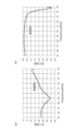
- Figure 4 shows S parameters of Example 1 and Comparative Example obtained by simulation.
- Figure 4(a) shows S11
- Figure 4(b) shows S21.
- S11 is the reflection characteristic at Port 1 shown in Figure 2(c)
- S21 is the transmission characteristic from Port 1 to Port 2 shown in Figure 2(c).
- the horizontal axis is frequency (Frequency [GHz])
- the vertical axis is S11 [dB].
- the horizontal axis is frequency (Frequency [GHz])
- the vertical axis is S21 [dB].
- Figures 4(a) and (b) show S11 and S12 by dashed lines in the case of using a transmission board in which the outer conductor 123 of the connector 120 and the ground conductor 113 of the dielectric board 111 are connected in a DC manner, as a comparative example.
- S11 of Example 1 is -20 dB or less in the frequency range of 27 GHz to 30 GHz. Moreover, S11 of Example 1 is smaller than S11 of the comparative example. And, as can be seen from S21 shown in FIG. 4(b), Example 1 has low loss in the frequency range of 27 GHz to 30 GHz, similar to the comparative example.
- the outer conductor 123 of the connector 120 is capacitively coupled to the ground conductor 113 of the transmission board 110 via the capacitive coupling conductor 114, and is not connected in a DC manner.
- the transmission characteristics (S11 and S21) of the transmission device 100 of Example 1 are small compared to (equal to) a transmission device in which the outer conductor 123 of the connector 120 is connected in a DC manner to the ground conductor 113 of the transmission board 110. That is, in the transmission device 100 of the first embodiment, the capacitive coupling conductor 114 is provided to capacitively couple the outer conductor 123 of the connector 120 and the ground conductor 113 of the transmission board 110, so there is no need to provide a through hole in the dielectric board 111 to directly connect the outer conductor 123 of the connector 120 and the ground conductor 113 of the transmission board 110. This reduces the manufacturing cost of the transmission device 100.
- the dimension (Rx+, Rx-, Ry+, Ry-) between the center O of the connector 120 and the outer edge of the capacitive coupling conductor 114 is more than 1/4 and less than 1/2 of the effective wavelength ⁇ g. This is because, if the dimension (Rx+, Rx-, Ry+, Ry-) between the center O of the connector 120 and the outer edge of the capacitive coupling conductor 114 is 1/4 or less of the effective wavelength ⁇ g, the amount of capacitive coupling between the outer conductor 123 of the connector 120 and the ground conductor 113 of the transmission board 110 is small, making it difficult for the outer conductor 123 of the connector 120 to be held at ground potential.
- the dimensions (Rx+, Rx-, Ry+, Ry-) from the center O of the connector 120 to the outer edge of the capacitive coupling conductor 114 may be set to be greater than 1/4 and less than 1/2 of the effective wavelength ⁇ g.
- the corresponding frequency corresponding to 1/4 ⁇ g is about 16 GHz, and the corresponding frequency corresponding to 1/2 ⁇ g is about 32 GHz.
- the corresponding frequency corresponding to 1/4 ⁇ g is about 20 GHz, and the corresponding frequency corresponding to 1/2 ⁇ g is about 39 GHz.
- the corresponding frequency corresponding to 1/4 ⁇ g is about 17 GHz
- the corresponding frequency corresponding to 1/2 ⁇ g is about 33 GHz.
- the transmission characteristics (S11, S21) are similar to (have a small difference from) those of a transmission device in which the outer conductor 123 of the connector 120 is DC-connected to the ground conductor 113 of the transmission board 110.
- the shape of the capacitive coupling conductor 114 can be set based on the effective wavelength ⁇ g, as in the first embodiment.
- n is an integer of 2 or more, except for the frequency where n ⁇ 1/2 ⁇ g, the difference becomes small (equal) to that of a transmission device in which the outer conductor 123 of the connector 120 is DC-connected to the ground conductor 113 of the transmission board 110.
- Example 1 is a case in which the thickness t of the dielectric substrate 111 is 0.127 mm
- Example 2 is a case in which the thickness t of the dielectric substrate 111 is 0.254 mm.
- Example 1 is Example 1 shown in FIGS. 3 and 4.
- Example 2 adjusts the dimensions of the parameters (Rx+, Rx-, Ry+, Ry-) of the capacitive coupling conductor 114 so as to achieve matching in the 28 GHz band.
- the dielectric substrate 111 is made larger than that in Example 1, and therefore the width W of the feeder line 112 is set to 0.6 mm in order to set the characteristic impedance to 50 ⁇ .
- FIG. 6 shows the S parameters of Example 1 and Example 2 obtained by simulation.
- FIG. 6(a) shows S11
- FIG. 6(b) shows S21.
- the horizontal and vertical axes in FIG. 6(a) and (b) are the same as those in FIG. 4(a) and (b).
- Example 1 shown in FIG. 6(a) and (b) is the same as that shown in FIG. 4(a) and (b).
- Example 2 in which the thickness t of the dielectric substrate 111 is doubled to 0.254 mm, S11 is smaller than in Example 1 in which the thickness t of the dielectric substrate 111 is 0.127 mm.
- the transmission characteristics are slightly lower than in Example 1, which indicates that the radiation loss has increased.
- the difference in the transmission characteristics (S11, S21) between Example 1 and Example 2 is small, and equivalent characteristics are obtained. In other words, even if the thickness t of the dielectric substrate 111 is changed, equivalent characteristics can be obtained by adjusting the shape of the capacitive coupling conductor 114.
- the capacitive coupling conductor 114 has a U-shaped planar shape and a shape surrounding the outer edge is a rectangle 115.
- the capacitive coupling conductor 114' has a U-shaped planar shape and a shape surrounding the outer edge is a circle 115'.
- FIG. 7 is a diagram for explaining a transmission device 100' to which the second embodiment is applied.
- FIG. 7(a) is a plan view
- FIG. 7(b) shows the parameters of Example 3 used in the simulation.
- the x-direction, y-direction, and z-direction shown in FIG. 7(a) are the same as those in FIG. 4(a).
- the capacitive coupling conductor 114' has a circular shape 115' with a radius R that surrounds the outer edge.
- the capacitive coupling conductor 114' has a circular opening ⁇ in the center, and a gap ⁇ that extends from the outer edge (circle 115') to the opening ⁇ .
- the rest of the configuration is the same as the transmission device 100 described in FIG. 4(a) and (b). Therefore, the same reference numerals are used and the description is omitted.
- the parameter of the capacitive coupling conductor 114' shown in FIG. 7(b) is the radius R of the circle 115', which is the dimension from the center of the connector 120 to the outer edge of the capacitive coupling conductor 114'.
- the relative dielectric constant ⁇ r of the dielectric substrate 111 is 2.19. Therefore, the effective wavelength ⁇ g is 7.24 mm.
- the thickness t of the dielectric substrate 111 is 0.127 mm, as in Example 1. Therefore, the width W of the feed line 112 is 0.37 mm, as in Example 1.
- the radius R is 2.9 mm, which is considered to have good characteristics at 28.5 GHz.
- the ratio (R/ ⁇ g) of the dimension (radius R) from the center O of the connector 120 to the edge of the capacitive coupling conductor 114' to the effective wavelength ⁇ g is 0.4, which is greater than 1/4 ⁇ g and less than 1/2 ⁇ g.
- Figure 8 shows the S parameters of Example 3 obtained by simulation.
- Figure 8(a) shows S11
- Figure 8(b) shows S21.
- the horizontal and vertical axes in Figures 8(a) and 8(b) are the same as those in Figures 4(a) and 4(b).
- the dielectric substrate 111 has a relative dielectric constant ⁇ r of 2.19.
- S11 in Example 3 is small in the vicinity of 29 GHz, similar to Example 1 shown in FIG. 4(a), but is large at frequencies lower than 29 GHz and higher than 29 GHz.
- the radius R is set to a value that is considered to have good characteristics at 28.5 GHz, as well as a mismatch that occurs between the transmission mode of the coaxial cable and the transmission mode of the transmission board 110 that constitutes the microstrip line.
- the shape surrounding the outer edge of the capacitive coupling conductor 114 is preferably the rectangle 115 of Example 1.
- S21 in Example 3 drops significantly near 34.7 GHz. This is because when the dimension from the center of the connector 120 to the outer edge of the capacitive coupling conductor 114' is 2.9 mm (radius R), the frequency corresponding to 1/2 ⁇ g is approximately 35 GHz. On the other hand, when the dimension from the center of the connector 120 to the outer edge of the capacitive coupling conductor 114' is 2.9 mm (radius R), the frequency corresponding to 1/4 ⁇ g is approximately 17 GHz. Therefore, the transmission device 100' operates in a frequency band above 17 GHz and below 35 GHz. As mentioned above, it operates in even higher frequency bands except for the vicinity of 35 GHz.
- the capacitive coupling conductor 114 has a U-shaped planar shape and a shape surrounding the outer edge is a rectangle 115.
- the capacitive coupling conductor 114'' has a U-shaped planar shape and a shape surrounding the outer edge is a pentagon (here, a regular pentagon) 115''.
- FIG. 9 is a diagram for explaining a transmission device 100'' to which the third embodiment is applied.
- FIG. 9(a) is a plan view
- FIG. 9(b) shows the parameters of Example 4 used in the simulation.
- the x-direction, y-direction, and z-direction shown in FIG. 9(a) are the same as those in FIG. 4(a).
- the shape surrounding the outer edge of the capacitive coupling conductor 114" is a pentagon 115".
- the dimension from the center of the connector 120 to the apex of the pentagon 115" is Rmax.
- the capacitive coupling conductor 114" has a circular opening ⁇ in the center, and a gap ⁇ that extends from the outer edge (pentagon 115") to the opening ⁇ .
- the gap ⁇ is provided on one side of the pentagon 115".
- the rest of the configuration is the same as that of the transmission device 100 described in FIGS. 4(a) and (b). Therefore, the same reference numerals are used and the description is omitted.
- the parameters of the capacitive coupling conductor 114" shown in FIG. 9(b) are the dimension from the center of the connector 120 to the outer edge of the capacitive coupling conductor 114', which is the dimension from the center to the apex of the pentagon 115".
- the relative dielectric constant ⁇ r of the dielectric substrate 111 is 2.19. Therefore, the effective wavelength ⁇ g is 7.24 mm.
- the thickness t of the dielectric substrate 111 is 0.127 mm, as in Example 1. Therefore, the width W of the feed line 112 is 0.37 mm, as in Example 1.
- Rmax is 3.2 mm, which is considered to have good characteristics at 28.5 GHz.
- the ratio (Rmax/ ⁇ g) of the maximum dimension (Rmax) from the center O of the connector 120 (the center of the pentagon 115") to the edge of the capacitive coupling conductor 114" to the effective wavelength ⁇ g is 0.44, which is greater than 1/4 ⁇ g and less than 1/2 ⁇ g.
- Figure 10 shows the S parameters of Example 4 obtained by simulation.
- Figure 10(a) shows S11
- Figure 10(b) shows S21.
- the horizontal and vertical axes in Figures 10(a) and 10(b) are the same as those in Figures 4(a) and 4(b).
- the dielectric substrate 111 has a relative dielectric constant ⁇ r of 2.19.
- S11 in Example 4 is small in the vicinity of 29 GHz, similar to Example 1 shown in FIG. 4(a), but becomes large at frequencies lower than 29 GHz and higher than 29 GHz. Note that S11 becomes small again in the vicinity of 34.4 GHz.
- Example 4 S21 drops significantly near 33.5 GHz.
- Rmax 3.2 mm
- the frequency corresponding to 1/2 ⁇ g is approximately 32 GHz.
- Rmin 2.6 mm
- the frequency corresponding to 1/2 ⁇ g is approximately 39 GHz.
- 33.5 GHz the frequency at which S21 drops, is between these frequencies.
- the frequency at which S21 drops is determined between the maximum dimension (Rmax) and minimum dimension (Rmin) from the center of the connector 120 to the outer edge of the capacitive coupling conductor 114". Therefore, in order to suppress the decrease in S21 in the frequency band, it is preferable to use as the upper limit the frequency at which the maximum dimension (Rmax) from the center of the connector 120 to the outer edge of the capacitive coupling conductor 114" corresponds to 1/2 ⁇ g.
- the lower limit the frequency at which the minimum dimension (Rmin) from the center of the connector 120 to the outer edge of the capacitive coupling conductor 114" corresponds to 1/4 ⁇ g.
- the shape of the capacitive coupling conductor can be set based on the desired frequency band. It is preferable to use as the upper limit the frequency at which the maximum dimension from the center of the connector 120 to the outer edge of the capacitive coupling conductor 114" corresponds to 1/4 ⁇ g.
- n is an integer equal to or greater than 2
- the transmission device operates in a wider frequency band, except for the frequency where n ⁇ 1/4 ⁇ g. Therefore, the shape of the capacitive coupling conductor 114" can be set to match the frequency band.
- the capacitive coupling conductors 114, 114', and 114" have been described.
- the capacitive coupling conductors 114, 114', and 114" form a capacitance (capacitor) between themselves and the ground conductor 113. Therefore, the area of the capacitive coupling conductors 114, 114', and 114" depends on the coupling capacitance between the outer conductor 123 of the connector 120 and the ground conductor 113 of the transmission board 110.
- the dimension from the center of the connector 120 to the edge of the capacitive coupling conductors 114, 114', and 114" affects the frequency of the signal.
- the shape of the capacitive coupling conductors 114, 114', and 114" can be set according to the coupling capacitance between the outer conductor 123 of the connector 120 and the ground conductor 113 of the transmission board 110 and the frequency of the signal to be transmitted. In this way, there is no need to provide a through hole or the like in the dielectric board 111, and therefore the manufacturing costs of the transmission devices 100, 100', and 100" can be reduced.
- the shapes surrounding the outer edges of the capacitive coupling conductors 114, 114', 114" described in the first, second, and third embodiments were square, circular, and pentagonal (regular pentagon).
- the shapes surrounding the outer edges of the capacitive coupling conductors may be polygonal (including square and pentagon), circular, elliptical, and other shapes. Also, like the capacitive coupling conductor 114 shown in the first embodiment, a part may be removed, or other shapes may be added.
- the pitch of the radiating element 300 in the left-right direction ( ⁇ x direction) is determined by the wavelength of the radio waves transmitted and received by the radiating element 300.
- the shape surrounding the edge of the capacitive coupling conductor is a shape that is narrow in the left-right direction ( ⁇ x direction), such as a square or ellipse. In this way, the shape of the capacitive coupling conductor 114 can be adapted to the application.
Landscapes
- Waveguide Aerials (AREA)
- Waveguides (AREA)
Abstract
Description
本発明は、伝送装置及びアンテナに関する。 The present invention relates to a transmission device and an antenna.
特許文献1には、基板の一方の面に配設された所定の幅を有する中心導体と、基板の他方の面に配設された接地導体とを備えたマイクロストリップ線路の接続構造において、前記基板の中心導体が配設された導体配設面に前記接地導体と接続するアースパターンを形成し、コネクタ内部導体とコネクタ外導体とを備えたコネクタを前記導体配設面に取り付け、コネクタ内部導体を前記マイクロストリップ線路の中心導体に接続するとともに、コネクタ外導体を前記アースパターンに接続するマイクロストリップ線路の接続構造が記載されている。
ところで、マイクロストリップアンテナなどでは、誘電体基板の一方の面に電波を送受信する放射素子が接続された給電線路が設けられ、他方の面に接地導体が設けられた伝送基板(いわゆるプリント基板)と、同軸ケーブルが接続されて信号の入出力端子となるコネクタとを備えた伝送装置が用いられる。SMPM(Sub Miniature Push-on Mini)などの外寸の小さいコネクタは、伝送基板の給電線路が設けられた側に実装される。このため、誘電体基板に内側が導体で覆われたスルーホールなどを介して、コネクタの外導体と伝送基板の接地導体とを接続することが行われてきた。しかし、スルーホールなどを設けると、伝送装置の製造費が高くなる。このため、コネクタの外導体と伝送基板の接地導体とを接続するスルーホールなどを設けないことが求められている。
本発明は、伝送基板の接地導体とコネクタの外導体とを接続しなくとも動作する伝送装置などを提供する。
In the case of a microstrip antenna, a transmission device is used that includes a transmission board (so-called printed circuit board) having a feeder line connected to a radiating element that transmits and receives radio waves on one side of a dielectric board and a ground conductor on the other side, and a connector that serves as an input/output terminal for signals to which a coaxial cable is connected. Connectors with small external dimensions, such as SMPM (Sub Miniature Push-on Mini), are mounted on the side of the transmission board where the feeder line is provided. For this reason, the outer conductor of the connector and the ground conductor of the transmission board have been connected via a through hole or the like whose inside is covered with a conductor in the dielectric board. However, providing a through hole or the like increases the manufacturing cost of the transmission device. For this reason, it is required not to provide a through hole or the like that connects the outer conductor of the connector and the ground conductor of the transmission board.
The present invention provides a transmission device that operates without connecting the ground conductor of the transmission board and the outer conductor of the connector.
請求項1に記載の発明は、板状の誘電体基板の一方の面に設けられた給電線路、及び容量結合導体と、当該誘電体基板の他方の面に設けられた接地導体とを備え、信号を伝送する伝送基板と、内導体と当該内導体の外側に設けられた外導体とを備え、信号を入出力するコネクタと、を備え、前記コネクタは、前記伝送基板の前記給電線路及び前記容量結合導体が設けられた前記一方の面に設けられ、当該コネクタの前記内導体が当該給電線路に接続され、前記外導体が当該容量結合導体と接続され、当該伝送基板の前記接地導体と当該コネクタの当該外導体とが接続されていない伝送装置である。
請求項2に記載の発明は、前記伝送基板において、前記容量結合導体と前記接地導体とは、前記誘電体基板を介して対向していることを特徴とする請求項1に記載の伝送装置である。
請求項3に記載の発明は、前記伝送基板の前記接地導体と、前記コネクタの前記外導体とは、容量結合していることを特徴とする請求項2に記載の伝送装置である。
請求項4に記載の発明は、前記容量結合導体は、中央部に開口と、外縁から当該開口までに至る間隙とを有し、当該間隙に前記給電線路の端部が位置することを特徴とする請求項1乃至3のいずれか1項に記載の伝送装置である。
請求項5に記載の発明は、前記容量結合導体の外縁を囲む形状が、多角形、円形、楕円形のいずれかであることを特徴とする請求項1乃至4のいずれか1項に記載の伝送装置である。
請求項6に記載の発明は、前記コネクタの中心から前記容量結合導体の外縁までの寸法が前記誘電体基板における実効波長の1/4超、且つ1/2未満であることを特徴とする請求項1乃至5のいずれか1項に記載の伝送装置である。
請求項7に記載の発明は、前記コネクタの中心から前記容量結合導体の外縁までの寸法の内、最小の寸法が実効波長の1/4に対応する周波数を下限とし、最大の寸法が実効波長の1/2に対応する周波数を上限とした信号を伝送することを特徴とする請求項1乃至5のいずれか1項に記載の伝送装置である。
請求項8に記載の発明は、電波を送受信する放射素子と、前記放射素子が接続され、当該放射素子が送受信した電波に基づく信号を伝送する、請求項1乃至7のいずれか1項に記載の伝送装置と、を備えるアンテナである。
請求項9に記載の発明は、前記コネクタの中心から前記容量結合導体の外縁までの寸法の内、最小の寸法が実効波長の1/4に対応する周波数を下限とし、最大の寸法が実効波長の1/2に対応する周波数を上限とした電波を送受信することを特徴とする請求項8に記載のアンテナである。
The invention described in
A second aspect of the present invention provides a transmission device according to the first aspect, wherein in the transmission board, the capacitive coupling conductor and the ground conductor face each other via the dielectric substrate.
A third aspect of the present invention provides the transmission device according to the second aspect, wherein the ground conductor of the transmission board and the outer conductor of the connector are capacitively coupled.
The invention described in claim 4 is a transmission device described in any one of
The invention recited in
The invention described in claim 6 is a transmission device described in any one of
The invention described in claim 7 is a transmission device described in any one of
The invention described in claim 8 is an antenna comprising a radiating element that transmits and receives radio waves, and a transmission device described in any one of
The invention described in claim 9 is the antenna described in claim 8, characterized in that it transmits and receives radio waves with a frequency corresponding to 1/4 of the effective wavelength as the lower limit of the dimension from the center of the connector to the outer edge of the capacitive coupling conductor, and a frequency corresponding to 1/2 the effective wavelength as the upper limit of the dimension from the center of the connector to the outer edge of the capacitive coupling conductor.
請求項1、8に記載の発明によれば、伝送基板の接地導体とコネクタの外導体とを接続しなくとも動作する。
請求項2に記載の発明によれば、対向していない場合に比べ、結合容量を大きくできる。
請求項3に記載の発明によれば、直流的な接続を要しない。
請求項4に記載の発明によれば、一層の導電体層で構成できる。
請求項5に記載の発明によれば、用途に合わせた形状にできる。
請求項6に記載の発明によれば、容量結合導体の形状が実効波長に基づいて設定できる。
請求項7、9に記載の発明によれば、容量結合導体の形状が周波数帯域に基づいて設定できる。
According to the first and eighth aspects of the present invention, operation is possible without connecting the ground conductor of the transmission board and the outer conductor of the connector.
According to the second aspect of the present invention, the coupling capacitance can be made larger than in a case where the electrodes are not opposed to each other.
According to the third aspect of the present invention, no DC connection is required.
According to the fourth aspect of the present invention, the conductive layer can be formed of a single conductive layer.
According to the fifth aspect of the present invention, the shape can be adjusted to suit the application.
According to the sixth aspect of the present invention, the shape of the capacitive coupling conductor can be set based on the effective wavelength.
According to the seventh and ninth aspects of the present invention, the shape of the capacitive coupling conductor can be set based on the frequency band.
以下、添付図面を参照して、本発明の実施の形態について詳細に説明する。なお、本実施の形態では、マイクロストリップアンテナを例に、伝送装置を説明するが、伝送装置は、信号を伝送する装置であって、信号の入出力にコネクタを介して同軸ケーブルが接続されるものである。伝送装置は、アンテナ素子を含まない。よって、伝送装置は、アンテナ素子が接続されてマイクロストリップアンテナとして用いられてもよく、信号から特定の周波数の信号を取り出すフィルタ素子が接続されてフィルタとして用いられてもよい。さらに、他の機能を有する素子が接続されてもよい。 Below, an embodiment of the present invention will be described in detail with reference to the attached drawings. In this embodiment, a transmission device will be described using a microstrip antenna as an example. The transmission device is a device that transmits signals, and a coaxial cable is connected to the signal input and output via a connector. The transmission device does not include an antenna element. Therefore, the transmission device may be connected to an antenna element and used as a microstrip antenna, or connected to a filter element that extracts a signal of a specific frequency from a signal and used as a filter. Furthermore, elements having other functions may be connected.
図1は、ミリ波帯のマイクロストリップアンテナを説明する図である。図1(a)は、外寸の小さいコネクタ120を用いたマイクロストリップアンテナ1、図1(b)は、外寸の大きいコネクタ220を用いたマイクロストリップアンテナ2である。図1(a)において、紙面の上側にマイクロストリップアンテナ1を、紙面の下側にコネクタ120の斜視図を示す。同様に、図1(b)において、紙面の上側にマイクロストリップアンテナ2を、紙面の下側にコネクタ220の斜視図を示す。図1(a)のマイクロストリップアンテナ1において、紙面の右方向をx方向、紙面の上方向をy方向、紙面の表面方向をz方向とする。図1(b)のマイクロストリップアンテナ2においても同様とする。ここでは、マイクロストリップアンテナ1及びマイクロストリップアンテナ2は、ミリ波帯の電波を送受信するとする。
FIG. 1 is a diagram explaining a microstrip antenna in the millimeter wave band. FIG. 1(a) shows a
図1(a)に示すマイクロストリップアンテナ1は、伝送装置100と、放射素子300とを備える。伝送装置100は、伝送基板110とコネクタ120とを備える。伝送基板110は、板状の誘電体基板111と、誘電体基板111の一方の面(以下では、表面と表記する。)に設けられた給電線路112と、誘電体基板111の他方の面(以下では、裏面と表記する。)に設けられた接地導体113(符号のみを表記する)と、を備える。なお、伝送基板110は、表面に容量結合導体114(後述する図2(a)など参照)を備えるが、図1(a)では、省略する。そして、放射素子300は、誘電体基板111の給電線路112に接続されるように設けられている。なお、マイクロストリップアンテナ1の放射素子300は、電波を送受信するが、ここでは、放射素子300と表記する。
The
誘電体基板111は、例えば、ガラス布基材にエポキシ樹脂、ポリイミド樹脂、フッ素樹脂などを含浸させて構成されている。給電線路112、接地導体113は、銅(Cu)箔などの導電体で構成されている。ここでは、導体とは、電気の良導体である導電体を意味する。給電線路112は、誘電体基板111の表面に予め定められた幅の帯状に設けられている。給電線路112の幅は、伝送される信号に対する特性インピーダンスによって設定される。接地導体113は、誘電体基板111の裏面の全面を覆うように設けられている。なお、接地導体113は、必ずしも誘電体基板111の裏面の全面を覆わなくてもよく、給電線路112に対向するように設けられていればよい。ここでは、伝送基板110は、両面に銅(Cu)箔などの導電体が設けられ、銅箔が給電線路112、接地導体113などに加工された誘電体基板111である。つまり、伝送基板110は、誘電体基板111に加え、給電線路112や接地導体113などを含む。伝送基板110は、プリント基板と表記されることがある。また、誘電体基板111の表面に給電線路112、裏面に接地導体113を設けた構成は、マイクロストリップ線路と表記されることがある。
The
図1(a)に示す放射素子300は、いわゆるパッチアンテナであって、放射部と地板とを備える。放射部は、誘電体基板111の表面の導電体により構成される。図1(a)では、放射部の平面形状は、一例として正方形である。そして、誘電体基板111の裏面に設けられ接地導体113が地板として機能する。接地導体113は、放射部と対向するように設けられている。なお、放射部は、給電線路112と同じ導電体を加工して構成されている。以下では、放射部を放射素子300とし、地板については説明を省略する。なお、放射素子300は、パッチアンテナでなくともよく、給電線路112に接続されて給電されるものであればよい。
The radiating
図1(a)に示すマイクロストリップアンテナ1は、誘電体基板111の表面に紙面の右方向(x方向)に3個、紙面の上方向(y方向)に3個が配列された9個の放射素子300を備える。給電線路112は、紙面の上方向(y方向)に3個の放射素子300を順に接続する。図1(a)に示すマイクロストリップアンテナ1では、3個の給電線路112を備える。そして、それぞれの給電線路112の一端部(紙面の下方であって-y方向の端部)がコネクタ120に接続されている。ここで、コネクタ120は、外寸が小さい、例えばSMPMである。コネクタ120の外寸が小さければ、コネクタ120は、紙面の左右方向(±x方向)における放射素子300の配列のピッチで配列される。
The
マイクロストリップアンテナ1のように、複数の放射素子を備えるアンテナは、送信側の複数の放射素子から同時に信号を送信し、その信号を受信側の複数の放射素子で受信して通信を高速化するMIMO(Multiple Input Multiple Output)方式の無線通信や、放射する電波の形状の整形(ビームフォーミングなど)などに使用される。
Antennas equipped with multiple radiating elements, such as the
図1(b)に示すマイクロストリップアンテナ2は、伝送装置200と、放射素子300とを備える。伝送装置200は、伝送基板210とコネクタ220とを備える。伝送基板210は、誘電体基板211と、誘電体基板211の表面に設けられた給電線路212と、誘電体基板211の裏面に設けられた接地導体213(符号のみを表記する)と、を備える。そして、放射素子300は、誘電体基板211の給電線路212に接続されるように設けられている。
The
マイクロストリップアンテナ2は、誘電体基板211の表面に配列された9個の放射素子300を備える。そして、マイクロストリップアンテナ2は、紙面の上方向において3個の放射素子300を接続する3個の給電線路212を備える。そして、3個の給電線路212は、一端部(紙面の下方であって-y方向の端部)がコネクタ220に接続されている。マイクロストリップアンテナ1及びマイクロストリップアンテナ2は、同じミリ波帯の電波を送受信することから、9個の放射素子300の形状及び配列は、マイクロストリップアンテナ1と同様である。ここで、コネクタ220は、例えば、外寸が上記のSMPMに比べ大きいSMA(Sub Miniature Type A)である。コネクタ220の外寸が大きい場合、図1(b)に示すように、コネクタ220は、紙面の左右方向(±x方向)における放射素子300の配列のピッチで配列されない。このため、コネクタ220は、紙面の横方向(x方向)において、放射素子300の配列のピッチより大きいピッチで配列される。よって、給電線路212は、ピッチの違いを吸収するため、折り曲げられて構成される。
The
上述したことから、外寸が大きいコネクタ220を用いたマイクロストリップアンテナ2の誘電体基板211は、外寸が小さいコネクタ120を用いたマイクロストリップアンテナ1の誘電体基板111に比べ大きくなる。また、外寸が大きいコネクタ220を用いたマイクロストリップアンテナ2の給電線路212は、外寸が小さいコネクタ120を用いたマイクロストリップアンテナ1の給電線路112に比べ長くなって損失が大きくなる。したがって、ミリ波帯のような波長が短い電波を送受信するアンテナでは、外寸が小さいコネクタを用いることがよい。
As described above, the
次に、コネクタ120、220について説明する。
SMAなどの外寸が大きいコネクタ220は、図1(b)の下側に示す斜視図から分かるように、誘電体基板211に貫通孔を設け、誘電体基板211の接地導体213が設けられる裏面から挿入して実装される。つまり、コネクタ220の外導体が接地導体213に接触し、コネクタ220の内導体(心線)は、貫通孔を通って給電線路212に接続される。
Next, the
1(b), a
一方、SMPMなどの外寸が小さいコネクタ120は、図1(a)の下側に示す斜視図から分かるように、誘電体基板111の表面、つまり給電線路112が設けられる表面に実装される。すなわち、コネクタ120の外導体と誘電体基板111に設けられた接地導体113とが、伝送基板110の異なる面に配置される。このため、コネクタ120の外導体と、伝送基板110の接地導体113とは、誘電体基板111に内側に導体が設けられた(例えば、金属メッキされた)スルーホールなどを介して接続されていた。しかし、このようなスルーホールを形成すると、マイクロストリップアンテナ1の製造費が高くなる。
On the other hand, a
そこで、本実施の形態が適用される伝送装置100は、伝送基板110の接地導体113とコネクタ120の外導体123(後述する図2(b)参照)とを接続しなくとも(非接触であっても)動作するようになっている。つまり、本実施の形態が適用される伝送装置100では、スルーホールを設けることを要しない。
The
[第1の実施の形態]
図2は、第1の実施の形態が適用される伝送装置100を説明する図である。図2(a)は、伝送基板110とコネクタ120とを近接させた状態の斜視図、図2(b)は、コネクタ120の斜視図、図2(c)は、伝送基板110にコネクタ120を実装した状態の斜視図である。図2(a)、(b)、(c)において、図示のようにx方向、y方向、及びz方向を設定する。
[First embodiment]
Fig. 2 is a diagram for explaining a
図2(a)に示すように、伝送基板110は、誘電体基板111と、給電線路112と、接地導体113と、容量結合導体114とを備える。給電線路112及容量結合導体114は、誘電体基板111の表面(+x方向の面)に設けられている。給電線路112及び容量結合導体114は、誘電体基板111の表面に設けられた導体(銅箔など)で構成されている。給電線路112と容量結合導体114とは、接続されていない。
As shown in FIG. 2(a), the
給電線路112の平面形状(+z方向から見た形状)は、前述したように帯状である。給電線路112は、誘電体基板111の比誘電率などで幅Wが決められ、信号の伝送に対する特性インピーダンスに設定される。特性インピーダンスは、例えば50Ωである。
The planar shape of the power supply line 112 (shape when viewed from the +z direction) is strip-shaped as described above. The width W of the
容量結合導体114は、平面形状がU字状の導体である。容量結合導体114は、外縁を囲む形状が四角形115(図3(b)参照。ここでは、長方形)であるが、中央部に円形の開口α、上方(+y方向)に外縁から開口αに至る空隙βを有している。つまり、容量結合導体114は、外縁を囲む形状が四角形で、上方に開いたU字状である。そして、給電線路112の下方の端部(-y方向の端部)が容量結合導体114の空隙βに位置する。さらに、容量結合導体114は、右下部(-y方向且つ+x方向の端部)と、左下部(-y方向且つ-x方向の端部)とにおいて、四角形115から一部が除去されている。このように、容量結合導体114の外縁を囲む形状は、四角形や、後述する円、五角形などでに限定されるものでなく、これらの形状から一部が除去された形状、他の形状を付加した形状であってもよい。そして、容量結合導体114の外縁を囲む形状とは、間隙が設けられていないとして容量結合導体114の外側の縁に沿って囲んだ(繋いだ)形状であって、さらに除去された一部を含むように囲む形状である。容量結合導体114の平面形状をU字状にすることにより、給電線路112と容量結合導体114とが1層の導電体で構成される。
The
接地導体113は、符号のみを表記するが、誘電体基板111の裏面の全面に設けられている。よって、給電線路112及び容量結合導体114と接地導体113とは、誘電体基板111を挟んで対向している。
The
コネクタ120はSMPMであって、図2(b)に示すように、絶縁体121と、内導体122と、外導体123とを備える。内導体122は、信号が通る導体であって、心線と表記されることがある。内導体122は、L字状に曲げられている。つまり、内導体122は、誘電体基板111に垂直である部分と、誘電体基板111に平行である部分とを備える。そして、内導体122は、誘電体基板111に平行である部分の先端部が、伝送基板110の給電線路112に接続される。
The
外導体123は、伝送基板110に実装される実装部123aと、同軸ケーブルに接続される接続される接続部123bとを備える。実装部123aは、伝送基板110側の面(-z方向の面)である底面123a1が平坦になっている。そして、コネクタ120の実装部123aの底面123a1が、伝送基板110の容量結合導体114に接続される。接続部123bは、同軸ケーブル側のコネクタとプッシュオンロック機構で接続が容易になっていてもよい。
The
内導体122と外導体123との間に、絶縁体121が設けられている。絶縁体121は、内導体122と外導体123との間において直流に対する絶縁を行う。なお、内導体122及び外導体123は、銅又は銅合金で構成されている。絶縁体121は、高周波の信号に対する損失が小さい、ポリテトラフルオロエチレンなどの樹脂で構成されている。なお、図2(b)に示したコネクタ120(絶縁体121、内導体122、及び外導体123)の形状は、一例であって、他の形状であってもよい。
The
図2(c)に示すように、コネクタ120は、誘電体基板111に実装される。内導体122と給電線路112との接続、及び外導体123と容量結合導体114との接続は、はんだなどで行えばよい。コネクタ120の内導体122をPort1とし、給電線路112の上方の端部(+y方向の端部)をPort2とする。
As shown in FIG. 2(c), the
図3は、第1の実施の形態が適用される伝送装置100を説明する図である。図3(a)は、平面図、図3(b)は、側面図、図3(c)は、シミュレーションに用いた実施例1のパラメータを示す。図3(a)において、紙面の右方向をx方向、紙面の上方向をy方向、紙面の表面方向をz方向とする。図3(b)では、紙面の右方向がz方向、紙面の上方向がy方向、紙面の裏面方向がz方向である。なお、コネクタ120は、オス型である。
FIG. 3 is a diagram illustrating a
図3(a)の平面図は、伝送基板110上に実装されたコネクタ120側から見た図である。コネクタ120は、伝送基板110上の給電線路112及び容量結合導体114に重なって設けられている。図3(a)では、給電線路112及び容量結合導体114を太線、コネクタ120を細線で示している。そして、コネクタ120で隠れた容量結合導体114を破線で示している。ここでは、コネクタ120の内導体122において、誘電体基板111に垂直な部分の中心、つまり同軸ケーブルが接続される側の内導体122の中心をコネクタ120の中心Oとする。そして、コネクタ120の中心Oから、容量結合導体114の+x方向の端部までをRx+、容量結合導体114の-x方向の端部までをRx-、容量結合導体114の+y方向の端部までをRy+、容量結合導体114の-y方向の端部までをRy-とする。
The plan view of Figure 3(a) is a view seen from the
図3(b)の側面図は、図3(a)に示した伝送装置100を-x方向側から見た図である。伝送基板110は、前述したように、誘電体基板111と、誘電体基板111の表面(+z方向側の面)に設けられた給電線路112、容量結合導体114と、誘電体基板111の裏面(-z方向側の面)に設けられた接地導体113とを備える。そして、容量結合導体114にコネクタ120の外導体123における実装部123aが接続され、給電線路112にコネクタ120の内導体122が接続されている。なお、図3(b)では、コネクタ120の外導体123で隠れた内導体122の部分を破線で示している。
The side view of FIG. 3(b) is a view of the
図3(b)から分かるように、コネクタ120の外導体123と、伝送基板110の接地導体113とは、誘電体基板111を介して対向している。そして、コネクタ120の外導体123と、伝送基板110の接地導体113とは、直流的に接続されていない。つまり、コネクタ120の外導体123と、伝送基板110の接地導体113とを、容量結合導体114を介して容量結合させている。容量結合導体114と接地導体113とを対向させることにより、結合容量を大きくできる。
As can be seen from FIG. 3(b), the
給電線路112は、コネクタ120の内導体122と接続が容易になるように先端部(コネクタ120の内導体122と接続される部分)の形状が定められている。容量結合導体114の面積は、コネクタ120の外導体123における実装部123aの底面123a1の形状ばかりでなく、信号の波長、容量結合量などに応じて設定される。
The shape of the tip (the portion connected to the
図3(c)は、28GHz帯で整合させた場合における容量結合導体114のパラメータの寸法を示している。なお、誘電体基板111の比誘電率εrを2.19、誘電体基板111の厚さtを0.127mmとした。28GHzは、自由空間での周波数である。誘電体基板111内の実効波長λgは、自由空間での波長λと誘電体基板111の比誘電率εrとから、λ/sqrt(εr)で求められる。28GHzの場合、実効波長λgは、7.24mmとなる。ここでは、給電線路112は、特性インピーダンスを50Ωとし、幅Wを0.37mmとした。そして、図3(c)に示すように、容量結合導体114のパラメータ(Rx+、Rx-、Ry+、Ry-)の寸法を設定すると、容量結合導体114のパラメータ(Rx+、Rx-、Ry+、Ry-)の寸法と実効波長λgとの比の値(寸法/λg)は、1/4λg(0.25λg)を超え、1/2λg(0.5λg)未満となるように設定されている。上記の伝送装置100を実施例1とする。なお、図3(c)では、図3(a)に示したように、伝送装置100が左右方向(±x方向)で対称であることから、Rx+とRx-とを同じ値にしたが、同じでなくてもよい。
Figure 3 (c) shows the dimensions of the parameters of the
図4は、シミュレーションによって求めた実施例1と比較例のSパラメータである。図4(a)は、S11、図4(b)は、S21である。S11は、図2(c)に示したPort1における反射特性、S21は、図2(c)に示したPort1からPort2への透過特性である。図4(a)において、横軸は周波数(Frequency [GHz])、縦軸はS11[dB]である。図4(b)において、横軸は周波数(Frequency [GHz])、縦軸はS21[dB]である。なお、図4(a)、(b)には、比較例として、コネクタ120の外導体123と誘電体基板111の接地導体113とを直流的に接続した伝送基板を用いた場合におけるS11、S12を破線で示す。
Figure 4 shows S parameters of Example 1 and Comparative Example obtained by simulation. Figure 4(a) shows S11, and Figure 4(b) shows S21. S11 is the reflection characteristic at
図4(a)に示すように、実施例1のS11は、27GHz~30GHzの周波数範囲において-20dB以下である。しかも、実施例1のS11は、比較例のS11より小さい。そして、図4(b)に示すS21から分かるように、実施例1は、27GHz~30GHzの周波数範囲において、比較例と同様に損失が少ない。実施例1の伝送装置100では、コネクタ120の外導体123は、伝送基板110の接地導体113と容量結合導体114を介して容量結合し、直流的に接続されていない。しかし、実施例1の伝送装置100の伝送特性(S11及びS21)は、コネクタ120の外導体123を伝送基板110の接地導体113と直流的に接続した伝送装置と差が小さい(同等である)。すなわち、実施例1の伝送装置100では、容量結合導体114を設けてコネクタ120の外導体123と伝送基板110の接地導体113とを容量結合させることで、誘電体基板111にスルーホールを設けてコネクタ120の外導体123と伝送基板110の接地導体113とを直流的に接続することを要しない。よって、伝送装置100の製造費が抑制される。
As shown in FIG. 4(a), S11 of Example 1 is -20 dB or less in the frequency range of 27 GHz to 30 GHz. Moreover, S11 of Example 1 is smaller than S11 of the comparative example. And, as can be seen from S21 shown in FIG. 4(b), Example 1 has low loss in the frequency range of 27 GHz to 30 GHz, similar to the comparative example. In the
以上において、コネクタ120の中心Oと容量結合導体114の外縁までの寸法(Rx+、Rx-、Ry+、Ry-)は、実効波長λgの1/4超、且つ1/2未満であると説明した。これは、コネクタ120の中心Oと容量結合導体114の外縁までの寸法(Rx+、Rx-、Ry+、Ry-)が実効波長λgの1/4以下であると、コネクタ120の外導体123と伝送基板110の接地導体113との容量結合量が小さくて、コネクタ120の外導体123が接地電位に保持されにくくなる。一方、コネクタ120の中心Oと容量結合導体114の外縁までの寸法(Rx+、Rx-、Ry+、Ry-)が実効波長λgの1/2となると、励振が生じて電波を放射する(アンテナになる)。よって、コネクタ120の中心Oと容量結合導体114の外縁までの寸法(Rx+、Rx-、Ry+、Ry-)は、実効波長λgの1/4超、且つ1/2未満に設定されるとよい。コネクタ120の中心Oと容量結合導体114の外縁までの寸法が2.3mmの場合(Rx+、Rx-の場合)、1/4λgに対応する対応する周波数は約16GHz、1/2λgに対応する周波数は約32GHzである。コネクタ120の中心Oと容量結合導体114の外縁までの寸法が2.6mmの場合(Ry+の場合)、1/4λgに対応する対応する周波数は約20GHz、1/2λgに対応する周波数は約39GHzである。コネクタ120の中心Oと容量結合導体114の外縁までの寸法が3.0mmの場合(Ry-の場合)、1/4λgに対応する対応する周波数は約17GHz、1/2λgに対応する周波数は約33GHzである。よって、図4(a)、(b)の実施例1に示すように、27GHzから30GHzの周波数範囲において、伝送特性(S11、S21)は、コネクタ120の外導体123を伝送基板110の接地導体113と直流的に接続した伝送装置と差が小さい(同等である)ことになる。このようにすれば、実施例1のように、実効波長λgに基づいて容量結合導体114の形状が設定できる。
なお、後述するが、nを2以上の整数とした場合、n×1/2λgとなる周波数を除けば、コネクタ120の外導体123を伝送基板110の接地導体113と直流的に接続した伝送装置と差が小さく(同等に)なる。
In the above, it has been explained that the dimension (Rx+, Rx-, Ry+, Ry-) between the center O of the
As will be described later, when n is an integer of 2 or more, except for the frequency where n×1/2λg, the difference becomes small (equal) to that of a transmission device in which the
次に、誘電体基板111の厚さtについて説明する。
図5は、誘電体基板111の厚さtを異ならせた実施例1、2のパラメータを示す。実施例1は、誘電体基板111の厚さtが0.127mmの場合、実施例2は、誘電体基板111の厚さtが0.254mmの場合である。実施例1は、図3、図4に示した実施例1である。実施例2は、28GHz帯で整合するように容量結合導体114のパラメータ(Rx+、Rx-、Ry+、Ry-)の寸法を調整した。実施例2では、実施例1に比べて誘電体基板111を大きくしたことから、特性インピーダンスを50Ωに設定するため給電線路112の幅Wを0.6mmとしている。
Next, the thickness t of the
5 shows the parameters of Examples 1 and 2 in which the thickness t of the
図6は、シミュレーションによって求めた実施例1、実施例2のSパラメータである。図6(a)は、S11、図6(b)は、S21である。図6(a)、(b)における横軸及び縦軸は、図4(a)、(b)と同様である。なお、図6(a)、(b)に示す実施例1は、図4(a)、(b)に示したものと同じである。 FIG. 6 shows the S parameters of Example 1 and Example 2 obtained by simulation. FIG. 6(a) shows S11, and FIG. 6(b) shows S21. The horizontal and vertical axes in FIG. 6(a) and (b) are the same as those in FIG. 4(a) and (b). Note that Example 1 shown in FIG. 6(a) and (b) is the same as that shown in FIG. 4(a) and (b).
図6(a)に示すように、誘電体基板111の厚さtを0.254mmと2倍にした実施例2では、誘電体基板111の厚さtが0.127mmの実施例1に比べ、S11が小さくなる。一方、図6(b)に示すように、実施例2では、実施例1に比べ、通過特性が若干低下していることから、放射損失が増加していることが分かる。しかし、実施例1と実施例2とで、伝送特性(S11、S21)の差が小さく、同等の特性が得られる。すなわち、誘電体基板111の厚さtを変更しても、容量結合導体114の形状を調整することにより、同等の特性が得られる。
As shown in Figure 6 (a), in Example 2 in which the thickness t of the
[第2の実施の形態]
第1の実施の形態が適用される伝送装置100では、容量結合導体114は、平面形状がU字状であって、外縁を囲む形状が四角形115であった。第2の実施の形態が適用される伝送装置100′では、容量結合導体114′の平面形状はU字状であるが、外縁を囲む形状を円形115′とした。
[Second embodiment]
In the
図7は、第2の実施の形態が適用される伝送装置100′を説明する図である。図7(a)は、平面図、図7(b)は、シミュレーションに用いた実施例3のパラメータを示す。図7(a)に示す、x方向、y方向、及びz方向は、図4(a)と同様である。 FIG. 7 is a diagram for explaining a transmission device 100' to which the second embodiment is applied. FIG. 7(a) is a plan view, and FIG. 7(b) shows the parameters of Example 3 used in the simulation. The x-direction, y-direction, and z-direction shown in FIG. 7(a) are the same as those in FIG. 4(a).
図7(a)に示すように、容量結合導体114′は、外縁を囲む形状が半径Rの円形115′である。容量結合導体114′は、中央部に円形の開口αを備え、外縁(円形115′)から開口αに至る空隙βを備える。他の構成は、図4(a)、(b)で説明した伝送装置100と同様である。よって、同じ符号を付して説明を省略する。
As shown in FIG. 7(a), the capacitive coupling conductor 114' has a circular shape 115' with a radius R that surrounds the outer edge. The capacitive coupling conductor 114' has a circular opening α in the center, and a gap β that extends from the outer edge (circle 115') to the opening α. The rest of the configuration is the same as the
図7(b)に示す容量結合導体114′のパラメータは、コネクタ120の中心から容量結合導体114′の外縁までの寸法である、円形115′の半径Rである。なお、誘電体基板111の比誘電率εrは2.19である。よって、実効波長λgは、7.24mmである。そして、誘電体基板111の厚さtは実施例1と同様に0.127mmとした。よって、給電線路112の幅Wは、実施例1と同様に0.37mmである。半径Rは、28.5GHzにおいて特性が良好と思われる2.9mmとした。この場合であっても、コネクタ120の中心Oから容量結合導体114′の縁辺までの寸法(半径R)と実効波長λgとの比の値(R/λg)は、0.4であり、1/4λgを超え、且つ1/2λg未満である。
The parameter of the capacitive coupling conductor 114' shown in FIG. 7(b) is the radius R of the circle 115', which is the dimension from the center of the
図8は、シミュレーションによって求めた実施例3のSパラメータである。図8(a)は、S11、図8(b)は、S21である。図8(a)、(b)における横軸及び縦軸は、図4(a)、(b)と同様である。なお、誘電体基板111は、比誘電率εrが2.19である。
Figure 8 shows the S parameters of Example 3 obtained by simulation. Figure 8(a) shows S11, and Figure 8(b) shows S21. The horizontal and vertical axes in Figures 8(a) and 8(b) are the same as those in Figures 4(a) and 4(b). The
図8(a)に示すように、実施例3のS11は、29GHz近傍において、図4(a)に示した実施例1と同様に小さいが、29GHzより低い周波数、29GHzより高い周波数になると大きい。これは、半径Rが28.5GHzにおいて特性が良好と思われる値に設定されていること加え、同軸ケーブルの伝送モードとマイクロストリップ線路を構成する伝送基板110の伝送モードとの間で生じる不整合に起因すると考えられる。このことから、容量結合導体114の外縁を囲む形状は、実施例1の四角形115が好ましい。
As shown in FIG. 8(a), S11 in Example 3 is small in the vicinity of 29 GHz, similar to Example 1 shown in FIG. 4(a), but is large at frequencies lower than 29 GHz and higher than 29 GHz. This is thought to be due to the fact that the radius R is set to a value that is considered to have good characteristics at 28.5 GHz, as well as a mismatch that occurs between the transmission mode of the coaxial cable and the transmission mode of the
また、図8(b)に示すように、実施例3のS21は、34.7GHz近傍において、大きく低下している。これは、コネクタ120の中心から容量結合導体114′の外縁までの寸法が2.9mm(半径R)において、1/2λgに対応する周波数が約35GHzであることによる。一方、コネクタ120の中心から容量結合導体114′の外縁までの寸法が2.9mm(半径R)において、1/4λgに対応する周波数は、約17GHzである。よって、17GHz超、且つ35GHz未満の周波数帯域において、伝送装置100′は動作する。なお、前述したように、35GHzの近傍を除けば、さらに高い周波数帯域において動作する。
Also, as shown in FIG. 8(b), S21 in Example 3 drops significantly near 34.7 GHz. This is because when the dimension from the center of the
[第3の実施の形態]
第1の実施の形態が適用される伝送装置100では、容量結合導体114は、平面形状がU字状であって、外縁を囲む形状が四角形115であった。第3の実施の形態が適用される伝送装置100″では、容量結合導体114″の平面形状はU字状であるが、外縁を囲む形状を五角形(ここでは、正五角形)115″とした。
[Third embodiment]
In the
図9は、第3の実施の形態が適用される伝送装置100″を説明する図である。図9(a)は、平面図、図9(b)は、シミュレーションに用いた実施例4のパラメータを示す。図9(a)に示す、x方向、y方向、及びz方向は、図4(a)と同様である。 FIG. 9 is a diagram for explaining a transmission device 100'' to which the third embodiment is applied. FIG. 9(a) is a plan view, and FIG. 9(b) shows the parameters of Example 4 used in the simulation. The x-direction, y-direction, and z-direction shown in FIG. 9(a) are the same as those in FIG. 4(a).
図9(a)に示すように、容量結合導体114″は、外縁を囲む形状が五角形115″である。そして、コネクタ120の中心から五角形115″の頂点までの寸法がRmaxである。容量結合導体114″は、中央部に円形の開口αを備え、外縁(五角形115″)から開口αに至る空隙βを備える。なお、空隙βは、五角形115″の一つの辺に設けられている。他の構成は、図4(a)、(b)で説明した伝送装置100と同様である。よって、同じ符号を付して説明を省略する。
As shown in FIG. 9(a), the shape surrounding the outer edge of the
図9(b)に示す容量結合導体114″のパラメータは、コネクタ120の中心から容量結合導体114′の外縁までの寸法である、五角形115″の中心から頂点までの寸法がRmaxである。なお、誘電体基板111の比誘電率εrは2.19である。よって、実効波長λgは、7.24mmである。そして、誘電体基板111の厚さtは、実施例1と同様に0.127mmとした。よって、給電線路112の幅Wは、実施例1と同様に0.37mmである。Rmaxは、28.5GHzにおいて特性が良好と思われる3.2mmとした。この場合であっても、コネクタ120の中心O(五角形115″の中心)から容量結合導体114″の縁辺までの最大寸法(Rmax)と実効波長λgとの比の値(Rmax/λg)は、0.44であり、1/4λgを超え、且つ1/2λg未満である。
The parameters of the
図10は、シミュレーションによって求めた実施例4のSパラメータである。図10(a)は、S11、図10(b)は、S21である。図10(a)、(b)における横軸及び縦軸は、図4(a)、(b)と同様である。なお、誘電体基板111は、比誘電率εrが2.19である。
Figure 10 shows the S parameters of Example 4 obtained by simulation. Figure 10(a) shows S11, and Figure 10(b) shows S21. The horizontal and vertical axes in Figures 10(a) and 10(b) are the same as those in Figures 4(a) and 4(b). The
図10(a)に示すように、実施例4のS11は、29GHz近傍において、図4(a)に示した実施例1と同様に小さいが、29GHzより低い周波数、29GHzより高い周波数になると大きい。なお、34.4GHz近傍において、S11が再び小さくなっている。 As shown in FIG. 10(a), S11 in Example 4 is small in the vicinity of 29 GHz, similar to Example 1 shown in FIG. 4(a), but becomes large at frequencies lower than 29 GHz and higher than 29 GHz. Note that S11 becomes small again in the vicinity of 34.4 GHz.
また、図10(b)に示すように、実施例4では、S21が33.5GHz近傍において大きく低下している。五角形115″の中心から頂点までのRmax(3.2mm)において、1/2λgに対応する周波数は、約32GHzである。しかし、32GHzにおいて、S21の低下が少ない。一方、五角形115″の中心から辺までの寸法がRmin(2.6mm)において、1/2λgに対応する周波数は、約39GHzである。S21が低下する周波数である33.5GHzは、これらの周波数の間にある。
Also, as shown in FIG. 10(b), in Example 4, S21 drops significantly near 33.5 GHz. At Rmax (3.2 mm) from the center to the apex of
実施例3で示した容量結合導体114′の外縁を囲む形状が円形115′の場合には、コネクタ120の中心から容量結合導体114′の外縁までの寸法が変化しない。よって、1/2λgに対応する周波数は、算出された周波数と一致した。しかし、容量結合導体114″の外縁を囲む形状が五角形115″である場合には、コネクタ120の中心から容量結合導体114″の外縁までの寸法が変化する。Rmaxは、五角形115″の中心から外縁までの最大の寸法であり、Rminは、五角形115″の中心から外縁までの最小の寸法である。寸法が大きいほど、1/2λgに対応する周波数が低くなり、寸法が小さいほど、1/2λgに対応する周波数が高くなる。よって、容量結合導体114″の外縁を囲む形状が五角形115″である場合には、S21が低下する周波数は、コネクタ120の中心から容量結合導体114″の外縁までの最大寸法(Rmax)と最小寸法(Rmin)との間で決まることになる。よって、周波数帯域において、S21の低下を抑制するためには、コネクタ120の中心から容量結合導体114″の外縁までの最大寸法(Rmax)が1/2λgに対応する周波数を上限として使用するのがよい。なお、コネクタ120の中心から容量結合導体114″の外縁までの最小寸法(Rmin)が1/4λgに対応する周波数を下限として使用するのがよい。このようにすると、下限の周波数と上限の周波数との間において、S21の低下が抑制される。そして、容量結合導体の形状は、求める周波数帯域に基づいて設定できる。なお、コネクタ120の中心から容量結合導体114″の外縁までの最大寸法とコネクタ120の中心から容量結合導体114″の外縁までの最小寸法とが同じ場合には、最大寸法と最小寸法とが同じであるとすればよい。
When the shape surrounding the outer edge of the capacitive coupling conductor 114' shown in Example 3 is a circle 115', the dimension from the center of the
なお、図10(b)に示すように、S21は、33.5GHzを超えると再び大きくなり、図10(a)に示すように、S11も低下している。よって、nを2以上の整数とした場合、n×1/4λgとなる周波数を除けば、より広い周波数帯域において伝送装置として動作する。よって、周波数帯域に合わせて容量結合導体114″の形状を設定すればよい。
As shown in FIG. 10(b), S21 increases again when the frequency exceeds 33.5 GHz, and as shown in FIG. 10(a), S11 also decreases. Therefore, when n is an integer equal to or greater than 2, the transmission device operates in a wider frequency band, except for the frequency where n×1/4λg. Therefore, the shape of the
第1の実施の形態、第2の実施の形態、及び第3の実施の形態において、容量結合導体114、114′、114″について説明した。容量結合導体114、114′、114″は、接地導体113との間で容量(キャパシタ)を構成する。このため、容量結合導体114、114′、114″の面積は、コネクタ120の外導体123と伝送基板110の接地導体113とで結合容量に依存する。一方、コネクタ120の中心から容量結合導体114、114′、114″の縁辺までの寸法は、信号の周波数に影響する。よって、容量結合導体114、114′、114″の形状を、コネクタ120の外導体123と伝送基板110の接地導体113との間の結合容量と、伝送する信号の周波数によって設定すればよい。このようすることで、誘電体基板111にスルーホールなどを設けることを要しないため、伝送装置100、100′、100″の製造費が抑制される。
In the first, second, and third embodiments, the
第1の実施の形態、第2の実施の形態、及び第3の実施の形態において説明した容量結合導体114、114′、114″の外縁を囲む形状は、四角形、円形、五角形(正五角形)であった。容量結合導体の外縁を囲む形状は、多角形(四角形、五角形を含む)、円形、楕円形などでよい。また、第1の実施の形態で示した容量結合導体114のように、一部が除去されていてもよく、他の形状が付加されていてもよい。なお、図1(a)に示したマイクロストリップアンテナ1において、放射素子300の左右方向(±x方向)のピッチは、放射素子300の送受信する電波の波長によって決まる。電波の波長が短くなると、放射素子300の左右方向(±x方向)のピッチも短くなる。このため、容量結合導体の縁辺を囲む形状は、四角形や楕円形など、左右方向(±x方向)に狭い形状であることが好ましい。このように、容量結合導体114の形状は、用途に合わせられる。
The shapes surrounding the outer edges of the
以上、第1の実施の形態から第3の実施の形態を説明したが、本発明の趣旨に反しない限りにおいて様々な変形を行っても構わない。 Although the first to third embodiments have been described above, various modifications may be made as long as they do not go against the spirit of the present invention.
1、2…マイクロストリップアンテナ、100、100′、100″、200…伝送装置、110、210…伝送基板、111、211…誘電体基板、112、212…給電線路、113、213…接地導体、114、114′、114″…容量結合導体、120、220…コネクタ、121…絶縁体、122…内導体、123…外導体、123a…実装部、123a1…底面、123b…接続部、300…放射素子、α…開口、β…空隙、εr…比誘電率、λ…自由空間波長、λg…実効波長 1, 2...Microstrip antenna, 100, 100', 100", 200...Transmission device, 110, 210...Transmission board, 111, 211...Dielectric board, 112, 212...Feed line, 113, 213...Ground conductor, 114, 114', 114"...Capacitive coupling conductor, 120, 220...Connector, 121...Insulator, 122...Inner conductor, 123...Outer conductor, 123a...Mounting part, 123a1...Bottom surface, 123b...Connection part, 300...Radiation element, α...Aperture, β...Air gap, εr...Relative dielectric constant, λ...Free space wavelength, λg...Effective wavelength
Claims (9)
内導体と当該内導体の外側に設けられた外導体とを備え、信号を入出力するコネクタと、を備え、
前記コネクタは、前記伝送基板の前記給電線路及び前記容量結合導体が設けられた前記一方の面に設けられ、当該コネクタの前記内導体が当該給電線路に接続され、前記外導体が当該容量結合導体と接続され、当該伝送基板の前記接地導体と当該コネクタの当該外導体とが接続されていない伝送装置。 a transmission board for transmitting a signal, the transmission board including a feeder line and a capacitive coupling conductor provided on one surface of a plate-shaped dielectric board, and a ground conductor provided on the other surface of the dielectric board;
a connector including an inner conductor and an outer conductor provided outside the inner conductor, for inputting and outputting signals;
The connector is provided on one side of the transmission board on which the power supply line and the capacitive coupling conductor are provided, the inner conductor of the connector is connected to the power supply line, the outer conductor is connected to the capacitive coupling conductor, and the ground conductor of the transmission board and the outer conductor of the connector are not connected.
前記放射素子が接続され、当該放射素子が送受信した電波に基づく信号を伝送する、請求項1乃至7のいずれか1項に記載の伝送装置と、
を備えるアンテナ。 A radiating element for transmitting and receiving radio waves;
A transmission device according to any one of claims 1 to 7, to which the radiating element is connected and which transmits a signal based on radio waves transmitted and received by the radiating element;
An antenna comprising:
Priority Applications (5)
| Application Number | Priority Date | Filing Date | Title |
|---|---|---|---|
| CN202280004939.8A CN118120109A (en) | 2022-09-29 | 2022-09-29 | Transmission device and antenna |
| JP2022567309A JP7407487B1 (en) | 2022-09-29 | 2022-09-29 | Transmission equipment and antenna |
| US18/572,799 US20250096481A1 (en) | 2022-09-29 | 2022-09-29 | Transmission device and antenna |
| KR1020237044095A KR20240046428A (en) | 2022-09-29 | 2022-09-29 | Transmitting devices and antennas |
| PCT/JP2022/036461 WO2024069858A1 (en) | 2022-09-29 | 2022-09-29 | Transmission device and antenna |
Applications Claiming Priority (1)
| Application Number | Priority Date | Filing Date | Title |
|---|---|---|---|
| PCT/JP2022/036461 WO2024069858A1 (en) | 2022-09-29 | 2022-09-29 | Transmission device and antenna |
Publications (1)
| Publication Number | Publication Date |
|---|---|
| WO2024069858A1 true WO2024069858A1 (en) | 2024-04-04 |
Family
ID=89377168
Family Applications (1)
| Application Number | Title | Priority Date | Filing Date |
|---|---|---|---|
| PCT/JP2022/036461 Ceased WO2024069858A1 (en) | 2022-09-29 | 2022-09-29 | Transmission device and antenna |
Country Status (5)
| Country | Link |
|---|---|
| US (1) | US20250096481A1 (en) |
| JP (1) | JP7407487B1 (en) |
| KR (1) | KR20240046428A (en) |
| CN (1) | CN118120109A (en) |
| WO (1) | WO2024069858A1 (en) |
Families Citing this family (2)
| Publication number | Priority date | Publication date | Assignee | Title |
|---|---|---|---|---|
| JP7831212B2 (en) * | 2022-09-26 | 2026-03-17 | 株式会社プロテリアル | High-frequency module |
| US20250279580A1 (en) * | 2024-03-03 | 2025-09-04 | Cellmax Technologies Ab | Antenna arrangement |
Citations (2)
| Publication number | Priority date | Publication date | Assignee | Title |
|---|---|---|---|---|
| JPH04262380A (en) * | 1990-01-04 | 1992-09-17 | Amp Inc | Capacitance coupling type connector |
| JPH0696813A (en) * | 1992-05-18 | 1994-04-08 | Whitaker Corp:The | Board mount type electrical connector |
Family Cites Families (2)
| Publication number | Priority date | Publication date | Assignee | Title |
|---|---|---|---|---|
| JPH0446223Y2 (en) | 1987-11-19 | 1992-10-29 | ||
| US5192230A (en) * | 1992-05-18 | 1993-03-09 | Amp Incorporated | Vertical mount connector |
-
2022
- 2022-09-29 US US18/572,799 patent/US20250096481A1/en not_active Abandoned
- 2022-09-29 WO PCT/JP2022/036461 patent/WO2024069858A1/en not_active Ceased
- 2022-09-29 CN CN202280004939.8A patent/CN118120109A/en active Pending
- 2022-09-29 JP JP2022567309A patent/JP7407487B1/en active Active
- 2022-09-29 KR KR1020237044095A patent/KR20240046428A/en not_active Ceased
Patent Citations (2)
| Publication number | Priority date | Publication date | Assignee | Title |
|---|---|---|---|---|
| JPH04262380A (en) * | 1990-01-04 | 1992-09-17 | Amp Inc | Capacitance coupling type connector |
| JPH0696813A (en) * | 1992-05-18 | 1994-04-08 | Whitaker Corp:The | Board mount type electrical connector |
Also Published As
| Publication number | Publication date |
|---|---|
| US20250096481A1 (en) | 2025-03-20 |
| JP7407487B1 (en) | 2024-01-04 |
| CN118120109A (en) | 2024-05-31 |
| KR20240046428A (en) | 2024-04-09 |
| JPWO2024069858A1 (en) | 2024-04-04 |
Similar Documents
| Publication | Publication Date | Title |
|---|---|---|
| US7324049B2 (en) | Miniaturized ultra-wideband microstrip antenna | |
| EP4528925A1 (en) | Electronic device | |
| WO2019223318A1 (en) | Indoor base station and pifa antenna thereof | |
| EP4200938B1 (en) | Miniature antenna with omnidirectional radiation field | |
| JP3139975B2 (en) | Antenna device | |
| JP7407487B1 (en) | Transmission equipment and antenna | |
| CN116960623A (en) | An antenna and electronic device | |
| US12107352B2 (en) | Antenna for sending and/or receiving electromagnetic signals | |
| CN220856921U (en) | Dipole antenna device | |
| US6480156B2 (en) | Inverted-F dipole antenna | |
| JPH07288420A (en) | Dual band antenna | |
| EP4632947A1 (en) | Foldable electronic device | |
| CN119275582B (en) | Dual-band antenna and communication device | |
| EP4557519A1 (en) | Antenna structure and electronic device | |
| WO2025139933A1 (en) | Foldable electronic device | |
| WO2025139682A1 (en) | Electronic device | |
| JP2000013134A (en) | Microstrip antenna | |
| WO2025256431A1 (en) | Electronic device | |
| WO2025153032A1 (en) | Camera decoration assembly and electronic device | |
| WO2025228143A1 (en) | Electronic device | |
| WO2025130637A1 (en) | Antenna unit, antenna array, antenna apparatus and base station system | |
| WO2025201318A1 (en) | Electronic device | |
| WO2026067147A1 (en) | Electronic device | |
| CN117638468A (en) | Antenna modules, antenna arrays and electronic equipment | |
| HK40092442B (en) | Miniature antenna with omnidirectional radiation field |
Legal Events
| Date | Code | Title | Description |
|---|---|---|---|
| ENP | Entry into the national phase |
Ref document number: 2022567309 Country of ref document: JP Kind code of ref document: A |
|
| WWE | Wipo information: entry into national phase |
Ref document number: 202280004939.8 Country of ref document: CN |
|
| WWE | Wipo information: entry into national phase |
Ref document number: 18572799 Country of ref document: US |
|
| 121 | Ep: the epo has been informed by wipo that ep was designated in this application |
Ref document number: 22960918 Country of ref document: EP Kind code of ref document: A1 |
|
| WWP | Wipo information: published in national office |
Ref document number: 18572799 Country of ref document: US |
|
| WWR | Wipo information: refused in national office |
Ref document number: 1020237044095 Country of ref document: KR |
|
| NENP | Non-entry into the national phase |
Ref country code: DE |
|
| 122 | Ep: pct application non-entry in european phase |
Ref document number: 22960918 Country of ref document: EP Kind code of ref document: A1 |