WO2023162714A1 - Substrate polishing device - Google Patents
Substrate polishing device Download PDFInfo
- Publication number
- WO2023162714A1 WO2023162714A1 PCT/JP2023/004509 JP2023004509W WO2023162714A1 WO 2023162714 A1 WO2023162714 A1 WO 2023162714A1 JP 2023004509 W JP2023004509 W JP 2023004509W WO 2023162714 A1 WO2023162714 A1 WO 2023162714A1
- Authority
- WO
- WIPO (PCT)
- Prior art keywords
- polishing
- module
- substrate
- modules
- polishing module
- Prior art date
- Legal status (The legal status is an assumption and is not a legal conclusion. Google has not performed a legal analysis and makes no representation as to the accuracy of the status listed.)
- Ceased
Links
Images


Classifications
-
- B—PERFORMING OPERATIONS; TRANSPORTING
- B24—GRINDING; POLISHING
- B24B—MACHINES, DEVICES, OR PROCESSES FOR GRINDING OR POLISHING; DRESSING OR CONDITIONING OF ABRADING SURFACES; FEEDING OF GRINDING, POLISHING, OR LAPPING AGENTS
- B24B49/00—Measuring or gauging equipment for controlling the feed movement of the grinding tool or work; Arrangements of indicating or measuring equipment, e.g. for indicating the start of the grinding operation
- B24B49/10—Measuring or gauging equipment for controlling the feed movement of the grinding tool or work; Arrangements of indicating or measuring equipment, e.g. for indicating the start of the grinding operation involving electrical means
-
- B—PERFORMING OPERATIONS; TRANSPORTING
- B24—GRINDING; POLISHING
- B24B—MACHINES, DEVICES, OR PROCESSES FOR GRINDING OR POLISHING; DRESSING OR CONDITIONING OF ABRADING SURFACES; FEEDING OF GRINDING, POLISHING, OR LAPPING AGENTS
- B24B21/00—Machines or devices using grinding or polishing belts; Accessories therefor
- B24B21/002—Machines or devices using grinding or polishing belts; Accessories therefor for grinding edges or bevels
-
- B—PERFORMING OPERATIONS; TRANSPORTING
- B24—GRINDING; POLISHING
- B24B—MACHINES, DEVICES, OR PROCESSES FOR GRINDING OR POLISHING; DRESSING OR CONDITIONING OF ABRADING SURFACES; FEEDING OF GRINDING, POLISHING, OR LAPPING AGENTS
- B24B21/00—Machines or devices using grinding or polishing belts; Accessories therefor
- B24B21/04—Machines or devices using grinding or polishing belts; Accessories therefor for grinding plane surfaces
- B24B21/06—Machines or devices using grinding or polishing belts; Accessories therefor for grinding plane surfaces involving members with limited contact area pressing the belt against the work, e.g. shoes sweeping across the whole area to be ground
- B24B21/08—Pressure shoes; Pressure members, e.g. backing belts
-
- B—PERFORMING OPERATIONS; TRANSPORTING
- B24—GRINDING; POLISHING
- B24B—MACHINES, DEVICES, OR PROCESSES FOR GRINDING OR POLISHING; DRESSING OR CONDITIONING OF ABRADING SURFACES; FEEDING OF GRINDING, POLISHING, OR LAPPING AGENTS
- B24B51/00—Arrangements for automatic control of a series of individual steps in grinding a workpiece
-
- B—PERFORMING OPERATIONS; TRANSPORTING
- B24—GRINDING; POLISHING
- B24B—MACHINES, DEVICES, OR PROCESSES FOR GRINDING OR POLISHING; DRESSING OR CONDITIONING OF ABRADING SURFACES; FEEDING OF GRINDING, POLISHING, OR LAPPING AGENTS
- B24B9/00—Machines or devices designed for grinding edges or bevels on work or for removing burrs; Accessories therefor
- B24B9/02—Machines or devices designed for grinding edges or bevels on work or for removing burrs; Accessories therefor characterised by a special design with respect to properties of materials specific to articles to be ground
- B24B9/06—Machines or devices designed for grinding edges or bevels on work or for removing burrs; Accessories therefor characterised by a special design with respect to properties of materials specific to articles to be ground of non-metallic inorganic material, e.g. stone, ceramics, porcelain
- B24B9/065—Machines or devices designed for grinding edges or bevels on work or for removing burrs; Accessories therefor characterised by a special design with respect to properties of materials specific to articles to be ground of non-metallic inorganic material, e.g. stone, ceramics, porcelain of thin, brittle parts, e.g. semiconductors, wafers
-
- H—ELECTRICITY
- H10—SEMICONDUCTOR DEVICES; ELECTRIC SOLID-STATE DEVICES NOT OTHERWISE PROVIDED FOR
- H10P—GENERIC PROCESSES OR APPARATUS FOR THE MANUFACTURE OR TREATMENT OF DEVICES COVERED BY CLASS H10
- H10P52/00—Grinding, lapping or polishing of wafers, substrates or parts of devices
-
- H—ELECTRICITY
- H10—SEMICONDUCTOR DEVICES; ELECTRIC SOLID-STATE DEVICES NOT OTHERWISE PROVIDED FOR
- H10P—GENERIC PROCESSES OR APPARATUS FOR THE MANUFACTURE OR TREATMENT OF DEVICES COVERED BY CLASS H10
- H10P72/00—Handling or holding of wafers, substrates or devices during manufacture or treatment thereof
- H10P72/04—Apparatus for manufacture or treatment
- H10P72/0451—Apparatus for manufacturing or treating in a plurality of work-stations
- H10P72/0468—Apparatus for manufacturing or treating in a plurality of work-stations comprising a chamber adapted to a particular process
- H10P72/0472—Apparatus for manufacturing or treating in a plurality of work-stations comprising a chamber adapted to a particular process comprising at least one polishing chamber
Definitions
- the present invention relates to a substrate polishing apparatus for polishing a substrate such as a wafer, and more particularly to a substrate polishing apparatus for polishing the notch portion of the substrate, the bevel portion of the substrate, the device surface of the substrate, and the back surface of the substrate.
- a bevel portion and a notch portion are generally formed on the periphery of the substrate.
- the beveled portion is a chamfered portion of the peripheral portion of the substrate, and is formed to prevent chipping of the substrate and generation of particles.
- the notch portion is a notch formed in the peripheral portion of the substrate for specifying the crystal orientation.
- the substrate polishing apparatus for polishing the peripheral edge portion of the substrate described above can be roughly classified into a bevel polishing apparatus for polishing the bevel portion and a notch polishing apparatus for polishing the notch portion.
- Foreign matter such as fine particles and dust as described above may also adhere to the back surface (non-device surface) of the substrate. If such foreign matter adheres to the back surface of the substrate, the substrate may be separated from the stage reference plane of the exposure apparatus, or the substrate surface may be tilted with respect to the stage reference plane, resulting in deviations in patterning and focal length. becomes. In order to prevent such problems, the rear surface of the substrate is polished by a rear surface polishing apparatus.
- the device surface of the substrate may be slightly polished in order to remove sticky foreign matter adhering to the device surface of the substrate and to remove microscratches on the device surface of the substrate.
- a bevel polishing apparatus When polishing the bevel portion of the substrate, polishing the notch portion of the substrate, polishing the back surface of the substrate, and polishing the device surface of the substrate, a bevel polishing apparatus, a notch polishing apparatus, a back surface polishing apparatus, and a device surface polishing apparatus are used. are performed using four types of equipment: When switching to a different type of substrate polishing machine, it was necessary to wash and dry the substrate each time, and the improvement of the throughput of the entire process was an issue.
- the present invention provides a substrate polishing apparatus capable of shortening the overall processing time when performing multiple types of polishing.
- a substrate polishing apparatus is provided, which is a polishing module.
- the first polishing module, the second polishing module, and the third polishing module are arranged in a straight line when viewed from above the substrate polishing apparatus.
- the first polishing module is one of a notch polishing module that polishes a notch portion of the substrate, a bevel polishing module that polishes a bevel portion of the substrate, and a back surface polishing module that polishes a back surface of the substrate.
- the second polishing module is the other one of the notch polishing module, the bevel polishing module, and the backside polishing module; and the third polishing module is the notch polishing module, the bevel polishing module, and the bevel polishing module. a polishing module, and the remaining one of said backside polishing modules.
- the first polishing module is one of a device surface polishing module for polishing the device surface of the substrate, a bevel polishing module for polishing the bevel portion of the substrate, and a back surface polishing module for polishing the back surface of the substrate.
- the substrate polishing apparatus further comprises a housing, and the first polishing module, the second polishing module, and the third polishing module are arranged within the housing.
- the substrate polishing apparatus includes a first control module, a second control module, and a third control module that control operations of the first polishing module, the second polishing module, and the third polishing module, respectively. Further, the first to third polishing modules and the first to third control modules are detachably arranged within the housing. In one aspect, the first through third polishing modules have the same size and the first through third control modules have the same size.
- the substrate polishing apparatus further includes an integrated control section that controls operations of the first to third polishing modules and the first to third control modules, wherein the first control module controls the integrated control section. and a first wiring connector electrically connectable to the first polishing module, and the second control module includes a second wiring connector electrically connectable to the integrated control section and the second polishing module. , the third control module includes a third wiring connector electrically connectable to the integrated control unit and the third polishing module.
- the substrate polishing apparatus includes a fourth polishing module disposed within the housing; a fourth control module detachably disposed within the housing for controlling operation of the fourth polishing module; an anomaly detection system for detecting anomalies occurring in the first to fourth polishing modules; and an integrated control section for controlling operations of the first to fourth polishing modules and the first to fourth control modules.
- Each of the first polishing module and the fourth polishing module includes a notch polishing module for polishing the notch portion of the substrate, a bevel polishing module for polishing the bevel portion of the substrate, a back surface polishing module for polishing the back surface of the substrate, and the It is one of the device surface polishing modules for polishing the device surface of the substrate, and the integrated control unit uses the fourth polishing module when the abnormality detection system detects an abnormality in the first polishing module. and to create a processing flow that does not use the first polishing module.
- the substrate polishing apparatus includes a first control module, a second control module, and a third control module that control operations of the first polishing module, the second polishing module, and the third polishing module, respectively. and an integrated control section for controlling the operations of the first to third polishing modules and the first to third control modules, wherein the first control module electrically connects the integrated control section and the first polishing module.
- the second control module comprises a second wiring connector electrically connectable to the integrated control section and the second polishing module
- the third control module comprises the A third wiring connector electrically connectable to the integrated control unit and the third polishing module is provided.
- the substrate polishing apparatus includes a fourth polishing module, a fourth control module that controls the operation of the fourth polishing module, and an abnormality detection system that detects an abnormality occurring in the first to fourth polishing modules.
- each of the first polishing module and the fourth polishing module includes a notch polishing module for polishing the notch portion of the substrate, a bevel polishing module for polishing the bevel portion of the substrate, and a back surface for polishing the substrate.
- One of a back surface polishing module and a device surface polishing module for polishing the device surface of the substrate, and the integrated control unit controls the operation of the first to fourth polishing modules and the first to fourth control modules. and to create a processing flow that uses the fourth polishing module and does not use the first polishing module when the abnormality detection system detects an abnormality in the first polishing module is configured to
- the substrate polishing apparatus includes at least three types of polishing modules of the notch polishing module, the bevel polishing module, the back side polishing module, and the device side polishing module, so that at least three types of polishing are possible. Polishing by modules can be performed continuously. As a result, there is no need to wash and dry the substrate each time polishing by each polishing module is completed, and the entire processing time can be shortened.
- the substrate polishing apparatus can change the type and arrangement of the polishing modules according to the processing flow and the polishing time in each polishing module. As a result, a single substrate polishing apparatus can handle various polishing processes and realize an efficient processing flow.
- the substrate polishing apparatus is provided with a plurality of polishing modules of the same type. It is possible to change the processing flow to one that does not use the modified polishing module. Accordingly, substrate processing can be continued without stopping the operation of the entire substrate polishing apparatus.
- FIG. 1 is a plan view showing an embodiment of a substrate polishing apparatus
- FIG. FIG. 2 is a side view of the substrate polishing apparatus shown in FIG. 1 as viewed in the direction indicated by an arrow A
- FIG. 4 is a schematic diagram illustrating one embodiment of a notch polishing module
- 4 is a plan view of the notch polishing module shown in FIG. 3
- FIG. 4 is a schematic diagram illustrating one embodiment of a bevel polishing module
- 1 is a schematic diagram showing one embodiment of a backside polishing module
- FIG. It is a figure which shows an example of the processing flow of the board
- FIG. 1 is a plan view showing an embodiment of a substrate polishing apparatus
- FIG. 2 is a side view of the substrate polishing apparatus shown in FIG. 1 as viewed in the direction indicated by an arrow A
- FIG. 4 is a schematic diagram illustrating one embodiment of a notch polishing module
- 4 is a plan view of the
- FIG. 4 is a schematic diagram showing another embodiment of a substrate polishing apparatus; It is a figure which shows the processing flow before abnormality detection.
- FIG. 10 is a diagram showing a modified processing flow after detection of an abnormality in the polishing module;
- FIG. 4 is a schematic diagram showing still another embodiment of the substrate polishing apparatus;
- 1 is a schematic diagram showing one embodiment of a device surface polishing module;
- FIG. 12 is a figure which shows an example of the processing flow of the board
- FIG. 12 is a diagram showing a processing flow before abnormality detection in the substrate polishing apparatus shown in FIG. 11;
- FIG. 12 is a diagram showing a modified processing flow after detection of an abnormality in the polishing module 4B in the substrate polishing apparatus shown in FIG. 11;
- FIG. 11 is a plan view showing still another embodiment of the substrate polishing apparatus;
- 17 is a side view of the substrate polishing apparatus shown in FIG. 16 as viewed from the direction indicated by an
- FIG. 1 is a plan view showing one embodiment of a substrate polishing apparatus.
- the arrows in FIG. 1 indicate the transport direction of the substrate.
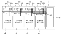
- the substrate polishing apparatus includes a housing 1, a load port 2, a polishing module 4A, a polishing module 4B, a polishing module 4C, a polishing module 4D, a first temporary mounting table 6, a second temporary mounting table 7, a third temporary mounting table 8, and a cleaning/drying section 9. , a first transport robot 11 , a second transport robot 12 , a third transport robot 13 , a fourth transport robot 14 , and a fifth transport robot 15 .
- Polishing module 4A, polishing module 4B, polishing module 4C, polishing module 4D, first temporary placement table 6, second temporary placement table 7, third temporary placement table 8, cleaning/drying unit 9, first transfer robot 11, second transfer robot 12 , a third transfer robot 13 , a fourth transfer robot 14 and a fifth transfer robot 15 are arranged in the housing 1 .
- Substrates to be polished such as wafers are accommodated in a substrate cassette 16 , and the substrate cassette 16 is placed on the load port 2 .
- the first transport robot 11 is arranged adjacent to the load port 2 .
- the first transfer robot 11 takes out the substrate to be polished from the substrate cassette 16 on the load port 2 and places it on the first temporary placement table 6 .
- the four polishing modules 4A-4D are arranged along the longitudinal direction of the housing 1.
- the four polishing modules 4A to 4D are arranged in a straight line when viewed from above the substrate polishing apparatus.
- Polishing module 4A is adjacent to polishing module 4B
- polishing module 4B is adjacent to polishing modules 4A and 4C
- polishing module 4C is adjacent to polishing modules 4B and 4D
- polishing module 4D is adjacent to polishing module 4C. next to.
- the polishing modules 4A-4D include three types of polishing modules: a notch polishing module for polishing the notch portion of the substrate, a bevel polishing module for polishing the bevel portion of the substrate, and a back surface polishing module for polishing the back surface of the substrate. .
- polishing modules 4A-4D are polishing modules that each polish a different area of the substrate. More specifically, the polishing module 4A and the polishing module 4B are notch polishing modules, the polishing module 4C is a bevel polishing module, and the polishing module 4D is a back side polishing module.
- the substrate polishing apparatus has four polishing modules 4A to 4D, but the substrate polishing apparatus includes a notch polishing module, a bevel polishing module, a back surface polishing module, and a device for polishing different regions of the substrate, respectively.
- the present embodiment is not limited as long as at least three polishing modules including at least three types of polishing modules among the four types of surface polishing modules are provided.
- a substrate polishing apparatus may include six polishing modules, including three types of polishing modules: two notch polishing modules, two bevel polishing modules, and two backside polishing modules.
- the polishing modules 4A to 4D are detachably arranged in the housing 1. Further, polishing modules 4A-4D have the same size. Therefore, the arrangement of the notch polishing modules, bevel polishing modules, and back surface polishing modules that constitute the polishing modules 4A to 4D can be changed.
- the polishing module 4A and the polishing module 4B may be a bevel polishing module
- the polishing module 4C may be a back surface polishing module
- the polishing module 4D may be a notch polishing module.
- the notch portion of the substrate is polished by at least one of the polishing module 4A and the polishing module 4B. Thereafter, the bevel portion of the substrate is polished by the polishing module 4C, and the back surface of the substrate is polished by the polishing module 4D.
- This processing flow that is, the types of polishing modules to be used and the order of operation of the polishing modules is an example, and the processing flow is not limited to this embodiment.
- the first temporary placement table 6 is a temporary placement table on which the substrate is temporarily placed before the substrate is polished by the polishing modules 4A to 4D.
- the first temporary placement table 6 may include a notch aligner (not shown).
- a notch aligner is a device for detecting a notch (notch) of a substrate and aligning the notch of the substrate with a predetermined position.
- the specific configuration of the notch aligner is not particularly limited as long as it can detect the notch of the substrate and align the notch of the substrate with a predetermined position.
- the second transfer robot 12 is arranged adjacent to the polishing module 4A and the polishing module 4B.
- the second transfer robot 12 takes out the substrate from the first temporary table 6, transfers the substrate to the polishing module 4A and/or the polishing module 4B, and receives the substrate from the polishing module 4A and/or the polishing module 4B. Further, the second transport robot 12 places the substrate polished by the polishing module 4A and/or the polishing module 4B on the second temporary placement table 7 .
- the second temporary placement table 7 is a temporary placement table on which the substrate is temporarily placed before the substrate is polished by the polishing module 4C.
- the third transfer robot 13 is arranged adjacent to the polishing modules 4C and 4D.
- the third transfer robot 13 takes out the substrate from the second temporary placement table 7, transfers the substrate to the polishing module 4C and the polishing module 4D, and receives the substrate from the polishing module 4C and the polishing module 4D. Further, the third transfer robot 13 places the substrates polished by the polishing modules 4C and 4D on the third temporary placement table 8.
- the third temporary placement table 8 is a temporary placement table on which the substrate is temporarily placed before the substrate is cleaned and dried by the cleaning/drying section 9 .
- the substrates polished by the polishing modules 4A to 4D are washed and dried by the washing/drying section 9.
- the cleaning/drying section 9 includes a first cleaning module 17 and a second cleaning module 18 for cleaning the substrates polished by the polishing modules 4A to 4D, and a drying module 19 for drying the cleaned substrates.
- the first cleaning module 17, the second cleaning module 18, and the drying module 19 are arranged along the longitudinal direction of the housing 1.
- the first cleaning module 17 is configured to perform scrub cleaning with a roll-shaped sponge member.
- the second cleaning module 18 is configured to perform scrub cleaning with a pencil-like sponge member.
- the washing/drying section 9 comprises a first washing module 17 and a second washing module 18, but in one embodiment, the washing/drying section 9 includes a first washing module 17 and a second washing module 18. may be provided with either one of
- the fourth transport robot 14 is arranged adjacent to the third temporary placement table 8 and between the first cleaning module 17 and the second cleaning module 18 .
- the fourth transport robot 14 takes out the substrate from the third temporary placement table 8 and transports it to the first cleaning module 17 of the cleaning/drying section 9 .
- the fourth transfer robot 14 transfers substrates between the first cleaning module 17 and the second cleaning module 18 .
- the fifth transfer robot 15 is arranged between the second cleaning module 18 and the drying module 19 .
- the fifth transport robot 15 transports substrates between the second cleaning module 18 and the drying module 19 .
- the substrates cleaned and dried by the cleaning/drying section 9 are returned to the substrate cassette 16 of the load port 2 by the first transfer robot 11 .
- the substrate polishing apparatus includes polishing modules 4A to 4D (more specifically, a notch polishing module, a bevel polishing module, and a back surface polishing module), a cleaning/drying section 9, a first transfer robot 11, a second transfer robot 12, a third An integrated control unit 20 electrically connected to the transport robot 13 , the fourth transport robot 14 , and the fifth transport robot 15 is further provided.
- polishing modules 4A to 4D more specifically, a notch polishing module, a bevel polishing module, and a back surface polishing module
- a cleaning/drying section 9 a first transfer robot 11, a second transfer robot 12, a third
- An integrated control unit 20 electrically connected to the transport robot 13 , the fourth transport robot 14 , and the fifth transport robot 15 is further provided.
- the integrated control unit 20 includes polishing modules 4A to 4D (more specifically, a notch polishing module, a bevel polishing module, and a back surface polishing module), a cleaning/drying unit 9, a first transfer robot 11, a second transfer robot 12, a second It is configured to control operations of the third transport robot 13 , the fourth transport robot 14 , and the fifth transport robot 15 .
- polishing modules 4A to 4D more specifically, a notch polishing module, a bevel polishing module, and a back surface polishing module
- a cleaning/drying unit 9 a first transfer robot 11, a second transfer robot 12, a second It is configured to control operations of the third transport robot 13 , the fourth transport robot 14 , and the fifth transport robot 15 .
- the integrated control unit 20 includes a storage device 20a that stores information such as the type of polishing module to be used and a program for creating a processing flow that is the operation order of the polishing modules, and an arithmetic device 20b that executes calculations according to the program. It has The storage device 20a includes a main storage device (for example, random access memory) accessible by the computing device 20b and an auxiliary storage device (for example, hard disk drive or solid state drive) for storing programs.
- the arithmetic device 20b includes a CPU (Central Processing Unit) or GPU (Graphic Processing Module) that performs calculations according to instructions included in programs stored in the storage device 20a.
- the integrated control unit 20 has at least one computer.
- the integrated control unit 20 may be an edge server connected to the substrate polishing apparatus via a communication line, or may be a cloud server connected to the substrate polishing apparatus via a network such as the Internet.
- the central control unit 20 may be a combination of multiple servers.
- the central control unit 20 may be a combination of an edge server and a cloud server connected to each other via a communication network such as the Internet or a local area network, or a combination of multiple servers not connected via a communication network.
- the specific configuration of the integrated control unit 20 is not limited to these examples.
- FIG. 2 is a side view of the substrate polishing apparatus shown in FIG. 1 as seen from the direction indicated by arrow A.
- the substrate polishing apparatus further comprises four control modules 30A-30D that control the operations of the polishing modules 4A-4D, respectively.
- Control module 30A is configured to control the operation of polishing module 4A.
- Control module 30B is configured to control the operation of polishing module 4B.
- Control module 30C is configured to control the operation of polishing module 4C.
- Control module 30D is configured to control the operation of polishing module 4D.
- the control modules 30A to 30D are electrically connected to the overall control section 20, and the overall control modules 30A to 30D are controlled by the overall control section 20.
- FIG. Control modules 30A-30D have the same size.
- the control modules 30A-30D are arranged in the housing 1 and arranged along the longitudinal direction of the housing 1.
- the four control modules 30A-30D are arranged in a straight line when viewed from above the substrate polishing apparatus.
- the control modules 30A-30D are arranged above the polishing modules 4A-4D, respectively.
- the control module 30A is arranged above the polishing module 4A
- the control module 30B is arranged above the polishing module 4B
- the control module 30C is arranged above the polishing module 4C.
- the control module 30D is arranged above the polishing module 4D.
- control module 30A and the control module 30B are notch polishing control modules that control the operation of the notch polishing module
- the control module 30C is a bevel polishing control module that controls the operation of the bevel polishing module
- Module 30D is a back polishing control module that controls the operation of the back polishing module.
- control modules 30A-30D are detachably arranged in the housing 1.
- Control modules 30A-30D are provided with wiring connectors 35A-35D, respectively.
- control module 30A includes wiring connector 35A
- control module 30B includes wiring connector 35B
- control module 30C includes wiring connector 35C
- control module 30D includes wiring connector 35C.
- a connector 35D is provided.
- the wiring connectors 35A-35D are connected to polishing module wirings 41A-41D for connecting the control modules 30A-30D and the polishing modules 4A-4D, respectively.
- the wiring connectors 35A-35D are further connected to main wirings 42A-42D for connecting the control modules 30A-30D and the integrated control unit 20, respectively.
- the wiring connector 35A is electrically connected to the polishing module 4A via the polishing module wiring 41A, and is further electrically connected to the integrated control section 20 via the main body wiring 42A.
- the wiring connector 35B is electrically connected to the polishing module 4B via the polishing module wiring 41B, and is further electrically connected to the integrated control section 20 via the main body wiring 42B.
- the wiring connector 35C is electrically connected to the polishing module 4C via the polishing module wiring 41C, and is further electrically connected to the integrated control section 20 via the main body wiring 42C.
- the wiring connector 35D is electrically connected to the polishing module 4D via the polishing module wiring 41D, and is further electrically connected to the integrated control section 20 via the main body wiring 42D.
- the polishing module wirings 41A to 41D are electrically connected to respective components of polishing modules 4A to 4D (notch polishing module, bevel polishing module, back surface polishing module), which will be described later. Therefore, by connecting the polishing module wirings 41A-41D to the wiring connectors 35A-35D, the polishing modules 4A-4D and the control modules 30A-30D can be electrically connected collectively.
- the main wirings 42A to 42D are electrically connected to the integrated control section 20. Therefore, by connecting the body wirings 42A-42D to the wiring connectors 35A-35D, the overall control section 20 and the control modules 30A-30D can be electrically connected collectively.
- control modules 30A to 30D can easily rearrange the arrangement of the control modules 30A to 30D together with the corresponding polishing modules 4A to 4D when rearranging the arrangement of the polishing modules 4A to 4D.
- FIG. 3 is a schematic diagram showing one embodiment of the notch polishing module.
- 4 is a plan view of the notch polishing module shown in FIG. 3.
- the notch polishing module is a device for polishing the notch portion N formed in the peripheral portion of the substrate W.
- the notch polishing module includes a polishing head 103, a substrate holding section 105, a substrate swing section 110, a polishing tape supply mechanism 120, a liquid supply nozzle 130, a notch detection mechanism 140, a polishing head movement mechanism 150, and a tilt A mechanism 170 is provided.
- the substrate holding unit 105 holds and rotates the substrate W to be polished.
- the substrate holding unit 105 includes a holding stage 107 that holds the substrate W by vacuum adsorption, a first shaft 108 that is connected to the center of the holding stage 107, and a holding stage drive mechanism that rotates and moves the holding stage 107 up and down. 109 is provided.
- the holding stage drive mechanism 109 is configured to rotate the holding stage 107 about its axis Cr and move it vertically along the axis Cr.
- the substrate W is placed on the substrate holding surface of the holding stage 107 by the second transfer robot 12 (see FIG. 1) so that the center O1 of the substrate W is positioned on the axis Cr of the holding stage 107.
- the substrate holding unit 105 can rotate the substrate W about the axis Cr of the holding stage 107 (that is, the axis of the substrate W) and move the substrate W up and down along the axis Cr of the holding stage 107 . .
- the substrate swing unit 110 rotates (that is, swings) the substrate W by a predetermined angle in the horizontal plane clockwise and counterclockwise around the notch portion N of the substrate W.
- the substrate swing unit 110 includes a swing arm 112 connected to the holding stage drive mechanism 109, a second shaft 113 connected to the swing arm 112, and a swing mechanism 114 that swings the swing arm 112.
- the second shaft 113 extends through the base plate 160 .
- the substrate holding portion 105 and the second shaft 113 are connected via the swing arm 112 .
- the swing mechanism 114 rotates the second shaft 113 clockwise and counterclockwise by a predetermined angle.
- the substrate holder 105 also rotates clockwise and counterclockwise.
- the axial center of the first shaft 108 is deviated from the axial center of the second shaft 113, and the notch portion N of the substrate W held by the holding stage 107 is positioned on the extension of the axial center of the second shaft 113.
- the substrate W on the holding stage 107 is rotated by the swing mechanism 114 around the notch portion N by a predetermined angle clockwise and counterclockwise in the horizontal plane (that is, swinging). is done).
- the polishing tape supply mechanism 120 supplies the polishing tape 102 to the polishing head 103 and recovers it from the polishing head 103 .
- the polishing tape supply mechanism 120 includes a tape take-up reel 121 that supplies the polishing tape 102 to the polishing head 103 and a tape take-up reel 122 that collects the polishing tape 102 used for polishing the substrate W.
- Tension motors (not shown) are connected to the tape feed reel 121 and the tape take-up reel 122, respectively.
- the tape feed reel 121 and tape take-up reel 122 are fixed to a reel base 128 via a tension motor. Each tension motor can apply a predetermined torque to the tape take-up reel 121 and the tape take-up reel 122 to apply a predetermined tension to the polishing tape 102 .
- the polishing tape supply mechanism 120 further includes a plurality of guide rollers 124, 125, 126, 127 for supporting the polishing tape 102.
- Guide rollers 124 , 125 , 126 , 127 are fixed to reel base 128 .
- the polishing tape 102 is supplied to the polishing head 103 so that the polishing surface of the polishing tape 102 faces the notch portion N of the substrate W. As shown in FIG. The advancing direction of the polishing tape 102 is guided by guide rollers 124 , 125 , 126 and 127 .
- the liquid supply nozzle 130 is configured to supply the liquid toward the notch portion N of the substrate W.
- An example of the liquid supplied to the substrate W is pure water.
- liquid is supplied from the liquid supply nozzle 130 toward the notch portion N of the substrate W.
- Liquid supply nozzle 130 is coupled to swing arm 112 of swing mechanism 114 . Therefore, the liquid supply nozzle 130 is rotated (that is, swung) clockwise and counterclockwise around the notch portion N of the substrate W by a predetermined angle in the horizontal plane by the swing mechanism 114 integrally with the substrate holding portion 105 . ).
- the notch detection mechanism 140 is configured to detect the notch portion N formed on the substrate W.
- the holding stage 107 rotates so that the notch portion N faces the polishing head 103 .
- the notch detection mechanism 140 detects the notch portion N before polishing and performs alignment.
- the polishing head moving mechanism 150 has a guide rail 154 extending in the same direction as the line connecting the center of the substrate W on the holding stage 107 and the notch portion N. Guide rail 154 is fixed to base plate 160 .
- the polishing head 103 and the reel base 128 of the polishing tape supply mechanism 120 are connected to the polishing head moving mechanism 150 via a movable plate 152 .
- the entirety of the polishing head 103 and the polishing tape supply mechanism 120 can move together with the movable plate 152 .
- the polishing head moving mechanism 150 has an air cylinder 155 connected to a movable plate 152 via a connecting shaft 156 .
- Air cylinder 155 is fixed to base plate 160 .
- the polishing head moving mechanism 150 drives the air cylinder 155 to move the movable plate 152 along the guide rail 154, thereby bringing the polishing head 103 and the polishing tape supply mechanism 120 closer to the notch portion N of the substrate W and Separate.
- the tilt mechanism 170 is configured to tilt the polishing head 103 with respect to the substrate holding surface of the holding stage 107 . More specifically, the tilt mechanism 170 has a crank arm 172 connected to the polishing head 103 and an arm rotating device 173 that rotates the crank arm 172 . One end of the crank arm 172 is positioned substantially at the same height as the substrate holding surface of the holding stage 107 and connected to an arm rotating device 173 . The other end of crank arm 172 is connected to polishing head 103 .
- the entire polishing head 103 can be tilted around the notch portion N of the substrate W on the substrate holding surface of the holding stage 107 .
- the tilt mechanism 170 is configured to maintain the polishing head 103 at a predetermined tilt angle. As long as the polishing head 103 can be tilted with respect to the substrate holding surface of the holding stage 107 and the substrate W, the specific configuration of the tilt mechanism 170 is not limited to the embodiment shown in FIG.
- the notch polishing module is electrically connected to a notch polishing control module that controls the operation of each component of the notch polishing module. Since this notch polishing control module corresponds to the control modules 30A and 30B shown in FIG. 2, the notch polishing control module is denoted by reference numeral 30A in the following description.
- the substrate holding unit 105, substrate swing unit 110, polishing tape supply mechanism 120, liquid supply nozzle 130, notch detection mechanism 140, polishing head movement mechanism 150, and tilt mechanism 170 are electrically connected to the notch polishing control module 30A.
- the operations of the substrate holding section 105, substrate swing section 110, polishing tape supply mechanism 120, liquid supply nozzle 130, notch detection mechanism 140, polishing head movement mechanism 150, and tilt mechanism 170 are controlled by the notch polishing control module 30A.
- the notch polishing control module 30A has at least one computer.
- the notch polishing control module 30A includes a storage device 180a storing programs, and an arithmetic device 180b that executes operations according to the programs.
- the storage device 180a includes a main storage device (eg, random access memory) accessible by the computing device 180b and an auxiliary storage device (eg, hard disk drive or solid state drive) for storing programs.
- Arithmetic device 180b includes a CPU (Central Processing Unit) or GPU (Graphic Processing Module) that performs calculations according to instructions included in programs stored in storage device 180a.
- the specific configuration of the notch polishing control module 30A is not limited to these examples.
- the polishing of the notch portion N of the substrate W is performed as follows.
- the holding stage 107 is raised, and the substrate W is placed on the substrate holding surface of the holding stage 107 and held by vacuum suction.
- the notch detection mechanism 140 detects the position of the notch portion N of the substrate W, and the substrate holding portion 105 lowers the substrate W to the polishing position so that the notch portion N faces the polishing head 103 .
- the holding stage 107 is rotated. Furthermore, liquid supply from the liquid supply nozzle 130 is started.
- the polishing head moving mechanism 150 brings the polishing head 103 close to the notch portion N of the substrate W, and the polishing head 103 brings the polishing surface of the polishing tape 102 into sliding contact with the notch portion N for polishing.
- the substrate swing section 110 swings the substrate W about the notch portion N, and the tilt mechanism 170 tilts the polishing head 103 about the notch portion N. As shown in FIG.
- the notch polishing control module 30A issues a command to the notch polishing module to finish polishing the substrate W. Specifically, the notch polishing control module 30A stops the operations of the substrate swing section 110 and the tilt mechanism 170, and separates the polishing head 103 from the substrate W by the polishing head moving mechanism 150. FIG. After that, the notch polishing control module 30A stops the operations of the substrate holder 105, the polishing tape supply mechanism 120, and the liquid supply nozzle 130, and finishes the polishing of the substrate W. FIG.
- the specific configuration of the notch polishing module is not limited to the above embodiment as long as the notch portion N of the substrate W can be polished.
- FIG. 5 is a schematic diagram showing one embodiment of the bevel polishing module.
- the bevel polishing module is an apparatus for polishing the peripheral portion of the substrate W including the bevel portion B.
- the bevel polishing module includes a polishing head 203, a substrate holder 205, a polishing tape supply mechanism 220, a lower supply nozzle 231, an upper supply nozzle 232, and a tilt mechanism (not shown). .
- the substrate holding part 205 holds and rotates the substrate W.
- the substrate holding section 205 has a holding stage 207 , a shaft 208 and a holding stage driving mechanism 209 .
- the holding stage 207, shaft 208, and holding stage drive mechanism 209 have the same configurations as the holding stage 107, first shaft 108, and holding stage drive mechanism 109 of the notch polishing module described with reference to FIG. Therefore, redundant explanations are omitted.
- the polishing tape supply mechanism 220 supplies the polishing tape 202 to the polishing head 203 and recovers it from the polishing head 203 .
- the polishing tape supply mechanism 220 includes a tape supply reel 221, a tape take-up reel 222, and a plurality of guide rollers 224,225,226,227.
- a tape take-up reel 221 , a tape take-up reel 222 and a plurality of guide rollers 224 , 225 , 226 and 227 are fixed to a reel base 228 .
- the polishing tape 202 is supplied to the polishing head 203 so that the polishing surface of the polishing tape 202 faces the bevel portion B of the substrate W. As shown in FIG.
- the configuration of the tape take-up reel 221, the tape take-up reel 222, and the plurality of guide rollers 224, 225, 226, 227 is similar to that of the tape take-up reel 121, tape take-up reel of the notch polishing module described with reference to FIG. 122, and a plurality of guide rollers 124, 125, 126, 127, redundant description thereof will be omitted.
- the lower supply nozzle 231 is configured to supply liquid to the lower surface of the substrate W.
- the upper supply nozzle 232 is configured to supply the upper surface of the substrate W with liquid.
- An example of the liquid supplied to the substrate W is pure water.
- the polishing head 203 includes a pressing member 242 that presses the polishing surface of the polishing tape 202 against the bevel portion B of the substrate W, and an air cylinder (driving mechanism) 245 that moves the pressing member 242 toward the bevel portion B of the substrate W. and By controlling the air pressure supplied to the air cylinder 245, the pressing force of the polishing tape 202 against the substrate W is adjusted.
- the pressing member 242 is arranged on the back side of the polishing tape 202 (the back side of the polishing surface having abrasive grains).
- the tilt mechanism (not shown) has the same configuration as the tilt mechanism 170 of the notch polishing module described with reference to FIG. 4, so redundant description thereof will be omitted.
- the tilt mechanism of the bevel polishing module is configured to tilt the polishing head 203 with respect to the substrate holding surface of the holding stage 207 .
- the bevel polishing module is electrically connected to a bevel polishing control module that controls the operation of each component of the bevel polishing module. Since this bevel polishing control module corresponds to the control module 30C shown in FIG. 2, the reference numeral 30C is attached to the bevel polishing control module in the following description.
- the substrate holder 205, polishing tape supply mechanism 220, lower supply nozzle 231, upper supply nozzle 232, air cylinder 245 and tilt mechanism are electrically connected to the bevel polishing control module 30C. Operations of the substrate holder 205, the polishing tape supply mechanism 220, the lower supply nozzle 231, the upper supply nozzle 232, the air cylinder 245 and the tilt mechanism are controlled by the bevel polishing control module 30C.
- the bevel polishing control module 30C has a storage device 280a and an arithmetic device 280b. Since the storage device 280a and the arithmetic device 280b have the same basic configuration as the storage device 180a and the arithmetic device 180b of the notch polishing control module 30A described above, redundant description thereof will be omitted.
- the polishing of the bevel portion B of the substrate W is performed as follows.
- the holding stage 207 is raised, and the substrate W is placed on the substrate holding surface of the holding stage 207 and held by vacuum suction.
- the substrate holder 205 lowers the substrate W to the polishing position and rotates the holding stage 207 . Furthermore, liquid supply is started from the lower supply nozzle 231 and the upper supply nozzle 232 .
- the air cylinder 245 is driven to press the pressing member 242 of the polishing head 203 against the bevel portion B of the substrate W, and the bevel portion B of the substrate W is polished.
- the tilt mechanism tilts the polishing head 203 with respect to the substrate holding surface of the holding stage 207 .
- the bevel polishing control module 30C issues a command to the bevel polishing module to finish polishing the substrate W. Specifically, the bevel polishing control module 30C stops the operation of the tilt mechanism, stops driving the air cylinder 245 of the polishing head 203, and separates the pressing member 242 from the substrate W. FIG. After that, the bevel polishing control module 30C stops the operations of the substrate holder 205, the polishing tape supply mechanism 220, the lower supply nozzle 231, and the upper supply nozzle 232, and finishes the polishing of the substrate W.
- the specific configuration of the bevel polishing module is not limited to the above embodiment as long as the bevel portion B of the substrate W can be polished.
- FIG. 6 is a schematic diagram showing one embodiment of the back polishing module.
- the back surface polishing module is a device for polishing the back surface of the substrate W.
- the back surface polishing module includes a polishing head 303 , a substrate holder 305 , a polishing tape supply mechanism 320 , a rinse liquid supply nozzle 331 , a protective liquid supply nozzle 332 and a polishing head moving mechanism 350 .
- the substrate holding unit 305 includes a plurality of rollers 308 that can come into contact with the peripheral edge of the substrate W, and a roller rotation mechanism (not shown) that rotates the plurality of rollers 308 around their respective axes.
- the polishing head 303 is arranged below the substrate W held by the substrate holding part 305 .
- illustration of part of the substrate holding part 305 is omitted.
- the substrate holder 305 of this embodiment comprises four rollers 308 (two of which are not shown).
- the first surface S1 of the substrate W is the back surface of the substrate W on which no devices are formed or devices are not to be formed, ie, the non-device surface.
- a second side S2 of the substrate W, opposite the first side S1, is the side on which the devices are or are to be formed, ie the device side.
- the substrate W is horizontally held by the substrate holder 305 with the first surface S1 facing downward.
- the roller rotation mechanism is configured to rotate the four rollers 308 in the same direction at the same speed.
- the peripheral edge of the substrate W is gripped by the rollers 308 .
- the substrate W is held horizontally, and the rotation of the roller 308 causes the substrate W to rotate about its axis.
- the four rollers 308 rotate about their respective axes, but the position of the rollers 308 themselves remains stationary.
- the polishing tape supply mechanism 320 supplies the polishing tape 302 to the polishing head 303 and recovers it from the polishing head 303 .
- the polishing tape supply mechanism 320 includes a tape take-up reel 321 that supplies the polishing tape 302 to the polishing head 303 and a tape take-up reel 322 that collects the polishing tape 302 used for polishing the substrate W.
- Tension motors (not shown) are connected to the tape feed reel 321 and the tape take-up reel 322, respectively.
- the tape feed reel 321 and tape take-up reel 322 are fixed to a reel base 328 via a tension motor, and the reel base 328 is fixed to a movable plate 340 .
- Each tension motor can apply a predetermined torque to the tape take-up reel 321 and the tape take-up reel 322 to apply a predetermined tension to the polishing tape 302 .
- the polishing tape supply mechanism 320 further includes a plurality of guide rollers 324 , 325 , 326 and 327 for supporting the polishing tape 302 .
- the polishing tape 302 is supplied to the polishing head 303 so that the polishing surface of the polishing tape 302 faces the first surface S1 of the substrate W.
- Guide rollers 324 , 325 , 326 , 327 are fixed to a holding member (not shown), and this holding member is fixed to movable plate 340 .
- the advancing direction of the polishing tape 302 is guided by guide rollers 324 , 325 , 326 and 327 so as to surround the polishing head 303 . More specifically, guide rollers 325 and 326 arranged above the polishing head 303 guide the polishing tape 302 so that the polishing tape 302 advances in a direction parallel to the first surface S1 of the substrate W.
- the rinse liquid supply nozzle 331 is arranged below the substrate W held by the substrate holder 305 and configured to supply the rinse liquid toward the processing point on the first surface S1 of the substrate W.
- Examples of the rinsing liquid supplied to the first surface S1 of the substrate W include, for example, pure water or an alkaline chemical liquid.
- the protective liquid supply nozzle 332 is arranged above the substrate W held by the substrate holder 305 and configured to supply the second surface S2 of the substrate W with the protective liquid.
- An example of the protective liquid supplied to the second surface S2 of the substrate W is pure water.
- the polishing head moving mechanism 350 is configured to move the polishing head 303 between the center O1 of the first surface S1 of the substrate W and the outermost portion of the first surface S1.
- the polishing head moving mechanism 350 has a plurality of linear motion guides 355 on the lower surface of the movable plate 340 , and the movable plate 340 is supported by the plurality of linear motion guides 355 .
- a plurality of linear motion guides 355 are arranged on the base plate 360 .
- the linear motion guide 355 limits the motion of the movable plate 340 to linear motion of the substrate W in the radial direction.
- the polishing head 303 , the reel base 328 of the polishing tape supply mechanism 320 , and the holding member to which the guide rollers 324 , 325 , 326 and 327 are fixed are connected to the polishing head moving mechanism 350 via the movable plate 340 .
- the entire polishing head 303 and polishing tape supply mechanism 320 are movable together with the movable plate 340 .
- the polishing head moving mechanism 350 has a ball screw mechanism 352 connected to the movable plate 340 .
- Ball screw mechanism 352 is fixed to base plate 360 .
- the polishing head moving mechanism 350 moves the polishing head 303 and the polishing tape supply mechanism 320 in the radial direction of the substrate W relative to the substrate holder 305 by driving the ball screw mechanism 352 .
- the polishing head moving mechanism 350 moves the polishing head 303 between the center O1 of the first surface S1 of the substrate W and the outermost portion of the first surface S1.
- the polishing head 303 is supported by a support member 343 , and the support member 343 is fixed to the movable plate 340 . Therefore, the entire polishing head 303 can move together with the movable plate 340 .
- the support member 343 has a through hole (not shown) through which the polishing tape 302 extends.
- the polishing head 303 includes a pressing member 342 that presses the polishing surface of the polishing tape 302 against the first surface S1 of the substrate W, and an air cylinder (which moves the pressing member 342 toward the first surface S1 of the substrate W). drive mechanism) 345. By controlling the air pressure supplied to the air cylinder 345, the pressing force of the polishing tape 302 against the substrate W is adjusted.
- the pressing member 342 is arranged on the back side of the polishing tape 302 (the back side of the polishing surface having abrasive grains).
- the back polishing module is electrically connected to a back polishing control module that controls the operation of each component of the back polishing module. Since this back surface polishing control module corresponds to the control module 30D shown in FIG. 2, the back surface polishing control module is denoted by reference numeral 30D in the following description.
- the substrate holder 305, the polishing tape supply mechanism 320, the rinse liquid supply nozzle 331, the protective liquid supply nozzle 332, the polishing head moving mechanism 350, and the air cylinder 345 of the polishing head 303 are electrically connected to the back surface polishing control module 30D. ing.
- the back surface polishing control module 30D has a storage device 380a and an arithmetic device 380b. Since the storage device 380a and the arithmetic device 380b have the same basic configuration as the storage device 180a and the arithmetic device 180b of the notch polishing control module 30A described above, redundant description thereof will be omitted.
- the polishing of the first surface S1 of the substrate W is performed as follows.
- the substrate holding unit 305 holds the substrate W with the first surface S1 facing downward by the rollers 308, Rotate around the axis of W. Further, supply of the rinse liquid to the first surface S1 of the substrate W from the rinse liquid supply nozzle 331 is started, and supply of the protective liquid to the second surface S2 of the substrate W from the protective liquid supply nozzle 332 is started.
- the polishing head moving mechanism 350 moves the polishing head 303 below the center O1 of the first surface S1 of the substrate W. While the polishing head moving mechanism 350 moves the polishing head 303 and the polishing tape supply mechanism 320 radially outward of the substrate W, the air cylinder 345 is driven to move the pressing member 342 of the polishing head 303 to the first surface S1 of the substrate W. , the first surface S1 of the substrate W is polished.
- the back surface polishing control module 30D issues a command to the rear surface polishing module to finish polishing the substrate W.
- the back surface polishing control module 30D stops the operation of the polishing head moving mechanism 350, stops driving the air cylinder 345 of the polishing head 303, lowers the pressing member 342, and moves the polishing tape 302 onto the substrate W. It is separated from the first surface S1.
- the back surface polishing control module 30D stops the operations of the substrate holding unit 305, the polishing tape supply mechanism 320, the rinse liquid supply nozzle 331, and the protective liquid supply nozzle 332, and finishes the polishing of the substrate W.
- the polishing head moving mechanism 350 may reciprocate the polishing head 303 between the outermost portion of the first surface S1 of the substrate W and the center O1.
- the specific configuration of the back surface polishing module is not limited to the above embodiment as long as it can polish the back surface (first surface S1) of the substrate W.
- FIG. 7 is a diagram showing an example of the processing flow of the substrate polishing apparatus according to this embodiment.
- the notch portion N of the substrate W is polished by the polishing module 4A or the polishing module 4B which is the notch polishing module
- the bevel portion B of the substrate W is polished by the polishing module 4C which is the bevel polishing module
- the back side polishing module is polished.
- the rear surface (first surface S1) of the substrate W is polished by the polishing module 4D.
- the polished substrate W is cleaned by the first cleaning module 17 , further cleaned by the second cleaning module 18 , and then dried by the drying module 19 .
- the polishing time of the notch portion N by the notch polishing module is 2T (twice the time unit T), the polishing time of the bevel portion B by the bevel polishing module is 1T, and the rear surface is polished.
- the polishing time of the rear surface by the module is 1T.
- the cleaning time by the first cleaning module 17 and the second cleaning module 18 and the drying time by the drying module 19 are each 1T.
- FIG. 7 shows the processing flow of the first substrate W1 to be processed first and the second substrate W2 to be processed next.
- the time represents the time elapsed from the start of polishing of the first substrate W1.
- the notch portion N of the first substrate W1 is polished by the polishing module 4A (that is, the notch polishing module) from time 0 to time 2T.
- the bevel portion B of the first substrate W1 is polished by the polishing module 4C (that is, the bevel polishing module) from time 2T to time 3T.
- step S103 from time 3T to time 4T, the back surface (first surface S1) of the first substrate W1 is polished by the polishing module 4D (that is, the back surface polishing module).
- step S104 the first cleaning module 17 cleans the polished first substrate W1 from time 4T to time 5T.
- step S105 the first substrate W1 cleaned by the first cleaning module 17 is cleaned by the second cleaning module 18 from time 5T to time 6T.
- step S106 the first substrate W1 cleaned by the second cleaning module 18 is dried by the drying module 19 from time 6T to time 7T.
- step S107 the notch portion N of the second substrate W2 is polished by the polishing module 4B (that is, the notch polishing module) from time 1T to time 3T.
- step S108 the bevel portion B of the second substrate W2 is polished by the polishing module 4C (that is, the bevel polishing module) from time 3T to time 4T.
- step S109 the back surface (first surface S1) of the second substrate W2 is polished by the polishing module 4D (that is, the back surface polishing module) from time 4T to time 5T.
- step S110 the polished second substrate W2 is cleaned in the first cleaning module 17 from time 5T to time 6T.
- step S111 the second substrate W2 cleaned by the first cleaning module 17 is cleaned by the second cleaning module 18 from time 6T to time 7T.
- step S112 the second substrate W2 cleaned by the second cleaning module 18 is dried by the drying module 19 from time 7T to time 8T.
- the substrate polishing apparatus has the notch polishing module, the bevel polishing module, and the back surface polishing module in the same housing 1, so that polishing can be continuously performed by different types of polishing modules. . Therefore, it is not necessary to wash and dry the substrate W each time polishing by each polishing module is completed, and the entire processing time can be shortened.
- the substrate polishing apparatus includes a polishing module 4A and a polishing module 4B, which are notch polishing modules having a longer polishing time than other processes. Therefore, the notch portions N of the first substrate W1 and the second substrate W2 can be polished in parallel by the polishing module 4A and the polishing module 4B. Therefore, in the next bevel polishing module, the second substrate W2 can be polished immediately after polishing the first substrate W1 without any idle time. This can shorten the overall processing time when processing a plurality of substrates.
- the processing flow described above is an example, and in one embodiment, the processing flow is such that after the bevel portion B is polished by the polishing module 4C, which is the bevel polishing module, the back surface (first polishing) is performed by the polishing module 4D, which is the back surface polishing module.
- the surface S1) may be polished, and then the notch portion N of the substrate W may be polished by the polishing module 4A or the polishing module 4B, which is a notch polishing module.
- the substrate polishing apparatus can change the type and arrangement of the polishing modules 4A to 4D according to the processing flow and the polishing time in each polishing module. Therefore, one substrate polishing apparatus can handle various polishing processes and realize an efficient processing flow.
- the substrate polishing apparatus may comprise two first cleaning modules 17 , two second cleaning modules 18 and two drying modules 19 .
- two first cleaning modules 17, two second cleaning modules 18, and two drying modules 19 concurrently clean and dry a plurality of substrates polished by the polishing modules 4A to 4D. you can go
- FIG. 8 is a schematic diagram showing another embodiment of the substrate polishing apparatus. The details of this embodiment that are not particularly described are the same as those of the above-described embodiment described with reference to FIGS.
- the control modules 30A-30D of the substrate polishing apparatus shown in FIG. 8 are provided with abnormality detection systems 50A-50D for detecting abnormalities occurring in the corresponding polishing modules 4A-4D.
- anomaly detection systems 50A-50D can detect an anomaly based on various signals obtained from the polishing modules 4A-4D.
- an anomaly detection system having known anomaly detection means can be used.
- One abnormality detection system 50A to 50D of the present embodiment is provided for each of the polishing modules 4A to 4D. It may be configured to detect anomalies in the polishing modules 4A-4D.
- the abnormality detection system 50A is configured to detect an abnormality occurring in the polishing module 4A whose operation is controlled by the control module 30A.
- the anomaly detection system 50B is configured to detect an anomaly occurring in the polishing module 4B whose operation is controlled by the control module 30B.
- the anomaly detection system 50C is configured to detect anomalies occurring in the polishing module 4C whose operation is controlled by the control module 30C.
- Anomaly detection system 50D is configured to detect anomalies occurring in polishing module 4D whose operation is controlled by control module 30D.
- the control modules 30A to 30D send an abnormality detection signal to the integrated control section 20.
- the overall control unit 20 is configured to create a processing flow that does not use the polishing module in which an abnormality has been detected, if the polishing module is of a type in which a plurality of polishing modules in which an abnormality has been detected are provided.
- FIG. 9 is a diagram showing the processing flow before abnormality detection. Similar to the embodiment described with reference to FIG. 7, polishing of the notch portions N of a plurality of substrates is performed in parallel by two notch polishing modules, polishing module 4A and polishing module 4B.
- FIG. 10 is a diagram showing a modified processing flow after detection of an abnormality in the polishing module 4B.
- the control module 30B sends an abnormality detection signal to the integrated control section 20.
- the integrated control unit 20 creates a processing flow that does not use the polishing module 4B, uses the polishing module 4A from the processing flow of FIG. 9 that uses both the polishing modules 4A and 4B, and Change to the processing flow of FIG. 10 that does not use the polishing module 4B.
- the type of polishing module 4B in which an abnormality is detected is a plurality of notch polishing modules. Therefore, when an abnormality occurs in the polishing module 4B, by changing the processing flow to polishing the notch portion N using only the polishing module 4A, the substrate can be polished without stopping the operation of the entire substrate polishing apparatus. Processing can continue.
- the substrate polishing apparatus of the present embodiment is provided with two notch polishing modules, in one embodiment, three or more notch polishing modules are provided, and the abnormality detection system detects three or more notch polishing modules.
- the overall control unit 20 may change the processing flow to one that does not use the at least one notch polishing module in which the abnormality is detected.
- the substrate polishing apparatus is provided with a plurality of bevel polishing modules or back surface polishing modules, and when an abnormality in the plurality of bevel polishing modules or back surface polishing modules is detected by the abnormality detection system, the integrated control unit 20 may change the processing flow to one that does not use the bevel polishing module or the back surface polishing module in which the abnormality is detected.
- the substrate polishing apparatus described above includes three types of polishing modules, a notch polishing module, a bevel polishing module, and a back surface polishing module
- the configuration of the substrate polishing apparatus is not limited to these types of polishing modules.
- the polishing module may be a polishing module using a whetstone instead of a polishing tape as a polishing tool, or a polishing module (CMP module) using a polishing pad (for example, non-woven fabric) as a polishing tool in the presence of a polishing liquid (slurry). ) and so on.
- FIG. 11 is a schematic diagram showing still another embodiment of the substrate polishing apparatus. Since the configuration and operation of this embodiment, which are not particularly described, are the same as those of the above-described embodiments, redundant description thereof will be omitted.
- the polishing modules 4A and 4B are device surface polishing modules for polishing the device surface of the substrate instead of the notch polishing modules.
- the control modules 30A and 30B are device surface polishing control modules that control the operation of the device surface polishing modules.
- the polishing modules 4A to 4D are detachably arranged in the housing 1. Further, polishing modules 4A-4D have the same size. Therefore, the arrangement of the device side polishing module, the bevel polishing module, and the back side polishing module that constitute the polishing modules 4A to 4D can be changed.
- the polishing module 4A and the polishing module 4B may be the bevel polishing module
- the polishing module 4C may be the back surface polishing module
- the polishing module 4D may be the device surface polishing module.
- the device surface of the substrate is polished by at least one of the polishing modules 4A and 4B. Thereafter, the bevel portion of the substrate is polished by the polishing module 4C, and the back surface of the substrate is polished by the polishing module 4D.
- This processing flow that is, the types of polishing modules to be used and the order of operation of the polishing modules is an example, and the processing flow is not limited to this embodiment.
- FIG. 12 is a schematic diagram showing one embodiment of the device surface polishing module.
- the device surface polishing module is an apparatus for polishing the device surface of the substrate W.
- the device surface polishing module includes a buff table 403 , buff head 405 , liquid supply nozzle 410 , table motor 415 , buff head shaft 418 , support shaft 420 and buff arm 421 .
- the buff table 403 is configured to hold the device surface of the substrate W facing upward.
- the first side S1 of the substrate W is the back side of the substrate W on which no devices are formed or devices are not to be formed, ie, the non-device side.
- a second side S2 of the substrate W, opposite the first side S1, is the side on which the devices are or are to be formed, ie the device side.
- the substrate W is held horizontally on the buffing table 403 with its second surface S2 facing upward.
- the buffing table 403 is connected to a table motor 415 arranged below it via a table shaft 403a.
- the table motor 415 is configured to rotate the buffing table 403 and the substrate W in the direction indicated by the arrow in FIG. 12 around the table shaft 403a.
- the buff head 405 is configured to hold the buff pad 401 on its lower surface.
- the diameter of the buff pad 401 is smaller than the diameter of the substrate W, as shown in FIG.
- the lower surface of the buff pad 401 constitutes a polishing surface 401a for polishing the substrate W.
- the buff head 405 is fixed to the lower end of the buff head shaft 418 and is rotatable together with the buff head shaft 418 .
- the buff head shaft 418 is connected to the buff arm 421 and is connected to a head rotation mechanism (not shown) arranged inside the buff arm 421 .
- the head rotation mechanism is configured to rotate the buffing head shaft 418 and the buffing head 405 in the directions indicated by the arrows in FIG.
- the buff head shaft 418 is connected to a head vertical movement mechanism (not shown) arranged inside the buff arm 421 .
- the head vertical motion mechanism is configured to relatively move the buff head shaft 418 and the buff head 405 vertically with respect to the buff arm 421 .
- the buff arm 421 is connected to the upper end of the support shaft 420 and is connected to an arm turning mechanism (not shown) disposed within the support shaft 420 .
- the arm turning mechanism is configured to turn the buff arm 421 about the support shaft 420 . By turning the buff arm 421 , the buff head shaft 418 and the buff head 405 can be moved between above the buff table 403 and outside the buff table 403 .
- the liquid supply nozzle 410 is arranged above the buff table 403 .
- the liquid supply nozzle 410 is configured to supply liquid toward the second surface S2 of the substrate W held on the buff table 403 .
- Examples of the liquid supplied to the second surface S2 of the substrate W include pure water and chemical liquid (for example, slurry).
- the device surface polishing module is electrically connected to a device surface polishing control module that controls the operation of each component of the device surface polishing module. Since this device surface polishing control module corresponds to the control modules 30A and 30B shown in FIG. 11, the device surface polishing control module is denoted by reference numeral 30A in the following description.
- the table motor 415, head rotation mechanism, head vertical movement mechanism, arm rotation mechanism, and liquid supply nozzle 410 are electrically connected to the device surface polishing control module 30A. The operations of the table motor 415, head rotation mechanism, head vertical movement mechanism, arm rotation mechanism, and liquid supply nozzle 410 are controlled by the device surface polishing control module 30A.
- the device surface polishing control module 30A includes a storage device 480a and an arithmetic device 480b. Since the storage device 480a and the arithmetic device 480b have the same basic configuration as the storage device 180a and the arithmetic device 180b of the notch polishing control module 30A described above, redundant description thereof will be
- the polishing of the second surface S2 of the substrate W is performed as follows.
- the buff table 403 holds the substrate W with its second surface S2 facing upward.
- the table motor 415 rotates the substrate W held on the buffing table 403 around the table shaft 403a.
- supply of liquid (for example, slurry) from the liquid supply nozzle 410 toward the second surface S2 of the substrate W is started.
- the polishing surface 401a of the buffing pad 401 held by the buffing head 405 is pressed against the second surface S2 of the substrate W by the head vertical movement mechanism, whereby the second surface S2 of the substrate W is polished. be.
- the device surface polishing control module 30A issues a command to the device surface polishing module to finish polishing the substrate W. Specifically, the device surface polishing control module 30A issues a command to the head vertical movement mechanism to separate the buffing head 405 from the substrate W. FIG. After that, the device surface polishing control module 30A stops the operation of the table motor 415 and the liquid supply nozzle 410 to finish the polishing of the substrate W.
- the specific configuration of the device surface polishing module is not limited to the above embodiment as long as the device surface (second surface S2) of the substrate W can be polished.
- FIG. 13 is a diagram showing an example of the processing flow of the substrate polishing apparatus according to this embodiment.
- the device surface (second surface S2) of the substrate W is polished by the polishing module 4A or the polishing module 4B, which is the device surface polishing module, and the bevel portion B of the substrate W is polished by the polishing module 4C, which is the bevel polishing module. is polished, and the rear surface (first surface S1) of the substrate W is polished by the polishing module 4D, which is a rear surface polishing module.
- the polished substrate W is cleaned by the first cleaning module 17 , further cleaned by the second cleaning module 18 , and then dried by the drying module 19 .
- the device surface polishing time by the device surface polishing module is 2T (twice the time unit T)
- the bevel portion B polishing time by the bevel polishing module is 1T
- the back surface polishing is 1T
- the cleaning time by the first cleaning module 17 and the second cleaning module 18 and the drying time by the drying module 19 are each 1T.
- FIG. 13 shows the processing flow of the first substrate W1 to be processed first and the second substrate W2 to be processed next.
- the time represents the time elapsed from the start of polishing of the first substrate W1.
- the device surface (second surface S2) of the first substrate W1 is polished by the polishing module 4A (that is, the device surface polishing module) from time 0 to time 2T.
- the bevel portion B of the first substrate W1 is polished by the polishing module 4C (that is, the bevel polishing module) from time 2T to time 3T.
- the back surface (first surface S1) of the first substrate W1 is polished by the polishing module 4D (that is, the back surface polishing module).
- step S204 the first cleaning module 17 cleans the polished first substrate W1 from time 4T to time 5T.
- step S205 the first substrate W1 cleaned by the first cleaning module 17 is cleaned by the second cleaning module 18 from time 5T to time 6T.
- step S206 the first substrate W1 cleaned by the second cleaning module 18 is dried by the drying module 19 from time 6T to time 7T.
- step S207 the device surface (second surface S2) of the second substrate W2 is polished by the polishing module 4B (ie device surface polishing module) from time 1T to time 3T.
- step S208 the bevel portion B of the second substrate W2 is polished by the polishing module 4C (that is, the bevel polishing module) from time 3T to time 4T.
- step S209 the back surface (first surface S1) of the second substrate W2 is polished by the polishing module 4D (that is, the back surface polishing module) from time 4T to time 5T.
- step S210 the polished second substrate W2 is cleaned in the first cleaning module 17 from time 5T to time 6T.
- step S211 the second substrate W2 cleaned by the first cleaning module 17 is cleaned by the second cleaning module 18 from time 6T to time 7T.
- step S212 the second substrate W2 cleaned by the second cleaning module 18 is dried by the drying module 19 from time 7T to time 8T.
- the substrate polishing apparatus includes the device surface polishing module, the bevel polishing module, and the back surface polishing module, so polishing can be performed continuously using different types of polishing modules. Therefore, it is not necessary to wash and dry the substrate W each time polishing by each polishing module is completed, and the entire processing time can be shortened.
- the substrate polishing apparatus includes a polishing module 4A and a polishing module 4B, which are device surface polishing modules having a longer polishing time than other processes. Therefore, the device surfaces (second surfaces S2) of the first substrate W1 and the second substrate W2 can be polished in parallel by the polishing module 4A and the polishing module 4B. Therefore, in the next bevel polishing module, the second substrate W2 can be polished immediately after polishing the first substrate W1 without any idle time. This can shorten the overall processing time when processing a plurality of substrates.
- the processing flow described above is an example, and in one embodiment, the processing flow is such that after the bevel portion B is polished by the polishing module 4C, which is the bevel polishing module, the back surface (first polishing) is performed by the polishing module 4D, which is the back surface polishing module.
- the surface S1) may be polished, and then the device surface (second surface S2) of the substrate W may be polished by the polishing module 4A or the polishing module 4B, which is a device surface polishing module.
- control modules 30A-30D of this embodiment are equipped with abnormality detection systems 50A-50D for detecting abnormalities occurring in the corresponding polishing modules 4A-4D. Since the configuration of the abnormality detection systems 50A to 50D is basically the same as the configuration of the abnormality detection systems 50A to 50D described with reference to FIG. 8, redundant description thereof will be omitted. In one embodiment, control modules 30A-30D may not include anomaly detection systems 50A-50D.
- FIG. 14 is a diagram showing a processing flow before abnormality detection in the substrate polishing apparatus shown in FIG. Similar to the embodiment described with reference to FIG. 13, polishing of device surfaces of a plurality of substrates is performed in parallel by two device surface polishing modules, polishing module 4A and polishing module 4B.
- FIG. 15 is a diagram showing a modified processing flow after detecting an abnormality in the polishing module 4B in the substrate polishing apparatus shown in FIG.
- the control module 30B sends an abnormality detection signal to the integrated control section 20.
- the integrated control unit 20 Based on the abnormality detection signal, the integrated control unit 20 creates a processing flow that does not use the polishing module 4B, uses the polishing module 4A from the processing flow of FIG. 14 that uses both the polishing modules 4A and 4B, and Change to the processing flow of FIG. 15 that does not use the polishing module 4B.
- the type of polishing module 4B in which an abnormality is detected is a plurality of device surface polishing modules. Therefore, when an abnormality occurs in the polishing module 4B, by changing the processing flow to polishing the device surface of the substrate using only the polishing module 4A, the substrate can be polished without stopping the operation of the entire substrate polishing apparatus. processing can be continued.
- the substrate polishing apparatus of this embodiment is provided with two device surface polishing modules, in one embodiment, three or more device surface polishing modules are provided, and the abnormality detection system detects three or more device surface polishing modules.
- the overall control unit 20 may change the processing flow to one that does not use at least one device surface polishing module in which the abnormality is detected. .
- the substrate polishing apparatus is provided with a plurality of bevel polishing modules or back surface polishing modules, and when an abnormality in the plurality of bevel polishing modules or back surface polishing modules is detected by the abnormality detection system, the integrated control unit 20 may change the processing flow to one that does not use the bevel polishing module or the back surface polishing module in which the abnormality is detected.
- the substrate polishing apparatus includes three types of polishing modules: a device side polishing module, a bevel polishing module, and a back side polishing module. , a device surface polishing module, a notch polishing module, a bevel polishing module, and a back surface polishing module.
- a substrate polishing apparatus may include three types of polishing modules: a device side polishing module, a notch polishing module, and a bevel polishing module; Four types of polishing modules may be included: a module, a bevel polishing module, and a back polishing module.
- the substrate polishing apparatus has four polishing modules 4A to 4D.
- the present embodiment is not limited as long as at least three polishing modules including at least three types of polishing modules among the types of polishing modules are provided.
- the substrate polishing apparatus may comprise six polishing modules, including four types of polishing modules: two device side polishing modules, two notch polishing modules, one bevel polishing module, and one back side polishing module. good.
- the substrate polishing apparatus is provided with a plurality of polishing modules of two or more types of a device surface polishing module, a notch polishing module, a bevel polishing module, and a back surface polishing module.
- the central control unit 20 may change the processing flow to one that does not use the abnormal polishing module type.
- the substrate polishing apparatus includes 6 polishing modules, including 4 types of polishing modules: 2 device side polishing modules, 2 notch polishing modules, 1 bevel polishing module, and 1 back side polishing module.
- the overall control unit 20 may change the processing flow to one that does not use the device surface polishing module or notch polishing module in which the abnormality was detected.
- FIG. 16 is a plan view showing still another embodiment of the substrate polishing apparatus
- FIG. 17 is a side view of the substrate polishing apparatus shown in FIG. 16 as seen from the direction indicated by arrow B.
- the substrate polishing apparatus of this embodiment does not include the housing 1 described above. At least part of each of the four polishing modules 4A-4D is exposed to the outside of the substrate polishing apparatus.
- the four polishing modules 4A to 4D are arranged in a straight line when viewed from above the substrate polishing apparatus.
- Polishing module 4A is adjacent to polishing module 4B
- polishing module 4B is adjacent to polishing modules 4A and 4C
- polishing module 4C is adjacent to polishing modules 4B and 4D
- polishing module 4D is adjacent to polishing module 4C. next to.
- the polishing modules 4A to 4D of this embodiment are of three types: a notch polishing module for polishing the notch portion of the substrate, a bevel polishing module for polishing the bevel portion of the substrate, and a back surface polishing module for polishing the back surface of the substrate. contains.
- the three types of polishing modules included in polishing modules 4A-4D are polishing modules that each polish a different area of the substrate. More specifically, the polishing module 4A and the polishing module 4B are notch polishing modules, the polishing module 4C is a bevel polishing module, and the polishing module 4D is a back side polishing module.
- the substrate polishing apparatus has four polishing modules 4A to 4D, but the substrate polishing apparatus includes a notch polishing module, a bevel polishing module, a back surface polishing module, and a device for polishing different regions of the substrate, respectively.
- the present embodiment is not limited as long as at least three polishing modules including at least three types of polishing modules among the four types of surface polishing modules are provided.
- the substrate polishing apparatus has six polishing modules, including four types of polishing modules: two notch polishing modules, two device side polishing modules, one bevel polishing module, and one back side polishing module. good too.
- the polishing modules 4A-4D have the same size. Therefore, the arrangement of the notch polishing modules, bevel polishing modules, and back surface polishing modules that constitute the polishing modules 4A to 4D can be changed.
- the polishing module 4A and the polishing module 4B may be a bevel polishing module
- the polishing module 4C may be a back surface polishing module
- the polishing module 4D may be a notch polishing module.
- the notch portion of the substrate is polished by at least one of the polishing module 4A and the polishing module 4B. Thereafter, the bevel portion of the substrate is polished by the polishing module 4C, and the back surface of the substrate is polished by the polishing module 4D.
- This processing flow that is, the types of polishing modules to be used and the order of operation of the polishing modules is an example, and the processing flow is not limited to this embodiment.
- the substrate polishing apparatus includes four control modules 30A-30D that control the operations of the polishing modules 4A-4D, respectively.
- the four control modules 30A-30D are arranged in a straight line when viewed from above the substrate polishing apparatus.
- the control modules 30A-30D are arranged above the polishing modules 4A-4D, respectively.
- the control module 30A is arranged above the polishing module 4A
- the control module 30B is arranged above the polishing module 4B
- the control module 30C is arranged above the polishing module 4C.
- the control module 30D is arranged above the polishing module 4D.
- control module 30A and the control module 30B are notch polishing control modules that control the operation of the notch polishing module
- the control module 30C is a bevel polishing control module that controls the operation of the bevel polishing module
- Module 30D is a back polishing control module that controls the operation of the back polishing module.
- the control modules 30A-30D are provided with wiring connectors 35A-35D, respectively.
- the control module 30A includes a wiring connector 35A electrically connectable to the integrated control unit 20 and the polishing module 4A, and the control module 30B electrically connects to the integrated control unit 20 and the polishing module 4B.
- the control module 30C has a wiring connector 35C that can be electrically connected to the general control unit 20 and the polishing module 4C.
- a wiring connector 35D that can be electrically connected to the module 4D is provided.
- control modules 30A to 30D easily rearrange the arrangement of the control modules 30A to 30D together with the corresponding polishing modules 4A to 4D when rearranging the arrangement of the polishing modules 4A to 4D. be able to.
- control modules 30A-30D of this embodiment are provided with abnormality detection systems 50A-50D for detecting abnormalities occurring in the corresponding polishing modules 4A-4D.
- the configurations and operations of the abnormality detection systems 50A-50D are the same as the configurations and operations of the abnormality detection systems 50A-50D described with reference to FIGS.
- control modules 30A-30D may not include anomaly detection systems 50A-50D.
- the present invention can be used in a substrate polishing apparatus that polishes the notch portion of a substrate such as a wafer, the bevel portion of the substrate, the device surface of the substrate, and the back surface of the substrate.
Landscapes
- Engineering & Computer Science (AREA)
- Mechanical Engineering (AREA)
- Chemical & Material Sciences (AREA)
- Ceramic Engineering (AREA)
- Inorganic Chemistry (AREA)
- Mechanical Treatment Of Semiconductor (AREA)
- Polishing Bodies And Polishing Tools (AREA)
- Grinding And Polishing Of Tertiary Curved Surfaces And Surfaces With Complex Shapes (AREA)
Abstract
Description
本発明は、ウェーハなどの基板を研磨する基板研磨装置に関し、特に基板のノッチ部、基板のベベル部、基板のデバイス面、および基板の裏面の研磨を行う基板研磨装置に関する。 The present invention relates to a substrate polishing apparatus for polishing a substrate such as a wafer, and more particularly to a substrate polishing apparatus for polishing the notch portion of the substrate, the bevel portion of the substrate, the device surface of the substrate, and the back surface of the substrate.
半導体デバイスの製造における歩留まり向上の観点から、基板の表面状態の管理が近年注目されている。半導体デバイスの製造工程では、種々の材料がシリコンウェーハ上に成膜される。このため、基板の周縁部には不要な膜や表面荒れが形成される。近年では、基板の周縁部のみをアームで保持して基板を搬送する方法が一般的になってきている。このような背景のもとでは、周縁部に残存した不要な膜が種々の工程を経ていく間に剥離して基板に形成されたデバイスに付着し、歩留まりを低下させてしまう。そこで、基板の周縁部に形成された不要な膜を除去するために、基板研磨装置による基板の周縁部の研磨が行われている。 In recent years, attention has been paid to the management of substrate surface conditions from the perspective of improving yields in the manufacture of semiconductor devices. Various materials are deposited on silicon wafers in the manufacturing process of semiconductor devices. As a result, an unnecessary film and surface roughness are formed on the periphery of the substrate. In recent years, a method of transporting a substrate by holding only the peripheral portion of the substrate with an arm has become common. Under such circumstances, the unnecessary film remaining on the peripheral portion peels off during various processes and adheres to the device formed on the substrate, thereby lowering the yield. Therefore, in order to remove the unnecessary film formed on the peripheral edge of the substrate, the peripheral edge of the substrate is polished by a substrate polishing apparatus.
基板の周縁部には、一般に、ベベル部とノッチ部が形成される。ベベル部とは、基板の周縁部において角取りされた部分であり、基板の欠けやパーティクルの発生などを防止するために形成される。一方、ノッチ部とは、結晶方位を特定するために基板の周縁部に形成された切り欠きである。上述した基板の周縁部を研磨する基板研磨装置は、ベベル部を研磨するベベル研磨装置とノッチ部を研磨するノッチ研磨装置に大別することができる。 A bevel portion and a notch portion are generally formed on the periphery of the substrate. The beveled portion is a chamfered portion of the peripheral portion of the substrate, and is formed to prevent chipping of the substrate and generation of particles. On the other hand, the notch portion is a notch formed in the peripheral portion of the substrate for specifying the crystal orientation. The substrate polishing apparatus for polishing the peripheral edge portion of the substrate described above can be roughly classified into a bevel polishing apparatus for polishing the bevel portion and a notch polishing apparatus for polishing the notch portion.
また、近年、メモリー回路、ロジック回路、イメージセンサ(例えばCMOSセンサー)などのデバイスは、より高集積化されつつある。これらのデバイスを形成する工程においては、微粒子や塵埃などの異物がデバイスに付着することがある。デバイスに付着した異物は、配線間の短絡や回路の不具合を引き起こしてしまう。したがって、デバイスの信頼性を向上させるために、デバイスが形成された基板を洗浄して、基板上の異物を除去することが必要とされる。 Also, in recent years, devices such as memory circuits, logic circuits, and image sensors (for example, CMOS sensors) are becoming more highly integrated. In the process of forming these devices, foreign matter such as fine particles and dust may adhere to the devices. Foreign matter adhering to the device causes a short circuit between wirings and a malfunction of the circuit. Therefore, in order to improve the reliability of the device, it is necessary to clean the substrate on which the device is formed to remove foreign substances on the substrate.
上述したような微粒子や粉塵などの異物は、基板の裏面(非デバイス面)にも付着することがある。このような異物が基板の裏面に付着すると、基板が露光装置のステージ基準面から離間し、または基板表面がステージ基準面に対して傾き、結果として、パターニングのずれや焦点距離のずれが生じることとなる。このような問題を防止するために、裏面研磨装置による基板の裏面の研磨が行われている。 Foreign matter such as fine particles and dust as described above may also adhere to the back surface (non-device surface) of the substrate. If such foreign matter adheres to the back surface of the substrate, the substrate may be separated from the stage reference plane of the exposure apparatus, or the substrate surface may be tilted with respect to the stage reference plane, resulting in deviations in patterning and focal length. becomes. In order to prevent such problems, the rear surface of the substrate is polished by a rear surface polishing apparatus.
また、基板のデバイス面に付着した粘着性の異物を除去したり、基板のデバイス面のマイクロスクラッチを除去したりするために、基板のデバイス面をわずかに研磨することがある。 In addition, the device surface of the substrate may be slightly polished in order to remove sticky foreign matter adhering to the device surface of the substrate and to remove microscratches on the device surface of the substrate.
上述した基板のベベル部の研磨、基板のノッチ部の研磨、基板の裏面の研磨、および基板のデバイス面の研磨を行う場合、ベベル研磨装置、ノッチ研磨装置、裏面研磨装置、およびデバイス面研磨装置の4つのタイプの装置を用いて行われる。異なるタイプの基板研磨装置に移行する際には、その都度基板を洗浄、乾燥させる必要があり、処理全体のスループット向上が課題となっていた。 When polishing the bevel portion of the substrate, polishing the notch portion of the substrate, polishing the back surface of the substrate, and polishing the device surface of the substrate, a bevel polishing apparatus, a notch polishing apparatus, a back surface polishing apparatus, and a device surface polishing apparatus are used. are performed using four types of equipment: When switching to a different type of substrate polishing machine, it was necessary to wash and dry the substrate each time, and the improvement of the throughput of the entire process was an issue.
そこで、本発明は、複数のタイプの研磨を行う際に、全体の処理時間を短縮することができる基板研磨装置を提供する。 Accordingly, the present invention provides a substrate polishing apparatus capable of shortening the overall processing time when performing multiple types of polishing.
一態様では、第1研磨モジュール、第2研磨モジュール、および第3研磨モジュールを備え、前記第1研磨モジュール、前記第2研磨モジュール、および前記第3研磨モジュールは、それぞれ基板の異なる領域を研磨する研磨モジュールである、基板研磨装置が提供される。
一態様では、前記第1研磨モジュール、前記第2研磨モジュール、および前記第3研磨モジュールは、前記基板研磨装置の上から見たときに、一直線上に並んで配置されている。
一態様では、前記第1研磨モジュールは、前記基板のノッチ部を研磨するノッチ研磨モジュール、前記基板のベベル部を研磨するベベル研磨モジュール、および前記基板の裏面を研磨する裏面研磨モジュールのうちの1つであり、前記第2研磨モジュールは、前記ノッチ研磨モジュール、前記ベベル研磨モジュール、および前記裏面研磨モジュールのうちの他の1つであり、前記第3研磨モジュールは、前記ノッチ研磨モジュール、前記ベベル研磨モジュール、および前記裏面研磨モジュールのうちの残りの1つである。
一態様では、前記第1研磨モジュールは、前記基板のデバイス面を研磨するデバイス面研磨モジュール、前記基板のベベル部を研磨するベベル研磨モジュール、および前記基板の裏面を研磨する裏面研磨モジュールのうちの1つであり、前記第2研磨モジュールは、前記デバイス面研磨モジュール、前記ベベル研磨モジュール、および前記裏面研磨モジュールのうちの他の1つであり、前記第3研磨モジュールは、前記デバイス面研磨モジュール、前記ベベル研磨モジュール、および前記裏面研磨モジュールのうちの残りの1つである。
一態様では、前記基板研磨装置は、ハウジングをさらに備え、前記第1研磨モジュール、前記第2研磨モジュール、および前記第3研磨モジュールは、前記ハウジング内に配置されている。
In one aspect, comprising a first polishing module, a second polishing module, and a third polishing module, wherein the first polishing module, the second polishing module, and the third polishing module each polish a different region of a substrate. A substrate polishing apparatus is provided, which is a polishing module.
In one aspect, the first polishing module, the second polishing module, and the third polishing module are arranged in a straight line when viewed from above the substrate polishing apparatus.
In one aspect, the first polishing module is one of a notch polishing module that polishes a notch portion of the substrate, a bevel polishing module that polishes a bevel portion of the substrate, and a back surface polishing module that polishes a back surface of the substrate. the second polishing module is the other one of the notch polishing module, the bevel polishing module, and the backside polishing module; and the third polishing module is the notch polishing module, the bevel polishing module, and the bevel polishing module. a polishing module, and the remaining one of said backside polishing modules.
In one aspect, the first polishing module is one of a device surface polishing module for polishing the device surface of the substrate, a bevel polishing module for polishing the bevel portion of the substrate, and a back surface polishing module for polishing the back surface of the substrate. one, wherein the second polishing module is the other one of the device side polishing module, the bevel polishing module, and the back side polishing module; and the third polishing module is the device side polishing module , the bevel polish module, and the remaining one of the backside polish module.
In one aspect, the substrate polishing apparatus further comprises a housing, and the first polishing module, the second polishing module, and the third polishing module are arranged within the housing.
一態様では、前記基板研磨装置は、前記第1研磨モジュール、前記第2研磨モジュール、および前記第3研磨モジュールの動作をそれぞれ制御する第1制御モジュール、第2制御モジュール、および第3制御モジュールをさらに備え、前記第1乃至第3研磨モジュールおよび前記第1乃至第3制御モジュールは、前記ハウジング内に着脱可能に配置されている。
一態様では、前記第1乃至第3研磨モジュールは同じサイズを有し、前記第1乃至第3制御モジュールは同じサイズを有している。
In one aspect, the substrate polishing apparatus includes a first control module, a second control module, and a third control module that control operations of the first polishing module, the second polishing module, and the third polishing module, respectively. Further, the first to third polishing modules and the first to third control modules are detachably arranged within the housing.
In one aspect, the first through third polishing modules have the same size and the first through third control modules have the same size.
一態様では、前記基板研磨装置は、前記第1乃至第3研磨モジュールおよび前記第1乃至第3制御モジュールの動作を制御する統括制御部をさらに備え、前記第1制御モジュールは、前記統括制御部および前記第1研磨モジュールに電気的に接続可能な第1配線コネクタを備え、前記第2制御モジュールは、前記統括制御部および前記第2研磨モジュールに電気的に接続可能な第2配線コネクタを備え、前記第3制御モジュールは、前記統括制御部および前記第3研磨モジュールに電気的に接続可能な第3配線コネクタを備えている。
一態様では、前記基板研磨装置は、前記ハウジング内に配置された第4研磨モジュールと、前記ハウジング内に着脱可能に配置され、前記第4研磨モジュールの動作を制御する第4制御モジュールと、前記第1乃至第4研磨モジュールで発生した異常を検出する異常検出システムと、前記第1乃至第4研磨モジュールおよび前記第1乃至第4制御モジュールの動作を制御する統括制御部をさらに備え、前記第1研磨モジュールおよび前記第4研磨モジュールのそれぞれは、前記基板のノッチ部を研磨するノッチ研磨モジュール、前記基板のベベル部を研磨するベベル研磨モジュール、前記基板の裏面を研磨する裏面研磨モジュール、および前記基板のデバイス面を研磨するデバイス面研磨モジュールのうちの1つであり、前記統括制御部は、前記異常検出システムが前記第1研磨モジュールの異常を検出したときに、前記第4研磨モジュールを使用し、かつ前記第1研磨モジュールを使用しない処理フローを作成するように構成されている。
In one aspect, the substrate polishing apparatus further includes an integrated control section that controls operations of the first to third polishing modules and the first to third control modules, wherein the first control module controls the integrated control section. and a first wiring connector electrically connectable to the first polishing module, and the second control module includes a second wiring connector electrically connectable to the integrated control section and the second polishing module. , the third control module includes a third wiring connector electrically connectable to the integrated control unit and the third polishing module.
In one aspect, the substrate polishing apparatus includes a fourth polishing module disposed within the housing; a fourth control module detachably disposed within the housing for controlling operation of the fourth polishing module; an anomaly detection system for detecting anomalies occurring in the first to fourth polishing modules; and an integrated control section for controlling operations of the first to fourth polishing modules and the first to fourth control modules. Each of the first polishing module and the fourth polishing module includes a notch polishing module for polishing the notch portion of the substrate, a bevel polishing module for polishing the bevel portion of the substrate, a back surface polishing module for polishing the back surface of the substrate, and the It is one of the device surface polishing modules for polishing the device surface of the substrate, and the integrated control unit uses the fourth polishing module when the abnormality detection system detects an abnormality in the first polishing module. and to create a processing flow that does not use the first polishing module.
一態様では、前記基板研磨装置は、前記第1研磨モジュール、前記第2研磨モジュール、および前記第3研磨モジュールの動作をそれぞれ制御する第1制御モジュール、第2制御モジュール、および第3制御モジュールと、前記第1乃至第3研磨モジュールおよび前記第1乃至第3制御モジュールの動作を制御する統括制御部をさらに備え、前記第1制御モジュールは、前記統括制御部および前記第1研磨モジュールに電気的に接続可能な第1配線コネクタを備え、前記第2制御モジュールは、前記統括制御部および前記第2研磨モジュールに電気的に接続可能な第2配線コネクタを備え、前記第3制御モジュールは、前記統括制御部および前記第3研磨モジュールに電気的に接続可能な第3配線コネクタを備えている。
一態様では、前記基板研磨装置は、第4研磨モジュールと、前記第4研磨モジュールの動作を制御する第4制御モジュールと、前記第1乃至第4研磨モジュールで発生した異常を検出する異常検出システムをさらに備え、前記第1研磨モジュールおよび前記第4研磨モジュールのそれぞれは、前記基板のノッチ部を研磨するノッチ研磨モジュール、前記基板のベベル部を研磨するベベル研磨モジュール、前記基板の裏面を研磨する裏面研磨モジュール、および前記基板のデバイス面を研磨するデバイス面研磨モジュールのうちの1つであり、前記統括制御部は、前記第1乃至第4研磨モジュールおよび前記第1乃至第4制御モジュールの動作を制御するように構成され、前記異常検出システムが前記第1研磨モジュールの異常を検出したときに、前記第4研磨モジュールを使用し、かつ前記第1研磨モジュールを使用しない処理フローを作成するように構成されている。
In one aspect, the substrate polishing apparatus includes a first control module, a second control module, and a third control module that control operations of the first polishing module, the second polishing module, and the third polishing module, respectively. and an integrated control section for controlling the operations of the first to third polishing modules and the first to third control modules, wherein the first control module electrically connects the integrated control section and the first polishing module. The second control module comprises a second wiring connector electrically connectable to the integrated control section and the second polishing module, and the third control module comprises the A third wiring connector electrically connectable to the integrated control unit and the third polishing module is provided.
In one aspect, the substrate polishing apparatus includes a fourth polishing module, a fourth control module that controls the operation of the fourth polishing module, and an abnormality detection system that detects an abnormality occurring in the first to fourth polishing modules. wherein each of the first polishing module and the fourth polishing module includes a notch polishing module for polishing the notch portion of the substrate, a bevel polishing module for polishing the bevel portion of the substrate, and a back surface for polishing the substrate. One of a back surface polishing module and a device surface polishing module for polishing the device surface of the substrate, and the integrated control unit controls the operation of the first to fourth polishing modules and the first to fourth control modules. and to create a processing flow that uses the fourth polishing module and does not use the first polishing module when the abnormality detection system detects an abnormality in the first polishing module is configured to
本発明によれば、基板研磨装置は、ノッチ研磨モジュール、ベベル研磨モジュール、裏面研磨モジュール、およびデバイス面研磨モジュールのうちの少なくとも3つのタイプの研磨モジュールを備えているため、少なくとも3つのタイプの研磨モジュールによる研磨を連続的に行うことができる。これにより、各研磨モジュールによる研磨が終了する度に基板を洗浄、乾燥する必要がなく、全体の処理時間を短縮することができる。 According to the present invention, the substrate polishing apparatus includes at least three types of polishing modules of the notch polishing module, the bevel polishing module, the back side polishing module, and the device side polishing module, so that at least three types of polishing are possible. Polishing by modules can be performed continuously. As a result, there is no need to wash and dry the substrate each time polishing by each polishing module is completed, and the entire processing time can be shortened.
さらに本発明によれば、基板研磨装置は、処理フローや各研磨モジュールにおける研磨時間に応じて、研磨モジュールのタイプおよび配置を組み替えることができる。これにより、1つの基板研磨装置で様々な研磨工程に対応して、効率の良い処理フローを実現することができる。 Furthermore, according to the present invention, the substrate polishing apparatus can change the type and arrangement of the polishing modules according to the processing flow and the polishing time in each polishing module. As a result, a single substrate polishing apparatus can handle various polishing processes and realize an efficient processing flow.
さらに本発明によれば、基板研磨装置は、同一のタイプの研磨モジュールが複数設けられており、異常検出システムにより当該複数設けられたタイプの研磨モジュールの異常が検出されたときに、異常が検出された研磨モジュールを使用しない処理フローに変更することができる。これにより、基板研磨装置の全体の動作を停止させることなく、基板の処理を継続することができる。 Further, according to the present invention, the substrate polishing apparatus is provided with a plurality of polishing modules of the same type. It is possible to change the processing flow to one that does not use the modified polishing module. Accordingly, substrate processing can be continued without stopping the operation of the entire substrate polishing apparatus.
以下、本発明の実施形態について図面を参照して説明する。
図1は、基板研磨装置の一実施形態を示す平面図である。図1における矢印は、基板の搬送方向を示している。基板研磨装置は、ハウジング1、ロードポート2、研磨モジュール4A、研磨モジュール4B、研磨モジュール4C、研磨モジュール4D、第1仮置台6、第2仮置台7、第3仮置台8、洗浄乾燥部9、第1搬送ロボット11、第2搬送ロボット12、第3搬送ロボット13、第4搬送ロボット14、および第5搬送ロボット15を備えている。研磨モジュール4A、研磨モジュール4B、研磨モジュール4C、研磨モジュール4D、第1仮置台6、第2仮置台7、第3仮置台8、洗浄乾燥部9、第1搬送ロボット11、第2搬送ロボット12、第3搬送ロボット13、第4搬送ロボット14、および第5搬送ロボット15は、ハウジング1内に配置されている。
BEST MODE FOR CARRYING OUT THE INVENTION Hereinafter, embodiments of the present invention will be described with reference to the drawings.
FIG. 1 is a plan view showing one embodiment of a substrate polishing apparatus. The arrows in FIG. 1 indicate the transport direction of the substrate. The substrate polishing apparatus includes a
ウェーハなどの研磨対象基板は、基板カセット16に収容され、基板カセット16はロードポート2に載置されている。第1搬送ロボット11は、ロードポート2に隣接して配置されている。第1搬送ロボット11は、研磨すべき基板をロードポート2上の基板カセット16から取り出して、第1仮置台6に載置する。
Substrates to be polished such as wafers are accommodated in a
4つの研磨モジュール4A~4Dは、ハウジング1の長手方向に沿って配列されている。4つの研磨モジュール4A~4Dは、基板研磨装置の上から見たときに、一直線上に並んで配置されている。研磨モジュール4Aは研磨モジュール4Bに隣接しており、研磨モジュール4Bは研磨モジュール4A,4Cに隣接しており、研磨モジュール4Cは研磨モジュール4B,4Dに隣接しており、研磨モジュール4Dは研磨モジュール4Cに隣接している。研磨モジュール4A~4Dは、基板のノッチ部を研磨するノッチ研磨モジュール、基板のベベル部を研磨するベベル研磨モジュール、および基板の裏面を研磨する裏面研磨モジュールの3つのタイプの研磨モジュールを含んでいる。研磨モジュール4A~4Dに含まれる3つのタイプの研磨モジュールは、それぞれ基板の異なる領域を研磨する研磨モジュールである。より具体的には、研磨モジュール4A、研磨モジュール4Bは、ノッチ研磨モジュールであり、研磨モジュール4Cは、ベベル研磨モジュールであり、研磨モジュール4Dは、裏面研磨モジュールである。
The four
本実施形態では、基板研磨装置は、4つの研磨モジュール4A~4Dを備えているが、基板研磨装置は、それぞれ基板の異なる領域を研磨するノッチ研磨モジュール、ベベル研磨モジュール、裏面研磨モジュール、およびデバイス面研磨モジュールの4つのタイプの研磨モジュールのうちの少なくとも3つのタイプの研磨モジュールを含む、少なくとも3つの研磨モジュールを備えていれば、本実施形態に限定されない。例えば、基板研磨装置は、2つのノッチ研磨モジュール、2つのベベル研磨モジュール、および2つの裏面研磨モジュールの3つのタイプの研磨モジュールを含む、6つの研磨モジュールを備えていてもよい。
In this embodiment, the substrate polishing apparatus has four polishing
研磨モジュール4A~4Dは、ハウジング1内に着脱可能に配置されている。さらに、研磨モジュール4A~4Dは、同じサイズを有している。したがって、研磨モジュール4A~4Dを構成するノッチ研磨モジュール、ベベル研磨モジュール、および裏面研磨モジュールの配置を変えることができる。例えば、研磨モジュール4A、研磨モジュール4Bをベベル研磨モジュール、研磨モジュール4Cを裏面研磨モジュール、研磨モジュール4Dをノッチ研磨モジュールとしてもよい。
The polishing
本実施形態では、研磨モジュール4Aおよび研磨モジュール4Bの少なくとも一方により基板のノッチ部が研磨される。その後、研磨モジュール4Cにより基板のベベル部が研磨され、さらに研磨モジュール4Dにより基板の裏面が研磨される。この処理フロー、すなわち使用する研磨モジュールのタイプ、および研磨モジュールの動作順は、一例であり、処理フローは本実施形態に限られない。
In this embodiment, the notch portion of the substrate is polished by at least one of the
第1仮置台6は、基板が研磨モジュール4A~4Dにより研磨される前に、基板が一時的に載置される仮置き台である。一実施形態では、第1仮置台6は、ノッチアライナー(図示せず)を備えていてもよい。ノッチアライナーは、基板のノッチ(切り欠き)を検出するとともに、基板のノッチを所定の位置に合わせるための装置である。ノッチアライナーの具体的構成は、基板のノッチを検出し、基板のノッチを所定の位置に合わせることができるものであれば、特に限定されない。
The first temporary placement table 6 is a temporary placement table on which the substrate is temporarily placed before the substrate is polished by the polishing
第2搬送ロボット12は、研磨モジュール4Aおよび研磨モジュール4Bに隣接して配置されている。第2搬送ロボット12は、第1仮置台6から基板を取り出して、研磨モジュール4Aおよび/または研磨モジュール4Bに基板を搬送し、研磨モジュール4Aおよび/または研磨モジュール4Bから基板を受け取る。さらに、第2搬送ロボット12は、研磨モジュール4Aおよび/または研磨モジュール4Bにより研磨された基板を、第2仮置台7に載置する。第2仮置台7は、基板が研磨モジュール4Cにより研磨される前に、基板が一時的に載置される仮置き台である。
The
第3搬送ロボット13は、研磨モジュール4C,4Dに隣接して配置されている。第3搬送ロボット13は、第2仮置台7から基板を取り出して、研磨モジュール4Cおよび研磨モジュール4Dに基板を搬送し、研磨モジュール4Cおよび研磨モジュール4Dから基板を受け取る。さらに、第3搬送ロボット13は、研磨モジュール4C,4Dにより研磨された基板を、第3仮置台8に載置する。第3仮置台8は、基板が洗浄乾燥部9により洗浄、乾燥される前に、基板が一時的に載置される仮置き台である。
The
研磨モジュール4A~4Dにより研磨された基板は、洗浄乾燥部9により洗浄、乾燥される。洗浄乾燥部9は、研磨モジュール4A~4Dにより研磨された基板を洗浄する第1洗浄モジュール17および第2洗浄モジュール18と、洗浄された基板を乾燥させる乾燥モジュール19を備えている。
The substrates polished by the polishing
第1洗浄モジュール17、第2洗浄モジュール18、および乾燥モジュール19は、ハウジング1の長手方向に沿って配列されている。第1洗浄モジュール17は、ロール状のスポンジ部材によるスクラブ洗浄を行うように構成されている。第2洗浄モジュール18は、ペンシル状のスポンジ部材によるスクラブ洗浄を行うように構成されている。本実施形態では、洗浄乾燥部9は、第1洗浄モジュール17および第2洗浄モジュール18を備えているが、一実施形態では、洗浄乾燥部9は、第1洗浄モジュール17および第2洗浄モジュール18のうちのいずれか一方を備えていてもよい。
The
第4搬送ロボット14は、第3仮置台8に隣接して、第1洗浄モジュール17と第2洗浄モジュール18との間に配置されている。第4搬送ロボット14は、第3仮置台8に載置から基板を取り出して、洗浄乾燥部9の第1洗浄モジュール17に搬送する。さらに、第4搬送ロボット14は、第1洗浄モジュール17と第2洗浄モジュール18との間で基板の搬送を行う。第5搬送ロボット15は、第2洗浄モジュール18と乾燥モジュール19との間に配置されている。第5搬送ロボット15は、第2洗浄モジュール18と乾燥モジュール19との間で基板の搬送を行う。洗浄乾燥部9により洗浄、乾燥された基板は、第1搬送ロボット11により再びロードポート2の基板カセット16に戻される。
The
基板研磨装置は、研磨モジュール4A~4D(より具体的には、ノッチ研磨モジュール、ベベル研磨モジュール、および裏面研磨モジュール)、洗浄乾燥部9、第1搬送ロボット11、第2搬送ロボット12、第3搬送ロボット13、第4搬送ロボット14、および第5搬送ロボット15に電気的に接続された統括制御部20をさらに備えている。統括制御部20は、研磨モジュール4A~4D(より具体的には、ノッチ研磨モジュール、ベベル研磨モジュール、および裏面研磨モジュール)、洗浄乾燥部9、第1搬送ロボット11、第2搬送ロボット12、第3搬送ロボット13、第4搬送ロボット14、および第5搬送ロボット15の動作を制御するように構成されている。
The substrate polishing apparatus includes polishing
統括制御部20は、使用する研磨モジュールのタイプなどの情報、および研磨モジュールの動作順である処理フローを作成するためのプログラムが格納された記憶装置20aと、プログラムに従って演算を実行する演算装置20bを備えている。記憶装置20aは、演算装置20bがアクセス可能な主記憶装置(例えばランダムアクセスメモリ)と、プログラムを格納する補助記憶装置(例えば、ハードディスクドライブまたはソリッドステートドライブ)を備えている。演算装置20bは、記憶装置20aに格納されているプログラムに含まれている命令に従って演算を行うCPU(中央処理装置)またはGPU(グラフィックプロセッシングモジュール)などを含む。
The
統括制御部20は、少なくとも1台のコンピュータを備えている。例えば、統括制御部20は、基板研磨装置に通信線で接続されたエッジサーバであってもよいし、インターネットなどのネットワークによって基板研磨装置に接続されたクラウドサーバであってもよい。統括制御部20は、複数のサーバの組み合わせであってもよい。例えば、統括制御部20は、インターネットまたはローカルエリアネットワークなどの通信ネットワークにより互いに接続されたエッジサーバとクラウドサーバとの組み合わせ、あるいは通信ネットワークで接続されていない複数のサーバの組み合わせであってもよい。ただし、統括制御部20の具体的構成はこれらの例に限定されない。
The
図2は、図1に示す基板研磨装置を矢印Aで示す方向から見た側面図である。基板研磨装置は、研磨モジュール4A~4Dの動作をそれぞれ制御する4つの制御モジュール30A~30Dをさらに備えている。制御モジュール30Aは、研磨モジュール4Aの動作を制御するように構成されている。制御モジュール30Bは、研磨モジュール4Bの動作を制御するように構成されている。制御モジュール30Cは、研磨モジュール4Cの動作を制御するように構成されている。制御モジュール30Dは、研磨モジュール4Dの動作を制御するように構成されている。制御モジュール30A~30Dは、統括制御部20に電気的に接続されており、制御モジュール30A~30Dの全体は、統括制御部20によって制御される。制御モジュール30A~30Dは、同じサイズを有している。
FIG. 2 is a side view of the substrate polishing apparatus shown in FIG. 1 as seen from the direction indicated by arrow A. The substrate polishing apparatus further comprises four
制御モジュール30A~30Dは、ハウジング1内に配置されており、ハウジング1の長手方向に沿って配列されている。4つの制御モジュール30A~30Dは、基板研磨装置の上から見たときに、一直線上に並んで配置されている。制御モジュール30A~30Dは、研磨モジュール4A~4Dの上方にそれぞれ配置されている。具体的には、制御モジュール30Aは、研磨モジュール4Aの上方に配置されており、制御モジュール30Bは、研磨モジュール4Bの上方に配置されており、制御モジュール30Cは、研磨モジュール4Cの上方に配置されており、制御モジュール30Dは、研磨モジュール4Dの上方に配置されている。
The
本実施形態では、制御モジュール30A、制御モジュール30Bは、ノッチ研磨モジュールの動作を制御するノッチ研磨制御モジュールであり、制御モジュール30Cは、ベベル研磨モジュールの動作を制御するベベル研磨制御モジュールであり、制御モジュール30Dは、裏面研磨モジュールの動作を制御する裏面研磨制御モジュールである。
In this embodiment, the
制御モジュール30A~30Dは、ハウジング1内に着脱可能に配置されている。制御モジュール30A~30Dは、それぞれ配線コネクタ35A~35Dを備えている。具体的には、制御モジュール30Aは、配線コネクタ35Aを備えており、制御モジュール30Bは、配線コネクタ35Bを備えており、制御モジュール30Cは、配線コネクタ35Cを備えており、制御モジュール30Dは、配線コネクタ35Dを備えている。
The
配線コネクタ35A~35Dは、制御モジュール30A~30Dと研磨モジュール4A~4Dとをそれぞれ連結するための研磨モジュール配線41A~41Dに接続されている。配線コネクタ35A~35Dは、さらに制御モジュール30A~30Dと統括制御部20とをそれぞれ連結するための本体配線42A~42Dに接続されている。配線コネクタ35Aは、研磨モジュール配線41Aを介して研磨モジュール4Aに電気的に接続されており、さらに本体配線42Aを介して統括制御部20に電気的に接続されている。配線コネクタ35Bは、研磨モジュール配線41Bを介して研磨モジュール4Bに電気的に接続されており、さらに本体配線42Bを介して統括制御部20に電気的に接続されている。配線コネクタ35Cは、研磨モジュール配線41Cを介して研磨モジュール4Cに電気的に接続されており、さらに本体配線42Cを介して統括制御部20に電気的に接続されている。配線コネクタ35Dは、研磨モジュール配線41Dを介して研磨モジュール4Dに電気的に接続されており、さらに本体配線42Dを介して統括制御部20に電気的に接続されている。
The
研磨モジュール配線41A~41Dは、後述する研磨モジュール4A~4D(ノッチ研磨モジュール、ベベル研磨モジュール、裏面研磨モジュール)の各構成要素に電気的に接続されている。したがって、研磨モジュール配線41A~41Dを配線コネクタ35A~35Dに接続することにより、一括して研磨モジュール4A~4Dと制御モジュール30A~30Dを電気的に接続することができる。
The
本体配線42A~42Dは、統括制御部20に電気的に接続されている。したがって、本体配線42A~42Dを配線コネクタ35A~35Dに接続することにより、一括して統括制御部20と制御モジュール30A~30Dを電気的に接続することができる。
The
このような構成により、制御モジュール30A~30Dは、研磨モジュール4A~4Dの配置を組み替える際に、対応する研磨モジュール4A~4Dとともに制御モジュール30A~30Dの配置を容易に組み替えることができる。
With such a configuration, the
図3は、ノッチ研磨モジュールの一実施形態を示す模式図である。図4は、図3に示すノッチ研磨モジュールの平面図である。図4では、ノッチ研磨モジュールの一部の図示は省略されている。ノッチ研磨モジュールは、基板Wの周縁部に形成されたノッチ部Nを研磨するための装置である。図3に示すように、ノッチ研磨モジュールは、研磨ヘッド103、基板保持部105、基板スイング部110、研磨テープ供給機構120、液体供給ノズル130、ノッチ検出機構140、研磨ヘッド移動機構150、およびチルト機構170を備えている。
FIG. 3 is a schematic diagram showing one embodiment of the notch polishing module. 4 is a plan view of the notch polishing module shown in FIG. 3. FIG. In FIG. 4, illustration of part of the notch polishing module is omitted. The notch polishing module is a device for polishing the notch portion N formed in the peripheral portion of the substrate W. As shown in FIG. As shown in FIG. 3, the notch polishing module includes a polishing
基板保持部105は、研磨対象の基板Wを保持し、回転させる。基板保持部105は、基板Wを真空吸着により保持する保持ステージ107と、保持ステージ107の中央部に連結された第1シャフト108と、保持ステージ107を回転させ、かつ上下動させる保持ステージ駆動機構109を備えている。保持ステージ駆動機構109は、保持ステージ107を、その軸心Crを中心に回転させ、軸心Crに沿って上下方向に移動可能に構成されている。
The
基板Wは、第2搬送ロボット12(図1参照)により、基板Wの中心O1が保持ステージ107の軸心Cr上に位置するように保持ステージ107の基板保持面に載置される。基板保持部105は、基板Wを保持ステージ107の軸心Cr(すなわち基板Wの軸心)を中心に回転させ、かつ基板Wを保持ステージ107の軸心Crに沿って上昇下降させることができる。
The substrate W is placed on the substrate holding surface of the holding
基板スイング部110は、基板Wのノッチ部Nを中心に、基板Wを時計周りおよび反時計周りに所定の角度だけ水平面内で回転させる(すなわちスイングさせる)。基板スイング部110は、保持ステージ駆動機構109に連結されたスイングアーム112と、スイングアーム112に連結された第2シャフト113と、スイングアーム112をスイングさせるスイング機構114を備えている。
The
第2シャフト113は、ベースプレート160を貫通して延びている。基板保持部105と第2シャフト113とは、スイングアーム112を介して連結されている。スイング機構114は、第2シャフト113を時計周りおよび反時計周りに所定の角度だけ回転させる。スイング機構114により第2シャフト113を時計回りおよび反時計周りに回転させると、基板保持部105も時計回りおよび反時計周りに回転する。第1シャフト108の軸心と第2シャフト113の軸心とはずれており、第2シャフト113の軸心の延長線上には、保持ステージ107に保持された基板Wのノッチ部Nが位置している。したがって、図4の矢印で示すように、保持ステージ107上の基板Wは、スイング機構114によりノッチ部Nを中心に時計周りおよび反時計周りに所定の角度だけ水平面内で回転される(すなわちスイングされる)。
The
研磨テープ供給機構120は、研磨テープ102を研磨ヘッド103に供給し、かつ研磨ヘッド103から回収する。研磨テープ供給機構120は、研磨テープ102を研磨ヘッド103に供給するテープ巻き出しリール121と、基板Wの研磨に使用された研磨テープ102を回収するテープ巻き取りリール122を備えている。テープ巻き出しリール121およびテープ巻き取りリール122には図示しないテンションモータがそれぞれ連結されている。テープ巻き出しリール121およびテープ巻き取りリール122は、テンションモータを介してリールベース128に固定されている。それぞれのテンションモータは、テープ巻き出しリール121およびテープ巻き取りリール122に所定のトルクを与え、研磨テープ102に所定のテンションをかけることができるようになっている。
The polishing
研磨テープ供給機構120は、研磨テープ102を支持するための複数のガイドローラー124,125,126,127をさらに備えている。ガイドローラー124,125,126,127は、リールベース128に固定されている。研磨テープ102は、研磨テープ102の研磨面が基板Wのノッチ部Nを向くように研磨ヘッド103に供給される。研磨テープ102の進行方向は、ガイドローラー124,125,126,127によってガイドされる。
The polishing
液体供給ノズル130は、基板Wのノッチ部Nに向かって液体を供給するように構成されている。基板Wに供給される液体の一例として、純水が挙げられる。基板Wの研磨中、液体供給ノズル130から基板Wのノッチ部Nに向かって液体が供給される。液体供給ノズル130は、スイング機構114のスイングアーム112に連結されている。したがって、液体供給ノズル130は、スイング機構114により基板保持部105と一体に基板Wのノッチ部Nを中心に時計周りおよび反時計周りに所定の角度だけ水平面内で回転される(すなわちスイングされる)。
The
ノッチ検出機構140は、基板Wに形成されているノッチ部Nを検出するように構成されている。ノッチ検出機構140によりノッチ部Nが検出されると、ノッチ部Nが研磨ヘッド103の方を向くように保持ステージ107が回転する。ノッチ検出機構140は、第2搬送ロボット12(図1参照)により、基板Wが保持ステージ107の基板保持面に載置された後、研磨前にノッチ部Nを検出し、位置合わせを行う。
The
研磨ヘッド移動機構150は、保持ステージ107上の基板Wの中心とノッチ部Nとを結ぶ線と同じ方向に延びるガイドレール154を備えている。ガイドレール154は、ベースプレート160に固定されている。研磨ヘッド103および研磨テープ供給機構120のリールベース128は、可動プレート152を介して研磨ヘッド移動機構150に連結されている。研磨ヘッド103および研磨テープ供給機構120の全体は可動プレート152と一体に移動可能となっている。
The polishing
研磨ヘッド移動機構150は、連結シャフト156を介して可動プレート152に連結されたエアシリンダ155を備えている。エアシリンダ155は、ベースプレート160に固定されている。研磨ヘッド移動機構150は、エアシリンダ155を駆動させてガイドレール154に沿って可動プレート152を移動させることにより、研磨ヘッド103および研磨テープ供給機構120を基板Wのノッチ部Nに対して近接および離間させる。
The polishing
チルト機構170は、研磨ヘッド103を保持ステージ107の基板保持面に対して傾動させるように構成されている。より具体的には、チルト機構170は、研磨ヘッド103に連結されたクランクアーム172と、クランクアーム172を回転させるアーム回転装置173を備えている。クランクアーム172の一端は、保持ステージ107の基板保持面と実質的に同じ高さに位置しており、アーム回転装置173に連結されている。クランクアーム172の他端は研磨ヘッド103に連結されている。
The
アーム回転装置173がクランクアーム172を回転させると、研磨ヘッド103の全体を保持ステージ107の基板保持面上の基板Wのノッチ部Nを中心として傾動させることができる。さらに、チルト機構170は、研磨ヘッド103を所定の傾斜角度に維持することができるように構成されている。なお、研磨ヘッド103を保持ステージ107の基板保持面および基板Wに対して傾動させることができるのであれば、チルト機構170の具体的構成は図4に示す実施形態に限られない。
When the arm
ノッチ研磨モジュールは、ノッチ研磨モジュールの各構成要素の動作を制御するノッチ研磨制御モジュールに電気的に接続されている。このノッチ研磨制御モジュールは、図2に示す制御モジュール30A,30Bに相当するので、以下の説明では、ノッチ研磨制御モジュールに符号30Aを付す。基板保持部105、基板スイング部110、研磨テープ供給機構120、液体供給ノズル130、ノッチ検出機構140、研磨ヘッド移動機構150、およびチルト機構170は、ノッチ研磨制御モジュール30Aに電気的に接続されている。基板保持部105、基板スイング部110、研磨テープ供給機構120、液体供給ノズル130、ノッチ検出機構140、研磨ヘッド移動機構150、およびチルト機構170の動作は、ノッチ研磨制御モジュール30Aによって制御される。
The notch polishing module is electrically connected to a notch polishing control module that controls the operation of each component of the notch polishing module. Since this notch polishing control module corresponds to the
ノッチ研磨制御モジュール30Aは、少なくとも1台のコンピュータを備えている。ノッチ研磨制御モジュール30Aは、プログラムが格納された記憶装置180aと、プログラムに従って演算を実行する演算装置180bを備えている。記憶装置180aは、演算装置180bがアクセス可能な主記憶装置(例えばランダムアクセスメモリ)と、プログラムを格納する補助記憶装置(例えば、ハードディスクドライブまたはソリッドステートドライブ)を備えている。演算装置180bは、記憶装置180aに格納されているプログラムに含まれている命令に従って演算を行うCPU(中央処理装置)またはGPU(グラフィックプロセッシングモジュール)などを含む。ただし、ノッチ研磨制御モジュール30Aの具体的構成はこれらの例に限定されない。
The notch
基板Wのノッチ部Nの研磨は、次のように行われる。基板Wがノッチ研磨モジュールに搬送されると、保持ステージ107が上昇し、基板Wは保持ステージ107の基板保持面に載置され、真空吸着により保持される。この状態で、ノッチ検出機構140は、基板Wのノッチ部Nの位置を検出し、基板保持部105は、基板Wを研磨位置まで下降させつつ、ノッチ部Nが研磨ヘッド103の方を向くように保持ステージ107を回転させる。さらに、液体供給ノズル130から液体の供給が開始される。
The polishing of the notch portion N of the substrate W is performed as follows. When the substrate W is transported to the notch polishing module, the holding
次に、研磨ヘッド移動機構150により研磨ヘッド103を基板Wのノッチ部Nに近接させて、研磨ヘッド103により研磨テープ102の研磨面をノッチ部Nに摺接させて研磨する。研磨中は、基板スイング部110により基板Wをノッチ部Nを中心としてスイングさせ、さらにチルト機構170により研磨ヘッド103をノッチ部Nを中心として傾動させる。
Next, the polishing
ノッチ研磨制御モジュール30Aは、所定の研磨レシピに従って基板Wが研磨された後、ノッチ研磨モジュールに指令を発して基板Wの研磨を終了させる。具体的には、ノッチ研磨制御モジュール30Aは、基板スイング部110およびチルト機構170の動作を停止させ、研磨ヘッド移動機構150により研磨ヘッド103を基板Wから離間させる。その後、ノッチ研磨制御モジュール30Aは、基板保持部105、研磨テープ供給機構120、および液体供給ノズル130の動作を停止させて、基板Wの研磨を終了させる。
After the substrate W is polished according to the predetermined polishing recipe, the notch polishing
ノッチ研磨モジュールの具体的構成は、基板Wのノッチ部Nを研磨できるものであれば、上述した実施形態に限られない。 The specific configuration of the notch polishing module is not limited to the above embodiment as long as the notch portion N of the substrate W can be polished.
図5は、ベベル研磨モジュールの一実施形態を示す模式図である。ベベル研磨モジュールは、基板Wのベベル部Bを含む周縁部を研磨するための装置である。図5に示すように、ベベル研磨モジュールは、研磨ヘッド203、基板保持部205、研磨テープ供給機構220、下側供給ノズル231、上側供給ノズル232、およびチルト機構(図示せず)を備えている。
FIG. 5 is a schematic diagram showing one embodiment of the bevel polishing module. The bevel polishing module is an apparatus for polishing the peripheral portion of the substrate W including the bevel portion B. FIG. As shown in FIG. 5, the bevel polishing module includes a polishing
基板保持部205は、基板Wを保持し、回転させる。基板保持部205は、保持ステージ207、シャフト208、および保持ステージ駆動機構209を備えている。保持ステージ207、シャフト208、および保持ステージ駆動機構209の構成は、図3を参照して説明したノッチ研磨モジュールの保持ステージ107、第1シャフト108、および保持ステージ駆動機構109と同様の構成を有しているため、その重複する説明を省略する。
The
研磨テープ供給機構220は、研磨テープ202を研磨ヘッド203に供給し、かつ研磨ヘッド203から回収する。研磨テープ供給機構220は、テープ巻き出しリール221、テープ巻き取りリール222、および複数のガイドローラー224,225,226,227を備えている。テープ巻き出しリール221、テープ巻き取りリール222および複数のガイドローラー224,225,226,227は、リールベース228に固定されている。研磨テープ202は、研磨テープ202の研磨面が基板Wのベベル部Bを向くように研磨ヘッド203に供給される。
The polishing
テープ巻き出しリール221、テープ巻き取りリール222、および複数のガイドローラー224,225,226,227の構成は、図3を参照して説明したノッチ研磨モジュールのテープ巻き出しリール121、テープ巻き取りリール122、および複数のガイドローラー124,125,126,127と同様の構成を有しているため、その重複する説明を省略する。
The configuration of the tape take-up
下側供給ノズル231は、基板Wの下面に液体を供給するように構成されている。上側供給ノズル232は、基板Wの上面に液体を供給するように構成されている。基板Wに供給される液体の一例として、純水が挙げられる。基板Wの研磨中、下側供給ノズル231から基板Wの下面に液体が供給され、上側供給ノズル232から基板Wの上面に液体が供給される。
The
研磨ヘッド203は、研磨テープ202の研磨面を基板Wのベベル部Bに対して押し付ける押圧部材242と、この押圧部材242を基板Wのベベル部Bに向かって移動させるエアシリンダ(駆動機構)245とを備えている。エアシリンダ245へ供給する空気圧を制御することによって、研磨テープ202の基板Wに対する押付力が調整される。押圧部材242は、研磨テープ202の裏面側(砥粒を有する研磨面の裏側)に配置されている。
The polishing
チルト機構(図示せず)は、図4を参照して説明したノッチ研磨モジュールのチルト機構170と同様の構成を有しているため、その重複する説明を省略する。ベベル研磨モジュールのチルト機構は、研磨ヘッド203を保持ステージ207の基板保持面に対して傾動させるように構成されている。
The tilt mechanism (not shown) has the same configuration as the
ベベル研磨モジュールは、ベベル研磨モジュールの各構成要素の動作を制御するベベル研磨制御モジュールに電気的に接続されている。このベベル研磨制御モジュールは、図2に示す制御モジュール30Cに相当するので、以下の説明では、ベベル研磨制御モジュールに符号30Cを付す。基板保持部205、研磨テープ供給機構220、下側供給ノズル231、上側供給ノズル232、エアシリンダ245およびチルト機構は、ベベル研磨制御モジュール30Cに電気的に接続されている。基板保持部205、研磨テープ供給機構220、下側供給ノズル231、上側供給ノズル232、エアシリンダ245およびチルト機構の動作は、ベベル研磨制御モジュール30Cによって制御される。ベベル研磨制御モジュール30Cは、記憶装置280aと演算装置280bを備えている。記憶装置280aおよび演算装置280bは、上述したノッチ研磨制御モジュール30Aの記憶装置180aおよび演算装置180bと同様の基本構成を有しているため、その重複する説明を省略する。
The bevel polishing module is electrically connected to a bevel polishing control module that controls the operation of each component of the bevel polishing module. Since this bevel polishing control module corresponds to the
基板Wのベベル部Bの研磨は、次のように行われる。基板Wがベベル研磨モジュールに搬送されると、保持ステージ207が上昇し、基板Wは保持ステージ207の基板保持面に載置され、真空吸着により保持される。基板保持部205は、基板Wを研磨位置まで下降させて、保持ステージ207を回転させる。さらに、下側供給ノズル231および上側供給ノズル232から液体の供給が開始される。
The polishing of the bevel portion B of the substrate W is performed as follows. When the substrate W is transported to the bevel polishing module, the holding
次に、エアシリンダ245を駆動させて研磨ヘッド203の押圧部材242を基板Wのベベル部Bに対して押し付けて、基板Wのベベル部Bが研磨される。研磨中は、チルト機構により研磨ヘッド203を保持ステージ207の基板保持面に対して傾動させる。
Next, the
ベベル研磨制御モジュール30Cは、所定の研磨レシピに従って基板Wが研磨された後、ベベル研磨モジュールに指令を発して基板Wの研磨を終了させる。具体的には、ベベル研磨制御モジュール30Cは、チルト機構の動作を停止させ、研磨ヘッド203のエアシリンダ245の駆動を停止させて押圧部材242を基板Wから離間させる。その後、ベベル研磨制御モジュール30Cは、基板保持部205、研磨テープ供給機構220、下側供給ノズル231、および上側供給ノズル232の動作を停止させて、基板Wの研磨を終了させる。
After the substrate W is polished according to a predetermined polishing recipe, the bevel
ベベル研磨モジュールの具体的構成は、基板Wのベベル部Bを研磨できるものであれば、上述した実施形態に限られない。 The specific configuration of the bevel polishing module is not limited to the above embodiment as long as the bevel portion B of the substrate W can be polished.
図6は、裏面研磨モジュールの一実施形態を示す模式図である。裏面研磨モジュールは、基板Wの裏面を研磨するための装置である。図6に示すように、裏面研磨モジュールは、研磨ヘッド303、基板保持部305、研磨テープ供給機構320、リンス液供給ノズル331、保護液供給ノズル332、および研磨ヘッド移動機構350を備えている。
FIG. 6 is a schematic diagram showing one embodiment of the back polishing module. The back surface polishing module is a device for polishing the back surface of the substrate W. FIG. As shown in FIG. 6 , the back surface polishing module includes a polishing
基板保持部305は、基板Wの周縁部に接触可能な複数のローラー308と、複数のローラー308をそれぞれの軸心を中心に回転させるローラー回転機構(図示せず)を備えている。研磨ヘッド303は、基板保持部305に保持されている基板Wの下側に配置されている。図6では、基板保持部305の一部の図示は省略されている。本実施形態の基板保持部305は、4つのローラー308を備えている(うち2つは図示せず)。
The
本実施形態では、基板Wの第1の面S1は、デバイスが形成されていない、またはデバイスが形成される予定がない基板Wの裏面、すなわち非デバイス面である。第1の面S1とは反対側の基板Wの第2の面S2は、デバイスが形成されている、またはデバイスが形成される予定である面、すなわちデバイス面である。本実施形態では、基板Wは、その第1の面S1が下向きの状態で、基板保持部305に水平に保持される。
In this embodiment, the first surface S1 of the substrate W is the back surface of the substrate W on which no devices are formed or devices are not to be formed, ie, the non-device surface. A second side S2 of the substrate W, opposite the first side S1, is the side on which the devices are or are to be formed, ie the device side. In this embodiment, the substrate W is horizontally held by the
ローラー回転機構は、4つのローラー308を同じ方向に同じ速度で回転させるように構成されている。基板Wの第1の面S1の研磨中、基板Wの周縁部は、ローラー308によって把持される。基板Wは水平に保持され、ローラー308の回転によって基板Wはその軸心を中心に回転される。基板Wの第1の面S1の研磨中、4つのローラー308はそれぞれの軸心を中心に回転するが、ローラー308自体の位置は静止している。
The roller rotation mechanism is configured to rotate the four
研磨テープ供給機構320は、研磨テープ302を研磨ヘッド303に供給し、かつ研磨ヘッド303から回収する。研磨テープ供給機構320は、研磨テープ302を研磨ヘッド303に供給するテープ巻き出しリール321と、基板Wの研磨に使用された研磨テープ302を回収するテープ巻き取りリール322を備えている。テープ巻き出しリール321およびテープ巻き取りリール322には図示しないテンションモータがそれぞれ連結されている。テープ巻き出しリール321およびテープ巻き取りリール322は、テンションモータを介してリールベース328に固定されており、リールベース328は可動プレート340に固定されている。それぞれのテンションモータは、テープ巻き出しリール321およびテープ巻き取りリール322に所定のトルクを与え、研磨テープ302に所定のテンションをかけることができるようになっている。
The polishing
研磨テープ供給機構320は、研磨テープ302を支持するための複数のガイドローラー324,325,326,327をさらに備えている。研磨テープ302は、研磨テープ302の研磨面が基板Wの第1の面S1を向くように研磨ヘッド303に供給される。ガイドローラー324,325,326,327は、図示しない保持部材に固定されており、この保持部材は可動プレート340に固定されている。研磨テープ302の進行方向は、ガイドローラー324,325,326,327によって研磨ヘッド303を囲むようにガイドされる。より具体的には、研磨ヘッド303の上部に配置されたガイドローラー325,326は、基板Wの第1の面S1と平行な方向に研磨テープ302が進行するように研磨テープ302をガイドする。
The polishing
リンス液供給ノズル331は、基板保持部305に保持された基板Wの下方に配置されており、基板Wの第1の面S1の加工点に向かってリンス液を供給するように構成されている。基板Wの第1の面S1に供給されるリンス液の一例として、例えば純水、またはアルカリ性の薬液が挙げられる。保護液供給ノズル332は、基板保持部305に保持された基板Wの上方に配置されており、基板Wの第2の面S2に保護液を供給するように構成されている。基板Wの第2の面S2に供給される保護液の一例として、純水が挙げられる。
The rinse
研磨ヘッド移動機構350は、研磨ヘッド303を基板Wの第1の面S1の中心O1と第1の面S1の最外部との間で移動させるように構成されている。研磨ヘッド移動機構350は、可動プレート340の下面に複数の直動ガイド355を備えており、可動プレート340は複数の直動ガイド355に支持されている。複数の直動ガイド355はベースプレート360上に配置されている。直動ガイド355は、可動プレート340の動きを基板Wの半径方向への直線運動に制限する。
The polishing
研磨ヘッド303、研磨テープ供給機構320のリールベース328、およびガイドローラー324,325,326,327が固定された保持部材は、可動プレート340を介して研磨ヘッド移動機構350に連結されている。研磨ヘッド303および研磨テープ供給機構320の全体は可動プレート340と一体に移動可能となっている。
The polishing
研磨ヘッド移動機構350は、可動プレート340に連結されたボールねじ機構352を備えている。ボールねじ機構352は、ベースプレート360に固定されている。研磨ヘッド移動機構350は、ボールねじ機構352を駆動させることにより、研磨ヘッド303および研磨テープ供給機構320を基板保持部305に対して相対的に基板Wの半径方向に移動させる。基板Wの研磨中、研磨ヘッド移動機構350は研磨ヘッド303を基板Wの第1の面S1の中心O1と第1の面S1の最外部との間で移動させる。
The polishing
研磨ヘッド303は、支持部材343に支持されており、支持部材343は可動プレート340に固定されている。したがって、研磨ヘッド303の全体は可動プレート340と一体に移動可能となっている。支持部材343は図示しない通孔を有しており、研磨テープ302はこの通孔を通って延びている。研磨ヘッド303は、研磨テープ302の研磨面を基板Wの第1の面S1に対して押し付ける押圧部材342と、この押圧部材342を基板Wの第1の面S1に向かって移動させるエアシリンダ(駆動機構)345を備えている。エアシリンダ345へ供給する空気圧を制御することによって、研磨テープ302の基板Wに対する押付力が調整される。押圧部材342は、研磨テープ302の裏面側(砥粒を有する研磨面の裏側)に配置されている。
The polishing
裏面研磨モジュールは、裏面研磨モジュールの各構成要素の動作を制御する裏面研磨制御モジュールに電気的に接続されている。この裏面研磨制御モジュールは、図2に示す制御モジュール30Dに相当するので、以下の説明では、裏面研磨制御モジュールに符号30Dを付す。基板保持部305、研磨テープ供給機構320、リンス液供給ノズル331、保護液供給ノズル332、研磨ヘッド移動機構350、および研磨ヘッド303のエアシリンダ345は、裏面研磨制御モジュール30Dに電気的に接続されている。基板保持部305、研磨テープ供給機構320、リンス液供給ノズル331、保護液供給ノズル332、研磨ヘッド移動機構350、および研磨ヘッド303のエアシリンダ345の動作は、裏面研磨制御モジュール30Dによって制御される。裏面研磨制御モジュール30Dは、記憶装置380aと演算装置380bを備えている。記憶装置380aおよび演算装置380bは、上述したノッチ研磨制御モジュール30Aの記憶装置180aおよび演算装置180bと同様の基本構成を有しているため、その重複する説明を省略する。
The back polishing module is electrically connected to a back polishing control module that controls the operation of each component of the back polishing module. Since this back surface polishing control module corresponds to the
基板Wの第1の面S1の研磨は、次のように行われる。基板Wが第3搬送ロボット13(図1参照)により裏面研磨モジュールに搬送されると、基板保持部305は、基板Wを第1の面S1が下向きの状態でローラー308により保持し、さらに基板Wの軸心を中心に回転させる。さらに、リンス液供給ノズル331から基板Wの第1の面S1にリンス液の供給が開始され、保護液供給ノズル332から基板Wの第2の面S2に保護液の供給が開始される。
The polishing of the first surface S1 of the substrate W is performed as follows. When the substrate W is transported to the back surface polishing module by the third transport robot 13 (see FIG. 1), the
次に、研磨ヘッド移動機構350は、研磨ヘッド303を基板Wの第1の面S1の中心O1の下方に移動させる。研磨ヘッド移動機構350により研磨ヘッド303および研磨テープ供給機構320を基板Wの半径方向外側に移動させながら、エアシリンダ345を駆動させて研磨ヘッド303の押圧部材342を基板Wの第1の面S1に対して押し付けて、基板Wの第1の面S1が研磨される。
Next, the polishing
研磨ヘッド303が基板Wの第1の面S1の最外部に到達したとき、裏面研磨制御モジュール30Dは裏面研磨モジュールに指令を発して基板Wの研磨を終了させる。具体的には、裏面研磨制御モジュール30Dは、研磨ヘッド移動機構350の動作を停止させ、研磨ヘッド303のエアシリンダ345の駆動を停止させて押圧部材342を下降させ、研磨テープ302を基板Wの第1の面S1から離間させる。その後、裏面研磨制御モジュール30Dは、基板保持部305、研磨テープ供給機構320、リンス液供給ノズル331、および保護液供給ノズル332の動作を停止させて、基板Wの研磨を終了させる。一実施形態では、研磨ヘッド移動機構350は、研磨ヘッド303を基板Wの第1の面S1の最外部と中心O1との間で往復させてもよい。
When the polishing
裏面研磨モジュールの具体的構成は、基板Wの裏面(第1の面S1)を研磨できるものであれば、上述した実施形態に限られない。 The specific configuration of the back surface polishing module is not limited to the above embodiment as long as it can polish the back surface (first surface S1) of the substrate W.
図7は、本実施形態に係る基板研磨装置の処理フローの一例を示す図である。本実施形態では、ノッチ研磨モジュールである研磨モジュール4Aまたは研磨モジュール4Bにより基板Wのノッチ部Nが研磨され、ベベル研磨モジュールである研磨モジュール4Cにより基板Wのベベル部Bが研磨され、裏面研磨モジュールである研磨モジュール4Dにより基板Wの裏面(第1の面S1)が研磨される。研磨された基板Wは、第1洗浄モジュール17により洗浄され、さらに第2洗浄モジュール18により洗浄された後、乾燥モジュール19により乾燥される。
FIG. 7 is a diagram showing an example of the processing flow of the substrate polishing apparatus according to this embodiment. In this embodiment, the notch portion N of the substrate W is polished by the
各研磨モジュールによる研磨時間を時間単位Tで表すと、ノッチ研磨モジュールによるノッチ部Nの研磨時間は2T(時間単位Tの2倍)、ベベル研磨モジュールによるベベル部Bの研磨時間は1T、裏面研磨モジュールによる裏面の研磨時間は1Tである。また、第1洗浄モジュール17、第2洗浄モジュール18による洗浄時間、および乾燥モジュール19による乾燥時間は、それぞれ1Tである。
When the polishing time by each polishing module is represented by the unit of time T, the polishing time of the notch portion N by the notch polishing module is 2T (twice the time unit T), the polishing time of the bevel portion B by the bevel polishing module is 1T, and the rear surface is polished. The polishing time of the rear surface by the module is 1T. Also, the cleaning time by the
図7は、初めに処理する第1基板W1と、次に処理する第2基板W2の処理フローを示している。時間は、第1基板W1の研磨開始から経過した時間を表している。
ステップS101では、時間0から時間2Tまで、第1基板W1のノッチ部Nを研磨モジュール4A(すなわち、ノッチ研磨モジュール)で研磨する。
ステップS102では、時間2Tから時間3Tまで、第1基板W1のベベル部Bを研磨モジュール4C(すなわち、ベベル研磨モジュール)で研磨する。
ステップS103では、時間3Tから時間4Tまで、第1基板W1の裏面(第1の面S1)を研磨モジュール4D(すなわち、裏面研磨モジュール)で研磨する。
ステップS104では、時間4Tから時間5Tまで、研磨された第1基板W1を第1洗浄モジュール17で洗浄する。
ステップS105では、時間5Tから時間6Tまで、第1洗浄モジュール17により洗浄された第1基板W1を第2洗浄モジュール18で洗浄する。
ステップS106では、時間6Tから時間7Tまで、第2洗浄モジュール18により洗浄された第1基板W1を乾燥モジュール19で乾燥する。
FIG. 7 shows the processing flow of the first substrate W1 to be processed first and the second substrate W2 to be processed next. The time represents the time elapsed from the start of polishing of the first substrate W1.
In step S101, the notch portion N of the first substrate W1 is polished by the
In step S102, the bevel portion B of the first substrate W1 is polished by the
In step S103, from
In step S104, the
In step S105, the first substrate W1 cleaned by the
In step S106, the first substrate W1 cleaned by the
ステップS107では、時間1Tから時間3Tまで、第2基板W2のノッチ部Nを研磨モジュール4B(すなわち、ノッチ研磨モジュール)で研磨する。
ステップS108では、時間3Tから時間4Tまで、第2基板W2のベベル部Bを研磨モジュール4C(すなわち、ベベル研磨モジュール)で研磨する。
ステップS109では、時間4Tから時間5Tまで、第2基板W2の裏面(第1の面S1)を研磨モジュール4D(すなわち、裏面研磨モジュール)で研磨する。
ステップS110では、時間5Tから時間6Tまで、研磨された第2基板W2を第1洗浄モジュール17で洗浄する。
ステップS111では、時間6Tから時間7Tまで、第1洗浄モジュール17により洗浄された第2基板W2を第2洗浄モジュール18で洗浄する。
ステップS112では、時間7Tから時間8Tまで、第2洗浄モジュール18により洗浄された第2基板W2を乾燥モジュール19で乾燥する。
In step S107, the notch portion N of the second substrate W2 is polished by the
In step S108, the bevel portion B of the second substrate W2 is polished by the
In step S109, the back surface (first surface S1) of the second substrate W2 is polished by the polishing
In step S110, the polished second substrate W2 is cleaned in the
In step S111, the second substrate W2 cleaned by the
In step S112, the second substrate W2 cleaned by the
本実施形態によれば、基板研磨装置は、ノッチ研磨モジュール、ベベル研磨モジュール、および裏面研磨モジュールを同一ハウジング1内に備えているため、異なるタイプの研磨モジュールによる研磨を連続的に行うことができる。したがって、各研磨モジュールによる研磨が終了する度に基板Wを洗浄、乾燥する必要がなく、全体の処理時間を短縮することができる。
According to this embodiment, the substrate polishing apparatus has the notch polishing module, the bevel polishing module, and the back surface polishing module in the
基板研磨装置は、他の工程と比較して研磨時間の長いノッチ研磨モジュールである研磨モジュール4Aと研磨モジュール4Bを備えている。このため、研磨モジュール4Aと研磨モジュール4Bで並行して、第1基板W1と第2基板W2のノッチ部Nの研磨を行うことができる。そのため、次のベベル研磨モジュールでは、空き時間が発生することなく、第1基板W1を研磨した後すぐに第2基板W2の研磨を行うことができる。これにより、複数の基板を処理する際の全体の処理時間を短縮することができる。
The substrate polishing apparatus includes a
上述した処理フローは一例であって、一実施形態では、処理フローは、ベベル研磨モジュールである研磨モジュール4Cによるベベル部Bの研磨の後、裏面研磨モジュールである研磨モジュール4Dによる裏面(第1の面S1)の研磨が行われ、その後、ノッチ研磨モジュールである研磨モジュール4Aまたは研磨モジュール4Bにより基板Wのノッチ部Nの研磨が行われてもよい。
The processing flow described above is an example, and in one embodiment, the processing flow is such that after the bevel portion B is polished by the
基板研磨装置は、処理フローや各研磨モジュールにおける研磨時間に応じて、研磨モジュール4A~4Dの研磨モジュールのタイプおよび配置を組み替えることができる。したがって、1つの基板研磨装置で様々な研磨工程に対応して、効率の良い処理フローを実現することができる。また、一実施形態では、基板研磨装置は、2つの第1洗浄モジュール17、2つの第2洗浄モジュール18、および2つの乾燥モジュール19を備えていてもよい。例えば、基板研磨装置は、研磨モジュール4A~4Dにより研磨された複数の基板を2つの第1洗浄モジュール17、2つの第2洗浄モジュール18、および2つの乾燥モジュール19により並行して洗浄、乾燥を行ってもよい。
The substrate polishing apparatus can change the type and arrangement of the polishing
図8は、基板研磨装置の他の実施形態を示す模式図である。特に説明しない本実施形態の詳細は、図1乃至図7を参照して説明した上記実施形態と同じであるので、その重複する説明を省略する。図8に示す基板研磨装置の制御モジュール30A~30Dは、対応する研磨モジュール4A~4Dで発生した異常を検出する異常検出システム50A~50Dを備えている。
FIG. 8 is a schematic diagram showing another embodiment of the substrate polishing apparatus. The details of this embodiment that are not particularly described are the same as those of the above-described embodiment described with reference to FIGS. The
これら異常検出システム50A~50Dは、研磨モジュール4A~4Dから取得した各種信号などに基づいて、異常を検出することができる。このような異常検出システム50A~50Dとしては、公知の異常検出手段を備えた異常検出システムを使用することができる。本実施形態の異常検出システム50A~50Dは、研磨モジュール4A~4Dに対して1つずつ設けられているが、一実施形態では、異常検出システムは統括制御部20に1つ設けられており、研磨モジュール4A~4Dの異常を検出するように構成されてもよい。
These
異常検出システム50Aは、制御モジュール30Aが動作を制御する研磨モジュール4Aで発生した異常を検出するように構成されている。異常検出システム50Bは、制御モジュール30Bが動作を制御する研磨モジュール4Bで発生した異常を検出するように構成されている。異常検出システム50Cは、制御モジュール30Cが動作を制御する研磨モジュール4Cで発生した異常を検出するように構成されている。異常検出システム50Dは、制御モジュール30Dが動作を制御する研磨モジュール4Dで発生した異常を検出するように構成されている。
The
異常検出システム50A~50Dにより研磨モジュール4A~4Dの異常が検出されると、制御モジュール30A~30Dは、統括制御部20に異常検出信号を送る。統括制御部20は、異常が検出された研磨モジュールが複数設けられたタイプの研磨モジュールである場合、異常が検出された研磨モジュールを使用しない処理フローを作成するように構成されている。
When the
図9は、異常検出前の処理フローを示す図である。図7を参照して説明した実施形態と同様に、複数の基板のノッチ部Nの研磨は、研磨モジュール4Aおよび研磨モジュール4Bの2つのノッチ研磨モジュールにより並行して行われる。図10は、研磨モジュール4Bの異常検出後に変更された処理フローを示す図である。異常検出システム50Bにより研磨モジュール4Bの異常が検出された場合、制御モジュール30Bは、統括制御部20に異常検出信号を送る。統括制御部20は、異常検出信号に基づいて、研磨モジュール4Bを使用しない処理フローを作成し、研磨モジュール4A,4Bの両方を使用する図9の処理フローから、研磨モジュール4Aを使用し、かつ研磨モジュール4Bを使用しない図10の処理フローに変更する。
FIG. 9 is a diagram showing the processing flow before abnormality detection. Similar to the embodiment described with reference to FIG. 7, polishing of the notch portions N of a plurality of substrates is performed in parallel by two notch polishing modules, polishing
本実施形態によれば、異常が検出された研磨モジュール4Bのタイプは、複数設けられたノッチ研磨モジュールである。したがって、研磨モジュール4Bに異常が発生した際に、研磨モジュール4Aのみを使用してノッチ部Nを研磨する処理フローに変更することにより、基板研磨装置の全体の動作を停止させることなく、基板の処理を継続することができる。
According to this embodiment, the type of polishing
本実施形態の基板研磨装置は、2つのノッチ研磨モジュールが設けられていたが、一実施形態では3つ以上のノッチ研磨モジュールが設けられており、異常検出システムにより3つ以上のノッチ研磨モジュールのうちの少なくとも1つのノッチ研磨モジュールの異常が検出されたときに、統括制御部20は、異常が検出された少なくとも1つのノッチ研磨モジュールを使用しない処理フローに変更してもよい。また、一実施形態では、基板研磨装置は、複数のベベル研磨モジュールまたは裏面研磨モジュールが設けられており、異常検出システムにより複数設けられたベベル研磨モジュールまたは裏面研磨モジュールの異常が検出されたときに、統括制御部20は、異常が検出されたベベル研磨モジュールまたは裏面研磨モジュールを使用しない処理フローに変更してもよい。
Although the substrate polishing apparatus of the present embodiment is provided with two notch polishing modules, in one embodiment, three or more notch polishing modules are provided, and the abnormality detection system detects three or more notch polishing modules. When an abnormality is detected in at least one of the notch polishing modules, the
上述した基板研磨装置は、ノッチ研磨モジュール、ベベル研磨モジュール、および裏面研磨モジュールの3つのタイプの研磨モジュールを含んでいるが、基板研磨装置の構成は、これらのタイプの研磨モジュールに限られない。例えば、研磨モジュールは、研磨具として研磨テープに代えて砥石を使用する研磨モジュール、または研磨液(スラリー)の存在下で研磨具として研磨パッド(例えば、不織布など)を使用する研磨モジュール(CMPモジュール)などであってもよい。 Although the substrate polishing apparatus described above includes three types of polishing modules, a notch polishing module, a bevel polishing module, and a back surface polishing module, the configuration of the substrate polishing apparatus is not limited to these types of polishing modules. For example, the polishing module may be a polishing module using a whetstone instead of a polishing tape as a polishing tool, or a polishing module (CMP module) using a polishing pad (for example, non-woven fabric) as a polishing tool in the presence of a polishing liquid (slurry). ) and so on.
図11は、基板研磨装置のさらに他の実施形態を示す模式図である。特に説明しない本実施形態の構成および動作は、上述した実施形態と同様であるため、その重複する説明を省略する。本実施形態では、研磨モジュール4A,4Bは、ノッチ研磨モジュールに代えて、基板のデバイス面を研磨するデバイス面研磨モジュールである。本実施形態では、制御モジュール30A,30Bは、デバイス面研磨モジュールの動作を制御するデバイス面研磨制御モジュールである。
FIG. 11 is a schematic diagram showing still another embodiment of the substrate polishing apparatus. Since the configuration and operation of this embodiment, which are not particularly described, are the same as those of the above-described embodiments, redundant description thereof will be omitted. In this embodiment, the polishing
研磨モジュール4A~4Dは、ハウジング1内に着脱可能に配置されている。さらに、研磨モジュール4A~4Dは、同じサイズを有している。したがって、研磨モジュール4A~4Dを構成するデバイス面研磨モジュール、ベベル研磨モジュール、および裏面研磨モジュールの配置を変えることができる。例えば、研磨モジュール4A、研磨モジュール4Bをベベル研磨モジュール、研磨モジュール4Cを裏面研磨モジュール、研磨モジュール4Dをデバイス面研磨モジュールとしてもよい。
The polishing
本実施形態では、研磨モジュール4Aおよび研磨モジュール4Bの少なくとも一方により基板のデバイス面が研磨される。その後、研磨モジュール4Cにより基板のベベル部が研磨され、さらに研磨モジュール4Dにより基板の裏面が研磨される。この処理フロー、すなわち使用する研磨モジュールのタイプ、および研磨モジュールの動作順は、一例であり、処理フローは本実施形態に限られない。
In this embodiment, the device surface of the substrate is polished by at least one of the polishing
図12は、デバイス面研磨モジュールの一実施形態を示す模式図である。デバイス面研磨モジュールは、基板Wのデバイス面を研磨するための装置である。図12に示すように、デバイス面研磨モジュールは、バフテーブル403、バフヘッド405、液体供給ノズル410、テーブルモータ415、バフヘッドシャフト418、支軸420、およびバフアーム421を備えている。
FIG. 12 is a schematic diagram showing one embodiment of the device surface polishing module. The device surface polishing module is an apparatus for polishing the device surface of the substrate W. FIG. As shown in FIG. 12 , the device surface polishing module includes a buff table 403 ,
バフテーブル403は、基板Wのデバイス面を上向きにして保持するように構成されている。本実施形態では、基板Wの第1の面S1は、デバイスが形成されていない、またはデバイスが形成される予定がない基板Wの裏面、すなわち非デバイス面である。第1の面S1とは反対側の基板Wの第2の面S2は、デバイスが形成されている、またはデバイスが形成される予定である面、すなわちデバイス面である。本実施形態では、基板Wは、その第2の面S2が上向きの状態で、バフテーブル403に水平に保持される。 The buff table 403 is configured to hold the device surface of the substrate W facing upward. In this embodiment, the first side S1 of the substrate W is the back side of the substrate W on which no devices are formed or devices are not to be formed, ie, the non-device side. A second side S2 of the substrate W, opposite the first side S1, is the side on which the devices are or are to be formed, ie the device side. In this embodiment, the substrate W is held horizontally on the buffing table 403 with its second surface S2 facing upward.
バフテーブル403は、テーブル軸403aを介してその下方に配置されたテーブルモータ415に連結されている。テーブルモータ415は、テーブル軸403aを中心として、バフテーブル403および基板Wを図12の矢印で示す方向に回転させるように構成されている。
The buffing table 403 is connected to a
バフヘッド405は、その下面にバフパッド401を保持するように構成されている。図12に示すように、バフパッド401の直径は基板Wの直径よりも小さい。バフパッド401の下面は基板Wを研磨する研磨面401aを構成している。バフヘッド405は、バフヘッドシャフト418の下端に固定されており、バフヘッドシャフト418とともに回転可能である。バフヘッドシャフト418は、バフアーム421に連結されており、バフアーム421内に配置された図示しないヘッド回転機構に連結されている。ヘッド回転機構は、バフヘッドシャフト418およびバフヘッド405を図12の矢印で示す方向に回転させるように構成されている。
The
バフヘッドシャフト418は、バフアーム421内に配置された図示しないヘッド上下動機構に連結されている。ヘッド上下動機構は、バフヘッドシャフト418およびバフヘッド405をバフアーム421に対して相対的に上下動させるように構成されている。バフアーム421は、支軸420の上端に連結されており、支軸420内に配置された図示しないアーム旋回機構に連結されている。アーム旋回機構は、バフアーム421を支軸420を中心として旋回させるように構成されている。このバフアーム421の旋回により、バフヘッドシャフト418およびバフヘッド405をバフテーブル403の上方とバフテーブル403の外側との間で移動させることができる。
The
液体供給ノズル410は、バフテーブル403の上方に配置されている。液体供給ノズル410は、バフテーブル403に保持された基板Wの第2の面S2に向かって液体を供給するように構成されている。基板Wの第2の面S2に供給される液体の一例として、純水、薬液(例えば、スラリー)が挙げられる。
The
デバイス面研磨モジュールは、デバイス面研磨モジュールの各構成要素の動作を制御するデバイス面研磨制御モジュールに電気的に接続されている。このデバイス面研磨制御モジュールは、図11に示す制御モジュール30A,30Bに相当するので、以下の説明では、デバイス面研磨制御モジュールに符号30Aを付す。テーブルモータ415、ヘッド回転機構、ヘッド上下動機構、アーム旋回機構、および液体供給ノズル410は、デバイス面研磨制御モジュール30Aに電気的に接続されている。テーブルモータ415、ヘッド回転機構、ヘッド上下動機構、アーム旋回機構、および液体供給ノズル410の動作は、デバイス面研磨制御モジュール30Aによって制御される。デバイス面研磨制御モジュール30Aは、記憶装置480aと演算装置480bを備えている。記憶装置480aおよび演算装置480bは、上述したノッチ研磨制御モジュール30Aの記憶装置180aおよび演算装置180bと同様の基本構成を有しているため、その重複する説明を省略する。
The device surface polishing module is electrically connected to a device surface polishing control module that controls the operation of each component of the device surface polishing module. Since this device surface polishing control module corresponds to the
基板Wの第2の面S2の研磨は、次のように行われる。基板Wがデバイス面研磨モジュールに搬送されると、バフテーブル403は、基板Wをその第2の面S2が上向きの状態で保持する。テーブルモータ415は、バフテーブル403に保持された基板Wをテーブル軸403aを中心として回転させる。さらに、液体供給ノズル410から基板Wの第2の面S2に向かって液体(例えば、スラリー)の供給が開始される。この状態で、バフヘッド405に保持されたバフパッド401は、ヘッド上下動機構によりその研磨面401aが基板Wの第2の面S2に押し付けられ、これにより、基板Wの第2の面S2が研磨される。
The polishing of the second surface S2 of the substrate W is performed as follows. When the substrate W is transported to the device surface polishing module, the buff table 403 holds the substrate W with its second surface S2 facing upward. The
デバイス面研磨制御モジュール30Aは、所定の研磨レシピに従って基板Wの第2の面S2が研磨された後、デバイス面研磨モジュールに指令を発して基板Wの研磨を終了させる。具体的には、デバイス面研磨制御モジュール30Aは、ヘッド上下動機構に指令を発してバフヘッド405を基板Wから離間させる。その後、デバイス面研磨制御モジュール30Aは、テーブルモータ415、および液体供給ノズル410の動作を停止させて、基板Wの研磨を終了させる。
After the second surface S2 of the substrate W is polished according to the predetermined polishing recipe, the device surface polishing
デバイス面研磨モジュールの具体的構成は、基板Wのデバイス面(第2の面S2)を研磨できるものであれば、上述した実施形態に限られない。 The specific configuration of the device surface polishing module is not limited to the above embodiment as long as the device surface (second surface S2) of the substrate W can be polished.
図13は、本実施形態に係る基板研磨装置の処理フローの一例を示す図である。本実施形態では、デバイス面研磨モジュールである研磨モジュール4Aまたは研磨モジュール4Bにより基板Wのデバイス面(第2の面S2)が研磨され、ベベル研磨モジュールである研磨モジュール4Cにより基板Wのベベル部Bが研磨され、裏面研磨モジュールである研磨モジュール4Dにより基板Wの裏面(第1の面S1)が研磨される。研磨された基板Wは、第1洗浄モジュール17により洗浄され、さらに第2洗浄モジュール18により洗浄された後、乾燥モジュール19により乾燥される。
FIG. 13 is a diagram showing an example of the processing flow of the substrate polishing apparatus according to this embodiment. In this embodiment, the device surface (second surface S2) of the substrate W is polished by the
各研磨モジュールによる研磨時間を時間単位Tで表すと、デバイス面研磨モジュールによるデバイス面の研磨時間は2T(時間単位Tの2倍)、ベベル研磨モジュールによるベベル部Bの研磨時間は1T、裏面研磨モジュールによる裏面の研磨時間は1Tである。また、第1洗浄モジュール17、第2洗浄モジュール18による洗浄時間、および乾燥モジュール19による乾燥時間は、それぞれ1Tである。
When the polishing time by each polishing module is represented by the unit of time T, the device surface polishing time by the device surface polishing module is 2T (twice the time unit T), the bevel portion B polishing time by the bevel polishing module is 1T, and the back surface polishing. The polishing time of the rear surface by the module is 1T. Also, the cleaning time by the
図13は、初めに処理する第1基板W1と、次に処理する第2基板W2の処理フローを示している。時間は、第1基板W1の研磨開始から経過した時間を表している。
ステップS201では、時間0から時間2Tまで、第1基板W1のデバイス面(第2の面S2)を研磨モジュール4A(すなわち、デバイス面研磨モジュール)で研磨する。
ステップS202では、時間2Tから時間3Tまで、第1基板W1のベベル部Bを研磨モジュール4C(すなわち、ベベル研磨モジュール)で研磨する。
ステップS203では、時間3Tから時間4Tまで、第1基板W1の裏面(第1の面S1)を研磨モジュール4D(すなわち、裏面研磨モジュール)で研磨する。
ステップS204では、時間4Tから時間5Tまで、研磨された第1基板W1を第1洗浄モジュール17で洗浄する。
ステップS205では、時間5Tから時間6Tまで、第1洗浄モジュール17により洗浄された第1基板W1を第2洗浄モジュール18で洗浄する。
ステップS206では、時間6Tから時間7Tまで、第2洗浄モジュール18により洗浄された第1基板W1を乾燥モジュール19で乾燥する。
FIG. 13 shows the processing flow of the first substrate W1 to be processed first and the second substrate W2 to be processed next. The time represents the time elapsed from the start of polishing of the first substrate W1.
In step S201, the device surface (second surface S2) of the first substrate W1 is polished by the
In step S202, the bevel portion B of the first substrate W1 is polished by the
In step S203, from
In step S204, the
In step S205, the first substrate W1 cleaned by the
In step S206, the first substrate W1 cleaned by the
ステップS207では、時間1Tから時間3Tまで、第2基板W2のデバイス面(第2の面S2)を研磨モジュール4B(すなわち、デバイス面研磨モジュール)で研磨する。
ステップS208では、時間3Tから時間4Tまで、第2基板W2のベベル部Bを研磨モジュール4C(すなわち、ベベル研磨モジュール)で研磨する。
ステップS209では、時間4Tから時間5Tまで、第2基板W2の裏面(第1の面S1)を研磨モジュール4D(すなわち、裏面研磨モジュール)で研磨する。
ステップS210では、時間5Tから時間6Tまで、研磨された第2基板W2を第1洗浄モジュール17で洗浄する。
ステップS211では、時間6Tから時間7Tまで、第1洗浄モジュール17により洗浄された第2基板W2を第2洗浄モジュール18で洗浄する。
ステップS212では、時間7Tから時間8Tまで、第2洗浄モジュール18により洗浄された第2基板W2を乾燥モジュール19で乾燥する。
In step S207, the device surface (second surface S2) of the second substrate W2 is polished by the
In step S208, the bevel portion B of the second substrate W2 is polished by the
In step S209, the back surface (first surface S1) of the second substrate W2 is polished by the polishing
In step S210, the polished second substrate W2 is cleaned in the
In step S211, the second substrate W2 cleaned by the
In step S212, the second substrate W2 cleaned by the
本実施形態によれば、基板研磨装置は、デバイス面研磨モジュール、ベベル研磨モジュール、および裏面研磨モジュールを備えているため、異なるタイプの研磨モジュールによる研磨を連続的に行うことができる。したがって、各研磨モジュールによる研磨が終了する度に基板Wを洗浄、乾燥する必要がなく、全体の処理時間を短縮することができる。 According to this embodiment, the substrate polishing apparatus includes the device surface polishing module, the bevel polishing module, and the back surface polishing module, so polishing can be performed continuously using different types of polishing modules. Therefore, it is not necessary to wash and dry the substrate W each time polishing by each polishing module is completed, and the entire processing time can be shortened.
基板研磨装置は、他の工程と比較して研磨時間の長いデバイス面研磨モジュールである研磨モジュール4Aと研磨モジュール4Bを備えている。このため、研磨モジュール4Aと研磨モジュール4Bで並行して、第1基板W1と第2基板W2のデバイス面(第2の面S2)の研磨を行うことができる。そのため、次のベベル研磨モジュールでは、空き時間が発生することなく、第1基板W1を研磨した後すぐに第2基板W2の研磨を行うことができる。これにより、複数の基板を処理する際の全体の処理時間を短縮することができる。
The substrate polishing apparatus includes a
上述した処理フローは一例であって、一実施形態では、処理フローは、ベベル研磨モジュールである研磨モジュール4Cによるベベル部Bの研磨の後、裏面研磨モジュールである研磨モジュール4Dによる裏面(第1の面S1)の研磨が行われ、その後、デバイス面研磨モジュールである研磨モジュール4Aまたは研磨モジュール4Bにより基板Wのデバイス面(第2の面S2)の研磨が行われてもよい。
The processing flow described above is an example, and in one embodiment, the processing flow is such that after the bevel portion B is polished by the
本実施形態の制御モジュール30A~30Dは、図11に示すように、対応する研磨モジュール4A~4Dで発生した異常を検出する異常検出システム50A~50Dを備えている。異常検出システム50A~50Dの構成は、図8を参照して説明した異常検出システム50A~50Dの構成と基本的に同様であるため、その重複する説明を省略する。一実施形態では、制御モジュール30A~30Dは、異常検出システム50A~50Dを備えていなくてもよい。
As shown in FIG. 11, the
図14は、図11に示す基板研磨装置における異常検出前の処理フローを示す図である。図13を参照して説明した実施形態と同様に、複数の基板のデバイス面の研磨は、研磨モジュール4Aおよび研磨モジュール4Bの2つのデバイス面研磨モジュールにより並行して行われる。図15は、図11に示す基板研磨装置における研磨モジュール4Bの異常検出後に変更された処理フローを示す図である。異常検出システム50Bにより研磨モジュール4Bの異常が検出された場合、制御モジュール30Bは、統括制御部20に異常検出信号を送る。統括制御部20は、異常検出信号に基づいて、研磨モジュール4Bを使用しない処理フローを作成し、研磨モジュール4A,4Bの両方を使用する図14の処理フローから、研磨モジュール4Aを使用し、かつ研磨モジュール4Bを使用しない図15の処理フローに変更する。
FIG. 14 is a diagram showing a processing flow before abnormality detection in the substrate polishing apparatus shown in FIG. Similar to the embodiment described with reference to FIG. 13, polishing of device surfaces of a plurality of substrates is performed in parallel by two device surface polishing modules, polishing
本実施形態によれば、異常が検出された研磨モジュール4Bのタイプは、複数設けられたデバイス面研磨モジュールである。したがって、研磨モジュール4Bに異常が発生した際に、研磨モジュール4Aのみを使用して基板のデバイス面を研磨する処理フローに変更することにより、基板研磨装置の全体の動作を停止させることなく、基板の処理を継続することができる。
According to this embodiment, the type of polishing
本実施形態の基板研磨装置は、2つのデバイス面研磨モジュールが設けられていたが、一実施形態では3つ以上のデバイス面研磨モジュールが設けられており、異常検出システムにより3つ以上のデバイス面研磨モジュールのうちの少なくとも1つのデバイス面研磨モジュールの異常が検出されたときに、統括制御部20は、異常が検出された少なくとも1つのデバイス面研磨モジュールを使用しない処理フローに変更してもよい。また、一実施形態では、基板研磨装置は、複数のベベル研磨モジュールまたは裏面研磨モジュールが設けられており、異常検出システムにより複数設けられたベベル研磨モジュールまたは裏面研磨モジュールの異常が検出されたときに、統括制御部20は、異常が検出されたベベル研磨モジュールまたは裏面研磨モジュールを使用しない処理フローに変更してもよい。
Although the substrate polishing apparatus of this embodiment is provided with two device surface polishing modules, in one embodiment, three or more device surface polishing modules are provided, and the abnormality detection system detects three or more device surface polishing modules. When an abnormality is detected in at least one device surface polishing module among the polishing modules, the
図11乃至図15を参照して説明した実施形態では、基板研磨装置は、デバイス面研磨モジュール、ベベル研磨モジュール、および裏面研磨モジュールの3つのタイプの研磨モジュールを含んでいるが、基板研磨装置は、デバイス面研磨モジュール、ノッチ研磨モジュール、ベベル研磨モジュール、および裏面研磨モジュールの4つのタイプの研磨モジュールのうち、少なくとも3つのタイプの研磨モジュールを含んでいれば、本実施形態に限定されない。例えば、基板研磨装置は、デバイス面研磨モジュール、ノッチ研磨モジュール、およびベベル研磨モジュールの3つのタイプの研磨モジュールを含んでもよいし、他の例では、基板研磨装置は、デバイス面研磨モジュール、ノッチ研磨モジュール、ベベル研磨モジュール、および裏面研磨モジュールの4つのタイプの研磨モジュールを含んでもよい。 In the embodiments described with reference to FIGS. 11-15, the substrate polishing apparatus includes three types of polishing modules: a device side polishing module, a bevel polishing module, and a back side polishing module. , a device surface polishing module, a notch polishing module, a bevel polishing module, and a back surface polishing module. For example, a substrate polishing apparatus may include three types of polishing modules: a device side polishing module, a notch polishing module, and a bevel polishing module; Four types of polishing modules may be included: a module, a bevel polishing module, and a back polishing module.
また、本実施形態では、基板研磨装置は、4つの研磨モジュール4A~4Dを備えているが、基板研磨装置は、デバイス面研磨モジュール、ノッチ研磨モジュール、ベベル研磨モジュール、および裏面研磨モジュールの4つのタイプの研磨モジュールのうちの少なくとも3つのタイプの研磨モジュールを含む、少なくとも3つの研磨モジュールを備えていれば、本実施形態に限定されない。例えば、基板研磨装置は、2つのデバイス面研磨モジュール、2つのノッチ研磨モジュール、1つのベベル研磨モジュール、および1つの裏面研磨モジュールの4つのタイプの研磨モジュールを含む、6つの研磨モジュールを備えてもよい。
Further, in the present embodiment, the substrate polishing apparatus has four polishing
一実施形態では、基板研磨装置は、デバイス面研磨モジュール、ノッチ研磨モジュール、ベベル研磨モジュール、および裏面研磨モジュールのうちの2つ以上のタイプの研磨モジュールが複数設けられており、この複数設けられた2つ以上のタイプの研磨モジュールのの異常が検出されたときに、統括制御部20は、異常が検出されたタイプの研磨モジュールを使用しない処理フローに変更してもよい。例えば、基板研磨装置は、2つのデバイス面研磨モジュール、2つのノッチ研磨モジュール、1つのベベル研磨モジュール、および1つの裏面研磨モジュールの4つのタイプの研磨モジュールを含む、6つの研磨モジュールを備え、デバイス面研磨モジュール、またはノッチ研磨モジュールの異常が検出されたときに、統括制御部20は、異常が検出されたデバイス面研磨モジュールまたはノッチ研磨モジュールを使用しない処理フローに変更してもよい。
In one embodiment, the substrate polishing apparatus is provided with a plurality of polishing modules of two or more types of a device surface polishing module, a notch polishing module, a bevel polishing module, and a back surface polishing module. When two or more types of abnormal polishing modules are detected, the
図16は、基板研磨装置のさらに他の実施形態を示す平面図であり、図17は、図16に示す基板研磨装置を矢印Bで示す方向から見た側面図である。特に説明しない本実施形態の構成および動作は、図1および図2を参照して説明した実施形態と同様であるため、その重複する説明を省略する。本実施形態の基板研磨装置は、上述したハウジング1を備えていない。4つの研磨モジュール4A~4Dのそれぞれの少なくとも一部は、基板研磨装置の外部に露出している。4つの研磨モジュール4A~4Dは、基板研磨装置の上から見たときに、一直線上に並んで配置されている。研磨モジュール4Aは研磨モジュール4Bに隣接しており、研磨モジュール4Bは研磨モジュール4A,4Cに隣接しており、研磨モジュール4Cは研磨モジュール4B,4Dに隣接しており、研磨モジュール4Dは研磨モジュール4Cに隣接している。
16 is a plan view showing still another embodiment of the substrate polishing apparatus, and FIG. 17 is a side view of the substrate polishing apparatus shown in FIG. 16 as seen from the direction indicated by arrow B. FIG. Since the configuration and operation of this embodiment, which are not specifically described, are the same as those of the embodiment described with reference to FIGS. 1 and 2, redundant description thereof will be omitted. The substrate polishing apparatus of this embodiment does not include the
本実施形態の研磨モジュール4A~4Dは、基板のノッチ部を研磨するノッチ研磨モジュール、基板のベベル部を研磨するベベル研磨モジュール、および基板の裏面を研磨する裏面研磨モジュールの3つのタイプの研磨モジュールを含んでいる。研磨モジュール4A~4Dに含まれる3つのタイプの研磨モジュールは、それぞれ基板の異なる領域を研磨する研磨モジュールである。より具体的には、研磨モジュール4A、研磨モジュール4Bは、ノッチ研磨モジュールであり、研磨モジュール4Cは、ベベル研磨モジュールであり、研磨モジュール4Dは、裏面研磨モジュールである。
The polishing
本実施形態では、基板研磨装置は、4つの研磨モジュール4A~4Dを備えているが、基板研磨装置は、それぞれ基板の異なる領域を研磨するノッチ研磨モジュール、ベベル研磨モジュール、裏面研磨モジュール、およびデバイス面研磨モジュールの4つのタイプの研磨モジュールのうちの少なくとも3つのタイプの研磨モジュールを含む、少なくとも3つの研磨モジュールを備えていれば、本実施形態に限定されない。例えば、基板研磨装置は、2つのノッチ研磨モジュール、2つのデバイス面研磨モジュール、1つのベベル研磨モジュール、および1つの裏面研磨モジュールの4つのタイプの研磨モジュールを含む、6つの研磨モジュールを備えていてもよい。
In this embodiment, the substrate polishing apparatus has four polishing
研磨モジュール4A~4Dは、同じサイズを有している。したがって、研磨モジュール4A~4Dを構成するノッチ研磨モジュール、ベベル研磨モジュール、および裏面研磨モジュールの配置を変えることができる。例えば、研磨モジュール4A、研磨モジュール4Bをベベル研磨モジュール、研磨モジュール4Cを裏面研磨モジュール、研磨モジュール4Dをノッチ研磨モジュールとしてもよい。
The polishing
本実施形態では、研磨モジュール4Aおよび研磨モジュール4Bの少なくとも一方により基板のノッチ部が研磨される。その後、研磨モジュール4Cにより基板のベベル部が研磨され、さらに研磨モジュール4Dにより基板の裏面が研磨される。この処理フロー、すなわち使用する研磨モジュールのタイプ、および研磨モジュールの動作順は、一例であり、処理フローは本実施形態に限られない。
In this embodiment, the notch portion of the substrate is polished by at least one of the
基板研磨装置は、研磨モジュール4A~4Dの動作をそれぞれ制御する4つの制御モジュール30A~30Dを備えている。4つの制御モジュール30A~30Dは、基板研磨装置の上から見たときに、一直線上に並んで配置されている。制御モジュール30A~30Dは、研磨モジュール4A~4Dの上方にそれぞれ配置されている。具体的には、制御モジュール30Aは、研磨モジュール4Aの上方に配置されており、制御モジュール30Bは、研磨モジュール4Bの上方に配置されており、制御モジュール30Cは、研磨モジュール4Cの上方に配置されており、制御モジュール30Dは、研磨モジュール4Dの上方に配置されている。
The substrate polishing apparatus includes four
本実施形態では、制御モジュール30A、制御モジュール30Bは、ノッチ研磨モジュールの動作を制御するノッチ研磨制御モジュールであり、制御モジュール30Cは、ベベル研磨モジュールの動作を制御するベベル研磨制御モジュールであり、制御モジュール30Dは、裏面研磨モジュールの動作を制御する裏面研磨制御モジュールである。
In this embodiment, the
制御モジュール30A~30Dは、それぞれ配線コネクタ35A~35Dを備えている。具体的には、制御モジュール30Aは、統括制御部20および研磨モジュール4Aに電気的に接続可能な配線コネクタ35Aを備えており、制御モジュール30Bは、統括制御部20および研磨モジュール4Bに電気的に接続可能な配線コネクタ35Bを備えており、制御モジュール30Cは、統括制御部20および研磨モジュール4Cに電気的に接続可能な配線コネクタ35Cを備えており、制御モジュール30Dは、統括制御部20および研磨モジュール4Dに電気的に接続可能な配線コネクタ35Dを備えている。
The
図16および図17に示す実施形態においても、制御モジュール30A~30Dは、研磨モジュール4A~4Dの配置を組み替える際に、対応する研磨モジュール4A~4Dとともに制御モジュール30A~30Dの配置を容易に組み替えることができる。
In the embodiment shown in FIGS. 16 and 17 as well, the
本実施形態の制御モジュール30A~30Dは、図17に示すように、対応する研磨モジュール4A~4Dで発生した異常を検出する異常検出システム50A~50Dを備えている。異常検出システム50A~50Dの構成および動作は、図8乃至図10を参照して説明した異常検出システム50A~50Dの構成および動作と同様であるため、その重複する説明を省略する。一実施形態では、制御モジュール30A~30Dは、異常検出システム50A~50Dを備えていなくてもよい。
As shown in FIG. 17, the
図16および図17に示す基板研磨装置においても、研磨モジュール4A,4Bのいずれか一方に異常が発生した際に、研磨モジュール4A,4Bのうち異常が発生していない他方の研磨モジュールのみを使用する処理フローに変更することにより、基板研磨装置の全体の動作を停止させることなく、基板の処理を継続することができる。
In the substrate polishing apparatus shown in FIGS. 16 and 17 as well, when an abnormality occurs in one of the polishing
上述した実施形態は、本発明が属する技術分野における通常の知識を有する者が本発明を実施できることを目的として記載されたものである。上記実施形態の種々の変形例は、当業者であれば当然になしうることであり、本発明の技術的思想は他の実施形態にも適用しうる。したがって、本発明は、記載された実施形態に限定されることはなく、特許請求の範囲によって定義される技術的思想に従った最も広い範囲に解釈されるものである。 The above-described embodiments are described for the purpose of enabling those who have ordinary knowledge in the technical field to which the present invention belongs to implement the present invention. Various modifications of the above embodiments can be made by those skilled in the art, and the technical idea of the present invention can be applied to other embodiments. Accordingly, the present invention is not limited to the described embodiments, but is to be construed in its broadest scope in accordance with the technical spirit defined by the claims.
本発明は、ウェーハなどの基板のノッチ部、基板のベベル部、基板のデバイス面、および基板の裏面の研磨を行う基板研磨装置に利用可能である。 The present invention can be used in a substrate polishing apparatus that polishes the notch portion of a substrate such as a wafer, the bevel portion of the substrate, the device surface of the substrate, and the back surface of the substrate.
1 ハウジング
2 ロードポート
4A,4B,4C,4D 研磨モジュール
6 第1仮置台
7 第2仮置台
8 第3仮置台
9 洗浄乾燥部
11 第1搬送ロボット
12 第2搬送ロボット
13 第3搬送ロボット
14 第4搬送ロボット
15 第5搬送ロボット
16 基板カセット
17 第1洗浄モジュール
18 第2洗浄モジュール
19 乾燥モジュール
20 統括制御部
20a 記憶装置
20b 演算装置
30A,30B,30C,30D 制御モジュール
35A 配線コネクタ
35B 配線コネクタ
35C 配線コネクタ
35D 配線コネクタ
41A,41B,41C,41D 研磨モジュール配線
42A,42B,42C,42D 本体配線
50A,50B,50C,50D 異常検出システム
102 研磨テープ
103 研磨ヘッド
105 基板保持部
107 保持ステージ
108 第1シャフト
109 保持ステージ駆動機構
110 基板スイング部
112 スイングアーム
113 第2シャフト
114 スイング機構
120 研磨テープ供給機構
121 テープ巻き出しリール
122 テープ巻き取りリール
124,125,126,127 ガイドローラー
128 リールベース
130 液体供給ノズル
140 ノッチ検出機構
150 研磨ヘッド移動機構
152 可動プレート
154 ガイドレール
155 エアシリンダ
156 連結シャフト
160 ベースプレート
170 チルト機構
172 クランクアーム
173 アーム回転装置
202 研磨テープ
203 研磨ヘッド
205 基板保持部
207 保持ステージ
208 シャフト
209 保持ステージ駆動機構
220 研磨テープ供給機構
221 テープ巻き出しリール
222 テープ巻き取りリール
224,225,226,227 ガイドローラー
228 リールベース
231 下側供給ノズル
232 上側供給ノズル
242 押圧部材
245 エアシリンダ(駆動機構)
302 研磨テープ
303 研磨ヘッド
305 基板保持部
308 ローラー
320 研磨テープ供給機構
321 テープ巻き出しリール
322 テープ巻き取りリール
324,325,326,327 ガイドローラー
331 リンス液供給ノズル
332 保護液供給ノズル
340 可動プレート
342 押圧部材
343 支持部材
345 エアシリンダ(駆動機構)
350 研磨ヘッド移動機構
352 ボールねじ機構
355 直動ガイド
360 ベースプレート
401 バフパッド
403 バフテーブル
403a テーブル軸
405 バフヘッド
410 液体供給ノズル
415 テーブルモータ
418 バフヘッドシャフト
420 支軸
421 バフアーム
1 Housing 2 Load Port 4A, 4B, 4C, 4D Polishing Module 6 First Temporary Placement Stand 7 Second Temporary Placement Stand 8 Third Temporary Placement Stand 9 Cleaning/Drying Section 11 First Transfer Robot 12 Second Transfer Robot 13 Third Transfer Robot 14 4 transfer robot 15 5th transfer robot 16 substrate cassette 17 first cleaning module 18 second cleaning module 19 drying module 20 integrated control unit 20a storage device 20b arithmetic devices 30A, 30B, 30C, 30D control module 35A wiring connector 35B wiring connector 35C wiring connector 35D wiring connectors 41A, 41B, 41C, 41D polishing module wiring 42A, 42B, 42C, 42D main body wiring 50A, 50B, 50C, 50D abnormality detection system 102 polishing tape 103 polishing head 105 substrate holder 107 holding stage 108 first Shaft 109 Holding stage drive mechanism 110 Substrate swing part 112 Swing arm 113 Second shaft 114 Swing mechanism 120 Polishing tape supply mechanism 121 Tape supply reel 122 Tape take-up reels 124, 125, 126, 127 Guide roller 128 Reel base 130 Liquid supply Nozzle 140 Notch detection mechanism 150 Polishing head moving mechanism 152 Movable plate 154 Guide rail 155 Air cylinder 156 Connecting shaft 160 Base plate 170 Tilt mechanism 172 Crank arm 173 Arm rotating device 202 Polishing tape 203 Polishing head 205 Substrate holder 207 Holding stage 208 Shaft 209 Holding stage drive mechanism 220 Polishing tape supply mechanism 221 Tape supply reel 222 Tape take-up reels 224, 225, 226, 227 Guide roller 228 Reel base 231 Lower supply nozzle 232 Upper supply nozzle 242 Pressing member 245 Air cylinder (driving mechanism)
302 polishing
350 polishing
Claims (11)
前記第1研磨モジュール、前記第2研磨モジュール、および前記第3研磨モジュールは、それぞれ基板の異なる領域を研磨する研磨モジュールである、基板研磨装置。 a first polishing module, a second polishing module, and a third polishing module;
The substrate polishing apparatus, wherein the first polishing module, the second polishing module, and the third polishing module are polishing modules that polish different regions of the substrate, respectively.
前記第2研磨モジュールは、前記ノッチ研磨モジュール、前記ベベル研磨モジュール、および前記裏面研磨モジュールのうちの他の1つであり、
前記第3研磨モジュールは、前記ノッチ研磨モジュール、前記ベベル研磨モジュール、および前記裏面研磨モジュールのうちの残りの1つである、請求項1または2に記載の基板研磨装置。 the first polishing module is one of a notch polishing module for polishing the notch portion of the substrate, a bevel polishing module for polishing the bevel portion of the substrate, and a back surface polishing module for polishing the back surface of the substrate;
the second polishing module is the other one of the notch polishing module, the bevel polishing module, and the backside polishing module;
3. The substrate polishing apparatus according to claim 1, wherein said third polishing module is the remaining one of said notch polishing module, said bevel polishing module, and said back surface polishing module.
前記第2研磨モジュールは、前記デバイス面研磨モジュール、前記ベベル研磨モジュール、および前記裏面研磨モジュールのうちの他の1つであり、
前記第3研磨モジュールは、前記デバイス面研磨モジュール、前記ベベル研磨モジュール、および前記裏面研磨モジュールのうちの残りの1つである、請求項1または2に記載の基板研磨装置。 The first polishing module is one of a device surface polishing module for polishing the device surface of the substrate, a bevel polishing module for polishing the bevel portion of the substrate, and a back surface polishing module for polishing the back surface of the substrate. ,
the second polishing module is the other one of the device side polishing module, the bevel polishing module, and the back side polishing module;
3. The substrate polishing apparatus according to claim 1, wherein said third polishing module is the remaining one of said device surface polishing module, said bevel polishing module, and said back surface polishing module.
前記第1研磨モジュール、前記第2研磨モジュール、および前記第3研磨モジュールは、前記ハウジング内に配置されている、請求項1に記載の基板研磨装置。 The substrate polishing apparatus further comprises a housing,
2. The substrate polishing apparatus of claim 1, wherein said first polishing module, said second polishing module, and said third polishing module are disposed within said housing.
前記第1乃至第3研磨モジュールおよび前記第1乃至第3制御モジュールは、前記ハウジング内に着脱可能に配置されている、請求項5に記載の基板研磨装置。 further comprising a first control module, a second control module, and a third control module for controlling operation of the first polishing module, the second polishing module, and the third polishing module, respectively;
6. The substrate polishing apparatus according to claim 5, wherein said first to third polishing modules and said first to third control modules are detachably arranged within said housing.
前記第1制御モジュールは、前記統括制御部および前記第1研磨モジュールに電気的に接続可能な第1配線コネクタを備え、
前記第2制御モジュールは、前記統括制御部および前記第2研磨モジュールに電気的に接続可能な第2配線コネクタを備え、
前記第3制御モジュールは、前記統括制御部および前記第3研磨モジュールに電気的に接続可能な第3配線コネクタを備えている、請求項6または7に記載の基板研磨装置。 further comprising an integrated control unit that controls operations of the first to third polishing modules and the first to third control modules;
The first control module includes a first wiring connector electrically connectable to the integrated control unit and the first polishing module,
the second control module includes a second wiring connector electrically connectable to the integrated control unit and the second polishing module;
8. The substrate polishing apparatus according to claim 6, wherein said third control module comprises a third wiring connector electrically connectable to said integrated control section and said third polishing module.
前記ハウジング内に着脱可能に配置され、前記第4研磨モジュールの動作を制御する第4制御モジュールと、
前記第1乃至第4研磨モジュールで発生した異常を検出する異常検出システムと、
前記第1乃至第4研磨モジュールおよび前記第1乃至第4制御モジュールの動作を制御する統括制御部をさらに備え、
前記第1研磨モジュールおよび前記第4研磨モジュールのそれぞれは、前記基板のノッチ部を研磨するノッチ研磨モジュール、前記基板のベベル部を研磨するベベル研磨モジュール、前記基板の裏面を研磨する裏面研磨モジュール、および前記基板のデバイス面を研磨するデバイス面研磨モジュールのうちの1つであり、
前記統括制御部は、前記異常検出システムが前記第1研磨モジュールの異常を検出したときに、前記第4研磨モジュールを使用し、かつ前記第1研磨モジュールを使用しない処理フローを作成するように構成されている、請求項6または7に記載の基板研磨装置。 a fourth polishing module disposed within the housing;
a fourth control module removably disposed within the housing for controlling operation of the fourth polishing module;
an anomaly detection system for detecting anomalies occurring in the first to fourth polishing modules;
further comprising an integrated control unit that controls operations of the first to fourth polishing modules and the first to fourth control modules;
Each of the first polishing module and the fourth polishing module includes a notch polishing module for polishing the notch portion of the substrate, a bevel polishing module for polishing the bevel portion of the substrate, and a back surface polishing module for polishing the back surface of the substrate. and a device surface polishing module for polishing the device surface of the substrate;
The integrated control unit is configured to create a processing flow that uses the fourth polishing module and does not use the first polishing module when the abnormality detection system detects an abnormality in the first polishing module. 8. The substrate polishing apparatus according to claim 6 or 7, wherein
前記第1乃至第3研磨モジュールおよび前記第1乃至第3制御モジュールの動作を制御する統括制御部をさらに備え、
前記第1制御モジュールは、前記統括制御部および前記第1研磨モジュールに電気的に接続可能な第1配線コネクタを備え、
前記第2制御モジュールは、前記統括制御部および前記第2研磨モジュールに電気的に接続可能な第2配線コネクタを備え、
前記第3制御モジュールは、前記統括制御部および前記第3研磨モジュールに電気的に接続可能な第3配線コネクタを備えている、請求項1または2に記載の基板研磨装置。 a first control module, a second control module, and a third control module that respectively control operations of the first polishing module, the second polishing module, and the third polishing module;
further comprising an integrated control unit that controls operations of the first to third polishing modules and the first to third control modules;
The first control module includes a first wiring connector electrically connectable to the integrated control unit and the first polishing module,
the second control module includes a second wiring connector electrically connectable to the integrated control unit and the second polishing module;
3. The substrate polishing apparatus according to claim 1, wherein said third control module comprises a third wiring connector electrically connectable to said integrated control section and said third polishing module.
前記第4研磨モジュールの動作を制御する第4制御モジュールと、
前記第1乃至第4研磨モジュールで発生した異常を検出する異常検出システムをさらに備え、
前記第1研磨モジュールおよび前記第4研磨モジュールのそれぞれは、前記基板のノッチ部を研磨するノッチ研磨モジュール、前記基板のベベル部を研磨するベベル研磨モジュール、前記基板の裏面を研磨する裏面研磨モジュール、および前記基板のデバイス面を研磨するデバイス面研磨モジュールのうちの1つであり、
前記統括制御部は、前記第1乃至第4研磨モジュールおよび前記第1乃至第4制御モジュールの動作を制御するように構成され、前記異常検出システムが前記第1研磨モジュールの異常を検出したときに、前記第4研磨モジュールを使用し、かつ前記第1研磨モジュールを使用しない処理フローを作成するように構成されている、請求項10に記載の基板研磨装置。 a fourth polishing module;
a fourth control module for controlling the operation of the fourth polishing module;
further comprising an anomaly detection system for detecting anomalies occurring in the first to fourth polishing modules;
Each of the first polishing module and the fourth polishing module includes a notch polishing module for polishing the notch portion of the substrate, a bevel polishing module for polishing the bevel portion of the substrate, and a back surface polishing module for polishing the back surface of the substrate. and a device surface polishing module for polishing the device surface of the substrate;
The integrated control unit is configured to control operations of the first to fourth polishing modules and the first to fourth control modules, and when the abnormality detection system detects an abnormality in the first polishing module, 11. The substrate polishing apparatus of claim 10, configured to create a process flow that uses the fourth polishing module and does not use the first polishing module.
Priority Applications (3)
| Application Number | Priority Date | Filing Date | Title |
|---|---|---|---|
| CN202380023365.3A CN118742999A (en) | 2022-02-25 | 2023-02-10 | Substrate polishing device |
| KR1020247030932A KR20240154574A (en) | 2022-02-25 | 2023-02-10 | Substrate polishing device |
| US18/840,437 US20250178149A1 (en) | 2022-02-25 | 2023-02-10 | Substrate polishing apparatus |
Applications Claiming Priority (4)
| Application Number | Priority Date | Filing Date | Title |
|---|---|---|---|
| JP2022-027736 | 2022-02-25 | ||
| JP2022027736 | 2022-02-25 | ||
| JP2023017612A JP2023124820A (en) | 2022-02-25 | 2023-02-08 | Substrate polishing apparatus |
| JP2023-017612 | 2023-02-08 |
Publications (1)
| Publication Number | Publication Date |
|---|---|
| WO2023162714A1 true WO2023162714A1 (en) | 2023-08-31 |
Family
ID=87765736
Family Applications (1)
| Application Number | Title | Priority Date | Filing Date |
|---|---|---|---|
| PCT/JP2023/004509 Ceased WO2023162714A1 (en) | 2022-02-25 | 2023-02-10 | Substrate polishing device |
Country Status (4)
| Country | Link |
|---|---|
| US (1) | US20250178149A1 (en) |
| KR (1) | KR20240154574A (en) |
| TW (1) | TW202346025A (en) |
| WO (1) | WO2023162714A1 (en) |
Citations (6)
| Publication number | Priority date | Publication date | Assignee | Title |
|---|---|---|---|---|
| JP2007194612A (en) * | 2005-12-21 | 2007-08-02 | Nec Electronics Corp | Semiconductor device or manufacturing method for semiconductor wafer |
| JP2010125488A (en) * | 2008-11-28 | 2010-06-10 | Apic Yamada Corp | Cutting device |
| JP2014061580A (en) * | 2012-09-24 | 2014-04-10 | Ebara Corp | Method for detecting abnormality in polishing of substrate, and polishing device |
| JP2014150178A (en) * | 2013-02-01 | 2014-08-21 | Ebara Corp | Method for polishing rear surface of substrate and substrate processing apparatus |
| JP2018174230A (en) * | 2017-03-31 | 2018-11-08 | 株式会社荏原製作所 | Substrate processing equipment |
| JP2020088323A (en) * | 2018-11-30 | 2020-06-04 | 株式会社ディスコ | Wafer manufacturing equipment |
Family Cites Families (1)
| Publication number | Priority date | Publication date | Assignee | Title |
|---|---|---|---|---|
| JP6952579B2 (en) | 2017-11-08 | 2021-10-20 | 株式会社荏原製作所 | Substrate processing equipment and substrate processing method |
-
2023
- 2023-02-10 US US18/840,437 patent/US20250178149A1/en active Pending
- 2023-02-10 KR KR1020247030932A patent/KR20240154574A/en active Pending
- 2023-02-10 WO PCT/JP2023/004509 patent/WO2023162714A1/en not_active Ceased
- 2023-02-20 TW TW112106037A patent/TW202346025A/en unknown
Patent Citations (6)
| Publication number | Priority date | Publication date | Assignee | Title |
|---|---|---|---|---|
| JP2007194612A (en) * | 2005-12-21 | 2007-08-02 | Nec Electronics Corp | Semiconductor device or manufacturing method for semiconductor wafer |
| JP2010125488A (en) * | 2008-11-28 | 2010-06-10 | Apic Yamada Corp | Cutting device |
| JP2014061580A (en) * | 2012-09-24 | 2014-04-10 | Ebara Corp | Method for detecting abnormality in polishing of substrate, and polishing device |
| JP2014150178A (en) * | 2013-02-01 | 2014-08-21 | Ebara Corp | Method for polishing rear surface of substrate and substrate processing apparatus |
| JP2018174230A (en) * | 2017-03-31 | 2018-11-08 | 株式会社荏原製作所 | Substrate processing equipment |
| JP2020088323A (en) * | 2018-11-30 | 2020-06-04 | 株式会社ディスコ | Wafer manufacturing equipment |
Also Published As
| Publication number | Publication date |
|---|---|
| US20250178149A1 (en) | 2025-06-05 |
| KR20240154574A (en) | 2024-10-25 |
| TW202346025A (en) | 2023-12-01 |
Similar Documents
| Publication | Publication Date | Title |
|---|---|---|
| JP6100002B2 (en) | Substrate back surface polishing method and substrate processing apparatus | |
| CN107627201B (en) | Apparatus and method for polishing surface of substrate | |
| JPH11219930A (en) | Cleaning equipment | |
| KR101755177B1 (en) | Chemical mechanical polisher with hub arms mounted | |
| JP6908496B2 (en) | Polishing equipment | |
| JPH10329015A (en) | Polishing apparatus and polishing method | |
| JP2002208572A (en) | Grinding device | |
| JP2001038614A (en) | Polishing equipment | |
| TWI765125B (en) | Substrate processing apparatus, substrate processing method, and storage medium storing program | |
| JP6375166B2 (en) | Double-sided buff module for post-CMP cleaning | |
| US10926376B2 (en) | Method and apparatus for polishing a substrate, and method for processing a substrate | |
| CN111386598A (en) | Substrate conveying device, substrate processing system, substrate processing method, and computer storage medium | |
| JP7148349B2 (en) | SUBSTRATE PROCESSING APPARATUS AND SUBSTRATE PROCESSING METHOD | |
| EP3272459B1 (en) | Apparatus and method for polishing a surface of a substrate | |
| JP2018114582A (en) | Polishing method | |
| JP3227448U (en) | Substrate grinding system | |
| JP2017147334A (en) | Device and method for cleaning backside of substrate | |
| JP6625461B2 (en) | Polishing equipment | |
| WO2023162714A1 (en) | Substrate polishing device | |
| JP2023124820A (en) | Substrate polishing apparatus | |
| CN118742999A (en) | Substrate polishing device | |
| JPH11156712A (en) | Polishing device | |
| WO2023090052A1 (en) | Substrate processing method and substrate processing device | |
| JP2002254288A (en) | Finishing device and finishing method | |
| JP2023097533A (en) | Polishing device and polishing method |
Legal Events
| Date | Code | Title | Description |
|---|---|---|---|
| 121 | Ep: the epo has been informed by wipo that ep was designated in this application |
Ref document number: 23759718 Country of ref document: EP Kind code of ref document: A1 |
|
| WWE | Wipo information: entry into national phase |
Ref document number: 18840437 Country of ref document: US |
|
| WWE | Wipo information: entry into national phase |
Ref document number: 202380023365.3 Country of ref document: CN |
|
| ENP | Entry into the national phase |
Ref document number: 20247030932 Country of ref document: KR Kind code of ref document: A |
|
| WWE | Wipo information: entry into national phase |
Ref document number: 1020247030932 Country of ref document: KR |
|
| NENP | Non-entry into the national phase |
Ref country code: DE |
|
| WWE | Wipo information: entry into national phase |
Ref document number: 11202405670R Country of ref document: SG |
|
| 122 | Ep: pct application non-entry in european phase |
Ref document number: 23759718 Country of ref document: EP Kind code of ref document: A1 |
|
| WWP | Wipo information: published in national office |
Ref document number: 18840437 Country of ref document: US |