WO2022264321A1 - Package structure of optical circuit device and method for manufacturing same - Google Patents
Package structure of optical circuit device and method for manufacturing same Download PDFInfo
- Publication number
- WO2022264321A1 WO2022264321A1 PCT/JP2021/022896 JP2021022896W WO2022264321A1 WO 2022264321 A1 WO2022264321 A1 WO 2022264321A1 JP 2021022896 W JP2021022896 W JP 2021022896W WO 2022264321 A1 WO2022264321 A1 WO 2022264321A1
- Authority
- WO
- WIPO (PCT)
- Prior art keywords
- circuit device
- resin
- optical circuit
- optical
- core
- Prior art date
- Legal status (The legal status is an assumption and is not a legal conclusion. Google has not performed a legal analysis and makes no representation as to the accuracy of the status listed.)
- Ceased
Links
Images


Classifications
-
- G—PHYSICS
- G02—OPTICS
- G02B—OPTICAL ELEMENTS, SYSTEMS OR APPARATUS
- G02B6/00—Light guides; Structural details of arrangements comprising light guides and other optical elements, e.g. couplings
- G02B6/10—Light guides; Structural details of arrangements comprising light guides and other optical elements, e.g. couplings of the optical waveguide type
- G02B6/12—Light guides; Structural details of arrangements comprising light guides and other optical elements, e.g. couplings of the optical waveguide type of the integrated circuit kind
Definitions
- the present invention relates to a package structure of an optical circuit device that connects an optical circuit device and an optical component, and a manufacturing method thereof.
- optical transmission such as an optical waveguide or an optical fiber is performed between a light emitting element such as a laser diode (LD) and a light receiving element such as a photodiode (PD) arranged on a printed circuit board.
- a light emitting element such as a laser diode (LD)
- a light receiving element such as a photodiode (PD) arranged on a printed circuit board.
- Signal processing is realized by transmission using a medium.
- the optical light emitting element is integrated with an optical modulation element or the like, or connected discretely, and further connected to a driver or the like that performs electrical-to-optical conversion.
- a configuration including these light emitting elements, light modulating elements, drivers, etc. is mounted as an optical transmitter on an electrical mounting board such as a printed circuit board (PCB).
- PCB printed circuit board
- the light-receiving element is appropriately integrated with an optical processor or the like, or connected discretely, and further connected with an electric amplifier circuit for performing optical-electrical conversion.
- a configuration including these light receiving element, optical processor, electric amplifier circuit, etc. is mounted on a printed circuit board as an optical receiver.
- Optical interconnection is achieved by mounting an optical transceiver, which integrates an optical transmitter and an optical receiver, in a package or on a printed circuit board and optically connecting it to an optical transmission medium such as an optical fiber. It is also, depending on the topology, it is realized through a repeater such as an optical switch.
- semiconductors such as silicon and germanium, III-V group represented by indium phosphide (InP), gallium arsenide (GaAs), indium gallium arsenide (InGaAs), etc.
- InP indium phosphide
- GaAs gallium arsenide
- InGaAs indium gallium arsenide
- devices using materials such as semiconductors have been put to practical use.
- optical waveguide type optical transceivers have been developed in which a silicon optical circuit (silicon photonics) having a light propagation mechanism, an indium phosphorous optical circuit, or the like are integrated.
- materials such as ferroelectrics such as lithium niobate and polymers may also be used as light modulation elements.
- optical functional elements such as planar lightwave circuits made of silica glass are sometimes integrated together with the above light emitting elements, light receiving elements, and light modulating elements.
- Optical functional devices include splitters, wavelength multiplexers/demultiplexers, optical switches, polarization control devices, optical filters, and the like.
- an optical waveguide device a device in which a light emitting device, a light receiving device, an optical modulation device, an optical functional device, a light amplifying device, etc. having the above light propagation and waveguiding mechanisms are integrated will be referred to as an optical waveguide device.
- optical waveguide devices optical waveguide devices using silicon photonics excel in integration, mass production, and compatibility with electrical components, and are attracting attention as key devices in realizing next-generation optical interconnection.
- One of the representative methods for connecting an optical circuit device and an optical waveguide such as an optical fiber is to butt the optical circuit and the optical waveguide against one or more end faces that are responsible for the optical input/output of the optical circuit. It is a structure to connect.
- an optical fiber array which is one of the optical waveguides, is integrated with glass or the like in which a V-groove is formed, and each core of the optical fiber and each core of the optical circuit device in this array structure are positioned. connected.
- alignment position
- the electrical wiring component 65 is, for example, an electrical wiring component made of ceramic and a metal wiring layer. Pads for electrical contact and multi-layer electrical wiring are omitted.
- An electric element 64 is mounted on the electric wiring component 65 and electrically connected via the electric wiring of the electric wiring component.
- the optical circuit device 61 is various optical circuit devices, is mounted on an electrical wiring component, and is covered with a mold resin 63 .
- an optical circuit device package structure is a package structure for an optical circuit device connected to an optical component, wherein a core and a clad are formed on an electrical wiring component.
- a resin core cured by irradiating a photocurable resin with light and arranged on an end surface of the core; and a mold resin covering the optical circuit device and the resin core, and at least The refractive index of the mold resin surrounding the resin core is lower than the refractive index of the resin core layer.
- a method of manufacturing a package structure for an optical circuit device includes the steps of placing the optical circuit device on an electrical wiring component, and filling at least the periphery of the input/output end faces of the optical circuit device with a photocurable resin. a step of guiding resin curing light through the core of the optical circuit device, emitting the light from the input/output end surface, and irradiating the photocurable resin to form a resin core; and a step of filling mold resin around at least the resin core and curing the mold resin.
- the present invention it is possible to provide a package structure for an optical circuit device that has a high degree of freedom in layout and can be manufactured easily.
- FIG. 1 is a schematic side view showing the configuration of the package structure of an optical circuit device according to the first embodiment of the present invention.
- FIG. 2 is an enlarged schematic side view showing the configuration near the input/output end faces in the package structure of the optical circuit device according to the first embodiment of the present invention.
- FIG. 3 is an enlarged schematic top perspective view showing the configuration near the input/output end faces in the package structure of the optical circuit device according to the first embodiment of the present invention.
- FIG. 4A is a schematic side view showing an example configuration of the mounting structure of the optical circuit device according to the first embodiment of the present invention.
- 4B is a schematic side view showing an example of the configuration of the mounting structure of the optical circuit device according to the first embodiment of the present invention;
- FIG. 1 is a schematic side view showing the configuration of the package structure of an optical circuit device according to the first embodiment of the present invention.
- FIG. 2 is an enlarged schematic side view showing the configuration near the input/output end faces in the package structure of the optical circuit device according to the
- FIG. 4C is a schematic side view showing an example of the configuration of the mounting structure of the optical circuit device according to the first embodiment of the present invention
- FIG. FIG. 5A is a schematic side view showing an example configuration of the package structure of the optical circuit device according to the first embodiment of the present invention.
- 5B is a schematic side view showing an example of the configuration of the package structure of the optical circuit device according to the first embodiment of the present invention;
- FIG. 6A is an enlarged schematic side view showing an example of the configuration near the input/output end face in the package structure of the optical circuit device according to the first embodiment of the present invention.
- FIG. 6B is an enlarged schematic side view showing an example of the configuration near the input/output end face in the package structure of the optical circuit device according to the first embodiment of the present invention.
- FIG. 6C is an enlarged schematic side view showing an example of the configuration near the input/output end face in the package structure of the optical circuit device according to the first embodiment of the present invention
- FIG. FIG. 7 is a schematic side view showing the configuration of the package structure of the optical circuit device according to the second embodiment of the present invention.
- FIG. 8A is a schematic side view showing the configuration of the package structure of the optical circuit device according to the third embodiment of the present invention
- FIG. 8B is a schematic side view showing the configuration of the package structure of the optical circuit device according to the third embodiment of the present invention;
- FIG. 9A is a schematic side view showing the configuration of the package structure of the optical circuit device according to the fourth embodiment of the present invention;
- FIG. 9B is a schematic side view showing the configuration of the mounting structure of the optical circuit device according to the fourth embodiment of the present invention
- FIG. 10A is a schematic side view showing the configuration of the package structure of the optical circuit device according to the fifth embodiment of the present invention
- FIG. 10B is a schematic side view showing the configuration of the mounting structure of the optical circuit device according to the fifth embodiment of the present invention
- FIG. 11A is a schematic side view showing an example configuration of a mounting structure for an optical circuit device according to the fifth embodiment of the present invention.
- FIG. 11B is a schematic side view showing an example configuration of the mounting structure of the optical circuit device according to the fifth embodiment of the present invention.
- FIG. 10A is a schematic side view showing the configuration of the package structure of the optical circuit device according to the fifth embodiment of the present invention
- FIG. 10B is a schematic side view showing the configuration of the mounting structure of the optical circuit device according to the fifth embodiment of the present invention
- FIG. 11A is a schematic side view showing an example configuration of a mounting
- FIG. 12 is a schematic side view showing an example of the configuration of the package structure of the optical circuit device according to the fifth embodiment of the invention.
- FIG. 13A is a schematic side view showing the structure of a conventional optical circuit device package structure.
- FIG. 13B is a schematic side view showing the structure of a conventional optical circuit device mounting structure.
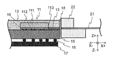
- the optical circuit device package structure 1 includes an optical circuit device 11 and a photocurable resin core (hereinafter referred to as " and a molding resin 13 covering the optical circuit device 11 and the resin core 12 .
- the optical circuit device 11 comprises a substrate 111 and a waveguide layer 112 .
- a BOX layer is also provided between the substrate 111 and the waveguide layer 112 (not shown).
- the electric element 14 may be provided.
- the direction in which light is guided in the waveguide core near the input/output end face 113 of the optical circuit device 11 is defined as the "longitudinal direction of the optical circuit core".
- the direction perpendicular to (Y direction in the figure) is the “width direction”
- the direction (Z direction) perpendicular to the horizontal plane (substrate surface) is the thickness direction.
- the “up” direction is the side to be hit, and the "down” direction is the opposite direction.
- the optical circuit device package structure 1 is formed on an electrical wiring component 15 , and the optical circuit device 11 and the electrical element 14 are mounted face down and electrically connected via electrical contacts 16 .
- a known flip-chip connection is used for Face Down mounting.
- the electrical wiring component 15 has an electrical wiring layer (not shown) and electrical connection pads for flip-chip connection on the upper surface, and multi-layer electrical wiring is formed as necessary. Also, although not shown in the drawings, another electric element 14 such as a capacitor or a coil is mounted, or a structure having a similar effect is integrally formed.
- the electrical wiring component 15 is formed with electrical wiring by through vias or inner layer wiring so as to electrically connect the upper surface and the lower surface in the thickness direction (Z direction).
- electrical contacts 16 gold bumps, copper pillars, solder balls, etc. are also formed on the lower surface facing the flip chip connection surface, and are electrically connected to the electrical mounting substrate via the electrical contacts 16 on the lower surface. ing.
- the electric mounting board is, for example, a known PCB or buildup board. Electrical contacts 16 on the bottom side are formed by solder terminals. For example, it consists of known BGA, LGA, or PGA. It should be noted that electrical contacts may be made by metal bumps (gold bumps, copper pillars, etc.) in the same manner as flip-chip connection.
- any known interposer may be used as the electrical wiring component 15, and for example, silicon, glass, ceramics (LTCC, HTCC), or a glass epoxy substrate may be used. It may also be called an interposer, subcarrier, package, or the like.
- the electrical wiring component 15 and the electrical mounting substrate may be connected by known wire bonding, if necessary, without using electrical connection via gold bumps, copper pillars, solder balls, etc. as described above.
- the electrical wiring component 15 may be composed of a thin film electrical wiring layer called a rewiring layer.
- the thin-film electrical wiring layer is, for example, a multilayer wiring layer in which copper foil layers and insulating resin layers are alternately laminated, and is manufactured by fan-out wafer level package (FOWLP) technology or fan-out panel level package (FOPLP) technology. In some cases, it is generally called a redistribution layer (RDL: Re-Distribution Layer).
- FOWLP fan-out wafer level package
- FOPLP fan-out panel level package
- RDL redistribution layer
- the electric element 14 may be any electric element such as a driver, transimpedance amplifier circuit, retimer, FPGA, ASIC, DSP, CPU/GPU, clock circuit, and the like.
- the electric element 14 is arranged on the electric wiring component 15 and mounted by flip-chip mounting.
- the mounting form of the electrical element it is not the main focus of the present invention, so it does not necessarily have to be face-down mounting, and may be face-up mounting using wire bonding or the like.
- the electrical element 14 and the optical circuit device 11 are electrically connected to electrical wiring (not shown) of the electrical wiring component 15 via respective electrical contacts 16 .
- the optical circuit device 11 is a known silicon photonics chip, the optical waveguide layer is formed on the BOX layer on the substrate, and the thickness of the waveguide substrate is, for example, 625 ⁇ m, which is the standard silicon wafer thickness. . In addition to the optical waveguide layer, it has an electric wiring layer (not shown) and has connection pads. Although not shown in the drawing, the light-emitting element, light-receiving element, modulation element, optical functional element, etc. described in the background are integrated.
- the optical circuit device 11 is integrated in a hybrid manner with an optical transmission element, an optical modulation element, and the like made of a compound semiconductor or the like, if necessary.
- a plurality of optical circuit cores are arranged in the depth direction (width direction, Y direction) of the paper surface.
- a silicon photonics chip has an optical input/output unit for inputting/outputting light to/from at least one optical input/output end surface, and a spot size converter (SSC) or the like is integrated in the optical circuit as an edge coupler.
- SSC spot size converter
- the mode field diameter of the light propagation mode in the optical circuit of silicon photonics is very small, 1 ⁇ m or less. ) is done.
- the operation when incident on the silicon photonics chip 11 is also reversible, and the present invention does not depend on the light input/output direction.
- a resin core 12 made of a photocurable resin is formed in the longitudinal direction (X direction) of the optical circuit core, in contact with the core end surface responsible for optical input/output of the optical circuit device 11 .
- the photocurable resin is a known resin that reacts to a specific wavelength and undergoes a curing reaction.
- acrylic resin, epoxy resin, silicone resin, urethane resin, oxetane resin, organic-inorganic hybrid, modified products thereof, or Substituents and the like can be used, and materials known as photoresists may be used.
- What is the curing wavelength Although it can be arbitrarily designed by adding an initiator, a dye, or the like, for example, wavelengths from ultraviolet light to visible light can be used.
- the light used for the photocurable resin is referred to as "resin curing light" 10.
- the periphery of the electrical element 14, the optical circuit device 11, and the resin core 12 is filled with the mold resin 13.
- a known mold resin 13 can be used for the package structure of a semiconductor device, etc.
- the area around the resin core 12 has a lower refractive index than the resin core 12 in the signal wavelength band and functions as a clad.
- Known acrylic resins, epoxy resins, silicone resins, urethane resins, oxetane resins, and the like can be used as the resin clad material, and halogen-substituted compounds such as fluorination may be used as appropriate to adjust the refractive index.
- the optical circuit device 11 is composed of a Si substrate 111, a BOX layer 114, and a Si waveguide ( 115 , a second waveguide core (hereinafter also referred to as “core”) 116 covering the Si waveguide 115 , and an overcladding 117 .
- the waveguide layer 112 is a Si waveguide 115 , a second waveguide core 116 and an overcladding 117 .
- the tip of the Si waveguide 115 is separated from the light input/output facet 113, that is, the Si waveguide 115 is not arranged near the light input/output facet 113, and only the second waveguide core 116 transmits light. Arranged as a waveguide layer. Here, the tip of the Si waveguide 115 may be in contact with the light input/output facet 113 .
- the resin core 12 is connected to the end surface of the second waveguide core 116 .
- a mold resin 13 is filled around the optical circuit device 11 and the resin core 12 .
- the optical circuit device 11 has a second waveguide core 116 that covers the Si waveguide 115, and the branched second waveguide core (hereinafter also referred to as "branch core").
- the resin curing light 10 is incident from an end face different from the light input/output end face 113 of 116_2 (an opposite end face in this embodiment).
- the edge coupler at the tip of the Si waveguide 115 serves as a spot size converter (SSC, arrow 118 in FIG. 3) and has a tapered shape in which the width of the thin line (waveguide) becomes narrower in the longitudinal direction (X+ direction) of the optical circuit core.
- the tapered shape of the Si waveguide 115 may be a non-linear tapered shape, a multi-step tapered shape, or an SSC structure consisting of a discontinuous body of Si core and glass material known as segmented SSC.
- a second waveguide core 116 is provided around the Si waveguide 115 .
- the signal light wavelength transits to the second waveguide core 116 after the mode field is expanded by taper or the like in the Si waveguide 115, and the substantial core at the optical input/output end face 113 of the optical circuit device 11 is , the second waveguide core 116 .
- the second waveguide core 116 is made of a material capable of propagating resin curing light, such as glass, SiON, SiN, or polymer.
- the photocurable resin core 12 is formed by gradually curing uncured resin by the resin curing light 10 emitted from the end surface of the second waveguide core 116, and is in contact with the second waveguide core 116.
- the second waveguide core 116 is branched from the Si thin wire as necessary at a location other than the SSC portion, and has a resin-cured light input portion 119 .
- the resin cured light input portion 119 of the second waveguide core 116 may be provided on the same end surface as the input/output end surface 113 in contact with the resin core 12, or may be provided on a different end surface or in the circuit.
- Resin curing light may be input by any known method, and any method such as the above-described butt connection, mirror coupling, or grating coupler via an optical fiber or the like can be applied.
- the cross section of the photocurable resin core 12 has an arbitrary shape, but is formed to have a shape similar to the mode distribution from the optical fiber core for resin curing light.
- a Gaussian beam has a shape close to a circular cross section.
- the mode shape may result in an elliptical shape.
- the photocurable resin may be used as it is as the mold material.
- the refractive index is kept lower than that of the photocurable resin core 12, and the resin is used as it is as a mold material.
- the package structure of the optical circuit device is mounted on the electrical mounting component, and the optical waveguide such as the optical fiber 21 is connected.
- the optical fibers 21 are fixed as a known optical fiber array housed with an adhesive in a fiber fixing part 22 consisting of a glass part with a V-groove and a lid part.
- the optical fiber 21 and the resin core 12 are positioned and connected. Positioning is performed with high accuracy by a known method such as active alignment or passive alignment, and fixed via an adhesive.
- optical connection is achieved by spatial coupling via a lens mechanism 23 or the like.
- the core 116 of the optical circuit device 11 and the resin core 12 are optically coupled after the resin core 12 is formed.
- the optical circuit device 11 and the optical fiber 21 are optically connected via the resin core 12 .
- the longitudinal direction By providing an optical waveguide mechanism composed of a resin core 12 extending in the X direction and a clad made of mold resin 13, an optical waveguide with an optical fiber 21 or the like and the optical circuit device 11 can be optically connected.
- the optical circuit device 11 is mounted on the electrical wiring component 15 .
- the electric element 14 may also be mounted.
- a photocurable resin is filled so as to cover the optical circuit device 11 and the electric element 14 .
- at least the periphery of the input/output end surface 113 of the optical circuit device 11 should be filled with a photocurable resin.
- the resin curing light is guided through the core 116 of the optical circuit device 11 and emitted from the input/output end surface 113 to irradiate the photocuring resin.
- the portion irradiated with the resin curing light becomes the resin core 12 .
- the molding resin 13 is filled and cured so as to cover the optical circuit device 11 and the electric element 14, including the portion where the uncured portion of the photocurable resin is removed.
- the periphery of the resin core 12 is filled with the mold resin 13 and hardened.
- the package structure of the optical circuit device according to this embodiment is manufactured.
- the electrical wiring components should be separated from the edge of the electrical wiring components by a long distance. were required to expand.
- the package structure of the optical circuit device according to the present embodiment, it is not necessary to expose the input/output end face of the optical circuit device for connection with the optical waveguide. As a result, it is no longer necessary to arrange the optical circuit device at the edge of the electrical wiring component, and the aforementioned restrictions on the package structure and the layout of the optical circuit device can be eliminated.
- the conventional configuration required precision processing such as dicing and polishing of dissimilar materials in order to expose the light input/output end faces.
- the package structure of the optical circuit device according to the present embodiment there is no need to process the optical circuit device, and the number of materials is also reduced, so the load in the process can be greatly reduced.
- the optical circuit device 11 may be face-up mounted and connected to the electrical wiring component 15 by wire bonding 24 .
- the optical circuit device 11 and the electrical element 14 may be connected by wire bonding 24 with both of them mounted face-up.
- the optical circuit device 11 and the electrical element 14 may be flip-chip connected to form a two-story flip-chip connection with the electrical wiring board.
- optical fiber 21 an example of using silicon photonics as an optical circuit device has been shown, but it is also possible to use, for example, an InP integrated circuit, quartz PLC, LN circuit, etc. in the same way. Also, any known optical fiber may be used as the optical fiber 21 . Optical fibers can also be used as other optical waveguide devices, such as polymer waveguides, as well.
- the shape of the resin core 12 may be tapered.
- the resin core 12 a beam diameter expansion or beam diameter reduction function, the beam diameter can be converted to a desired beam diameter so as to minimize the connection loss with the optical fiber, and the connection loss can be reduced.
- the resin core 12 by interposing the resin core 12 in the mold resin 13, a new optical function can be imparted.
- the resin core 12 portion may be terminated in the middle of the mold resin 13 .
- the mold resin 13 is preferably transparent to the signal light.
- the end portion of the resin core 12 may be provided with a structure that exhibits a lens function.
- the resin core part and the resin propagation part a beam diameter expansion or beam diameter reduction function in the same way, the beam diameter is converted to a desired beam diameter so as to minimize the connection loss with the optical fiber, and the connection loss is reduced. can be reduced.
- the basic components are the same as in the first embodiment, the optical circuit device 11 is a silicon photonics chip, and the electric wiring substrate is a polyimide thin film. and copper wiring.
- the difference from the first embodiment is that two types of mold resin are used, as shown in FIG.
- the first mold resin 13 exists only around the photocurable resin core 12, and is set to an appropriate value lower than the refractive index of the resin core 12 as in the first embodiment, and It functions as a cladding of
- the second mold resin 13_2 molds the optical circuit device 11 and the electric element 14 other than the first mold resin 13 portion.
- the same effect as in the first embodiment can be obtained. That is, by extending the resin core from the optical circuit device and using it as an intermediate portion for connection with the optical waveguide, it is not necessary to arrange the optical circuit device at the edge of the electrical wiring component 15, and the package structure and the optical circuit device can be improved. layout constraints can be eliminated.
- a resin different from the mold resin for general semiconductor packages is used for the mold resin around the resin core.
- the first mold resin used as the clad is used separately from the second mold resin used as a general package mold. Resin can be easily selected.
- the basic constituent elements are the same as in the first embodiment, and the electrical wiring component is the same RDL material as in the second embodiment.
- an optical function block 31 is inserted in the longitudinal direction of the photocurable resin core, as shown in FIGS. 8A and 8B.
- any block having an optical function can be applied as the optical function block 31 .
- lens components By passing through the lens, it is possible to develop a function such as reducing again the diameter of the beam that spreads during propagation through the resin core.
- any known spatial optical system bulk component such as a polarization control element, a wavelength multiplexing/demultiplexing element, and a splitter element can be used.
- an optical circuit device 11_2 is used as an optical functional block in a broad sense. Thereby, the connection between the optical circuits can also be realized through the resin core in the mold resin.
- the same effect as in the first embodiment can be obtained. That is, by extending the resin core from the optical circuit device and using it as an intermediate part for connection with the optical waveguide, it is not necessary to arrange the optical circuit device at the edge of the electrical wiring component, and the package structure and the optical circuit device can be improved. Layout constraints can be eliminated.
- the optical circuit device does not need to be subjected to the dicing and polishing processes after the molding resin is filled, and the load in the process can be greatly reduced.
- a resin different from general mold resin is used for the mold resin around the resin core.
- various optical functions and a plurality of optical circuit devices can be integrated in the resin core waveguide on the electrical wiring component, effectively utilizing the space inside the package without degrading the optical characteristics. Functionality can be imparted.
- the difference from the first to third embodiments is that the longitudinal direction of the resin core differs from the longitudinal direction (X direction) of the optical circuit (optical waveguide) core, as shown in FIGS. 9A and 9B.
- the resin core 12 is formed upward at a predetermined angle with respect to the longitudinal direction (X direction) of the optical circuit (optical waveguide) core.
- This configuration can be formed by inclining the input/output end surface 113 of the optical circuit device 11 in advance, as shown in FIG. 9A.
- the resin curing light enters the optical circuit device 11 at an angle determined by Snell's law. It is emitted from the output end face 113 . Since the photocurable resin core 12 is formed along the resin curing light, it is formed at a predetermined angle with respect to the longitudinal direction (X direction) of the optical circuit (optical waveguide) core.
- the end face of the mold resin 13 on the side connected to the optical component such as the optical fiber 21 may be inclined with respect to the thickness direction (Z direction) of the wiring component.
- the optical fiber array can also be connected in accordance with the angle of the end surface of the mold resin 13 . The combination of these angles is appropriately determined by design, and the end surface of the mold resin 13 may remain in the thickness direction (Z direction) of the wiring component without being inclined.
- the same effect as in the first embodiment can be obtained. That is, by extending the resin core from the optical circuit device and using it as an intermediate part for connection with the optical waveguide, it is not necessary to arrange the optical circuit device at the edge of the electrical wiring component, and the package structure and the optical circuit device can be improved. Layout constraints can be eliminated.
- the optical axis can be offset with respect to the thickness direction (Z direction) of the electrical wiring component.
- the position of the end of the resin core 12 at the end of the mold resin on the side connected to the optical component such as the optical fiber can be separated upward (raised) from the electrical wiring component.
- the fiber fixing parts and the like are large, and when the package is mounted on the electrical mounting board, mechanical interference may occur between the electrical mounting board and the fiber fixing parts.
- an optical path conversion component 41 that is, a mirror is arranged as an optical function block in the third embodiment, and a photocurable resin
- the position of the end of the core 12_2 is the upper surface of the package structure (mold resin 13) of the optical circuit device 11.
- the end of the photocurable resin core is provided on the mold resin end surface perpendicular to the core longitudinal direction (X direction) of the optical circuit.
- the end of the photocurable resin core 12_2 is provided on the surface (eg, upper surface) of the mold resin 13 parallel to the longitudinal direction (X direction) of the optical circuit core.
- the resin cores are composed of a first resin core 12_1 whose longitudinal direction is the core longitudinal direction of the optical circuit (light waveguiding direction of the optical circuit device, X direction), and a thickness direction (Z direction) whose longitudinal direction is the first resin core 12_1. and a second resin core 12_2 in the same direction, and an optical path conversion component 41 is mounted between the first resin core 12_1 and the second resin core 12_2.
- the second resin core end surface 12_2 connected to the optical component (for example, the optical fiber 21) is arranged on the upper surface of the mold resin 13.
- a micromirror is preferable as the mirror, and it is preferable that it has sufficient reflectance for both the signal wavelength and the resin curing light.
- the same effect as in the first embodiment can be obtained. That is, by extending the resin core from the optical circuit device and using it as an intermediate part for connection with the optical waveguide, it is not necessary to arrange the optical circuit device at the edge of the electrical wiring component, and the package structure and the optical circuit device can be improved. Layout constraints can be eliminated.
- the output end surface of the resin core is arranged on the upper surface of the mold resin.
- the fiber fixing parts are large, and when the package is mounted on the electrical mounting board, mechanical interference may occur between the electrical mounting board and the fiber fixing parts.
- the fiber fixing component 22 and the electrical mounting board can be mounted without coming into contact with each other.
- the package structure of the optical circuit device is manufactured at the wafer level, light can be input and output from the upper surface of the wafer, so it has excellent testability and can be easily inspected.
- the package structure of the optical circuit device has the end of the resin core 12_2 on the upper surface (the surface facing the electrical wiring component 15) of the package structure (mold resin 13), and the optical fiber 21 may be connected to an optical waveguide.
- the mold resin on the upper surface of the package is removed by polishing or grinding.
- the thickness of the mold resin 41 can be reduced, the resin core 12_2 can be shortened.
- another optical path conversion component 41_2 may be provided on the side of the fiber fixing component 22 so that the longitudinal direction of the optical fiber 21 and the longitudinal direction of the optical circuit core (X direction) are substantially parallel. good.
- FIG. 1 an example in which one molding resin is applied is shown.
- FIG. 1 A structure can be used in which the periphery is filled with the first mold resin 13 that functions as a clad for the resin core, and the other portion is filled with the second mold resin 13_2.
- the present invention relates to a package structure of an optical circuit device, and can be applied to equipment and systems such as optical communication.
Landscapes
- Physics & Mathematics (AREA)
- Engineering & Computer Science (AREA)
- Microelectronics & Electronic Packaging (AREA)
- General Physics & Mathematics (AREA)
- Optics & Photonics (AREA)
- Optical Integrated Circuits (AREA)
- Optical Couplings Of Light Guides (AREA)
Abstract
Description
本発明は、光回路デバイスと光部品とを接続する光回路デバイスのパッケージ構造およびその製造方法に関する。 The present invention relates to a package structure of an optical circuit device that connects an optical circuit device and an optical component, and a manufacturing method thereof.
近年のインターネットトラフィックの急増に対応すべく、データセンタネットワークの通信容量の拡大が求められる。伝送容量のさらなる拡大および低消費電力化に対応すべく短中距離用途においても光で伝送する光インタコネクションの導入が進んでいる。 In order to respond to the rapid increase in Internet traffic in recent years, it is necessary to expand the communication capacity of the data center network. In order to cope with further expansion of transmission capacity and reduction of power consumption, the introduction of optical interconnection for transmission by light is progressing even for short and medium distance applications.
光インタコネクションの代表的な方式においては、プリント基板上に配置されたレーザダイオード(LD)などの光発光素子とフォトダイオード(PD)などの光受光素子間を光導波路や光ファイバなどの光伝送媒体を用いて伝送することで信号処理が実現されている。 In a typical optical interconnection system, optical transmission such as an optical waveguide or an optical fiber is performed between a light emitting element such as a laser diode (LD) and a light receiving element such as a photodiode (PD) arranged on a printed circuit board. Signal processing is realized by transmission using a medium.
伝送方式によっては、光発光素子には、光変調素子などが集積されるか、あるいはディスクリートに接続され、さらに電気-光変換を行うドライバなどが接続される。これら光発光素子、光変調素子、ドライバなどを含む構成が光送信機としてプリント基板(PCB:Printed circuit board)などの電気実装基板上に搭載されている。 Depending on the transmission method, the optical light emitting element is integrated with an optical modulation element or the like, or connected discretely, and further connected to a driver or the like that performs electrical-to-optical conversion. A configuration including these light emitting elements, light modulating elements, drivers, etc. is mounted as an optical transmitter on an electrical mounting board such as a printed circuit board (PCB).
同様に、光受光素子には、光処理機などが適宜集積されるか、あるいはディスクリートに接続され、さらに光-電気変換を行う電気増幅回路などが接続される。これら光受光素子、光処理機、電気増幅回路などを含む構成が光受信機としてプリント基板上に実装されている。これら光送信機と光受信機とを一体化した光送受信機などがパッケージ内やプリント基板上に搭載され、光ファイバなどの光伝送媒体と光学的に接続されることで、光インタコネクションが実現されている。また、トポロジーによっては、光スイッチなどの中継器などを介して実現されている。 Similarly, the light-receiving element is appropriately integrated with an optical processor or the like, or connected discretely, and further connected with an electric amplifier circuit for performing optical-electrical conversion. A configuration including these light receiving element, optical processor, electric amplifier circuit, etc. is mounted on a printed circuit board as an optical receiver. Optical interconnection is achieved by mounting an optical transceiver, which integrates an optical transmitter and an optical receiver, in a package or on a printed circuit board and optically connecting it to an optical transmission medium such as an optical fiber. It is Also, depending on the topology, it is realized through a repeater such as an optical switch.
前記光発光素子や光受光素子、光変調素子としては、シリコンやゲルマニウムなどの半導体や、インジウムリン(InP)やガリウムヒ素(GaAs)、インジウムガリウムヒ素(InGaAs)等に代表されるIII-V族半導体などの材料を用いる素子が実用化されている。近年では、これらの素子と共に、光の伝播機構を有するシリコン光回路(シリコンフォトニクス)やインジウムリン光回路などを集積した光導波路型の光送受信機が発展している。また光変調素子としては、半導体の他に、ニオブ酸リチウムなどの強誘電体系やポリマーなどの材料を用いる場合もある。 As the light emitting device, the light receiving device, and the light modulation device, semiconductors such as silicon and germanium, III-V group represented by indium phosphide (InP), gallium arsenide (GaAs), indium gallium arsenide (InGaAs), etc. Devices using materials such as semiconductors have been put to practical use. In recent years, along with these elements, optical waveguide type optical transceivers have been developed in which a silicon optical circuit (silicon photonics) having a light propagation mechanism, an indium phosphorous optical circuit, or the like are integrated. In addition to semiconductors, materials such as ferroelectrics such as lithium niobate and polymers may also be used as light modulation elements.
更に、上記の光発光素子や光受光素子、光変調素子と共に、石英ガラスなどからなる平面光波回路(Planar Lightwave Circuit)などからなる光機能素子が集積されることがある。光機能素子としてはスプリッタ、波長合分波器、光スイッチ、偏波制御素子、光フィルタなどがある。以降、上記の光の伝播、導波機構を有する光発光素子、光受光素子、光変調素子、光機能素子、光増幅素子などを集積したデバイスを光導波路デバイスと呼ぶこととする。光導波路デバイスの中でもシリコンフォトニクスを用いた光導波路デバイスは集積性、量産性、電気部品との親和性に優れ、次世代の光インタコネクションを実現する上でのキーデバイスとして着目されている。 Furthermore, optical functional elements such as planar lightwave circuits made of silica glass are sometimes integrated together with the above light emitting elements, light receiving elements, and light modulating elements. Optical functional devices include splitters, wavelength multiplexers/demultiplexers, optical switches, polarization control devices, optical filters, and the like. Hereinafter, a device in which a light emitting device, a light receiving device, an optical modulation device, an optical functional device, a light amplifying device, etc. having the above light propagation and waveguiding mechanisms are integrated will be referred to as an optical waveguide device. Among optical waveguide devices, optical waveguide devices using silicon photonics excel in integration, mass production, and compatibility with electrical components, and are attracting attention as key devices in realizing next-generation optical interconnection.
光回路デバイスと光ファイバをはじめとする光導波路とを接続する代表的な方法の一つは、光回路の光入出力を担う1以上の端面に対して、光回路と光導波路とを突き合わせて接続する構造である。例えば、光導波路の一つである光ファイバを、V溝を形成したガラスなどと一体化された光ファイバアレイとし、このアレイ構造における光ファイバの各コアと光回路デバイスの各コアとを位置決めして接続される。このとき、接続損失を最小化するためには、サブミクロン単位で光回路デバイスの各コアと光ファイバの各コアとを位置決め(以下、調心と呼ぶ)・固定することが必要である。この位置決めでは、光を入出力させてパワーのモニタと同時に調心(光学調心)し、接着剤などを充填させて固定する(非特許文献1)。 One of the representative methods for connecting an optical circuit device and an optical waveguide such as an optical fiber is to butt the optical circuit and the optical waveguide against one or more end faces that are responsible for the optical input/output of the optical circuit. It is a structure to connect. For example, an optical fiber array, which is one of the optical waveguides, is integrated with glass or the like in which a V-groove is formed, and each core of the optical fiber and each core of the optical circuit device in this array structure are positioned. connected. At this time, in order to minimize the connection loss, it is necessary to position (hereinafter referred to as alignment) and fix each core of the optical circuit device and each core of the optical fiber in submicron units. In this positioning, light is input and output, alignment is performed simultaneously with power monitoring (optical alignment), and adhesive or the like is filled and fixed (Non-Patent Document 1).
しかしながら、光回路デバイスと光導波路の突合せ接続においては、光回路と光導波路の入出力端面を各々面一として、平行になるように突き合わせる必要があった。ここで、端面を面一にするために、入出力端面をダイシングまたは研磨する必要があり、製造工程上の負荷を増加させていた。 However, in the butt connection of the optical circuit device and the optical waveguide, it was necessary to align the input and output end faces of the optical circuit and the optical waveguide so that they were parallel to each other. Here, in order to make the end faces flush, it was necessary to dicing or polish the input and output end faces, which increased the load on the manufacturing process.
また、公知の半導体デバイスのパッケージ構造6では、図13Aに示すように、電気配線部品65上に電気素子64が搭載され、全体が樹脂63でモールドされる。電気配線部品65は、例えばセラミックと金属配線層からなる電気配線部品である。電気接点用のパッドや多層電気配線部などは省略している。電気配線部品65上には、電気素子64が搭載されており、電気配線部品の電気配線を介して電気的に接続されている。光回路デバイス61は、各種光回路デバイスであり、電気配線部品上に搭載され、モールド樹脂63に覆われている。
Also, in the known semiconductor
このパッケージ構造において、図13Bに示すように、突合せ接続をはじめとする光接続させ、光回路デバイスの実装構造を実現するためには、光回路デバイス61の入出力端面68は、モールド樹脂63から接続端面を露出させる必要がある。そこで、光回路デバイス61を電気配線部品65のエッジ周辺に配置する必要があり、パッケージ構造や光回路デバイス61のレイアウトを制約する要因となっていた。また、モールド樹脂63や電気配線部品65とともに光回路デバイス61をダイシングまたは研磨する工程が必要であり、多くの異種材料で工程を一括で精密に行うことは負担が大きかった。
In this package structure, as shown in FIG. It is necessary to expose the connection end face. Therefore, it is necessary to arrange the
上述したような課題を解決するために、本発明に係る光回路デバイスのパッケージ構造は、光部品と接続される光回路デバイスのパッケージ構造であって、電気配線部品上に、コアとクラッドとを有する光回路デバイスと、光硬化性樹脂に光照射して硬化され、前記前記コアの端面に配置される樹脂コアと、前記光回路デバイスと、前記樹脂コアとを覆うモールド樹脂とを備え、少なくとも前記樹脂コアの周囲のモールド樹脂の屈折率が、前記樹脂コア層の屈折率よりも低いことを特徴とする。 In order to solve the above-described problems, an optical circuit device package structure according to the present invention is a package structure for an optical circuit device connected to an optical component, wherein a core and a clad are formed on an electrical wiring component. a resin core cured by irradiating a photocurable resin with light and arranged on an end surface of the core; and a mold resin covering the optical circuit device and the resin core, and at least The refractive index of the mold resin surrounding the resin core is lower than the refractive index of the resin core layer.
また、本発明に係る光回路デバイスのパッケージ構造の製造方法は、電気配線部品上に光回路デバイスを配置する工程と、少なくとも前記光回路デバイスの入出力端面の周囲に光硬化樹脂を充填する工程と、前記光回路デバイスのコアに樹脂硬化光を導波させ、前記入出力端面から出射し、前記光硬化樹脂に照射し、樹脂コアを形成する工程と、前記光硬化樹脂の未硬化部分を除去する工程と、少なくとも樹脂コアの周囲にモールド樹脂を充填し、硬化する工程とを備える。 A method of manufacturing a package structure for an optical circuit device according to the present invention includes the steps of placing the optical circuit device on an electrical wiring component, and filling at least the periphery of the input/output end faces of the optical circuit device with a photocurable resin. a step of guiding resin curing light through the core of the optical circuit device, emitting the light from the input/output end surface, and irradiating the photocurable resin to form a resin core; and a step of filling mold resin around at least the resin core and curing the mold resin.
本発明によれば、レイアウトの自由度が高く、簡易に製造できる光回路デバイスのパッケージ構造を提供できる。 According to the present invention, it is possible to provide a package structure for an optical circuit device that has a high degree of freedom in layout and can be manufactured easily.
<第1の実施の形態>
本発明の第1の実施の形態に係る光回路デバイスのパッケージ構造について、図1~図6Cを参照して説明する。
<First Embodiment>
A package structure of an optical circuit device according to a first embodiment of the present invention will be described with reference to FIGS. 1 to 6C.
<光回路デバイスのパッケージ構造の構成>
本実施の形態に係る光回路デバイスのパッケージ構造1は、図1に示すように、光回路デバイス11と、光回路デバイス11の光入出力端面113に接続する光硬化性樹脂コア(以下、「樹脂コア」という。)12と、光回路デバイス11と樹脂コア12とを覆うモールド樹脂13とを備える。ここで、光回路デバイス11は、基板111と導波路層112とを備える。また、基板111と導波路層112との間にBOX層を備える(図示せず)。
<Configuration of Package Structure of Optical Circuit Device>
As shown in FIG. 1, the optical circuit
また、電気素子14を備えてもよい。
Also, the
以下、水平面(基板表面)において、光回路デバイス11の入出射端面113近傍の導波路コアで光が導波する方向(図中、X方向)を「光回路コアの長手方向」とし、長手方向に垂直な方向(図中、Y方向)を「幅方向」、水平面(基板表面)に垂直な方向(Z方向)を厚さ方向とし、電気配線部品15に対して、光回路デバイス11が配置される側を「上」方向とし、その逆方向を「下」方向とする。
Hereinafter, in the horizontal plane (substrate surface), the direction in which light is guided in the waveguide core near the input/
光回路デバイスのパッケージ構造1は、一例として、電気配線部品15上に形成され、光回路デバイス11と電気素子14がFace Downで実装され、電気接点16を介して電気的に接続されている。Face Down実装としては公知のフリップチップ接続が用いられている。
As an example, the optical circuit
電気配線部品15は、電気配線層(図示せず)およびフリップチップ接続用の電気接続パッドを上面に有しており、必要に応じて電気の多層配線が形成されている。また、図面上では省略するが、キャパシタやコイルなど別の電気素子14が搭載、または同様の効果を有する構造が一体で形成されている。
The
電気配線部品15は、厚さ方向(Z方向)に向かって上面と下面を電気接続するように貫通ビアあるいは内層配線による電気配線が形成されている。また、フリップチップ接続面とは正対する下面においても同様に電気接点16(金バンプ、銅ピラー、はんだボールなど)が形成され、下面の電気接点16を介して電気実装基板と電気的に接続されている。
The
電気実装基板は、例えば公知のPCBやビルドアップ基板である。下面側の電気接点16ははんだ端子により形成される。例えば公知のBGAまたはLGA、PGAからなる。なお、フリップチップ接続と同様に金属バンプ(金バンプ、銅ピラーなど)による電気接点としてもよい。
The electric mounting board is, for example, a known PCB or buildup board.
電気配線部品15としては、公知のインタポーザであれば任意であり、例えばシリコン、ガラス、セラミック(LTCC、HTCC)やガラエポ基板などいずれでもよい。またインタポーザやサブキャリア、パッケージなどと呼んでもよい。
Any known interposer may be used as the
電気配線部品15と電気実装基板には、必要に応じて前述のような金バンプ、銅ピラー、はんだボールなどを介した電気接続を用いずに、公知のワイヤボンディングにより接続してもよい。また電気配線部品15として、再配線層とよばれる薄膜電気配線層から構成してもよい。
The
薄膜電気配線層は、例えば銅箔層と絶縁樹脂層が交互に積層された多層配線層であり、ファンアウトウェハレベルパッケージ(FOWLP)技術、もしくはファンアウトパネルレベルパッケージ(FOPLP)技術によって製造される場合には一般的に再配線層(RDL:Re-Distribution Layer)と呼ばれている。 The thin-film electrical wiring layer is, for example, a multilayer wiring layer in which copper foil layers and insulating resin layers are alternately laminated, and is manufactured by fan-out wafer level package (FOWLP) technology or fan-out panel level package (FOPLP) technology. In some cases, it is generally called a redistribution layer (RDL: Re-Distribution Layer).
電気素子14は、例えばドライバやトランスインピーダンス増幅回路、リタイマ、FPGA、ASIC、DSP、CPU/GPU、クロック回路、など任意の電気素子でよい。電気素子14は、電気配線部品15上に配置されフリップチップ実装により実装されている。なお、電気素子の実装形態に関しては、本発明の主眼でないため必ずしもFace Down実装でなくてもよく、例えばワイヤボンディングなどを用いてFace Upの実装としてもよい。電気素子14と光回路デバイス11とは電気配線部品15の電気配線(図示せず)とそれぞれの電気接点16を介して電気的に接続されている。
The
光回路デバイス11は、公知のシリコンフォトニクスチップであり、光導波路層は基板上のBOX層上に形成されており、導波路基板の厚さは例えば標準的なシリコンウェハ厚さである625μmである。また光導波路層以外にも電気配線層(図示せず)を有しており、接続用のパッドを有している。図面上では省略するが背景で述べたような発光素子、受光素子、変調素子、光機能素子などが集積されている。
The
また、光回路デバイス11は、必要に応じて化合物半導体などからなる光送信素子や光変調素子などとハイブリッドに一体化されている。光回路デバイス11において、複数の光回路コアが紙面奥行き方向(幅方向、Y方向)に配置されている。
In addition, the
シリコンフォトニクスチップは、少なくとも1つの光入出力端面において外部へ光を入出力する光入出力部を備えており、エッジカップラーとしてスポットサイズ変換器(SSC)などが光回路内に集積されている。一般に、シリコンフォトニクスの光回路内での光伝搬モードのモードフィールド径は1μm以下と非常に小さいが、エッジカップラーにより3μmから10μm程度までそのモードフィールド径が拡大された状態で光ビームは出射(入射)される。 A silicon photonics chip has an optical input/output unit for inputting/outputting light to/from at least one optical input/output end surface, and a spot size converter (SSC) or the like is integrated in the optical circuit as an edge coupler. In general, the mode field diameter of the light propagation mode in the optical circuit of silicon photonics is very small, 1 μm or less. ) is done.
以下、シリコンフォトニクスチップ11からの光出射を例に説明するが、シリコンフォトニクスチップ11に入射する場合の動作についても可逆的に動作し、本発明は当然光の入出力方向に依らない。
Although the light emitted from the
図1に示すように、光回路デバイス11の光入出力を担うコア端面と接して、光硬化性樹脂からなる樹脂コア12が光回路コアの長手方向(X方向)に形成されている。
As shown in FIG. 1, a
光硬化性樹脂は、特定の波長に対して反応し硬化反応が進む公知の樹脂であり、例えばアクリル樹脂、エポキシ樹脂、シリコーン樹脂、ウレタン樹脂、オキセタン樹脂、有機無機ハイブリッドや、それらの変性体や置換体などを用いることができ、フォトレジストとして知られる材料を用いてもよい。硬化波長は。開始材や色素などの添加により任意に設計できるが、例えば紫外光から可視光程度の波長を用いることができる。ここで、光硬化性樹脂に用いる光を「樹脂硬化光」10という。 The photocurable resin is a known resin that reacts to a specific wavelength and undergoes a curing reaction. For example, acrylic resin, epoxy resin, silicone resin, urethane resin, oxetane resin, organic-inorganic hybrid, modified products thereof, or Substituents and the like can be used, and materials known as photoresists may be used. What is the curing wavelength? Although it can be arbitrarily designed by adding an initiator, a dye, or the like, for example, wavelengths from ultraviolet light to visible light can be used. Here, the light used for the photocurable resin is referred to as "resin curing light" 10. FIG.
また、図1に示すように、電気配線部品15上において、電気素子14、光回路デバイス11、樹脂コア12の周囲にはモールド樹脂13が充填されている。
Further, as shown in FIG. 1, on the
モールド樹脂13は、半導体デバイスのパッケージ構造などで公知のモールド樹脂13を用いることができ、樹脂コア12の周囲においては樹脂コア12よりも信号波長帯において屈折率が低く、クラッドとして機能している。樹脂クラッド材として、公知のアクリル樹脂、エポキシ樹脂、シリコーン樹脂、ウレタン樹脂、オキセタン樹脂などを用いることができ、屈折率を調整するために適宜フッ素化などのハロゲン置換体を用いてもよい。
As the
光回路デバイス11のパッケージ構造の光入出力端面113領域で、光回路デバイス11は、図2の拡大概略側面図に示すように、順に、Si基板111と、BOX層114と、Si導波路(以下、「他のコア」ともいう。)115と、Si導波路115を覆う第2導波路コア(以下、「コア」ともいう。)116と、オーバクラッド117を備える。ここで、導波路層112は、Si導波路115と、第2導波路コア116と、オーバクラッド117である。
In the optical input/
また、Si導波路115の先端は、光入出力端面113と離間しており、すなわち、光入出力端面113近傍では、Si導波路115は配置されず、第2導波路コア116のみが光の導波層として配置される。ここで、Si導波路115の先端が光入出力端面113と接する構成であってもよい。
The tip of the
第2導波路コア116の端面に、樹脂コア12が接続される。
The
光回路デバイス11と樹脂コア12との周囲に、モールド樹脂13が充填される。
A
また、光回路デバイス11は、図3に示すように、Si導波路115を覆う第2導波路コア116が分岐され、分岐された第2導波路コア(以下、「分岐コア」ともいう。)116_2の光入出力端面113と異なる端面(本実施の形態では反対側の端面)より樹脂硬化光10が入射される。
In addition, as shown in FIG. 3, the
Si導波路115の先端のエッジカプラーは、スポットサイズ変換器(SSC、図3中矢印118)として、光回路コアの長手方向(X+方向)に細線(導波路)幅が細くなるテーパ形状を有する。Si導波路115のテーパ形状には、非線形テーパ形状や多段のテーパ形状、またはセグメンテッドSSCとして知られるようなSiコアとガラス材料の非連続体からなるSSC構造を用いてもよい。
The edge coupler at the tip of the
また、SSCにおいて、Si導波路115の周囲には第2導波路コア116が設けられている。信号光波長は、Si導波路115において、テーパなどでモードフィールドが拡大された後に第2導波路コア116に遷移しており、光回路デバイス11の光入出力端面113での実質的なコアは、第2導波路コア116が担っている。このとき、第2導波路コア116は、樹脂硬化光を伝搬することが可能な材料からなり、例えばガラス、SiON、SiN、ポリマーなどで構成される。
Also, in the SSC, a
光硬化性樹脂コア12は、第2導波路コア116端面から出射される樹脂硬化光10により未硬化の樹脂が次第に硬化することで形成されており、第2導波路コア116と接している。
The
図3に示すように、第2導波路コア116は、SSC部以外の個所において必要に応じてSi細線と分岐され、樹脂硬化光入力部119を備えている。第2導波路コア116の樹脂硬化光入力部119は、樹脂コア12と接する入出力端面113と同一の端面に設けてもよいし、異なる端面や回路内に設けてもよい。樹脂硬化光は、公知のいずれの方法で入力すればよく、例えば光ファイバ等を介した前述の突合せ接続やミラー結合、グレーティングカプラなど任意の方法が適用できる。
As shown in FIG. 3, the
このとき、光硬化性樹脂コア12の断面は任意の形状であるが、樹脂硬化光用の光ファイバコアからのモード分布に類似した形状として形成される。例えば、ガウシアンビームであれば、円形断面に近い形状になる。実際は、モード形状によって楕円形状になってもよい。周囲を覆うモールド樹脂13を充填する前に、光硬化性樹脂の未硬化分は除去され、異なる材料が充填されている。
At this time, the cross section of the
なお、樹脂特性によっては光硬化性樹脂をモールド材料としてそのまま用いてもよい。例えば、硬化波長や硬化のメカニズム、共重合物の添加などによって、硬化後の樹脂屈折率が異なる樹脂を用いることで、光硬化性樹脂コア12よりも屈折率を低く保ち、モールド材料としてそのまま用いることもできる。
Depending on the resin characteristics, the photocurable resin may be used as it is as the mold material. For example, by using a resin with a different resin refractive index after curing depending on the curing wavelength, curing mechanism, addition of a copolymer, etc., the refractive index is kept lower than that of the
本実施の形態に係る光回路デバイスの実装構造では、図4A~Cに例として示すように、光回路デバイスのパッケージ構造が、電気実装部品に搭載され、光ファイバ21等の光導波路が接続される。光ファイバ21はV溝を形成したガラス部品と、リッド部品とからなるファイバ固定部品22の中に接着剤で収容された公知の光ファイバアレイとして固定されている。
In the mounting structure of the optical circuit device according to the present embodiment, as shown in FIGS. 4A to 4C as an example, the package structure of the optical circuit device is mounted on the electrical mounting component, and the optical waveguide such as the
図4Aに示す構成例では、光ファイバ21と樹脂コア12が位置決めされ、接続されている。位置決めは、アクティブアライメントやパッシブアライメントなど公知の方法で高精度に実施されており、接着剤を介して固定されている。
In the configuration example shown in FIG. 4A, the
図4B、Cに示す構成例では、レンズ機構23などを介して空間結合により光接続がなされている。このとき、光回路デバイス11のコア116と樹脂コア12は、樹脂コア12の形成後に光学的に結合されている。さらに、樹脂コア12と光ファイバ21が光接続されることで、樹脂コア12を介した光回路デバイス11と光ファイバ21との光接続がなされている。
In the configuration examples shown in FIGS. 4B and 4C, optical connection is achieved by spatial coupling via a
以上のように、電気配線部品上に搭載された光回路デバイス11の周囲にモールド樹脂13が充填されたパッケージ構造において、光回路デバイス11の入出力端面113と接して光回路コアの長手方向(X方向)に延在する樹脂コア12とモールド樹脂13のクラッドから構成される光導波機構を備えることにより、光ファイバ21等との光導波路と光回路デバイス11を光接続できる。
As described above, in the package structure in which the
<光回路デバイスのパッケージ構造の製造方法>
以下に、光回路デバイスのパッケージ構造の製造方法の一例を説明する。
<Manufacturing Method for Package Structure of Optical Circuit Device>
An example of the manufacturing method of the package structure of the optical circuit device will be described below.
初めに、電気配線部品15上に光回路デバイス11を搭載する。また、電気素子14も搭載してもよい。
First, the
次に、光回路デバイス11と電気素子14を覆うように光硬化樹脂を充填する。ここで、少なくとも前記光回路デバイス11の入出力端面113の周囲に光硬化樹脂を充填すればよい。
Next, a photocurable resin is filled so as to cover the
次に、光回路デバイス11のコア116に樹脂硬化光を導波させ、前記入出力端面113から出射し、光硬化樹脂に照射する。その結果、光硬化樹脂において、樹脂硬化光に照射された部分が樹脂コア12となる。
Next, the resin curing light is guided through the
次に、光硬化樹脂の未硬化部分を除去する。 Next, the uncured portion of the photocurable resin is removed.
最後に、光硬化樹脂の未硬化部分を除去した部分を含めて、光回路デバイス11と電気素子14を覆うように、モールド樹脂13を充填し、硬化する。ここで、少なくとも樹脂コア12の周囲にモールド樹脂13を充填し、硬化すればよい。
Finally, the
このように、本実施の形態に係る光回路デバイスのパッケージ構造が製造される。 Thus, the package structure of the optical circuit device according to this embodiment is manufactured.
<効果>
以下に、本実施の形態に係る光回路デバイスのパッケージ構造の効果を説明する。
<effect>
The effect of the package structure of the optical circuit device according to this embodiment will be described below.
従来のモールド樹脂を充填した光回路のパッケージ構造においては、光回路デバイスと光ファイバ等の外部の光導波路と低損失に光接続するために、光回路の入出力端面を露出させるダイシングや研磨などの工程を必要とした。その結果、光回路を電気配線部品のエッジ近傍に配置することが必要となり、パッケージ構造や光回路デバイスのレイアウトに制約が生じていた。 In the conventional package structure of an optical circuit filled with mold resin, dicing and polishing are used to expose the input/output end face of the optical circuit in order to optically connect the optical circuit device to an external optical waveguide such as an optical fiber with low loss. required the process of As a result, it has become necessary to arrange the optical circuit near the edge of the electrical wiring component, which has imposed restrictions on the package structure and the layout of the optical circuit device.
例えば、光回路上の電気接点をパッケージに接続し、その電気配線部品で配線を展開して電気実装基板との電気接点と接続するためには、電気配線部品のエッジから長い距離で離間させて展開することが要求されていた。 For example, in order to connect the electrical contacts on the optical circuit to the package, develop the wiring with the electrical wiring components, and connect the electrical contacts to the electrical mounting board, the electrical wiring components should be separated from the edge of the electrical wiring components by a long distance. were required to expand.
その結果、光回路レイアウト上での電気接点位置を調整したり、電気配線部品での電気配線のためのレイアウトを工夫したりことが求められ、結果として全体のサイズを増加させてしまう欠点があった。 As a result, it is necessary to adjust the position of the electrical contacts on the optical circuit layout and devise a layout for the electrical wiring in the electrical wiring parts, resulting in an increase in the overall size. rice field.
一方、本実施の形態に係る光回路デバイスのパッケージ構造によれば、光導波路との接続のために、光回路デバイスの入出力端面を露出させる必要がなくなる。その結果、光回路デバイスを電気配線部品のエッジに配置する必要がなくなり、前述のパッケージ構造や光回路デバイスのレイアウト制約を排除することができる。 On the other hand, according to the package structure of the optical circuit device according to the present embodiment, it is not necessary to expose the input/output end face of the optical circuit device for connection with the optical waveguide. As a result, it is no longer necessary to arrange the optical circuit device at the edge of the electrical wiring component, and the aforementioned restrictions on the package structure and the layout of the optical circuit device can be eliminated.
また、従来の構成では、光入出力端面の露出のために異種材料のダイシングや研磨などの精密加工を必要とした。 In addition, the conventional configuration required precision processing such as dicing and polishing of dissimilar materials in order to expose the light input/output end faces.
一方、本実施の形態に係る光回路デバイスのパッケージ構造によれば、加工を光回路デバイスに対して行う必要がなくなり、材料数も低減することから工程上の負荷を大きく低減できる。 On the other hand, according to the package structure of the optical circuit device according to the present embodiment, there is no need to process the optical circuit device, and the number of materials is also reduced, so the load in the process can be greatly reduced.
本実施の形態では、電気素子および光回路デバイスがともにFace down実装される例を示したが、電気素子と光回路デバイスのいずれかまたは双方をFace up実装としてもよい。 In this embodiment, an example in which both the electrical element and the optical circuit device are facedown mounted has been shown, but either or both of the electrical element and the optical circuit device may be faceup mounted.
例えば、図5Aに示すように、光回路デバイス11をFace up実装として、電気配線部品15とワイヤボンディング24で接続してもよい。または、図5Bに示すように、双方をFace up実装としてワイヤボンディング24で光回路デバイス11と電気素子14とを接続してもよい。また、図示しないが、光回路デバイス11と電気素子14とをフリップチップで接続して電気配線基板と2階建てのフリップチップ接続としてもよい。
For example, as shown in FIG. 5A, the
本実施の形態では、光回路デバイスとしてシリコンフォトニクスを用いる例を示したが、例えばInP集積回路や石英PLC、LN回路などを用いても同様に適用できる。また、光ファイバ21として公知のいずれの光ファイバを用いてもよい。また、光ファイバを別の光導波路デバイス、例えばポリマー導波路としても同様に用いることができる。
In the present embodiment, an example of using silicon photonics as an optical circuit device has been shown, but it is also possible to use, for example, an InP integrated circuit, quartz PLC, LN circuit, etc. in the same way. Also, any known optical fiber may be used as the
また、図6A、Bに示すように、樹脂コア12の形状はテーパ形状として形成してもよい。これにより、樹脂コア12部にビーム径拡大あるいはビーム径縮小機能を付与することで、光ファイバとの接続損失を最小化するように所望のビーム径に変換して接続損失を低減することができる。換言すると、モールド樹脂13において樹脂コア12を介することで、新たな光学機能を付与することができる。
Also, as shown in FIGS. 6A and 6B, the shape of the
また、図6Cに示すように、樹脂コア12部をモールド樹脂13の途中で終端させてもよい。この場合、信号光はモールド樹脂13の中を伝搬するため、信号光に対してモールド樹脂13は透明であることが好ましい。また、樹脂コア12の終端部にレンズ機能を発現する構造を付与してもよい。
Also, as shown in FIG. 6C, the
これにより、同様に樹脂コア部および樹脂伝搬部にビーム径拡大あるいはビーム径縮小機能を付与することで、光ファイバとの接続損失を最小化するように所望のビーム径に変換して接続損失を低減することができる。 As a result, by giving the resin core part and the resin propagation part a beam diameter expansion or beam diameter reduction function in the same way, the beam diameter is converted to a desired beam diameter so as to minimize the connection loss with the optical fiber, and the connection loss is reduced. can be reduced.
<第2の実施の形態>
本発明の第2の実施の形態に係る光回路デバイスのパッケージ構造について、図7を参照して説明する。
<Second Embodiment>
A package structure of an optical circuit device according to a second embodiment of the present invention will be described with reference to FIG.
<光回路デバイスのパッケージ構造の構成>
本実施の形態に係る光回路デバイスのパッケージ構造2において、基本的な構成要素は、第1の実施の形態と同様であり、光回路デバイス11はシリコンフォトニクスチップであり、電気配線基板はポリイミド薄膜と銅配線からなるRDL基板である。
<Configuration of Package Structure of Optical Circuit Device>
In the optical circuit
第1の実施の形態との差異は、図7に示すように、2種類のモールド樹脂を用いている点がある。第1のモールド樹脂13は光硬化性樹脂コア12の周囲にのみ存在し、第1の実施の形態と同様に、樹脂コア12の屈折率よりも低い適切な値に設定され、樹脂コア伝搬部のクラッドとして機能している。
The difference from the first embodiment is that two types of mold resin are used, as shown in FIG. The
一方、第2のモールド樹脂13_2は、第1のモールド樹脂13の部分以外の光回路デバイス11や電気素子14の周囲をモールドしている。
On the other hand, the second mold resin 13_2 molds the
本実施の形態では、第1の実施の形態と同様の効果を発現できる。すなわち、樹脂コアを光回路デバイスから延在させて、光導波路との接続の仲介部として用いることで、光回路デバイスを電気配線部品15のエッジに配置する必要がなくなり、パッケージ構造や光回路デバイスのレイアウト制約を排除することができる。
In this embodiment, the same effect as in the first embodiment can be obtained. That is, by extending the resin core from the optical circuit device and using it as an intermediate portion for connection with the optical waveguide, it is not necessary to arrange the optical circuit device at the edge of the
また、モールド樹脂を充填した後のダイシングや研磨工程においても、光回路デバイスに対して行う必要がなくなり、工程上の負荷を大きく低減できる。 Also, in the dicing and polishing process after filling the mold resin, there is no need to perform the optical circuit device, and the load on the process can be greatly reduced.
さらに、本実施の形態では、一般的な半導体パッケージ用のモールド樹脂と異なる樹脂を、樹脂コア周囲のモールド樹脂に用いる。 Furthermore, in the present embodiment, a resin different from the mold resin for general semiconductor packages is used for the mold resin around the resin core.
一般的な半導体パッケージ用のモールド樹脂としては、樹脂コアのクラッド部に適合する屈折率を有しているものは少ない。また、モールド樹脂として重視される加工性や耐久性などのそのほかの機能と屈折率調整は必ずしも一致しない。 As a general mold resin for semiconductor packages, there are few that have a refractive index suitable for the clad part of the resin core. In addition, other functions such as workability and durability, which are important for mold resins, do not always coincide with refractive index adjustment.
本実施の形態に係る光回路デバイスのパッケージ構造によれば、クラッドとして用いる第1のモールド樹脂を、一般的なパッケージモールドとして用いる第2のモールド樹脂と別に用いるため、すべての特性を活かしつつ、容易に樹脂を選定することができる。 According to the package structure of the optical circuit device according to the present embodiment, the first mold resin used as the clad is used separately from the second mold resin used as a general package mold. Resin can be easily selected.
<第3の実施の形態>
本発明の第3の実施の形態に係る光回路デバイスのパッケージ構造について、図8A、Bを参照して説明する。
<Third Embodiment>
A package structure of an optical circuit device according to a third embodiment of the present invention will be described with reference to FIGS. 8A and 8B.
<光回路デバイスのパッケージ構造の構成>
本実施の形態に係る光回路デバイスのパッケージ構造3において、基本的な構成要素は、第1の実施の形態と同様であり、電気配線部品は第2の実施の形態と同じRDL材料である。
<Configuration of Package Structure of Optical Circuit Device>
In the
第1および第2の実施の形態との差異は、図8A、Bに示すように、光硬化性樹脂コアの長手方向において光学的機能ブロック31が挿入されていることにある。
The difference from the first and second embodiments is that an
光学的機能ブロック31としては、光学的機能を有しているものであればいずれでも適用できる。例えば、レンズ部品である。レンズを介することで、樹脂コアを伝搬中に拡がったビーム径を再度縮小させるなどの機能を発現させることができる。その他、偏波制御素子や波長合分波素子、スプリッタ素子など公知の空間光学系バルク部品いずれも用いることができる。
Any block having an optical function can be applied as the
図8Bでは、広義の光機能ブロックとして、光回路デバイス11_2を用いている。これにより、光回路同士の接続もモールド樹脂内の樹脂コアを介して実現することができる。 In FIG. 8B, an optical circuit device 11_2 is used as an optical functional block in a broad sense. Thereby, the connection between the optical circuits can also be realized through the resin core in the mold resin.
本実施の形態では、第1の実施の形態と同様の効果を発現できる。すなわち、樹脂コアを光回路デバイスから延在させて、光導波路との接続の仲介部として用いることで、光回路デバイスを電気配線部品のエッジに配置する必要がなくなり、パッケージ構造や光回路デバイスのレイアウト制約を排除することができる。また、課題で述べたようにモールド樹脂を充填後のダイシングや研磨工程においても、光回路デバイスに対して行う必要がなくなり、工程上の負荷を大きく低減できる。 In this embodiment, the same effect as in the first embodiment can be obtained. That is, by extending the resin core from the optical circuit device and using it as an intermediate part for connection with the optical waveguide, it is not necessary to arrange the optical circuit device at the edge of the electrical wiring component, and the package structure and the optical circuit device can be improved. Layout constraints can be eliminated. In addition, as described in the subject, the optical circuit device does not need to be subjected to the dicing and polishing processes after the molding resin is filled, and the load in the process can be greatly reduced.
また、第2の実施の形態と同様に、樹脂コア周囲のモールド樹脂に、一般のモールド樹脂と異なる樹脂を用いている。これにより、電気配線部品上での樹脂コア導波部に種々の光機能や複数の光回路デバイスを集積することができ、パッケージ内スペースを有効に活用しながら光学特性をほとんど劣化させることなく光機能性を付与することができる。 Also, as in the second embodiment, a resin different from general mold resin is used for the mold resin around the resin core. As a result, various optical functions and a plurality of optical circuit devices can be integrated in the resin core waveguide on the electrical wiring component, effectively utilizing the space inside the package without degrading the optical characteristics. Functionality can be imparted.
なお、本実施の形態では、第1の実施の形態と同様に、1つのモールド樹脂を適用した例を示したが、第2の実施の形態と同様に、樹脂コア周囲に樹脂コアのクラッドとして機能する第1のモールド樹脂を充填し、その他の部分を第2のモールド樹脂として充填する構造を用いることができる。 In this embodiment, as in the first embodiment, an example in which one mold resin is applied is shown. A structure can be used in which the functional first mold resin is filled and the other portions are filled as the second mold resin.
<第4の実施の形態>
本発明の第4の実施の形態に係る光回路デバイスのパッケージ構造について、図9A、Bを参照して説明する。
<Fourth Embodiment>
A package structure of an optical circuit device according to a fourth embodiment of the present invention will be described with reference to FIGS. 9A and 9B.
<光回路デバイスのパッケージ構造の構成>
本実施の形態に係る光回路デバイスのパッケージ構造4において、基本的な構成要素は、第1の実施の形態と同様である。
<Configuration of Package Structure of Optical Circuit Device>
In the
第1~第3の実施の形態との差異は、図9A、Bに示すように、樹脂コアの長手方向が光回路(光導波路)コアの長手方向(X方向)と異なる点にある。 The difference from the first to third embodiments is that the longitudinal direction of the resin core differs from the longitudinal direction (X direction) of the optical circuit (optical waveguide) core, as shown in FIGS. 9A and 9B.
すなわち、光回路(光導波路)コアの長手方向(X方向)に対して、上方向に所定の角度をもって樹脂コア12が形成されている。
That is, the
この構成は、図9Aに示すように、あらかじめ光回路デバイス11の入出力端面113に傾斜させることにより形成できる。
This configuration can be formed by inclining the input/
詳細には、未硬化部の光硬化性樹脂と光回路デバイス11の光入出力端面113でのコアの屈折率が異なれば、スネルの法則により決まる角度で樹脂硬化光が光回路デバイス11の入出力端面113から出射される。光硬化性樹脂コア12は、樹脂硬化光に沿って形成されるため、光回路(光導波路)コアの長手方向(X方向)に対して所定の角度をもって形成される。
Specifically, if the refractive index of the uncured photocurable resin and the core at the optical input/
また、光ファイバ21等の光部品と接続する側のモールド樹脂13の端面は、配線部品の厚さ方向(Z方向)に対して傾斜させてもよい。この場合は、例えば図9Bに示すように、光ファイバアレイもモールド樹脂13端面の角度に合わせて接続することもできる。これらの角度の組み合わせは適宜設計により決まり、モールド樹脂13端面は傾斜させずに配線部品の厚さ方向(Z方向)のままとしてもよい。
Also, the end face of the
本実施の形態では、第1の実施の形態と同様の効果を発現できる。すなわち、樹脂コアを光回路デバイスから延在させて、光導波路との接続の仲介部として用いることで、光回路デバイスを電気配線部品のエッジに配置する必要がなくなり、パッケージ構造や光回路デバイスのレイアウト制約を排除することができる。 In this embodiment, the same effect as in the first embodiment can be obtained. That is, by extending the resin core from the optical circuit device and using it as an intermediate part for connection with the optical waveguide, it is not necessary to arrange the optical circuit device at the edge of the electrical wiring component, and the package structure and the optical circuit device can be improved. Layout constraints can be eliminated.
また、モールド樹脂を充填後のダイシングや研磨工程においても、光回路デバイスに対して行う必要がなくなり、工程上の負荷を大きく低減できる。 Also, in the dicing and polishing process after filling the mold resin, there is no need to perform the optical circuit device, and the load on the process can be greatly reduced.
さらに、本実施の形態では、樹脂コアの長手方向の角度を任意に設定できるため、電気配線部品の厚さ方向(Z方向)に対して光軸をオフセットすることができる。 Furthermore, in the present embodiment, since the angle of the resin core in the longitudinal direction can be arbitrarily set, the optical axis can be offset with respect to the thickness direction (Z direction) of the electrical wiring component.
これにより、光ファイバ等の光部品と接続する側のモールド樹脂端部における樹脂コア12の端部の位置を電気配線部品から上方に離す(底上げする)ことができる。
As a result, the position of the end of the
従来の構成では、ファイバ固定部品などが大きく、電気実装基板にパッケージを搭載した際に電気実装基板とファイバ固定部品などが機械干渉する場合があった。 In the conventional configuration, the fiber fixing parts and the like are large, and when the package is mounted on the electrical mounting board, mechanical interference may occur between the electrical mounting board and the fiber fixing parts.
本実施の形態に係る光回路デバイスのパッケージ構造によれば、図9A、Bに示すように、樹脂コアの端部の位置を底上げすること、または接続端面の角度を斜めにすることで、ファイバ固定部品と電気実装基板が接触することなく実装できる。 According to the package structure of the optical circuit device according to the present embodiment, as shown in FIGS. Mounting is possible without contact between the fixed part and the electrical mounting board.
なお、本実施の形態では、第1の実施の形態と同様に、1つのモールド樹脂を適用した例を示したが、第2の実施の形態と同様に、樹脂コア周囲に樹脂コアのクラッドとして機能する第1のモールド樹脂を充填し、その他の部分を第2のモールド樹脂として充填する構造を用いることができる。 In this embodiment, as in the first embodiment, an example in which one mold resin is applied is shown. A structure can be used in which the functional first mold resin is filled and the other portions are filled as the second mold resin.
<第5の実施の形態>
本発明の第5の実施の形態に係る光回路デバイスのパッケージ構造について、図10A~図11Bを参照して説明する。
<Fifth Embodiment>
A package structure of an optical circuit device according to a fifth embodiment of the present invention will be described with reference to FIGS. 10A to 11B.
<光回路デバイスのパッケージ構造の構成>
本実施の形態に係る光回路デバイスのパッケージ構造において、基本的な構成要素は、第1の実施の形態と同様である。
<Configuration of Package Structure of Optical Circuit Device>
In the package structure of the optical circuit device according to this embodiment, the basic constituent elements are the same as in the first embodiment.
第1~第4の実施の形態との差異は、図10A、Bに示すように、第3の実施の形態における光機能ブロックとして、光路変換部品41、すなわちミラーを配置し、光硬化性樹脂コア12_2の端部の位置を光回路デバイス11のパッケージ構造(モールド樹脂13)の上面とする点にある。
The difference from the first to fourth embodiments is that, as shown in FIGS. 10A and 10B, an optical
第1~第4の実施の形態では、光回路のコア長手方向(X方向)に直交するモールド樹脂端面に光硬化性樹脂コアの端部を備える。 In the first to fourth embodiments, the end of the photocurable resin core is provided on the mold resin end surface perpendicular to the core longitudinal direction (X direction) of the optical circuit.
一方、本実施の形態では、光回路コアの長手方向(X方向)に平行なモールド樹脂13の面(例えば、上面)に光硬化性樹脂コア12_2の端部が備わっている。
On the other hand, in the present embodiment, the end of the photocurable resin core 12_2 is provided on the surface (eg, upper surface) of the
詳細には、樹脂コアが、光回路のコア長手方向(光回路デバイスの光の導波方向、X方向)を長手方向とする第1の樹脂コア12_1と、厚さ方向(Z方向)を長手方向とする第2の樹脂コア12_2とから構成され、第1の樹脂コア12_1と第2の樹脂コア12_2との間に光路変換部品41が搭載される。
Specifically, the resin cores are composed of a first resin core 12_1 whose longitudinal direction is the core longitudinal direction of the optical circuit (light waveguiding direction of the optical circuit device, X direction), and a thickness direction (Z direction) whose longitudinal direction is the first resin core 12_1. and a second resin core 12_2 in the same direction, and an optical
このように、光部品(例えば、光ファイバ21)と接続する第2の樹脂コア端面12_2が、モールド樹脂13の上面に配置される。
Thus, the second resin core end surface 12_2 connected to the optical component (for example, the optical fiber 21) is arranged on the upper surface of the
ミラーとしてはマイクロミラーが好ましく、また信号波長および樹脂硬化光いずれに対しても十分な反射率を有していることが好ましい。 A micromirror is preferable as the mirror, and it is preferable that it has sufficient reflectance for both the signal wavelength and the resin curing light.
本実施の形態では、第1の実施の形態と同様の効果を発現できる。すなわち、樹脂コアを光回路デバイスから延在させて、光導波路との接続の仲介部として用いることで、光回路デバイスを電気配線部品のエッジに配置する必要がなくなり、パッケージ構造や光回路デバイスのレイアウト制約を排除することができる。 In this embodiment, the same effect as in the first embodiment can be obtained. That is, by extending the resin core from the optical circuit device and using it as an intermediate part for connection with the optical waveguide, it is not necessary to arrange the optical circuit device at the edge of the electrical wiring component, and the package structure and the optical circuit device can be improved. Layout constraints can be eliminated.
また、モールド樹脂を充填後のダイシングや研磨工程においても、光回路デバイスに対して行う必要がなくなり、工程上の負荷を大きく低減できる。 Also, in the dicing and polishing process after filling the mold resin, there is no need to perform the optical circuit device, and the load on the process can be greatly reduced.
さらに、本実施の形態では、樹脂コアの出力端面をモールド樹脂の上面に配置している。 Furthermore, in the present embodiment, the output end surface of the resin core is arranged on the upper surface of the mold resin.
従来の構造では、ファイバ固定部品などが大きく、電気実装基板にパッケージを搭載した際に電気実装基板とファイバ固定部品などが機械干渉する場合があった。 In the conventional structure, the fiber fixing parts are large, and when the package is mounted on the electrical mounting board, mechanical interference may occur between the electrical mounting board and the fiber fixing parts.
本実施の形態では、図10Aに示すように、樹脂コアがファイバ固定部品22と接続する端面を90°回転させ上面とすることで、ファイバ固定部品22と電気実装基板が接触することなく実装できる。
In this embodiment, as shown in FIG. 10A, by rotating the end surface of the resin core connected to the
また、光回路デバイスのパッケージ構造を、ウェハレベルで製造する場合にウェハ上面から光を入出力できるため、検査性に優れ、容易に検査できる。 In addition, when the package structure of the optical circuit device is manufactured at the wafer level, light can be input and output from the upper surface of the wafer, so it has excellent testability and can be easily inspected.
なお、本実施の形態では、第1の実施の形態と同様に、1つのモールド樹脂を適用した例を示したが、第2の実施の形態と同様に、樹脂コア周囲に樹脂コアのクラッドとして機能する第1のモールド樹脂を充填し、その他の部分を第2のモールド樹脂として充填する構造を用いることができる。 In this embodiment, as in the first embodiment, an example in which one mold resin is applied is shown. A structure can be used in which the functional first mold resin is filled and the other portions are filled as the second mold resin.
また、光回路デバイスのパッケージ構造は、図11Aに示すように、パッケージ構造(モールド樹脂13)の上面(電気配線部品15と正対する面)に、樹脂コア12_2の端部を有し、光ファイバ21などの光導波路と接続する構成としてもよい。
Also, as shown in FIG. 11A, the package structure of the optical circuit device has the end of the resin core 12_2 on the upper surface (the surface facing the electrical wiring component 15) of the package structure (mold resin 13), and the
この構成では、パッケージ上面のモールド樹脂が研磨や研削により除去される。その結果、モールド樹脂41の厚さを低減できるので、樹脂コア12_2を短くできる。
With this configuration, the mold resin on the upper surface of the package is removed by polishing or grinding. As a result, since the thickness of the
また、樹脂モールドの側面に光ファイバ等を搭載する場合に比べて電気接点がなく、電気配線部品を加工する必要がないので、製造工程上の負荷を大幅に削減できる。 In addition, since there are no electrical contacts and no need to process electrical wiring parts compared to when optical fibers are mounted on the side of the resin mold, the load on the manufacturing process can be greatly reduced.
また、ウェハレベルで一括に上面を研磨することも可能であり、大幅に製造効率を高めることができる。 In addition, it is also possible to polish the top surface all at once at the wafer level, which can greatly improve manufacturing efficiency.
また、図11Bに示すように、ファイバ固定部品22側に、他の光路変換部品41_2を設けて光ファイバ21の長手方向と光回路コア長手方向(X方向)が略平行になるようにしてもよい。
Alternatively, as shown in FIG. 11B, another optical path conversion component 41_2 may be provided on the side of the
なお、本実施の形態では、第1の実施の形態と同様に、1つのモールド樹脂を適用した例を示したが、図12に示すように、第2の実施の形態と同様に、樹脂コア周囲に樹脂コアのクラッドとして機能する第1のモールド樹脂13を充填し、その他の部分を第2のモールド樹脂13_2として充填する構造を用いることができる。
In this embodiment, as in the first embodiment, an example in which one molding resin is applied is shown. However, as shown in FIG. A structure can be used in which the periphery is filled with the
本発明の実施の形態では、光回路デバイスのパッケージ構造の構成、製造方法などにおいて、各構成部の構造、寸法、材料等の一例を示したが、これに限らない。光回路デバイスのパッケージ構造の機能を発揮し効果を奏するものであればよい。 In the embodiment of the present invention, an example of the structure, dimensions, materials, etc. of each constituent part has been shown in the configuration of the package structure of the optical circuit device, the manufacturing method, etc., but the present invention is not limited to this. Any material may be used as long as it exhibits the functions and effects of the package structure of the optical circuit device.
本発明は、光回路デバイスのパッケージ構造に関するものであり、光通信等の機器・システムに適用することができる。 The present invention relates to a package structure of an optical circuit device, and can be applied to equipment and systems such as optical communication.
1 光回路デバイスのパッケージ構造
11 光回路デバイス
114、117 クラッド
116 コア
12 樹脂コア
13 モールド樹脂
15 電気配線部品
1 Optical Circuit
Claims (7)
電気配線部品上に、
コアとクラッドとを有する光回路デバイスと、
光硬化性樹脂に光照射して硬化され、前記コアの端面に接続される樹脂コアと、
前記光回路デバイスと、前記樹脂コアとを覆うモールド樹脂と
を備え、
少なくとも前記樹脂コアの周囲のモールド樹脂の屈折率が、前記樹脂コアの屈折率よりも低い
ことを特徴とする光回路デバイスのパッケージ構造。 A package structure for an optical circuit device connected to an optical component,
on electrical wiring components,
an optical circuit device having a core and a clad;
a resin core cured by irradiating a photocurable resin with light and connected to an end surface of the core;
a mold resin covering the optical circuit device and the resin core,
A package structure for an optical circuit device, wherein at least the refractive index of the mold resin surrounding the resin core is lower than the refractive index of the resin core.
ことを特徴とする請求項1に記載の光回路デバイスのパッケージ構造。 2. The package structure for an optical circuit device according to claim 1, wherein the end surface of the resin core on the side connected to the optical component and the end surface of the mold resin are substantially flush with each other.
ことを特徴とする請求項1に記載の光回路デバイスのパッケージ構造。 2. The package structure for an optical circuit device according to claim 1, wherein the end surface of the resin core opposite to the end surface connected to the core is located closer to the optical circuit device than the end surface of the mold resin.
ことを特徴とする請求項1から請求項3のいずれか一項に光回路デバイスのパッケージ構造。 The optical circuit device package structure according to any one of claims 1 to 3, wherein a lens is provided at the tip of the resin core on the end surface of the resin core on the side connected to the optical component.
前記第1の樹脂コアと前記第2の樹脂コアとの間に光路変換部品を備え、
前記光部品と接続する前記第2の樹脂コアの端面が、前記モールド樹脂の上面に配置される
ことを特徴とする請求項1から請求項4のいずれか一項に記載の光回路デバイスのパッケージ構造。 The resin core is composed of a first resin core whose longitudinal direction is the light guiding direction of the optical circuit device and a second resin core whose longitudinal direction is the thickness direction,
An optical path conversion component is provided between the first resin core and the second resin core,
5. The optical circuit device package according to claim 1, wherein an end surface of said second resin core connected to said optical component is disposed on an upper surface of said mold resin. structure.
ことを特徴とする請求項5に記載の光回路デバイスのパッケージ構造。 6. The package structure for an optical circuit device according to claim 5, further comprising another optical path conversion component on an end face of said second resin core connected to said optical component.
少なくとも前記光回路デバイスの入出力端面の周囲に光硬化樹脂を充填する工程と、
前記光回路デバイスのコアに樹脂硬化光を導波させ、前記入出力端面から出射し、前記光硬化樹脂に照射し、樹脂コアを形成する工程と、
前記光硬化樹脂の未硬化部分を除去する工程と、
少なくとも樹脂コアの周囲にモールド樹脂を充填し、硬化する工程と
を備える光回路デバイスのパッケージ構造の製造方法。 placing an optical circuit device on the electrical wiring component;
filling a photocurable resin around at least the input/output end face of the optical circuit device;
a step of guiding resin curing light through the core of the optical circuit device, emitting the light from the input/output end surface, and irradiating the light curing resin to form a resin core;
removing the uncured portion of the photocurable resin;
A method of manufacturing a package structure for an optical circuit device, comprising: filling mold resin around at least a resin core and curing the mold resin.
Priority Applications (2)
| Application Number | Priority Date | Filing Date | Title |
|---|---|---|---|
| JP2023528847A JP7726274B2 (en) | 2021-06-16 | 2021-06-16 | Optical circuit device package structure and manufacturing method thereof |
| PCT/JP2021/022896 WO2022264321A1 (en) | 2021-06-16 | 2021-06-16 | Package structure of optical circuit device and method for manufacturing same |
Applications Claiming Priority (1)
| Application Number | Priority Date | Filing Date | Title |
|---|---|---|---|
| PCT/JP2021/022896 WO2022264321A1 (en) | 2021-06-16 | 2021-06-16 | Package structure of optical circuit device and method for manufacturing same |
Publications (1)
| Publication Number | Publication Date |
|---|---|
| WO2022264321A1 true WO2022264321A1 (en) | 2022-12-22 |
Family
ID=84526292
Family Applications (1)
| Application Number | Title | Priority Date | Filing Date |
|---|---|---|---|
| PCT/JP2021/022896 Ceased WO2022264321A1 (en) | 2021-06-16 | 2021-06-16 | Package structure of optical circuit device and method for manufacturing same |
Country Status (2)
| Country | Link |
|---|---|
| JP (1) | JP7726274B2 (en) |
| WO (1) | WO2022264321A1 (en) |
Citations (10)
| Publication number | Priority date | Publication date | Assignee | Title |
|---|---|---|---|---|
| JPH0777637A (en) * | 1993-09-08 | 1995-03-20 | Fujitsu Ltd | Optical element coupling method and refractive index image forming material |
| JPH08320422A (en) * | 1994-06-22 | 1996-12-03 | Fujitsu Ltd | Method for producing optical waveguide system and optical device using the same |
| JP2000089054A (en) * | 1998-09-12 | 2000-03-31 | Korea Electronics Telecommun | Method for manufacturing substrate for hybrid optical integrated circuit using SOI optical waveguide |
| WO2000029885A1 (en) * | 1998-11-12 | 2000-05-25 | The University Of Sydney | Passive self written waveguide splices |
| JP2002365459A (en) * | 2001-06-12 | 2002-12-18 | Toyota Central Res & Dev Lab Inc | Method for manufacturing optical waveguide device |
| JP2004004487A (en) * | 2002-04-26 | 2004-01-08 | Ibiden Co Ltd | Optical transmission structure, and method for forming optical waveguide |
| JP2004177802A (en) * | 2002-11-28 | 2004-06-24 | Ibiden Co Ltd | Optical waveguide forming/inspecting apparatus and method of forming optical waveguide |
| JP2014074799A (en) * | 2012-10-04 | 2014-04-24 | Tdk Corp | Optical waveguide |
| WO2015173420A1 (en) * | 2014-05-15 | 2015-11-19 | Imec Vzw | Method for coupling an optical fiber to an optical or optoelectronic component |
| US20190302379A1 (en) * | 2016-07-14 | 2019-10-03 | Intel Corporation | Semiconductor package with embedded optical die |
Family Cites Families (2)
| Publication number | Priority date | Publication date | Assignee | Title |
|---|---|---|---|---|
| JP3775069B2 (en) | 1998-09-18 | 2006-05-17 | 住友電気工業株式会社 | Optical receiver module |
| JP5212390B2 (en) | 2010-01-26 | 2013-06-19 | 日立電線株式会社 | Photoelectric conversion device |
-
2021
- 2021-06-16 WO PCT/JP2021/022896 patent/WO2022264321A1/en not_active Ceased
- 2021-06-16 JP JP2023528847A patent/JP7726274B2/en active Active
Patent Citations (10)
| Publication number | Priority date | Publication date | Assignee | Title |
|---|---|---|---|---|
| JPH0777637A (en) * | 1993-09-08 | 1995-03-20 | Fujitsu Ltd | Optical element coupling method and refractive index image forming material |
| JPH08320422A (en) * | 1994-06-22 | 1996-12-03 | Fujitsu Ltd | Method for producing optical waveguide system and optical device using the same |
| JP2000089054A (en) * | 1998-09-12 | 2000-03-31 | Korea Electronics Telecommun | Method for manufacturing substrate for hybrid optical integrated circuit using SOI optical waveguide |
| WO2000029885A1 (en) * | 1998-11-12 | 2000-05-25 | The University Of Sydney | Passive self written waveguide splices |
| JP2002365459A (en) * | 2001-06-12 | 2002-12-18 | Toyota Central Res & Dev Lab Inc | Method for manufacturing optical waveguide device |
| JP2004004487A (en) * | 2002-04-26 | 2004-01-08 | Ibiden Co Ltd | Optical transmission structure, and method for forming optical waveguide |
| JP2004177802A (en) * | 2002-11-28 | 2004-06-24 | Ibiden Co Ltd | Optical waveguide forming/inspecting apparatus and method of forming optical waveguide |
| JP2014074799A (en) * | 2012-10-04 | 2014-04-24 | Tdk Corp | Optical waveguide |
| WO2015173420A1 (en) * | 2014-05-15 | 2015-11-19 | Imec Vzw | Method for coupling an optical fiber to an optical or optoelectronic component |
| US20190302379A1 (en) * | 2016-07-14 | 2019-10-03 | Intel Corporation | Semiconductor package with embedded optical die |
Also Published As
| Publication number | Publication date |
|---|---|
| JPWO2022264321A1 (en) | 2022-12-22 |
| JP7726274B2 (en) | 2025-08-20 |
Similar Documents
| Publication | Publication Date | Title |
|---|---|---|
| CN114830003B (en) | Vertically integrated photonic chiplets for in-package optical interconnects | |
| US20250004197A1 (en) | Directly bonded optical components | |
| US10466433B2 (en) | Optical module including silicon photonics chip and coupler chip | |
| CN107040318B (en) | Method and system for communication | |
| US8168939B2 (en) | Method and system for a light source assembly supporting direct coupling to an integrated circuit | |
| JP2020521186A (en) | Optical interconnection device and method of manufacturing optical interconnection device | |
| CN114402243B (en) | Ultra-small optical transmission module and its manufacturing method using semiconductor packaging method | |
| EP2980619A1 (en) | Photoelectric hybrid device and method for manufacturing same | |
| US20230314740A1 (en) | Optical semiconductor module and manufacturing method of the same | |
| US12326592B2 (en) | Heterogeneous package structures with photonic devices | |
| US12197023B1 (en) | Manufacturing optically accessible co-packaged optics | |
| KR20240123065A (en) | A silicon photonics package, and a method for manufacturing the same, and a switch package | |
| WO2022259521A1 (en) | Optical coupling structure and manufacturing method therefor | |
| JP7726274B2 (en) | Optical circuit device package structure and manufacturing method thereof | |
| JP7673800B2 (en) | Mounting structure of optical waveguide device | |
| JP7758039B2 (en) | Optical Circuit Devices | |
| CN118276225A (en) | Chip package and manufacturing method thereof | |
| JP7548413B2 (en) | Optical connection structure, package structure, optical module, and method for manufacturing package structure | |
| JP7609257B2 (en) | Optical connection structure, package structure and optical module | |
| WO2023084610A1 (en) | Optical module and creation method for same |
Legal Events
| Date | Code | Title | Description |
|---|---|---|---|
| 121 | Ep: the epo has been informed by wipo that ep was designated in this application |
Ref document number: 21945998 Country of ref document: EP Kind code of ref document: A1 |
|
| WWE | Wipo information: entry into national phase |
Ref document number: 2023528847 Country of ref document: JP |
|
| NENP | Non-entry into the national phase |
Ref country code: DE |
|
| 122 | Ep: pct application non-entry in european phase |
Ref document number: 21945998 Country of ref document: EP Kind code of ref document: A1 |