WO2021256421A1 - Semiconductor light-emitting device and light-emitting apparatus provided with same - Google Patents
Semiconductor light-emitting device and light-emitting apparatus provided with same Download PDFInfo
- Publication number
- WO2021256421A1 WO2021256421A1 PCT/JP2021/022495 JP2021022495W WO2021256421A1 WO 2021256421 A1 WO2021256421 A1 WO 2021256421A1 JP 2021022495 W JP2021022495 W JP 2021022495W WO 2021256421 A1 WO2021256421 A1 WO 2021256421A1
- Authority
- WO
- WIPO (PCT)
- Prior art keywords
- light emitting
- semiconductor light
- metal material
- emitting device
- submount
- Prior art date
- Legal status (The legal status is an assumption and is not a legal conclusion. Google has not performed a legal analysis and makes no representation as to the accuracy of the status listed.)
- Ceased
Links
Images


Classifications
-
- H—ELECTRICITY
- H10—SEMICONDUCTOR DEVICES; ELECTRIC SOLID-STATE DEVICES NOT OTHERWISE PROVIDED FOR
- H10H—INORGANIC LIGHT-EMITTING SEMICONDUCTOR DEVICES HAVING POTENTIAL BARRIERS
- H10H20/00—Individual inorganic light-emitting semiconductor devices having potential barriers, e.g. light-emitting diodes [LED]
- H10H20/042—Superluminescent diodes
-
- H—ELECTRICITY
- H10—SEMICONDUCTOR DEVICES; ELECTRIC SOLID-STATE DEVICES NOT OTHERWISE PROVIDED FOR
- H10H—INORGANIC LIGHT-EMITTING SEMICONDUCTOR DEVICES HAVING POTENTIAL BARRIERS
- H10H20/00—Individual inorganic light-emitting semiconductor devices having potential barriers, e.g. light-emitting diodes [LED]
- H10H20/80—Constructional details
- H10H20/85—Packages
- H10H20/8506—Containers
-
- H—ELECTRICITY
- H01—ELECTRIC ELEMENTS
- H01S—DEVICES USING THE PROCESS OF LIGHT AMPLIFICATION BY STIMULATED EMISSION OF RADIATION [LASER] TO AMPLIFY OR GENERATE LIGHT; DEVICES USING STIMULATED EMISSION OF ELECTROMAGNETIC RADIATION IN WAVE RANGES OTHER THAN OPTICAL
- H01S5/00—Semiconductor lasers
- H01S5/02—Structural details or components not essential to laser action
- H01S5/022—Mountings; Housings
- H01S5/023—Mount members, e.g. sub-mount members
-
- H—ELECTRICITY
- H01—ELECTRIC ELEMENTS
- H01S—DEVICES USING THE PROCESS OF LIGHT AMPLIFICATION BY STIMULATED EMISSION OF RADIATION [LASER] TO AMPLIFY OR GENERATE LIGHT; DEVICES USING STIMULATED EMISSION OF ELECTROMAGNETIC RADIATION IN WAVE RANGES OTHER THAN OPTICAL
- H01S5/00—Semiconductor lasers
- H01S5/02—Structural details or components not essential to laser action
- H01S5/022—Mountings; Housings
- H01S5/0233—Mounting configuration of laser chips
- H01S5/0234—Up-side down mountings, e.g. Flip-chip, epi-side down mountings or junction down mountings
-
- H—ELECTRICITY
- H10—SEMICONDUCTOR DEVICES; ELECTRIC SOLID-STATE DEVICES NOT OTHERWISE PROVIDED FOR
- H10H—INORGANIC LIGHT-EMITTING SEMICONDUCTOR DEVICES HAVING POTENTIAL BARRIERS
- H10H20/00—Individual inorganic light-emitting semiconductor devices having potential barriers, e.g. light-emitting diodes [LED]
- H10H20/80—Constructional details
- H10H20/83—Electrodes
- H10H20/831—Electrodes characterised by their shape
- H10H20/8312—Electrodes characterised by their shape extending at least partially through the bodies
-
- H—ELECTRICITY
- H10—SEMICONDUCTOR DEVICES; ELECTRIC SOLID-STATE DEVICES NOT OTHERWISE PROVIDED FOR
- H10H—INORGANIC LIGHT-EMITTING SEMICONDUCTOR DEVICES HAVING POTENTIAL BARRIERS
- H10H20/00—Individual inorganic light-emitting semiconductor devices having potential barriers, e.g. light-emitting diodes [LED]
- H10H20/80—Constructional details
- H10H20/85—Packages
- H10H20/855—Optical field-shaping means, e.g. lenses
-
- H—ELECTRICITY
- H10—SEMICONDUCTOR DEVICES; ELECTRIC SOLID-STATE DEVICES NOT OTHERWISE PROVIDED FOR
- H10H—INORGANIC LIGHT-EMITTING SEMICONDUCTOR DEVICES HAVING POTENTIAL BARRIERS
- H10H20/00—Individual inorganic light-emitting semiconductor devices having potential barriers, e.g. light-emitting diodes [LED]
- H10H20/80—Constructional details
- H10H20/85—Packages
- H10H20/857—Interconnections, e.g. lead-frames, bond wires or solder balls
-
- H—ELECTRICITY
- H10—SEMICONDUCTOR DEVICES; ELECTRIC SOLID-STATE DEVICES NOT OTHERWISE PROVIDED FOR
- H10H—INORGANIC LIGHT-EMITTING SEMICONDUCTOR DEVICES HAVING POTENTIAL BARRIERS
- H10H20/00—Individual inorganic light-emitting semiconductor devices having potential barriers, e.g. light-emitting diodes [LED]
- H10H20/80—Constructional details
- H10H20/85—Packages
- H10H20/858—Means for heat extraction or cooling
- H10H20/8582—Means for heat extraction or cooling characterised by their shape
-
- H—ELECTRICITY
- H10—SEMICONDUCTOR DEVICES; ELECTRIC SOLID-STATE DEVICES NOT OTHERWISE PROVIDED FOR
- H10W—GENERIC PACKAGES, INTERCONNECTIONS, CONNECTORS OR OTHER CONSTRUCTIONAL DETAILS OF DEVICES COVERED BY CLASS H10
- H10W90/00—Package configurations
-
- H—ELECTRICITY
- H01—ELECTRIC ELEMENTS
- H01S—DEVICES USING THE PROCESS OF LIGHT AMPLIFICATION BY STIMULATED EMISSION OF RADIATION [LASER] TO AMPLIFY OR GENERATE LIGHT; DEVICES USING STIMULATED EMISSION OF ELECTROMAGNETIC RADIATION IN WAVE RANGES OTHER THAN OPTICAL
- H01S5/00—Semiconductor lasers
- H01S5/005—Optical components external to the laser cavity, specially adapted therefor, e.g. for homogenisation or merging of the beams or for manipulating laser pulses, e.g. pulse shaping
-
- H—ELECTRICITY
- H01—ELECTRIC ELEMENTS
- H01S—DEVICES USING THE PROCESS OF LIGHT AMPLIFICATION BY STIMULATED EMISSION OF RADIATION [LASER] TO AMPLIFY OR GENERATE LIGHT; DEVICES USING STIMULATED EMISSION OF ELECTROMAGNETIC RADIATION IN WAVE RANGES OTHER THAN OPTICAL
- H01S5/00—Semiconductor lasers
- H01S5/02—Structural details or components not essential to laser action
- H01S5/022—Mountings; Housings
- H01S5/0225—Out-coupling of light
- H01S5/02251—Out-coupling of light using optical fibres
-
- H—ELECTRICITY
- H01—ELECTRIC ELEMENTS
- H01S—DEVICES USING THE PROCESS OF LIGHT AMPLIFICATION BY STIMULATED EMISSION OF RADIATION [LASER] TO AMPLIFY OR GENERATE LIGHT; DEVICES USING STIMULATED EMISSION OF ELECTROMAGNETIC RADIATION IN WAVE RANGES OTHER THAN OPTICAL
- H01S5/00—Semiconductor lasers
- H01S5/02—Structural details or components not essential to laser action
- H01S5/022—Mountings; Housings
- H01S5/0225—Out-coupling of light
- H01S5/02255—Out-coupling of light using beam deflecting elements
-
- H—ELECTRICITY
- H01—ELECTRIC ELEMENTS
- H01S—DEVICES USING THE PROCESS OF LIGHT AMPLIFICATION BY STIMULATED EMISSION OF RADIATION [LASER] TO AMPLIFY OR GENERATE LIGHT; DEVICES USING STIMULATED EMISSION OF ELECTROMAGNETIC RADIATION IN WAVE RANGES OTHER THAN OPTICAL
- H01S5/00—Semiconductor lasers
- H01S5/02—Structural details or components not essential to laser action
- H01S5/024—Arrangements for thermal management
- H01S5/02469—Passive cooling, e.g. where heat is removed by the housing as a whole or by a heat pipe without any active cooling element like a TEC
-
- H—ELECTRICITY
- H01—ELECTRIC ELEMENTS
- H01S—DEVICES USING THE PROCESS OF LIGHT AMPLIFICATION BY STIMULATED EMISSION OF RADIATION [LASER] TO AMPLIFY OR GENERATE LIGHT; DEVICES USING STIMULATED EMISSION OF ELECTROMAGNETIC RADIATION IN WAVE RANGES OTHER THAN OPTICAL
- H01S5/00—Semiconductor lasers
- H01S5/40—Arrangement of two or more semiconductor lasers, not provided for in groups H01S5/02 - H01S5/30
- H01S5/4025—Array arrangements, e.g. constituted by discrete laser diodes or laser bar
- H01S5/4031—Edge-emitting structures
Definitions
- the present disclosure relates to a semiconductor light emitting device and a light source device including the semiconductor light emitting device.
- semiconductor light emitting chips such as semiconductor laser diodes
- the input power and the amount of heat generated also increase.
- Patent Document 1 proposes a technique of arranging a block having a high thermal conductivity on the side surface of a semiconductor light emitting chip and discharging heat generated by the semiconductor light emitting chip from the side surface to a submount. Further, Patent Document 1 and Patent Document 2 propose a technique of arranging submounts above and below a semiconductor light emitting chip and discharging heat generated by the submounts in the vertical direction.
- the mechanism for suppressing the obstruction of the optical path of the emitted light and the arrangement and fixing of the optical element coupled with the emitted light are used.
- Mechanism is required. Specifically, in order to suppress the obstruction of the optical path and arrange the optical element, nothing may be arranged on the exit surface and its vicinity. However, in this case, it becomes difficult to discharge the heat generated in the vicinity of the emission surface of the semiconductor light emitting chip. Further, when the optical element is arranged near the exit surface, it becomes difficult to improve the accuracy of the fixed position of the optical element. If the accuracy of the fixed position of the optical element is low, the coupling efficiency of the light emitted from the semiconductor light emitting chip with the optical element may decrease.
- An object of the present disclosure is that when the optical element is fixed, the light emitted from the semiconductor light emitting chip can be efficiently coupled to the optical element, and the heat generated by the semiconductor light emitting chip can be easily transferred from the submount to the outside. It is an object of the present invention to provide a semiconductor light emitting device and a light source device capable of emitting light.
- one aspect of the semiconductor light emitting device includes a first submount and a first semiconductor light emitting chip arranged on the first submount, and the first semiconductor light emitting chip is provided. Extends in the first direction parallel to the first surface, the first surface, the second surface which is the surface opposite to the first surface, and is arranged closer to the first surface than the second surface. A first optical waveguide and one of the side surfaces connecting the first surface and the second surface that intersects the first direction and emits emitted light in the first direction.
- the first submount has a first base having a third surface and a spacer arranged on the third surface, and the first semiconductor light emitting chip has the first surface thereof.
- the first exit surface is the end surface of the two end faces of the spacer in the first direction, whichever is closer to the first exit surface.
- the first front surface which is located forward along the traveling direction of the emitted light and is the end face of the first base in the first direction, which is closer to the first emitting surface, is the first surface. 1 It is located forward with respect to the emission surface along the traveling direction of the emitted light.
- the distance between the first front surface and the first emission surface in the first direction is 13 ⁇ m or more and 200 ⁇ m or less, and the thickness of the spacer is 10 ⁇ m or more. It may be 163 ⁇ m or less.
- the first semiconductor light emitting chip may be a semiconductor laser chip or a super luminescent diode.
- the first base may include an insulating material.
- the first base may be entirely made of an insulating material, or may be made of a composite material in which an insulating material is formed on the surface of a conductive material.
- the spacer may be a first metal material made of a metal material.
- the first semiconductor light emitting chip has a first electrode, the first electrode has the first surface, and the first electrode and the spacer. May be electrically connected to.
- the first semiconductor light emitting chip has a second electrode
- the second electrode has the second surface
- the first submount has a second surface. It has a second metal material arranged on the third surface, and the second electrode and the second metal material may be electrically connected to each other.
- one aspect of the semiconductor light emitting device may include a second submount arranged on the second surface.
- the second submount has a second base having a fourth surface and a third metal material arranged on the fourth surface.
- the second surface may face the third metal material.
- the end face closer to the first emission surface is relative to the first emission surface. It may be located forward along the traveling direction of the emitted light.
- the first semiconductor light emitting chip has a second electrode
- the second electrode has the second surface
- one aspect of the semiconductor light emitting device includes a first side wall and a second side wall connected to the second submount, and the first side wall and the second side wall are parallel to the first surface.
- the first semiconductor light emitting chip may be arranged in a second direction orthogonal to the first direction, and the first semiconductor light emitting chip may be arranged between the first side wall and the second side wall.
- the first side wall may include a first metal column
- the second side wall may include a second metal column
- the first submount has a second metal material arranged on the third surface, and the first metal column is attached to the second metal material. It may be electrically connected.
- the first metal column may be electrically connected to the third metal material.
- the second metal material and the second electrode may be electrically connected to each other.
- the second submount has a fourth metal material arranged on the fourth surface, and the second metal column is attached to the fourth metal material. It may be electrically connected.
- the second metal column may be electrically connected to the spacer.
- the first semiconductor light emitting chip has a first electrode
- the second base is a fifth surface which is a surface opposite to the fourth surface.
- the second submount may have a fifth metal material disposed on the fifth surface, and the first electrode may be electrically connected to the fifth metal material.
- the second submount has a sixth metal material arranged on the fifth surface, and the second electrode has the sixth metal material and electricity. May be connected.
- one aspect of the semiconductor light emitting device may include an optical element connected to the first submount and the second submount.
- the second front surface which is the end face of the second base, which is closer to the first emission surface, among the two end faces in the first direction, is the first. It may be located forward with respect to the emitting surface along the traveling direction of the emitted light.
- the first front surface and the second front surface may be in the same plane.
- the first semiconductor light emitting chip has a third rear surface facing back to the first emission surface
- the first base has a first rear surface.
- the second base has a second rear surface
- the first rear surface is the end surface of the two end faces of the first base in the first direction, whichever is closer to the third rear surface.
- the second rear surface is the end surface of the two end faces of the second base in the first direction, whichever is closer to the third rear surface, and the third rear surface is the protrusion with respect to the first rear surface.
- the third rear surface may be located forward along the traveling direction of the emitted light, and the third rear surface may be positioned forward along the traveling direction of the emitted light with respect to the second rear surface.
- one aspect of the semiconductor light emitting device is a second surface parallel to the first surface and orthogonal to the first direction with the translucent member arranged on the first front surface and the second front surface. It comprises a first side wall and a second side wall arranged in a direction, and a third side wall, the first base having a first rear surface facing back to the first front surface, and the second base having a first rear surface facing back to the first front surface. It has a second rear surface facing back to the second front surface, the third side wall is arranged on the first rear surface and the second rear surface, and the first semiconductor light emitting chip has the first side wall and the first side wall.
- the first submount, the second submount, the translucent member, the first side wall, the second side wall, and the third side wall are arranged between the two side walls.
- the first semiconductor light emitting chip may be hermetically sealed.
- the spacer and the second metal material are parallel to the first surface and orthogonal to the first direction. It may protrude from the second submount in the direction.
- one aspect of the semiconductor light emitting device includes a functional element arranged on the fifth surface, and the functional element is electrically connected to the fifth metal material and the sixth metal material. You may.
- one aspect of the semiconductor light emitting device includes a second semiconductor light emitting chip arranged in the first submount, and the second semiconductor light emitting chip has a sixth surface parallel to the first direction.
- the first surface has a seventh surface, which is a surface opposite to the sixth surface, and a second optical waveguide extending in the first direction and arranged closer to the sixth surface than the seventh surface.
- the submount has a seventh metal material arranged on the third surface, the spacer and the seventh metal material are electrically insulated, and the second semiconductor light emitting chip has the sixth surface.
- the second submount is joined to the first submount so as to face the seventh metal material, the second submount has a fourth metal material disposed on the fourth surface, and the seventh surface is said. It is connected to the fourth metal material, and the sixth surface may be electrically connected to the seventh metal material.
- the second semiconductor light emitting chip has a second light emitting surface, and the second light emitting surface is the second of the first direction of the second semiconductor light emitting chip.
- the end face closer to the second exit surface is the second exit surface. It may be located forward along the traveling direction of the emitted light with respect to the second front surface and rearward along the traveling direction of the emitted light with respect to the second front surface.
- one aspect of the semiconductor light emitting device includes a functional element arranged on the fourth surface, the second submount is arranged on the fourth surface, and the third metal material and the first surface are arranged.
- the metal material may have an eighth metal material and a ninth metal material that are electrically insulated from each other, and the functional element may be electrically connected to the eighth metal material and the ninth metal material.
- the spacer is the one closer to the first exit surface of the two edges of the spacer in the first direction in the top view of the third surface.
- the edge may have a first recess that is recessed inward in the spacer.
- the second metal material is the first of the two edges of the second metal material in the first direction in a top view of the third surface.
- a second recess that is recessed inward of the second metal material may be provided on the edge closer to the exit surface.
- one aspect of the semiconductor light emitting device may further include an auxiliary plate joined to the first submount.
- one aspect of the light source device includes the semiconductor light emitting device and the lens optical element, and the lens optical element is the same as the first submount. It is arranged forward along the traveling direction of the emitted light and is connected to the first submount.
- one aspect of the light source device includes a second submount arranged on the second surface, and the lens optical element may be connected to the second submount.
- one aspect of the light source device includes the semiconductor light emitting device and the lens optical element, and the spacer is the two ends of the spacer in the first direction in a top view of the third surface.
- the edge of the edge closer to the first exit surface has a first recess recessed inward, and the lens optical element is connected to the first recess and the second recess. You may.
- the light emitted from the semiconductor light emitting chip can be efficiently coupled to the optical element, and the heat generated by the semiconductor light emitting chip can be easily transferred from the submount to the outside. It is possible to provide a semiconductor light emitting device and a light source device capable of emitting light.
- FIG. 1 is a schematic perspective view of the semiconductor light emitting device according to the first embodiment.
- FIG. 2 is a schematic cross-sectional view of the semiconductor light emitting device according to the first embodiment.
- FIG. 3 is a schematic cross-sectional view showing the configuration of the semiconductor light emitting device and the light source device according to the first modification of the first embodiment.
- FIG. 4A is a schematic diagram illustrating a first step of a method for manufacturing a first submount, a preliminary bonding film, and a bonding material according to a first modification of the first embodiment.
- FIG. 4B is a schematic diagram illustrating a second step of a method for manufacturing a first submount, a preliminary bonding film, and a bonding material according to the first modification of the first embodiment.
- FIG. 4A is a schematic diagram illustrating a first step of a method for manufacturing a first submount, a preliminary bonding film, and a bonding material according to a first modification of the first embodiment.
- FIG. 4B is
- FIG. 4C is a schematic diagram illustrating a third step of a method for manufacturing a first submount, a preliminary bonding film, and a bonding material according to the first modification of the first embodiment.
- FIG. 4D is a schematic diagram illustrating a fourth step of a method for manufacturing a first submount, a preliminary bonding film, and a bonding material according to a first modification of the first embodiment.
- FIG. 5 is a schematic diagram illustrating a step of attaching a lens optical element to the first submount according to the first modification of the first embodiment.
- FIG. 6 is a schematic perspective view showing the overall configuration of the semiconductor light emitting device according to the second embodiment.
- FIG. 7 is a schematic first cross-sectional view showing the overall configuration of the semiconductor light emitting device according to the second embodiment.
- FIG. 8 is a schematic second sectional view showing the overall configuration of the semiconductor light emitting device according to the second embodiment.
- FIG. 9 is an exploded perspective view of the semiconductor light emitting device according to the second embodiment.
- FIG. 10A is a schematic perspective view showing the configuration of the second submount and the members connected to the second submount according to the second embodiment.
- FIG. 10B is a schematic perspective view showing the configuration of the semiconductor light emitting chip according to the second embodiment.
- FIG. 11A is a schematic cross-sectional view showing the first step of the method for manufacturing the semiconductor light emitting device according to the second embodiment.
- FIG. 11B is a schematic cross-sectional view showing a second step of the method for manufacturing the semiconductor light emitting device according to the second embodiment.
- FIG. 11C is a schematic cross-sectional view showing a third step of the method for manufacturing the semiconductor light emitting device according to the second embodiment.
- FIG. 11D is a schematic cross-sectional view showing a fourth step of the method for manufacturing a semiconductor light emitting device according to the second embodiment.
- FIG. 12 is a schematic cross-sectional view showing the positional relationship between the components of the semiconductor light emitting device according to the second embodiment.
- FIG. 13 is a schematic first sectional view illustrating a heat dissipation path of the semiconductor light emitting device according to the second embodiment.
- FIG. 14 is a schematic second sectional view illustrating a heat dissipation path of the semiconductor light emitting device according to the second embodiment.
- FIG. 15 is a schematic perspective view of the semiconductor light emitting device according to the first modification of the second embodiment.
- FIG. 16 is a schematic cross-sectional view of the semiconductor light emitting device according to the first modification of the second embodiment.
- FIG. 17 is a schematic perspective view illustrating a method of manufacturing a semiconductor light emitting device according to the first modification of the second embodiment.
- FIG. 18 is a schematic perspective view showing the overall configuration of the semiconductor light emitting device according to the second modification of the second embodiment.
- FIG. 19A is a schematic cross-sectional view showing the overall configuration of the semiconductor light emitting device according to the third modification of the second embodiment.
- FIG. 19B is a schematic cross-sectional view of the semiconductor light emitting device according to the third modification of the second embodiment.
- FIG. 20 is a schematic cross-sectional view showing the overall configuration of the semiconductor light emitting device according to the modified example 4 of the second embodiment.
- FIG. 21 is a schematic perspective view showing the overall configuration of the light source device according to the fifth modification of the second embodiment.
- FIG. 22 is a schematic partial cross-sectional view showing a configuration in the vicinity of the semiconductor light emitting device in the light source device according to the fifth modification of the second embodiment.
- FIG. 23A is a perspective view illustrating a first step of a method for manufacturing a light source device according to a modification 5 of the second embodiment.
- FIG. 23B is a perspective view illustrating a second step of a method of manufacturing a light source device according to a modification 5 of the second embodiment.
- FIG. 24 is a perspective view showing the overall configuration of the semiconductor light emitting device according to the third embodiment.
- FIG. 25 is a cross-sectional view showing the overall configuration of the semiconductor light emitting device according to the third embodiment.
- FIG. 26 is a schematic perspective view showing the overall configuration of the light source device according to the first modification of the third embodiment.
- FIG. 27 is a perspective view showing the configuration of the semiconductor light emitting device according to the first modification of the third embodiment.
- FIG. 28 is an exploded perspective view showing a method of manufacturing the semiconductor light emitting device according to the first modification of the third embodiment.
- FIG. 29 is a schematic perspective view showing a configuration in the vicinity of the semiconductor light emitting device of the light source device according to the first modification of the third embodiment.
- FIG. 30A is a schematic perspective view showing the first step of the method for manufacturing the light source device according to the first modification of the third embodiment.
- FIG. 30B is a schematic perspective view showing a second step of the method of manufacturing the light source device according to the first modification of the third embodiment.
- FIG. 30C is a schematic perspective view showing a third step of the method of manufacturing the light source device according to the first modification of the third embodiment.
- FIG. 31 is a schematic perspective view showing the overall configuration of the semiconductor light emitting device according to the second modification of the third embodiment.
- FIG. 32 is a schematic exploded perspective view showing the overall configuration of the semiconductor light emitting device according to the second modification of the third embodiment.
- FIG. 33 is a schematic exploded perspective view of the light source device according to the second modification of the third embodiment.
- FIG. 34 is a schematic perspective view of the light source device according to the second modification of the third embodiment.
- FIG. 35 is a schematic perspective view showing the overall configuration of the semiconductor light emitting device according to the fourth embodiment.
- FIG. 36 is a schematic cross-sectional view showing the overall configuration of the semiconductor light emitting device according to the fourth embodiment.
- FIG. 37 is a schematic perspective view showing the overall configuration of the light source device according to the fourth embodiment.
- FIG. 38 is a schematic enlarged perspective view showing a configuration in the vicinity of the semiconductor light emitting device included in the light source device according to the fourth embodiment.
- FIG. 39 is a schematic partial cross-sectional view showing a configuration in the vicinity of the semiconductor light emitting device of the light source device according to the fifth embodiment.
- FIG. 40A is a schematic exploded perspective view showing a method of manufacturing the semiconductor light emitting device according to the fifth embodiment.
- FIG. 40B is a schematic perspective view showing the configuration of the second submount and the members connected to the second submount according to the fifth embodiment.
- FIG. 41 is a schematic perspective view showing the configuration of the light source device according to the fifth embodiment.
- FIG. 42A is a schematic cross-sectional view showing the overall configuration of the semiconductor light emitting device according to the sixth embodiment.
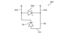
- FIG. 42B is an equivalent circuit of the semiconductor light emitting device according to the sixth embodiment.
- FIG. 43A is a schematic cross-sectional view showing the overall configuration of the semiconductor light emitting device according to the seventh embodiment.
- FIG. 43B is an equivalent circuit of the semiconductor light emitting device according to the seventh embodiment.
- FIG. 44 is a schematic cross-sectional view showing the overall configuration of the semiconductor light emitting device according to the eighth embodiment.
- each figure is a schematic diagram and is not necessarily exactly illustrated. Therefore, the scales and the like do not always match in each figure.
- the same reference numerals are given to substantially the same configurations, and duplicate explanations will be omitted or simplified.
- the terms “upper” and “lower” do not refer to the upward direction (vertically upward) and the downward direction (vertically downward) in absolute spatial recognition, but are based on the stacking order in the laminated configuration. It is used as a term defined by the relative positional relationship. Also, the terms “upper” and “lower” are used not only when the two components are spaced apart from each other and another component exists between the two components, but also when the two components are present. It also applies when they are placed in contact with each other.
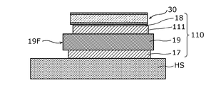
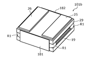
- FIGS. 1 and 2 are a schematic perspective view and a sectional view of the semiconductor light emitting device 1 according to the present embodiment, respectively.
- FIG. 2 is a cross-sectional view taken along the line II-II of FIG.
- the semiconductor light emitting device 1 includes a semiconductor light emitting chip 30 and a first submount 10.
- the semiconductor light emitting device 1 further includes a plurality of metal wires 91.
- the semiconductor light emitting chip 30 is an example of a first semiconductor light emitting chip arranged on the first submount 10.
- the semiconductor light emitting chip 30 is a semiconductor laser diode chip having a first electrode 31, a second electrode 32, and a laminate 39, and is mounted on the first submount 10. Will be implemented.
- the semiconductor light emitting chip 30 is arranged in the central portion of the first submount 10.
- the laminated body 39 has a substrate and a semiconductor laminated portion including a light emitting layer.
- the substrate is made of, for example, InP, GaAs, GaN, AlN, or the like. In this embodiment, the substrate is an n-type semiconductor substrate.
- the semiconductor laminated portion has, for example, an n-type clad layer, an n-side guide layer, a quantum well active layer, a p-side guide layer, and a p-type clad layer that are sequentially laminated on a substrate.
- the first electrode 31 is arranged on the main surface of the laminate 39 on the semiconductor laminated portion side, and the second electrode 32 is arranged on the main surface of the substrate side.
- the semiconductor light emitting chip 30 is bonded to the first submount 10 at the first electrode 31 arranged in the semiconductor laminated portion. That is, the semiconductor light emitting chip 30 is junction-down bonded to the first submount 10.
- the first electrode 31 is thermally and electrically connected to the spacer 11 included in the first submount 10.
- the semiconductor light emitting chip 30 has a first surface 30a, a second surface 30b, an exit surface 30F, and a rear surface 30R.
- the first surface 30a is a portion of the surface of the semiconductor light emitting chip 30 facing the first submount 10.
- the first electrode 31 has a first surface 30a. That is, the semiconductor laminated portion of the semiconductor light emitting chip 30 is arranged on the first surface 30a side of the semiconductor light emitting chip 30 with respect to the substrate.
- the second surface 30b is a surface opposite to the first surface 30a.
- the second electrode 32 has a second surface 30b.
- the semiconductor light emitting chip 30 has an optical waveguide WG extending in the first direction D1 parallel to the first surface 30a.
- the optical waveguide WG is arranged closer to the first surface 30a than the second surface 30b.
- the optical waveguide WG is an example of the first optical waveguide.
- the semiconductor laminated portion of the laminated body 39 of the semiconductor light emitting chip 30 has, for example, a light confinement structure composed of a ridge extending in the first direction D1 in the p-type clad layer.
- an optical waveguide WG having a light confinement structure is formed in the second direction D2.
- the optical waveguide WG is arranged on the first surface 30a side of the semiconductor light emitting chip 30 with respect to the substrate.
- the optical waveguide WG is formed, for example, in the center of the second direction D2 in the semiconductor laminated portion.
- the second direction D2 is a direction parallel to the first surface 30a and orthogonal to the first direction D1.
- the emission surface 30F is one of the side surfaces connecting the first surface 30a and the second surface 30b that intersects the first direction D1, and is an example of a first emission surface that emits emitted light in the first direction D1. Is. In the present embodiment, the emitted light is emitted from the position corresponding to the optical waveguide WG on the emitting surface 30F.
- the emitted light is, for example, a laser beam of any one of ultraviolet light, visible light, and infrared light having a peak wavelength between 250 nm and 20 ⁇ m.
- the rear surface 30R is an example of a third rear surface which is the other side surface that intersects the first direction D1 among the side surfaces connecting the first surface 30a and the second surface 30b.
- the rear surface 30R is a side surface facing the exit surface 30F of the semiconductor light emitting chip 30.
- the emission surface 30F and the rear surface 30R form a laser resonator, and the laser beam resonates in the optical waveguide WG.
- the point corresponding to the optical waveguide WG on the emission surface 30F, that is, the point at which the emitted light is emitted is referred to as a light emitting point 30e.
- the first submount 10 is a base on which the semiconductor light emitting chip 30 is arranged.
- the first submount 10 also functions as a heat sink from which the heat generated by the semiconductor light emitting chip 30 is discharged.
- the first submount 10 has a first base 19, a spacer 11, a second metal material 12, and a bonding material 18. Further, as shown in FIG. 2, the first submount 10 further has a back metal material 17.
- the first base 19 is the main member of the first submount 10.
- the first base 19 has a third surface 19a, on which the spacer 11 and the second metal material 12 are arranged.
- the first base 19 is an example of a first insulating material made of an insulating material.
- the first base 19 is made of, for example, a ceramic substrate, a polycrystalline substrate, a single crystal substrate or the like made of a material having high thermal conductivity such as alumina, AlN, SiC, or diamond.
- the first base 19 may be a composite material of a conductive material and an insulating material formed on the third surface 19a side.
- the first base 19 may be, for example, a substrate having an oxide film formed on the surface of a silicon substrate.
- the first base 19 may include an insulating material.
- the first base 19 has a back side surface 19b which is a surface opposite to the third surface 19a, and the back side metal material 17 is arranged on the back side surface 19b.
- the spacer 11 is an example of a first metal material arranged on the third surface 19a.
- the spacer 11 is arranged at least between the third surface 19a of the first base 19 and the first surface 30a of the semiconductor light emitting chip 30.
- the spacer 11 covers at least the central portion of the third surface 19a.
- the spacer 11 is electrically connected to the first surface 30a of the semiconductor light emitting chip 30 via the bonding material 18.
- the semiconductor light emitting chip 30 is junction-down bonded to the first submount 10 so that the first surface 30a faces the spacer 11.
- the spacer 11 is, for example, a plate-shaped metal material in which a metal having a high thermal conductivity such as Cu is used as a main component and a protective metal film such as Ni or Au is formed on the surface thereof.
- the second metal material 12 is a metal material arranged on the third surface 19a.
- the second metal material 12 is electrically insulated from the spacer 11 and electrically connected to the second electrode 32 of the semiconductor light emitting chip 30.
- the second metal material 12 and the second electrode 32 are electrically connected via the metal wire 91.
- the second metal material 12 is arranged apart from the spacer 11 in the second direction D2.
- the second metal material 12 is, for example, a plate-shaped metal material in which a metal having a high thermal conductivity such as Cu is used as a main component and a protective metal film such as Ni or Au is formed on the surface thereof.
- the joining material 18 is a metal material that joins the spacer 11 and the semiconductor light emitting chip 30.
- the bonding material 18 is arranged on the surface of the spacer 11 facing the semiconductor light emitting chip 30.
- the bonding material 18 is formed of, for example, AuSn or the like.
- the back side metal material 17 is a metal material arranged on the back side surface 19b of the first base 19.
- the back metal material 17 is, for example, a plate-shaped metal material in which a metal having a high thermal conductivity such as Cu is used as a main component and a protective metal film such as Ni or Au is formed on the surface thereof.
- the back metal material 17 is connected to a heat radiating member such as a heat sink.
- the metal wire 91 is a metal wire that connects the second electrode 32 of the semiconductor light emitting chip 30 and the second metal material 12 of the first submount 10.
- the metal wire 91 is formed of, for example, Au.
- the semiconductor light emitting device 1 includes the above-mentioned components, and each of the spacer 11 and the second metal material 12 is connected to an external wiring by a metal wire or the like (not shown). As a result, electric power can be supplied to the semiconductor light emitting device 1 from the outside.
- the emission surface 30F of the semiconductor light emitting chip 30 of the semiconductor light emitting device 1 the end surface 11F (that is, the left side surface of FIG. 2) in the spacer 11 of the first submount 10, and the first unit.
- the positional relationship between the table 19 and the first front surface 19F (that is, the left side surface of FIG. 2) will be described.
- the first front surface 19F is the end surface of the first base 19 in the first direction D1 that is closer to the exit surface 30F.
- the end surface 11F of the spacer 11 is an end surface located in the vicinity of the exit surface 30F of the spacer 11.
- the end surface 11F of the spacer 11 is the end surface of the two end surfaces of the spacer 11 in the first direction D1 that is closer to the exit surface 30F.
- the first front surface 19F is an end surface located in the vicinity of the exit surface 30F in the first base 19.
- the first front surface 19F is the end face of the first base 19 that is closer to the exit surface 30F among the two end faces of the first direction D1.
- the end face 11F and the first front surface 19F of the spacer 11 are end faces on the traveling direction side of the emitted light, and may be described as end faces on the emitting side of the emitted light.
- the end surface 11F and the first front surface 19F are arranged on the rear surface 30R side of the emission surface 30F in the first direction D1 with reference to the emission surface 30F of the semiconductor light emitting chip 30, (end surface 11F and first front surface 19F). Is expressed to be arranged behind the exit surface 30F (along the traveling direction of the emitted light).
- the end surface 11F and the first front surface 19F are arranged on the traveling direction side of the emitted light with respect to the emitting surface 30F, it is expressed that they are arranged in front of the emitting surface 30F (along the traveling direction of the emitted light).
- the emission surface 30F and the first front surface 19F are arranged on the rear surface 30R side of the end surface 11F in the first direction D1 when the end surface 11F of the spacer 11 is used as a reference, the end surface is arranged along the traveling direction of the emitted light. It is expressed that it is placed behind the 11th floor.
- the exit surface 30F and the first front surface 19F are arranged on the traveling direction side of the emitted light with respect to the end surface 11F, it is expressed that they are arranged in front of the end surface 11F along the traveling direction of the emitted light. Further, when the emission surface 30F and the end surface 11F are arranged on the rear surface 30R side of the first front surface 19F in the first direction D1 when the first front surface 19F is used as a reference, the first surface is along the traveling direction of the emitted light. It is expressed that it is arranged behind the front 19F.
- the exit surface 30F and the end surface 11F are arranged on the traveling direction side of the emitted light with respect to the first front surface 19F, it is expressed that they are arranged in front of the first front surface 19F along the traveling direction of the emitted light. .. In either case, when it is described as simply placed in front of or behind the reference surface, it is placed in front of or behind the reference surface along the traveling direction of the emitted light. Means that.
- the distance between the rear surface 30R and the first rear surface 19R, which is the rear end surface of the first base 19, is longer than the distance between the exit surface 30F and the first front surface 19F.
- the positional relationship between the components is determined so that the utilization efficiency of the emitted light can be enhanced.
- the emitted light which is a laser beam
- high-power light is required. Therefore, it is required to guide the emitted light to the irradiation target with the highest possible utilization efficiency. Therefore, it is necessary to avoid placing an opaque object that causes a loss of the emitted light in the optical path of the emitted light.
- the emitted light emitted from the semiconductor light emitting device 1 has an angle with respect to the optical axis Ax, which is a direction perpendicular to the emitting surface 30F, that is, a light intensity distribution with respect to the emission angle. Approximately, the light intensity is highest near the optical axis and has a Gaussian distribution with respect to the emission angle. As shown in FIG. 2, the spreading angle (full-width) of the emitted light of the semiconductor light emitting device 1 in the fast axis direction (that is, the vertical direction in FIG. 2) is 2 ⁇ f. At this time, from the lower outermost ray (the light ray indicated by the broken line Lb below the optical axis Ax in FIG.
- the light beam (indicated by) is a light ray having an intensity of less than 1% of the peak light intensity of the emitted light.
- the fast axis of the divergence angle corresponding to 1 / e 2 of the peak intensity, 40 ° or more, in the range of than 50 °.
- the spreading angle of the outermost light beam is in the range of 62 ° (equivalent to NA0.52) or more and 76 ° (equivalent to NA0.62) or less.
- the optical element When the light emitted from the semiconductor light emitting chip 30 is propagated by using the optical element, in order to obtain high-intensity light, it is necessary to combine the emitted light from the semiconductor light emitting chip 30 with the optical element with high efficiency. .. Therefore, it is necessary to reduce the irradiation of the outermost light beam having a spreading angle of 76 ° to a part of the semiconductor light emitting device 1 such as the first submount 10.
- the exit surface 30F is arranged in front of the end surface 11F of the spacer 11. Further, the first front surface 19F is arranged in front of the exit surface 30F (that is, on the left side in FIG. 2).
- the emission surface 30F in front of the end surface 11F of the spacer 11 in this way, the emission light emitted from the light emitting point 30e in the first direction D1 at a predetermined spread angle is blocked by the spacer 11. Can be suppressed. Therefore, it is possible to suppress a decrease in the utilization efficiency of the emitted light. Further, when the emitted light is incident on the optical element, it is possible to suppress a decrease in the coupling efficiency of the emitted light with the optical element.
- the first front surface 19F is arranged in front of the emitting surface 30F of the semiconductor light emitting chip 30, so that interference between the semiconductor light emitting chip 30 and the optical element occurs.
- the optical element can be fixed to the first front surface 19F while suppressing the above.
- the optical element is fixed to the first base 19 in this way, the accuracy of the fixing position of the optical element with respect to the semiconductor light emitting chip 30 is improved as compared with the case where the first submount 10 and the optical element are separated. Can be done. Therefore, the light emitted from the semiconductor light emitting chip 30 can be efficiently coupled to the optical element.
- the positional relationship between the first front surface 19F and the emission surface 30F for suppressing the emission light having the spread angle 2 ⁇ f as described above from being blocked by the first base 19 will be described.
- the distance Dy between the first surface 30a of the semiconductor light emitting chip 30 and the third surface 19a of the first base 19 and the distance Dz1 between the exit surface 30F and the first front surface 19F are used.
- the condition that the outermost light beam of the emitted light is not blocked by the first base 19 can be expressed by the following inequality (1).
- the distance from the first surface 30a to the light emitting point 30e is sufficiently smaller than the distance from the third surface 19a to the first surface 30a.
- the semiconductor light emitting device and the light source device using the semiconductor light emitting device according to the first modification of the first embodiment will be described.
- the semiconductor light emitting device according to the present modification further includes a bonding preliminary film in addition to the semiconductor light emitting device 1 according to the first embodiment.
- the light source device according to the present modification further includes a lens optical element in addition to the semiconductor light emitting device according to the present modification.
- the semiconductor light emitting device and the light source device according to this modification will be described focusing on the differences from the semiconductor light emitting device 1 according to the first embodiment.
- FIG. 3 is a schematic cross-sectional view showing the configurations of the semiconductor light emitting device 1a and the light source device 102 according to the present modification.
- FIG. 3 a cross section at a position similar to the cross section of the semiconductor light emitting device 1 shown in FIG. 2 is shown.
- the semiconductor light emitting device 1a includes a semiconductor light emitting chip 30, a first submount 10, and a bonding preliminary film 85c.
- the light source device 102 includes a semiconductor light emitting device 1a and a lens optical element 80.
- the light source device 102 further includes a bonding preliminary film 85a and a bonding material 85b for fixing the lens optical element 80 to the first submount 10, and a heat radiating member 9 in which the semiconductor light emitting device 1a is arranged.
- the semiconductor light emitting device 1a is fixed to the heat radiating member 9 made of Cu or the like by a second bonding material 16 made of solder or the like.
- the lens optical element 80 is an element connected to the first submount 10, and the emitted light from the semiconductor light emitting chip 30 is incident on the lens optical element 80.
- the lens optical element 80 is arranged forward with respect to the first submount 10 along the traveling direction of the emitted light, and is connected to the first submount 10.
- the lens optical element 80 is fixed to the first front surface 19F by the joint portion 85.
- the lens optical element 80 is a fast-axis collimator lens and collimates the emitted light in the fast-axis direction.
- the lens optical element 80 for example, a cylindrical lens can be used.
- the fast axis direction is a direction perpendicular to the first surface 30a of the semiconductor light emitting chip 30 (that is, the vertical direction in FIG. 3).
- the lens optical element 80 is arranged so that the focal length f of the lens optical element 80 and the distance from the principal point of the lens optical element 80 to the emission surface 30F of the semiconductor light emitting chip 30 are equal to each other. Will be done.
- the lens optical element 80 has an incident surface 80a facing the emission surface 30F of the semiconductor light emitting chip 30.
- the joint portion 85 is a member that joins the first submount 10 and the lens optical element 80.
- the joint portion 85 has a joint preliminary membranes 85a and 85c and a joint material 85b.
- the bonding preliminary films 85a and 85c are films arranged on the incident surface 80a of the lens optical element 80 and the first front surface 19F, respectively.
- the preliminary bonding films 85a and 85c are composed of, for example, a multilayer metal film such as Ni, Ti, Pt, and Au.
- the components and stacking order of the multilayer metal films constituting the bonding preliminary films 85a and 85c are appropriately selected according to the materials of the lens optical element 80, the first base 19 and the bonding material 85b so as to realize a strong bonding. It should be done.
- each of the bonding preliminary films 85a and 85c is a multilayer metal film in which a Ni film and an Au film are laminated in order from the farthest from the bonding material 85b, respectively.
- the bonding material 85b is composed of, for example, a solder material such as AuSn, SnAgCu, SnSb.
- the bonding preliminary film 85a is formed in advance on the incident surface 80a of the lens optical element 80.
- the bonding preliminary film 85c is preformed on the first front surface 19F.
- the bonding material 85b is preformed on either the incident surface 80a or the first front surface 19F. In the present embodiment, it is formed on the first front surface 19F.
- the lens optical element 80 is arranged at a predetermined position on the first base 19, and the optical axis is adjusted, and the bonding material 85b and the bonding preliminary film 85a are brought into close contact with each other.
- the first submount 10 is heated while the optical axis adjustment of the lens optical element 80 is completed.
- the joint material 85b of the joint portion 85 is melted.
- the bonding material 85b is solidified, and the lens optical element 80 is fixed to the first base 19.
- the utilization efficiency of the emitted light can be improved. Further, by defining the positional relationship between the emission surface 30F and the first front surface 19F so that the above-mentioned inequality (1) holds, it is possible to suppress the emission light from being blocked by the first base 19. Thereby, the utilization efficiency of the emitted light in the semiconductor light emitting device 1a according to the present modification can be further improved. In this case, almost all of the emitted light is incident on the lens optical element 80, becomes light collimated by the lens optical element 80 (laser light in this modification), and is emitted from the lens optical element 80.
- the emission surface 30F is arranged behind the first front surface 19F. Therefore, in the light source device 102, the lens optical element 80 can be fixed by using the first front surface while maintaining the distance between the emission surface 30F and the lens optical element 80 at a predetermined size. Therefore, it is possible to suppress the interference between the semiconductor light emitting chip 30 and the lens optical element 80. Further, by fixing the lens optical element 80 to the first base 19, the distance between the lens optical element 80 and the exit surface 30F can be minimized, so that the degree of freedom in the optical design of the lens optical element 80 can be increased. Can be improved. Further, since the semiconductor light emitting chip 30 and the lens optical element 80 can be fixed to the same first base 19, the positional relationship between the semiconductor light emitting chip 30 and the lens optical element 80 changes after the lens optical element 80 is fixed. It is possible to suppress changes over time.
- the semiconductor light emitting device 1a it is possible to suppress the emitted light from being blocked by the spacer 11 as in the semiconductor light emitting device 1 according to the first embodiment. Further, by determining the positional relationship between the semiconductor light emitting chip 30 and the first base 19 so that the above inequality (1) holds, it is possible to prevent the emitted light from being blocked by the first base 19.
- the lens optical element 80 which is a fast-axis collimator lens
- the distance Dz4 between the first front surface of the first base 19 and the emission surface 30F of the semiconductor light emitting chip 30 may be, for example, 10 ⁇ m or more.
- the fast axis of the emitted light emitted as collimated light from the lens optical element 80 of the semiconductor light emitting device 1a.
- the beam width in the direction can be, for example, a small beam width of 200 ⁇ m or more and 400 ⁇ m or less. In order to obtain such a small beam width, it is necessary to shorten the focal length f of the lens optical element 80.
- the thickness (sag) Dz5 of the lens optical element 80 in the outermost light beam should be thin in order to shorten the focal length f of the lens optical element 80, but the structural strength of the lens optical element 80 is ensured. For that purpose, it is better to be thick. In order to achieve both a short focal length f and an intensity, the thickness Dz5 can be, for example, 100 ⁇ m or more and 200 ⁇ m or less.
- the distance Dz4 is expressed by the following equation (2).
- a material having a refractive index n of 1.5 or more and 1.8 or less is selected as the material constituting the lens optical element 80, so that the distance Dz4 may be 13 ⁇ m or more and 200 ⁇ m or less.
- the distance Dz1 that is, the distance Dz4 in the first direction between the first front surface 19F and the exit surface is 13 ⁇ m or more and 200 ⁇ m or less. All you need is.
- the distance Dy may be 10 ⁇ m or more and 163 ⁇ m.
- the thickness of the bonding material 18 is sufficiently thin with respect to the thickness of the spacer 11
- the distance Dy can be regarded as the thickness of the spacer 11. Therefore, the thickness of the spacer 11 may be 10 ⁇ m or more and 163 ⁇ m.
- FIGS. 4A to 4D are schematic views illustrating each step of the manufacturing method of the first submount 10, the bonding preliminary film 85c, and the bonding material 85b according to the present modification, respectively.
- FIG. 5 is a schematic diagram illustrating a process of attaching the lens optical element 80 to the first submount 10 according to the present modification.
- the base material 19M of the first base 19 is prepared.
- a ceramic plate such as AlN, SiC, or diamond having a predetermined thickness is prepared as the base material 19M.
- the thickness of the base material 19M is, for example, about 50 ⁇ m to 1000 ⁇ m.
- a metal film such as Ti, Pt, Au is formed on one main surface of the base material 19M (the upper main surface in FIG. 4A), and then patterning is performed.
- a metal film such as Ti, Pt, and Au is formed on the other main surface (lower main surface in FIG. 4A) of the base metal 19M, and then patterning is performed.
- a metal such as Cu is formed on the patterned metal film on both sides of the base metal 19M by electrolytic plating or the like.
- the thickness of a metal such as Cu is, for example, about 10 to 200 ⁇ m. As a result, a plurality of spacers 11 can be formed on the base metal 19M.
- the second metal material 12 is also formed at the same time on the main surface on which the spacer 11 of the base material 19M is formed. Further, a plurality of backside metal materials 17 are also formed on the other main surface of the base material 19M at the same time.
- a protective metal film composed of Cr, Ni, Au, etc. is subsequently formed on the surfaces of the spacer 11, the second metal material 12, and the back metal material 17 by vapor deposition or the like. Then, a patterned bonding material 18 is formed on a part of each of the plurality of spacers 11.
- vapor deposition using a metal mask, selective electrolytic plating, or the like can be selected.
- the base metal 19M is divided (that is, individualized) into a plurality of first bases 19 by dicing. Thereby, the first submount 10 can be formed.
- the first submount 10 is sandwiched between the T-shaped jig 99, and only a part of the first front surface 19F is exposed from the jig 99.
- a metal film such as Ti, Pt, and Au is formed on the exposed first front surface 19F by vapor deposition or the like to form a bonding preliminary film 85c.
- a bonding material 85b composed of a solder material such as AuSn is formed on the surface of the bonding preliminary film 85c by vapor deposition, plating, or the like.
- the semiconductor light emitting chip 30 is arranged on the bonding material 18 of the first submount 10, and the second electrode 32 of the semiconductor light emitting chip 30 and the second metal material 12 are connected to the metal wire 91. Connect with. Thereby, the semiconductor light emitting device 1 according to the first embodiment can be formed.
- a bonding preliminary film 85c (not shown in FIG. 5) and a bonding material 85b are formed on the first front surface 19F.
- the lens optical element 80 is prepared as a member constituting the light source device.
- a bonding preliminary film 85a having the same structure as the bonding preliminary film 85c is formed by selective vapor deposition or the like.
- the bonding preliminary film 85a and the bonding material 85b are bonded.
- the lens optical element 80 is fixed to the first base 19 in a state where the optical axis is adjusted.
- the semiconductor light emitting device 1a according to this modification can be manufactured. According to the above manufacturing method, by using the semiconductor light emitting device 1a according to the present modification, the optical axis of the lens optical element 80 constituting the light source device can be easily adjusted, and the manufacturing of the light source device is facilitated. can.
- the semiconductor light emitting device according to the second embodiment will be described.
- the semiconductor light emitting device according to the present embodiment is different from the semiconductor light emitting device 1 according to the first embodiment in that it mainly includes a second submount in addition to the first submount.
- the semiconductor light emitting device according to the present embodiment will be described focusing on the differences from the semiconductor light emitting device 1 according to the first embodiment.
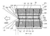
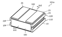
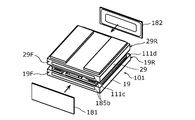
- FIGS. 6 to 10B are a schematic perspective view, a first sectional view and a second sectional view showing the overall configuration of the semiconductor light emitting device 101 according to the present embodiment, respectively. 7 and 8 are cross-sectional views taken along the line VII-VII and VIII-VIII of FIG. 6, respectively.
- FIG. 9 is an exploded perspective view of the semiconductor light emitting device 101 according to the present embodiment.
- FIG. 10A is a schematic perspective view showing the configuration of the second submount 120 and the members connected to the second submount 120 according to the present embodiment.
- FIG. 10B is a schematic perspective view showing the configuration of the semiconductor light emitting chip 30 according to the present embodiment.
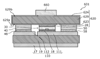
- the semiconductor light emitting device 101 includes a first submount 110, a semiconductor light emitting chip 30, and a second submount 120.
- the semiconductor light emitting device 101 further includes a first side wall 40 and a second side wall 50.
- the semiconductor light emitting device 101 is fixed to a heat radiating member (not shown) by a second bonding material (not shown).
- the heat radiating member is arranged on the back side metal material 17 of the first submount 110, and the back side metal material 17 of the first submount 110 and the heat radiating member are joined by the second joining material.
- the semiconductor light emitting chip 30 has the same configuration as the semiconductor light emitting chip 30 according to the first embodiment. As shown in FIG. 10B, the semiconductor light emitting chip 30 has a first surface 30a and a second surface 30b, and has an optical waveguide WG extending in the first direction D1 parallel to the first surface 30a.
- the first submount 110 has a first base 19, a spacer 111, a second metal material 112, a bonding material 18, and a back metal material 17.
- the first submount 110 further comprises joins 48 and 58.
- the spacer 111 is an example of a first metal material arranged on the third surface 19a of the first base 19.
- the spacer 111 is arranged at least between the third surface 19a of the first base 19 and the first surface 30a of the semiconductor light emitting chip 30.
- the spacer 111 covers at least the central portion of the third surface 19a.
- the spacer 111 is thermally and electrically connected to the first surface 30a of the semiconductor light emitting chip 30 via the bonding material 18.
- the semiconductor light emitting chip 30 is junction-down bonded to the first submount 110 so that the first surface 30a faces the spacer 111.
- the spacer 111 is, for example, a plate-shaped metal material having a metal having high thermal conductivity such as Cu as a main component and having a protective metal film such as Au formed on the surface thereof.
- the spacer 111 is an edge (that is, a front edge) arranged in the vicinity of the emission surface 30F of the semiconductor light emitting chip 30 in the top view of the third surface 19a of the first base 19.
- the spacer 111 is recessed inward from the two end edges of the spacer in the first direction, whichever is closer to the exit surface 30F. It has one recess 111c.
- the first recess 111c is arranged at the end of the spacer 111 on the side farther from the second metal material 112 in the second direction D2.
- the first recess 111c is located on the rear surface 30R side (that is, the front edge) from the end surface 111F (that is, the front edge) arranged in the vicinity of the emission surface 30F of the semiconductor light emitting chip 30 in the spacer 111 in the top view of the third surface 19a. It is a part that is dented to the rear).
- the first recess 111c and each recess described later can be used as a space for arranging the bonding material when, for example, an optical element or the like is fixed to the first base 19 and the second base 29.
- the spacer 111 is recessed inward from the edge (that is, the rear edge) arranged in the vicinity of the rear surface 30R in the top view of the third surface 19a of the first base 19.
- the third concave portion 111d is recessed from the end surface 111R (that is, the rear end edge) arranged in the vicinity of the rear surface 30R of the spacer 111 to the exit surface 30F side (that is, the front) in the top view of the third surface 19a. It is a part.
- the third recess 111d is arranged at the end of the spacer 111 on the side farther from the second metal material 112 in the second direction D2.
- the second metal material 112 is a metal material arranged on the third surface 19a.
- the second metal material 112 is electrically insulated from the spacer 111 and electrically connected to the second electrode 32 of the semiconductor light emitting chip 30.
- the second metal material 112 is electrically connected to the second electrode 32 via the joining material 48, the first side wall 40, the third metal material 23 of the second submount 120, and the joining material 28. Will be done.
- the second metal material 112 is arranged apart from the spacer 111 in the second direction D2.
- the second metal material 112 is, for example, a plate-shaped metal material containing a metal having a high thermal conductivity such as Cu as a main component and having a protective metal film such as Ni or Au formed on the surface thereof.
- the second metal material 112 has an edge (that is, a front edge) arranged in the vicinity of the exit surface 30F in the top view of the third surface 19a of the first base 19. It has a second recess 112c that is recessed inward from the second metal material 112.
- the second metal material 112 in the top view of the third surface 19a, has a second metal at the end edge of the two end edges of the second metal material 112 in the first direction D1 that is closer to the exit surface 30F. It has a second recess 112c that is recessed inward from the material 112.
- the second recess 112c is located on the rear surface 30R side (that is, rearward) from the end surface 112F (that is, the front edge) arranged in the vicinity of the exit surface 30F of the second metal material 112 in the top view of the third surface 19a. It is a dented part.
- the second recess 112c is arranged at the end of the second metal material 112 on the side far from the spacer 111 in the second direction D2.
- the second metal material 112 has the second metal material 112 at the edge (that is, the rear edge) arranged in the vicinity of the rear surface 30R in the top view of the third surface 19a of the first base 19. It has a fourth recess 112d that is recessed inward.
- the fourth recess 112d is located on the exit surface 30F side (that is, the front) from the end surface 112R (that is, the rear edge) arranged in the vicinity of the rear surface 30R of the second metal material 112 in the top view of the third surface 19a. It is a dented part.
- the fourth recess 112d is arranged at the end of the second metal material 112 on the side far from the spacer 111 in the second direction D2.
- the second submount 120 is a member arranged on the second surface 30b of the semiconductor light emitting chip 30.
- the second submount 120 functions as a heat sink from which the heat generated by the semiconductor light emitting chip 30 is discharged.
- the second submount 120 includes a second base 29, a third metal material 23, a fourth metal material 24, a fifth metal material 25, a sixth metal material 26, and a bonding material. It has 28 and.
- the semiconductor light emitting device 101 includes a first side wall 40 and a second side wall 50 connected to the second submount 120. In the present embodiment, as shown in FIGS. 9 and 10A, the first side wall 40 and the second side wall 50 are previously attached to the second submount 120.
- a joining material 48 and a joining material 58 are attached to a part of the surface of the first side wall 40 and the second side wall 50, respectively.
- the second base 29 is the main member of the second submount 120.
- the second base 29 has a fourth surface 29a and a fifth surface 29b which is a surface opposite to the fourth surface 29a.
- the second base 29 has one or more first vias penetrating between the second insulating material made of an insulating material and the fourth surface 29a and the fifth surface 29b of the second base 29. Includes B1 and one or more second vias B2.
- the second base 29 has three first vias B1 arranged in the first direction D1 and three second vias arranged in the first direction D1. It has a via B2.
- the second insulating material of the second base 29 is made of, for example, a ceramic substrate, a polycrystalline substrate, a single crystal substrate or the like made of a material having a high thermal conductivity such as alumina, AlN, SiC, or diamond. Further, one or more first vias B1 and one or more second vias B2 are through electrodes made of a metal material formed in holes penetrating between the fourth surface 29a and the fifth surface 29b of the second base 29. It is made of a metal material such as W, Mo, Cu, and Au. A third metal material 23 and a fourth metal material 24 are arranged on the fourth surface 29a of the second base 29. Further, the joining material 28 is arranged on the third metal material 23.
- a fifth metal material 25 and a sixth metal material 26 are arranged on the fifth surface 29b of the second base 29.
- the third metal material 23, the fourth metal material 24, the fifth metal material 25, and the sixth metal material 26 are mainly composed of a metal having a high thermal conductivity such as Cu, and have a protective metal such as Ni and Au on the surface. It is a plate-shaped metal material on which a film is formed.
- the third metal material 23 is a metal material arranged on the fourth surface 29a of the second base 29.
- the second surface 30b of the semiconductor light emitting chip 30 faces the third metal material 23.
- the third metal material 23 is arranged at least between the fourth surface 29a of the second base 29 and the second surface 30b of the semiconductor light emitting chip 30.
- the third metal material 23 is thermally and electrically connected to the second surface 30b of the semiconductor light emitting chip 30 via the bonding material 28. In this way, the semiconductor light emitting chip 30 is joined to the second submount 120 so that the second surface 30b faces the third metal material 23. Further, the third metal material 23 is connected to the first side wall 40.
- the joining material 28 is a metal material that joins the third metal material 23 and the semiconductor light emitting chip 30.
- the bonding material 28 is arranged on the surface of the third metal material 23 facing the semiconductor light emitting chip 30.
- the bonding material 28 is formed of, for example, AuSn or the like.
- the third metal material 23 is an edge (that is, a front edge) arranged in the vicinity of the exit surface 30F in the top view of the fourth surface 29a of the second base 29.
- the end surface 23F has a fifth recess 23c recessed inward from the third metal material 23.
- the end face 23F is the end face of the third metal material 23 that is closer to the exit surface 30F among the two end faces in the first direction D1.
- the fifth recess 23c is located on the rear surface 30R side (that is, rearward) from the end surface 23F (that is, the front edge) arranged in the vicinity of the exit surface 30F of the third metal material 23 in the top view of the fourth surface 29a. It is a dented part.
- the fifth recess 23c is arranged at the end of the third metal material 23 on the side far from the fourth metal material 24 in the second direction D2.
- the third metal material 23 has a third metal material 23 on the edge (that is, the rear edge) arranged in the vicinity of the rear surface 30R in the top view of the fourth surface 29a of the second base 29. It has a seventh recess 23d that is recessed inward.
- the seventh recess 23d is located on the exit surface 30F side (that is, the front) from the end surface 23R (that is, the rear edge) arranged in the vicinity of the rear surface 30R of the third metal material 23 in the top view of the fourth surface 29a. It is a dented part.
- the seventh recess 23d is arranged at the end of the third metal material 23 on the side far from the fourth metal material 24 in the second direction D2.
- the fourth metal material 24 is a metal material arranged on the fourth surface 29a of the second base 29.
- the fourth metal material 24 is electrically insulated from the third metal material 23 and electrically connected to the first electrode 31 of the semiconductor light emitting chip 30. As shown in FIG. 7, the fourth metal material 24 is arranged apart from the third metal material 23 in the second direction D2.
- the fourth metal material 24 has an edge (that is, a front edge) arranged in the vicinity of the exit surface 30F in the top view of the fourth surface 29a of the second base 29. It has a sixth recess 24c that is recessed inward from the fourth metal material 24.
- the sixth recess 24c is located on the rear surface 30R side (that is, rearward) from the end surface 24F (that is, the front edge) arranged in the vicinity of the exit surface 30F of the fourth metal material 24 in the top view of the fourth surface 29a. It is a dented part.
- the sixth recess 24c is arranged at the end of the fourth metal material 24 on the side far from the third metal material 23 in the second direction D2.
- the fourth metal material 24 has a fourth metal material 24 on the edge (that is, the rear edge) arranged in the vicinity of the rear surface 30R in the top view of the fourth surface 29a of the second base 29. It has an eighth recess 24d that is recessed inward.
- the eighth recess 24d is located on the exit surface 30F side (that is, the front) from the end surface 24R (that is, the rear edge) arranged in the vicinity of the rear surface 30R of the fourth metal material 24 in the top view of the fourth surface 29a. It is a dented part.
- the eighth recess 24d is arranged at the end of the fourth metal material 24 on the side far from the third metal material 23 in the second direction D2.
- the fifth metal material 25 is a metal material arranged on the fifth surface 29b of the second base 29. As shown in FIG. 7, the fifth metal material 25 is arranged apart from the sixth metal material 26 in the second direction D2.
- the sixth metal material 26 is a metal material arranged on the fifth surface 29b of the second base 29.
- the sixth metal material 26 is electrically insulated from the fifth metal material 25 and electrically connected to the second electrode 32 of the semiconductor light emitting chip 30.
- the sixth metal material 26 is electrically connected to the second electrode 32 via the first via B1, the third metal material 23, and the bonding material 28. As shown in FIG. 7, the sixth metal material 26 is arranged apart from the fifth metal material 25 in the second direction D2.
- the first side wall 40 and the second side wall 50 are members connected to the second submount 120. In the present embodiment, as shown in FIG. 7, the first side wall 40 and the second side wall 50 are arranged in the second direction.
- the semiconductor light emitting chip 30 is arranged between the first side wall 40 and the second side wall 50.
- the first side wall 40 includes a first metal column electrically connected to the second metal material 112 and the third metal material 23.
- the second side wall 50 includes a second metal column electrically connected to the spacer 111 and the fourth metal material 24.
- the first metal column is electrically connected to the second metal material 112 via the bonding material 48, and is directly connected to the third metal material 23.
- the second metal column is electrically connected to the spacer 111 via the bonding material 58, and is directly connected to the fourth metal material 24.
- the first side wall 40 includes only the first metal pillar, but may include a member other than the first metal pillar.
- the second side wall 50 includes only the second metal pillar, but may include a member other than the second metal pillar.
- the first side wall 40 and the second side wall 50 may include an insulating member.
- the first metal column and the second metal column are formed of a material having high thermal conductivity and high electrical conductivity, such as Cu, Ni, Al, and Au.
- the first metal column and the second metal column are metal columns in which a metal film for protecting Ni and Au is formed on the surface of a Cu column formed by electrolytic plating.
- the first side wall 40 (that is, the first metal column) has a substantially square columnar shape having a length equivalent to that of the semiconductor light emitting chip 30 in the first direction D1. As shown in FIG. 10A, the first side wall 40 is located at the edge (that is, the front edge) arranged in the vicinity of the exit surface 30F in the top view of the fourth surface 29a of the second base 29.
- One side wall 40 has a ninth recess 40c recessed inward.
- the ninth concave portion 40c is from the end surface 40F (that is, the front end edge) arranged in the vicinity of the exit surface 30F on the first side wall 40 to the rear surface 30R side (that is, the rear side) in the top view of the fourth surface 29a.
- the ninth recess 40c is arranged at the end of the first side wall 40 on the side far from the second side wall 50 in the second direction D2. Further, the first side wall 40 faces inward of the first side wall 40 at the end edge (that is, the rear end edge) arranged in the vicinity of the rear surface 30R in the top view of the fourth surface 29a of the second base 29. It has an eleventh recess 40d recessed in.
- the eleventh recess 40d is from the end surface 40R (that is, the rear end edge) arranged in the vicinity of the rear surface 30R on the first side wall 40 to the exit surface 30F side (that is, the front) in the top view of the fourth surface 29a. It is a dented part.
- the eleventh recess 40d is arranged at the end of the first side wall 40 on the side far from the second side wall 50 in the second direction D2.
- the second side wall 50 (that is, the second metal column) has a substantially square columnar shape having a length equivalent to that of the semiconductor light emitting chip 30 in the first direction D1.
- the second side wall 50 is located at the edge (that is, the front edge) arranged in the vicinity of the exit surface 30F in the top view of the fourth surface 29a of the second base 29.
- the second side wall 50 has a tenth concave portion 50c recessed inward.
- the tenth recess 50c is from the end surface 50F (that is, the front edge) arranged in the vicinity of the exit surface 30F on the second side wall 50 to the rear surface 30R side (that is, the rear) in the top view of the fourth surface 29a.
- the tenth recess 50c is arranged at the end of the second side wall 50 on the side far from the first side wall 40 in the second direction D2. Further, the second side wall 50 faces inward of the second side wall 50 at the end edge (that is, the rear end edge) arranged in the vicinity of the rear surface 30R in the top view of the fourth surface 29a of the second base 29. It has a twelfth recess 50d recessed in.
- the twelfth recess 50d is from the end surface 50R (that is, the rear edge) arranged in the vicinity of the rear surface 30R on the second side wall 50 to the exit surface 30F side (that is, the front) in the top view of the fourth surface 29a.
- the twelfth recess 50d is arranged at the end of the first side wall 40 on the side far from the first side wall 40 in the second direction D2.
- a joining material 48 is attached to the surface of the first side wall 40.
- a joining material 58 is attached to the surface of the second side wall 50.
- the joining material 48 is a metal material that joins the first side wall 40 and the second metal material 112.
- the joining material 48 is formed of, for example, AuSn or the like.
- the joining material 48 is arranged on the surface of the second metal material 112 facing the first side wall 40.
- the joining material 48 has a portion recessed inward in part in accordance with the ninth recess 40c and the eleventh recess 40d.
- the joining material 58 is a metal material that joins the spacer 111 and the second side wall 50.
- the joining material 58 is formed of, for example, AuSn or the like.
- the joining material 58 is arranged on the surface of the spacer 111 facing the second side wall 50.
- the joining material 58 has a portion recessed inward in part in accordance with the tenth recess 50c and the twelfth recess 50d.
- the fourth metal material 24 is electrically connected to the first electrode 31 via the second side wall 50, the joining material 58, the spacer 111 of the first submount 110, and the joining material 18. Therefore, the fifth metal material 25 is connected to the first electrode 31 via the second via B2, the fourth metal material 24, the second side wall 50, the joining material 58, the spacer 111 of the first submount 110, and the joining material 18. It is electrically connected.
- the sixth metal material 26 is electrically insulated from the fifth metal material 25 and electrically connected to the second electrode 32 of the semiconductor light emitting chip 30.
- the fifth metal material 25 and the sixth metal material 26 of the second submount 120 are each connected to an external power source by a metal wire or the like (not shown).
- the current input to the fifth metal material 25 is the second via B2 of the second submount 120, the fourth metal material 24, the second side wall 50 (second metal column), the joining material 58, and the spacer 111, joining. It is input to the first electrode 31 of the semiconductor light emitting chip 30 via the material 18.
- the current input to the semiconductor light emitting chip 30 is output from the second electrode 32 via the third metal material 23, the first via B1, and the sixth metal material 26.
- the method of electrically connecting the sixth metal material 26 and the third metal material 23 of the second submount 120, and the fifth metal material 25 and the fourth metal material 24 are connected.
- a method of electrically connecting a method of providing a first via B1 and a second via B2 penetrating the second base 29 is used, but the method is not limited thereto.
- a metal film is formed on the fourth surface, the side surface, and the fifth surface of the second base 29, the sixth metal material 26 and the third metal material 23 are electrically connected, and the fifth metal material 25 is formed.
- the fourth metal material 24 may be electrically connected.
- FIGS. 11A to 11D are schematic cross-sectional views showing each step of the manufacturing method of the semiconductor light emitting device 101 according to the present embodiment, respectively.
- 11A to 11D show a cross section perpendicular to the first surface 30a through the optical waveguide WG of the semiconductor light emitting chip 30.
- the first submount 110 is arranged on the heating stage HS, and the semiconductor light emitting chip 30 is arranged at a predetermined position on the first submount 110.
- the method for manufacturing the first submount 110 is the same as the method for manufacturing the first submount 10 according to the first modification of the first embodiment.
- a positioning jig JG having a surface roughness of 1 ⁇ m or less in Peak To Valley is prepared, and the surface of the positioning jig JG comes into contact with the first front surface 19F of the first base 19.
- the surface of the positioning jig JG in contact with the first front surface 19F is a flat surface and is perpendicular to the mounting surface of the heating stage HS (that is, the upper surface of the heating stage HS shown in FIG. 11B).
- the term "vertical" means not only a state of being completely vertical but also a state of being substantially vertical. For example, vertical means 85 ° or more and 95 ° or less.
- the second submount 120 is moved using the collet CL.
- the first side wall 40 and the second side wall 50 are attached to the second submount 120.
- the second front surface 29F which is an end surface (that is, the front end surface) arranged in the vicinity of the exit surface 30F of the second base 29 of the second submount 120, is a positioning jig.
- the jig is fixed.
- the second front surface 29F is the end surface of the second base 29 that is closer to the exit surface 30F among the two end surfaces of the first direction D1.
- the first submount 110 and the like are heated by the heating stage HS to melt each joint material.
- the semiconductor light emitting device 101 can be manufactured by solidifying each bonding material by cooling the heating stage HS. By such a manufacturing method, it is possible to keep the positional deviation between the first front surface 19F and the second front surface 29F in the first direction D1 to, for example, about 5 ⁇ m or less.
- the emission surface 30F of the semiconductor light emitting chip 30 may be arranged 10 ⁇ m or more behind the first front surface 19F so that the positioning jig JG and the emission surface 30F of the semiconductor light emitting chip 30 do not come into contact with each other. ..
- FIG. 12 is a schematic cross-sectional view showing the positional relationship between the components of the semiconductor light emitting device 101 according to the present embodiment.
- the emission surface 30F is the emission surface 30F side (that is, the front side) of the spacer 111, similarly to the semiconductor light emitting device 1 according to the first embodiment. ) Is located in front of the end surface 111F, and the first front surface 19F is located in front of the exit surface 30F.
- the semiconductor light emitting device 101 according to the present embodiment also has the same effect as the semiconductor light emitting device 1 according to the first embodiment.
- the relationship with the distance Dy to the third surface 19a of the table 19 is obtained in the same manner as the relationship between the distance Dz1 and the distance Dy according to the first embodiment.
- the distance Dz may be less than or equal to the distance Dy. This makes it possible to prevent the emitted light from being blocked by the first base 19 when the spreading angle (2 ⁇ f) of the emitted light is 90 ° or less.
- the second front surface 29F arranged in the vicinity (that is, forward) of the exit surface 30F in the second base 29 of the second submount 120 is located in front of the exit surface 30F.
- the second front surface 29F is arranged in front of the emitting surface 30F of the semiconductor light emitting chip 30, so that the semiconductor light emitting chip 30 interferes with the optical element.
- the optical element can be fixed to the second front surface 29F while suppressing the above.
- the optical element is fixed to the second base 29 in this way, the accuracy of the fixed position of the optical element with respect to the semiconductor light emitting chip 30 is improved as compared with the case where the second submount 120 and the optical element are separated. Can be done. Therefore, the light emitted from the semiconductor light emitting chip 30 can be efficiently coupled to the optical element.
- the second base 29 not only the second base 29 but also the first base 19 may be used.
- the first front surface 19F and the second front surface 29F may be in the same plane.
- the end face 23F and the second front surface 29F of the third metal material 23 are combined with each other.
- the positional relationship with the exit surface 30F can be determined in the same manner as the positional relationship between the first front surface 19F and the emission surface 30F in the first embodiment. That is, the relationship between the distance from the exit surface 30F to the end surface 23F and the distance from the first surface 30a to the second surface 30b, or the distance from the emission surface 30F to the second front surface 29F, and the distance from the first surface 30a to the first surface 30a. 4 It can be determined from the relationship with the distance to the surface 29a.
- the end surface 23F arranged on the exit surface 30F side (that is, the front) of the third metal material 23 is located in front of the exit surface 30F.
- the end surface 23F of the third metal material 23 is arranged behind the first front surface 19F and the second front surface 29F. As a result, it is possible to prevent the emitted light from being blocked by the third metal material 23. Further, by suppressing the distance from the exit surface 30F to the end surface 23F to about the distance from the third metal material 23 to the light emitting point 30e (that is, about the thickness of the semiconductor light emitting chip 30), the emitted light is the third metal material 23. It is possible to more reliably suppress the obstruction by.
- FIGS. 13 and 14 are a schematic first cross-sectional view and a second cross-sectional view illustrating the heat dissipation path of the semiconductor light emitting device 101 according to the present embodiment, respectively.
- 13 and 14 are cross-sectional views taken along the line VII-VII and VIII-VIII of FIG. 6, respectively. 13 and 14 show an outline of the heat dissipation path with arrows.
- part of the heat generated in the optical waveguide WG (particularly the active layer) of the semiconductor light emitting chip 30 is directly conducted to the first submount 110 and diffused in the second direction D2. However, it is arranged at a position facing the back surface 19b of the first submount 110, and is discharged to a heat dissipation member (not shown) connected to the first submount 110.
- the other part is conducted to the first submount 110 via the second submount 120 and the first side wall 40 and the second side wall 50. , Is discharged to a heat dissipation member (not shown).
- the first submount 110, the second submount 120, the first side wall 40 and the second side wall 50 are used, and the heat is generated in the optical waveguide WG of the semiconductor light emitting chip 30.
- the heat generated can be effectively dissipated.
- the third metal material 23 having a high thermal conductivity and a predetermined thickness is arranged in a portion close to the semiconductor light emitting chip 30. Therefore, the heat generated by the optical waveguide WG can be dissipated more effectively.
- a spacer 111 having a high thermal conductivity and a predetermined thickness is arranged in a portion of the semiconductor light emitting chip 30 close to the optical waveguide WG. Therefore, the heat generated by the optical waveguide WG can be dissipated more effectively.
- the first submount 110 has an insulating first base 19, a metal such as copper, which is a conductive material, can be used as a heat dissipation member. With this configuration, the positive electrode, the negative electrode, and the heat radiating member of the semiconductor light emitting chip 30 can be insulated from each other, and the heat generated by the semiconductor light emitting chip 30 can be effectively radiated.
- each heat dissipation path of the generated heat is indicated by an arrow.
- Part of the heat generated from any point is conducted to the first submount 110, and the other part is conducted to the second submount 120.
- at least a part of the heat conducted to the second submount 120 is conducted to the first submount 110 via the first side wall 40 and the second side wall 50.
- the heat generated at the point Y1 is conducted from the semiconductor light emitting chip 30 to the third metal material 23 of the second submount 120 and the second base 29.
- the end surface 23F of the third metal material 23 is located in front of the exit surface 30F
- the second front surface 29F is located in front of the end surface 23F. Therefore, since the heat generated at the point Y1 is conducted while diffusing forward in the second submount 120, the heat generated at the point Y1 can be effectively dissipated.
- the heat generated at the point Y4 near the rear surface 30R is conducted from the semiconductor light emitting chip 30 to the third metal material of the second submount 120 and the second base 29 on the second submount 120 side.
- the semiconductor light emitting chip 30 conducts to the spacer 111 of the first submount 110 and the first base 19.
- the semiconductor light emitting chip 30 has an emission surface 30F and a back surface 30R facing back.
- the first base 19 has a first rear surface 19R which is an end surface arranged in the vicinity of the rear surface 30R (that is, rearward), and the second base 29 of the second submount 120 is in the vicinity of the rear surface 30R (that is, that is).
- Rear has a second rear surface 29R, which is an end surface.
- the rear surface 30R is located in front of the first rear surface 19R
- the rear surface 30R is located in front of the second rear surface 29R.
- the first rear surface 19R is the end surface of the two end faces of the first direction D1 of the first base 19 that is closer to the rear surface 30R
- the second rear surface 29R is the first end face of the second base 29.
- the end face closer to the rear surface 30R is the end face.
- the end surface 111R arranged in the vicinity of the rear surface 30R of the spacer 111 of the first submount 110 is located behind the rear surface 30R of the semiconductor light emitting chip 30.
- the first rear surface 19R which is an end surface arranged in the vicinity of the rear surface 30R in the first base 19 of the first submount 110, is located behind the end surface 111R. Therefore, since the heat generated at the point Y4 is conducted while diffusing to the rear side in the first submount 110, the heat generated at the point Y4 can be effectively dissipated.
- the end surface 23R arranged in the vicinity of the rear surface 30R of the third metal material 23 of the second submount 120 is located behind the rear surface 30R of the semiconductor light emitting chip 30.
- the second rear surface 29R which is an end surface arranged in the vicinity of the rear surface 30R in the second base 29 of the second submount 120, is located behind the end surface 23R. Therefore, since the heat generated at the point Y4 is conducted while diffusing backward even in the second submount 120, the heat generated at the point Y4 can be effectively dissipated.
- the semiconductor light emitting device according to the first modification of the second embodiment will be described.
- the semiconductor light emitting device according to this modification is different from the semiconductor light emitting device 101 according to the second embodiment in that it mainly includes a first optical element and a second optical element.
- the semiconductor light emitting device according to the present modification will be described focusing on the differences from the semiconductor light emitting device 101 according to the second embodiment.
- FIGS. 15 and 16 are schematic perspective views and cross-sectional views of the semiconductor light emitting device 101a according to the present modification, respectively.
- FIG. 16 is a cross-sectional view taken along the line XVI-XVI of FIG. 15, showing a state in which the semiconductor light emitting device 101a is fixed to the heat radiating member 9 with the second bonding material 16.
- the semiconductor light emitting device 101a according to the present modification has the same as the semiconductor light emitting device 101 according to the second embodiment, the semiconductor light emitting chip 30, the first submount 110, and the second submount 120. And prepare. Further, although not shown in FIGS. 15 and 16, the semiconductor light emitting device 101a includes a first side wall 40 and a second side wall 50. The semiconductor light emitting device 101a according to this modification further includes a first optical element 181 and a second optical element 182, and four joint portions 185.
- the first optical element 181 is an example of a translucent member that transmits at least a part of emitted light, and in the present embodiment, as shown in FIG. 15, a translucent plate having a rectangular flat plate shape is used. be.
- the thickness of the first optical element 181 is, for example, about 10 ⁇ m or more and 300 ⁇ m or less.
- the first optical element 181 is an example of an optical element connected to the first submount 110 and the second submount 120.
- the first optical element 181 is arranged in front of the emission surface 30F of the semiconductor light emitting chip 30. More specifically, as shown in FIGS. 15 and 16, the first optical element 181 is arranged on the first front surface 19F and the second front surface 29F. In this modification, the first optical element 181 is joined to the first base 19 and the second base 29 by the joining portions 185 arranged on each of the first front surface 19F and the second front surface 29F.
- the second optical element 182 is an example of a third side wall arranged on the first rear surface 19R of the first base 19 and the second rear surface 29R of the second base 29, and is rectangular like the first optical element 181. It is a translucent plate having a flat plate shape. The thickness of the second optical element 182 is, for example, about 10 ⁇ m or more and 1000 ⁇ m or less.
- the second optical element 182 is an example of an optical element connected to the first submount 110 and the second submount 120.
- the second optical element 182 is arranged behind the rear surface 30R of the semiconductor light emitting chip 30. More specifically, as shown in FIG. 16, the second optical element 182 is arranged on the first rear surface 19R and the second rear surface 29R.
- the second optical element 182 is joined to the first base 19 and the second base 29 by the joining portions 185 arranged on each of the first rear surface 19R and the second rear surface 29R.
- the second optical element 182 which is a translucent member, is used as an example of the third side wall, but the third side wall does not have to have translucency.
- the joint portion 185 has a joint preliminary membranes 185a and 185c and a joint material 185b.
- the preliminary bonding membranes 185a and 185c have the same configuration as the preliminary bonding membranes 85a and 85c according to the first modification of the first embodiment.
- the joining material 185b has the same configuration as the joining material 85b according to the first modification of the first embodiment.
- the semiconductor light emitting chip 30 includes a first submount 110, a second submount 120, a first optical element 181 and a second optical element 182, and a first side wall 40. And the second side wall 50.
- the contact between the semiconductor light emitting chip 30 and the outside air around the semiconductor light emitting device 101a can be reduced. Therefore, it is possible to prevent the semiconductor light emitting chip 30 from deteriorating due to contact with the outside air or the like during transportation of the semiconductor light emitting device 101a.
- electric power can be supplied to the semiconductor light emitting chip 30 from the outside by using the fifth metal material 25 and the sixth metal material 26. Further, by using a translucent material as the first optical element 181 it is possible to take out the emitted light emitted from the semiconductor light emitting chip to the outside and protect the semiconductor light emitting chip.
- the end faces 40F and 50F in the vicinity (that is, forward) of the exit surface 30F of the first side wall 40 and the second side wall 50, respectively, may be in the same plane as the first front surface 19F and the second front surface 29F. ..
- the end surfaces 40R and 50R in the vicinity (that is, rearward) of the rear surface 30R of the first side wall 40 and the second side wall, respectively, may be in the same plane as the first rear surface 19R and the second rear surface 29R.
- FIG. 17 is a schematic perspective view illustrating a method of manufacturing the semiconductor light emitting device 101a according to the present modification.
- the semiconductor light emitting device 101 is manufactured.
- the first front surface 19F and the first rear surface 19R, and the second front surface 29F and the first surface are manufactured by the same manufacturing method as in the first modification of the first embodiment.
- a preliminary bonding film 185c and a bonding material 185b are formed on the rear surface 29R, respectively.
- the first optical element 181 is prepared, and the bonding preliminary film 185a is formed on the first optical element 181 at positions facing each of the first front surface 19F and the second front surface 29F.
- a second optical element 182 is prepared, and a bonding preliminary film 185a is formed on the second optical element 182 at positions facing each of the first rear surface 19R and the second rear surface 29R.
- the first optical element 181 is arranged on the first front surface 19F and the second front surface 29F. Further, the second optical element 182 is arranged on the first rear surface 19R and the second rear surface 29R. Subsequently, the bonding material 185b is melted by heating, and then cooled and solidified. As a result, the first optical element 181 and the second optical element 182 can be joined to the first base 19 and the second base 29.
- the semiconductor light emitting device 101a according to this modification can be manufactured.
- the semiconductor light emitting device according to the second modification of the second embodiment will be described.
- the semiconductor light emitting device according to this modification is according to the second embodiment in a configuration in which the first optical element 181 and the second optical element 182 are mainly sealed between the first base 19 and the second base 29. It is different from the semiconductor light emitting device 101a according to the first modification.
- the semiconductor light emitting device according to the present modification will be described with reference to FIG. 18 focusing on the differences from the semiconductor light emitting device 101a according to the first modification of the second embodiment.
- FIG. 18 is a schematic perspective view showing the overall configuration of the semiconductor light emitting device 101b according to this modification.
- the space between the first optical element 181 and the second optical element 182 and the first base 19 and the second base 29 is sealed with a sealing material R1.
- a sealing material R1 for example, a siloxane-free or low-siloxane ultraviolet curable resin or a thermosetting resin can be used.
- the semiconductor light emitting chip 30 is sealed by the first base 19, the second base 29, the first optical element 181 and the second optical element 182, and the sealing material R1.
- the semiconductor light emitting chip 30 is formed by the first submount 110, the second submount 120, the first optical element 181 and the second optical element 182, the first side wall 40, and the second side wall 50. It is hermetically sealed. Therefore, since the contact between the semiconductor light emitting chip 30 and the outside air can be reduced, deterioration of the semiconductor light emitting chip 30 can be suppressed. Further, it is possible to prevent foreign matter from the outside from adhering to the emission surface 30F of the semiconductor light emitting chip 30 due to the optical tweezers effect during the operation of the semiconductor light emitting device 101b. Therefore, it is possible to realize a semiconductor light emitting device 101b capable of operating for a longer time.
- the semiconductor light emitting device 101b according to this modification is, for example, after manufacturing the semiconductor light emitting device 101a according to the first modification of the second embodiment, the first recess 111c, the second recess 112c, the third recess 111d, and the fourth recess. It can be formed by arranging the sealing material R1 on each of the 112ds using a nozzle or the like and then curing the sealing material R1 by irradiation with ultraviolet rays, heating, or the like.
- each recess has a predetermined volume.
- the sealing material R1 can be easily held. Therefore, the semiconductor light emitting chip 30 can be easily airtightly sealed.
- the semiconductor light emitting device according to the third modification of the second embodiment will be described.
- the semiconductor light emitting device according to the present modification is related to the modification 2 of the second embodiment in that the rear surface 30R side of the semiconductor light emitting chip 30 is sealed mainly by a sealing material instead of the second optical element 182. It is different from the semiconductor light emitting device 101b.
- the semiconductor light emitting device according to the present modification will be described with reference to FIGS. 19A and 19B, focusing on the differences from the semiconductor light emitting device 101b according to the second modification of the second embodiment.
- FIG. 19A is a schematic cross-sectional view showing the overall configuration of the semiconductor light emitting device 101c according to this modification.
- FIG. 19A shows a cross section that passes through the semiconductor light emitting chip 30 and is perpendicular to the first surface 30a of the semiconductor light emitting chip 30.
- FIG. 19B is a schematic cross-sectional view of the semiconductor light emitting device 101c according to the present modification.
- FIG. 19B shows a cross section taken along the line XIXB-XIXB of FIG. 19A.
- the contours of the third metal material 23 and the fourth metal material 24 are also shown by broken lines.
- the cross section shown in FIG. 19A corresponds to the cross section in the XIXA-XIXA line of FIG. 19B.
- the semiconductor light emitting device 101c has a semiconductor light emitting chip 30, a first submount 110, a second submount 120, a first optical element 181 and two joints. 185 and a sealing material 182c are provided.
- the semiconductor light emitting device 101c has a first side wall 40, a second side wall 50, and a sealing material R1 in the same manner as the semiconductor light emitting device 101b according to the second modification of the second embodiment. And prepare.
- the first submount 110 according to this modification is longer than the second submount 120 in the first direction D1, and the first submount 110 protrudes rearward from the second submount 120 with respect to the second rear surface 29R. ing. Thereby, the sealing material 182c can be easily arranged on the first submount 110.
- each of the first side wall 40 and the second side wall 50 has an L-shaped shape instead of a rectangular shape in a plan view.
- the first side wall 40 and the second side wall 50 are arranged so as to surround the rear surface 30R of the semiconductor light emitting chip 30. That is, the first side wall 40 and the second side wall 50 have a portion arranged at a position facing the rear surface 30R of the semiconductor light emitting chip 30.
- the spacer 111, the second metal material 112, the third metal material 23, and the fourth metal material 24 are also formed into an L-shape or the like according to the shapes of the first side wall 40 and the second side wall 50. .. Thereby, the gap between the first side wall 40 and the second side wall 50, the gap between the spacer 111 and the second metal material 112, and the gap between the third metal material 23 and the fourth metal material 24 can be reduced. Therefore, the semiconductor light emitting chip 30 can be sealed with a small amount of the sealing material 182c.
- encapsulant 182c a siloxane-free or low-siloxane ultraviolet curable resin or a thermosetting resin can be used as in the encapsulant R1. Further, low melting point glass can be used as the sealing material 182c.
- the semiconductor light emitting device 101c according to this modification will be described. First, similarly to the semiconductor light emitting device 101a according to the first modification of the second embodiment, the semiconductor light emitting chip 30, the first submount 110, the second submount 120, the first side wall 40, and the second side wall 50 And the first optical element 181 are assembled.
- the sealing material R1 is placed in the first recess 111c and the second recess 112c using a nozzle or the like. Further, a nozzle or the like is used to seal the gap surrounded by the first submount 110, the second submount 120, the first side wall 40, and the second side wall 50 behind the rear surface 30R of the semiconductor light emitting chip 30.
- the stop material 182c is arranged.
- sealing materials R1 and 182c are cured by ultraviolet irradiation, heating, or the like.
- the semiconductor light emitting device 101c according to this modification can be manufactured by the above steps.
- the semiconductor light emitting device 101c according to the present modification can obtain the same effect as the semiconductor light emitting device 101b according to the modification 2 of the second embodiment. Further, since the semiconductor light emitting device 101c according to the present modification does not use the second optical element 182, the configuration and manufacturing method can be simplified from the semiconductor light emitting device 101b according to the modification 2 of the second embodiment.
- the shapes of the first side wall 40 and the second side wall 50 are not limited to the L shape, and any shape can be adopted. For example, a rectangular shape may be adopted as one of the first side wall 40 and the second side wall 50, and an L-shape may be adopted as the other shape.
- the sealing material 182c can be arranged at a position not facing the rear surface 30R of the semiconductor light emitting chip 30. It will be possible.
- the semiconductor light emitting device according to the modified example 4 of the second embodiment will be described.
- the semiconductor light emitting device according to the present modification is different from the semiconductor light emitting device 101 according to the second embodiment in that it mainly includes a fast-axis collimator lens.
- the semiconductor light emitting device according to the present modification will be described with reference to FIG. 20, focusing on the differences from the semiconductor light emitting device 101 according to the second embodiment.
- FIG. 20 is a schematic cross-sectional view showing the overall configuration of the semiconductor light emitting device 101d according to this modification.
- the semiconductor light emitting device 101d includes the semiconductor light emitting device 101 according to the second embodiment, the first optical element 181b, and the joint portion 185.
- the first optical element 181b is a fast axis collimator lens.
- the first optical element 181b is connected to the first submount 110 and the second submount 120.
- the first optical element 181b is joined to the first base 19 and the second base 29 by the joining portion 185 in the same manner as the first optical element 181 according to the first modification of the second embodiment.
- the emitted light from the semiconductor light emitting chip 30 can be collimated in the fast axis direction.
- the first optical element 181b is bonded not only to the first submount 110 but also to the second submount 120 fixed to the semiconductor light emitting chip 30. Therefore, it is possible to suppress the positional relationship between the light emitting point 30e of the semiconductor light emitting chip 30 and the first optical element 181b from changing over time.
- the light source device according to the fifth modification of the second embodiment will be described.
- the light source device according to the present modification is a light source device using the semiconductor light emitting device 101b according to the modification 2 of the second embodiment.
- the light source device according to this modification will be described focusing on configurations other than the semiconductor light emitting device 101b.
- FIG. 21 is a schematic perspective view showing the overall configuration of the light source device 202 according to the present modification.
- the light source device 202 includes a plurality of semiconductor light emitting devices 101b. Further, as shown in FIG. 21, the light source device 202 according to the present modification includes a base plate 205, a frame body 206, a mounting table 209, a first lead pin LP1, a second lead pin LP2, a wiring member 292, and the like.
- It includes a plurality of lens optical elements 80, a plurality of slow axis collimator lenses 282, a plurality of reflection mirrors 283, a condenser lens 284, an optical fiber 285, and an optical fiber holding member 286. Further, a lid for covering the frame body 206 may be provided.
- the base plate 205 is a plate-shaped member that is the base of the light source device 202.
- the base plate 205, the frame 206, and the mounting table 209 form a housing for the light source device 202.
- the base plate 205 may be provided with a through hole or the like for fixing the light source device 202.
- the base plate 205 and the mounting table 209 are also heat-dissipating members that dissipate heat generated by the semiconductor light emitting device, and are formed of, for example, a metal material having high thermal conductivity such as Cu, Cu-W alloy, Al, Ni, and Au. ..
- the frame body 206 is a rectangular tubular member arranged on the base plate 205. By covering one opening of the frame 206 with the base plate 205, a housing of the light source device 202 is formed.
- the frame 206 is formed with holes through which the first lead pin LP1 and the second lead pin LP2 and the optical fiber 285 penetrate.
- the frame 206 is formed of, for example, a metal material such as Kovar, Fe—Ni alloy, Fe, Cu, Al, Ni, and Au.
- the first lead pin LP1 and the second lead pin LP2 are columnar terminals for supplying electric power to the light source device 202.
- the first lead pin LP1 and the second lead pin LP2 are connected to an external power source (not shown).
- the first lead pin LP1 and the second lead pin LP2 are fixed in a state of penetrating the frame body 206, respectively.
- An insulating member such as glass is filled between the first lead pin LP1 and the second lead pin LP2 and the frame body 206.
- the first lead pin LP1 and the second lead pin LP2 are formed of, for example, a metal material such as Kovar, Fe—Ni alloy, Cu, Ni, Au, and Al. As shown in FIG.
- the first lead pin LP1 is electrically connected to the wiring member 292.
- the first lead pin LP1 is electrically connected to the wiring member 292 by three metal wires 91.
- the second lead pin LP2 is electrically connected to the semiconductor light emitting device 101b.
- the second lead pin LP2 is electrically connected to the semiconductor light emitting device 101b by three metal wires 91.
- the wiring member 292 is a conductive member for supplying electric power to a plurality of semiconductor light emitting devices 101b.
- the wiring member 292 is arranged inside the frame 206 on the base plate 205.
- the shape of the wiring member 292 is not particularly limited, but in this modification, it has an L-shaped shape.
- the wiring member 292 has, for example, an L-shaped ceramic plate and a metal layer formed on the upper surface of the ceramic plate. One end of the wiring member 292 is arranged in the vicinity of the first lead pin LP1 and is electrically connected to the first lead pin LP1 by a metal wire 91.
- the other end of the wiring member 292 is arranged in the vicinity of the semiconductor light emitting device 101b arranged at the position farthest from the first lead pin LP1 among the plurality of semiconductor light emitting devices 101b, and the semiconductor light emitting device 101b and the metal wire are arranged. It is electrically connected at 91.
- the first lead pin LP1 and the semiconductor light emitting device 101b arranged at a position away from the first lead pin LP1 can be easily electrically connected.
- the mounting table 209 is a stepped table that is arranged inside the frame 206 on the base plate 205 and has mounting surfaces having different heights from the base plate 205. In this modification, the mounting table 209 has six mounting surfaces having different heights from the base plate 205.
- a semiconductor light emitting device 101b, a slow axis collimator lens 282, and a reflection mirror 283 are arranged on each mounting surface.
- the semiconductor light emitting device 101b is a device that generates light in the light source device 202.
- the configuration of the semiconductor light emitting device 101b and its vicinity will be described with reference to FIG. 22.
- FIG. 22 is a schematic cross-sectional view showing a configuration in the vicinity of the semiconductor light emitting device 101b in the light source device 202 according to the present modification.
- FIG. 22 shows a cross section perpendicular to the first surface 30a of the semiconductor light emitting chip 30 through the semiconductor light emitting chip 30 of the semiconductor light emitting device 101b. As shown in FIG.
- a lens optical element 80 which is a fast-axis collimator lens, is fixed in the vicinity of the first optical element 181 of the semiconductor light emitting device 101b at a predetermined interval.
- the lens optical element 80 is joined to the first front surface 19F and the second front surface 29F of the semiconductor light emitting device 101b.
- the semiconductor light emitting device 101b is fixed to the mounting table 209 by a second bonding material 16 such as SnAgCu solder.
- the light source device 202 includes six semiconductor light emitting devices 101b. Each of the six semiconductor light emitting devices 101b is arranged on each mounting surface of the mounting table 209. One semiconductor light emitting device 101b is arranged on each mounting surface. As a result, the heights of the optical axes of the emitted light emitted from the six semiconductor light emitting devices 101b from the base plate 205 can be made different. In this modification, the height of the mounting surface on which the semiconductor light emitting device 101b is arranged increases as it approaches the second lead pin LP2.
- the six semiconductor light emitting devices 101b are arranged in a row.
- the wiring member 292 is arranged along the arrangement direction of the semiconductor light emitting device 101b.
- the sixth metal material 26 of the semiconductor light emitting device 101b arranged at the position closest to the second lead pin LP2 and the second lead pin LP2 are electrically connected.
- the sixth metal material 26 and the second lead pin LP2 are connected by three metal wires 91.
- the material 26 is electrically connected.
- the fifth metal material 25 and the sixth metal material 26 of the adjacent semiconductor light emitting device are connected by three metal wires 91. Further, the fifth metal material 25 of the semiconductor light emitting device 101b arranged at the position farthest from the second lead pin LP2 and the wiring member 292 are electrically connected. In this modification, the fifth metal material 25 and the wiring member 292 are connected by three metal wires 91.
- the fifth metal material 25 and the sixth metal material 26 for supplying power are arranged on the upper surface of the semiconductor light emitting device 101b, so that the fifth metal material is fifth.
- the metal wire 91 is connected to the metal material 25 and the sixth metal material 26 by wire bonding, it is possible to reduce the possibility that the capillary or the like interferes with each component of the light source device 202. This effect is also obtained when any one of the semiconductor light emitting devices 101, 101a, 101c, and 101d is used as the semiconductor light emitting device constituting the light source device.
- the lens optical element 80 is a lens that collimates the emitted light in the fast axis direction (that is, the first direction).
- the light source device 202 includes six lens optical elements 80. Each of the six lens optical elements 80 is fixed to each of the semiconductor light emitting devices 101b. More specifically, each lens optical element 80 is connected to the first submount 110 and the second submount 120 of the semiconductor light emitting device 101b.
- the slow axis collimator lens 282 is a lens that collimates the emitted light in the slow axis direction (that is, the second direction).
- the light source device 202 includes six slow axis collimator lenses 282. Each of the six slow axis collimator lenses 282 is arranged on each mounting surface of the mounting table 209. Each slow axis collimator lens 282 is arranged on the optical axis of the light emitted from the semiconductor light emitting device 101b.
- the reflection mirror 283 is an optical element that reflects the light emitted from the semiconductor light emitting device 101b.
- the light source device 202 includes six reflection mirrors 283. Each of the six reflection mirrors 283 is arranged on each mounting surface of the mounting table 209. Each reflection mirror 283 is arranged on the optical axis of the light emitted from the semiconductor light emitting device 101b at a distance from each slow axis collimator lens 282 with respect to each semiconductor light emitting device 101b.
- the emitted light collimated by each slow axis collimator lens 282 is incident on each reflection mirror 283, and the incident emitted light is reflected toward the condenser lens 284.
- the reflective surface of each reflective mirror 283 is tilted 45 with respect to the optical axis of the emitted light so that the emitted light from the semiconductor light emitting device 101b is incident at an incident angle of 45 degrees.
- the condenser lens 284 is a lens that collects the emitted light reflected by the plurality of reflection mirrors 283.
- the condenser lens 284 collects the emitted light on the incident surface of the optical fiber 285. As a result, the emitted light from the plurality of semiconductor light emitting devices 101b can be combined and coupled to one optical fiber 285.
- the optical fiber 285 is a light guide member that guides the light emitted from the plurality of semiconductor light emitting devices 101b from the inside to the outside of the frame body 206.
- the incident surface of the optical fiber 285 is arranged inside the frame 206.
- the incident surface of the optical fiber 285 is arranged at a position separated from the condenser lens 284 on the traveling direction side of the condenser lens 284 by about the focal length of the condenser lens 284.
- the optical fiber 285 is fixed so as to penetrate the frame body 206.
- Emission light from a plurality of semiconductor light emitting devices 101b is output from an emission surface which is an end surface arranged outside the frame 206 of the optical fiber 285.
- the optical fiber holding member 286 is a member that fixes the optical fiber 285 to the frame body.
- the optical fiber holding member 286 has a through hole through which the optical fiber 285 penetrates, and holds the optical fiber 285 in the through hole. By fixing the optical fiber holding member 286 to the frame body 206, the optical fiber 285 is fixed to the frame body 206.
- FIGS. 23A and 23B are perspective views illustrating each step of the manufacturing method of the light source device 202, respectively.
- 23A and 23B show a manufacturing process for fixing the lens optical element 80 to the semiconductor light emitting device 101b, among the manufacturing methods of the light source device 202.
- the frame 206 and the mounting table 209 are placed and fixed on the base plate 205.
- the first lead pin LP1 and the second lead pin LP2 are fixed to the frame body 206 in advance.
- the optical fiber 285 and the optical fiber holding member 286 are fixed to the frame body 206. Further, after adjusting the position of the condenser lens 284, the condenser lens 284 is fixed to the base plate 205. Subsequently, each of the six reflection mirrors 283 is positioned and fixed on the mounting surface of the mounting table 209.
- the semiconductor light emitting device 101b according to the second modification of the second embodiment is prepared and fixed to each mounting surface of the mounting table 209.
- the semiconductor light emitting device 101b can be subsequently fixed to the mounting surface by using, for example, a solder material.
- the metal wire 91 made of Au or Al the six semiconductor light emitting devices 101b are electrically connected in series as described above.
- the six semiconductor light emitting devices 101b connected in series are electrically connected to the second lead pin LP2 and the wiring member 292.
- the wiring member 292 and the first lead pin LP1 are electrically connected so that electric power can be supplied to the six semiconductor light emitting devices 101b.
- the lens optical element 80 which is a fast-axis collimeter lens, and the slow-axis collimeter lens 282 are arranged in front of the semiconductor light emitting device 101b on the mounting surface of the mounting table 209, and each semiconductor emits light.
- a predetermined current is applied to the device 101b to emit light emitted from each semiconductor light emitting device 101b (that is, each semiconductor light emitting chip 30).
- the emitted light passes through the lens optical element 80 (fast-axis collimator lens) and the slow-axis collimator lens 282, and is incident on the optical fiber 285.
- the positions of the lens optical element 80 and the slow axis collimator lens 282 are adjusted so that the amount of light emitted from the optical fiber 285 is maximized.
- a bonding material R2 such as an ultraviolet curable resin is arranged at both ends of the lens optical element 80, and the lens optical element 80 is fixed to the semiconductor light emitting device 101b by irradiating with ultraviolet rays. ..
- the position of the lens optical element 80 can be fixed with high accuracy with respect to the emission point of the emitted light of the semiconductor light emitting device 101b.
- the slow axis collimator lens 282 is also fixed to the mounting surface in the same manner.
- the bonding material R2 is made of the same resin as the sealing material of the semiconductor light emitting device 101b, the lens optical element 80 and the like can be firmly fixed.
- the light source device 202 can be manufactured.
- the light source device 202 may further include a lid that covers the frame 206.
- the semiconductor light emitting chip is preliminarily airtightly sealed by the first submount, the second submount, and the like in the mounted semiconductor light emitting device 101b. Therefore, even if foreign matter such as siloxane is generated from the optical components constituting the light source device 202 or the bonding material for fixing the slow axis collimator lens 282, it adheres to the light emitting point 30e of the semiconductor light emitting chip and emits light. It is possible to suppress the deterioration of the characteristics.
- the semiconductor light emitting device according to the third embodiment will be described.
- the semiconductor light emitting device according to the present embodiment is different from the semiconductor light emitting device 101 according to the second embodiment mainly in the configuration of the first submount.
- the semiconductor light emitting device according to the present embodiment will be described with reference to FIGS. 24 and 25, focusing on the differences from the semiconductor light emitting device 1 according to the first embodiment.
- FIG. 24 and 25 are perspective views and cross-sectional views showing the overall configuration of the semiconductor light emitting device 301 according to the present embodiment, respectively.
- FIG. 25 is a cross-sectional view taken along the line XXV-XXV of FIG. 24.
- the semiconductor light emitting device 301 includes a semiconductor light emitting chip 30, a first submount 310, a second submount 120, a first side wall 40, and a second side wall 50. To prepare for.
- the first submount 310 has a first base 319, a spacer 311, a second metal material 312, a back side metal material 317, and joining materials 18, 48, and 58.
- the first submount 310 has a larger dimension in the second direction D2 than the second submount 120.
- the first base 319 is an example of a first insulating material made of an insulating material.
- the first base 19 has a third surface 319a, on which the spacer 311 and the second metal material 312 are arranged.
- the first base 319 has a back side surface 319b which is a surface opposite to the third surface 319a, and the back side metal material 317 is arranged on the back side surface 319b.
- the first base 319 is exposed from the second submount 120 in the top view of the third surface 319a. More specifically, the first base 319 has a larger dimension in the second direction D2 than the second base 29, and protrudes from the second submount 120 in the second direction D2 in the top view of the third surface 319a. There is.
- the spacer 311 has the same configuration as the spacer 111 according to the second embodiment except for the dimensions in the second direction D2.
- the spacer 311 is exposed from the second submount 120 in the top view of the third surface 319a. More specifically, the spacer 311 projects from the second submount 120 in the second direction D2 in the top view of the third surface 319a.
- the spacer 311 is located inside the spacer 311 at the edge (that is, the front edge) located near the exit surface 30F in the top view of the third surface 319a of the first base 319. It has a first recess 311c that is recessed in the direction. In the present embodiment, the first recess 311c is arranged at the end of the spacer 311 on the side far from the second metal material 312 in the second direction D2.
- the first concave portion 311c is a portion recessed from the end surface 311F (that is, the front end edge) located near the exit surface 30F of the spacer 311 to the rear surface 30R side (that is, the rear side) in the top view of the third surface 319a. Is.
- the spacer 311 is a third recessed inward of the spacer 311 at the edge (that is, the rear edge) located near the rear surface 30R in the top view of the third surface 319a of the first base 319. It has a recess 311d.
- the third concave portion 311d is a portion recessed from the end surface 311R (that is, the rear end edge) located near the rear surface 30R of the spacer 311 to the exit surface 30F side (that is, the front) in the top view of the third surface 19a. Is.
- the third recess 311d is arranged at the end of the spacer 311 on the side far from the second metal material 312 in the second direction D2.
- the second metal material 312 has the same configuration as the second metal material 112 according to the second embodiment except for the dimensions in the second direction D2. As shown in FIG. 24, the second metal material 312 is exposed from the second submount 120 in the top view of the third surface 319a. More specifically, the second metal material 312 projects from the second submount 120 in the second direction D2 in the top view of the third surface 319a.
- the second metal material 312 is located at the edge (that is, the front edge) located near the exit surface 30F in the top view of the third surface 319a of the first base 319. 2 It has a second recess 312c that is recessed inward from the metal material 312.
- the second recess 312c is from the end surface 312F (that is, the front edge) located near the exit surface 30F of the second metal material 312 to the rear surface 30R side (that is, the rear) in the top view of the third surface 319a. It is a dented part.
- the second recess 312c is arranged at the end of the second metal material 312 on the side far from the spacer 311 in the second direction D2.
- the second metal material 312 is inside the second metal material 312 at the end edge (that is, the rear end edge) located near the rear surface 30R in the top view of the third surface 319a of the first base 319. It has a fourth recess 312d that is recessed in the direction.
- the fourth recess 312d is from the end surface 312R (that is, the rear edge) located near the rear surface 30R of the second metal material 312 to the exit surface 30F side (that is, the front) in the top view of the third surface 319a. It is a dented part.
- the fourth recess 312d is arranged at the end of the second metal material 312 on the side far from the spacer 311 in the second direction D2.
- the back side metal material 317 has the same configuration as the back side metal material 17 according to the second embodiment except for the dimensions in the second direction D2.
- the first recess 311c, the second recess 312c, the third recess 311d, and the fourth recess 312d are the second submount 120. It is exposed from. Therefore, a joining material or the like can be easily arranged in each recess from above.
- the light source device according to the first modification of the third embodiment will be described.
- the light source device according to the present modification is different from the light source device 202 according to the modification 5 of the second embodiment in the fixed mode of the semiconductor light emitting device.
- the light source device according to the present modification will be described focusing on the differences from the light source device 202 according to the modification 5 of the second embodiment.
- FIG. 26 is a schematic perspective view showing the overall configuration of the light source device 302 according to the present modification.
- the light source device 302 according to this modification includes a base plate 205, a frame body 206, a mounting table 309, a first lead pin LP1, a second lead pin LP2, and a plurality of semiconductor light emitting devices 301a.
- a wiring member 392 a plurality of lens optical elements 80, a plurality of slow axis collimator lenses 282, a plurality of reflection mirrors 283, a condenser lens 284, an optical fiber 285, and an optical fiber holding member 286.
- the semiconductor light emitting device 301a of the present modification includes the semiconductor light emitting device 301 according to the third embodiment and the auxiliary plate 308.
- the wiring member 392 is a conductive member for supplying electric power to a plurality of semiconductor light emitting devices 301a.
- the wiring member 392 has the same configuration as the wiring member 292 according to the fifth modification of the second embodiment.
- the mounting table 309 is a stepped table that is arranged inside the frame 206 on the base plate 205 and has mounting surfaces having different heights from the base plate 205. In this modification, the mounting table 309 has six mounting surfaces having different heights from the base plate 205. A semiconductor light emitting device 301a, a lens optical element 80, a slow axis collimator lens 282, and a reflection mirror 283 are arranged on each mounting surface. A screw hole (not shown in FIG. 26) for fixing the auxiliary plate 308 of the semiconductor light emitting device 301a is formed on each mounting surface. Further, the shape of the mounting surface may be appropriately determined according to the shape of the element or the like arranged on the mounting surface. For example, as shown in FIG.
- the reflection mirror 283 and the mounting surface one step above the mounting surface on which the reflection mirror 283 is arranged have a notch portion for avoiding interference with the reflection mirror 283. It may be formed.
- the mounting table 309 is also a heat radiating member, and is formed of, for example, a metal material such as Cu or Au.
- the semiconductor light emitting device 301a has the semiconductor light emitting device 301 according to the third embodiment and the auxiliary plate 308.
- the auxiliary plate 308 is a plate to which the semiconductor light emitting device 301 is bonded.
- FIGS. 27 and 28 the semiconductor light emitting device 301a will be described with reference to FIGS. 27 and 28.
- FIG. 27 is a perspective view showing the configuration of the semiconductor light emitting device 301a according to this modification.
- FIG. 28 is an exploded perspective view showing a method of manufacturing the semiconductor light emitting device 301a according to the present modification.
- the auxiliary plate 308 is a plate-shaped member, and has an opening 308h for arranging screws and a notch 308c.
- the auxiliary plate 308 has a stepped shape and has two mounting surfaces.
- the main body made of, for example, oxygen-free copper (for example, JIS standard C1020 which is pure copper having a purity of 99.96% or more) is plated with Ni, Au, or the like.
- the semiconductor light emitting device 301 is arranged on the mounting surface at the highest position among the mounting surfaces of the auxiliary plate 308.
- the solder sheet 308w and the semiconductor light emitting device 301 are arranged in order on the auxiliary plate 308 and are pressurized. Next, the solder sheet 308w is melted by heating the auxiliary plate 308, and then cooled. Then, by solidifying the solder sheet 308w, the first submount 310 of the semiconductor light emitting device 301 can be bonded to the auxiliary plate 308, and the semiconductor light emitting device 301a can be easily manufactured.
- the solder sheet 308w is formed of, for example, a solder material such as SnSb or SnAgCu.
- the semiconductor light emitting device 301a Since the semiconductor light emitting device 301a has the above configuration, the semiconductor light emitting device 301a provided with the semiconductor light emitting device 301 can be easily fixed to the mounting table 309 with screws. Therefore, the semiconductor light emitting device 301 can be fixed to the mounting table 309 without heating the base plate 205, the mounting table 309, and the like. Further, with this configuration, since the semiconductor light emitting device 301 can be fixed without heating the base plate 205 or the like, deterioration of the members on the base plate 205 due to the temperature rise can be suppressed.
- FIG. 29 is a schematic perspective view showing a configuration in the vicinity of the semiconductor light emitting device 301a of the light source device 302 according to the present modification.
- the lens optical element 80 is bonded to the first base 319 of the semiconductor light emitting device 301 constituting the semiconductor light emitting device 301a by the bonding material R3.
- the bonding material R3 is arranged at a position (see FIG. 24) corresponding to the first recess 311c and the second recess 312c of the semiconductor light emitting device 301.
- the auxiliary plate 308 of the semiconductor light emitting device 301a extends forward from the portion where the semiconductor light emitting device 301 is placed. Therefore, the slow axis collimator lens 282 or the like arranged in front of the semiconductor light emitting device 301 can be fixed on the auxiliary plate 308. Therefore, the relative position accuracy between the semiconductor light emitting device 301 and the optical element such as the slow axis collimator lens 282 can be improved.
- the lens optical element 80 is bonded to the semiconductor light emitting device 301, but the lens optical element 80 may be bonded to the auxiliary plate 308.
- FIGS. 30A to 30C are schematic perspective views showing each step of the manufacturing method of the light source device 302 according to the present modification.
- the frame 206 and the mounting table 309 are fixed to the base plate 205 in the same manner as in the manufacturing method of the light source device 202 according to the fifth modification of the second embodiment. Subsequently, the optical fiber 285 and the optical fiber holding member 286 are fixed to the frame body 206. Subsequently, the condenser lens 284 is fixed to the base plate 205 with an adhesive (not shown), and each of the six reflection mirrors 283 is fixed on the mounting surface of the mounting table 309 with an adhesive (not shown).
- the semiconductor light emitting device 301a to which the semiconductor light emitting device 301 manufactured as described above is joined is fixed to the mounting table 309 using screws.
- one screw is screwed into the screw hole 309h formed on the mounting surface of the mounting table 309 through the opening 308h of the auxiliary plate 308.
- another screw is screwed into the screw hole 309h formed on the mounting surface of the mounting table 309 via the notch 308c of the auxiliary plate 308.
- the semiconductor light emitting device 301a to which the semiconductor light emitting device 301 is joined can be fixed to the mounting surface of the mounting table 309 without raising the temperature of the base plate 205.
- a heat radiating sheet made of In (indium) or the like may be arranged between the auxiliary plate 308 and the mounting surface of the mounting table 309. As a result, the thermal conductivity between the auxiliary plate 308 and the mounting table 309 can be enhanced, so that the heat generated by the semiconductor light emitting device 301 can be more efficiently released to the mounting table 309.
- the metal wire 91 is connected to each metal material of the semiconductor light emitting device 301.
- the positions of the lens optical element 80 and the slow axis collimator lens 282 are adjusted while emitting emitted light by supplying power to the semiconductor light emitting device 301.
- the lens optical element 80 is joined to the semiconductor light emitting device 301, and the slow axis collimator lens 282 is joined to the auxiliary plate 308.
- the bonding material is arranged in the first recess 311c and the second recess 312c (see FIG. 24) of the semiconductor light emitting device 301.
- the light source device 302 according to this modification can be easily manufactured.
- the semiconductor light emitting device according to the second modification of the third embodiment and the light source device using the same will be described.
- the semiconductor light emitting device according to the third embodiment mainly includes a first optical element and a second optical element, and the structure of each recess of the spacer and the second metal material. It is different from 301.
- the semiconductor light emitting device and the light source device according to the present modification will be described focusing on the differences between the semiconductor light emitting device 301 according to the third embodiment and the light source device 302 according to the modification 1 of the third embodiment.
- 31 and 32 are a schematic perspective view and an exploded perspective view showing the overall configuration of the semiconductor light emitting device 301b according to the present modification, respectively.
- the semiconductor light emitting device 301b includes a semiconductor light emitting chip 30, a first submount 310b, a second submount 120, a first side wall 40, a second side wall 50, and a first optical element 181.
- a second optical element 182 is provided.
- the first submount 310b according to this modification is different from the semiconductor light emitting device 301 according to the third embodiment in the configuration of the spacer 311b and the second metal material 312b.
- the spacer 311b differs from the spacer 311 according to the third embodiment in that it has a first inner recess 311c1 and a third inner recess 311d1 in addition to the first recess 311c and the third recess 311d. And in other respects they agree.
- the first inner recess 311c1 is arranged at the edge (that is, the front edge) located near the exit surface 30F in the top view of the third surface 319a of the first base 319, and faces the inside of the spacer 311b. It is a dented part.
- the third inner recess 311d1 is arranged at the edge (that is, the rear edge) located near the rear surface 30R in the top view of the third surface 319a of the first base 319, and is recessed inward of the spacer 311b. That's the part.
- the first inner recess 311c1 and the third inner recess 311d1 are arranged at positions overlapping with the second submount 120 in the top view of the third surface 319a.
- the second metal material 312b according to the third embodiment in that it has a second inner recess 312c1 and a fourth inner recess 312d1 in addition to the second recess 312c and the fourth recess 312d. 2 It differs from the metal material 312 and agrees in other respects.
- the second inner recess 312c1 is arranged at the edge (that is, the front edge) located near the exit surface 30F in the top view of the third surface 319a of the first base 319, and is arranged on the second metal material 312b. It is a part that is recessed inward.
- the fourth inner recess 312d1 is arranged at the edge (that is, the rear edge) located near the rear surface 30R in the top view of the third surface 319a of the first base 319, and is inside the second metal material 312b. It is a part that is dented in the direction.
- the second inner recess 312c1 and the fourth inner recess 312d1 are arranged at positions overlapping with the second submount 120 in the top view of the third surface 319a.
- the first optical element 181 and the second optical element 182 are joined to the first submount 310b and the second submount 120 in the same manner as in the first modification of the second embodiment.
- the gap between the first optical element 181 and the second optical element 182 and the first submount 310b or the like is hermetically sealed by the sealing material R1.
- the sealing material R1 is arranged in the first inner recess 311c1, the second inner recess 312c1, the third inner recess 311d1, and the fourth inner recess 312d1. Since the spacer 311b and the second metal material 312b have each of these inner recesses, it is possible to prevent the sealing material R1 from leaking to the outside of each inner recess.
- FIGS. 33 and 34 are schematic exploded perspective views and perspective views of the light source device according to the present modification.
- 33 and 34 are enlarged views of the vicinity of one semiconductor light emitting device 301b included in the light source device according to this modification.
- the light source device 302b according to the present modification is different from the light source device 302 according to the modification 1 of the third embodiment in that the semiconductor light emitting device 301b is used as shown in FIG. 33, and is the same in other respects.
- the light source device 302b includes a semiconductor light emitting device 301b and a lens optical element 80.
- the lens optical element 80 is arranged in front of the first optical element 181 of the semiconductor light emitting device 301b, and after the position is adjusted, the first concave portion shown in FIG. 31 is interposed via the bonding material R3. It is connected to the 311c and the second recess 312c.
- the lens optical element 80 is bonded to the first base 319 of the semiconductor light emitting device 301b by the bonding material R3 arranged in the first recess 311c and the second recess 312c.
- the first recess 311c and the second recess 312c of the first submount 310b are arranged at positions protruding from the second submount 120 in the second direction D2 in the top view of the third surface 319a. Therefore, the bonding material R3 can be accurately applied and fixed at a predetermined position between the first submount 310b and the lens optical element 80. Therefore, the lens optical element 80 can be accurately fixed at a predetermined position of the semiconductor light emitting device 301b.
- the semiconductor light emitting device 301b may be a semiconductor light emitting device bonded to an auxiliary plate as in the first modification.
- the semiconductor light emitting device according to the fourth embodiment and the light source device using the same will be described.
- the semiconductor light emitting device according to the present embodiment is mainly different from the semiconductor light emitting device 301 according to the third embodiment in the configuration of the second submount.
- the semiconductor light emitting device and the light source device according to the present modification are shown in FIGS. 35 to 35, focusing on the differences between the semiconductor light emitting device 301 according to the third embodiment and the light source device 302 according to the first modification of the third embodiment. 37 will be described.
- FIG. 35 and 36 are schematic perspective views and cross-sectional views showing the overall configuration of the semiconductor light emitting device 401 according to the present embodiment, respectively.
- FIG. 36 is a cross-sectional view taken along the line XXXVI-XXXVI of FIG. 35.
- the heat radiating member 9 and the second heat radiating member 9b are also shown by broken lines for the sake of explanation.
- the semiconductor light emitting device 401 includes a semiconductor light emitting chip 30, a first submount 310, a second submount 420, a first side wall 40, and a second side wall 50. To prepare for.
- the semiconductor light emitting device 401 according to the present embodiment is different from the semiconductor light emitting device 301 according to the third embodiment in the configuration of the second submount 420, and is in agreement in other respects.
- the second submount 420 has a second base 429, a third metal material 23, a fourth metal material 24, and a back side metal material 427.
- the second base 429 according to the present embodiment is different from the second base 29 according to the third embodiment in that it does not have the first via B1 and the second via B2.
- the second base 429 has a fourth surface 429a and a fifth surface 429b which is a surface opposite to the fourth surface 429a.
- the second base 429 is an example of a second insulating material made of an insulating material.
- the second base 429 is made of, for example, a ceramic substrate, a polycrystalline substrate, a single crystal substrate, etc., which have high thermal conductivity and are made of materials such as alumina, AlN, SiC, and diamond. Further, the second base 429 may be a composite material of a conductive material and an insulating material formed on the fourth surface 429a side.
- the second base 429 may be, for example, a substrate having an oxide film formed on the surface of a silicon substrate. As described above, the second base 429 may include an insulating material.
- the third metal material 23 and the fourth metal material 24 are arranged on the fourth surface 429a as in the second base according to the third embodiment.
- a back metal material 427 is arranged on the fifth surface 429b.
- the back side metal material 427 is a metal material arranged on the fifth surface 429b of the second base 429.
- the back metal material 427 is, for example, a plate-shaped metal material in which a metal having a high thermal conductivity such as Cu is used as a main component and a protective metal film such as Ni or Au is formed on the surface thereof.
- the back side metal material 427 may have the same material and thickness as the third metal material 23 and the fourth metal material 24. As a result, since the same metal material is arranged on both sides of the second base 429, the warp of the second base 429 can be suppressed.
- the back metal material 427 is not an essential component of the semiconductor light emitting device 401.
- the semiconductor light emitting device 401 In the semiconductor light emitting device 401 according to the present embodiment, electric power is supplied to the semiconductor light emitting chip 30 from the spacer 311 and the second metal material 312. Since the spacer 311 and the second metal material 312 of the semiconductor light emitting device 401 project from the second submount 420 in the second direction D2 in the top view of the third surface 319a, the spacer 311 and the second metal material 312 are above the spacer 311 and the second metal material 312. Metal wires etc. can be connected from. Further, in the semiconductor light emitting device 401 according to the present embodiment, unlike the semiconductor light emitting device of the first embodiment, the semiconductor light emitting chip 30 and the second metal material 312 are connected without using the metal wire 91, so-called. A wireless structure can be realized.
- the third metal material 23 and the fourth metal material 24 of the second submount 420 are electrically insulated. Therefore, the second side wall 50 and the fourth metal material 24 electrically connected to the spacer 311 and the first side wall 40 and the third metal material 23 electrically connected to the second metal material 312 are used. Is electrically insulated. Therefore, when electric power is supplied by using the spacer 311 and the second metal material 312, it is possible to prevent the current from flowing through a path other than the semiconductor light emitting chip 30.
- the third metal material 23, the fourth metal material 24, and the second base 429 constituting the second submount 420 are made of a metal or an insulator having high thermal conductivity.
- the second submount 420 includes the insulating second base 429, the positive electrode and the negative electrode of the semiconductor light emitting chip 30 are not short-circuited via the second submount 420.
- the present embodiment while supplying electric power to the positive electrode and the negative electrode of the semiconductor light emitting chip 30, a part of the heat generated by the semiconductor light emitting chip 30 is dissipated through the second submount 420. It can be efficiently discharged to the member 9b.
- FIG. 37 is a schematic perspective view showing the overall configuration of the light source device 402 according to the present embodiment.
- FIG. 38 is a schematic enlarged perspective view showing a configuration in the vicinity of the semiconductor light emitting device 401 included in the light source device 402 according to the present embodiment.
- the light source device 402 includes a plurality of semiconductor light emitting devices 401 instead of the plurality of semiconductor light emitting devices 301, and the light source device according to the first modification of the third embodiment is provided. It differs from 302 and agrees in other respects.
- the light source device 402 supplies electric power to the semiconductor light emitting device 401 via the metal wire 91 connected to the spacer 311 and the second metal material 312.
- the spacer 311 and the second metal material 312 project from the second submount 420 in the second direction D2 in the top view of the third surface 319a, the spacer 311 and the second metal material 312 are projected from above the spacer 311 and the second metal material 312.
- the metal wire 91 can be easily connected.
- the first recess 311c and the second recess 312c of the first submount 310b are arranged at positions protruding from the second submount 420 in the second direction D2 in the top view of the third surface 319a.
- the bonding material R3 can be accurately arranged at a predetermined position between the first submount 310 and the lens optical element 80, and the lens optics can be arranged.
- the element 80 can be accurately fixed at a predetermined position of the semiconductor light emitting device 401.
- the semiconductor light emitting device 401 may be a semiconductor light emitting device bonded to an auxiliary plate in the same manner as in the first modification of the third embodiment.
- the second heat radiating member 9b may be arranged on the upper part of each semiconductor light emitting device 401, and the second submount 420 may be thermally connected to the base plate 205, the frame 206 and the like. In this case, the heat generated by the semiconductor light emitting chip of the light source device 402 can be effectively exhausted.
- the semiconductor light emitting device according to the fifth embodiment and the light source device using the same will be described.
- the semiconductor light emitting device according to the present embodiment is different from the semiconductor light emitting device 101d according to the modified example 4 of the second embodiment in that it mainly includes an optical fiber as an optical element and a light receiving element.
- the semiconductor light emitting device and the light source device according to the present embodiment will be described with reference to FIGS. 39 to 41, focusing on the differences between the semiconductor light emitting device 101b and the light source device 202 according to the fifth modification of the second embodiment. do.
- FIG. 39 is a schematic cross-sectional view showing a configuration in the vicinity of the semiconductor light emitting device 501 of the light source device 502 according to the present embodiment.
- a cross section perpendicular to the first surface 30a of the semiconductor light emitting chip 30 is shown through the semiconductor light emitting chip 30 included in the semiconductor light emitting device 501.
- FIG. 40A is a schematic exploded perspective view showing a manufacturing method of the semiconductor light emitting device 501 according to the present embodiment.
- FIG. 40B is a schematic perspective view showing the configuration of the members connected to the second submount 520 and the second submount 520 according to the present embodiment.
- the semiconductor light emitting device 501 includes a semiconductor light emitting chip 30, a first submount 510, a second submount 520, and a light receiving element 570. As shown in FIG. 40B, the semiconductor light emitting device 501 further includes a first side wall 40 and a second side wall 50.
- the light source device 502 further includes a lens optical element 580, which is an optical fiber having a lens formed at the tip thereof, and a bonding material 585.
- the first submount 510 has a first base 519, a spacer 511, a back metal material 517, and a bonding material 18.
- the first submount 510 further comprises a second metal material 512, as shown in FIG. 40A.
- the first submount 510 further includes the joining members 48 and 58 shown in FIG. 40B.
- the first base 519 has the same configuration as the first base 19 according to the modified example 4 of the second embodiment.
- a spacer 511 and a second metal material 512 are arranged on the third surface 519a of the first base 519.
- a back metal material 517 is arranged on the surface of the first base 519 opposite to the third surface 519a.
- the spacer 511 has the same configuration as the spacer 111 according to the modified example 4 of the second embodiment except for the shape of the third surface 519a in the top view. As shown in FIG. 40A, the spacer 511 is cut out from a region facing the light receiving element 570. This makes it possible to prevent the spacer 511 from coming into contact with the light receiving element 570 and the metal wire 91.
- the second metal material 512 has the same configuration as the second metal material 112 according to the modified example 4 of the second embodiment except for the shape of the third surface 519a in the top view. As shown in FIG. 40A, the second metal material 512 has a region facing the light receiving element 570 cut out. This makes it possible to prevent the second metal material 512 from coming into contact with the light receiving element 570 and the metal wire 91.
- the back side metal material 517 has the same configuration as the back side metal material 17 according to the modified example 4 of the second embodiment.
- the second submount 520 has a second base 529, a third metal material 523, a lower layer electrode 523a, and bonding materials 528 and 578.
- the second submount 520 includes a fourth electrode E04, a fifth electrode E05, a seventh electrode E07, an eighth electrode E08, a ninth electrode E09, and a tenth electrode E10.
- the second submount 520 further includes a fourth metal material 524, an eighth metal material 523b, and a ninth metal material 523c.
- the second base 529 has a fourth surface 529a and a fifth surface 529b which is a surface opposite to the fourth surface 529a.
- the second base 529 has a second insulating material made of an insulating material and a plurality of vias penetrating between the fourth surface 529a and the fifth surface 529b of the second base 529 (not shown). ) And.
- the second insulating material of the second base 529 is made of, for example, a ceramic substrate made of a material such as alumina, AlN, SiC, or diamond, a polycrystalline substrate, a single crystal substrate, or the like.
- the plurality of vias are made of a metal material such as W, Mo, Cu, and Au.
- a third metal material 523, a fourth metal material 524, a lower layer electrode 523a, an eighth metal material 523b, and a ninth metal material 523c are arranged on the fourth surface 529a of the second base 529.
- a fourth electrode E04, a fifth electrode E05, a seventh electrode E07, an eighth electrode E08, a ninth electrode E09, and a tenth electrode E10 are arranged on the fifth surface 529b of the second base 529.
- the third metal material 523 has the same configuration as the third metal material 23 according to the modified example 4 of the second embodiment except for the shape of the fourth surface 529a in the top view. As shown in FIG. 40B, the third metal material 523 is cut out from the region where the light receiving element 570 and the eighth metal material 523b are arranged. This makes it possible to prevent the third metal material 523 from coming into contact with the light receiving element 570 and the eighth metal material 523b.
- the fourth metal material 524 has the same configuration as the fourth metal material 24 according to the modified example 4 of the second embodiment except for the shape of the fourth surface 529a in the top view. As shown in FIG. 40B, the fourth metal material 524 is cut out from the region where the light receiving element 570 and the ninth metal material 523c are arranged. This makes it possible to prevent the fourth metal material 524 from coming into contact with the light receiving element 570 and the ninth metal material 523c.
- the lower layer electrodes 523a, the eighth metal material 523b, and the ninth metal material 523c are electrodes connected to the light receiving element 570 and are arranged on the fourth surface 529a.
- the lower layer electrode 523a is a metal material connected to the light receiving element 570 via the bonding material 578.
- the eighth metal material 523b is an electrode to which one terminal of the light receiving element 570 is connected via the metal wire 91.
- the ninth metal material 523c is an electrode to which the other terminal of the light receiving element 570 is connected via the metal wire 91.
- the lower layer electrodes 523a, the eighth metal material 523b, and the ninth metal material 523c are electrodes connected to the light receiving element 570 and are electrically insulated from each other.
- the lower electrode 523a, the eighth metal material 523b, and the ninth metal material 523c are arranged on the fourth surface 529a.
- the lower layer electrode 523a is a metal material connected to the light receiving element 570 via the bonding material 578.
- the eighth metal material 523b is an electrode to which one terminal of the light receiving element 570 is connected via the metal wire 91.
- the ninth metal material 523c is an electrode to which the other terminal of the light receiving element 570 is connected via the metal wire 91.
- the eighth metal material 523b is electrically connected to the ninth electrode E09 via a via.
- the ninth metal material 523c is electrically connected to the eighth electrode E08 via a via.
- the fourth electrode E04, the fifth electrode E05, the seventh electrode E07, the eighth electrode E08, the ninth electrode E09, and the tenth electrode E10 are electrodes arranged on the fifth surface 529b and are electrically isolated from each other. There is.
- the fourth electrode E04 is electrically connected to the third metal material 523 via a via.
- the fifth electrode E05 is electrically connected to the fourth metal material 524 via a via.
- the eighth electrode E08 is electrically connected to the ninth metal material 523c via a via.
- the ninth electrode E09 is electrically connected to the eighth metal material 523b via a via.
- the seventh electrode E07 and the tenth electrode E10 do not have to be connected to the via. With such a configuration, a voltage can be applied to the light receiving element 570 via the eighth electrode E08 and the ninth electrode E09. Further, electric power can be supplied to the semiconductor light emitting chip 30 via the fourth electrode E04 and the fifth electrode E05.
- the joining materials 528 and 578 have the same configuration as the joining material 28 according to the modified example 4 of the second embodiment.
- the light receiving element 570 is an element for measuring the intensity of light leaking from the rear surface 30R of the semiconductor light emitting chip 30, and is an example of a functional element arranged on the fourth surface 529a.
- the functional element such as the light receiving element 570 is mounted on the second submount 520. This makes it possible to select the arrangement position with respect to the semiconductor light emitting chip 30 from the three-dimensional space. That is, the functional element can be arranged not only in the plane in which the semiconductor light emitting chip 30 is arranged but also in a position away from the plane.
- the light receiving element 570 is a photodiode. As shown in FIG. 39, the light receiving element 570 is arranged on the second submount 520. More specifically, the light receiving element 570 is arranged on the fourth surface 529a of the second base 529 via the lower layer electrode 523a and the bonding material 578. By arranging the light receiving element 570 on the second submount 520, the light receiving element 570 is arranged behind the rear surface 30R of the semiconductor light emitting chip 30 (that is, on the right side in FIG. 39) than when it is arranged on the first submount 510. The spacer 511 can prevent the light from being blocked.
- the light receiving element 570 is electrically connected to the eighth metal material 523b and the ninth metal material 523c. More specifically, the light receiving element 570 has two terminals, one terminal is electrically connected to the eighth metal material 523b via the metal wire 91, and the other terminal is via the metal wire 91. It is electrically connected to the ninth metal material 523c.
- FIG. 41 is a schematic perspective view showing the configuration of the light source device 502 according to the present embodiment.
- FIG. 41 shows an enlarged view of the vicinity of the semiconductor light emitting device 501 together with the overall image of the light source device 502.
- the lens optical element 580 is an example of an optical element to which the light emitted from the semiconductor light emitting chip 30 of the semiconductor light emitting device 501 is incident.
- the lens optical element 580 is a step index type optical fiber and has a core 581 and a clad 582 that covers the core 581.
- One end of the lens optical element 580 is a so-called lensed fiber having a convex lens-like shape.
- the one end of the lens optical element 580 is arranged in the vicinity of the emission surface 30F of the semiconductor light emitting chip 30. As a result, the light emitted from the exit surface 30F can be focused on the core 581 of the lens optical element 580, so that the emitted light can be coupled to the lens optical element 580 with high efficiency.
- the lens optical element 580 is connected to the first submount 510 and the second submount 520.
- the lens optical element 580 is connected to the first base 519 of the first submount 510 and the second base 529 of the second submount 520 by the bonding material 585.
- the bonding material 585 for example, an ultraviolet curable resin or a thermosetting resin can be used.
- the light source device 502 further includes a package including a base plate 505, a frame body 506, and lead pins LP01 to LP10. Then, an optical fiber holding member 586 for holding the lens optical element 580 and a heat radiating member 9 for holding the semiconductor light emitting device 501 on the base plate 505 are provided. As shown in FIG. 41, the package of the light source device 502 has a so-called butterfly type package structure.
- the base plate 505 is a plate-shaped member that is the base of the light source device 502.
- the base plate 505 and the frame body 506 form a housing for the light source device 502.
- the outer peripheral portion of the base plate 505 may be provided with a through hole or the like for fixing the light source device 502 with a screw or the like.
- the base plate 505 is made of a metal material such as Cu, Cu—W alloy, or Cu—Mo alloy.
- the frame body 506 is a rectangular tubular member arranged on the base plate 505. By covering one opening of the frame 506 with the base plate 505, a housing of the light source device 502 is formed.
- the frame body 506 is formed with holes through which the lead pins LP01 to LP10 and the lens optical element 580 pass.
- the frame 506 is made of a metal material such as Kovar or Fe—Ni alloy.
- the heat radiating member 9 is a member on which the semiconductor light emitting device 501 is mounted.
- the heat radiating member 9 is arranged between the base plate 505 and the semiconductor light emitting device 501, and discharges the heat generated by the semiconductor light emitting device 501 to the base plate 505.
- the lead pins LP01 to LP10 are terminals for supplying electric power and electric signals from the outside to the light source device 502. Further, signals may be output from the lead pins LP01 to LP10.
- the lead pins LP01 to LP10 are fixed in a state of penetrating the frame body 506, respectively.
- An insulating member such as glass or ceramic is filled between each of the lead pins LP01 to LP10 and the frame body 506.
- the lead pins LP01 to LP10 are made of a metal material such as Kovar or Fe—Ni alloy.
- the lead pins LP04 and LP05 are electrically connected to the fourth electrode E04 and the fifth electrode E05 of the semiconductor light emitting device 501 via the metal wire 91, respectively.
- electric power can be supplied to the semiconductor light emitting chip 30 from the lead pins LP04 and LP05.
- the lead pins LP08 and LP09 are electrically connected to the eighth electrode E08 and the ninth electrode E09 of the semiconductor light emitting device 501 via the metal wire 91, respectively.
- a voltage can be applied from the lead pins LP08 and LP09 to the light receiving element 570 of the semiconductor light emitting device 501, and the current value flowing between the lead pin LP08 and the lead pin LP09 is measured to cope with the amount of emitted light of the semiconductor light emitting chip 30. You can monitor the signal to be used.
- the semiconductor light emitting device 501 further includes a thermistor 560.
- the thermistor 560 is an element for measuring temperature, and is an example of a functional element arranged on the fifth surface 529b.
- the thermistor 560 is arranged on the tenth electrode E10 of the semiconductor light emitting device 501.
- the thermistor 560 has a terminal electrically connected to the seventh electrode E07 via a metal wire 91. Thereby, the temperature of the semiconductor light emitting device 501 can be monitored based on the signals output from the lead pin LP07 and the lead pin LP10.
- the semiconductor light emitting device 501 includes a second submount 520, and the functional element is mounted on the second submount 520.
- the semiconductor light emitting device according to the sixth embodiment will be described.
- the semiconductor light emitting device according to the present embodiment is different from the semiconductor light emitting device 101 according to the second embodiment mainly in that the first via B1 and the second via B2 are not provided and the Zener diode is provided.
- the semiconductor light emitting device according to the present embodiment will be described with reference to FIGS. 42A and 42B, focusing on the differences from the semiconductor light emitting device 101 according to the second embodiment.
- FIG. 42A is a schematic cross-sectional view showing the overall configuration of the semiconductor light emitting device 601 according to the present embodiment.
- FIG. 42A shows a cross section of the semiconductor light emitting device 601 perpendicular to the first direction D1.
- FIG. 42B is an equivalent circuit of the semiconductor light emitting device 601 according to the present embodiment.
- the semiconductor light emitting device 601 includes a semiconductor light emitting chip 30, a first submount 110, a second submount 620, a first side wall 40, and a second side wall 50. , With a Zener diode 660.
- the second submount 620 has a second base 629, a third metal material 623, a fourth metal material 624, and a joining material 28.
- the second base 629 is different from the second base 29 according to the second embodiment in that it does not have the first via B1 and the second via B2.
- the second base 629 is an example of a second insulating material made of an insulating material.
- the second base 629 is made of, for example, a ceramic substrate, a polycrystalline substrate, a single crystal substrate, etc., which are made of a material having high thermal conductivity such as alumina, AlN, SiC, and diamond.
- the second base 629 has a fourth surface 629a and a fifth surface 629b which is a surface opposite to the fourth surface 629a.
- a third metal material 623 and a fourth metal material 624 are arranged on the fourth surface 629a and the fifth surface 629b and the side surfaces connecting them. Further, a Zener diode 660 is arranged on the fifth surface 629b.
- the third metal material 623 is a metal material that is electrically connected to the semiconductor light emitting chip 30 and the first side wall 40.
- the third metal material 623 is continuously arranged from the fourth surface 629a to the fifth surface 629b via the side surface of the second base 529.
- the third metal material 623 is connected to one terminal of the Zener diode 660 on the fifth surface 629b. As shown in FIG. 42B, in the present embodiment, the third metal material 623 is connected to the anode terminal of the Zener diode 660.
- the third metal material 623 is electrically insulated from the fourth metal material 624.
- the third metal material 623 is, for example, a patterned metal film such as Ni or Au, and is formed by a plurality of vacuum deposition processes.
- the fourth metal material 624 is a metal material that is electrically connected to the second side wall 50.
- the fourth metal material 624 is continuously arranged from the fourth surface 629a to the fifth surface 629b via the side surface of the second base 529.
- the fourth metal material 624 is connected to the other terminal of the Zener diode 660 at the fifth surface 629b. As shown in FIG. 42B, in the present embodiment, the fourth metal material 624 is connected to the cathode terminal of the Zener diode 660.
- the fourth metal material 624 is electrically insulated from the third metal material 623.
- the fourth metal material 624 is, for example, a patterned metal film such as Ni or Au, and is formed by a plurality of vacuum deposition processes.
- the Zener diode 660 is an element for protecting the semiconductor light emitting chip 30 by maintaining the voltage applied to the semiconductor light emitting chip 30 below a certain level, and is an example of a functional element arranged on the fifth surface 629b. As shown in FIG. 42B, the anode terminal and the cathode terminal of the Zener diode are connected to the third metal material 623 and the fourth metal material 624, respectively.
- the semiconductor light emitting device 601 since the semiconductor light emitting device 601 according to the present embodiment includes the Zener diode 660 connected in parallel with the semiconductor light emitting chip 30 as shown in FIG. 42B, a surge is applied to the semiconductor light emitting device 601 from the outside. Even in this case, it is possible to prevent the semiconductor light emitting chip 30 from deteriorating.
- the semiconductor light emitting device 601 includes a second submount 620, and the functional element is mounted on the second submount 620. This makes it possible to select the arrangement position of the functional element from the three-dimensional space with respect to the semiconductor light emitting chip. That is, not only the two-dimensional mounting in which the functional elements are arranged on the same plane as the semiconductor light emitting chip but also the three-dimensional mounting can be realized, so that the degree of freedom in designing the arrangement of the functional elements can be increased.
- the semiconductor light emitting device according to the seventh embodiment will be described.
- the semiconductor light emitting device according to the present embodiment is different from the semiconductor light emitting device 401 according to the fourth embodiment mainly in that it includes a plurality of semiconductor light emitting chips.
- the semiconductor light emitting device according to the present embodiment will be described with reference to FIGS. 43A and 43B, focusing on the differences from the semiconductor light emitting device 401 according to the fourth embodiment.
- FIG. 43A is a schematic cross-sectional view showing the overall configuration of the semiconductor light emitting device 701 according to the present embodiment.
- FIG. 43A shows a cross section of the semiconductor light emitting device 701 perpendicular to the first direction D1.
- FIG. 43B is an equivalent circuit of the semiconductor light emitting device 701 according to the present embodiment.
- the semiconductor light emitting device 701 includes a first semiconductor light emitting chip 7301, a second semiconductor light emitting chip 7302, a third semiconductor light emitting chip 7303, a first submount 710, and the like. It includes a second submount 720, first side walls 740a, 740b and 740c, and a second side wall 50.
- the first semiconductor light emitting chip 7301, the second semiconductor light emitting chip 7302, and the third semiconductor light emitting chip 7303 are the same elements as the semiconductor light emitting chip 30 according to each of the above embodiments, and are arranged on the first submount 710.
- the first semiconductor light emitting chip 7301 extends in the first direction parallel to the first surface, the first surface, the second surface which is the surface opposite to the first surface, and the second surface.
- One side surface of the side surface connecting the first surface and the second surface which is arranged closer to the first surface than the surface surface and intersects with the first direction, and emits light in the first direction. It has a first emission surface to emit.
- the second semiconductor light emitting chip 7302 has a sixth surface corresponding to the first surface of the semiconductor light emitting chip 30.
- the sixth surface is a portion of the surface of the second semiconductor light emitting chip 7302 facing the first submount 710.
- the second semiconductor light emitting chip 7302 extends in the first direction parallel to the sixth surface and the seventh surface, which is the surface opposite to the sixth surface, and is arranged closer to the sixth surface than the seventh surface. It further has a side surface that intersects the first direction among the side surfaces connecting the sixth surface and the seventh surface, and has a second emission surface that emits emitted light in the first direction.
- the third semiconductor light emitting chip 7303 has an eighth surface corresponding to the first surface of the semiconductor light emitting chip 30.
- the eighth surface is a portion of the surface of the third semiconductor light emitting chip 7303 facing the first submount 710.
- the third semiconductor light emitting chip 7303 connects the ninth surface, which is the surface opposite to the eighth surface, the third optical waveguide extending in the first direction parallel to the eighth surface, and the eighth surface and the ninth surface.
- One of the side surfaces that intersects the first direction and further has a third emission surface that emits emitted light in the first direction.
- the first submount 710 has a first base 719, spacers 711a, 711b and 711c, a second metal material 712, a back metal material 717, and joining materials 18, 48a, 48b, 48c and 58.
- the first base 719 has the same configuration as the first base 319 according to the third embodiment. Spacers 711a, 711b and 711c and a second metal material 712 are arranged on the third surface 719a of the first base 719. A back metal material 717 is arranged on the surface of the first base 719 opposite to the third surface 719a.
- the back side metal material 717 has the same configuration as the back side metal material 317 according to the fourth embodiment.
- the second submount 720 has a second base 729, third metal materials 723a, 723b and 723c, a fourth metal material 724, a back metal material 727, and a joining material 28.
- the second base 729 has the same configuration as the second base 429 according to the fourth embodiment.
- the second base 729 has a fourth surface 729a and a fifth surface 729b.
- the first surface of the first semiconductor light emitting chip 7301 is connected to the spacer 711a, and the second surface is connected to the third metal material 723a.
- the sixth surface of the second semiconductor light emitting chip 7302 is connected to the spacer 711b, and the seventh surface is connected to the third metal material 723b.
- the eighth surface of the third semiconductor light emitting chip 7303 is connected to the spacer 711c, and the ninth surface is connected to the third metal material 723c.
- the first side wall 740a, 740b and 740c and the second side wall 50 are arranged side by side between the first submount 710 and the second submount 720.
- a first semiconductor light emitting chip 7301, a second semiconductor light emitting chip 7302, and a third semiconductor light emitting chip 7303 are arranged between the first side wall 740a and the second side wall 50. Further, the first semiconductor light emitting chip 7301 is arranged between the first side wall 740a and the first side wall 740b.
- the second semiconductor light emitting chip 7302 is arranged between the first side wall 740b and the first side wall 740c.
- the third semiconductor light emitting chip 7303 is arranged between the first side wall 740c and the second side wall 50.
- the spacer 711a is an example of a first metal material arranged on the third surface 719a of the first base 719.
- the spacer 711a is arranged at least between the third surface 719a of the first base 719 and the first surface of the first semiconductor light emitting chip 7301.
- the spacer 711a is thermally and electrically connected to the first surface of the first semiconductor light emitting chip 7301 via the bonding material 18.
- the first semiconductor light emitting chip 7301 is junction-down bonded to the first submount 710 so that the first surface faces the spacer 711a.
- the spacer 711a is connected to the first side wall 740b via the joining material 48b.
- the spacer 711b is an example of a seventh metal material arranged on the third surface 719a of the first base 719.
- the spacer 711b is arranged at least between the third surface 719a of the first base 719 and the sixth surface of the second semiconductor light emitting chip 7302.
- the spacer 711b is thermally and electrically connected to the sixth surface of the second semiconductor light emitting chip 7302 via the bonding material 18.
- the second semiconductor light emitting chip 7302 is junction-down bonded to the first submount 710 so that the sixth surface faces the spacer 711b.
- the spacer 711c is an example of a metal material arranged on the third surface 719a of the first base 719.
- the spacer 711c is arranged at least between the third surface 719a of the first base 719 and the eighth surface of the third semiconductor light emitting chip 7303.
- the spacer 711c is thermally and electrically connected to the eighth surface of the third semiconductor light emitting chip 7303 via the bonding material 18.
- the third semiconductor light emitting chip 7303 is junction-down bonded to the first submount 710 so that the eighth surface faces the spacer 711c.
- the second side wall 50 is connected to the spacer 711c via the joining material 58.
- the second metal material 712 has the same configuration as the second metal material 312 according to the fourth embodiment.
- the spacers 711a, 711b, 711c and the second metal material 712 are electrically insulated from each other.
- the spacers 711a, 711b, 711c and the second metal material 712 are plate-shaped metal materials having a metal having a high thermal conductivity such as Cu as a main component and having a metal film such as Ni or Au formed on the surface thereof.
- the third metal material 723a is a metal material arranged on the fourth surface 729a of the second base 729.
- the second surface of the first semiconductor light emitting chip 7301 faces the third metal material 723a.
- the third metal material 723a is arranged at least between the fourth surface 729a of the second base 729 and the second surface of the first semiconductor light emitting chip 7301.
- the third metal material 723a is thermally and electrically connected to the second surface of the first semiconductor light emitting chip 7301 via the bonding material 28. In this way, the first semiconductor light emitting chip 7301 is joined to the second submount 720 so that the second surface faces the third metal material 723a. Further, the third metal material 723a is connected to the first side wall 740a.
- the first side wall 740a is thermally and electrically connected to the second metal material 712 via the bonding material 48a. That is, the third metal material 723a is electrically connected to the second metal material 712 via the first side wall 740a and the joining material 48a.
- the third metal material 723b is a metal material arranged on the fourth surface 729a of the second base 729.
- the seventh surface of the second semiconductor light emitting chip 7302 faces the third metal material 723b.
- the third metal material 723b is arranged at least between the fourth surface 729a of the second base 729 and the seventh surface of the second semiconductor light emitting chip 7302.
- the third metal material 723b is thermally and electrically connected to the seventh surface of the second semiconductor light emitting chip 7302 via the bonding material 28. In this way, the second semiconductor light emitting chip 7302 is joined to the second submount 720 so that the seventh surface faces the third metal material 723b. Further, the third metal material 723b is connected to the first side wall 740b.
- the first side wall 740b is thermally and electrically connected to the spacer 711a via the bonding material 48b. That is, the third metal material 723b is electrically connected to the spacer 711a via the first side wall 740b and the joining material 48b.
- the third metal material 723b is also an example of the fourth metal material connected to the seventh surface.
- the first side wall 740b is also an example of the second side wall that connects the spacer 711a and the third metal material 723b, which is also the fourth metal material, (thermally and electrically).
- the third metal material 723c is a metal material arranged on the fourth surface of the second base 729.
- the ninth surface of the third semiconductor light emitting chip 7303 faces the third metal material 723c.
- the third metal material 723c is arranged at least between the fourth surface 729a of the second base 729 and the ninth surface of the third semiconductor light emitting chip 7303.
- the third metal material 723c is thermally and electrically connected to the ninth surface of the third semiconductor light emitting chip 7303 via the bonding material 28. In this way, the third semiconductor light emitting chip 7303 is joined to the second submount 720 so that the ninth surface faces the third metal material 723c. Further, the third metal material 723c is connected to the first side wall 740c.
- the first side wall 740c is thermally and electrically connected to the spacer 711b via the bonding material 48c. That is, the third metal material 723c is electrically connected to the spacer 711b via the first side wall 740c and the joining material 48c.
- the fourth metal material 724 is a metal material arranged on the fourth surface of the second base 729.
- the fourth metal material 724 is connected to the second side wall 50.
- the second side wall 50 is thermally connected to the spacer 711c via the bonding material 58. That is, the fourth metal material 724 is thermally connected to the spacer 711c via the second side wall 50 and the joining material 58.
- the third metal material 723a, 723b, 723c and the fourth metal material 724 are plate-shaped metal materials having a metal having a high thermal conductivity such as Cu as a main component and having a metal film such as Ni or Au formed on the surface thereof. Is.
- the back side metal material 727 and the joining material 28 have the same configurations as the back side metal material 427 and the joining material 28 according to the fourth embodiment, respectively.
- the first semiconductor light emitting chip 7301, the second semiconductor light emitting chip 7302, and the third semiconductor light emitting chip 7303 of the semiconductor light emitting device 701 according to the present embodiment are electrically operated as shown in FIG. 43B.
- semiconductor light emitting device 701 since a plurality of semiconductor light emitting chips can be arranged in a small space, it is possible to realize a small and high output semiconductor light emitting device.
- the positional relationship between each semiconductor light emitting chip according to the present embodiment and the first submount 710 and the second submount 720 in the first direction is the semiconductor light emitting chip 30 according to the second embodiment and the first sub. It may be the same as the positional relationship with the mount 110 and the second submount 120. That is, the first semiconductor light emitting chip 7301 has a first emission surface which is a side surface for emitting emitted light, and the first emission surface is located in the vicinity of the first emission surface of the spacer 711a (that is, the front end surface).
- the second front surface which is an end surface located in front of the second base 729 and in the vicinity of the first emission surface of the second base 729 (that is, forward), may be located in front of the first emission surface. ..
- the second semiconductor light emitting chip 7302 has a second emission surface which is a side surface for emitting emitted light, and the second emission surface is in the vicinity of the second emission surface of the spacer 711b which is an example of the seventh metal material.
- the second front surface may be located anterior to the located (ie, anterior) end face and the second front surface may be located anterior to the second exit surface.
- the third semiconductor light emitting chip 7303 has a third emission surface which is a side surface for emitting emitted light, and the third emission surface is located in front of the end surface located in the vicinity of the third emission surface of the spacer 711c.
- the second front surface may be located forward with respect to the third exit surface.
- the end surface located in the vicinity of the first exit surface of the third metal material 723a (that is, front) is located in front of the first exit surface and rearward with respect to the second front surface. May be good.
- the end face located near (that is, front) the second exit surface of the third metal material 723b may be located in front of the second exit surface and rearward with respect to the second front surface. ..
- the end face located near (that is, front) the third exit surface of the third metal material 723c may be located in front of the third exit surface and rearward with respect to the second front surface. ..
- the second emission surface is the end surface of the two end faces of the first direction D1 of the second semiconductor light emitting chip 7302, whichever is closer to the first emission surface, and the third emission surface is the third semiconductor light emitting chip 7303.
- the end face closer to the first exit surface are the two end faces of the first direction D1 of the above.
- the number of semiconductor light emitting chips is 3, but the number of semiconductor light emitting chips may be 2 or 4 or more.
- the semiconductor light emitting device according to the eighth embodiment will be described.
- the semiconductor light emitting device according to the present embodiment is different from the semiconductor light emitting device 401 according to the fourth embodiment in that the semiconductor light emitting chip is a semiconductor laser diode array chip including a plurality of optical waveguides.
- the semiconductor light emitting device according to the present embodiment will be described with reference to FIG. 44, focusing on the differences from the semiconductor light emitting device 401 according to the fourth embodiment.
- FIG. 44 is a schematic cross-sectional view showing the overall configuration of the semiconductor light emitting device 801 according to the present embodiment.
- the semiconductor light emitting device 801 includes a semiconductor light emitting chip 830, a first submount 310, a second submount 420, a first side wall 40, and a second side wall 50. To prepare for.
- the semiconductor light emitting chip 830 is different from the semiconductor light emitting chip 30 according to the fourth embodiment in that it has a plurality of optical waveguides, and is in agreement in other respects.
- the semiconductor light emitting chip 830 has five optical waveguides WG1 to WG5.
- a plurality of emitted lights can be obtained from one semiconductor light emitting chip, so that a small and high output semiconductor light emitting device 801 can be realized. Further, by sandwiching the semiconductor light emitting chip 830 between the first submount 310 and the second submount 420, it is possible to suppress the occurrence of warpage of the semiconductor light emitting chip 830 due to the difference in linear expansion coefficient.
- the semiconductor light emitting chip is a semiconductor laser diode chip
- the semiconductor light emitting chip is not limited to the semiconductor laser diode chip.
- the semiconductor light emitting chip may be a quantum cascade laser diode or a super luminescent diode.
- the spacer may be made of a material other than the metal material.
- it may be made of an insulating material.
- the semiconductor light emitting device may be provided with a functional element such as the Zener diode 660 included in the semiconductor light emitting device 601 according to the sixth embodiment.
- a functional element such as the Zener diode 660 is arranged on the fifth surface 29b, and the fifth metal material 25 and the sixth metal material 26 are arranged. May be electrically connected to.
- the functional element is not limited to the light receiving element, thermistor, and Zener diode, and may be another element such as a transistor or a capacitor.
- the semiconductor light emitting device may include a plurality of functional elements.
- the semiconductor light emitting device may include a plurality of functional elements different from each other.
- the metal material used in the electrical wiring may be different according to the type and quantity of the functional elements.
- the second submount itself may have the function of a functional element.
- the semiconductor light emitting device of the present disclosure is, for example, a projector, a laser device for welding, a laser device for processing, an in-vehicle head lamp device, a LiDAR: Light Detection And Ringing (detection and distance measurement by light) device as a high-output and high-efficiency light source. , Analytical equipment, inspection equipment, laser equipment for endoscopes, laser equipment for optical communication, optical amplification equipment for optical fiber communication, and the like.
- the semiconductor light emitting device of the present disclosure is, for example, a projector, a laser device for welding, a laser device for processing, an in-vehicle head lamp device, a LiDAR: Light Detection And Ringing (detection and distance measurement by light) device as a high-output and high-efficiency light source.
- Heat dissipation member 9b Second heat dissipation member 10, 110, 310, 310b, 510, 710 First submount 11,111,311,311b, 511,711a, 711b, 711c Spacer 11F, 23F, 23R, 24F, 24R, 40F, 40R, 50F, 50R, 111F, 111R, 112F, 112R, 311F, 311R , 312F, 312R End face 12, 112, 312, 312b, 512, 712 Second metal material 16 Second metal material 17, 317, 427, 517, 717, 727 Back side metal material 18, 28, 48, 48a, 48b, 48c , 58, 85b, 185b, 528, 578, 585, R2, R3 Bonding material 19, 319,
Landscapes
- Physics & Mathematics (AREA)
- Condensed Matter Physics & Semiconductors (AREA)
- General Physics & Mathematics (AREA)
- Electromagnetism (AREA)
- Optics & Photonics (AREA)
- Led Device Packages (AREA)
- Semiconductor Lasers (AREA)
Abstract
Description
本開示は、半導体発光装置およびそれを備える光源装置に関する。 The present disclosure relates to a semiconductor light emitting device and a light source device including the semiconductor light emitting device.
半導体レーザダイオードなどの半導体発光チップの高出力化が進んでいる。半導体発光チップの高出力化に伴い投入電力および発生熱量も大きくなっている。 The output of semiconductor light emitting chips such as semiconductor laser diodes is increasing. As the output of semiconductor light emitting chips increases, the input power and the amount of heat generated also increase.
半導体発光チップをサブマウント上に実装した半導体発光装置においては、半導体発光チップで発生する熱を効率良くサブマウントに排出して、サブマウントから外部へ放散させる技術が提案されている(例えば、特許文献1、特許文献2など参照)。
In a semiconductor light emitting device in which a semiconductor light emitting chip is mounted on a submount, a technique has been proposed in which heat generated by the semiconductor light emitting chip is efficiently discharged to the submount and dissipated from the submount to the outside (for example, a patent). See
特許文献1においては、半導体発光チップの側面に高熱伝導率のブロックを配置して、半導体発光チップで発生する熱を、当該側面からサブマウントに排出する技術が提案されている。また、特許文献1および特許文献2においては、半導体発光チップの上下にサブマウントを配置し、サブマウントで発生した熱を上下方向に排出する技術が提案されている。
一方で、半導体発光チップからレーザ光などの出射光が出射される面およびその近傍については、出射光の光路の阻害を抑制する機構、並びに、出射光と結合する光学素子の配置および固定のための機構が必要となる。具体的には、光路の阻害抑制および光学素子の配置のためには、出射面およびその近傍には何も配置しなければよい。しかしながら、この場合、半導体発光チップの出射面近傍で発生する熱を排出することが難しくなる。また、出射面近傍に光学素子を配置する場合に、光学素子の固定位置の精度を高めることも難しくなる。光学素子の固定位置の精度が低い場合、半導体発光チップからの出射光の光学素子との結合効率が低下し得る。 On the other hand, with respect to the surface and its vicinity where the emitted light such as laser light is emitted from the semiconductor light emitting chip, the mechanism for suppressing the obstruction of the optical path of the emitted light and the arrangement and fixing of the optical element coupled with the emitted light are used. Mechanism is required. Specifically, in order to suppress the obstruction of the optical path and arrange the optical element, nothing may be arranged on the exit surface and its vicinity. However, in this case, it becomes difficult to discharge the heat generated in the vicinity of the emission surface of the semiconductor light emitting chip. Further, when the optical element is arranged near the exit surface, it becomes difficult to improve the accuracy of the fixed position of the optical element. If the accuracy of the fixed position of the optical element is low, the coupling efficiency of the light emitted from the semiconductor light emitting chip with the optical element may decrease.
本開示の目的は、光学素子を固定する場合に、半導体発光チップからの出射光を光学素子と効率良く結合させることができ、かつ、半導体発光チップで発生する熱をサブマウントから外部へ容易に排出できる半導体発光装置および光源装置を提供することである。 An object of the present disclosure is that when the optical element is fixed, the light emitted from the semiconductor light emitting chip can be efficiently coupled to the optical element, and the heat generated by the semiconductor light emitting chip can be easily transferred from the submount to the outside. It is an object of the present invention to provide a semiconductor light emitting device and a light source device capable of emitting light.
上記課題を解決するために、本開示に係る半導体発光装置の一態様は、第1サブマウントと、前記第1サブマウントに配置される第1半導体発光チップとを備え、前記第1半導体発光チップは、第1表面と、前記第1表面と反対側の表面である第2表面と、前記第1表面に平行な第1方向に延び、前記第2表面より前記第1表面寄りに配置される第1光導波路と、前記第1表面と前記第2表面とを繋ぐ側面のうち前記第1方向と交差する一方の側面であって、出射光を前記第1方向に出射する第1出射面とを有し、前記第1サブマウントは、第3表面を有する第1基台と、前記第3表面に配置されるスペーサとを有し、前記第1半導体発光チップは、前記第1表面が前記スペーサと対向するように、前記第1サブマウントに接合され、前記第1出射面は、前記スペーサの前記第1方向の二つの端面のうち前記第1出射面に近い方の端面に対して、前記出射光の進行方向に沿って前方に位置し、前記第1基台の前記第1方向の二つの端面のうち、前記第1出射面に近い方の端面である第1前面は、前記第1出射面に対して前記出射光の進行方向に沿って前方に位置する。 In order to solve the above problems, one aspect of the semiconductor light emitting device according to the present disclosure includes a first submount and a first semiconductor light emitting chip arranged on the first submount, and the first semiconductor light emitting chip is provided. Extends in the first direction parallel to the first surface, the first surface, the second surface which is the surface opposite to the first surface, and is arranged closer to the first surface than the second surface. A first optical waveguide and one of the side surfaces connecting the first surface and the second surface that intersects the first direction and emits emitted light in the first direction. The first submount has a first base having a third surface and a spacer arranged on the third surface, and the first semiconductor light emitting chip has the first surface thereof. It is joined to the first submount so as to face the spacer, and the first exit surface is the end surface of the two end faces of the spacer in the first direction, whichever is closer to the first exit surface. The first front surface, which is located forward along the traveling direction of the emitted light and is the end face of the first base in the first direction, which is closer to the first emitting surface, is the first surface. 1 It is located forward with respect to the emission surface along the traveling direction of the emitted light.
また、本開示に係る半導体発光装置の一態様において、前記第1前面と前記第1出射面との間の前記第1方向における距離は13μm以上200μm以下であり、前記スペーサの厚さは10μm以上163μm以下であってもよい。 Further, in one aspect of the semiconductor light emitting device according to the present disclosure, the distance between the first front surface and the first emission surface in the first direction is 13 μm or more and 200 μm or less, and the thickness of the spacer is 10 μm or more. It may be 163 μm or less.
また、本開示に係る半導体発光装置の一態様において、前記第1半導体発光チップは、半導体レーザチップまたはスーパールミネッセントダイオードであってもよい。 Further, in one aspect of the semiconductor light emitting device according to the present disclosure, the first semiconductor light emitting chip may be a semiconductor laser chip or a super luminescent diode.
また、本開示に係る半導体発光装置の一態様において、前記第1基台は、絶縁材料を含んでもよい。第1基台は、全体が絶縁材料で構成されてもよいし、導電性の材料の表面に絶縁材料が形成されている複合材料で構成されてもよい。 Further, in one aspect of the semiconductor light emitting device according to the present disclosure, the first base may include an insulating material. The first base may be entirely made of an insulating material, or may be made of a composite material in which an insulating material is formed on the surface of a conductive material.
また、本開示に係る半導体発光装置の一態様において、前記スペーサは、金属材料からなる第1金属材であってもよい。 Further, in one aspect of the semiconductor light emitting device according to the present disclosure, the spacer may be a first metal material made of a metal material.
また、本開示に係る半導体発光装置の一態様において、前記第1半導体発光チップは、第1電極を有し、前記第1電極は、前記第1表面を有し、前記第1電極と前記スペーサとは電気的に接続されてもよい。 Further, in one aspect of the semiconductor light emitting device according to the present disclosure, the first semiconductor light emitting chip has a first electrode, the first electrode has the first surface, and the first electrode and the spacer. May be electrically connected to.
また、本開示に係る半導体発光装置の一態様において、前記第1半導体発光チップは、第2電極を有し、前記第2電極は、前記第2表面を有し、前記第1サブマウントは、前記第3表面に配置される第2金属材を有し、前記第2電極と前記第2金属材とは電気的に接続されてもよい。 Further, in one aspect of the semiconductor light emitting device according to the present disclosure, the first semiconductor light emitting chip has a second electrode, the second electrode has the second surface, and the first submount has a second surface. It has a second metal material arranged on the third surface, and the second electrode and the second metal material may be electrically connected to each other.
また、本開示に係る半導体発光装置の一態様は、前記第2表面に配置される第2サブマウントを備えてもよい。 Further, one aspect of the semiconductor light emitting device according to the present disclosure may include a second submount arranged on the second surface.
また、本開示に係る半導体発光装置の一態様において、前記第2サブマウントは、第4表面を有する第2基台と、前記第4表面に配置される第3金属材とを有し、前記第2表面は、前記第3金属材と対向してもよい。 Further, in one aspect of the semiconductor light emitting device according to the present disclosure, the second submount has a second base having a fourth surface and a third metal material arranged on the fourth surface. The second surface may face the third metal material.
また、本開示に係る半導体発光装置の一態様において、前記第3金属材の前記第1方向の二つの端面のうち前記第1出射面に近い方の端面は、前記第1出射面に対して前記出射光の進行方向に沿って前方に位置してもよい。 Further, in one aspect of the semiconductor light emitting device according to the present disclosure, of the two end faces of the third metal material in the first direction, the end face closer to the first emission surface is relative to the first emission surface. It may be located forward along the traveling direction of the emitted light.
また、本開示に係る半導体発光装置の一態様において、前記第1半導体発光チップは、第2電極を有し、前記第2電極は、前記第2表面を有し、前記第2電極と前記第3金属材とは電気的に接続されてもよい。 Further, in one aspect of the semiconductor light emitting device according to the present disclosure, the first semiconductor light emitting chip has a second electrode, the second electrode has the second surface, and the second electrode and the second electrode. 3 It may be electrically connected to the metal material.
また、本開示に係る半導体発光装置の一態様は、前記第2サブマウントに接続される第1側壁および第2側壁を備え、前記第1側壁および前記第2側壁は、前記第1表面に平行で、前記第1方向と直交する第2方向に配列され、前記第1側壁と前記第2側壁との間に、前記第1半導体発光チップが配置されてもよい。 Further, one aspect of the semiconductor light emitting device according to the present disclosure includes a first side wall and a second side wall connected to the second submount, and the first side wall and the second side wall are parallel to the first surface. The first semiconductor light emitting chip may be arranged in a second direction orthogonal to the first direction, and the first semiconductor light emitting chip may be arranged between the first side wall and the second side wall.
また、本開示に係る半導体発光装置の一態様において、前記第1側壁は、第1金属柱を含み、前記第2側壁は、第2金属柱を含んでもよい。 Further, in one aspect of the semiconductor light emitting device according to the present disclosure, the first side wall may include a first metal column, and the second side wall may include a second metal column.
また、本開示に係る半導体発光装置の一態様において、前記第1サブマウントは、前記第3表面に配置される第2金属材を有し、前記第1金属柱は、前記第2金属材に電気的に接続されてもよい。 Further, in one aspect of the semiconductor light emitting device according to the present disclosure, the first submount has a second metal material arranged on the third surface, and the first metal column is attached to the second metal material. It may be electrically connected.
また、本開示に係る半導体発光装置の一態様において、前記第1金属柱は、前記第3金属材に電気的に接続されてもよい。 Further, in one aspect of the semiconductor light emitting device according to the present disclosure, the first metal column may be electrically connected to the third metal material.
また、本開示に係る半導体発光装置の一態様において、前記第2金属材と前記第2電極とは、電気的に接続されてもよい。 Further, in one aspect of the semiconductor light emitting device according to the present disclosure, the second metal material and the second electrode may be electrically connected to each other.
また、本開示に係る半導体発光装置の一態様において、前記第2サブマウントは、前記第4表面に配置される第4金属材を有し、前記第2金属柱は、前記第4金属材に電気的に接続されてもよい。 Further, in one aspect of the semiconductor light emitting device according to the present disclosure, the second submount has a fourth metal material arranged on the fourth surface, and the second metal column is attached to the fourth metal material. It may be electrically connected.
また、本開示に係る半導体発光装置の一態様において、前記第2金属柱は、前記スペーサと電気的に接続されてもよい。 Further, in one aspect of the semiconductor light emitting device according to the present disclosure, the second metal column may be electrically connected to the spacer.
また、本開示に係る半導体発光装置の一態様において、前記第1半導体発光チップは、第1電極を有し、前記第2基台は、前記第4表面と反対側の表面である第5表面を有し、前記第2サブマウントは、前記第5表面に配置される第5金属材を有し、前記第1電極は、前記第5金属材と電気的に接続されてもよい。 Further, in one aspect of the semiconductor light emitting device according to the present disclosure, the first semiconductor light emitting chip has a first electrode, and the second base is a fifth surface which is a surface opposite to the fourth surface. The second submount may have a fifth metal material disposed on the fifth surface, and the first electrode may be electrically connected to the fifth metal material.
また、本開示に係る半導体発光装置の一態様において、前記第2サブマウントは、前記第5表面に配置される第6金属材を有し、前記第2電極は、前記第6金属材と電気的に接続されてもよい。 Further, in one aspect of the semiconductor light emitting device according to the present disclosure, the second submount has a sixth metal material arranged on the fifth surface, and the second electrode has the sixth metal material and electricity. May be connected.
また、本開示に係る半導体発光装置の一態様は、前記第1サブマウントおよび前記第2サブマウントに接続される光学素子を備えてもよい。 Further, one aspect of the semiconductor light emitting device according to the present disclosure may include an optical element connected to the first submount and the second submount.
また、本開示に係る半導体発光装置の一態様において、前記第2基台の前記第1方向の二つの端面のうち前記第1出射面に近い方の端面である第2前面は、前記第1出射面に対して前記出射光の進行方向に沿って前方に位置してもよい。 Further, in one aspect of the semiconductor light emitting device according to the present disclosure, the second front surface, which is the end face of the second base, which is closer to the first emission surface, among the two end faces in the first direction, is the first. It may be located forward with respect to the emitting surface along the traveling direction of the emitted light.
また、本開示に係る半導体発光装置の一態様において、前記第1前面および前記第2前面は、同一平面内にあってもよい。 Further, in one aspect of the semiconductor light emitting device according to the present disclosure, the first front surface and the second front surface may be in the same plane.
また、本開示に係る半導体発光装置の一態様において、前記第1半導体発光チップは、前記第1出射面と背向する第3後面を有し、前記第1基台は、第1後面を有し、前記第2基台は、第2後面を有し、前記第1後面は、前記第1基台の前記第1方向の二つの端面のうち、前記第3後面に近い方の端面であり、前記第2後面は、前記第2基台の前記第1方向の二つの端面のうち前記第3後面に近い方の端面であり、前記第3後面は、前記第1後面に対して前記出射光の進行方向に沿って前方に位置し、前記第3後面は、前記第2後面に対して前記出射光の進行方向に沿って前方に位置してもよい。 Further, in one aspect of the semiconductor light emitting device according to the present disclosure, the first semiconductor light emitting chip has a third rear surface facing back to the first emission surface, and the first base has a first rear surface. However, the second base has a second rear surface, and the first rear surface is the end surface of the two end faces of the first base in the first direction, whichever is closer to the third rear surface. The second rear surface is the end surface of the two end faces of the second base in the first direction, whichever is closer to the third rear surface, and the third rear surface is the protrusion with respect to the first rear surface. The third rear surface may be located forward along the traveling direction of the emitted light, and the third rear surface may be positioned forward along the traveling direction of the emitted light with respect to the second rear surface.
また、本開示に係る半導体発光装置の一態様は、前記第1前面および前記第2前面に配置される透光性部材と、前記第1表面に平行で、前記第1方向と直交する第2方向に配列される第1側壁および第2側壁と、第3側壁とを備え、前記第1基台は、前記第1前面に背向する第1後面を有し、前記第2基台は、前記第2前面に背向する第2後面を有し、前記第3側壁は、前記第1後面と前記第2後面とに配置され、前記第1半導体発光チップは、前記第1側壁と前記第2側壁との間に配置され、前記第1サブマウントと、前記第2サブマウントと、前記透光性部材と、前記第1側壁と、前記第2側壁と、前記第3側壁とによって、前記第1半導体発光チップは気密封止されてもよい。 Further, one aspect of the semiconductor light emitting device according to the present disclosure is a second surface parallel to the first surface and orthogonal to the first direction with the translucent member arranged on the first front surface and the second front surface. It comprises a first side wall and a second side wall arranged in a direction, and a third side wall, the first base having a first rear surface facing back to the first front surface, and the second base having a first rear surface facing back to the first front surface. It has a second rear surface facing back to the second front surface, the third side wall is arranged on the first rear surface and the second rear surface, and the first semiconductor light emitting chip has the first side wall and the first side wall. The first submount, the second submount, the translucent member, the first side wall, the second side wall, and the third side wall are arranged between the two side walls. The first semiconductor light emitting chip may be hermetically sealed.
また、本開示に係る半導体発光装置の一態様において、前記第3表面の上面視において、前記スペーサおよび前記第2金属材は、前記第1表面に平行で、前記第1方向と直交する第2方向に前記第2サブマウントから突出していてもよい。 Further, in one aspect of the semiconductor light emitting device according to the present disclosure, in the top view of the third surface, the spacer and the second metal material are parallel to the first surface and orthogonal to the first direction. It may protrude from the second submount in the direction.
また、本開示に係る半導体発光装置の一態様は、前記第5表面に配置される機能素子を備え、前記機能素子が、前記第5金属材と前記第6金属材とに電気的に接続されてもよい。 Further, one aspect of the semiconductor light emitting device according to the present disclosure includes a functional element arranged on the fifth surface, and the functional element is electrically connected to the fifth metal material and the sixth metal material. You may.
また、本開示に係る半導体発光装置の一態様は、前記第1サブマウントに配置される第2半導体発光チップを備え、前記第2半導体発光チップは、前記第1方向に平行な第6表面と、前記第6表面と反対側の表面である第7表面と、前記第1方向に延び、前記第7表面より前記第6表面寄りに配置される第2光導波路とを有し、前記第1サブマウントは、前記第3表面に配置される第7金属材を有し、前記スペーサと前記第7金属材とは、電気的に絶縁され、前記第2半導体発光チップは、前記第6表面が前記第7金属材と対向するように、前記第1サブマウントに接合され、前記第2サブマウントは、前記第4表面に配置される第4金属材を有し、前記第7表面は、前記第4金属材に接続され、前記第6表面は、前記第7金属材と電気的に接続されてもよい。 Further, one aspect of the semiconductor light emitting device according to the present disclosure includes a second semiconductor light emitting chip arranged in the first submount, and the second semiconductor light emitting chip has a sixth surface parallel to the first direction. The first surface has a seventh surface, which is a surface opposite to the sixth surface, and a second optical waveguide extending in the first direction and arranged closer to the sixth surface than the seventh surface. The submount has a seventh metal material arranged on the third surface, the spacer and the seventh metal material are electrically insulated, and the second semiconductor light emitting chip has the sixth surface. The second submount is joined to the first submount so as to face the seventh metal material, the second submount has a fourth metal material disposed on the fourth surface, and the seventh surface is said. It is connected to the fourth metal material, and the sixth surface may be electrically connected to the seventh metal material.
また、本開示に係る半導体発光装置の一態様において、前記第2半導体発光チップは、第2出射面を有し、前記第2出射面は、前記第2半導体発光チップの前記第1方向の二つの端面のうち前記第1出射面に近い方の端面であり、前記第2基台は、第2前面を有し、前記第2前面は、前記第2基台の前記第1方向の二つの端面のうち前記第1出射面に近い方の端面であり、前記第2出射面は、前記第7金属材の前記第1方向の二つの端面のうち前記第2出射面に近い方の端面に対して前記出射光の進行方向に沿って前方に位置し、前記第4金属材の前記第1方向の二つの端面のうち、前記第2出射面に近い方の端面は、前記第2出射面に対して前記出射光の進行方向に沿って前方に位置し、かつ、前記第2前面に対して前記出射光の進行方向に沿って後方に位置してもよい。 Further, in one aspect of the semiconductor light emitting device according to the present disclosure, the second semiconductor light emitting chip has a second light emitting surface, and the second light emitting surface is the second of the first direction of the second semiconductor light emitting chip. The end face of the two end faces that is closer to the first exit surface, the second base has a second front surface, and the second front surface is two of the second base in the first direction. It is the end face of the end face that is closer to the first exit surface, and the second exit surface is the end face of the seventh metal material that is closer to the second exit surface of the two end faces in the first direction. On the other hand, of the two end faces of the fourth metal material in the first direction, which is located forward along the traveling direction of the emitted light, the end face closer to the second exit surface is the second exit surface. It may be located forward along the traveling direction of the emitted light with respect to the second front surface and rearward along the traveling direction of the emitted light with respect to the second front surface.
また、本開示に係る半導体発光装置の一態様は、前記第4表面に配置される機能素子を備え、前記第2サブマウントは、前記第4表面に配置され、前記第3金属材および前記第4金属材と電気的に絶縁である第8金属材および第9金属材を有し、前記機能素子は、前記第8金属材と第9金属材とに電気的に接続されてもよい。 Further, one aspect of the semiconductor light emitting device according to the present disclosure includes a functional element arranged on the fourth surface, the second submount is arranged on the fourth surface, and the third metal material and the first surface are arranged. 4 The metal material may have an eighth metal material and a ninth metal material that are electrically insulated from each other, and the functional element may be electrically connected to the eighth metal material and the ninth metal material.
また、本開示に係る半導体発光装置の一態様において、前記スペーサは、前記第3表面の上面視において、前記スペーサの前記第1方向の二つの端縁のうち前記第1出射面に近い方の端縁に、前記スペーサの内側向きに凹んだ第1凹部を有してもよい。 Further, in one aspect of the semiconductor light emitting device according to the present disclosure, the spacer is the one closer to the first exit surface of the two edges of the spacer in the first direction in the top view of the third surface. The edge may have a first recess that is recessed inward in the spacer.
また、本開示に係る半導体発光装置の一態様において、前記第2金属材は、前記第3表面の上面視において、前記第2金属材の前記第1方向の二つの端縁のうち前記第1出射面に近い方の端縁に、前記第2金属材の内側向きに凹んだ第2凹部を有してもよい。 Further, in one aspect of the semiconductor light emitting device according to the present disclosure, the second metal material is the first of the two edges of the second metal material in the first direction in a top view of the third surface. A second recess that is recessed inward of the second metal material may be provided on the edge closer to the exit surface.
また、本開示に係る半導体発光装置の一態様は、前記第1サブマウントに接合された補助プレートをさらに備えてもよい。 Further, one aspect of the semiconductor light emitting device according to the present disclosure may further include an auxiliary plate joined to the first submount.
また、上記課題を解決するために、本開示に係る光源装置の一態様は、上記半導体発光装置と、レンズ光学素子とを備え、前記レンズ光学素子は、前記第1サブマウントに対して、前記出射光の進行方向に沿って前方に配置され、かつ、前記第1サブマウントに接続される。 Further, in order to solve the above problems, one aspect of the light source device according to the present disclosure includes the semiconductor light emitting device and the lens optical element, and the lens optical element is the same as the first submount. It is arranged forward along the traveling direction of the emitted light and is connected to the first submount.
また、本開示に係る光源装置の一態様は、前記第2表面に配置される第2サブマウントを備え、前記レンズ光学素子は、前記第2サブマウントに接続されてもよい。 Further, one aspect of the light source device according to the present disclosure includes a second submount arranged on the second surface, and the lens optical element may be connected to the second submount.
また、本開示に係る光源装置の一態様は、上記半導体発光装置と、レンズ光学素子とを備え、前記スペーサは、前記第3表面の上面視において、前記スペーサの前記第1方向の二つの端縁のうち前記第1出射面に近い方の端縁に、前記スペーサの内側向きに凹んだ第1凹部を有し、前記レンズ光学素子は、前記第1凹部と前記第2凹部とに接続されてもよい。 Further, one aspect of the light source device according to the present disclosure includes the semiconductor light emitting device and the lens optical element, and the spacer is the two ends of the spacer in the first direction in a top view of the third surface. The edge of the edge closer to the first exit surface has a first recess recessed inward, and the lens optical element is connected to the first recess and the second recess. You may.
本開示によれば、光学素子を固定する場合に、半導体発光チップからの出射光を光学素子と効率良く結合させることができ、かつ、半導体発光チップで発生する熱をサブマウントから外部へ容易に排出できる半導体発光装置および光源装置を提供することができる。 According to the present disclosure, when the optical element is fixed, the light emitted from the semiconductor light emitting chip can be efficiently coupled to the optical element, and the heat generated by the semiconductor light emitting chip can be easily transferred from the submount to the outside. It is possible to provide a semiconductor light emitting device and a light source device capable of emitting light.
以下、本開示の実施の形態について、図面を参照しながら説明する。なお、以下に説明する実施の形態は、いずれも本開示の一具体例を示すものである。したがって、以下の実施の形態で示される、数値、形状、材料、構成要素、および、構成要素の配置位置や接続形態などは、一例であって本開示を限定する主旨ではない。 Hereinafter, embodiments of the present disclosure will be described with reference to the drawings. It should be noted that all of the embodiments described below show a specific example of the present disclosure. Therefore, the numerical values, shapes, materials, components, and the arrangement positions and connection forms of the components shown in the following embodiments are examples and do not limit the present disclosure.
また、各図は模式図であり、必ずしも厳密に図示されたものではない。したがって、各図において縮尺等は必ずしも一致していない。なお、各図において、実質的に同一の構成に対しては同一の符号を付しており、重複する説明は省略または簡略化する。 Also, each figure is a schematic diagram and is not necessarily exactly illustrated. Therefore, the scales and the like do not always match in each figure. In each figure, the same reference numerals are given to substantially the same configurations, and duplicate explanations will be omitted or simplified.
また、本明細書において、「上方」および「下方」という用語は、絶対的な空間認識における上方向(鉛直上方)および下方向(鉛直下方)を指すものではなく、積層構成における積層順を基に相対的な位置関係により規定される用語として用いる。また、「上方」および「下方」という用語は、2つの構成要素が互いに間隔をあけて配置されて2つの構成要素の間に別の構成要素が存在する場合のみならず、2つの構成要素が互いに接する状態で配置される場合にも適用される。 Further, in the present specification, the terms "upper" and "lower" do not refer to the upward direction (vertically upward) and the downward direction (vertically downward) in absolute spatial recognition, but are based on the stacking order in the laminated configuration. It is used as a term defined by the relative positional relationship. Also, the terms "upper" and "lower" are used not only when the two components are spaced apart from each other and another component exists between the two components, but also when the two components are present. It also applies when they are placed in contact with each other.
(実施の形態1)
実施の形態1に係る半導体発光装置について説明する。
(Embodiment 1)
The semiconductor light emitting device according to the first embodiment will be described.
[全体構成]
まず、本実施の形態に係る半導体発光装置の全体構成について、図1および図2を用いて説明する。図1および図2は、それぞれ、本実施の形態に係る半導体発光装置1の模式的な斜視図および断面図である。図2は、図1のII-II線における断面図である。
[overall structure]
First, the overall configuration of the semiconductor light emitting device according to the present embodiment will be described with reference to FIGS. 1 and 2. 1 and 2 are a schematic perspective view and a sectional view of the semiconductor
図1に示すように、半導体発光装置1は、半導体発光チップ30と、第1サブマウント10とを備える。本実施の形態では、半導体発光装置1は、複数の金属ワイヤ91をさらに備える。
As shown in FIG. 1, the semiconductor
半導体発光チップ30は、第1サブマウント10に配置される第1半導体発光チップの一例である。本実施の形態では、半導体発光チップ30は、図2に示すように、第1電極31と、第2電極32と、積層体39とを有する半導体レーザダイオードチップであり、第1サブマウント10に実装される。半導体発光チップ30は、第1サブマウント10の中央部に配置される。積層体39は、基板と、発光層を含む半導体積層部とを有する。基板は、例えば、InP、GaAs、GaN、AlNなどからなる。本実施の形態では、基板は、n型の半導体基板である。半導体積層部は、例えば、基板に順に積層されるn型クラッド層、n側ガイド層、量子井戸活性層、p側ガイド層、および、p型クラッド層を有する。積層体39の半導体積層部側の主面に第1電極31が配置され、基板側の主面に第2電極32が配置される。半導体発光チップ30は、半導体積層部に配置される第1電極31において、第1サブマウント10と接合される。つまり、半導体発光チップ30は、第1サブマウント10にジャンクションダウン接合される。本実施の形態では、第1電極31は、第1サブマウント10が有するスペーサ11と熱的および電気的に接続される。
The semiconductor
半導体発光チップ30は、第1表面30aと、第2表面30bと、出射面30Fと、後面30Rとを有する。第1表面30aは、半導体発光チップ30の表面のうち、第1サブマウント10に対向する部分である。本実施の形態では、第1電極31が第1表面30aを有する。つまり、半導体発光チップ30の半導体積層部は、基板に対して半導体発光チップ30の第1表面30a側に配置される。第2表面30bは、第1表面30aと反対側の表面である。本実施の形態では、第2電極32が第2表面30bを有する。
The semiconductor
また、半導体発光チップ30は、第1表面30aに平行な第1方向D1に延びる光導波路WGを有する。光導波路WGは、第2表面30bより第1表面30a寄りに配置される。光導波路WGは、第1光導波路の一例である。具体的には、半導体発光チップ30の積層体39の半導体積層部は、例えば、p型クラッド層に、第1方向D1に延びるリッジなどからなる光閉じ込め構造を有する。これにより、第2方向D2に光閉じ込め構造を有する光導波路WGが形成される。光導波路WGは、基板に対して半導体発光チップ30の第1表面30a側に配置される。光導波路WGは、例えば、半導体積層部における第2方向D2の中央に形成される。ここで第2方向D2は、第1表面30aに平行で、第1方向D1と直交する方向である。
Further, the semiconductor
出射面30Fは、第1表面30aと第2表面30bとを繋ぐ側面のうち第1方向D1と交差する一方の側面であって、出射光を第1方向D1に出射する第1出射面の一例である。本実施の形態では、出射面30Fのうち、光導波路WGに対応する位置から出射光が出射される。出射光は、例えば、250nmから20μmの間にピーク波長を有する、紫外光、可視光、赤外光いずれかのレーザ光である。後面30Rは、第1表面30aと第2表面30bとを繋ぐ側面のうち第1方向D1と交差する他方の側面である第3後面の一例である。言い換えると、後面30Rは、半導体発光チップ30の出射面30Fと背向する側面である。本実施の形態では、出射面30Fと後面30Rとが、レーザ共振器を構成し、光導波路WGにおいてレーザ光が共振する。出射面30Fにおける光導波路WGに対応する点、つまり、出射光を出射する点を発光点30eと称する。
The
第1サブマウント10は、半導体発光チップ30が配置される基台である。第1サブマウント10は、半導体発光チップ30で発生する熱が排出されるヒートシンクとしても機能する。本実施の形態では、図1に示すように、第1サブマウント10は、第1基台19と、スペーサ11と、第2金属材12と、接合材18とを有する。また、図2に示すように、第1サブマウント10は、裏側金属材17をさらに有する。
The
第1基台19は、第1サブマウント10の主要部材である。第1基台19は、第3表面19aを有し、第3表面19aにスペーサ11および第2金属材12が配置される。本実施の形態では、第1基台19は、絶縁材料からなる第1絶縁材の一例である。第1基台19は、例えば、アルミナ、AlN、SiC、ダイヤモンドなどの熱伝導率の高い材料で構成されるセラミック基板、多結晶基板、単結晶基板などからなる。また、第1基台19は、導電性の材料と、第3表面19a側に形成された絶縁材料との複合材料でもよい。第1基台19は、例えば、シリコン基板の表面に酸化膜が形成された基板などでもよい。このように、第1基台19は、絶縁材料を含んでもよい。第1基台19は、第3表面19aと反対側の表面である裏側表面19bを有し、裏側表面19bに裏側金属材17が配置される。
The
スペーサ11は、第3表面19aに配置される第1金属材の一例である。スペーサ11は、少なくとも、第1基台19の第3表面19aと、半導体発光チップ30の第1表面30aとの間に配置される。スペーサ11は、第3表面19aの少なくとも中央部分を覆う。本実施の形態では、スペーサ11は、接合材18を介して半導体発光チップ30の第1表面30aと電気的に接続される。このように、半導体発光チップ30は、第1表面30aがスペーサ11と対向するように、第1サブマウント10にジャンクションダウン接合される。スペーサ11は、例えば、Cuなどの熱伝導率の高い金属を主成分として表面にNi、Auなどの保護用金属膜が形成された板状の金属材である。
The
第2金属材12は、第3表面19aに配置される金属材である。第2金属材12は、スペーサ11と電気的に絶縁され、半導体発光チップ30の第2電極32と電気的に接続される。本実施の形態では、第2金属材12と、第2電極32とは、金属ワイヤ91を介して電気的に接続される。図1に示すように、第2金属材12は、スペーサ11から、第2方向D2に離隔して配置される。第2金属材12は、例えば、Cuなどの熱伝導率の高い金属を主成分として表面にNi、Auなどの保護用金属膜が形成された板状の金属材である。
The
接合材18は、スペーサ11と、半導体発光チップ30とを接合する金属材である。接合材18は、スペーサ11の半導体発光チップ30と対向する表面に配置される。接合材18は、例えば、AuSnなどで形成される。
The joining
裏側金属材17は、第1基台19の裏側表面19bに配置される金属材である。裏側金属材17は、例えば、Cuなどの熱伝導率の高い金属を主成分として表面にNi、Auなどの保護用金属膜が形成された板状の金属材である。裏側金属材17は、ヒートシンクなどの放熱部材に接続される。
The back
金属ワイヤ91は、半導体発光チップ30の第2電極32と、第1サブマウント10の第2金属材12とを接続する金属製のワイヤである。金属ワイヤ91は、例えば、Auで形成される。
The
半導体発光装置1は、以上のような構成要素を備え、スペーサ11および第2金属材12の各々が、図示しない金属ワイヤなどにより外部の配線と接続される。これにより、外部から半導体発光装置1へ電力を供給できる。
The semiconductor
[構成要素間の位置関係]
次に、図2を用いて、半導体発光装置1の半導体発光チップ30の出射面30Fと、第1サブマウント10のスペーサ11における端面11F(つまり、図2の左側の側面)と、第1基台19における第1前面19F(つまり、図2の左側の側面)との位置関係について説明する。ここで、第1前面19Fは、第1基台19の第1方向D1の二つの端面のうち、出射面30Fに近い方の端面である。
[Positional relationship between components]
Next, using FIG. 2, the
スペーサ11の端面11Fは、スペーサ11における出射面30Fの近傍に位置する端面である。言い換えると、スペーサ11の端面11Fは、スペーサ11の第1方向D1の二つの端面のうち出射面30Fに近い方の端面である。
The
第1前面19Fは、第1基台19における出射面30Fの近傍に位置する端面である。言い換えると、第1前面19Fは、第1基台19における第1方向D1の二つの端面のうち出射面30Fに近い方の端面である。
The first
なお、スペーサ11の端面11Fおよび第1前面19Fは、出射光の進行方向側の端面であって、出射光の出射側の端面と説明することもある。半導体発光チップ30の出射面30Fを基準にした時に、第1方向D1において端面11Fおよび第1前面19Fが出射面30Fよりも後面30R側に配置される場合は、(端面11Fおよび第1前面19Fが出射光の進行方向に沿って)出射面30Fに対して後方に配置されると表現される。端面11Fおよび第1前面19Fが出射面30Fよりも出射光の進行方向側に配置される場合は、(出射光の進行方向に沿って)出射面30Fに対して前方に配置されると表現される。また、スペーサ11の端面11Fを基準にした時に、第1方向D1において出射面30Fおよび第1前面19Fが端面11Fよりも後面30R側に配置される場合は、出射光の進行方向に沿って端面11Fに対して後方に配置されると表現される。出射面30Fおよび第1前面19Fが端面11Fよりも出射光の進行方向側に配置される場合は、出射光の進行方向に沿って端面11Fに対して前方に配置されると表現される。また、第1前面19Fを基準にした時に、第1方向D1において出射面30Fおよび端面11Fが第1前面19Fよりも後面30R側に配置される場合は、出射光の進行方向に沿って第1前面19Fに対して後方に配置されると表現される。出射面30Fおよび端面11Fが第1前面19Fよりも出射光の進行方向側に配置される場合は、出射光の進行方向に沿って第1前面19Fに対して前方に配置されると表現される。いずれの場合も、基準となる面に対して、単に前方に配置、若しくは後方に配置と記載する場合は、出射光の進行方向に沿って、基準面に対しての前方、若しくは後方に配置することを意味する。
The end face 11F and the first
また、出射面30Fと第1前面19Fとの間の距離より、後面30Rと第1基台19の後方の端面である第1後面19Rとの間の距離の方が長くなっている。
Further, the distance between the
構成要素間の位置関係は、出射光の利用効率を高められるように定められる。例えばレーザ光である出射光を、材料加工などに用いる場合は、高パワーの光が必要となるため、出射光を可能な限り高い利用効率で、照射対象物まで導くことが求められる。したがって、出射光の光路には、出射光の損失の原因となる不透明な物体を配置することを避ける必要がある。 The positional relationship between the components is determined so that the utilization efficiency of the emitted light can be enhanced. For example, when the emitted light, which is a laser beam, is used for material processing or the like, high-power light is required. Therefore, it is required to guide the emitted light to the irradiation target with the highest possible utilization efficiency. Therefore, it is necessary to avoid placing an opaque object that causes a loss of the emitted light in the optical path of the emitted light.
半導体発光装置1から出射される出射光は、出射面30Fに垂直な方向である光軸Axに対する角度、つまり出射角に対して光強度の分布を有する。光強度は、近似的には、光軸付近の光強度が最も大きく、出射角に対してガウス分布状の分布を有する。図2に示すように、半導体発光装置1の出射光のファスト軸方向(つまり、図2の上下方向)の拡がり角(全角)を2θfとする。このとき、拡がり角2θfを規定する下側の最外光線(図2において光軸Axの下方の破線Lbで示される光線)から上側の最外光線(図2において光軸Axの上方の破線Lbで示される光線)は、出射光の光強度のピークの1%未満になる強度を有する光線とする。高光出力な半導体レーザダイオードにおいては、ピーク強度の1/e2に対応するファスト軸方向の拡がり角は、40°以上、50°以下の範囲にある。このとき最外光線の拡がり角は、62°(NA0.52相当)以上、76°(NA0.62相当)以下の範囲になる。半導体発光チップ30からの出射光を光学素子を用いて伝搬する場合に、高強度の光を得るためには、半導体発光チップ30からの出射光を、高効率で光学素子に結合させる必要がある。したがって、拡がり角76°の最外光線が第1サブマウント10などの半導体発光装置1の一部に照射されることを低減する必要がある。
The emitted light emitted from the semiconductor
本実施の形態においては、図2に示すように、出射面30Fは、スペーサ11の端面11Fに対して前方に配置される。また、第1前面19Fは、出射面30Fに対して前方(つまり、図2の左側)に配置される。
In the present embodiment, as shown in FIG. 2, the
このように、出射面30Fがスペーサ11の端面11Fに対して前方に配置されることにより、発光点30eから所定の拡がり角で第1方向D1に出射される出射光がスペーサ11で遮られることを抑制できる。したがって、出射光の利用効率が低下することを抑制できる。また、出射光を光学素子に入射する場合には、出射光の光学素子との結合効率が低下することを抑制できる。
By arranging the
また、出射光が入射される光学素子を用いる際には、第1前面19Fが、半導体発光チップ30の出射面30Fに対して前方に配置されるため、半導体発光チップ30と光学素子との干渉を抑制しつつ、第1前面19Fに光学素子を固定することができる。このように光学素子を第1基台19に固定する場合には、第1サブマウント10と光学素子とが分離されている場合より、半導体発光チップ30に対する光学素子の固定位置の精度を高めることができる。このため、半導体発光チップ30からの出射光を光学素子に効率良く結合させることができる。
Further, when using an optical element to which emitted light is incident, the first
また、上述したような拡がり角2θfを有する出射光が、第1基台19に遮られることを抑制するための、第1前面19Fと出射面30Fとの位置関係について説明する。図2に示すように、半導体発光チップ30の第1表面30aと第1基台19の第3表面19aとの距離Dyと、出射面30Fと、第1前面19Fとの距離Dz1とを用いると、出射光の最外光線が第1基台19に遮られないための条件は、以下の不等式(1)で表すことができる。
Further, the positional relationship between the first
tan-1(Dy/Dz1)≧θf (1) tan -1 (Dy / Dz1) ≧ θf (1)
なお、ここで、第1表面30aから発光点30eまでの距離は、第3表面19aから第1表面30aまでの距離と比べて十分小さいと仮定している。不等式(1)が成り立つように、半導体発光チップ30と、第1基台19との位置関係を定めることにより、出射光が第1基台19と干渉することを低減できる。したがって、発光点30eから出射された光の利用効率を高めることが可能となる。また、出射光が第1基台19で遮られることで迷光が発生することを抑制できる。
Here, it is assumed that the distance from the
(実施の形態1の変形例1)
実施の形態1の変形例1に係る半導体発光装置と半導体発光装置を用いた光源装置について説明する。本変形例に係る半導体発光装置は、実施の形態1に係る半導体発光装置1に加えて、接合予備膜をさらに備える。また本変形例に係る光源装置は、本変形例に係る半導体発光装置に加えて、レンズ光学素子をさらに備える。以下、本変形例に係る半導体発光装置および光源装置について、実施の形態1に係る半導体発光装置1との相違点を中心に説明する。
(
The semiconductor light emitting device and the light source device using the semiconductor light emitting device according to the first modification of the first embodiment will be described. The semiconductor light emitting device according to the present modification further includes a bonding preliminary film in addition to the semiconductor
[全体構成]
まず、本変形例に係る半導体発光装置1aおよび光源装置102の構成について図3を用いて説明する。図3は、本変形例に係る半導体発光装置1aおよび光源装置102の構成を示す模式的な断面図である。図3においては、図2に示される半導体発光装置1の断面と同様の位置の断面が示されている。
[overall structure]
First, the configurations of the semiconductor
本変形例に係る半導体発光装置1aは、図3に示すように、半導体発光チップ30と、第1サブマウント10と、接合予備膜85cとを備える。光源装置102は、半導体発光装置1aと、レンズ光学素子80とを備える。光源装置102は、さらに、レンズ光学素子80を第1サブマウント10に固定する接合予備膜85aおよび接合材85bと、半導体発光装置1aが配置される放熱部材9とを備える。半導体発光装置1aは、半田などからなる第2接合材16によりCuなどからなる放熱部材9に固定される。
As shown in FIG. 3, the semiconductor
レンズ光学素子80は、第1サブマウント10に接続される素子であり、半導体発光チップ30からの出射光が入射する。レンズ光学素子80は、第1サブマウント10に対して、出射光の進行方向に沿って前方に配置され、かつ、第1サブマウント10に接続される。レンズ光学素子80は、接合部85によって、第1前面19Fに固定される。本変形例では、レンズ光学素子80は、ファスト軸コリメータレンズであり、出射光をファスト軸方向においてコリメートする。レンズ光学素子80として、例えば、シリンドリカルレンズを用いることができる。ここで、ファスト軸方向とは、半導体発光チップ30の第1表面30aに垂直な方向(つまり、図3の上下方向)である。出射光をコリメートするために、レンズ光学素子80の焦点距離fと、レンズ光学素子80の主点から半導体発光チップ30の出射面30Fまでの距離とが等しくなるように、レンズ光学素子80は配置される。レンズ光学素子80は、半導体発光チップ30の出射面30Fに対向する入射面80aを有する。
The lens
接合部85は、第1サブマウント10とレンズ光学素子80とを接合する部材である。接合部85は、接合予備膜85aおよび85cと、接合材85bとを有する。接合予備膜85aおよび85cは、それぞれ、レンズ光学素子80の入射面80a、および、第1前面19Fに配置される膜である。本変形例では、接合予備膜85aおよび85cは、例えば、Ni、Ti、Pt、Auなどの多層金属膜で構成される。接合予備膜85aおよび85cを構成する多層金属膜の構成要素および積層順序は、レンズ光学素子80、第1基台19および接合材85bの材質に応じて、強固な接合を実現できるように適宜選択されればよい。本変形例では、接合予備膜85aおよび85cの各々は、それぞれ接合材85bから遠い方から順にNi膜およびAu膜が積層された多層金属膜である。接合材85bは、例えば、AuSn、SnAgCu、SnSbなどの半田材で構成される。
The joint portion 85 is a member that joins the
接合予備膜85aは、レンズ光学素子80の入射面80aに予め形成されている。接合予備膜85cは、第1前面19Fに予め形成されている。接合材85bは、入射面80aか第1前面19Fのどちらかに予め形成されている。本実施の形態では、第1前面19Fに形成される。レンズ光学素子80は、第1基台19の所定の位置に配置されて、光軸調整されるとともに、接合材85bと接合予備膜85aが密着される。続いて、レンズ光学素子80の光軸調整が完了した状態のまま、第1サブマウント10が加熱される。これにより、接合部85の接合材85bが溶融する。続いて、第1基台19およびレンズ光学素子80を冷却することで、接合材85bが凝固し、レンズ光学素子80が第1基台19に固定される。
The bonding
上記の構成を有する半導体発光装置1aの半導体発光チップ30の発光点30eから出射される出射光が、スペーサ11に遮られることを抑制できる。これにより、本変形例に係る半導体発光装置1aにおいては、出射光の利用効率の高めることができる。また、出射面30Fと、第1前面19Fとの位置関係を上述した不等式(1)が成り立つように定めることで、第1基台19によって、出射光が遮られることを抑制できる。これにより、本変形例に係る半導体発光装置1aにおける出射光の利用効率をより一層高めることができる。この場合、出射光のほとんど全てがレンズ光学素子80に入射し、レンズ光学素子80によりコリメートされた光(本変形例ではレーザ光)になり、レンズ光学素子80から出射する。
It is possible to prevent the emitted light emitted from the
また、本変形例に係る半導体発光装置1aにおいては、出射面30Fは、第1前面19Fに対して後方に配置される。このため、光源装置102において、出射面30Fとレンズ光学素子80との間隔を所定の大きさに維持しつつ、第1前面を用いて、レンズ光学素子80を固定することができる。このため、半導体発光チップ30とレンズ光学素子80との干渉を抑制できる。また、レンズ光学素子80を第1基台19に固定することで、レンズ光学素子80と出射面30Fとの距離を最小限とすることができるため、レンズ光学素子80の光学設計の自由度を向上させることができる。また、半導体発光チップ30とレンズ光学素子80とを同じ第1基台19に固定することができるため、レンズ光学素子80を固定した後に、半導体発光チップ30とレンズ光学素子80との位置関係が経年的に変化することを抑制することができる。
Further, in the semiconductor
[設計例および効果]
続いて、本変形例に係る半導体発光装置1aの具体的な設計例を、図3を用いて説明する。
[Design example and effect]
Subsequently, a specific design example of the semiconductor
本変形例に係る半導体発光装置1aにおいても、実施の形態1に係る半導体発光装置1と同様に、出射光がスペーサ11によって遮られることを抑制できる。また、上記不等式(1)が成り立つように、半導体発光チップ30と第1基台19との位置関係を定めることで、出射光が第1基台19によって遮られることを抑制できる。
Also in the semiconductor
また、図3に示すように、ファスト軸コリメータレンズであるレンズ光学素子80を、第1基台19に固定した構成において、半導体発光チップ30とレンズ光学素子80の衝突をより確実に防止するために、第1基台19の第1前面と半導体発光チップ30の出射面30Fとの距離Dz4は、例えば、10μm以上であってもよい。
Further, as shown in FIG. 3, in a configuration in which the lens
また、複数の出射光をファスト軸方向に結合し、小さい集光レンズの入射面に精度良く入射させるために、半導体発光装置1aのレンズ光学素子80からコリメート光として出射される出射光のファスト軸方向のビーム幅は、例えば、200μm以上、400μm以下の小さいビーム幅とすることができる。このような小さいビーム幅を得るためには、レンズ光学素子80の焦点距離fを短くする必要がある。一方でレンズ光学素子80の最外光線における厚み(サグ)Dz5は、レンズ光学素子80の焦点距離fを短くするためには薄い方が良いが、レンズ光学素子80の構造的な強度を確保するためには、厚い方が良い。短い焦点距離fと、強度とを両立するために、厚みDz5は、例えば、100μm以上、200μm以下とすることができる。
Further, in order to combine a plurality of emitted lights in the fast axis direction and accurately make them incident on the incident surface of a small condenser lens, the fast axis of the emitted light emitted as collimated light from the lens
このとき、レンズ光学素子80を構成する材料の屈折率をnとすると、距離Dz4は以下の式(2)で表される。
At this time, assuming that the refractive index of the material constituting the lens
Dz4=(DyL/2-Dz5×tan(θf1))/tan(θf) (2) Dz4 = (DyL / 2-Dz5 × tan (θf1)) / tan (θf) (2)
ただし、ここで、拡がり角度θf1とレンズ光学素子80を構成する材料の屈折率nとに関して以下の式(3)が成り立つ。
However, here, the following equation (3) holds for the spread angle θf1 and the refractive index n of the material constituting the lens
n=sin(θf)/sin(θf1) (3) N = sin (θf) / sin (θf1) (3)
本変形例では、レンズ光学素子80を構成する材料として、屈折率nが1.5以上、1.8以下の材料を選択するため、距離Dz4は、13μm以上、200μm以下であればよい。
In this modification, a material having a refractive index n of 1.5 or more and 1.8 or less is selected as the material constituting the lens
ここで、接合部85の厚みDz3が無視できる程度に十分薄いと仮定すると、第1前面19Fと出射面との間の第1方向における距離Dz1(すなわち距離Dz4)は、13μm以上、200μm以下であればよい。このとき、距離Dyは10μm以上、163μmであればよい。ここで、接合材18の厚みがスペーサ11の厚みに対して無視できる程度に十分薄いと仮定すると、距離Dyは、スペーサ11の厚みとみなすことができる。したがって、スペーサ11の厚みは、10μm以上、163μmであればよい。
Here, assuming that the thickness Dz3 of the joint portion 85 is sufficiently thin to be ignored, the distance Dz1 (that is, the distance Dz4) in the first direction between the first
上記の構成により、光利用効率が高い半導体発光装置1aを実現することができる。
With the above configuration, it is possible to realize a semiconductor
[製造方法]
続いて、本変形例に係る半導体発光装置1aの製造方法を図4A~図4Dを用いて説明し、光源装置102の製造方法を図5を用いて説明する。図4A~図4Dは、それぞれ、本変形例に係る第1サブマウント10、接合予備膜85cおよび接合材85bの製造方法の各工程を説明する模式図である。図5は、本変形例に係る第1サブマウント10にレンズ光学素子80を取り付ける工程を説明する模式図である。
[Production method]
Subsequently, the manufacturing method of the semiconductor
図4Aに示すように、第1基台19の母材19Mを準備する。本変形例では、母材19Mとして、所定の厚みのAlN、SiC、ダイヤモンドなどのセラミック板を準備する。母材19Mの厚みは例えば50μmから1000μm程度である。
As shown in FIG. 4A, the
続いて、母材19Mの一方の主面(図4Aにおける上側の主面)に、Ti、Pt、Auなどの金属膜を成膜した後、パターニングする。続いて、母材19Mの他方の主面(図4Aにおける下側の主面)に、Ti、Pt、Auなどの金属膜を成膜した後、パターニングする。続いて、母材19Mの両面のパターニングされた金属膜上に、Cuなどの金属を電解メッキ等により成膜する。Cuなどの金属の厚みは、例えば10~200μm程度である。これにより、母材19M上に、複数のスペーサ11を形成できる。なお、図4Aには示されないが、母材19Mのスペーサ11が形成される主面上には、同時に、第2金属材12も形成される。さらに、母材19Mの他方の主面にも、同時に、複数の裏側金属材17も形成される。
Subsequently, a metal film such as Ti, Pt, Au is formed on one main surface of the
図示しないが、続いて、スペーサ11、第2金属材12、裏側金属材17の表面に蒸着などにより、Cr、Ni、Auなどで構成される保護用の金属膜を成膜する。そして、複数のスペーサ11の各々の上の一部に、パターニングされた接合材18を形成する。形成方法としては、メタルマスクを用いた蒸着や選択的な電解メッキなどを選ぶことができる。
Although not shown, a protective metal film composed of Cr, Ni, Au, etc. is subsequently formed on the surfaces of the
続いて、図4Bに示すように、母材19Mをダイシングにより、複数の第1基台19に分割(つまり、個片化)する。これにより、第1サブマウント10を形成することができる。
Subsequently, as shown in FIG. 4B, the
続いて、図4Cに示すように、第1サブマウント10をT字状の治具99に挟み込み、第1前面19Fの一部だけを治具99から露出させる。続いて、露出した第1前面19FにTi、Pt、Auなどの金属膜を蒸着などにより成膜し、接合予備膜85cを形成する。
Subsequently, as shown in FIG. 4C, the
続いて、AuSnなどの半田材で構成される接合材85bを、蒸着、メッキなどにより接合予備膜85cの表面に形成する。
Subsequently, a
続いて、図4Dに示すように、治具99を第1サブマウント10から外すことで、本変形例に係る第1サブマウント10、接合予備膜85cおよび接合材85bを製造できる。
Subsequently, as shown in FIG. 4D, by removing the jig 99 from the
続いて、図5に示すように、第1サブマウント10の接合材18上に半導体発光チップ30を配置し、半導体発光チップ30の第2電極32と、第2金属材12とを金属ワイヤ91で接続する。これにより、実施の形態1に係る半導体発光装置1を形成できる。なお、図5に示される半導体発光装置1には、接合予備膜85c(図5では不図示)および接合材85bが第1前面19Fに形成されている。
Subsequently, as shown in FIG. 5, the semiconductor
続いて、図5に示すように、光源装置を構成する部材としてレンズ光学素子80を準備する。ここで、レンズ光学素子80の入射面80aには、接合予備膜85cと同様の構成を有する接合予備膜85aが選択的な蒸着などにより形成されている。続いて、接合予備膜85aと接合材85bとを接合する。具体的には、上述したように、レンズ光学素子80が光軸調整された状態で第1基台19に固定される。
Subsequently, as shown in FIG. 5, the lens
以上のように本変形例に係る半導体発光装置1aを製造することができる。上記の製造方法によれば、本変形例に係る半導体発光装置1aを用いることで、光源装置を構成するレンズ光学素子80の光軸調整を容易に行うことができ、光源装置の製造を容易化できる。
As described above, the semiconductor
(実施の形態2)
実施の形態2に係る半導体発光装置について説明する。本実施の形態に係る半導体発光装置は、主に、第1サブマウントに加えて、第2サブマウントを備える点において、実施の形態1に係る半導体発光装置1と相違する。以下、本実施の形態に係る半導体発光装置について、実施の形態1に係る半導体発光装置1との相違点を中心に説明する。
(Embodiment 2)
The semiconductor light emitting device according to the second embodiment will be described. The semiconductor light emitting device according to the present embodiment is different from the semiconductor
[全体構成]
まず、本実施の形態に係る半導体発光装置の全体構成について、図6~図10Bを用いて説明する。図6、図7および図8は、それぞれ、本実施の形態に係る半導体発光装置101の全体構成を示す模式的な斜視図、第1断面図および第2断面図である。図7および図8は、それぞれ、図6のVII-VII線およびVIII-VIII線における断面図である。図9は、本実施の形態に係る半導体発光装置101の分解斜視図である。図10Aは、本実施の形態に係る第2サブマウント120および第2サブマウント120に接続される部材の構成を示す模式的な斜視図である。図10Bは、本実施の形態に係る半導体発光チップ30の構成を示す模式的な斜視図である。
[overall structure]
First, the overall configuration of the semiconductor light emitting device according to the present embodiment will be described with reference to FIGS. 6 to 10B. 6, FIG. 7 and FIG. 8 are a schematic perspective view, a first sectional view and a second sectional view showing the overall configuration of the semiconductor
図6~図8に示すように、半導体発光装置101は、第1サブマウント110と、半導体発光チップ30と、第2サブマウント120とを備える。本実施の形態では、図6および図7に示すように、半導体発光装置101は、第1側壁40と、第2側壁50とをさらに備える。半導体発光装置101は、光源装置において用いられる場合には、図示しない放熱部材に、図示しない第2接合材により固定される。放熱部材は、第1サブマウント110の裏側金属材17に配置され、第2接合材で第1サブマウント110の裏側金属材17と放熱部材とが接合される。
As shown in FIGS. 6 to 8, the semiconductor
半導体発光チップ30は、実施の形態1に係る半導体発光チップ30と同様の構成を有する。図10Bに示すように、半導体発光チップ30は、第1表面30aと、第2表面30bとを有し、第1表面30aと平行な第1方向D1に延びる光導波路WGを有する。
The semiconductor
第1サブマウント110は、図7に示すように、第1基台19と、スペーサ111と、第2金属材112と、接合材18と、裏側金属材17とを有する。本実施の形態では、第1サブマウント110は、接合材48および58をさらに有する。
As shown in FIG. 7, the
スペーサ111は、第1基台19の第3表面19aに配置される第1金属材の一例である。スペーサ111は、少なくとも、第1基台19の第3表面19aと、半導体発光チップ30の第1表面30aとの間に配置される。スペーサ111は、第3表面19aの少なくとも中央部分を覆う。本実施の形態では、スペーサ111は、接合材18を介して半導体発光チップ30の第1表面30aと熱的および電気的に接続される。このように、半導体発光チップ30は、第1表面30aがスペーサ111と対向するように、第1サブマウント110にジャンクションダウン接合される。スペーサ111は、例えば、Cuなどの熱伝導率の高い金属を主成分として表面にAuなどの保護用金属膜が形成された板状の金属材である。
The
図9に示すように、スペーサ111は、第1基台19の第3表面19aの上面視において、半導体発光チップ30の出射面30Fの近傍に配置された端縁(つまり、前方の端縁)に、スペーサ111の内側向きに凹んだ第1凹部111cを有する。言い換えると、スペーサ111は、第3表面19aの上面視において、前記スペーサの前記第1方向の二つの端縁のうち出射面30Fに近い方の端縁に、スペーサ111の内側向きに凹んだ第1凹部111cを有する。本実施の形態では、第1凹部111cは、スペーサ111における第2方向D2の第2金属材112から遠い側の端部に配置される。第1凹部111cは、第3表面19aの上面視において、スペーサ111における半導体発光チップ30の出射面30Fの近傍に配置された端面111F(つまり、前方の端縁)から、後面30R側(つまり、後方)へ凹んだ部分である。第1凹部111cおよび後述する各凹部は、例えば、光学素子などを第1基台19および第2基台29に固定する際に、接合材を配置するスペースとして利用できる。また、スペーサ111は、第1基台19の第3表面19aの上面視において、後面30Rの近傍に配置された端縁(つまり、後方の端縁)に、スペーサ111の内側向きに凹んだ第3凹部111dを有する。第3凹部111dは、第3表面19aの上面視において、スペーサ111における後面30Rの近傍に配置された端面111R(つまり、後方の端縁)から、出射面30F側(つまり、前方)へ凹んだ部分である。本実施の形態では、第3凹部111dは、スペーサ111における第2方向D2の第2金属材112から遠い側の端部に配置される。
As shown in FIG. 9, the
第2金属材112は、第3表面19aに配置される金属材である。第2金属材112は、スペーサ111と電気的に絶縁され、半導体発光チップ30の第2電極32と電気的に接続される。本実施の形態では、第2金属材112は、接合材48、第1側壁40、第2サブマウント120の第3金属材23および接合材28を介して、第2電極32と電気的に接続される。図7に示すように、第2金属材112は、スペーサ111から、第2方向D2に離隔して配置される。第2金属材112は、例えば、Cuなどの熱伝導率の高い金属を主成分とし表面にNi、Auなどの保護用金属膜が形成された板状の金属材である。
The
図9に示すように、第2金属材112は、第1基台19の第3表面19aの上面視において、出射面30Fの近傍に配置された端縁(つまり、前方の端縁)に、第2金属材112の内側向きに凹んだ第2凹部112cを有する。言い換えると、第2金属材112は、第3表面19aの上面視において、第2金属材112の第1方向D1の二つの端縁のうち出射面30Fに近い方の端縁に、第2金属材112の内側向きに凹んだ第2凹部112cを有する。第2凹部112cは、第3表面19aの上面視において、第2金属材112における出射面30Fの近傍に配置された端面112F(つまり、前方の端縁)から、後面30R側(つまり、後方)へ凹んだ部分である。本実施の形態では、第2凹部112cは、第2金属材112における第2方向D2のスペーサ111から遠い側の端部に配置される。また、第2金属材112は、第1基台19の第3表面19aの上面視において、後面30Rの近傍に配置された端縁(つまり、後方の端縁)に、第2金属材112の内側向きに凹んだ第4凹部112dを有する。第4凹部112dは、第3表面19aの上面視において、第2金属材112における後面30Rの近傍に配置された端面112R(つまり、後方の端縁)から、出射面30F側(つまり、前方)へ凹んだ部分である。本実施の形態では、第4凹部112dは、第2金属材112における第2方向D2のスペーサ111から遠い側の端部に配置される。
As shown in FIG. 9, the
第2サブマウント120は、半導体発光チップ30の第2表面30bに配置される部材である。第2サブマウント120は、半導体発光チップ30で発生する熱が排出されるヒートシンクとして機能する。図7に示すように、第2サブマウント120は、第2基台29と、第3金属材23と、第4金属材24と、第5金属材25と、第6金属材26と接合材28とを有する。そして、半導体発光装置101は、第2サブマウント120に接続される第1側壁40および第2側壁50を備える。本実施の形態においては、図9および図10Aに示すように、第2サブマウント120には、第1側壁40および第2側壁50が予め取り付けられている。そして、第1側壁40および第2側壁50の表面の一部には、それぞれ、接合材48および接合材58が取り付けられている。
The
第2基台29は、第2サブマウント120の主要部材である。第2基台29は、第4表面29aと、第4表面29aと反対側の表面である第5表面29bとを有する。本実施の形態では、第2基台29は、絶縁材料からなる第2絶縁材と、第2基台29の第4表面29aと第5表面29bとの間を貫通する1以上の第1ビアB1および1以上の第2ビアB2とを含む。本実施の形態では、図9に示すように、第2基台29は、第1方向D1に配列される3個の第1ビアB1と、第1方向D1に配列される3個の第2ビアB2とを有する。第2基台29の第2絶縁材は、例えば、アルミナ、AlN、SiC、ダイヤモンドなどの熱伝導率の高い材料で構成されるセラミック基板、多結晶基板、単結晶基板などからなる。また、1以上の第1ビアB1および1以上の第2ビアB2は、第2基台29の第4表面29aと第5表面29bとの間を貫通する穴に形成された金属材料の貫通電極であり、W、Mo、Cu、Auなどの金属材料からなる。第2基台29の第4表面29aには、第3金属材23および第4金属材24が配置される。また、第3金属材23上には、接合材28が配置される。第2基台29の第5表面29bには、第5金属材25および第6金属材26が配置される。第3金属材23、第4金属材24、第5金属材25および第6金属材26は、例えば、Cuなどの熱伝導率の高い金属が主成分で表面にNi、Auなどの保護用金属膜が形成された板状の金属材である。
The
第3金属材23は、第2基台29の第4表面29aに配置される金属材である。半導体発光チップ30の第2表面30bは、第3金属材23と対向する。第3金属材23は、少なくとも、第2基台29の第4表面29aと、半導体発光チップ30の第2表面30bとの間に配置される。本実施の形態では、第3金属材23は、接合材28を介して半導体発光チップ30の第2表面30bと熱的および電気的に接続される。このように、半導体発光チップ30は、第2表面30bが第3金属材23と対向するように、第2サブマウント120に接合される。また、第3金属材23は、第1側壁40に接続される。
The
接合材28は、第3金属材23と、半導体発光チップ30とを接合する金属材である。接合材28は、第3金属材23の半導体発光チップ30と対向する表面に配置される。接合材28は、例えば、AuSnなどで形成される。
The joining
図10Aに示すように、第3金属材23は、第2基台29の第4表面29aの上面視において、出射面30Fの近傍に配置された端縁(つまり、前方の端縁)である端面23Fに、第3金属材23の内側向きに凹んだ第5凹部23cを有する。端面23Fは、第3金属材23の第1方向D1の二つの端面のうち出射面30Fに近い方の端面である。第5凹部23cは、第4表面29aの上面視において、第3金属材23における出射面30Fの近傍に配置された端面23F(つまり、前方の端縁)から、後面30R側(つまり、後方)へ凹んだ部分である。本実施の形態では、第5凹部23cは、第3金属材23における第2方向D2の第4金属材24から遠い側の端部に配置される。また、第3金属材23は、第2基台29の第4表面29aの上面視において、後面30Rの近傍に配置された端縁(つまり、後方の端縁)に、第3金属材23の内側向きに凹んだ第7凹部23dを有する。第7凹部23dは、第4表面29aの上面視において、第3金属材23における後面30Rの近傍に配置された端面23R(つまり、後方の端縁)から、出射面30F側(つまり、前方)へ凹んだ部分である。本実施の形態では、第7凹部23dは、第3金属材23における第2方向D2の第4金属材24から遠い側の端部に配置される。
As shown in FIG. 10A, the
第4金属材24は、第2基台29の第4表面29aに配置される金属材である。第4金属材24は、第3金属材23と電気的に絶縁され、半導体発光チップ30の第1電極31と電気的に接続される。図7に示すように、第4金属材24は、第3金属材23から、第2方向D2に離隔して配置される。
The
図10Aに示すように、第4金属材24は、第2基台29の第4表面29aの上面視において、出射面30Fの近傍に配置された端縁(つまり、前方の端縁)に、第4金属材24の内側向きに凹んだ第6凹部24cを有する。第6凹部24cは、第4表面29aの上面視において、第4金属材24における出射面30Fの近傍に配置された端面24F(つまり、前方の端縁)から、後面30R側(つまり、後方)へ凹んだ部分である。本実施の形態では、第6凹部24cは、第4金属材24における第2方向D2の第3金属材23から遠い側の端部に配置される。また、第4金属材24は、第2基台29の第4表面29aの上面視において、後面30Rの近傍に配置された端縁(つまり、後方の端縁)に、第4金属材24の内側向きに凹んだ第8凹部24dを有する。第8凹部24dは、第4表面29aの上面視において、第4金属材24における後面30Rの近傍に配置された端面24R(つまり、後方の端縁)から、出射面30F側(つまり、前方)へ凹んだ部分である。本実施の形態では、第8凹部24dは、第4金属材24における第2方向D2の第3金属材23から遠い側の端部に配置される。
As shown in FIG. 10A, the
第5金属材25は、第2基台29の第5表面29bに配置される金属材である。図7に示すように、第5金属材25は、第6金属材26から、第2方向D2に離隔して配置される。
The
第6金属材26は、第2基台29の第5表面29bに配置される金属材である。第6金属材26は、第5金属材25と電気的に絶縁され、半導体発光チップ30の第2電極32と電気的に接続される。本実施の形態では、第6金属材26は、第1ビアB1、第3金属材23、および、接合材28を介して、第2電極32と電気的に接続される。図7に示すように、第6金属材26は、第5金属材25から、第2方向D2に離隔して配置される。
The
第1側壁40および第2側壁50は、第2サブマウント120に接続される部材である。本実施の形態では、図7などに示すように、第1側壁40および第2側壁50は、第2方向に配列される。第1側壁40と第2側壁50との間に、半導体発光チップ30が配置される。第1側壁40は、第2金属材112および第3金属材23と電気的に接続される第1金属柱を含む。第2側壁50は、スペーサ111および第4金属材24と電気的に接続される第2金属柱を含む。第1金属柱は、第2金属材112に接合材48を介して電気的に接続され、第3金属材23に直接接続される。第2金属柱は、スペーサ111に接合材58を介して電気的に接続され、第4金属材24に直接接続される。
The
本実施の形態では、第1側壁40は、第1金属柱だけを含むが、第1金属柱以外の部材を含んでもよい。また、第2側壁50は、第2金属柱だけを含むが、第2金属柱以外の部材を含んでもよい。例えば、第1側壁40および第2側壁50は、絶縁部材を含んでもよい。第1金属柱および第2金属柱は、例えば、Cu、Ni、Al、Auなど熱伝導率が高く、電気伝導率が高い材料で形成される。本実施の形態においては、第1金属柱および第2金属柱は、電解メッキで形成されたCuの柱の表面にNi、Auの保護用の金属膜が形成された金属柱である。
In the present embodiment, the
本実施の形態では、第1側壁40(つまり、第1金属柱)は、第1方向D1において、半導体発光チップ30と同等の長さを有する略四角柱状の形状を有する。図10Aに示すように、第1側壁40は、第2基台29の第4表面29aの上面視において、出射面30Fの近傍に配置された端縁(つまり、前方の端縁)に、第1側壁40の内側向きに凹んだ第9凹部40cを有する。第9凹部40cは、第4表面29aの上面視において、第1側壁40における出射面30Fの近傍に配置された端面40F(つまり、前方の端縁)から、後面30R側(つまり、後方)へ凹んだ部分である。本実施の形態では、第9凹部40cは、第1側壁40における第2方向D2の第2側壁50から遠い側の端部に配置される。また、第1側壁40は、第2基台29の第4表面29aの上面視において、後面30Rの近傍に配置された端縁(つまり、後方の端縁)に、第1側壁40の内側向きに凹んだ第11凹部40dを有する。第11凹部40dは、第4表面29aの上面視において、第1側壁40における後面30Rの近傍に配置された端面40R(つまり、後方の端縁)から、出射面30F側(つまり、前方)へ凹んだ部分である。本実施の形態では、第11凹部40dは、第1側壁40における第2方向D2の第2側壁50から遠い側の端部に配置される。
In the present embodiment, the first side wall 40 (that is, the first metal column) has a substantially square columnar shape having a length equivalent to that of the semiconductor
本実施の形態では、第2側壁50(つまり、第2金属柱)は、第1方向D1において、半導体発光チップ30と同等の長さを有する略四角柱状の形状を有する。図10Aに示すように、第2側壁50は、第2基台29の第4表面29aの上面視において、出射面30Fの近傍に配置された端縁(つまり、前方の端縁)に、第2側壁50の内側向きに凹んだ第10凹部50cを有する。第10凹部50cは、第4表面29aの上面視において、第2側壁50における出射面30Fの近傍に配置された端面50F(つまり、前方の端縁)から、後面30R側(つまり、後方)へ凹んだ部分である。本実施の形態では、第10凹部50cは、第2側壁50における第2方向D2の第1側壁40から遠い側の端部に配置される。また、第2側壁50は、第2基台29の第4表面29aの上面視において、後面30Rの近傍に配置された端縁(つまり、後方の端縁)に、第2側壁50の内側向きに凹んだ第12凹部50dを有する。第12凹部50dは、第4表面29aの上面視において、第2側壁50における後面30Rの近傍に配置された端面50R(つまり、後方の端縁)から、出射面30F側(つまり、前方)へ凹んだ部分である。本実施の形態では、第12凹部50dは、第1側壁40における第2方向D2の第1側壁40から遠い側の端部に配置される。
In the present embodiment, the second side wall 50 (that is, the second metal column) has a substantially square columnar shape having a length equivalent to that of the semiconductor
図10Aに示すように、第1側壁40の表面には接合材48が取り付けられている。第2側壁50の表面には接合材58が取り付けられている。接合材48は、第1側壁40と第2金属材112と、を接合する金属材である。接合材48は、例えば、AuSnなどで形成される。接合材48は、第2金属材112の第1側壁40と対向する表面に配置される。本実施の形態では、接合材48は、第9凹部40cおよび第11凹部40dに合わせて一部に内側に凹んだ部分を有する。
As shown in FIG. 10A, a joining
接合材58は、スペーサ111と、第2側壁50とを接合する金属材である。接合材58は、例えば、AuSnなどで形成される。接合材58は、スペーサ111の第2側壁50と対向する表面に配置される。本実施の形態では、接合材58は、第10凹部50cおよび第12凹部50dに合わせて一部に内側に凹んだ部分を有する。
The joining
上記の構成により、第4金属材24は、第2側壁50、接合材58、第1サブマウント110のスペーサ111および接合材18を介して、第1電極31と電気的に接続される。したがって、第5金属材25は、第2ビアB2、第4金属材24、第2側壁50、接合材58、第1サブマウント110のスペーサ111および接合材18を介して、第1電極31と電気的に接続される。一方で、第6金属材26は、第5金属材25と電気的に絶縁され、半導体発光チップ30の第2電極32と電気的に接続される。
With the above configuration, the
以上のような構成を有する半導体発光装置101には、第2サブマウント120の第5金属材25と第6金属材26から電力が供給される。第5金属材25および第6金属材は、それぞれ、図示しない金属線などにより外部電力源に接続される。第5金属材25に入力された電流は、第2サブマウント120の第2ビアB2、第4金属材24、第2側壁50(第2金属柱)、接合材58、および、スペーサ111、接合材18を介して、半導体発光チップ30の第1電極31に入力される。半導体発光チップ30に入力された電流は、第2電極32から、第3金属材23、第1ビアB1、および、第6金属材26を介して出力される。
Power is supplied to the semiconductor
なお、本実施の形態においては、第2サブマウント120の第6金属材26と第3金属材23とを電気的に接続する方法、および、第5金属材25と第4金属材24とを電気的に接続する方法として、第2基台29を貫通する第1ビアB1および第2ビアB2を設ける方法を用いているが、これに限定されない。例えば、第2基台29の第4表面、側面、および、第5表面に金属膜を形成し、第6金属材26と第3金属材23とを電気的に接続し、第5金属材25と第4金属材24とを電気的に接続してもよい。
In the present embodiment, the method of electrically connecting the
[製造方法]
次に、本実施の形態に係る半導体発光装置101の製造方法について、図11A~図11Dを用いて説明する。図11A~図11Dは、それぞれ、本実施の形態に係る半導体発光装置101の製造方法の各工程を示す模式的な断面図である。図11A~図11Dには、半導体発光チップ30の光導波路WGを通り、第1表面30aに垂直な断面が示されている。
[Production method]
Next, a method of manufacturing the semiconductor
まず、図11Aに示すように、第1サブマウント110を加熱ステージHS上に配置し、第1サブマウント110上の所定の位置に半導体発光チップ30を配置する。なお、第1サブマウント110の製造方法は、実施の形態1の変形例1に係る第1サブマウント10の製造方法と同様である。
First, as shown in FIG. 11A, the
続いて、図11Bに示すように、表面の粗さがPeak To Valleyで1μm以下の位置決め治具JGを準備し、位置決め治具JGの表面が、第1基台19の第1前面19Fに接触するように配置する。ここで、第1前面19Fに接触する位置決め治具JGの表面は、平面であり、加熱ステージHSの載置面(つまり、図11Bに示される加熱ステージHSの上面)に対して垂直である。なお、ここで、垂直とは、完全に垂直である状態だけでなく実質的に垂直である状態をも意味する。例えば、垂直とは、85°以上、95°以下であることを意味する。
Subsequently, as shown in FIG. 11B, a positioning jig JG having a surface roughness of 1 μm or less in Peak To Valley is prepared, and the surface of the positioning jig JG comes into contact with the first
続いて、図11Cに示すように、第2サブマウント120を、コレットCLを用いて移動させる。なお、第2サブマウント120には、図10Aに示すように、第1側壁40および第2側壁50が取り付けられている。
Subsequently, as shown in FIG. 11C, the
続いて、図11Dに示すように、第2サブマウント120の第2基台29の出射面30Fの近傍に配置された端面(つまり、前方の端面)である第2前面29Fが、位置決め治具JGの表面(第1前面19Fが接触している表面と同一平面にある表面)に接触するように配置した後、固定する。ここで、第2前面29Fは、第2基台29の第1方向D1の二つの端面のうち出射面30Fに近い方の端面である。
Subsequently, as shown in FIG. 11D, the second
続いて、加熱ステージHSによって、第1サブマウント110などを加熱することで、各接合材を溶融させる。続いて、加熱ステージHSを冷却することで、各接合材を凝固させることで、半導体発光装置101を製造できる。このような製造方法により、第1前面19Fと、第2前面29Fとの第1方向D1における位置ずれを、例えば5μm以下程度に収めることが可能となる。
Subsequently, the
このとき、位置決め治具JGと半導体発光チップ30の出射面30Fとが接触しないように、半導体発光チップ30の出射面30Fは、第1前面19Fに対して10μm以上、後方に配置されてもよい。
At this time, the
[構成要素間の位置関係]
次に、半導体発光装置101の構成要素間の位置関係について、図12を用いて説明する。図12は、本実施の形態に係る半導体発光装置101の構成要素間の位置関係を示す模式的な断面図である。
[Positional relationship between components]
Next, the positional relationship between the components of the semiconductor
図12に示すように、本実施の形態に係る半導体発光装置101においても、実施の形態1に係る半導体発光装置1と同様に、出射面30Fは、スペーサ111の出射面30F側(つまり、前方)に配置された端面111Fに対して前方に位置し、第1前面19Fは、出射面30Fに対して前方に位置する。これにより、本実施の形態に係る半導体発光装置101においても、実施の形態1に係る半導体発光装置1と同様の効果が奏される。
As shown in FIG. 12, also in the semiconductor
第1基台19によって、出射光が遮られることを抑制するために必要な、第1前面19Fと出射面30Fとの間の距離Dzと、半導体発光チップ30の第1表面30aから第1基台19の第3表面19aまでの距離Dyとの関係は、実施の形態1に係る距離Dz1と距離Dyとの関係と同様に求められる。一般に、距離Dzは、距離Dy以下であればよい。これにより、出射光の拡がり角(2θf)が90°以下である場合に、出射光が第1基台19によって遮られることを抑制できる。
The distance Dz between the first
本実施の形態では、第2サブマウント120の第2基台29における出射面30Fの近傍(つまり、前方)に配置された第2前面29Fは、出射面30Fに対して前方に位置する。
In the present embodiment, the second
例えば、出射光が入射される光学素子を用いる際には、第2前面29Fが、半導体発光チップ30の出射面30Fに対して前方に配置されるため、半導体発光チップ30と光学素子との干渉を抑制しつつ、第2前面29Fに光学素子を固定することができる。このように光学素子を第2基台29に固定する場合には、第2サブマウント120と光学素子とが分離されている場合より、半導体発光チップ30に対する光学素子の固定位置の精度を高めることができる。このため、半導体発光チップ30からの出射光を光学素子に効率良く結合させることができる。また、光学素子を固定するために、第2基台29だけでなく第1基台19も用いてもよい。例えば、第1前面19Fおよび第2前面29Fは、同一平面内にあってもよい。
For example, when an optical element to which emitted light is incident is used, the second
また、上述したような拡がり角2θfを有する出射光が、第3金属材23および第2基台29に遮られることを抑制するために、第3金属材23の端面23Fおよび第2前面29Fと出射面30Fとの位置関係は、実施の形態1で、第1前面19Fと出射面30Fとの位置関係と同様に定めることができる。つまり、出射面30Fから端面23Fまでの距離と、第1表面30aから第2表面30bまでの距離との関係、または、出射面30Fから第2前面29Fまでの距離と、第1表面30aから第4表面29aまでの距離との関係、から定めることができる。
Further, in order to prevent the emitted light having the spread angle 2θf as described above from being blocked by the
また、本実施の形態では、第3金属材23における出射面30F側(つまり、前方)に配置された端面23Fは、出射面30Fに対して前方に位置する。これにより、半導体発光チップ30において最も高温となる出射面30Fに接する接合材28を介して第3金属材23および第2基台29へ効率よく排熱することができる。なお、半導体発光チップ30からの放熱経路については後述する。
Further, in the present embodiment, the
また、第3金属材23の端面23Fは、第1前面19F、および、第2前面29Fに対して後方に配置される。これにより、出射光が第3金属材23によって遮られることを抑制できる。また、出射面30Fから端面23Fまでの距離を第3金属材23から発光点30eまでの距離以下程度(つまり、半導体発光チップ30の厚み程度)に抑えることで、出射光が第3金属材23によって遮られることをより確実に抑制できる。
Further, the
次に、本実施の形態に係る半導体発光装置101における放熱経路について図13および図14を用いて説明する。図13および図14は、それぞれ、本実施の形態に係る半導体発光装置101の放熱経路を説明する模式的な第1の断面図および第2の断面図である。図13および図14は、それぞれ、図6のVII-VII線およびVIII-VIII線における断面図である。図13および図14には、放熱経路の概要が矢印で示されている。
Next, the heat dissipation path in the semiconductor
図13に示すように、半導体発光チップ30の光導波路WG(のうち特に活性層)で発生する熱のうち、一部は直接、第1サブマウント110に伝導し、第2方向D2に拡散しながら、第1サブマウント110の裏側表面19bと対向する位置に配置され、第1サブマウント110と接続された図示しない放熱部材へ排出される。半導体発光チップ30の光導波路WGで発生する熱のうち、他の一部は、第2サブマウント120と、第1側壁40および第2側壁50とを経由して第1サブマウント110に伝導し、図示しない放熱部材へ排出される。
As shown in FIG. 13, part of the heat generated in the optical waveguide WG (particularly the active layer) of the semiconductor
このように本実施の形態に係る半導体発光装置101では、第1サブマウント110、第2サブマウント120、第1側壁40および第2側壁50を用いて、半導体発光チップ30の光導波路WGで発生する熱を効果的に放熱させることができる。また、このとき第2サブマウント120において、半導体発光チップ30に近接する部分に、熱伝導率が高く所定の厚みを有する第3金属材23が配置される。このため、光導波路WGで発生する熱をより効果的に放熱させることができる。また、第1サブマウント110において、半導体発光チップ30の光導波路WGに近接する部分に、熱伝導率が高く所定の厚みを有するスペーサ111が配置される。このため、光導波路WGで発生する熱をより効果的に放熱させることができる。また、第1サブマウント110は、絶縁性の第1基台19を有するため、導電性材料である銅などの金属を放熱部材として用いることができる。この構成により、半導体発光チップ30の正極と負極と放熱部材とを互いに絶縁させることができ、かつ、半導体発光チップ30で発生した熱を効果的に放熱させることができる。
As described above, in the semiconductor
図14では、放熱経路の概要を説明するため、光導波路WG上の、出射面30F付近の点Y1、第1方向D1の中央付近の点Y2および点Y3、ならびに、後面30R付近の点Y4で発生した熱の各放熱経路が矢印で示されている。いずれの点から発生した熱も、一部は、第1サブマウント110に伝導し、他の一部は、第2サブマウント120に伝導する。なお、第2サブマウント120に伝導した熱の少なくとも一部は、図13に示すように、第1側壁40および第2側壁50を経由して、第1サブマウント110に伝導する。
In FIG. 14, in order to explain the outline of the heat dissipation path, at the point Y1 near the
図14に示すように、点Y1で発生した熱は、半導体発光チップ30から、第2サブマウント120の第3金属材23および第2基台29へと伝導する。ここで、出射面30Fに対して第3金属材23の端面23Fの方が前方に位置し、端面23Fに対して第2前面29Fの方が前方に位置する。このため、点Y1で発生した熱は、第2サブマウント120において前方側に拡散しながら伝導するため、点Y1で発生した熱を効果的に放散することができる。
As shown in FIG. 14, the heat generated at the point Y1 is conducted from the semiconductor
一方、後面30R付近の点Y4で発生した熱は、第2サブマウント120側においては、半導体発光チップ30から、第2サブマウント120の第3金属材および第2基台29へと伝導し、第1サブマウント110側においては、半導体発光チップ30から、第1サブマウント110のスペーサ111および第1基台19へと伝導する。
On the other hand, the heat generated at the point Y4 near the
本実施の形態では、半導体発光チップ30は、出射面30Fと背向する後面30Rを有する。第1基台19は、後面30Rの近傍(つまり、後方)に配置された端面である第1後面19Rを有し、第2サブマウント120の第2基台29は、後面30Rの近傍(つまり、後方)に配置された端面である第2後面29Rを有する。ここで後面30Rは、第1後面19Rに対して前方に位置し、後面30Rは、第2後面29Rに対して前方に位置する。言い換えると、第1後面19Rは、第1基台19の第1方向D1の二つの端面のうち、後面30Rに近い方の端面であり、第2後面29Rは、第2基台29の第1方向D1の二つの端面のうち後面30Rに近い方の端面である。
In the present embodiment, the semiconductor
より詳細には、半導体発光チップ30の後面30Rに対して、第1サブマウント110のスペーサ111における後面30Rの近傍に配置された端面111Rは、後方に位置する。端面111Rに対して、第1サブマウント110の第1基台19における後面30Rの近傍に配置された端面である第1後面19Rは後方に位置する。このため、点Y4で発生した熱は、第1サブマウント110において後方側に拡散しながら伝導するため、点Y4で発生した熱を効果的に放散することができる。
More specifically, the
また、半導体発光チップ30の後面30Rに対して、第2サブマウント120の第3金属材23における後面30Rの近傍に配置された端面23Rは後方に位置する。端面23Rに対して、第2サブマウント120の第2基台29における後面30Rの近傍に配置された端面である第2後面29Rは後方に位置する。このため、点Y4で発生した熱は、第2サブマウント120においても後方に拡散しながら伝導するため、点Y4で発生した熱を効果的に放散することができる。
Further, the
(実施の形態2の変形例1)
実施の形態2の変形例1に係る半導体発光装置について説明する。本変形例に係る半導体発光装置は、主に第1光学素子および第2光学素子を備える点において実施の形態2に係る半導体発光装置101と相違する。以下、本変形例に係る半導体発光装置について、実施の形態2に係る半導体発光装置101との相違点を中心に説明する。
(
The semiconductor light emitting device according to the first modification of the second embodiment will be described. The semiconductor light emitting device according to this modification is different from the semiconductor
[全体構成]
まず、本変形例に係る半導体発光装置の全体構成について図15および図16を用いて説明する。図15および図16は、それぞれ、本変形例に係る半導体発光装置101aの模式的な斜視図および断面図である。図16は、図15のXVI-XVI線における断面図であり、半導体発光装置101aが、放熱部材9に第2接合材16で固定された様子を示す。
[overall structure]
First, the overall configuration of the semiconductor light emitting device according to this modification will be described with reference to FIGS. 15 and 16. 15 and 16 are schematic perspective views and cross-sectional views of the semiconductor
図16に示すように、本変形例に係る半導体発光装置101aは、実施の形態2に係る半導体発光装置101と同様に、半導体発光チップ30と、第1サブマウント110と、第2サブマウント120とを備える。また、図15および図16には示されないが、半導体発光装置101aは、第1側壁40と、第2側壁50とを備える。本変形例に係る半導体発光装置101aは、第1光学素子181と、第2光学素子182と、4個の接合部185とをさらに備える。
As shown in FIG. 16, the semiconductor
第1光学素子181は、出射光の少なくとも一部を透過させる透光性部材の一例であり、本実施の形態においては、図15に示すように、矩形平板状の形状を有する透光板である。第1光学素子181の厚みは、例えば、10μm以上、300μm以下程度である。第1光学素子181は、第1サブマウント110および第2サブマウント120に接続される光学素子の一例である。第1光学素子181は、半導体発光チップ30の出射面30Fに対して前方に配置される。より具体的には、図15および図16に示すように、第1光学素子181は、第1前面19Fと、第2前面29Fとに配置される。本変形例では、第1光学素子181は、第1前面19Fおよび第2前面29Fの各々に配置される接合部185によって、第1基台19および第2基台29に接合される。
The first
第2光学素子182は、第1基台19の第1後面19Rおよび第2基台29の第2後面29Rに配置される第3側壁の一例であり、第1光学素子181と同様に、矩形平板状の形状を有する透光板である。第2光学素子182の厚みは、例えば、10μm以上、1000μm以下程度である。第2光学素子182は、第1サブマウント110および第2サブマウント120に接続される光学素子の一例である。第2光学素子182は、半導体発光チップ30の後面30Rに対して後方に配置される。より具体的には、図16に示すように、第2光学素子182は、第1後面19Rと、第2後面29Rとに配置される。本変形例では、第2光学素子182は、第1後面19Rおよび第2後面29Rの各々に配置される接合部185によって、第1基台19および第2基台29に接合される。なお、本変形例では、第3側壁の一例として透光性部材である第2光学素子182を用いたが、第3側壁は透光性を有さなくてもよい。
The second
接合部185は、接合予備膜185aおよび185cと、接合材185bとを有する。接合予備膜185aおよび185cは、実施の形態1の変形例1に係る接合予備膜85aおよび85cと同様の構成を有する。また、接合材185bは、実施の形態1の変形例1に係る接合材85bと同様の構成を有する。
The
本変形例に係る半導体発光装置101aにおいては、半導体発光チップ30は、第1サブマウント110と、第2サブマウント120と、第1光学素子181と、第2光学素子182と、第1側壁40と、第2側壁50とにより囲まれる。これにより、半導体発光チップ30と、半導体発光装置101aの周辺の外気との接触を低減できる。このため、半導体発光装置101aの搬送時などにおいて、外気との接触などにより半導体発光チップ30が劣化することを抑制することができる。そして、半導体発光チップ30を囲みつつ、第5金属材25および第6金属材26を用いて外部から半導体発光チップ30に電力を供給することができる。また第1光学素子181として透光材料を用いることで、半導体発光チップから出射される出射光を外部に取り出すとともに、半導体発光チップを保護することができる。
In the semiconductor
また、第1側壁40および第2側壁50のそれぞれの出射面30Fの近傍(つまり、前方)の端面40Fおよび50Fは、第1前面19Fおよび第2前面29Fと同一の平面内にあってもよい。また、第1側壁40および第2側壁のそれぞれの後面30Rの近傍(つまり、後方)の端面40Rおよび50Rは、第1後面19Rおよび第2後面29Rと同一の平面内にあってもよい。これにより、第1側壁40および第2側壁50と、第1光学素子181および第2光学素子182との間の隙間を低減できるため、半導体発光チップ30と外気との接触をより一層低減できる。
Further, the end faces 40F and 50F in the vicinity (that is, forward) of the
[製造方法]
次に、本変形例に係る半導体発光装置101aの製造方法について、図17を用いて説明する。図17は、本変形例に係る半導体発光装置101aの製造方法を説明する模式的な斜視図である。
[Production method]
Next, a method of manufacturing the semiconductor
まず、実施の形態2に係る半導体発光装置101を製造する。このとき、第1サブマウント110および第2サブマウント120には、実施の形態1の変形例1と同様の製造方法で、第1前面19Fおよび第1後面19R、並びに、第2前面29Fおよび第2後面29Rに、それぞれ、接合予備膜185cおよび接合材185bが形成される。また、第1光学素子181を準備し、第1光学素子181における、第1前面19Fおよび第2前面29Fのそれぞれと対向する位置に接合予備膜185aを形成する。また、第2光学素子182を準備し、第2光学素子182における、第1後面19Rおよび第2後面29Rのそれぞれと対向する位置に接合予備膜185aを形成する。
First, the semiconductor
続いて、第1光学素子181を、第1前面19Fおよび第2前面29Fに配置する。また、第2光学素子182を、第1後面19Rおよび第2後面29Rに配置する。続いて、接合材185bを加熱することで溶融させた後、冷却して凝固させる。これにより、第1光学素子181および第2光学素子182を第1基台19および第2基台29に接合できる。
Subsequently, the first
以上のように、本変形例に係る半導体発光装置101aを製造できる。
As described above, the semiconductor
(実施の形態2の変形例2)
実施の形態2の変形例2に係る半導体発光装置について説明する。本変形例に係る半導体発光装置は、主に第1光学素子181および第2光学素子182と、第1基台19および第2基台29との間を封止する構成において実施の形態2の変形例1に係る半導体発光装置101aと相違する。以下、本変形例に係る半導体発光装置について、実施の形態2の変形例1に係る半導体発光装置101aとの相違点を中心に図18を用いて説明する。
(Modification 2 of Embodiment 2)
The semiconductor light emitting device according to the second modification of the second embodiment will be described. The semiconductor light emitting device according to this modification is according to the second embodiment in a configuration in which the first
図18は、本変形例に係る半導体発光装置101bの全体構成を示す模式的な斜視図である。図18に示すように、第1光学素子181および第2光学素子182と第1基台19および第2基台29との間を封止材R1で封止している。封止材R1として、例えば、シロキサンフリーまたは低シロキサンの紫外線硬化樹脂または熱硬化樹脂を用いることができる。
FIG. 18 is a schematic perspective view showing the overall configuration of the semiconductor
具体的には、第1光学素子181と、第1基台19と、第2基台29と、第1側壁40とで囲まれる隙間、第1光学素子181と、第1基台19と、第2基台29と、第2側壁50とで囲まれる隙間、第2光学素子182と、第1基台19と、第2基台29と、第1側壁40とで囲まれる隙間、および、第2光学素子182と、第1基台19と、第2基台29と、第2側壁50とで囲まれる隙間の各々に封止材R1が充填される。これにより、半導体発光チップ30が、第1基台19、第2基台29、第1光学素子181、第2光学素子182および封止材R1により密閉される。このように、第1サブマウント110と、第2サブマウント120と、第1光学素子181と、第2光学素子182と、第1側壁40と、第2側壁50とによって、半導体発光チップ30は気密封止される。したがって、半導体発光チップ30と外気とが接触することを低減できるため、半導体発光チップ30の劣化を抑制できる。また、半導体発光装置101bの動作中に半導体発光チップ30の出射面30Fに、光ピンセット効果により、外部からの異物が付着することを抑制できる。したがって、より長時間の動作が可能な半導体発光装置101bを実現できる。
Specifically, the gap surrounded by the first
本変形例に係る半導体発光装置101bは、例えば、実施の形態2の変形例1に係る半導体発光装置101aを製造した後、第1凹部111c、第2凹部112c、第3凹部111dおよび第4凹部112dの各々に、ノズルなどを用いて封止材R1を配置した後、紫外線照射、加熱などにより、封止材R1を硬化させることで形成できる。このとき、第1サブマウント110および第2サブマウント120には、第1凹部111c、第2凹部112c、第3凹部111dおよび第4凹部112dが形成されているため、各凹部において所定の体積の封止材R1を容易に保持させることができる。したがって、半導体発光チップ30を容易に気密封止することができる。
The semiconductor
(実施の形態2の変形例3)
実施の形態2の変形例3に係る半導体発光装置について説明する。本変形例に係る半導体発光装置は、主に第2光学素子182に代えて、封止材によって、半導体発光チップ30の後面30R側を封止する点において実施の形態2の変形例2に係る半導体発光装置101bと相違する。以下、本変形例に係る半導体発光装置について、実施の形態2の変形例2に係る半導体発光装置101bとの相違点を中心に図19Aおよび図19Bを用いて説明する。
(Modification 3 of Embodiment 2)
The semiconductor light emitting device according to the third modification of the second embodiment will be described. The semiconductor light emitting device according to the present modification is related to the modification 2 of the second embodiment in that the
図19Aは、本変形例に係る半導体発光装置101cの全体構成を示す模式的な断面図である。図19Aには、半導体発光チップ30を通り、半導体発光チップ30の第1表面30aに垂直な断面が示されている。図19Bは、本変形例に係る半導体発光装置101cの模式的な断面図である。図19Bには、図19AのXIXB-XIXB線における断面が示されている。図19Bには、第3金属材23、及び第4金属材24の形状を説明するために、第3金属材23、及び第4金属材24の輪郭が併せて破線で示されている。また、図19Aに示される断面は、図19BのXIXA-XIXA線における断面に対応する。
FIG. 19A is a schematic cross-sectional view showing the overall configuration of the semiconductor
本変形例に係る半導体発光装置101cは、図19Aに示すように、半導体発光チップ30と、第1サブマウント110と、第2サブマウント120と、第1光学素子181と、2個の接合部185と、封止材182cとを備える。なお、図19Aには示されないが、半導体発光装置101cは、実施の形態2の変形例2に係る半導体発光装置101bと同様に、第1側壁40と、第2側壁50と、封止材R1とを備える。
As shown in FIG. 19A, the semiconductor
本変形例に係る第1サブマウント110は、第2サブマウント120より、第1方向D1において長く、第1サブマウント110は、第2サブマウント120より、第2後面29Rに対して後方に突出している。これにより、第1サブマウント110上に封止材182cを容易に配置することができる。本変形例において、第1側壁40及び第2側壁50の各々は、平面視において、矩形ではなく、L字状の形状を有する。そして、第1側壁40及び第2側壁50は、半導体発光チップ30の後面30Rを囲うように配置される。つまり、第1側壁40及び第2側壁50は、半導体発光チップ30の後面30Rと対向する位置に配置される部分を有する。スペーサ111、第2金属材112、第3金属材23、第4金属材24も、第1側壁40と、第2側壁50との形状に合わせて、L字状等などの形状に形成される。これにより、第1側壁40と第2側壁50との間隙、スペーサ111と第2金属材112との間隙、及び、第3金属材23と第4金属材24との間隙を小さくすることができるため、少量の封止材182cで、半導体発光チップ30を封止することができる。
The
封止材182cとして、封止材R1と同様に、シロキサンフリーまたは低シロキサンの紫外線硬化樹脂または熱硬化樹脂を用いることができる。また、封止材182cとして、低融点ガラスを用いることができる。
As the
本変形例に係る半導体発光装置101cの製造方法について説明する。まず、実施の形態2の変形例1に係る半導体発光装置101aと同様に、半導体発光チップ30と、第1サブマウント110と、第2サブマウント120と、第1側壁40と、第2側壁50と、第1光学素子181とを組み立てる。
The manufacturing method of the semiconductor
続いて、第1凹部111cおよび第2凹部112cに、ノズルなどを用いて封止材R1を配置する。また、半導体発光チップ30の後面30Rより後方における、第1サブマウント110と、第2サブマウント120と、第1側壁40と、第2側壁50とで囲まれる隙間に、ノズルなどを用いて封止材182cを配置する。
Subsequently, the sealing material R1 is placed in the
続いて、封止材R1および182cを紫外線照射、加熱などにより硬化させる。 Subsequently, the sealing materials R1 and 182c are cured by ultraviolet irradiation, heating, or the like.
以上のような工程で、本変形例に係る半導体発光装置101cを製造できる。
The semiconductor
本変形例に係る半導体発光装置101cにより、実施の形態2の変形例2に係る半導体発光装置101bと同様の効果が得られる。さらに、本変形例に係る半導体発光装置101cでは、第2光学素子182を用いないため、実施の形態2の変形例2に係る半導体発光装置101bより構成および製造方法を簡素化することができる。なお、第1側壁40及び第2側壁50の形状としてL字に限らず任意の形状を採用し得る。例えば、第1側壁40及び第2側壁50の一方の形状として矩形状を採用し、他方の形状としてL字状を採用してもよい。これにより、L字状の側壁の一部と半導体発光チップ30の後面30Rと対向する位置に配置することで、封止材182cを半導体発光チップ30の後面30Rと対向しない位置に配置することが可能となる。
The semiconductor
(実施の形態2の変形例4)
実施の形態2の変形例4に係る半導体発光装置について説明する。本変形例に係る半導体発光装置は、主にファスト軸コリメータレンズを備える点において、実施の形態2に係る半導体発光装置101と相違する。以下、本変形例に係る半導体発光装置について、実施の形態2に係る半導体発光装置101との相違点を中心に図20を用いて説明する。
(Modified Example 4 of Embodiment 2)
The semiconductor light emitting device according to the modified example 4 of the second embodiment will be described. The semiconductor light emitting device according to the present modification is different from the semiconductor
図20は、本変形例に係る半導体発光装置101dの全体構成を示す模式的な断面図である。図20に示すように、半導体発光装置101dは、実施の形態2に係る半導体発光装置101と、第1光学素子181bと、接合部185を備える。
FIG. 20 is a schematic cross-sectional view showing the overall configuration of the semiconductor
第1光学素子181bは、ファスト軸コリメータレンズである。第1光学素子181bは、第1サブマウント110および第2サブマウント120に接続される。第1光学素子181bは、実施の形態2の変形例1に係る第1光学素子181と同様に接合部185によって、第1基台19および第2基台29に接合される。
The first
これにより、半導体発光チップ30からの出射光をファスト軸方向においてコリメートすることができる。また、第1光学素子181bは、第1サブマウント110だけでなく、半導体発光チップ30に固定されている第2サブマウント120にも接合される。したがって、半導体発光チップ30の発光点30eと第1光学素子181bの位置関係が経年的に変化することを抑制することができる。
Thereby, the emitted light from the semiconductor
(実施の形態2の変形例5)
実施の形態2の変形例5に係る光源装置について説明する。本変形例に係る光源装置は、実施の形態2の変形例2に係る半導体発光装置101bを用いた光源装置である。以下、本変形例に係る光源装置について、半導体発光装置101b以外の構成を中心に説明する。
(Variation Example 5 of Embodiment 2)
The light source device according to the fifth modification of the second embodiment will be described. The light source device according to the present modification is a light source device using the semiconductor
[全体構成]
まず、本変形例に係る光源装置の全体構成について図21を用いて説明する。図21は、本変形例に係る光源装置202の全体構成を示す模式的な斜視図である。光源装置202は、複数の半導体発光装置101bを備える。さらに、図21に示すように、本変形例に係る光源装置202は、ベースプレート205と、枠体206と、載置台209と、第1リードピンLP1と、第2リードピンLP2と、配線部材292と、複数のレンズ光学素子80と、複数のスロー軸コリメータレンズ282と、複数の反射ミラー283と、集光レンズ284と、光ファイバ285と、光ファイバ保持部材286とを備える。また枠体206を覆う蓋を備えても良い。
[overall structure]
First, the overall configuration of the light source device according to this modification will be described with reference to FIG. FIG. 21 is a schematic perspective view showing the overall configuration of the
ベースプレート205は、光源装置202のベースとなる板状部材である。ベースプレート205と、枠体206と、載置台209とで光源装置202の筐体が形成される。ベースプレート205には、光源装置202を固定するための貫通孔などが設けられていてもよい。ベースプレート205および載置台209は、半導体発光装置で発生する熱を放熱させる放熱部材でもあり、例えば、Cu、Cu-W合金、Al、Ni、Auなどの熱伝導率の高い金属材料で形成される。
The
枠体206は、ベースプレート205上に配置される矩形筒状部材である。枠体206の一方の開口部がベースプレート205で覆われることで、光源装置202の筐体が形成される。枠体206には、第1リードピンLP1および第2リードピンLP2、並びに、光ファイバ285が貫通する孔が形成されている。枠体206は、例えば、コバール、Fe-Ni合金、Fe、Cu、Al、Ni、Auなどの金属材料で形成される。
The
第1リードピンLP1および第2リードピンLP2は、光源装置202に電力を供給するための柱状の端子である。第1リードピンLP1および第2リードピンLP2は、図示しない外部電力源に接続される。第1リードピンLP1および第2リードピンLP2は、それぞれ、枠体206を貫通した状態で固定される。第1リードピンLP1および第2リードピンLP2と、枠体206との間には、ガラスなどの絶縁部材が充填される。第1リードピンLP1および第2リードピンLP2は、例えば、コバール、Fe-Ni合金、Cu、Ni、Au、Alなどの金属材料で形成される。図21に示すように、第1リードピンLP1は、配線部材292と電気的に接続される。本変形例では、第1リードピンLP1は、3本の金属ワイヤ91によって配線部材292と電気的に接続される。第2リードピンLP2は、半導体発光装置101bと電気的に接続される。本変形例では、第2リードピンLP2は、3本の金属ワイヤ91によって半導体発光装置101bと電気的に接続される。
The first lead pin LP1 and the second lead pin LP2 are columnar terminals for supplying electric power to the
配線部材292は、複数の半導体発光装置101bに電力を供給するための導電部材である。配線部材292は、ベースプレート205上の枠体206の内部に配置される。配線部材292の形状は特に限定されないが、本変形例では、L字型の形状を有する。配線部材292は、例えば、L字型のセラミック板と、当該セラミック板の上部の表面に形成された金属層とを有する。配線部材292の一端部は、第1リードピンLP1の近傍に配置され、第1リードピンLP1と金属ワイヤ91で電気的に接続される。また、配線部材292の他端部は、複数の半導体発光装置101bのうち第1リードピンLP1から最も離れた位置に配置された半導体発光装置101bの近傍に配置され、当該半導体発光装置101bと金属ワイヤ91で電気的に接続される。これにより、第1リードピンLP1と、第1リードピンLP1から離れた位置に配置されている半導体発光装置101bとを容易に電気的に接続することができる。
The
載置台209は、ベースプレート205上の枠体206の内部に配置され、ベースプレート205からの高さの異なる載置面を有する階段状の台である。本変形例では、載置台209は、ベースプレート205からの高さの異なる6個の載置面を有する。各載置面には、半導体発光装置101b、スロー軸コリメータレンズ282および反射ミラー283が配置される。
The mounting table 209 is a stepped table that is arranged inside the
半導体発光装置101bは、光源装置202において光を生成する装置である。半導体発光装置101bおよびその近傍の構成について、図22を用いて説明する。図22は、本変形例に係る光源装置202における半導体発光装置101bの近傍の構成を示す模式的な断面図である。図22には、半導体発光装置101bの半導体発光チップ30を通り、半導体発光チップ30の第1表面30aに垂直な断面が示されている。図22に示すように、光源装置202において、半導体発光装置101bの第1光学素子181の近傍には、ファスト軸コリメータレンズであるレンズ光学素子80が所定の間隔を開けて固定される。レンズ光学素子80は、半導体発光装置101bの第1前面19Fと、第2前面29Fとに接合される。また、半導体発光装置101bは、SnAgCu半田などの第2接合材16により載置台209に固定される。
The semiconductor
本変形例では、図21に示すように、光源装置202は、6個の半導体発光装置101bを備える。6個の半導体発光装置101bの各々は、載置台209の各載置面に配置される。各載置面には、半導体発光装置101bが1個ずつ配置される。これにより、6個の半導体発光装置101bから出射される各出射光の光軸のベースプレート205からの高さを異ならせることができる。本変形例では、半導体発光装置101bが配置される載置面の高さは、第2リードピンLP2に近づくにしたがって高くなる。
In this modification, as shown in FIG. 21, the
6個の半導体発光装置101bは、1列に配列される。半導体発光装置101bの配列方向に沿って配線部材292が配置される。6個の半導体発光装置101bのうち、第2リードピンLP2に最も近い位置に配置される半導体発光装置101bの第6金属材26と、第2リードピンLP2とが電気的に接続される。本変形例では、第6金属材26と、第2リードピンLP2とが3本の金属ワイヤ91で接続される。また、隣り合う2個の半導体発光装置101bのうち、第2リードピンLP2に近い方の半導体発光装置101bの第5金属材25と、第2リードピンLP2から遠い方の半導体発光装置101bの第6金属材26とが電気的に接続される。本変形例では、第5金属材25と隣の半導体発光装置の第6金属材26とが3本の金属ワイヤ91で接続される。また、第2リードピンLP2から最も遠い位置に配置される半導体発光装置101bの第5金属材25と、配線部材292とが電気的に接続される。本変形例では、第5金属材25と、配線部材292とが3本の金属ワイヤ91で接続される。以上のような構成により、電気的に直列接続された6個の半導体発光装置101bに、第1リードピンLP1および第2リードピンLP2から電力を供給できる。したがって、6個の半導体発光装置101bに同一の電流を供給できるため、各半導体発光装置101bからの出射光の強度差を抑制することができる。
The six semiconductor
本変形例に係る光源装置202では、半導体発光装置101bにおいて、電力を供給するための第5金属材25および第6金属材26が、半導体発光装置101bの上面に配置されているため、第5金属材25および第6金属材26にワイヤボンディングによって金属ワイヤ91を接続する際に、キャピラリなどが、光源装置202の各構成要素と干渉することを低減できる。なお、この効果は、光源装置を構成する半導体発光装置として、半導体発光装置101、101a、101c、101dのいずれかを用いた場合においても同様に得られる。
In the
レンズ光学素子80は、出射光をファスト軸方向(つまり、第1方向)においてコリメートするレンズである。本変形例では、光源装置202は、6個のレンズ光学素子80を備える。6個のレンズ光学素子80の各々は、半導体発光装置101bの各々に固定される。より具体的には、各レンズ光学素子80は、半導体発光装置101bの第1サブマウント110および第2サブマウント120に接続される。
The lens
スロー軸コリメータレンズ282は、出射光をスロー軸方向(つまり、第2方向)においてコリメートするレンズである。本変形例では、光源装置202は、6個のスロー軸コリメータレンズ282を備える。6個のスロー軸コリメータレンズ282の各々は、載置台209の各載置面に配置される。各スロー軸コリメータレンズ282は、半導体発光装置101bからの出射光の光軸上に配置される。
The slow
反射ミラー283は、半導体発光装置101bからの出射光を反射する光学素子である。本変形例では、光源装置202は、6個の反射ミラー283を備える。6個の反射ミラー283の各々は、載置台209の各載置面に配置される。各反射ミラー283は、半導体発光装置101bからの出射光の光軸上において、各半導体発光装置101bに対して各スロー軸コリメータレンズ282より遠方に配置される。各反射ミラー283には、各スロー軸コリメータレンズ282によってコリメートされた出射光が入射し、入射した出射光を集光レンズ284に向けて反射する。本変形例では、各反射ミラー283の反射面は、半導体発光装置101bからの出射光が入射角45度で入射するように、出射光の光軸に対して45傾斜している。
The
集光レンズ284は、複数の反射ミラー283が反射した出射光を集光するレンズである。集光レンズ284は、出射光を光ファイバ285の入射面に集光する。これにより、複数の半導体発光装置101bからの出射光を合波して1本の光ファイバ285に結合することができる。
The
光ファイバ285は、複数の半導体発光装置101bからの出射光を枠体206の内部から外部へと導く導光部材である。光ファイバ285の入射面は、枠体206の内部に配置される。光ファイバ285の入射面は、集光レンズ284から出射光の進行方向側に集光レンズ284の焦点距離程度離れた位置に配置される。光ファイバ285は、枠体206を貫通した状態で固定される。光ファイバ285の枠体206の外部に配置される端面である出射面から複数の半導体発光装置101bからの出射光が出力される。
The
光ファイバ保持部材286は、光ファイバ285を枠体に固定する部材である。光ファイバ保持部材286は、光ファイバ285が貫通する貫通孔を有し、当該貫通孔において、光ファイバ285を保持する。光ファイバ保持部材286が枠体206に固定されることで、光ファイバ285が枠体206に固定される。
The optical
[製造方法]
次に、本変形例に係る光源装置202の製造方法の一例について図23Aおよび図23Bを用いて説明する。図23Aおよび図23Bは、それぞれ光源装置202の製造方法の各工程を説明する斜視図である。図23Aおよび図23Bには、光源装置202の製造方法のうち、特に半導体発光装置101bにレンズ光学素子80を固定する製造工程が示されている。
[Production method]
Next, an example of the manufacturing method of the
まず、ベースプレート205に枠体206および載置台209を配置し、固定する。なお、枠体206には、事前に第1リードピンLP1および第2リードピンLP2が固定されている。
First, the
続いて、枠体206に光ファイバ285および光ファイバ保持部材286を固定する。また、集光レンズ284の位置調整を行ったのち、集光レンズ284をベースプレート205に固定する。続いて、6個の反射ミラー283の各々を載置台209の載置面上にて位置調整を行い、固定する。
Subsequently, the
続いて、実施の形態2の変形例2に係る半導体発光装置101bを準備し、載置台209の各載置面に固定する。半導体発光装置101bは、例えば、半田材などを用いて、続いて、載置面に固定することができる。続いて、AuまたはAlからなる金属ワイヤ91を用いて、上述したとおりに6個の半導体発光装置101bを電気的に直列接続する。そして、直列接続された6個の半導体発光装置101bと、第2リードピンLP2および配線部材292とを電気的に接続する。さらに、配線部材292と第1リードピンLP1とを電気的に接続して、6個の半導体発光装置101bに電力を供給できるようにする。
Subsequently, the semiconductor
続いて、図23Aに示すように半導体発光装置101bの前方にファスト軸コリメータレンズであるレンズ光学素子80と、スロー軸コリメータレンズ282とを載置台209の載置面上に配置し、各半導体発光装置101bに所定の電流を印加して、各半導体発光装置101b(つまり、各半導体発光チップ30)から出射光を出射させる。
Subsequently, as shown in FIG. 23A, the lens
出射光はレンズ光学素子80(ファスト軸コリメータレンズ)と、スロー軸コリメータレンズ282を通過して、光ファイバ285に入射する。ここで、光ファイバ285からの出射光量が最大になるようにレンズ光学素子80およびスロー軸コリメータレンズ282の位置を調整する。
The emitted light passes through the lens optical element 80 (fast-axis collimator lens) and the slow-
続いて、図23Bに示すように、レンズ光学素子80の両端に、例えば紫外線硬化樹脂などの接合材R2を配置し、紫外線を照射することで、レンズ光学素子80を半導体発光装置101bに固定する。これにより、半導体発光装置101bの出射光の発光点に対してレンズ光学素子80の位置を高精度で固定することができる。続いて、スロー軸コリメータレンズ282も同様に載置面に固定する。
Subsequently, as shown in FIG. 23B, a bonding material R2 such as an ultraviolet curable resin is arranged at both ends of the lens
上記において、接合材R2は、半導体発光装置101bの封止材と同じ樹脂で構成されるため、レンズ光学素子80などを強固に固定することができる。
In the above, since the bonding material R2 is made of the same resin as the sealing material of the semiconductor
以上のように、本変形例に係る光源装置202を製造できる。なお、光源装置202は、枠体206を覆う蓋をさらに備えてもよい。
As described above, the
本実施の変形例の光源装置202においては、搭載されている半導体発光装置101bにおいて、半導体発光チップが第1サブマウントおよび第2サブマウントなどにより予め気密封止されている。このため、光源装置202を構成する光学部品や、スロー軸コリメータレンズ282を固定する接合材などからシロキサンなどの異物が発生しても、半導体発光チップの発光点30eに付着して、出射光の特性を低下するのを抑制することができる。
In the
(実施の形態3)
実施の形態3に係る半導体発光装置について説明する。本実施の形態に係る半導体発光装置は、主に、第1サブマウントの構成において、実施の形態2に係る半導体発光装置101と相違する。以下、本実施の形態に係る半導体発光装置について、実施の形態1に係る半導体発光装置1との相違点を中心に図24および図25を用いて説明する。
(Embodiment 3)
The semiconductor light emitting device according to the third embodiment will be described. The semiconductor light emitting device according to the present embodiment is different from the semiconductor
図24および図25は、それぞれ本実施の形態に係る半導体発光装置301の全体構成を示す斜視図および断面図である。図25は、図24のXXV-XXV線における断面図である。
24 and 25 are perspective views and cross-sectional views showing the overall configuration of the semiconductor
図25に示すように、本実施の形態に係る半導体発光装置301は、半導体発光チップ30と、第1サブマウント310と、第2サブマウント120と、第1側壁40と、第2側壁50とを備える。
As shown in FIG. 25, the semiconductor
本実施の形態に係る第1サブマウント310は、第1基台319と、スペーサ311と、第2金属材312と、裏側金属材317と、接合材18、48および58とを有する。本実施の形態においては、第1サブマウント310の方が、第2サブマウント120より、第2方向D2における寸法が大きい。
The
第1基台319は、絶縁材料からなる第1絶縁材の一例である。第1基台19は、第3表面319aを有し、第3表面319aにスペーサ311および第2金属材312が配置される。第1基台319は、第3表面319aと反対側の表面である裏側表面319bを有し、裏側表面319bに裏側金属材317が配置される。図24に示すように、第1基台319は、第3表面319aの上面視において、第2サブマウント120から露出している。より詳細には、第1基台319は、第2基台29より、第2方向D2における寸法が大きく、第3表面319aの上面視において、第2方向D2に第2サブマウント120から突出している。
The
スペーサ311は、第2方向D2における寸法以外は、実施の形態2に係るスペーサ111と同様の構成を有する。スペーサ311は、第3表面319aの上面視において、第2サブマウント120から露出している。より詳細には、スペーサ311は、第3表面319aの上面視において、第2方向D2に第2サブマウント120から突出している。
The
図24に示すように、スペーサ311は、第1基台319の第3表面319aの上面視において、出射面30Fの近傍に位置する端縁(つまり、前方の端縁)に、スペーサ311の内側向きに凹んだ第1凹部311cを有する。本実施の形態では、第1凹部311cは、スペーサ311における第2方向D2の第2金属材312から遠い側の端部に配置される。第1凹部311cは、第3表面319aの上面視において、スペーサ311における出射面30Fの近傍に位置する端面311F(つまり、前方の端縁)から、後面30R側(つまり、後方)へ凹んだ部分である。また、スペーサ311は、第1基台319の第3表面319aの上面視において、後面30Rの近傍に位置する端縁(つまり、後方の端縁)に、スペーサ311の内側向きに凹んだ第3凹部311dを有する。第3凹部311dは、第3表面19aの上面視において、スペーサ311における後面30Rの近傍に位置する端面311R(つまり、後方の端縁)から、出射面30F側(つまり、前方)へ凹んだ部分である。本実施の形態では、第3凹部311dは、スペーサ311における第2方向D2の第2金属材312から遠い側の端部に配置される。
As shown in FIG. 24, the
第2金属材312は、第2方向D2における寸法以外は、実施の形態2に係る第2金属材112と同様の構成を有する。図24に示すように、第2金属材312は、第3表面319aの上面視において、第2サブマウント120から露出している。より詳細には、第2金属材312は、第3表面319aの上面視において、第2方向D2に第2サブマウント120から突出している。
The
図24に示すように、第2金属材312は、第1基台319の第3表面319aの上面視において、出射面30Fの近傍に位置する端縁(つまり、前方の端縁)に、第2金属材312の内側向きに凹んだ第2凹部312cを有する。第2凹部312cは、第3表面319aの上面視において、第2金属材312における出射面30Fの近傍に位置する端面312F(つまり、前方の端縁)から、後面30R側(つまり、後方)へ凹んだ部分である。本実施の形態では、第2凹部312cは、第2金属材312における第2方向D2のスペーサ311から遠い側の端部に配置される。また、第2金属材312は、第1基台319の第3表面319aの上面視において、後面30Rの近傍に位置する端縁(つまり、後方の端縁)に、第2金属材312の内側向きに凹んだ第4凹部312dを有する。第4凹部312dは、第3表面319aの上面視において、第2金属材312における後面30Rの近傍に位置する端面312R(つまり、後方の端縁)から、出射面30F側(つまり、前方)へ凹んだ部分である。本実施の形態では、第4凹部312dは、第2金属材312における第2方向D2のスペーサ311から遠い側の端部に配置される。
As shown in FIG. 24, the
裏側金属材317は、第2方向D2における寸法以外は、実施の形態2に係る裏側金属材17と同様の構成を有する。
The back side metal material 317 has the same configuration as the back
以上のように本実施の形態に係る半導体発光装置301では、第3表面319aの上面視において、第1凹部311c、第2凹部312c、第3凹部311dおよび第4凹部312dが第2サブマウント120から露出している。したがって、上方から各凹部に接合材などを容易に配置できる。
As described above, in the semiconductor
(実施の形態3の変形例1)
実施の形態3の変形例1に係る光源装置について説明する。本変形例に係る光源装置は、半導体発光装置の固定態様において、実施の形態2の変形例5に係る光源装置202と相違する。以下、本変形例に係る光源装置について、実施の形態2の変形例5に係る光源装置202との相違点を中心に説明する。
(
The light source device according to the first modification of the third embodiment will be described. The light source device according to the present modification is different from the
[全体構成]
まず、本変形例に係る光源装置302の全体構成について、図26を用いて説明する。図26は、本変形例に係る光源装置302の全体構成を示す模式的な斜視図である。図26に示すように、本変形例に係る光源装置302は、ベースプレート205と、枠体206と、載置台309と、第1リードピンLP1と、第2リードピンLP2と、複数の半導体発光装置301aと、配線部材392と、複数のレンズ光学素子80と、複数のスロー軸コリメータレンズ282と、複数の反射ミラー283と、集光レンズ284と、光ファイバ285と、光ファイバ保持部材286とを備える。そして本変形例の半導体発光装置301aは、実施の形態3に係る半導体発光装置301と、補助プレート308とを備える。
[overall structure]
First, the overall configuration of the
配線部材392は、複数の半導体発光装置301aに電力を供給するための導電部材である。配線部材392は、実施の形態2の変形例5に係る配線部材292と同様の構成を有する。
The
載置台309は、ベースプレート205上の枠体206の内部に配置され、ベースプレート205からの高さの異なる載置面を有する階段状の台である。本変形例では、載置台309は、ベースプレート205からの高さの異なる6個の載置面を有する。各載置面には、半導体発光装置301a、レンズ光学素子80、スロー軸コリメータレンズ282および反射ミラー283が配置される。各載置面には、半導体発光装置301aの補助プレート308を固定するためのねじ穴(図26では図示せず)が形成されている。また、載置面の形状は、載置面に配置される素子などの形状に合わせて適宜定められればよい。例えば、図26に示すように、反射ミラー283と、当該反射ミラー283が配置される載置面より一段上の載置面に、当該反射ミラー283との干渉を回避するための切り欠き部が形成されていてもよい。載置台309は、放熱部材でもあり、例えば、Cu、Auなどの金属材料で形成される。
The mounting table 309 is a stepped table that is arranged inside the
半導体発光装置301aは、上述したとおり、実施の形態3に係る半導体発光装置301と、補助プレート308とを有する。補助プレート308は、半導体発光装置301が接合されるプレートである。以下、半導体発光装置301aについて、図27および図28を用いて説明する。図27は本変形例に係る半導体発光装置301aの構成を示す斜視図である。図28は本変形例に係る半導体発光装置301aの製造方法を示す分解斜視図である。
As described above, the semiconductor
図27および図28に示すように、補助プレート308は、板状の部材であり、ねじを配置するための開口部308hと、切欠部308cとが形成されている。本変形例では、補助プレート308は、階段状の形状を有し、2個の載置面を有する。補助プレート308は、例えば、無酸素銅(例えば、純度が99.96%以上の純銅であるJIS規格のC1020)などで形成された本体に、Ni、Auなどのメッキが施される。補助プレート308の載置面のうち、最も高い位置にある載置面に半導体発光装置301が配置される。
As shown in FIGS. 27 and 28, the
図28に示すように、補助プレート308上に、半田シート308w、半導体発光装置301が順に配置され、加圧される。次に、補助プレート308を加熱することで半田シート308wを溶融させた後、冷却する。そして、半田シート308wを凝固させることで、補助プレート308に半導体発光装置301の第1サブマウント310を接合し半導体発光装置301aを容易に製造できる。半田シート308wは、例えば、SnSb、SnAgCuなどの半田材で形成される。
As shown in FIG. 28, the
半導体発光装置301aが以上のような構成を有することで、半導体発光装置301を備えた半導体発光装置301aを載置台309にねじによって容易に固定できる。このため、ベースプレート205、載置台309などを加熱することなく、半導体発光装置301を載置台309に固定できる。また、この構成により、ベースプレート205などを加熱せずに半導体発光装置301を固定することができるため、温度上昇によるベースプレート205上の部材の劣化を抑制することができる。
Since the semiconductor
続いて、本変形例に係る光源装置302の半導体発光装置301a付近の構成について図29などを用いて説明する。図29は、本変形例に係る光源装置302の半導体発光装置301aの近傍の構成を示す模式的な斜視図である。図29に示すように、レンズ光学素子80は、半導体発光装置301aを構成する半導体発光装置301の第1基台319に接合材R3によって接合される。接合材R3は、半導体発光装置301の第1凹部311cおよび第2凹部312cに対応する位置(図24参照)に配置される。
Subsequently, the configuration of the
また本変形例では、半導体発光装置301aの補助プレート308は、半導体発光装置301が載置される部分から、前方に延びている。このため、半導体発光装置301の前方に配置されるスロー軸コリメータレンズ282などを補助プレート308上に固定することができる。したがって、半導体発光装置301とスロー軸コリメータレンズ282などの光学素子との相対位置精度を高めることができる。なお、本変形例では、図29に示すように、レンズ光学素子80は、半導体発光装置301に接合されるが、レンズ光学素子80は、補助プレート308に接合されてもよい。
Further, in this modification, the
[製造方法]
次に、本変形例に係る光源装置302の製造方法について、図30A~図30Cを用いて説明する。図30A~図30Cは、本変形例に係る光源装置302の製造方法の各工程を示す模式的な斜視図である。
[Production method]
Next, a method of manufacturing the
まず、実施の形態2の変形例5に係る光源装置202の製造方法と同様に、ベースプレート205に、枠体206および載置台309を固定する。続いて、枠体206に光ファイバ285および光ファイバ保持部材286を固定する。続いて、集光レンズ284を図示しない接着剤でベースプレート205に固定し、6個の反射ミラー283の各々を載置台309の載置面上に図示しない接着剤で固定する。
First, the
続いて、上述したように製造された半導体発光装置301が接合された半導体発光装置301aを載置台309にねじを用いて固定する。本変形例では、1個のねじを補助プレート308の開口部308hを介して、載置台309の載置面に形成されたねじ穴309hにねじ込む。また、他の1個のねじを補助プレート308の切欠部308cを介して、載置台309の載置面に形成されたねじ穴309hにねじ込む。これにより、半導体発光装置301が接合された半導体発光装置301aを、ベースプレート205の温度を上昇させることをせずに載置台309の載置面に固定できる。したがって、ベースプレート205上の接着剤などが劣化するのを抑制することができる。なお、補助プレート308と、載置台309の載置面との間に、In(インジウム)などで形成された放熱シートを配置してもよい。これにより、補助プレート308と載置台309との間の熱伝導性を高めることができるため、半導体発光装置301で発生した熱をより効率よく載置台309へ放出できる。
Subsequently, the semiconductor
続いて、図30Bに示すように、金属ワイヤ91を半導体発光装置301の各金属材に接続する。
Subsequently, as shown in FIG. 30B, the
続いて、図30Cに示すように、半導体発光装置301に電力を供給することで出射光を出射させながらレンズ光学素子80およびスロー軸コリメータレンズ282(図30Cでは図示せず)の位置調整を行い、調整後にレンズ光学素子80を半導体発光装置301に接合し、スロー軸コリメータレンズ282を補助プレート308に接合する。このとき、半導体発光装置301の第1凹部311cおよび第2凹部312c(図24参照)に接合材が配置される。これにより、接合材が各凹部に保持されるため、接合材がレンズ光学素子80の接合に必要のない位置、半導体発光チップ30などに付着することを抑制できる。このため、信頼性の高い半導体発光装置301aおよび光源装置302を実現できる。これにより、半導体発光装置301とレンズ光学素子80とを有する半導体発光装置301aを製造できる。
Subsequently, as shown in FIG. 30C, the positions of the lens
以上のように、本変形例に係る光源装置302を容易に製造できる。
As described above, the
(実施の形態3の変形例2)
実施の形態3の変形例2に係る半導体発光装置およびそれを用いる光源装置について説明する。本変形例に係る半導体発光装置は、主に、第1光学素子および第2光学素子を備える点と、スペーサおよび第2金属材の各凹部の構造とにおいて、実施の形態3に係る半導体発光装置301と相違する。以下、本変形例に係る半導体発光装置および光源装置について、実施の形態3に係る半導体発光装置301および実施の形態3の変形例1に係る光源装置302との相違点を中心に説明する。
(Modification 2 of Embodiment 3)
The semiconductor light emitting device according to the second modification of the third embodiment and the light source device using the same will be described. The semiconductor light emitting device according to the third embodiment mainly includes a first optical element and a second optical element, and the structure of each recess of the spacer and the second metal material. It is different from 301. Hereinafter, the semiconductor light emitting device and the light source device according to the present modification will be described focusing on the differences between the semiconductor
図31および図32は、それぞれ、本変形例に係る半導体発光装置301bの全体構成を示す模式的な斜視図および分解斜視図である。
31 and 32 are a schematic perspective view and an exploded perspective view showing the overall configuration of the semiconductor
本変形例に係る半導体発光装置301bは、半導体発光チップ30と、第1サブマウント310bと、第2サブマウント120と、第1側壁40と、第2側壁50と、第1光学素子181と、第2光学素子182とを備える。
The semiconductor
本変形例に係る第1サブマウント310bは、スペーサ311bおよび第2金属材312bの構成において、実施の形態3に係る半導体発光装置301と相違する。
The
図32に示すように、スペーサ311bは、第1凹部311cおよび第3凹部311dに加えて、第1内側凹部311c1および第3内側凹部311d1を有する点において、実施の形態3に係るスペーサ311と相違し、その他の点において一致する。
As shown in FIG. 32, the
第1内側凹部311c1は、第1基台319の第3表面319aの上面視において、出射面30Fの近傍に位置する端縁(つまり、前方の端縁)に配置され、スペーサ311bの内側向きに凹んだ部分である。第3内側凹部311d1は、第1基台319の第3表面319aの上面視において、後面30Rの近傍に位置する端縁(つまり、後方の端縁)に配置され、スペーサ311bの内側向きに凹んだ部分である。第1内側凹部311c1および第3内側凹部311d1は、第3表面319aの上面視において、第2サブマウント120と重なる位置に配置される。
The first inner recess 311c1 is arranged at the edge (that is, the front edge) located near the
図32に示すように、第2金属材312bは、第2凹部312cおよび第4凹部312dに加えて、第2内側凹部312c1および第4内側凹部312d1を有する点において、実施の形態3に係る第2金属材312と相違し、その他の点において一致する。
As shown in FIG. 32, the
第2内側凹部312c1は、第1基台319の第3表面319aの上面視において、出射面30Fの近傍に位置する端縁(つまり、前方の端縁)に配置され、第2金属材312bの内側向きに凹んだ部分である。第4内側凹部312d1は、第1基台319の第3表面319aの上面視において、後面30Rの近傍に位置する端縁(つまり、後方の端縁)に配置され、第2金属材312bの内側向きに凹んだ部分である。第2内側凹部312c1および第4内側凹部312d1は、第3表面319aの上面視において、第2サブマウント120と重なる位置に配置される。
The second inner recess 312c1 is arranged at the edge (that is, the front edge) located near the
第1光学素子181および第2光学素子182は、実施の形態2の変形例1と同様に第1サブマウント310bおよび第2サブマウント120に接合される。第1光学素子181および第2光学素子182と、第1サブマウント310bなどとの間の隙間は、封止材R1によって気密封止される。本変形例では、封止材R1は、図31に示すように、第1内側凹部311c1、第2内側凹部312c1、第3内側凹部311d1および第4内側凹部312d1に配置される。スペーサ311bおよび第2金属材312bが、これらの各内側凹部を有するため、封止材R1が、各内側凹部の外側に漏れ出ることを抑制できる。
The first
次に、本変形例に係る光源装置について図33および図34を用いて説明する。図33および図34は、本変形例に係る光源装置の模式的な分解斜視図および斜視図である。図33および図34は、本変形例に係る光源装置が備える1個の半導体発光装置301b近傍の拡大図である。
Next, the light source device according to this modification will be described with reference to FIGS. 33 and 34. 33 and 34 are schematic exploded perspective views and perspective views of the light source device according to the present modification. 33 and 34 are enlarged views of the vicinity of one semiconductor
本変形例に係る光源装置302bは、図33に示すように半導体発光装置301bを用いる点において、実施の形態3の変形例1に係る光源装置302と相違し、その他の点において一致する。
The
図34に示すように、本変形例に係る光源装置302bは、半導体発光装置301bと、レンズ光学素子80とを備える。レンズ光学素子80は、図33に示すように、半導体発光装置301bの第1光学素子181の前方に配置され、位置調整された後、接合材R3を介して、図31に示される第1凹部311cと第2凹部312cとに接続される。具体的には、レンズ光学素子80は、第1凹部311cと第2凹部312cとに配置される接合材R3によって半導体発光装置301bの第1基台319に接合される。このとき、第1サブマウント310bの第1凹部311cおよび第2凹部312cは、第3表面319aの上面視において、第2サブマウント120から第2方向D2に突出した位置に配置される。したがって、接合材R3を第1サブマウント310bとレンズ光学素子80との間の所定の位置に精度良く塗布させ固定させることができる。したがって、レンズ光学素子80を、半導体発光装置301bの所定の位置に精度良く固定することができる。
As shown in FIG. 34, the
なお、半導体発光装置301bは、変形例1と同様に補助プレートに接合された半導体発光装置としても良い。
The semiconductor
(実施の形態4)
実施の形態4に係る半導体発光装置およびそれを用いる光源装置について説明する。本実施の形態に係る半導体発光装置は、主に、第2サブマウントの構成において実施の形態3に係る半導体発光装置301と相違する。以下、本変形例に係る半導体発光装置および光源装置について、実施の形態3に係る半導体発光装置301および実施の形態3の変形例1に係る光源装置302との相違点を中心に図35~図37を用いて説明する。
(Embodiment 4)
The semiconductor light emitting device according to the fourth embodiment and the light source device using the same will be described. The semiconductor light emitting device according to the present embodiment is mainly different from the semiconductor
図35および図36は、それぞれ、本実施の形態に係る半導体発光装置401の全体構成を示す模式的な斜視図および断面図である。図36は、図35のXXXVI-XXXVI線における断面図である。なお、図36の半導体発光装置401には、説明のため、放熱部材9及び第2放熱部材9bを併せて破線で示している。
35 and 36 are schematic perspective views and cross-sectional views showing the overall configuration of the semiconductor
図36に示すように、本実施の形態に係る半導体発光装置401は、半導体発光チップ30と、第1サブマウント310と、第2サブマウント420と、第1側壁40と、第2側壁50とを備える。本実施の形態に係る半導体発光装置401は、第2サブマウント420の構成において、実施の形態3に係る半導体発光装置301と相違し、その他の点において一致する。
As shown in FIG. 36, the semiconductor
第2サブマウント420は、第2基台429と、第3金属材23と、第4金属材24と、裏側金属材427とを有する。
The
本実施の形態に係る第2基台429は、第1ビアB1および第2ビアB2を有さない点において、実施の形態3に係る第2基台29と異なる。第2基台429は、第4表面429aと、第4表面429aと反対側の表面である第5表面429bとを有する。第2基台429は、絶縁材料からなる第2絶縁材の一例である。第2基台429は、例えば、熱伝導率の高い、アルミナ、AlN、SiC、ダイヤモンドなどの材料で構成されるセラミック基板、多結晶基板、単結晶基板などからなる。また、第2基台429は、導電性の材料と第4表面429a側に形成された絶縁材料との複合材料でもよい。第2基台429は、例えば、シリコン基板の表面に酸化膜が形成された基板などでもよい。このように、第2基台429は、絶縁材料を含んでもよい。第4表面429aには、実施の形態3に係る第2基台と同様に、第3金属材23と、第4金属材24とが配置される。第5表面429bには、裏側金属材427が配置される。
The
裏側金属材427は、第2基台429の第5表面429bに配置される金属材である。裏側金属材427は、例えば、Cuなどの熱伝導率の高い金属を主成分として表面にNi、Auなどの保護用金属膜が形成された板状の金属材である。裏側金属材427は、第3金属材23および第4金属材24と同様の材質および厚みを有してもよい。これにより、第2基台429の両面に同様の金属材が配置されるため、第2基台429の反りを抑制できる。なお、裏側金属材427は、半導体発光装置401の必須の構成要素ではない。
The back
本実施の形態に係る半導体発光装置401では、スペーサ311および第2金属材312から半導体発光チップ30に電力を供給する。半導体発光装置401のスペーサ311および第2金属材312は、第3表面319aの上面視において、第2サブマウント420から第2方向D2に突出しているため、スペーサ311および第2金属材312の上方から金属ワイヤなどを接続することができる。また、本実施の形態に係る半導体発光装置401においては、実施の形態1の半導体発光装置と異なり、金属ワイヤ91を用いずに半導体発光チップ30と第2金属材312とを接続する、所謂、ワイヤレス構造を実現できる。このような構成により、外部から半導体発光チップ30へ電力を供給する際に、実施の形態3に係る第1ビアB1、第2ビアB2などの金属材を経由しないため、電力供給路の電気抵抗を低減できる。また、金属ワイヤを用いずに、金属ワイヤより断面積が大きい矩形状の金属である第3金属材23、第1側壁40などを用いて配線するため、電力供給路の電気抵抗をより一層低減できる。
In the semiconductor
また、第2サブマウント420の第3金属材23と第4金属材24は電気的に絶縁されている。このため、スペーサ311と電気的に接続されている第2側壁50および第4金属材24と、第2金属材312と電気的に接続されている第1側壁40と第3金属材23と、が電気的に絶縁されている。したがって、スペーサ311および第2金属材312を使って電力を供給した場合に、半導体発光チップ30以外の経路を伝わって電流が流れることを防止することができる。一方で、第2サブマウント420を構成する、第3金属材23、第4金属材24および第2基台429は、熱伝導率の高い金属または絶縁体で構成される。このため、半導体発光チップ30で発生した熱の一部を、第2サブマウント420、第1側壁40および第2側壁50に伝達させ、第1サブマウント310から外部へ効率よく排出することができる。具体的には、第1サブマウント310の裏側表面319bに接続された放熱部材9へ効率良く排出される。また、第2サブマウント420の第5表面429bと対向する位置に第2放熱部材9bを配置し、第2サブマウント420と熱的に接続しても良い。このとき、第2サブマウント420は、絶縁性の第2基台429を備えるため、第2サブマウント420を介して半導体発光チップ30の正極と負極とが短絡されることがない。したがって、本実施の形態によれば、半導体発光チップ30の正極と負極とに電力を供給しつつ、半導体発光チップ30で発生した熱の一部を、第2サブマウント420を介して第2放熱部材9bに効率良く排出させることができる。
Further, the
次に、本実施の形態に係る光源装置について、図37および図38を用いて説明する。図37は、本実施の形態に係る光源装置402の全体構成を示す模式的な斜視図である。図38は、本実施の形態に係る光源装置402が備える半導体発光装置401の近傍の構成を示す模式的な拡大斜視図である。
Next, the light source device according to the present embodiment will be described with reference to FIGS. 37 and 38. FIG. 37 is a schematic perspective view showing the overall configuration of the
図37に示すように、本実施の形態に係る光源装置402は、複数の半導体発光装置301に代えて複数の半導体発光装置401を備える点において、実施の形態3の変形例1に係る光源装置302と相違し、その他の点において一致する。
As shown in FIG. 37, the
図38に示すように、光源装置402は、スペーサ311および第2金属材312に接続された金属ワイヤ91を介して半導体発光装置401に電力を供給する。上述したとおり、スペーサ311および第2金属材312は、第3表面319aの上面視において、第2サブマウント420から第2方向D2に突出しているため、スペーサ311および第2金属材312の上方から金属ワイヤ91を容易に接続することができる。また、第1サブマウント310bの第1凹部311cおよび第2凹部312cは、第3表面319aの上面視において、第2サブマウント420から第2方向D2に突出した位置に配置される。したがって、接合材R3を第1凹部311cおよび第2凹部312cに塗布することで、接合材R3を第1サブマウント310とレンズ光学素子80との間の所定の位置に精度良く配置でき、レンズ光学素子80を半導体発光装置401の所定の位置に精度良く固定することができる。
As shown in FIG. 38, the
なお、半導体発光装置401は、実施の形態3の変形例1と同様に補助プレートに接合された半導体発光装置としてもよい。
The semiconductor
また、各々の半導体発光装置401の上部に第2放熱部材9bを配置し、第2サブマウント420と、ベースプレート205、枠体206などとを熱的に接続してもよい。この場合、光源装置402の半導体発光チップで発生する熱を効果的に排熱させることができる。
Further, the second
(実施の形態5)
実施の形態5に係る半導体発光装置およびそれを用いる光源装置について説明する。本実施の形態に係る半導体発光装置は、主に、光学素子として光ファイバを備える点、および、受光素子を備える点において、実施の形態2の変形例4に係る半導体発光装置101dと相違する。以下、本実施の形態に係る半導体発光装置および光源装置について、実施の形態2の変形例5に係る半導体発光装置101bおよび光源装置202との相違点を中心に図39~図41を用いて説明する。
(Embodiment 5)
The semiconductor light emitting device according to the fifth embodiment and the light source device using the same will be described. The semiconductor light emitting device according to the present embodiment is different from the semiconductor
図39は、本実施の形態に係る光源装置502の半導体発光装置501の近傍の構成を示す模式的な断面図である。図39においては、半導体発光装置501が備える半導体発光チップ30を通り、半導体発光チップ30の第1表面30aに垂直な断面が示されている。図40Aは、本実施の形態に係る半導体発光装置501の製造方法を示す模式的な分解斜視図である。図40Bは、本実施の形態に係る第2サブマウント520および第2サブマウント520に接続される部材の構成を示す模式的な斜視図である。
FIG. 39 is a schematic cross-sectional view showing a configuration in the vicinity of the semiconductor
図39に示すように、半導体発光装置501は、半導体発光チップ30と、第1サブマウント510と、第2サブマウント520と、受光素子570とを備える。図40Bに示すように、半導体発光装置501は、第1側壁40と、第2側壁50とをさらに備える。そして、光源装置502は、先端にレンズが形成された光ファイバであるレンズ光学素子580と、接合材585とを、さらに備える。
As shown in FIG. 39, the semiconductor
第1サブマウント510は、図39に示すように、第1基台519と、スペーサ511と、裏側金属材517と、接合材18とを有する。第1サブマウント510は、図40Aに示すように、第2金属材512をさらに有する。また、第1サブマウント510は、図40Bに示される接合材48および58をさらに有する。
As shown in FIG. 39, the
第1基台519は、実施の形態2の変形例4に係る第1基台19と同様の構成を有する。第1基台519の第3表面519aには、スペーサ511、第2金属材512が配置される。第1基台519の第3表面519aと反対側の表面には裏側金属材517が配置される。
The
スペーサ511は、第3表面519aの上面視における形状以外は、実施の形態2の変形例4に係るスペーサ111と同様の構成を有する。図40Aに示すように、スペーサ511は、受光素子570に対向する領域が切り欠かれている。これにより、スペーサ511と受光素子570および金属ワイヤ91とが接触することを抑制できる。
The
第2金属材512は、第3表面519aの上面視における形状以外は、実施の形態2の変形例4に係る第2金属材112と同様の構成を有する。図40Aに示すように、第2金属材512は、受光素子570に対向する領域が切り欠かれている。これにより、第2金属材512と受光素子570および金属ワイヤ91とが接触することを抑制できる。
The
裏側金属材517は、実施の形態2の変形例4に係る裏側金属材17と同様の構成を有する。
The back
第2サブマウント520は、図39に示すように、第2基台529と、第3金属材523と、下層電極523aと、接合材528および578とを有する。また、第2サブマウント520は、図40Aに示すように、第4電極E04と、第5電極E05と、第7電極E07と、第8電極E08と、第9電極E09と、第10電極E10とをさらに有する。また、第2サブマウント520は、図40Bに示すように、第4金属材524と、第8金属材523bと、第9金属材523cとをさらに有する。
As shown in FIG. 39, the
第2基台529は、第4表面529aと、第4表面529aと反対側の表面である第5表面529bとを有する。本実施の形態では、第2基台529は、絶縁材料からなる第2絶縁材と、第2基台529の第4表面529aと第5表面529bとの間を貫通する複数ビア(図示せず)とを含む。第2基台529の第2絶縁材は、例えば、アルミナ、AlN、SiC、ダイヤモンドなどの材料で構成されるセラミック基板、多結晶基板、単結晶基板などからなる。また、複数のビアは、W、Mo、Cu、Auなどの金属材料からなる。第2基台529の第4表面529aには、第3金属材523、第4金属材524、下層電極523a、第8金属材523bおよび第9金属材523cが配置される。第2基台529の第5表面529bには、第4電極E04、第5電極E05、第7電極E07、第8電極E08、第9電極E09および第10電極E10が配置される。
The
第3金属材523は、第4表面529aの上面視における形状以外は、実施の形態2の変形例4に係る第3金属材23と同様の構成を有する。図40Bに示すように、第3金属材523は、受光素子570および第8金属材523bが配置される領域が切り欠かれている。これにより、第3金属材523と、受光素子570および第8金属材523bとが接触することを抑制できる。
The
第4金属材524は、第4表面529aの上面視における形状以外は、実施の形態2の変形例4に係る第4金属材24と同様の構成を有する。図40Bに示すように、第4金属材524は、受光素子570および第9金属材523cが配置される領域が切り欠かれている。これにより、第4金属材524と、受光素子570および第9金属材523cとが接触することを抑制できる。
The
下層電極523a、第8金属材523bおよび第9金属材523cは、受光素子570と接続される電極であり、第4表面529aに配置される。下層電極523aは、受光素子570と接合材578を介して接続される金属材である。第8金属材523bは、受光素子570の一方の端子が金属ワイヤ91を介して接続される電極である。第9金属材523cは、受光素子570の他方の端子が金属ワイヤ91を介して接続される電極である。
The
下層電極523a、第8金属材523bおよび第9金属材523cは、受光素子570と接続される電極であり、互いに電気的に絶縁されている。下層電極523a、第8金属材523bおよび第9金属材523cは、第4表面529aに配置される。下層電極523aは、受光素子570と接合材578を介して接続される金属材である。第8金属材523bは、受光素子570の一方の端子が金属ワイヤ91を介して接続される電極である。第9金属材523cは、受光素子570の他方の端子が金属ワイヤ91を介して接続される電極である。第8金属材523bは、ビアを介して、第9電極E09と電気的に接続される。第9金属材523cは、ビアを介して第8電極E08と電気的に接続される。
The
第4電極E04、第5電極E05、第7電極E07、第8電極E08、第9電極E09および第10電極E10は、第5表面529bに配置される電極であり、互いに電気的に絶縁されている。第4電極E04は、ビアを介して第3金属材523と電気的に接続される。第5電極E05は、ビアを介して第4金属材524と電気的に接続される。第8電極E08は、ビアを介して第9金属材523cと電気的に接続される。第9電極E09は、ビアを介して第8金属材523bと電気的に接続される。第7電極E07および第10電極E10は、ビアと接続されなくてもよい。このような構成により、第8電極E08および第9電極E09を介して受光素子570に電圧を印加できる。また、第4電極E04および第5電極E05を介して半導体発光チップ30に電力を供給できる。
The fourth electrode E04, the fifth electrode E05, the seventh electrode E07, the eighth electrode E08, the ninth electrode E09, and the tenth electrode E10 are electrodes arranged on the
接合材528および578は、実施の形態2の変形例4に係る接合材28と同様の構成を有する。
The joining
受光素子570は、半導体発光チップ30の後面30Rから漏れ出る光の強度を計測するための素子であり、第4表面529aに配置される機能素子の一例である。本実施の形態では、受光素子570などの機能素子は、第2サブマウント520に実装される。これにより、半導体発光チップ30に対する配置位置を、3次元空間から選択することが可能となる。つまり、機能素子を、半導体発光チップ30が配置されている平面内のみならず、当該平面から離れた位置にも配置し得る。
The
本実施の形態では受光素子570は、フォトダイオードである。図39に示すように、受光素子570は、第2サブマウント520に配置される。より詳しくは、受光素子570は、下層電極523aおよび接合材578を介して、第2基台529の第4表面529aに配置される。受光素子570が第2サブマウント520に配置されることで、第1サブマウント510に配置される場合より、半導体発光チップ30の後面30Rより、後方(つまり、図39の右側)に配置されるスペーサ511によって、光が遮られることを抑制できる。受光素子570は、第8金属材523bと第9金属材523cとに電気的に接続される。より詳細には、受光素子570は、二つの端子を有し、一方の端子が、金属ワイヤ91を介して第8金属材523bと電気的に接続され、他方の端子が金属ワイヤ91を介して第9金属材523cと電気的に接続される。
In this embodiment, the
次に、本実施の形態に係る半導体発光装置501を用いる光源装置502について、図39および図41を用いて説明する。図41は、本実施の形態に係る光源装置502の構成を示す模式的な斜視図である。図41には、光源装置502の全体像と併せて、半導体発光装置501付近の拡大図が示されている。
Next, the
レンズ光学素子580は、半導体発光装置501の半導体発光チップ30からの出射光が入射する光学素子の一例である。レンズ光学素子580は、ステップインデックス型の光ファイバであり、コア581と、コア581を覆うクラッド582とを有する。レンズ光学素子580の一端は、凸レンズ状の形状を有する、いわゆるレンズドファイバである。レンズ光学素子580の当該一端が半導体発光チップ30の出射面30Fの近傍に配置される。これにより、出射面30Fからの出射光をレンズ光学素子580のコア581に集光することができるため、出射光を高効率でレンズ光学素子580に結合できる。
The lens
レンズ光学素子580は、図39に示すように、第1サブマウント510と、第2サブマウント520とに接続される。本実施の形態では、レンズ光学素子580は、接合材585によって第1サブマウント510の第1基台519と、第2サブマウント520の第2基台529とに接続される。接合材585として、例えば、紫外線硬化樹脂または熱硬化樹脂を用いることができる。上記の構成により、レンズ光学素子580は、第1サブマウント510だけでなく、半導体発光チップ30に接合された第2サブマウント520にも固定される。したがって、レンズ光学素子580の先端のレンズ形状と半導体発光装置との位置関係が、経年的に変化し、出射光の結合効率が変化することを抑制することができる。
As shown in FIG. 39, the lens
光源装置502は、さらに、ベースプレート505と、枠体506と、リードピンLP01~LP10からなるパッケージを備える。そして、レンズ光学素子580を保持する光ファイバ保持部材586と、半導体発光装置501をベースプレート505に保持する放熱部材9とを備える。図41に示すように、光源装置502のパッケージは、いわゆるバタフライ型のパッケージ構造を有する。
The
ベースプレート505は、光源装置502のベースとなる板状部材である。ベースプレート505と、枠体506とで光源装置502の筐体が形成される。ベースプレート505の外周部分には、光源装置502をネジなどで固定するための貫通孔などが設けられていてもよい。ベースプレート505は、例えば、Cu、Cu-W合金、Cu-Mo合金などの金属材料で形成される。
The
枠体506は、ベースプレート505上に配置される矩形筒状部材である。枠体506の一方の開口部がベースプレート505で覆われることで、光源装置502の筐体が形成される。枠体506には、リードピンLP01~LP10、および、レンズ光学素子580が貫通する孔が形成されている。枠体506は、例えば、コバール、Fe-Ni合金などの金属材料で形成される。
The
放熱部材9は、半導体発光装置501が載置される部材である。放熱部材9は、ベースプレート505と、半導体発光装置501との間に配置され、半導体発光装置501で発生した熱をベースプレート505へ排出する。
The
リードピンLP01~LP10は、光源装置502に外部から電力および電気信号を供給するための端子である。また、リードピンLP01~LP10から信号を出力してもよい。リードピンLP01~LP10は、それぞれ、枠体506を貫通した状態で固定される。リードピンLP01~LP10の各々と、枠体506との間には、ガラス、セラミックなどの絶縁部材が充填される。リードピンLP01~LP10は、例えば、コバール、Fe-Ni合金などの金属材料で形成される。
The lead pins LP01 to LP10 are terminals for supplying electric power and electric signals from the outside to the
本実施の形態では、リードピンLP04およびLP05は、それぞれ、金属ワイヤ91を介して半導体発光装置501の第4電極E04および第5電極E05と電気的に接続される。これにより、リードピンLP04およびLP05から半導体発光チップ30に電力を供給できる。また、リードピンLP08およびLP09は、それぞれ、金属ワイヤ91を介して半導体発光装置501の第8電極E08および第9電極E09と電気的に接続される。これにより、リードピンLP08およびLP09から半導体発光装置501の受光素子570に電圧を印加でき、かつ、リードピンLP08とリードピンLP09との間を流れる電流値を測定することで半導体発光チップ30の出射光量に対応する信号をモニタできる。
In the present embodiment, the lead pins LP04 and LP05 are electrically connected to the fourth electrode E04 and the fifth electrode E05 of the semiconductor
光源装置502においては、半導体発光装置501は、サーミスタ560をさらに備える。サーミスタ560は、温度を測定するための素子であり、第5表面529bに配置される機能素子の一例である。本実施の形態では、サーミスタ560は、半導体発光装置501の第10電極E10上に配置される。サーミスタ560は、金属ワイヤ91を介して第7電極E07と電気的に接続される端子を有する。これにより、リードピンLP07とリードピンLP10とから出力される信号に基づいて半導体発光装置501の温度をモニタできる。
In the
本実施の形態では、半導体発光装置501が、第2サブマウント520を備え、機能素子は、第2サブマウント520に実装される。これにより、半導体発光チップ30に対して、機能素子の配置位置を3次元空間から選択することが可能になる。つまり、半導体発光チップ30と同一平面に機能素子を配置する2次元実装だけではなく、3次元実装も実現することができるため、機能素子の配置の設計自由度を高めることができる。
In the present embodiment, the semiconductor
(実施の形態6)
実施の形態6に係る半導体発光装置について説明する。本実施の形態に係る半導体発光装置は、主に、第1ビアB1および第2ビアB2を備えない点およびツェナーダイオードを備える点において、実施の形態2に係る半導体発光装置101と相違する。以下、本実施の形態に係る半導体発光装置について、実施の形態2に係る半導体発光装置101との相違点を中心に図42Aおよび図42Bを用いて説明する。
(Embodiment 6)
The semiconductor light emitting device according to the sixth embodiment will be described. The semiconductor light emitting device according to the present embodiment is different from the semiconductor
図42Aは、本実施の形態に係る半導体発光装置601の全体構成を示す模式的な断面図である。図42Aには、半導体発光装置601の第1方向D1に垂直な断面が示されている。図42Bは、本実施の形態に係る半導体発光装置601の等価回路である。
FIG. 42A is a schematic cross-sectional view showing the overall configuration of the semiconductor
本実施の形態に係る半導体発光装置601は、図42Aに示すように、半導体発光チップ30と、第1サブマウント110と、第2サブマウント620と、第1側壁40と、第2側壁50と、ツェナーダイオード660とを備える。
As shown in FIG. 42A, the semiconductor
第2サブマウント620は、第2基台629と、第3金属材623と、第4金属材624と、接合材28とを有する。
The
第2基台629は、第1ビアB1および第2ビアB2を有さない点において、実施の形態2に係る第2基台29と異なる。第2基台629は、絶縁材料からなる第2絶縁材の一例である。第2基台629は、例えば、アルミナ、AlN、SiC、ダイヤモンドなどの熱伝導率の高い材料で構成されるセラミック基板、多結晶基板、単結晶基板などからなる。第2基台629は、第4表面629aと、第4表面629aと反対側の表面である第5表面629bとを有する。第4表面629aおよび第5表面629bと、それらを繋ぐ側面に、第3金属材623と、第4金属材624とが配置されている。また、第5表面629bには、ツェナーダイオード660が配置される。
The
第3金属材623は、半導体発光チップ30および第1側壁40と電気的に接続される金属材である。第3金属材623は、第4表面629aから、第2基台529の側面上を経由して、第5表面629bまで連続して配置される。第3金属材623は、第5表面629bにおいてツェナーダイオード660の一方の端子と接続される。図42Bに示すように本実施の形態では第3金属材623は、ツェナーダイオード660のアノード端子と接続される。第3金属材623は、第4金属材624と電気的に絶縁される。第3金属材623は、例えば、パターニングされたNi、Auなどの金属膜であり複数回の真空蒸着プロセスなどにより形成される。
The
第4金属材624は、第2側壁50と電気的に接続される金属材である。第4金属材624は、第4表面629aから、第2基台529の側面上を経由して、第5表面629bまで連続して配置される。第4金属材624は、第5表面629bにおいてツェナーダイオード660の他方の端子と接続される。図42Bに示すように本実施の形態では第4金属材624は、ツェナーダイオード660のカソード端子と接続される。第4金属材624は、第3金属材623と電気的に絶縁される。第4金属材624は、例えば、パターニングされたNi、Auなどの金属膜であり複数回の真空蒸着プロセスなどにより形成される。
The
ツェナーダイオード660は、半導体発光チップ30に印加される電圧を一定以下に維持することで半導体発光チップ30を保護するための素子であり、第5表面629bに配置される機能素子の一例である。図42Bに示すように、ツェナーダイオードのアノード端子およびカソード端子は、それぞれ、第3金属材623および第4金属材624に接続される。
The
以上のように、本実施の形態に係る半導体発光装置601では、図42Bに示すように半導体発光チップ30と並列接続されるツェナーダイオード660を備えるため、半導体発光装置601に外部からサージが印加された場合でも、半導体発光チップ30が劣化するのを抑制することができる。本実施の形態では、半導体発光装置601が、第2サブマウント620を備え、機能素子は、第2サブマウント620に実装される。これにより、半導体発光チップに対して、機能素子の配置位置を3次元空間から選択することが可能になる。つまり、半導体発光チップと同一平面に機能素子を配置する2次元実装だけではなく、3次元実装も実現することができるため、機能素子の配置の設計自由度を高めることができる。
As described above, since the semiconductor
(実施の形態7)
実施の形態7に係る半導体発光装置について説明する。本実施の形態に係る半導体発光装置は、主に、複数の半導体発光チップを備える点において、実施の形態4に係る半導体発光装置401と相違する。以下、本実施の形態に係る半導体発光装置について、実施の形態4に係る半導体発光装置401との相違点を中心に図43Aおよび図43Bを用いて説明する。
(Embodiment 7)
The semiconductor light emitting device according to the seventh embodiment will be described. The semiconductor light emitting device according to the present embodiment is different from the semiconductor
図43Aは、本実施の形態に係る半導体発光装置701の全体構成を示す模式的な断面図である。図43Aには、半導体発光装置701の第1方向D1に垂直な断面が示されている。図43Bは、本実施の形態に係る半導体発光装置701の等価回路である。
FIG. 43A is a schematic cross-sectional view showing the overall configuration of the semiconductor
本実施の形態に係る半導体発光装置701は、図43Aに示すように、第1半導体発光チップ7301と、第2半導体発光チップ7302と、第3半導体発光チップ7303と、第1サブマウント710と、第2サブマウント720と、第1側壁740a、740bおよび740cと、第2側壁50とを備える。
As shown in FIG. 43A, the semiconductor
第1半導体発光チップ7301、第2半導体発光チップ7302および第3半導体発光チップ7303は、上記各実施の形態に係る半導体発光チップ30と同様の素子であり、第1サブマウント710に配置される。
The first semiconductor
第1半導体発光チップ7301は、半導体発光チップ30と同様に、第1表面と、第1表面と反対側の表面である第2表面と、第1表面に平行な第1方向に延び、第2表面より第1表面寄りに配置される第1光導波路と、第1表面と第2表面とを繋ぐ側面のうち第1方向と交差する一方の側面であって、出射光を前記第1方向に出射する第1出射面とを有する。
Similar to the semiconductor
第2半導体発光チップ7302は、半導体発光チップ30の第1表面に対応する第6表面を有する。第6表面は、第2半導体発光チップ7302の表面のうち、第1サブマウント710に対向する部分である。第2半導体発光チップ7302は、第6表面と反対側の表面である第7表面と、第6表面に平行な第1方向に延び、第7表面より第6表面寄りに配置される第2光導波路と、第6表面と第7表面とを繋ぐ側面のうち第1方向と交差する一方の側面であって、出射光を第1方向に出射する第2出射面とをさらに有する。
The second semiconductor
第3半導体発光チップ7303は、半導体発光チップ30の第1表面に対応する第8表面を有する。第8表面は、第3半導体発光チップ7303の表面のうち、第1サブマウント710に対向する部分である。第3半導体発光チップ7303は、第8表面と反対側の表面である第9表面と、第8表面に平行な第1方向に延びる第3光導波路と、第8表面と第9表面とを繋ぐ側面のうち第1方向と交差する一方の側面であって、出射光を第1方向に出射する第3出射面とをさらに有する。
The third semiconductor
第1サブマウント710は、第1基台719と、スペーサ711a、711bおよび711cと、第2金属材712と、裏側金属材717と、接合材18、48a、48b、48cおよび58とを有する。
The
第1基台719は、実施の形態3に係る第1基台319と同様の構成を有する。第1基台719の第3表面719aには、スペーサ711a、711bおよび711cと、第2金属材712とが配置される。第1基台719の第3表面719aと反対側の表面には裏側金属材717が配置される。
The
裏側金属材717は、実施の形態4に係る裏側金属材317と同様の構成を有する。
The back
第2サブマウント720は、第2基台729と、第3金属材723a、723bおよび723cと、第4金属材724と、裏側金属材727と、接合材28とを有する。
The
第2基台729は、実施の形態4に係る第2基台429と同様の構成を有する。第2基台729は、第4表面729aと、第5表面729bとを有する。
The
第1半導体発光チップ7301の第1表面は、スペーサ711aに接続され、第2表面は、第3金属材723aに接続される。第2半導体発光チップ7302の第6表面は、スペーサ711bに接続され、第7表面は、第3金属材723bに接続される。第3半導体発光チップ7303の第8表面は、スペーサ711cに接続され、第9表面は、第3金属材723cに接続される。
The first surface of the first semiconductor
第1側壁740a、740bおよび740cと、第2側壁50は、第1サブマウント710と第2サブマウント720の間に並んで配置される。第1側壁740aと第2側壁50との間に、第1半導体発光チップ7301、第2半導体発光チップ7302、および第3半導体発光チップ7303が配置される。さらに第1半導体発光チップ7301は、第1側壁740aと第1側壁740bとの間に配置される。第2半導体発光チップ7302は、第1側壁740bと第1側壁740cとの間に配置される。第3半導体発光チップ7303は、第1側壁740cと第2側壁50との間に配置される。
The
スペーサ711aは、第1基台719の第3表面719aに配置される第1金属材の一例である。スペーサ711aは、少なくとも、第1基台719の第3表面719aと、第1半導体発光チップ7301の第1表面との間に配置される。本実施の形態では、スペーサ711aは、接合材18を介して第1半導体発光チップ7301の第1表面と熱的および電気的に接続される。このように、第1半導体発光チップ7301は、第1表面がスペーサ711aと対向するように、第1サブマウント710にジャンクションダウン接合される。また、スペーサ711aは、接合材48bを介して第1側壁740bに接続される。
The
スペーサ711bは、第1基台719の第3表面719aに配置される第7金属材の一例である。スペーサ711bは、少なくとも、第1基台719の第3表面719aと、第2半導体発光チップ7302の第6表面との間に配置される。本実施の形態では、スペーサ711bは、接合材18を介して第2半導体発光チップ7302の第6表面と熱的および電気的に接続される。このように、第2半導体発光チップ7302は、第6表面がスペーサ711bと対向するように、第1サブマウント710にジャンクションダウン接合される。
The
スペーサ711cは、第1基台719の第3表面719aに配置される金属材の一例である。スペーサ711cは、少なくとも、第1基台719の第3表面719aと、第3半導体発光チップ7303の第8表面との間に配置される。本実施の形態では、スペーサ711cは、接合材18を介して第3半導体発光チップ7303の第8表面と熱的および電気的に接続される。このように、第3半導体発光チップ7303は、第8表面がスペーサ711cと対向するように、第1サブマウント710にジャンクションダウン接合される。スペーサ711cには、接合材58を介して第2側壁50が接続される。
The
第2金属材712は、実施の形態4に係る第2金属材312と同様の構成を有する。
The
スペーサ711a、711b、711cおよび第2金属材712は、互いに電気的に絶縁される。スペーサ711a、711b、711cおよび第2金属材712は、例えば、Cuなどの熱伝導率が高い金属を主成分として表面にNi、Auなどの金属膜が形成された板状の金属材である。
The
続いて第2サブマウント720の各構成要素について説明する。
Next, each component of the
第3金属材723aは、第2基台729の第4表面729aに配置される金属材である。第1半導体発光チップ7301の第2表面は、第3金属材723aと対向する。第3金属材723aは、少なくとも、第2基台729の第4表面729aと、第1半導体発光チップ7301の第2表面との間に配置される。本実施の形態では、第3金属材723aは、接合材28を介して第1半導体発光チップ7301の第2表面と熱的および電気的に接続される。このように、第1半導体発光チップ7301は、第2表面が第3金属材723aと対向するように、第2サブマウント720に接合される。また、第3金属材723aは、第1側壁740aに接続される。第1側壁740aは接合材48aを介して第2金属材712に熱的および電気的に接続される。つまり、第3金属材723aは、第1側壁740aおよび接合材48aを介して第2金属材712と電気的に接続される。
The
第3金属材723bは、第2基台729の第4表面729aに配置される金属材である。第2半導体発光チップ7302の第7表面は、第3金属材723bと対向する。第3金属材723bは、少なくとも、第2基台729の第4表面729aと、第2半導体発光チップ7302の第7表面との間に配置される。本実施の形態では、第3金属材723bは、接合材28を介して第2半導体発光チップ7302の第7表面と熱的および電気的に接続される。このように、第2半導体発光チップ7302は、第7表面が第3金属材723bと対向するように、第2サブマウント720に接合される。また、第3金属材723bは、第1側壁740bに接続される。第1側壁740bは、接合材48bを介してスペーサ711aに熱的および電気的に接続される。つまり、第3金属材723bは、第1側壁740bおよび接合材48bを介してスペーサ711aと電気的に接続される。第3金属材723bは、第7表面に接続される第4金属材の一例でもある。また、第1側壁740bは、スペーサ711aと、第4金属材でもある第3金属材723bとを(熱的に、かつ、電気的に)接続する第2側壁の一例でもある。
The
第3金属材723cは、第2基台729の第4表面に配置される金属材である。第3半導体発光チップ7303の第9表面は、第3金属材723cと対向する。第3金属材723cは、少なくとも、第2基台729の第4表面729aと、第3半導体発光チップ7303の第9表面との間に配置される。本実施の形態では、第3金属材723cは、接合材28を介して第3半導体発光チップ7303の第9表面と熱的および電気的に接続される。このように、第3半導体発光チップ7303は、第9表面が第3金属材723cと対向するように、第2サブマウント720に接合される。また、第3金属材723cは、第1側壁740cに接続される。第1側壁740cは、接合材48cを介してスペーサ711bに熱的および電気的に接続される。つまり、第3金属材723cは、第1側壁740cおよび接合材48cを介してスペーサ711bと電気的に接続される。
The
第4金属材724は、第2基台729の第4表面に配置される金属材である。第4金属材724は、第2側壁50に接続される。第2側壁50は接合材58を介してスペーサ711cに熱的に接続される。つまり、第4金属材724は、第2側壁50および接合材58を介してスペーサ711cと熱的に接続される。
The
第3金属材723a、723b、723cおよび第4金属材724は、例えば、Cuなどの熱伝導率が高い金属を主成分として表面にNi、Auなどの金属膜が形成された板状の金属材である。裏側金属材727および接合材28は、それぞれ実施の形態4に係る裏側金属材427および接合材28と同様の構成を有する。
The
以上のような構成を有することにより、本実施の形態に係る半導体発光装置701の第1半導体発光チップ7301、第2半導体発光チップ7302および第3半導体発光チップ7303を、図43Bに示すように電気的に直列接続することができる。つまり、外部への電極としても機能するスペーサ711cと第2金属材712との間に、第1半導体発光チップ7301と、第2半導体発光チップ7302と、第3半導体発光チップ7303とが電気的に直列で接続されている。
With the above configuration, the first semiconductor
このような半導体発光装置701によれば、小さいスペースに複数の半導体発光チップを配置できるため、小型で、高出力の半導体発光装置を実現できる。
According to such a semiconductor
また、本実施の形態に係る各半導体発光チップと、第1サブマウント710および第2サブマウント720との第1方向における位置関係は、実施の形態2に係る半導体発光チップ30と、第1サブマウント110および第2サブマウント120との位置関係と同様であってもよい。つまり、第1半導体発光チップ7301は、出射光を出射する側面である第1出射面を有し、第1出射面は、スペーサ711aの第1出射面の近傍に位置する(つまり、前方)端面に対して前方に位置し、第2基台729の第1出射面の近傍に位置する(つまり、前方)端面である第2前面は、第1出射面に対して前方に位置してもよい。また、第2半導体発光チップ7302は、出射光を出射する側面である第2出射面を有し、第2出射面は、第7金属材の一例であるスペーサ711bの第2出射面の近傍に位置する(つまり、前方)端面に対して前方に位置し、第2前面は、第2出射面に対して前方に位置してもよい。第3半導体発光チップ7303は、出射光を出射する側面である第3出射面を有し、第3出射面は、スペーサ711cの第3出射面の近傍に位置する端面に対して前方に位置し、第2前面は、第3出射面に対して前方に位置してもよい。また、第3金属材723aの第1出射面の近傍に位置する(つまり、前方)端面は、第1出射面に対して前方に位置し、かつ、第2前面に対して後方に位置してもよい。第3金属材723bの第2出射面の近傍に位置する(つまり、前方)端面は、第2出射面に対して前方に位置し、かつ、第2前面に対して後方に位置してもよい。第3金属材723cの第3出射面の近傍に位置する(つまり、前方)端面は、第3出射面に対して前方に位置し、かつ、第2前面に対して後方に位置してもよい。ここで、第2出射面は、第2半導体発光チップ7302の第1方向D1の二つの端面のうち第1出射面に近い方の端面であり、第3出射面は、第3半導体発光チップ7303の第1方向D1の二つの端面のうち第1出射面に近い方の端面である。
Further, the positional relationship between each semiconductor light emitting chip according to the present embodiment and the
これにより、各半導体発光チップからの出射光に関して、実施の形態2と同様の効果が得られる。 Thereby, the same effect as that of the second embodiment can be obtained with respect to the emitted light from each semiconductor light emitting chip.
なお、本実施の形態では、半導体発光チップの個数は3個であったが、半導体発光チップの個数は2個であってもよいし、4個以上であってもよい。 In the present embodiment, the number of semiconductor light emitting chips is 3, but the number of semiconductor light emitting chips may be 2 or 4 or more.
(実施の形態8)
実施の形態8に係る半導体発光装置について説明する。本実施の形態に係る半導体発光装置は、半導体発光チップが、複数の光導波路を備える半導体レーザダイオードアレイチップである点において、実施の形態4に係る半導体発光装置401と相違する。以下、本実施の形態に係る半導体発光装置について、実施の形態4に係る半導体発光装置401との相違点を中心に図44を用いて説明する。
(Embodiment 8)
The semiconductor light emitting device according to the eighth embodiment will be described. The semiconductor light emitting device according to the present embodiment is different from the semiconductor
図44は、本実施の形態に係る半導体発光装置801の全体構成を示す模式的な断面図である。
FIG. 44 is a schematic cross-sectional view showing the overall configuration of the semiconductor
図44に示すように、本実施の形態に係る半導体発光装置801は、半導体発光チップ830と、第1サブマウント310と、第2サブマウント420と、第1側壁40と、第2側壁50とを備える。
As shown in FIG. 44, the semiconductor
半導体発光チップ830は、図44に示すように、複数の光導波路を有する点において、実施の形態4に係る半導体発光チップ30と相違し、その他の点において一致する。本実施の形態では、半導体発光チップ830は、5個の光導波路WG1~WG5を有する。
As shown in FIG. 44, the semiconductor
このような構成により、一つの半導体発光チップから複数の出射光を得られるため、小型で、高出力の半導体発光装置801を実現できる。また、半導体発光チップ830を第1サブマウント310および第2サブマウント420で挟むことにより、線膨張係数差により半導体発光チップ830の反りが発生することを抑制できる。
With such a configuration, a plurality of emitted lights can be obtained from one semiconductor light emitting chip, so that a small and high output semiconductor
(変形例など)
以上、本開示に係る半導体発光装置について、各実施の形態に基づいて説明したが、本開示は、上記各実施の形態に限定されるものではない。
(Variations, etc.)
The semiconductor light emitting device according to the present disclosure has been described above based on each embodiment, but the present disclosure is not limited to each of the above embodiments.
例えば、上記各実施の形態においては、半導体発光チップが半導体レーザダイオードチップである例を示したが、半導体発光チップは、半導体レーザダイオードチップに限定されない。例えば、半導体発光チップは、量子カスケードレーザダイオードやスーパールミネッセントダイオードであってもよい。 For example, in each of the above embodiments, the example in which the semiconductor light emitting chip is a semiconductor laser diode chip is shown, but the semiconductor light emitting chip is not limited to the semiconductor laser diode chip. For example, the semiconductor light emitting chip may be a quantum cascade laser diode or a super luminescent diode.
また、スペーサは、金属材料以外の材料からなってもよい。例えば、絶縁材料からなってもよい。 Further, the spacer may be made of a material other than the metal material. For example, it may be made of an insulating material.
また、実施の形態6に係る半導体発光装置601が備えるツェナーダイオード660などの機能素子を、他の実施の形態および変形例に係る半導体発光装置が備えてもよい。例えば、実施の形態2に係る半導体発光装置101がツェナーダイオードを備える場合には、ツェナーダイオード660などの機能素子は、第5表面29bに配置され、第5金属材25と第6金属材26とに電気的に接続されてもよい。また、機能素子は、受光素子、サーミスタ、ツェナーダイオードに限らず、トランジスタやコンデンサなどの他の素子であってもよい。また、半導体発光装置は、複数の機能素子を備えてもよい。また、半導体発光装置は、互いに異なる複数の機能素子を備えてもよい。また機能素子の種類や数量に合わせて、電気的な配線において用いる金属材を異ならせてもよい。また、第2サブマウント自体が、機能素子の機能を有してもよい。
Further, the semiconductor light emitting device according to another embodiment and the modification may be provided with a functional element such as the
また、上記各実施の形態に対して当業者が思いつく各種変形を施して得られる形態や、本開示の趣旨を逸脱しない範囲で上記各実施の形態における構成要素および機能を任意に組み合わせることで実現される形態も本開示に含まれる。 In addition, it is realized by arbitrarily combining the components and functions in each of the above-described embodiments to the extent obtained by applying various modifications that can be conceived by those skilled in the art to the above-mentioned embodiments and within the scope of the purpose of the present disclosure. The form to be used is also included in the present disclosure.
本開示の半導体発光装置は、例えば、高出力かつ高効率な光源としてプロジェクタ、溶接用レーザ装置、加工用レーザ装置、車載ヘッドランプ装置、LiDAR:Light Detection And Ranging(光による検知と測距)装置、分析装置、検査装置、内視鏡用レーザ装置、光通信用レーザ装置、光ファイバー通信用光増幅装置などに適用できる。 The semiconductor light emitting device of the present disclosure is, for example, a projector, a laser device for welding, a laser device for processing, an in-vehicle head lamp device, a LiDAR: Light Detection And Ringing (detection and distance measurement by light) device as a high-output and high-efficiency light source. , Analytical equipment, inspection equipment, laser equipment for endoscopes, laser equipment for optical communication, optical amplification equipment for optical fiber communication, and the like. The
1、1a、101、101a、101b、101c、101d、301、301a、301b、401、501、601、701、801 半導体発光装置
9 放熱部材
9b 第2放熱部材
10、110、310、310b、510、710 第1サブマウント
11、111、311、311b、511、711a、711b、711c スペーサ
11F、23F、23R、24F、24R、40F、40R、50F、50R、111F、111R、112F、112R、311F、311R、312F、312R 端面
12、112、312、312b、512、712 第2金属材
16 第2接合材
17、317、427、517、717、727 裏側金属材
18、28、48、48a、48b、48c、58、85b、185b、528、578、585、R2、R3 接合材
19、319、519、719 第1基台
19a、319a、519a、719a 第3表面
19b、319b 裏側表面
19F 第1前面
19M 母材
19R 第1後面
23、523、623、723a、723b、723c 第3金属材
24、524、624、724 第4金属材
25 第5金属材
26 第6金属材
29、429、529、629、729 第2基台
29a、429a、529a、629a、729a 第4表面
29b、429b、529b、629b、729b 第5表面
29F 第2前面
29R 第2後面
30、830 半導体発光チップ
30a 第1表面
30b 第2表面
30e 発光点
30F 出射面
30R 後面
31 第1電極
32 第2電極
39 積層体
40、740a、740b、740c 第1側壁
50 第2側壁
80、580 レンズ光学素子
80a 入射面
85、185 接合部
85a、85c、185a、185c 接合予備膜
91 金属ワイヤ
99 治具
102、202、302、302b、402、502 光源装置
111c、311c 第1凹部
111d、311d 第3凹部
112c、312c 第2凹部
112d、312d 第4凹部
120、420、520、620、720 第2サブマウント
181、181b 第1光学素子
182 第2光学素子
182c、R1 封止材
205、505 ベースプレート
206、506 枠体
209、309 載置台
282 スロー軸コリメータレンズ
283 反射ミラー
284 集光レンズ
285 光ファイバ
286、586 光ファイバ保持部材
292、392 配線部材
308 補助プレート
308c 切欠部
308h 開口部
308w 半田シート
309h ねじ穴
311c1 第1内側凹部
311d1 第3内側凹部
312c1 第2内側凹部
312d1 第4内側凹部
523a 下層電極
523b 第8金属材
523c 第9金属材
560 サーミスタ
570 受光素子
581 コア
582 クラッド
660 ツェナーダイオード
7301 第1半導体発光チップ
7302 第2半導体発光チップ
7303 第3半導体発光チップ
B1 第1ビア
B2 第2ビア
CL コレット
E04 第4電極
E05 第5電極
E07 第7電極
E08 第8電極
E09 第9電極
E10 第10電極
JG 治具
LP01、LP02、LP03、LP04、LP05、LP06、LP07、LP08、LP09、LP10 リードピン
LP1 第1リードピン
LP2 第2リードピン
WG、WG1、WG2、WG3、WG4、WG5 光導波路
θf 拡がり角
1,1a, 101, 101a, 101b, 101c, 101d, 301, 301a, 301b, 401, 501, 601, 701, 801 Semiconductor light emitting device 9 Heat dissipation member 9b Second heat dissipation member 10, 110, 310, 310b, 510, 710 First submount 11,111,311,311b, 511,711a, 711b, 711c Spacer 11F, 23F, 23R, 24F, 24R, 40F, 40R, 50F, 50R, 111F, 111R, 112F, 112R, 311F, 311R , 312F, 312R End face 12, 112, 312, 312b, 512, 712 Second metal material 16 Second metal material 17, 317, 427, 517, 717, 727 Back side metal material 18, 28, 48, 48a, 48b, 48c , 58, 85b, 185b, 528, 578, 585, R2, R3 Bonding material 19, 319, 319, 719 1st base 19a, 319a, 519a, 719a 3rd surface 19b, 319b Back side surface 19F 1st front surface 19M Mother Material 19R 1st rear surface 23, 523, 623, 723a, 723b, 723c 3rd metal material 24, 524, 624, 724 4th metal material 25 5th metal material 26 6th metal material 29, 429, 529, 629, 729 2nd base 29a, 429a, 529a, 629a, 729a 4th surface 29b, 429b, 529b, 629b, 729b 5th surface 29F 2nd front surface 29R 2nd rear surface 30,830 Semiconductor light emitting chip 30a 1st surface 30b 2nd surface 30e Emission point 30F Emission surface 30R Rear surface 31 First electrode 32 Second electrode 39 Laminated body 40, 740a, 740b, 740c First side wall 50 Second side wall 80, 580 Lens optical element 80a Incident surface 85, 185 Joint portion 85a, 85c , 185a, 185c Preliminary membrane for joining 91 Metal wire 99 Jigger 102, 202, 302, 302b, 402, 502 Light source device 111c, 311c 1st recess 111d, 311d 3rd recess 112c, 312c 2nd recess 112d, 312d 4th recess 120, 420, 520, 620, 720 Second submount 181, 181b First optical element 182 Second optical element 182c, R1 Encapsulant 205, 505 Base plate 206, 506 Frame 209, 309 Mount 28 2 Slow axis collimeter lens 283 Reflective mirror 284 Condensing lens 285 Optical fiber 286, 586 Optical fiber holding member 292, 392 Wiring member 308 Auxiliary plate 308c Notch 308h Opening 308w Solder sheet 309h Screw hole 311c1 1st inner recess 311d1 3rd Inner recess 312c1 2nd inner recess 312d1 4th inner recess 523a Lower electrode 523b 8th metal material 523c 9th metal material 560 Thermista 570 Light receiving element 581 Core 582 Clad 660 Zener diode 7301 1st semiconductor light emitting chip 7302 2nd semiconductor light emitting chip 7303 3rd semiconductor light emitting chip B1 1st via B2 2nd via CL collet E04 4th electrode E05 5th electrode E07 7th electrode E08 8th electrode E09 9th electrode E10 10th electrode JG jig LP01, LP02, LP03, LP04, LP05, LP06, LP07, LP08, LP09, LP10 Lead pin LP1 1st lead pin LP2 2nd lead pin WG, WG1, WG2, WG3, WG4, WG5 Optical waveguide θf Spread angle
Claims (37)
前記第1サブマウントに配置される第1半導体発光チップとを備え、
前記第1半導体発光チップは、
第1表面と、
前記第1表面と反対側の表面である第2表面と、
前記第1表面に平行な第1方向に延び、前記第2表面より前記第1表面寄りに配置される第1光導波路と、
前記第1表面と前記第2表面とを繋ぐ側面のうち前記第1方向と交差する一方の側面であって、出射光を前記第1方向に出射する第1出射面とを有し、
前記第1サブマウントは、
第3表面を有する第1基台と、
前記第3表面に配置されるスペーサとを有し、
前記第1半導体発光チップは、前記第1表面が前記スペーサと対向するように、前記第1サブマウントに接合され、
前記第1出射面は、前記スペーサの前記第1方向の二つの端面のうち前記第1出射面に近い方の端面に対して、前記出射光の進行方向に沿って前方に位置し、
前記第1基台の前記第1方向の二つの端面のうち、前記第1出射面に近い方の端面である第1前面は、前記第1出射面に対して前記出射光の進行方向に沿って前方に位置する
半導体発光装置。 With the first submount,
A first semiconductor light emitting chip arranged in the first submount is provided.
The first semiconductor light emitting chip is
The first surface and
The second surface, which is the surface opposite to the first surface,
A first optical waveguide extending in a first direction parallel to the first surface and arranged closer to the first surface than the second surface.
Of the side surfaces connecting the first surface and the second surface, one side surface that intersects the first direction and has a first emission surface that emits emitted light in the first direction.
The first submount is
The first base with the third surface and
It has a spacer arranged on the third surface and has.
The first semiconductor light emitting chip is bonded to the first submount so that the first surface faces the spacer.
The first exit surface is located forward along the traveling direction of the emitted light with respect to the end surface of the spacer, which is closer to the first emission surface among the two end faces in the first direction.
Of the two end faces of the first base in the first direction, the first front surface, which is the end face closer to the first emission surface, is along the traveling direction of the emission light with respect to the first emission surface. A semiconductor light emitting device located in front of the light emitting device.
請求項1に記載の半導体発光装置。 The semiconductor light emitting device according to claim 1, wherein the distance between the first front surface and the first emission surface in the first direction is 13 μm or more and 200 μm or less, and the thickness of the spacer is 10 μm or more and 163 μm or less.
請求項1または2に記載の半導体発光装置。 The semiconductor light emitting device according to claim 1 or 2, wherein the first semiconductor light emitting chip is a semiconductor laser chip or a super luminescent diode.
請求項1~3のいずれか1項に記載の半導体発光装置。 The semiconductor light emitting device according to any one of claims 1 to 3, wherein the first base includes an insulating material.
請求項1~4のいずれか1項に記載の半導体発光装置。 The semiconductor light emitting device according to any one of claims 1 to 4, wherein the spacer is a first metal material made of a metal material.
前記第1電極は、前記第1表面を有し、
前記第1電極と前記スペーサとは電気的に接続される
請求項5に記載の半導体発光装置。 The first semiconductor light emitting chip has a first electrode and has a first electrode.
The first electrode has the first surface and has the first surface.
The semiconductor light emitting device according to claim 5, wherein the first electrode and the spacer are electrically connected.
前記第2電極は、前記第2表面を有し、
前記第1サブマウントは、前記第3表面に配置される第2金属材を有し、
前記第2電極と前記第2金属材とは電気的に接続される
請求項6に記載の半導体発光装置。 The first semiconductor light emitting chip has a second electrode and has a second electrode.
The second electrode has the second surface and has the second surface.
The first submount has a second metal material disposed on the third surface.
The semiconductor light emitting device according to claim 6, wherein the second electrode and the second metal material are electrically connected to each other.
請求項1~7のいずれか1項に記載の半導体発光装置。 The semiconductor light emitting device according to any one of claims 1 to 7, further comprising a second submount arranged on the second surface.
第4表面を有する第2基台と、
前記第4表面に配置される第3金属材とを有し、
前記第2表面は、前記第3金属材と対向する
請求項8に記載の半導体発光装置。 The second submount is
A second platform with a fourth surface and
It has a third metal material arranged on the fourth surface and has a third metal material.
The semiconductor light emitting device according to claim 8, wherein the second surface faces the third metal material.
請求項9に記載の半導体発光装置。 A claim in which the end surface of the third metal material, whichever is closer to the first emission surface of the two end faces in the first direction, is located forward with respect to the first emission surface along the traveling direction of the emitted light. Item 9. The semiconductor light emitting device according to Item 9.
前記第2電極は、前記第2表面を有し、
前記第2電極と前記第3金属材とは電気的に接続される
請求項9または10に記載の半導体発光装置。 The first semiconductor light emitting chip has a second electrode and has a second electrode.
The second electrode has the second surface and has the second surface.
The semiconductor light emitting device according to claim 9 or 10, wherein the second electrode and the third metal material are electrically connected to each other.
前記第1側壁および前記第2側壁は、前記第1表面に平行で、前記第1方向と直交する第2方向に配列され、
前記第1側壁と前記第2側壁との間に、前記第1半導体発光チップが配置される
請求項11に記載の半導体発光装置。 A first side wall and a second side wall connected to the second submount are provided.
The first side wall and the second side wall are arranged in a second direction parallel to the first surface and orthogonal to the first direction.
The semiconductor light emitting device according to claim 11, wherein the first semiconductor light emitting chip is arranged between the first side wall and the second side wall.
前記第2側壁は、第2金属柱を含む
請求項12に記載の半導体発光装置。 The first side wall includes a first metal column.
The semiconductor light emitting device according to claim 12, wherein the second side wall includes a second metal column.
前記第1金属柱は、前記第2金属材に電気的に接続される
請求項13に記載の半導体発光装置。 The first submount has a second metal material disposed on the third surface.
The semiconductor light emitting device according to claim 13, wherein the first metal column is electrically connected to the second metal material.
請求項14に記載の半導体発光装置。 The semiconductor light emitting device according to claim 14, wherein the first metal column is electrically connected to the third metal material.
請求項15に記載の半導体発光装置。 The semiconductor light emitting device according to claim 15, wherein the second metal material and the second electrode are electrically connected to each other.
前記第2金属柱は、前記第4金属材に電気的に接続される
請求項15または16に記載の半導体発光装置。 The second submount has a fourth metal material disposed on the fourth surface.
The semiconductor light emitting device according to claim 15 or 16, wherein the second metal column is electrically connected to the fourth metal material.
請求項15~17のいずれか1項に記載の半導体発光装置。 The semiconductor light emitting device according to any one of claims 15 to 17, wherein the second metal column is electrically connected to the spacer.
前記第2基台は、前記第4表面と反対側の表面である第5表面を有し、
前記第2サブマウントは、前記第5表面に配置される第5金属材を有し、
前記第1電極は、前記第5金属材と電気的に接続される
請求項17または18に記載の半導体発光装置。 The first semiconductor light emitting chip has a first electrode and has a first electrode.
The second base has a fifth surface which is a surface opposite to the fourth surface.
The second submount has a fifth metal material disposed on the fifth surface.
The semiconductor light emitting device according to claim 17 or 18, wherein the first electrode is electrically connected to the fifth metal material.
前記第2電極は、前記第6金属材と電気的に接続される
請求項19に記載の半導体発光装置。 The second submount has a sixth metal material disposed on the fifth surface.
The semiconductor light emitting device according to claim 19, wherein the second electrode is electrically connected to the sixth metal material.
請求項8~20のいずれか1項に記載の半導体発光装置。 The semiconductor light emitting device according to any one of claims 8 to 20, further comprising an optical element connected to the first submount and the second submount.
請求項9~20のいずれか1項に記載の半導体発光装置。 Of the two end faces of the second base in the first direction, the second front surface, which is the end face closer to the first emission surface, is along the traveling direction of the emission light with respect to the first emission surface. The semiconductor light emitting device according to any one of claims 9 to 20, which is located forward.
請求項22に記載の半導体発光装置。 The semiconductor light emitting device according to claim 22, wherein the first front surface and the second front surface are in the same plane.
前記第1基台は、第1後面を有し、
前記第2基台は、第2後面を有し、
前記第1後面は、前記第1基台の前記第1方向の二つの端面のうち、前記第3後面に近い方の端面であり、
前記第2後面は、前記第2基台の前記第1方向の二つの端面のうち前記第3後面に近い方の端面であり、
前記第3後面は、前記第1後面に対して前記出射光の進行方向に沿って前方に位置し、
前記第3後面は、前記第2後面に対して前記出射光の進行方向に沿って前方に位置する
請求項9~20、22、23のいずれか1項に記載の半導体発光装置。 The first semiconductor light emitting chip has a third rear surface facing back to the first emission surface.
The first base has a first rear surface and has a first rear surface.
The second base has a second rear surface and has a second rear surface.
The first rear surface is the end surface of the first base that is closer to the third rear surface of the two end faces in the first direction.
The second rear surface is the end surface of the two end faces of the second base in the first direction, whichever is closer to the third rear surface.
The third rear surface is located forward with respect to the first rear surface along the traveling direction of the emitted light.
The semiconductor light emitting device according to any one of claims 9 to 20, 22, 23, wherein the third rear surface is located in front of the second rear surface along the traveling direction of the emitted light.
前記第1表面に平行で、前記第1方向と直交する第2方向に配列される第1側壁および第2側壁と、
第3側壁とを備え、
前記第1基台は、前記第1前面に背向する第1後面を有し、
前記第2基台は、前記第2前面に背向する第2後面を有し、
前記第3側壁は、前記第1後面と前記第2後面とに配置され、
前記第1半導体発光チップは、前記第1側壁と前記第2側壁との間に配置され、
前記第1サブマウントと、前記第2サブマウントと、前記透光性部材と、前記第1側壁と、前記第2側壁と、前記第3側壁とによって、前記第1半導体発光チップは気密封止される
請求項22または23に記載の半導体発光装置。 The translucent member arranged on the first front surface and the second front surface, and
The first side wall and the second side wall arranged in the second direction parallel to the first surface and orthogonal to the first direction,
With a third side wall
The first base has a first rear surface facing back to the first front surface.
The second base has a second rear surface facing back to the second front surface.
The third side wall is arranged on the first rear surface and the second rear surface.
The first semiconductor light emitting chip is arranged between the first side wall and the second side wall.
The first semiconductor light emitting chip is hermetically sealed by the first submount, the second submount, the translucent member, the first side wall, the second side wall, and the third side wall. The semiconductor light emitting device according to claim 22 or 23.
請求項20に記載の半導体発光装置。 20. In a top view of the third surface, the spacer and the second metal material project from the second submount in a second direction parallel to the first surface and orthogonal to the first direction. The semiconductor light emitting device according to the above.
請求項20に記載の半導体発光装置。 The semiconductor light emitting device according to claim 20, further comprising a functional element arranged on the fifth surface.
請求項27に記載の半導体発光装置。 The semiconductor light emitting device according to claim 27, wherein the functional element is electrically connected to the fifth metal material and the sixth metal material.
前記第2半導体発光チップは、
前記第1方向に平行な第6表面と、
前記第6表面と反対側の表面である第7表面と、
前記第1方向に延び、前記第7表面より前記第6表面寄りに配置される第2光導波路とを有し、
前記第1サブマウントは、前記第3表面に配置される第7金属材を有し、
前記スペーサと前記第7金属材とは、電気的に絶縁され、
前記第2半導体発光チップは、前記第6表面が前記第7金属材と対向するように、前記第1サブマウントに接合され、
前記第2サブマウントは、前記第4表面に配置される第4金属材を有し、
前記第7表面は、前記第4金属材に接続され、
前記第6表面は、前記第7金属材と電気的に接続される
請求項18~20のいずれか1項に記載の半導体発光装置。 A second semiconductor light emitting chip arranged in the first submount is provided.
The second semiconductor light emitting chip is
With the sixth surface parallel to the first direction,
The seventh surface, which is the surface opposite to the sixth surface,
It has a second optical waveguide extending in the first direction and arranged closer to the sixth surface than the seventh surface.
The first submount has a seventh metal material disposed on the third surface.
The spacer and the seventh metal material are electrically insulated from each other.
The second semiconductor light emitting chip is joined to the first submount so that the sixth surface faces the seventh metal material.
The second submount has a fourth metal material disposed on the fourth surface.
The seventh surface is connected to the fourth metal material and is connected to the fourth metal material.
The semiconductor light emitting device according to any one of claims 18 to 20, wherein the sixth surface is electrically connected to the seventh metal material.
前記第2出射面は、前記第2半導体発光チップの前記第1方向の二つの端面のうち前記第1出射面に近い方の端面であり、
前記第2基台は、第2前面を有し、
前記第2前面は、前記第2基台の前記第1方向の二つの端面のうち前記第1出射面に近い方の端面であり、
前記第2出射面は、前記第7金属材の前記第1方向の二つの端面のうち前記第2出射面に近い方の端面に対して前記出射光の進行方向に沿って前方に位置し、
前記第4金属材の前記第1方向の二つの端面のうち、前記第2出射面に近い方の端面は、前記第2出射面に対して前記出射光の進行方向に沿って前方に位置し、かつ、前記第2前面に対して前記出射光の進行方向に沿って後方に位置する
請求項29に記載の半導体発光装置。 The second semiconductor light emitting chip has a second emission surface.
The second emission surface is the end surface of the second semiconductor light emitting chip that is closer to the first emission surface of the two end faces in the first direction.
The second base has a second front surface and has a second front surface.
The second front surface is the end face of the second base that is closer to the first exit surface of the two end faces in the first direction.
The second exit surface is located forward along the traveling direction of the emitted light with respect to the end surface of the seventh metal material that is closer to the second exit surface of the two end faces in the first direction.
Of the two end faces of the fourth metal material in the first direction, the end face closer to the second emission surface is located forward with respect to the second emission surface along the traveling direction of the emitted light. The semiconductor light emitting device according to claim 29, which is located rearward of the second front surface along the traveling direction of the emitted light.
前記第2サブマウントは、前記第4表面に配置され、前記第3金属材および前記第4金属材と電気的に絶縁である第8金属材および第9金属材を有し、
前記機能素子は、前記第8金属材と第9金属材とに電気的に接続される
請求項20に記載の半導体発光装置。 A functional element arranged on the fourth surface is provided.
The second submount has an eighth metal material and a ninth metal material that are arranged on the fourth surface and are electrically insulated from the third metal material and the fourth metal material.
The semiconductor light emitting device according to claim 20, wherein the functional element is electrically connected to the eighth metal material and the ninth metal material.
請求項1~31のいずれか1項に記載の半導体発光装置。 In the top view of the third surface, the spacer is the first edge of the spacer in the first direction, which is closer to the first exit surface, and is recessed inward. The semiconductor light emitting device according to any one of claims 1 to 31, which has a recess.
請求項14に記載の半導体発光装置。 In the top view of the third surface, the second metal material has the second metal on the edge of the two edges of the second metal material in the first direction, whichever is closer to the first exit surface. The semiconductor light emitting device according to claim 14, which has a second recess that is recessed inward in the material.
請求項1~33のいずれか1項に記載の半導体発光装置。 The semiconductor light emitting device according to any one of claims 1 to 33, further comprising an auxiliary plate joined to the first submount.
レンズ光学素子とを備え、
前記レンズ光学素子は、前記第1サブマウントに対して、前記出射光の進行方向に沿って前方に配置され、かつ、前記第1サブマウントに接続される
光源装置。 The semiconductor light emitting device according to any one of claims 1 to 34,
Equipped with a lens optical element,
The lens optical element is a light source device that is arranged in front of the first submount along the traveling direction of the emitted light and is connected to the first submount.
前記レンズ光学素子は、前記第2サブマウントに接続される
請求項35に記載の光源装置。 With a second submount located on the second surface
The light source device according to claim 35, wherein the lens optical element is connected to the second submount.
レンズ光学素子とを備え、
前記スペーサは、前記第3表面の上面視において、前記スペーサの前記第1方向の二つの端縁のうち前記第1出射面に近い方の端縁に、前記スペーサの内側向きに凹んだ第1凹部を有し、
前記レンズ光学素子は、前記第1凹部と前記第2凹部とに接続される
光源装置。 The semiconductor light emitting device according to claim 33,
Equipped with a lens optical element,
The spacer is a first that is recessed inward toward the first exit surface of the two end edges of the spacer in the first direction, which is closer to the first exit surface, in a top view of the third surface. Has a recess and
The lens optical element is a light source device connected to the first recess and the second recess.
Priority Applications (2)
| Application Number | Priority Date | Filing Date | Title |
|---|---|---|---|
| JP2022531800A JP7753206B2 (en) | 2020-06-19 | 2021-06-14 | Semiconductor light-emitting device |
| US18/060,836 US12568723B2 (en) | 2020-06-19 | 2022-12-01 | Semiconductor light-emitting device and light source device including the same |
Applications Claiming Priority (2)
| Application Number | Priority Date | Filing Date | Title |
|---|---|---|---|
| JP2020-106523 | 2020-06-19 | ||
| JP2020106523 | 2020-06-19 |
Related Child Applications (1)
| Application Number | Title | Priority Date | Filing Date |
|---|---|---|---|
| US18/060,836 Continuation US12568723B2 (en) | 2020-06-19 | 2022-12-01 | Semiconductor light-emitting device and light source device including the same |
Publications (1)
| Publication Number | Publication Date |
|---|---|
| WO2021256421A1 true WO2021256421A1 (en) | 2021-12-23 |
Family
ID=79267995
Family Applications (1)
| Application Number | Title | Priority Date | Filing Date |
|---|---|---|---|
| PCT/JP2021/022495 Ceased WO2021256421A1 (en) | 2020-06-19 | 2021-06-14 | Semiconductor light-emitting device and light-emitting apparatus provided with same |
Country Status (3)
| Country | Link |
|---|---|
| US (1) | US12568723B2 (en) |
| JP (1) | JP7753206B2 (en) |
| WO (1) | WO2021256421A1 (en) |
Cited By (2)
| Publication number | Priority date | Publication date | Assignee | Title |
|---|---|---|---|---|
| US20220376466A1 (en) * | 2021-05-24 | 2022-11-24 | Nichia Corporation | Light emitting device and method for manufacturing light emitting device |
| WO2024171652A1 (en) * | 2023-02-17 | 2024-08-22 | 株式会社アマダ | Laser light source unit and laser light source module |
Families Citing this family (1)
| Publication number | Priority date | Publication date | Assignee | Title |
|---|---|---|---|---|
| US20230326899A1 (en) * | 2022-04-07 | 2023-10-12 | Qorvo Us, Inc. | Delamination/cracking improvement at solder joints in microelectronics package |
Citations (6)
| Publication number | Priority date | Publication date | Assignee | Title |
|---|---|---|---|---|
| JP2001111152A (en) * | 1999-10-06 | 2001-04-20 | Rohm Co Ltd | Semiconductor laser |
| WO2013128794A1 (en) * | 2012-03-02 | 2013-09-06 | パナソニック株式会社 | Semiconductor light-emitting device |
| JP2013191787A (en) * | 2012-03-15 | 2013-09-26 | Sony Corp | Semiconductor laser array and semiconductor laser device |
| JP2013225654A (en) * | 2012-03-22 | 2013-10-31 | Nichia Chem Ind Ltd | Semiconductor laser device |
| WO2014192939A1 (en) * | 2013-05-30 | 2014-12-04 | 古河電気工業株式会社 | Optical module |
| DE102018121857A1 (en) * | 2018-09-07 | 2020-03-12 | Jenoptik Optical Systems Gmbh | Device for operating a light-emitting semiconductor component |
Family Cites Families (5)
| Publication number | Priority date | Publication date | Assignee | Title |
|---|---|---|---|---|
| US6786627B2 (en) | 2001-09-21 | 2004-09-07 | Sumitomo Electric Industries, Ltd. | Light generating module |
| JP3945528B2 (en) * | 2001-09-21 | 2007-07-18 | 住友電気工業株式会社 | Light emitting module |
| DE102013216526A1 (en) | 2013-08-21 | 2015-02-26 | Osram Opto Semiconductors Gmbh | laser device |
| US12124079B2 (en) * | 2019-10-31 | 2024-10-22 | Kyocera Corporation | Optical waveguide package and light-emitting device |
| JP7534654B2 (en) * | 2019-12-26 | 2024-08-15 | 日亜化学工業株式会社 | Laser Light Source |
-
2021
- 2021-06-14 WO PCT/JP2021/022495 patent/WO2021256421A1/en not_active Ceased
- 2021-06-14 JP JP2022531800A patent/JP7753206B2/en active Active
-
2022
- 2022-12-01 US US18/060,836 patent/US12568723B2/en active Active
Patent Citations (6)
| Publication number | Priority date | Publication date | Assignee | Title |
|---|---|---|---|---|
| JP2001111152A (en) * | 1999-10-06 | 2001-04-20 | Rohm Co Ltd | Semiconductor laser |
| WO2013128794A1 (en) * | 2012-03-02 | 2013-09-06 | パナソニック株式会社 | Semiconductor light-emitting device |
| JP2013191787A (en) * | 2012-03-15 | 2013-09-26 | Sony Corp | Semiconductor laser array and semiconductor laser device |
| JP2013225654A (en) * | 2012-03-22 | 2013-10-31 | Nichia Chem Ind Ltd | Semiconductor laser device |
| WO2014192939A1 (en) * | 2013-05-30 | 2014-12-04 | 古河電気工業株式会社 | Optical module |
| DE102018121857A1 (en) * | 2018-09-07 | 2020-03-12 | Jenoptik Optical Systems Gmbh | Device for operating a light-emitting semiconductor component |
Cited By (5)
| Publication number | Priority date | Publication date | Assignee | Title |
|---|---|---|---|---|
| US20220376466A1 (en) * | 2021-05-24 | 2022-11-24 | Nichia Corporation | Light emitting device and method for manufacturing light emitting device |
| US12531389B2 (en) * | 2021-05-24 | 2026-01-20 | Nichia Corporation | Light emitting device and method for manufacturing light emitting device |
| WO2024171652A1 (en) * | 2023-02-17 | 2024-08-22 | 株式会社アマダ | Laser light source unit and laser light source module |
| JP2024117399A (en) * | 2023-02-17 | 2024-08-29 | 株式会社アマダ | Laser light source unit and laser light source module |
| JP7569873B2 (en) | 2023-02-17 | 2024-10-18 | 株式会社アマダ | Laser light source unit and laser light source module |
Also Published As
| Publication number | Publication date |
|---|---|
| JPWO2021256421A1 (en) | 2021-12-23 |
| US12568723B2 (en) | 2026-03-03 |
| JP7753206B2 (en) | 2025-10-14 |
| US20230100183A1 (en) | 2023-03-30 |
Similar Documents
| Publication | Publication Date | Title |
|---|---|---|
| US12568723B2 (en) | Semiconductor light-emitting device and light source device including the same | |
| CN107743592B (en) | Multi-Emitter Diode Laser Packages | |
| US8644357B2 (en) | High reliability laser emitter modules | |
| US8537873B2 (en) | High power surface mount technology package for side emitting laser diode | |
| US12027816B2 (en) | Method of manufacturing laser light source | |
| JPH11340581A (en) | Laser diode packaging | |
| US12000567B2 (en) | Light source device including first substrate supporting first and second laser diodes and second substrate supporting third laser diode | |
| US20230033309A1 (en) | Semiconductor laser device | |
| US12483002B2 (en) | Semiconductor laser device | |
| US20250372942A1 (en) | Laser light source | |
| US20260121374A1 (en) | Semiconductor laser device | |
| US11557874B2 (en) | Double-sided cooling of laser diodes | |
| US20230198221A1 (en) | Semiconductor light-emitting device and light source device | |
| WO2020036053A1 (en) | Light emitting device and projection display device | |
| JP7525780B2 (en) | Light source unit | |
| JP7050045B2 (en) | Package, light emitting device, and laser device | |
| US20240047946A1 (en) | Light-emitting device | |
| JP4368563B2 (en) | Laser equipment | |
| JP7475542B2 (en) | Semiconductor laser module and laser processing device | |
| US20240250497A1 (en) | Light emitting device | |
| JP2006066664A (en) | Double-sided cooled surface emitting laser device | |
| WO2025173756A1 (en) | Semiconductor laser device and method for manufacturing semiconductor laser device | |
| JP2026026741A (en) | Semiconductor laser device and light source module | |
| JP2024018649A (en) | Light-emitting device, optical device, light-emitting module, and method for manufacturing a light-emitting device | |
| WO2022220173A1 (en) | Semiconductor laser module and laser processing apparatus |
Legal Events
| Date | Code | Title | Description |
|---|---|---|---|
| 121 | Ep: the epo has been informed by wipo that ep was designated in this application |
Ref document number: 21826907 Country of ref document: EP Kind code of ref document: A1 |
|
| ENP | Entry into the national phase |
Ref document number: 2022531800 Country of ref document: JP Kind code of ref document: A |
|
| NENP | Non-entry into the national phase |
Ref country code: DE |
|
| 122 | Ep: pct application non-entry in european phase |
Ref document number: 21826907 Country of ref document: EP Kind code of ref document: A1 |