WO2021100406A1 - Light-emitting element, display device, and planar light-emitting device - Google Patents
Light-emitting element, display device, and planar light-emitting device Download PDFInfo
- Publication number
- WO2021100406A1 WO2021100406A1 PCT/JP2020/039912 JP2020039912W WO2021100406A1 WO 2021100406 A1 WO2021100406 A1 WO 2021100406A1 JP 2020039912 W JP2020039912 W JP 2020039912W WO 2021100406 A1 WO2021100406 A1 WO 2021100406A1
- Authority
- WO
- WIPO (PCT)
- Prior art keywords
- light emitting
- light
- emitting element
- layer
- electrode
- Prior art date
- Legal status (The legal status is an assumption and is not a legal conclusion. Google has not performed a legal analysis and makes no representation as to the accuracy of the status listed.)
- Ceased
Links
Images


Classifications
-
- H—ELECTRICITY
- H04—ELECTRIC COMMUNICATION TECHNIQUE
- H04N—PICTORIAL COMMUNICATION, e.g. TELEVISION
- H04N9/00—Details of colour television systems
- H04N9/12—Picture reproducers
- H04N9/31—Projection devices for colour picture display, e.g. using electronic spatial light modulators [ESLM]
- H04N9/3138—Projection devices for colour picture display, e.g. using electronic spatial light modulators [ESLM] using arrays of modulated light sources
-
- H—ELECTRICITY
- H10—SEMICONDUCTOR DEVICES; ELECTRIC SOLID-STATE DEVICES NOT OTHERWISE PROVIDED FOR
- H10K—ORGANIC ELECTRIC SOLID-STATE DEVICES
- H10K50/00—Organic light-emitting devices
- H10K50/80—Constructional details
- H10K50/85—Arrangements for extracting light from the devices
- H10K50/858—Arrangements for extracting light from the devices comprising refractive means, e.g. lenses
-
- F—MECHANICAL ENGINEERING; LIGHTING; HEATING; WEAPONS; BLASTING
- F21—LIGHTING
- F21S—NON-PORTABLE LIGHTING DEVICES; SYSTEMS THEREOF; VEHICLE LIGHTING DEVICES SPECIALLY ADAPTED FOR VEHICLE EXTERIORS
- F21S2/00—Systems of lighting devices, not provided for in main groups F21S4/00 - F21S10/00 or F21S19/00, e.g. of modular construction
-
- F—MECHANICAL ENGINEERING; LIGHTING; HEATING; WEAPONS; BLASTING
- F21—LIGHTING
- F21V—FUNCTIONAL FEATURES OR DETAILS OF LIGHTING DEVICES OR SYSTEMS THEREOF; STRUCTURAL COMBINATIONS OF LIGHTING DEVICES WITH OTHER ARTICLES, NOT OTHERWISE PROVIDED FOR
- F21V5/00—Refractors for light sources
-
- G—PHYSICS
- G02—OPTICS
- G02B—OPTICAL ELEMENTS, SYSTEMS OR APPARATUS
- G02B3/00—Simple or compound lenses
-
- G—PHYSICS
- G02—OPTICS
- G02B—OPTICAL ELEMENTS, SYSTEMS OR APPARATUS
- G02B3/00—Simple or compound lenses
- G02B3/02—Simple or compound lenses with non-spherical faces
-
- G—PHYSICS
- G02—OPTICS
- G02B—OPTICAL ELEMENTS, SYSTEMS OR APPARATUS
- G02B6/00—Light guides; Structural details of arrangements comprising light guides and other optical elements, e.g. couplings
- G02B6/0001—Light guides; Structural details of arrangements comprising light guides and other optical elements, e.g. couplings specially adapted for lighting devices or systems
-
- G—PHYSICS
- G09—EDUCATION; CRYPTOGRAPHY; DISPLAY; ADVERTISING; SEALS
- G09F—DISPLAYING; ADVERTISING; SIGNS; LABELS OR NAME-PLATES; SEALS
- G09F9/00—Indicating arrangements for variable information in which the information is built-up on a support by selection or combination of individual elements
- G09F9/30—Indicating arrangements for variable information in which the information is built-up on a support by selection or combination of individual elements in which the desired character or characters are formed by combining individual elements
-
- H—ELECTRICITY
- H05—ELECTRIC TECHNIQUES NOT OTHERWISE PROVIDED FOR
- H05B—ELECTRIC HEATING; ELECTRIC LIGHT SOURCES NOT OTHERWISE PROVIDED FOR; CIRCUIT ARRANGEMENTS FOR ELECTRIC LIGHT SOURCES, IN GENERAL
- H05B33/00—Electroluminescent light sources
- H05B33/02—Details
-
- H—ELECTRICITY
- H05—ELECTRIC TECHNIQUES NOT OTHERWISE PROVIDED FOR
- H05B—ELECTRIC HEATING; ELECTRIC LIGHT SOURCES NOT OTHERWISE PROVIDED FOR; CIRCUIT ARRANGEMENTS FOR ELECTRIC LIGHT SOURCES, IN GENERAL
- H05B33/00—Electroluminescent light sources
- H05B33/12—Light sources with substantially two-dimensional [2D] radiating surfaces
- H05B33/22—Light sources with substantially two-dimensional [2D] radiating surfaces characterised by the chemical or physical composition or the arrangement of auxiliary dielectric or reflective layers
- H05B33/24—Light sources with substantially two-dimensional [2D] radiating surfaces characterised by the chemical or physical composition or the arrangement of auxiliary dielectric or reflective layers of metallic reflective layers
-
- H—ELECTRICITY
- H10—SEMICONDUCTOR DEVICES; ELECTRIC SOLID-STATE DEVICES NOT OTHERWISE PROVIDED FOR
- H10K—ORGANIC ELECTRIC SOLID-STATE DEVICES
- H10K50/00—Organic light-emitting devices
- H10K50/80—Constructional details
- H10K50/85—Arrangements for extracting light from the devices
- H10K50/856—Arrangements for extracting light from the devices comprising reflective means
-
- H—ELECTRICITY
- H10—SEMICONDUCTOR DEVICES; ELECTRIC SOLID-STATE DEVICES NOT OTHERWISE PROVIDED FOR
- H10K—ORGANIC ELECTRIC SOLID-STATE DEVICES
- H10K59/00—Integrated devices, or assemblies of multiple devices, comprising at least one organic light-emitting element covered by group H10K50/00
- H10K59/10—OLED displays
- H10K59/12—Active-matrix OLED [AMOLED] displays
- H10K59/122—Pixel-defining structures or layers, e.g. banks
-
- H—ELECTRICITY
- H10—SEMICONDUCTOR DEVICES; ELECTRIC SOLID-STATE DEVICES NOT OTHERWISE PROVIDED FOR
- H10K—ORGANIC ELECTRIC SOLID-STATE DEVICES
- H10K59/00—Integrated devices, or assemblies of multiple devices, comprising at least one organic light-emitting element covered by group H10K50/00
- H10K59/80—Constructional details
- H10K59/875—Arrangements for extracting light from the devices
- H10K59/878—Arrangements for extracting light from the devices comprising reflective means
-
- H—ELECTRICITY
- H10—SEMICONDUCTOR DEVICES; ELECTRIC SOLID-STATE DEVICES NOT OTHERWISE PROVIDED FOR
- H10K—ORGANIC ELECTRIC SOLID-STATE DEVICES
- H10K59/00—Integrated devices, or assemblies of multiple devices, comprising at least one organic light-emitting element covered by group H10K50/00
- H10K59/80—Constructional details
- H10K59/875—Arrangements for extracting light from the devices
- H10K59/879—Arrangements for extracting light from the devices comprising refractive means, e.g. lenses
-
- H—ELECTRICITY
- H10—SEMICONDUCTOR DEVICES; ELECTRIC SOLID-STATE DEVICES NOT OTHERWISE PROVIDED FOR
- H10K—ORGANIC ELECTRIC SOLID-STATE DEVICES
- H10K71/00—Manufacture or treatment specially adapted for the organic devices covered by this subclass
- H10K71/50—Forming devices by joining two substrates together, e.g. lamination techniques
-
- F—MECHANICAL ENGINEERING; LIGHTING; HEATING; WEAPONS; BLASTING
- F21—LIGHTING
- F21Y—INDEXING SCHEME ASSOCIATED WITH SUBCLASSES F21K, F21L, F21S and F21V, RELATING TO THE FORM OR THE KIND OF THE LIGHT SOURCES OR OF THE COLOUR OF THE LIGHT EMITTED
- F21Y2115/00—Light-generating elements of semiconductor light sources
- F21Y2115/10—Light-emitting diodes [LED]
- F21Y2115/15—Organic light-emitting diodes [OLED]
-
- H—ELECTRICITY
- H10—SEMICONDUCTOR DEVICES; ELECTRIC SOLID-STATE DEVICES NOT OTHERWISE PROVIDED FOR
- H10K—ORGANIC ELECTRIC SOLID-STATE DEVICES
- H10K2102/00—Constructional details relating to the organic devices covered by this subclass
- H10K2102/301—Details of OLEDs
- H10K2102/302—Details of OLEDs of OLED structures
- H10K2102/3023—Direction of light emission
- H10K2102/3026—Top emission
-
- H—ELECTRICITY
- H10—SEMICONDUCTOR DEVICES; ELECTRIC SOLID-STATE DEVICES NOT OTHERWISE PROVIDED FOR
- H10K—ORGANIC ELECTRIC SOLID-STATE DEVICES
- H10K59/00—Integrated devices, or assemblies of multiple devices, comprising at least one organic light-emitting element covered by group H10K50/00
- H10K59/10—OLED displays
- H10K59/12—Active-matrix OLED [AMOLED] displays
- H10K59/126—Shielding, e.g. light-blocking means over the TFTs
-
- H—ELECTRICITY
- H10—SEMICONDUCTOR DEVICES; ELECTRIC SOLID-STATE DEVICES NOT OTHERWISE PROVIDED FOR
- H10K—ORGANIC ELECTRIC SOLID-STATE DEVICES
- H10K59/00—Integrated devices, or assemblies of multiple devices, comprising at least one organic light-emitting element covered by group H10K50/00
- H10K59/30—Devices specially adapted for multicolour light emission
- H10K59/35—Devices specially adapted for multicolour light emission comprising red-green-blue [RGB] subpixels
-
- H—ELECTRICITY
- H10—SEMICONDUCTOR DEVICES; ELECTRIC SOLID-STATE DEVICES NOT OTHERWISE PROVIDED FOR
- H10K—ORGANIC ELECTRIC SOLID-STATE DEVICES
- H10K59/00—Integrated devices, or assemblies of multiple devices, comprising at least one organic light-emitting element covered by group H10K50/00
- H10K59/80—Constructional details
- H10K59/805—Electrodes
- H10K59/8051—Anodes
-
- H—ELECTRICITY
- H10—SEMICONDUCTOR DEVICES; ELECTRIC SOLID-STATE DEVICES NOT OTHERWISE PROVIDED FOR
- H10K—ORGANIC ELECTRIC SOLID-STATE DEVICES
- H10K59/00—Integrated devices, or assemblies of multiple devices, comprising at least one organic light-emitting element covered by group H10K50/00
- H10K59/80—Constructional details
- H10K59/805—Electrodes
- H10K59/8052—Cathodes
-
- H—ELECTRICITY
- H10—SEMICONDUCTOR DEVICES; ELECTRIC SOLID-STATE DEVICES NOT OTHERWISE PROVIDED FOR
- H10K—ORGANIC ELECTRIC SOLID-STATE DEVICES
- H10K59/00—Integrated devices, or assemblies of multiple devices, comprising at least one organic light-emitting element covered by group H10K50/00
- H10K59/80—Constructional details
- H10K59/875—Arrangements for extracting light from the devices
- H10K59/876—Arrangements for extracting light from the devices comprising a resonant cavity structure, e.g. Bragg reflector pair
Definitions
- the present disclosure relates to a light emitting element and a display device and a surface light emitting device provided with such a light emitting element, and more specifically, a self-luminous type light emitting element and a display device including the self-luminous type light emitting element. And the surface light emitting device.
- organic EL display devices lighting devices and organic electroluminescence display devices (hereinafter, simply abbreviated as organic EL display devices) that use an organic electroluminescence element (hereinafter, simply abbreviated as an organic EL element) as a light emitting element are becoming widespread. .. Then, in the organic EL display device, there is a strong demand for the development of a technique for efficiently extracting light. This is because if the light extraction efficiency is low, the actual amount of light emitted from the organic EL element is not effectively utilized, which causes a large loss in terms of power consumption and the like.
- conventional projection display devices include, for example, a light source that emits light, a spatial modulator that modulates the light from this light source to form an image, and a projection that projects an image from the spatial modulator onto, for example, a screen. It consists of an optical system.
- a projection type display device in which a light source that emits light and a space modulator that forms an image are integrated, that is, a projection type that can form an image by a self-luminous type light emitting element instead of the light source and the space modulator.
- Display devices and surface light emitting devices are not known as far as the present inventors have investigated.
- an object of the present disclosure is a display device including a projection type display device capable of forming an image by a self-luminous type light emitting element, a surface light emitting device composed of a self-luminous type light emitting element, and such a display device.
- a projection type display device capable of forming an image by a self-luminous type light emitting element
- a surface light emitting device composed of a self-luminous type light emitting element
- the light emitting device for achieving the above object is A light emitting part having a plurality of light emitting regions and One or more microlens members that control the traveling direction of light emitted from each light emitting region, It has.
- the light emitting device for achieving the above object is A light emitting part having one light emitting region and A plurality of microlens members that control the traveling direction of light emitted from one light emitting region, It has.
- the light emitting device for achieving the above object is A light emitting part having a plurality of light emitting regions and One or more microlens members that control the traveling direction of light emitted from a plurality of light emitting regions, It has.
- the light emitting device for achieving the above object is A light emitting part having a plurality of light emitting regions and A light guide that controls the traveling direction of light emitted from each light emitting region, Is equipped with The light emitting region has a convex shape in the direction away from the light guide portion.
- the display device of the present disclosure for achieving the above object is 1st board, Second board and Multiple light emitting elements sandwiched between a first substrate and a second substrate, Equipped with a panel with Each light emitting element is composed of the light emitting elements according to the first to fourth aspects of the present disclosure.
- the surface light emitting device of the present disclosure for achieving the above object is 1st board, Second board and Multiple light emitting elements sandwiched between a first substrate and a second substrate, Equipped with a panel with Each light emitting element is composed of the light emitting elements according to the first to fourth aspects of the present disclosure.
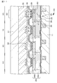
- FIG. 1 is a schematic partial cross-sectional view of a panel constituting the light emitting element of the first embodiment and the projection type display device of the first embodiment.
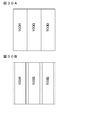
- 2A and 2B are a schematic plan view of a light emitting unit having a plurality of light emitting regions in one light emitting element and a schematic plan view of a light emitting unit having a plurality of microlens members, respectively, in the first embodiment.
- 3A and 3B are a schematic plan view of a light emitting unit having a plurality of light emitting regions in one light emitting element and a light emitting unit having a plurality of microlens members, respectively, in the modified example 1 of the first embodiment. It is a schematic plan view of.
- 4A and 4B are a schematic plan view of a light emitting unit having a plurality of light emitting regions in one light emitting element and a light emitting unit having a plurality of microlens members, respectively, in the modified example 2 of the first embodiment.
- 5A and 5B are a schematic plan view of a light emitting unit having a plurality of light emitting regions in one light emitting element and a light emitting unit having a plurality of microlens members, respectively, in the modified example 3 of the first embodiment.
- FIG. 6A and 6B are a schematic plan view of a light emitting unit having a plurality of light emitting regions in one light emitting element and a light emitting unit having a plurality of microlens members, respectively, in the modified example 4 of the first embodiment.
- It is a schematic plan view of. 7A and 7B are diagrams showing a schematic arrangement of four panels constituting the projection type display device of the first embodiment.
- FIG. 8 is a diagram schematically showing an image projection state of the four panels constituting the projection type display device of the first embodiment shown in FIG. 7A.
- FIG. 9 is a diagram schematically showing an image projection state of the four panels constituting the projection type display device of the first embodiment shown in FIG. 7B.
- FIG. 10 is a schematic partial cross-sectional view of a modified example -5 of a panel constituting the light emitting element of the first embodiment and the projection type display device of the first embodiment.
- FIG. 11 is a schematic partial cross-sectional view of a modified example -6 of a panel constituting the light emitting element of the first embodiment and the projection type display device of the first embodiment.
- FIG. 12 is a schematic partial cross-sectional view of a modified example -7 of a panel constituting the light emitting element of the first embodiment and the projection type display device of the first embodiment.
- FIG. 13 is a plan view schematically showing a metal thin film filter layer in a panel constituting the light emitting element of the first embodiment and the projection type display device of the first embodiment shown in FIG. FIG.
- FIG. 14 is a schematic partial cross-sectional view of a modified example -8 of a panel constituting the light emitting element of the first embodiment and the projection type display device of the first embodiment.
- FIG. 15 is a conceptual diagram of a modified example -9 of a panel constituting the projection type display device of the first embodiment.
- 16A and 16B are conceptual diagrams of a modified example-10 of the panel constituting the projection type display device of the first embodiment.
- FIG. 17 is a schematic partial cross-sectional view of a modified example -11 of a panel constituting the light emitting element of the first embodiment and the projection type display device of the first embodiment.
- FIG. 18 is a schematic partial cross-sectional view of a modified example -12 of a panel constituting the light emitting element of the first embodiment and the projection type display device of the first embodiment.
- FIG. 19 is a diagram schematically showing a state in which light is emitted from the light emitting element.
- 20A and 20B are schematic partial cross-sectional views of the light emitting elements of the first and fifth embodiments, respectively.
- 21A and 21B are a schematic plan view of a light emitting unit having one light emitting region in one light emitting element and a schematic plan view of the light emitting unit having a plurality of microlens members, respectively, in the second embodiment. It is a figure.
- 22A and 22B are a schematic plan view of a light emitting unit having a plurality of light emitting regions in one light emitting element and a schematic plan view of the light emitting unit having one microlens member, respectively, in the third embodiment. It is a figure. 23A and 23B are schematic plan views of a light emitting unit having a plurality of light emitting regions in one light emitting element and a light emitting unit having three microlens members, respectively, in the modified example-1 of the third embodiment. It is a schematic plan view of.
- FIG. 24 is a schematic partial cross-sectional view of one light emitting unit in the panel constituting the light emitting element of the fourth embodiment and the projection type display device of the fourth embodiment.
- FIG. 24 is a schematic partial cross-sectional view of one light emitting unit in the panel constituting the light emitting element of the fourth embodiment and the projection type display device of the fourth embodiment.
- FIG. 25 is a schematic partial cross-sectional view of one light emitting unit in the panel constituting the light emitting element of the fourth embodiment and the modified example-1 of the projection type display device of the fourth embodiment.
- FIG. 26 is a schematic partial cross-sectional view of one light emitting unit in the panel constituting the light emitting element of the fourth embodiment and the modified example-2 of the projection type display device of the fourth embodiment.
- FIG. 27 is a schematic partial cross-sectional view of a panel constituting the light emitting element of the fifth embodiment and the projection type display device of the fifth embodiment.
- 28A, 28B and 28C are schematic views for explaining the relationship between the light emitting region and the planar shape of the microlens member.
- 29A, 29B, 29C and 29D are schematic views for explaining the brightness and the like obtained when a lens having a low F value and a lens having a high F value are used.
- 30A and 30B are a schematic layout diagram of three organic electroluminescence elements constituting one pixel of a conventional organic electroluminescence display device and a schematic layout diagram of a light emitting region, respectively.
- Example 1 (light emitting element according to the first aspect of the present disclosure, a light emitting element of the first form, and a display device of the present disclosure). 3. 3.
- Example 2 (light emitting device according to the second aspect of the present disclosure) 4.
- Example 3 (light emitting device according to the third aspect of the present disclosure) 5.
- Example 4 (light emitting device according to the fourth aspect of the present disclosure) 6.
- Example 5 (light emitting element of the second embodiment) 7.
- Example 6 Combination of the light emitting element of the first form and the light emitting element of the second form) 8.
- the light emitting element according to the second aspect of the present disclosure the light emitting element according to the second aspect of the present disclosure provided in the display device of the present disclosure, and the second aspect of the present disclosure provided in the surface light emitting device of the present disclosure.
- the light emitting elements according to the second aspect of the present disclosure may be generically referred to as "light emitting elements and the like according to the second aspect of the present disclosure".
- the light emitting elements according to the third aspect may be generically referred to as "light emitting elements and the like according to the third aspect of the present disclosure". Further, the light emitting element according to the fourth aspect of the present disclosure, the light emitting element according to the fourth aspect of the present disclosure provided in the display device of the present disclosure, and the fourth of the present disclosure provided in the surface light emitting device of the present disclosure. The light emitting elements according to the fourth aspect of the present disclosure may be collectively referred to as "light emitting elements and the like according to the fourth aspect of the present disclosure".
- the light emitting element and the like according to the first aspect of the present disclosure may be generically referred to as "the light emitting elements and the like of the present disclosure”.
- a light emitting unit having a plurality of light emitting regions and one or a plurality of microlens members for controlling the traveling direction of light emitted from each light emitting region.
- the plurality of light emitting regions may be arranged at desired positions and may be regularly arranged (specifically, for example, the centers of the light emitting regions are arranged on the grid points of the virtual lattice. It does not have to be regularly arranged.
- the optical axes of the microlens member need only be arranged at a desired position and are regularly arranged. It may be (specifically, for example, the optical axis of the microlens member may be arranged on the lattice point of the virtual lattice), or it may not be regularly arranged.
- the size and shape of the light emitting region in the light emitting unit may be changed depending on the arrangement position of the light emitting unit in the display device or the surface light emitting device, or may be constant.
- the size and shape of the plurality of microlens members, various physical properties such as radius of curvature and optical power, and constituent materials may be changed depending on the arrangement position in the light emitting portion, or may be constant.
- the virtual grid may be, but is not limited to, a square grid, a rectangular grid, or a regular hexagonal grid. The same applies to the following.
- the light emitting element or the like according to the second aspect of the present disclosure includes a plurality of microlens members that control the traveling direction of light emitted from one light emitting region. For example, the light emitted from one light emitting region is emitted.
- the plurality of microlens members may be arranged at desired positions and may be regularly arranged (specifically, for example, the optical axes of the microlens members are arranged on the grid points of a virtual lattice. It does not have to be regularly arranged.
- the size and shape of the plurality of microlens members, various physical properties such as radius of curvature and optical power, and constituent materials may be changed depending on the arrangement position in the light emitting portion, or may be constant.
- the light emitting unit has a plurality of light emitting regions, and one or a plurality of microlens members that control the traveling direction of the light emitted from the plurality of light emitting regions are provided.
- the microlens member that controls the traveling direction of the light emitted from the M ⁇ N light emitting regions may be one or a plurality, for example, a plurality of microlens members.
- the plurality of light emitting regions may be arranged at desired positions and may be regularly arranged (specifically, for example, the centers of the light emitting regions are arranged on the grid points of the virtual lattice. It does not have to be regularly arranged.
- the plurality of microlens members may be arranged at desired positions and may be regularly arranged (specifically, for example, the optical axes of the microlens members are arranged on the grid points of a virtual lattice. It does not have to be regularly arranged.
- the size and shape of the light emitting region in the light emitting unit may be changed depending on the arrangement position of the light emitting unit in the display device or the surface light emitting device, or may be constant.
- the size and shape of the plurality of microlens members, various physical properties such as radius of curvature and optical power, and constituent materials may be changed depending on the arrangement position in the light emitting portion, or may be constant.
- the light emitting unit has a plurality of light emitting regions, and is provided with a light guide unit that controls the traveling direction of the light emitted from each light emitting region.
- the light guide unit that controls the traveling direction of the light emitted from the region may be one or a plurality.
- the plurality of light emitting regions may be arranged at desired positions and may be regularly arranged (specifically, for example, the centers of the light emitting regions are arranged on the grid points of the virtual lattice. It does not have to be regularly arranged.
- the plurality of light guides may be arranged at desired positions and may be regularly arranged (specifically, for example, the axes of the light guides are arranged on the grid points of a virtual lattice. It does not have to be regularly arranged.
- the size and shape of the light emitting region in the light emitting unit may be changed depending on the arrangement position of the light emitting unit in the display device or the surface light emitting device, or may be constant.
- Various physical properties such as the size and shape of the plurality of light guide portions and the constituent materials may be changed depending on the arrangement position in the light emitting portion, or may be constant.
- the light emitting element or the like according to the first to third aspects of the present disclosure includes a microlens member (lens member, on-chip lens), the light emitted from the light emitting region of the light emitting element can be emitted. , Parallel light, etc. can be set to a desired state. Further, since the light emitting element or the like according to the fourth aspect of the present disclosure includes a light guide unit (light reflecting unit, reflector unit), the light emitted from the light emitting region of the light emitting element can be converted into parallel light or the like. It can be in a desired state.
- the optical axis of the microlens member may be in a form not located on the center line passing through the center of the light emitting region.
- the light emitting element or the like according to the first aspect of the present disclosure includes a form in which the optical axis of the microlens member is located on the center line passing through the center of the light emitting region.
- the plurality of light emitting regions are regularly arranged (specifically, for example, the centers of the light emitting regions are arranged on the grid points of a virtual lattice), and the microlens member.
- the optical axis of is not located on this grid point, or the plurality of light emitting regions are not regularly arranged (specifically, for example, the center of the light emitting region is a virtual grid.
- the optical axis of the microlens member can be in a form located on this lattice point, or can be a combination of these forms.
- the planar shape of the microlens member may be a rectangle or a square having rounded corners.
- examples of the planar shape of the light emitting region include a rectangle, a square, a polygon, a rectangle or a square with rounded corners, and a polygon, a circle, and an ellipse with rounded corners. ..
- the microlens member is a spherical lens or an aspherical lens.
- the microlens member may have a convex surface toward a direction away from the light emitting region, or may have a convex surface toward the light emitting region. It may have a surface of.
- the optical axis of the microlens member is located on the center line passing through the center of the light emitting region. If so, the orthophoto image in the light emitting region can be in a form included in the orthophoto image of the microlens member. Specifically, in the light emitting element or the like according to the first aspect of the present disclosure, when the optical axis of the microlens member is located on the center line passing through the center of the light emitting region, a normal projection image of one light emitting region is obtained. Can be included in the orthophoto image of one microlens member.
- the orthophoto image of one light emitting region is P.
- the number of microlens members x Q can be included in the entire orthophoto image.
- M ⁇ N positive light emitting regions are positive.
- the projected image can be in a form included in the normal projected image of one microlens member.
- the second microlens member that controls the traveling direction of the light emitted from the microlens member can be further provided.
- the light emitting element or the like according to the first to third aspects of the present disclosure including the preferred embodiment described above further includes a light guide unit that controls the traveling direction of the light emitted from the microlens member. It can be in the form.
- the inner surface of the light guide section (the surface of the light guide section where the light emitted from the microlens member collides) when cut in a virtual plane orthogonal to the normal direction of the light emitting region is parallel to the normal direction of the light emitting region. It may be present or it may be non-parallel.
- the inner surface of the light guide portion may have a forward taper shape or a reverse taper shape when the light emitting region is used as a reference, but from the viewpoint of light collection, the inner surface has a reverse taper shape. Is preferable. Further, in this case, it has a structure in which a plurality of light guide portions are laminated; the axes of the plurality of light guide portions may be in a form that is not in the same linear shape. Of course, the axes of the plurality of light guides may be in the same linear shape. Further, the axis at the bottom of the light guide portion closest to the light emitting region may be in a form not located on the center line passing through the center of the light emitting region.
- the form in which the axis at the bottom of the light guide portion closest to the light emitting region is located on the center line passing through the center of the light emitting region is included. Further, when the axis at the bottom of the light guide portion closest to the light emitting region is located on the center line passing through the center of the light emitting region, the orthophoto image of the light emitting region is within the orthophoto image of the bottom of the light emitting region. It can be in the form included. The above description can be applied to a light emitting device or the like according to the fourth aspect of the present disclosure.
- the fact that the inner surface of the light guide portion has a forward taper shape means a shape in which the inner surface of the light guide portion expands (a shape that expands toward the second substrate) as the distance from the light emitting region increases.
- the fact that the inner surface has an inverted taper shape means a shape in which the inner surface of the light guide portion expands and narrows (a shape that narrows toward the second substrate) as the distance from the light emitting region increases.
- the light emitting part The first electrode shared in the light emitting region, An organic layer formed on the first electrode and including a light emitting layer made of an organic light emitting material, and A second electrode formed on the organic layer, Is equipped with Further, a light reflecting layer is provided below the first electrode. The light emitted by the light emitting layer is resonated between the interface between the second electrode and the organic layer and the light reflecting layer, and a part of the light is emitted from the second electrode.
- An insulating layer is formed between the first electrode and the organic layer. The insulating layer may be provided with an opening that defines a light emitting region.
- the light emitting element of such a form may be referred to as a "light emitting element of the first form" for convenience.
- first interface the interface between the second electrode and the organic layer
- second interface the first interface and the second interface are referred to.
- a resonator structure is formed with the interface.
- the light emitting part The first electrode shared in the light emitting region, An organic layer formed on the first electrode and including a light emitting layer made of an organic light emitting material, and A second electrode formed on the organic layer, Is equipped with The light emitting layer is formed by stacking a plurality of light emitting layers that emit light of the same color.
- An insulating layer is formed between the first electrode and the organic layer.
- the insulating layer may be provided with an opening that defines a light emitting region.
- the plurality of light emitting layers can have the same composition.
- such a light emitting element may be referred to as a "second type light emitting element".
- the microlens member can be configured to have a positive optical power.
- the light emitting region has a configuration having a convex shape in the direction away from the microlens member. can do.
- the microlens member can be configured to have a negative optical power.
- the light emitting region can be in a form having positive optical power, and further described above.
- the light emitting element or the like according to the fourth aspect of the present disclosure including the preferred embodiment and configuration has a structure in which a plurality of light guide portions are laminated; the axes of the plurality of light guide portions have the same linear shape. It can be in a form not found in. Of course, a form in which the axes of the plurality of light guides are in the same straight line is also included.
- the display device can be in the form of a projection type display device.
- the microlens member can be made of, for example, a transparent resin material such as an acrylic resin, and can be obtained by melt-flowing the transparent resin material or by etching back. However, it can also be obtained by a method such as forming a transparent resin material into a lens shape based on the nanoprint method.
- a transparent resin material such as an acrylic resin
- the light guide portion may be composed of a material that reflects light emitted from a light emitting region or a microlens member, and for example, light emitted from a metal material, an alloy material, a light emitting region, or a microlens member.
- a metal material for example, Al—Nd layer
- a chromium (Cr) layer for example, a silver (Ag) layer
- a silver alloy layer for example,).
- Ag-Cu layer, Ag-Pd-Cu layer, Ag-Sm-Cu layer can be mentioned, for example, an electron beam vapor deposition method, a hot filament vapor deposition method, a vapor deposition method including a vacuum vapor deposition method, a sputtering method, and a CVD method. And ion plating method; plating method (electroplating method or electroless plating method); lift-off method; laser ablation method; sol-gel method or the like.
- the value of the full width at half maximum (FWHM) of the light emitted from the light emitting element can be 30 nm or less.
- the value of the full width at half maximum (FWHM) of the light emitted from the conventional organic EL element described later is often 60 nm to 100 nm, and the light emitting element and the like of the present disclosure have a sharper emission spectrum than the conventional organic EL element. ..
- the light intensity (light intensity of the light emitted from the light emitting element) at the center line passing through the center of the light emitting portion of the light emitting element is defined as I 0 .
- the light intensity (light intensity of light emitted from the light emitting element) at the center line passing through the center of the light emitting part of the light emitting element having no light reflecting layer is I conv .
- I 0 / I conv ⁇ 5 Can be made into a satisfying form.
- the light intensity (light intensity of the light emitted from the light emitting portion) at the center line passing through the center of the light emitting portion of the light emitting element is set to 100%.
- the direction with respect to the center line, which has a light intensity of 50% (the light intensity of the light emitted from the light emitting portion), and the directional half-value angle, which is the angle formed by the center line may be 25 degrees or less. it can.
- the half-pointed angle of Lambersian radiation is about 70 degrees.
- the light emitted from the light emitting element or the like of the present disclosure is light having higher directivity than the conventional organic EL element described later, or light close to parallel light. Therefore, the telecentric optical system that is often required between the light source of the conventional projection type display device (projector) and the spatial modulator is unnecessary, and the projection type display device can be simplified. Further, since the light emitted from the light emitting element or the like of the present disclosure is highly directional light or light close to parallel light, the light generated by the light emitting layer is the first substrate and the second light. It is possible to prevent the occurrence of a phenomenon in which total reflection is repeated between the substrate and the light emitted from the joint portion (end face of the panel) of the first substrate and the second substrate, and the light emitted from the panel is lost. ..
- the optical distance from the maximum light emitting position of the light emitting layer to the first interface is OL 1
- the maximum light emitting of the light emitting layer is OL 2
- the configuration can satisfy the following equations (1-1) and (1-2).
- ⁇ Maximum peak wavelength of the spectrum of light generated in the light emitting layer (or desired wavelength in the light generated in the light emitting layer)
- ⁇ 1 The amount of phase shift (unit: radian) of the reflected light (light reflected at the first interface) generated at the first interface.
- -2 ⁇ ⁇ 1 ⁇ 0 ⁇ 2 The amount of phase shift (unit: radian) of the reflected light (light reflected at the second interface) generated at the second interface.
- the value of m 1 is larger than or equal to zero, the value of m 2 is independently a value of m 1, is a value of 0 or more, to satisfy the m 1 ⁇ 1, m 2 ⁇ 1, It is preferable from the viewpoint of potential design in the organic layer, that is, from the viewpoint of optimizing the potential in the organic layer, and as will be described later, it is possible to reduce the value of the half-value full width (FWHM) of the light emitted from the light emitting element. it can.
- FWHM half-value full width
- the distance L 1 from the maximum light emitting position of the light emitting layer to the first interface refers to the actual distance (physical distance) from the maximum light emitting position of the light emitting layer to the first interface, and is the second from the maximum light emitting position of the light emitting layer.
- the distance L 2 to the interface refers to the actual distance (physical distance) from the maximum light emitting position of the light emitting layer to the second interface.
- the optical distance is also called an optical path length, and generally refers to n ⁇ L when a light ray passes through a medium having a refractive index n by a distance L. The same applies to the following.
- the desired wavelength ⁇ (specifically, the red wavelength, the green wavelength, and the blue wavelength) of the light generated in the light emitting layer is determined, and based on the equations (1-1) and (1-2).
- the light emitting element may be designed by obtaining various parameters such as OL 1 and OL 2 in the light emitting element.
- the light reflecting layer and the second electrode absorb a part of the incident light and reflect the rest. Therefore, a phase shift occurs in the reflected light.
- the phase shift amounts ⁇ 1 and ⁇ 2 are calculated by measuring the values of the real and imaginary parts of the complex refractive index of the materials constituting the light reflecting layer and the second electrode using, for example, an ellipsometer. (See, for example, "Principles of Optic", Max Born and Emil Wolf, 1974 (PERGAMON PRESS)).
- An ellipsometer is used to determine the refractive index of the first electrode, such as an organic layer or an interlayer insulating layer, or the refractive index of the first electrode when the first electrode absorbs a part of the incident light and reflects the rest. It can be obtained by measuring.
- aluminum As a material constituting the light reflecting layer, aluminum, aluminum alloy (for example, Al—Nd or Al—Cu), Al / Ti laminated structure, Al—Cu / Ti laminated structure, chromium (Cr), silver (Ag), silver.
- alloys for example, Ag-Cu, Ag-Pd-Cu, Ag-Sm-Cu.
- Ablation method It can be formed by a sol-gel method or the like.
- a base film made of, for example, TiN in order to control the crystal state of the light-reflecting layer to be formed.
- a light absorption layer (black matrix layer) is formed between the microlens member or the light guide portion of the adjacent light emitting element. It can be in the form.
- a light absorption layer black matrix layer
- the light absorbing layer is made of, for example, a black resin film (specifically, for example, a black polyimide resin) having an optical density of 1 or more mixed with a black colorant, or also utilizes the interference of a thin film. It is composed of a thin film filter.
- the thin film filter is formed by stacking two or more thin films made of, for example, a metal, a metal nitride or a metal oxide, and attenuates light by utilizing the interference of the thin films.
- Specific examples of the thin film filter include those in which Cr and chromium (III) oxide (Cr 2 O 3 ) are alternately laminated.
- the first electrode and the light reflecting layer can be in a form surrounded by a light-shielding portion. That is, a light-shielding portion may be provided between the light-emitting element and the light-emitting element.
- a light-shielding portion may be provided between the light-emitting element and the light-emitting element.
- the light-shielding material constituting the light-shielding portion light such as titanium (Ti), chromium (Cr), tungsten (W), tantalum (Ta), aluminum (Al), and MoSi 2 can be shielded. Materials can be mentioned.
- the light-shielding portion can be formed by an electron beam vapor deposition method, a hot filament vapor deposition method, a vapor deposition method including a vacuum vapor deposition method, a sputtering method, a CVD method, an ion plating method, or the like.
- a metal thin film filter layer may be further formed between the first electrode and the light reflecting layer. It can.
- the metal thin film filter layer is made of, for example, gold (Au), silver (Ag), platinum (Pt), aluminum (Al), copper (Cu), tungsten (W), or an alloy containing these materials, for example.
- a large number of holes having a planar shape of about 200 nm and having a planar shape such as a circle, an ellipse, a rectangle, a "U", and a cross are formed and arranged in a two-dimensional shape (for example, a lattice).
- the metal thin film filter layer is disclosed in, for example, Japanese Patent Application Laid-Open No. 2015-232599.
- SPR surface plasmon polariton
- the metal thin film filter layer subjected to such periodic microfabrication is also called a plasmonic filter (hole array filter).
- the metal thin film filter layer is widely known in the field of an imaging device, its use in a projection display device provided with a self-luminous type light emitting element is not known as far as the present inventor has investigated.
- the metal thin film filter layer described above is formed instead of the light reflecting layer, and the light is emitted by the metal thin film filter layer. It may be reflected.
- the second electrode When the second electrode functions as a cathode electrode as a material (semi-light transmitting material or light transmitting material) constituting the second electrode, it transmits emitted light and efficiently transmits electrons to the organic layer (light emitting layer). It is desirable to construct it from a conductive material having a small work function value so that it can be injected in a positive manner, and it is selected from the group consisting of Ag, Ag-Mg, Ag-Nd-Cu, Ag-Cu, Au, Al and Al-Cu. It can be in the form of at least one material.
- an alloy of aluminum (Al), silver (Ag), magnesium (Mg), calcium (Ca), sodium (Na), strontium (Sr), alkali metal or alkaline earth metal and silver (Ag)
- an alloy of magnesium (Mg) and silver (Ag) (Mg-Ag alloy)] an alloy of magnesium-calcium (Mg-Ca alloy), an alloy of aluminum (Al) and lithium (Li) (Al-Li alloy)
- the second electrode when the second electrode functions as an anode electrode, it is desirable that the second electrode is made of a conductive material that transmits emitted light and has a large work function value.
- the thickness of the second electrode 4 nm to 50 nm, preferably 4 nm to 20 nm, and more preferably 6 nm to 12 nm can be exemplified.
- the average light transmittance of the second electrode is preferably 50% to 90%, preferably 60% to 90%.
- the first electrode when transparency is not required for the first electrode, when the first electrode functions as an anode electrode as a material constituting the first electrode, for example, platinum (Pt), gold (Au), silver (Ag), etc.
- Metals or alloys with high work functions such as chromium (Cr), tungsten (W), nickel (Ni), copper (Cu), iron (Fe), cobalt (Co), and tantalum (Ta) (for example, silver is the main component).
- Ag-Pd-Cu alloy containing 0.3% by mass to 1% by mass of palladium (Pd) and 0.3% by mass to 1% by mass of copper (Cu), Al-Nd alloy, Al-Cu alloy. , Al—Cu—Ni alloy).
- a conductive material having a small work function value such as aluminum (Al) and an alloy containing aluminum and having a high light reflectance is used, hole injection is performed by providing an appropriate hole injection layer. By improving the characteristics, it can be used as an anode electrode.
- As the thickness of the first electrode 0.1 ⁇ m to 1 ⁇ m can be exemplified.
- ITO indium and tin
- ITO oxide of indium and zinc
- a highly light-reflecting reflective film such as a dielectric multilayer film or aluminum (Al) or an alloy thereof (for example, Al—Cu
- indium-tin oxide (including ITO, Indium Tin Oxide, Sn-doped In 2 O 3 , crystalline ITO and amorphous ITO) is used as a material for forming the first electrode.
- Indium-zinc oxide IZO, Indium Zinc Oxide
- IGO indium-gallium oxide
- IGZO indium-doped gallium-zinc oxide
- IFO IFO
- F Dope In 2 O 3
- ITOO Ti Dope In 2 O 3
- Zinc Oxide ZnO), aluminum oxide-doped zinc oxide (AZO), gallium-doped zinc oxide (GZO), B-doped ZnO, AlMgZnO (aluminum oxide and magnesium oxide-
- Examples of the method for forming the first electrode and the second electrode include an electron beam deposition method, a hot filament deposition method, a vapor deposition method including a vacuum vapor deposition method, a sputtering method, a chemical vapor deposition method (CVD method), a MOCVD method, and an ion.
- Combination of plating method and etching method; various printing methods such as screen printing method, inkjet printing method, metal mask printing method; plating method (electroplating method and electroless plating method); lift-off method; laser ablation method; sol gel The law etc. can be mentioned. According to various printing methods and plating methods, it is possible to directly form the first electrode and the second electrode having a desired shape (pattern).
- the second electrode is formed after the organic layer is formed, it can be formed based on a film forming method such as a vacuum vapor deposition method in which the energy of the formed particles is small, or a film forming method such as a MOCVD method. , It is preferable from the viewpoint of preventing the occurrence of damage to the organic layer.
- a film forming method such as a vacuum vapor deposition method in which the energy of the formed particles is small
- a film forming method such as a MOCVD method.
- an intermediate layer (charge generation layer) may be formed between the light emitting layer and the light emitting layer.
- materials constituting the intermediate layer lithium (Li), calcium (Ca), sodium (Na), cesium (Cs), molybdenum oxide (MoO 3 ), vanadium oxide (V 2 O 5 ) and tungsten oxide ( At least one material selected from the group consisting of WO 3 ) can be mentioned, and broadly, conductive metal materials, alloy materials, and metal compounds can be mentioned. It is necessary to prevent damage to the light emitting layer due to the film formation of the intermediate layer.
- the intermediate layer is formed on a light emitting layer made of an organic material by, for example, a sputtering method, but if the film forming temperature of the intermediate layer exceeds, for example, 100 ° C, the light emitting layer may be damaged. There is. Therefore, when the intermediate layer is formed based on the sputtering method, the material constituting the intermediate layer needs to be selected from the materials whose film forming temperature can be 100 ° C. or less.
- the thickness of the intermediate layer may be, but is not limited to, 2 nm to 10 nm.
- the light emitting element of the second form has a light reflecting layer,
- the light emitted by the light emitting layer may be resonated between the second interface between the second electrode and the organic layer and the light reflecting layer, and a part of the light may be emitted from the second electrode.
- the light reflecting layer may be arranged below the first electrode, or may be arranged above the first electrode and below the light emitting layer. .. It should be noted that such a preferable configuration of the light emitting element of the second form can include the light emitting element of the first form described above, but in this case, a light emitting layer formed by stacking a plurality of light emitting layers that emit light of the same color.
- the maximum light emitting position of the light emitting layer in the above indicates the position in the average thickness direction of the plurality of light emitting layers. Specifically, the position corresponding to the average value of the distances between the interface between the first electrode and the organic layer (first interface) and the center of each light emitting layer in the thickness direction is defined as the maximum light emitting position.
- the first electrode is not necessarily required to be transparent. Further, in some cases, the formation of the light reflecting layer may be omitted so that the first electrode also serves as the light reflecting layer. In this case, the distance from the maximum light emitting position of the light emitting layer to the first electrode is L. 1. Let the optical distance be OL 1, and let the phase shift amount of the reflected light (light reflected by the light reflecting layer) generated at the first electrode be ⁇ 1 .
- the number of light emitting layers (NL) is 2 or more, but is not limited, but "4" can be exemplified as the upper limit value.
- the number of layers in the intermediate layer is (NL-1).
- the number of layers NL of the light emitting layer increases, the voltage for driving the light emitting element increases. Therefore, the number of layers NL of the light emitting layer is the voltage for driving the light emitting element, and further, the voltage for driving the light emitting element. Limited by pressure resistance.
- the panel is a monochromatic light [for example, red light (having an emission spectrum peak in the wavelength range of 620 nm to 750 nm). , Green light (wavelength: having an emission spectrum peak in the range of 495 nm to 570 nm), blue light (having an emission spectrum peak in the wavelength range of 450 nm to 495 nm)] is emitted.
- red light having an emission spectrum peak in the wavelength range of 620 nm to 750 nm.
- Green light wavelength: having an emission spectrum peak in the range of 495 nm to 570 nm
- blue light having an emission spectrum peak in the wavelength range of 450 nm to 495 nm
- the display device of the present disclosure (for example, a projection type display device) is One red light emitting panel that emits red light, One green light emitting panel that emits green light, and
- the form may be composed of three panels of one blue light emitting panel that emits blue light. Further, in this case, it is possible to further have one blue light emitting panel for emitting blue light or one green light emitting panel for emitting green light, and to form a form composed of four panels. it can. In this case, the four panels may be arranged in an array (1 ⁇ 4 state), or the four panels may be arranged in a 2 ⁇ 2 state. You can also do it.
- the display device of the present disclosure including the above-mentioned preferable form and configuration, specifically, the projection type display device may be further provided with a projection lens system on the light emitting side.
- An image compositing means for example, an unpolarized dichroic prism or a Philips prism
- the image synthesizing means may be provided with a projection lens system on the light emitting side.
- three panels or four panels constituting the projection display device may be provided. The panels may be arranged at the optimum positions in the image compositing means.
- the light incident on the projection lens system or the image synthesizing means is preferably parallel light with respect to the optical axis of the lens in the paraxial region of the lens.
- a microlens member is provided on the light emitting side of the light emitting element.
- a light guide portion is provided, and for example, the resonator structure is optimized.
- the panel can be not only in a flat form but also in a curved form.
- a projection type display device does not have means for synthesizing images emitted from a plurality of panels into one image, a plurality of display devices.
- the image formed on the screen is trapezoidal correction, distortion correction, magnification correction, etc. at the same time as performing appropriate alignment of a plurality of panels.
- Various corrections may be made using software.
- the pixels of the images from the plurality of panels may not be completely overlapped but may be partially overlapped. .. As long as it is below the resolution limit of the observer's eyes, there is no problem even if the pixels are displaced.
- the light emitting unit constituting the light emitting element can be in a form including an organic electroluminescence layer. That is, the panel and the surface light emitting device constituting the display device (for example, the projection type display device) of the present disclosure including the various preferable forms and configurations described above are in the form of an organic electroluminescence panel (organic EL panel).
- the light emitting element can be in the form of an organic electroluminescence element (organic EL element), and the organic layer can be in the form of an organic electroluminescence layer.
- the organic EL panel can be a top emission type (top emission type) organic EL panel (top emission type organic EL panel) that emits light from the second substrate, and the light from the organic layer is emitted from the second substrate. It is emitted to the outside via.
- top emission type top emission type organic EL panel
- the light emitting portion constituting the light emitting element includes an organic electroluminescence layer and a form in which the panel is composed of a top emission type organic EL panel will be described.
- the light emitting portion of the light emitting element is composed of a first electrode, an organic layer, and a second electrode.
- the first electrode may be in contact with a part of the organic layer, or the organic layer may be in contact with a part of the first electrode.
- the size of the first electrode can be smaller than that of the organic layer, or the size of the first electrode is the same as that of the organic layer, but the first electrode and the organic layer are organic.
- An insulating layer may be formed in a part between the layers, or the size of the first electrode may be larger than that of the organic layer.
- the region where the first electrode and the organic layer are in contact with each other, and the region of the opening provided in the insulating layer is the light emitting region.
- the region where the first electrode and the organic layer are in contact with each other is a light emitting region.
- Insulating materials such as SiO 2 , SiN, and SiON can be exemplified as the material constituting the substrate.
- the substrate is formed by a forming method suitable for the material constituting the substrate, specifically, various printing methods such as various CVD methods, various coating methods, various PVD methods including sputtering method and vacuum deposition method, screen printing method, and plating. It can be formed based on known methods such as a method, an electrodeposition method, a dipping method, and a sol-gel method.
- the first substrate or the second substrate can be a silicon semiconductor substrate, a high-distortion point glass substrate, a soda glass (Na 2 O / CaO / SiO 2 ) substrate, or a borosilicate glass (Na 2 O / B 2 O 3 / SiO 2 ) substrate.
- Organic polymers such as quartz substrates, polymethylmethacrylate (polymethylmethacrylate, PMMA), polyvinyl alcohol (PVA), polyvinylphenol (PVP), polyethersulfone (PES), polyimide, polycarbonate, polyethylene terephthalate (PET) (PET). It can be composed of a flexible plastic film composed of a polymer material, a plastic sheet, a plastic substrate, or the like).
- the materials constituting the first substrate and the second substrate may be the same or different.
- the substrate that transmits the light from the light emitting element is required to be transparent to the light from the light emitting element.
- the organic layer includes a light emitting layer made of an organic light emitting material. Specifically, for example, it also serves as a laminated structure of a hole transport layer, a light emitting layer, and an electron transport layer, and a hole transport layer and an electron transport layer. It can be composed of a laminated structure with a light emitting layer, a laminated structure of a hole injection layer, a hole transport layer, a light emitting layer, an electron transport layer, an electron injection layer, and the like.
- a physical vapor deposition method such as a vacuum vapor deposition method
- a printing method such as a screen printing method or an inkjet printing method
- a lamination of a laser absorbing layer and an organic layer formed on a transfer substrate
- a laser transfer method in which the organic layer on the laser absorbing layer is separated by irradiating the structure with a laser and the organic layer is transferred, and various coating methods can be exemplified.
- a so-called metal mask is used, and the organic layer can be obtained by depositing a material that has passed through an opening provided in the metal mask.
- a protective layer (flattening layer) is formed between the second electrode and the second substrate.
- acrylic resin can be exemplified, and SiN, SiON, SiC, amorphous silicon ( ⁇ —Si), Al 2 O 3 , and TiO 2 can also be exemplified.
- a method for forming the protective layer it can be formed based on a known method such as various CVD methods, various coating methods, various PVD methods including a sputtering method and a vacuum vapor deposition method, and various printing methods such as a screen printing method. Further, as a method for forming the protective layer, an ALD (Atomic Layer Deposition) method can also be adopted.
- ALD Atomic Layer Deposition
- the protective layer may be shared by a plurality of light emitting elements, or may be individually provided in each light emitting element.
- the protective layer and the second substrate are joined via, for example, a resin layer (sealing resin layer).
- a resin layer laminated with heat-curable adhesives
- heat-curable adhesives such as acrylic adhesives, epoxy adhesives, urethane adhesives, silicon adhesives, and cyanoacrylate adhesives, and ultraviolet curable adhesives.
- Adhesives can be mentioned.
- SiO 2 In an organic EL panel, a substrate, an insulating layer, and an interlayer insulating layer are formed.
- insulating materials constituting these SiO 2 , NSG (non-doped silicate glass), BPSG (boron phosphorus silicate glass) constitutes PSG, BSG, AsSG, SbSG, PbSG, SOG ( spin on glass), LTO (low Temperature oxide, low temperature CVD-SiO 2), low-melting glass, SiO X materials such as glass paste (silicon oxide film Material); SiN-based material including SiON-based material; SiOC; SiOF; SiCN.
- SiO X materials such as glass paste (silicon oxide film Material); SiN-based material including SiON-based material; SiOC; SiOF; SiCN.
- Inorganic insulating materials such as (Nb 2 O 5 ), tin oxide (SnO 2 ), and vanadium oxide (VO x) can be mentioned.
- various printing methods such as various CVD methods, various coating methods, various PVD methods including sputtering method and vacuum vapor deposition method, screen printing method, plating method, electrodeposition method, immersion method, sol- It can be formed based on a known method such as a gel method.
- the thickness of the hole transport layer (hole supply layer) and the thickness of the electron transport layer (electron supply layer) are approximately equal.
- the electron transport layer (electron supply layer) may be thicker than the hole transport layer (hole supply layer), which is necessary for high efficiency at a low drive voltage and sufficient for the light emitting layer.
- Electronic supply is possible. That is, the hole supply can be increased by arranging the hole transport layer between the first electrode corresponding to the anode electrode and the light emitting layer and forming the hole transport layer with a film thickness thinner than that of the electron transport layer. It will be possible.
- Example 1 relates to a light emitting element according to the first aspect of the present disclosure and a display device of the present disclosure, and also relates to a light emitting element of the first embodiment.
- FIG. 1 shows a schematic partial cross-sectional view of a panel constituting the light emitting element of the first embodiment and the display device of the first embodiment (specifically, a projection type display device).
- FIG. 2A shows a schematic plan view of a light emitting unit having a light emitting region of (pieces ⁇ N pieces), and
- FIG. 2B shows a schematic plan view of a light emitting part having a plurality of (P pieces ⁇ Q pieces) microlens members. Shown.
- FIGS. 7A and 7B the schematic arrangement of the four panels constituting the projection type display device of the first embodiment is shown in FIGS. 7A and 7B, and the projection type display device of the first embodiment shown in FIGS. 7A and 7B is configured.
- the image projection state of the panel is schematically shown in FIGS. 8 and 9.
- a schematic partial cross-sectional view of the light emitting element of the first embodiment is shown in FIG. 20A.
- FIG. 2A, FIG. 3A, FIG. 4A, FIG. 5A, FIG. 6A, FIG. 21A, FIG. 22A and FIG. 23A one light emitting region is shown by a solid line
- FIG. 2B, FIG. 3B, FIG. 4B, FIG. 5B, FIG. 21B, 22B and 23B one microlens member is shown by a solid line and one light emitting region is shown by a long and short dash line.
- FIG. 2A, FIG. 2B, FIG. 3A, FIG. 3B, FIG. 4A, FIG. 4B, FIG. In 5A, FIG. 5B, FIG. 6A, FIG. 6B, FIG. 21A, FIG. 21B, FIG. 22A, FIG. 22B, FIG. 23A and FIG. Surrounded by.
- the center line passing through the center of the light emitting region is indicated by a white circle
- the optical axis of the microlens member is indicated by a black circle.
- the light emitting element 10 of the first embodiment is A light emitting unit 30 having a plurality of light emitting regions 30'and One or more microlens members 60 that control the traveling direction of the light emitted from each light emitting region 30', It has.
- (Integer) microlens member 60 It has.
- the display device of the first embodiment or the second to sixth embodiments described later specifically, the projection type display device (projector) 1st substrate 11, Second substrate 41 and A plurality of light emitting elements sandwiched between the first substrate 11 and the second substrate 41, Equipped with a panel with Each light emitting element is composed of the light emitting element 10 of Example 1 or Examples 2 to 6 described later.
- the light emitting element 10 of the first embodiment is the light emitting element of the first embodiment.
- the light emitting unit 30 The first electrode 31, shared in the light emitting region 30', An organic layer 33 formed on the first electrode 31 and including a light emitting layer 33A made of an organic light emitting material, and The second electrode 32 formed on the organic layer 33, Is equipped with Further, a light reflecting layer 50 is provided below the first electrode 31.
- the light emitted by the light emitting layer 33A is resonated between the interface between the second electrode 32 and the organic layer 33 and the light reflecting layer 50, and a part of the light is emitted from the second electrode 32.
- An insulating layer 28 is formed between the first electrode 31 and the organic layer 33.
- the insulating layer 28 is provided with an opening 29 that defines a light emitting region 30'. Then, a resonator structure is formed between the surface of the light reflecting layer 50 on the side of the first electrode 31 (first interface) and the interface between the second electrode 32 and the organic layer 33 (second interface).
- the size of one light emitting portion 30 is 7.8 ⁇ m ⁇ 7.8 ⁇ m
- the size of one opening 29 (one light emitting region 30') is 2.2 ⁇ m ⁇ 2.2 ⁇ m.
- the size of the region including one light emitting region 30' was set to 2.6 ⁇ m ⁇ 2.6 ⁇ m.
- the planar shape of one opening 29 (one light emitting region 30') is square.
- the planar shape of the microlens member 60 is a square with rounded corners, and the size is, for example, 2.2 ⁇ m ⁇ 2.2 ⁇ m.
- the microlens member 60 is larger than the opening 29 (light emitting region 30'). This is because the light emitted from the light emitting unit 30 has a divergence angle, so that the microlens member 60 that covers the divergence angle can improve the light collection efficiency.
- the microlens member 60 is a kind of aspherical lens, is composed of a plano-convex lens, and has a convex surface toward a direction away from the light emitting region 30'. In the examples shown in FIGS. 2A and 2B, the optical axis of the microlens member 60 is located on the center line passing through the center of the light emitting region 30', and the orthophoto image of the light emitting region 30'is the microlens member 60.
- the orthophoto image of one light emitting region 30' is included in the orthophoto image of one microlens member 60.
- the microlens member 60 has positive optical power.
- the plurality of light emitting regions 30's may be arranged at desired positions, and specifically, they are regularly arranged. That is, for example, the center of the light emitting region 30'is arranged on the grid points of a virtual grid (square grid).
- the size of the microlens member 160'for passing the light emitted from the light emitting region 130' is As shown in FIG. 28B, it becomes larger with respect to the light emitting region 130'.
- FIG. 28C it is difficult for the microlens member 160'to efficiently collect the light emitted in the corner region of the light emitting region 130'.
- the planar shape of the light emitting region 130' is square and the planar shape of the microlens member 160 is square
- the size of the microlens member 160 for passing the light emitted from the light emitting region 130' is As shown in FIG.
- the size is not so large, and the microlens member 160 can efficiently collect the light emitted in the corner region of the light emitting region 130'.
- the planar shape of the light emitting region 130' is square and the planar shape of the microlens member 160 is square, the area occupied by the microlens member 160 can be reduced, and the light emitting region 130'can be reduced. The light from the lens can be efficiently collected.
- the panel constituting the projection type display device is composed of an organic EL panel
- the light emitting element 10 is composed of an organic EL element
- the organic layer 33 is composed of an organic electroluminescence layer.
- the organic EL panel is a top emission type organic EL panel that emits light from the second substrate 41, and the light from the organic layer 33 is emitted to the outside via the second substrate 41.
- the projection type display device of the first embodiment or the second to sixth embodiments described later is One red light emitting panel (first panel 1R) that emits red light, One green light emitting panel (second panel 1G) that emits green light, and It is composed of one blue light emitting panel (third panel 1B 1) that emits blue light, and further has one blue light emitting panel (fourth panel 1B 2 ) that emits blue light. However, it is composed of four panels 1R, 1G, 1B 1 , and 1B 2.
- a projection lens system 70 is provided on the light emitting side of the projection type display device. As shown in FIGS. 7A and 8, the four panels may be arranged in an array (1 ⁇ 4 state), or as shown in FIGS.
- the four panels may be 2 ⁇ . It may be arranged in the state of 2.
- the light rays emitted from the panel are indicated by dotted lines and alternate long and short dash lines.
- the number of pixels of the panel is, for example, 1920 ⁇ 1080, and one light emitting element 10 constitutes one pixel.
- the size of the panel is, for example, 10 mm ⁇ 10 mm.
- the light emitting layer in the light emitting element constituting the first panel 1R is composed of a red light light emitting layer that emits red light, and the light emitted by the first panel 1R has an emission spectrum peak within the range of red light (wavelength: 620 nm to 750 nm). Specifically, the peak wavelength ⁇ R is as shown in Table 1 below. Further, the light emitting layer in the light emitting element constituting the second panel 1G is composed of a green light light emitting layer that emits green light, and the light emitted by the second panel 1G is green light (wavelength: emission spectrum within the range of 495 nm to 570 nm).
- the peak wavelength ⁇ G is as shown in Table 1 below.
- the light emitting layer in the light emitting elements constituting the third panel 1B 1 and the fourth panel 1B 2 is composed of a blue light emitting layer that emits blue light, and the light emitted by the third panel 1B 1 and the fourth panel 1B 2 is , Blue light (wavelength: having an emission spectrum peak in the range of 450 nm to 495 nm), and the peak wavelength ⁇ B is as shown in Table 1 below.
- the values of the optical distances (OL 1 + OL 2 ) obtained from the equations (1-1) and (1-2) are shown in Table 1 below.
- the second electrode 32 is covered with a protective layer (flattening layer) 34 made of an acrylic resin.
- a microlens member 60 is arranged on the light emitting side of the organic layer 33. That is, a microlens member 60 made of a well-known material is formed on the protective layer 34 by a well-known method. The light emitted from the microlens member 60 is regarded as parallel light (telecentric light).
- the protective layer 34 and the microlens member 60 are attached to the second substrate 41 via the sealing resin layer 35.
- a heat-curable adhesive such as an acrylic adhesive, an epoxy adhesive, a urethane adhesive, a silicon adhesive, or a cyanoacrylate adhesive, or an ultraviolet curable adhesive is used. Can be mentioned.
- a light reflecting layer 50 made of Al—Cu, Ag, and Ag—Cu is formed inside the substrate (interlayer insulating layer) 26 made of SiO 2 formed by the CVD method. That is, the substrate (interlayer insulating layer) 26 is composed of two layers, a lower interlayer insulating layer 26A and an upper interlayer insulating layer 26B, and the light reflecting layer 50 is located between the lower interlayer insulating layer 26A and the upper interlayer insulating layer 26B. It is formed.
- the light reflecting layer 50 is made of silver (Ag), for example, a base film made of TiN is formed on the lower interlayer insulating layer 26A in order to control the crystal state of the light reflecting layer 50 to be formed. It is preferable to keep it.
- the lower interlayer insulating layer and the upper interlayer insulating layer may be made of the same material, or may be made of different materials in order to set OL 1 to an appropriate value.
- the light emitting element driving unit is provided below the substrate (interlayer insulating layer) 26.
- the light emitting element drive unit may have a well-known circuit configuration.
- the light emitting element driving unit is composed of a transistor (specifically, a MOSFET) formed on a silicon semiconductor substrate corresponding to the first substrate 11.
- the transistor 20 composed of the MOSFET includes a gate insulating layer 22 formed on the first substrate 11, a gate electrode 21 formed on the gate insulating layer 22, a source / drain region 24 formed on the first substrate 11, and a source /. It is composed of a channel forming region 23 formed between the drain regions 24, and an element separation region 25 surrounding the channel forming region 23 and the source / drain region 24.
- the transistor 20 and the first electrode 31 are electrically connected to each other via a contact plug 27 provided on the substrate 26.
- one transistor 20 is shown for each light emitting element drive unit.
- the second electrode 32 is connected to the light emitting element driving unit via a contact hole (contact plug) (not shown) formed in the substrate (interlayer insulating layer) 26 on the outer peripheral portion of the organic EL panel.
- a contact hole contact plug
- an auxiliary electrode connected to the second electrode 32 may be provided below the second electrode 32, and the auxiliary electrode may be connected to the light emitting element driving unit.
- the organic layer 33 is, for example, a hole injection layer (HIL: Hole Injection Layer), a hole transport layer (HTL: Hole Transport Layer), a light emitting layer 33A, and an electron transport layer (ETL: Electron Transport Layer). And, it has a laminated structure of an electron injection layer (EIL: Electron Injection Layer).
- HIL Hole Injection Layer
- HTL Hole Transport Layer
- ETL Electron Transport Layer
- FIG. 20A the hole injecting layer and the hole transporting layer are collectively shown by reference number 33C
- the electron transporting layer and the electron injecting layer are collectively shown by reference number 33E.
- the hole injection layer is a layer that enhances the hole injection efficiency and also functions as a buffer layer that prevents leaks, and has a thickness of, for example, about 2 nm to 10 nm.
- the hole injection layer is composed of, for example, a hexaazatriphenylene derivative represented by the following formula (A) or formula (B).
- R 1 to R 6 are independently hydrogen, halogen, hydroxy group, amino group, allulamino group, substituted or unsubstituted carbonyl group having 20 or less carbon atoms, and substituted or non-substituted group having 20 or less carbon atoms, respectively.
- Substituent carbonyl ester group substituted or unsubstituted alkyl group having 20 or less carbon atoms, substituted or unsubstituted alkenyl group having 20 or less carbon atoms, substituted or unsubstituted alkoxy group having 20 or less carbon atoms, 30 or less carbon atoms
- X 1 to X 6 are independently carbon or nitrogen atoms, respectively.
- the hole transport layer is a layer that enhances the hole transport efficiency to the light emitting layer 33A.
- the electron transport layer is a layer that enhances the electron transport efficiency to the light emitting layer 33A
- the electron injection layer is a layer that enhances the electron injection efficiency into the light emitting layer 33A.
- the hole transport layer is composed of, for example, 4,4', 4 "-tris (3-methylphenylphenylamino) triphenylamine (m-MTDATA) or ⁇ -naphthylphenyldiamine ( ⁇ NPD) having a thickness of about 40 nm. ..
- red light emitting layer when an electric field is applied, a part of the holes injected from the first electrode 31 and a part of the electrons injected from the second electrode 32 are recombined, and red light is emitted. appear.
- a red light emitting layer contains, for example, at least one kind of material among red light emitting material, hole transporting material, electron transporting material and amphoteric charge transporting material.
- the red light emitting material may be a fluorescent material or a phosphorescent material.
- the red light emitting layer having a thickness of about 5 nm is, for example, 4,4-bis (2,2-diphenylvinyl) biphenyl (DPVBi) and 2,6-bis [(4'-methoxydiphenylamino) styryl]-. It consists of a mixture of 1,5-dicyanonaphthalene (BSN) in an amount of 30% by mass.
- DPVBi 4,4-bis (2,2-diphenylvinyl) biphenyl
- BSN 1,5-dicyanonaphthalene
- Such a green light emitting layer contains, for example, at least one kind of a green light emitting material, a hole transporting material, an electron transporting material, and an amphoteric charge transporting material.
- the green light emitting material may be a fluorescent material or a phosphorescent material.
- the green light emitting layer having a thickness of about 10 nm is composed of, for example, DPVBi mixed with 5% by mass of coumarin 6.
- DPAVBi 4,4'-bis [2- ⁇ 4- (N, N-diphenylamino) phenyl ⁇ vinyl] biphenyl
- the electron transport layer having a thickness of about 20 nm is made of, for example, 8-hydroxyquinoline aluminum (Alq3).
- the materials that make up each layer are examples, and are not limited to these materials. If the light emitting layer 33A is made of a phosphorescent material, the brightness can be increased by about 2.5 to 3 times as compared with the case where the light emitting layer 33A is made of a fluorescent material. Further, the light emitting layer 33A can be made of a thermally activated delayed fluorescence (TADF) material.
- TADF thermally activated delayed fluorescence
- a light emitting element driving unit is formed on a silicon semiconductor substrate (first substrate 11) based on a known MOSFET manufacturing process.
- a substrate (interlayer insulating layer) 26 is formed on the entire surface. Specifically, first, the lower interlayer insulating layer 26A is formed based on the CVD method, the light reflecting layer 50 is formed on the lower interlayer insulating layer 26A based on the sputtering method, and the light reflecting layer 50 is patterned based on the etching method. Further, an upper interlayer insulating layer 26B is formed on the lower interlayer insulating layer 26A and the light reflecting layer 50 based on the CVD method.
- the illustrated interlayer insulating layer 26 is composed of a lower interlayer insulating layer 26A and an upper interlayer insulating layer 26B.
- a connection hole is formed in a portion of the substrate 26 (including the light reflecting layer 50) located above one source / drain region of the transistor 20 based on a photolithography technique and an etching technique.
- a metal layer is formed on the substrate 26 including the connection holes by, for example, a sputtering method, and then the metal layer is patterned based on a photolithography technique and an etching technique, so that the metal layer is formed on a part of the substrate 26.
- One electrode 31 can be formed.
- the first electrode 31 is separated for each light emitting element.
- a contact hole (contact plug) 27 for electrically connecting the first electrode 31 and the transistor 20 can be formed in the connection hole.
- the contact hole (contact plug) 27 is made of, for example, tungsten (W).
- the light reflecting layer 50 is connected to the contact hole (contact plug) 27.
- the insulating layer 28 is placed on the substrate 26 between the first electrode 31 and the first electrode 31 based on the photolithography technique and the etching technique. Leave. Further, an opening 29 is formed in the insulating layer 28 above the first electrode 31.
- the organic layer 33 is placed on the first electrode 31 and the insulating layer 28 exposed at the bottom of the opening 29, for example, a PVD method such as a vacuum vapor deposition method or a sputtering method, a coating method such as a spin coating method or a die coating method, or the like. To form a film. In some cases, the organic layer 33 may be patterned into a desired shape.
- the second electrode 32 is formed on the entire surface based on, for example, a vacuum vapor deposition method. In some cases, the second electrode 32 may be patterned into a desired shape. In this way, the organic layer 33 and the second electrode 32 can be formed on the first electrode 31.
- the protective layer 34 is formed on the entire surface, and then the top surface of the protective layer 34 is flattened. Since the protective layer 34 can be formed based on the coating method, there are few restrictions on the processing process and the material selection range is wide.
- the microlens member 60 facing the opening 29 is formed on the protective layer 34.
- the microlens member 60 may be formed according to a well-known method. That is, for example, a resist material having a square planar shape is provided on the protective layer 34, and the resist material is heat-treated to obtain a microlens member 60 having a square planar shape with rounded corners. be able to.
- the emission state of the light from the light emitting element 10 is schematically shown in FIG. 19, in which the light beam is indicated by an arrow and the directional half-value angle is indicated by “ ⁇ half ”.
- the light emitting layer constituting the organic EL element is formed by, for example, laminating a red light emitting layer, a green light emitting layer, and a blue light emitting layer, and emits white light.
- the red light organic EL element 100R is provided by providing the red color filter layer
- the green light organic EL element 100G is provided by providing the green color filter layer
- the blue light organic EL element 100B is provided by providing the blue color filter layer.
- Such a laminated structure of a red light emitting layer, a green light emitting layer, and a blue light emitting layer may be hereinafter referred to as an "RGB laminated structure" for convenience.
- a resonator structure is adopted, and normally, the values of m 1 and m 2 in the equations (1-1) and (1-2) are set to "0" or "1", respectively. It is not limited to the value.
- the light intensity (light intensity of the light emitted from the light emitting element 10) at the center line passing through the center of the light emitting unit 30 of the light emitting element 10 is I 0
- the light reflecting layer 50 is not provided.
- the light intensity (light intensity of the light emitted from the light emitting element 10) at the center line passing through the center of the light emitting unit 30 of the light emitting element 10 is I conv , I 0 / I conv ⁇ 5 To be satisfied.
- 30A and 30B show a schematic layout of a color filter layer and a schematic layout of a light emitting region in a conventional organic EL device.
- the area occupied by the red light organic EL element 100R, the green light organic EL element 100G, and the blue light organic EL element 100B is (1/3) a 2 .
- each of the red light organic EL element 100R, the green light organic EL element 100G, and the blue light organic EL element 100B is provided with a color filter layer, and about 10% of the light emitted in the light emitting layer of the organic EL element is about 10%. Absorbed by the color filter layer.
- the projection type display device of the first embodiment has one red light emitting panel for emitting red light, one green light emitting panel for emitting green light, and two blue light emitting panels for emitting blue light. Since it is composed of four panels of the emission panel, the drive current in the blue light emission panel can be reduced, and as a result, the life of the blue light emission panel can be extended. Moreover, since the life of the blue light emitting panel can be extended, the selection range and the degree of freedom of selection of the material constituting the light emitting layer of the light emitting element constituting the red light emitting panel and the green light emitting panel are increased.
- the first embodiment it is suitable for use in a projection type display device capable of forming an image by a self-luminous type light emitting element, and such a projection type display device or a surface light emitting device.
- a light emitting element can be provided. Further, since the number of layers constituting the organic layer can be reduced as compared with the conventional organic EL element, the driving voltage of the light emitting element can be reduced.
- the conventional organic EL element is Lambersian radiation, and the directional half-value angle in Lambertian radiation is about 70 degrees. Therefore, in a conventional display device, it is preferable to use an organic EL element having Lambersian radiation in order to widen the viewing angle, that is, to reduce the viewing angle dependence.
- NA small numerical aperture
- a considerable portion of the light (indicated by a small arrow) emitted from the organic EL element 200 does not enter the lens-A.
- a considerable portion of the light emitted from the organic EL element 200 is incident on the lens-B.
- the lens-B having a large numerical aperture NA is used as described above, the utilization efficiency of the light emitted from the conventional organic EL element 200 is high.
- the lens-B having a large numerical aperture NA is expensive, large, heavy, and has a shallow depth of field (DOF).
- the light emitting unit 30 has a plurality of light emitting regions 30', and the microlens member 60 is provided corresponding to each light emitting region 30'. Precise and fine control of the direction of the light emitted from the light emitting element 10 (control of the ray angle) and control of the parallelism of the light (control of the ray divergence angle) can be easily and surely performed. High brightness can be achieved. Therefore, it is possible to provide a high-luminance display device capable of forming an image by the self-luminous type light emitting element 10.
- Table 2 shows the directional half-value angle of the organic EL element 200, the brightness of the organic EL element 200, and the front illuminance of the display device in the states shown in FIGS. 29A, 29B, 29C, and 29D.
- the directional half-value angle is shown by " ⁇ half " (unit: degree)
- the relative value of the brightness of the organic EL element 200 is shown by "relative brightness”
- the relative value of the illuminance of the display device is shown by "relative illuminance”.
- the relative luminance a the value of the luminance (luminance of the light emitted from the microlens member 260) of the organic EL element 200 including the microlens member 260 in the example shown in FIG. 29B is shown in FIG. 29A. It is a value divided by the value of the brightness of the organic EL element 200 in the example.
- the relative brightness b is an example in which the value of the brightness (brightness of the light emitted from the microlens member 260) of the organic EL element 200 provided with the microlens member 260 in the example shown in FIG. 29D is shown in FIG. 29C. It is a value divided by the value of the brightness of the organic EL element 200 in the above.
- the relative illuminance A is a value obtained by dividing the illuminance value of the display device in the example shown in FIG. 29B by the illuminance value of the display device in the example shown in FIG. 29A
- the relative illuminance B is a value obtained by dividing the illuminance value of the display device in FIG. 29A. It is a value obtained by dividing the value of the illuminance of the display device in the example shown in FIG. 29C by the value of the illuminance of the display device in the example shown in FIG. 29C.
- the brightness of the light emitting portion can be increased by arranging the microlens member 60 in the light emitting region. Then, it can be seen that when the dark lens-A is used, the illuminance can be improved by 1.7 times by arranging the microlens member 60 in the light emitting region. On the other hand, when the bright lens-B is used, even if the microlens member 60 is arranged in the light emitting region, the illuminance can be improved only 1.07 times. As described above, even when the dark lens-A is used, by disposing the microlens member 60 in the light emitting region, the display device can be compared with the case where the microlens member 60 is not arranged in the light emitting region. It can be seen that a significant increase in illuminance can be achieved.
- the light incident on the projection lens system or the image synthesizing means is preferably parallel to the optical axis of the lens in the near-axis region of the lens, and is emitted from the light emitting element when a lens having a high F number is used. It is necessary to reduce the divergence angle (directed half-value angle) of the light to be emitted. Therefore, a microlens member is provided on the light emitting side of the light emitting element, and the resonator structure is optimized. ing.
- the optimization of the incident light on the lens constituting the projection lens system is achieved by providing the microlens member. be able to. That is, by using the light emitting element of the first embodiment, it is possible to use a lens having a high F number and a high depth of field (DOF). Then, even if the values of OL 1 and OL 2 in the resonator structure vary during manufacturing of the light emitting element, the influence of the variation in the resonator structure can be suppressed by providing the microlens member. it can.
- the microlens member when the microlens member is composed of, for example, a plano-convex lens, the area of the bottom surface of the plano-convex lens can be reduced, so that the area of the bottom surface of the plano-convex lens can be reduced.
- the height of the top surface of the convex lens surface can be increased, and the radius of curvature of the convex lens surface can be reduced. Therefore, the optical power of the microlens member can be easily optimized.
- the luminous efficiency of the light emitting unit as a whole is increased. be able to. If the luminous efficiency is increased, the brightness can be increased by driving the light emitting element with a low current value, and as a result, the life of the light emitting element can be extended.
- FIGS. 3A and 3A are schematic plan views of a light emitting unit 30 having a plurality of (M ⁇ N) light emitting regions 30 ′ in one light emitting element 10 in the modified example -1 and the modified example 2 of the first embodiment.
- a schematic plan view of the light emitting unit 30 having a plurality of (P ⁇ Q) microlens members 60 shown in 4A is shown in FIGS. 3B and 4B.
- the microlens member 60 is located at the same position as the microlens member 60 shown in FIG. 2B.
- the light emitting region 30' is located toward the outside of the light emitting unit 30 with respect to the light emitting region 30'in the light emitting element 10 shown in FIG. 2A.
- the optical axis of the microlens member 60 is not located on the center line passing through the center of the light emitting region 30', whereby one light emission is performed.
- the direction in which the light emitted from the unit 30 is directed can be a desired direction.
- the light emitting region 30' is located at the same position as the light emitting region 30'shown in FIG. 2A.
- the microlens member 60 is located closer to the outside of the light emitting unit 30 than the microlens member 60 in the light emitting element 10 shown in FIG. 2B.
- the optical axis of the microlens member 60 is not located on the center line passing through the center of the light emitting region 30', whereby one light emission is performed.
- the direction in which the light emitted from the unit 30 is directed can be a desired direction.
- the light emitted from the light emitting region 30'located in the periphery toward the upper side of the light emitting region 30'located in the center Gather.
- FIG. 5A shows a schematic plan view of a light emitting unit 30 having a plurality of (M ⁇ N) light emitting regions 30 ′ in one light emitting element 10 in the modified example 3 of the first embodiment, and a plurality (P).
- a schematic plan view of the light emitting unit 30 having the microlens member 60 ( ⁇ Q) is shown in FIG. 5B.
- the manufacturing process of the display device can be simplified, and the manufacturing cost of the display device can be reduced.
- one light emitting unit 30 has a regular hexagonal plan shape, and one light emitting unit 30 is provided with six light emitting regions 30'(schematically shown in FIG. 6A). 6 microlens members 60 are provided facing the six light emitting regions 30'(see the schematic plan view of FIG. 6B).
- the microlens member 60 can also be in the form of having a negative optical power, which makes it possible to provide a wide-angle display device.
- one light emitting unit 30 can be viewed from above the centrally located light emitting region 30'. The light emitted from the light emitting region 30'can be diverged in the direction away from the light emitting region 30'.
- FIG. 10 shows a schematic partial cross-sectional view of a modification 5 of the panel constituting the light emitting element 10 of the first embodiment and the projection type display device of the first embodiment.
- the light reflecting layer 50 was connected to the contact hole (contact plug) 27, but in the light emitting element 10 of the modified example -5, the light reflecting layer 50 was connected to the contact hole (contact plug) 27.
- the light reflecting layer 50 is not connected to the contact hole (contact plug) 27.
- FIG. 11 shows a schematic partial cross-sectional view of a modified example -6 of the panel constituting the light emitting element 10 of the first embodiment and the projection type display device of the first embodiment.
- the first electrode 31 and the light reflecting layer 50 are surrounded by a light shielding portion or a light reflecting portion (reflector portion).
- a light-shielding portion 51 is provided between the light-emitting element 10 and the light-emitting element 10, or a light-reflecting portion 51 is provided.
- the light-shielding portion 51 or the light-reflecting portion 51 is connected to the light-reflecting layer 50 and the first electrode 31.
- FIG. 12 shows a schematic partial cross-sectional view of the light emitting element 10 of the first embodiment and the modified example -7 of the panel constituting the projection type display device of the first embodiment, and the light emitting element 10 and the first embodiment of the first embodiment are shown in FIG.
- FIG. 13 is a plan view schematically showing a metal thin film filter layer in a panel constituting the projection type display device of the above.
- a metal thin film filter layer 52 is further formed between the first electrode 31 and the light reflecting layer 50.
- the metal thin film filter layer 52 is composed of, for example, a gold (Au) thin film or a silver (Ag) thin film, and a large number of pores 53 having a size of about 200 nm are formed in these thin films and are arranged two-dimensionally. There is.
- FIG. 14 shows a schematic partial cross-sectional view of a modified example -8 of the panel constituting the light emitting element 10 of the first embodiment and the projection type display device of the first embodiment.
- a light absorption layer (black matrix layer) 54 is formed between the microlens members 60 of the adjacent light emitting elements 10.
- FIG. 15 shows a conceptual diagram of a modified example -9 of the panels constituting the projection type display device of the first embodiment.
- a plurality of (specifically, three) panels 1R An image synthesizing means 71 (specifically, an unpolarized dichroic prism 72) that synthesizes images emitted from 1G and 1B into one image, and a projection lens system 70 on the light emitting side of the image synthesizing means 71 are provided.
- FIGS. 16A and 16B conceptual diagrams of modification -10 of the panel constituting the projection type display device of the first embodiment are shown in FIGS. 16A and 16B, but in this modification -10, a plurality (specifically, specifically).
- Image synthesizing means 71 that synthesizes images emitted from panels 1R, 1G, 1B (see FIG. 16A) or panels 1R, 1G, 1B 1 , 1B 2 (see FIG. 16B) of 3 or 4 panels into one image.
- the Philips prism 73 and the projection lens system 70 are provided on the light emitting side of the image synthesizing means 71.
- the Philips prism 73 has an air gap between the two prisms, but it can also be gapless without an air gap.
- the light incident on the image compositing means 71 is preferably parallel light, whereby bright light can be incident on the image compositing means 71, and three or four panels are combined into one module. be able to.
- FIG. 17 is a schematic partial cross-sectional view of a modified example -11 of a panel constituting the light emitting element 10 of the first embodiment and the projection type display device of the first embodiment.
- the microlens member 60 is a kind of aspherical lens, is composed of a plano-convex lens, and has a convex surface toward a direction away from the light emitting region 30'.
- the microlens member 60 is a kind of aspherical lens and is composed of a plano-convex lens, but has a convex surface toward the light emitting region 30'. Have.
- the base layer 36 is formed on the inner surface of the second substrate 41, and the microlens member 60 is formed on the base layer 36.
- the microlens member 60, the base layer 36, and the protective layer 34 are bonded to each other by a sealing resin layer 35.
- a second microlens member 60'that controls the traveling direction of the light emitted from the microlens member 60 may be arranged above the microlens member 60.
- the second microlens member 60' may be provided so as to face the microlens member 60, that is, the second microlens member 60 has P ⁇ Q relative to the P ⁇ Q microlens member 60.
- 60' may be arranged, or one second microlens member 60' may be arranged with respect to P ⁇ Q microlens members 60.
- FIGS. 1 and 17 the combination of the examples shown in FIGS. 1 and 17 is shown in FIG. 18 as a conceptual diagram of a modified example -12 of the panel constituting the projection type display device of the first embodiment.
- FIG. 21A shows a schematic plan view of a light emitting unit having one light emitting region in one light emitting element, and is a schematic diagram of the light emitting unit having a plurality of (M ⁇ N) microlens members. A plan view is shown in FIG. 21B.
- the light emitting element of the second embodiment is A light emitting unit 30 having one light emitting region 30'and A plurality of microlens members 60 that control the traveling direction of light emitted from one light emitting region 30', It has.
- Lens member 60 It has.
- the light emitting element of the second embodiment since a plurality of microlens members are provided in the light emitting portion, precise and fine control of the direction of the light emitted from the light emitting element (control of the light ray angle). , Light parallelism control (light ray divergence angle control) can be easily and surely performed, and high brightness can be achieved. Therefore, it is possible to provide a high-luminance display device capable of forming an image by a self-luminous type light emitting element.
- the orthophoto image of one light emitting region 30' is P ⁇ Q microlens members 60. , It can be a form included in the whole orthophoto image.
- the configuration and structure of the light emitting element and the display device of the second embodiment can be substantially the same as the configuration and structure of the light emitting element and the display device of the first embodiment. Is omitted.
- Example 3 relates to the light emitting element according to the third aspect of the present disclosure, and also relates to the light emitting element of the first embodiment.
- a schematic plan view of a light emitting portion having a plurality of (M ⁇ N) light emitting regions in one light emitting element is shown in FIG. 22A, and one or more (P ⁇ Q) microlenses.
- a schematic plan view of the light emitting portion having the member is shown in FIG. 22B.
- the light emitting element of Example 3 is A light emitting unit 30 having a plurality of light emitting regions 30'and One or a plurality of microlens members 60 (one microlens member 60 in the illustrated example) that controls the traveling direction of light emitted from the plurality of light emitting regions 30'. It has.
- the light emitting unit 30 since the light emitting unit 30 has a plurality of light emitting regions, precise and fine control of the direction of the light emitted from the light emitting element (control of the light beam angle). ), Control of light parallelism (control of light emission angle) can be easily and surely performed, and high brightness can be achieved. Therefore, it is possible to provide a high-luminance display device capable of forming an image by a self-luminous type light emitting element.
- the orthophoto image of M ⁇ N light emitting regions 30' is one microlens member 60. It can be a form included in the orthophoto image of.
- the configuration and structure of the light emitting element and the display device of the third embodiment can be substantially the same as the configuration and structure of the light emitting element and the display device of the first embodiment. Is omitted.
- FIG. 23A shows a schematic plan view of a light emitting unit 30 having a plurality of (M ⁇ N) light emitting regions 30 ′ in one light emitting element in the modified example-1 of the third embodiment, and three microlens members.
- a schematic plan view of the light emitting unit 30 having the 60 is shown in FIG. 23B.
- Example 4 relates to the light emitting element according to the fourth aspect of the present disclosure, and also relates to the light emitting element of the first embodiment.
- FIG. 24 shows a schematic partial cross-sectional view of one light emitting unit in the panel constituting the light emitting element of the fourth embodiment and the projection type display device of the fourth embodiment.
- the light emitting element of the fourth embodiment is A light emitting unit 30 having a plurality of light emitting regions 30'and The light guide unit 61, which controls the traveling direction of the light emitted from each light emitting region 30', Is equipped with The light emitting region 30'has a convex shape in the direction away from the light guide portion 61.
- the light guide unit 61 which controls the traveling direction of the light emitted from each light emitting region 30', Is equipped with The light emitting region 30'has a convex shape in the direction away from the light guide portion 61.
- one light guide unit 61 is provided for one light emitting region 30'.
- the value of the refractive index of the material constituting the second electrode 32 is higher than the value of the refractive index of the material 37 that fills the inside (inside) of the light guide portion 61. Therefore, the light emitting region 30'has positive optical power.
- the value of the refractive index of the material 37 that fills the inside (inside) of the light guide portion 61 is higher than the value of the refractive index of the protective layer 34 that surrounds the light guide portion 61. Therefore, at least a part of the light emitted from the light emitting region 30'is reflected by the light guide unit 61.
- the material 37 and the protective layer 34 are attached to the second substrate 41 (not shown) via the sealing resin layer 35 (not shown). Further, the normal projection image of the light emitting region 30'is included in the normal projection image at the bottom of the light guide unit 61. Further, the axis AX 2 at the bottom of the light guide 61 is located on the center line AX 1 passing through the center of the light emitting region 30'.
- the inner surface of the light guide unit 61 (the surface of the light guide unit 61 with which the light emitted from the light emitting region 30'collides) when cut in a virtual plane orthogonal to the normal direction of the light emitting region 30'is the light emitting region 30'. It may be parallel to or non-parallel to the normal direction of.
- the inner surface of the light guide portion 61 may have a forward taper shape (a shape extending toward the second substrate 41) when the light emitting region 30'is used as a reference.
- the reverse taper shape shape narrowing toward the second substrate 41
- the reverse taper shape shape narrowing toward the second substrate 41
- the light emitting unit has a plurality of light emitting regions, and the light guide unit 61 is provided corresponding to each light emitting region 30', so that the light emitting element Precise and fine control of the direction of the light emitted from (control of the ray angle) and control of the parallelism of the light (control of the ray divergence angle) can be easily and surely performed, and high brightness can be achieved. Can be achieved. Therefore, it is possible to provide a high-luminance display device capable of forming an image by a self-luminous type light emitting element.
- the configuration and structure of the light emitting element and the display device of the fourth embodiment can be substantially the same as the configuration and structure of the light emitting element and the display device of the first to third embodiments. , Detailed description will be omitted.
- FIG. 25 shows a schematic partial cross-sectional view of a modified example-1 of the panel constituting the light emitting element of the fourth embodiment and the projection type display device of the fourth embodiment, and has a structure in which a plurality of light guide portions 61 are laminated.
- the axes of the plurality of light guide portions 61 can be formed so as not to be in the same linear shape. This makes it possible to control the traveling direction of the light emitted from the final stage of the light guide unit 61.
- FIG. 26 shows a schematic partial cross-sectional view of a modification 2 of the panel constituting the light emitting element of the fourth embodiment and the projection type display device of the fourth embodiment, and the axis AX 2 of the light guide unit 61 is shown.
- the form may not be located on the center line AX 1 passing through the center of the light emitting region 30'.
- the plurality of light emitting regions 30' are regularly arranged (specifically, for example, the center of the light emitting region 30'is arranged on the grid points of a virtual lattice), and the light guide unit.
- the axis of 61 may be in a form that is not located on this grid point, or the plurality of light emitting regions 30'are not regularly arranged (specifically, for example, the center of the light emitting region 30'). Is not arranged on the grid points of the virtual grid), and the axis of the light guide unit 61 can be in the form of being located on the grid points, or can be a combination of these forms.
- P ⁇ Q light guide portions 61 are provided for the light emitting unit 30 having M ⁇ N light emitting regions 30 ′, but M ⁇ N
- one light guide unit 61 may be provided for the light emitting unit 30 having the light emitting regions 30'.
- the configuration and structure of the light emitting region 30'in the fourth embodiment described above can be applied to the first to third embodiments, and the light guide unit 61 in the fourth embodiment can be applied to the first to third embodiments.
- the light guide unit 61 can control the traveling direction of the light emitted from the microlens member 60.
- Example 5 relates to a light emitting device according to the first to fourth aspects of the present disclosure, and also relates to a light emitting device of the second form.
- a schematic partial cross-sectional view of the light emitting element of Example 5 is shown in FIG. 20B, and a schematic partial cross-sectional view of a panel constituting the light emitting element of Example 5 and the projection type display device of Example 5 is shown in FIG. 27. Shown in.
- An insulating layer 28 is formed between the first electrode 31 and the organic layer 33. The insulating layer 28 is provided with an opening 29 that defines a light emitting region 30'.
- the light emitting layer is formed by stacking a plurality of light emitting layers 33A and 33B that emit light of the same color.
- the light emitting element does not have a resonator structure.
- the configurations and structures of the light emitting element, the display device and the projection type display device of the fifth embodiment are the same as the configurations, the structure and the substance of the light emitting element, the display device and the projection type display device of the first to fourth embodiments. Since the same can be applied to the above, detailed description thereof will be omitted.
- an intermediate layer (charge generation layer) 33D made of Li is formed between the light emitting layer 33A and the light emitting layer 33B based on the sputtering method.
- the thickness of the intermediate layer 33D is, for example, 2 nm to 10 nm.
- the plurality of light emitting layers 33A and 33B have the same composition.
- the conventional organic EL element is Lambersian radiation.
- the directional half-value angle ⁇ half was 25 degrees or less.
- the directional half-value angle of the conventional organic EL element in Lambersian radiation is about 70 degrees.
- the light emitted from the light emitting element of Example 5 is light having higher directivity than the conventional organic EL element, or light close to parallel light.
- the value of ⁇ can be made smaller than that of the conventional organic EL element. Therefore, it is possible to increase the value of the electric field strength E t of the light emitted from the second electrode 32. That is, it is possible to increase the light intensity from the light emitting element.
- the value of the full width at half maximum (FWHM) of the light emitted from the light emitting element is 30 nm or less. That is, the light emitting device of Example 5 has a sharper light emitting spectrum than the conventional organic EL device.
- the light emitting layer is formed by stacking a plurality of light emitting layers that emit light of the same color. Therefore, in the case of a panel composed of a light emitting element having a light emitting layer in which a plurality of light emitting layers emitting the same color are laminated, the first embodiment is composed of a light emitting element having one light emitting layer.
- the panel in the projection type display device of Example 6 is a combination of the panel in the projection type display device of Examples 1 to 4 and the panel in the projection type display device of Example 5. That is, the light emitting element in the projection type display device (projector) of the sixth embodiment is composed of a combination of the light emitting element of the first form and the light emitting element of the second form.
- the light emitting layer in the light emitting element constituting the panel is formed by laminating a plurality of light emitting layers 33A and 33B that emit light of the same color.
- the light emitting element of Example 6 further includes a light reflecting layer 50, and emits light in the light emitting layer between the second interface between the second electrode 32 and the organic layer 33 and the light reflecting layer 50. The light is resonated to emit a part of the light from the second electrode 32.
- the light reflecting layer 50 may be arranged below the first electrode 31 as in the first embodiment, or may be arranged above the first electrode 31 and below the light emitting layer 33A. May be good. Alternatively, the formation of the light reflecting layer 50 may be omitted, and the first electrode 31 may also serve as the light reflecting layer 50.
- Such a resonator structure can be substantially the same as the resonator structure described in the first embodiment.
- the optical resonator of Fabry Perot sets the light reflectance of the light reflecting layer 50 to r F and transmits light.
- the rate is t F
- the light reflectance of the second electrode 32 is r B
- the light transmittance is t B
- the electric field intensity of the light emitted in the light emitting layer 33A is E i
- the light emitted from the second electrode 32 is E i .
- the value of the full width at half maximum (FWHM) of the light emitted from the light emitting element is when c is the speed of light.
- FWHM c (1-r F ) / ⁇ 2 ⁇ L (r F ) 1/2 ⁇ (4)
- each of the values of m 1 and m 2 is set to "1". That is, the value of the resonator length L is set to a large value. Therefore, the value of FWHM represented by the equation (4) can be made smaller than that of the conventional organic EL element.
- the configuration and structure of the light emitting element, the display device, and the projection type display device of the sixth embodiment are the configurations of the light emitting element, the display device, and the projection type display device of the first to fourth and fifth embodiments.
- the structure can be substantially the same, and detailed description thereof will be omitted.
- the light emitting element, the display device, the projection type display device, the panel configuration, and the structural structure described in the examples are examples and can be changed as appropriate, and the manufacturing method of the light emitting element is also an example and can be changed as appropriate. can do.
- the panel can be not only flat, but also curved.
- a display device and a projection type can be obtained from a panel provided with a light emitting element that emits light other than visible light, for example, infrared light, or a combination of such a panel and a panel provided with a light emitting element that emits visible light.
- a display device can also be configured.
- the display devices and projection display devices of the present disclosure including the various preferred forms described above include, for example, personal computers, mobile phones, PDAs (Personal Digital Assistants), game devices, watches, bracelets, rings. It can also be incorporated into such as.
- a surface light emitting device can also be configured from the light emitting elements and panels described in the examples. That is, the surface light emitting device is 1st substrate 11, Second substrate 41 and A plurality of light emitting elements sandwiched between the first substrate 11 and the second substrate 41, Equipped with a panel with Each light emitting element comprises the light emitting elements 10, 10'of Examples 1 to 6.
- a bulletin board such as a signboard, a poster, a blackboard, an electronic advertisement, and an electronic POP can be configured, and various lighting devices including various backlight devices and planar light source devices can be configured. You can also.
- the light flux of the image or surface light emitting device emitted from the display device can be measured not in front of the display device but in an oblique direction, etc. It can be emitted in the direction. This allows the observer to observe a bright, clear image in this desired direction.
- the specifications of the microlens member or the light guide unit with respect to the light emitting unit and the light emitting region it is possible to diverge the light flux of the image or the surface light emitting device emitted from the display device.
- a light-shielding region is provided between the light-emitting element and the light-emitting element in order to prevent light emitted from the light-emitting element from entering the light-emitting element adjacent to the light-emitting element and causing optical crosstalk.
- You may. That is, a groove may be formed between the light emitting element and the light emitting element, and the groove may be embedded with a light shielding material to form a light shielding region.
- the projection display device of the embodiment can be applied to various technical fields. For example, when applied to a display device constituting a head-mounted display (HMD), this display device is used.
- a frame attached to the observer's head and Image display device attached to the frame, Is equipped with The image display device is An image forming apparatus including a projection type display device having a light emitting element of Examples 1 to 6 and an image forming apparatus.
- An optical device in which light emitted from an image forming apparatus is incident and emitted. Is equipped with The optical device is A light guide plate, which is emitted toward the observer after the light incident from the image forming apparatus propagates inside by total reflection.
- a second deflection means that deflects the light propagated inside the light guide plate by total internal reflection multiple times in order to emit the light propagated inside the light guide plate by total reflection from the light guide plate.
- an image forming apparatus in a retinal projection type display based on Maxwell vision specifically, a retinal projection type head-mounted display, which displays an image by directly projecting an image (light beam) onto the observer's retina.
- a projection type display device having the light emitting elements of Examples 1 to 6 can also be applied.
- the 3D sensing device An image forming apparatus including a projection type display device having a light emitting element of Examples 1 to 6 and an image forming apparatus.
- An imaging device that captures an image projected onto an object by a projection display device, It has.
- a projection type display device having the light emitting elements of the first to sixth embodiments can be provided.
- the present disclosure may also have the following configuration.
- Light emitting element Third aspect >> A light emitting part having a plurality of light emitting regions and One or more microlens members that control the traveling direction of light emitted from a plurality of light emitting regions, A light emitting element equipped with.
- [A05] The light emitting element according to any one of [A01] to [A04], wherein the planar shape of the microlens member is a rectangle or a square having rounded corners.
- the optical axis of the microlens member is located on the center line passing through the center of the light emitting region, the orthophoto image of the light emitting region is included in the orthophoto image of the microlens member [A01] to [A01].
- A05 The light emitting element according to any one item.
- [A07] The light emitting element according to any one of [A01] to [A06], further comprising a second microlens member that controls the traveling direction of light emitted from the microlens member.
- the light emitting element according to any one of [A01] to [A07] further comprising a light guide unit for controlling the traveling direction of light emitted from the microlens member.
- [A09] It has a structure in which a plurality of light guide portions are laminated, and has a structure in which a plurality of light guide portions are laminated.
- the light emitting unit The first electrode shared in the light emitting region, An organic layer formed on the first electrode and including a light emitting layer made of an organic light emitting material, and A second electrode formed on the organic layer, Is equipped with Further, a light reflecting layer is provided below the first electrode.
- the light emitted by the light emitting layer is resonated between the interface between the second electrode and the organic layer and the light reflecting layer, and a part of the light is emitted from the second electrode.
- An insulating layer is formed between the first electrode and the organic layer.
- the light emitting element according to any one of [A01] to [A09], wherein the insulating layer is provided with an opening that defines a light emitting region.
- the light emitting unit The first electrode shared in the light emitting region, An organic layer formed on the first electrode and including a light emitting layer made of an organic light emitting material, and A second electrode formed on the organic layer, Is equipped with The light emitting layer is formed by stacking a plurality of light emitting layers that emit light of the same color.
- An insulating layer is formed between the first electrode and the organic layer.
- a light emitting part having a plurality of light emitting regions and A light guide that controls the traveling direction of light emitted from each light emitting region, Is equipped with The light emitting region is a light emitting element having a convex shape in a direction away from the light guide portion.
- ⁇ Maximum peak wavelength of the spectrum of light generated in the light emitting layer (or desired wavelength in the light generated in the light emitting layer)
- ⁇ 1 The amount of phase shift (unit: radian) of the reflected light (light reflected by the light reflecting layer) generated by the light reflecting layer.
- the first electrode and the light-reflecting layer are surrounded by a light-shielding portion or a light-reflecting portion [A10], or any one of [A12] to [A14] that cites [A10], or The light emitting element according to any one of [B01] to [B03].
- the first electrode is made of a light transmitting material
- the second electrode is made of a semi-light transmitting material [A10], or any one of [A12] to [A14] that cites [A10], or The light emitting element according to any one of [B01] to [B04].
- the first electrode is made of ITO or IZO.
- the light emitting device wherein the second electrode is made of at least one material selected from the group consisting of Ag, Ag-Mg, Ag-Nd-Cu, Au, Ag-Cu, Al and Al-Cu. .. [C01]
- the light emitting device according to any one of [A11], in which an intermediate layer is formed between the light emitting layer and the light emitting layer, or [A12] to [A14], which cites [A11].
- the intermediate layer is made of lithium (Li), calcium (Ca), sodium (Na), cesium (Cs), molybdenum oxide (MoO 3 ), vanadium oxide (V 2 O 5 ) and tungsten oxide (WO 3 ).
- a light reflecting layer is provided. The light emitted by the light emitting layer is resonated between the interface between the second electrode and the organic layer and the light reflecting layer, and a part of the light is emitted from the second electrode [A11] or [A11].
- ⁇ Maximum peak wavelength of the spectrum of light generated in the light emitting layer (or desired wavelength in the light generated in the light emitting layer)
- ⁇ 1 The amount of phase shift (unit: radian) of the reflected light (light reflected by the light reflecting layer) generated by the light reflecting layer.
- [C11] The light emitting device according to any one of [C01] to [C10], wherein the first electrode is made of a light transmitting material and the second electrode is made of a semi-light transmitting material.
- the first electrode is made of ITO or IZO.
- [D01] The light emitting element according to any one of [A01] to [C12], wherein the value of the full width at half maximum of the light emitted from the light emitting element is 30 nm or less.
- Display device >> 1st board, Second board and Multiple light emitting elements sandwiched between a first substrate and a second substrate, Equipped with a panel with Each light emitting element is a display device including the light emitting element according to any one of [A01] to [D03].
- the display device according to [E01] which comprises a projection type display device.
- [E04] Further having one blue light emitting panel for emitting blue light, The display device according to [E03], which is composed of four panels.
- ⁇ Surface light emitting device >> 1st board, Second board and Multiple light emitting elements sandwiched between a first substrate and a second substrate, Equipped with a panel with Each light emitting element is a surface light emitting device including the light emitting element according to any one of [A01] to [D03].
- ⁇ Display device (HMD) >> A frame attached to the observer's head and Image display device attached to the frame, Is equipped with The image display device is An image forming apparatus including the display device according to any one of [E01] to [E12], and an image forming apparatus.
- An optical device in which light emitted from an image forming apparatus is incident and emitted.
- the optical device is A light guide plate, which is emitted toward the observer after the light incident from the image forming apparatus propagates inside by total reflection.
- a second deflection means that deflects the light propagated inside the light guide plate by total internal reflection multiple times in order to emit the light propagated inside the light guide plate by total reflection from the light guide plate.
- Organic Layers 33A, 33B ... light emitting layer, 33C ... hole injection layer and hole transport layer, 33D ... intermediate layer (charge generation layer), 33E ... electron transport layer and electron injection layer, 34 ... Protective layer (flattening layer), 35 ... Sealing resin layer, 36 ... Underlayer, 37 ... Material that fills the inside (inside) of the light guide, 41 ... Second substrate , 50 ... light reflecting layer, 51 ... light-shielding part or light reflecting part, 52 ... metal thin film filter layer, 53 ... holes provided in the metal thin film filter layer, 54 ... light absorption Layer (black matrix layer), 60 ... microlens member, 61 ... light guide section (light reflecting section, reflector section), 70 ... projection lens system, 71 ... image synthesizing means, 72 ... ⁇ Unpolarized dichroic prism, 73 ⁇ ⁇ ⁇ Phillips prism
Landscapes
- Physics & Mathematics (AREA)
- Engineering & Computer Science (AREA)
- General Physics & Mathematics (AREA)
- Optics & Photonics (AREA)
- General Engineering & Computer Science (AREA)
- Multimedia (AREA)
- Signal Processing (AREA)
- Theoretical Computer Science (AREA)
- Manufacturing & Machinery (AREA)
- Microelectronics & Electronic Packaging (AREA)
- Electroluminescent Light Sources (AREA)
Abstract
Description
本開示は、発光素子、並びに、係る発光素子を備えた表示装置及び面発光装置に関し、より具体的には、自発光タイプの発光素子、並びに、係る自発光タイプの発光素子を備えた表示装置及び面発光装置に関する。 The present disclosure relates to a light emitting element and a display device and a surface light emitting device provided with such a light emitting element, and more specifically, a self-luminous type light emitting element and a display device including the self-luminous type light emitting element. And the surface light emitting device.
近年、有機エレクトロルミネッセンス素子(以下、単に、有機EL素子と略称する)を発光素子として用いた照明装置や有機エレクトロルミネッセンス表示装置(以下、単に、有機EL表示装置と略称する)が普及しつつある。そして、有機EL表示装置にあっては、効率良く光を取り出す技術の開発が強く求められている。光取出し効率が低いと、有機EL素子における実際の発光量を有効に活用していないことになり、消費電力等の点で大きな損失を生じる要因となるからである。そして、有機EL素子において、共振器構造を導入することによって、発光色の色純度を向上させたり、発光効率を高めるなど、発光層で発生する光を制御する試みが行われてきている(例えば、国際公開第2001/039554号参照)。更には、共振器構造の中で発生する光と、それぞれの反射端部で反射して戻ってきた光とを互いに強め合う関係にすることで、発光強度を最大にすることができることが、例えば、特開2009-049135号公報に開示されている。 In recent years, lighting devices and organic electroluminescence display devices (hereinafter, simply abbreviated as organic EL display devices) that use an organic electroluminescence element (hereinafter, simply abbreviated as an organic EL element) as a light emitting element are becoming widespread. .. Then, in the organic EL display device, there is a strong demand for the development of a technique for efficiently extracting light. This is because if the light extraction efficiency is low, the actual amount of light emitted from the organic EL element is not effectively utilized, which causes a large loss in terms of power consumption and the like. Then, attempts have been made to control the light generated in the light emitting layer, such as improving the color purity of the emitted color and increasing the luminous efficiency by introducing a resonator structure in the organic EL element (for example). , International Publication No. 2001/039554). Further, for example, the emission intensity can be maximized by intensifying the light generated in the resonator structure and the light reflected and returned at each reflection end. , Japanese Patent Application Laid-Open No. 2009-0491335.
また、従来の投影型表示装置は、例えば、光を出射する光源、この光源からの光を変調して画像を形成する空間変調器、及び、空間変調器からの画像を例えばスクリーンに投影する投影光学系から構成されている。 In addition, conventional projection display devices include, for example, a light source that emits light, a spatial modulator that modulates the light from this light source to form an image, and a projection that projects an image from the spatial modulator onto, for example, a screen. It consists of an optical system.
しかしながら、光を出射する光源と画像を形成する空間変調器とが一体化された投影型表示装置、即ち、光源及び空間変調器の代わりに自発光タイプの発光素子によって画像を形成し得る投影型表示装置や面発光装置は、本発明者が調べた限りでは知られていない。 However, a projection type display device in which a light source that emits light and a space modulator that forms an image are integrated, that is, a projection type that can form an image by a self-luminous type light emitting element instead of the light source and the space modulator. Display devices and surface light emitting devices are not known as far as the present inventors have investigated.
従って、本開示の目的は、自発光タイプの発光素子によって画像を形成し得る投影型表示装置を含む表示装置、及び、自発光タイプの発光素子から構成された面発光装置、並びに、係る表示装置あるいは面発光装置での使用に適した発光素子を提供することにある。 Therefore, an object of the present disclosure is a display device including a projection type display device capable of forming an image by a self-luminous type light emitting element, a surface light emitting device composed of a self-luminous type light emitting element, and such a display device. Alternatively, it is an object of the present invention to provide a light emitting element suitable for use in a surface light emitting device.
上記の目的を達成するための本開示の第1の態様に係る発光素子は、
複数の発光領域を有する発光部、及び、
各発光領域から出射された光の進行方向を制御する1又は複数のマイクロレンズ部材、
を備えている。
The light emitting device according to the first aspect of the present disclosure for achieving the above object is
A light emitting part having a plurality of light emitting regions and
One or more microlens members that control the traveling direction of light emitted from each light emitting region,
It has.
上記の目的を達成するための本開示の第2の態様に係る発光素子は、
1つの発光領域を有する発光部、及び、
1つの発光領域から出射された光の進行方向を制御する複数のマイクロレンズ部材、
を備えている。
The light emitting device according to the second aspect of the present disclosure for achieving the above object is
A light emitting part having one light emitting region and
A plurality of microlens members that control the traveling direction of light emitted from one light emitting region,
It has.
上記の目的を達成するための本開示の第3の態様に係る発光素子は、
複数の発光領域を有する発光部、及び、
複数の発光領域から出射された光の進行方向を制御する1又は複数のマイクロレンズ部材、
を備えている。
The light emitting device according to the third aspect of the present disclosure for achieving the above object is
A light emitting part having a plurality of light emitting regions and
One or more microlens members that control the traveling direction of light emitted from a plurality of light emitting regions,
It has.
上記の目的を達成するための本開示の第4の態様に係る発光素子は、
複数の発光領域を有する発光部、及び、
各発光領域から出射された光の進行方向を制御する導光部、
を備えており、
発光領域は、導光部から離れる方向に凸状形状を有する。
The light emitting device according to the fourth aspect of the present disclosure for achieving the above object is
A light emitting part having a plurality of light emitting regions and
A light guide that controls the traveling direction of light emitted from each light emitting region,
Is equipped with
The light emitting region has a convex shape in the direction away from the light guide portion.
上記の目的を達成するための本開示の表示装置は、
第1基板、
第2基板、及び、
第1基板と第2基板によって挟まれた、複数の発光素子、
を有するパネルを備えており、
各発光素子は、本開示の第1の態様~第4の態様に係る発光素子から構成されている。
The display device of the present disclosure for achieving the above object is
1st board,
Second board and
Multiple light emitting elements sandwiched between a first substrate and a second substrate,
Equipped with a panel with
Each light emitting element is composed of the light emitting elements according to the first to fourth aspects of the present disclosure.
上記の目的を達成するための本開示の面発光装置は、
第1基板、
第2基板、及び、
第1基板と第2基板によって挟まれた、複数の発光素子、
を有するパネルを備えており、
各発光素子は、本開示の第1の態様~第4の態様に係る発光素子から構成されている。
The surface light emitting device of the present disclosure for achieving the above object is
1st board,
Second board and
Multiple light emitting elements sandwiched between a first substrate and a second substrate,
Equipped with a panel with
Each light emitting element is composed of the light emitting elements according to the first to fourth aspects of the present disclosure.
以下、図面を参照して、実施例に基づき本開示を説明するが、本開示は実施例に限定されるものではなく、実施例における種々の数値や材料は例示である。尚、説明は、以下の順序で行う。
1.本開示の第1の態様~第4の態様に係る発光素子、本開示の表示装置、及び、本開示の面発光装置、全般に関する説明
2.実施例1(本開示の第1の態様に係る発光素子、第1形態の発光素子、及び、本開示の表示装置)
3.実施例2(本開示の第2の態様に係る発光素子)
4.実施例3(本開示の第3の態様に係る発光素子)
5.実施例4(本開示の第4の態様に係る発光素子)
6.実施例5(第2形態の発光素子)
7.実施例6(第1形態の発光素子と第2形態の発光素子との組合せ)
8.その他
Hereinafter, the present disclosure will be described based on examples with reference to the drawings, but the present disclosure is not limited to the examples, and various numerical values and materials in the examples are examples. The description will be given in the following order.
1. 1. 2. A general description of the light emitting element according to the first to fourth aspects of the present disclosure, the display device of the present disclosure, and the surface light emitting device of the present disclosure. Example 1 (light emitting element according to the first aspect of the present disclosure, a light emitting element of the first form, and a display device of the present disclosure).
3. 3. Example 2 (light emitting device according to the second aspect of the present disclosure)
4. Example 3 (light emitting device according to the third aspect of the present disclosure)
5. Example 4 (light emitting device according to the fourth aspect of the present disclosure)
6. Example 5 (light emitting element of the second embodiment)
7. Example 6 (Combination of the light emitting element of the first form and the light emitting element of the second form)
8. Other
〈本開示の第1の態様~第4の態様に係る発光素子、本開示の表示装置、及び、本開示の面発光装置、全般に関する説明〉
本開示の第1の態様に係る発光素子、本開示の表示装置に備えられた本開示の第1の態様に係る発光素子、本開示の面発光装置に備えられた本開示の第1の態様に係る発光素子を総称して、『本開示の第1の態様に係る発光素子等』と呼ぶ場合がある。また、本開示の第2の態様に係る発光素子、本開示の表示装置に備えられた本開示の第2の態様に係る発光素子、本開示の面発光装置に備えられた本開示の第2の態様に係る発光素子を総称して、『本開示の第2の態様に係る発光素子等』と呼ぶ場合がある。更には、本開示の第3の態様に係る発光素子、本開示の表示装置に備えられた本開示の第3の態様に係る発光素子、本開示の面発光装置に備えられた本開示の第3の態様に係る発光素子を総称して、『本開示の第3の態様に係る発光素子等』と呼ぶ場合がある。また、本開示の第4の態様に係る発光素子、本開示の表示装置に備えられた本開示の第4の態様に係る発光素子、本開示の面発光装置に備えられた本開示の第4の態様に係る発光素子を総称して、『本開示の第4の態様に係る発光素子等』と呼ぶ場合がある。更には、本開示の第1の態様に係る発光素子等、本開示の第2の態様に係る発光素子等、本開示の第3の態様に係る発光素子等及び本開示の第4の態様に係る発光素子等を総称して、『本開示の発光素子等』と呼ぶ場合がある。
<Explanation of the light emitting element according to the first to fourth aspects of the present disclosure, the display device of the present disclosure, and the surface light emitting device of the present disclosure, in general>
The light emitting element according to the first aspect of the present disclosure, the light emitting element according to the first aspect of the present disclosure provided in the display device of the present disclosure, and the first aspect of the present disclosure provided in the surface light emitting device of the present disclosure. The light emitting elements according to the above may be collectively referred to as "light emitting elements and the like according to the first aspect of the present disclosure". Further, the light emitting element according to the second aspect of the present disclosure, the light emitting element according to the second aspect of the present disclosure provided in the display device of the present disclosure, and the second aspect of the present disclosure provided in the surface light emitting device of the present disclosure. The light emitting elements according to the second aspect of the present disclosure may be generically referred to as "light emitting elements and the like according to the second aspect of the present disclosure". Furthermore, the light emitting element according to the third aspect of the present disclosure, the light emitting element according to the third aspect of the present disclosure provided in the display device of the present disclosure, and the third aspect of the present disclosure provided in the surface light emitting device of the present disclosure. The light emitting elements according to the third aspect may be generically referred to as "light emitting elements and the like according to the third aspect of the present disclosure". Further, the light emitting element according to the fourth aspect of the present disclosure, the light emitting element according to the fourth aspect of the present disclosure provided in the display device of the present disclosure, and the fourth of the present disclosure provided in the surface light emitting device of the present disclosure. The light emitting elements according to the fourth aspect of the present disclosure may be collectively referred to as "light emitting elements and the like according to the fourth aspect of the present disclosure". Further, the light emitting element and the like according to the first aspect of the present disclosure, the light emitting element and the like according to the second aspect of the present disclosure, the light emitting element and the like according to the third aspect of the present disclosure, and the fourth aspect of the present disclosure. Such light emitting elements and the like may be generically referred to as "the light emitting elements and the like of the present disclosure".
本開示の第1の態様に係る発光素子等において、複数の発光領域を有する発光部、及び、各発光領域から出射された光の進行方向を制御する1又は複数のマイクロレンズ部材が備えられているが、例えば、発光部は、M個×N個(但し、M及びNは1以上の整数であり、M=1且つN=1の場合を除く)の発光領域を有しており、M個×N個の発光領域から出射された光の進行方向を制御するP個×Q個(但し、P=p×M、Q=q×Nであり、p及びqは1以上の整数)のマイクロレンズ部材が備えられている形態とすることができる。複数の発光領域は、所望の位置に配置されていればよく、規則正しく配列されていてもよいし(具体的には、例えば、発光領域の中心が仮想の格子の格子点上に配置されていてもよいし)、規則正しくは配列されていなくともよい。各発光領域から出射された光の進行方向を制御する1つのマイクロレンズ部材が備えられている場合、マイクロレンズ部材の光軸は、所望の位置に配置されていればよく、規則正しく配列されていてもよいし(具体的には、例えば、マイクロレンズ部材の光軸が仮想の格子の格子点上に配置されていてもよいし)、規則正しくは配列されていなくともよい。また、発光部における発光領域の大きさや形状は、表示装置あるいは面発光装置における発光部の配置位置に依存して変えてもよいし、一定としてもよい。複数のマイクロレンズ部材の大きさや形状、曲率半径、光学パワー等の諸物性、構成材料は、発光部における配置位置に依存して変えてもよいし、一定としてもよい。尚、仮想の格子として、限定するものではないが、正方形の格子、長方形の格子、正六角形の格子を例示することができる。以下においても同様である。 In the light emitting element or the like according to the first aspect of the present disclosure, a light emitting unit having a plurality of light emitting regions and one or a plurality of microlens members for controlling the traveling direction of light emitted from each light emitting region are provided. However, for example, the light emitting unit has M × N light emitting regions (however, M and N are integers of 1 or more, excluding the case where M = 1 and N = 1), and M P × Q (where P = p × M, Q = q × N, where p and q are integers of 1 or more) that control the traveling direction of the light emitted from the × N light emitting regions. It can be in the form of being provided with a microlens member. The plurality of light emitting regions may be arranged at desired positions and may be regularly arranged (specifically, for example, the centers of the light emitting regions are arranged on the grid points of the virtual lattice. It does not have to be regularly arranged. When one microlens member for controlling the traveling direction of the light emitted from each light emitting region is provided, the optical axes of the microlens member need only be arranged at a desired position and are regularly arranged. It may be (specifically, for example, the optical axis of the microlens member may be arranged on the lattice point of the virtual lattice), or it may not be regularly arranged. Further, the size and shape of the light emitting region in the light emitting unit may be changed depending on the arrangement position of the light emitting unit in the display device or the surface light emitting device, or may be constant. The size and shape of the plurality of microlens members, various physical properties such as radius of curvature and optical power, and constituent materials may be changed depending on the arrangement position in the light emitting portion, or may be constant. The virtual grid may be, but is not limited to, a square grid, a rectangular grid, or a regular hexagonal grid. The same applies to the following.
本開示の第2の態様に係る発光素子等において、1つの発光領域から出射された光の進行方向を制御する複数のマイクロレンズ部材が備えられているが、例えば、1つの発光領域から出射された光の進行方向を制御するP個×Q個(但し、P及びQは1以上の整数であり、P=1且つQ=1の場合を除く)のマイクロレンズ部材が備えられている形態とすることができる。複数のマイクロレンズ部材は、所望の位置に配置されていればよく、規則正しく配列されていてもよいし(具体的には、例えば、マイクロレンズ部材の光軸が仮想の格子の格子点上に配置されていてもよいし)、規則正しくは配列されていなくともよい。複数のマイクロレンズ部材の大きさや形状、曲率半径、光学パワー等の諸物性、構成材料は、発光部における配置位置に依存して変えてもよいし、一定としてもよい。 The light emitting element or the like according to the second aspect of the present disclosure includes a plurality of microlens members that control the traveling direction of light emitted from one light emitting region. For example, the light emitted from one light emitting region is emitted. A form in which P × Q microlens members (excluding cases where P and Q are integers of 1 or more and P = 1 and Q = 1) for controlling the traveling direction of the light are provided. can do. The plurality of microlens members may be arranged at desired positions and may be regularly arranged (specifically, for example, the optical axes of the microlens members are arranged on the grid points of a virtual lattice. It does not have to be regularly arranged. The size and shape of the plurality of microlens members, various physical properties such as radius of curvature and optical power, and constituent materials may be changed depending on the arrangement position in the light emitting portion, or may be constant.
本開示の第3の態様に係る発光素子等において、発光部は複数の発光領域を有しており、複数の発光領域から出射された光の進行方向を制御する1又は複数のマイクロレンズ部材が備えられているが、例えば、発光部は、M個×N個(但し、M及びNは1以上の整数であり、M=1且つN=1の場合を除く)の発光領域を有しており、M個×N個の発光領域から出射された光の進行方向を制御するマイクロレンズ部材は、1つであってもよいし、複数であってもよく、例えば、複数のマイクロレンズ部材の個数をP’個×Q’個(但し、P’=M/p’、Q’=N/q’であり、p’及びq’は1以上の整数)とすることができる。複数の発光領域は、所望の位置に配置されていればよく、規則正しく配列されていてもよいし(具体的には、例えば、発光領域の中心が仮想の格子の格子点上に配置されていてもよいし)、規則正しくは配列されていなくともよい。複数のマイクロレンズ部材は、所望の位置に配置されていればよく、規則正しく配列されていてもよいし(具体的には、例えば、マイクロレンズ部材の光軸が仮想の格子の格子点上に配置されていてもよいし)、規則正しくは配列されていなくともよい。発光部における発光領域の大きさや形状は、表示装置あるいは面発光装置における発光部の配置位置に依存して変えてもよいし、一定としてもよい。複数のマイクロレンズ部材の大きさや形状、曲率半径、光学パワー等の諸物性、構成材料は、発光部における配置位置に依存して変えてもよいし、一定としてもよい。 In the light emitting element or the like according to the third aspect of the present disclosure, the light emitting unit has a plurality of light emitting regions, and one or a plurality of microlens members that control the traveling direction of the light emitted from the plurality of light emitting regions are provided. Although it is provided, for example, the light emitting unit has M × N light emitting regions (however, M and N are integers of 1 or more, except for the case where M = 1 and N = 1). The microlens member that controls the traveling direction of the light emitted from the M × N light emitting regions may be one or a plurality, for example, a plurality of microlens members. The number can be P'x Q'(where P'= M / p', Q'= N / q', and p'and q'are integers of 1 or more). The plurality of light emitting regions may be arranged at desired positions and may be regularly arranged (specifically, for example, the centers of the light emitting regions are arranged on the grid points of the virtual lattice. It does not have to be regularly arranged. The plurality of microlens members may be arranged at desired positions and may be regularly arranged (specifically, for example, the optical axes of the microlens members are arranged on the grid points of a virtual lattice. It does not have to be regularly arranged. The size and shape of the light emitting region in the light emitting unit may be changed depending on the arrangement position of the light emitting unit in the display device or the surface light emitting device, or may be constant. The size and shape of the plurality of microlens members, various physical properties such as radius of curvature and optical power, and constituent materials may be changed depending on the arrangement position in the light emitting portion, or may be constant.
本開示の第4の態様に係る発光素子等において、発光部は、複数の発光領域を有しており、各発光領域から出射された光の進行方向を制御する導光部が備えられているが、例えば、発光部は、M個×N個(但し、M及びNは1以上の整数であり、M=1且つN=1の場合を除く)の発光領域を有しており、各発光領域から出射された光の進行方向を制御する導光部は、1つであってもよいし、複数であってもよい。即ち、複数の導光部の個数を、P個×Q個(但し、P=p×M、Q=q×Nであり、p及びqは1以上の整数)とすることができるし、あるいは又、P’個×Q’個(但し、P’=M/p’、Q’=N/q’であり、p’及びq’は1以上の整数)とすることができる。複数の発光領域は、所望の位置に配置されていればよく、規則正しく配列されていてもよいし(具体的には、例えば、発光領域の中心が仮想の格子の格子点上に配置されていてもよいし)、規則正しくは配列されていなくともよい。複数の導光部は、所望の位置に配置されていればよく、規則正しく配列されていてもよいし(具体的には、例えば、導光部の軸線が仮想の格子の格子点上に配置されていてもよいし)、規則正しくは配列されていなくともよい。発光部における発光領域の大きさや形状は、表示装置あるいは面発光装置における発光部の配置位置に依存して変えてもよいし、一定としてもよい。複数の導光部の大きさや形状等の諸物性、構成材料は、発光部における配置位置に依存して変えてもよいし、一定としてもよい。 In the light emitting element or the like according to the fourth aspect of the present disclosure, the light emitting unit has a plurality of light emitting regions, and is provided with a light guide unit that controls the traveling direction of the light emitted from each light emitting region. However, for example, the light emitting unit has M × N light emitting regions (however, M and N are integers of 1 or more, except for the case where M = 1 and N = 1), and each light emitting portion. The light guide unit that controls the traveling direction of the light emitted from the region may be one or a plurality. That is, the number of the plurality of light guides can be P × Q (where P = p × M, Q = q × N, and p and q are integers of 1 or more), or Further, it can be P'x Q'(where P'= M / p', Q'= N / q', and p'and q'are integers of 1 or more). The plurality of light emitting regions may be arranged at desired positions and may be regularly arranged (specifically, for example, the centers of the light emitting regions are arranged on the grid points of the virtual lattice. It does not have to be regularly arranged. The plurality of light guides may be arranged at desired positions and may be regularly arranged (specifically, for example, the axes of the light guides are arranged on the grid points of a virtual lattice. It does not have to be regularly arranged. The size and shape of the light emitting region in the light emitting unit may be changed depending on the arrangement position of the light emitting unit in the display device or the surface light emitting device, or may be constant. Various physical properties such as the size and shape of the plurality of light guide portions and the constituent materials may be changed depending on the arrangement position in the light emitting portion, or may be constant.
そして、本開示の第1の態様~第3の態様に係る発光素子等においては、マイクロレンズ部材(レンズ部材、オンチップレンズ)を備えているので、発光素子の発光領域から出射される光を、平行光等、所望の状態とすることができる。また、本開示の第4の態様に係る発光素子等においては、導光部(光反射部、リフレクター部)を備えているので、発光素子の発光領域から出射される光を、平行光等、所望の状態とすることができる。 Since the light emitting element or the like according to the first to third aspects of the present disclosure includes a microlens member (lens member, on-chip lens), the light emitted from the light emitting region of the light emitting element can be emitted. , Parallel light, etc. can be set to a desired state. Further, since the light emitting element or the like according to the fourth aspect of the present disclosure includes a light guide unit (light reflecting unit, reflector unit), the light emitted from the light emitting region of the light emitting element can be converted into parallel light or the like. It can be in a desired state.
本開示の第1の態様に係る発光素子等において、マイクロレンズ部材の光軸は、発光領域の中心を通過する中心線上に位置していない形態とすることができる。勿論、本開示の第1の態様に係る発光素子等には、マイクロレンズ部材の光軸が、発光領域の中心を通過する中心線上に位置している形態が含まれる。具体的には、前述したとおり、複数の発光領域は、規則正しく配列されており(具体的には、例えば、発光領域の中心が仮想の格子の格子点上に配置されており)、マイクロレンズ部材の光軸はこの格子点上に位置しない形態とすることができるし、あるいは又、複数の発光領域は、規則正しく配列されておらず(具体的には、例えば、発光領域の中心は仮想の格子の格子点上に配置されておらず)、マイクロレンズ部材の光軸はこの格子点上に位置する形態とすることができるし、これらの形態の組合せとすることもできる。 In the light emitting element or the like according to the first aspect of the present disclosure, the optical axis of the microlens member may be in a form not located on the center line passing through the center of the light emitting region. Of course, the light emitting element or the like according to the first aspect of the present disclosure includes a form in which the optical axis of the microlens member is located on the center line passing through the center of the light emitting region. Specifically, as described above, the plurality of light emitting regions are regularly arranged (specifically, for example, the centers of the light emitting regions are arranged on the grid points of a virtual lattice), and the microlens member. The optical axis of is not located on this grid point, or the plurality of light emitting regions are not regularly arranged (specifically, for example, the center of the light emitting region is a virtual grid. The optical axis of the microlens member can be in a form located on this lattice point, or can be a combination of these forms.
本開示の第1の態様~第3の態様に係る発光素子等において、マイクロレンズ部材の平面形状は、コーナー部が丸みを帯びた矩形又は正方形である形態とすることができる。尚、この場合、発光領域の平面形状として、矩形、正方形、多角形、コーナー部が丸みを帯びた矩形又は正方形、コーナー部が丸みを帯びた多角形、円形、楕円形を例示することができる。マイクロレンズ部材の平面形状を、特に、矩形や正方形とすることで、発光領域の平面形状の形状に拘わらず、また、マイクロレンズ部材と発光領域との位置関係に拘わらず、発光領域から出射された光の進行方向を効率的に制御することができる。マイクロレンズ部材は、球面レンズあるいは非球面レンズである。マイクロレンズ部材を、例えば、平凸レンズから構成する場合、マイクロレンズ部材は、発光領域から離れる方向に向かって凸状の面を有していてもよいし、発光領域に近づく方向に向かって凸状の面を有していてもよい。 In the light emitting element or the like according to the first to third aspects of the present disclosure, the planar shape of the microlens member may be a rectangle or a square having rounded corners. In this case, examples of the planar shape of the light emitting region include a rectangle, a square, a polygon, a rectangle or a square with rounded corners, and a polygon, a circle, and an ellipse with rounded corners. .. By making the planar shape of the microlens member particularly rectangular or square, the light is emitted from the light emitting region regardless of the planar shape of the light emitting region and regardless of the positional relationship between the microlens member and the light emitting region. The traveling direction of the light can be efficiently controlled. The microlens member is a spherical lens or an aspherical lens. When the microlens member is composed of, for example, a plano-convex lens, the microlens member may have a convex surface toward a direction away from the light emitting region, or may have a convex surface toward the light emitting region. It may have a surface of.
更には、以上に説明した好ましい形態を含む本開示の第1の態様~第3の態様に係る発光素子等において、マイクロレンズ部材の光軸が発光領域の中心を通過する中心線上に位置している場合、発光領域の正射影像は、マイクロレンズ部材の正射影像内に含まれる形態とすることができる。具体的には、本開示の第1の態様に係る発光素子等において、マイクロレンズ部材の光軸が発光領域の中心を通過する中心線上に位置している場合、1つの発光領域の正射影像は、1つのマイクロレンズ部材の正射影像内に含まれる形態とすることができる。また、本開示の第2の態様に係る発光素子等において、マイクロレンズ部材の光軸が発光領域の中心を通過する中心線上に位置している場合、1つの発光領域の正射影像は、P個×Q個のマイクロレンズ部材、全体の正射影像内に含まれる形態とすることができる。更には、本開示の第3の態様に係る発光素子等において、マイクロレンズ部材の光軸が発光領域の中心を通過する中心線上に位置している場合、M個×N個の発光領域の正射影像は、1つのマイクロレンズ部材の正射影像内に含まれる形態とすることができる。 Further, in the light emitting element or the like according to the first to third aspects of the present disclosure including the preferred embodiment described above, the optical axis of the microlens member is located on the center line passing through the center of the light emitting region. If so, the orthophoto image in the light emitting region can be in a form included in the orthophoto image of the microlens member. Specifically, in the light emitting element or the like according to the first aspect of the present disclosure, when the optical axis of the microlens member is located on the center line passing through the center of the light emitting region, a normal projection image of one light emitting region is obtained. Can be included in the orthophoto image of one microlens member. Further, in the light emitting element or the like according to the second aspect of the present disclosure, when the optical axis of the microlens member is located on the center line passing through the center of the light emitting region, the orthophoto image of one light emitting region is P. The number of microlens members x Q can be included in the entire orthophoto image. Further, in the light emitting element or the like according to the third aspect of the present disclosure, when the optical axis of the microlens member is located on the center line passing through the center of the light emitting region, M × N positive light emitting regions are positive. The projected image can be in a form included in the normal projected image of one microlens member.
更には、以上に説明した好ましい形態を含む本開示の第1の態様~第3の態様に係る発光素子等において、マイクロレンズ部材から出射された光の進行方向を制御する第2のマイクロレンズ部材を更に有する形態とすることができる。 Further, in the light emitting element or the like according to the first to third aspects of the present disclosure including the preferred embodiment described above, the second microlens member that controls the traveling direction of the light emitted from the microlens member. Can be further provided.
更には、以上に説明した好ましい形態を含む本開示の第1の態様~第3の態様に係る発光素子等において、マイクロレンズ部材から出射された光の進行方向を制御する導光部を更に有する形態とすることができる。発光領域の法線方向と直交する仮想平面で切断したときの導光部の内面(マイクロレンズ部材から出射された光が衝突する導光部の面)は、発光領域の法線方向と平行であってもよいし、非平行であってもよい。即ち、導光部の内面は、発光領域を基準としたとき、順テーパー状であってもよいし、逆テーパー状であってもよいが、集光といった観点からは、逆テーパー状であることが好ましい。更には、この場合、複数の導光部が積層された構造を有しており;複数の導光部の軸線は、同一の直線状にはない形態とすることができる。勿論、複数の導光部の軸線は、同一の直線状にある形態とすることもできる。また、発光領域に最も近い導光部の底部における軸線は、発光領域の中心を通過する中心線上に位置していない形態とすることができる。勿論、発光領域に最も近い導光部の底部における軸線が、発光領域の中心を通過する中心線上に位置している形態が含まれる。また、発光領域に最も近い導光部の底部における軸線が発光領域の中心を通過する中心線上に位置している場合、発光領域の正射影像は、導光部の底部の正射影像内に含まれる形態とすることができる。以上の説明は、本開示の第4の態様に係る発光素子等に適用することができる。ここで、導光部の内面が順テーパー状であるとは、発光領域から離れるに従い、導光部の内面が広がる形状(第2基板に向かって広がっている形状)を指し、導光部の内面が逆テーパー状であるとは、発光領域から離れるに従い、導光部の内面が広がる窄まる形状(第2基板に向かって窄まっている形状)を指す。 Further, the light emitting element or the like according to the first to third aspects of the present disclosure including the preferred embodiment described above further includes a light guide unit that controls the traveling direction of the light emitted from the microlens member. It can be in the form. The inner surface of the light guide section (the surface of the light guide section where the light emitted from the microlens member collides) when cut in a virtual plane orthogonal to the normal direction of the light emitting region is parallel to the normal direction of the light emitting region. It may be present or it may be non-parallel. That is, the inner surface of the light guide portion may have a forward taper shape or a reverse taper shape when the light emitting region is used as a reference, but from the viewpoint of light collection, the inner surface has a reverse taper shape. Is preferable. Further, in this case, it has a structure in which a plurality of light guide portions are laminated; the axes of the plurality of light guide portions may be in a form that is not in the same linear shape. Of course, the axes of the plurality of light guides may be in the same linear shape. Further, the axis at the bottom of the light guide portion closest to the light emitting region may be in a form not located on the center line passing through the center of the light emitting region. Of course, the form in which the axis at the bottom of the light guide portion closest to the light emitting region is located on the center line passing through the center of the light emitting region is included. Further, when the axis at the bottom of the light guide portion closest to the light emitting region is located on the center line passing through the center of the light emitting region, the orthophoto image of the light emitting region is within the orthophoto image of the bottom of the light emitting region. It can be in the form included. The above description can be applied to a light emitting device or the like according to the fourth aspect of the present disclosure. Here, the fact that the inner surface of the light guide portion has a forward taper shape means a shape in which the inner surface of the light guide portion expands (a shape that expands toward the second substrate) as the distance from the light emitting region increases. The fact that the inner surface has an inverted taper shape means a shape in which the inner surface of the light guide portion expands and narrows (a shape that narrows toward the second substrate) as the distance from the light emitting region increases.
更には、以上に説明した好ましい形態を含む本開示の発光素子等において、
発光部は、
発光領域において共有された第1電極、
第1電極上に形成され、有機発光材料から成る発光層を含む有機層、及び、
有機層上に形成された第2電極、
を備えており、
更に、第1電極の下方に光反射層を備えており、
第2電極と有機層との界面と、光反射層との間で、発光層で発光した光を共振させて、光の一部を第2電極から出射させ、
第1電極と有機層との間には絶縁層が形成されており、
絶縁層には発光領域を規定する開口部が設けられている形態とすることができる。尚、このような形態の発光素子を、便宜上、『第1形態の発光素子』と呼ぶ場合がある。光反射層の第1電極側の面を、便宜上、『第1界面』と呼び、第2電極と有機層との界面を、便宜上、『第2界面』と呼ぶとき、第1界面と第2界面との間で共振器構造が形成される。あるいは又、
発光部は、
発光領域において共有された第1電極、
第1電極上に形成され、有機発光材料から成る発光層を含む有機層、及び、
有機層上に形成された第2電極、
を備えており、
発光層は、同色を発光する複数の発光層が積層されて成り、
第1電極と有機層との間には絶縁層が形成されており、
絶縁層には発光領域を規定する開口部が設けられている形態とすることができる。ここで、複数の発光層は同じ組成を有する形態とすることができる。尚、このような形態の発光素子を、便宜上、『第2形態の発光素子』と呼ぶ場合がある。
Furthermore, in the light emitting device and the like of the present disclosure including the preferable form described above,
The light emitting part
The first electrode shared in the light emitting region,
An organic layer formed on the first electrode and including a light emitting layer made of an organic light emitting material, and
A second electrode formed on the organic layer,
Is equipped with
Further, a light reflecting layer is provided below the first electrode.
The light emitted by the light emitting layer is resonated between the interface between the second electrode and the organic layer and the light reflecting layer, and a part of the light is emitted from the second electrode.
An insulating layer is formed between the first electrode and the organic layer.
The insulating layer may be provided with an opening that defines a light emitting region. The light emitting element of such a form may be referred to as a "light emitting element of the first form" for convenience. When the surface of the light reflecting layer on the first electrode side is referred to as the "first interface" for convenience, and the interface between the second electrode and the organic layer is referred to as the "second interface" for convenience, the first interface and the second interface are referred to. A resonator structure is formed with the interface. Alternatively, again
The light emitting part
The first electrode shared in the light emitting region,
An organic layer formed on the first electrode and including a light emitting layer made of an organic light emitting material, and
A second electrode formed on the organic layer,
Is equipped with
The light emitting layer is formed by stacking a plurality of light emitting layers that emit light of the same color.
An insulating layer is formed between the first electrode and the organic layer.
The insulating layer may be provided with an opening that defines a light emitting region. Here, the plurality of light emitting layers can have the same composition. For convenience, such a light emitting element may be referred to as a "second type light emitting element".
更には、以上に説明した好ましい形態を含む本開示の第1の態様~第3の態様に係る発光素子等において、マイクロレンズ部材は正の光学パワーを有する構成とすることができる。 Further, in the light emitting element or the like according to the first to third aspects of the present disclosure including the preferable form described above, the microlens member can be configured to have a positive optical power.
更には、以上に説明した好ましい形態、構成を含む本開示の第1の態様~第3の態様に係る発光素子等において、発光領域は、マイクロレンズ部材から離れる方向に凸状形状を有する構成とすることができる。 Further, in the light emitting element or the like according to the first to third aspects of the present disclosure including the preferable forms and configurations described above, the light emitting region has a configuration having a convex shape in the direction away from the microlens member. can do.
あるいは又、以上に説明した好ましい形態を含む本開示の第1の態様~第3の態様に係る発光素子等において、マイクロレンズ部材は負の光学パワーを有する構成とすることができる。 Alternatively, in the light emitting element or the like according to the first to third aspects of the present disclosure including the preferred embodiment described above, the microlens member can be configured to have a negative optical power.
更には、以上に説明した好ましい形態、構成を含む本開示の第4の態様に係る発光素子等において、発光領域は正の光学パワーを有する形態とすることができるし、更には、以上に説明した好ましい形態、構成を含む本開示の第4の態様に係る発光素子等において、複数の導光部が積層された構造を有しており;複数の導光部の軸線は、同一の直線状にはない形態とすることができる。勿論、複数の導光部の軸線が、同一の直線状にある形態も含まれる。 Further, in the light emitting element or the like according to the fourth aspect of the present disclosure including the preferred form and configuration described above, the light emitting region can be in a form having positive optical power, and further described above. The light emitting element or the like according to the fourth aspect of the present disclosure including the preferred embodiment and configuration has a structure in which a plurality of light guide portions are laminated; the axes of the plurality of light guide portions have the same linear shape. It can be in a form not found in. Of course, a form in which the axes of the plurality of light guides are in the same straight line is also included.
更には、以上に説明した好ましい形態、構成を含む本開示の表示装置において、表示装置は投影型表示装置から成る形態とすることができる。 Furthermore, in the display device of the present disclosure including the preferred forms and configurations described above, the display device can be in the form of a projection type display device.
マイクロレンズ部材は、例えば、アクリル系樹脂等の透明樹脂材料から構成することができ、透明樹脂材料を、メルトフローさせることで得ることができるし、あるいは又、エッチバックすることで得ることができるし、ナノプリント法に基づき透明樹脂材料をレンズ形状に形成するといった方法によって得ることもできる。 The microlens member can be made of, for example, a transparent resin material such as an acrylic resin, and can be obtained by melt-flowing the transparent resin material or by etching back. However, it can also be obtained by a method such as forming a transparent resin material into a lens shape based on the nanoprint method.
導光部は、具体的には、発光領域あるいはマイクロレンズ部材から出射された光を反射する材料から構成すればよく、例えば、金属材料や合金材料、発光領域あるいはマイクロレンズ部材から出射された光が通過する媒質の屈折率よりも小さな屈折率を有する誘電体材料(絶縁材料)や誘電体材料の多層構成を挙げることができる。具体的には、金属材料や合金材料として、例えば、アルミニウム(Al)層、アルミニウム合金層(例えば、Al-Nd層)、クロム(Cr)層、銀(Ag)層、銀合金層(例えば、Ag-Cu層、Ag-Pd-Cu層、Ag-Sm-Cu層)を挙げることができ、例えば、電子ビーム蒸着法や熱フィラメント蒸着法、真空蒸着法を含む蒸着法、スパッタリング法、CVD法やイオンプレーティング法;メッキ法(電気メッキ法や無電解メッキ法);リフトオフ法;レーザアブレーション法;ゾル・ゲル法等によって形成することができる。 Specifically, the light guide portion may be composed of a material that reflects light emitted from a light emitting region or a microlens member, and for example, light emitted from a metal material, an alloy material, a light emitting region, or a microlens member. Examples thereof include a dielectric material (insulating material) having a refractive index smaller than the refractive index of the medium through which light passes, and a multilayer structure of the dielectric material. Specifically, examples of the metal material or alloy material include an aluminum (Al) layer, an aluminum alloy layer (for example, Al—Nd layer), a chromium (Cr) layer, a silver (Ag) layer, and a silver alloy layer (for example,). Ag-Cu layer, Ag-Pd-Cu layer, Ag-Sm-Cu layer) can be mentioned, for example, an electron beam vapor deposition method, a hot filament vapor deposition method, a vapor deposition method including a vacuum vapor deposition method, a sputtering method, and a CVD method. And ion plating method; plating method (electroplating method or electroless plating method); lift-off method; laser ablation method; sol-gel method or the like.
以上に説明した好ましい形態、構成を含む本開示の発光素子等において、発光素子から出射される光の半値全幅(FWHM)の値は30nm以下である構成とすることができる。後述する従来の有機EL素子から出射される光の半値全幅(FWHM)の値は、屡々、60nm乃至100nmであり、本開示の発光素子等は、従来の有機EL素子よりも鋭い発光スペクトルを有する。 In the light emitting element and the like of the present disclosure including the preferable forms and configurations described above, the value of the full width at half maximum (FWHM) of the light emitted from the light emitting element can be 30 nm or less. The value of the full width at half maximum (FWHM) of the light emitted from the conventional organic EL element described later is often 60 nm to 100 nm, and the light emitting element and the like of the present disclosure have a sharper emission spectrum than the conventional organic EL element. ..
更には、以上に説明した好ましい形態、構成を含む本開示の発光素子等において、発光素子の発光部中心を通る中心線における光強度(発光素子から出射される光の光強度)をI0、光反射層を備えていない発光素子の発光部中心を通る中心線における光強度(発光素子から出射される光の光強度)をIconvとしたとき、
I0/Iconv≧5
を満足する形態とすることができる。
Further, in the light emitting element of the present disclosure including the preferable form and configuration described above, the light intensity (light intensity of the light emitted from the light emitting element) at the center line passing through the center of the light emitting portion of the light emitting element is defined as I 0 . When the light intensity (light intensity of light emitted from the light emitting element) at the center line passing through the center of the light emitting part of the light emitting element having no light reflecting layer is I conv .
I 0 / I conv ≧ 5
Can be made into a satisfying form.
更には、以上に説明した好ましい形態、構成を含む本開示の発光素子等において、発光素子の発光部中心を通る中心線における光強度(発光部から出射される光の光強度)を100%としたとき、50%の光強度(発光部から出射される光の光強度)となる中心線に対する方向と、中心線との成す角度である指向半値角は25度以下である形態とすることができる。尚、ランバーシアン放射における指向半値角は約70度である。即ち、本開示の発光素子等から出射される光は、後述する従来の有機EL素子よりも指向性の高い光であり、あるいは又、平行光に近い光である。従って、従来の投影型表示装置(プロジェクタ)の光源から空間変調器の間に屡々必要とされるテレセントリック光学系は不要であり、投影型表示装置の簡素化を図ることができる。また、本開示の発光素子等から出射される光は、指向性の高い光であり、あるいは又、平行光に近い光であるが故に、発光層で生成した光が、第1基板と第2基板との間で全反射を繰り返し、第1基板と第2基板の接合部(パネルの端面)から出射され、パネルから出射される光にロスが発生するといった現象の発生を防止することができる。 Further, in the light emitting element of the present disclosure including the preferable form and configuration described above, the light intensity (light intensity of the light emitted from the light emitting portion) at the center line passing through the center of the light emitting portion of the light emitting element is set to 100%. When this is done, the direction with respect to the center line, which has a light intensity of 50% (the light intensity of the light emitted from the light emitting portion), and the directional half-value angle, which is the angle formed by the center line, may be 25 degrees or less. it can. The half-pointed angle of Lambersian radiation is about 70 degrees. That is, the light emitted from the light emitting element or the like of the present disclosure is light having higher directivity than the conventional organic EL element described later, or light close to parallel light. Therefore, the telecentric optical system that is often required between the light source of the conventional projection type display device (projector) and the spatial modulator is unnecessary, and the projection type display device can be simplified. Further, since the light emitted from the light emitting element or the like of the present disclosure is highly directional light or light close to parallel light, the light generated by the light emitting layer is the first substrate and the second light. It is possible to prevent the occurrence of a phenomenon in which total reflection is repeated between the substrate and the light emitted from the joint portion (end face of the panel) of the first substrate and the second substrate, and the light emitted from the panel is lost. ..
第1界面と第2界面との間で共振器構造が形成されている第1形態の発光素子において、発光層の最大発光位置から第1界面までの光学距離をOL1、発光層の最大発光位置から第2界面までの光学距離をOL2とし、m1及びm2を整数としたとき、以下の式(1-1)及び式(1-2)を満たす構成とすることができる。
0.7{-Φ1/(2π)+m1}≦2×OL1/λ≦1.2{-Φ1/(2π)+m1} (1-1)
0.7{-Φ2/(2π)+m2}≦2×OL2/λ≦1.2{-Φ2/(2π)+m2} (1-2)
ここで、
λ :発光層で発生した光のスペクトルの最大ピーク波長(あるいは又、発光層で発生した光の内の所望の波長)
Φ1:第1界面で生じる反射光(第1界面で反射される光)の位相シフト量(単位:ラジアン)。但し、-2π<Φ1≦0
Φ2:第2界面で生じる反射光(第2界面で反射される光)の位相シフト量(単位:ラジアン)。但し、-2π<Φ2≦0
である。
In the light emitting element of the first form in which the resonator structure is formed between the first interface and the second interface, the optical distance from the maximum light emitting position of the light emitting layer to the first interface is OL 1 , and the maximum light emitting of the light emitting layer. When the optical distance from the position to the second interface is OL 2 and m 1 and m 2 are integers, the configuration can satisfy the following equations (1-1) and (1-2).
0.7 {-Φ 1 / (2π) + m 1} ≦ 2 ×
0.7 {-Φ 2 / (2π) + m 2} ≦ 2 ×
here,
λ: Maximum peak wavelength of the spectrum of light generated in the light emitting layer (or desired wavelength in the light generated in the light emitting layer)
Φ 1 : The amount of phase shift (unit: radian) of the reflected light (light reflected at the first interface) generated at the first interface. However, -2π <Φ 1 ≤ 0
Φ 2 : The amount of phase shift (unit: radian) of the reflected light (light reflected at the second interface) generated at the second interface. However, -2π <Φ 2 ≤ 0
Is.
m1の値は0以上の値であり、m2の値は、m1の値と独立して、0以上の値であるが、m1≧1,m2≧1を満足することが、有機層におけるポテンシャル設計といった観点、即ち、有機層におけるポテンシャルの最適化といった観点から好ましく、これによって、後に説明するが、発光素子から出射される光の半値全幅(FWHM)の値を小さくすることができる。 The value of m 1 is larger than or equal to zero, the value of m 2 is independently a value of m 1, is a value of 0 or more, to satisfy the m 1 ≧ 1, m 2 ≧ 1, It is preferable from the viewpoint of potential design in the organic layer, that is, from the viewpoint of optimizing the potential in the organic layer, and as will be described later, it is possible to reduce the value of the half-value full width (FWHM) of the light emitted from the light emitting element. it can.
発光層の最大発光位置から第1界面までの距離L1とは、発光層の最大発光位置から第1界面までの実際の距離(物理的距離)を指し、発光層の最大発光位置から第2界面までの距離L2とは、発光層の最大発光位置から第2界面までの実際の距離(物理的距離)を指す。また、光学距離とは、光路長とも呼ばれ、一般に、屈折率nの媒質中を距離Lだけ光線が通過したときのn×Lを指す。以下においても、同様である。従って、平均屈折率をnaveとしたとき、
OL1=L1×nave
OL2=L2×nave
の関係がある。ここで、平均屈折率naveとは、有機層(あるいは、有機層及び層間絶縁層、あるいは、有機層、第1電極及び層間絶縁層)を構成する各層の屈折率と厚さの積を合計し、有機層(あるいは、有機層及び層間絶縁層、あるいは、有機層、第1電極及び層間絶縁層)の厚さで除したものである。
The distance L 1 from the maximum light emitting position of the light emitting layer to the first interface refers to the actual distance (physical distance) from the maximum light emitting position of the light emitting layer to the first interface, and is the second from the maximum light emitting position of the light emitting layer. The distance L 2 to the interface refers to the actual distance (physical distance) from the maximum light emitting position of the light emitting layer to the second interface. The optical distance is also called an optical path length, and generally refers to n × L when a light ray passes through a medium having a refractive index n by a distance L. The same applies to the following. Therefore, when the average refractive index is n ave ,
OL 1 = L 1 x n ave
OL 2 = L 2 x n ave
There is a relationship. Here, the average refractive index nave is the total product of the refractive index and the thickness of each layer constituting the organic layer (or the organic layer and the interlayer insulating layer, or the organic layer, the first electrode, and the interlayer insulating layer). Then, it is divided by the thickness of the organic layer (or the organic layer and the interlayer insulating layer, or the organic layer, the first electrode and the interlayer insulating layer).
発光層で発生した光の内の所望の波長λ(具体的には、赤色の波長、緑色の波長、青色の波長)を決定し、式(1-1)及び式(1-2)に基づき発光素子におけるOL1,OL2等の各種パラメータを求めて、発光素子を設計すればよい。 The desired wavelength λ (specifically, the red wavelength, the green wavelength, and the blue wavelength) of the light generated in the light emitting layer is determined, and based on the equations (1-1) and (1-2). The light emitting element may be designed by obtaining various parameters such as OL 1 and OL 2 in the light emitting element.
光反射層及び第2電極は入射した光の一部を吸収し、残りを反射する。従って、反射される光に位相シフトが生じる。この位相シフト量Φ1,Φ2は、光反射層及び第2電極を構成する材料の複素屈折率の実数部分と虚数部分の値を、例えばエリプソメータを用いて測定し、これらの値に基づく計算を行うことで求めることができる(例えば、"Principles of Optic", Max Born and Emil Wolf, 1974 (PERGAMON PRESS) 参照)。有機層や層間絶縁層等、第1電極の屈折率も、あるいは又、第1電極が入射した光の一部を吸収し、残りを反射する場合の第1電極の屈折率も、エリプソメータを用いて測定することで求めることができる。 The light reflecting layer and the second electrode absorb a part of the incident light and reflect the rest. Therefore, a phase shift occurs in the reflected light. The phase shift amounts Φ 1 and Φ 2 are calculated by measuring the values of the real and imaginary parts of the complex refractive index of the materials constituting the light reflecting layer and the second electrode using, for example, an ellipsometer. (See, for example, "Principles of Optic", Max Born and Emil Wolf, 1974 (PERGAMON PRESS)). An ellipsometer is used to determine the refractive index of the first electrode, such as an organic layer or an interlayer insulating layer, or the refractive index of the first electrode when the first electrode absorbs a part of the incident light and reflects the rest. It can be obtained by measuring.
光反射層を構成する材料として、アルミニウム、アルミニウム合金(例えば、Al-NdやAl-Cu)、Al/Ti積層構造、Al-Cu/Ti積層構造、クロム(Cr)、銀(Ag)、銀合金(例えば、Ag-Cu、Ag-Pd-Cu、Ag-Sm-Cu)を挙げることができる。そして、例えば、電子ビーム蒸着法や熱フィラメント蒸着法、真空蒸着法を含む蒸着法、スパッタリング法、CVD法やイオンプレーティング法;メッキ法(電気メッキ法や無電解メッキ法);リフトオフ法;レーザアブレーション法;ゾル・ゲル法等によって形成することができる。光反射層を構成する材料に依っては、成膜される光反射層の結晶状態の制御のために、例えば、TiNから成る下地膜を形成しておくことが好ましい。 As a material constituting the light reflecting layer, aluminum, aluminum alloy (for example, Al—Nd or Al—Cu), Al / Ti laminated structure, Al—Cu / Ti laminated structure, chromium (Cr), silver (Ag), silver. Examples thereof include alloys (for example, Ag-Cu, Ag-Pd-Cu, Ag-Sm-Cu). Then, for example, an electron beam vapor deposition method, a thermal filament deposition method, a vapor deposition method including a vacuum vapor deposition method, a sputtering method, a CVD method or an ion plating method; a plating method (electroplating method or electroless plating method); a lift-off method; a laser. Ablation method; It can be formed by a sol-gel method or the like. Depending on the material constituting the light-reflecting layer, it is preferable to form a base film made of, for example, TiN in order to control the crystal state of the light-reflecting layer to be formed.
更には、以上に説明した好ましい形態、構成を含む第1形態の発光素子において、隣接する発光素子のマイクロレンズ部材あるいは導光部の間には光吸収層(ブラックマトリクス層)が形成されている形態とすることができる。隣接する発光素子のマイクロレンズ部材あるいは導光部の間に光吸収層(ブラックマトリクス層)を形成することで、隣接した発光素子間における微小画像の重複の発生を確実に抑制することができる。即ち、或る発光素子によって形成される単位画像と、この或る発光素子に隣接した、あるいは又、近傍に位置する発光素子によって形成される単位画像が部分的に重複するといった現象(以下、便宜上、『単位画素の部分的重複』と呼ぶ)の発生を確実に抑制することができる。光吸収層は、例えば、黒色の着色剤を混入した光学濃度が1以上の黒色の樹脂膜(具体的には、例えば、黒色のポリイミド系樹脂)から成り、あるいは又、薄膜の干渉を利用した薄膜フィルタから構成されている。薄膜フィルタは、例えば、金属、金属窒化物あるいは金属酸化物から成る薄膜を2層以上積層して成り、薄膜の干渉を利用して光を減衰させる。薄膜フィルタとして、具体的には、Crと酸化クロム(III)(Cr2O3)とを交互に積層したものを挙げることができる。 Further, in the light emitting element of the first form including the preferable form and configuration described above, a light absorption layer (black matrix layer) is formed between the microlens member or the light guide portion of the adjacent light emitting element. It can be in the form. By forming a light absorption layer (black matrix layer) between the microlens members or the light guide portions of the adjacent light emitting elements, it is possible to reliably suppress the occurrence of duplication of minute images between the adjacent light emitting elements. That is, a phenomenon in which a unit image formed by a certain light emitting element and a unit image formed by a light emitting element located adjacent to or near the certain light emitting element partially overlap (hereinafter, for convenience). , "Partial overlap of unit pixels") can be reliably suppressed. The light absorbing layer is made of, for example, a black resin film (specifically, for example, a black polyimide resin) having an optical density of 1 or more mixed with a black colorant, or also utilizes the interference of a thin film. It is composed of a thin film filter. The thin film filter is formed by stacking two or more thin films made of, for example, a metal, a metal nitride or a metal oxide, and attenuates light by utilizing the interference of the thin films. Specific examples of the thin film filter include those in which Cr and chromium (III) oxide (Cr 2 O 3 ) are alternately laminated.
更には、以上に説明した好ましい形態、構成を含む第1形態の発光素子において、第1電極と光反射層とは、遮光部によって囲まれている形態とすることができる。即ち、発光素子と発光素子との間に遮光部を設けてもよい。このような形態を採用することで、単位画素の部分的重複の発生を確実に防止することができる。遮光部を構成する遮光材料として、具体的には、チタン(Ti)やクロム(Cr)、タングステン(W)、タンタル(Ta)、アルミニウム(Al)、MoSi2等の光を遮光することができる材料を挙げることができる。遮光部は、電子ビーム蒸着法や熱フィラメント蒸着法、真空蒸着法を含む蒸着法、スパッタリング法、CVD法やイオンプレーティング法等によって形成することができる。 Further, in the light emitting element of the first form including the preferable form and configuration described above, the first electrode and the light reflecting layer can be in a form surrounded by a light-shielding portion. That is, a light-shielding portion may be provided between the light-emitting element and the light-emitting element. By adopting such a form, it is possible to surely prevent the occurrence of partial duplication of unit pixels. Specifically, as the light-shielding material constituting the light-shielding portion, light such as titanium (Ti), chromium (Cr), tungsten (W), tantalum (Ta), aluminum (Al), and MoSi 2 can be shielded. Materials can be mentioned. The light-shielding portion can be formed by an electron beam vapor deposition method, a hot filament vapor deposition method, a vapor deposition method including a vacuum vapor deposition method, a sputtering method, a CVD method, an ion plating method, or the like.
更には、以上に説明した好ましい形態、構成を含む第1形態の発光素子において、第1電極と光反射層との間には、更に、金属薄膜フィルタ層が形成されている形態とすることができる。金属薄膜フィルタ層は、例えば、金(Au)、銀(Ag)、白金(Pt)、アルミニウム(Al)、銅(Cu)、タングステン(W)、あるいは、これらの材料を含む合金から成り、例えば200nm程度の大きさの平面形状が円形や楕円形、矩形、「コ」の字、十文字等の平面形状を有する空孔が、多数、形成され、2次元状に配列されており(例えば、格子点上に配置されており、あるいは又、千鳥状に配置されており)、あるいは又、スリットが、多数、形成されている。尚、金属薄膜フィルタ層は、例えば、特開2015-232599号公報に開示されている。金属薄膜フィルタ層にあっては、金属表面の自由電子が電磁波と結合した表面プラズモンポラリトン(SPR)を媒介として特定の波長の光のみが透過する。このような周期的な微細加工が施された金属薄膜フィルタ層は、プラズモニックフィルタ(ホールアレイフィルタ)とも呼ばれている。金属薄膜フィルタ層は撮像装置の分野において広く知られているが、自発光タイプの発光素子を備えた投影型表示装置における使用は、本発明者が調べた限りでは知られていない。発光素子が出射する光の波長に依存するが(例えば、発光素子が赤外線を出射する場合)、光反射層の代わりに以上に説明した金属薄膜フィルタ層を形成し、金属薄膜フィルタ層によって光を反射させてもよい。 Further, in the light emitting device of the first form including the preferable form and configuration described above, a metal thin film filter layer may be further formed between the first electrode and the light reflecting layer. it can. The metal thin film filter layer is made of, for example, gold (Au), silver (Ag), platinum (Pt), aluminum (Al), copper (Cu), tungsten (W), or an alloy containing these materials, for example. A large number of holes having a planar shape of about 200 nm and having a planar shape such as a circle, an ellipse, a rectangle, a "U", and a cross are formed and arranged in a two-dimensional shape (for example, a lattice). It is arranged on a point or in a staggered pattern), or a large number of slits are formed. The metal thin film filter layer is disclosed in, for example, Japanese Patent Application Laid-Open No. 2015-232599. In the metal thin film filter layer, only light having a specific wavelength is transmitted through the surface plasmon polariton (SPR) in which free electrons on the metal surface are combined with electromagnetic waves. The metal thin film filter layer subjected to such periodic microfabrication is also called a plasmonic filter (hole array filter). Although the metal thin film filter layer is widely known in the field of an imaging device, its use in a projection display device provided with a self-luminous type light emitting element is not known as far as the present inventor has investigated. Although it depends on the wavelength of the light emitted by the light emitting element (for example, when the light emitting element emits infrared rays), the metal thin film filter layer described above is formed instead of the light reflecting layer, and the light is emitted by the metal thin film filter layer. It may be reflected.
第2電極を構成する材料(半光透過材料あるいは光透過材料)として、第2電極をカソード電極として機能させる場合、発光光を透過し、しかも、有機層(発光層)に対して電子を効率的に注入できるように仕事関数の値の小さな導電材料から構成することが望ましく、Ag、Ag-Mg、Ag-Nd-Cu、Ag-Cu、Au、Al及びAl-Cuから成る群から選択された少なくとも1種類の材料から成る形態とすることができる。あるいは又、例えば、アルミニウム(Al)、銀(Ag)、マグネシウム(Mg)、カルシウム(Ca)、ナトリウム(Na)、ストロンチウム(Sr)、アルカリ金属又はアルカリ土類金属と銀(Ag)の合金[例えば、マグネシウム(Mg)と銀(Ag)の合金(Mg-Ag合金)]、マグネシウム-カルシウムの合金(Mg-Ca合金)、アルミニウム(Al)とリチウム(Li)の合金(Al-Li合金)等の仕事関数の小さい金属あるいは合金を挙げることができ、中でも、Mg-Ag合金が好ましく、マグネシウムと銀との体積比として、Mg:Ag=5:1~30:1を例示することができる。あるいは又、マグネシウムとカルシウムとの体積比として、Mg:Ca=2:1~10:1を例示することができる。あるいは又、第2電極を、有機層側から、上述した材料層と、例えばITOやIZOから成る所謂透明電極(例えば、厚さ3×10-8m乃至1×10-6m)との積層構造とすることもできる。第2電極に対して、アルミニウム、アルミニウム合金、銀、銀合金、銅、銅合金、金、金合金等の低抵抗材料から成るバス電極(補助電極)を設け、第2電極全体として低抵抗化を図ってもよい。一方、第2電極をアノード電極として機能させる場合、発光光を透過し、しかも、仕事関数の値の大きな導電材料から構成することが望ましい。第2電極の厚さとして、4nm乃至50nm、好ましくは、4nm乃至20nm、より好ましくは6nm乃至12nmを例示することができる。第2電極の平均光透過率は50%乃至90%、好ましくは60%乃至90%であることが望ましい。 When the second electrode functions as a cathode electrode as a material (semi-light transmitting material or light transmitting material) constituting the second electrode, it transmits emitted light and efficiently transmits electrons to the organic layer (light emitting layer). It is desirable to construct it from a conductive material having a small work function value so that it can be injected in a positive manner, and it is selected from the group consisting of Ag, Ag-Mg, Ag-Nd-Cu, Ag-Cu, Au, Al and Al-Cu. It can be in the form of at least one material. Alternatively, for example, an alloy of aluminum (Al), silver (Ag), magnesium (Mg), calcium (Ca), sodium (Na), strontium (Sr), alkali metal or alkaline earth metal and silver (Ag) [ For example, an alloy of magnesium (Mg) and silver (Ag) (Mg-Ag alloy)], an alloy of magnesium-calcium (Mg-Ca alloy), an alloy of aluminum (Al) and lithium (Li) (Al-Li alloy) Among them, Mg—Ag alloy is preferable, and Mg: Ag = 5: 1 to 30: 1 can be exemplified as the volume ratio of magnesium and silver. .. Alternatively, as the volume ratio of magnesium to calcium, Mg: Ca = 2: 1 to 10: 1 can be exemplified. Alternatively, the second electrode is laminated from the organic layer side with the above-mentioned material layer and a so-called transparent electrode made of, for example, ITO or IZO (for example, a thickness of 3 × 10 -8 m to 1 × 10 -6 m). It can also be a structure. A bus electrode (auxiliary electrode) made of a low resistance material such as aluminum, aluminum alloy, silver, silver alloy, copper, copper alloy, gold, or gold alloy is provided for the second electrode to reduce the resistance of the second electrode as a whole. May be planned. On the other hand, when the second electrode functions as an anode electrode, it is desirable that the second electrode is made of a conductive material that transmits emitted light and has a large work function value. As the thickness of the second electrode, 4 nm to 50 nm, preferably 4 nm to 20 nm, and more preferably 6 nm to 12 nm can be exemplified. The average light transmittance of the second electrode is preferably 50% to 90%, preferably 60% to 90%.
第1電極に透明性が要求されない場合、第1電極を構成する材料として、第1電極をアノード電極として機能させる場合には、例えば、白金(Pt)、金(Au)、銀(Ag)、クロム(Cr)、タングステン(W)、ニッケル(Ni)、銅(Cu)、鉄(Fe)、コバルト(Co)、タンタル(Ta)といった仕事関数の高い金属あるいは合金(例えば、銀を主成分とし、0.3質量%乃至1質量%のパラジウム(Pd)と0.3質量%乃至1質量%の銅(Cu)とを含むAg-Pd-Cu合金や、Al-Nd合金、Al-Cu合金、Al-Cu-Ni合金)を挙げることができる。更には、アルミニウム(Al)及びアルミニウムを含む合金等の仕事関数の値が小さく、且つ、光反射率の高い導電材料を用いる場合には、適切な正孔注入層を設けるなどして正孔注入特性を向上させることで、アノード電極として用いることができる。第1電極の厚さとして、0.1μm乃至1μmを例示することができる。あるいは又、誘電体多層膜やアルミニウム(Al)あるいはその合金(例えば、Al-Cu-Ni合金)といった光反射性の高い反射膜上に、インジウムとスズの酸化物(ITO)や、インジウムと亜鉛の酸化物(IZO)等の正孔注入特性に優れた透明導電材料を積層した構造とすることもできる。 When transparency is not required for the first electrode, when the first electrode functions as an anode electrode as a material constituting the first electrode, for example, platinum (Pt), gold (Au), silver (Ag), etc. Metals or alloys with high work functions such as chromium (Cr), tungsten (W), nickel (Ni), copper (Cu), iron (Fe), cobalt (Co), and tantalum (Ta) (for example, silver is the main component). , Ag-Pd-Cu alloy containing 0.3% by mass to 1% by mass of palladium (Pd) and 0.3% by mass to 1% by mass of copper (Cu), Al-Nd alloy, Al-Cu alloy. , Al—Cu—Ni alloy). Furthermore, when a conductive material having a small work function value such as aluminum (Al) and an alloy containing aluminum and having a high light reflectance is used, hole injection is performed by providing an appropriate hole injection layer. By improving the characteristics, it can be used as an anode electrode. As the thickness of the first electrode, 0.1 μm to 1 μm can be exemplified. Alternatively, an oxide of indium and tin (ITO) or an oxide of indium and zinc (ITO) on a highly light-reflecting reflective film such as a dielectric multilayer film or aluminum (Al) or an alloy thereof (for example, Al—Cu—Ni alloy). It is also possible to have a structure in which a transparent conductive material having excellent hole injection characteristics such as an oxide (IZO) of the above is laminated.
第1電極に透明性が要求される場合、第1電極を構成する材料として、インジウム-錫酸化物(ITO,Indium Tin Oxide,SnドープのIn2O3、結晶性ITO及びアモルファスITOを含む)、インジウム-亜鉛酸化物(IZO,Indium Zinc Oxide)以外にも、酸化インジウム、インジウム-ガリウム酸化物(IGO)、インジウム・ドープのガリウム-亜鉛酸化物(IGZO,In-GaZnO4)、IFO(FドープのIn2O3)、ITiO(TiドープのIn2O3)、InSn、InSnZnO、酸化錫(SnO2)、ATO(SbドープのSnO2)、FTO(FドープのSnO2)、酸化亜鉛(ZnO)、酸化アルミニウム・ドープの酸化亜鉛(AZO)、ガリウム・ドープの酸化亜鉛(GZO)、BドープのZnO、AlMgZnO(酸化アルミニウム及び酸化マグネシウム・ドープの酸化亜鉛)、酸化アンチモン、酸化チタン、NiO、スピネル型酸化物、YbFe2O4構造を有する酸化物、ガリウム酸化物、チタン酸化物、ニオブ酸化物、ニッケル酸化物等を母層とする透明導電性材料といった各種透明導電材料を挙げることができる。尚、第1電極をカソード電極として機能させる場合、仕事関数の値が小さく、且つ、光反射率の高い導電材料から構成することが望ましいが、アノード電極として用いられる光反射率の高い導電材料に適切な電子注入層を設けるなどして電子注入特性を向上させることで、カソード電極として用いることもできる。 When transparency is required for the first electrode, indium-tin oxide (including ITO, Indium Tin Oxide, Sn-doped In 2 O 3 , crystalline ITO and amorphous ITO) is used as a material for forming the first electrode. , Indium-zinc oxide (IZO, Indium Zinc Oxide), indium oxide, indium-gallium oxide (IGO), indium-doped gallium-zinc oxide (IGZO, In-GaZnO 4 ), IFO (F) Dope In 2 O 3 ), ITOO (Ti Dope In 2 O 3 ), InSn, InSnZnO, Tin Oxide (SnO 2 ), ATO (Sb Dope SnO 2 ), FTO (F Dope SnO 2 ), Zinc Oxide (ZnO), aluminum oxide-doped zinc oxide (AZO), gallium-doped zinc oxide (GZO), B-doped ZnO, AlMgZnO (aluminum oxide and magnesium oxide-doped zinc oxide), antimony oxide, titanium oxide, Various transparent conductive materials such as NiO, spinel-type oxides, oxides having a YbFe 2 O 4 structure, gallium oxides, titanium oxides, niobium oxides, nickel oxides and the like as a base layer are listed. Can be done. When the first electrode functions as a cathode electrode, it is desirable that the first electrode is made of a conductive material having a small work function value and a high light reflectance, but a conductive material having a high light reflectance used as an anode electrode is used. It can also be used as a cathode electrode by improving the electron injection characteristics by providing an appropriate electron injection layer.
第1電極や第2電極の形成方法として、例えば、電子ビーム蒸着法や熱フィラメント蒸着法、真空蒸着法を含む蒸着法、スパッタリング法、化学的気相成長法(CVD法)やMOCVD法、イオンプレーティング法とエッチング法との組合せ;スクリーン印刷法やインクジェット印刷法、メタルマスク印刷法といった各種印刷法;メッキ法(電気メッキ法や無電解メッキ法);リフトオフ法;レーザアブレーション法;ゾル・ゲル法等を挙げることができる。各種印刷法やメッキ法によれば、直接、所望の形状(パターン)を有する第1電極や第2電極を形成することが可能である。尚、有機層を形成した後、第2電極を形成するので、特に真空蒸着法のような成膜粒子のエネルギーが小さな成膜方法、あるいは又、MOCVD法といった成膜方法に基づき形成することが、有機層のダメージ発生を防止するといった観点から好ましい。有機層にダメージが発生すると、リーク電流の発生による「滅点」と呼ばれる非発光画素(あるいは非発光副画素)が生じる虞がある。 Examples of the method for forming the first electrode and the second electrode include an electron beam deposition method, a hot filament deposition method, a vapor deposition method including a vacuum vapor deposition method, a sputtering method, a chemical vapor deposition method (CVD method), a MOCVD method, and an ion. Combination of plating method and etching method; various printing methods such as screen printing method, inkjet printing method, metal mask printing method; plating method (electroplating method and electroless plating method); lift-off method; laser ablation method; sol gel The law etc. can be mentioned. According to various printing methods and plating methods, it is possible to directly form the first electrode and the second electrode having a desired shape (pattern). Since the second electrode is formed after the organic layer is formed, it can be formed based on a film forming method such as a vacuum vapor deposition method in which the energy of the formed particles is small, or a film forming method such as a MOCVD method. , It is preferable from the viewpoint of preventing the occurrence of damage to the organic layer. When the organic layer is damaged, non-emission pixels (or non-emission sub-pixels) called "dead points" may be generated due to the generation of leakage current.
第2形態の発光素子において、発光層と発光層との間に中間層(電荷発生層)が形成されている形態とすることができる。ここで、中間層を構成する材料として、リチウム(Li)、カルシウム(Ca)、ナトリウム(Na)、セシウム(Cs)、酸化モリブデン(MoO3)、酸化バナジウム(V2O5)及び酸化タングステン(WO3)から成る群から選択された少なくとも1種類の材料を挙げることができるし、広くは、導電性を有する金属材料、合金材料、金属化合物を挙げることができる。中間層の成膜に起因して発光層に損傷が発生することを防止しなければならない。中間層は、有機材料から成る発光層の上に、例えば、スパッタリング法に基づき成膜されるが、中間層の成膜温度が、例えば、100゜Cを超えると、発光層に損傷が生じる虞がある。従って、スパッタリング法に基づき中間層を成膜する場合、中間層を構成する材料は、成膜温度を100゜C以下とすることができる材料から選択する必要がある。中間層の厚さとして、限定するものではないが、2nm乃至10nmを挙げることができる。 In the light emitting element of the second form, an intermediate layer (charge generation layer) may be formed between the light emitting layer and the light emitting layer. Here, as materials constituting the intermediate layer, lithium (Li), calcium (Ca), sodium (Na), cesium (Cs), molybdenum oxide (MoO 3 ), vanadium oxide (V 2 O 5 ) and tungsten oxide ( At least one material selected from the group consisting of WO 3 ) can be mentioned, and broadly, conductive metal materials, alloy materials, and metal compounds can be mentioned. It is necessary to prevent damage to the light emitting layer due to the film formation of the intermediate layer. The intermediate layer is formed on a light emitting layer made of an organic material by, for example, a sputtering method, but if the film forming temperature of the intermediate layer exceeds, for example, 100 ° C, the light emitting layer may be damaged. There is. Therefore, when the intermediate layer is formed based on the sputtering method, the material constituting the intermediate layer needs to be selected from the materials whose film forming temperature can be 100 ° C. or less. The thickness of the intermediate layer may be, but is not limited to, 2 nm to 10 nm.
第2形態の発光素子において、
更に、光反射層を備えており、
第2電極と有機層との第2界面と、光反射層との間で、発光層で発光した光を共振させて、光の一部を第2電極から出射させる形態とすることができる。ここで、光反射層は、第1電極の下方に配設された形態とすることもできるし、第1電極の上方であって、発光層の下方に配設された構成とすることもできる。尚、第2形態の発光素子の好ましいこのような構成は、上記の第1形態の発光素子を包含することができるが、この場合、同色を発光する複数の発光層が積層されて成る発光層における発光層の最大発光位置とは、複数の発光層の平均な厚さ方向の位置を指す。具体的には、第1電極と有機層の界面(第1界面)と各発光層の厚さ方向中心との間の距離の平均値に相当する位置を、最大発光位置とする。光反射層が第1電極よりも上方であって、発光層の下方に配設された構成にあっては、第1電極は、必ずしも、透明性を要求されない。また、場合によっては、光反射層の形成を省略して、第1電極が光反射層を兼ねる形態とすることもでき、この場合、発光層の最大発光位置から第1電極までの距離をL1、光学距離をOL1とし、第1電極で生じる反射光(光反射層で反射される光)の位相シフト量をΦ1とする。
In the light emitting element of the second form,
In addition, it has a light reflecting layer,
The light emitted by the light emitting layer may be resonated between the second interface between the second electrode and the organic layer and the light reflecting layer, and a part of the light may be emitted from the second electrode. Here, the light reflecting layer may be arranged below the first electrode, or may be arranged above the first electrode and below the light emitting layer. .. It should be noted that such a preferable configuration of the light emitting element of the second form can include the light emitting element of the first form described above, but in this case, a light emitting layer formed by stacking a plurality of light emitting layers that emit light of the same color. The maximum light emitting position of the light emitting layer in the above indicates the position in the average thickness direction of the plurality of light emitting layers. Specifically, the position corresponding to the average value of the distances between the interface between the first electrode and the organic layer (first interface) and the center of each light emitting layer in the thickness direction is defined as the maximum light emitting position. In a configuration in which the light reflecting layer is above the first electrode and arranged below the light emitting layer, the first electrode is not necessarily required to be transparent. Further, in some cases, the formation of the light reflecting layer may be omitted so that the first electrode also serves as the light reflecting layer. In this case, the distance from the maximum light emitting position of the light emitting layer to the first electrode is L. 1. Let the optical distance be OL 1, and let the phase shift amount of the reflected light (light reflected by the light reflecting layer) generated at the first electrode be Φ 1 .
第2形態の発光素子において、発光層の数(NL)は2以上であるが、限定するものではないが、上限値として「4」を例示することができる。中間層の層数は(NL-1)である。一般に、発光層の層数NLが多くなると、発光素子を駆動するための電圧が高くなるので、発光層の層数NLは、発光素子を駆動するための電圧、更には、発光素子駆動部の耐圧によって制限される。 In the light emitting device of the second form, the number of light emitting layers (NL) is 2 or more, but is not limited, but "4" can be exemplified as the upper limit value. The number of layers in the intermediate layer is (NL-1). Generally, as the number of layers NL of the light emitting layer increases, the voltage for driving the light emitting element increases. Therefore, the number of layers NL of the light emitting layer is the voltage for driving the light emitting element, and further, the voltage for driving the light emitting element. Limited by pressure resistance.
本開示の表示装置(例えば、投影型表示装置)、あるいは、本開示の面発光装置において、パネルは、単色光[例えば、赤色光(波長:620nm乃至750nmの範囲内に発光スペクトルピークを有する)、緑色光(波長:495nm乃至570nmの範囲内に発光スペクトルピークを有する)、青色光(波長:450nm乃至495nmの範囲内に発光スペクトルピークを有する)]を出射する。 In the display device of the present disclosure (for example, a projection type display device) or the surface light emitting device of the present disclosure, the panel is a monochromatic light [for example, red light (having an emission spectrum peak in the wavelength range of 620 nm to 750 nm). , Green light (wavelength: having an emission spectrum peak in the range of 495 nm to 570 nm), blue light (having an emission spectrum peak in the wavelength range of 450 nm to 495 nm)] is emitted.
本開示の表示装置(例えば、投影型表示装置)は、
赤色光を出射する1枚の赤色光出射パネル、
緑色光を出射する1枚の緑色光出射パネル、及び、
青色光を出射する1枚の青色光出射パネルの3枚のパネルから構成されている形態とすることができる。更には、この場合、青色光を出射する1枚の青色光出射パネルあるいは緑色光を出射する1枚の緑色光出射パネルを更に有し、4枚のパネルから構成されている形態とすることができる。そして、この場合、4枚のパネルがアレイ状(1×4の状態)に配列されている構成とすることもできるし、4枚のパネルが2×2の状態に配列されている構成とすることもできる。
The display device of the present disclosure (for example, a projection type display device) is
One red light emitting panel that emits red light,
One green light emitting panel that emits green light, and
The form may be composed of three panels of one blue light emitting panel that emits blue light. Further, in this case, it is possible to further have one blue light emitting panel for emitting blue light or one green light emitting panel for emitting green light, and to form a form composed of four panels. it can. In this case, the four panels may be arranged in an array (1 × 4 state), or the four panels may be arranged in a 2 × 2 state. You can also do it.
上記の好ましい形態、構成を含む本開示の表示装置、具体的には、投影型表示装置にあっては、更に、光出射側に投影レンズ系を備えている形態とすることができる。あるいは又、
複数のパネルから出射された画像を1つの画像に合成する画像合成手段(例えば、無偏光ダイクロイックプリズム又はフィリップス・プリズム)、及び、
画像合成手段(例えば、無偏光ダイクロイックプリズム又はフィリップス・プリズム)の光出射側に投影レンズ系を備えている形態とすることができ、この場合、投影型表示装置を構成する3枚のパネルあるいは4枚のパネルは、画像合成手段において最適な位置に配置すればよい。
The display device of the present disclosure including the above-mentioned preferable form and configuration, specifically, the projection type display device may be further provided with a projection lens system on the light emitting side. Alternatively, again
An image compositing means (for example, an unpolarized dichroic prism or a Philips prism) that synthesizes images emitted from a plurality of panels into one image, and
The image synthesizing means (for example, an unpolarized dichroic prism or a Philips prism) may be provided with a projection lens system on the light emitting side. In this case, three panels or four panels constituting the projection display device may be provided. The panels may be arranged at the optimum positions in the image compositing means.
投影レンズ系を構成するレンズとして、高Fナンバー、高被写界深度(DOF)のレンズを用いることが好ましい。また、投影レンズ系あるいは画像合成手段に入射する光は、レンズの近軸領域においてレンズの光軸に対して平行光であることが好ましい。尚、高Fナンバーのレンズを用いる場合、発光素子から出射される光の発散角(指向半値角)を小さくする必要があるが、そのために、発光素子の光出射側に、マイクロレンズ部材が設けられており、あるいは又、導光部が設けられているし、例えば、共振器構造の最適化が図られている。 It is preferable to use a lens having a high F number and a high depth of field (DOF) as a lens constituting the projection lens system. Further, the light incident on the projection lens system or the image synthesizing means is preferably parallel light with respect to the optical axis of the lens in the paraxial region of the lens. When using a lens with a high F number, it is necessary to reduce the divergence angle (direction half-value angle) of the light emitted from the light emitting element. Therefore, a microlens member is provided on the light emitting side of the light emitting element. Or, a light guide portion is provided, and for example, the resonator structure is optimized.
更には、以上に説明した好ましい形態、構成を含む本開示の表示装置にあっては、パネルは、平坦である形態とすることができるだけでなく、湾曲している形態とすることもできる。 Furthermore, in the display device of the present disclosure including the preferred forms and configurations described above, the panel can be not only in a flat form but also in a curved form.
以上に説明した好ましい形態、構成を含む本開示の表示装置、具体的には、投影型表示装置において、複数のパネルから出射された画像を1つの画像に合成する手段を備えていない場合、複数のパネルからの画像を、例えば、スクリーン上において適切に表示(合成)するために、複数のパネルの適切な位置合わせを行うと同時に、スクリーンに形成する画像の台形補正、歪み補正、倍率補正等の各種の補正をソフトウェアを用いて行えばよい。複数のパネルからの画像を、例えば、スクリーン上において適切に表示(合成)するために、複数のパネルからの画像の画素が完全に重なっておらず、部分的に重なった状態であってもよい。観察者の目の解像限界以下であれば画素がずれていても問題は生じない。 When the display device of the present disclosure including the preferred forms and configurations described above, specifically, a projection type display device, does not have means for synthesizing images emitted from a plurality of panels into one image, a plurality of display devices. In order to properly display (composite) the image from the panel on the screen, for example, the image formed on the screen is trapezoidal correction, distortion correction, magnification correction, etc. at the same time as performing appropriate alignment of a plurality of panels. Various corrections may be made using software. In order to properly display (combine) images from a plurality of panels on a screen, for example, the pixels of the images from the plurality of panels may not be completely overlapped but may be partially overlapped. .. As long as it is below the resolution limit of the observer's eyes, there is no problem even if the pixels are displaced.
以上に説明した好ましい形態、構成を含む本開示の発光素子等において、発光素子を構成する発光部は、有機エレクトロルミネッセンス層を含む形態とすることができる。即ち、以上に説明した各種の好ましい形態、構成を含む本開示の表示装置(例えば、投影型表示装置)を構成するパネルや面発光装置は有機エレクトロルミネッセンス・パネル(有機ELパネル)から成る形態とすることができるし、発光素子は有機エレクトロルミネッセンス素子(有機EL素子)から成る形態とすることができるし、有機層は有機エレクトロルミネッセンス層から成る形態とすることができる。また、有機ELパネルは、第2基板から光を出射するトップエミッション方式(上面発光方式)の有機ELパネル(上面発光型有機ELパネル)とすることができ、有機層からの光が第2基板を介して外部に出射される。 In the light emitting element and the like of the present disclosure including the preferred forms and configurations described above, the light emitting unit constituting the light emitting element can be in a form including an organic electroluminescence layer. That is, the panel and the surface light emitting device constituting the display device (for example, the projection type display device) of the present disclosure including the various preferable forms and configurations described above are in the form of an organic electroluminescence panel (organic EL panel). The light emitting element can be in the form of an organic electroluminescence element (organic EL element), and the organic layer can be in the form of an organic electroluminescence layer. Further, the organic EL panel can be a top emission type (top emission type) organic EL panel (top emission type organic EL panel) that emits light from the second substrate, and the light from the organic layer is emitted from the second substrate. It is emitted to the outside via.
以下、発光素子を構成する発光部が有機エレクトロルミネッセンス層を含む形態に関して、また、パネルがトップエミッション方式有機ELパネルから成る形態に関して、説明を行う。 Hereinafter, a form in which the light emitting portion constituting the light emitting element includes an organic electroluminescence layer and a form in which the panel is composed of a top emission type organic EL panel will be described.
発光素子における発光部は、第1電極、有機層及び第2電極から構成される。そして、第1電極が有機層の一部と接している構成とすることができるし、あるいは又、有機層が第1電極の一部と接している構成とすることができる。具体的には、第1電極の大きさは有機層よりも小さい構成とすることができるし、あるいは又、第1電極の大きさは有機層と同じ大きさであるが、第1電極と有機層との間の一部分に絶縁層が形成されている構成とすることもできるし、あるいは又、第1電極の大きさは有機層より大きい構成とすることもできる。第1電極と有機層とが接する領域であって、絶縁層に設けられた開口部の領域が、発光領域である。あるいは又、第1電極と有機層とが接する領域が、発光領域である。 The light emitting portion of the light emitting element is composed of a first electrode, an organic layer, and a second electrode. The first electrode may be in contact with a part of the organic layer, or the organic layer may be in contact with a part of the first electrode. Specifically, the size of the first electrode can be smaller than that of the organic layer, or the size of the first electrode is the same as that of the organic layer, but the first electrode and the organic layer are organic. An insulating layer may be formed in a part between the layers, or the size of the first electrode may be larger than that of the organic layer. The region where the first electrode and the organic layer are in contact with each other, and the region of the opening provided in the insulating layer is the light emitting region. Alternatively, the region where the first electrode and the organic layer are in contact with each other is a light emitting region.
第1電極は、発光素子毎に設けられている。有機層は、発光素子毎に設けられており、あるいは又、発光素子に共通して設けられている。第2電極は、複数の発光素子において共通電極とされていてもよい。即ち、第2電極は、所謂ベタ電極とされていてもよい。基体の下方あるいは下には第1基板が配置されており、第2電極の上方に第2基板が配置されている。発光領域は基体上に設けられている。第1基板側に発光素子が形成されている。 The first electrode is provided for each light emitting element. The organic layer is provided for each light emitting element, or is provided in common with the light emitting element. The second electrode may be a common electrode in a plurality of light emitting elements. That is, the second electrode may be a so-called solid electrode. The first substrate is arranged below or below the substrate, and the second substrate is arranged above the second electrode. The light emitting region is provided on the substrate. A light emitting element is formed on the first substrate side.
基体を構成する材料として、絶縁材料、例えば、SiO2、SiN、SiONを例示することができる。基体は、基体を構成する材料に適した形成方法、具体的には、例えば、各種CVD法、各種塗布法、スパッタリング法や真空蒸着法を含む各種PVD法、スクリーン印刷法といった各種印刷法、メッキ法、電着法、浸漬法、ゾル-ゲル法等の公知の方法に基づき形成することができる。 Insulating materials such as SiO 2 , SiN, and SiON can be exemplified as the material constituting the substrate. The substrate is formed by a forming method suitable for the material constituting the substrate, specifically, various printing methods such as various CVD methods, various coating methods, various PVD methods including sputtering method and vacuum deposition method, screen printing method, and plating. It can be formed based on known methods such as a method, an electrodeposition method, a dipping method, and a sol-gel method.
基体の下あるいは下方には、限定するものではないが、発光素子駆動部が設けられている。発光素子駆動部は、例えば、第1基板を構成するシリコン半導体基板に形成されたトランジスタ(具体的には、例えば、MOSFET)や、第1基板を構成する各種基板に設けられた薄膜トランジスタ(TFT)から構成されている。発光素子駆動部を構成するトランジスタやTFTと第1電極とは、基体等に形成されたコンタクトホール(コンタクトプラグ)を介して接続されている形態とすることができる。発光素子駆動部は、周知の回路構成とすることができる。第2電極は、有機ELパネルの外周部において、基体等に形成されたコンタクトホール(コンタクトプラグ)を介して発光素子駆動部と接続される。 A light emitting element drive unit is provided below or below the substrate, but not limited to. The light emitting element driving unit includes, for example, a transistor (specifically, for example, MOSFET) formed on a silicon semiconductor substrate constituting the first substrate, or a thin film transistor (TFT) provided on various substrates constituting the first substrate. It is composed of. The transistor or TFT constituting the light emitting element driving unit and the first electrode can be connected to each other via a contact hole (contact plug) formed in a substrate or the like. The light emitting element drive unit may have a well-known circuit configuration. The second electrode is connected to the light emitting element driving unit via a contact hole (contact plug) formed in a substrate or the like on the outer peripheral portion of the organic EL panel.
第1基板あるいは第2基板を、シリコン半導体基板、高歪点ガラス基板、ソーダガラス(Na2O・CaO・SiO2)基板、硼珪酸ガラス(Na2O・B2O3・SiO2)基板、フォルステライト(2MgO・SiO2)基板、鉛ガラス(Na2O・PbO・SiO2)基板、表面に絶縁材料層が形成された各種ガラス基板、石英基板、表面に絶縁材料層が形成された石英基板、ポリメチルメタクリレート(ポリメタクリル酸メチル,PMMA)やポリビニルアルコール(PVA)、ポリビニルフェノール(PVP)、ポリエーテルスルホン(PES)、ポリイミド、ポリカーボネート、ポリエチレンテレフタレート(PET)に例示される有機ポリマー(高分子材料から構成された可撓性を有するプラスチックフィルムやプラスチックシート、プラスチック基板といった高分子材料の形態を有する)から構成することができる。第1基板と第2基板を構成する材料は、同じであっても、異なっていてもよい。但し、発光素子からの光を透過する基板は、発光素子からの光に対して透明であることが要求される。 The first substrate or the second substrate can be a silicon semiconductor substrate, a high-distortion point glass substrate, a soda glass (Na 2 O / CaO / SiO 2 ) substrate, or a borosilicate glass (Na 2 O / B 2 O 3 / SiO 2 ) substrate. , forsterite (2MgO · SiO 2) substrate, lead glass (Na 2 O · PbO · SiO 2) substrate, various glass substrates of an insulating material layer is formed on the surface, a quartz substrate, an insulating material layer formed on its surface Organic polymers such as quartz substrates, polymethylmethacrylate (polymethylmethacrylate, PMMA), polyvinyl alcohol (PVA), polyvinylphenol (PVP), polyethersulfone (PES), polyimide, polycarbonate, polyethylene terephthalate (PET) (PET). It can be composed of a flexible plastic film composed of a polymer material, a plastic sheet, a plastic substrate, or the like). The materials constituting the first substrate and the second substrate may be the same or different. However, the substrate that transmits the light from the light emitting element is required to be transparent to the light from the light emitting element.
有機層は有機発光材料から成る発光層を備えているが、具体的には、例えば、正孔輸送層と発光層と電子輸送層との積層構造、正孔輸送層と電子輸送層を兼ねた発光層との積層構造、正孔注入層と正孔輸送層と発光層と電子輸送層と電子注入層との積層構造等から構成することができる。有機層の形成方法として、真空蒸着法等の物理的気相成長法(PVD法);スクリーン印刷法やインクジェット印刷法といった印刷法;転写用基板上に形成されたレーザ吸収層と有機層の積層構造に対してレーザを照射することでレーザ吸収層上の有機層を分離して、有機層を転写するといったレーザ転写法、各種の塗布法を例示することができる。有機層を真空蒸着法に基づき形成する場合、例えば、所謂メタルマスクを用い、係るメタルマスクに設けられた開口を通過した材料を堆積させることで有機層を得ることができる。 The organic layer includes a light emitting layer made of an organic light emitting material. Specifically, for example, it also serves as a laminated structure of a hole transport layer, a light emitting layer, and an electron transport layer, and a hole transport layer and an electron transport layer. It can be composed of a laminated structure with a light emitting layer, a laminated structure of a hole injection layer, a hole transport layer, a light emitting layer, an electron transport layer, an electron injection layer, and the like. As a method for forming the organic layer, a physical vapor deposition method (PVD method) such as a vacuum vapor deposition method; a printing method such as a screen printing method or an inkjet printing method; a lamination of a laser absorbing layer and an organic layer formed on a transfer substrate. A laser transfer method in which the organic layer on the laser absorbing layer is separated by irradiating the structure with a laser and the organic layer is transferred, and various coating methods can be exemplified. When the organic layer is formed based on the vacuum vapor deposition method, for example, a so-called metal mask is used, and the organic layer can be obtained by depositing a material that has passed through an opening provided in the metal mask.
第2電極と第2基板との間には保護層(平坦化層)が形成されていることが好ましい。保護層を構成する材料として、アクリル系樹脂を例示することができるし、SiN、SiON、SiC、アモルファスシリコン(α-Si)、Al2O3、TiO2を例示することもできる。保護層の形成方法として、各種CVD法、各種塗布法、スパッタリング法や真空蒸着法を含む各種PVD法、スクリーン印刷法といった各種印刷法等の公知の方法に基づき形成することができる。また、保護層の形成方法として、更には、ALD(Atomic Layer Deposition)法を採用することもできる。保護層は、複数の発光素子において共通化されていてもよいし、各発光素子において個別に設けられていてもよい。保護層と第2基板とは、例えば、樹脂層(封止樹脂層)を介して接合される。樹脂層(封止樹脂層)を構成する材料として、アクリル系接着剤、エポキシ系接着剤、ウレタン系接着剤、シリコン系接着剤、シアノアクリレート系接着剤といった熱硬化型接着剤や、紫外線硬化型接着剤を挙げることができる。 It is preferable that a protective layer (flattening layer) is formed between the second electrode and the second substrate. As the material constituting the protective layer, acrylic resin can be exemplified, and SiN, SiON, SiC, amorphous silicon (α—Si), Al 2 O 3 , and TiO 2 can also be exemplified. As a method for forming the protective layer, it can be formed based on a known method such as various CVD methods, various coating methods, various PVD methods including a sputtering method and a vacuum vapor deposition method, and various printing methods such as a screen printing method. Further, as a method for forming the protective layer, an ALD (Atomic Layer Deposition) method can also be adopted. The protective layer may be shared by a plurality of light emitting elements, or may be individually provided in each light emitting element. The protective layer and the second substrate are joined via, for example, a resin layer (sealing resin layer). As a material constituting the resin layer (sealing resin layer), heat-curable adhesives such as acrylic adhesives, epoxy adhesives, urethane adhesives, silicon adhesives, and cyanoacrylate adhesives, and ultraviolet curable adhesives. Adhesives can be mentioned.
有機ELパネルの光を出射する最外面(具体的には、第2基板の外面)には、紫外線吸収層、汚染防止層、ハードコート層、帯電防止層を形成してもよいし、保護部材(例えば、カバーガラス)を配してもよい。 An ultraviolet absorbing layer, a contamination prevention layer, a hard coat layer, and an antistatic layer may be formed on the outermost surface (specifically, the outer surface of the second substrate) that emits light from the organic EL panel, or a protective member. (For example, a cover glass) may be arranged.
有機ELパネルにおいては、基体や絶縁層、層間絶縁層が形成されるが、これらを構成する絶縁材料として、SiO2、NSG(ノンドープ・シリケート・ガラス)、BPSG(ホウ素・リン・シリケート・ガラス)、PSG、BSG、AsSG、SbSG、PbSG、SOG(スピンオングラス)、LTO(Low Temperature Oxide、低温CVD-SiO2)、低融点ガラス、ガラスペースト等のSiOX系材料(シリコン系酸化膜を構成する材料);SiON系材料を含むSiN系材料;SiOC;SiOF;SiCNを挙げることができる。あるいは又、酸化チタン(TiO2)、酸化タンタル(Ta2O5)、酸化アルミニウム(Al2O3)、酸化マグネシウム(MgO)、酸化クロム(CrOx)、酸化ジルコニウム(ZrO2)、酸化ニオブ(Nb2O5)、酸化スズ(SnO2)、酸化バナジウム(VOx)といった無機絶縁材料を挙げることができる。あるいは又、ポリイミド系樹脂、エポキシ系樹脂、アクリル系樹脂といった各種樹脂や、SiOCH、有機SOG、フッ素系樹脂といった低誘電率絶縁材料(例えば、誘電率k(=ε/ε0)が例えば3.5以下の材料であり、具体的には、例えば、フルオロカーボン、シクロパーフルオロカーボンポリマー、ベンゾシクロブテン、環状フッ素系樹脂、ポリテトラフルオロエチレン、アモルファステトラフルオロエチレン、ポリアリールエーテル、フッ化アリールエーテル、フッ化ポリイミド、アモルファスカーボン、パリレン(ポリパラキシリレン)、フッ化フラーレン)を挙げることができるし、Silk(The Dow Chemical Co. の商標であり、塗布型低誘電率層間絶縁膜材料)、Flare(Honeywell Electronic Materials Co. の商標であり、ポリアリルエーテル(PAE)系材料)を例示することもできる。そして、これらを、単独あるいは適宜組み合わせて使用することができる。絶縁層や層間絶縁層、基体は、各種CVD法、各種塗布法、スパッタリング法や真空蒸着法を含む各種PVD法、スクリーン印刷法といった各種印刷法、メッキ法、電着法、浸漬法、ゾル-ゲル法等の公知の方法に基づき形成することができる。 In an organic EL panel, a substrate, an insulating layer, and an interlayer insulating layer are formed. As insulating materials constituting these, SiO 2 , NSG (non-doped silicate glass), BPSG (boron phosphorus silicate glass) constitutes PSG, BSG, AsSG, SbSG, PbSG, SOG ( spin on glass), LTO (low Temperature oxide, low temperature CVD-SiO 2), low-melting glass, SiO X materials such as glass paste (silicon oxide film Material); SiN-based material including SiON-based material; SiOC; SiOF; SiCN. Alternatively, titanium oxide (TiO 2 ), tantalum oxide (Ta 2 O 5 ), aluminum oxide (Al 2 O 3 ), magnesium oxide (MgO), chromium oxide (CrO x ), zirconium oxide (ZrO 2 ), niobium oxide. Inorganic insulating materials such as (Nb 2 O 5 ), tin oxide (SnO 2 ), and vanadium oxide (VO x) can be mentioned. Alternatively, various resins such as polyimide resin, epoxy resin, and acrylic resin, and low dielectric constant insulating materials such as SiOCH, organic SOG, and fluororesin (for example, dielectric constant k (= ε / ε 0 )) are used, for example. 5 or less materials, specifically, for example, fluorocarbon, cycloperfluorocarbon polymer, benzocyclobutene, cyclic fluororesin, polytetrafluoroethylene, amorphous tetrafluoroethylene, polyaryl ether, aryl fluoride ether, foot. Polyimide (polyimide), amorphous carbon, parylene (polyparaxylylene), fullerene fluoride), Silk (a trademark of The Dow Chemical Co., a coating type low dielectric constant interlayer insulating film material), Flare ( It is a trademark of Honeywell Electronic Materials Co., and polyallyl ether (PAE) -based materials) can also be exemplified. Then, these can be used alone or in combination as appropriate. For the insulating layer, interlayer insulating layer, and substrate, various printing methods such as various CVD methods, various coating methods, various PVD methods including sputtering method and vacuum vapor deposition method, screen printing method, plating method, electrodeposition method, immersion method, sol- It can be formed based on a known method such as a gel method.
有機ELパネルにあっては、正孔輸送層(正孔供給層)の厚さと電子輸送層(電子供給層)の厚さは、概ね等しいことが望ましい。あるいは又、正孔輸送層(正孔供給層)よりも電子輸送層(電子供給層)を厚くしてもよく、これによって、低い駆動電圧で高効率化に必要、且つ、発光層への十分な電子供給が可能となる。即ち、アノード電極に相当する第1電極と発光層との間に正孔輸送層を配置し、しかも、電子輸送層よりも薄い膜厚で形成することで、正孔の供給を増大させることが可能となる。そして、これにより、正孔と電子の過不足がなく、且つ、キャリア供給量も十分多いキャリアバランスを得ることができるため、高い発光効率を得ることができる。また、正孔と電子の過不足がないことで、キャリアバランスが崩れ難く、駆動劣化が抑制され、発光寿命を長くすることができる。 In an organic EL panel, it is desirable that the thickness of the hole transport layer (hole supply layer) and the thickness of the electron transport layer (electron supply layer) are approximately equal. Alternatively, the electron transport layer (electron supply layer) may be thicker than the hole transport layer (hole supply layer), which is necessary for high efficiency at a low drive voltage and sufficient for the light emitting layer. Electronic supply is possible. That is, the hole supply can be increased by arranging the hole transport layer between the first electrode corresponding to the anode electrode and the light emitting layer and forming the hole transport layer with a film thickness thinner than that of the electron transport layer. It will be possible. As a result, it is possible to obtain a carrier balance in which there is no excess or deficiency of holes and electrons and the amount of carrier supply is sufficiently large, so that high luminous efficiency can be obtained. Further, since there is no excess or deficiency of holes and electrons, the carrier balance is not easily lost, drive deterioration is suppressed, and the light emission life can be extended.
実施例1は、本開示の第1の態様に係る発光素子及び本開示の表示装置に関し、また、第1形態の発光素子に関する。実施例1の発光素子及び実施例1の表示装置(具体的には、投影型表示装置)を構成するパネルの模式的な一部断面図を図1に示し、1つの発光素子における複数(M個×N個)の発光領域を有する発光部の模式的な平面図を図2Aに示し、複数(P個×Q個)のマイクロレンズ部材を有する発光部の模式的な平面図を図2Bに示す。また、実施例1の投影型表示装置を構成する4枚のパネルの模式的な配置を図7A及び図7Bに示し、図7A及び図7Bに示す実施例1の投影型表示装置を構成する4枚のパネルの画像投影状態を模式的に図8及び図9に示す。更には、実施例1の発光素子の模式的な一部断面図を図20Aに示す。 Example 1 relates to a light emitting element according to the first aspect of the present disclosure and a display device of the present disclosure, and also relates to a light emitting element of the first embodiment. FIG. 1 shows a schematic partial cross-sectional view of a panel constituting the light emitting element of the first embodiment and the display device of the first embodiment (specifically, a projection type display device). FIG. 2A shows a schematic plan view of a light emitting unit having a light emitting region of (pieces × N pieces), and FIG. 2B shows a schematic plan view of a light emitting part having a plurality of (P pieces × Q pieces) microlens members. Shown. Further, the schematic arrangement of the four panels constituting the projection type display device of the first embodiment is shown in FIGS. 7A and 7B, and the projection type display device of the first embodiment shown in FIGS. 7A and 7B is configured. The image projection state of the panel is schematically shown in FIGS. 8 and 9. Further, a schematic partial cross-sectional view of the light emitting element of the first embodiment is shown in FIG. 20A.
尚、図2A、図3A、図4A、図5A、図6A、図21A、図22A及び図23Aにおいて、1つの発光領域を実線で示し、図2B、図3B、図4B、図5B、図6B、図21B、図22B及び図23Bにおいて、1つのマイクロレンズ部材を実線で示し、1つの発光領域を一点鎖線で示し、図2A、図2B、図3A、図3B、図4A、図4B、図5A、図5B、図6A、図6B、図21A、図21B、図22A、図22B、図23A及び図23Bにおいて、1つの発光部を二点鎖線で囲み、1つの発光領域を含む領域を点線で囲んだ。また、発光領域の中心を通過する中心線を白丸で示し、マイクロレンズ部材の光軸を黒丸で示す。 In addition, in FIG. 2A, FIG. 3A, FIG. 4A, FIG. 5A, FIG. 6A, FIG. 21A, FIG. 22A and FIG. 23A, one light emitting region is shown by a solid line, and FIG. 2B, FIG. 3B, FIG. 4B, FIG. 5B, FIG. 21B, 22B and 23B, one microlens member is shown by a solid line and one light emitting region is shown by a long and short dash line. FIG. 2A, FIG. 2B, FIG. 3A, FIG. 3B, FIG. 4A, FIG. 4B, FIG. In 5A, FIG. 5B, FIG. 6A, FIG. 6B, FIG. 21A, FIG. 21B, FIG. 22A, FIG. 22B, FIG. 23A and FIG. Surrounded by. Further, the center line passing through the center of the light emitting region is indicated by a white circle, and the optical axis of the microlens member is indicated by a black circle.
実施例1の発光素子10は、
複数の発光領域30’を有する発光部30、及び、
各発光領域30’から出射された光の進行方向を制御する1又は複数のマイクロレンズ部材60、
を備えている。
The
A
One or
It has.
具体的には、実施例1の発光素子10は、
M個×N個(但し、M及びNは1以上の整数であり、M=1且つN=1の場合を除く)の発光領域30’を有する発光部30、及び、
M個×N個の発光領域30’から出射された光の進行方向を制御するP個×Q個(但し、P=p×M、Q=q×Nであり、p及びqは1以上の整数)のマイクロレンズ部材60、
を備えている。
Specifically, the
A
P × Q (where P = p × M, Q = q × N, and p and q are 1 or more) that control the traveling direction of the light emitted from the M × N
It has.
また、実施例1、あるいは、後述する実施例2~実施例6の表示装置、具体的には、投影型表示装置(プロジェクタ)は、
第1基板11、
第2基板41、及び、
第1基板11と第2基板41によって挟まれた、複数の発光素子、
を有するパネルを備えており、
各発光素子は、実施例1、あるいは、後述する実施例2~実施例6の発光素子10から構成されている。
Further, the display device of the first embodiment or the second to sixth embodiments described later, specifically, the projection type display device (projector)
A plurality of light emitting elements sandwiched between the
Equipped with a panel with
Each light emitting element is composed of the
そして、実施例1の発光素子10は第1形態の発光素子であり、
発光部30は、
発光領域30’において共有された第1電極31、
第1電極31上に形成され、有機発光材料から成る発光層33Aを含む有機層33、及び、
有機層33上に形成された第2電極32、
を備えており、
更に、第1電極31の下方に光反射層50を備えており、
第2電極32と有機層33との界面と、光反射層50との間で、発光層33Aで発光した光を共振させて、光の一部を第2電極32から出射させる。また、
第1電極31と有機層33との間には絶縁層28が形成されており、
絶縁層28には発光領域30’を規定する開口部29が設けられている。そして、光反射層50の第1電極31側の面(第1界面)と、第2電極32と有機層33との界面(第2界面)との間で共振器構造が形成される。
The
The
The
An
The
Is equipped with
Further, a
The light emitted by the
An insulating
The insulating
ここで、実施例1にあっては、具体的には、M=N=3、P=Q=3、p=q=1とした。限定するものではないが、1つの発光部30の大きさを7.8μm×7.8μmとし、1つの開口部29(1つの発光領域30’)の大きさを2.2μm×2.2μmとし、1つの発光領域30’を含む領域の大きさを2.6μm×2.6μmとした。1つの開口部29(1つの発光領域30’)の平面形状は正方形である。また、マイクロレンズ部材60の平面形状は、コーナー部が丸みを帯びた正方形であり、大きさは、例えば、2.2μm×2.2μmである。尚、開口部29(発光領域30’)よりもマイクロレンズ部材60が大きい方が望ましい。発光部30から出射される光は発散角を有するので、その発散角をカバーするマイクロレンズ部材60の方が集光効率の向上を図ることができるためである。マイクロレンズ部材60は、一種の非球面レンズであり、平凸レンズから構成されており、発光領域30’から離れる方向に向かって凸状の面を有している。図2A及び図2Bに示した例では、マイクロレンズ部材60の光軸が発光領域30’の中心を通過する中心線上に位置しており、発光領域30’の正射影像は、マイクロレンズ部材60の正射影像内に含まれる。具体的には、1つの発光領域30’の正射影像は、1つのマイクロレンズ部材60の正射影像内に含まれる。マイクロレンズ部材60は正の光学パワーを有する。複数の発光領域30’は、所望の位置に配置されていればよく、具体的には、規則正しく配列されている。即ち、例えば、発光領域30’の中心は、仮想の格子(正方形の格子)の格子点上に配置されている。
Here, in Example 1, specifically, M = N = 3, P = Q = 3, and p = q = 1. Although not limited, the size of one
発光領域130’の平面形状が正方形であり、マイクロレンズ部材160’の平面形状が円形である場合、発光領域130’から出射された光を通過させるためのマイクロレンズ部材160’の大きさは、図28Bに示すように、発光領域130’に対して大きくなる。あるいは又、図28Cに示すように、発光領域130’の隅の領域において発光した光をマイクロレンズ部材160’は効率良く集光することが困難である。一方、発光領域130’の平面形状が正方形であり、マイクロレンズ部材160の平面形状が正方形である場合、発光領域130’から出射された光を通過させるためのマイクロレンズ部材160の大きさは、図28Aに示すように余り大きくはならないし、発光領域130’の隅の領域において発光した光をマイクロレンズ部材160は効率良く集光することができる。以上のとおり、発光領域130’の平面形状が正方形であり、マイクロレンズ部材160の平面形状が正方形である場合、マイクロレンズ部材160の占める面積を縮小化することができ、しかも、発光領域130’からの光を効率良く集光することができる。
When the planar shape of the light emitting region 130'is square and the planar shape of the microlens member 160' is circular, the size of the microlens member 160'for passing the light emitted from the light emitting region 130'is As shown in FIG. 28B, it becomes larger with respect to the light emitting region 130'. Alternatively, as shown in FIG. 28C, it is difficult for the microlens member 160'to efficiently collect the light emitted in the corner region of the light emitting region 130'. On the other hand, when the planar shape of the light emitting region 130'is square and the planar shape of the
実施例1あるいは後述する実施例2~実施例6において、投影型表示装置を構成するパネルは有機ELパネルから成り、発光素子10は有機EL素子から成り、有機層33は有機エレクトロルミネッセンス層から成る。また、有機ELパネルは、第2基板41から光を出射するトップエミッション方式の有機ELパネルであり、有機層33からの光が第2基板41を介して外部に出射される。
In Example 1 or Examples 2 to 6 described later, the panel constituting the projection type display device is composed of an organic EL panel, the
そして、実施例1あるいは後述する実施例2~実施例6の投影型表示装置は、
赤色光を出射する1枚の赤色光出射パネル(第1パネル1R)、
緑色光を出射する1枚の緑色光出射パネル(第2パネル1G)、及び、
青色光を出射する1枚の青色光出射パネル(第3パネル1B1)から構成されており、更には、青色光を出射する1枚の青色光出射パネル(第4パネル1B2)を更に有し、4枚のパネル1R,1G,1B1,1B2から構成されている。そして、投影型表示装置の光出射側に投影レンズ系70を備えている。図7A及び図8に示すように、4枚のパネルがアレイ状(1×4の状態)に配列されていてもよいし、図7B及び図9に示すように、4枚のパネルが2×2の状態に配列されていてもよい。尚、図8及び図9において、パネルから出射される光線を点線及び一点鎖線で示す。パネルの画素数は、例えば1920×1080であり、1つの発光素子10は1つの画素を構成する。また、パネルの大きさは、例えば、10mm×10mmである。
Then, the projection type display device of the first embodiment or the second to sixth embodiments described later is
One red light emitting panel (
One green light emitting panel (
It is composed of one blue light emitting panel (
各パネルは単色光を出射する。第1パネル1Rを構成する発光素子における発光層は赤色を発光する赤色光発光層から成り、第1パネル1Rが出射する光は、赤色光(波長:620nm乃至750nmの範囲内に発光スペクトルピークを有する)であり、具体的には、ピーク波長λRは以下の表1のとおりである。また、第2パネル1Gを構成する発光素子における発光層は緑色を発光する緑色光発光層から成り、第2パネル1Gが出射する光は、緑色光(波長:495nm乃至570nmの範囲内に発光スペクトルピークを有する)であり、具体的には、ピーク波長λGは以下の表1のとおりである。更には、第3パネル1B1及び第4パネル1B2を構成する発光素子における発光層は青色を発光する青色光発光層から成り、第3パネル1B1及び第4パネル1B2が出射する光は、青色光(波長:450nm乃至495nmの範囲内に発光スペクトルピークを有する)であり、ピーク波長λBは以下の表1のとおりである。
Each panel emits monochromatic light. The light emitting layer in the light emitting element constituting the
ここで、実施例1の発光素子10にあっては、前述した式(1-1)及び式(1-2)を満足する。具体的には、m1=m2=1とした。但し、これらの値に限定されるものではなく、例えば、m1=m2=0とすることもできる。式(1-1)及び式(1-2)から求めた光学距離(OL1+OL2)の値を以下の表1に示す。
Here, the
〈表1〉
m1 m2 ピーク波長λ OL1+OL2
第1パネル 1 1 530nm 280nm
第2パネル 1 1 630nm 230nm
第3パネル/第4パネル 1 1 440nm 170nm
<Table 1>
m 1 m 2 Peak wavelength λ OL 1 + OL 2
3rd panel /
第2電極32は、アクリル系樹脂から成る保護層(平坦化層)34で覆われている。有機層33の光出射側にマイクロレンズ部材60が配設されている。即ち、保護層34の上には、周知の方法で、周知の材料から成るマイクロレンズ部材60が形成されている。マイクロレンズ部材60から出射される光は平行光(テレセントリックな光)とされる。保護層34及びマイクロレンズ部材60は、第2基板41に封止樹脂層35を介して亙って貼り合わされている。封止樹脂層35を構成する材料として、アクリル系接着剤、エポキシ系接着剤、ウレタン系接着剤、シリコン系接着剤、シアノアクリレート系接着剤といった熱硬化型接着剤や、紫外線硬化型接着剤を挙げることができる。
The
CVD法に基づき形成されたSiO2から成る基体(層間絶縁層)26の内部には、Al-Cuや、Ag、Ag-Cuから成る光反射層50が形成されている。即ち、基体(層間絶縁層)26は下層層間絶縁層26Aと上層層間絶縁層26Bの2層から構成されており、光反射層50は下層層間絶縁層26Aと上層層間絶縁層26Bとの間に形成されている。光反射層50を銀(Ag)から構成する場合、成膜される光反射層50の結晶状態の制御のために、例えば、TiNから成る下地膜を下層層間絶縁層26Aの上に形成しておくことが好ましい。光反射層50の上にTiN層を形成する必要はない。また、下層層間絶縁層と上層層間絶縁層とを、同じ材料から構成してもよいし、OL1を適切な値とするために、異なる材料から構成してもよい。
A
また、基体(層間絶縁層)26の下方には、発光素子駆動部が設けられている。発光素子駆動部は周知の回路構成とすることができる。発光素子駆動部は、第1基板11に相当するシリコン半導体基板に形成されたトランジスタ(具体的には、MOSFET)から構成されている。MOSFETから成るトランジスタ20は、第1基板11上に形成されたゲート絶縁層22、ゲート絶縁層22上に形成されたゲート電極21、第1基板11に形成されたソース/ドレイン領域24、ソース/ドレイン領域24の間に形成されたチャネル形成領域23、並びに、チャネル形成領域23及びソース/ドレイン領域24を取り囲む素子分離領域25から構成されている。トランジスタ20と第1電極31とは、基体26に設けられたコンタクトプラグ27を介して電気的に接続されている。尚、図面においては、1つの発光素子駆動部につき、1つのトランジスタ20を図示した。
Further, a light emitting element driving unit is provided below the substrate (interlayer insulating layer) 26. The light emitting element drive unit may have a well-known circuit configuration. The light emitting element driving unit is composed of a transistor (specifically, a MOSFET) formed on a silicon semiconductor substrate corresponding to the
第2電極32は、有機ELパネルの外周部において、基体(層間絶縁層)26に形成された図示しないコンタクトホール(コンタクトプラグ)を介して発光素子駆動部と接続されている。有機ELパネルの外周部において、第2電極32の下方に第2電極32に接続された補助電極を設け、補助電極を発光素子駆動部と接続してもよい。
The
第1電極31はアノード電極として機能し、第2電極32はカソード電極として機能する。そして、第1電極31は光透過材料から成り、第2電極32は半光透過材料から成る。具体的には、第1電極31は、透明導電性材料層、より具体的には、ITOやIZOから成り、第2電極32は、銀(Ag)から成る。第1電極31は、真空蒸着法とエッチング法との組合せに基づき、基体(層間絶縁層)26の上に形成されている。また、第2電極32は、特に真空蒸着法のような成膜粒子のエネルギーが小さい成膜方法によって成膜されており、パターニングされていない。有機層33もパターニングされていない。但し、これに限定するものではなく、有機層33をパターニングしてもよい。
The
実施例1において、有機層33は、例えば、正孔注入層(HIL:Hole Injection Layer)、正孔輸送層(HTL:Hole Transport Layer)、発光層33A、電子輸送層(ETL:Electron Transport Layer)、及び、電子注入層(EIL:Electron InjectionLayer)の積層構造を有する。図20Aにおいて、正孔注入層及び正孔輸送層を纏めて参照番号33Cで示し、電子輸送層及び電子注入層を纏めて参照番号33Eで示す。
In Example 1, the
正孔注入層は、正孔注入効率を高める層であると共に、リークを防止するバッファ層として機能し、厚さは、例えば2nm乃至10nm程度である。正孔注入層は、例えば、以下の式(A)又は式(B)で表されるヘキサアザトリフェニレン誘導体から成る。尚、正孔注入層の端面が第2電極と接した状態になると、画素間の輝度バラツキ発生の主たる原因となり、表示画質の低下につながる。 The hole injection layer is a layer that enhances the hole injection efficiency and also functions as a buffer layer that prevents leaks, and has a thickness of, for example, about 2 nm to 10 nm. The hole injection layer is composed of, for example, a hexaazatriphenylene derivative represented by the following formula (A) or formula (B). When the end face of the hole injection layer is in contact with the second electrode, it becomes a main cause of brightness variation between pixels and leads to deterioration of display image quality.

ここで、R1~R6は、それぞれ、独立に、水素、ハロゲン、ヒドロキシ基、アミノ基、アルールアミノ基、炭素数20以下の置換あるいは無置換のカルボニル基、炭素数20以下の置換あるいは無置換のカルボニルエステル基、炭素数20以下の置換あるいは無置換のアルキル基、炭素数20以下の置換あるいは無置換のアルケニル基、炭素数20以下の置換あるいは無置換のアルコキシ基、炭素数30以下の置換あるいは無置換のアリール基、炭素数30以下の置換あるいは無置換の複素環基、ニトリル基、シアノ基、ニトロ基、又は、シリル基から選ばれる置換基であり、隣接するRm(m=1~6)は環状構造を介して互いに結合してもよい。また、X1~X6は、それぞれ、独立に、炭素又は窒素原子である。 Here, R 1 to R 6 are independently hydrogen, halogen, hydroxy group, amino group, allulamino group, substituted or unsubstituted carbonyl group having 20 or less carbon atoms, and substituted or non-substituted group having 20 or less carbon atoms, respectively. Substituent carbonyl ester group, substituted or unsubstituted alkyl group having 20 or less carbon atoms, substituted or unsubstituted alkenyl group having 20 or less carbon atoms, substituted or unsubstituted alkoxy group having 20 or less carbon atoms, 30 or less carbon atoms A substituent selected from a substituted or unsubstituted aryl group, a substituted or unsubstituted heterocyclic group having 30 or less carbon atoms, a nitrile group, a cyano group, a nitro group, or a silyl group, and adjacent R m (m = m = 1 to 6) may be bonded to each other via a cyclic structure. Further, X 1 to X 6 are independently carbon or nitrogen atoms, respectively.
正孔輸送層は発光層33Aへの正孔輸送効率を高める層である。発光層33Aでは、電界が加わると電子と正孔との再結合が起こり、光を発生する。電子輸送層は発光層33Aへの電子輸送効率を高める層であり、電子注入層は発光層33Aへの電子注入効率を高める層である。
The hole transport layer is a layer that enhances the hole transport efficiency to the
正孔輸送層は、例えば、厚さが40nm程度の4,4’,4”-トリス(3-メチルフェニルフェニルアミノ)トリフェニルアミン(m-MTDATA)又はα-ナフチルフェニルジアミン(αNPD)から成る。 The hole transport layer is composed of, for example, 4,4', 4 "-tris (3-methylphenylphenylamino) triphenylamine (m-MTDATA) or α-naphthylphenyldiamine (αNPD) having a thickness of about 40 nm. ..
赤色光発光層では、電界が加わることにより、第1電極31から注入された正孔の一部と、第2電極32から注入された電子の一部とが再結合して、赤色の光が発生する。このような赤色光発光層は、例えば、赤色光発光材料、正孔輸送性材料、電子輸送性材料及び両電荷輸送性材料の内、少なくとも1種類の材料を含んでいる。赤色光発光材料は、蛍光性の材料であってもよいし、燐光性の材料であってもよい。厚さが5nm程度の赤色光発光層は、例えば、4,4-ビス(2,2-ジフェニルビニル)ビフェニル(DPVBi)に、2,6-ビス[(4’-メトキシジフェニルアミノ)スチリル]-1,5-ジシアノナフタレン(BSN)を30質量%混合したものから成る。
In the red light emitting layer, when an electric field is applied, a part of the holes injected from the
緑色光発光層では、電界が加わることにより、第1電極31から注入された正孔の一部と、第2電極32から注入された電子の一部とが再結合して、緑色の光が発生する。このような緑色光発光層は、例えば、緑色光発光材料、正孔輸送性材料、電子輸送性材料及び両電荷輸送性材料の内、少なくとも1種類の材料を含んでいる。緑色光発光材料は、蛍光性の材料であってもよいし、燐光性の材料であってもよい。厚さが10nm程度の緑色光発光層は、例えば、DPVBiに、クマリン6を5質量%混合したものから成る。
In the green light emitting layer, when an electric field is applied, a part of the holes injected from the
青色光発光層では、電界が加わることにより、第1電極31から注入された正孔の一部と、第2電極32から注入された電子の一部とが再結合して、青色の光が発生する。このような青色光発光層は、例えば、青色光発光材料、正孔輸送性材料、電子輸送性材料及び両電荷輸送性材料の内、少なくとも1種類の材料を含んでいる。青色光発光材料は、蛍光性の材料であってもよいし、燐光性の材料であってもよい。厚さが30nm程度の青色光発光層は、例えば、DPVBiに、4,4’-ビス[2-{4-(N,N-ジフェニルアミノ)フェニル}ビニル]ビフェニル(DPAVBi)を2.5質量%混合したものから成る。
In the blue light emitting layer, when an electric field is applied, a part of the holes injected from the
厚さが20nm程度の電子輸送層は、例えば、8-ヒドロキシキノリンアルミニウム(Alq3)から成る。厚さが0.3nm程度の電子注入層は、例えば、LiFあるいはLi2O等から成る。 The electron transport layer having a thickness of about 20 nm is made of, for example, 8-hydroxyquinoline aluminum (Alq3). Electron injection layer having a thickness of about 0.3nm, for example, made of LiF or Li 2 O or the like.
但し、各層を構成する材料は例示であり、これらの材料に限定するものではない。発光層33Aを燐光性の材料から構成すれば、蛍光性の材料から構成した場合と比較して2.5倍~3倍程度の輝度増加を図ることができる。また、発光層33Aを、熱活性化遅延蛍光(TADF,Thermally Activated Delayed Fluorescence)材料から構成することもできる。
However, the materials that make up each layer are examples, and are not limited to these materials. If the
以下、図1に示した実施例1の発光素子10の製造方法の概要を説明する。
Hereinafter, the outline of the manufacturing method of the
[工程-100]
先ず、シリコン半導体基板(第1基板11)に発光素子駆動部を公知のMOSFET製造プロセスに基づき形成する。
[Step-100]
First, a light emitting element driving unit is formed on a silicon semiconductor substrate (first substrate 11) based on a known MOSFET manufacturing process.
[工程-110]
次いで、全面に基体(層間絶縁層)26を形成する。具体的には、先ず、CVD法に基づき下層層間絶縁層26Aを形成し、下層層間絶縁層26Aの上にスパッタリング法に基づき光反射層50を形成し、エッチング法に基づき光反射層50をパターニングし、更に、下層層間絶縁層26A及び光反射層50の上にCVD法に基づき上層層間絶縁層26Bを形成する。図示した層間絶縁層26は、下層層間絶縁層26A及び上層層間絶縁層26Bから構成されている。
[Process-110]
Next, a substrate (interlayer insulating layer) 26 is formed on the entire surface. Specifically, first, the lower
[工程-120]
そして、トランジスタ20の一方のソース/ドレイン領域の上方に位置する基体26の部分(光反射層50を含む)に、フォトリソグラフィ技術及びエッチング技術に基づき接続孔を形成する。そして、接続孔を含む基体26の上に金属層を、例えば、スパッタリング法に基づき形成し、次いで、フォトリソグラフィ技術及びエッチング技術に基づき金属層をパターニングすることで、基体26の一部分の上に第1電極31を形成することができる。第1電極31は、発光素子毎に分離されている。併せて、接続孔内に第1電極31とトランジスタ20とを電気的に接続するコンタクトホール(コンタクトプラグ)27を形成することができる。コンタクトホール(コンタクトプラグ)27は、例えば、タングステン(W)から成る。光反射層50はコンタクトホール(コンタクトプラグ)27に接続されている。
[Step-120]
Then, a connection hole is formed in a portion of the substrate 26 (including the light reflecting layer 50) located above one source / drain region of the
[工程-130]
次に、例えば、CVD法に基づき、全面に絶縁層28を形成した後、フォトリソグラフィ技術及びエッチング技術に基づき、第1電極31と第1電極31との間の基体26の上に絶縁層28を残す。また、第1電極31の上の絶縁層28に開口部29を形成する。
[Process-130]
Next, for example, after forming the insulating
[工程-140]
その後、開口部29の底部に露出した第1電極31及び絶縁層28の上に、有機層33を、例えば、真空蒸着法やスパッタリング法といったPVD法、スピンコート法やダイコート法等のコーティング法等によって成膜する。場合によっては、有機層33を所望の形状にパターニングしてもよい。
[Process-140]
After that, the
[工程-150]
次いで、例えば真空蒸着法等に基づき、全面に第2電極32を形成する。場合によっては、第2電極32を所望の形状にパターニングしてもよい。このようにして、第1電極31上に、有機層33及び第2電極32を形成することができる。
[Process-150]
Next, the
[工程-160]
その後、塗布法に基づき、全面に保護層34を形成した後、保護層34の頂面を平坦化処理する。塗布法に基づき保護層34を形成することができるので、加工プロセスの制約が少なく、材料選択幅が広い。その後、保護層34の上に、開口部29に対向したマイクロレンズ部材60を形成する。マイクロレンズ部材60の形成は、周知の方法に準じて行えばよい。即ち、保護層34の上に、例えば、平面形状が正方形のレジスト材料を設け、このレジスト材料を加熱処理することで、コーナー部が丸みを帯びた正方形の平面形状を有するマイクロレンズ部材60を得ることができる。
[Process-160]
Then, based on the coating method, the
[工程-170]
そして、保護層34及びマイクロレンズ部材60と第2基板41とをアクリル系接着剤から成る封止樹脂層35によって貼り合わせる。こうして、図1に示した発光素子(有機EL素子)10、実施例1の有機ELパネルを得ることができる。
[Process-170]
Then, the
発光素子10からの光の出射状態を模式的に図19に示すが、光線を矢印で示し、指向半値角を「θhalf」で表す。
The emission state of the light from the
ここで、従来の有機EL素子では、有機EL素子を構成する発光層を、例えば、赤色光発光層、緑色光発光層及び青色光発光層を積層することで構成し、白色光を出射させ、赤色カラーフィルタ層を設けることで赤色光有機EL素子100Rとし、緑色カラーフィルタ層を設けることで緑色光有機EL素子100Gとし、青色カラーフィルタ層を設けることで青色光有機EL素子100Bとする。このような赤色光発光層、緑色光発光層及び青色光発光層の積層構造を、以下、便宜上、『RGB積層構造』と呼ぶ場合がある。また、共振器構造が採用されており、通常、式(1-1)及び式(1-2)におけるm1,m2の値のそれぞれを「0」あるいは「1」としているが、これらの値に限定するものではない。
Here, in the conventional organic EL element, the light emitting layer constituting the organic EL element is formed by, for example, laminating a red light emitting layer, a green light emitting layer, and a blue light emitting layer, and emits white light. The red light
実施例1の発光素子10において、発光素子10の発光部30の中心を通る中心線における光強度(発光素子10から出射される光の光強度)をI0、光反射層50を備えていない発光素子10の発光部30の中心を通る中心線における光強度(発光素子10から出射される光の光強度)をIconvとしたとき、
I0/Iconv≧5
を満足する。
In the
I 0 / I conv ≧ 5
To be satisfied.
図30A及び図30Bに、従来の有機EL素子におけるカラーフィルタ層の模式的な配置図及び発光領域の模式的な配置図を示す。正方形の平面形状を有する1画素の一辺の長さを「a」とする。赤色光有機EL素子100R、緑色光有機EL素子100G及び青色光有機EL素子100Bの占める面積は(1/3)a2である。また、赤色光有機EL素子100R、緑色光有機EL素子100G及び青色光有機EL素子100Bは、相互に離間して設けられているので、発光領域は、例えば、(1/3)×0.75=0.25a2となる。赤色光有機EL素子100R、緑色光有機EL素子100G及び青色光有機EL素子100Bの発光のためにこれらの有機EL素子に流す電流を「1.00」としたとき、例えば緑色光有機EL素子100Gに流す電流の割合は、例えば「0.38」である。また、赤色光有機EL素子100R、緑色光有機EL素子100G及び青色光有機EL素子100Bのそれぞれにはカラーフィルタ層が設けられており、有機EL素子の発光層において発光した光は10%程度がカラーフィルタ層によって吸収される。従って、従来の緑色光有機EL素子100Gにおける輝度効率は、
(緑色光有機EL素子100Gに流す電流の割合)×(カラーフィルタ層の光透過率)×(1画素中の緑色光有機EL素子100Gの発光領域が占める割合)
=0.38×0.9×0.25a2
=0.0855×a2
となる。
30A and 30B show a schematic layout of a color filter layer and a schematic layout of a light emitting region in a conventional organic EL device. Let "a" be the length of one side of one pixel having a square planar shape. The area occupied by the red light
(Ratio of current flowing through the green light
= 0.38 × 0.9 × 0.25a 2
= 0.0855 × a 2
Will be.
一方、実施例1の発光素子10にあっては、発光素子10に流す電流の割合は1.00であるし、カラーフィルタ層は設けられておらず、1画素中の発光素子10が占める面積はa2である。従って、実施例1の発光素子10の輝度効率は、従来の緑色光有機EL素子Gにおける輝度効率と比較して、
1/0.0855=12倍
となる。このように、実施例1の発光素子10にあっては、従来の有機EL素子と比較して、非常に高い輝度効率を達成することができる。
On the other hand, in the
1 / 0.0855 = 12 times. As described above, the
また、従来の有機EL素子にあっては、発光層における最大発光位置の設計や、発光層の製造時の最大発光位置制御に困難を伴う。また、青色光発光層を構成する材料は、赤色光発光層及び緑色光発光層を構成する材料と比較して、一般に、寿命が短い。従って、青色光発光層の発光状態が劣化すると白色の色度点が所望の色度点から移動してしまい、パネルが使用不可となる。即ち、RGB積層構造を有する発光素子の寿命は、青色光発光層を構成する材料によって規定されてしまう。また、RGB積層構造としたとき、意図しない干渉が発生する虞がある。 Further, in the conventional organic EL element, it is difficult to design the maximum light emitting position in the light emitting layer and to control the maximum light emitting position at the time of manufacturing the light emitting layer. Further, the material constituting the blue light emitting layer generally has a shorter life than the material constituting the red light emitting layer and the green light emitting layer. Therefore, when the light emitting state of the blue light emitting layer deteriorates, the white chromaticity point moves from the desired chromaticity point, and the panel becomes unusable. That is, the life of the light emitting element having the RGB laminated structure is defined by the material constituting the blue light emitting layer. In addition, when the RGB laminated structure is used, unintended interference may occur.
一方、実施例1の投影型表示装置は、赤色光を出射する1枚の赤色光出射パネル、緑色光を出射する1枚の緑色光出射パネル、及び、青色光を出射する2枚の青色光出射パネルの4枚のパネルから構成されているので、青色光出射パネルにおける駆動電流を低減させることができる結果、青色光出射パネルの長寿命化を図ることができる。しかも、青色光出射パネルの長寿命化を図ることができるので、赤色光出射パネル、緑色光出射パネルを構成する発光素子の発光層を構成する材料の選択幅、選択自由度が高くなる。そして、以上に説明したとおり、実施例1にあっては、自発光タイプの発光素子によって画像を形成し得る投影型表示装置、及び、係る投影型表示装置あるいは面発光装置での使用に適した発光素子を提供することができる。また、従来の有機EL素子よりも有機層を構成する層の層数を低減することができるので、発光素子の駆動電圧の低電圧化を図ることができる。 On the other hand, the projection type display device of the first embodiment has one red light emitting panel for emitting red light, one green light emitting panel for emitting green light, and two blue light emitting panels for emitting blue light. Since it is composed of four panels of the emission panel, the drive current in the blue light emission panel can be reduced, and as a result, the life of the blue light emission panel can be extended. Moreover, since the life of the blue light emitting panel can be extended, the selection range and the degree of freedom of selection of the material constituting the light emitting layer of the light emitting element constituting the red light emitting panel and the green light emitting panel are increased. Then, as described above, in the first embodiment, it is suitable for use in a projection type display device capable of forming an image by a self-luminous type light emitting element, and such a projection type display device or a surface light emitting device. A light emitting element can be provided. Further, since the number of layers constituting the organic layer can be reduced as compared with the conventional organic EL element, the driving voltage of the light emitting element can be reduced.
従来の有機EL素子はランバーシアン放射であり、ランバーシアン放射における指向半値角は約70度である。従って、従来の表示装置において、広視野角化のためには、即ち、視野角依存性を少なくするためには、ランバーシアン放射を有する有機EL素子を用いることが好ましい。 The conventional organic EL element is Lambersian radiation, and the directional half-value angle in Lambertian radiation is about 70 degrees. Therefore, in a conventional display device, it is preferable to use an organic EL element having Lambersian radiation in order to widen the viewing angle, that is, to reduce the viewing angle dependence.
ところで、投影型表示装置にあっては、図29Aに概念図を示すように、投影レンズ系70を構成する開口数NAが小さいレンズ(例えば、F=1.8。以下、便宜上、『レンズ-A』と呼ぶ)を用いる場合、有機EL素子200から出射された光(小さな矢印で示す)の相当の部分はレンズ-Aに入射しない。一方、図29Cに概念図を示すように、投影レンズ系70を構成する開口数NAが大きいレンズ(例えば、F=1.1。以下、便宜上、『レンズ-B』と呼ぶ)を用いる場合、有機EL素子200から出射された光の相当の部分がレンズ-Bに入射する。このように開口数NAが大きいレンズ-Bを用いれば、従来の有機EL素子200から出射される光の利用効率は高い。しかしながら、開口数NAが大きいレンズ-Bは、高価であるし、大きく、重たいし、被写界深度(DOF)が浅い。
By the way, in the projection type display device, as shown in the conceptual diagram in FIG. 29A, a lens having a small numerical aperture NA (for example, F = 1.8. Hereinafter, for convenience, “lens-” When using (referred to as "A"), a considerable portion of the light (indicated by a small arrow) emitted from the
一方、実施例1の発光素子10にあっては、発光部30は複数の発光領域30’を有しており、各発光領域30’に対応してマイクロレンズ部材60が設けられているので、発光素子10から出射される光の方向の精密で細かい制御(光線角度の制御)、光の平行性の制御(光線発散角度の制御)を、容易に、且つ、確実に行うことができるし、高輝度を達成することができる。それ故、自発光タイプの発光素子10によって画像を形成し得る高輝度の表示装置を提供することができる。
On the other hand, in the
即ち、図29B、図29Dに示すように、マイクロレンズ部材260を配設することで、有機EL素子200から出射される光の光線発散角度の制御を行うことができる。図29A、図29B、図29C及び図29Dに示す状態における有機EL素子200の指向半値角、有機EL素子200の輝度及び表示装置の正面照度を表2に示す。尚、表2では、指向半値角を「θhalf」(単位:度)、有機EL素子200の輝度の相対値を「相対輝度」、表示装置の照度の相対値を「相対照度」で示す。ここで、相対輝度aは、図29Bで示した例におけるマイクロレンズ部材260を備えた有機EL素子200の輝度(マイクロレンズ部材260から出射される光の輝度)の値を、図29Aで示した例における有機EL素子200の輝度の値で除した値である。また、相対輝度bは、図29Dで示した例におけるマイクロレンズ部材260を備えた有機EL素子200の輝度(マイクロレンズ部材260から出射される光の輝度)の値を、図29Cで示した例における有機EL素子200の輝度の値で除した値である。また、相対照度Aは、図29Bで示した例における表示装置の照度の値を、図29Aで示した例における表示装置の照度の値で除した値であるし、相対照度Bは、図29Dで示した例における表示装置の照度の値を、図29Cで示した例における表示装置の照度の値で除した値である。
That is, as shown in FIGS. 29B and 29D, by disposing the
〈表2〉
θhalf 相対輝度 相対照度
レンズ-A(図29A参照) 60 --- ---
レンズ-A(図29B参照) 19 a=2 A=1.7
レンズ-B(図29C参照) 60 --- ---
レンズ-A(図29B参照) 19 b=2 B=1.07
<Table 2>
θhalf Relative brightness Relative illuminance lens -A (see Fig. 29A) 60 ------
Lens-A (see Fig. 29B) 19 a = 2 A = 1.7
Lens-B (see Fig. 29C) 60 --------
Lens-A (see FIG. 29B) 19 b = 2 B = 1.07
表2から、発光領域にマイクロレンズ部材60を配設することで、発光部の輝度を増加させることが可能であることを導くことができる。そして、暗いレンズ-Aを用いた場合、発光領域にマイクロレンズ部材60を配設することで、1.7倍の照度向上を図ることができることが判る。一方、明るいレンズ-Bを用いた場合、発光領域にマイクロレンズ部材60を配設しても、1.07倍の照度向上しか図ることができない。以上のとおり、暗いレンズ-Aを用いる場合であっても、発光領域にマイクロレンズ部材60を配設することで、発光領域にマイクロレンズ部材60を配設しない場合と比較して、表示装置の照度の大幅な増加を達成することができることが判る。
From Table 2, it can be derived that the brightness of the light emitting portion can be increased by arranging the
以上に説明したとおり、投影レンズ系を構成するレンズとして、高Fナンバー、高被写界深度(DOF)のレンズを用いることが、発光領域にマイクロレンズ部材を配設することで、可能となる。また、投影レンズ系あるいは画像合成手段に入射する光は、レンズの近軸領域においてレンズの光軸に対して平行光であることが好ましいし、高Fナンバーのレンズを用いる場合、発光素子から出射される光の発散角(指向半値角)を小さくする必要があるが、そのために、発光素子の光出射側にはマイクロレンズ部材が設けられており、また、共振器構造の最適化が図られている。特に、パネルの周辺部から出射される光はレンズの周辺部に入射するので、このような光の投影レンズ系を構成するレンズへの入射の最適化を、マイクロレンズ部材を設けることで達成することができる。即ち、実施例1の発光素子を用いることで、高Fナンバー、高被写界深度(DOF)のレンズを用いることが可能となる。そして、発光素子の製造時、共振器構造におけるOL1、OL2の値にバラツキが生じた場合であっても、マイクロレンズ部材を設けることで、共振器構造におけるバラツキによる影響を抑制することができる。 As described above, it is possible to use a lens having a high F number and a high depth of field (DOF) as a lens constituting the projection lens system by arranging a microlens member in the light emitting region. .. Further, the light incident on the projection lens system or the image synthesizing means is preferably parallel to the optical axis of the lens in the near-axis region of the lens, and is emitted from the light emitting element when a lens having a high F number is used. It is necessary to reduce the divergence angle (directed half-value angle) of the light to be emitted. Therefore, a microlens member is provided on the light emitting side of the light emitting element, and the resonator structure is optimized. ing. In particular, since the light emitted from the peripheral portion of the panel is incident on the peripheral portion of the lens, the optimization of the incident light on the lens constituting the projection lens system is achieved by providing the microlens member. be able to. That is, by using the light emitting element of the first embodiment, it is possible to use a lens having a high F number and a high depth of field (DOF). Then, even if the values of OL 1 and OL 2 in the resonator structure vary during manufacturing of the light emitting element, the influence of the variation in the resonator structure can be suppressed by providing the microlens member. it can.
また、1つの発光部において複数のマイクロレンズ部材を設けることによって、マイクロレンズ部材が、例えば、平凸レンズから構成されている場合、平凸レンズの底面の面積を小さくできるので、平凸レンズの底面からの凸レンズ面の頂面の高さを高くでき、凸レンズ面の曲率半径を小さくすることができる。従って、マイクロレンズ部材の光学パワーの最適化を容易に行うことができる。また、1つの発光部において複数の発光領域を設けることで、発光部の外縁部の上方に向かう光の光量を減少させることが可能となるので、発光部、全体として、発光効率の増加を図ることができる。そして、発光効率が増加すれば、低い電流値で発光素子を駆動することでも高輝度化を達成することができる結果、発光素子の長寿命化を達成することが可能となる。 Further, by providing a plurality of microlens members in one light emitting unit, when the microlens member is composed of, for example, a plano-convex lens, the area of the bottom surface of the plano-convex lens can be reduced, so that the area of the bottom surface of the plano-convex lens can be reduced. The height of the top surface of the convex lens surface can be increased, and the radius of curvature of the convex lens surface can be reduced. Therefore, the optical power of the microlens member can be easily optimized. Further, by providing a plurality of light emitting regions in one light emitting unit, it is possible to reduce the amount of light directed upward from the outer edge portion of the light emitting unit, so that the luminous efficiency of the light emitting unit as a whole is increased. be able to. If the luminous efficiency is increased, the brightness can be increased by driving the light emitting element with a low current value, and as a result, the life of the light emitting element can be extended.
実施例1の変形例-1及び変形例-2において、1つの発光素子10における複数(M個×N個)の発光領域30’を有する発光部30の模式的な平面図を図3A及び図4Aに示し、複数(P個×Q個)のマイクロレンズ部材60を有する発光部30の模式的な平面図を図3B及び図4Bに示す。実施例1の変形例-1において、マイクロレンズ部材60は、図2Bに示したマイクロレンズ部材60と同じ位置に位置する。一方、発光領域30’は、図2Aに示した発光素子10における発光領域30’よりも、発光部30の外側に向かって位置している。このように、実施例1の変形例-1にあっては、マイクロレンズ部材60の光軸は、発光領域30’の中心を通過する中心線上に位置しておらず、これによって、1つの発光部30から出射される光の向かう方向を所望の方向とすることができる。また、実施例1の変形例-2にあっては、発光領域30’は、図2Aに示した発光領域30’と同じ位置に位置する。一方、マイクロレンズ部材60は、図2Bに示した発光素子10におけるマイクロレンズ部材60よりも、発光部30の外側に向かって位置している。このように、実施例1の変形例-2にあっても、マイクロレンズ部材60の光軸は、発光領域30’の中心を通過する中心線上に位置しておらず、これによって、1つの発光部30から出射される光の向かう方向を所望の方向とすることができる。これらの変形例-1及び変形例-2にあっては、1つの発光部30において、中央に位置する発光領域30’の上方に向かって、周辺に位置する発光領域30’から出射された光が集まる。
3A and 3A are schematic plan views of a
実施例1の変形例-3において、1つの発光素子10における複数(M個×N個)の発光領域30’を有する発光部30の模式的な平面図を図5Aに示し、複数(P個×Q個)のマイクロレンズ部材60を有する発光部30の模式的な平面図を図5Bに示す。この変形例-3にあっては、P=p×M、Q=q×Nにおいて、M=N=3、p=q=3、P=Q=9である。このようにp、qの値を2以上の値とすることで、即ち、1つの発光領域30’に対して複数のマイクロレンズ部材60を配設することで、発光領域30’とマイクロレンズ部材60との間の位置合わせに高い精度が要求されなくなる。それ故、表示装置の製造工程の簡素化を図ることができるし、表示装置の製造コストの低減を図ることができる。
FIG. 5A shows a schematic plan view of a
実施例1の変形例-4において、1つの発光部30は正六角形の平面形状を有し、1つの発光部30には6個の発光領域30’が設けられており(図6Aの模式的な平面図を参照)、6個のマイクロレンズ部材60が、6個の発光領域30’に対向して設けられている(図6Bの模式的な平面図を参照)。
In the modified example -4 of the first embodiment, one
マイクロレンズ部材60は負の光学パワーを有する形態とすることもでき、これによって、広角の表示装置を提供することが可能になる。あるいは又、マイクロレンズ部材60及び発光領域30’の配置を変形例-1及び変形例-2とは逆にすることで、1つの発光部30において、中央に位置する発光領域30’の上方から離れる方向に向かって、発光領域30’から出射された光が発散する構成とすることもできる。
The
実施例1の発光素子10及び実施例1の投影型表示装置を構成するパネルの変形例-5の模式的な一部断面図を図10に示す。図1に示した実施例1の発光素子10にあっては、光反射層50がコンタクトホール(コンタクトプラグ)27に接続されていたが、この変形例-5の発光素子10にあっては、光反射層50はコンタクトホール(コンタクトプラグ)27に接続されていない。
FIG. 10 shows a schematic partial cross-sectional view of a
実施例1の発光素子10及び実施例1の投影型表示装置を構成するパネルの変形例-6の模式的な一部断面図を図11に示す。この変形例-6にあっては、第1電極31及び光反射層50は、遮光部又は光反射部(リフレクター部)によって囲まれている。発光素子10と発光素子10との間に遮光部51が設けられており、あるいは又、光反射部51が設けられている。遮光部51あるいは光反射部51は、光反射層50及び第1電極31と接続されている。
FIG. 11 shows a schematic partial cross-sectional view of a modified example -6 of the panel constituting the
実施例1の発光素子10及び実施例1の投影型表示装置を構成するパネルの変形例-7の模式的な一部断面図を図12に示し、実施例1の発光素子10及び実施例1の投影型表示装置を構成するパネルにおける金属薄膜フィルタ層を模式的に示す平面図を図13に示す。この変形例-7にあっては、第1電極31と光反射層50との間に、更に、金属薄膜フィルタ層52が形成されている。金属薄膜フィルタ層52は、例えば、金(Au)薄膜や銀(Ag)薄膜から構成され、これらの薄膜に200nm程度の空孔53が、多数、形成されており、2次元状に配列されている。
FIG. 12 shows a schematic partial cross-sectional view of the
実施例1の発光素子10及び実施例1の投影型表示装置を構成するパネルの変形例-8の模式的な一部断面図を図14に示す。この変形例-8にあっては、隣接する発光素子10のマイクロレンズ部材60の間には光吸収層(ブラックマトリクス層)54が形成されている。これによって、単位画素の部分的重複の発生を確実に抑制することができる。
FIG. 14 shows a schematic partial cross-sectional view of a modified example -8 of the panel constituting the
実施例1の投影型表示装置を構成するパネルの変形例-9の概念図を図15に示すが、この変形例-9にあっては、複数(具体的には3枚)のパネル1R,1G,1Bから出射された画像を1つの画像に合成する画像合成手段71(具体的には、無偏光ダイクロイックプリズム72)、及び、画像合成手段71の光出射側に投影レンズ系70を備えている。あるいは又、実施例1の投影型表示装置を構成するパネルの変形例-10の概念図を図16A及び図16Bに示すが、この変形例-10にあっては、複数(具体的には、3枚あるいは4枚)のパネル1R,1G,1B(図16A参照)あるいはパネル1R,1G,1B1,1B2(図16B参照)から出射された画像を1つの画像に合成する画像合成手段71(具体的には、フィリップス・プリズム73)、及び、画像合成手段71の光出射側に投影レンズ系70を備えている。フィリップス・プリズム73にあっては2つのプリズムの間にエアーギャップが設けられているが、エアーギャップの無いギャップレスとすることもできる。ここで、画像合成手段71に入射する光は平行光であることが好ましく、これによって、明るい光を画像合成手段71に入射させることができ、3枚あるいは4枚のパネルを1つのモジュールに纏めることができる。
FIG. 15 shows a conceptual diagram of a modified example -9 of the panels constituting the projection type display device of the first embodiment. In the modified example -9, a plurality of (specifically, three)
図17は、実施例1の発光素子10及び実施例1の投影型表示装置を構成するパネルの変形例-11の模式的な一部断面図である。図1に示した例では、マイクロレンズ部材60は、一種の非球面レンズであり、平凸レンズから構成されており、発光領域30’から離れる方向に向かって凸状の面を有している。一方、図17に示す変形例-11では、マイクロレンズ部材60は、一種の非球面レンズであり、平凸レンズから構成されているが、発光領域30’に近づく方向に向かって凸状の面を有している。具体的には、第2基板41の内面に下地層36が形成されており、下地層36の上にマイクロレンズ部材60が形成されている。マイクロレンズ部材60及び下地層36と保護層34とは、封止樹脂層35によって貼り合わされている。
FIG. 17 is a schematic partial cross-sectional view of a modified example -11 of a panel constituting the
マイクロレンズ部材60から出射された光の進行方向を制御する第2のマイクロレンズ部材60’を、マイクロレンズ部材60の上方に配設してもよい。第2のマイクロレンズ部材60’は、マイクロレンズ部材60に対向して設けてもよいし、即ち、P×Q個のマイクロレンズ部材60に対して、P×Q個の第2のマイクロレンズ部材60’を配設してもよいし、P×Q個のマイクロレンズ部材60に対して、1つの第2のマイクロレンズ部材60’を配設してもよい。具体的には、図1と図17に図示した例の組合せを、実施例1の投影型表示装置を構成するパネルの変形例-12の概念図として、図18に示す。
A second microlens member 60'that controls the traveling direction of the light emitted from the
実施例2は、本開示の第2の態様に係る発光素子に関し、また、第1形態の発光素子に関する。実施例2において、1つの発光素子における1つの発光領域を有する発光部の模式的な平面図を図21Aに示し、複数(M個×N個)のマイクロレンズ部材を有する発光部の模式的な平面図を図21Bに示す。 The second embodiment relates to the light emitting element according to the second aspect of the present disclosure, and also relates to the light emitting element of the first embodiment. In the second embodiment, FIG. 21A shows a schematic plan view of a light emitting unit having one light emitting region in one light emitting element, and is a schematic diagram of the light emitting unit having a plurality of (M × N) microlens members. A plan view is shown in FIG. 21B.
実施例2の発光素子は、
1つの発光領域30’を有する発光部30、及び、
1つの発光領域30’から出射された光の進行方向を制御する複数のマイクロレンズ部材60、
を備えている。具体的には、実施例2の発光素子は、
1つの発光領域30’を有する発光部30、及び、
1つの発光領域30’から出射された光の進行方向を制御するP個×Q個(但し、P及びQは1以上の整数であり、P=1且つQ=1の場合を除く)のマイクロレンズ部材60、
を備えている。
The light emitting element of the second embodiment is
A
A plurality of
It has. Specifically, the light emitting element of the second embodiment is
A
P x Q micros that control the traveling direction of light emitted from one light emitting region 30'(except that P and Q are integers of 1 or more and P = 1 and Q = 1).
It has.
このように、実施例2の発光素子にあっては、発光部に複数のマイクロレンズ部材が設けられているので、発光素子から出射される光の方向の精密で細かい制御(光線角度の制御)、光の平行性の制御(光線発散角度の制御)を、容易に、且つ、確実に行うことができるし、高輝度を達成することができる。それ故、自発光タイプの発光素子によって画像を形成し得る高輝度の表示装置を提供することができる。 As described above, in the light emitting element of the second embodiment, since a plurality of microlens members are provided in the light emitting portion, precise and fine control of the direction of the light emitted from the light emitting element (control of the light ray angle). , Light parallelism control (light ray divergence angle control) can be easily and surely performed, and high brightness can be achieved. Therefore, it is possible to provide a high-luminance display device capable of forming an image by a self-luminous type light emitting element.
尚、マイクロレンズ部材60の光軸が発光領域30’の中心を通過する中心線上に位置している場合、1つの発光領域30’の正射影像は、P個×Q個のマイクロレンズ部材60、全体の正射影像内に含まれる形態とすることができる。
When the optical axis of the
以上の点を除き、実施例2の発光素子、表示装置の構成、構造は、実質的に、実施例1の発光素子、表示装置の構成、構造と同様とすることができるので、詳細な説明は省略する。 Except for the above points, the configuration and structure of the light emitting element and the display device of the second embodiment can be substantially the same as the configuration and structure of the light emitting element and the display device of the first embodiment. Is omitted.
実施例3は、本開示の第3の態様に係る発光素子に関し、また、第1形態の発光素子に関する。実施例3において、1つの発光素子における複数(M×N個)の発光領域を有する発光部の模式的な平面図を図22Aに示し、1又は複数(P個×Q個の)のマイクロレンズ部材を有する発光部の模式的な平面図を図22Bに示す。 Example 3 relates to the light emitting element according to the third aspect of the present disclosure, and also relates to the light emitting element of the first embodiment. In Example 3, a schematic plan view of a light emitting portion having a plurality of (M × N) light emitting regions in one light emitting element is shown in FIG. 22A, and one or more (P × Q) microlenses. A schematic plan view of the light emitting portion having the member is shown in FIG. 22B.
実施例3の発光素子は、
複数の発光領域30’を有する発光部30、及び、
複数の発光領域30’から出射された光の進行方向を制御する1又は複数のマイクロレンズ部材60(図示した例では、1つマイクロレンズ部材60)、
を備えている。具体的には、実施例3の発光素子は、
M個×N個(但し、M及びNは1以上の整数であり、M=1且つN=1の場合を除く)の発光領域30’を有する発光部30、及び、
M個×N個の発光領域30’から出射された光の進行方向を制御する1つのマイクロレンズ部材60、
を備えている。
The light emitting element of Example 3 is
A
One or a plurality of microlens members 60 (one
It has. Specifically, the light emitting element of Example 3 is
A
One
It has.
このように、実施例3の発光素子10にあっては、発光部30は複数の発光領域を有しているので、発光素子から出射される光の方向の精密で細かい制御(光線角度の制御)、光の平行性の制御(光線発散角度の制御)を、容易に、且つ、確実に行うことができるし、高輝度を達成することができる。それ故、自発光タイプの発光素子によって画像を形成し得る高輝度の表示装置を提供することができる。
As described above, in the
尚、マイクロレンズ部材60の光軸が発光領域30’の中心を通過する中心線上に位置している場合、M個×N個の発光領域30’の正射影像は、1つのマイクロレンズ部材60の正射影像内に含まれる形態とすることができる。
When the optical axis of the
以上の点を除き、実施例3の発光素子、表示装置の構成、構造は、実質的に、実施例1の発光素子、表示装置の構成、構造と同様とすることができるので、詳細な説明は省略する。 Except for the above points, the configuration and structure of the light emitting element and the display device of the third embodiment can be substantially the same as the configuration and structure of the light emitting element and the display device of the first embodiment. Is omitted.
実施例3の変形例-1において、1つの発光素子における複数(M個×N個)の発光領域30’を有する発光部30の模式的な平面図を図23Aに示し、3つのマイクロレンズ部材60を有する発光部30の模式的な平面図を、図23Bに示す。この実施例3の変形例-1にあっては、
複数の発光領域30’を有する発光部30、及び、
複数の発光領域30’から出射された光の進行方向を制御する1又は複数のマイクロレンズ部材60(図示した例では、3つマイクロレンズ部材60)、
を備えている。即ち、複数のマイクロレンズ部材60の個数をP’個×Q’個(但し、P’=M/p’、Q’=N/q’であり、p’及びq’は1以上の整数)とすることができる。ここで、M=N=3、P’=1、p’=3、Q’=3、q’=1である。
FIG. 23A shows a schematic plan view of a
A
One or more microlens members 60 (three
It has. That is, the number of the plurality of
実施例4は、本開示の第4の態様に係る発光素子に関し、また、第1形態の発光素子に関する。実施例4の発光素子及び実施例4の投影型表示装置を構成するパネルにおける1つの発光部の模式的な一部断面図を図24に示す。 Example 4 relates to the light emitting element according to the fourth aspect of the present disclosure, and also relates to the light emitting element of the first embodiment. FIG. 24 shows a schematic partial cross-sectional view of one light emitting unit in the panel constituting the light emitting element of the fourth embodiment and the projection type display device of the fourth embodiment.
実施例4の発光素子は、
複数の発光領域30’を有する発光部30、及び、
各発光領域30’から出射された光の進行方向を制御する導光部61、
を備えており、
発光領域30’は、導光部61から離れる方向に凸状形状を有する。具体的には、実施例4の発光素子は、
M個×N個(但し、M及びNは1以上の整数であり、M=1且つN=1の場合を除く)の発光領域30’を有する発光部30、及び、
各発光領域30’から出射された光の進行方向を制御する導光部61、
を備えており、
発光領域30’は、導光部61から離れる方向に凸状形状を有する。
The light emitting element of the fourth embodiment is
A
The
Is equipped with
The light emitting region 30'has a convex shape in the direction away from the
A
The
Is equipped with
The light emitting region 30'has a convex shape in the direction away from the
具体的には、1つの発光領域30’に対して1つの導光部61が設けられている。図示した例では、M=N=3である。第2電極32を構成する材料の屈折率の値は、導光部61の内部(内側)を埋める材料37の屈折率の値よりも高い。それ故、発光領域30’は正の光学パワーを有する。また、導光部61の内部(内側)を埋める材料37の屈折率の値は、導光部61を囲む保護層34の屈折率の値よりも高い。それ故、発光領域30’から出射された光の少なくとも一部は、導光部61において反射される。材料37及び保護層34は、封止樹脂層35(図示せず)を介して第2基板41(図示せず)に貼り合わされている。また、発光領域30’の正射影像は、導光部61の底部の正射影像内に含まれる。更には、導光部61の底部における軸線AX2は、発光領域30’の中心を通過する中心線AX1上に位置している。発光領域30’の法線方向と直交する仮想平面で切断したときの導光部61の内面(発光領域30’から出射された光が衝突する導光部61の面)は、発光領域30’の法線方向と平行であってもよいし、非平行であってもよい。図示した例では、法線方向と平行である。但し、これに限定するものではなく、導光部61の内面は、発光領域30’を基準としたとき、順テーパー状(第2基板41に向かって広がっている形状)であってもよいし、逆テーパー状(第2基板41に向かって窄まっている形状)であってもよいが、集光といった観点からは、逆テーパー状(第2基板41に向かって窄まっている形状)であることが好ましい。
Specifically, one
このように、実施例4の発光素子にあっては、発光部は複数の発光領域を有しており、各発光領域30’に対応して導光部61が設けられているので、発光素子から出射される光の方向の精密で細かい制御(光線角度の制御)、光の平行性の制御(光線発散角度の制御)を、容易に、且つ、確実に行うことができるし、高輝度を達成することができる。それ故、自発光タイプの発光素子によって画像を形成し得る高輝度の表示装置を提供することができる。
As described above, in the light emitting element of the fourth embodiment, the light emitting unit has a plurality of light emitting regions, and the
以上の点を除き、実施例4の発光素子、表示装置の構成、構造は、実質的に、実施例1~実施例3の発光素子、表示装置の構成、構造と同様とすることができるので、詳細な説明は省略する。 Except for the above points, the configuration and structure of the light emitting element and the display device of the fourth embodiment can be substantially the same as the configuration and structure of the light emitting element and the display device of the first to third embodiments. , Detailed description will be omitted.
実施例4の発光素子及び実施例4の投影型表示装置を構成するパネルの変形例-1の模式的な一部断面図を図25に示すが、複数の導光部61が積層された構造を有しており、複数の導光部61の軸線は、同一の直線状にはない形態とすることができる。これによって、導光部61の最終段から出射される光の進行方向の制御を行うことができる。
FIG. 25 shows a schematic partial cross-sectional view of a modified example-1 of the panel constituting the light emitting element of the fourth embodiment and the projection type display device of the fourth embodiment, and has a structure in which a plurality of
また、実施例4の発光素子及び実施例4の投影型表示装置を構成するパネルの変形例-2の模式的な一部断面図を図26に示すが、導光部61の軸線AX2は、発光領域30’の中心を通過する中心線AX1上に位置していない形態とすることもできる。具体的には、複数の発光領域30’は、規則正しく配列されており(具体的には、例えば、発光領域30’の中心が仮想の格子の格子点上に配置されており)、導光部61の軸線はこの格子点上に位置しない形態とすることができるし、あるいは又、複数の発光領域30’は、規則正しく配列されておらず(具体的には、例えば、発光領域30’の中心は仮想の格子の格子点上に配置されておらず)、導光部61の軸線はこの格子点上に位置する形態とすることができるし、これらの形態の組合せとすることもできる。
Further, FIG. 26 shows a schematic partial cross-sectional view of a
また、図示した例では、M個×N個の発光領域30’を有する発光部30に対して、P×Q個の導光部61が設けられている形態を挙げたが、M個×N個の発光領域30’を有する発光部30に対して、例えば、1つの導光部61が設けられている形態とすることもできる。
Further, in the illustrated example, a mode in which P × Q
尚、以上に説明した実施例4における発光領域30’の構成、構造を、実施例1~実施例3に適用することができるし、実施例4における導光部61を、実施例1~実施例3におけるマイクロレンズ部材60の光出射側に配設することで、導光部61によって、マイクロレンズ部材60から出射された光の進行方向を制御することができる。
The configuration and structure of the light emitting region 30'in the fourth embodiment described above can be applied to the first to third embodiments, and the
実施例5は、本開示の第1の態様~第4の態様に係る発光素子に関し、また、第2形態の発光素子に関する。実施例5の発光素子の模式的な一部断面図を図20Bに示し、実施例5の発光素子及び実施例5の投影型表示装置を構成するパネルの模式的な一部断面図を図27に示す。 Example 5 relates to a light emitting device according to the first to fourth aspects of the present disclosure, and also relates to a light emitting device of the second form. A schematic partial cross-sectional view of the light emitting element of Example 5 is shown in FIG. 20B, and a schematic partial cross-sectional view of a panel constituting the light emitting element of Example 5 and the projection type display device of Example 5 is shown in FIG. 27. Shown in.
実施例5の発光素子10’において、
発光部30は、
発光領域30’において共有された第1電極31、
第1電極31上に形成され、有機発光材料から成る発光層33Aを含む有機層33、及び、
有機層33上に形成された第2電極32、
を備えており、
発光層33Aは、同色を発光する複数(実施例5にあっては、具体的には、NL=2層)の発光層33A,33Bが積層されて成り、
第1電極31と有機層33との間には絶縁層28が形成されており、
絶縁層28には発光領域30’を規定する開口部29が設けられている。
In the light emitting element 10'of Example 5,
The
The
An
The
Is equipped with
The
An insulating
The insulating
また、実施例5の表示装置(例えば、投影型表示装置)において、発光層は、同色を発光する複数の発光層33A,33Bが積層されて成る。尚、発光素子は共振器構造を有していない。これらの点を除き、実施例5の発光素子、表示装置、投影型表示装置の構成、構造は、実施例1~実施例4の発光素子、表示装置、投影型表示装置の構成、構造と実質的に同様とすることができるので、詳細な説明は省略する。
Further, in the display device of the fifth embodiment (for example, a projection type display device), the light emitting layer is formed by stacking a plurality of light emitting
ここで、発光層33Aと発光層33Bとの間に、例えば、Liから成る中間層(電荷発生層)33Dが、スパッタリング法に基づき形成されている。中間層33Dの厚さは、例えば、2nm乃至10nmである。複数の発光層33A,33Bは同じ組成を有する。
Here, for example, an intermediate layer (charge generation layer) 33D made of Li is formed between the light emitting
従来の有機EL素子は、ランバーシアン放射である。一方、実施例5の発光素子10にあっては、指向半値角θhalfは25度以下であることが判った。尚、従来の有機EL素子のランバーシアン放射における指向半値角は、前述したとおり、約70度である。このように、実施例5の発光素子から出射される光は、従来の有機EL素子よりも指向性の高い光であり、あるいは又、平行光に近い光であることが判った。
The conventional organic EL element is Lambersian radiation. On the other hand, in the
実施例5の発光素子にあっては、従来の有機EL素子よりもθの値を小さくすることができる。従って、第2電極32から出射される光の電場強度Etの値を大きくすることができる。即ち、発光素子からの光強度の増加を図ることができる。
In the light emitting element of the fifth embodiment, the value of θ can be made smaller than that of the conventional organic EL element. Therefore, it is possible to increase the value of the electric field strength E t of the light emitted from the
また、実施例5の発光素子10において、発光素子から出射される光の半値全幅(FWHM)の値は30nm以下である。即ち、実施例5の発光素子は、従来の有機EL素子よりも鋭い発光スペクトルを有する。
Further, in the
しかも、実施例5において、発光層は同色を発光する複数の発光層が積層されて成る。従って、同色を発光する複数の発光層が積層されて成る発光層を備えた発光素子から構成されたパネルにあっては、1層の発光層を備えた発光素子から構成された実施例1のパネルと比較して、光強度を略2倍とすることができる。即ち、実施例5の発光素子の輝度効率は、従来の緑色光有機EL素子における輝度効率と比較して約24倍(=2×12倍)となる。 Moreover, in Example 5, the light emitting layer is formed by stacking a plurality of light emitting layers that emit light of the same color. Therefore, in the case of a panel composed of a light emitting element having a light emitting layer in which a plurality of light emitting layers emitting the same color are laminated, the first embodiment is composed of a light emitting element having one light emitting layer. The light intensity can be substantially doubled as compared with the panel. That is, the luminance efficiency of the light emitting element of Example 5 is about 24 times (= 2 × 12 times) as compared with the luminance efficiency of the conventional green light organic EL element.
実施例6の投影型表示装置におけるパネルは、実施例1~実施例4の投影型表示装置におけるパネルと、実施例5の投影型表示装置におけるパネルとの組み合わせである。即ち、実施例6の投影型表示装置(プロジェクタ)における発光素子は、第1形態の発光素子と第2形態の発光素子の組合せから構成される。 The panel in the projection type display device of Example 6 is a combination of the panel in the projection type display device of Examples 1 to 4 and the panel in the projection type display device of Example 5. That is, the light emitting element in the projection type display device (projector) of the sixth embodiment is composed of a combination of the light emitting element of the first form and the light emitting element of the second form.
即ち、実施例6において、パネルを構成する発光素子における発光層は、同色を発光する複数の発光層33A,33Bが積層されて成る。しかも、実施例6の発光素子は、更に、光反射層50を備えており、第2電極32と有機層33との第2界面と、光反射層50との間で、発光層で発光した光を共振させて、光の一部を第2電極32から出射させる。光反射層50は、実施例1と同様に、第1電極31の下方に配設されていてもよいし、第1電極31の上方であって、発光層33Aの下方に配設されていてもよい。あるいは又、光反射層50の形成を省略して、第1電極31が光反射層50を兼ねていてもよい。このような共振器構造は、実質的に、実施例1において説明した共振器構造を同様とすることができる。
That is, in the sixth embodiment, the light emitting layer in the light emitting element constituting the panel is formed by laminating a plurality of light emitting
実施例1において説明したように光反射層50と第2界面との間で共振器構造を形成する場合、ファブリーペローの光共振器は、光反射層50の光反射率をrF、光透過率をtFとし、第2電極32の光反射率をrB、光透過率をtBとし、発光層33Aにおいて発光する光の電場強度をEi、第2電極32から出射される光の電場強度をEtとすると、
|Et/Ei|2
=tF
2/{1+(a・rF)2+2a・rF・cos(δ)} (2)
但し、aを光強度の絶対値とし、発光層33Aで発生した光のスペクトルの最大ピーク波長をλ、共振器長をL、共振器内で共振する光が第2界面と衝突するときの第2界面への光の入射角をθとしたとき、
δ=2π(2nL/λ)cos(θ) (3)
である。ここで、nは正の整数であり、Lは光学距離(OL1+OL2)の値である。
When a resonator structure is formed between the
| Et / E i | 2
= T F 2 / {1 + (a · r F ) 2 + 2 a · r F · cos (δ)} (2)
However, a is the absolute value of the light intensity, the maximum peak wavelength of the spectrum of the light generated in the
δ = 2π (2nL / λ) cos (θ) (3)
Is. Here, n is a positive integer, and L is the value of the optical distance (OL 1 + OL 2).
また、発光素子から出射される光の半値全幅(FWHM)の値は、cを光速としたとき、
FWHM=c(1-rF)/{2πL(rF)1/2} (4)
で表すことができる。実施例6においては、m1,m2の値のそれぞれを「1」としている。即ち、共振器長Lの値を大きな値としている。それ故、式(4)で表されるFWHMの値を、従来の有機EL素子よりも小さな値とすることができる。
Further, the value of the full width at half maximum (FWHM) of the light emitted from the light emitting element is when c is the speed of light.
FWHM = c (1-r F ) / {2πL (r F ) 1/2 } (4)
Can be represented by. In Example 6, each of the values of m 1 and m 2 is set to "1". That is, the value of the resonator length L is set to a large value. Therefore, the value of FWHM represented by the equation (4) can be made smaller than that of the conventional organic EL element.
実施例6の発光素子にあっても、前述した式(1-1)及び式(1-2)を満足する。具体的には、上述したとおり、m1=m2=1とした。但し、これらの値に限定されるものではなく、例えば、m1=m2=0とすることもできる。m1=m2=0としたときの、式(1-1)及び式(1-2)から求めた光学距離(OL1+OL2)の値を以下の表3に示す。尚、ピーク波長λは、表1に示したとおりである。 The light emitting device of the sixth embodiment also satisfies the above-mentioned equations (1-1) and (1-2). Specifically, as described above, m 1 = m 2 = 1. However, the value is not limited to these values, and for example, m 1 = m 2 = 0 can be set. Table 3 below shows the values of the optical distances (OL 1 + OL 2 ) obtained from the equations (1-1) and (1-2) when m 1 = m 2 = 0. The peak wavelength λ is as shown in Table 1.
〈表3〉
m1 m2 OL1+OL2
第1パネル 0 0 110nm
第2パネル 0 0 70~90nm
第3パネル/第4パネル 0 0 60nm
<Table 3>
m 1 m 2 OL 1 + OL 2
3rd panel /
以上の点を除き、実施例6の発光素子、表示装置、投影型表示装置の構成、構造は、実施例1~実施例4及び実施例5の発光素子、表示装置、投影型表示装置の構成、構造と実質的に同様とすることができるので、詳細な説明は省略する。 Except for the above points, the configuration and structure of the light emitting element, the display device, and the projection type display device of the sixth embodiment are the configurations of the light emitting element, the display device, and the projection type display device of the first to fourth and fifth embodiments. , The structure can be substantially the same, and detailed description thereof will be omitted.
以上、本開示を好ましい実施例に基づき説明したが、本開示はこれらの実施例に限定するものではない。実施例において説明した発光素子や表示装置、投影型表示装置、パネルの構成、構造の構成は例示であり、適宜、変更することができるし、発光素子の製造方法も例示であり、適宜、変更することができる。パネルは、平坦である形態とすることができるだけでなく、湾曲している形態とすることもできる。また、可視光以外の光、例えば、赤外光を出射する発光素子を備えたパネル、あるいは、このようなパネル及び可視光を出射する発光素子を備えたパネルの組合せから、表示装置、投影型表示装置を構成することもできる。 Although the present disclosure has been described above based on preferred examples, the present disclosure is not limited to these examples. The light emitting element, the display device, the projection type display device, the panel configuration, and the structural structure described in the examples are examples and can be changed as appropriate, and the manufacturing method of the light emitting element is also an example and can be changed as appropriate. can do. The panel can be not only flat, but also curved. Further, a display device and a projection type can be obtained from a panel provided with a light emitting element that emits light other than visible light, for example, infrared light, or a combination of such a panel and a panel provided with a light emitting element that emits visible light. A display device can also be configured.
以上に説明した各種の好ましい形態を含む本開示の表示装置、投影型表示装置は、例えば、パーソナルコンピュータや、携帯電話、PDA(携帯情報端末,Personal Digital Assistant)、ゲーム機器、腕時計、ブレスレット、指輪等に組み込むこともできる。 The display devices and projection display devices of the present disclosure including the various preferred forms described above include, for example, personal computers, mobile phones, PDAs (Personal Digital Assistants), game devices, watches, bracelets, rings. It can also be incorporated into such as.
実施例において説明した発光素子やパネルから面発光装置を構成することもできる。即ち、面発光装置は、
第1基板11、
第2基板41、及び、
第1基板11と第2基板41によって挟まれた、複数の発光素子、
を有するパネルを備えており、
各発光素子は、実施例1~実施例6の発光素子10,10’から成る。このような面発光装置によって、例えば、看板、ポスター、黒板等の掲示板、電子広告、電子POPを構成することができるし、各種バックライト装置や面状光源装置を含む各種照明装置を構成することもできる。
A surface light emitting device can also be configured from the light emitting elements and panels described in the examples. That is, the surface light emitting device is
A plurality of light emitting elements sandwiched between the
Equipped with a panel with
Each light emitting element comprises the
発光部や発光領域に対するマイクロレンズ部材あるいは導光部の位置を最適化することで、表示装置から出射される画像や面発光装置の光束を、表示装置の正面ではなく、斜め方向等、所望の方向に出射させることができる。これによって、この所望の方向において、明るい、鮮明な画像を観察者は観察することができる。あるいは又、発光部や発光領域に対するマイクロレンズ部材あるいは導光部の諸元を最適化することで、表示装置から出射される画像や面発光装置の光束を発散させることもできる。 By optimizing the position of the microlens member or the light guide unit with respect to the light emitting unit or the light emitting region, the light flux of the image or surface light emitting device emitted from the display device can be measured not in front of the display device but in an oblique direction, etc. It can be emitted in the direction. This allows the observer to observe a bright, clear image in this desired direction. Alternatively, by optimizing the specifications of the microlens member or the light guide unit with respect to the light emitting unit and the light emitting region, it is possible to diverge the light flux of the image or the surface light emitting device emitted from the display device.
或る発光素子に隣接した発光素子に、或る発光素子から出射した光が侵入し、光学的クロストークが発生することを防止するために、発光素子と発光素子との間に遮光領域を設けてもよい。即ち、発光素子と発光素子との間に溝部を形成し、この溝部を遮光材料で埋め込んで遮光領域を形成してもよい。このように遮光領域を設ければ、或る発光素子から出射した光が隣接する発光素子に侵入する割合を低減させることができ、単位画素の部分的重複の発生を確実に抑制することができる。 A light-shielding region is provided between the light-emitting element and the light-emitting element in order to prevent light emitted from the light-emitting element from entering the light-emitting element adjacent to the light-emitting element and causing optical crosstalk. You may. That is, a groove may be formed between the light emitting element and the light emitting element, and the groove may be embedded with a light shielding material to form a light shielding region. By providing the light-shielding region in this way, it is possible to reduce the rate at which the light emitted from a certain light-emitting element penetrates into the adjacent light-emitting element, and it is possible to reliably suppress the occurrence of partial duplication of unit pixels. ..
実施例の投影型表示装置は、種々の技術的分野への応用が可能である。例えば、頭部装着型ディスプレイ(Head Mounted Display,HMD)を構成する表示装置に適用する場合、この表示装置は、
観察者の頭部に装着されるフレーム、及び、
フレームに取り付けられた画像表示装置、
を備えており、
画像表示装置は、
実施例1~実施例6の発光素子を有する投影型表示装置を備えた画像形成装置、及び、
画像形成装置から出射された光が入射され、出射される光学装置、
を備えており、
光学装置は、
画像形成装置から入射された光が内部を全反射により伝播した後、観察者に向けて出射される導光板、
導光板に入射された光が導光板の内部で全反射されるように、導光板に入射された光を偏向させる第1偏向手段、及び、
導光板の内部を全反射により伝播した光を導光板から出射させるために、導光板の内部を全反射により伝播した光を複数回に亙り偏向させる第2偏向手段、
から成る。あるいは又、直接、画像(光束)を観察者の網膜に投影することにより画像を表示する、マクスウェル視に基づく網膜投影型ディスプレイ、具体的には、網膜投影型ヘッドマウントディスプレイにおける画像形成装置に、実施例1~実施例6の発光素子を有する投影型表示装置を適用することもできる。
The projection display device of the embodiment can be applied to various technical fields. For example, when applied to a display device constituting a head-mounted display (HMD), this display device is used.
A frame attached to the observer's head and
Image display device attached to the frame,
Is equipped with
The image display device is
An image forming apparatus including a projection type display device having a light emitting element of Examples 1 to 6 and an image forming apparatus.
An optical device in which light emitted from an image forming apparatus is incident and emitted.
Is equipped with
The optical device is
A light guide plate, which is emitted toward the observer after the light incident from the image forming apparatus propagates inside by total reflection.
The first deflecting means for deflecting the light incident on the light guide plate and the first deflecting means for deflecting the light incident on the light guide plate so that the light incident on the light guide plate is totally reflected inside the light guide plate.
A second deflection means that deflects the light propagated inside the light guide plate by total internal reflection multiple times in order to emit the light propagated inside the light guide plate by total reflection from the light guide plate.
Consists of. Alternatively, an image forming apparatus in a retinal projection type display based on Maxwell vision, specifically, a retinal projection type head-mounted display, which displays an image by directly projecting an image (light beam) onto the observer's retina. A projection type display device having the light emitting elements of Examples 1 to 6 can also be applied.
あるいは又、ストラクチャード・ライト(Structured Light)用の光源(プロジェクター)に適用することもでき、この場合、3次元センシング装置は、
実施例1~実施例6の発光素子を有する投影型表示装置を備えた画像形成装置、及び、
投影型表示装置によって物体上に投影された画像を撮像する撮像装置、
を備えている。
Alternatively, it can also be applied to a light source (projector) for Structured Light, in which case the 3D sensing device
An image forming apparatus including a projection type display device having a light emitting element of Examples 1 to 6 and an image forming apparatus.
An imaging device that captures an image projected onto an object by a projection display device,
It has.
あるいは又、例えば、腕時計、ブレスレット、指輪等のウェアラブル機器として、実施例1~実施例6の発光素子を有する投影型表示装置を備えた構成とすることもできる。 Alternatively, for example, as a wearable device such as a wristwatch, a bracelet, or a ring, a projection type display device having the light emitting elements of the first to sixth embodiments can be provided.
尚、本開示は、以下のような構成を取ることもできる。
[A01]《発光素子:第1の態様》
複数の発光領域を有する発光部、及び、
各発光領域から出射された光の進行方向を制御する1又は複数のマイクロレンズ部材、
を備えている発光素子。
[A02]《発光素子:第2の態様》
1つの発光領域を有する発光部、及び、
1つの発光領域から出射された光の進行方向を制御する複数のマイクロレンズ部材、
を備えている発光素子。
[A03]《発光素子:第3の態様》
複数の発光領域を有する発光部、及び、
複数の発光領域から出射された光の進行方向を制御する1又は複数のマイクロレンズ部材、
を備えている発光素子。
[A04]マイクロレンズ部材の光軸は、発光領域の中心を通過する中心線上に位置していない[A01]に記載の発光素子。
[A05]マイクロレンズ部材の平面形状は、コーナー部が丸みを帯びた矩形又は正方形である[A01]乃至[A04]のいずれか1項に記載の発光素子。
[A06]マイクロレンズ部材の光軸が発光領域の中心を通過する中心線上に位置している場合、発光領域の正射影像は、マイクロレンズ部材の正射影像内に含まれる[A01]乃至[A05]のいずれか1項に記載の発光素子。
[A07]マイクロレンズ部材から出射された光の進行方向を制御する第2のマイクロレンズ部材を更に有する[A01]乃至[A06]のいずれか1項に記載の発光素子。
[A08]マイクロレンズ部材から出射された光の進行方向を制御する導光部を更に有する[A01]乃至[A07]のいずれか1項に記載の発光素子。
[A09]複数の導光部が積層された構造を有しており、
複数の導光部の軸線は、同一の直線状にはない[A08]に記載の発光素子。
[A10]発光部は、
発光領域において共有された第1電極、
第1電極上に形成され、有機発光材料から成る発光層を含む有機層、及び、
有機層上に形成された第2電極、
を備えており、
更に、第1電極の下方に光反射層を備えており、
第2電極と有機層との界面と、光反射層との間で、発光層で発光した光を共振させて、光の一部を第2電極から出射させ、
第1電極と有機層との間には絶縁層が形成されており、
絶縁層には発光領域を規定する開口部が設けられている[A01]乃至[A09]のいずれか1項に記載の発光素子。
[A11]発光部は、
発光領域において共有された第1電極、
第1電極上に形成され、有機発光材料から成る発光層を含む有機層、及び、
有機層上に形成された第2電極、
を備えており、
発光層は、同色を発光する複数の発光層が積層されて成り、
第1電極と有機層との間には絶縁層が形成されており、
絶縁層には発光領域を規定する開口部が設けられている[A01]乃至[A09]のいずれか1項に記載の発光素子。
[A12]マイクロレンズ部材は正の光学パワーを有する[A01]乃至[A11]のいずれか1項に記載の発光素子。
[A13]発光領域は、マイクロレンズ部材から離れる方向に凸状形状を有する[A01]乃至[A12]のいずれか1項に記載の発光素子。
[A14]マイクロレンズ部材は負の光学パワーを有する[A01]乃至[A11]のいずれか1項に記載の発光素子。
[A15]《発光素子:第4の態様》
複数の発光領域を有する発光部、及び、
各発光領域から出射された光の進行方向を制御する導光部、
を備えており、
発光領域は、導光部から離れる方向に凸状形状を有する発光素子。
[A16]発光領域は正の光学パワーを有する[A15]に記載の発光素子。
[A17]複数の導光部が積層された構造を有しており、
複数の導光部の軸線は、同一の直線状にはない[A15]又は[A16]に記載の発光素子。
[B01]発光層の最大発光位置から光反射層までの光学距離をOL1、発光層の最大発光位置から界面までの光学距離をOL2とし、m1及びm2を整数としたとき、以下の式(1-1)及び式(1-2)を満たす[A10]、又は、[A10]を引用する[A12]乃至[A14]のいずれか1項に記載の発光素子。
0.7{-Φ1/(2π)+m1}≦2×OL1/λ≦1.2{-Φ1/(2π)+m1} (1-1)
0.7{-Φ2/(2π)+m2}≦2×OL2/λ≦1.2{-Φ2/(2π)+m2} (1-2)
ここで、
λ :発光層で発生した光のスペクトルの最大ピーク波長(あるいは又、発光層で発生した光の内の所望の波長)
Φ1:光反射層で生じる反射光(光反射層で反射される光)の位相シフト量(単位:ラジアン)。但し、-2π<Φ1≦0
Φ2:界面で生じる反射光(界面で反射される光)の位相シフト量(単位:ラジアン)。但し、-2π<Φ2≦0
である。
[B02]m1≧1,m2≧1を満足する[B01]に記載の発光素子。
[B03]第1電極と光反射層との間に、更に、金属薄膜フィルタ層が形成されている[A10]、又は、[A10]を引用する[A12]乃至[A14]のいずれか1項、又は、[B01]、又は、[B02]に記載の発光素子。
[B04]第1電極及び光反射層は、遮光部又は光反射部によって囲まれている[A10]、又は、[A10]を引用する[A12]乃至[A14]のいずれか1項、又は、[B01]乃至[B03]のいずれか1項に記載の発光素子。
[B05]第1電極は光透過材料から成り、第2電極は半光透過材料から成る[A10]、又は、[A10]を引用する[A12]乃至[A14]のいずれか1項、又は、[B01]乃至[B04]のいずれか1項に記載の発光素子。
[B06]第1電極は、ITO又はIZOから成り、
第2電極は、Ag、Ag-Mg、Ag-Nd-Cu、Au、Ag-Cu、Al及びAl-Cuから成る群から選択された少なくとも1種類の材料から成る[B05]に記載の発光素子。
[C01]発光層と発光層との間に中間層が形成されている[A11]、又は、[A11]を引用する[A12]乃至[A14]のいずれか1項に記載の発光素子。
[C02]中間層は、リチウム(Li)、カルシウム(Ca)、ナトリウム(Na)、セシウム(Cs)、酸化モリブデン(MoO3)、酸化バナジウム(V2O5)及び酸化タングステン(WO3)から成る群から選択された少なくとも1種類の材料から成る[C01]に記載の発光素子。
[C03]複数の発光層は同じ組成を有する[A11]、又は、[A11]を引用する[A12]乃至[A14]のいずれか1項、又は、[C01]、又は、[C02]に記載の発光素子。
[C04]更に、光反射層を備えており、
第2電極と有機層との界面と、光反射層との間で、発光層で発光した光を共振させて、光の一部を第2電極から出射させる[A11]、又は、[A11]を引用する[A12]乃至[A14]のいずれか1項、又は、[C01]乃至[C03]のいずれか1項に記載の発光素子。
[C05]光反射層は第1電極の下方に配設されている[C04]に記載の発光素子。
[C06]光反射層は、第1電極の上方であって、発光層の下方に配設されている[C04]に記載の発光素子。
[C07]発光層の最大発光位置から光反射層までの光学距離をOL1、発光層の最大発光位置から界面までの光学距離をOL2とし、m1及びm2を整数としたとき、以下の式(1-1)及び式(1-2)を満たす[C04]乃至[C06]のいずれか1項に記載の発光素子。
0.7{-Φ1/(2π)+m1}≦2×OL1/λ≦1.2{-Φ1/(2π)+m1} (1-1)
0.7{-Φ2/(2π)+m2}≦2×OL2/λ≦1.2{-Φ2/(2π)+m2} (1-2)
ここで、
λ :発光層で発生した光のスペクトルの最大ピーク波長(あるいは又、発光層で発生した光の内の所望の波長)
Φ1:光反射層で生じる反射光(光反射層で反射される光)の位相シフト量(単位:ラジアン)。但し、-2π<Φ1≦0
Φ2:界面で生じる反射光(界面で反射される光)の位相シフト量(単位:ラジアン)。但し、-2π<Φ2≦0
である。
[C08]m1≧1,m2≧1を満足する[C07]に記載の発光素子。
[C09]第1電極と光反射層との間に、更に、金属薄膜フィルタ層が形成されている[C05]に記載の発光素子。
[C10]第1電極及び光反射層は、遮光部又は光反射部によって囲まれている[C04]乃至[C09]のいずれか1項に記載の発光素子。
[C11]第1電極は光透過材料から成り、第2電極は半光透過材料から成る[C01]乃至[C10]のいずれか1項に記載の発光素子。
[C12]第1電極は、ITO又はIZOから成り、
第2電極は、Ag、Ag-Mg、Ag-Nd-Cu、Au、Ag-Cu、Al及びAl-Cuから成る群から選択された少なくとも1種類の材料から成る[C11]に記載の発光素子。
[D01]発光素子から出射される光の半値全幅の値は30nm以下である[A01]乃至[C12]のいずれか1項に記載の発光素子。
[D02]発光素子の発光部中心を通る中心線における光強度をI0、光反射層を備えていない発光素子の発光部中心を通る中心線における光強度をIconvとしたとき、
I0/Iconv≧5
を満足する[A01]乃至[D01]のいずれか1項に記載の発光素子。
[D03]発光素子の発光部中心を通る中心線における光強度を100%としたとき、50%の光強度となる中心線に対する方向と、中心線との成す角度である指向半値角は25度以下である[A01]乃至[D02]のいずれか1項に記載の発光素子。
[E01]《表示装置》
第1基板、
第2基板、及び、
第1基板と第2基板によって挟まれた、複数の発光素子、
を有するパネルを備えており、
各発光素子は、[A01]乃至[D03]のいずれか1項に記載の発光素子から構成されている表示装置。
[E02]表示装置は投影型表示装置から成る[E01]に記載の表示装置。
[E03]赤色光を出射する1枚の赤色光出射パネル、
緑色光を出射する1枚の緑色光出射パネル、及び、
青色光を出射する1枚の青色光出射パネルの3枚のパネルから構成されている[E02]に記載の表示装置。
[E04]青色光を出射する1枚の青色光出射パネルを更に有し、
4枚のパネルから構成されている[E03]に記載の表示装置。
[E05]4枚のパネルがアレイ状に配列されている[E04]に記載の表示装置。
[E06]4枚のパネルが2×2の状態に配列されている[E04]に記載の表示装置。
[E07]更に、光出射側に投影レンズ系を備えている[E02]乃至[E06]のいずれか1項に記載の表示装置。
[E08]複数のパネルから出射された画像を1つの画像に合成する画像合成手段、及び、
画像合成手段の光出射側に投影レンズ系を備えている[E03]乃至[E06]のいずれか1項に記載の表示装置。
[E09]画像合成手段は無偏光ダイクロイックプリズムから成る[E08]に記載の表示装置。
[E10]画像合成手段はフィリップス・プリズムから成る[E08]に記載の表示装置。
[E11]投影レンズ系に入射する光は、平行光である「C08]乃至[E10]のいずれか1項に記載の表示装置。
[E12]パネルは湾曲している[E01]乃至[E11]のいずれか1項に記載の表示装置。
[F01]《面発光装置》
第1基板、
第2基板、及び、
第1基板と第2基板によって挟まれた、複数の発光素子、
を有するパネルを備えており、
各発光素子は、[A01]乃至[D03]のいずれか1項に記載の発光素子から構成されている面発光装置。
[F02]《表示装置(HMD)》
観察者の頭部に装着されるフレーム、及び、
フレームに取り付けられた画像表示装置、
を備えており、
画像表示装置は、
[E01]乃至[E12]のいずれか1項に記載の表示装置を備えた画像形成装置、及び、
画像形成装置から出射された光が入射され、出射される光学装置、
を備えており、
光学装置は、
画像形成装置から入射された光が内部を全反射により伝播した後、観察者に向けて出射される導光板、
導光板に入射された光が導光板の内部で全反射されるように、導光板に入射された光を偏向させる第1偏向手段、及び、
導光板の内部を全反射により伝播した光を導光板から出射させるために、導光板の内部を全反射により伝播した光を複数回に亙り偏向させる第2偏向手段、
から成る表示装置。
[F03]《3次元センシング装置》
[E01]乃至[E12]のいずれか1項に記載の表示装置を備えた画像形成装置、及び、
表示装置によって物体上に投影された画像を撮像する撮像装置、
を備えている3次元センシング装置。
[F04]《ウェアラブル機器》
[E01]乃至[E12]のいずれか1項に記載の表示装置を備えたウェアラブル機器。
The present disclosure may also have the following configuration.
[A01] << Light emitting element: First aspect >>
A light emitting part having a plurality of light emitting regions and
One or more microlens members that control the traveling direction of light emitted from each light emitting region,
A light emitting element equipped with.
[A02] << Light emitting element: Second aspect >>
A light emitting part having one light emitting region and
A plurality of microlens members that control the traveling direction of light emitted from one light emitting region,
A light emitting element equipped with.
[A03] << Light emitting element: Third aspect >>
A light emitting part having a plurality of light emitting regions and
One or more microlens members that control the traveling direction of light emitted from a plurality of light emitting regions,
A light emitting element equipped with.
[A04] The light emitting element according to [A01], wherein the optical axis of the microlens member is not located on the center line passing through the center of the light emitting region.
[A05] The light emitting element according to any one of [A01] to [A04], wherein the planar shape of the microlens member is a rectangle or a square having rounded corners.
[A06] When the optical axis of the microlens member is located on the center line passing through the center of the light emitting region, the orthophoto image of the light emitting region is included in the orthophoto image of the microlens member [A01] to [A01]. A05] The light emitting element according to any one item.
[A07] The light emitting element according to any one of [A01] to [A06], further comprising a second microlens member that controls the traveling direction of light emitted from the microlens member.
[A08] The light emitting element according to any one of [A01] to [A07], further comprising a light guide unit for controlling the traveling direction of light emitted from the microlens member.
[A09] It has a structure in which a plurality of light guide portions are laminated, and has a structure in which a plurality of light guide portions are laminated.
The light emitting element according to [A08], wherein the axes of the plurality of light guides are not in the same straight line.
[A10] The light emitting unit
The first electrode shared in the light emitting region,
An organic layer formed on the first electrode and including a light emitting layer made of an organic light emitting material, and
A second electrode formed on the organic layer,
Is equipped with
Further, a light reflecting layer is provided below the first electrode.
The light emitted by the light emitting layer is resonated between the interface between the second electrode and the organic layer and the light reflecting layer, and a part of the light is emitted from the second electrode.
An insulating layer is formed between the first electrode and the organic layer.
The light emitting element according to any one of [A01] to [A09], wherein the insulating layer is provided with an opening that defines a light emitting region.
[A11] The light emitting unit
The first electrode shared in the light emitting region,
An organic layer formed on the first electrode and including a light emitting layer made of an organic light emitting material, and
A second electrode formed on the organic layer,
Is equipped with
The light emitting layer is formed by stacking a plurality of light emitting layers that emit light of the same color.
An insulating layer is formed between the first electrode and the organic layer.
The light emitting element according to any one of [A01] to [A09], wherein the insulating layer is provided with an opening that defines a light emitting region.
[A12] The light emitting element according to any one of [A01] to [A11], wherein the microlens member has a positive optical power.
[A13] The light emitting element according to any one of [A01] to [A12], wherein the light emitting region has a convex shape in a direction away from the microlens member.
[A14] The light emitting element according to any one of [A01] to [A11], wherein the microlens member has a negative optical power.
[A15] << Light emitting element: Fourth aspect >>
A light emitting part having a plurality of light emitting regions and
A light guide that controls the traveling direction of light emitted from each light emitting region,
Is equipped with
The light emitting region is a light emitting element having a convex shape in a direction away from the light guide portion.
[A16] The light emitting element according to [A15], wherein the light emitting region has a positive optical power.
[A17] It has a structure in which a plurality of light guide portions are laminated, and has a structure in which a plurality of light guide portions are laminated.
The light emitting element according to [A15] or [A16], wherein the axes of the plurality of light guides are not in the same straight line.
[B01] When the optical distance from the maximum light emitting position of the light emitting layer to the light reflecting layer is OL 1 , the optical distance from the maximum light emitting position of the light emitting layer to the interface is OL 2, and m 1 and m 2 are integers, the following The light emitting element according to any one of [A10], which satisfies the formulas (1-1) and (1-2), or [A12] to [A14], which cites [A10].
0.7 {-Φ 1 / (2π) + m 1} ≦ 2 ×
0.7 {-Φ 2 / (2π) + m 2} ≦ 2 ×
here,
λ: Maximum peak wavelength of the spectrum of light generated in the light emitting layer (or desired wavelength in the light generated in the light emitting layer)
Φ 1 : The amount of phase shift (unit: radian) of the reflected light (light reflected by the light reflecting layer) generated by the light reflecting layer. However, -2π <Φ 1 ≤ 0
Φ 2 : Phase shift amount (unit: radian) of reflected light (light reflected at the interface) generated at the interface. However, -2π <Φ 2 ≤ 0
Is.
[B02] The light emitting element according to [B01], which satisfies m 1 ≧ 1, m 2 ≧ 1.
[B03] Any one of [A10], in which a metal thin film filter layer is further formed between the first electrode and the light reflecting layer, or [A12] to [A14], which cites [A10]. , Or, the light emitting element according to [B01] or [B02].
[B04] The first electrode and the light-reflecting layer are surrounded by a light-shielding portion or a light-reflecting portion [A10], or any one of [A12] to [A14] that cites [A10], or The light emitting element according to any one of [B01] to [B03].
[B05] The first electrode is made of a light transmitting material, and the second electrode is made of a semi-light transmitting material [A10], or any one of [A12] to [A14] that cites [A10], or The light emitting element according to any one of [B01] to [B04].
[B06] The first electrode is made of ITO or IZO.
The light emitting device according to [B05], wherein the second electrode is made of at least one material selected from the group consisting of Ag, Ag-Mg, Ag-Nd-Cu, Au, Ag-Cu, Al and Al-Cu. ..
[C01] The light emitting device according to any one of [A11], in which an intermediate layer is formed between the light emitting layer and the light emitting layer, or [A12] to [A14], which cites [A11].
[C02] The intermediate layer is made of lithium (Li), calcium (Ca), sodium (Na), cesium (Cs), molybdenum oxide (MoO 3 ), vanadium oxide (V 2 O 5 ) and tungsten oxide (WO 3 ). The light emitting element according to [C01], which comprises at least one kind of material selected from the group consisting of.
[C03] Described in any one of [A12] to [A14], which cites [A11] or [A11], or [C01], or [C02], wherein the plurality of light emitting layers have the same composition. Light emitting element.
[C04] Further, a light reflecting layer is provided.
The light emitted by the light emitting layer is resonated between the interface between the second electrode and the organic layer and the light reflecting layer, and a part of the light is emitted from the second electrode [A11] or [A11]. The light emitting element according to any one of [A12] to [A14], or any one of [C01] to [C03].
[C05] The light emitting element according to [C04], wherein the light reflecting layer is arranged below the first electrode.
[C06] The light emitting element according to [C04], wherein the light reflecting layer is above the first electrode and is arranged below the light emitting layer.
[C07] When the optical distance from the maximum light emitting position of the light emitting layer to the light reflecting layer is OL 1 , the optical distance from the maximum light emitting position of the light emitting layer to the interface is OL 2, and m 1 and m 2 are integers, the following The light emitting element according to any one of [C04] to [C06], which satisfies the equations (1-1) and (1-2).
0.7 {-Φ 1 / (2π) + m 1} ≦ 2 ×
0.7 {-Φ 2 / (2π) + m 2} ≦ 2 ×
here,
λ: Maximum peak wavelength of the spectrum of light generated in the light emitting layer (or desired wavelength in the light generated in the light emitting layer)
Φ 1 : The amount of phase shift (unit: radian) of the reflected light (light reflected by the light reflecting layer) generated by the light reflecting layer. However, -2π <Φ 1 ≤ 0
Φ 2 : Phase shift amount (unit: radian) of reflected light (light reflected at the interface) generated at the interface. However, -2π <Φ 2 ≤ 0
Is.
[C08] The light emitting element according to [C07], which satisfies m 1 ≧ 1, m 2 ≧ 1.
[C09] The light emitting element according to [C05], wherein a metal thin film filter layer is further formed between the first electrode and the light reflecting layer.
[C10] The light emitting element according to any one of [C04] to [C09], wherein the first electrode and the light reflecting layer are surrounded by a light shielding portion or a light reflecting portion.
[C11] The light emitting device according to any one of [C01] to [C10], wherein the first electrode is made of a light transmitting material and the second electrode is made of a semi-light transmitting material.
[C12] The first electrode is made of ITO or IZO.
The light emitting element according to [C11], wherein the second electrode is made of at least one material selected from the group consisting of Ag, Ag-Mg, Ag-Nd-Cu, Au, Ag-Cu, Al and Al-Cu. ..
[D01] The light emitting element according to any one of [A01] to [C12], wherein the value of the full width at half maximum of the light emitted from the light emitting element is 30 nm or less.
[D02] When the light intensity at the center line passing through the center of the light emitting portion of the light emitting element is I 0 and the light intensity at the center line passing through the center of the light emitting portion of the light emitting element having no light reflecting layer is I conv .
I 0 / I conv ≧ 5
The light emitting device according to any one of [A01] to [D01], which satisfies the above.
[D03] When the light intensity at the center line passing through the center of the light emitting portion of the light emitting element is 100%, the direction with respect to the center line having a light intensity of 50% and the directional half-value angle formed by the center line are 25 degrees. The light emitting element according to any one of [A01] to [D02] below.
[E01] << Display device >>
1st board,
Second board and
Multiple light emitting elements sandwiched between a first substrate and a second substrate,
Equipped with a panel with
Each light emitting element is a display device including the light emitting element according to any one of [A01] to [D03].
[E02] The display device according to [E01], which comprises a projection type display device.
[E03] A single red light emitting panel that emits red light,
One green light emitting panel that emits green light, and
The display device according to [E02], which is composed of three panels of one blue light emitting panel that emits blue light.
[E04] Further having one blue light emitting panel for emitting blue light,
The display device according to [E03], which is composed of four panels.
[E05] The display device according to [E04], in which four panels are arranged in an array.
[E06] The display device according to [E04], wherein four panels are arranged in a 2 × 2 state.
[E07] The display device according to any one of [E02] to [E06], further comprising a projection lens system on the light emitting side.
[E08] An image synthesizing means for synthesizing images emitted from a plurality of panels into one image, and
The display device according to any one of [E03] to [E06], which includes a projection lens system on the light emitting side of the image synthesizing means.
[E09] The display device according to [E08], wherein the image synthesizing means comprises an unpolarized dichroic prism.
[E10] The display device according to [E08], wherein the image synthesizing means comprises a Philips prism.
[E11] The display device according to any one of "C08" to [E10], wherein the light incident on the projection lens system is parallel light.
[E12] The display device according to any one of [E01] to [E11], wherein the panel is curved.
[F01] << Surface light emitting device >>
1st board,
Second board and
Multiple light emitting elements sandwiched between a first substrate and a second substrate,
Equipped with a panel with
Each light emitting element is a surface light emitting device including the light emitting element according to any one of [A01] to [D03].
[F02] << Display device (HMD) >>
A frame attached to the observer's head and
Image display device attached to the frame,
Is equipped with
The image display device is
An image forming apparatus including the display device according to any one of [E01] to [E12], and an image forming apparatus.
An optical device in which light emitted from an image forming apparatus is incident and emitted.
Is equipped with
The optical device is
A light guide plate, which is emitted toward the observer after the light incident from the image forming apparatus propagates inside by total reflection.
The first deflecting means for deflecting the light incident on the light guide plate and the first deflecting means for deflecting the light incident on the light guide plate so that the light incident on the light guide plate is totally reflected inside the light guide plate.
A second deflection means that deflects the light propagated inside the light guide plate by total internal reflection multiple times in order to emit the light propagated inside the light guide plate by total reflection from the light guide plate.
Display device consisting of.
[F03] << 3D sensing device >>
An image forming apparatus including the display device according to any one of [E01] to [E12], and an image forming apparatus.
An imaging device that captures an image projected onto an object by a display device,
A three-dimensional sensing device equipped with.
[F04] << Wearable device >>
A wearable device including the display device according to any one of [E01] to [E12].
1R・・・赤色光出射パネル(第1パネル)、1G・・・緑色光出射パネル(第2パネル)、1B1,1B2・・・青色光出射パネル(第3パネル、第4パネル)、10,10’・・・発光素子、11・・・第1基板、20・・・トランジスタ、21・・・ゲート電極、22・・・ゲート絶縁層、23・・・チャネル形成領域、24・・・ソース/ドレイン領域、25・・・素子分離領域、26・・・基体(層間絶縁層)、26A・・・下層層間絶縁層、26B・・・上層層間絶縁層、27・・・コンタクトプラグ、28・・・絶縁層、29・・・開口部、30・・・発光部、30’・・・発光領域、31・・・第1電極、32・・・第2電極、33・・・有機層、33A,33B・・・発光層、33C・・・正孔注入層及び正孔輸送層、33D・・・中間層(電荷発生層)、33E・・・電子輸送層及び電子注入層、34・・・保護層(平坦化層)、35・・・封止樹脂層、36・・・下地層、37・・・導光部の内部(内側)を埋める材料、41・・・第2基板、50・・・光反射層、51・・・遮光部あるいは光反射部、52・・・金属薄膜フィルタ層、53・・・金属薄膜フィルタ層に設けられた空孔、54・・・光吸収層(ブラックマトリクス層)、60・・・マイクロレンズ部材、61・・・導光部(光反射部、リフレクター部)、70・・・投影レンズ系、71・・・画像合成手段、72・・・無偏光ダイクロイックプリズム、73・・・フィリップス・プリズム 1R ... Red light emitting panel (1st panel), 1G ... Green light emitting panel (2nd panel), 1B 1 , 1B 2 ... Blue light emitting panel (3rd panel, 4th panel), 10, 10'... light emitting element, 11 ... first substrate, 20 ... transistor, 21 ... gate electrode, 22 ... gate insulating layer, 23 ... channel forming region, 24 ... Source / drain region, 25 ... element separation region, 26 ... substrate (interlayer insulation layer), 26A ... lower interlayer insulation layer, 26B ... upper interlayer insulation layer, 27 ... contact plug, 28 ... Insulation layer, 29 ... Opening, 30 ... Light emitting part, 30'... Light emitting region, 31 ... 1st electrode, 32 ... 2nd electrode, 33 ... Organic Layers, 33A, 33B ... light emitting layer, 33C ... hole injection layer and hole transport layer, 33D ... intermediate layer (charge generation layer), 33E ... electron transport layer and electron injection layer, 34 ... Protective layer (flattening layer), 35 ... Sealing resin layer, 36 ... Underlayer, 37 ... Material that fills the inside (inside) of the light guide, 41 ... Second substrate , 50 ... light reflecting layer, 51 ... light-shielding part or light reflecting part, 52 ... metal thin film filter layer, 53 ... holes provided in the metal thin film filter layer, 54 ... light absorption Layer (black matrix layer), 60 ... microlens member, 61 ... light guide section (light reflecting section, reflector section), 70 ... projection lens system, 71 ... image synthesizing means, 72 ...・ Unpolarized dichroic prism, 73 ・ ・ ・ Phillips prism
Claims (20)
各発光領域から出射された光の進行方向を制御する1又は複数のマイクロレンズ部材、
を備えている発光素子。 A light emitting part having a plurality of light emitting regions and
One or more microlens members that control the traveling direction of light emitted from each light emitting region,
A light emitting element equipped with.
1つの発光領域から出射された光の進行方向を制御する複数のマイクロレンズ部材、
を備えている発光素子。 A light emitting part having one light emitting region and
A plurality of microlens members that control the traveling direction of light emitted from one light emitting region,
A light emitting element equipped with.
複数の発光領域から出射された光の進行方向を制御する1又は複数のマイクロレンズ部材、
を備えている発光素子。 A light emitting part having a plurality of light emitting regions and
One or more microlens members that control the traveling direction of light emitted from a plurality of light emitting regions,
A light emitting element equipped with.
複数の導光部の軸線は、同一の直線状にはない請求項8に記載の発光素子。 It has a structure in which a plurality of light guides are laminated, and has a structure in which a plurality of light guides are laminated.
The light emitting element according to claim 8, wherein the axes of the plurality of light guides are not the same linear line.
発光領域において共有された第1電極、
第1電極上に形成され、有機発光材料から成る発光層を含む有機層、及び、
有機層上に形成された第2電極、
を備えており、
更に、第1電極の下方に光反射層を備えており、
第2電極と有機層との界面と、光反射層との間で、発光層で発光した光を共振させて、光の一部を第2電極から出射させ、
第1電極と有機層との間には絶縁層が形成されており、
絶縁層には発光領域を規定する開口部が設けられている請求項1乃至請求項3のいずれか1項に記載の発光素子。 The light emitting part
The first electrode shared in the light emitting region,
An organic layer formed on the first electrode and including a light emitting layer made of an organic light emitting material, and
A second electrode formed on the organic layer,
Is equipped with
Further, a light reflecting layer is provided below the first electrode.
The light emitted by the light emitting layer is resonated between the interface between the second electrode and the organic layer and the light reflecting layer, and a part of the light is emitted from the second electrode.
An insulating layer is formed between the first electrode and the organic layer.
The light emitting element according to any one of claims 1 to 3, wherein the insulating layer is provided with an opening that defines a light emitting region.
発光領域において共有された第1電極、
第1電極上に形成され、有機発光材料から成る発光層を含む有機層、及び、
有機層上に形成された第2電極、
を備えており、
発光層は、同色を発光する複数の発光層が積層されて成り、
第1電極と有機層との間には絶縁層が形成されており、
絶縁層には発光領域を規定する開口部が設けられている請求項1乃至請求項3のいずれか1項に記載の発光素子。 The light emitting part
The first electrode shared in the light emitting region,
An organic layer formed on the first electrode and including a light emitting layer made of an organic light emitting material, and
A second electrode formed on the organic layer,
Is equipped with
The light emitting layer is formed by stacking a plurality of light emitting layers that emit light of the same color.
An insulating layer is formed between the first electrode and the organic layer.
The light emitting element according to any one of claims 1 to 3, wherein the insulating layer is provided with an opening that defines a light emitting region.
各発光領域から出射された光の進行方向を制御する導光部、
を備えており、
発光領域は、導光部から離れる方向に凸状形状を有する発光素子。 A light emitting part having a plurality of light emitting regions and
A light guide that controls the traveling direction of light emitted from each light emitting region,
Is equipped with
The light emitting region is a light emitting element having a convex shape in a direction away from the light guide portion.
複数の導光部の軸線は、同一の直線状にはない請求項15に記載の発光素子。 It has a structure in which a plurality of light guides are laminated, and has a structure in which a plurality of light guides are laminated.
The light emitting element according to claim 15, wherein the axes of the plurality of light guides are not the same linear line.
第2基板、及び、
第1基板と第2基板によって挟まれた、複数の発光素子、
を有するパネルを備えており、
各発光素子は、請求項1乃至請求項17のいずれか1項に記載の発光素子から構成されている表示装置。 1st board,
Second board and
Multiple light emitting elements sandwiched between a first substrate and a second substrate,
Equipped with a panel with
Each light emitting element is a display device including the light emitting element according to any one of claims 1 to 17.
第2基板、及び、
第1基板と第2基板によって挟まれた、複数の発光素子、
を有するパネルを備えており、
各発光素子は、請求項1乃至請求項17のいずれか1項に記載の発光素子から構成されている面発光装置。 1st board,
Second board and
Multiple light emitting elements sandwiched between a first substrate and a second substrate,
Equipped with a panel with
Each light emitting element is a surface light emitting device including the light emitting element according to any one of claims 1 to 17.
Priority Applications (4)
| Application Number | Priority Date | Filing Date | Title |
|---|---|---|---|
| US17/775,847 US12445580B2 (en) | 2019-11-22 | 2020-10-23 | Light-emitting element, display device and surface-emitting device |
| KR1020227016251A KR20220104161A (en) | 2019-11-22 | 2020-10-23 | Light emitting device, display device and surface light emitting device |
| JP2021558238A JP7601000B2 (en) | 2019-11-22 | 2020-10-23 | Light emitting device, display device and surface emitting device |
| CN202080079160.3A CN114729740B (en) | 2019-11-22 | 2020-10-23 | Light emitting element, display device and surface emitting device |
Applications Claiming Priority (2)
| Application Number | Priority Date | Filing Date | Title |
|---|---|---|---|
| JP2019-211180 | 2019-11-22 | ||
| JP2019211180 | 2019-11-22 |
Publications (1)
| Publication Number | Publication Date |
|---|---|
| WO2021100406A1 true WO2021100406A1 (en) | 2021-05-27 |
Family
ID=75981186
Family Applications (1)
| Application Number | Title | Priority Date | Filing Date |
|---|---|---|---|
| PCT/JP2020/039912 Ceased WO2021100406A1 (en) | 2019-11-22 | 2020-10-23 | Light-emitting element, display device, and planar light-emitting device |
Country Status (5)
| Country | Link |
|---|---|
| US (1) | US12445580B2 (en) |
| JP (1) | JP7601000B2 (en) |
| KR (1) | KR20220104161A (en) |
| CN (1) | CN114729740B (en) |
| WO (1) | WO2021100406A1 (en) |
Cited By (5)
| Publication number | Priority date | Publication date | Assignee | Title |
|---|---|---|---|---|
| JP2022152153A (en) * | 2021-03-29 | 2022-10-12 | セイコーエプソン株式会社 | projector |
| WO2023021365A1 (en) * | 2021-08-19 | 2023-02-23 | 株式会社半導体エネルギー研究所 | Method for manufacturing display device, display device, display module, and electronic apparatus |
| JP2023098630A (en) * | 2021-12-28 | 2023-07-10 | エルジー ディスプレイ カンパニー リミテッド | Display device |
| CN119403365A (en) * | 2024-10-22 | 2025-02-07 | 武汉华星光电半导体显示技术有限公司 | Organic light-emitting display panel |
| KR102955445B1 (en) * | 2021-12-28 | 2026-04-20 | 엘지디스플레이 주식회사 | Display apparatus |
Families Citing this family (3)
| Publication number | Priority date | Publication date | Assignee | Title |
|---|---|---|---|---|
| US20230309360A1 (en) * | 2020-09-01 | 2023-09-28 | Sharp Kabushiki Kaisha | Light-emitting element and display device |
| CN117337626A (en) * | 2022-04-27 | 2024-01-02 | 京东方科技集团股份有限公司 | Display panel, display device |
| CN119894241A (en) * | 2025-01-14 | 2025-04-25 | 京东方科技集团股份有限公司 | Light emitting diode, display substrate and display device |
Citations (10)
| Publication number | Priority date | Publication date | Assignee | Title |
|---|---|---|---|---|
| JP2000284726A (en) * | 1999-03-31 | 2000-10-13 | Seiko Epson Corp | Display device |
| JP2001265240A (en) * | 2000-03-16 | 2001-09-28 | Sony Corp | Direct-view display device |
| JP2003317931A (en) * | 2002-04-26 | 2003-11-07 | Canon Inc | EL element and display device using the element |
| US20100060149A1 (en) * | 2008-09-11 | 2010-03-11 | Song Young-Rok | Organic light emitting display and method of manufacturing the same |
| JP2011076799A (en) * | 2009-09-29 | 2011-04-14 | Fujifilm Corp | Organic electroluminescent display device |
| JP2012014905A (en) * | 2010-06-30 | 2012-01-19 | Konica Minolta Holdings Inc | Organic electroluminescence element, illumination device, display device, and method of manufacturing organic electroluminescence element |
| JP2018107031A (en) * | 2016-12-27 | 2018-07-05 | Lumiotec株式会社 | Organic electroluminescent device, lighting device, display device |
| WO2018139171A1 (en) * | 2017-01-26 | 2018-08-02 | ソニー株式会社 | Display device, electronic apparatus, and method for manufacturing display device |
| US20180284465A1 (en) * | 2017-03-29 | 2018-10-04 | Samsung Display Co., Ltd. | Display device |
| JP2019133816A (en) * | 2018-01-31 | 2019-08-08 | ソニーセミコンダクタソリューションズ株式会社 | Light-emitting device and display device |
Family Cites Families (10)
| Publication number | Priority date | Publication date | Assignee | Title |
|---|---|---|---|---|
| JP2001039554A (en) | 1999-07-30 | 2001-02-13 | Copyer Co Ltd | Image forming device |
| JP4174989B2 (en) | 1999-11-22 | 2008-11-05 | ソニー株式会社 | Display device |
| JP3925457B2 (en) * | 2003-05-06 | 2007-06-06 | コニカミノルタフォトイメージング株式会社 | Imaging device |
| KR100912802B1 (en) | 2005-02-28 | 2009-08-18 | 삼성모바일디스플레이주식회사 | Electroluminescent display device |
| JP2009049135A (en) | 2007-08-17 | 2009-03-05 | Sony Corp | Display device |
| KR101450905B1 (en) | 2008-06-18 | 2014-10-23 | 엘지디스플레이 주식회사 | Organic light emitting diodde desplay device and fabricating method therof |
| KR20120071755A (en) * | 2010-12-23 | 2012-07-03 | 엘지이노텍 주식회사 | Light guide plate and manufacturing method of the same, plane light source unit using the same |
| KR102651578B1 (en) | 2013-11-27 | 2024-03-25 | 매직 립, 인코포레이티드 | Virtual and augmented reality systems and methods |
| DE102016116119B4 (en) * | 2015-08-31 | 2021-03-18 | Lg Display Co., Ltd. | Organic light emitting diode display device |
| KR102508724B1 (en) | 2018-02-14 | 2023-03-14 | 삼성디스플레이 주식회사 | Fingerprint sensing unit and display device including the same |
-
2020
- 2020-10-23 WO PCT/JP2020/039912 patent/WO2021100406A1/en not_active Ceased
- 2020-10-23 CN CN202080079160.3A patent/CN114729740B/en active Active
- 2020-10-23 US US17/775,847 patent/US12445580B2/en active Active
- 2020-10-23 JP JP2021558238A patent/JP7601000B2/en active Active
- 2020-10-23 KR KR1020227016251A patent/KR20220104161A/en not_active Ceased
Patent Citations (10)
| Publication number | Priority date | Publication date | Assignee | Title |
|---|---|---|---|---|
| JP2000284726A (en) * | 1999-03-31 | 2000-10-13 | Seiko Epson Corp | Display device |
| JP2001265240A (en) * | 2000-03-16 | 2001-09-28 | Sony Corp | Direct-view display device |
| JP2003317931A (en) * | 2002-04-26 | 2003-11-07 | Canon Inc | EL element and display device using the element |
| US20100060149A1 (en) * | 2008-09-11 | 2010-03-11 | Song Young-Rok | Organic light emitting display and method of manufacturing the same |
| JP2011076799A (en) * | 2009-09-29 | 2011-04-14 | Fujifilm Corp | Organic electroluminescent display device |
| JP2012014905A (en) * | 2010-06-30 | 2012-01-19 | Konica Minolta Holdings Inc | Organic electroluminescence element, illumination device, display device, and method of manufacturing organic electroluminescence element |
| JP2018107031A (en) * | 2016-12-27 | 2018-07-05 | Lumiotec株式会社 | Organic electroluminescent device, lighting device, display device |
| WO2018139171A1 (en) * | 2017-01-26 | 2018-08-02 | ソニー株式会社 | Display device, electronic apparatus, and method for manufacturing display device |
| US20180284465A1 (en) * | 2017-03-29 | 2018-10-04 | Samsung Display Co., Ltd. | Display device |
| JP2019133816A (en) * | 2018-01-31 | 2019-08-08 | ソニーセミコンダクタソリューションズ株式会社 | Light-emitting device and display device |
Cited By (7)
| Publication number | Priority date | Publication date | Assignee | Title |
|---|---|---|---|---|
| JP2022152153A (en) * | 2021-03-29 | 2022-10-12 | セイコーエプソン株式会社 | projector |
| WO2023021365A1 (en) * | 2021-08-19 | 2023-02-23 | 株式会社半導体エネルギー研究所 | Method for manufacturing display device, display device, display module, and electronic apparatus |
| JP2023098630A (en) * | 2021-12-28 | 2023-07-10 | エルジー ディスプレイ カンパニー リミテッド | Display device |
| JP7430767B2 (en) | 2021-12-28 | 2024-02-13 | エルジー ディスプレイ カンパニー リミテッド | display device |
| US12477936B2 (en) | 2021-12-28 | 2025-11-18 | Lg Display Co., Ltd. | Display apparatus including metal layer of transparent conductive layer and nano-lens patterns |
| KR102955445B1 (en) * | 2021-12-28 | 2026-04-20 | 엘지디스플레이 주식회사 | Display apparatus |
| CN119403365A (en) * | 2024-10-22 | 2025-02-07 | 武汉华星光电半导体显示技术有限公司 | Organic light-emitting display panel |
Also Published As
| Publication number | Publication date |
|---|---|
| JP7601000B2 (en) | 2024-12-17 |
| US12445580B2 (en) | 2025-10-14 |
| CN114729740A (en) | 2022-07-08 |
| CN114729740B (en) | 2024-09-17 |
| US20220407037A1 (en) | 2022-12-22 |
| JPWO2021100406A1 (en) | 2021-05-27 |
| KR20220104161A (en) | 2022-07-26 |
Similar Documents
| Publication | Publication Date | Title |
|---|---|---|
| JP7380588B2 (en) | Light emitting elements, projection display devices and surface emitting devices | |
| JP7736687B2 (en) | display device | |
| JP7601000B2 (en) | Light emitting device, display device and surface emitting device | |
| US20250389939A1 (en) | Display device | |
| KR102796410B1 (en) | Light-emitting elements and display devices | |
| JP7057147B2 (en) | Light emitting element and display device | |
| US11818906B2 (en) | Display device with reduced reflection | |
| US20240260421A1 (en) | Light emitting element and display device | |
| US20240122022A1 (en) | Display device | |
| JP7707924B2 (en) | Light-emitting device and display device | |
| JPWO2020145148A1 (en) | Display device | |
| JP7826205B2 (en) | Light-emitting element and display device | |
| KR20250053986A (en) | Light emitting element unit | |
| WO2020110944A1 (en) | Light-emitting element, display device, and electronic apparatus | |
| KR102946113B1 (en) | Display device | |
| WO2022019132A1 (en) | Light-emitting element and display device | |
| WO2021261310A1 (en) | Light-emitting element and display device | |
| WO2022044980A1 (en) | Light-emitting element and display device |
Legal Events
| Date | Code | Title | Description |
|---|---|---|---|
| 121 | Ep: the epo has been informed by wipo that ep was designated in this application |
Ref document number: 20889118 Country of ref document: EP Kind code of ref document: A1 |
|
| ENP | Entry into the national phase |
Ref document number: 2021558238 Country of ref document: JP Kind code of ref document: A |
|
| NENP | Non-entry into the national phase |
Ref country code: DE |
|
| 122 | Ep: pct application non-entry in european phase |
Ref document number: 20889118 Country of ref document: EP Kind code of ref document: A1 |
|
| WWG | Wipo information: grant in national office |
Ref document number: 17775847 Country of ref document: US |