WO2021049326A1 - Surface defect discerning device, appearance inspection device, and program - Google Patents
Surface defect discerning device, appearance inspection device, and program Download PDFInfo
- Publication number
- WO2021049326A1 WO2021049326A1 PCT/JP2020/032574 JP2020032574W WO2021049326A1 WO 2021049326 A1 WO2021049326 A1 WO 2021049326A1 JP 2020032574 W JP2020032574 W JP 2020032574W WO 2021049326 A1 WO2021049326 A1 WO 2021049326A1
- Authority
- WO
- WIPO (PCT)
- Prior art keywords
- light
- pixel
- inspected
- receiving amount
- sub
- Prior art date
- Legal status (The legal status is an assumption and is not a legal conclusion. Google has not performed a legal analysis and makes no representation as to the accuracy of the status listed.)
- Ceased
Links
Images


Classifications
-
- G—PHYSICS
- G01—MEASURING; TESTING
- G01N—INVESTIGATING OR ANALYSING MATERIALS BY DETERMINING THEIR CHEMICAL OR PHYSICAL PROPERTIES
- G01N21/00—Investigating or analysing materials by the use of optical means, i.e. using sub-millimetre waves, infrared, visible or ultraviolet light
- G01N21/84—Systems specially adapted for particular applications
- G01N21/88—Investigating the presence of flaws or contamination
- G01N21/89—Investigating the presence of flaws or contamination in moving material, e.g. running paper or textiles
- G01N21/892—Investigating the presence of flaws or contamination in moving material, e.g. running paper or textiles characterised by the flaw, defect or object feature examined
-
- G—PHYSICS
- G01—MEASURING; TESTING
- G01N—INVESTIGATING OR ANALYSING MATERIALS BY DETERMINING THEIR CHEMICAL OR PHYSICAL PROPERTIES
- G01N21/00—Investigating or analysing materials by the use of optical means, i.e. using sub-millimetre waves, infrared, visible or ultraviolet light
- G01N21/84—Systems specially adapted for particular applications
- G01N21/88—Investigating the presence of flaws or contamination
- G01N21/8851—Scan or image signal processing specially adapted therefor, e.g. for scan signal adjustment, for detecting different kinds of defects, for compensating for structures, markings, edges
-
- G—PHYSICS
- G01—MEASURING; TESTING
- G01N—INVESTIGATING OR ANALYSING MATERIALS BY DETERMINING THEIR CHEMICAL OR PHYSICAL PROPERTIES
- G01N21/00—Investigating or analysing materials by the use of optical means, i.e. using sub-millimetre waves, infrared, visible or ultraviolet light
- G01N21/84—Systems specially adapted for particular applications
- G01N21/88—Investigating the presence of flaws or contamination
- G01N21/89—Investigating the presence of flaws or contamination in moving material, e.g. running paper or textiles
- G01N21/8901—Optical details; Scanning details
-
- G—PHYSICS
- G06—COMPUTING OR CALCULATING; COUNTING
- G06T—IMAGE DATA PROCESSING OR GENERATION, IN GENERAL
- G06T7/00—Image analysis
- G06T7/0002—Inspection of images, e.g. flaw detection
- G06T7/0004—Industrial image inspection
-
- G—PHYSICS
- G01—MEASURING; TESTING
- G01N—INVESTIGATING OR ANALYSING MATERIALS BY DETERMINING THEIR CHEMICAL OR PHYSICAL PROPERTIES
- G01N21/00—Investigating or analysing materials by the use of optical means, i.e. using sub-millimetre waves, infrared, visible or ultraviolet light
- G01N21/84—Systems specially adapted for particular applications
- G01N21/88—Investigating the presence of flaws or contamination
- G01N21/8851—Scan or image signal processing specially adapted therefor, e.g. for scan signal adjustment, for detecting different kinds of defects, for compensating for structures, markings, edges
- G01N2021/8854—Grading and classifying of flaws
-
- G—PHYSICS
- G01—MEASURING; TESTING
- G01N—INVESTIGATING OR ANALYSING MATERIALS BY DETERMINING THEIR CHEMICAL OR PHYSICAL PROPERTIES
- G01N21/00—Investigating or analysing materials by the use of optical means, i.e. using sub-millimetre waves, infrared, visible or ultraviolet light
- G01N21/84—Systems specially adapted for particular applications
- G01N21/88—Investigating the presence of flaws or contamination
- G01N21/8851—Scan or image signal processing specially adapted therefor, e.g. for scan signal adjustment, for detecting different kinds of defects, for compensating for structures, markings, edges
- G01N2021/8887—Scan or image signal processing specially adapted therefor, e.g. for scan signal adjustment, for detecting different kinds of defects, for compensating for structures, markings, edges based on image processing techniques
Definitions
- the present invention relates to a surface defect discriminating device for discriminating surface defects of an object to be inspected such as a product or part having a surface having a strong specular reflection property, and an appearance inspection device and a program provided with this surface defect discriminating device.
- Patent Document 1 is characterized in that a component is photographed while switching light sources in a plurality of directions, and the direction of the illumination light source and the photographed image are analyzed to determine whether the shadow of the image is defective or dirty.
- the technology to be used is disclosed.
- Patent Document 1 is based on the premise that the object to be inspected is stationary. For example, a drum-driven belt component whose static control is difficult is inspected while moving the belt to detect surface defects. It cannot be determined.
- the present invention has been made in view of such a technical background, and is a surface defect discriminating device capable of discriminating surface defects while relatively moving an object to be inspected with respect to a lighting device and a line sensor.
- the purpose is to provide visual inspection equipment and programs.
- the above object is achieved by the following means. (1) When the object to be inspected is irradiated by switching the illumination light from each of the lighting devices one by one while moving the object to be inspected relative to the illumination devices and line sensors arranged at different positions. In addition, each time the illumination light from each illumination device is switched, the reflected light from the object to be inspected is received by the line sensor and photographed, so that a plurality of images are displaced by the switching amount of the illumination light.
- the surface of the object to be inspected from the image acquisition means for acquiring the image, the alignment means for aligning the image corresponding to each lighting device acquired by the image acquisition means, and the image aligned by the alignment means.
- a surface defect discriminating device including a discriminating means for discriminating defects.
- a part of each pixel of the line sensor is an overlapping region in which the shooting range overlaps between the current shooting and the previous shooting due to the illumination light from one of the lighting devices irradiating the object to be inspected.
- the portion of one pixel excluding the overlapping region is a sub-pixel
- the light receiving amount of the sub-pixel this time is obtained by subtracting the light receiving amount of the overlapping region from the light receiving amount of the entire pixel in the current shooting.
- a sub-pixel image creating means for estimating and creating a sub-pixel image, and the aligning means aligns a sub-pixel image corresponding to each lighting device created by the sub-pixel image creating means.
- the object to be inspected is irradiated by switching the illumination light from each of the illumination devices one by one while moving the object to be inspected relative to the illumination devices and line sensors arranged at different positions.
- the image acquisition means for acquiring a plurality of images for each illumination light by receiving the reflected light from the object to be inspected by the line sensor and taking a picture is provided.
- a part of each pixel of the line sensor becomes an overlapping area where the shooting range overlaps between the current shooting and the previous shooting due to the illumination light from one of the lighting devices irradiating the object to be inspected.
- a surface defect further comprising a sub-pixel image creating means for creating a sub-pixel image and a discriminating means for determining a surface defect of an object to be inspected based on the sub-pixel image created by the sub-pixel image creating means. Discriminating device. (4) The surface defect determining device according to item 3 above, which includes a positioning means for aligning a subpixel image corresponding to each lighting device created by the subpixel image creating means.
- the surface defect determining device according to any one of items 2 to 4 above, wherein the sub-pixel image creating means subtracts from the light-receiving amount of the entire pixel in a state where the light-receiving amount of the overlapping region is corrected for each region.
- the sub-pixel image creating means obtains the light-receiving amount in the overlapping region from the sum of the light-receiving amounts of the sub-pixels estimated before the previous time, and subtracts the obtained light-receiving amount from the light-receiving amount of the entire pixel.
- the surface defect discriminating device according to any one of items 2 to 5 above, which estimates the amount of light received by a subpixel.
- the subpixel image creating means estimates that the average value obtained by dividing the light receiving amount of the entire first pixel after the start of shooting by the number of subpixels per pixel is the light receiving amount of the first subpixel.
- the surface defect discriminating device according to. (8) In the sub-pixel image creating means, when the light-receiving amount of the entire pixel does not exceed a predetermined threshold value, the average value obtained by dividing the light-receiving amount of the entire pixel by the number of sub-pixels per pixel is divided by the number of sub-pixels per pixel.
- the light receiving amount of the entire pixel exceeds a predetermined threshold value
- the light receiving amount of the sub-pixel this time is estimated by subtracting the light receiving amount of the overlapping region from the light receiving amount of the entire pixel.
- the surface defect discriminating device according to any one of 7. (9) the alignment means, the alignment of the sub-pixel image corresponding to each illumination device created by the sub-pixel image creating means, the correction in the correction value K 'i j luminance value K i j by the following formula
- the surface defect discriminating device according to any one of 2, 4 to 8 in the preceding item.
- the discriminating means corresponds to each lighting device in the sub-pixel image aligned by the positioning means. If the points do not overlap and each bright point is within a preset range, it is described in any one of the above items 1, 2, 4 to 9 in which it is determined that a concave defect or a convex defect exists on the surface of the object to be inspected. Surface defect discrimination device. (11) The discriminating means has a concave defect when the position of the bright point corresponding to each illuminating device is opposite to the arranging position of the illuminating device in the subpixel image aligned by the positioning means.
- the surface defect discriminating device determines that a convex defect exists if the opposite is not true. (12)
- the discriminating means determines that dust or dirt is present on the surface of the object to be inspected when the bright spots corresponding to the lighting devices overlap in the subpixel image aligned by the positioning means. Judgment The surface defect discriminating device according to any one of the preceding items 1, 2, 4 to 11. (13) A pixel whose total received light amount exceeds a predetermined threshold value is detected as a defect candidate pixel, a subpixel image is aligned with the detected defect candidate pixel by the alignment means, and an object to be inspected by a determination means.
- the surface defect discriminating device according to any one of the above items 12, 4 to 12, which discriminates the surface defects of the above.
- the surface defect determination device according to any one of items 1 to 13 above, wherein an LED or a visible light semiconductor laser is used as a light source of the lighting device.
- the number of the lighting devices is three or more, and any of the above items 1 to 14 is arranged on the circumference centered on the line sensor and with an angle difference of 360 degrees ⁇ the number of lighting devices.
- (16) A plurality of lighting devices arranged at different positions, a line sensor capable of receiving the reflected light of the illumination light emitted from each lighting device to the object to be inspected, and the lighting device and the line of the object to be inspected.
- the lighting control means for switching the illumination light from each lighting device one by one at a predetermined cycle to irradiate the object to be inspected
- the moving means for the object to be inspected Is moved relative to the lighting device and the line sensor, and each time the lighting light from each lighting device is switched by the lighting control means, the reflected light from the object to be inspected is received and photographed.
- an appearance inspection device including the line sensor control means for controlling the line sensor and the surface defect determination device according to any one of the above items 1 to 15. (17)
- the object to be inspected is irradiated by switching the illumination light from each of the illumination devices one by one while moving the object to be inspected relative to the illumination devices and line sensors arranged at different positions.
- the alignment step for aligning the image corresponding to each lighting device acquired by the image acquisition step, and the image aligned by the alignment step the surface of the object to be inspected.
- a part of each pixel of the line sensor is an overlapping region in which the shooting range overlaps between the current shooting and the previous shooting due to the illumination light from one of the lighting devices irradiating the object to be inspected.
- the light receiving amount of the sub-pixel this time is obtained by subtracting the light receiving amount of the overlapping region from the light receiving amount of the entire pixel in the current shooting.
- a process of estimating the light receiving amount of the first subpixel is the average value obtained by dividing the light receiving amount of the entire first pixel after the start of shooting by the number of subpixels per pixel.
- the average value obtained by dividing the light-receiving amount of the entire pixel by the number of sub-pixels per pixel is the current sub-pixel.
- the light receiving amount of the sub-pixel this time is estimated by subtracting the light receiving amount of the overlapping region from the light receiving amount of the entire pixel.
- i index of the estimated subpixel position
- j identification difference number of the lit lighting
- the discrimination step in the subpixel image aligned by the alignment step, the brightness corresponding to each lighting device is provided. If the points do not overlap and each bright point is within a preset range, any of 17 to 23 in the preceding paragraph, which causes the computer to execute a process of determining that a concave defect or a convex defect exists on the surface of the object to be inspected.
- the determination step in the subpixel image aligned by the alignment step, in the subpixel image aligned by the alignment means, the position of the bright point corresponding to each illumination device is the position of the illumination device.
- the program according to item 24 above which causes the computer to execute a process of determining that a concave defect exists when the position is opposite to the arrangement position and a convex defect exists when the position is not the opposite.
- the determination step when the bright spots corresponding to the lighting devices overlap in the pixel image aligned by the alignment step, it is determined that dust or dirt is present on the surface of the object to be inspected.
- a pixel whose total received light amount exceeds a predetermined threshold value is detected as a defect candidate pixel, a subpixel image is aligned with the detected defect candidate pixel by the alignment means, and an object to be inspected is subjected to a determination step.
- the program according to any one of 17 to 26 in the preceding paragraph which causes the computer to execute a process for determining a surface defect of the above.
- the illumination light from each illumination device is switched one by one while the object to be inspected is relatively moved with respect to the illumination devices and line sensors arranged at different positions.
- the object to be inspected is irradiated.
- the reflected light from the object to be inspected is received by the line sensor and photographed, so that a plurality of images are acquired in a state of being displaced by the amount of switching of the illumination light.
- the acquired image corresponding to each lighting device is aligned, and then the surface defect of the object to be inspected is determined from the aligned image.
- the object to be inspected is moving relative to the lighting device and the line sensor, the positions of the objects to be inspected are displaced by the amount of switching of the lighting light when the lighting light from each lighting device is switched. Then, a plurality of images corresponding to each lighting device acquired from the line sensor are aligned, and the surface defect of the inspected object is determined in this aligned state. Therefore, the inspected object is relatively moved. However, the surface defect of the object to be inspected can be discriminated.
- a part of each pixel of the line sensor has a shooting range in the current shooting and the previous shooting when the object to be inspected is irradiated with the illumination light by one lighting device.
- Is an overlapping area and when the part of one pixel excluding the overlapping area is a sub-pixel, the sub-pixel of this time is obtained by subtracting the light-receiving amount of the overlapping area from the light-receiving amount of the entire pixel in this shooting.
- the amount of light received by the pixel is estimated and a subpixel image is created.
- the sub-pixel image corresponding to each created lighting device is aligned, and the surface defect of the object to be inspected is detected from the aligned image.
- the sub-pixel is a portion of the pixel excluding the overlapping region, it is smaller than one pixel, so that the resolution of the visual inspection is improved and finer surface defects can be detected.
- the light receiving amount of the overlapping region is corrected for each region and is subtracted from the light receiving amount of the entire pixel. Therefore, the more accurate light receiving amount of the overlapping region is subtracted to make this sub.
- the amount of light received by the pixels can be estimated, and as a result, more accurate defect discrimination can be performed.
- the amount of light received in the overlapping region is obtained from the sum of the amount of light received by the subpixels estimated before the previous time, and the obtained amount of light received is subtracted from the amount of light received by the entire pixel. Since the amount of light received by the subpixel is estimated, the estimation process is simplified.
- the average value obtained by dividing the light receiving amount of the entire first pixel after the start of shooting by the number of subpixels per pixel is estimated as the light receiving amount of the first subpixel. , It is possible to smoothly estimate the light receiving amount of the subpixel from the next time onward.
- the light receiving amount of the entire pixel when the light receiving amount of the entire pixel does not exceed a predetermined threshold value, in other words, when there is a high possibility that surface defects do not exist, the light receiving amount of the entire pixel is per pixel. The average value divided by the number of sub-pixels in is estimated as the amount of light received by the sub-pixels this time.
- the light receiving amount of the entire pixel exceeds a predetermined threshold value, in other words, when there is a high possibility that a surface defect exists, the light receiving amount of the overlapping region is subtracted from the light receiving amount of the entire pixel, so that the sub The amount of light received by the pixel is estimated.
- the defect discrimination process can be executed by concentrating on the region where the surface defects are likely to exist.
- the subpixel image corresponding to each lighting device can be accurately aligned, and the defect can be discriminated with high accuracy.
- a pixel whose total received light amount exceeds a predetermined threshold value is detected as a defect candidate pixel, and a subpixel image is aligned with the detected defect candidate pixel and is inspected. Since the surface defects of the object are discriminated, the defect discriminating process can be executed by concentrating on the region where the surface defects are likely to exist.
- each lighting device can be switched at a high speed.
- the number of lighting devices is three or more, and they are arranged on the circumference centered on the line sensor with an angle difference of 360 degrees ⁇ the number of lighting devices.
- a lighting device whose certification light is not perpendicular to scratches or the like is always secured, and surface defects such as scratches can be accurately discriminated.
- the surface defect determination process of the non-inspected object is performed while the inspected object is relatively moved with respect to the lighting device and the line sensor arranged at different positions. You can let the computer do it.
- FIG. 1 It is a block diagram of the appearance inspection apparatus which concerns on one Embodiment of this invention.
- (A) and (B) are diagrams for explaining the arrangement relationship of a plurality of lighting devices. It is a figure for demonstrating the relative positional relationship of a shooting range and a pixel at the time of shooting while switching a plurality of lighting devices. It is a figure for demonstrating the relative positional relationship between the imaging range and the pixel at the time of performing the 1st to 4th imaging by one lighting device. It is a figure for demonstrating the method of estimating the light receiving amount of a subpixel 23. It is a figure for demonstrating the alignment of the subpixel image for a plurality of lighting devices. It is a figure which shows an example of the sensitivity distribution of a pixel.
- FIG. 1 is a configuration diagram of an appearance inspection device according to an embodiment of the present invention.
- the visual inspection device includes a line sensor 1, two lighting devices 2a and 2b, a lighting control unit 8 that controls each lighting device 2a and 2b, and a line sensor control that controls the line sensor 1.
- Unit 9 transport drums 3 and 3 for transporting the object to be inspected 5, drum encoder 4 for detecting the imaging position of the object to be inspected 5, display device 6, computer 10, and transport speed of the object to be inspected 5.
- a transport drum control unit 11 and the like for controlling the number of rotations of the transport drum 3 for control are provided.
- the computer 10 processes the image captured by the line sensor 1 to determine defects, and synchronously controls the lighting devices 2a and 2b and the line sensor 1.
- the display device 6 displays an image that has been subjected to defect discrimination processing by the computer 10, a processing result, and the like.
- the object 5 to be inspected has a belt shape with high reflectance, is installed in a roll shape using the transport drum 3, and is fed in the Y direction by rotation of the transport drums 3 and 3 in the arrow direction.
- the imaging position of the object to be inspected 5 by the line sensor 1 is detected by the drum encoder 4.
- the line sensor 1 extends in the X direction orthogonal to the moving direction Y of the object 5 to be inspected, and the two lighting devices 2a and 2b are line sensors when viewed from above, as shown in FIG. 2A. It is arranged at the target position centered on 1 with an angle difference of 180 degrees, and it is possible to illuminate from two different directions.
- the facing directions of the lighting devices 2a and 2b may be the X direction, the Y direction, or any other direction. In this embodiment, two lighting devices 2a and 2b are used, but three or more may be used. In the case of three or more, as shown in FIG. 2B, they are arranged on the circumference centered on the line sensor 1 when viewed from above, and at an angle difference of 360 degrees ⁇ the number of lighting devices.
- FIG. 2B shows the cases of the three lighting devices 2a, 2b, and 2c, which are arranged at an angle difference of 120 degrees from each other.
- Each of the lighting devices 2a and 2b can be switched on and off at an arbitrary timing by the control of the lighting control unit 8.
- the sensor illumination carrier 12 makes a line with the lighting devices 2a and 2b.
- the sensor 1 may be integrally moved in the X direction by the length of the line sensor 1, the image may be taken once again in the Y direction, and this may be repeated in order to photograph the entire object 5 to be inspected.
- the line sensor 1 receives the reflected light when the inspected object 5 is illuminated by switching the on / off of each of the lighting devices 2a and 2b while moving the inspected object 5 in the Y direction.
- the line sensor 1 and the illuminating devices 2a and 2b are not in opposite positions, and the reflected light from the illuminating devices 2a and 2b is diffusely reflected by the object 5 to be received by the line sensor 1. Therefore, the image captured by the line sensor 1 is a dark field image.
- the surface of the object to be inspected 5 has high reflectance, if there are concave defects, convex defects, scratch defects, dust, dust, etc. at the illumination position, the reflected light diffusely reflected by these defects, dust, dust, etc. is lined up. It is incident on the sensor 1.
- the line sensor control unit 9 and the lighting control unit 8 are connected to the computer 10, and the line sensor 1 and the lighting device 2a and the line sensor 1 and the lighting device 2b emit light and photograph in synchronization with each other.
- the line rate of the line sensor 1 is set to 100 kHz (shutter speed 0.01 ms) based on the specifications of a general line sensor. That is, as the illuminating device 2a and the illuminating device 2b, those using an LED light source, an LD (visible light semiconductor laser) light source, or the like that can be switched alternately at high speed every 0.01 ms are preferable.
- the surface defect discrimination process of the object 5 to be inspected by the computer 10 will be described.
- the computer 10 is provided with a CPU, RAM, a storage device, and the like, and the surface defect determination process is executed by operating the CPU according to an operation program stored in the storage device and the like.
- FIG. 3 is a diagram for explaining the relative positional relationship between the shooting range and the pixels 20 when shooting while switching the lighting devices 2a and 2b.
- the size of the defect 30 to be detected is 12A
- the resolution of the line sensor 1 (the length of one pixel 20)
- the lighting devices 2a and 2b are switched each time the object 5 to be inspected 5 is sent A. It shall be taken.
- the resolution 6A of the line sensor 1 is a single shooting area in one pixel. Therefore, as shown in FIG. 3, the first shooting is performed by the illumination light of the lighting device 2a, and when the object 5 to be inspected is sent to A, the second shooting is switched to, and the shooting is performed by the illumination light of the lighting device 2b. Will be. In the first shooting and the second shooting, the shooting area of the object 5 to be inspected 5 is moved by A. The same applies to the third and subsequent shootings. In the example of FIG. 3, for convenience of explanation, a state in which the pixel 20 is moved by A each time the switching shooting is performed is shown.
- FIG. 4 is a diagram for explaining the relative positional relationship between the shooting range and the pixels 20 when the first to fourth shootings are performed by one lighting device 2a.
- the illuminating device 2a is turned on every time the inspected object 5 moves by 2A, and the irradiation of the inspected object 5 by the illumination light is started, and the line sensor is started each time. Taken by 1. That is, every time the object 5 to be inspected moves 2A, an image corresponding to the illumination light from the illumination device 2a is taken.
- the irradiation time of the illumination light of the illumination device 2a in other words, the light receiving time of each pixel 20 of the line sensor 1 is a time corresponding to the moving distance A.
- the same imaging range of the object 5 to be inspected 5 is photographed in the current imaging and the previous imaging for 4A, which is a part of the sensor resolution 6A.
- This is an overlapping area where the shooting range overlaps. That is, when the pixel 20 is divided into three regions of the first region 21, the second region 22, and the third region 23 in order in the length direction, the length per region is 2A, and the second region 22 in the previous shooting.
- the third region 23 and the first region 21 and the second region 22 of this shooting are overlapping regions having the same shooting range.
- the first region 21 and the second region 22 of the fourth shooting overlap with the second region 22 and the third region 23 of the third shooting, respectively.
- the overlapping area with the previous shooting in the current shooting is grayed out.
- the shooting range does not overlap with the previous shooting and is updated as a new shooting range, and this is used as a subpixel.
- the third region is also referred to as a subpixel.
- FIG. 5 is a diagram for explaining a method of estimating the light receiving amount of the sub-pixel 23, and is a relative of the shooting range and the pixel 20 when the i-th shooting and the plurality of shootings before and after the i-th shooting are performed by the lighting device 2a. It shows the positional relationship.
- the light receiving amount of the subpixel 23 in the i-th shooting is the first light receiving area of the entire 1 pixel 20 (6A minutes) in the i-th shooting, which is an overlapping region with the previous shooting. It is necessary to calculate and estimate by subtracting the amount of light received for 4A in the region 21 and the second region 22.
- the (i-2) th image is updated by 2A of the subpixel 23, and the subpixel 23 is sequentially photographed each time the number of shots increases from the (i-1) th time to the ith time. It will be updated every 2A.
- the updated new sub-pixel 23 becomes an overlapping area at the next shooting, remains as an overlapping area at the next shooting, and is excluded from the overlapping area at the next shooting. That is, the overlapping region between the current shooting and the previous shooting is the subpixel 23 at the time of the last two shootings of the previous time and the previous two times.
- the light receiving amount of the sub-pixel 23 in the i-th shooting is the estimated light-receiving amount of the sub-pixel 23 in the previous (i-1) shooting from the total light-receiving amount of 1 pixel 6A in the i-th shooting.
- (Estimated value of the received amount of the subpixel in the i-th time) (Total received amount of the i-th time)- ⁇ (Estimated value of the received amount of the received amount of the sub-pixel in the (i-1) time) + ((i-2) time Estimated value of the amount of light received by the subpixel) ⁇ .
- the numerical values written in the first to third regions 21 to 23 of each pixel 20 in FIG. 5 are examples of the estimated light receiving amount in that region, and are the same as the numerical values of the subpixel 23 of the previous time or the time before the previous time.
- the numerical value on the right side of the pixel 20 is the total amount of light received by one pixel.
- the total light receiving amount for one pixel 6A in the i-th shooting is 3.8
- the estimated light-receiving amount of the subpixel 23 in the previous (i-1) shooting is 1.3.
- the estimated light receiving amount of the subpixel 23 at the time of the second shooting (i-2) before the previous shooting is 0.5
- the process of estimating the light receiving amount of the sub-pixel 23 may be performed on the pixel 20 detected as the defect candidate pixel having a high possibility of having a defect, and the estimated position of the detected defect candidate pixel may be determined.
- the sub-pixel image may be created by setting i based on the information of the drum encoding 4 and storing the received light amount of the sub-pixel 23 at that time in association with the position information.
- the defect discrimination process can be performed by concentrating on the portion where the surface defect is likely to exist, and the efficiency is improved.
- the defect candidate pixels the pixels 20 in which the total amount of received light exceeds a predetermined threshold value may be detected as the defect candidate pixels.
- the average value of the pixel light amount for 2A is obtained as 1/3 of the light receiving amount of the entire pixel. It may be estimated to be the amount of light received by the subpixel 23 (for example, the (i-4) th time or the (i-3) th time in FIG. 5).
- the average value obtained by dividing the light receiving amount of the entire pixel by the number of subpixels 23 per pixel is the first. It is estimated that the amount of light received by the subpixel 23 is estimated, and the amount of light received by the subpixel 23 may be estimated using this amount of light received.
- a sub-pixel image is created around the defect candidate pixel, which is not an image of pixel 20 but a received amount of 1/3 pixel (area for 2A).
- the resolution of the line sensor 1 is tripled, and fine surface defects can be detected and discriminated with high accuracy. That is, when the non-inspection object 5 moving with respect to the line sensor 1 and the lighting devices 2a and 2b is photographed by the line sensor 1, the distance between the line sensor 1 and the imaging surface of the non-inspection object 5 is not stable and the subject is photographed.
- the resolution decreases when the depth of field is increased, and it may not be possible to inspect even small defects, but use an image with subpixels smaller than one pixel. As a result, the resolution is improved without increasing the depth of field, and even finer defects can be inspected.
- the sub-pixel image and lighting of the lighting device 2a are alternately displaced by the moving distance A corresponding to the switching time of the illumination light, such as a1, b1, a2, b2, a3, b3, and so on.
- the position of the lighting device 2a may be aligned so as to correspond to the positions b1, b2, b3, ... Of the lighting device 2b.
- correction formula is for two lighting devices, but the correction formula that can be applied regardless of whether it is two or three or more is expressed by the following formula.
- i index of the estimated subpixel position
- j identification number of the lighting device that is lit ⁇ correction when estimating the amount of received light of the subpixel>
- the light receiving amount of the sub-pixel 23 was estimated assuming that all the regions of 1 pixel 6A have the same light receiving sensitivity.
- the light receiving sensitivity differs depending on each part of the pixel 20, the central part has a relatively high light receiving sensitivity, and both ends have a low light receiving sensitivity.
- FIG. 7 shows that the sensitivity of the hatched portion is high, and the sensitivity of the third region is higher than that of the first region even at both ends of the hatched portion.
- the subpixel is in the third region 23 at the right end of one pixel. Yes, the light receiving sensitivity is low.
- the subpixel 23 overlaps with the second region 22 for 2A in the center, and this region has high light receiving sensitivity. Therefore, the light receiving amount of the central second region 22 in the i-th shooting should be larger than the light-receiving amount of the subpixel 23 in the (i-1) th shooting.
- the light receiving amount of the first region 21 in the i-th shooting is the light-receiving amount of the sub-pixel 23 in the (i-2) th shooting, but the light-receiving amount of the sub-pixel 23 in the (i-2) th shooting.
- the amount of light received in the first region 21 in the i-th imaging should actually be smaller than that.
- weighting is performed according to each region 21 to 23, and a weighting coefficient is set for each region 21 to 23.
- the weighting coefficient of the first region 21 at the left end of one pixel 20 is ⁇ 1
- the weighting coefficient of the second region 22 at the center is ⁇ 2
- the weighting coefficient of the third region 23 at the right end is ⁇ 3.
- the amount of light received by the subpixel 23 in the second shooting is calculated by the following formula.
- (Estimated amount of light received by the i-th subpixel) (Total amount of light received by the i-th time)- ⁇ (Estimated value of the amount of light received by the (i-1) subpixel) * ⁇ 2 / ⁇ 3 + ((i-2) ) Estimated amount of light received from the second subpixel) * ⁇ 1 / ⁇ 3 ⁇
- FIG. 8 shows an example of the corrected received light amount estimated value of each region 21 to 23 calculated in consideration of weighting.
- the light receiving amount of the subpixel 23 at the time of the (i-2) th shooting is 0.3
- the light receiving amount is the light receiving amount in the second region 22 at the time of the (i-1) th shooting. It is corrected and increased to 0.5, and in the first region 21 at the time of the i-th shooting, the light receiving amount is corrected and decreased to 0.2.
- the light receiving amount of the subpixel 23 at the time of the (i-1) th shooting is 0.9
- the light receiving amount is corrected and increased to 1.3 in the second region 22 at the time of the i-th shooting. doing.
- the light receiving amount of the overlapping area is subtracted from the light receiving amount of the entire pixel, so the more accurate light receiving amount of the overlapping area is subtracted this time. It is possible to estimate the amount of light received by the sub-pixel 23 of the above, and by extension, it is possible to perform more accurate defect discrimination. ⁇ Defect discrimination> Surface defects are discriminated based on the subpixel images aligned with each other.
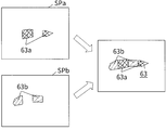
- the spherical concave defect 51 is illuminated by crossing the illumination lights from different directions of the lighting devices 2a and 2b arranged opposite to each other as shown in FIG.
- the positional relationship between the positions of the devices 2a and 2b and the reflection position is opposite. That is, in the aligned sub-pixel image 61, the bright points 61a and 61b corresponding to the lighting devices 2a and 2b do not overlap, and the bright points 61a and 61b are within a preset range, and are bright.
- the positions of the points 61a and 61b have a positional relationship opposite to the arrangement positions of the lighting devices 2a and 2b, it is determined to be a concave defect 51.
- the illumination light from the illumination devices 2a and 2b to the convex defect 52 does not cross, and the positional relationship between each position of the illumination devices 2a and 2b and the reflection position is Is the same. Therefore, in the aligned sub-pixel image 62, the bright points 62a and 62b corresponding to the lighting devices 2a and 2b do not overlap, and the bright points 62a and 62b are within the preset range, and are bright.
- the positions of the points 62a and 62b have the same positional relationship as the arrangement positions of the lighting devices 2a and 2b, it is determined to be a convex defect 52.
- FIGS. 10 and 11 bright points 61a and 62a corresponding to the lighting device 2a are shown by double hatching, and bright points 61b and 62b corresponding to the lighting device 2b are shown by broken line hatching. The same applies to FIGS. 12 and later.
- the illumination lights from the illumination devices 2a and 2b arranged to face each other cross each other, and the illumination devices 2a and 2b
- the positional relationship between each position and the reflection position is reversed.
- the directions of the scratched surfaces are not uniform, the reflection of the illumination light of the illumination device 2a and the reflection of the illumination light of the illumination device 2b coexist.
- the plane is a high reflectance surface, the illumination lights are mixed and not reflected.
- the bright points 63a corresponding to the lighting device 2a and the bright points 63b corresponding to the lighting device 2b do not overlap, and the bright points 63a and 63b are mixed, and the bright points 63a
- the position of 63b is opposite to the arrangement position of the lighting devices 2a and 2b, it is determined that the scratch defect 53 is present on the surface of the object 5 to be inspected.
- each illumination light is mixed and reflected by the defect 54. Will be done. Therefore, in the aligned sub-pixel image 64, when the bright points 64a and 64b corresponding to the lighting devices 2a and 2b overlap, it is determined that dust or dirt is present on the surface of the object 5 to be inspected.
- Each subpixel image by the lighting devices 2a and 2b is a dark field image, and unevenness defects, scratch defects, dust, dust, etc. appear as white spots. Defect candidates on the image are detected as follows.
- each subpixel image is binarized by B2, and the discrete pixel aggregation process is performed by the expansion / contraction process. Further, each pixel set is labeled by color coding or the like.
- W1 does not simply indicate the minimum defect size, but indicates the minimum size that can be regarded as a "defect portion".
- the size of the defect is defined as X or more in terms of the number of pixels
- each illumination is combined.
- the bright points 61a and 61b corresponding to the devices 2a and 2b do not overlap, the bright points 61a and 61b are within the range of the coordinates Vi ⁇ X / 2, and the positions of the bright points 61a and 61b are located in the lighting device 2a, Since the positional relationship is opposite to the arrangement position of 2b, it is determined to be a void defect.
- the respective lighting devices 2a and 2b are combined.
- the corresponding bright points 62a and 62b do not overlap, the bright points 62a and 62b are within the range of the coordinates Vi ⁇ X / 2, and the positions of the bright points 62a and 62b are the positions of the lighting devices 2a and 2b. Since they have the same positional relationship, it is determined to be a convex defect.
- the respective lighting devices 2a and 2b are combined.
- the corresponding bright points 62a and 62b are within the range of the coordinates Vi ⁇ X / 2, the bright points 62a and 62b are mixed without overlapping, and the positions of the bright points 63a and 63b are the arrangement positions of the lighting devices 2a and 2b. Since it is the opposite of the above, it is judged to be a scratch defect.
- the detection result is displayed on the display device 6.
- the display is preferably, together with the images after the alignment of the two subpixel images SPa and SPb shown on the right side of FIGS. 14 to 17, the type of the identified defect and the range of the coordinates Vi ⁇ X / 2 for each defect. May also be displayed.
- the present invention is not limited to the above embodiment.
- the line sensor 1 and the lighting devices 2a and 2b are fixed and the image is taken while moving the object 5 to be inspected.
- the object 5 to be inspected is fixed and the line sensor 1 and the lighting devices 2a and 2b are moved.
- the image may be taken while the image is being taken, as long as at least one of the object 5 to be inspected, the line sensor 1 and the lighting devices 2a and 2b is relatively moving with respect to the other.
- the relative moving distance of the non-inspected object 5 per shooting is A and the length of the subpixel 23 is 2A is shown. It suffices if the shooting ranges overlap and subpixels can be formed. Therefore, it is preferable that the relative movement distance of the non-inspected object 5 per photographing is 1/2 or less of one pixel.
- the present invention can be used to determine surface defects of an object to be inspected such as a product or part having a surface having a strong specular reflection property.
Landscapes
- Engineering & Computer Science (AREA)
- General Physics & Mathematics (AREA)
- Physics & Mathematics (AREA)
- General Health & Medical Sciences (AREA)
- Immunology (AREA)
- Chemical & Material Sciences (AREA)
- Analytical Chemistry (AREA)
- Biochemistry (AREA)
- Health & Medical Sciences (AREA)
- Pathology (AREA)
- Life Sciences & Earth Sciences (AREA)
- Textile Engineering (AREA)
- Computer Vision & Pattern Recognition (AREA)
- Signal Processing (AREA)
- Quality & Reliability (AREA)
- Theoretical Computer Science (AREA)
- Investigating Materials By The Use Of Optical Means Adapted For Particular Applications (AREA)
Abstract
Description
この発明は、正反射性状の強い表面を持つ製品や部品等の被検査物の表面欠陥を判別するための表面欠陥判別装置、この表面欠陥判別装置を備えた外観検査装置及びプログラムに関する。 The present invention relates to a surface defect discriminating device for discriminating surface defects of an object to be inspected such as a product or part having a surface having a strong specular reflection property, and an appearance inspection device and a program provided with this surface defect discriminating device.
製品や部品の表面にある傷は外観を損なう。また、フィルムのような薄膜を製膜するための成膜板に傷などに起因する凹凸がある場合は、製造した薄膜に凹凸が転写され薄膜の欠陥となってしまう。 Scratches on the surface of products and parts spoil the appearance. Further, when the film-forming plate for forming a thin film such as a film has irregularities due to scratches or the like, the irregularities are transferred to the manufactured thin film, resulting in defects in the thin film.
そこで、各種の製品や部品、成膜板等の表面欠陥を検出するための外観検査装置が提案されている。 Therefore, an appearance inspection device for detecting surface defects of various products, parts, film-forming plates, etc. has been proposed.
例えば特許文献1には、複数方向の光源を切り替えながら部品を撮影し、照明光源の方向とその撮影画像を解析することで、画像の影が欠陥なのか汚れなのかを判別することを特徴とする技術が開示されている。
For example,
しかしながら、特許文献1に記載の発明は、被検査物が静止していることを前提としており、例えば、静止制御が困難なドラム駆動されるベルト部品をベルトを動かしながら検査して、表面欠陥を判別することはできない。
However, the invention described in
このため、照明装置や画像を撮影するラインセンサに対して、被検査物を相対的に移動させながら、表面欠陥を判別できる技術が望まれている。 Therefore, there is a demand for a technique capable of discriminating surface defects while moving the object to be inspected relative to a lighting device or a line sensor that captures an image.
この発明は、このような技術的背景に鑑みてなされたものであって、照明装置及びラインセンサに対して、被検査物を相対的に移動させながら、表面欠陥を判別できる表面欠陥判別装置、外観検査装置及びプログラムの提供を目的とする。 The present invention has been made in view of such a technical background, and is a surface defect discriminating device capable of discriminating surface defects while relatively moving an object to be inspected with respect to a lighting device and a line sensor. The purpose is to provide visual inspection equipment and programs.
上記目的は以下の手段によって達成される。
(1)異なる位置に配置された照明装置及びラインセンサに対して被検査物を相対的に移動させながら、前記各照明装置からの照明光を1つずつ切り替えて被検査物に照射させたときに、各照明装置からの照明光が切り替えられる毎に、被検査物からの反射光をラインセンサで受光して撮影することにより、前記照明光の切り替え分だけそれぞれ位置ずれした状態で複数の画像を取得する画像取得手段と、前記画像取得手段により取得された、各照明装置に対応する画像を位置合わせする位置合わせ手段と、前記位置合わせ手段により位置合わせされた画像から、被検査物の表面欠陥を判別する判別手段と、を備えた表面欠陥判別装置。
(2)前記ラインセンサの各画素の一部は、1つの前記照明装置による照明光が被検査物に照射されることによる今回の撮影と前回の撮影とで撮影範囲が重複する重複領域となっており、1つの画素における前記重複領域を除く部分をサブピクセルとするとき、今回の撮影での画素全体の受光量から前記重複領域の受光量を差し引くことで、今回のサブピクセルの受光量を推定しサブピクセル画像を作成するサブピクセル画像作成手段と、を備え、前記位置合わせ手段は、前記サブピクセル画像作成手段により作成された各照明装置に対応するサブピクセル画像を位置合わせする請求項1に記載の表面欠陥判別装置。
(3)異なる位置に配置された照明装置及びラインセンサに対して被検査物を相対的に移動させながら、前記各照明装置からの照明光を1つずつ切り替えて被検査物に照射させたときに、各照明装置からの照明光が切り替えられる毎に、被検査物からの反射光をラインセンサで受光して撮影することにより、前記各照明光毎に複数の画像を取得する画像取得手段を備え、前記ラインセンサの各画素の一部は、1つの前記照明装置による照明光が被検査物に照射されることによる今回の撮影と前回の撮影とで撮影範囲が重複する重複領域となっており、1つの画素における前記重複領域を除く部分をサブピクセルとするとき、今回の撮影での画素全体の受光量から前記重複領域の受光量を差し引くことで、今回のサブピクセルの受光量を推定しサブピクセル画像を作成するサブピクセル画像作成手段と、サブピクセル画像作成手段により作成されたサブピクセル画像に基づいて、被検査物の表面欠陥を判別する判別手段と、をさらに備えている表面欠陥判別装置。
(4)前記サブピクセル画像作成手段により作成された各照明装置に対応するサブピクセル画像を位置合わせする位置合わせ手段を備えている前項3に記載の表面欠陥判別装置。
(5)前記サブピクセル画像作成手段は、前記重複領域の受光量を領域毎に補正した状態で、画素全体の受光量から差し引く前項2~4のいずれかに記載の表面欠陥判別装置。
(6)前記サブピクセル画像作成手段は、前記重複領域の受光量を、前回以前に推定されたサブピクセルの受光量の和から求め、求めた受光量を画素全体の受光量から差し引いて今回のサブピクセルの受光量を推定する前項2~5のいずれかに記載の表面欠陥判別装置。
(7)前記サブピクセル画像作成手段は、撮影開始後の最初の画素全体の受光量を1画素あたりのサブピクセルの数で割った平均値を、最初のサブピクセルの受光量と推定する前項6に記載の表面欠陥判別装置。
(8)前記サブピクセル画像作成手段は、画素全体の受光量が所定の閾値を超えない場合、画素全体の受光量を1画素あたりのサブピクセルの数で割った平均値を、今回のサブピクセルの受光量と推定し、画素全体の受光量が所定の閾値を超える場合、画素全体の受光量から前記重複領域の受光量を差し引くことで、今回のサブピクセルの受光量を推定する前項2~7のいずれかに記載の表面欠陥判別装置。
(9)前記位置合わせ手段は、前記サブピクセル画像作成手段により作成された各照明装置に対応するサブピクセル画像の位置合わせを、下記式により輝度値Ki
jを補正値K'i
jに補正することにより行う前項2、4~8のいずれかに記載の表面欠陥判別装置。
The above object is achieved by the following means.
(1) When the object to be inspected is irradiated by switching the illumination light from each of the lighting devices one by one while moving the object to be inspected relative to the illumination devices and line sensors arranged at different positions. In addition, each time the illumination light from each illumination device is switched, the reflected light from the object to be inspected is received by the line sensor and photographed, so that a plurality of images are displaced by the switching amount of the illumination light. The surface of the object to be inspected from the image acquisition means for acquiring the image, the alignment means for aligning the image corresponding to each lighting device acquired by the image acquisition means, and the image aligned by the alignment means. A surface defect discriminating device including a discriminating means for discriminating defects.
(2) A part of each pixel of the line sensor is an overlapping region in which the shooting range overlaps between the current shooting and the previous shooting due to the illumination light from one of the lighting devices irradiating the object to be inspected. When the portion of one pixel excluding the overlapping region is a sub-pixel, the light receiving amount of the sub-pixel this time is obtained by subtracting the light receiving amount of the overlapping region from the light receiving amount of the entire pixel in the current shooting. A sub-pixel image creating means for estimating and creating a sub-pixel image, and the aligning means aligns a sub-pixel image corresponding to each lighting device created by the sub-pixel image creating means. The surface defect discriminating device according to.
(3) When the object to be inspected is irradiated by switching the illumination light from each of the illumination devices one by one while moving the object to be inspected relative to the illumination devices and line sensors arranged at different positions. In addition, each time the illumination light from each illumination device is switched, the image acquisition means for acquiring a plurality of images for each illumination light by receiving the reflected light from the object to be inspected by the line sensor and taking a picture is provided. In addition, a part of each pixel of the line sensor becomes an overlapping area where the shooting range overlaps between the current shooting and the previous shooting due to the illumination light from one of the lighting devices irradiating the object to be inspected. When the portion of one pixel excluding the overlapping region is a sub-pixel, the light receiving amount of the sub-pixel this time is estimated by subtracting the received light amount of the overlapping region from the received light amount of the entire pixel in the current shooting. A surface defect further comprising a sub-pixel image creating means for creating a sub-pixel image and a discriminating means for determining a surface defect of an object to be inspected based on the sub-pixel image created by the sub-pixel image creating means. Discriminating device.
(4) The surface defect determining device according to
(5) The surface defect determining device according to any one of
(6) The sub-pixel image creating means obtains the light-receiving amount in the overlapping region from the sum of the light-receiving amounts of the sub-pixels estimated before the previous time, and subtracts the obtained light-receiving amount from the light-receiving amount of the entire pixel. The surface defect discriminating device according to any one of
(7) The subpixel image creating means estimates that the average value obtained by dividing the light receiving amount of the entire first pixel after the start of shooting by the number of subpixels per pixel is the light receiving amount of the first subpixel. The surface defect discriminating device according to.
(8) In the sub-pixel image creating means, when the light-receiving amount of the entire pixel does not exceed a predetermined threshold value, the average value obtained by dividing the light-receiving amount of the entire pixel by the number of sub-pixels per pixel is divided by the number of sub-pixels per pixel. When the light receiving amount of the entire pixel exceeds a predetermined threshold value, the light receiving amount of the sub-pixel this time is estimated by subtracting the light receiving amount of the overlapping region from the light receiving amount of the entire pixel. 7. The surface defect discriminating device according to any one of 7.
(9) the alignment means, the alignment of the sub-pixel image corresponding to each illumination device created by the sub-pixel image creating means, the correction in the correction value K 'i j luminance value K i j by the following formula The surface defect discriminating device according to any one of 2, 4 to 8 in the preceding item.

ただし、i:サブピクセル推定位置のインデックス
j:点灯している照明装置の識別番号
(10)前記判別手段は、前記位置合わせ手段により位置合わせされたサブピクセル画像において、各照明装置に対応する明点が重複せずかつ各明点が予め設定された範囲内にある場合は、被検査物の表面に凹欠陥または凸欠陥が存在すると判定する前項1、2、4~9のいずれかに記載の表面欠陥判別装置。
(11)前記判別手段は、前記位置合わせ手段により位置合わせされたサブピクセル画像において、各照明装置に対応する明点の位置が照明装置の配置位置と逆である場合は凹欠陥が存在し、逆でない場合は凸欠陥が存在すると判定する前項10に記載の表面欠陥判別装置。
(12)前記判別手段は、前記位置合わせ手段により位置合わせされたサブピクセル画像において、各照明装置に対応する明点が重複しているときは、被検査物の表面にゴミまたはほこりが存在すると判定する前項1、2、4~11のいずれかに記載の表面欠陥判別装置。
(13)全体の受光量が所定の閾値を超える画素を欠陥候補画素として検出し、検出された欠陥候補画素について、前記位置合わせ手段によりサブピクセル画像を位置合わせし、かつ判定手段により被検査物の表面欠陥を判別する前項12、4~12のいずれかに記載の表面欠陥判別装置。
(14)前記照明装置の光源として、LEDまたは可視光半導体レーザーが用いられる前項1~13のいずれかに記載の表面欠陥判別装置。
(15)前記照明装置は3個以上であり、前記ラインセンサを中心とする円周上でかつ、360度÷照明装置の数、の角度差で配置されている前項1~14のいずれかに記載の表面欠陥判別装置。
(16)異なる位置に配置された複数の照明装置と、各照明装置から被検査物に照射された照明光の反射光を受光可能なラインセンサと、前記被検査物を、前記照明装置及びラインセンサに対して相対的に移動させる移動手段と、各照明装置からの照明光を1つずつ所定の周期で切り替えて被検査物に照射させる照明制御手段と、前記移動手段により、前記被検査物を前記照明装置及びラインセンサに対して相対的に移動させながら、前記照明制御手段により、各照明装置からの照明光が切り替えられる毎に、被検査物からの反射光を受光して撮影を行うように、前記ラインセンサを制御するラインセンサ制御手段と、前項1~15のいずれかに記載の表面欠陥判別装置と、を備えた外観検査装置。
(17)異なる位置に配置された照明装置及びラインセンサに対して被検査物を相対的に移動させながら、前記各照明装置からの照明光を1つずつ切り替えて被検査物に照射させたときに、各照明装置からの照明光が切り替えられる毎に、被検査物からの反射光をラインセンサで受光して撮影することにより、前記照明光の切り替え分だけそれぞれ位置ずれした状態で複数の画像を取得する画像取得ステップと、前記画像取得ステップにより取得された、各照明装置に対応する画像を位置合わせする位置合わせステップと、前記位置合わせステップにより位置合わせされた画像から、被検査物の表面欠陥を判別する判別ステップと、をコンピュータに実行させるためのプログラム。
(18)前記ラインセンサの各画素の一部は、1つの前記照明装置による照明光が被検査物に照射されることによる今回の撮影と前回の撮影とで撮影範囲が重複する重複領域となっており、1つの画素における前記重複領域を除く部分をサブピクセルとするとき、今回の撮影での画素全体の受光量から前記重複領域の受光量を差し引くことで、今回のサブピクセルの受光量を推定しサブピクセル画像を作成するサブピクセル画像作成ステップを前記コンピュータに実行させ、前記位置合わせステップでは、前記サブピクセル画像作成ステップにより作成された各照明装置に対応するサブピクセル画像を位置合わせする処理を前記コンピュータに実行させる前項17に記載のプログラム。
(19)前記サブピクセル画像作成ステップでは、前記重複領域の受光量を領域毎に補正した状態で、画素全体の受光量から差し引く処理を前記コンピュータに実行させる前項17に記載のプログラム。
(20)前記サブピクセル画像作成ステップでは、前記重複領域の受光量を、前回以前に推定されたサブピクセルの受光量の和から求め、求めた受光量を画素全体の受光量から差し引いて今回のサブピクセルの受光量を推定する処理を前記コンピュータに実行させる前項18または19に記載のプログラム。
(21)前記サブピクセル画像作成ステップでは、撮影開始後の最初の画素全体の受光量を1画素あたりのサブピクセルの数で割った平均値を、最初のサブピクセルの受光量と推定する処理を前記コンピュータに実行させる前項20に記載のプログラム。
(22)前記サブピクセル画像作成ステップでは、画素全体の受光量が所定の閾値を超えない場合、画素全体の受光量を1画素あたりのサブピクセルの数で割った平均値を、今回のサブピクセルの受光量と推定し、画素全体の受光量が所定の閾値を超える場合、画素全体の受光量から前記重複領域の受光量を差し引くことで、今回のサブピクセルの受光量を推定する処理を前記コンピュータに実行させる前項18~21のいずれかに記載のプログラム。
(23)前記位置合わせステップでは、前記サブピクセル画像作成ステップにより作成された各照明装置に対応するサブピクセル画像の位置合わせを、下記式により輝度値Ki
jを補正値K'i
jに補正することにより行う処理を前記コンピュータに実行させる前項18~22のいずれかに記載のプログラム。
However, i: index of the estimated sub-pixel position j: identification number of the lit lighting device (10) The discriminating means corresponds to each lighting device in the sub-pixel image aligned by the positioning means. If the points do not overlap and each bright point is within a preset range, it is described in any one of the
(11) The discriminating means has a concave defect when the position of the bright point corresponding to each illuminating device is opposite to the arranging position of the illuminating device in the subpixel image aligned by the positioning means. The surface defect discriminating device according to
(12) The discriminating means determines that dust or dirt is present on the surface of the object to be inspected when the bright spots corresponding to the lighting devices overlap in the subpixel image aligned by the positioning means. Judgment The surface defect discriminating device according to any one of the preceding
(13) A pixel whose total received light amount exceeds a predetermined threshold value is detected as a defect candidate pixel, a subpixel image is aligned with the detected defect candidate pixel by the alignment means, and an object to be inspected by a determination means. The surface defect discriminating device according to any one of the
(14) The surface defect determination device according to any one of
(15) The number of the lighting devices is three or more, and any of the
(16) A plurality of lighting devices arranged at different positions, a line sensor capable of receiving the reflected light of the illumination light emitted from each lighting device to the object to be inspected, and the lighting device and the line of the object to be inspected. The moving means for moving relative to the sensor, the lighting control means for switching the illumination light from each lighting device one by one at a predetermined cycle to irradiate the object to be inspected, and the moving means for the object to be inspected. Is moved relative to the lighting device and the line sensor, and each time the lighting light from each lighting device is switched by the lighting control means, the reflected light from the object to be inspected is received and photographed. As described above, an appearance inspection device including the line sensor control means for controlling the line sensor and the surface defect determination device according to any one of the
(17) When the object to be inspected is irradiated by switching the illumination light from each of the illumination devices one by one while moving the object to be inspected relative to the illumination devices and line sensors arranged at different positions. In addition, each time the illumination light from each illumination device is switched, the reflected light from the object to be inspected is received by the line sensor and photographed, so that a plurality of images are displaced by the switching amount of the illumination light. From the image acquisition step for acquiring the image, the alignment step for aligning the image corresponding to each lighting device acquired by the image acquisition step, and the image aligned by the alignment step, the surface of the object to be inspected. A program that causes a computer to perform a determination step that determines defects.
(18) A part of each pixel of the line sensor is an overlapping region in which the shooting range overlaps between the current shooting and the previous shooting due to the illumination light from one of the lighting devices irradiating the object to be inspected. When the portion of one pixel excluding the overlapping region is a sub-pixel, the light receiving amount of the sub-pixel this time is obtained by subtracting the light receiving amount of the overlapping region from the light receiving amount of the entire pixel in the current shooting. A process of causing the computer to execute a sub-pixel image creation step of estimating and creating a sub-pixel image, and in the alignment step, aligning a sub-pixel image corresponding to each lighting device created by the sub-pixel image creation step. The program according to the preceding item 17, which causes the computer to execute the above.
(19) The program according to the preceding item 17, wherein in the sub-pixel image creation step, the computer is made to execute a process of subtracting from the light-receiving amount of the entire pixel in a state where the light-receiving amount of the overlapping region is corrected for each area.
(20) In the sub-pixel image creation step, the light-receiving amount in the overlapping region is obtained from the sum of the light-receiving amounts of the sub-pixels estimated before the previous time, and the obtained light-receiving amount is subtracted from the light-receiving amount of the entire pixel to obtain this time. The program according to item 18 or 19 above, which causes the computer to execute a process of estimating the amount of light received by a subpixel.
(21) In the subpixel image creation step, a process of estimating the light receiving amount of the first subpixel is the average value obtained by dividing the light receiving amount of the entire first pixel after the start of shooting by the number of subpixels per pixel. The program according to
(22) In the sub-pixel image creation step, when the light-receiving amount of the entire pixel does not exceed a predetermined threshold value, the average value obtained by dividing the light-receiving amount of the entire pixel by the number of sub-pixels per pixel is the current sub-pixel. When the light receiving amount of the entire pixel exceeds a predetermined threshold value, the light receiving amount of the sub-pixel this time is estimated by subtracting the light receiving amount of the overlapping region from the light receiving amount of the entire pixel. The program according to any one of items 18 to 21 above, which is to be executed by a computer.
(23) In the positioning step, the alignment of the sub-pixel image corresponding to each illumination device created by the sub-pixel image generating step, correcting the luminance value K i j of the correction value K 'i j by the following formula The program according to any one of items 18 to 22 above, which causes the computer to execute the processing performed by the operation.

ただし、i:サブピクセル推定位置のインデックス
j:点灯している照明の識別差番号
(24)前記判別ステップでは、前記位置合わせステップにより位置合わせされたサブピクセル画像において、各照明装置に対応する明点が重複せずかつ各明点が予め設定された範囲内にある場合は、被検査物の表面に凹欠陥または凸欠陥が存在すると判定する処理を前記コンピュータに実行させる前項17~23のいずれかに記載のプログラム。
(25)前記判別ステップでは、前記位置合わせステップにより位置合わせされたサブピクセル画像において、前記位置合わせ手段により位置合わせされたサブピクセル画像において、各照明装置に対応する明点の位置が照明装置の配置位置と逆である場合は凹欠陥が存在し、逆でない場合は凸欠陥が存在すると判定する処理を前記コンピュータに実行させる前項24に記載のプログラム。
(26)前記判別ステップでは、前記位置合わせステップにより位置合わせされたピクセル画像において、各照明装置に対応する明点が重複しているときは、被検査物の表面にゴミまたはほこりが存在すると判定する処理を前記コンピュータに実行させる前項17~25のいずれかに記載のプログラム。
(27)全体の受光量が所定の閾値を超える画素を欠陥候補画素として検出し、検出された欠陥候補画素について、前記位置合わせ手段によりサブピクセル画像を位置合わせし、かつ判定ステップにより被検査物の表面欠陥を判別する処理を前記コンピュータに実行させる前項17~26のいずれかに記載のプログラム。
(28)前記照明装置の光源として、LEDまたは可視光半導体レーザーが用いられる前項17~27のいずれかに記載のプログラム。
(29)複数個の前記照明装置は、前記ラインセンサを中心とする円周上かつ360度/(照明装置の個数)の位置に配置されている前項17~28のいずれかに記載のプログラム。
However, i: index of the estimated subpixel position j: identification difference number of the lit lighting (24) In the discrimination step, in the subpixel image aligned by the alignment step, the brightness corresponding to each lighting device is provided. If the points do not overlap and each bright point is within a preset range, any of 17 to 23 in the preceding paragraph, which causes the computer to execute a process of determining that a concave defect or a convex defect exists on the surface of the object to be inspected. The program described in Crab.
(25) In the determination step, in the subpixel image aligned by the alignment step, in the subpixel image aligned by the alignment means, the position of the bright point corresponding to each illumination device is the position of the illumination device. The program according to item 24 above, which causes the computer to execute a process of determining that a concave defect exists when the position is opposite to the arrangement position and a convex defect exists when the position is not the opposite.
(26) In the determination step, when the bright spots corresponding to the lighting devices overlap in the pixel image aligned by the alignment step, it is determined that dust or dirt is present on the surface of the object to be inspected. The program according to any one of 17 to 25 in the preceding paragraph, which causes the computer to execute the process to be performed.
(27) A pixel whose total received light amount exceeds a predetermined threshold value is detected as a defect candidate pixel, a subpixel image is aligned with the detected defect candidate pixel by the alignment means, and an object to be inspected is subjected to a determination step. The program according to any one of 17 to 26 in the preceding paragraph, which causes the computer to execute a process for determining a surface defect of the above.
(28) The program according to any one of 17 to 27 above, wherein an LED or a visible light semiconductor laser is used as a light source of the lighting device.
(29) The program according to any one of items 17 to 28 above, wherein the plurality of lighting devices are arranged on a circumference centered on the line sensor and at a position of 360 degrees / (number of lighting devices).
前項(1)に記載の発明によれば、異なる位置に配置された照明装置及びラインセンサに対して被検査物を相対的に移動させながら、各照明装置からの照明光が1つずつ切り替えて被検査物に照射される。各照明装置からの照明光が切り替えられる毎に、被検査物からの反射光をラインセンサで受光して撮影することにより、照明光の切り替え分だけそれぞれ位置ずれした状態で複数の画像が取得される。取得された各照明装置に対応する画像は位置合わせされたのち、位置合わせされた画像から被検査物の表面欠陥が判別される。 According to the invention described in the preceding paragraph (1), the illumination light from each illumination device is switched one by one while the object to be inspected is relatively moved with respect to the illumination devices and line sensors arranged at different positions. The object to be inspected is irradiated. Each time the illumination light from each illumination device is switched, the reflected light from the object to be inspected is received by the line sensor and photographed, so that a plurality of images are acquired in a state of being displaced by the amount of switching of the illumination light. To. The acquired image corresponding to each lighting device is aligned, and then the surface defect of the object to be inspected is determined from the aligned image.
このように、照明装置及びラインセンサに対して被検査物が相対的に移動しているために、各照明装置からの照明光が切り替えられたときの照明光の切り替え分だけそれぞれ位置ずれした状態で、ラインセンサから取得された各照明装置に対応する複数の画像が位置合わせされ、この位置合わせされた状態で被検査物の表面欠陥が判別されるから、被検査物を相対的に移動させながら、被検査物の表面欠陥を判別することができる。 In this way, since the object to be inspected is moving relative to the lighting device and the line sensor, the positions of the objects to be inspected are displaced by the amount of switching of the lighting light when the lighting light from each lighting device is switched. Then, a plurality of images corresponding to each lighting device acquired from the line sensor are aligned, and the surface defect of the inspected object is determined in this aligned state. Therefore, the inspected object is relatively moved. However, the surface defect of the object to be inspected can be discriminated.
前項(2)に記載の発明によれば、ラインセンサの各画素の一部は、1つの照明装置による照明光が被検査物に照射されることによる今回の撮影と前回の撮影とで撮影範囲が重複する重複領域となっており、1つの画素における重複領域を除く部分をサブピクセルとするとき、今回の撮影での画素全体の受光量から重複領域の受光量を差し引くことで、今回のサブピクセルの受光量が推定され、サブピクセル画像が作成される。そして、作成された各照明装置に対応するサブピクセル画像を位置合わせし、位置合わせされた画像から被検査物の表面欠陥が検出される。ここで、サブピクセルは、画素における重複領域を除く部分であるから、1画素より小さく、このため外観検査の分解能が向上し、より細かい表面欠陥の検出を行うことができる。 According to the invention described in the previous section (2), a part of each pixel of the line sensor has a shooting range in the current shooting and the previous shooting when the object to be inspected is irradiated with the illumination light by one lighting device. Is an overlapping area, and when the part of one pixel excluding the overlapping area is a sub-pixel, the sub-pixel of this time is obtained by subtracting the light-receiving amount of the overlapping area from the light-receiving amount of the entire pixel in this shooting. The amount of light received by the pixel is estimated and a subpixel image is created. Then, the sub-pixel image corresponding to each created lighting device is aligned, and the surface defect of the object to be inspected is detected from the aligned image. Here, since the sub-pixel is a portion of the pixel excluding the overlapping region, it is smaller than one pixel, so that the resolution of the visual inspection is improved and finer surface defects can be detected.
つまり、相対的に移動する非検査物をラインセンサで撮影する場合、ラインセンサと非検査物の撮影面間の距離が安定せず、被写界深度を深く設定する必要があるが、被写界深度を深くすると分解能が下がるトレードオフの関係があり、細かい欠陥まで検査できない場合があるが、1画素より小さいサブピクセルの画像を使用することにより、被写界深度を深くしなくても分解能が上がり、より細かい欠陥まで検査できる利点がある。 In other words, when shooting a relatively moving non-inspected object with a line sensor, the distance between the line sensor and the imaging surface of the non-inspected object is not stable, and it is necessary to set the depth of field deeply. There is a trade-off relationship that the resolution decreases when the depth of field is increased, and it may not be possible to inspect even small defects. However, by using an image with sub-pixels smaller than one pixel, the resolution can be achieved without increasing the depth of field. There is an advantage that even finer defects can be inspected.
前項(3)に記載の発明によれば、1画素より小さいサブピクセル画像から欠陥が判別されるから、外観検査の分解能が向上し、より細かい表面欠陥の検出を行うことができる。 According to the invention described in the preceding paragraph (3), since defects are discriminated from subpixel images smaller than one pixel, the resolution of visual inspection is improved and finer surface defects can be detected.
前項(4)に記載の発明によれば、各照明装置に対応するサブピクセル画像の位置合わせにより、さらに精度の良い欠陥検出が可能となる。 According to the invention described in the preceding paragraph (4), more accurate defect detection is possible by aligning the subpixel image corresponding to each lighting device.
前項(5)に記載の発明によれば、重複領域の受光量を領域毎に補正した状態で、画素全体の受光量から差し引かれるから、重複領域のより正確な受光量を差し引いて今回のサブピクセルの受光量を推定でき、ひいてはより精度の高い欠陥判別を行うことができる。 According to the invention described in the previous section (5), the light receiving amount of the overlapping region is corrected for each region and is subtracted from the light receiving amount of the entire pixel. Therefore, the more accurate light receiving amount of the overlapping region is subtracted to make this sub. The amount of light received by the pixels can be estimated, and as a result, more accurate defect discrimination can be performed.
前項(6)に記載の発明によれば、重複領域の受光量を、前回以前に推定されたサブピクセルの受光量の和から求め、求めた受光量を画素全体の受光量から差し引いて今回のサブピクセルの受光量を推定するから、推定処理が簡素化される。 According to the invention described in the previous section (6), the amount of light received in the overlapping region is obtained from the sum of the amount of light received by the subpixels estimated before the previous time, and the obtained amount of light received is subtracted from the amount of light received by the entire pixel. Since the amount of light received by the subpixel is estimated, the estimation process is simplified.
前項(7)に記載の発明によれば、撮影開始後の最初の画素全体の受光量を1画素あたりのサブピクセルの数で割った平均値を、最初のサブピクセルの受光量と推定するから、次回以降のサブピクセルの受光量の推定処理をスムーズに行うことができる。 According to the invention described in the previous section (7), the average value obtained by dividing the light receiving amount of the entire first pixel after the start of shooting by the number of subpixels per pixel is estimated as the light receiving amount of the first subpixel. , It is possible to smoothly estimate the light receiving amount of the subpixel from the next time onward.
前項(8)に記載の発明によれば、画素全体の受光量が所定の閾値を超えない場合、換言すれば表面欠陥が存在しない可能性が高い場合は、画素全体の受光量を1画素あたりのサブピクセルの数で割った平均値を、今回のサブピクセルの受光量と推定する。一方、画素全体の受光量が所定の閾値を超える場合、換言すれば表面欠陥が存在する可能性が高い場合は、画素全体の受光量から前記重複領域の受光量を差し引くことで、今回のサブピクセルの受光量が推定される。これによって、表面欠陥が存在する可能性が高い領域に集中して欠陥判別処理を実行することができる。 According to the invention described in the previous section (8), when the light receiving amount of the entire pixel does not exceed a predetermined threshold value, in other words, when there is a high possibility that surface defects do not exist, the light receiving amount of the entire pixel is per pixel. The average value divided by the number of sub-pixels in is estimated as the amount of light received by the sub-pixels this time. On the other hand, when the light receiving amount of the entire pixel exceeds a predetermined threshold value, in other words, when there is a high possibility that a surface defect exists, the light receiving amount of the overlapping region is subtracted from the light receiving amount of the entire pixel, so that the sub The amount of light received by the pixel is estimated. As a result, the defect discrimination process can be executed by concentrating on the region where the surface defects are likely to exist.
前項(9)に記載の発明によれば、各照明装置に対応するサブピクセル画像の位置合わせを正確に行うことができ、ひいては精度の高い欠陥判別を行うことができる。 According to the invention described in the preceding paragraph (9), the subpixel image corresponding to each lighting device can be accurately aligned, and the defect can be discriminated with high accuracy.
前項(10)に記載の発明によれば、被検査物の表面の傷等の凹欠陥または凸欠陥を判別することができる。 According to the invention described in the preceding paragraph (10), it is possible to discriminate concave defects or convex defects such as scratches on the surface of the object to be inspected.
前項(11)に記載の発明によれば、被検査物の表面の凹欠陥や凸欠陥を判別することができる。 According to the invention described in the preceding paragraph (11), it is possible to discriminate concave defects and convex defects on the surface of the object to be inspected.
前項(12)に記載の発明によれば、被検査物の表面のゴミまたはほこりを判別することができる。 According to the invention described in the preceding paragraph (12), it is possible to discriminate dust or dirt on the surface of the object to be inspected.
前項(13)に記載の発明によれば、全体の受光量が所定の閾値を超える画素を欠陥候補画素として検出し、検出された欠陥候補画素について、サブピクセル画像を位置合わせし、かつ被検査物の表面欠陥を判別するから、表面欠陥が存在する可能性が高い領域に集中して欠陥判別処理を実行することができる。 According to the invention described in the previous section (13), a pixel whose total received light amount exceeds a predetermined threshold value is detected as a defect candidate pixel, and a subpixel image is aligned with the detected defect candidate pixel and is inspected. Since the surface defects of the object are discriminated, the defect discriminating process can be executed by concentrating on the region where the surface defects are likely to exist.
前項(14)に記載の発明によれば、LEDまたは可視光半導体レーザーが照明装置の光源として用いられるから、各照明装置の切り替えを高速度で行うことができる。 According to the invention described in the preceding paragraph (14), since the LED or the visible light semiconductor laser is used as the light source of the lighting device, each lighting device can be switched at a high speed.
前項(15)に記載の発明によれば、照明装置は3個以上であり、ラインセンサを中心とする円周上でかつ、360度÷照明装置の数、の角度差で配置されているから、証明光が傷等と直角にならない照明装置が必ず確保され、傷等の表面欠陥を精度良く判別することができる。 According to the invention described in the preceding paragraph (15), the number of lighting devices is three or more, and they are arranged on the circumference centered on the line sensor with an angle difference of 360 degrees ÷ the number of lighting devices. A lighting device whose certification light is not perpendicular to scratches or the like is always secured, and surface defects such as scratches can be accurately discriminated.
前項(16)に記載の発明によれば、異なる位置に配置された照明装置及びラインセンサに対して被検査物を相対的に移動させながら、非検査物の表面欠陥判別を精度良く行うことができる外観検査装置となる。 According to the invention described in the preceding paragraph (16), it is possible to accurately determine the surface defect of the non-inspected object while moving the object to be inspected relative to the lighting device and the line sensor arranged at different positions. It becomes a visual inspection device that can be used.
前項(17)~(29)に記載の発明によれば、異なる位置に配置された照明装置及びラインセンサに対して被検査物を相対的に移動させながら、非検査物の表面欠陥判別処理をコンピュータに実行させることができる。 According to the inventions described in the preceding paragraphs (17) to (29), the surface defect determination process of the non-inspected object is performed while the inspected object is relatively moved with respect to the lighting device and the line sensor arranged at different positions. You can let the computer do it.
以下、この発明の実施形態を図面に基づいて説明する。
[外観検査装置の構成]
図1は、この発明の一実施形態に係る外観検査装置の構成図である。図1に示すように、外観検査装置は、ラインセンサ1と、2つの照明装置2a、2bと、各照明装置2a、2bを制御する照明制御部8と、ラインセンサ1を制御するラインセンサ制御部9と、被検査物5を搬送する搬送ドラム3、3と、被検査物5の撮影位置を検出するドラムエンコーダー4と、表示装置6と、コンピュータ10と、被検査物5の搬送速度の制御のために搬送ドラム3の回転数を制御する搬送ドラム制御部11等を備えている。
Hereinafter, embodiments of the present invention will be described with reference to the drawings.
[Configuration of visual inspection equipment]
FIG. 1 is a configuration diagram of an appearance inspection device according to an embodiment of the present invention. As shown in FIG. 1, the visual inspection device includes a
コンピュータ10は、ラインセンサ1で撮影された画像を処理して欠陥判別を行うとともに、照明装置2a、2bとラインセンサ1を同期制御する。また、表示装置6は、コンピュータ10により欠陥判別処理された画像と処理結果等を表示する。
The
被検査物5は高反射率のベルト状をなし、搬送ドラム3を使用してロール状に設置され、搬送ドラム3、3の矢印方向の回転によって、Y方向に送られるようになっている。ラインセンサ1による被検査物5の撮影位置は、ドラムエンコーダー4で検知される。
The
ラインセンサ1は、被検査物5の移動方向Yと直交するX方向に延設されており、2つの照明装置2a、2bは、図2(A)に示すように、上方から見てラインセンサ1を中心とする対象位置に180度の角度差で配置されており、それぞれ異なる2方向から照明することが可能である。照明装置2a、2bの対向方向はX方向でもY方向でも、他の方向でもかまわない。この実施形態では、2つの照明装置2a、2bを使用しているが、3つ以上を使用しても良い。3つ以上の場合、図2(B)に示すように、上方から見てラインセンサ1を中心とする円周上で、かつ360度÷照明装置の数、の角度差で配置されるのが、直線状の傷等の表面欠陥に対して直角にならない照明装置が必ず確保され、傷等の表面欠陥を精度良く判別することができる点から望ましい。なお、図2(B)では3つの照明装置2a、2b、2cの場合であり、相互に120度の角度差で配置されている。
The
各照明装置2a、2bは、照明制御部8での制御により任意のタイミングにてオンオフを切り替えることができるようになっている。
Each of the
ラインセンサ1の1ラインでの撮影範囲が、被検査物5に対して小さい場合は、Y方向に被検査物5を一回り撮影後、センサ照明搬送部12により、照明装置2a、2bとラインセンサ1を一体で、ラインセンサ1の長さ分X方向に移動させ、再度Y方向に一回り撮影し、これを順次繰り返すことで、被検査物5の全体を撮影する構成としても良い。
When the photographing range of one line of the
ラインセンサ1は、被検査物5をY方向に移動させながら、各照明装置2a、2bのオンオフを切り替えて被検査物5を照明したときの反射光を受光する。ラインセンサ1と各照明装置2a、2bは正対位置になく、各照明装置2a、2bからの照明光が被検査物5で乱反射された反射光がラインセンサ1に受光される。従って、ラインセンサ1により撮影される画像は暗視野画像となる。
The
被検査物5の表面は高反射率であるため、照明位置に凹欠陥、凸欠陥、傷状欠陥、ほこり、ゴミ等があった場合、これら欠陥、ほこり、ゴミ等で乱反射した反射光がラインセンサ1に入射する。
Since the surface of the object to be inspected 5 has high reflectance, if there are concave defects, convex defects, scratch defects, dust, dust, etc. at the illumination position, the reflected light diffusely reflected by these defects, dust, dust, etc. is lined up. It is incident on the
ラインセンサ制御部9と照明制御部8はコンピュータ10に接続され、ラインセンサ1と照明装置2a、ラインセンサ1と照明装置2bはそれぞれ同期して発光、撮影される。
The line
この実施形態では、一般的なラインセンサの仕様からラインセンサ1のラインレートを100kHz(シャッタースピード0.01ms)とする。つまり、照明装置2a、照明装置2bとして、0.01msごとに交互に高速に切り替えられるLED光源やLD(可視光半導体レーザー)光源などを用いたものが好適である。
[表面欠陥判別処理]
次に、コンピュータ10による被検査物5の表面欠陥判別処理について説明する。なお、コンピュータ10には、CPU、RAM、記憶装置等が備えられ、表面欠陥判別処理は、記憶装置等に格納された動作プログラムに従ってCPUが動作することにより実行される。
In this embodiment, the line rate of the
[Surface defect discrimination process]
Next, the surface defect discrimination process of the
前述したように、ラインセンサ1による撮影は、被検査物5を移動させながら、複数(この実施形態では2つ)の照明装置2a、2bのオンオフを交互に切り替えることにより行われる。コンピュータ10は、ラインセンサ1による撮影画像を順次取得する。
<サブピクセル画像の作成>
図3は、照明装置2a、2bを切り替えながら撮影するときの撮影範囲と画素20の相対的位置関係を説明するための図である。
As described above, the photographing by the
<Creation of subpixel image>
FIG. 3 is a diagram for explaining the relative positional relationship between the shooting range and the
図3に示すように、検出する欠陥30のサイズを12A、ラインセンサ1の分解能(1画素20の長さ)を6Aとし、被検査物5をA送るごとに照明装置2a、2bを切り替えながら撮影するものとする。ラインセンサ1の分解能6Aは、1画素における1回の撮影領域である。従って、図3に示すように、1回目の撮影は照明装置2aの照明光により行われ、被検査物5がA送られると2回目の撮影に切り替わり、照明装置2bの照明光により撮影が行われる。1回目の撮影と2回目の撮影とでは、被検査物5の撮影領域がAだけ移動している。3回目以降の撮影についても同様である。図3の例では、説明の便宜上、切り替え撮影のたびに画素20がAだけ移動した状態が示されている。
As shown in FIG. 3, the size of the
図4は、1つの照明装置2aによる1回目~4回目の撮影を行ったときの撮影範囲と画素20の相対的位置関係を説明するための図である。
FIG. 4 is a diagram for explaining the relative positional relationship between the shooting range and the
図4に示すように照明装置2aに着目すると、照明装置2aは被検査物5が2A移動する毎にオンとなってその照明光による被検査物5への照射が開始され、その都度ラインセンサ1により撮影される。つまり、被検査物5が2A移動する毎に、照明装置2aからの照明光に対応する撮影が行われる。照明装置2aの照明光の照射時間、換言すればラインセンサ1の各画素20の受光時間は、移動距離Aに相当する時間である。これらの点は照明装置2bについても同様である。
Focusing on the illuminating
また、図4に示されるように、照明装置2aによる撮影において、センサ分解能6Aの一部である4A分は、今回の撮影と前回の撮影とで被検査物5の同じ撮影範囲を撮影しており、撮影範囲が重複した重複領域である。つまり、画素20を長さ方向に順に第1領域21、第2領域22、第3領域23の3領域に分割すると、1領域あたりの長さは2Aであり、前回の撮影における第2領域22及び第3領域23と、今回の撮影の第1領域21及び第2領域22は、撮影範囲が同じ重複領域である。例えば、4回目の撮影の第1領域21と第2領域22は、それぞれ3回目の撮影の第2領域22と第3領域23と重複している。図4では、今回の撮影における前回の撮影との重複領域をグレー表示している。
Further, as shown in FIG. 4, in the imaging by the
今回の撮影の第3領域23については、前回の撮影との撮影範囲は重複せず、新たな撮影範囲として更新される部分であり、これをサブピクセルとする。以下、第3領域をサブピクセルともいう。
Regarding the
図5はサブピクセル23の受光量の推定方法を説明するための図であり、照明装置2aによりi回目の撮影とその前後複数回の撮影を行ったときの、撮影範囲と画素20の相対的位置関係を示している。
FIG. 5 is a diagram for explaining a method of estimating the light receiving amount of the sub-pixel 23, and is a relative of the shooting range and the
図5に示す通り、i回目の撮影においてサブピクセル23の受光量は、i回目の撮影での1画素20の全体(6A分)の受光量から、前回の撮影との重複領域である第1領域21及び第2領域22の4A分の受光量を差し引いて演算推定する必要がある。
As shown in FIG. 5, the light receiving amount of the
(i-2)回目の画像は(i-3)回目との比較では、サブピクセル23の2A分更新され、撮影回数が(i-1)回目、i回目と増える毎に順にサブピクセル23の2A分ずつ更新されていく。更新された新たなサブピクセル23は、次の撮影時には重複領域となり、さらに次の撮影時にも重複領域として残り、その次の撮影時に重複領域から外れる。つまり、今回の撮影と前回の撮影との間の重複領域は、前回及び前々回の過去2回の撮影時のサブピクセル23である。従って、i回目の撮影においてサブピクセル23の受光量は、i回目の撮影での1画素6A分の全受光量から、前回(i-1)回目の撮影時のサブピクセル23の推定受光量と、前々回(i-2)回目の撮影時のサブピクセル23の推定受光量の和を差し引いた値となる。つまり、
(i回目のサブピクセルの受光量の推定値)=(i回目の全受光量)-{((i-1)回目のサブピクセルの受光量の推定値)+((i-2)回目のサブピクセルの受光量の推定値)}と演算される。
In comparison with the (i-3) th time, the (i-2) th image is updated by 2A of the
(Estimated value of the received amount of the subpixel in the i-th time) = (Total received amount of the i-th time)-{(Estimated value of the received amount of the received amount of the sub-pixel in the (i-1) time) + ((i-2) time Estimated value of the amount of light received by the subpixel)}.
図5の各画素20の第1~第3の各領域21~23に書き込まれた数値はその領域の推定受光量の一例であり、前回あるいは前々回のサブピクセル23の数値と同じである。画素20の右横の数値は1画素の全受光量である。図5の例では、i回目の撮影での1画素6A分の全受光量は3.8であり、前回(i-1)回目の撮影時のサブピクセル23の推定受光量は1.3であり、前々回(i-2)回目の撮影時のサブピクセル23の推定受光量は0.5であるから、i回目の撮影でのサブピクセル23の推定受光量は、[3.8-(1.3+0.5)}=2.0となる。
The numerical values written in the first to
ただし、このサブピクセル23の受光量の推定処理は、欠陥が存在する可能性の高い欠陥候補画素として検出された画素20に対して実施されれば良く、検出された欠陥候補画素の推定位置をドラムエンコード4の情報を基にiとし、そのときのサブピクセル23の受光量を位置情報と関連付けて記憶しておき、サブピクセル画像を作成すれば良い。これにより、表面欠陥が存在する可能性が高い部位に集中して欠陥判別処理を実行することができ、効率が良くなる。欠陥候補画素については、全体の受光量が所定の閾値を超える画素20を欠陥候補画素として検出すれば良い。
However, the process of estimating the light receiving amount of the sub-pixel 23 may be performed on the
なお、全体の受光量が所定の閾値を超えない画素20については、欠陥が存在している可能性が低いため、2A分の画素光量の平均値を画素全体の受光量の1/3として求め、サブピクセル23の受光量と推定すれば良い(図5の例えば(i-4)回目または(i-3)回目)。
Since it is unlikely that a defect exists in the
また、検査開始後の最初の撮影については、前回のサブピクセル23の推定受光量が存在しないため、画素全体の受光量を1画素あたりのサブピクセル23の数で割った平均値を、最初のサブピクセル23の受光量と推定し、この受光量を用いて、以降の撮影におけるサブピクセル23の受光量を推定すれば良い。
Further, for the first shooting after the start of the inspection, since the estimated light receiving amount of the
このようにして、欠陥候補画素周辺について、画素20の画像ではなく1/3画素(2A分の領域)の受光量からなるサブピクセル画像を作成する。これによりラインセンサ1の分解能は3倍となり、細かい表面欠陥を精度良く検出、判別することができる。つまり、ラインセンサ1および照明装置2a、2bに対して移動する非検査物5をラインセンサ1で撮影する場合、ラインセンサ1と非検査物5の撮影面間の距離が安定せず、被写界深度を深く設定する必要があるが、被写界深度を深くすると分解能が下がるトレードオフの関係があり、細かい欠陥まで検査できない場合があるが、1画素より小さいサブピクセルの画像を使用することにより、被写界深度を深くしなくても分解能が上がり、より細かい欠陥まで検査できる。
In this way, a sub-pixel image is created around the defect candidate pixel, which is not an image of
照明装置2aについてサブピクセル画像を生成したが、照明装置2bについても同様にして、1/3画素のサブピクセル画像を作成することができる。
<照明装置2a、2bについてのサブピクセル画像の位置合わせ>
図6に示すように、照明装置2aに対応する1つの画素20についてのサブピクセル画像の位置をa1、a2、a3・・・とし、照明装置2bに対応する1つの画素20についてのサブピクセル画像の位置をb1、b2、b3・・・とすると、撮影時には、被検査物5はラインセンサ1及び照明装置2a、2bに対して移動しているから、照明装置2aについてのサブピクセル画像と照明装置2bについてのサブピクセル画像は、a1、b1、a2、b2、a3、b3・・・というように、照明光の切り替え時間に相当する移動距離Aだけ、交互に位置ずれした状態となる。
Although the sub-pixel image was generated for the
<Alignment of subpixel images for
As shown in FIG. 6, the positions of the sub-pixel images for one
そこで、この位置ずれを補正する。具体的には、照明装置2aの位置a2に対応する照明装置2bのサブピクセルの位置をb2’とすると、
位置b2’での受光量(輝度値)=(位置b1での受光量+位置b2での受光量)/2
として、受光量(輝度値)を補正することにより位置ずれを補正する。照明装置2aの位置a3、a4・・・に対応する照明装置2bのサブピクセルの位置b3’、b4’・・・についても同様である。
Therefore, this misalignment is corrected. Specifically, assuming that the position of the subpixel of the
Light received at position b2'(brightness value) = (light received at position b1 + light received at position b2) / 2
As a result, the positional deviation is corrected by correcting the light receiving amount (luminance value). The same applies to the subpixel positions b3', b4'... of the
また、照明装置2aの位置を、照明装置2bの位置b1、b2、b3・・・に対応するように、位置合わせしても良い。
Further, the position of the
上記補正式は照明装置が2つの場合であるが、2つでも3つ以上であっても適用可能な補正式は、次の式で表される。 The above correction formula is for two lighting devices, but the correction formula that can be applied regardless of whether it is two or three or more is expressed by the following formula.

ただし、i:サブピクセル推定位置のインデックス
j:点灯している照明装置の識別番号
<サブピクセルの受光量推定時の補正>
サブピクセル23の受光量の推定は、1画素6A分のすべての領域が同じ受光感度を有しているものとして行った。しかし実際には、図7の感度分布に示すように、画素20の各部によって受光感度は相違し、中央部は相対的に受光感度が高く、両端部は低い。図7では、ハッチング部分の感度が高いことを示しており、同じ両端部でも第3領域の方が第1領域よりも感度が高い。
However, i: index of the estimated subpixel position j: identification number of the lighting device that is lit <correction when estimating the amount of received light of the subpixel>
The light receiving amount of the sub-pixel 23 was estimated assuming that all the regions of 1
図5で説明したように、今回の撮影がi回目の撮影であるとすると、前回の撮影である(i-1)回目の撮影において、サブピクセルは1画素の右端部の第3領域23であり、受光感度が低い。このサブピクセル23は、今回のi回目の撮影では、中央の2A分の第2領域22と重複しており、この領域は受光感度が高い。このため、i回目の撮影における中央の第2領域22の受光量は、(i-1)回目の撮影におけるサブピクセル23の受光量よりも多いはずである。
As described with reference to FIG. 5, assuming that this shooting is the i-th shooting, in the previous shooting (i-1) th shooting, the subpixel is in the
また、i回目の撮影における第1領域21の受光量は、(i-2)回目の撮影におけるサブピクセル23の受光量であるが、(i-2)回目の撮影におけるサブピクセル23の受光量よりも、i回目の撮影における第1領域21の受光量の方が実際には少ないはずである。
Further, the light receiving amount of the
そこで、画素20の各領域21~23の受光量を補正するため、各領域21~23に応じた重み付けを行い、領域21~23毎に重み係数を設定している。具体的には、1画素20の左端部の第1領域21の重み係数をε1、中央部の第2領域22の重み係数をε2、右端部の第3領域23の重み係数をε3として、i回目の撮影におけるサブピクセル23の受光量を下記式により演算している。
(i回目のサブピクセルの受光量の推定値)=(i回目の全受光量)-{((i-1)回目のサブピクセルの受光量の推定値)*ε2/ε3+((i-2)回目のサブピクセルの受光量の推定値)*ε1/ε3}
ε1、ε2、ε3の具体例として本実施形態では、ε1=1/3、ε2=1、ε3=2/3が設定されている。図8に、重み付けを考慮して算出した各領域21~23の補正後の受光量推定値の一例を示す。
Therefore, in order to correct the amount of light received in each
(Estimated amount of light received by the i-th subpixel) = (Total amount of light received by the i-th time)-{(Estimated value of the amount of light received by the (i-1) subpixel) * ε2 / ε3 + ((i-2) ) Estimated amount of light received from the second subpixel) * ε1 / ε3}
As specific examples of ε1, ε2, and ε3, ε1 = 1/3, ε2 = 1, and ε3 = 2/3 are set in this embodiment. FIG. 8 shows an example of the corrected received light amount estimated value of each
図8の例では、(i-2)回目の撮影時のサブピクセル23の受光量を0.3としたとき、(i-1)回目の撮影時の第2領域22においては、受光量が補正されて0.5に増加し、i回目の撮影時の第1領域21においては、受光量が補正されて0.2に減少している。また、(i-1)回目の撮影時のサブピクセル23の受光量を0.9としたとき、i回目の撮影時の第2領域22においては、受光量が補正されて1.3に増加している。
In the example of FIG. 8, when the light receiving amount of the
また、画素20の受光感度だけでなく、照明装置2a、2bの照射光量の分布が相違するため、図9に示すように、反射光40の受光量も画素20の領域によって異なる場合がある。図9の例では、画素20の端部の第1領域21及び第3領域23については反射光量1に対し、中央の第2領域22については反射光量が2倍であることを示している。このため、反射光量の相違を補正するため、画素20の各領域21~23毎に基づく重み係数ε1~ε3を設定してもよい。たとえば、ε1=1/2、ε2=1、ε3=1/2が設定されても良い。
Further, not only the light receiving sensitivity of the
このように、画素20の領域21~23毎に受光量を補正した状態で、1画素全体の受光量から重複領域の受光量が差し引かれるから、重複領域のより正確な受光量を差し引いて今回のサブピクセル23の受光量を推定でき、ひいてはより精度の高い欠陥判別を行うことができる。
<欠陥判別>
相互に位置合わせされたサブピクセル画像を基に表面欠陥を判別する。
In this way, with the light receiving amount corrected for each of the
<Defect discrimination>
Surface defects are discriminated based on the subpixel images aligned with each other.
凹欠陥のうち、”ボイド欠陥”と呼ばれる球面状の凹み欠陥51については、図10に示すように、対向して配置された照明装置2a及び2bの異なる方向からの照明光がクロスし、照明装置2a及び2bの各位置と反射位置とは位置関係が逆になる。つまり、位置合わせされたサブピクセル画像61において、各照明装置2a、2bに対応する明点61a、61bが重複せず、かつ各明点61a、61bが予め設定された範囲内にあり、しかも明点61a、61bの位置が照明装置2a、2bの配置位置と逆の位置関係である場合は、凹欠陥51と判定する。
Among the concave defects, the spherical
一方、”凸欠陥”については、図11に示すように、照明装置2a及び2bから凸欠陥52への各照明光はクロスせず、照明装置2a及び2bの各位置と反射位置とは位置関係が同じである。従って、位置合わせされたサブピクセル画像62において、各照明装置2a、2bに対応する明点62a、62bが重複せず、かつ各明点62a、62bが予め設定された範囲内にあり、しかも明点62a、62bの位置が照明装置2a、2bの配置位置と同じ位置関係である場合は凸欠陥52と判定する。
On the other hand, regarding the "convex defect", as shown in FIG. 11, the illumination light from the
なお、図10及び図11において、照明装置2aに対応する明点61a、62aをダブルハッチングで、照明装置2bに対応する明点61b、62bを破線ハッチングで示している。図12以降においても同様である。
Note that, in FIGS. 10 and 11,
凹欠陥のうち、”傷欠陥”と呼ばれる平面の欠陥53については、図12に示すように、対向して配置された照明装置2a及び2bからの照明光がクロスし、照明装置2a及び2bの各位置と反射位置とは位置関係が逆になる。かつ、傷面の方向が不揃いなため照明装置2aの照明光の反射と照明装置2bの照明光の反射が混在する。ただし、平面は高反射率面であるため各照明光は混合して反射しない。従って、位置合わせされたサブピクセル画像63において、照明装置2aに対応する明点63aと照明装置2bに対応する明点63bが重複せず、かつ各明点63a、63bが混在し、明点63a、63bの位置が照明装置2a、2bの配置位置と逆である場合は、被検査物5の表面に傷欠陥53が存在すると判定する。
Among the concave defects, with respect to the
”ほこり”や”ゴミ”は、表面が拡散反射面であるため、照明装置2a、2bの照明光を拡散反射し、このため、図13のように各照明光は欠陥54により混合して反射される。従って、位置合わせされたサブピクセル画像64において、各照明装置2a、2bに対応する明点64a、64bが重複しているときは、被検査物5の表面にゴミまたはほこりが存在すると判定する。
Since the surface of "dust" and "dust" is a diffuse reflection surface, the illumination light of the
照明装置2a、2bによる各サブピクセル画像はいずれも暗視野画像であり、凹凸欠陥、傷欠陥、ほこり、ゴミ等は白点として現れる。画像上の欠陥候補の検出は以下のようにして行う。
Each subpixel image by the
即ち、欠陥候補のサイズを画像の面積でW1以上W2以下、輝度をB2以上と設定した時、各サブピクセル画像を共にB2で二値化し、膨張収縮処理で離散画素の集結処理を行う。さらに、画素集合ごとに色分け等によるラベル付けを行う。 That is, when the size of the defect candidate is set to W1 or more and W2 or less in the area of the image and the brightness is set to B2 or more, each subpixel image is binarized by B2, and the discrete pixel aggregation process is performed by the expansion / contraction process. Further, each pixel set is labeled by color coding or the like.
集合面積SがW1≦S≦W2なるラベルの画素集合のみを残し、そのほかの画素集合を各サブピクセル画像から削除する。W1は単に最小の欠陥サイズを示すのではなく、「欠陥の部分」とみなせる最小サイズを示す。 Only the pixel set of the label whose set area S is W1 ≦ S ≦ W2 is left, and the other pixel sets are deleted from each subpixel image. W1 does not simply indicate the minimum defect size, but indicates the minimum size that can be regarded as a "defect portion".
そして、欠陥のサイズを画素数でX以上と定義した時、照明装置2aについてのサブピクセル画像に残る画素集合の各画素の座標Vi(iは画素集合のラベル)を調べ、照明装置2bについてのサブピクセル画像の座標Vi±X/2の範囲内に画素集合がある場合は欠陥とみなし、上述した欠陥分類方法に従って、”ボイド欠陥”、”傷欠陥”、”凸欠陥”、”ほこりまたはゴミ”の4種類に分類する。
Then, when the size of the defect is defined as X or more in terms of the number of pixels, the coordinates Vi (i is the label of the pixel set) of each pixel of the pixel set remaining in the subpixel image of the
具体的には、図14に示すように、位置合わせされた、照明装置2aに対応するサブピクセル画像SPbと照明装置2bに対応するサブピクセル画像SPbを、右図のように組み合わせると、各照明装置2a、2bに対応する明点61a、61bが重複せず、かつ各明点61a、61bが座標Vi±X/2の範囲内にあり、しかも明点61a、61bの位置が照明装置2a、2bの配置位置と逆の位置関係であるから、ボイド欠陥と判定する。
Specifically, as shown in FIG. 14, when the aligned sub-pixel image SPb corresponding to the
図15に示すように、位置合わせされた、照明装置2aに対応するサブピクセル画像SPbと照明装置2bに対応するサブピクセル画像SPbを、右図のように組み合わせると、各照明装置2a、2bに対応する明点62a、62bが重複せず、かつ各明点62a、62bが座標Vi±X/2の範囲内にあり、しかも明点62a、62bの位置が照明装置2a、2bの配置位置と同じ位置関係であるから、凸欠陥と判定する。
As shown in FIG. 15, when the aligned sub-pixel image SPb corresponding to the
図16に示すように、位置合わせされた、照明装置2aに対応するサブピクセル画像SPbと照明装置2bに対応するサブピクセル画像SPbを、右図のように組み合わせると、各照明装置2a、2bに対応する各明点62a、62bが座標Vi±X/2の範囲内にあり、明点62a、62bが重複することなく混在し、明点63a、63bの位置が照明装置2a、2bの配置位置と逆であるから、傷欠陥と判定する。
As shown in FIG. 16, when the aligned sub-pixel image SPb corresponding to the
図17に示すように、位置合わせされた、照明装置2aに対応するサブピクセル画像SPbと照明装置2bに対応するサブピクセル画像SPbを、右図のように組み合わせると、各照明装置2a、2bに対応する明点64a、64bが重複しているから、ゴミまたはほこりと判定する。
As shown in FIG. 17, when the aligned sub-pixel image SPb corresponding to the
以上により、移動する被検査物5の表面欠陥を検出判別することができる。
From the above, it is possible to detect and discriminate surface defects of the moving
検出結果は表示装置6に表示される。表示は、好ましくは、図14~図17の右側に示した2つのサブピクセル画像SPa、SPbの位置合わせ後の画像とともに、判別した欠陥の種類や、欠陥毎の座標Vi±X/2の範囲も併せて表示されても良い。
The detection result is displayed on the
以上、本発明の一実施形態を説明したが、本発明は上記実施形態に限定されることはない。例えば、ラインセンサ1及び照明装置2a、2bを固定し、被検査物5を移動させながら撮影を行う構成としたが、被検査物5を固定し、ラインセンサ1及び照明装置2a、2bを移動させながら撮影を行っても良く、被検査物5とラインセンサ1及び照明装置2a、2bの少なくとも一方が他方に対して相対的に移動していれば良い。
Although one embodiment of the present invention has been described above, the present invention is not limited to the above embodiment. For example, the
また、非検査物5の1撮影あたりの相対的移動距離がAであり、サブピクセル23の長さが2Aである場合を示したが、1つの照明装置について、今回の撮影と前回の撮影とで撮影範囲の重複が生じサブピクセルが形成できれば良い。そのために、非検査物5の1撮影あたりの相対的移動距離は1画素の1/2以下とするのが良い。
Further, the case where the relative moving distance of the
また、照明装置2a、2bは2つを使用したが、前述したように3つ以上の照明装置を順に切り替えて使用し、各照明装置に対応する3種類以上のサブピクセル画像を比較して欠陥を検出判別する方が、照射光の方向が多様になり、より精度良く表面欠陥を検出判別できる点から望ましい。
Further, although two
本発明は、正反射性状の強い表面を持つ製品や部品等の被検査物の表面欠陥を判別する際に利用可能である。 The present invention can be used to determine surface defects of an object to be inspected such as a product or part having a surface having a strong specular reflection property.
1 ラインセンサ
2a、2b 照明装置
4 ドラムエンコーダ
5 被検査物
6 照明装置
8 照明制御部
9 ラインセンサ制御部
10 コンピュータ
11 ドラム搬送制御部
20 画素
21 第1領域
22 第2領域
23 サブピクセル(第3領域)
30 欠陥
51 凹欠陥(ボイド欠陥)
52 凸欠陥
53 傷欠陥
54 ほこりまたはゴミ
61a~64a 照明装置2aによる明点
61b~64b 照明装置2bによる明点
1
30
52
Claims (29)
前記画像取得手段により取得された、各照明装置に対応する画像を位置合わせする位置合わせ手段と、
前記位置合わせ手段により位置合わせされた画像から、被検査物の表面欠陥を判別する判別手段と、
を備えた表面欠陥判別装置。 When the object to be inspected is moved relative to the lighting devices and line sensors arranged at different positions, and the illumination light from each of the lighting devices is switched one by one to irradiate the object to be inspected, each of them. Each time the illumination light from the illumination device is switched, the reflected light from the object to be inspected is received by the line sensor and photographed, so that a plurality of images are acquired in a state of being displaced by the switching amount of the illumination light. Image acquisition means and
An alignment means for aligning an image corresponding to each lighting device acquired by the image acquisition means, and an alignment means.
A discriminating means for discriminating surface defects of an object to be inspected from an image aligned by the aligning means, and
Surface defect discriminating device equipped with.
1つの画素における前記重複領域を除く部分をサブピクセルとするとき、今回の撮影での画素全体の受光量から前記重複領域の受光量を差し引くことで、今回のサブピクセルの受光量を推定しサブピクセル画像を作成するサブピクセル画像作成手段と、
を備え、
前記位置合わせ手段は、前記サブピクセル画像作成手段により作成された各照明装置に対応するサブピクセル画像を位置合わせする請求項1に記載の表面欠陥判別装置。 A part of each pixel of the line sensor is an overlapping region in which the shooting range overlaps between the current shooting and the previous shooting due to the illumination light from one of the lighting devices irradiating the object to be inspected.
When the portion of one pixel excluding the overlapping region is a sub-pixel, the light-receiving amount of the sub-pixel this time is estimated and sub-pixeled by subtracting the light-receiving amount of the overlapping region from the received light-receiving amount of the entire pixel in the current shooting. Subpixel image creation means for creating pixel images,
With
The surface defect determination device according to claim 1, wherein the alignment means aligns a subpixel image corresponding to each lighting device created by the subpixel image creation means.
前記ラインセンサの各画素の一部は、1つの前記照明装置による照明光が被検査物に照射されることによる今回の撮影と前回の撮影とで撮影範囲が重複する重複領域となっており、
1つの画素における前記重複領域を除く部分をサブピクセルとするとき、今回の撮影での画素全体の受光量から前記重複領域の受光量を差し引くことで、今回のサブピクセルの受光量を推定しサブピクセル画像を作成するサブピクセル画像作成手段と、
サブピクセル画像作成手段により作成されたサブピクセル画像に基づいて、被検査物の表面欠陥を判別する判別手段と、
をさらに備えている表面欠陥判別装置。 When the object to be inspected is moved relative to the lighting devices and line sensors arranged at different positions, and the illumination light from each of the lighting devices is switched one by one to irradiate the object to be inspected, each of them. An image acquisition means for acquiring a plurality of images for each of the illumination lights is provided by receiving the reflected light from the object to be inspected by the line sensor and taking a picture each time the illumination light from the illumination device is switched.
A part of each pixel of the line sensor is an overlapping region in which the shooting range overlaps between the current shooting and the previous shooting due to the illumination light from one of the lighting devices irradiating the object to be inspected.
When the portion of one pixel excluding the overlapping region is a sub-pixel, the light-receiving amount of the sub-pixel this time is estimated and sub-pixeled by subtracting the light-receiving amount of the overlapping region from the received light-receiving amount of the entire pixel in the current shooting. Subpixel image creation means for creating pixel images,
A discriminating means for discriminating surface defects of an object to be inspected based on a subpixel image created by the subpixel image creating means,
A surface defect discriminating device further equipped with.

j:点灯している照明装置の識別番号 The alignment means, the alignment of the sub-pixel image corresponding to each illumination device created by the sub-pixel image creation means, by correcting the luminance value K i j of the correction value K 'i j by the following formula The surface defect determination device according to any one of claims 2, 4 to 8.
各照明装置から被検査物に照射された照明光の反射光を受光可能なラインセンサと、
前記被検査物を、前記照明装置及びラインセンサに対して相対的に移動させる移動手段と、
各照明装置からの照明光を1つずつ所定の周期で切り替えて被検査物に照射させる照明制御手段と、
前記移動手段により、前記被検査物を前記照明装置及びラインセンサに対して相対的に移動させながら、前記照明制御手段により、各照明装置からの照明光が切り替えられる毎に、被検査物からの反射光を受光して撮影を行うように、前記ラインセンサを制御するラインセンサ制御手段と、
請求項1~15のいずれかに記載の表面欠陥判別装置と、
を備えた外観検査装置。 With multiple luminaires located in different positions,
A line sensor that can receive the reflected light of the illumination light emitted from each lighting device to the object to be inspected,
A moving means for moving the object to be inspected relative to the lighting device and the line sensor, and
Illumination control means that switches the illumination light from each illumination device one by one at a predetermined cycle and irradiates the object to be inspected.
While the moving means moves the object to be inspected relative to the lighting device and the line sensor, each time the illumination light from each lighting device is switched by the lighting control means, the object to be inspected is sent from the object to be inspected. A line sensor control means that controls the line sensor so as to receive reflected light for shooting.
The surface defect discriminating device according to any one of claims 1 to 15.
Visual inspection device equipped with.
前記画像取得ステップにより取得された、各照明装置に対応する画像を位置合わせする位置合わせステップと、
前記位置合わせステップにより位置合わせされた画像から、被検査物の表面欠陥を判別する判別ステップと、
をコンピュータに実行させるためのプログラム。 When the object to be inspected is moved relative to the lighting devices and line sensors arranged at different positions, and the illumination light from each of the lighting devices is switched one by one to irradiate the object to be inspected, each of them. Each time the illumination light from the illumination device is switched, the reflected light from the object to be inspected is received by the line sensor and photographed, so that a plurality of images are acquired in a state of being displaced by the switching amount of the illumination light. Image acquisition step and
An alignment step for aligning an image corresponding to each lighting device acquired by the image acquisition step, and an alignment step.
A discrimination step for discriminating a surface defect of an object to be inspected from an image aligned by the alignment step, and a discrimination step.
A program that lets your computer run.
1つの画素における前記重複領域を除く部分をサブピクセルとするとき、今回の撮影での画素全体の受光量から前記重複領域の受光量を差し引くことで、今回のサブピクセルの受光量を推定しサブピクセル画像を作成するサブピクセル画像作成ステップを前記コンピュータに実行させ、
前記位置合わせステップでは、前記サブピクセル画像作成ステップにより作成された各照明装置に対応するサブピクセル画像を位置合わせする処理を前記コンピュータに実行させる請求項17に記載のプログラム。 A part of each pixel of the line sensor is an overlapping region in which the shooting range overlaps between the current shooting and the previous shooting due to the illumination light from one of the lighting devices irradiating the object to be inspected.
When the portion of one pixel excluding the overlapping region is a sub-pixel, the light-receiving amount of the sub-pixel this time is estimated and sub-pixeled by subtracting the light-receiving amount of the overlapping region from the received light-receiving amount of the entire pixel in the current shooting. Have the computer perform the subpixel image creation step to create a pixel image.
The program according to claim 17, wherein in the alignment step, the computer is made to perform a process of aligning a subpixel image corresponding to each lighting device created by the subpixel image creation step.

j:点灯している照明の識別差番号 In the alignment step, the alignment of the subpixel image corresponding to each lighting device created by the subpixel image creation step is corrected by the following formula to correct the brightness value K i j to the correction value K'i j. The program according to any one of claims 18 to 22, which causes the computer to execute the process to be performed.
Priority Applications (3)
| Application Number | Priority Date | Filing Date | Title |
|---|---|---|---|
| KR1020227008488A KR102684368B1 (en) | 2019-09-13 | 2020-08-28 | Surface defect determination device, appearance inspection device and program |
| CN202080063954.0A CN114364973B (en) | 2019-09-13 | 2020-08-28 | Surface defect identification device, appearance inspection device and program |
| JP2021545215A JP7444171B2 (en) | 2019-09-13 | 2020-08-28 | Surface defect discrimination device, appearance inspection device and program |
Applications Claiming Priority (2)
| Application Number | Priority Date | Filing Date | Title |
|---|---|---|---|
| JP2019167576 | 2019-09-13 | ||
| JP2019-167576 | 2019-09-13 |
Publications (1)
| Publication Number | Publication Date |
|---|---|
| WO2021049326A1 true WO2021049326A1 (en) | 2021-03-18 |
Family
ID=74866162
Family Applications (1)
| Application Number | Title | Priority Date | Filing Date |
|---|---|---|---|
| PCT/JP2020/032574 Ceased WO2021049326A1 (en) | 2019-09-13 | 2020-08-28 | Surface defect discerning device, appearance inspection device, and program |
Country Status (4)
| Country | Link |
|---|---|
| JP (1) | JP7444171B2 (en) |
| KR (1) | KR102684368B1 (en) |
| CN (1) | CN114364973B (en) |
| WO (1) | WO2021049326A1 (en) |
Families Citing this family (2)
| Publication number | Priority date | Publication date | Assignee | Title |
|---|---|---|---|---|
| KR102834462B1 (en) * | 2019-11-07 | 2025-07-16 | 삼성디스플레이 주식회사 | Device for inspecting defect, and defect inspection method thereof |
| CN115049818B (en) * | 2022-06-14 | 2025-06-03 | 西安济勋实业有限公司 | Number identification method, device, computer equipment and storage medium |
Citations (5)
| Publication number | Priority date | Publication date | Assignee | Title |
|---|---|---|---|---|
| JP2006194828A (en) * | 2005-01-17 | 2006-07-27 | Mega Trade:Kk | Inspection device |
| EP1742041A1 (en) * | 2005-07-04 | 2007-01-10 | Massen Machine Vision Systems GmbH | Cost-effective multi-sensorial surface inspection |
| JP2012521559A (en) * | 2009-03-24 | 2012-09-13 | オルボテック・リミテッド | Multimode imaging |
| US20160103079A1 (en) * | 2013-05-23 | 2016-04-14 | Centro Sviluppo Materiali S.P.A. | Method for the surface inspection of long products and apparatus suitable for carrying out such a method |
| WO2019150693A1 (en) * | 2018-02-05 | 2019-08-08 | 株式会社Screenホールディングス | Image acquisition device, image acquisition method, and inspection apparatus |
Family Cites Families (9)
| Publication number | Priority date | Publication date | Assignee | Title |
|---|---|---|---|---|
| JPH11118450A (en) | 1997-10-14 | 1999-04-30 | Mitsubishi Heavy Ind Ltd | Device for detecting protrusion defect of liquid crystal substrate |
| JP4190636B2 (en) * | 1998-11-24 | 2008-12-03 | 日本エレクトロセンサリデバイス株式会社 | Surface inspection device |
| JP2013246059A (en) | 2012-05-25 | 2013-12-09 | Sharp Corp | Defect inspection apparatus and defect inspection method |
| JP5673621B2 (en) * | 2012-07-18 | 2015-02-18 | オムロン株式会社 | Defect inspection method and defect inspection apparatus |
| JP6470506B2 (en) | 2014-06-09 | 2019-02-13 | 株式会社キーエンス | Inspection device |
| JP6370177B2 (en) * | 2014-09-05 | 2018-08-08 | 株式会社Screenホールディングス | Inspection apparatus and inspection method |
| JP6447637B2 (en) * | 2015-06-25 | 2019-01-09 | Jfeスチール株式会社 | Surface defect detection apparatus, surface defect detection method, and steel material manufacturing method |
| JP6682809B2 (en) | 2015-11-09 | 2020-04-15 | 大日本印刷株式会社 | Inspection system and inspection method |
| US10890441B2 (en) * | 2017-11-27 | 2021-01-12 | Nippon Steel Corporation | Shape inspection apparatus and shape inspection method |
-
2020
- 2020-08-28 WO PCT/JP2020/032574 patent/WO2021049326A1/en not_active Ceased
- 2020-08-28 JP JP2021545215A patent/JP7444171B2/en active Active
- 2020-08-28 KR KR1020227008488A patent/KR102684368B1/en active Active
- 2020-08-28 CN CN202080063954.0A patent/CN114364973B/en active Active
Patent Citations (5)
| Publication number | Priority date | Publication date | Assignee | Title |
|---|---|---|---|---|
| JP2006194828A (en) * | 2005-01-17 | 2006-07-27 | Mega Trade:Kk | Inspection device |
| EP1742041A1 (en) * | 2005-07-04 | 2007-01-10 | Massen Machine Vision Systems GmbH | Cost-effective multi-sensorial surface inspection |
| JP2012521559A (en) * | 2009-03-24 | 2012-09-13 | オルボテック・リミテッド | Multimode imaging |
| US20160103079A1 (en) * | 2013-05-23 | 2016-04-14 | Centro Sviluppo Materiali S.P.A. | Method for the surface inspection of long products and apparatus suitable for carrying out such a method |
| WO2019150693A1 (en) * | 2018-02-05 | 2019-08-08 | 株式会社Screenホールディングス | Image acquisition device, image acquisition method, and inspection apparatus |
Also Published As
| Publication number | Publication date |
|---|---|
| CN114364973A (en) | 2022-04-15 |
| CN114364973B (en) | 2024-01-16 |
| KR20220043219A (en) | 2022-04-05 |
| KR102684368B1 (en) | 2024-07-11 |
| JP7444171B2 (en) | 2024-03-06 |
| JPWO2021049326A1 (en) | 2021-03-18 |
Similar Documents
| Publication | Publication Date | Title |
|---|---|---|
| US11238303B2 (en) | Image scanning method for metallic surface and image scanning system thereof | |
| CN101726499B (en) | Surface inspection apparatus | |
| CN110596128A (en) | Sheet glass edge flaw detection system based on image acquisition | |
| JP6859627B2 (en) | Visual inspection equipment | |
| US20180195858A1 (en) | Measurement apparatus for measuring shape of target object, system and manufacturing method | |
| KR101679205B1 (en) | Device for detecting defect of device | |
| EP3789728B1 (en) | Thread shape measuring apparatus and measuring method | |
| US20120300039A1 (en) | Apparatus and method for three dimensional inspection of wafer saw marks | |
| CN110596139A (en) | Screen defect detection method and system | |
| JP2009020000A (en) | Inspection apparatus and method | |
| US20170053394A1 (en) | Inspection apparatus, inspection method, and article manufacturing method | |
| JP5682419B2 (en) | Inspection method and inspection apparatus | |
| JP7444171B2 (en) | Surface defect discrimination device, appearance inspection device and program | |
| US20180367722A1 (en) | Image acquisition device and image acquisition method | |
| TWI786522B (en) | Surface inspection device, surface inspection method, steel manufacturing method, steel quality control method, and steel manufacturing equipment | |
| JP2008286646A (en) | Surface flaw inspection device | |
| JP6031751B2 (en) | Glass substrate inspection apparatus and glass substrate manufacturing method | |
| JP2018163134A (en) | Surface inspection method and apparatus | |
| JP2021139817A (en) | Workpiece surface inspection device, surface inspection system, surface inspection method, and program | |
| JP2022128536A (en) | Workpiece inspection device and workpiece inspection method | |
| JP2021173704A (en) | Workpiece inspection device and workpiece inspection method | |
| JPH1010052A (en) | Surface defect inspection equipment | |
| WO2011101893A1 (en) | Method and device for detecting flaw on surface of flexible object to be tested | |
| JP3609136B2 (en) | Semiconductor device inspection method and apparatus | |
| JP2020094877A (en) | Optical evaluation device, optical evaluation method, test object conveyance method |
Legal Events
| Date | Code | Title | Description |
|---|---|---|---|
| 121 | Ep: the epo has been informed by wipo that ep was designated in this application |
Ref document number: 20862587 Country of ref document: EP Kind code of ref document: A1 |
|
| ENP | Entry into the national phase |
Ref document number: 2021545215 Country of ref document: JP Kind code of ref document: A |
|
| ENP | Entry into the national phase |
Ref document number: 20227008488 Country of ref document: KR Kind code of ref document: A |
|
| NENP | Non-entry into the national phase |
Ref country code: DE |
|
| 122 | Ep: pct application non-entry in european phase |
Ref document number: 20862587 Country of ref document: EP Kind code of ref document: A1 |