WO2020119817A1 - Shared bootstrap capacitor system and method - Google Patents
Shared bootstrap capacitor system and method Download PDFInfo
- Publication number
- WO2020119817A1 WO2020119817A1 PCT/CN2019/125424 CN2019125424W WO2020119817A1 WO 2020119817 A1 WO2020119817 A1 WO 2020119817A1 CN 2019125424 W CN2019125424 W CN 2019125424W WO 2020119817 A1 WO2020119817 A1 WO 2020119817A1
- Authority
- WO
- WIPO (PCT)
- Prior art keywords
- switch
- switches
- driver
- bootstrap capacitor
- bias
- Prior art date
- Legal status (The legal status is an assumption and is not a legal conclusion. Google has not performed a legal analysis and makes no representation as to the accuracy of the status listed.)
- Ceased
Links
Images



Classifications
-
- H—ELECTRICITY
- H02—GENERATION; CONVERSION OR DISTRIBUTION OF ELECTRIC POWER
- H02M—APPARATUS FOR CONVERSION BETWEEN AC AND AC, BETWEEN AC AND DC, OR BETWEEN DC AND DC, AND FOR USE WITH MAINS OR SIMILAR POWER SUPPLY SYSTEMS; CONVERSION OF DC OR AC INPUT POWER INTO SURGE OUTPUT POWER; CONTROL OR REGULATION THEREOF
- H02M3/00—Conversion of DC power input into DC power output
- H02M3/02—Conversion of DC power input into DC power output without intermediate conversion into AC
- H02M3/04—Conversion of DC power input into DC power output without intermediate conversion into AC by static converters
- H02M3/06—Conversion of DC power input into DC power output without intermediate conversion into AC by static converters using resistors or capacitors, e.g. potential divider
- H02M3/07—Conversion of DC power input into DC power output without intermediate conversion into AC by static converters using resistors or capacitors, e.g. potential divider using capacitors charged and discharged alternately by semiconductor devices with control electrode, e.g. charge pumps
- H02M3/072—Conversion of DC power input into DC power output without intermediate conversion into AC by static converters using resistors or capacitors, e.g. potential divider using capacitors charged and discharged alternately by semiconductor devices with control electrode, e.g. charge pumps adapted to generate an output voltage whose value is lower than the input voltage
-
- H—ELECTRICITY
- H02—GENERATION; CONVERSION OR DISTRIBUTION OF ELECTRIC POWER
- H02M—APPARATUS FOR CONVERSION BETWEEN AC AND AC, BETWEEN AC AND DC, OR BETWEEN DC AND DC, AND FOR USE WITH MAINS OR SIMILAR POWER SUPPLY SYSTEMS; CONVERSION OF DC OR AC INPUT POWER INTO SURGE OUTPUT POWER; CONTROL OR REGULATION THEREOF
- H02M1/00—Details of apparatus for conversion
- H02M1/08—Circuits specially adapted for the generation of control voltages for semiconductor devices incorporated in static converters
Definitions
- the present disclosure relates to a power converter having a shared bootstrap capacitor, and, in particular embodiments, to a shared bootstrap capacitor employed in a switched capacitor power converter.
- Each electronic device requires direct current power at a substantially constant voltage which may be regulated within a specified tolerance even when the current drawn by the electronic device may vary over a wide range.
- power converters e.g., switching dc/dc converters
- coupled to the electronic device are capable of providing very fast transient responses, while keeping a stable output voltage under various load transients.
- Many power converters include two n-type switches (e.g., power MOSFETs) connected in series between an input power source and ground.
- the switch connected to the input power source is commonly known as a high-side switch, and the switch connected to ground is commonly known as a low-side switch.
- a low-side driver circuit and a high-side drive circuit are employed to control the gates of the low-side switch and the high-side switch respectively.
- the bias power of the low-side driver circuit is supplied from a regulated bias voltage.
- the high-side drive circuit may need a gate voltage higher than the voltage of the input power source.
- a bootstrap circuit may generate a gate voltage higher than the voltage of the input power source.
- the bootstrap circuit comprises a switch, a bootstrap capacitor and a bootstrap diode.
- the switch may be implemented as the low-side switch.
- the bootstrap diode is connected between a bias power source and a positive terminal of the bootstrap capacitor. More particularly, the anode of the bootstrap diode is connected to the bias power source and the cathode of the bootstrap diode is connected to the bootstrap capacitor.
- the negative terminal of the bootstrap capacitor is connected to the common node of the high-switch and the low-side switch.
- the bias power source charges the bootstrap capacitor through a conductive channel formed by the bootstrap diode and the low-side switch.
- the negative terminal of the bootstrap capacitor is pulled up to the voltage of the input power source.
- the bootstrap diode becomes reverse biased and the bootstrap capacitor functions as a floating power supply for driving the high-side switch. More particularly, a voltage equal to the voltage of the input power source plus the voltage of the bias power source is used to drive the gate of the high-side switch.
- multilevel power converters have emerged as an effective alternative to further reduce voltage stresses of semiconductor devices.
- a multilevel power converter e.g., a switched capacitor power converter
- Each high-side switch needs a high-side driver.
- each high-side driver needs a bootstrap capacitor.
- the multilevel power converter may need a plurality of bootstrap capacitors.
- the plurality of bootstrap capacitors is normally implemented as external discrete capacitors.
- an apparatus comprises a first high-side gate driver, a second high-side gate driver and a bootstrap capacitor.
- the first high-side gate driver is configured to drive a first high-side switch.
- the second high-side gate driver is configured to drive a second high-side switch.
- the bootstrap capacitor is configured to provide bias power for the first high-side gate driver and the second high-side gate driver through a first group of isolation switches and a second group of isolation switches respectively.
- a first terminal of the bootstrap capacitor is connected to a first bias power input of the first high-side gate driver through a first isolation switch.
- a second terminal of the bootstrap capacitor is connected to a second bias power input of the first high-side gate driver through a second isolation switch.
- the first isolation switch comprises a first p-type transistor and a second p-type transistor back-to-back connected to each other.
- the second isolation switch comprises a first n-type transistor and a second n-type transistor back-to-back connected to each other.
- the first terminal of the bootstrap capacitor is connected to a first bias power input of the first high-side gate driver through two back-to-back connected first transistors and two back-to-back connected first diodes.
- the two back-to-back connected first transistors and the two back-to-back connected first diodes are connected in parallel.
- the second terminal of the bootstrap capacitor is connected to a second bias power input of the first high-side gate driver through two back-to-back connected second transistors and two back-to-back connected second diodes.
- the two back-to-back connected second transistors and the two back-to-back connected second diodes are connected in parallel
- a method comprises connecting a bootstrap capacitor to a first high-side driver through turning on first isolation switches between the bootstrap capacitor and the first high-side driver.
- the method further comprises turning on a first high-side switch and after turning on the first high-side switch and disconnecting the bootstrap capacitor from the first high-side driver by turning off the first isolation switches.
- the method further comprises connecting the bootstrap capacitor to a second high-side driver through turning on second isolation switches between the bootstrap capacitor and the second high-side driver and turning on a second high-side switch and after turning on the second high-side switch and disconnecting the bootstrap capacitor from the second high-side driver by turning off the second isolation switches.
- the method further comprises charging the bootstrap capacitor through turning on switches between a bias voltage source and the bootstrap capacitor, and charging the bootstrap capacitor after both the first high-side switch and the second high-side switch are fully turned on.
- the bootstrap capacitor is shared by a plurality of high-side switches of a switched capacitor power converter.
- the bootstrap capacitor is sequentially connected to the plurality of high-side switches of the switched capacitor power converter.
- a system comprises a switched capacitor power converter comprising a first leg comprising four switches connected in series and a second leg comprising four switches connected in series and a shared bootstrap capacitor configured to sequentially apply bias power to high-side switches of the first leg and the second leg.
- the first leg comprises a first switch, a second switch, a third switch and a fourth switch connected in series between a power source and ground.
- the second leg comprises a fifth switch, a sixth switch, a seventh switch and an eighth switch connected in series between the power source and ground.
- a first capacitor connected between a common node of the first switch and the second switch, and a common node of the third switch and the fourth switch.
- a second capacitor connected between a common node of the fifth switch and the sixth switch, and a common node of the seventh switch and the eighth switch.
- a first driver is configured to drive the first switch, and wherein the shared bootstrap capacitor is connected to the first driver through a first isolation switch and a second isolation switch.
- the first isolation switch and the second isolation switch are configured to be turned on simultaneously before turning on the first switch.
- the shared bootstrap capacitor is connected to a bias power supply through a first bias switch and a second bias switch.
- the first bias switch and the second bias switch are configured to be turned on after the first switch is turned on.
- the first bias switch, the second bias switch and the first switch are configured to be turned off simultaneously.
- An advantage of an embodiment of the present disclosure is employing a shared bootstrap capacitor in a switched capacitor power converter so as to improve the efficiency, reliability and cost of the switched capacitor power converter.
- Figure 1 illustrates a block diagram of a shared bootstrap capacitor power converter system in accordance with various embodiments of the present disclosure
- Figure 2 illustrates a schematic diagram of a first implementation of the power converter shown in Figure 1 in accordance with various embodiments of the present disclosure
- Figure 3 illustrates a schematic diagram of the shared bootstrap capacitor and the associated control circuits in accordance with various embodiments of the present disclosure
- Figure 4 illustrates a timing diagram of the control mechanism applied to the shared bootstrap capacitor power converter system in accordance with various embodiments of the present disclosure
- Figure 5 illustrates a schematic diagram of a first implementation of the drivers shown in Figure 1 in accordance with various embodiments of the present disclosure
- Figure 6 illustrates a block diagram of a switched capacitor power converter having a shared bootstrap capacitor in accordance with various embodiments of the present disclosure
- Figure 7 illustrates a schematic diagram of a first half of the switched capacitor power converter in accordance with various embodiments of the present disclosure
- Figure 8 illustrates a schematic diagram of a second half of the switched capacitor power converter in accordance with various embodiments of the present disclosure
- Figure 9 illustrates a block diagram of a control system applied to the switched capacitor power converter shown in Figure 1 in accordance with various embodiments of the present disclosure
- Figure 10 illustrates a schematic diagram of a second implementation of the drivers shown in Figure 1 in accordance with various embodiments of the present disclosure
- Figure 11 illustrates a block diagram of a switched capacitor power converter having a shared bootstrap capacitor and the drivers shown in Figure 10 in accordance with various embodiments of the present disclosure
- Figure 12 illustrates a flow chart of a method for controlling the shared bootstrap capacitor power converter shown in Figure 1 in accordance with various embodiments of the present disclosure
- Figure 13 illustrates a schematic diagram of a second implementation of the power converter shown in Figure 1 in accordance with various embodiments of the present disclosure
- Figure 14 illustrates a schematic diagram of the drive circuit of the first high-side switch shown in Figure 13 in accordance with various embodiments of the present disclosure.
- Figure 15 illustrates a schematic diagram of the drive circuits of the switched capacitor power converter shown in Figure 13 in accordance with various embodiments of the present disclosure.
- FIG. 1 illustrates a block diagram of a shared bootstrap capacitor power converter system in accordance with various embodiments of the present disclosure.
- the shared bootstrap capacitor power converter system 100 comprises a power converter 160, a plurality of drivers 150, a plurality of first switches 130, a plurality of second switches 140, a bootstrap capacitor 120 and a controllable bias circuit 110.
- the controllable bias circuit 110 is connected to the bootstrap capacitor 120.
- the controllable bias circuit 110 is employed to maintain the voltage across the bootstrap capacitor.
- the controllable bias circuit 110 may comprise a bias power source and two bias switches connected between the bias power source and the bootstrap capacitor 120. When replenishing the bootstrap capacitor 120 is necessary, the bootstrap capacitor 120 is connected to the bias power source and charged by the bias power source after the two bias switches have been turned on. On the other hand, the bootstrap capacitor 120 is disconnected from the bias power source by turning off the two bias switches.
- the detailed schematic diagram of the controllable bias circuit 110 will be described below with respect to Figures 3 and 5.
- the bootstrap capacitor 120 may be implemented as a single external capacitor shared by a plurality of high-side drivers (e.g., drivers 150) .
- the bootstrap capacitor 120 may comprise a plurality of discrete capacitors shared by a plurality of high-side drivers (e.g., drivers 150) .
- the number of the plurality of discrete capacitors is less than the number the plurality of high-side drivers.
- the power converter 160 may comprise two phases. Each phase comprises three high-side switches.
- the drivers 150 may comprise six high-side drivers for driving their respective high-side switches of the two phases.
- the bootstrap capacitor 120 comprises two discrete capacitors. A first discrete capacitor functions as a first bootstrap capacitor shared by the high-side drivers of the first phase.
- a second discrete capacitor functions as a second bootstrap capacitor shared by the high-side drivers of the second phase.
- the first discrete capacitor above may be implemented as an external capacitor.
- the second discrete capacitor above may be implemented as an internal capacitor embedded in the chip where the drivers are located.
- the first discrete capacitor functions as a first bootstrap capacitor shared by four high-side drivers.
- the second discrete capacitor functions as a second bootstrap capacitor shared by two high-side drivers.
- the bootstrap capacitor 120 is connected to the drivers 150 through the plurality of first switches 130 and the plurality of second switches 140.
- the drivers 150 may comprise a plurality of high-side drivers configured to drive the respective high-side switches of the power converter 160.
- Both the plurality of first switches 130 and the plurality of second switches 140 comprise a plurality of isolation switches.
- the bootstrap capacitor 120 may be connected to or disconnected from the plurality of high-side drivers sequentially.
- the power converter 160 comprises a plurality of high-side switches driven by the high-side drivers of the drivers 150.
- the power converter 160 may be a non-isolated power converter such as a charge pump power converter, a two-phase switched capacitor power converter, a multiphase buck converter, any combinations thereof and the like.
- the power converter 160 may be an isolated power converter such as a dual full-bridge power converter, a dual half-bridge half converter, a dual LLC power converter, any combinations thereof and the like.
- the power converter 160 is implemented as a two-phase 2: 1 switched capacitor power converter. The schematic diagram of the two-phase 2: 1 switched capacitor power converter will be described below with respect to Figure 2.
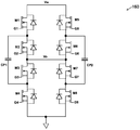
- FIG 2 illustrates a schematic diagram of a first implementation of the power converter shown in Figure 1 in accordance with various embodiments of the present disclosure.
- the power converter 160 is implemented as a two-phase 2: 1 switched capacitor power converter as shown in Figure 2.
- the two-phase 2: 1 switched capacitor power converter is alternatively referred to as the switched capacitor converter 160.
- the switched capacitor converter 160 comprises a first leg comprising four switches connected in series and a second leg comprising four switches connected in series.
- the first leg comprises a first switch M1, a second switch M2, a third switch M3 and a fourth switch M4 connected in series between an input power source VIN and ground.
- the fourth switch M4 is a low-side switch.
- Switches M1, M2 and M3 are high-side switches.
- the second leg comprises a fifth switch M5, a sixth switch M6, a seventh switch M7 and an eighth switch M8 connected in series between the input power source VIN and ground.
- the eighth switch M8 is a low-side switch.
- Switches M5, M6 and M7 are high-side switches.
- the switched capacitor converter 160 further comprises a first capacitor CP1 and a second capacitor CP2.
- the first capacitor CP1 is connected between a common node of switches M1 and M2, and a common node of switches M3 and M4.
- the second capacitor CP2 is connected between a common node of switches M5 and M6, and a common node of switches M7 and M8.
- the common node of switches M2 and M3 is connected to the common node of switches M6 and M7 as shown in Figure 2.
- the connection node of these two legs is the output of the switched capacitor converter 160 as shown in Figure 2.
- a shared bootstrap capacitor (not shown but illustrated in Figure 3) is configured to sequentially apply bias power to the high-side drivers of the high-side switches M1-M3 of the first leg and the high-side switches M5-M7 of the second leg.
- the switches of Figure 2 may be metal oxide semiconductor field-effect transistor (MOSFET) devices.
- the switching element can be any controllable switches such as insulated gate bipolar transistor (IGBT) devices, integrated gate commutated thyristor (IGCT) devices, gate turn-off thyristor (GTO) devices, silicon controlled rectifier (SCR) devices, junction gate field-effect transistor (JFET) devices, MOS controlled thyristor (MCT) devices and the like.
- IGBT insulated gate bipolar transistor
- IGCT integrated gate commutated thyristor
- GTO gate turn-off thyristor
- SCR silicon controlled rectifier
- JFET junction gate field-effect transistor
- MCT MOS controlled thyristor
- FIG. 2 shows the switches M1-M8 are implemented as single n-type transistors
- a person skilled in the art would recognize there may be many variations, modifications and alternatives.
- at least some of the switches M1-M8 may be implemented as p-type transistors.
- each switch shown in Figure 2 may be implemented as a plurality of switches connected in parallel.
- a capacitor may be connected in parallel with one switch to achieve zero voltage switching (ZVS) /zero current switching (ZCS) .
- each leg of the switched capacitor converter 160 operates in two different phases.
- a first phase the switches M1 and M3 of the first leg are turned on and switches M2 and M4 are turned off.
- the input power source VIN charges the first capacitor CP1.
- the switches M6 and M8 of the second leg are turned on and switches M5 and M7 are turned off.
- the energy stored in the second capacitor CP2 is discharged.
- the high-side switches M1, M3 and M6 are turned on in the first phase.
- the shared bootstrap capacitor (capacitor C0 shown in Figure 3) is applied sequentially to the high-side drivers of the switches M3, M6 and M1 in the first phase.
- the detailed operating principle and the control scheme of the shared bootstrap capacitor will be described below with respect to Figure 4.
- the switches M2 and M4 of the first leg are turned on and switches M1 and M3 are turned off.
- the energy stored in the first capacitor CP1 is discharged.
- the switches M5 and M7 of the second leg are turned on and switches M6 and M8 are turned off.
- the input power source VIN charges the second capacitor CP2.
- the high-side switches M2, M5 and M7 are turned on in the second phase.
- the shared bootstrap capacitor (capacitor C0 shown in Figure 3) is applied sequentially to the high-side drivers of the switches M7, M2 and M5 in the second phase.
- the detailed operating principle of the control scheme of the shared bootstrap capacitor will be described below with respect to Figure 4.
- FIG 3 illustrates a schematic diagram of the shared bootstrap capacitor and the associated control circuits in accordance with various embodiments of the present disclosure.
- the bootstrap capacitor 120 is implemented as a single capacitor C0 as shown in Figure 3.
- the bootstrap capacitor 120 is connected to a bias power supply V DRV through a first bias switch Sb1 and a second bias switch Sb2 as shown in Figure 3.
- the bias switches Sb1 and Sb2 are employed to control the process of charging the bootstrap capacitor 120.
- the detailed operating principle of the bias switches Sb1 and Sb2 will be described below with respect to Figure 4.
- the driver 150 comprises a first high-side driver block 151, a second high-side driver block 152, a third high-side driver block 153, a fifth high-side driver block 155, a sixth high-side driver block 156 and a seventh high-side driver block 157.
- the high-side driver blocks 151-153 and 155-157 are configured to drive the high-side switches M1-M3 and M5-M7 respectively.
- Each high-side driver block (e.g., the first high-side driver block 151) comprises an internal capacitor (e.g., capacitors C1-C7) and a drive circuit (e.g., drive circuits D1-D7) .
- the high-side drivers share the bootstrap capacitor 120.
- the bootstrap capacitor 120 may be alternatively referred to as the shared bootstrap capacitor 120.
- the bootstrap capacitor 120 may be alternatively referred to as the bootstrap capacitor C0.
- the shared bootstrap capacitor 120 provides bias power to establish a gate drive voltage higher than the source voltage of the high-side switch.
- the drive circuit may rely on the internal capacitor (e.g., capacitor C1) to completely turn off the high-side switch.
- the plurality of first switches 130 includes switches S11, S21, S31, S51, S61 and S71.
- the plurality of second switches 140 includes switches S12, S22, S32, S52, S62 and S72.
- Each high-side driver block (e.g., driver block 151) is connected to the shared bootstrap capacitor 120 through two switches.
- the bias terminals of the first high-side driver block 151 is connected to the shared bootstrap capacitor 120 through the switches S11 and S12 respectively.
- the shared bootstrap capacitor 120 is connected to the bias terminals of the first drive circuit D1 after the switches S11 and S12 have been turned on.
- the shared bootstrap capacitor 120 is disconnected from the bias terminals of the first drive circuit D1 after the switches S11 and S12 have been turned off.
- the first drive circuit D1 may rely on the internal capacitor C1 to maintain the operation.
- the switches S11-S71 and S12-S72 may be implemented as isolation switches. More particularly, each of the switches S11-S71 is implemented as two back-to-back connected p-channel transistors. Each of the switches S12-S72 is implemented as two back-to-back connected n-channel transistors. The detailed implementation of the isolation switches will be described below with respect to Figure 5.
- Figure 4 illustrates a timing diagram of the control mechanism applied to the shared bootstrap capacitor power converter system in accordance with various embodiments of the present disclosure.
- the horizontal axis of Figure 4 represents intervals of time. There may be thirteen vertical axes.
- the first vertical axis Y1 represents the turn-on time of the switches S61 and S62 (shown in Figure 3) .
- the second vertical axis Y2 represents the gate drive signal of the high-side switch M6 (shown in Figure 2) .
- the third vertical axis Y3 represents the turn-on time of the switches S31 and S32 (shown in Figure 3) .
- the fourth vertical axis Y4 represents the gate drive signal of the high-side switch M3 (shown in Figure 2) .
- the fifth vertical axis Y5 represents the turn-on time of the switches S11 and S12 (shown in Figure 3) .
- the sixth vertical axis Y6 represents the gate drive signal of the high-side switch M1 (shown in Figure 2) .
- the seventh vertical axis Y7 represents the turn-on time of the switches Sb1 and Sb2 (shown in Figure 3) .
- the eighth vertical axis Y8 represents the turn-on time of the switches S21 and S22 (shown in Figure 3) .
- the ninth vertical axis Y9 represents the gate drive signal of the high-side switch M2 (shown in Figure 2) .
- the tenth vertical axis Y10 represents the turn-on time of the switches S71 and S72 (shown in Figure 3) .
- the eleventh vertical axis Y11 represents the gate drive signal of the high-side switch M7 (shown in Figure 2) .
- the twelfth vertical axis Y12 represents the turn-on time of the switches S51 and S52 (shown in Figure 3) .
- the thirteenth vertical axis Y13 represents the gate drive signal of the high-side switch M5 (shown in Figure 2) .
- switches M1-M3 and M5-7 are high-side switches of the power converter 160.
- the power converter 160 operates in two different phases. As shown in Figure 4, during the time instant t0 to time instant t11, the power converter 160 operates in the first phase in which the first leg and the second leg are configured such that the first capacitor CP1 is charged and the second capacitor CP2 is discharged. During the first phase, the high-side switches M6, M3 and M1 are turned on as shown in Figure 4. During the time instant t11 to time instant t22, the power converter 160 operates in the second phase in which the first leg and the second leg are configured such that the first capacitor CP1 is discharged and the second capacitor CP2 is charged. During the second phase, the high-side switches M2, M7 and M5 are turned on as shown in Figure 4.
- the switches S61 and S62 have been turned on.
- the bootstrap capacitor 120 is connected to the bias terminal of the drive circuit D6.
- the bootstrap capacitor 120 is able to provide a bias voltage higher than the source voltage of the switch M6.
- the drive circuit D6 feeds a gate drive signal to the gate of the switch M6.
- the switch M6 is turned on and remains on until time instant t11 as shown in Figure 4.
- the switches S61 and S62 are turned off at time instant t3.
- the bootstrap capacitor 120 is disconnected from the drive circuit D6.
- the bootstrap capacitor 120 is ready to provide bias power for other high-side drivers.
- the turn-on process of the switch M3 (from t4 to t6) and the turn-on process of the switch M1 (from t7 to t9) are similar to that of the switch M6, and hence are not discussed herein to avoid repetition.
- the bias switches Sb1 and Sb2 are turned on at t10.
- the bias power source V DRV charges the bootstrap capacitor 120.
- the charging process of the bootstrap capacitor 120 extends from time instant t10 to time instant t11 as shown in Figure 4.
- the bias switches Sb1, Sb2 and the high-side switches M6, M3 and M1 are turned off simultaneously at time instant t11 as shown in Figure 4.
- the turn-on process of the high-side switch M2 (from t12 to t14)
- the turn-on process of the high-side switch M7 (from t15 to t17)
- the turn-on process of the high-side switch M5 (from t18 to t20) are similar to those of the first phase, and hence are discussed herein to avoid repetition.
- the bias switches Sb1 and Sb2 are turned on from time instant t21 to time instant t22.
- the bias power source V DRV charges the bootstrap capacitor 120.
- the charging process of the bootstrap capacitor 120 extends from time instant t21 to time instant t22 as shown in Figure 4.
- the bias switches Sb1, Sb2 and the high-side switches M2, M7 and M5 are turned off simultaneously at time instant t22 as shown in Figure 4.
- timing diagram shown in Figure 4 is merely an example, which should not unduly limit the scope of the claims.
- One of ordinary skill in the art would recognize many variations, alternatives, and modifications.
- the time delay between the turn-on of the switches S61/S62 and the turn-on of the switch M6 may vary depending on different applications and design needs.
- the timing for connecting the shared bootstrap capacitor to the high-side drivers may be different.
- Figure 4 illustrates the timing diagram of a power converter having six high-side switches operating in two different phases.
- This timing diagram is merely an example.
- the number of high-side switches can be different depending on applications and design needs. Furthermore, there may be a different number of phases, or a different number of high-side switches to be turned on in different phases.
- the control scheme shown in Figure 4 is applicable to a variety of applications. In certain applications, two or more external bootstrap capacitors may be shared by a plurality of high-side switches to improve the replenish time of the bootstrap capacitors. In these cases, the external capacitors may be replenished or switched to different internal capacitors at the same time.
- FIG 5 illustrates a schematic diagram of a first implementation of the drivers shown in Figure 1 in accordance with various embodiments of the present disclosure.
- the drive circuits of the high-side switches M1, M3, M3, M5, M6 and M7 are similar. For simplicity, only the drive circuit of the high-side switch M1 is discussed in detail herein.
- the detailed schematic diagrams of the drive circuits of the high-side switches M3, M3, M5, M6 and M7 are included in Figures 7-8 below.
- the high-side switch M1 is controlled by a high-side driver D1.
- the high-side driver D1 has two bias terminals connected to voltage potentials V DD1 and V SS1 respectively as shown in Figure 5.
- the high-side driver D1 is configured to receive a gate drive signal IN1.
- a controller (not shown) generates a control signal GC1 and feeds this control signal into the high-side driver D1 through a level shifter LS10 as shown in Figure 5.
- the level shifter LS10 has four bias terminals connected to voltage potentials V DRV , V DD1 , V SS1 and ground respectively as shown in Figure 5.
- the operating principle of level shifters is well known in the art, and hence is not discussed in further detail to avoid repetition.
- the high-side driver D1 and its associated circuit form the high-side driver block 151 as shown in Figure 5.
- a first isolation switch comprises a first p-type transistor S111 and a second p-type transistor S112.
- the first p-type transistor S111 and the second p-type transistor S112 are back-to-back connected to each other to form the first isolation switch.
- a second isolation switch comprises a first n-type transistor S121 and a second n-type transistor S122.
- the first n-type transistor S121 and the second n-type transistor S122 are back-to-back connected to each other to form the second isolation switch.
- the turn-on and turn-off of the first isolation switch and the second isolation switch are controlled by a plurality of level shifters and drivers.
- a controller (not shown) generates a control signal G11 for controlling the on/off of the first isolation switch and the second isolation switch.
- the control signal G11 is fed into level shifters LS11 and LS12 respectively.
- the outputs of the level shifters LS11 and LS12 are connected to the inputs of the drivers D11 and D12 respectively.
- drivers D11 and D12 have two outputs. The signals at the two outputs complement to each other as indicated by the dot at one output of the drivers.
- both the first isolation switch and the second isolation switch are turned on so that the external bootstrap capacitor C0 is connected to the bias terminals of the driver D1.
- the level shifters LS11/LS12, the drivers D11/D12 and the controller are configured such that both the first isolation switch and the second isolation switch are turned on and remain on during this time interval.
- the level shifters LS11/LS12, the drivers D11/D12 and the controller are configured such that both the first isolation switch and the second isolation switch are turned off and remain off.
- the level shifter LS11 is connected to voltage potentials V CAP+ and V CAP- .
- the level shifter LS11 is connected to voltage potentials V DD1 and V SS1 .
- the bootstrap capacitor C0 is connected to a bias power source V DRV through a first bias switch Sb1 and a second bias switch Sb2.
- the first bias switch Sb1 is implemented as a p-type transistor.
- the second bias switch Sb1 is implemented as an n-type transistor. As shown in Figure 5, the first bias switch Sb1, the second bias switch Sb2 and their associated drive circuits form an isolation switch block 161.
- both the first bias switch Sb1 and the second Sb2 switch are turned on so that the external bootstrap capacitor C0 is charged by the bias power source V DRV .
- the level shifter LS0, the drivers D01/D02 and the controller are configured such that both the first bias switch and the second bias switch are turned on and remain on during the time intervals.
- the level shifters LS11 and LS12 help to make the isolation switches operate correctly in two different voltage domains.
- the two voltage domains are the external bootstrap capacitor voltage domain indicated by V CAP+ /V CAP- and the internal capacitor voltage domain indicated by V DD1 /V SS1 .
- FIG. 6 illustrates a block diagram of a switched capacitor power converter system having a shared bootstrap capacitor in accordance with various embodiments of the present disclosure.
- the switched capacitor power converter system 600 comprises a switched capacitor power converter 160 and its associated drive circuits.
- the switched capacitor power converter 160 has been described above with respect to Figure 2, and hence is not discussed again herein.
- the switched capacitor power converter 160 comprises switches M1-M8.Switches M1-M3 and M5-7 are high-side switches.
- the high-side switches need a bootstrap capacitor to provide bias power.
- each high-side switch (e.g., switch M1) is driven by a high-side driver block (e.g., high-side driver block 151) .
- the high-side driver block is connected to the bootstrap capacitor 120 through an isolation switch block (e.g., isolation switch block 161) .
- All high-side driver blocks shown in Figure 6 share a same structure.
- the schematic diagram of the high-side driver block 151 has been discussed in detail above with respect to Figure 5, and hence the structures of the other high-side driver blocks 152, 153, 155, 156 and 157 are not discussed herein.
- all isolation switch blocks shown in Figure 6 share a same structure.
- the schematic diagram of the isolation switch block 161 has been discussed in detail above with respect to Figure 5, and hence the structures of the other isolation switch blocks 162, 163, 165, 166 and 167 are not discussed herein.
- the low-side switches M4 and M8 do not require a bootstrap capacitor. As shown in Figure 6, the low-side switch M4 is driven by the driver block 154. The low-side switch M8 is driven by the driver block 158. The bias power of the driver block 154 and the driver block 158 is from the bias power source V DRV directly.
- the power converter 160 includes a first leg comprising switches M1-M4 and the first capacitor CP1, and a second leg comprising switches M5-M8 and the second capacitor CP2.
- the first leg and the associated drive circuits are illustrated in detail below with respect to Figure 7.
- the second leg and the associated drive circuits are illustrated in detail below with respect to Figure 8.
- FIG. 7 illustrates a schematic diagram of a first half of the switched capacitor power converter in accordance with various embodiments of the present disclosure.
- switches M1-M4 are connected in series between the input power source VIN and ground.
- the drive circuit of the switch M1 has been described above with respect to Figure 5.
- the drive circuits of the switches M2 and M3 are similar to that of the switch M1, and hence are not discussed herein.
- the switch M4 is a low-side switch, which is driven by a low-side driver D4.
- the driver circuits of the switches M1, M2 and M3 share a same bootstrap capacitor C0.
- the bootstrap capacitor C0 is connected to the driver circuits D1, D2 and D3 of the switches M1, M2 and M3 in a controllable manner. More particularly, bootstrap capacitor C0 is connected to the driver circuits of the switches M1, M2 and M3 through turning on/off the isolation switches between the bootstrap capacitor C0 and the high-side drivers D1, D2 and D3.
- three level shifters L10, L20 and L30 are employed to convert the control signals GC1, GC2 and GC3 into suitable gate drive signals IN1, IN2 and IN3 for the high-side drivers D1, D2 and D3 as shown in Figure 7.
- FIG 8 illustrates a schematic diagram of a second half of the switched capacitor power converter in accordance with various embodiments of the present disclosure.
- switches M5-M8 are connected in series between the input power source VIN and ground.
- the drive circuits of switches M5-M8 are similar to the drive circuits of switches M1-M4 shown in Figure 7, and hence are not discussed again herein.
- FIG. 9 illustrates a block diagram of a control system applied to the switched capacitor power converter shown in Figure 1 in accordance with various embodiments of the present disclosure.
- the control system shown in Figure 9 has a reduced number of level shifters in comparison with that shown in Figures 7-8.
- a single level shifter is used for the V CAP+ /V CAP- domain to level shift the clock signal CLK.
- the timing of the control signals of the isolation switches (bi-directional switches) and the control signal of the bias switches are generated in the V CAP+ /V CAP- domain.
- a single level shifter e.g., LS911-LS971 is used in each driver capacitor domain V DDi /V SSi .
- the timing of the input signal of the high-side driver and the drive signal of the isolation switches are generated in the driver capacitor domain V DDi /V SSi .
- the phasing and timing of the turn-on sequence (e.g., GC1-GC8) may be implemented at the ground reference level as shown in Figure 9.
- the phasing and timing of the turn-on sequence (e.g., GC1-GC8) may be implemented at the driver capacitor domain.
- the control system comprises a level shifter 902, a pulse generator 904 and a phase/delay block 906. Both the level shifter 902 and the phase/delay block 906 are configured to receive a clock signal CLK.
- the clock signal CLK is fed into the pulse generator 904 through the level shifter 902.
- the pulse generator 904 is configured to generate control signals L12, L22, L32, L52, L62 and L72.
- L12 is the output signal of the level shifter LS12.
- L12 is used to control the on/off of the switches S111 and S121 through the driver D12.
- L22 is the output signal of the level shifter LS22.
- L22 is used to control the on/off of the switches S211 and S221 through the driver D22.
- L32 is the output signal of the level shifter LS32.
- L32 is used to control the on/off of the switches S311 and S321 through the driver D32.
- L52 is the output signal of the level shifter LS52.
- L52 is used to control the on/off of the switches S511 and S521 through the driver D52.
- L62 is the output signal of the level shifter LS62.
- L62 is used to control the on/off of the switches S611 and S621 through the driver D62.
- L72 is the output signal of the level shifter LS72. L72 is used to control the on/off of the switches S711 and S721 through the driver D72.
- the phase/delay block 906 is configured to generate control signals GC1, GC2, GC3, GC4, GC5, GC6, GC7 and GC8.
- GC4 and GC8 are used to control the low-side switches M4 and M8 of the power converter 160.
- GC4 is applied to the driver D4 directly.
- GC8 is applied to the driver D8 directly.
- the control signal GC1 passes through level shifter 911 and a pulse/delay block 912.
- the pulse/delay block 912 generates control signals L11 and IN1.
- L11 is the output signal of the level shifter LS11.
- L11 is used to control the on/off of the switches S112 and S122 through the driver D11.
- IN1 is fed into the drive D1 to control the switch M1.
- the control signal GC2 passes through level shifter 921 and a pulse/delay block 922.
- the pulse/delay block 922 generates control signals L21 and IN2.
- L21 is the output signal of the level shifter LS21.
- L21 is used to control the on/off of the switches S212 and S222 through the driver D21.
- IN2 is fed into the drive D2 to control the switch M2.
- the control signal GC3 passes through level shifter 931 and a pulse/delay block 932.
- the pulse/delay block 932 generates control signals L31 and IN3.
- L31 is the output signal of the level shifter LS31.
- L31 is used to control the on/off of the switches S312 and S322 through the driver D31.
- IN3 is fed into the drive D3 to control the switch M3.
- the control signal GC5 passes through level shifter 951 and a pulse/delay block 952.
- the pulse/delay block 952 generates control signals L51 and IN5.
- L51 is the output signal of the level shifter LS51.
- L51 is used to control the on/off of the switches S512 and S522 through the driver D51.
- IN5 is fed into the drive D5 to control the switch M5.
- the control signal GC6 passes through level shifter 961 and a pulse/delay block 962.
- the pulse/delay block 962 generates control signals L61 and IN6.
- L61 is the output signal of the level shifter LS61. L61 is used to control the on/off of the switches S612 and S622 through the driver D61. IN6 is fed into the drive D6 to control the switch M6.
- the control signal GC7 passes through level shifter 971 and a pulse/delay block 972.
- the pulse/delay block 972 generates control signals L71 and IN7.
- L71 is the output signal of the level shifter LS71. L71 is used to control the on/off of the switches S712 and S722 through the driver D71. IN7 is fed into the drive D7 to control the switch M7.
- FIG 10 illustrates a schematic diagram of a second implementation of the drivers shown in Figure 1 in accordance with various embodiments of the present disclosure.
- the drivers shown in Figure 10 are similar to the drivers shown in Figure 5 except that two p-type transistors S111 and S112 are controlled by a same driver D11, and two n-type transistors S121 and S122 are controlled by a same driver D12.
- a first diode D111 and a second diode D112 are back-to-back connected to each other.
- the back-to-back connected D111 and D112 are connected in parallel with the back-to-back connected S121 and S122.
- the common node of D111 and D112 is denoted as V SS1_MAX .
- the common node of S121 and S122 is denoted as V SS1_MIN .
- a third diode D121 and a fourth diode D122 are back-to-back connected to each other.
- the back-to-back connected D121 and D122 are connected in parallel with the back-to-back connected S111 and S112.
- the common node of D121 and D122 is denoted as V DD1_MIN .
- the common node of S111 and S112 is denoted as V DD1_MAX .
- the diodes D111, D112, D121 and D122 are added to provide proper rails for the drivers D11 and D12.
- the level shifter LS11 has four bias terminals connected to voltage potentials V DD1_MAX , V DRV , V SS1_MAX and ground respectively.
- the output signal of the level shifter LS11 is fed into the driver D11.
- the driver D11 has two bias terminals connected to voltage potentials V SS1_MAX and V DD1_MAX respectively.
- the output signal of the driver D11 is used to drive both S111 and S112 as shown in Figure 10.
- the level shifter LS12 has four bias terminals connected to voltage potentials V DD1_MIN , V DRV , V SS1_MIN and ground respectively.
- the output signal of the level shifter LS12 is fed into the driver D12.
- the driver D12 has two bias terminals connected to voltage potentials V SS1_MIN and V DD1_MIN respectively.
- the output signal of the driver D12 is used to drive both S121 and S122 as shown in Figure 10.
- back-to-back connected p-type transistors S111 and S112 have the same gate control signal. Such a configuration helps to simplify the control of the isolation switch so as to improve the performance of the power converter 160.
- the back-to-back connected n-type transistors S121 and S122 have the same gate control signal as shown in Figure 10.
- FIG 11 illustrates a block diagram of a switched capacitor power converter having a shared bootstrap capacitor and the drivers shown in Figure 10 in accordance with various embodiments of the present disclosure.
- the switched capacitor power converter system 1100 is similar to the switched capacitor power converter system 600 shown in Figure 6 except that the isolation switches 181, 182, 183, 185, 186 and 187 comprise the drive circuit shown in Figure 10.
- Figure 12 illustrates a flow chart of a method for controlling the shared bootstrap capacitor power converter shown in Figure 1 in accordance with various embodiments of the present disclosure.
- This flowchart shown in Figure 12 is merely an example, which should not unduly limit the scope of the claims.
- One of ordinary skill in the art would recognize many variations, alternatives, and modifications. For example, various steps illustrated in Figure 12 may be added, removed, replaced, rearranged and repeated.
- a switched capacitor power converter comprises a plurality of high-side switches and one shared bootstrap capacitor. Each of the plurality of high-side switches is driven by a high-side driver.
- the high-side driver has two bias terminals connected to two terminals of the shared bootstrap capacitor through two isolation switches respectively.
- the switched capacitor power converter operates in two different phases, namely a charge phase and a discharge phase.
- the bootstrap capacitor is connected to a first high-side driver through turning on a first isolation switch and a second isolation switch.
- the first isolation switch is connected between a positive bias terminal of the first high-side driver and a positive terminal of the bootstrap capacitor.
- the second isolation switch is connected between a negative bias terminal of the first high-side driver and a negative terminal of the bootstrap capacitor.
- the first high-side driver applies a gate drive signal to the first high-side switch.
- the first high-side switch is turned on.
- the delay may be in a range from about 50 nanoseconds to about 100 nanoseconds. The range is merely an example. Depending on different applications and design needs, the range above may vary accordingly.
- the bootstrap capacitor is disconnected from the first high-side driver through turning off the first isolation switch and the second isolation switch. There is a delay between the turn-on of the first high-side switch and disconnecting the bootstrap capacitor from the first high-side driver.
- the delay may be in a range from about 50 nanoseconds to about 100 nanoseconds. The range is merely an example. Depending on different applications and design needs, the range above may vary accordingly.
- the bootstrap capacitor is connected to a second high-side driver through turning on a third isolation switch and a fourth isolation switch.
- the third isolation switch is connected between a positive bias terminal of the second high-side driver and the positive terminal of the bootstrap capacitor.
- the fourth isolation switch is connected between a negative bias terminal of the second high-side driver and the negative terminal of the bootstrap capacitor.
- the second high-side driver applies a gate drive signal to the second high-side switch.
- the second high-side switch is turned on.
- the delay may be in a range from about 50 nanoseconds to about 100 nanoseconds. The range is merely an example. Depending on different applications and design needs, the range above may vary accordingly.
- the bootstrap capacitor is disconnected from the second high-side driver through turning off the third isolation switch and the fourth isolation switch. There is a delay between the turn-on of the second high-side switch and disconnecting the bootstrap capacitor from the second high-side driver.
- the delay may be in a range from about 50 nanoseconds to about 100 nanoseconds. The range is merely an example. Depending on different applications and design needs, the range above may vary accordingly.
- the bootstrap capacitor is disconnected from all high-side drivers.
- the bias switches connected between the bootstrap capacitor and a bias power source are turned on.
- the bias power source charges the bootstrap capacitor.
- the high-side switches and bias switches are turned off simultaneously.
- the bootstrap capacitor is disconnected from all high-side drivers.
- the bias switches connected between the bootstrap capacitor and the bias power source are turned on.
- the bias power source charges the bootstrap capacitor.
- the high-side switches and bias switches are turned off simultaneously.
- FIG 13 illustrates a schematic diagram of a second implementation of the power converter shown in Figure 1 in accordance with various embodiments of the present disclosure.
- the switched capacitor power converter 160 shown in Figure 13 is a single phase 2: 1 switched capacitor power converter. As shown in Figure 13, switches M1, M2, M3 and M4 are connected in series between the input power source VIN and ground.
- the operating principle of the switched capacitor power converter 160 is similar to that shown in Figure 2, and hence is not discussed herein in detail to avoid repetition.
- switches M1, M2 and M3 are high-side switches.
- the drive circuits of M2 and M3 are similar to that shown in Figure 5.
- the drive circuit of the first high-side switch M1 is different and will be described in detail below with respect to Figure 14.
- Figure 14 illustrates a schematic diagram of the drive circuit of the first high-side switch shown in Figure 13 in accordance with various embodiments of the present disclosure.
- the schematic diagram of the drive circuit of the first high-side switch M1 shown in Figure 14 is similar to the drive circuit shown in Figure 5 except that the isolation switch shown in Figure 5 has been replaced by a single transistor. More particularly, the isolation switch between the positive bias terminal of D1 and the external bootstrap capacitor C0 is replaced by a p-type transistor S112 as shown in Figure 14. Moreover, the isolation switch between the negative bias terminal of D1 and the external bootstrap capacitor C0 is replaced by an n-type transistor S121 as shown in Figure 14.
- the source of the first high-side switch M1 has the highest voltage potential in comparison with the sources of the switches M2 and M3. As a result, it is possible to use the drive circuit shown in Figure 14 to drive the first high-side switch M1.
- One advantageous feature of having the drive circuit shown in Figure 14 is the simplified drive circuit helps to reduce the cost of the driver circuit and improve the reliability of the power converter 160.
- Figure 15 illustrates a schematic diagram of the drive circuits of the switched capacitor power converter shown in Figure 13 in accordance with various embodiments of the present disclosure.
- the schematic diagram of the drive circuits shown in Figure 15 is similar to that shown in Figure 7 except that the first high-side switch M1 has a simplified drive circuit as described above with respect to Figure 14.
- an apparatus comprising a first high-side gate driver means configured to drive a first high-side switch, a second high-side gate driver means configured to drive a second high-side switch, and a bootstrap capacitor means configured to provide bias power for the first high-side gate driver and the second high-side gate driver through a first group of isolation switches and a second group of isolation switches respectively.
Landscapes
- Engineering & Computer Science (AREA)
- Power Engineering (AREA)
- Power Conversion In General (AREA)
Abstract
A system comprises a switched capacitor power converter comprising a first leg comprising four switches connected in series and a second leg comprising four switches connected in series and a shared bootstrap capacitor configured to sequentially apply bias power to high-side switches of the first leg and the second leg.
Description
The present disclosure relates to a power converter having a shared bootstrap capacitor, and, in particular embodiments, to a shared bootstrap capacitor employed in a switched capacitor power converter.
As technologies further advance, a variety of electronic devices, such as mobile phones, tablet PCs, digital cameras, MP3 players and/or the like, have become popular. Each electronic device requires direct current power at a substantially constant voltage which may be regulated within a specified tolerance even when the current drawn by the electronic device may vary over a wide range. In order to maintain the voltage within the specified tolerance, power converters (e.g., switching dc/dc converters) coupled to the electronic device are capable of providing very fast transient responses, while keeping a stable output voltage under various load transients.
Many power converters (e.g., switching dc/dc converters) include two n-type switches (e.g., power MOSFETs) connected in series between an input power source and ground. The switch connected to the input power source is commonly known as a high-side switch, and the switch connected to ground is commonly known as a low-side switch. A low-side driver circuit and a high-side drive circuit are employed to control the gates of the low-side switch and the high-side switch respectively. The bias power of the low-side driver circuit is supplied from a regulated bias voltage. In order to turn on the high-side switch (e.g., n-type high-side switches) , the high-side drive circuit may need a gate voltage higher than the voltage of the input power source.
A bootstrap circuit may generate a gate voltage higher than the voltage of the input power source. The bootstrap circuit comprises a switch, a bootstrap capacitor and a bootstrap diode. The switch may be implemented as the low-side switch. The bootstrap diode is connected between a bias power source and a positive terminal of the bootstrap capacitor. More particularly, the anode of the bootstrap diode is connected to the bias power source and the cathode of the bootstrap diode is connected to the bootstrap capacitor. The negative terminal of the bootstrap capacitor is connected to the common node of the high-switch and the low-side switch.
In operation, after the low-side switch is turned on, the bias power source charges the bootstrap capacitor through a conductive channel formed by the bootstrap diode and the low-side switch. After the low-side switch is turned off and the high-side switch is turned on, the negative terminal of the bootstrap capacitor is pulled up to the voltage of the input power source. The bootstrap diode becomes reverse biased and the bootstrap capacitor functions as a floating power supply for driving the high-side switch. More particularly, a voltage equal to the voltage of the input power source plus the voltage of the bias power source is used to drive the gate of the high-side switch.
As power electronics technologies evolve, multilevel power converters have emerged as an effective alternative to further reduce voltage stresses of semiconductor devices. In a multilevel power converter (e.g., a switched capacitor power converter) , there may be a plurality of high-side switches connected in series. Each high-side switch needs a high-side driver. In order to generate a voltage higher enough to drive the corresponding high-side switch, each high-side driver needs a bootstrap capacitor. As such, the multilevel power converter may need a plurality of bootstrap capacitors. The plurality of bootstrap capacitors is normally implemented as external discrete capacitors.
In some applications with space constraints such as cell phone applications, it would be desirable to have a shared bootstrap capacitor capable of driving the plurality of high-side switches under a variety of operating conditions.
SUMMARY
These and other problems are generally solved or circumvented, and technical advantages are generally achieved, by preferred embodiments of the present disclosure which provide a shared bootstrap capacitor for improving the performance of switched capacitor power converter systems.
In accordance with an embodiment, an apparatus comprises a first high-side gate driver, a second high-side gate driver and a bootstrap capacitor. The first high-side gate driver is configured to drive a first high-side switch. The second high-side gate driver is configured to drive a second high-side switch. The bootstrap capacitor is configured to provide bias power for the first high-side gate driver and the second high-side gate driver through a first group of isolation switches and a second group of isolation switches respectively.
A first terminal of the bootstrap capacitor is connected to a first bias power input of the first high-side gate driver through a first isolation switch. A second terminal of the bootstrap capacitor is connected to a second bias power input of the first high-side gate driver through a second isolation switch. The first isolation switch comprises a first p-type transistor and a second p-type transistor back-to-back connected to each other. The second isolation switch comprises a first n-type transistor and a second n-type transistor back-to-back connected to each other.
Alternatively, the first terminal of the bootstrap capacitor is connected to a first bias power input of the first high-side gate driver through two back-to-back connected first transistors and two back-to-back connected first diodes. The two back-to-back connected first transistors and the two back-to-back connected first diodes are connected in parallel. The second terminal of the bootstrap capacitor is connected to a second bias power input of the first high-side gate driver through two back-to-back connected second transistors and two back-to-back connected second diodes. The two back-to-back connected second transistors and the two back-to-back connected second diodes are connected in parallel
In accordance with another embodiment, a method comprises connecting a bootstrap capacitor to a first high-side driver through turning on first isolation switches between the bootstrap capacitor and the first high-side driver. The method further comprises turning on a first high-side switch and after turning on the first high-side switch and disconnecting the bootstrap capacitor from the first high-side driver by turning off the first isolation switches. The method further comprises connecting the bootstrap capacitor to a second high-side driver through turning on second isolation switches between the bootstrap capacitor and the second high-side driver and turning on a second high-side switch and after turning on the second high-side switch and disconnecting the bootstrap capacitor from the second high-side driver by turning off the second isolation switches.
The method further comprises charging the bootstrap capacitor through turning on switches between a bias voltage source and the bootstrap capacitor, and charging the bootstrap capacitor after both the first high-side switch and the second high-side switch are fully turned on.
The bootstrap capacitor is shared by a plurality of high-side switches of a switched capacitor power converter. The bootstrap capacitor is sequentially connected to the plurality of high-side switches of the switched capacitor power converter.
In accordance with yet another embodiment, a system comprises a switched capacitor power converter comprising a first leg comprising four switches connected in series and a second leg comprising four switches connected in series and a shared bootstrap capacitor configured to sequentially apply bias power to high-side switches of the first leg and the second leg.
The first leg comprises a first switch, a second switch, a third switch and a fourth switch connected in series between a power source and ground. The second leg comprises a fifth switch, a sixth switch, a seventh switch and an eighth switch connected in series between the power source and ground. A first capacitor connected between a common node of the first switch and the second switch, and a common node of the third switch and the fourth switch. A second capacitor connected between a common node of the fifth switch and the sixth switch, and a common node of the seventh switch and the eighth switch.
A first driver is configured to drive the first switch, and wherein the shared bootstrap capacitor is connected to the first driver through a first isolation switch and a second isolation switch. The first isolation switch and the second isolation switch are configured to be turned on simultaneously before turning on the first switch. The shared bootstrap capacitor is connected to a bias power supply through a first bias switch and a second bias switch. The first bias switch and the second bias switch are configured to be turned on after the first switch is turned on. The first bias switch, the second bias switch and the first switch are configured to be turned off simultaneously.
An advantage of an embodiment of the present disclosure is employing a shared bootstrap capacitor in a switched capacitor power converter so as to improve the efficiency, reliability and cost of the switched capacitor power converter.
The foregoing has outlined rather broadly the features and technical advantages of the present disclosure in order that the detailed description of the disclosure that follows may be better understood. Additional features and advantages of the disclosure will be described hereinafter which form the subject of the claims of the disclosure. It should be appreciated by those skilled in the art that the conception and specific embodiment disclosed may be readily utilized as a basis for modifying or designing other structures or processes for carrying out the same purposes of the present disclosure. It should also be realized by those skilled in the art that such equivalent constructions do not depart from the spirit and scope of the disclosure as set forth in the appended claims.
For a more complete understanding of the present disclosure, and the advantages thereof, reference is now made to the following descriptions taken in conjunction with the accompanying drawings, in which:
Figure 1 illustrates a block diagram of a shared bootstrap capacitor power converter system in accordance with various embodiments of the present disclosure;
Figure 2 illustrates a schematic diagram of a first implementation of the power converter shown in Figure 1 in accordance with various embodiments of the present disclosure;
Figure 3 illustrates a schematic diagram of the shared bootstrap capacitor and the associated control circuits in accordance with various embodiments of the present disclosure;
Figure 4 illustrates a timing diagram of the control mechanism applied to the shared bootstrap capacitor power converter system in accordance with various embodiments of the present disclosure;
Figure 5 illustrates a schematic diagram of a first implementation of the drivers shown in Figure 1 in accordance with various embodiments of the present disclosure;
Figure 6 illustrates a block diagram of a switched capacitor power converter having a shared bootstrap capacitor in accordance with various embodiments of the present disclosure;
Figure 7 illustrates a schematic diagram of a first half of the switched capacitor power converter in accordance with various embodiments of the present disclosure;
Figure 8 illustrates a schematic diagram of a second half of the switched capacitor power converter in accordance with various embodiments of the present disclosure;
Figure 9 illustrates a block diagram of a control system applied to the switched capacitor power converter shown in Figure 1 in accordance with various embodiments of the present disclosure;
Figure 10 illustrates a schematic diagram of a second implementation of the drivers shown in Figure 1 in accordance with various embodiments of the present disclosure;
Figure 11 illustrates a block diagram of a switched capacitor power converter having a shared bootstrap capacitor and the drivers shown in Figure 10 in accordance with various embodiments of the present disclosure;
Figure 12 illustrates a flow chart of a method for controlling the shared bootstrap capacitor power converter shown in Figure 1 in accordance with various embodiments of the present disclosure;
Figure 13 illustrates a schematic diagram of a second implementation of the power converter shown in Figure 1 in accordance with various embodiments of the present disclosure;
Figure 14 illustrates a schematic diagram of the drive circuit of the first high-side switch shown in Figure 13 in accordance with various embodiments of the present disclosure; and
Figure 15 illustrates a schematic diagram of the drive circuits of the switched capacitor power converter shown in Figure 13 in accordance with various embodiments of the present disclosure.
Corresponding numerals and symbols in the different figures generally refer to corresponding parts unless otherwise indicated. The figures are drawn to clearly illustrate the relevant aspects of the various embodiments and are not necessarily drawn to scale.
DETAILED DESCRIPTION OF ILLUSTRATIVE EMBODIMENTS
The making and using of the presently preferred embodiments are discussed in detail below. It should be appreciated, however, that the present disclosure provides many applicable inventive concepts that can be embodied in a wide variety of specific contexts. The specific embodiments discussed are merely illustrative of specific ways to make and use the disclosure, and do not limit the scope of the disclosure.
The present disclosure will be described with respect to preferred embodiments in a specific context, namely a switched capacitor power converter having a shared bootstrap capacitor. The present disclosure may also be applied, however, to a variety of power converters having multiple high-side switches. Hereinafter, various embodiments will be explained in detail with reference to the accompanying drawings.
Figure 1 illustrates a block diagram of a shared bootstrap capacitor power converter system in accordance with various embodiments of the present disclosure. The shared bootstrap capacitor power converter system 100 comprises a power converter 160, a plurality of drivers 150, a plurality of first switches 130, a plurality of second switches 140, a bootstrap capacitor 120 and a controllable bias circuit 110.
As shown in Figure 1, the controllable bias circuit 110 is connected to the bootstrap capacitor 120. In some embodiments, the controllable bias circuit 110 is employed to maintain the voltage across the bootstrap capacitor. In particular, the controllable bias circuit 110 may comprise a bias power source and two bias switches connected between the bias power source and the bootstrap capacitor 120. When replenishing the bootstrap capacitor 120 is necessary, the bootstrap capacitor 120 is connected to the bias power source and charged by the bias power source after the two bias switches have been turned on. On the other hand, the bootstrap capacitor 120 is disconnected from the bias power source by turning off the two bias switches. The detailed schematic diagram of the controllable bias circuit 110 will be described below with respect to Figures 3 and 5.
In some embodiments, the bootstrap capacitor 120 may be implemented as a single external capacitor shared by a plurality of high-side drivers (e.g., drivers 150) . Alternatively, the bootstrap capacitor 120 may comprise a plurality of discrete capacitors shared by a plurality of high-side drivers (e.g., drivers 150) . The number of the plurality of discrete capacitors is less than the number the plurality of high-side drivers. For example, the power converter 160 may comprise two phases. Each phase comprises three high-side switches. The drivers 150 may comprise six high-side drivers for driving their respective high-side switches of the two phases. The bootstrap capacitor 120 comprises two discrete capacitors. A first discrete capacitor functions as a first bootstrap capacitor shared by the high-side drivers of the first phase. A second discrete capacitor functions as a second bootstrap capacitor shared by the high-side drivers of the second phase.
It should be noted that the number of the discrete capacitors used in the previous example is selected purely for demonstration purposes and is not intended to limit the various embodiments of the present disclosure to any particular number of the discrete capacitors.
It should further be noted that in the example above, allocating the two discrete capacitors to two different phases is merely an example. Depending on different applications and design needs, the allocation of the discrete capacitors may vary accordingly. For example, the first discrete capacitor above may be implemented as an external capacitor. The second discrete capacitor above may be implemented as an internal capacitor embedded in the chip where the drivers are located. The first discrete capacitor functions as a first bootstrap capacitor shared by four high-side drivers. The second discrete capacitor functions as a second bootstrap capacitor shared by two high-side drivers.
The bootstrap capacitor 120 is connected to the drivers 150 through the plurality of first switches 130 and the plurality of second switches 140. The drivers 150 may comprise a plurality of high-side drivers configured to drive the respective high-side switches of the power converter 160. Both the plurality of first switches 130 and the plurality of second switches 140 comprise a plurality of isolation switches. In some embodiments, by controlling the on/off of the plurality of isolation switches, the bootstrap capacitor 120 may be connected to or disconnected from the plurality of high-side drivers sequentially. The detailed schematic diagram and operation principle of the switches 130 and 140 will be described below with respect to Figures 3-4.
The power converter 160 comprises a plurality of high-side switches driven by the high-side drivers of the drivers 150. In some embodiments, the power converter 160 may be a non-isolated power converter such as a charge pump power converter, a two-phase switched capacitor power converter, a multiphase buck converter, any combinations thereof and the like. In alternative embodiments, the power converter 160 may be an isolated power converter such as a dual full-bridge power converter, a dual half-bridge half converter, a dual LLC power converter, any combinations thereof and the like. In an embodiment, the power converter 160 is implemented as a two-phase 2: 1 switched capacitor power converter. The schematic diagram of the two-phase 2: 1 switched capacitor power converter will be described below with respect to Figure 2.
Figure 2 illustrates a schematic diagram of a first implementation of the power converter shown in Figure 1 in accordance with various embodiments of the present disclosure. In some embodiments, the power converter 160 is implemented as a two-phase 2: 1 switched capacitor power converter as shown in Figure 2. For simplicity, throughout the description, the two-phase 2: 1 switched capacitor power converter is alternatively referred to as the switched capacitor converter 160. The switched capacitor converter 160 comprises a first leg comprising four switches connected in series and a second leg comprising four switches connected in series.
As shown in Figure 2, the first leg comprises a first switch M1, a second switch M2, a third switch M3 and a fourth switch M4 connected in series between an input power source VIN and ground. As well known in the art, the fourth switch M4 is a low-side switch. Switches M1, M2 and M3 are high-side switches. The second leg comprises a fifth switch M5, a sixth switch M6, a seventh switch M7 and an eighth switch M8 connected in series between the input power source VIN and ground. As well known in the art, the eighth switch M8 is a low-side switch. Switches M5, M6 and M7 are high-side switches.
The switched capacitor converter 160 further comprises a first capacitor CP1 and a second capacitor CP2. The first capacitor CP1 is connected between a common node of switches M1 and M2, and a common node of switches M3 and M4. The second capacitor CP2 is connected between a common node of switches M5 and M6, and a common node of switches M7 and M8. The common node of switches M2 and M3 is connected to the common node of switches M6 and M7 as shown in Figure 2. The connection node of these two legs is the output of the switched capacitor converter 160 as shown in Figure 2.
In some embodiments, a shared bootstrap capacitor (not shown but illustrated in Figure 3) is configured to sequentially apply bias power to the high-side drivers of the high-side switches M1-M3 of the first leg and the high-side switches M5-M7 of the second leg.
In accordance with an embodiment, the switches of Figure 2 (e.g., switches M1-M8) may be metal oxide semiconductor field-effect transistor (MOSFET) devices. Alternatively, the switching element can be any controllable switches such as insulated gate bipolar transistor (IGBT) devices, integrated gate commutated thyristor (IGCT) devices, gate turn-off thyristor (GTO) devices, silicon controlled rectifier (SCR) devices, junction gate field-effect transistor (JFET) devices, MOS controlled thyristor (MCT) devices and the like.
It should be noted while Figure 2 shows the switches M1-M8 are implemented as single n-type transistors, a person skilled in the art would recognize there may be many variations, modifications and alternatives. For example, depending on different applications and design needs, at least some of the switches M1-M8 may be implemented as p-type transistors. Furthermore, each switch shown in Figure 2 may be implemented as a plurality of switches connected in parallel. Moreover, a capacitor may be connected in parallel with one switch to achieve zero voltage switching (ZVS) /zero current switching (ZCS) .
In operation, each leg of the switched capacitor converter 160 operates in two different phases. In a first phase, the switches M1 and M3 of the first leg are turned on and switches M2 and M4 are turned off. As a result of turning on M1 and M3, the input power source VIN charges the first capacitor CP1. Also in the first phase, the switches M6 and M8 of the second leg are turned on and switches M5 and M7 are turned off. As a result of turning on M6 and M8, the energy stored in the second capacitor CP2 is discharged. In sum, the high-side switches M1, M3 and M6 are turned on in the first phase.
In some embodiments, the shared bootstrap capacitor (capacitor C0 shown in Figure 3) is applied sequentially to the high-side drivers of the switches M3, M6 and M1 in the first phase. The detailed operating principle and the control scheme of the shared bootstrap capacitor will be described below with respect to Figure 4.
In a second phase, the switches M2 and M4 of the first leg are turned on and switches M1 and M3 are turned off. As a result of turning on M2 and M4, the energy stored in the first capacitor CP1 is discharged. Also in the second phase, the switches M5 and M7 of the second leg are turned on and switches M6 and M8 are turned off. As a result of turning on M5 and M7, the input power source VIN charges the second capacitor CP2. In sum, the high-side switches M2, M5 and M7 are turned on in the second phase.
In some embodiments, the shared bootstrap capacitor (capacitor C0 shown in Figure 3) is applied sequentially to the high-side drivers of the switches M7, M2 and M5 in the second phase. The detailed operating principle of the control scheme of the shared bootstrap capacitor will be described below with respect to Figure 4.
Figure 3 illustrates a schematic diagram of the shared bootstrap capacitor and the associated control circuits in accordance with various embodiments of the present disclosure. The bootstrap capacitor 120 is implemented as a single capacitor C0 as shown in Figure 3. The bootstrap capacitor 120 is connected to a bias power supply V
DRV through a first bias switch Sb1 and a second bias switch Sb2 as shown in Figure 3. The bias switches Sb1 and Sb2 are employed to control the process of charging the bootstrap capacitor 120. The detailed operating principle of the bias switches Sb1 and Sb2 will be described below with respect to Figure 4.
The driver 150 comprises a first high-side driver block 151, a second high-side driver block 152, a third high-side driver block 153, a fifth high-side driver block 155, a sixth high-side driver block 156 and a seventh high-side driver block 157. The high-side driver blocks 151-153 and 155-157 are configured to drive the high-side switches M1-M3 and M5-M7 respectively. Each high-side driver block (e.g., the first high-side driver block 151) comprises an internal capacitor (e.g., capacitors C1-C7) and a drive circuit (e.g., drive circuits D1-D7) .
As shown in Figure 3, the high-side drivers share the bootstrap capacitor 120. Throughout the description, the bootstrap capacitor 120 may be alternatively referred to as the shared bootstrap capacitor 120. Moreover, the bootstrap capacitor 120 may be alternatively referred to as the bootstrap capacitor C0.
During the turn-on process of a high-side switch, the shared bootstrap capacitor 120 provides bias power to establish a gate drive voltage higher than the source voltage of the high-side switch. During the turn-off process of the high-side switch, the drive circuit may rely on the internal capacitor (e.g., capacitor C1) to completely turn off the high-side switch.
As shown in Figure 3, the plurality of first switches 130 includes switches S11, S21, S31, S51, S61 and S71. The plurality of second switches 140 includes switches S12, S22, S32, S52, S62 and S72. Each high-side driver block (e.g., driver block 151) is connected to the shared bootstrap capacitor 120 through two switches. For example, the bias terminals of the first high-side driver block 151 is connected to the shared bootstrap capacitor 120 through the switches S11 and S12 respectively.
In operation, the shared bootstrap capacitor 120 is connected to the bias terminals of the first drive circuit D1 after the switches S11 and S12 have been turned on. On the other hand, the shared bootstrap capacitor 120 is disconnected from the bias terminals of the first drive circuit D1 after the switches S11 and S12 have been turned off. After the shared bootstrap capacitor 120 is disconnected from the bias terminals of the first drive circuit D1, the first drive circuit D1 may rely on the internal capacitor C1 to maintain the operation.
The switches S11-S71 and S12-S72 may be implemented as isolation switches. More particularly, each of the switches S11-S71 is implemented as two back-to-back connected p-channel transistors. Each of the switches S12-S72 is implemented as two back-to-back connected n-channel transistors. The detailed implementation of the isolation switches will be described below with respect to Figure 5.
Figure 4 illustrates a timing diagram of the control mechanism applied to the shared bootstrap capacitor power converter system in accordance with various embodiments of the present disclosure. The horizontal axis of Figure 4 represents intervals of time. There may be thirteen vertical axes. The first vertical axis Y1 represents the turn-on time of the switches S61 and S62 (shown in Figure 3) . The second vertical axis Y2 represents the gate drive signal of the high-side switch M6 (shown in Figure 2) . The third vertical axis Y3 represents the turn-on time of the switches S31 and S32 (shown in Figure 3) . The fourth vertical axis Y4 represents the gate drive signal of the high-side switch M3 (shown in Figure 2) . The fifth vertical axis Y5 represents the turn-on time of the switches S11 and S12 (shown in Figure 3) . The sixth vertical axis Y6 represents the gate drive signal of the high-side switch M1 (shown in Figure 2) . The seventh vertical axis Y7 represents the turn-on time of the switches Sb1 and Sb2 (shown in Figure 3) .
The eighth vertical axis Y8 represents the turn-on time of the switches S21 and S22 (shown in Figure 3) . The ninth vertical axis Y9 represents the gate drive signal of the high-side switch M2 (shown in Figure 2) . The tenth vertical axis Y10 represents the turn-on time of the switches S71 and S72 (shown in Figure 3) . The eleventh vertical axis Y11 represents the gate drive signal of the high-side switch M7 (shown in Figure 2) . The twelfth vertical axis Y12 represents the turn-on time of the switches S51 and S52 (shown in Figure 3) . The thirteenth vertical axis Y13 represents the gate drive signal of the high-side switch M5 (shown in Figure 2) .
Referring back to Figure 2, switches M1-M3 and M5-7 are high-side switches of the power converter 160. As described above with respect to Figure 2, the power converter 160 operates in two different phases. As shown in Figure 4, during the time instant t0 to time instant t11, the power converter 160 operates in the first phase in which the first leg and the second leg are configured such that the first capacitor CP1 is charged and the second capacitor CP2 is discharged. During the first phase, the high-side switches M6, M3 and M1 are turned on as shown in Figure 4. During the time instant t11 to time instant t22, the power converter 160 operates in the second phase in which the first leg and the second leg are configured such that the first capacitor CP1 is discharged and the second capacitor CP2 is charged. During the second phase, the high-side switches M2, M7 and M5 are turned on as shown in Figure 4.
At time instant t1, the switches S61 and S62 have been turned on. Referring back to Figure 3, in response to the turn-on of the switches S61 and S62, the bootstrap capacitor 120 is connected to the bias terminal of the drive circuit D6. The bootstrap capacitor 120 is able to provide a bias voltage higher than the source voltage of the switch M6. At time instant t2, the drive circuit D6 feeds a gate drive signal to the gate of the switch M6. In response to the gate drive signal from the drive circuit D6, the switch M6 is turned on and remains on until time instant t11 as shown in Figure 4. After the switch M6 has been turned on, the switches S61 and S62 are turned off at time instant t3. In response to the turn-off of the switches S61 and S62, the bootstrap capacitor 120 is disconnected from the drive circuit D6. The bootstrap capacitor 120 is ready to provide bias power for other high-side drivers.
The turn-on process of the switch M3 (from t4 to t6) and the turn-on process of the switch M1 (from t7 to t9) are similar to that of the switch M6, and hence are not discussed herein to avoid repetition.
After all high-side switches M6, M3 and M1 have been turned on in the first phase, the bias switches Sb1 and Sb2 are turned on at t10. Referring back to Figure 3, in response to the turn-on of the bias switches Sb1 and Sb2, the bias power source V
DRV charges the bootstrap capacitor 120. The charging process of the bootstrap capacitor 120 extends from time instant t10 to time instant t11 as shown in Figure 4. In some embodiments, the bias switches Sb1, Sb2 and the high-side switches M6, M3 and M1 are turned off simultaneously at time instant t11 as shown in Figure 4.
In the second phase, the turn-on process of the high-side switch M2 (from t12 to t14) , the turn-on process of the high-side switch M7 (from t15 to t17) and the turn-on process of the high-side switch M5 (from t18 to t20) are similar to those of the first phase, and hence are discussed herein to avoid repetition.
After all high-side switches M2, M7 and M5 have been turned on in the second phase, the bias switches Sb1 and Sb2 are turned on from time instant t21 to time instant t22. Referring back to Figure 3, in response to the turn-on of the bias switches Sb1 and Sb2, the bias power source V
DRV charges the bootstrap capacitor 120. The charging process of the bootstrap capacitor 120 extends from time instant t21 to time instant t22 as shown in Figure 4. In some embodiments, the bias switches Sb1, Sb2 and the high-side switches M2, M7 and M5 are turned off simultaneously at time instant t22 as shown in Figure 4.
It should be noted the timing diagram shown in Figure 4 is merely an example, which should not unduly limit the scope of the claims. One of ordinary skill in the art would recognize many variations, alternatives, and modifications. For example, the time delay between the turn-on of the switches S61/S62 and the turn-on of the switch M6 may vary depending on different applications and design needs.
It should further be noted that depending on the turn-on sequence of the high-side switches, the timing for connecting the shared bootstrap capacitor to the high-side drivers may be different.
Figure 4 illustrates the timing diagram of a power converter having six high-side switches operating in two different phases. This timing diagram is merely an example. The number of high-side switches can be different depending on applications and design needs. Furthermore, there may be a different number of phases, or a different number of high-side switches to be turned on in different phases. The control scheme shown in Figure 4 is applicable to a variety of applications. In certain applications, two or more external bootstrap capacitors may be shared by a plurality of high-side switches to improve the replenish time of the bootstrap capacitors. In these cases, the external capacitors may be replenished or switched to different internal capacitors at the same time.
Figure 5 illustrates a schematic diagram of a first implementation of the drivers shown in Figure 1 in accordance with various embodiments of the present disclosure. The drive circuits of the high-side switches M1, M3, M3, M5, M6 and M7 are similar. For simplicity, only the drive circuit of the high-side switch M1 is discussed in detail herein. The detailed schematic diagrams of the drive circuits of the high-side switches M3, M3, M5, M6 and M7 are included in Figures 7-8 below.
The high-side switch M1 is controlled by a high-side driver D1. The high-side driver D1 has two bias terminals connected to voltage potentials V
DD1 and V
SS1 respectively as shown in Figure 5. The high-side driver D1 is configured to receive a gate drive signal IN1. A controller (not shown) generates a control signal GC1 and feeds this control signal into the high-side driver D1 through a level shifter LS10 as shown in Figure 5. The level shifter LS10 has four bias terminals connected to voltage potentials V
DRV, V
DD1, V
SS1 and ground respectively as shown in Figure 5. The operating principle of level shifters is well known in the art, and hence is not discussed in further detail to avoid repetition. The high-side driver D1 and its associated circuit form the high-side driver block 151 as shown in Figure 5.
The bias terminals of the high-side driver D1 are connected to an internal capacitor C1 and further connected to an external bootstrap capacitor C0 through two isolation switches. As shown in Figure 5, a first isolation switch comprises a first p-type transistor S111 and a second p-type transistor S112. The first p-type transistor S111 and the second p-type transistor S112 are back-to-back connected to each other to form the first isolation switch. A second isolation switch comprises a first n-type transistor S121 and a second n-type transistor S122. The first n-type transistor S121 and the second n-type transistor S122 are back-to-back connected to each other to form the second isolation switch.
The turn-on and turn-off of the first isolation switch and the second isolation switch are controlled by a plurality of level shifters and drivers. Based upon the operation of the power converter 160, a controller (not shown) generates a control signal G11 for controlling the on/off of the first isolation switch and the second isolation switch. As shown in Figure 5, the control signal G11 is fed into level shifters LS11 and LS12 respectively. The outputs of the level shifters LS11 and LS12 are connected to the inputs of the drivers D11 and D12 respectively. As shown in Figure 5, drivers D11 and D12 have two outputs. The signals at the two outputs complement to each other as indicated by the dot at one output of the drivers.
Referring back to Figure 4, during the time interval from t7 to t9, both the first isolation switch and the second isolation switch are turned on so that the external bootstrap capacitor C0 is connected to the bias terminals of the driver D1. During this time interval, the level shifters LS11/LS12, the drivers D11/D12 and the controller are configured such that both the first isolation switch and the second isolation switch are turned on and remain on during this time interval. After the time instant t9, the level shifters LS11/LS12, the drivers D11/D12 and the controller are configured such that both the first isolation switch and the second isolation switch are turned off and remain off.
It should be noted that two bias voltages of the level shifter LS11 are different from those of the level shifter LS12. As shown in Figure 5, the level shifter LS12 is connected to voltage potentials V
CAP+ and V
CAP-. In contrast, the level shifter LS11 is connected to voltage potentials V
DD1 and V
SS1.
The bootstrap capacitor C0 is connected to a bias power source V
DRV through a first bias switch Sb1 and a second bias switch Sb2. In some embodiments, the first bias switch Sb1 is implemented as a p-type transistor. The second bias switch Sb1 is implemented as an n-type transistor. As shown in Figure 5, the first bias switch Sb1, the second bias switch Sb2 and their associated drive circuits form an isolation switch block 161.
Referring back to Figure 4, during the time interval from t10 to t11 and the time interval from t21 to t22, both the first bias switch Sb1 and the second Sb2 switch are turned on so that the external bootstrap capacitor C0 is charged by the bias power source V
DRV. During these time intervals, the level shifter LS0, the drivers D01/D02 and the controller are configured such that both the first bias switch and the second bias switch are turned on and remain on during the time intervals.
It should be noted that in Figure 5, the level shifters LS11 and LS12 help to make the isolation switches operate correctly in two different voltage domains. The two voltage domains are the external bootstrap capacitor voltage domain indicated by V
CAP+/V
CAP-and the internal capacitor voltage domain indicated by V
DD1/V
SS1.
Figure 6 illustrates a block diagram of a switched capacitor power converter system having a shared bootstrap capacitor in accordance with various embodiments of the present disclosure. The switched capacitor power converter system 600 comprises a switched capacitor power converter 160 and its associated drive circuits. The switched capacitor power converter 160 has been described above with respect to Figure 2, and hence is not discussed again herein. Referring back to Figure 2, the switched capacitor power converter 160 comprises switches M1-M8.Switches M1-M3 and M5-7 are high-side switches. The high-side switches need a bootstrap capacitor to provide bias power. As shown in Figure 6, each high-side switch (e.g., switch M1) is driven by a high-side driver block (e.g., high-side driver block 151) . The high-side driver block is connected to the bootstrap capacitor 120 through an isolation switch block (e.g., isolation switch block 161) .
All high-side driver blocks shown in Figure 6 share a same structure. The schematic diagram of the high-side driver block 151, as an example, has been discussed in detail above with respect to Figure 5, and hence the structures of the other high-side driver blocks 152, 153, 155, 156 and 157 are not discussed herein. Likewise, all isolation switch blocks shown in Figure 6 share a same structure. The schematic diagram of the isolation switch block 161, as an example, has been discussed in detail above with respect to Figure 5, and hence the structures of the other isolation switch blocks 162, 163, 165, 166 and 167 are not discussed herein.
The low-side switches M4 and M8 do not require a bootstrap capacitor. As shown in Figure 6, the low-side switch M4 is driven by the driver block 154. The low-side switch M8 is driven by the driver block 158. The bias power of the driver block 154 and the driver block 158 is from the bias power source V
DRV directly.
Referring back to Figure 2, the power converter 160 includes a first leg comprising switches M1-M4 and the first capacitor CP1, and a second leg comprising switches M5-M8 and the second capacitor CP2. The first leg and the associated drive circuits are illustrated in detail below with respect to Figure 7. The second leg and the associated drive circuits are illustrated in detail below with respect to Figure 8.
Figure 7 illustrates a schematic diagram of a first half of the switched capacitor power converter in accordance with various embodiments of the present disclosure. As shown in Figure 7, switches M1-M4 are connected in series between the input power source VIN and ground. The drive circuit of the switch M1 has been described above with respect to Figure 5. The drive circuits of the switches M2 and M3 are similar to that of the switch M1, and hence are not discussed herein. The switch M4 is a low-side switch, which is driven by a low-side driver D4. As shown in Figure 7, the driver circuits of the switches M1, M2 and M3 share a same bootstrap capacitor C0. The bootstrap capacitor C0 is connected to the driver circuits D1, D2 and D3 of the switches M1, M2 and M3 in a controllable manner. More particularly, bootstrap capacitor C0 is connected to the driver circuits of the switches M1, M2 and M3 through turning on/off the isolation switches between the bootstrap capacitor C0 and the high-side drivers D1, D2 and D3.
It should be noted that three level shifters L10, L20 and L30 are employed to convert the control signals GC1, GC2 and GC3 into suitable gate drive signals IN1, IN2 and IN3 for the high-side drivers D1, D2 and D3 as shown in Figure 7.
Figure 8 illustrates a schematic diagram of a second half of the switched capacitor power converter in accordance with various embodiments of the present disclosure. As shown in Figure 8, switches M5-M8 are connected in series between the input power source VIN and ground. The drive circuits of switches M5-M8 are similar to the drive circuits of switches M1-M4 shown in Figure 7, and hence are not discussed again herein.
Figure 9 illustrates a block diagram of a control system applied to the switched capacitor power converter shown in Figure 1 in accordance with various embodiments of the present disclosure. The control system shown in Figure 9 has a reduced number of level shifters in comparison with that shown in Figures 7-8. In particular, a single level shifter is used for the V
CAP+/V
CAP-domain to level shift the clock signal CLK. The timing of the control signals of the isolation switches (bi-directional switches) and the control signal of the bias switches are generated in the V
CAP+/V
CAP-domain. A single level shifter (e.g., LS911-LS971) is used in each driver capacitor domain V
DDi/V
SSi. The timing of the input signal of the high-side driver and the drive signal of the isolation switches are generated in the driver capacitor domain V
DDi/V
SSi. The phasing and timing of the turn-on sequence (e.g., GC1-GC8) may be implemented at the ground reference level as shown in Figure 9. Alternatively, the phasing and timing of the turn-on sequence (e.g., GC1-GC8) may be implemented at the driver capacitor domain.
As shown in Figure 9, the control system comprises a level shifter 902, a pulse generator 904 and a phase/delay block 906. Both the level shifter 902 and the phase/delay block 906 are configured to receive a clock signal CLK. The clock signal CLK is fed into the pulse generator 904 through the level shifter 902. The pulse generator 904 is configured to generate control signals L12, L22, L32, L52, L62 and L72.
Referring back to Figure 7, L12 is the output signal of the level shifter LS12. L12 is used to control the on/off of the switches S111 and S121 through the driver D12. L22 is the output signal of the level shifter LS22. L22 is used to control the on/off of the switches S211 and S221 through the driver D22. L32 is the output signal of the level shifter LS32. L32 is used to control the on/off of the switches S311 and S321 through the driver D32.
Referring back to Figure 8, L52 is the output signal of the level shifter LS52. L52 is used to control the on/off of the switches S511 and S521 through the driver D52. L62 is the output signal of the level shifter LS62. L62 is used to control the on/off of the switches S611 and S621 through the driver D62. L72 is the output signal of the level shifter LS72. L72 is used to control the on/off of the switches S711 and S721 through the driver D72.
Referring to Figure 9, the phase/delay block 906 is configured to generate control signals GC1, GC2, GC3, GC4, GC5, GC6, GC7 and GC8. GC4 and GC8 are used to control the low-side switches M4 and M8 of the power converter 160. Referring back to Figure 7, GC4 is applied to the driver D4 directly. Likewise, referring back to Figure 8, GC8 is applied to the driver D8 directly.
The control signal GC1 passes through level shifter 911 and a pulse/delay block 912. The pulse/delay block 912 generates control signals L11 and IN1. Referring back to Figure 7, L11 is the output signal of the level shifter LS11. L11 is used to control the on/off of the switches S112 and S122 through the driver D11. IN1 is fed into the drive D1 to control the switch M1.
The control signal GC2 passes through level shifter 921 and a pulse/delay block 922. The pulse/delay block 922 generates control signals L21 and IN2. Referring back to Figure 7, L21 is the output signal of the level shifter LS21. L21 is used to control the on/off of the switches S212 and S222 through the driver D21. IN2 is fed into the drive D2 to control the switch M2.
The control signal GC3 passes through level shifter 931 and a pulse/delay block 932. The pulse/delay block 932 generates control signals L31 and IN3. Referring back to Figure 7, L31 is the output signal of the level shifter LS31. L31 is used to control the on/off of the switches S312 and S322 through the driver D31. IN3 is fed into the drive D3 to control the switch M3.
The control signal GC5 passes through level shifter 951 and a pulse/delay block 952. The pulse/delay block 952 generates control signals L51 and IN5. Referring back to Figure 8, L51 is the output signal of the level shifter LS51. L51 is used to control the on/off of the switches S512 and S522 through the driver D51. IN5 is fed into the drive D5 to control the switch M5.
The control signal GC6 passes through level shifter 961 and a pulse/delay block 962. The pulse/delay block 962 generates control signals L61 and IN6. Referring back to Figure 8, L61 is the output signal of the level shifter LS61. L61 is used to control the on/off of the switches S612 and S622 through the driver D61. IN6 is fed into the drive D6 to control the switch M6.
The control signal GC7 passes through level shifter 971 and a pulse/delay block 972. The pulse/delay block 972 generates control signals L71 and IN7. Referring back to Figure 8, L71 is the output signal of the level shifter LS71. L71 is used to control the on/off of the switches S712 and S722 through the driver D71. IN7 is fed into the drive D7 to control the switch M7.
Figure 10 illustrates a schematic diagram of a second implementation of the drivers shown in Figure 1 in accordance with various embodiments of the present disclosure. The drivers shown in Figure 10 are similar to the drivers shown in Figure 5 except that two p-type transistors S111 and S112 are controlled by a same driver D11, and two n-type transistors S121 and S122 are controlled by a same driver D12.
As shown in Figure 10, a first diode D111 and a second diode D112 are back-to-back connected to each other. The back-to-back connected D111 and D112 are connected in parallel with the back-to-back connected S121 and S122. The common node of D111 and D112 is denoted as V
SS1_MAX. The common node of S121 and S122 is denoted as V
SS1_MIN. A third diode D121 and a fourth diode D122 are back-to-back connected to each other. The back-to-back connected D121 and D122 are connected in parallel with the back-to-back connected S111 and S112. The common node of D121 and D122 is denoted as V
DD1_MIN. The common node of S111 and S112 is denoted as V
DD1_MAX. The diodes D111, D112, D121 and D122 are added to provide proper rails for the drivers D11 and D12.
As shown in Figure 10, the level shifter LS11 has four bias terminals connected to voltage potentials V
DD1_MAX, V
DRV, V
SS1_MAX and ground respectively. The output signal of the level shifter LS11 is fed into the driver D11. The driver D11 has two bias terminals connected to voltage potentials V
SS1_MAX and V
DD1_MAX respectively. The output signal of the driver D11 is used to drive both S111 and S112 as shown in Figure 10.
As shown in Figure 10, the level shifter LS12 has four bias terminals connected to voltage potentials V
DD1_MIN, V
DRV, V
SS1_MIN and ground respectively. The output signal of the level shifter LS12 is fed into the driver D12. The driver D12 has two bias terminals connected to voltage potentials V
SS1_MIN and V
DD1_MIN respectively. The output signal of the driver D12 is used to drive both S121 and S122 as shown in Figure 10.
One advantageous feature of having the second implementation shown in Figure 10 is the back-to-back connected p-type transistors S111 and S112 have the same gate control signal. Such a configuration helps to simplify the control of the isolation switch so as to improve the performance of the power converter 160. Likewise, the back-to-back connected n-type transistors S121 and S122 have the same gate control signal as shown in Figure 10.
Figure 11 illustrates a block diagram of a switched capacitor power converter having a shared bootstrap capacitor and the drivers shown in Figure 10 in accordance with various embodiments of the present disclosure. The switched capacitor power converter system 1100 is similar to the switched capacitor power converter system 600 shown in Figure 6 except that the isolation switches 181, 182, 183, 185, 186 and 187 comprise the drive circuit shown in Figure 10.
Figure 12 illustrates a flow chart of a method for controlling the shared bootstrap capacitor power converter shown in Figure 1 in accordance with various embodiments of the present disclosure. This flowchart shown in Figure 12 is merely an example, which should not unduly limit the scope of the claims. One of ordinary skill in the art would recognize many variations, alternatives, and modifications. For example, various steps illustrated in Figure 12 may be added, removed, replaced, rearranged and repeated.
A switched capacitor power converter comprises a plurality of high-side switches and one shared bootstrap capacitor. Each of the plurality of high-side switches is driven by a high-side driver. The high-side driver has two bias terminals connected to two terminals of the shared bootstrap capacitor through two isolation switches respectively. The switched capacitor power converter operates in two different phases, namely a charge phase and a discharge phase.
At step 1202, before turning on a first high-side switch, the bootstrap capacitor is connected to a first high-side driver through turning on a first isolation switch and a second isolation switch. The first isolation switch is connected between a positive bias terminal of the first high-side driver and a positive terminal of the bootstrap capacitor. The second isolation switch is connected between a negative bias terminal of the first high-side driver and a negative terminal of the bootstrap capacitor.
At step 1204, after the first high-side driver is connected to the bootstrap capacitor, the first high-side driver applies a gate drive signal to the first high-side switch. In response to the gate drive signal, the first high-side switch is turned on. There is a delay between connecting the bootstrap capacitor to the first high-side driver and the turn-on of the first high-side switch. The delay may be in a range from about 50 nanoseconds to about 100 nanoseconds. The range is merely an example. Depending on different applications and design needs, the range above may vary accordingly.
After the first high-side switch has been turned on, the bootstrap capacitor is disconnected from the first high-side driver through turning off the first isolation switch and the second isolation switch. There is a delay between the turn-on of the first high-side switch and disconnecting the bootstrap capacitor from the first high-side driver. The delay may be in a range from about 50 nanoseconds to about 100 nanoseconds. The range is merely an example. Depending on different applications and design needs, the range above may vary accordingly.
At step 1206, before turning on a second high-side switch, the bootstrap capacitor is connected to a second high-side driver through turning on a third isolation switch and a fourth isolation switch. The third isolation switch is connected between a positive bias terminal of the second high-side driver and the positive terminal of the bootstrap capacitor. The fourth isolation switch is connected between a negative bias terminal of the second high-side driver and the negative terminal of the bootstrap capacitor.
At step 1208, after the second high-side driver is connected to the bootstrap capacitor, the second high-side driver applies a gate drive signal to the second high-side switch. In response to the gate drive signal, the second high-side switch is turned on. There is a delay between connecting the bootstrap capacitor to the second high-side driver and the turn-on of the second high-side switch. The delay may be in a range from about 50 nanoseconds to about 100 nanoseconds. The range is merely an example. Depending on different applications and design needs, the range above may vary accordingly.
After the second high-side switch has been turned on, the bootstrap capacitor is disconnected from the second high-side driver through turning off the third isolation switch and the fourth isolation switch. There is a delay between the turn-on of the second high-side switch and disconnecting the bootstrap capacitor from the second high-side driver. The delay may be in a range from about 50 nanoseconds to about 100 nanoseconds. The range is merely an example. Depending on different applications and design needs, the range above may vary accordingly.
At step 1210, in the first phase, after all high-side switches have been turned on, the bootstrap capacitor is disconnected from all high-side drivers. The bias switches connected between the bootstrap capacitor and a bias power source are turned on. In response to the turn-on of the bias switches, the bias power source charges the bootstrap capacitor. The high-side switches and bias switches are turned off simultaneously.
In the second phase, after all high-side switches have been turned on, the bootstrap capacitor is disconnected from all high-side drivers. The bias switches connected between the bootstrap capacitor and the bias power source are turned on. In response to the turn-on of the bias switches, the bias power source charges the bootstrap capacitor. The high-side switches and bias switches are turned off simultaneously.
Figure 13 illustrates a schematic diagram of a second implementation of the power converter shown in Figure 1 in accordance with various embodiments of the present disclosure. The switched capacitor power converter 160 shown in Figure 13 is a single phase 2: 1 switched capacitor power converter. As shown in Figure 13, switches M1, M2, M3 and M4 are connected in series between the input power source VIN and ground. The operating principle of the switched capacitor power converter 160 is similar to that shown in Figure 2, and hence is not discussed herein in detail to avoid repetition.
As shown in Figure 13, switches M1, M2 and M3 are high-side switches. The drive circuits of M2 and M3 are similar to that shown in Figure 5. The drive circuit of the first high-side switch M1 is different and will be described in detail below with respect to Figure 14.
Figure 14 illustrates a schematic diagram of the drive circuit of the first high-side switch shown in Figure 13 in accordance with various embodiments of the present disclosure. The schematic diagram of the drive circuit of the first high-side switch M1 shown in Figure 14 is similar to the drive circuit shown in Figure 5 except that the isolation switch shown in Figure 5 has been replaced by a single transistor. More particularly, the isolation switch between the positive bias terminal of D1 and the external bootstrap capacitor C0 is replaced by a p-type transistor S112 as shown in Figure 14. Moreover, the isolation switch between the negative bias terminal of D1 and the external bootstrap capacitor C0 is replaced by an n-type transistor S121 as shown in Figure 14. Referring back to Figure 13, the source of the first high-side switch M1 has the highest voltage potential in comparison with the sources of the switches M2 and M3. As a result, it is possible to use the drive circuit shown in Figure 14 to drive the first high-side switch M1.
One advantageous feature of having the drive circuit shown in Figure 14 is the simplified drive circuit helps to reduce the cost of the driver circuit and improve the reliability of the power converter 160.
Figure 15 illustrates a schematic diagram of the drive circuits of the switched capacitor power converter shown in Figure 13 in accordance with various embodiments of the present disclosure. The schematic diagram of the drive circuits shown in Figure 15 is similar to that shown in Figure 7 except that the first high-side switch M1 has a simplified drive circuit as described above with respect to Figure 14.
Although embodiments of the present disclosure and its advantages have been described in detail, it should be understood that various changes, substitutions and alterations can be made herein without departing from the spirit and scope of the disclosure as defined by the appended claims.
Moreover, the scope of the present application is not intended to be limited to the particular embodiments of the process, machine, manufacture, composition of matter, means, methods and steps described in the specification. As one of ordinary skill in the art will readily appreciate from the disclosure of the present disclosure, processes, machines, manufacture, compositions of matter, means, methods, or steps, presently existing or later to be developed, that perform substantially the same function or achieve substantially the same result as the corresponding embodiments described herein may be utilized according to the present disclosure. Accordingly, the appended claims are intended to include within their scope such processes, machines, manufacture, compositions of matter, means, methods, or steps. The specification and drawings are, accordingly, to be regarded simply as an illustration of the disclosure as defined by the appended claims, and are contemplated to cover any and all modifications, variations, combinations or equivalents that fall within the scope of the present disclosure.
For example, in one embodiment, an apparatus is disclosed that comprises a first high-side gate driver means configured to drive a first high-side switch, a second high-side gate driver means configured to drive a second high-side switch, and a bootstrap capacitor means configured to provide bias power for the first high-side gate driver and the second high-side gate driver through a first group of isolation switches and a second group of isolation switches respectively.
Claims (20)
- An apparatus comprising:a first high-side gate driver configured to drive a first high-side switch;a second high-side gate driver configured to drive a second high-side switch; anda bootstrap capacitor configured to provide bias power for the first high-side gate driver and the second high-side gate driver through a first group of isolation switches and a second group of isolation switches respectively.
- The apparatus of claim 1, wherein:a first terminal of the bootstrap capacitor is connected to a first bias power input of the first high-side gate driver through a first isolation switch; anda second terminal of the bootstrap capacitor is connected to a second bias power input of the first high-side gate driver through a second isolation switch.
- The apparatus of claim 2, wherein:the first isolation switch comprises a first p-type transistor and a second p-type transistor back-to-back connected to each other; andthe second isolation switch comprises a first n-type transistor and a second n-type transistor back-to-back connected to each other.
- The apparatus of claims 2 or 3, wherein:a first driver is configured to drive the first p-type transistor and the first n-type transistor; anda second driver is configured to drive the second p-type transistor and the second n-type transistor, and wherein the first drive and the second driver are configured to receive a same control signal.
- The apparatus of claims 3 or 4, wherein:bias voltage terminals of the first driver are connected to a source of the first p-type transistor and a source of the first n-type transistor respectively; andbias voltage terminals of the second driver are connected to a source of the second p-type transistor and a source of the second n-type transistor respectively.
- The apparatus of claims 4 or 5, wherein:the source of the first p-type transistor and the source of the first n-type transistor are connected to the bootstrap capacitor directly; andthe source of the second p-type transistor and the source of the second n-type transistor are connected to the first high-side gate driver directly.
- The apparatus of claims 1, wherein:a first terminal of the bootstrap capacitor is connected to a first bias power input of the first high-side gate driver through two back-to-back connected first transistors and two back-to-back connected first diodes, and wherein the two back-to-back connected first transistors and the two back-to-back connected first diodes are connected in parallel; anda second terminal of the bootstrap capacitor is connected to a second bias power input of the first high-side gate driver through two back-to-back connected second transistors and two back-to-back connected second diodes, and wherein the two back-to-back connected second transistors and the two back-to-back connected second diodes are connected in parallel.
- The apparatus of claim 7, wherein:a first driver is configured to drive the two back-to-back connected first transistors; anda second driver is configured to drive the two back-to-back connected second transistors, and wherein the first drive and the second driver are configured to receive a same control signal.
- The apparatus of claims 7 or 8, wherein:bias terminals of the first driver are connected to a common node of the two back-to-back connected first transistors and a common node of the two back-to-back connected second diodes; andbias terminals of the second driver are connected to a common node of the two back-to-back connected second transistors and a common node of the two back-to-back connected first diodes.
- A method comprising:connecting a bootstrap capacitor to a first high-side driver through turning on first isolation switches between the bootstrap capacitor and the first high-side driver;turning on a first high-side switch and after turning on the first high-side switch, disconnecting the bootstrap capacitor from the first high-side driver by turning off the first isolation switches;connecting the bootstrap capacitor to a second high-side driver through turning on second isolation switches between the bootstrap capacitor and the second high-side driver; andturning on a second high-side switch and after turning on the second high-side switch, disconnecting the bootstrap capacitor from the second high-side driver by turning off the second isolation switches.
- The method of claim 10, further comprising:charging the bootstrap capacitor through turning on switches between a bias voltage source and the bootstrap capacitor.
- The method of claims 10 or 11, further comprising:charging the bootstrap capacitor after both the first high-side switch and the second high-side switch are fully turned on.
- The method of claims 11 or 12, wherein:the bootstrap capacitor is shared by a plurality of high-side switches of a switched capacitor power converter.
- The method of claim 13, further comprising:sequentially connecting the bootstrap capacitor to the plurality of high-side switches of the switched capacitor power converter.
- A system comprising:a switched capacitor power converter comprising a first leg comprising four switches connected in series and a second leg comprising four switches connected in series; anda shared bootstrap capacitor configured to sequentially apply bias power to high-side switches of the first leg and the second leg.
- The system of claim 15, wherein:the first leg comprises a first switch, a second switch, a third switch and a fourth switch connected in series between a power source and ground; andthe second leg comprises a fifth switch, a sixth switch, a seventh switch and an eighth switch connected in series between the power source and ground.
- The system of claim 16, further comprising:a first capacitor connected between a common node of the first switch and the second switch, and a common node of the third switch and the fourth switch; anda second capacitor connected between a common node of the fifth switch and the sixth switch, and a common node of the seventh switch and the eighth switch.
- The system of claims 16 or 17, wherein:a first driver is configured to drive the first switch, and wherein the shared bootstrap capacitor is connected to the first driver through a first isolation switch and a second isolation switch.
- The system of claims 17 or 18, wherein:the first isolation switch and the second isolation switch are configured to be turned on simultaneously before turning on the first switch.
- The system of claims 17 or 18, wherein:the shared bootstrap capacitor is connected to a bias power supply through a first bias switch and a second bias switch, and wherein:the first bias switch and the second bias switch are configured to be turned on after the first switch is turned on; andthe first bias switch, the second bias switch and the first switch are configured to be turned off simultaneously.
Priority Applications (1)
| Application Number | Priority Date | Filing Date | Title |
|---|---|---|---|
| CN201980069077.5A CN112868171B (en) | 2018-12-14 | 2019-12-14 | Shared bootstrap capacitor system and method |
Applications Claiming Priority (4)
| Application Number | Priority Date | Filing Date | Title |
|---|---|---|---|
| US201862779951P | 2018-12-14 | 2018-12-14 | |
| US62/779,951 | 2018-12-14 | ||
| US201862783290P | 2018-12-21 | 2018-12-21 | |
| US62/783,290 | 2018-12-21 |
Publications (1)
| Publication Number | Publication Date |
|---|---|
| WO2020119817A1 true WO2020119817A1 (en) | 2020-06-18 |
Family
ID=71076264
Family Applications (1)
| Application Number | Title | Priority Date | Filing Date |
|---|---|---|---|
| PCT/CN2019/125424 Ceased WO2020119817A1 (en) | 2018-12-14 | 2019-12-14 | Shared bootstrap capacitor system and method |
Country Status (2)
| Country | Link |
|---|---|
| CN (1) | CN112868171B (en) |
| WO (1) | WO2020119817A1 (en) |
Cited By (2)
| Publication number | Priority date | Publication date | Assignee | Title |
|---|---|---|---|---|
| US11575376B2 (en) * | 2019-09-27 | 2023-02-07 | Neolith Llc | Non-dissipative element-enabled capacitive element driving |
| US11837953B2 (en) | 2021-07-30 | 2023-12-05 | Stmicroelectronics S.R.L. | Switched capacitor converter, corresponding method, power supply system and electronic device |
Citations (5)
| Publication number | Priority date | Publication date | Assignee | Title |
|---|---|---|---|---|
| US20150188533A1 (en) * | 2013-12-26 | 2015-07-02 | Texas Instruments Incorporated | Bootstrapped Sampling Switch Circuits and Systems |
| US20150349776A1 (en) * | 2014-05-27 | 2015-12-03 | Freescale Semiconductor, Inc. | High side driver component and method therefor |
| US20170277108A1 (en) * | 2016-03-23 | 2017-09-28 | Canon Kabushiki Kaisha | Power supply circuit and image forming apparatus |
| US20180076712A1 (en) * | 2016-09-09 | 2018-03-15 | Kabushiki Kaisha Toshiba | Switching device and power supply circuit |
| US20180183330A1 (en) * | 2016-12-27 | 2018-06-28 | Texas Instruments Incorporated | Methods and apparatus for full gate drive of multilevel dc-dc converter with full duty cycle operation |
Family Cites Families (13)
| Publication number | Priority date | Publication date | Assignee | Title |
|---|---|---|---|---|
| US4553082A (en) * | 1984-05-25 | 1985-11-12 | Hughes Aircraft Company | Transformerless drive circuit for field-effect transistors |
| US6963498B2 (en) * | 2004-02-02 | 2005-11-08 | International Rectifier Corporation | Bootstrap capacitor refresh circuit |
| US7057554B2 (en) * | 2004-03-25 | 2006-06-06 | Eride, Inc. | Bootstrapping tandem GPS navigation receivers |
| JP2006303753A (en) * | 2005-04-19 | 2006-11-02 | Renesas Technology Corp | Semiconductor integrated circuit device |
| US7457092B2 (en) * | 2005-12-07 | 2008-11-25 | Alpha & Omega Semiconductor, Lld. | Current limited bilateral MOSFET switch with reduced switch resistance and lower manufacturing cost |
| CN100574043C (en) * | 2006-09-30 | 2009-12-23 | 仁宝电脑工业股份有限公司 | Power supply system with remote control circuit and power supply system operation method |
| US8427113B2 (en) * | 2007-08-01 | 2013-04-23 | Intersil Americas LLC | Voltage converter with combined buck converter and capacitive voltage divider |
| US8310218B2 (en) * | 2007-08-08 | 2012-11-13 | Advanced Analogic Technologies, Inc. | Time-multiplexed-capacitor DC/DC converter with multiple outputs |
| US7848125B2 (en) * | 2008-10-21 | 2010-12-07 | Texas Instruments Incorporated | Keep-alive for power stage with multiple switch nodes |
| CN102064729B (en) * | 2010-12-07 | 2013-04-03 | 清华大学 | Half-bridge drive circuit |
| CN203289124U (en) * | 2013-03-21 | 2013-11-13 | 比亚迪股份有限公司 | Vehicle power supply system |
| US9419509B2 (en) * | 2014-08-11 | 2016-08-16 | Texas Instruments Incorporated | Shared bootstrap capacitor for multiple phase buck converter circuit and methods |
| KR102384790B1 (en) * | 2014-08-25 | 2022-04-08 | 한국전자통신연구원 | Apparatus for generating broadcasting signal frame using layered division multiplexing and method using the same |
-
2019
- 2019-12-14 WO PCT/CN2019/125424 patent/WO2020119817A1/en not_active Ceased
- 2019-12-14 CN CN201980069077.5A patent/CN112868171B/en active Active
Patent Citations (5)
| Publication number | Priority date | Publication date | Assignee | Title |
|---|---|---|---|---|
| US20150188533A1 (en) * | 2013-12-26 | 2015-07-02 | Texas Instruments Incorporated | Bootstrapped Sampling Switch Circuits and Systems |
| US20150349776A1 (en) * | 2014-05-27 | 2015-12-03 | Freescale Semiconductor, Inc. | High side driver component and method therefor |
| US20170277108A1 (en) * | 2016-03-23 | 2017-09-28 | Canon Kabushiki Kaisha | Power supply circuit and image forming apparatus |
| US20180076712A1 (en) * | 2016-09-09 | 2018-03-15 | Kabushiki Kaisha Toshiba | Switching device and power supply circuit |
| US20180183330A1 (en) * | 2016-12-27 | 2018-06-28 | Texas Instruments Incorporated | Methods and apparatus for full gate drive of multilevel dc-dc converter with full duty cycle operation |
Cited By (3)
| Publication number | Priority date | Publication date | Assignee | Title |
|---|---|---|---|---|
| US11575376B2 (en) * | 2019-09-27 | 2023-02-07 | Neolith Llc | Non-dissipative element-enabled capacitive element driving |
| US11955962B2 (en) | 2019-09-27 | 2024-04-09 | Neolith Llc | Arrangements of non-dissipative elements in non-dissipative element-enabled capacitive element drivers |
| US11837953B2 (en) | 2021-07-30 | 2023-12-05 | Stmicroelectronics S.R.L. | Switched capacitor converter, corresponding method, power supply system and electronic device |
Also Published As
| Publication number | Publication date |
|---|---|
| CN112868171A (en) | 2021-05-28 |
| CN112868171B (en) | 2022-09-02 |
Similar Documents
| Publication | Publication Date | Title |
|---|---|---|
| US10938322B2 (en) | Soft switching inverter device and method | |
| US9564806B2 (en) | Boost converter with reduced switching loss and methods of operating the same | |
| US9356514B2 (en) | Power supply conversion apparatus with bootstrap unit | |
| US20100259238A1 (en) | Direct Current Converter | |
| US11626801B2 (en) | Stacked buck converters and associated method of operation | |
| US12143014B2 (en) | Voltage converter having switched capacitor circuits | |
| KR101315143B1 (en) | High efficiency dc/dc power converter with high conversion ratio | |
| EP4007144A1 (en) | Dc/dc converting device | |
| CN102769379B (en) | Positive and negative voltage generation circuit applicable to silicon-on-insulator (SOI) process | |
| US11652407B2 (en) | Switching capacitor converter and driving circuit | |
| US20090273955A1 (en) | Optimum structure for charge pump circuit with bipolar output | |
| US7595683B1 (en) | Low-input-voltage charge pump | |
| US11451151B1 (en) | Hybrid power conversion system and control method | |
| US11539296B2 (en) | Hybrid power conversion system and control method | |
| CN107395000B (en) | Semiconductor device | |
| WO2020119817A1 (en) | Shared bootstrap capacitor system and method | |
| JPWO2015011949A1 (en) | Semiconductor switch circuit | |
| US20250239932A1 (en) | Direct current conversion circuit and photovoltaic inverter | |
| EP3625882A1 (en) | Hybrid boost converters | |
| JP2020205491A (en) | Integrated circuit and semiconductor device | |
| KR101412352B1 (en) | Dc-dc convert | |
| WO2015182038A1 (en) | Rc-igbt drive circuit | |
| US8072257B2 (en) | Charge pump-type voltage booster circuit and semiconductor integrated circuit device | |
| CN114915163A (en) | Charge pump circuit and control method thereof | |
| CN110535332B (en) | Drive circuit of multiphase charge pump |
Legal Events
| Date | Code | Title | Description |
|---|---|---|---|
| 121 | Ep: the epo has been informed by wipo that ep was designated in this application |
Ref document number: 19897466 Country of ref document: EP Kind code of ref document: A1 |
|
| NENP | Non-entry into the national phase |
Ref country code: DE |
|
| 122 | Ep: pct application non-entry in european phase |
Ref document number: 19897466 Country of ref document: EP Kind code of ref document: A1 |