WO2019234885A1 - High-efficiency amplifier - Google Patents
High-efficiency amplifier Download PDFInfo
- Publication number
- WO2019234885A1 WO2019234885A1 PCT/JP2018/021899 JP2018021899W WO2019234885A1 WO 2019234885 A1 WO2019234885 A1 WO 2019234885A1 JP 2018021899 W JP2018021899 W JP 2018021899W WO 2019234885 A1 WO2019234885 A1 WO 2019234885A1
- Authority
- WO
- WIPO (PCT)
- Prior art keywords
- transmission line
- line
- efficiency amplifier
- main
- substrate
- Prior art date
- Legal status (The legal status is an assumption and is not a legal conclusion. Google has not performed a legal analysis and makes no representation as to the accuracy of the status listed.)
- Ceased
Links
Images




Classifications
-
- H—ELECTRICITY
- H03—ELECTRONIC CIRCUITRY
- H03F—AMPLIFIERS
- H03F3/00—Amplifiers with only discharge tubes or only semiconductor devices as amplifying elements
- H03F3/60—Amplifiers in which coupling networks have distributed constants, e.g. with waveguide resonators
- H03F3/602—Combinations of several amplifiers
- H03F3/604—Combinations of several amplifiers using FET's
-
- H—ELECTRICITY
- H03—ELECTRONIC CIRCUITRY
- H03F—AMPLIFIERS
- H03F1/00—Details of amplifiers with only discharge tubes, only semiconductor devices or only unspecified devices as amplifying elements
- H03F1/08—Modifications of amplifiers to reduce detrimental influences of internal impedances of amplifying elements
- H03F1/18—Modifications of amplifiers to reduce detrimental influences of internal impedances of amplifying elements by use of distributed coupling, i.e. distributed amplifiers
-
- H—ELECTRICITY
- H03—ELECTRONIC CIRCUITRY
- H03F—AMPLIFIERS
- H03F1/00—Details of amplifiers with only discharge tubes, only semiconductor devices or only unspecified devices as amplifying elements
- H03F1/56—Modifications of input or output impedances, not otherwise provided for
-
- H—ELECTRICITY
- H03—ELECTRONIC CIRCUITRY
- H03F—AMPLIFIERS
- H03F3/00—Amplifiers with only discharge tubes or only semiconductor devices as amplifying elements
- H03F3/60—Amplifiers in which coupling networks have distributed constants, e.g. with waveguide resonators
-
- H—ELECTRICITY
- H03—ELECTRONIC CIRCUITRY
- H03F—AMPLIFIERS
- H03F3/00—Amplifiers with only discharge tubes or only semiconductor devices as amplifying elements
- H03F3/60—Amplifiers in which coupling networks have distributed constants, e.g. with waveguide resonators
- H03F3/605—Distributed amplifiers
- H03F3/607—Distributed amplifiers using FET's
-
- H—ELECTRICITY
- H03—ELECTRONIC CIRCUITRY
- H03F—AMPLIFIERS
- H03F3/00—Amplifiers with only discharge tubes or only semiconductor devices as amplifying elements
- H03F3/68—Combinations of amplifiers, e.g. multi-channel amplifiers for stereophonics
-
- H—ELECTRICITY
- H03—ELECTRONIC CIRCUITRY
- H03F—AMPLIFIERS
- H03F2200/00—Indexing scheme relating to amplifiers
- H03F2200/451—Indexing scheme relating to amplifiers the amplifier being a radio frequency amplifier
Definitions
- the present invention relates to a high efficiency amplifier for amplifying a signal to be amplified.
- Non-Patent Document 1 discloses a high-efficiency amplifier in which a plurality of transistors that amplify a distributed signal to be amplified are arranged in parallel.
- one end of the first main line is connected to each of the output terminals of the plurality of transistors.
- a second main line is connected between the other ends of the plurality of first main lines.
- Short stubs are connected to the other ends of the plurality of first main lines, respectively.
- the characteristic impedance of the short stub arranged near the end of the substrate matches the characteristic impedance of the short stub arranged near the end of the substrate. Absent. Therefore, since the impedances at the output terminals of the plurality of transistors are different, the operations of the plurality of transistors vary, and loss or the like occurs when the signals output from the output terminals of the plurality of transistors are combined. There was a problem of ending up.
- the present invention has been made to solve the above-described problems, and an object of the present invention is to obtain a high-efficiency amplifier that can suppress variations in operation of a plurality of amplifying elements.
- a high efficiency amplifier includes a plurality of amplifying elements that amplify a distributed signal to be amplified, and a plurality of amplifying elements each having an output terminal and one end connected to each other.
- a plurality of first main lines among the plurality of first main lines, between the output terminals of the pair of amplifying elements and the other ends of the two first main lines to which one ends are connected.
- a plurality of second main lines connected to each other, and a plurality of short stubs connected to each of the plurality of second main lines.
- the two short stubs that are placed in a matching position It is obtained as disposed in a position that is magnetostatic coupling.
- the plurality of short stubs are arranged in a line between the first substrate end of the substrate and the second substrate end that is the substrate end facing the first substrate end.
- two short stubs arranged at adjacent positions among the short stubs arranged at both ends of the row are arranged so as to be arranged at positions where they are electromagnetically coupled to each other.
- An efficiency amplifier was constructed. Therefore, the high-efficiency amplifier according to the present invention can suppress variations in operation of the plurality of amplifying elements.
- 1 is a configuration diagram illustrating a high efficiency amplifier according to a first embodiment.
- Transmission lines that are not arranged at positions near the first substrate end 1a and at positions near the second substrate end 1b, respectively, and are not electromagnetically coupled to other transmission lines.
- It is explanatory drawing which shows the calculation result of S11 of S parameter in.
- It is explanatory drawing which shows the calculation result of S11 of S parameter in the transmission line 7-1b in case the space
- the S in the transmission line 7-2b or the transmission line 7-3b when the distance between the transmission line 7-2b and the transmission line 7-3b electromagnetically coupled to each other is 40 ⁇ m.
- FIG. 5 is an explanatory diagram in which S11 shown in FIG. 3 and S11 shown in FIG. 4 are plotted on a Smith chart normalized by 50 ⁇ . It is explanatory drawing which shows the calculation result of S11 when characteristic impedance becomes ideal 50 ohms, and the calculation result of S11 when the transmission line 7-2b and the transmission line 7-3b are not mutually electromagnetically coupled.
- FIG. 6 is an explanatory diagram showing calculation results of impedances of output terminals 4-1b to 4-4b of the amplifier elements 4-1 to 4-4 when the characteristic impedance in the transmission lines 7-1b to 7-4b is an ideal 50 ⁇ . is there.
- FIG. 7 is an explanatory diagram illustrating calculation results of impedances of output terminals 4-1b to 4-4b of amplification elements 4-1 to 4-4 in the high efficiency amplifier according to the first embodiment.
- FIG. 5 is a configuration diagram showing a high efficiency amplifier according to a second embodiment.
- FIG. 6 is a circuit diagram showing an example of a general circuit pattern when a short stub 10-1 is connected to an intermediate point of a second main line 6-1.
- FIG. 12 is an explanatory diagram showing calculation results of the impedance of the output terminal 4-1b of the amplification element 4-1 and the impedance of the output terminal 4-2b of the amplification element 4-2 in the circuit pattern shown in FIG.
- FIG. 11 is an explanatory diagram showing calculation results of the impedance of the output terminal 4-1b of the amplification element 4-1 and the impedance of the output terminal 4-2b of the amplification element 4-2 in the high efficiency amplifier shown in FIG. It is explanatory drawing which shows the structure of a three-dimensional intersection.
- FIG. 1 is a configuration diagram showing a high efficiency amplifier according to the first embodiment.
- a substrate 1 is a substrate on which a high efficiency amplifier is mounted.
- the first substrate end 1a is the upper substrate end of the substrate 1 in the figure.
- the second substrate end 1b is the lower substrate end in the figure facing the first substrate end 1a.
- the input terminal 2 is a terminal to which a signal to be amplified is input.
- the distribution circuit 3 is a circuit that distributes the signal to be amplified input from the input terminal 2 and outputs the signal to be amplified after distribution to the amplification elements 4-1 to 4-4.
- the amplifying elements 4-1 to 4-4 are transistors having input terminals 4-1a to 4-4a and output terminals 4-1b to 4-4b, respectively.
- the amplified signal is output from the terminal 4-nb to the first main line 5-n.
- the amplifying elements 4-1 to 4-4 the amplifying element 4-1 and the amplifying element 4-2 are a pair of amplifying elements, and the amplifying element 4-3 and the amplifying element 4-4 are a pair of amplifying elements. is there.
- the high efficiency amplifier shown in FIG. 1 includes four amplifying elements 4-1 to 4-4. However, this is only an example, and the high-efficiency amplifier only needs to include an even number of four or more amplifying elements.
- the first main lines 5-1 to 5-4 are respectively connected to the output terminals 4-1b to 4-4b of the amplifying elements 4-1 to 4-4 at one end.
- the second main line 6-1 includes a transmission line 6-1a and a transmission line 6-1b.
- the second main line 6-1 has one end connected to the other end of the first main line 5-1, and the other end connected to the other end of the first main line 5-2.
- the second main line 6-2 includes a transmission line 6-2a and a transmission line 6-2b.
- the second main line 6-2 has one end connected to the other end of the first main line 5-3 and the other end connected to the other end of the first main line 5-4.
- the short stubs 7-1 to 7-4 are arranged in a line between the first substrate end 1a and the second substrate end 1b in the substrate 1.
- the short stub 7-1 includes a transmission line 7-1a and a transmission line 7-1b.
- the short stub 7-1 is disposed in the vicinity of the first substrate end 1a, and one end thereof is connected to the other end of the first main line 5-1 and one end of the second main line 6-1.
- the short stub 7-2 includes a transmission line 7-2a and a transmission line 7-2b.
- the short stub 7-2 is disposed adjacent to the short stub 7-3, and one end is connected to the other end of the first main line 5-2 and the other end of the second main line 6-1. Yes.
- the short stub 7-3 includes a transmission line 7-3a and a transmission line 7-3b.
- the short stub 7-3 is disposed adjacent to the short stub 7-2, and one end is connected to the other end of the first main line 5-3 and one end of the second main line 6-2. .
- the short stub 7-2 and the short stub 7-3 are arranged at positions where they are electromagnetically coupled to each other.
- the short stub 7-4 includes a transmission line 7-4a and a transmission line 7-4b.
- the short stub 7-4 is disposed in the vicinity of the second substrate end 1b, and one end thereof is connected to the other end of the first main line 5-4 and the other end of the second main line 6-2. .
- the combining circuit 8 has one end connected to a connection point between the transmission line 6-1a and the transmission line 6-1b, and the other end connected to a connection point between the transmission line 6-2a and the transmission line 6-2b.
- the synthesis circuit 8 is a circuit that synthesizes the amplified signals to each of the amplification elements 4-1 to 4-4 and outputs the synthesized signal to the output terminal 9.
- the output terminal 9 is a terminal that outputs a signal synthesized by the synthesis circuit 8.
- each of the transmission lines 7-1b to 7-4b in the short stubs 7-1 to 7-4 is directly connected to the ground.
- a capacitor that cuts a DC component may be connected between the transmission lines 7-1b to 7-4b and the ground.
- distribution circuit 3 receives the signal to be amplified from input terminal 2, distribution circuit 3 distributes the signal to be amplified and outputs the signal to be amplified after distribution to amplification elements 4-1 to 4-4.
- the amplification element 4-n 1, 2, 3, 4
- the amplification element 4-n amplifies the signal to be amplified and outputs the amplified signal from the output terminal 4-nb.
- the signal is output to the first main line 5-n.
- the amplified signals output from the amplification elements 4-1 to 4-4 are transmitted through the first main lines 5-1 to 5-4.
- the amplified signal transmitted by the first main line 5-1 reaches the synthesis circuit 8 via the transmission line 6-1a, and the amplified signal transmitted by the first main line 5-2 is transmitted.
- the combined circuit 8 is reached via the line 6-1b.
- the amplified signal transmitted through the first main line 5-3 reaches the synthesis circuit 8 via the transmission line 6-2a, and the amplified signal transmitted through the first main line 5-4 is The synthesis circuit 8 is reached via the transmission line 6-2b.
- the combining circuit 8 combines the amplified signals transmitted through the transmission lines 6-1a, 6-1b, 6-2a, and 6-2b, and outputs the combined signals to the output terminal 9.
- the parameters of the substrate 1 are set as follows as conditions for performing the electromagnetic field calculation for the short stubs 7-1 to 7-4. Assume that the thickness of the substrate 1 is 100 ⁇ m, the relative dielectric constant of the substrate 1 is 10, the dielectric loss of the substrate 1 is 0, the metal mounted on the substrate 1 is gold, and the back surface of the substrate 1 is ground.
- the high efficiency amplifier shown in FIG. 1 is mounted on the surface of the substrate 1, and the back surface of the substrate 1 is a surface opposite to the surface of the substrate 1.
- the transmission lines 7-1b to 7-4b have a line width of 90 ⁇ m, and the transmission lines 7-1b to 7-4b have a line length of 500 ⁇ m.
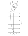
- FIG. 2 shows transmission lines that are not arranged at positions near the first substrate end 1a and positions near the second substrate end 1b, respectively, and are arranged at positions that are not electromagnetically coupled to other transmission lines. It is explanatory drawing which shows the calculation result of S11 of the S parameter in the transmission line. The calculation result shown in FIG. 2 shows that the reflection loss is 40 dB or more, and the transmission line to be calculated in FIG. 2 has a nearly ideal characteristic impedance of 50 ⁇ in the frequency range of 0 to 24 GHz. ing.
- FIG. 3 is an explanatory diagram showing a calculation result of S11 of the S parameter in the transmission line 7-1b when the distance between the first substrate end 1a and the transmission line 7-1b is 20 ⁇ m.
- the calculation result of S11 of the S parameter in the transmission line 7-4b when the distance between the second substrate end 1b and the transmission line 7-4b is 20 ⁇ m is the same as FIG.
- the calculation result shown in FIG. 3 shows that the reflection loss is less than 30 dB, and the transmission lines 7-1b and 7-4b to be calculated in FIG. 3 do not have a characteristic impedance of 50 ⁇ .
- FIG. 4 shows the transmission line 7-2b or the transmission line 7 when the distance between the transmission line 7-2b and the transmission line 7-3b that are electromagnetically coupled to each other is 40 ⁇ m in addition to the electromagnetic field calculation conditions of FIG. It is explanatory drawing which shows the calculation result of S11 of S parameter in -3b. The calculation result shown in FIG. 4 also shows that the reflection loss is less than 30 dB, and the transmission lines 7-2b and 7-3b to be calculated in FIG. 4 do not have a characteristic impedance of 50 ⁇ .
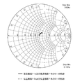
- FIG. 5 is an explanatory diagram in which S11 shown in FIG. 3 and S11 shown in FIG. 4 are plotted on a Smith chart normalized by 50 ⁇ .
- the characteristic impedances of the transmission line 7-1b and the transmission line 7-4b and the characteristic impedances of the transmission line 7-2b and the transmission line 7-3b are not 50 ⁇ .
- FIG. 5 shows that the trajectories of S11 in the transmission lines 7-1b and 7-4b are the same as the trajectories of S11 in the transmission lines 7-2b and 7-3b. ing. Therefore, it can be seen that the characteristic impedances of the transmission line 7-1b and the transmission line 7-4b and the characteristic impedances of the transmission line 7-2b and the transmission line 7-3b are the same.
- the transmission line 7-1b and the transmission line 7-4b are connected to the ground applied to the back surface of the substrate 1.
- the electric flux remains in the substrate 1.
- the first substrate end 1a and the second substrate end 1b act as if they were magnetic walls.
- the electric flux from the transmission line 7-1b and the transmission line 7-4b is prevented from spreading. Further, the spread of the electric flux from the transmission line 7-2b and the transmission line 7-3b to the ground is also suppressed.
- the transmission line 7-2b and the transmission line 7-3b are electromagnetically coupled to each other, the electric flux from the transmission line 7-2b and the electric flux from the transmission line 7-3b are excited in phase and have the same potential. Become. Since the two electric fluxes have the same potential, the spread of the electric fluxes from the transmission line 7-2b and the transmission line 7-3b is also suppressed. The suppression of the spread of the electric flux from the transmission line 7-2b and the transmission line 7-3b is equivalent to the insertion of a magnetic wall in the middle between the transmission line 7-2b and the transmission line 7-3b. It is a state.
- the distance between the magnetic wall equivalently inserted in the intermediate portion and the transmission line 7-2b is equal to the distance between the first substrate end 1a and the transmission line 7-1b.
- the distance between the magnetic wall equivalently inserted in the intermediate portion and the transmission line 7-2b is 20 ⁇ m. is there.
- the distance between the magnetic wall equivalently inserted in the intermediate portion and the transmission line 7-3b is equal to the distance between the second substrate end 1b and the transmission line 7-4b.
- the distance between the magnetic wall equivalently inserted in the intermediate portion and the transmission line 7-3b is 20 ⁇ m. is there.
- FIG. 6 is an explanatory diagram showing the calculation result of S11 when the characteristic impedance is ideal 50 ⁇ and the calculation result of S11 when the transmission line 7-2b and the transmission line 7-3b are not electromagnetically coupled to each other. It is.
- the distance between the electric wall and the transmission line 7-1b and the transmission line 7-4b is 325 ⁇ m.
- the position of the electric wall is the position of the first substrate end 1a and the position of the second substrate end 1b.
- the distance between the electrical wall and the transmission line 7-1b and the transmission line 7-4b is 25 um, 50 um,. 325 um.
- the distance between the electric wall and the transmission line 7-1b and the transmission line 7-4b is changed in 25 um steps.
- the electric wall, the transmission line 7-1b, and the transmission line 7- for obtaining a calculation result equivalent to the calculation result of S11 when the characteristic impedance is ideal 50 ⁇ when they are not electromagnetically coupled to each other.
- the distance from 4b is 325 um.
- the interval of 325 um is the distance between the first substrate end 1a and the transmission line 7-1b and the transmission with the second substrate end 1b when the transmission line 7-2b and the transmission line 7-3b are electromagnetically coupled to each other. It is very large compared to 20 um which is the distance from the line 7-4b. Therefore, when the transmission line 7-2b and the transmission line 7-3b are electromagnetically coupled to each other, the upper margin in FIG. 1 and the lower margin in FIG. Can be miniaturized.
- the upper margin is a region between the first substrate end 1a and the transmission line 7-1b
- the lower margin is a region between the second substrate end 1b and the transmission line 7-4b.
- the first main lines 5-1 to 5-4 and the transmission lines 6-1a, 6-1b, 6-2a, 6-2b, 7-1a to 7-4a, 7-1b to 7-4b The width is assumed to be 90 um.
- the first main lines 5-1 to 5-4 have a line length of 200 ⁇ m
- the transmission lines 6-1a, 6-1b, 6-2a, and 6-2b have a line length of 500 ⁇ m.
- the transmission lines 7-1a to 7-4a have a line length of 100 ⁇ m
- the transmission lines 7-1b to 7-4b have a line length of 500 ⁇ m.
- the connection point between the transmission line 6-1a and the transmission line 6-1b is terminated at 50 ⁇
- the connection point between the transmission line 6-2a and the transmission line 6-2b is terminated at 50 ⁇ .
- FIG. 7 shows the calculation results of the impedances of the output terminals 4-1b to 4-4b of the amplifying elements 4-1 to 4-4 when the characteristic impedance of the transmission lines 7-1b to 7-4b is an ideal 50 ⁇ . It is explanatory drawing shown. When the characteristic impedance of the transmission lines 7-1b to 7-4b is an ideal 50 ⁇ , as shown in FIG. 7, the impedances of the output terminals 4-1b to 4-4b of the amplifier elements 4-1 to 4-4 Are consistent with each other, and the operations of the amplifying elements 4-1 to 4-4 do not vary.
- FIG. 8 is an explanatory diagram illustrating calculation results of impedances of output terminals of a plurality of amplifying elements in the high efficiency amplifier disclosed in Non-Patent Document 1.
- a high-efficiency amplifier corresponding to the high-efficiency amplifier disclosed in Non-Patent Document 1 is mounted with four amplifying elements 4-1 to 4-4.
- 4 shows the calculation results of the impedance of the output terminals 4-1b to 4-4b.
- the high efficiency amplifier is an amplifier in which the transmission line 7-2b and the transmission line 7-3b are not electromagnetically coupled to each other.
- the characteristic impedances of the transmission line 7-1b and the transmission line 7-4b are different from the characteristic impedances of the transmission line 7-2b and the transmission line 7-3b. Therefore, since the loci of the impedances of the output terminals 4-1b to 4-4b of the amplifying elements 4-1 to 4-4 do not match as shown in FIG. 8, the amplifying elements 4-1 to 4-4 operate. Variation occurs. Variations in the operation of the amplifying elements 4-1 to 4-4 cause a signal combining loss in the combining circuit 8, and thus cause a decrease in output power, a decrease in efficiency, and a loop oscillation.
- FIG. 9 is an explanatory diagram illustrating calculation results of impedances of the output terminals 4-1b to 4-4b of the amplification elements 4-1 to 4-4 in the high efficiency amplifier according to the first embodiment.
- the characteristic impedances of the transmission line 7-1b and the transmission line 7-4b and the characteristic impedances of the transmission line 7-2b and the transmission line 7-3b coincide with each other. Accordingly, the loci of the impedances of the output terminals 4-1b to 4-4b of the amplifying elements 4-1 to 4-4 coincide as shown in FIG. 9, so that the amplifying elements 4-1 to 4-4 operate. There is no variation.
- the high-efficiency amplifier according to the first embodiment has higher output and higher efficiency than the high-efficiency amplifier disclosed in Non-Patent Document 1 because there is no variation in the operation of the amplification elements 4-1 to 4-4. High stability and miniaturization can be realized. Further, since the impedance variation can be suppressed over a wide band, a wide band can be realized.
- the characteristic impedance of the transmission lines 7-1b and 7-4b is higher than the ideal characteristic impedance of 50 ⁇ . Therefore, in the high efficiency amplifier of the first embodiment, in order to realize an ideal characteristic impedance of 50 ⁇ , the line widths of the transmission lines 7-1b and 7-4b are set to 90 um as parameters of the substrate 1. It must be thicker than the track width. In the high efficiency amplifier according to the first embodiment, the transmission line 7-2b and the transmission line 7-3b are electromagnetically coupled to each other even when the transmission lines 7-1b and 7-4b have a large line width. Variations in the operations of 4-1 to 4-4 can be suppressed.
- the transmission lines 7-1b and 7-4b can be widened. It is.
- the direct current value that can be passed increases by increasing the line width of the transmission lines 7-1b and 7-4b. .
- the short stubs 7-1 to 7-4 are arranged in a line between the first substrate end 1a and the second substrate end 1b in the substrate 1, and the short stub 7- Among the short stubs 1 to 7-4, the two short stubs 7-2 and 7-3 arranged at adjacent positions among the short stubs arranged at both ends of the row are arranged at positions where they are electromagnetically coupled to each other. As shown, a high efficiency amplifier was constructed. Therefore, the high-efficiency amplifier can suppress variations in operation of the amplification elements 4-1 to 4-4.
- the distribution circuit 3 in FIG. 1 may be a circuit including an amplifying element.
- the amplifying elements included in the distribution circuit 3 are provided to connect the amplifying elements in multiple stages, and amplify the signals to be amplified before the amplifying elements 4-1 to 4-4 amplify the signals to be amplified.
- 1 may be a circuit including an amplifying element.
- the amplifying elements included in the synthesis circuit 8 are provided to connect the amplifying elements in multiple stages, and further amplify the signals amplified by the amplifying elements 4-1 to 4-4.
- FIG. 10 is a block diagram showing a high efficiency amplifier according to the second embodiment.
- the same reference numerals as those in FIG. 10 the same reference numerals as those in FIG.
- the high efficiency amplifier shown in FIG. 10 includes eight amplifying elements 4-1 to 4-8.
- the amplifying elements 4-1 to 4-8 are transistors provided with input terminals 4-1a to 4-8a and output terminals 4-1b to 4-8b, respectively.
- the amplified signal is output from the output terminal 4-nb to the first main line 5-n.
- the amplifying element 4-1 and the amplifying element 4-2 are a pair of amplifying elements
- the amplifying element 4-3 and the amplifying element 4-4 are a pair of amplifying elements
- the amplifying element 4-5 and the amplifying element 4-6 are a pair of amplifying elements
- the amplifying element 4-7 and the amplifying element 4-8 are a pair of amplifying elements.
- the first main lines 5-1 to 5-8 are respectively connected to the output terminals 4-1b to 4-8b of the amplifying elements 4-1 to 4-8 at one end.
- the second main line 6-3 includes a transmission line 6-3a and a transmission line 6-3b.
- the second main line 6-3 has one end connected to the other end of the first main line 5-5 and the other end connected to the other end of the first main line 5-6.
- the second main line 6-4 includes a transmission line 6-4a and a transmission line 6-4b.
- the second main line 6-4 has one end connected to the other end of the first main line 5-7 and the other end connected to the other end of the first main line 5-8.
- the short stubs 10-1 to 10-4 are arranged in a line between the first substrate end 1a and the second substrate end 1b in the substrate 1.
- the short stub 10-1 includes a transmission line 10-1a, a transmission line 10-1b, and a transmission line 10-1c.
- the short stub 10-1 is disposed in the vicinity of the first substrate end 1a, and one end thereof is connected to a connection point (intermediate point) between the transmission line 6-1a and the transmission line 6-1b.
- the transmission line 10-1c is arranged so as to cross the transmission line 6-1a.
- a dielectric member having a relative dielectric constant greater than 1 is inserted between the transmission line 10-1c and the transmission line 6-1a.
- the short stub 10-2 includes a transmission line 10-2a, a transmission line 10-2b, and a transmission line 10-2c.
- the short stub 10-2 is disposed adjacent to the short stub 10-3, and one end thereof is connected to a connection point (intermediate point) between the transmission line 6-2a and the transmission line 6-2b.
- the transmission line 10-2c is disposed so as to cross the transmission line 6-2b.
- a dielectric member having a relative dielectric constant greater than 1 is inserted between the transmission line 10-2c and the transmission line 6-2b.
- the short stub 10-3 includes a transmission line 10-3a, a transmission line 10-3b, and a transmission line 10-3c.
- the short stub 10-3 is disposed at a position adjacent to the short stub 10-2, and one end thereof is connected to a connection point (intermediate point) between the transmission line 6-3a and the transmission line 6-3b.
- the short stub 10-2 and the short stub 10-3 are disposed at positions where they are electromagnetically coupled to each other.
- the transmission line 10-3c is disposed so as to three-dimensionally intersect the transmission line 6-3a.
- a dielectric member having a relative dielectric constant greater than 1 is inserted between the transmission line 10-3c and the transmission line 6-3a.
- the short stub 10-4 includes a transmission line 10-4a, a transmission line 10-4b, and a transmission line 10-4c.
- the short stub 10-4 is disposed in the vicinity of the second substrate end 1b, and one end thereof is connected to a connection point (intermediate point) between the transmission line 6-4a and the transmission line 6-4b.
- the transmission line 10-4c is disposed so as to three-dimensionally intersect with the transmission line 6-4b.
- a dielectric member having a relative dielectric constant greater than 1 is inserted between the transmission line 10-4c and the transmission line 6-4b.
- the distribution circuit 3 When receiving the signal to be amplified from the input terminal 2, the distribution circuit 3 distributes the signal to be amplified and outputs the signal to be amplified after distribution to the amplification elements 4-1 to 4-8.
- the amplification element 4-n 1, 2,..., 8) receives the signal to be amplified after distribution from the distribution circuit 3, it amplifies the signal to be amplified and amplifies it from the output terminal 4-nb. The subsequent signal is output to the first main line 5-n.
- the amplified signals output from the amplifier elements 4-1 to 4-8 are transmitted through the first main lines 5-1 to 5-8.
- the amplified signal transmitted by the first main line 5-1 reaches the synthesis circuit 8 via the transmission line 6-1a, and the amplified signal transmitted by the first main line 5-2 is transmitted.
- the combined circuit 8 is reached via the line 6-1b.
- the amplified signal transmitted through the first main line 5-3 reaches the synthesis circuit 8 via the transmission line 6-2a, and the amplified signal transmitted through the first main line 5-4 is The synthesis circuit 8 is reached via the transmission line 6-2b.
- the amplified signal transmitted by the first main line 5-5 reaches the synthesis circuit 8 via the transmission line 6-3a, and the amplified signal transmitted by the first main line 5-6 is transmitted.
- the combined circuit 8 is reached via the line 6-3b.
- the amplified signal transmitted through the first main line 5-7 reaches the synthesis circuit 8 via the transmission line 6-4a, and the amplified signal transmitted through the first main line 5-8 is Then, the signal reaches the synthesis circuit 8 via the transmission line 6-4b.
- the combining circuit 8 combines the amplified signals transmitted through the transmission lines 6-1a, 6-1b, 6-2a, 6-2b, 6-3a, 6-3b, 6-4a, 6-4b.
- the synthesized signal is output to the output terminal 9.
- the high efficiency amplifier shown in FIG. 1 has the same number of short stubs 7-1 to 7-4 as the amplification elements 4-1 to 4-4, whereas the high efficiency amplifier shown in FIG. Half of the short stubs 10-1 to 10-4 of the elements 4-1 to 4-8 are mounted.
- each of the second main lines 6-1 to 6-4 not both ends of the second main lines 6-1 to 6-4.
- Short stubs 10-1 to 10-4 are respectively connected to the intermediate points.
- FIG. 11 is a circuit diagram showing an example of a general circuit pattern when the short stub 10-1 is connected to the midpoint of the second main line 6-1.
- the transmission line 6-1a and the transmission line 10-1a are arranged side by side in order to reduce the circuit size.
- the transmission line 6-1a and the transmission line 10-1a may be electromagnetically coupled. In a state where the transmission line 6-1a and the transmission line 10-1a are electromagnetically coupled, there is a difference between the impedance viewed from the amplification element 4-1 and the impedance viewed from the amplification element 4-2. Occurs.
- FIG. 12 is an explanatory diagram showing calculation results of the impedance of the output terminal 4-1b of the amplification element 4-1 and the impedance of the output terminal 4-2b of the amplification element 4-2 in the circuit pattern shown in FIG. Impedance calculation conditions are as follows.
- the line widths of the first main lines 5-1 and 5-2 and the transmission lines 6-1a, 6-1b, 10-1a, and 10-1b are 90 um.
- the transmission lines 6-1a, 6-1b, and 10-1a have a line length of 290 ⁇ m
- the first main lines 5-1 and 5-2 have a line length of 10 ⁇ m
- the transmission line 10-1b has a line length of 1850 ⁇ m. .
- the total value of the electrical length of the transmission line 10-1a and the electrical length of the transmission line 10-1b is assumed to be a length of a quarter wavelength at 12 GHz. From FIG. 12, it can be seen that the calculation result of the impedance at the output terminal 4-1b of the amplification element 4-1 is different from the calculation result of the impedance at the output terminal 4-2b of the amplification element 4-2.
- FIG. 13 is an explanatory diagram showing calculation results of the impedance of the output terminal 4-1b of the amplification element 4-1 and the impedance of the output terminal 4-2b of the amplification element 4-2 in the high efficiency amplifier shown in FIG. Impedance calculation conditions are as follows.
- the first main lines 5-1 and 5-2 and the transmission lines 6-1a, 6-1b, 10-1a, 10-1b, and 10-1c have a line width of 90 ⁇ m and the transmission lines 6-1a and 6-1b.
- the length is 290 ⁇ m and the transmission line 10-1c has a line length of 590 ⁇ m.
- the total length of the transmission line 10-1a and the transmission line 10-1b is 1540 um, the electrical length of the transmission line 10-1a, the electrical length of the transmission line 10-1b, and the electrical length of the transmission line 10-1c. Is the length of a quarter wavelength at 12 GHz.
- FIG. 13 shows that the calculation result of the impedance at the output terminal 4-1b of the amplifying element 4-1 matches the calculation result of the impedance at the output terminal 4-2b of the amplifying element 4-2. Therefore, in the high efficiency amplifier shown in FIG. 10, it is possible to suppress variations in operation of the amplification elements 4-1 to 4-8.
- FIG. 14 is an explanatory diagram showing a structure of a three-dimensional intersection.
- FIG. 14 shows a structure of a three-dimensional intersection between the short stub 10-1 and the second main line 6-1 as an example.
- the three-dimensional intersection 20 is a portion where the transmission line 10-1c and the transmission line 6-1a intersect three-dimensionally.
- a dielectric member having a relative dielectric constant greater than 1 is inserted between the transmission line 10-1c and the transmission line 6-1a.
- a dielectric member having a relative dielectric constant larger than 1 an air layer having an air bridge structure or an insulator layer having a structure in which a dielectric is sandwiched can be considered.
- the frequency can be set to an arbitrary frequency.
- the capacitance value of the capacitor can be changed by appropriately adjusting the area where the transmission line 10-1c and the transmission line 6-1a overlap.
- the high-efficiency amplifier shown in FIG. 10 can have a function of a band element filter having a resonance frequency in the region 21 as a cutoff frequency. Therefore, the high-efficiency amplifier shown in FIG. 10 can function as a filter that cuts off harmonics if the resonance frequency in the region 21 is a frequency that is a second harmonic or a third harmonic of the operating frequency.
- the resonance frequency in the region 21 is the frequency of the third harmonic of the operating frequency
- the electrical length of the short stubs 10-1 to 10-4 is a half wavelength length of the frequency of the second harmonic of the operating frequency.
- the distribution circuit 3 in FIG. 10 may be a circuit including an amplifying element.
- the amplifying elements included in the distribution circuit 3 are provided to connect the amplifying elements in multiple stages, and amplify the signals to be amplified before the amplifying elements 4-1 to 4-8 amplify the signals to be amplified.
- 10 may be a circuit including an amplifying element.
- the amplifying elements included in the synthesis circuit 8 are provided to connect the amplifying elements in multiple stages, and further amplify the signals amplified by the amplifying elements 4-1 to 4-8.
- the present invention is suitable for a high efficiency amplifier that amplifies a signal to be amplified.
Landscapes
- Engineering & Computer Science (AREA)
- Power Engineering (AREA)
- Microwave Amplifiers (AREA)
- Amplifiers (AREA)
Abstract
Description
この発明は、増幅対象の信号を増幅する高効率増幅器に関するものである。 The present invention relates to a high efficiency amplifier for amplifying a signal to be amplified.
以下の非特許文献1には、分配された増幅対象の信号を増幅する複数のトランジスタが並列に配置されている高効率増幅器が開示されている。
非特許文献1に開示されている高効率増幅器では、複数のトランジスタの出力端子のそれぞれに、第1主線路の一端が接続されている。また、複数の第1主線路の他端との間には、第2主線路が接続されている。
また、複数の第1主線路の他端には、ショートスタブがそれぞれ接続されている。
Non-Patent
In the high efficiency amplifier disclosed in
Short stubs are connected to the other ends of the plurality of first main lines, respectively.
非特許文献1に開示されている高効率増幅器では、基板の端部付近に配置されるショートスタブの特性インピーダンスと、基板の端部付近以外に配置されるショートスタブとの特性インピーダンスが一致していない。
したがって、複数のトランジスタの出力端子におけるインピーダンスに相違が生じてしまうため、複数のトランジスタの動作にバラツキが生じ、複数のトランジスタの出力端子から出力された信号を合成したときに損失等が発生してしまうという課題があった。
In the high-efficiency amplifier disclosed in
Therefore, since the impedances at the output terminals of the plurality of transistors are different, the operations of the plurality of transistors vary, and loss or the like occurs when the signals output from the output terminals of the plurality of transistors are combined. There was a problem of ending up.
この発明は上記のような課題を解決するためになされたもので、複数の増幅素子の動作のバラツキを抑えることができる高効率増幅器を得ることを目的とする。 The present invention has been made to solve the above-described problems, and an object of the present invention is to obtain a high-efficiency amplifier that can suppress variations in operation of a plurality of amplifying elements.
この発明に係る高効率増幅器は、分配された増幅対象の信号を増幅する複数の増幅素子と、複数の増幅素子のうち、いずれか1つの増幅素子の出力端子と一端が接続されている複数の第1主線路と、複数の第1主線路の中で、複数の増幅素子のうち、一対の増幅素子の出力端子と一端が接続されている2つの第1主線路の他端との間を接続している複数の第2主線路と、複数の第2主線路のそれぞれと接続されている複数のショートスタブとを備え、複数のショートスタブは、基板における第1の基板端と、第1の基板端と対向している基板端である第2の基板端との間に一列に配置されており、複数のショートスタブの中で、列の両端以外に配置されるショートスタブのうち、隣り合う位置に配置される2つのショートスタブは、互いに電磁結合される位置に配置されているようにしたものである。 A high efficiency amplifier according to the present invention includes a plurality of amplifying elements that amplify a distributed signal to be amplified, and a plurality of amplifying elements each having an output terminal and one end connected to each other. Among the plurality of first main lines, among the plurality of first main lines, between the output terminals of the pair of amplifying elements and the other ends of the two first main lines to which one ends are connected. A plurality of second main lines connected to each other, and a plurality of short stubs connected to each of the plurality of second main lines. Are arranged in a row between the second substrate end, which is the substrate end opposite to the substrate end, and among the plurality of short stubs, the adjacent ones of the short stubs arranged outside the both ends of the row. The two short stubs that are placed in a matching position It is obtained as disposed in a position that is magnetostatic coupling.
この発明によれば、複数のショートスタブは、基板における第1の基板端と、第1の基板端と対向している基板端である第2の基板端との間に一列に配置されており、複数のショートスタブの中で、列の両端以外に配置されるショートスタブのうち、隣り合う位置に配置される2つのショートスタブは、互いに電磁結合される位置に配置されているように、高効率増幅器を構成した。したがって、この発明に係る高効率増幅器は、複数の増幅素子の動作のバラツキを抑えることができる。 According to the present invention, the plurality of short stubs are arranged in a line between the first substrate end of the substrate and the second substrate end that is the substrate end facing the first substrate end. Among the plurality of short stubs, two short stubs arranged at adjacent positions among the short stubs arranged at both ends of the row are arranged so as to be arranged at positions where they are electromagnetically coupled to each other. An efficiency amplifier was constructed. Therefore, the high-efficiency amplifier according to the present invention can suppress variations in operation of the plurality of amplifying elements.
以下、この発明をより詳細に説明するために、この発明を実施するための形態について、添付の図面に従って説明する。 Hereinafter, in order to explain the present invention in more detail, modes for carrying out the present invention will be described with reference to the accompanying drawings.
実施の形態1.
図1は、実施の形態1による高効率増幅器を示す構成図である。
図1において、基板1は、高効率増幅器を実装している基板である。
第1の基板端1aは、基板1における図中上側の基板端である。
第2の基板端1bは、第1の基板端1aと対向している図中下側の基板端である。
入力端子2は、増幅対象の信号が入力される端子である。
分配回路3は、入力端子2から入力された増幅対象の信号を分配し、分配後の増幅対象の信号を増幅素子4-1~4-4に出力する回路である。
FIG. 1 is a configuration diagram showing a high efficiency amplifier according to the first embodiment.
In FIG. 1, a
The
The
The
The
増幅素子4-1~4-4は、それぞれ、入力端子4-1a~4-4a及び出力端子4-1b~4-4bを備えているトランジスタである。
増幅素子4-n(n=1,2,3,4)は、分配回路3により分配された増幅対象の信号が入力端子4-naから入力されると、増幅対象の信号を増幅し、出力端子4-nbから増幅後の信号を第1主線路5-nに出力する。
増幅素子4-1~4-4のうち、増幅素子4-1と増幅素子4-2は一対の増幅素子であり、また、増幅素子4-3と増幅素子4-4は一対の増幅素子である。
図1に示す高効率増幅器は、4つの増幅素子4-1~4-4を備えている。しかし、これは一例に過ぎず、高効率増幅器は、4つ以上の偶数個の増幅素子を備えていればよい。
The amplifying elements 4-1 to 4-4 are transistors having input terminals 4-1a to 4-4a and output terminals 4-1b to 4-4b, respectively.
When the amplification target signal distributed by the
Among the amplifying elements 4-1 to 4-4, the amplifying element 4-1 and the amplifying element 4-2 are a pair of amplifying elements, and the amplifying element 4-3 and the amplifying element 4-4 are a pair of amplifying elements. is there.
The high efficiency amplifier shown in FIG. 1 includes four amplifying elements 4-1 to 4-4. However, this is only an example, and the high-efficiency amplifier only needs to include an even number of four or more amplifying elements.
第1主線路5-1~5-4は、それぞれ、増幅素子4-1~4-4の出力端子4-1b~4-4bと一端が接続されている。
第2主線路6-1は、伝送線路6-1a及び伝送線路6-1bを備えている。
第2主線路6-1は、一端が第1主線路5-1の他端と接続され、他端が第1主線路5-2の他端と接続されている。
第2主線路6-2は、伝送線路6-2a及び伝送線路6-2bを備えている。
第2主線路6-2は、一端が第1主線路5-3の他端と接続され、他端が第1主線路5-4の他端と接続されている。
The first main lines 5-1 to 5-4 are respectively connected to the output terminals 4-1b to 4-4b of the amplifying elements 4-1 to 4-4 at one end.
The second main line 6-1 includes a transmission line 6-1a and a transmission line 6-1b.
The second main line 6-1 has one end connected to the other end of the first main line 5-1, and the other end connected to the other end of the first main line 5-2.
The second main line 6-2 includes a transmission line 6-2a and a transmission line 6-2b.
The second main line 6-2 has one end connected to the other end of the first main line 5-3 and the other end connected to the other end of the first main line 5-4.
ショートスタブ7-1~7-4は、基板1における第1の基板端1aと第2の基板端1bとの間に一列に配置されている。
ショートスタブ7-1は、伝送線路7-1a及び伝送線路7-1bを備えている。
ショートスタブ7-1は、第1の基板端1aの近傍に配置されており、一端が第1主線路5-1の他端及び第2主線路6-1の一端とそれぞれ接続されている。
ショートスタブ7-2は、伝送線路7-2a及び伝送線路7-2bを備えている。
ショートスタブ7-2は、ショートスタブ7-3と隣り合う位置に配置されており、一端が第1主線路5-2の他端及び第2主線路6-1の他端とそれぞれ接続されている。
The short stubs 7-1 to 7-4 are arranged in a line between the
The short stub 7-1 includes a transmission line 7-1a and a transmission line 7-1b.
The short stub 7-1 is disposed in the vicinity of the
The short stub 7-2 includes a transmission line 7-2a and a transmission line 7-2b.
The short stub 7-2 is disposed adjacent to the short stub 7-3, and one end is connected to the other end of the first main line 5-2 and the other end of the second main line 6-1. Yes.
ショートスタブ7-3は、伝送線路7-3a及び伝送線路7-3bを備えている。
ショートスタブ7-3は、ショートスタブ7-2と隣り合う位置に配置されており、一端が第1主線路5-3の他端及び第2主線路6-2の一端とそれぞれ接続されている。
ショートスタブ7-2とショートスタブ7-3は、互いに電磁結合される位置に配置されている。
ショートスタブ7-4は、伝送線路7-4a及び伝送線路7-4bを備えている。
ショートスタブ7-4は、第2の基板端1bの近傍に配置されており、一端が第1主線路5-4の他端及び第2主線路6-2の他端とそれぞれ接続されている。
The short stub 7-3 includes a transmission line 7-3a and a transmission line 7-3b.
The short stub 7-3 is disposed adjacent to the short stub 7-2, and one end is connected to the other end of the first main line 5-3 and one end of the second main line 6-2. .
The short stub 7-2 and the short stub 7-3 are arranged at positions where they are electromagnetically coupled to each other.
The short stub 7-4 includes a transmission line 7-4a and a transmission line 7-4b.
The short stub 7-4 is disposed in the vicinity of the
合成回路8は、一端が伝送線路6-1aと伝送線路6-1bの接続点と接続され、他端が伝送線路6-2aと伝送線路6-2bの接続点と接続されている。
合成回路8は、増幅素子4-1~4-4のそれぞれに増幅された信号を合成し、合成後の信号を出力端子9に出力する回路である。
出力端子9は、合成回路8により合成された信号を出力する端子である。
The combining
The
The output terminal 9 is a terminal that outputs a signal synthesized by the
図1に示す高効率増幅器では、ショートスタブ7-1~7-4における伝送線路7-1b~7-4bのそれぞれがグランドと直接接続されている。しかし、これは一例に過ぎず、伝送線路7-1b~7-4bとグランドとの間に、直流成分をカットするコンデンサが接続されていてもよい。 In the high efficiency amplifier shown in FIG. 1, each of the transmission lines 7-1b to 7-4b in the short stubs 7-1 to 7-4 is directly connected to the ground. However, this is only an example, and a capacitor that cuts a DC component may be connected between the transmission lines 7-1b to 7-4b and the ground.
次に、図1に示す高効率増幅器の動作について説明する。
分配回路3は、入力端子2から増幅対象の信号を受けると、増幅対象の信号を分配し、分配後の増幅対象の信号を増幅素子4-1~4-4に出力する。
増幅素子4-n(n=1,2,3,4)は、分配回路3から分配後の増幅対象の信号を受けると、増幅対象の信号を増幅し、出力端子4-nbから増幅後の信号を第1主線路5-nに出力する。
Next, the operation of the high efficiency amplifier shown in FIG. 1 will be described.
When
When the amplification element 4-n (n = 1, 2, 3, 4) receives the signal to be amplified after distribution from the
増幅素子4-1~4-4から出力されたそれぞれの増幅後の信号は、第1主線路5-1~5-4によって伝送される。
第1主線路5-1により伝送された増幅後の信号は、伝送線路6-1aを介して合成回路8に到達し、第1主線路5-2により伝送された増幅後の信号は、伝送線路6-1bを介して合成回路8に到達する。
また、第1主線路5-3により伝送された増幅後の信号は、伝送線路6-2aを介して合成回路8に到達し、第1主線路5-4により伝送された増幅後の信号は、伝送線路6-2bを介して合成回路8に到達する。
合成回路8は、伝送線路6-1a,6-1b,6-2a,6-2bを伝送されてきた増幅後の信号を合成し、合成後の信号を出力端子9に出力する。
The amplified signals output from the amplification elements 4-1 to 4-4 are transmitted through the first main lines 5-1 to 5-4.
The amplified signal transmitted by the first main line 5-1 reaches the
The amplified signal transmitted through the first main line 5-3 reaches the
The combining
次に、図1に示す高効率増幅器の効果を検証する。
ここでは、ショートスタブ7-1~7-4についての電磁界計算を行う条件として、基板1のパラメータが以下のように設定されているものとする。
基板1の厚さは100um、基板1の比誘電率は10、基板1の誘電損失は0、基板1に実装されている金属は金及び基板1の裏面はグランドであるとする。図1に示す高効率増幅器は、基板1の表面に実装されており、基板1の裏面は、基板1の表面と反対側の面である。
また、伝送線路7-1b~7-4bの線路幅は90um、伝送線路7-1b~7-4bの線路長は500umであるとする。
Next, the effect of the high efficiency amplifier shown in FIG. 1 will be verified.
Here, it is assumed that the parameters of the
Assume that the thickness of the
The transmission lines 7-1b to 7-4b have a line width of 90 μm, and the transmission lines 7-1b to 7-4b have a line length of 500 μm.
図2は、第1の基板端1aの近傍の位置及び第2の基板端1bの近傍の位置のそれぞれに配置されていない伝送線路であって、他の伝送線路と電磁結合されない位置に配置されている伝送線路におけるSパラメータのS11の計算結果を示す説明図である。
図2に示す計算結果は、40dB以上の反射損失であることを示しており、図2の計算対象の伝送線路は、0~24GHzの周波数範囲において、ほぼ理想的な50Ωの特性インピーダンスを有している。
FIG. 2 shows transmission lines that are not arranged at positions near the
The calculation result shown in FIG. 2 shows that the reflection loss is 40 dB or more, and the transmission line to be calculated in FIG. 2 has a nearly ideal characteristic impedance of 50Ω in the frequency range of 0 to 24 GHz. ing.
図3は、第1の基板端1aと伝送線路7-1bの間隔が20umである場合の伝送線路7-1bにおけるSパラメータのS11の計算結果を示す説明図である。
第2の基板端1bと伝送線路7-4bの間隔が20umである場合の伝送線路7-4bにおけるSパラメータのS11の計算結果は、図3と同様である。
図3に示す計算結果は、反射損失が30dB未満になることを示しており、図3の計算対象の伝送線路7-1b,7-4bは、特性インピーダンスが50Ωではない。
FIG. 3 is an explanatory diagram showing a calculation result of S11 of the S parameter in the transmission line 7-1b when the distance between the
The calculation result of S11 of the S parameter in the transmission line 7-4b when the distance between the
The calculation result shown in FIG. 3 shows that the reflection loss is less than 30 dB, and the transmission lines 7-1b and 7-4b to be calculated in FIG. 3 do not have a characteristic impedance of 50Ω.
図4は、図3の電磁界計算の条件に加えて、互いに電磁結合される伝送線路7-2bと伝送線路7-3bとの間隔が40umである場合の伝送線路7-2b又は伝送線路7-3bにおけるSパラメータのS11の計算結果を示す説明図である。
図4に示す計算結果も、反射損失が30dB未満になることを示しており、図4の計算対象の伝送線路7-2b,7-3bは、特性インピーダンスが50Ωではない。
4 shows the transmission line 7-2b or the transmission line 7 when the distance between the transmission line 7-2b and the transmission line 7-3b that are electromagnetically coupled to each other is 40 μm in addition to the electromagnetic field calculation conditions of FIG. It is explanatory drawing which shows the calculation result of S11 of S parameter in -3b.
The calculation result shown in FIG. 4 also shows that the reflection loss is less than 30 dB, and the transmission lines 7-2b and 7-3b to be calculated in FIG. 4 do not have a characteristic impedance of 50Ω.
図5は、図3に示すS11及び図4に示すS11のそれぞれを、50Ωで規格化されているスミスチャートにプロットしている説明図である。
伝送線路7-1b及び伝送線路7-4bにおけるそれぞれの特性インピーダンスと、伝送線路7-2b及び伝送線路7-3bにおけるそれぞれの特性インピーダンスとは、どちらも50Ωではない。
しかし、図5は、伝送線路7-1b及び伝送線路7-4bにおけるそれぞれのS11の軌跡と、伝送線路7-2b及び伝送線路7-3bにおけるそれぞれのS11の軌跡とが同一であることを示している。
したがって、伝送線路7-1b及び伝送線路7-4bにおけるそれぞれの特性インピーダンスと、伝送線路7-2b及び伝送線路7-3bにおけるそれぞれの特性インピーダンスとは、同一であることが分かる。
FIG. 5 is an explanatory diagram in which S11 shown in FIG. 3 and S11 shown in FIG. 4 are plotted on a Smith chart normalized by 50Ω.
The characteristic impedances of the transmission line 7-1b and the transmission line 7-4b and the characteristic impedances of the transmission line 7-2b and the transmission line 7-3b are not 50Ω.
However, FIG. 5 shows that the trajectories of S11 in the transmission lines 7-1b and 7-4b are the same as the trajectories of S11 in the transmission lines 7-2b and 7-3b. ing.
Therefore, it can be seen that the characteristic impedances of the transmission line 7-1b and the transmission line 7-4b and the characteristic impedances of the transmission line 7-2b and the transmission line 7-3b are the same.
ここで、基板1の外側の比誘電率よりも基板1の比誘電率の方が高いため、伝送線路7-1b及び伝送線路7-4bから、基板1の裏面に施されているグランドへの電束は、基板1内に留まる。
伝送線路7-1b及び伝送線路7-4bからの電束が基板1内に留まる状況では、第1の基板端1a及び第2の基板端1bが、あたかも、磁気壁のように作用しており、伝送線路7-1b及び伝送線路7-4bからの電束は、広がりが抑えられている。
また、伝送線路7-2b及び伝送線路7-3bからグランドへの電束についても、広がりが抑えられている。
伝送線路7-2bと伝送線路7-3bは、互いに電磁結合されているため、伝送線路7-2bからの電束と、伝送線路7-3bからの電束とが同相励振して同電位となる。2つの電束が同電位となることで、伝送線路7-2b及び伝送線路7-3bからの電束についても、広がりが抑えられている。
伝送線路7-2b及び伝送線路7-3bからの電束の広がりが抑えられていることは、伝送線路7-2bと伝送線路7-3bとの中間部に磁気壁が挿入されたことと等価な状態である。
Here, since the relative permittivity of the
In the situation where the electric flux from the transmission line 7-1b and the transmission line 7-4b stays in the
Further, the spread of the electric flux from the transmission line 7-2b and the transmission line 7-3b to the ground is also suppressed.
Since the transmission line 7-2b and the transmission line 7-3b are electromagnetically coupled to each other, the electric flux from the transmission line 7-2b and the electric flux from the transmission line 7-3b are excited in phase and have the same potential. Become. Since the two electric fluxes have the same potential, the spread of the electric fluxes from the transmission line 7-2b and the transmission line 7-3b is also suppressed.
The suppression of the spread of the electric flux from the transmission line 7-2b and the transmission line 7-3b is equivalent to the insertion of a magnetic wall in the middle between the transmission line 7-2b and the transmission line 7-3b. It is a state.
等価的に中間部に挿入された磁気壁と伝送線路7-2bとの間隔は、第1の基板端1aと伝送線路7-1bとの間隔と等しい。ここでは、第1の基板端1aと伝送線路7-1bとの間隔が20umであるとしているため、等価的に中間部に挿入された磁気壁と伝送線路7-2bとの間隔は、20umである。
また、等価的に中間部に挿入された磁気壁と伝送線路7-3bとの間隔は、第2の基板端1bと伝送線路7-4bとの間隔と等しい。ここでは、第2の基板端1bと伝送線路7-4bとの間隔が20umであるとしているため、等価的に中間部に挿入された磁気壁と伝送線路7-3bとの間隔は、20umである。
The distance between the magnetic wall equivalently inserted in the intermediate portion and the transmission line 7-2b is equal to the distance between the
In addition, the distance between the magnetic wall equivalently inserted in the intermediate portion and the transmission line 7-3b is equal to the distance between the
図6は、特性インピーダンスが理想的な50ΩとなるときのS11の計算結果と、伝送線路7-2bと伝送線路7-3bが互いに電磁結合されていないときのS11の計算結果とを示す説明図である。
図6において、特性インピーダンスが理想的な50Ωとなるときは、電気壁と伝送線路7-1b及び伝送線路7-4bとの間隔は、325umである。電気壁の位置は、第1の基板端1aの位置及び第2の基板端1bの位置である。
伝送線路7-2bと伝送線路7-3bが互いに電磁結合されていないときは、電気壁と伝送線路7-1b及び伝送線路7-4bとの間隔は、25um、50um、・・・、300um又は325umである。電気壁と伝送線路7-1b及び伝送線路7-4bとの間隔は、25umステップで変えられている。
FIG. 6 is an explanatory diagram showing the calculation result of S11 when the characteristic impedance is ideal 50Ω and the calculation result of S11 when the transmission line 7-2b and the transmission line 7-3b are not electromagnetically coupled to each other. It is.
In FIG. 6, when the characteristic impedance is an ideal 50Ω, the distance between the electric wall and the transmission line 7-1b and the transmission line 7-4b is 325 μm. The position of the electric wall is the position of the
When the transmission line 7-2b and the transmission line 7-3b are not electromagnetically coupled to each other, the distance between the electrical wall and the transmission line 7-1b and the transmission line 7-4b is 25 um, 50 um,. 325 um. The distance between the electric wall and the transmission line 7-1b and the transmission line 7-4b is changed in 25 um steps.
図6より、互いに電磁結合されていないときに、特性インピーダンスが理想的な50ΩとなるときのS11の計算結果と同等の計算結果を得るための電気壁と伝送線路7-1b及び伝送線路7-4bとの間隔は、325umであることが分かる。
325umの間隔は、伝送線路7-2bと伝送線路7-3bが互いに電磁結合されているときの、第1の基板端1aと伝送線路7-1bとの間隔及び第2の基板端1bと伝送線路7-4bとの間隔である20umと比べて、極めて大きい。
したがって、伝送線路7-2bと伝送線路7-3bが互いに電磁結合されているときは、基板1における図1中の上部余白及び図1中の下部余白を小さくすることができるため、高効率増幅器の小型化を図ることができる。上部余白とは、第1の基板端1aと伝送線路7-1bとの間の領域であり、下部余白とは、第2の基板端1bと伝送線路7-4bとの間の領域である。
From FIG. 6, the electric wall, the transmission line 7-1b, and the transmission line 7- for obtaining a calculation result equivalent to the calculation result of S11 when the characteristic impedance is ideal 50Ω when they are not electromagnetically coupled to each other. It can be seen that the distance from 4b is 325 um.
The interval of 325 um is the distance between the
Therefore, when the transmission line 7-2b and the transmission line 7-3b are electromagnetically coupled to each other, the upper margin in FIG. 1 and the lower margin in FIG. Can be miniaturized. The upper margin is a region between the
次に、図1に示す高効率増幅器の効果を増幅素子から見たインピーダンスで検証する。
ここでは、第1主線路5-1~5-4及び伝送線路6-1a、6-1b、6-2a、6-2b、7-1a~7-4a、7-1b~7-4bの線路幅は90umであるとする。
第1主線路5-1~5-4の線路長は200um、伝送線路6-1a、6-1b、6-2a、6-2bの線路長は500umであるとする。
伝送線路7-1a~7-4aの線路長は100um、伝送線路7-1b~7-4bの線路長は500umであるとする。
伝送線路6-1aと伝送線路6-1bの接続点は、50Ωで終端され、伝送線路6-2aと伝送線路6-2bの接続点は、50Ωで終端されているものとする。
Next, the effect of the high-efficiency amplifier shown in FIG.
Here, the first main lines 5-1 to 5-4 and the transmission lines 6-1a, 6-1b, 6-2a, 6-2b, 7-1a to 7-4a, 7-1b to 7-4b The width is assumed to be 90 um.
Assume that the first main lines 5-1 to 5-4 have a line length of 200 μm, and the transmission lines 6-1a, 6-1b, 6-2a, and 6-2b have a line length of 500 μm.
It is assumed that the transmission lines 7-1a to 7-4a have a line length of 100 μm, and the transmission lines 7-1b to 7-4b have a line length of 500 μm.
The connection point between the transmission line 6-1a and the transmission line 6-1b is terminated at 50Ω, and the connection point between the transmission line 6-2a and the transmission line 6-2b is terminated at 50Ω.
図7は、伝送線路7-1b~7-4bにおける特性インピーダンスが理想的な50Ωとなるときの増幅素子4-1~4-4の出力端子4-1b~4-4bのインピーダンスの計算結果を示す説明図である。
伝送線路7-1b~7-4bにおける特性インピーダンスが理想的な50Ωとなるときは、図7に示すように、増幅素子4-1~4-4の出力端子4-1b~4-4bのインピーダンスの軌跡が一致しており、増幅素子4-1~4-4の動作にバラツキが生じない。
FIG. 7 shows the calculation results of the impedances of the output terminals 4-1b to 4-4b of the amplifying elements 4-1 to 4-4 when the characteristic impedance of the transmission lines 7-1b to 7-4b is an ideal 50Ω. It is explanatory drawing shown.
When the characteristic impedance of the transmission lines 7-1b to 7-4b is an ideal 50Ω, as shown in FIG. 7, the impedances of the output terminals 4-1b to 4-4b of the amplifier elements 4-1 to 4-4 Are consistent with each other, and the operations of the amplifying elements 4-1 to 4-4 do not vary.
図8は、非特許文献1に開示されている高効率増幅器における複数の増幅素子の出力端子のインピーダンスの計算結果を示す説明図である。
図8では、非特許文献1に開示されている高効率増幅器に相当する高効率増幅器が、4つの増幅素子4-1~4-4を実装しているものとして、増幅素子4-1~4-4の出力端子4-1b~4-4bのインピーダンスの計算結果を示している。
当該高効率増幅器は、伝送線路7-2bと伝送線路7-3bが互いに電磁結合されていない増幅器である。
したがって、当該高効率増幅器では、伝送線路7-1b及び伝送線路7-4bにおけるそれぞれの特性インピーダンスと、伝送線路7-2b及び伝送線路7-3bにおけるそれぞれの特性インピーダンスとが異なる。よって、増幅素子4-1~4-4の出力端子4-1b~4-4bのインピーダンスの軌跡は、図8に示すように、一致しないため、増幅素子4-1~4-4は、動作にバラツキが生じる。
増幅素子4-1~4-4の動作のバラツキは、合成回路8での信号の合成損失の要因になるため、出力電力の低下、効率の低下及びループ発振の要因になる。
FIG. 8 is an explanatory diagram illustrating calculation results of impedances of output terminals of a plurality of amplifying elements in the high efficiency amplifier disclosed in
In FIG. 8, it is assumed that a high-efficiency amplifier corresponding to the high-efficiency amplifier disclosed in
The high efficiency amplifier is an amplifier in which the transmission line 7-2b and the transmission line 7-3b are not electromagnetically coupled to each other.
Therefore, in the high efficiency amplifier, the characteristic impedances of the transmission line 7-1b and the transmission line 7-4b are different from the characteristic impedances of the transmission line 7-2b and the transmission line 7-3b. Therefore, since the loci of the impedances of the output terminals 4-1b to 4-4b of the amplifying elements 4-1 to 4-4 do not match as shown in FIG. 8, the amplifying elements 4-1 to 4-4 operate. Variation occurs.
Variations in the operation of the amplifying elements 4-1 to 4-4 cause a signal combining loss in the combining
図9は、実施の形態1の高効率増幅器における増幅素子4-1~4-4の出力端子4-1b~4-4bのインピーダンスの計算結果を示す説明図である。
実施の形態1の高効率増幅器では、伝送線路7-1b及び伝送線路7-4bにおけるそれぞれの特性インピーダンスと、伝送線路7-2b及び伝送線路7-3bにおけるそれぞれの特性インピーダンスとが一致する。したがって、増幅素子4-1~4-4の出力端子4-1b~4-4bのインピーダンスの軌跡は、図9に示すように、一致するため、増幅素子4-1~4-4は、動作にバラツキが生じない。
実施の形態1の高効率増幅器は、増幅素子4-1~4-4の動作にバラツキが生じないため、非特許文献1に開示されている高効率増幅器よりも、高出力化、高効率化、高安定化及び小型化を実現することができる。また、広帯域に亘ってインピーダンスのバラツキを抑圧できるため、広帯域化を実現することができる。
FIG. 9 is an explanatory diagram illustrating calculation results of impedances of the output terminals 4-1b to 4-4b of the amplification elements 4-1 to 4-4 in the high efficiency amplifier according to the first embodiment.
In the high efficiency amplifier according to the first embodiment, the characteristic impedances of the transmission line 7-1b and the transmission line 7-4b and the characteristic impedances of the transmission line 7-2b and the transmission line 7-3b coincide with each other. Accordingly, the loci of the impedances of the output terminals 4-1b to 4-4b of the amplifying elements 4-1 to 4-4 coincide as shown in FIG. 9, so that the amplifying elements 4-1 to 4-4 operate. There is no variation.
The high-efficiency amplifier according to the first embodiment has higher output and higher efficiency than the high-efficiency amplifier disclosed in
実施の形態1の高効率増幅器では、伝送線路7-1b,7-4bの特性インピーダンスが、理想的な50Ωの特性インピーダンスよりも高くなる。したがって、実施の形態1の高効率増幅器では、理想的な50Ωの特性インピーダンスを実現するには、伝送線路7-1b,7-4bの線路幅を、基板1のパラメータとして設定している90umの線路幅よりも太くする必要がある。
実施の形態1の高効率増幅器では、伝送線路7-1b,7-4bの線路幅を太くしても、伝送線路7-2bと伝送線路7-3bを互いに電磁結合されることで、増幅素子4-1~4-4の動作のバラツキを抑えることができる。
したがって、実施の形態1の高効率増幅器では、例えば、ショートスタブ7-1,7-4を電源の供給路として用いる場合、伝送線路7-1b,7-4bの線路幅を太くすることが可能である。
例えば、ショートスタブ7-1,7-4を電源の供給路として用いる場合、伝送線路7-1b,7-4bの線路幅を太くすることで、流すことが可能な直流の電流値が増加する。
In the high efficiency amplifier of the first embodiment, the characteristic impedance of the transmission lines 7-1b and 7-4b is higher than the ideal characteristic impedance of 50Ω. Therefore, in the high efficiency amplifier of the first embodiment, in order to realize an ideal characteristic impedance of 50Ω, the line widths of the transmission lines 7-1b and 7-4b are set to 90 um as parameters of the
In the high efficiency amplifier according to the first embodiment, the transmission line 7-2b and the transmission line 7-3b are electromagnetically coupled to each other even when the transmission lines 7-1b and 7-4b have a large line width. Variations in the operations of 4-1 to 4-4 can be suppressed.
Therefore, in the high efficiency amplifier of the first embodiment, for example, when the short stubs 7-1 and 7-4 are used as power supply paths, the transmission lines 7-1b and 7-4b can be widened. It is.
For example, when the short stubs 7-1 and 7-4 are used as power supply paths, the direct current value that can be passed increases by increasing the line width of the transmission lines 7-1b and 7-4b. .
以上の実施の形態1は、ショートスタブ7-1~7-4が、基板1における第1の基板端1aと第2の基板端1bとの間に一列に配置されており、ショートスタブ7-1~7-4の中で、列の両端以外に配置されるショートスタブのうち、隣り合う位置に配置される2つのショートスタブ7-2,7-3は、互いに電磁結合される位置に配置されているように、高効率増幅器を構成した。したがって、高効率増幅器は、増幅素子4-1~4-4の動作のバラツキを抑えることができる。
図1の分配回路3は、増幅素子を含む回路でもよい。分配回路3に含まれる増幅素子は、増幅素子を多段接続するために設けられ、増幅素子4-1~4-4が増幅対象の信号を増幅する前に、増幅対象の信号を増幅する。
また、図1の合成回路8は、増幅素子を含む回路でもよい。合成回路8に含まれる増幅素子は、増幅素子を多段接続するために設けられ、増幅素子4-1~4-4による増幅後の信号を更に増幅する。
In the first embodiment described above, the short stubs 7-1 to 7-4 are arranged in a line between the
The
1 may be a circuit including an amplifying element. The amplifying elements included in the
実施の形態2.
実施の形態2では、ショートスタブ7-1~7-4が、それぞれ第2主線路6-1~6-4と立体交差するように配置されている高効率増幅器について説明する。
図10は、実施の形態2による高効率増幅器を示す構成図である。図10において、図1と同一符号は同一又は相当部分を示すので説明を省略する。
In the second embodiment, a high-efficiency amplifier in which short stubs 7-1 to 7-4 are arranged so as to three-dimensionally intersect with second main lines 6-1 to 6-4 will be described.
FIG. 10 is a block diagram showing a high efficiency amplifier according to the second embodiment. In FIG. 10, the same reference numerals as those in FIG.
図10に示す高効率増幅器は、8つの増幅素子4-1~4-8を備えている。
増幅素子4-1~4-8は、それぞれ、入力端子4-1a~4-8a及び出力端子4-1b~4-8bを備えているトランジスタである。
増幅素子4-n(n=1,2,・・・,8)は、分配回路3により分配された増幅対象の信号が入力端子4-naから入力されると、増幅対象の信号を増幅し、出力端子4-nbから増幅後の信号を第1主線路5-nに出力する。
増幅素子4-1~4-8のうち、増幅素子4-1と増幅素子4-2は一対の増幅素子であり、増幅素子4-3と増幅素子4-4は一対の増幅素子である。
また、増幅素子4-5と増幅素子4-6は一対の増幅素子であり、増幅素子4-7と増幅素子4-8は一対の増幅素子である。
The high efficiency amplifier shown in FIG. 10 includes eight amplifying elements 4-1 to 4-8.
The amplifying elements 4-1 to 4-8 are transistors provided with input terminals 4-1a to 4-8a and output terminals 4-1b to 4-8b, respectively.
When the amplification target signal distributed by the
Among the amplifying elements 4-1 to 4-8, the amplifying element 4-1 and the amplifying element 4-2 are a pair of amplifying elements, and the amplifying element 4-3 and the amplifying element 4-4 are a pair of amplifying elements.
The amplifying element 4-5 and the amplifying element 4-6 are a pair of amplifying elements, and the amplifying element 4-7 and the amplifying element 4-8 are a pair of amplifying elements.
第1主線路5-1~5-8は、それぞれ、増幅素子4-1~4-8の出力端子4-1b~4-8bと一端が接続されている。
第2主線路6-3は、伝送線路6-3a及び伝送線路6-3bを備えている。
第2主線路6-3は、一端が第1主線路5-5の他端と接続され、他端が第1主線路5-6の他端と接続されている。
第2主線路6-4は、伝送線路6-4a及び伝送線路6-4bを備えている。
第2主線路6-4は、一端が第1主線路5-7の他端と接続され、他端が第1主線路5-8の他端と接続されている。
The first main lines 5-1 to 5-8 are respectively connected to the output terminals 4-1b to 4-8b of the amplifying elements 4-1 to 4-8 at one end.
The second main line 6-3 includes a transmission line 6-3a and a transmission line 6-3b.
The second main line 6-3 has one end connected to the other end of the first main line 5-5 and the other end connected to the other end of the first main line 5-6.
The second main line 6-4 includes a transmission line 6-4a and a transmission line 6-4b.
The second main line 6-4 has one end connected to the other end of the first main line 5-7 and the other end connected to the other end of the first main line 5-8.
ショートスタブ10-1~10-4は、基板1における第1の基板端1aと第2の基板端1bとの間に一列に配置されている。
ショートスタブ10-1は、伝送線路10-1a、伝送線路10-1b及び伝送線路10-1cを備えている。
ショートスタブ10-1は、第1の基板端1aの近傍に配置されており、一端が伝送線路6-1aと伝送線路6-1bの接続点(中間点)と接続されている。
伝送線路10-1cは、伝送線路6-1aと立体交差するように配置されている。
伝送線路10-1cと伝送線路6-1aとの間には、比誘電率が1よりも大きい誘電部材が挿入されている。
The short stubs 10-1 to 10-4 are arranged in a line between the
The short stub 10-1 includes a transmission line 10-1a, a transmission line 10-1b, and a transmission line 10-1c.
The short stub 10-1 is disposed in the vicinity of the
The transmission line 10-1c is arranged so as to cross the transmission line 6-1a.
A dielectric member having a relative dielectric constant greater than 1 is inserted between the transmission line 10-1c and the transmission line 6-1a.
ショートスタブ10-2は、伝送線路10-2a、伝送線路10-2b及び伝送線路10-2cを備えている。
ショートスタブ10-2は、ショートスタブ10-3と隣り合う位置に配置されており、一端が伝送線路6-2aと伝送線路6-2bの接続点(中間点)と接続されている。
伝送線路10-2cは、伝送線路6-2bと立体交差するように配置されている。
伝送線路10-2cと伝送線路6-2bとの間には、比誘電率が1よりも大きい誘電部材が挿入されている。
The short stub 10-2 includes a transmission line 10-2a, a transmission line 10-2b, and a transmission line 10-2c.
The short stub 10-2 is disposed adjacent to the short stub 10-3, and one end thereof is connected to a connection point (intermediate point) between the transmission line 6-2a and the transmission line 6-2b.
The transmission line 10-2c is disposed so as to cross the transmission line 6-2b.
A dielectric member having a relative dielectric constant greater than 1 is inserted between the transmission line 10-2c and the transmission line 6-2b.
ショートスタブ10-3は、伝送線路10-3a、伝送線路10-3b及び伝送線路10-3cを備えている。
ショートスタブ10-3は、ショートスタブ10-2と隣り合う位置に配置されており、一端が伝送線路6-3aと伝送線路6-3bの接続点(中間点)と接続されている。
ショートスタブ10-2とショートスタブ10-3は、互いに電磁結合される位置に配置されている。
伝送線路10-3cは、伝送線路6-3aと立体交差するように配置されている。
伝送線路10-3cと伝送線路6-3aとの間には、比誘電率が1よりも大きい誘電部材が挿入されている。
The short stub 10-3 includes a transmission line 10-3a, a transmission line 10-3b, and a transmission line 10-3c.
The short stub 10-3 is disposed at a position adjacent to the short stub 10-2, and one end thereof is connected to a connection point (intermediate point) between the transmission line 6-3a and the transmission line 6-3b.
The short stub 10-2 and the short stub 10-3 are disposed at positions where they are electromagnetically coupled to each other.
The transmission line 10-3c is disposed so as to three-dimensionally intersect the transmission line 6-3a.
A dielectric member having a relative dielectric constant greater than 1 is inserted between the transmission line 10-3c and the transmission line 6-3a.
ショートスタブ10-4は、伝送線路10-4a、伝送線路10-4b及び伝送線路10-4cを備えている。
ショートスタブ10-4は、第2の基板端1bの近傍に配置されており、一端が伝送線路6-4aと伝送線路6-4bの接続点(中間点)と接続されている。
伝送線路10-4cは、伝送線路6-4bと立体交差するように配置されている。
伝送線路10-4cと伝送線路6-4bとの間には、比誘電率が1よりも大きい誘電部材が挿入されている。
The short stub 10-4 includes a transmission line 10-4a, a transmission line 10-4b, and a transmission line 10-4c.
The short stub 10-4 is disposed in the vicinity of the
The transmission line 10-4c is disposed so as to three-dimensionally intersect with the transmission line 6-4b.
A dielectric member having a relative dielectric constant greater than 1 is inserted between the transmission line 10-4c and the transmission line 6-4b.
次に、図10に示す高効率増幅器の動作について説明する。
分配回路3は、入力端子2から増幅対象の信号を受けると、増幅対象の信号を分配し、分配後の増幅対象の信号を増幅素子4-1~4-8に出力する。
増幅素子4-n(n=1,2,・・・,8)は、分配回路3から分配後の増幅対象の信号を受けると、増幅対象の信号を増幅し、出力端子4-nbから増幅後の信号を第1主線路5-nに出力する。
Next, the operation of the high efficiency amplifier shown in FIG. 10 will be described.
When receiving the signal to be amplified from the
When the amplification element 4-n (n = 1, 2,..., 8) receives the signal to be amplified after distribution from the
増幅素子4-1~4-8から出力されたそれぞれの増幅後の信号は、第1主線路5-1~5-8によって伝送される。
第1主線路5-1により伝送された増幅後の信号は、伝送線路6-1aを介して合成回路8に到達し、第1主線路5-2により伝送された増幅後の信号は、伝送線路6-1bを介して合成回路8に到達する。
また、第1主線路5-3により伝送された増幅後の信号は、伝送線路6-2aを介して合成回路8に到達し、第1主線路5-4により伝送された増幅後の信号は、伝送線路6-2bを介して合成回路8に到達する。
第1主線路5-5により伝送された増幅後の信号は、伝送線路6-3aを介して合成回路8に到達し、第1主線路5-6により伝送された増幅後の信号は、伝送線路6-3bを介して合成回路8に到達する。
また、第1主線路5-7により伝送された増幅後の信号は、伝送線路6-4aを介して合成回路8に到達し、第1主線路5-8により伝送された増幅後の信号は、伝送線路6-4bを介して合成回路8に到達する。
合成回路8は、伝送線路6-1a,6-1b,6-2a,6-2b,6-3a,6-3b,6-4a,6-4bを伝送されてきた増幅後の信号を合成し、合成後の信号を出力端子9に出力する。
The amplified signals output from the amplifier elements 4-1 to 4-8 are transmitted through the first main lines 5-1 to 5-8.
The amplified signal transmitted by the first main line 5-1 reaches the
The amplified signal transmitted through the first main line 5-3 reaches the
The amplified signal transmitted by the first main line 5-5 reaches the
The amplified signal transmitted through the first main line 5-7 reaches the
The combining
図1に示す高効率増幅器は、増幅素子4-1~4-4と同数のショートスタブ7-1~7-4を実装しているのに対して、図10に示す高効率増幅器は、増幅素子4-1~4-8の半数のショートスタブ10-1~10-4を実装している。
図10に示す高効率増幅器では、ショートスタブの実装数を削減するために、第2主線路6-1~6-4の両端ではなく、第2主線路6-1~6-4におけるそれぞれの中間点に、ショートスタブ10-1~10-4をそれぞれ接続している。
The high efficiency amplifier shown in FIG. 1 has the same number of short stubs 7-1 to 7-4 as the amplification elements 4-1 to 4-4, whereas the high efficiency amplifier shown in FIG. Half of the short stubs 10-1 to 10-4 of the elements 4-1 to 4-8 are mounted.
In the high-efficiency amplifier shown in FIG. 10, in order to reduce the number of short stubs mounted, each of the second main lines 6-1 to 6-4, not both ends of the second main lines 6-1 to 6-4. Short stubs 10-1 to 10-4 are respectively connected to the intermediate points.
ここで、ショートスタブ10-1~10-4のうち、ショートスタブ10-1を例にとって、第2主線路6-1の中間点にショートスタブ10-1を接続する場合の回路パターンについて説明する。
図11は、第2主線路6-1の中間点にショートスタブ10-1を接続する場合の一般的な回路パターンの一例を示す回路図である。
図11に示す回路パターンでは、回路サイズを低減するために、伝送線路6-1aと伝送線路10-1aとが並べて配置されている。
しかし、伝送線路6-1aと伝送線路10-1aとが並べて配置される場合、伝送線路6-1aと伝送線路10-1aとが電磁結合してしまうことがある。
伝送線路6-1aと伝送線路10-1aとが電磁結合している状態では、増幅素子4-1から出力側を見たインピーダンスと、増幅素子4-2から出力側を見たインピーダンスとに相違が生じる。
Here, of the short stubs 10-1 to 10-4, the short stub 10-1 is taken as an example and a circuit pattern when the short stub 10-1 is connected to the midpoint of the second main line 6-1 will be described. .
FIG. 11 is a circuit diagram showing an example of a general circuit pattern when the short stub 10-1 is connected to the midpoint of the second main line 6-1.
In the circuit pattern shown in FIG. 11, the transmission line 6-1a and the transmission line 10-1a are arranged side by side in order to reduce the circuit size.
However, when the transmission line 6-1a and the transmission line 10-1a are arranged side by side, the transmission line 6-1a and the transmission line 10-1a may be electromagnetically coupled.
In a state where the transmission line 6-1a and the transmission line 10-1a are electromagnetically coupled, there is a difference between the impedance viewed from the amplification element 4-1 and the impedance viewed from the amplification element 4-2. Occurs.
図12は、図11に示す回路パターンにおける増幅素子4-1の出力端子4-1bのインピーダンスと増幅素子4-2の出力端子4-2bのインピーダンスとの計算結果を示す説明図である。
インピーダンスの計算条件は、以下の通りである。
第1主線路5-1,5-2及び伝送線路6-1a,6-1b,10-1a,10-1bの線路幅は90umであるとする。
伝送線路6-1a,6-1b,10-1aの線路長は290um、第1主線路5-1,5-2の線路長は10um、伝送線路10-1bの線路長は1850umであるとする。
また、伝送線路10-1aの電気長と伝送線路10-1bの電気長との合計値は、12GHzで4分の1波長の長さであるとする。
図12より、増幅素子4-1の出力端子4-1bにおけるインピーダンスの計算結果と増幅素子4-2の出力端子4-2bにおけるインピーダンスの計算結果とが異なることが分かる。
FIG. 12 is an explanatory diagram showing calculation results of the impedance of the output terminal 4-1b of the amplification element 4-1 and the impedance of the output terminal 4-2b of the amplification element 4-2 in the circuit pattern shown in FIG.
Impedance calculation conditions are as follows.
The line widths of the first main lines 5-1 and 5-2 and the transmission lines 6-1a, 6-1b, 10-1a, and 10-1b are 90 um.
The transmission lines 6-1a, 6-1b, and 10-1a have a line length of 290 μm, the first main lines 5-1 and 5-2 have a line length of 10 μm, and the transmission line 10-1b has a line length of 1850 μm. .
Further, the total value of the electrical length of the transmission line 10-1a and the electrical length of the transmission line 10-1b is assumed to be a length of a quarter wavelength at 12 GHz.
From FIG. 12, it can be seen that the calculation result of the impedance at the output terminal 4-1b of the amplification element 4-1 is different from the calculation result of the impedance at the output terminal 4-2b of the amplification element 4-2.
図10に示す高効率増幅器では、図11に示すような回路パターンではなく、伝送線路10-1cが伝送線路6-1aと立体交差するように配置され、伝送線路6-1aと伝送線路10-1aとが並べて配置されない回路パターンになっている。
図13は、図10に示す高効率増幅器における増幅素子4-1の出力端子4-1bのインピーダンスと増幅素子4-2の出力端子4-2bのインピーダンスとの計算結果を示す説明図である。
インピーダンスの計算条件は、以下の通りである。
第1主線路5-1,5-2及び伝送線路6-1a,6-1b,10-1a,10-1b,10-1cの線路幅は90um、伝送線路6-1a,6-1bの線路長は290um、伝送線路10-1cの線路長は590umであるとする。
また、伝送線路10-1aと伝送線路10-1bとの線路長の合計値は1540um、伝送線路10-1aの電気長と伝送線路10-1bの電気長と伝送線路10-1cの電気長との合計値は、12GHzで4分の1波長の長さであるとする。
図13より、増幅素子4-1の出力端子4-1bにおけるインピーダンスの計算結果と増幅素子4-2の出力端子4-2bにおけるインピーダンスの計算結果とが一致していることが分かる。
したがって、図10に示す高効率増幅器では、増幅素子4-1~4-8の動作のバラツキを抑えることができる。
In the high efficiency amplifier shown in FIG. 10, the transmission line 10-1c is not three-dimensionally crossed with the transmission line 6-1a, instead of the circuit pattern shown in FIG. 11, and the transmission line 6-1a and the transmission line 10- The
FIG. 13 is an explanatory diagram showing calculation results of the impedance of the output terminal 4-1b of the amplification element 4-1 and the impedance of the output terminal 4-2b of the amplification element 4-2 in the high efficiency amplifier shown in FIG.
Impedance calculation conditions are as follows.
The first main lines 5-1 and 5-2 and the transmission lines 6-1a, 6-1b, 10-1a, 10-1b, and 10-1c have a line width of 90 μm and the transmission lines 6-1a and 6-1b. It is assumed that the length is 290 μm and the transmission line 10-1c has a line length of 590 μm.
The total length of the transmission line 10-1a and the transmission line 10-1b is 1540 um, the electrical length of the transmission line 10-1a, the electrical length of the transmission line 10-1b, and the electrical length of the transmission line 10-1c. Is the length of a quarter wavelength at 12 GHz.
FIG. 13 shows that the calculation result of the impedance at the output terminal 4-1b of the amplifying element 4-1 matches the calculation result of the impedance at the output terminal 4-2b of the amplifying element 4-2.
Therefore, in the high efficiency amplifier shown in FIG. 10, it is possible to suppress variations in operation of the amplification elements 4-1 to 4-8.
次に、ショートスタブ10-1~10-4と第2主線路6-1~4-4との立体交差の構造について説明する。
図14は、立体交差の構造を示す説明図である。
図14は、一例として、ショートスタブ10-1と第2主線路6-1との立体交差の構造を示している。
図14において、立体交差部20は、伝送線路10-1cと伝送線路6-1aとが立体交差している部分である。
伝送線路10-1cと伝送線路6-1aとの間には、比誘電率が1よりも大きい誘電部材が挿入されている。
比誘電率が1よりも大きい誘電部材として、エアブリッジ構造の空気層又は誘電体が挟み込まれた構造の絶縁体層などが考えられる。
Next, the structure of the three-dimensional intersection between the short stubs 10-1 to 10-4 and the second main lines 6-1 to 4-4 will be described.
FIG. 14 is an explanatory diagram showing a structure of a three-dimensional intersection.
FIG. 14 shows a structure of a three-dimensional intersection between the short stub 10-1 and the second main line 6-1 as an example.
In FIG. 14, the three-
A dielectric member having a relative dielectric constant greater than 1 is inserted between the transmission line 10-1c and the transmission line 6-1a.
As a dielectric member having a relative dielectric constant larger than 1, an air layer having an air bridge structure or an insulator layer having a structure in which a dielectric is sandwiched can be considered.
ここで、立体交差部20において、伝送線路10-1c及び伝送線路6-1aによって形成されるコンデンサの容量値を適宜設定することで、図14に示す破線で囲まれている領域21での共振周波数を任意の周波数に設定することができる。
コンデンサの容量値は、伝送線路10-1cと伝送線路6-1aが重なる面積を適宜調整することで変えることができる。
図10に示す高効率増幅器は、領域21での共振周波数を遮断周波数とする帯域素子フィルタの機能を有することができる。
したがって、図10に示す高効率増幅器は、領域21での共振周波数が、動作周波数の2倍波の周波数又は3倍波の周波数であれば、高調波を遮断するフィルタとして機能することができる。
領域21での共振周波数が、動作周波数の3倍波の周波数であり、ショートスタブ10-1~10-4の電気長が、動作周波数の2倍波の周波数で2分の1波長の長さである場合を想定する。この場合、図10に示す高効率増幅器では、増幅素子4-1~4-8に対してF級の高調波整合条件を与えることができるため、増幅素子4-1~4-8の効率を高めることができる。
図10の分配回路3は、増幅素子を含む回路でもよい。分配回路3に含まれる増幅素子は、増幅素子を多段接続するために設けられ、増幅素子4-1~4-8が増幅対象の信号を増幅する前に、増幅対象の信号を増幅する。
また、図10の合成回路8は、増幅素子を含む回路でもよい。合成回路8に含まれる増幅素子は、増幅素子を多段接続するために設けられ、増幅素子4-1~4-8による増幅後の信号を更に増幅する。
Here, in the three-
The capacitance value of the capacitor can be changed by appropriately adjusting the area where the transmission line 10-1c and the transmission line 6-1a overlap.
The high-efficiency amplifier shown in FIG. 10 can have a function of a band element filter having a resonance frequency in the
Therefore, the high-efficiency amplifier shown in FIG. 10 can function as a filter that cuts off harmonics if the resonance frequency in the
The resonance frequency in the
The
10 may be a circuit including an amplifying element. The amplifying elements included in the
なお、本願発明はその発明の範囲内において、各実施の形態の自由な組み合わせ、あるいは各実施の形態の任意の構成要素の変形、もしくは各実施の形態において任意の構成要素の省略が可能である。 In the present invention, within the scope of the invention, any combination of the embodiments, any modification of any component in each embodiment, or omission of any component in each embodiment is possible. .
この発明は、増幅対象の信号を増幅する高効率増幅器に適している。 The present invention is suitable for a high efficiency amplifier that amplifies a signal to be amplified.
1 基板、1a 第1の基板端、1b 第2の基板端、2 入力端子、3 分配回路、4-1~4-8 増幅素子、4-1a~4-8a 入力端子、4-1b~4-8b 出力端子、5-1~5-8 第1主線路、6-1~6-4 第2主線路、6-1a~6-4a,6-1b~6-4b 伝送線路、7-1~7-4 ショートスタブ、7-1a~7-4a,7-1b~7-4b 伝送線路、8 合成回路、9 出力端子、10-1~10-4 ショートスタブ、10-1a~10-4a,10-1b~10-4b,10-1c~10-4c 伝送線路、20 立体交差部、21 領域。 1 board, 1a first board edge, 1b second board edge, 2 input terminal, 3 distribution circuit, 4-1 to 4-8 amplifying element, 4-1a to 4-8a input terminal, 4-1b to 4 -8b Output terminal, 5-1 to 5-8, first main line, 6-1 to 6-4, second main line, 6-1a to 6-4a, 6-1b to 6-4b transmission line, 7-1 ~ 7-4 Short stub, 7-1a to 7-4a, 7-1b to 7-4b Transmission line, 8 Composite circuit, 9 Output terminal, 10-1 to 10-4 Short stub, 10-1a to 10-4a , 10-1b to 10-4b, 10-1c to 10-4c, transmission line, 20 intersection, 21 area.
Claims (4)
前記複数の増幅素子のうち、いずれか1つの増幅素子の出力端子と一端が接続されている複数の第1主線路と、
前記複数の第1主線路の中で、前記複数の増幅素子のうち、一対の増幅素子の出力端子と一端が接続されている2つの第1主線路の他端との間を接続している複数の第2主線路と、
前記複数の第2主線路のそれぞれと接続されている複数のショートスタブとを備え、
前記複数のショートスタブは、基板における第1の基板端と、前記第1の基板端と対向している基板端である第2の基板端との間に一列に配置されており、
前記複数のショートスタブの中で、列の両端以外に配置されるショートスタブのうち、隣り合う位置に配置される2つのショートスタブは、互いに電磁結合される位置に配置されていることを特徴とする高効率増幅器。 A plurality of amplifying elements for amplifying the distributed signals to be amplified;
Among the plurality of amplifying elements, a plurality of first main lines to which one output terminal and one end of the amplifying element are connected,
Among the plurality of first main lines, the output terminals of the pair of amplifying elements among the plurality of amplifying elements are connected to the other ends of the two first main lines to which one ends are connected. A plurality of second main lines;
A plurality of short stubs connected to each of the plurality of second main lines,
The plurality of short stubs are arranged in a line between a first substrate end of the substrate and a second substrate end that is a substrate end facing the first substrate end,
Of the plurality of short stubs, two short stubs arranged at adjacent positions among the short stubs arranged at both ends of the row are arranged at positions where they are electromagnetically coupled to each other. High efficiency amplifier.
Priority Applications (4)
| Application Number | Priority Date | Filing Date | Title |
|---|---|---|---|
| EP18921684.9A EP3790192B1 (en) | 2018-06-07 | 2018-06-07 | High-efficiency amplifier |
| JP2020523933A JP6827593B2 (en) | 2018-06-07 | 2018-06-07 | High efficiency amplifier |
| PCT/JP2018/021899 WO2019234885A1 (en) | 2018-06-07 | 2018-06-07 | High-efficiency amplifier |
| US17/094,451 US11621674B2 (en) | 2018-06-07 | 2020-11-10 | High-efficiency amplifier |
Applications Claiming Priority (1)
| Application Number | Priority Date | Filing Date | Title |
|---|---|---|---|
| PCT/JP2018/021899 WO2019234885A1 (en) | 2018-06-07 | 2018-06-07 | High-efficiency amplifier |
Related Child Applications (1)
| Application Number | Title | Priority Date | Filing Date |
|---|---|---|---|
| US17/094,451 Continuation US11621674B2 (en) | 2018-06-07 | 2020-11-10 | High-efficiency amplifier |
Publications (1)
| Publication Number | Publication Date |
|---|---|
| WO2019234885A1 true WO2019234885A1 (en) | 2019-12-12 |
Family
ID=68769767
Family Applications (1)
| Application Number | Title | Priority Date | Filing Date |
|---|---|---|---|
| PCT/JP2018/021899 Ceased WO2019234885A1 (en) | 2018-06-07 | 2018-06-07 | High-efficiency amplifier |
Country Status (4)
| Country | Link |
|---|---|
| US (1) | US11621674B2 (en) |
| EP (1) | EP3790192B1 (en) |
| JP (1) | JP6827593B2 (en) |
| WO (1) | WO2019234885A1 (en) |
Families Citing this family (1)
| Publication number | Priority date | Publication date | Assignee | Title |
|---|---|---|---|---|
| KR20250015480A (en) * | 2023-07-25 | 2025-02-03 | 고려대학교 산학협력단 | A wideband matching apparatus and method for frequency multiplier |
Citations (5)
| Publication number | Priority date | Publication date | Assignee | Title |
|---|---|---|---|---|
| JPH05129854A (en) * | 1991-11-01 | 1993-05-25 | Mitsubishi Electric Corp | Broadband field effect transistor amplifier |
| JPH07283668A (en) * | 1994-04-04 | 1995-10-27 | Mitsubishi Electric Corp | High frequency amplifier |
| JP2000286338A (en) * | 1999-03-30 | 2000-10-13 | Denso Corp | High frequency circuit structure and method of manufacturing the same |
| JP2008113402A (en) * | 2006-05-09 | 2008-05-15 | Mitsubishi Electric Corp | amplifier |
| JP2015517771A (en) * | 2012-05-23 | 2015-06-22 | 中国▲電▼子科技集▲団▼公司第五十五研究所China Electronics Technology Group Corporation No.55 Research Institute | Amplifying circuit for cross wiring of DC signal and microwave signal |
Family Cites Families (6)
| Publication number | Priority date | Publication date | Assignee | Title |
|---|---|---|---|---|
| JPH10163772A (en) * | 1996-10-04 | 1998-06-19 | Sanyo Electric Co Ltd | Power amplifier and chip carrier |
| JP3464383B2 (en) | 1998-05-20 | 2003-11-10 | 三菱電機株式会社 | Power distribution circuit and power amplifier |
| JP2002135014A (en) | 2000-10-19 | 2002-05-10 | Mitsubishi Electric Corp | Branch circuits, high-pass filters and duplexers |
| JP4712546B2 (en) * | 2005-12-05 | 2011-06-29 | 三菱電機株式会社 | Microwave amplifier |
| US9397616B2 (en) * | 2013-11-06 | 2016-07-19 | Commscope Technologies Llc | Quasi-doherty architecture amplifier and method |
| JP2015171107A (en) | 2014-03-10 | 2015-09-28 | 富士通株式会社 | Distribution type amplifier |
-
2018
- 2018-06-07 WO PCT/JP2018/021899 patent/WO2019234885A1/en not_active Ceased
- 2018-06-07 JP JP2020523933A patent/JP6827593B2/en active Active
- 2018-06-07 EP EP18921684.9A patent/EP3790192B1/en active Active
-
2020
- 2020-11-10 US US17/094,451 patent/US11621674B2/en active Active
Patent Citations (5)
| Publication number | Priority date | Publication date | Assignee | Title |
|---|---|---|---|---|
| JPH05129854A (en) * | 1991-11-01 | 1993-05-25 | Mitsubishi Electric Corp | Broadband field effect transistor amplifier |
| JPH07283668A (en) * | 1994-04-04 | 1995-10-27 | Mitsubishi Electric Corp | High frequency amplifier |
| JP2000286338A (en) * | 1999-03-30 | 2000-10-13 | Denso Corp | High frequency circuit structure and method of manufacturing the same |
| JP2008113402A (en) * | 2006-05-09 | 2008-05-15 | Mitsubishi Electric Corp | amplifier |
| JP2015517771A (en) * | 2012-05-23 | 2015-06-22 | 中国▲電▼子科技集▲団▼公司第五十五研究所China Electronics Technology Group Corporation No.55 Research Institute | Amplifying circuit for cross wiring of DC signal and microwave signal |
Non-Patent Citations (1)
| Title |
|---|
| See also references of EP3790192A4 * |
Also Published As
| Publication number | Publication date |
|---|---|
| JP6827593B2 (en) | 2021-02-10 |
| EP3790192B1 (en) | 2022-12-07 |
| JPWO2019234885A1 (en) | 2020-12-17 |
| US20210075375A1 (en) | 2021-03-11 |
| EP3790192A1 (en) | 2021-03-10 |
| EP3790192A4 (en) | 2021-05-12 |
| US11621674B2 (en) | 2023-04-04 |
Similar Documents
| Publication | Publication Date | Title |
|---|---|---|
| JP6513225B2 (en) | Doherty amplifier | |
| JP5424790B2 (en) | High power amplifier | |
| CN111342817A (en) | Impedance control unit, balun unit, electronic device, and doherty amplifier | |
| WO2011102187A1 (en) | Directional coupler | |
| JP2013102363A (en) | Power amplification circuit and high frequency module | |
| WO2019234885A1 (en) | High-efficiency amplifier | |
| US7288995B2 (en) | Power amplifier of a transmitter | |
| TWI730354B (en) | Power distribution/combination device | |
| JP4652095B2 (en) | Power amplifier | |
| US20200358408A1 (en) | Amplifier module | |
| JP6366887B2 (en) | High frequency power amplifier | |
| WO2021140975A1 (en) | High frequency amplifier | |
| JP5902070B2 (en) | Power amplifier and transmitter | |
| JPWO2005093948A1 (en) | amplifier | |
| CN112154603B (en) | Amplifier | |
| KR101367310B1 (en) | Wideband planar 3 db branch line coupler improving selectivity | |
| WO2021141030A1 (en) | High frequency amplifier | |
| JP4082920B2 (en) | Delay filter and distortion compensation amplifier using the same | |
| JP2008035335A (en) | High frequency circuit board and manufacturing method thereof | |
| TWI894674B (en) | Coupler structure and related radio frequency circuit | |
| US20190296701A1 (en) | High frequency circuit and high frequency power amplifier | |
| JP7532987B2 (en) | Amplification equipment | |
| JP4202833B2 (en) | amplifier | |
| JP4153898B2 (en) | RF power amplifier module | |
| JPH0583051A (en) | Balanced type amplifier |
Legal Events
| Date | Code | Title | Description |
|---|---|---|---|
| 121 | Ep: the epo has been informed by wipo that ep was designated in this application |
Ref document number: 18921684 Country of ref document: EP Kind code of ref document: A1 |
|
| ENP | Entry into the national phase |
Ref document number: 2020523933 Country of ref document: JP Kind code of ref document: A |
|
| ENP | Entry into the national phase |
Ref document number: 2018921684 Country of ref document: EP Effective date: 20201202 |
|
| NENP | Non-entry into the national phase |
Ref country code: DE |