WO2019082480A1 - Optical semiconductor device package, optical semiconductor device, and manufacturing method for optical semiconductor device package - Google Patents
Optical semiconductor device package, optical semiconductor device, and manufacturing method for optical semiconductor device packageInfo
- Publication number
- WO2019082480A1 WO2019082480A1 PCT/JP2018/030603 JP2018030603W WO2019082480A1 WO 2019082480 A1 WO2019082480 A1 WO 2019082480A1 JP 2018030603 W JP2018030603 W JP 2018030603W WO 2019082480 A1 WO2019082480 A1 WO 2019082480A1
- Authority
- WO
- WIPO (PCT)
- Prior art keywords
- metal
- optical semiconductor
- semiconductor device
- package
- electrode potential
- Prior art date
- Legal status (The legal status is an assumption and is not a legal conclusion. Google has not performed a legal analysis and makes no representation as to the accuracy of the status listed.)
- Ceased
Links
Images


Classifications
-
- H—ELECTRICITY
- H10—SEMICONDUCTOR DEVICES; ELECTRIC SOLID-STATE DEVICES NOT OTHERWISE PROVIDED FOR
- H10H—INORGANIC LIGHT-EMITTING SEMICONDUCTOR DEVICES HAVING POTENTIAL BARRIERS
- H10H20/00—Individual inorganic light-emitting semiconductor devices having potential barriers, e.g. light-emitting diodes [LED]
- H10H20/80—Constructional details
- H10H20/85—Packages
- H10H20/855—Optical field-shaping means, e.g. lenses
- H10H20/856—Reflecting means
-
- H—ELECTRICITY
- H10—SEMICONDUCTOR DEVICES; ELECTRIC SOLID-STATE DEVICES NOT OTHERWISE PROVIDED FOR
- H10H—INORGANIC LIGHT-EMITTING SEMICONDUCTOR DEVICES HAVING POTENTIAL BARRIERS
- H10H20/00—Individual inorganic light-emitting semiconductor devices having potential barriers, e.g. light-emitting diodes [LED]
- H10H20/01—Manufacture or treatment
-
- H—ELECTRICITY
- H10—SEMICONDUCTOR DEVICES; ELECTRIC SOLID-STATE DEVICES NOT OTHERWISE PROVIDED FOR
- H10H—INORGANIC LIGHT-EMITTING SEMICONDUCTOR DEVICES HAVING POTENTIAL BARRIERS
- H10H20/00—Individual inorganic light-emitting semiconductor devices having potential barriers, e.g. light-emitting diodes [LED]
- H10H20/80—Constructional details
- H10H20/85—Packages
- H10H20/857—Interconnections, e.g. lead-frames, bond wires or solder balls
-
- H—ELECTRICITY
- H10—SEMICONDUCTOR DEVICES; ELECTRIC SOLID-STATE DEVICES NOT OTHERWISE PROVIDED FOR
- H10H—INORGANIC LIGHT-EMITTING SEMICONDUCTOR DEVICES HAVING POTENTIAL BARRIERS
- H10H20/00—Individual inorganic light-emitting semiconductor devices having potential barriers, e.g. light-emitting diodes [LED]
- H10H20/01—Manufacture or treatment
- H10H20/036—Manufacture or treatment of packages
- H10H20/0363—Manufacture or treatment of packages of optical field-shaping means
-
- H—ELECTRICITY
- H10—SEMICONDUCTOR DEVICES; ELECTRIC SOLID-STATE DEVICES NOT OTHERWISE PROVIDED FOR
- H10H—INORGANIC LIGHT-EMITTING SEMICONDUCTOR DEVICES HAVING POTENTIAL BARRIERS
- H10H20/00—Individual inorganic light-emitting semiconductor devices having potential barriers, e.g. light-emitting diodes [LED]
- H10H20/01—Manufacture or treatment
- H10H20/036—Manufacture or treatment of packages
- H10H20/0364—Manufacture or treatment of packages of interconnections
-
- H—ELECTRICITY
- H10—SEMICONDUCTOR DEVICES; ELECTRIC SOLID-STATE DEVICES NOT OTHERWISE PROVIDED FOR
- H10H—INORGANIC LIGHT-EMITTING SEMICONDUCTOR DEVICES HAVING POTENTIAL BARRIERS
- H10H20/00—Individual inorganic light-emitting semiconductor devices having potential barriers, e.g. light-emitting diodes [LED]
- H10H20/80—Constructional details
- H10H20/85—Packages
- H10H20/8506—Containers
Definitions
- the upper part of copper or copper alloy is plated with nickel as a barrier layer for preventing copper diffusion, and palladium plating for preventing diffusion of sulfur based brightener in nickel plating is provided thereon.
- a method of applying and performing silver plating on the top for example, refer to Patent Document 2.
- the optical semiconductor device when the optical semiconductor device is driven for a long period of time, light emitted from the optical semiconductor element is irradiated to titanium oxide which is a white pigment contained in the envelope resin functioning as a reflector (that is, a reflector). Accordingly, the life of the optical semiconductor device is further shortened because active oxygen (specifically, superoxide anion) generated by exciting titanium oxide to exhibit photocatalytic action turns black of silver oxide to silver oxide. New problems occur.
- the optical semiconductor device which concerns on one form of this invention is provided with the optical semiconductor element and the said package for optical semiconductor devices which mounts the said optical semiconductor element.
- optical semiconductor device package 10 the optical semiconductor device 20, and the method for manufacturing the optical semiconductor device package 10 according to the present invention have been described above based on the embodiment, the present invention is limited to this embodiment. It is not a thing. Without departing from the spirit of the present invention, various modifications that can be conceived by those skilled in the art may be applied to the present embodiment, or another embodiment constructed by combining some of the components in the embodiments may be included within the scope of the present invention. Contained within.
Landscapes
- Led Device Packages (AREA)
Abstract
Description
本発明は光半導体装置用パッケージ、光半導体装置および光半導体装置用パッケージの製造方法に関し、特に長期間使用した場合における光半導体装置の劣化を防止する技術に関する。 The present invention relates to an optical semiconductor device package, an optical semiconductor device, and a method of manufacturing the optical semiconductor device package, and more particularly to a technique for preventing deterioration of the optical semiconductor device when used for a long time.
従来の光半導体装置用パッケージでは、外囲樹脂に包囲された領域(以下、「光半導体素子搭載領域」ともいう)の最表層(つまり、光半導体素子が搭載される底面)に、反射被膜として銀被膜が形成されている。この領域は光半導体装置用パッケージの外側に効率よく光を反射させて発光効率を向上させる役目をなす。なお、本明細書では、発光素子および受光素子等の光半導体を光半導体素子といい、光半導体素子を搭載するためのパッケージ自体を光半導体装置用パッケージといい、光半導体素子が搭載された光半導体装置用パッケージ全体(光半導体素子と光半導体装置用パッケージとを合わせたもの)を光半導体装置という。 In a conventional package for an optical semiconductor device, a reflective coating is provided on the outermost layer (that is, the bottom surface on which the optical semiconductor element is mounted) of the region (hereinafter, also referred to as "optical semiconductor element mounting region") A silver film is formed. This region serves to efficiently reflect light to the outside of the optical semiconductor device package to improve the light emission efficiency. In this specification, an optical semiconductor such as a light emitting element and a light receiving element is referred to as an optical semiconductor element, a package for mounting the optical semiconductor element is referred to as an optical semiconductor device package, and an optical semiconductor element is mounted. The entire package for a semiconductor device (a combination of an optical semiconductor element and a package for an optical semiconductor device) is called an optical semiconductor device.
光半導体装置用パッケージの銀被膜の層構成としては、銅または銅合金上に銀めっきが形成されることが多い(例えば、特許文献1参照)。しかしながら、このような層構成の銀めっきは光半導体装置の長期間使用による発熱の影響で下地金属の銅が銀めっき表面に拡散することにより、銀めっき表面が銅色に変色して反射率の低下を招く問題がある。 As a layer structure of the silver film of the package for optical semiconductor devices, silver plating is formed in many cases on copper or copper alloy (for example, refer patent document 1). However, the silver plating of such a layer configuration is discolored due to the copper of the base metal diffusing to the silver plating surface under the influence of heat generation due to the long-term use of the optical semiconductor device, and the silver plating surface is discolored to copper color, and the reflectance is There is a problem that causes deterioration.
一方、その不都合を防止する方法として、銅または銅合金上部に、銅拡散防止のバリア層としてニッケルめっきを施し、その上部にニッケルめっき中の硫黄系光沢剤の拡散を防止するためのパラジウムめっきを施し、その上部に銀めっきを施す方法がある(例えば、特許文献2参照)。 On the other hand, as a method of preventing the inconvenience, the upper part of copper or copper alloy is plated with nickel as a barrier layer for preventing copper diffusion, and palladium plating for preventing diffusion of sulfur based brightener in nickel plating is provided thereon. There is a method of applying and performing silver plating on the top (for example, refer to Patent Document 2).
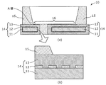
図5は、銅拡散防止のバリア層としてニッケルおよびパラジウムを用いた従来の光半導体装置用パッケージ50を示す断面図である。より詳しくは、図5の(a)は、従来の光半導体装置用パッケージ50本体の断面図である。図5の(b)は、図5の(a)のA部の拡大図である。
FIG. 5 is a cross-sectional view showing a
図5の(a)および(b)において、光半導体装置用パッケージ50では、リードフレームを構成する回路基板54は、例えば銅または銅合金51からなる金属基材の略全面に、ニッケルめっき52aおよびパラジウムめっき52bからなる下地めっき、並びに、銀または銀合金53からなる反射層がこの順に積層されている。光半導体装置用パッケージ50の内部空間には所定の光半導体素子をダイボンディングおよびワイヤーボンディングを行った後、封止樹脂が充填される。
In (a) and (b) of FIG. 5, in the
上記のような層構成の場合、光半導体装置の長期熱履歴による下地銅の銀被膜表面への拡散による反射率低下は防止できる。 In the case of the layer configuration as described above, it is possible to prevent the decrease in reflectance due to the diffusion of the base copper to the surface of the silver film due to the long-term thermal history of the optical semiconductor device.
しかしながら、光半導体装置の長期間駆動の際に、光半導体素子から発光される光が、リフレクター(つまり、反射体)として機能する外囲樹脂中に含まれる白色顔料である酸化チタンに照射されることにより、酸化チタンが励起して光触媒作用を示すことによって生じる活性酸素(具体的には、スーパーオキサイドアニオン)が銀を酸化銀にして黒色化するために、光半導体装置の寿命がよりいっそう短くなるという新たな問題が発生する。 However, when the optical semiconductor device is driven for a long period of time, light emitted from the optical semiconductor element is irradiated to titanium oxide which is a white pigment contained in the envelope resin functioning as a reflector (that is, a reflector). Accordingly, the life of the optical semiconductor device is further shortened because active oxygen (specifically, superoxide anion) generated by exciting titanium oxide to exhibit photocatalytic action turns black of silver oxide to silver oxide. New problems occur.
本発明は以上の各課題に鑑みてなされたものであって、光半導体装置の発熱による下地銅の拡散に起因する銀めっき変色に起因する反射被膜の反射率の低下と、長期間駆動により誘発される外囲樹脂中の酸化チタンによる光触媒作用で生成する活性酸素による銀黒色化に起因する光半導体装置の短寿命化とを効果的に抑制することができる光半導体装置用パッケージ等の提供を目的とする。 The present invention has been made in view of the above problems, and the reflectance of the reflective coating is lowered due to the silver plating discoloration caused by the diffusion of the base copper due to the heat generation of the optical semiconductor device, and the induction is caused by the long-term drive. Provided is a package for an optical semiconductor device which can effectively suppress the shortening of the life of the optical semiconductor device caused by the blackening of silver by the active oxygen generated by the photocatalytic action of titanium oxide in the surrounding resin. To aim.
上記従来の課題を解決するために、本発明の一形態に係る光半導体装置用パッケージは、光半導体素子を搭載するための光半導体装置用パッケージであって、回路基板と、前記回路基板上に形成され、前記光半導体素子が搭載される前記回路基板上の領域の外周を囲む、白色顔料を含む壁部とを備え、前記回路基板は、第1の標準電極電位を有する第1の金属と、前記第1の金属の上面の一部に形成され、前記第1の標準電極電位よりも大きい第2の標準電極電位を有する第2の金属と、前記第1の金属の上面および前記第2の金属の上面に積層され、前記第1の標準電極電位よりも大きく、かつ、前記第2の標準電極電位よりも小さい第3の標準電極電位を有する第3の金属とで構成される。 In order to solve the above-mentioned conventional problems, a package for an optical semiconductor device according to an aspect of the present invention is a package for an optical semiconductor device for mounting an optical semiconductor element, and a circuit substrate and a circuit substrate on the circuit substrate. And a wall portion including a white pigment surrounding the outer periphery of the region on the circuit board on which the optical semiconductor element is mounted, the circuit board comprising a first metal having a first standard electrode potential A second metal formed on a part of the upper surface of the first metal and having a second standard electrode potential larger than the first standard electrode potential; an upper surface of the first metal and the second metal And a third metal having a third standard electrode potential which is larger than the first standard electrode potential and smaller than the second standard electrode potential.
また、上記従来の課題を解決するために、本発明の一形態に係る光半導体装置は、光半導体素子と、前記光半導体素子を搭載する上記光半導体装置用パッケージとを備える。 Moreover, in order to solve the said conventional subject, the optical semiconductor device which concerns on one form of this invention is provided with the optical semiconductor element and the said package for optical semiconductor devices which mounts the said optical semiconductor element.
さらに、上記従来の課題を解決するために、本発明の一形態に係る光半導体装置用パッケージの製造方法は、光半導体素子を搭載するための光半導体装置用パッケージの製造方法であって、第1の標準電極電位を有する第1の金属を準備する工程と、前記第1の金属の上面の一部に、前記第1の標準電極電位よりも大きい第2の標準電極電位を有する第2の金属を形成する工程と、前記第1の金属の上面および前記第2の金属の上面に、前記第1の標準電極電位よりも大きく、かつ、前記第2の標準電極電位よりも小さい第3の標準電極電位を有する第3の金属を形成する工程とを含む。 Furthermore, in order to solve the above-mentioned conventional problems, a method of manufacturing a package for an optical semiconductor device according to an aspect of the present invention is a method of manufacturing a package for an optical semiconductor device for mounting an optical semiconductor device, Providing a first metal having a standard electrode potential of 1; and a second standard electrode potential having a second standard electrode potential greater than the first standard electrode potential on a portion of the top surface of the first metal. A step of forming a metal, and a third upper surface of the first metal and an upper surface of the second metal, which is larger than the first standard electrode potential and smaller than the second standard electrode potential Forming a third metal having a standard electrode potential.
本発明に係る光半導体装置用パッケージ等により、光半導体装置の発熱による下地銅の拡散に起因する銀めっき変色に起因する反射被膜の反射率の低下と、長期間駆動により誘発される外囲樹脂中の酸化チタンによる光触媒作用で生成する活性酸素による銀黒色化に起因する光半導体装置の短寿命化とが効果的に抑制される。 The package for an optical semiconductor device according to the present invention, the decrease in the reflectance of the reflective film due to the silver plating discoloration caused by the diffusion of the base copper due to the heat generation of the optical semiconductor device, and the envelope resin induced by long-time driving The shortening of the life of the optical semiconductor device due to the silver blackening due to the active oxygen generated by the photocatalytic action of titanium oxide in the medium is effectively suppressed.
従って光半導体装置を長期間駆動させても反射率の高い本来の銀の特性が損なわれず、光半導体装置として十分な発光輝度が得られるという効果が奏される。 Therefore, even if the optical semiconductor device is driven for a long period of time, the original characteristic of silver having high reflectance is not impaired, and an effect that sufficient light emission luminance as the optical semiconductor device can be obtained is exerted.
以下、本発明の各実施の形態を添付の図面を参照しながら説明する。なお、当然ながら本発明はこれらの実施形式に限定されるものではなく、本発明の技術的範囲を逸脱しない範囲で適宜変更して実施することができる。つまり、以下で説明する実施の形態は、いずれも本発明の一具体例を示すものである。以下の実施の形態で示される数値、形状、材料、構成要素、構成要素の配置位置および接続形態、工程、工程の順序等は、一例であり、本発明を限定する主旨ではない。また、以下の実施の形態における構成要素のうち、本発明の最上位概念を示す独立請求項に記載されていない構成要素については、任意の構成要素として説明される。また、各図は、必ずしも厳密に図示したものではない。各図において、実質的に同一の構成については同一の符号を付し、重複する説明は省略または簡略化する。 Hereinafter, embodiments of the present invention will be described with reference to the attached drawings. Naturally, the present invention is not limited to these embodiments, and can be appropriately modified and implemented without departing from the technical scope of the present invention. That is, all the embodiments described below show one specific example of the present invention. The numerical values, shapes, materials, components, arrangement positions and connection forms of the components, steps, order of steps, and the like shown in the following embodiments are merely examples, and are not intended to limit the present invention. In addition, among the components in the following embodiments, components not described in the independent claim showing the highest concept of the present invention are described as optional components. Moreover, each figure is not necessarily illustrated exactly. In the drawings, substantially the same components are denoted by the same reference numerals, and redundant description will be omitted or simplified.
(光半導体装置用パッケージの構成)
図1は、本発明の実施の形態に係る光半導体装置用パッケージ10の断面図である。より詳しくは、図1の(a)は、本実施の形態に係る光半導体装置用パッケージ10本体の断面図である。図1の(b)は、図1の(a)のA部の拡大図である。なお、本実施の形態に係る光半導体装置用パッケージ10は、光半導体素子を搭載するのに適したパッケージであるが、搭載される素子としては、光半導体素子に限定されず、通常の半導体素子であってもよい。つまり、本実施の形態に係る光半導体装置用パッケージ10は、「半導体装置用パッケージ」と呼ぶこともできるパッケージである。また、光半導体装置用パッケージ10は、全体として、直方体状の構造を有する。
(Configuration of package for optical semiconductor device)
FIG. 1 is a cross-sectional view of an optical
図1の(a)において、本実施の形態に係る光半導体装置用パッケージ10は、銅、鉄、ニッケル、または、それらの少なくとも二つを含む合金からなる金属基材をプレスまたはエッチングなどの成型技術により所望の形状に加工し、所定の表面処理および白色顔料を含む外囲樹脂の樹脂成形を施すことで構成されている。より詳しくは、本実施の形態に係る光半導体装置用パッケージ10は、光半導体素子を搭載するための光半導体装置用パッケージであって、リードフレームを構成する回路基板14と、回路基板14上に形成され、光半導体素子が搭載される回路基板14上の領域(光半導体素子搭載領域16)の外周を囲む、白色顔料を含む壁部である外囲樹脂15とを備える。回路基板14は、第1の標準電極電位を有する第1の金属11と、第1の金属11の上面の一部に形成され、第1の標準電極電位よりも大きい第2の標準電極電位を有する第2の金属12と、第1の金属11の上面および第2の金属12の上面に積層され、第1の標準電極電位よりも大きく、かつ、第2の標準電極電位よりも小さい第3の標準電極電位を有する第3の金属13とで構成される。
In FIG. 1A, the
なお、図1では、第2の金属12が、第1の金属11の上面だけでなく、上面、下面および側面を含む全表面の一部に形成され、第3の金属13が、第1の金属11および第2の金属12の全ての露出面を覆うように形成された構造例が示されている。また、回路基板14は、相互に離隔(図1では、左右に離隔)した一対の回路基板で構成されている。一対の回路基板14は、同一平面上に配置され、同一の構造を有する。
In FIG. 1, the
本実施の形態の構成では、半導体素子または光半導体素子(図示せず)を搭載する光半導体素子搭載領域16には、回路基板14の最表面に、光の反射率を向上させるための第3の金属13の一例である銀または銀を含む合金めっき層が形成されている。
In the configuration of the present embodiment, a third of the optical semiconductor
具体的には図1の(b)に示すように、光半導体素子搭載領域16では、リードフレームを構成する回路基板14は、金属基材としての第1の金属11の一例である銅または銅合金基材の上面の一部に、銅拡散防止用バリア層としての第2の金属12の一例であるパラジウムまたはパラジウム合金が形成されており、第1の金属11および第2の金属12の上面には、反射層としての第3の金属13の一例である銀または銀合金が積層されている。第3の金属13の表面の一部には、搭載される半導体素子が出射する光を外部(図1の上方)に向けて反射するリフレクター(つまり、反射体)を構成する椀状の外囲樹脂15が壁部として形成されている。このように、第2の金属12は、積層方向における第1の金属11と第3の金属13との間に形成されている。また、第1の金属11は、壁部である外囲樹脂15の下方にも形成されている。
Specifically, as shown in FIG. 1B, in the optical semiconductor
以下、本実施の形態に係る光半導体装置用パッケージ10の各構成要素について詳細に説明する。
Hereafter, each component of the
[第1の金属]
第1の金属11は、リードフレームの金属基材を構成し、第1の標準電極電位を有する金属であり、例えば、銅または銅合金基材である。なお、第1の金属11の一例である銅または銅合金基材は、上面に銅ストライクめっきや銅めっきが施されていてもよい。また、第1の金属11として、銅または銅合金基材以外でも、上面に銅ストライクめっきや銅めっきを施せば、金属基材として鉄または鉄ニッケル合金、ステンレス材、アルミニウム材を用いることもできる。
[First metal]
The
[第2の金属]
第2の金属12は、銅拡散防止用バリア層を構成し、第1の金属11の上面の一部に形成され、第1の標準電極電位よりも大きい第2の標準電極電位を有する金属であり、例えば、パラジウムまたはパラジウム合金めっき層である。第2の金属12の一例であるパラジウムまたはパラジウム合金めっき層は、パラジウム金属が銀および銅と親和性が良いため、第3の金属13の一例で構成される銀層と第1の金属11の一例で構成される銅層との密着性向上層として機能する。また、パラジウム層は銅の銀層への過剰拡散を抑制するフィルターとしての役割を果たし、第1の金属11の一例である銅の第3の金属13の一例である銀最表面(つまり、反射被膜)への過剰拡散による反射率低下を効果的に抑制する。
[Second metal]
The
また、第3の金属13の一例である銀と第1の金属11の一例である銅が直接接触していることにより、光半導体装置の長期間駆動による「熱」と「光」および「リフレクターとして機能する外囲樹脂15中の白色顔料である酸化チタン」による光触媒作用の影響によって、大気中に存在する酸素が、活性酸素(具体的には、スーパーオキサイドアニオン)となり、その活性酸素が銀を酸化銀にして黒色化し、光半導体装置の寿命が短くなる課題に対しても、第3の金属13(本実施の形態では、銀または銀合金)よりも標準電極電位の小さい第1の金属11(本実施の形態では、銅または銅合金)が第3の金属13(本実施の形態では、銀または銀合金)と接触しているために、第3の金属13を透過する活性酸素が第1の金属11(本実施の形態では、銅または銅合金)と反応・腐食することによる犠牲腐食効果により抑制される。
Further, by direct contact between silver, which is an example of the
第2の金属12の一例であるパラジウムまたはパラジウム合金めっき層の厚みは、0.001~0.06μmが良く、より好ましくは0.003~0.02μmにすることが好適である。
The thickness of the palladium or palladium alloy plated layer which is an example of the
また、第1の金属11と第3の金属13との界面の面積は、第1の金属11と第2の金属12との界面の面積よりも小さくなるように形成されている。
The area of the interface between the
これにより、光半導体装置を長期間駆動させても、光半導体素子搭載領域16の第3の金属13(本実施の形態では、銀または銀合金)の下地に第2の金属12が存在するため、第1の金属11の一例である銅が多量に第3の金属13の表面(つまり、反射被膜)に拡散することによる反射率低下を防止することができる。
Thereby, even if the optical semiconductor device is driven for a long time, the
第1の金属11と第2の金属12との界面の面積は、大きくなるほど、第1の金属11の一例である銅が第3の金属13の表面に拡散しにくくなるため好適である。しかしながら、第2の金属12が第1の金属11を完全に覆ってしまうと、第1の金属11が第3の金属13と直接接触しなくなるため、第1の金属11による犠牲腐食効果は発揮できなくなる。そのために、本実施の形態では、第2の金属12が第1の金属11を完全には覆っておらず、一部だけを覆っている。つまり、第1の金属11の上面の一部に、第2の金属12が形成されている。
The larger the area of the interface between the
[第3の金属]
第3の金属13は、反射層を構成し、第1の金属11の上面および第2の金属12の上面に積層され、第1の標準電極電位よりも大きく、かつ、第2の標準電極電位よりも小さい第3の標準電極電位を有する金属であり、例えば、銀または銀合金めっき層である。第3の金属13の一例である銀または銀合金めっき層は、光反射部(つまり、反射被膜)としての機能を有するだけでなく、ダイボンディング、ワイヤーボンディング、フリップチップボンディングあるいは半田付けが可能な配線としての機能を有しても良い。銀の厚みは0.1~6μmが好ましく、より好ましくは0.5~3μmが良好である。膜厚が薄すぎると光が膜を透過して下地めっきが光を吸収することにより反射率が低下する。一方膜厚が厚すぎると貴金属であるAgの使用量が増加し製造コストの上昇に繋がるため、好ましくない。
[Third metal]
The
[外囲樹脂]
外囲樹脂15は、搭載される光半導体素子から出射される光を外部(図1の上方)に向けて反射するリフレクターを構成し、光半導体素子を上面視で矩形状に囲む、白色顔料を含む椀状の壁部である。なお、白色顔料として酸化チタン(TiO2)を含有していれば、外囲樹脂15は、どのような樹脂でもよい。ベースレジンは、PPA(ポリフタルアミド)、LCP(液晶ポリマー)、PCT(ポリシクロヘキシルジメチレンテレフタレート)、UP(不飽和ポリエステル)、PP(ポリプロピレン)、等の熱可塑性樹脂やエポキシ樹脂、シリコーン樹脂、ポリイミド樹脂、または、アクリル樹脂等の熱硬化性樹脂で構成されている。
[Resin resin]
The
(光半導体装置用パッケージの特徴)
次に、以上のように構成された本実施の形態に係る光半導体装置用パッケージ10の特徴について、図2および図3を用いて、より詳細に説明する。
(Features of package for optical semiconductor device)
Next, features of the
図2は、本発明の実施の形態に係る光半導体装置用パッケージ10の第1の特徴(つまり、反射被膜の反射率低下の抑制)を説明するための断面図である。なお、本図では、光半導体装置用パッケージ10の使用状態として、光半導体装置用パッケージ10と光半導体装置用パッケージ10に搭載された光半導体素子17とを合わせた光半導体装置20が示されている。図2の(a)は、実装基板30に半田32で接合された光半導体装置20の断面図である。図2の(b)は、図2の(a)のA部における拡大図である。
FIG. 2 is a cross-sectional view for explaining the first feature of the
図2の(a)に示されるように、光半導体装置20は、光半導体装置用パッケージ10の光半導体素子搭載領域16に、LEDチップ等の光半導体素子17をダイボンディングおよびワイヤーボンディングした後に光半導体装置用パッケージ10の内部空間を封止樹脂18で充填したものである。
As shown in (a) of FIG. 2, the
図2の(b)に示されるように、本実施の形態の光半導体装置用パッケージ10は、光半導体素子搭載領域16において第1の金属11と第2の金属12と第3の金属13とが接触した構造になっている。第1の金属11と第3の金属13との界面の面積は、第1の金属11と第2の金属12との界面の面積よりも小さくなるように形成されている。
As shown in (b) of FIG. 2, the
これにより、光半導体装置20を長期間駆動させても、光半導体素子搭載領域16の反射被膜を構成する第3の金属13(本実施の形態では、銀または銀合金)の下地に第2の金属12が存在するため、第1の金属11を構成する銅が多量に第3の金属13の表面に拡散することがブロックされ、第3の金属13の反射率低下を抑制することができる。
Thereby, even if the
図3は、本発明の実施の形態に係る光半導体装置用パッケージ10の第2の特徴(つまり、光半導体装置の短寿命化の抑制)を説明するための断面図である。なお、本図においても、光半導体装置用パッケージ10の使用状態として、光半導体装置用パッケージ10と光半導体装置用パッケージ10に搭載された光半導体素子17とを合わせた光半導体装置20が示されている。図3の(a)は、実装基板30に半田32で接合された光半導体装置20の断面図である。図3の(b)~(g)は、図3の(a)のA部において酸化銀の生成が抑制されるメカニズムを説明する図である。
FIG. 3 is a cross-sectional view for explaining a second feature of the
本実施の形態に係る光半導体装置用パッケージ10の回路基板14では、第1の金属11、第2の金属12および第3の金属13の標準電極電位(それぞれ、「第1の標準電極電位」、「第2の標準電極電位」、「第3の標準電極電位」)の関係は、第1の標準電極電位<第3の標準電極電位<第2の標準電極電位、となっている。光半導体装置20の長期間駆動による「熱」と「光」および「リフレクターとして機能する外囲樹脂15中の白色顔料である酸化チタン」による光触媒作用の影響によって、大気中に存在する酸素が、活性酸素(具体的には、スーパーオキサイドアニオン)となり、その活性酸素が銀を酸化銀にして黒色化するために光半導体装置20の寿命が短くなるという課題に対しても、本実施の形態に係る光半導体装置用パッケージ10では、第3の金属13(本実施の形態では、銀または銀合金)よりも標準電極電位の小さい第1の金属11(本実施の形態では、銅または銅合金)が第3の金属13(本実施の形態では、銀または銀合金)と接触しているために、第3の金属13を透過する活性酸素が第1の金属11(本実施の形態では、銅または銅合金)と反応および腐食することによる犠牲腐食効果により抑制される(図3の(b)~(g))。つまり、Cuの犠牲腐食によって(図3の(b)~(e))、Cuから、Agを保護する電流が流れ(図3の(f))、これによって、Agが酸化されて酸化銀(Ag2O)となってしまうことが抑制される(図3の(g))。
In the
従って光半導体装置20を長期間駆動させても反射率の高い本来の銀の特性が損なわれず、光半導体装置20として十分な発光輝度が得られるという効果が奏される。
Therefore, even if the
(光半導体装置用パッケージの製造方法)
次に、本実施の形態の光半導体装置用パッケージ10について、その全体的な製造工程とともに具体的に説明する。
(Method of manufacturing package for optical semiconductor device)
Next, the
図4は、本発明の実施の形態に係る光半導体装置用パッケージ10の製造工程を示す図である。
FIG. 4 is a view showing the manufacturing process of the optical
まず、第1の金属11の一例である銅または銅合金基材を準備する(第1の金属の準備工程;図4の(a))。次に、第1の金属11の表面の一部に、第2の金属12としてパラジウムまたはパラジウム合金めっき層を形成する(第2の金属の形成工程;図4の(b))。さらに第1の金属11上および第2の金属12上に第3の金属13の一例である銀または銀合金めっきを形成する(第3の金属の形成工程;図4の(c))。さらに第3の金属13の表面の一部に、白色顔料を含む外囲樹脂15を形成する(樹脂外囲の形成工程;図4の(d))。以下、第2の金属の形成工程、第3の金属の形成工程および樹脂外囲の形成工程について、詳細に説明する。
First, a copper or copper alloy base material which is an example of the
(第2の金属の形成工程について)
第1の金属の準備工程で準備した第1の金属11の一例である銅または銅合金基材の表面の一部に、第2の金属12としてパラジウムめっきまたはパラジウム合金めっきを施す(図4の(b))。パラジウムの厚みは、0.001~0.06μmが良く、より好ましくは0.003~0.02μmが好適である。第1の金属11と第2の金属12との界面の面積は、大きくなるほど、第1の金属11の一例である銅が第3の金属13の表面に拡散しにくくなるため好適である。しかしながら、第2の金属12が第1の金属11を完全に覆ってしまうと、第1の金属11が第3の金属13と直接接触しなくなるため、第1の金属11による犠牲腐食効果は発揮できなくなる。そのため、第1の金属11と第3の金属13との界面の面積は、ゼロよりも大きく、かつ、第1の金属11と第2の金属12との界面の面積よりも小さいことが好ましい。
(About the process of forming the second metal)
Palladium plating or palladium alloy plating is applied as a
(第3の金属の形成工程について)
第1の金属11および第2の金属12の表面に第3の金属13として銀または銀合金めっきを施す(図4の(c))。この第3の金属13は0.1~6μmが好ましく、より好ましくは0.5~3μmであることが好ましい。第3の金属13を設けることで、反射率の向上だけでなく、ダイボンディング、ワイヤーボンディング、フリップチップボンディングあるいは半田付け性を向上する効果も奏される。
(About the process of forming the third metal)
Silver or silver alloy plating is applied to the surfaces of the
(樹脂外囲の形成工程について)
続いて、第3の金属13の表面の一部に、光半導体素子搭載領域16の外周を囲うように外囲樹脂15を形成する(図4の(d))。外囲樹脂15を設けることで、光半導体素子搭載領域16とワイヤーボンディングエリアとの絶縁および、発光素子から発せられる光のリフレクターとしての機能が発揮される。なお、外囲樹脂15は光の反射率の高い酸化チタンを含む白色顔料が含まれており、ベースレジンとして、PPA(ポリフタルアミド)、LCP(液晶ポリマー)、PCT(ポリシクロヘキシルジメチレンテレフタレート)、UP(不飽和ポリエステル)、PP(ポリプロピレン)、等の熱可塑性樹脂やエポキシ樹脂、シリコーン樹脂、ポリイミド樹脂、または、アクリル樹脂等の熱硬化性樹脂を用いることができる。
(About the process of forming the resin envelope)
Subsequently, an
以上の各工程を経ると、光半導体装置用パッケージ10が製造される。
Through the above steps, the
なお、光半導体装置20については、光半導体装置用パッケージ10の光半導体素子搭載領域16に光半導体素子17をダイボンディングし、光半導体素子17と回路基板14とをワイヤーボンディングした後に、光半導体装置用パッケージ10の内部空間を封止樹脂18で充填することで製造できる。
In the
以上、本発明に係る光半導体装置用パッケージ10、光半導体装置20および光半導体装置用パッケージ10の製造方法について、実施の形態に基づいて説明したが、本発明は、この実施の形態に限定されるものではない。本発明の主旨を逸脱しない限り、当業者が思いつく各種変形を本実施の形態に施したものや、実施の形態における一部の構成要素を組み合わせて構築される別の形態も、本発明の範囲内に含まれる。
Although the optical
例えば、上記実施の形態に係る光半導体装置用パッケージ10は、相互に離隔した一対の回路基板14で構成されたが、この構成に限られず、1つの回路基板14、あるいは、3つ以上の回路基板14で構成されてもよい。
For example, although the optical
また、上記実施の形態に係る光半導体装置用パッケージ10には、光半導体素子17として、LEDチップが搭載されたが、これに限られない。光半導体素子17は、発光素子だけでなく、受光素子であってもよいし、発光素子と受光素子とが混在していてもよい。
Moreover, although the LED chip was mounted as the optical-
本発明は、光半導体装置用パッケージおよび光半導体装置として、特に、光半導体装置の長期間駆動における発光効率低下を抑制できる光半導体装置用パッケージに適している。 The present invention is suitable as a package for an optical semiconductor device and an optical semiconductor device, in particular, a package for an optical semiconductor device capable of suppressing a decrease in luminous efficiency in long-term driving of the optical semiconductor device.
10 光半導体装置用パッケージ
11 第1の金属
12 第2の金属
13 第3の金属
14 回路基板
15 外囲樹脂
16 光半導体素子搭載領域
17 光半導体素子
18 封止樹脂
20 光半導体装置
30 実装基板
32 半田
DESCRIPTION OF
Claims (9)
回路基板と、
前記回路基板上に形成され、前記光半導体素子が搭載される前記回路基板上の領域の外周を囲む、白色顔料を含む壁部とを備え、
前記回路基板は、
第1の標準電極電位を有する第1の金属と、
前記第1の金属の上面の一部に形成され、前記第1の標準電極電位よりも大きい第2の標準電極電位を有する第2の金属と、
前記第1の金属の上面および前記第2の金属の上面に積層され、前記第1の標準電極電位よりも大きく、かつ、前記第2の標準電極電位よりも小さい第3の標準電極電位を有する第3の金属とで構成される
光半導体装置用パッケージ。 An optical semiconductor device package for mounting an optical semiconductor device, comprising:
Circuit board,
And a wall portion including a white pigment and formed on the circuit board and surrounding an outer periphery of a region on the circuit board on which the optical semiconductor element is mounted,
The circuit board is
A first metal having a first standard electrode potential,
A second metal formed on a portion of the top surface of the first metal and having a second standard electrode potential greater than the first standard electrode potential;
It is laminated on the upper surface of the first metal and the upper surface of the second metal, and has a third standard electrode potential which is larger than the first standard electrode potential and smaller than the second standard electrode potential. The package for optical semiconductor devices comprised with 3rd metal.
請求項1記載の光半導体装置用パッケージ。 The package for optical semiconductor devices according to claim 1, wherein the white pigment is composed of titanium oxide.
請求項1または2記載の光半導体装置用パッケージ。 The package for optical semiconductor devices according to claim 1, wherein the second metal is formed between the first metal and the third metal in a stacking direction.
請求項1~3のいずれか1項に記載の光半導体装置用パッケージ。 The package for an optical semiconductor device according to any one of claims 1 to 3, wherein the first metal is made of copper or a copper alloy.
請求項1~4のいずれか1項に記載の光半導体装置用パッケージ。 The package for an optical semiconductor device according to any one of claims 1 to 4, wherein the second metal is composed of palladium or a palladium alloy.
請求項1~5のいずれか1項に記載の光半導体装置用パッケージ。 The area of the interface of said 1st metal and said 3rd metal is smaller than the area of the interface of said 1st metal and said 2nd metal, It is any one of Claims 1-5. Optical semiconductor device package.
請求項1~3のいずれか1項に記載の光半導体装置用パッケージ。 The package for an optical semiconductor device according to any one of claims 1 to 3, wherein the first metal is formed below the wall portion.
前記光半導体素子を搭載する請求項1~7のいずれか1項に記載の光半導体装置用パッケージと
を備える光半導体装置。 An optical semiconductor device,
An optical semiconductor device comprising: the optical semiconductor device package according to any one of claims 1 to 7 on which the optical semiconductor device is mounted.
第1の標準電極電位を有する第1の金属を準備する工程と、
前記第1の金属の上面の一部に、前記第1の標準電極電位よりも大きい第2の標準電極電位を有する第2の金属を形成する工程と、
前記第1の金属の上面および前記第2の金属の上面に、前記第1の標準電極電位よりも大きく、かつ、前記第2の標準電極電位よりも小さい第3の標準電極電位を有する第3の金属を形成する工程と
を含む光半導体装置用パッケージの製造方法。 A method of manufacturing an optical semiconductor device package for mounting an optical semiconductor device, comprising:
Providing a first metal having a first standard electrode potential;
Forming a second metal having a second standard electrode potential greater than the first standard electrode potential on a portion of the top surface of the first metal;
A third standard electrode potential which is higher than the first standard electrode potential and smaller than the second standard electrode potential on the upper surface of the first metal and the upper surface of the second metal. And forming a metal of the package.
Priority Applications (3)
| Application Number | Priority Date | Filing Date | Title |
|---|---|---|---|
| JP2019549881A JPWO2019082480A1 (en) | 2017-10-25 | 2018-08-20 | Manufacturing method for optical semiconductor device packages, optical semiconductor devices, and optical semiconductor device packages |
| CN201880068185.6A CN111247645B (en) | 2017-10-25 | 2018-08-20 | Optical semiconductor device package, optical semiconductor device, and method for manufacturing the optical semiconductor device package |
| US16/853,307 US11335840B2 (en) | 2017-10-25 | 2020-04-20 | Optical semiconductor device package, optical semiconductor device, and manufacturing method for optical semiconductor device package |
Applications Claiming Priority (2)
| Application Number | Priority Date | Filing Date | Title |
|---|---|---|---|
| JP2017-206258 | 2017-10-25 | ||
| JP2017206258 | 2017-10-25 |
Related Child Applications (1)
| Application Number | Title | Priority Date | Filing Date |
|---|---|---|---|
| US16/853,307 Continuation US11335840B2 (en) | 2017-10-25 | 2020-04-20 | Optical semiconductor device package, optical semiconductor device, and manufacturing method for optical semiconductor device package |
Publications (1)
| Publication Number | Publication Date |
|---|---|
| WO2019082480A1 true WO2019082480A1 (en) | 2019-05-02 |
Family
ID=66246412
Family Applications (1)
| Application Number | Title | Priority Date | Filing Date |
|---|---|---|---|
| PCT/JP2018/030603 Ceased WO2019082480A1 (en) | 2017-10-25 | 2018-08-20 | Optical semiconductor device package, optical semiconductor device, and manufacturing method for optical semiconductor device package |
Country Status (5)
| Country | Link |
|---|---|
| US (1) | US11335840B2 (en) |
| JP (1) | JPWO2019082480A1 (en) |
| CN (1) | CN111247645B (en) |
| TW (1) | TWI678817B (en) |
| WO (1) | WO2019082480A1 (en) |
Cited By (1)
| Publication number | Priority date | Publication date | Assignee | Title |
|---|---|---|---|---|
| WO2024203736A1 (en) * | 2023-03-30 | 2024-10-03 | 日本特殊陶業株式会社 | Substrate for mounting semiconductor element |
Citations (7)
| Publication number | Priority date | Publication date | Assignee | Title |
|---|---|---|---|---|
| JP2007258514A (en) * | 2006-03-24 | 2007-10-04 | Electroplating Eng Of Japan Co | LED manufacturing method |
| JP2008053564A (en) * | 2006-08-25 | 2008-03-06 | Matsushita Electric Ind Co Ltd | Optical semiconductor device and manufacturing method thereof |
| JP2008192635A (en) * | 2007-01-31 | 2008-08-21 | Matsushita Electric Ind Co Ltd | Optical semiconductor device, lead frame, and manufacturing method of optical semiconductor device |
| KR20100039678A (en) * | 2008-10-08 | 2010-04-16 | 삼성엘이디 주식회사 | Lead frame for light emitting diode package |
| JP2010206034A (en) * | 2009-03-05 | 2010-09-16 | Panasonic Corp | Lead frame for optical semiconductor device, package for the optical semiconductor device, the optical semiconductor device, production method of lead frame for optical semiconductor device, production method of package for the optical semiconductor device, and production method of the optical semiconductor device |
| JP2012244062A (en) * | 2011-05-23 | 2012-12-10 | Hitachi Chem Co Ltd | Optical semiconductor device, optical semiconductor element mounting substrate and thermosetting resin composition for light reflection |
| JP2015079841A (en) * | 2013-10-16 | 2015-04-23 | 古河電気工業株式会社 | Lead frame base for optical semiconductor device, lead frame for optical semiconductor device, and method for manufacturing lead frame for optical semiconductor device |
Family Cites Families (14)
| Publication number | Priority date | Publication date | Assignee | Title |
|---|---|---|---|---|
| TWI292961B (en) * | 2002-09-05 | 2008-01-21 | Nichia Corp | Semiconductor device and an optical device using the semiconductor device |
| JP3991961B2 (en) * | 2002-09-05 | 2007-10-17 | 日亜化学工業株式会社 | Side-emitting type light emitting device |
| US20070080360A1 (en) * | 2005-10-06 | 2007-04-12 | Url Mirsky | Microelectronic interconnect substrate and packaging techniques |
| JP2007165811A (en) * | 2005-12-16 | 2007-06-28 | Nichia Chem Ind Ltd | Light emitting device |
| JP2007266349A (en) * | 2006-03-29 | 2007-10-11 | Matsushita Electric Ind Co Ltd | Conductive member for semiconductor device, package for semiconductor device, and manufacturing method thereof |
| JP4758976B2 (en) * | 2007-12-03 | 2011-08-31 | 日立ケーブルプレシジョン株式会社 | Lead frame for mounting semiconductor light emitting device, method for manufacturing the same, and light emitting device |
| EP2631256B1 (en) * | 2008-01-09 | 2020-03-11 | Hitachi Chemical Co., Ltd. | Thermosetting resin composition, epoxy resin molding material, and polyvalent carboxylic acid condensate |
| EP2573208A4 (en) | 2010-05-20 | 2014-05-21 | Jx Metals Trading Co Ltd | PLATED ELECTRIC SILVER AND / OR ALLOY ELECTRIC SILVER ALLOY HAVING SURFACE OXIDANT LAYER |
| JP5618189B2 (en) * | 2010-07-30 | 2014-11-05 | 大日本印刷株式会社 | Lead frame with resin and manufacturing method thereof, and semiconductor device and manufacturing method thereof |
| JP2012142426A (en) * | 2010-12-28 | 2012-07-26 | Toshiba Corp | Led package and method for manufacturing the same |
| JP2013171969A (en) | 2012-02-21 | 2013-09-02 | Toshiba Corp | Led package |
| JP5995641B2 (en) * | 2012-10-10 | 2016-09-21 | 古河電気工業株式会社 | Optical semiconductor device lead frame, optical semiconductor device lead frame manufacturing method, and optical semiconductor device |
| JP6244130B2 (en) | 2013-07-26 | 2017-12-06 | 新光電気工業株式会社 | Light emitting element mounting package and light emitting element package |
| DE102014112540A1 (en) * | 2014-09-01 | 2016-03-03 | Osram Opto Semiconductors Gmbh | Optoelectronic component |
-
2018
- 2018-08-20 CN CN201880068185.6A patent/CN111247645B/en active Active
- 2018-08-20 WO PCT/JP2018/030603 patent/WO2019082480A1/en not_active Ceased
- 2018-08-20 JP JP2019549881A patent/JPWO2019082480A1/en active Pending
- 2018-08-23 TW TW107129451A patent/TWI678817B/en active
-
2020
- 2020-04-20 US US16/853,307 patent/US11335840B2/en active Active
Patent Citations (7)
| Publication number | Priority date | Publication date | Assignee | Title |
|---|---|---|---|---|
| JP2007258514A (en) * | 2006-03-24 | 2007-10-04 | Electroplating Eng Of Japan Co | LED manufacturing method |
| JP2008053564A (en) * | 2006-08-25 | 2008-03-06 | Matsushita Electric Ind Co Ltd | Optical semiconductor device and manufacturing method thereof |
| JP2008192635A (en) * | 2007-01-31 | 2008-08-21 | Matsushita Electric Ind Co Ltd | Optical semiconductor device, lead frame, and manufacturing method of optical semiconductor device |
| KR20100039678A (en) * | 2008-10-08 | 2010-04-16 | 삼성엘이디 주식회사 | Lead frame for light emitting diode package |
| JP2010206034A (en) * | 2009-03-05 | 2010-09-16 | Panasonic Corp | Lead frame for optical semiconductor device, package for the optical semiconductor device, the optical semiconductor device, production method of lead frame for optical semiconductor device, production method of package for the optical semiconductor device, and production method of the optical semiconductor device |
| JP2012244062A (en) * | 2011-05-23 | 2012-12-10 | Hitachi Chem Co Ltd | Optical semiconductor device, optical semiconductor element mounting substrate and thermosetting resin composition for light reflection |
| JP2015079841A (en) * | 2013-10-16 | 2015-04-23 | 古河電気工業株式会社 | Lead frame base for optical semiconductor device, lead frame for optical semiconductor device, and method for manufacturing lead frame for optical semiconductor device |
Cited By (1)
| Publication number | Priority date | Publication date | Assignee | Title |
|---|---|---|---|---|
| WO2024203736A1 (en) * | 2023-03-30 | 2024-10-03 | 日本特殊陶業株式会社 | Substrate for mounting semiconductor element |
Also Published As
| Publication number | Publication date |
|---|---|
| TWI678817B (en) | 2019-12-01 |
| US11335840B2 (en) | 2022-05-17 |
| TW201924097A (en) | 2019-06-16 |
| CN111247645B (en) | 2024-04-26 |
| US20200251634A1 (en) | 2020-08-06 |
| CN111247645A (en) | 2020-06-05 |
| JPWO2019082480A1 (en) | 2020-11-19 |
Similar Documents
| Publication | Publication Date | Title |
|---|---|---|
| JP2008199000A (en) | Semiconductor light emitting device | |
| JPWO2012002580A1 (en) | LED light source device and manufacturing method thereof | |
| US10069056B2 (en) | Light emitting device | |
| JP2008192635A (en) | Optical semiconductor device, lead frame, and manufacturing method of optical semiconductor device | |
| JP5977973B2 (en) | LED substrate, method of manufacturing the same, and semiconductor device | |
| JP6381327B2 (en) | LED light emitting device and manufacturing method thereof | |
| JPWO2017209149A1 (en) | Light emitting device | |
| US20140063822A1 (en) | Wiring board, light-emitting device, and method of manufacturing the wiring board | |
| JP2013149711A (en) | Semiconductor light-emitting device | |
| JP2008053564A (en) | Optical semiconductor device and manufacturing method thereof | |
| JP2018174355A (en) | Light emitting device | |
| JP6447580B2 (en) | Light emitting device | |
| JP5745784B2 (en) | Light emitting diode | |
| JP2011192682A (en) | Optical semiconductor package and optical semiconductor device | |
| US10622531B2 (en) | Light-emitting device | |
| TWI678817B (en) | Optical semiconductor device package, optical semiconductor device, and manufacturing method of optical semiconductor device package | |
| JP2013089717A (en) | Led module | |
| JP6250749B2 (en) | LED substrate, method of manufacturing the same, and semiconductor device | |
| JP5845320B2 (en) | Semiconductor light emitting device | |
| KR101321887B1 (en) | Lead frame for light emitting diode module | |
| JP2016119464A (en) | Light emitting device | |
| WO2021060531A1 (en) | Light-emitting apparatus | |
| JP6398541B2 (en) | Lead frame and light emitting device | |
| JP2015185621A (en) | Semiconductor light emitting device | |
| JP6056914B2 (en) | Lead frame with resin, semiconductor device and lighting device |
Legal Events
| Date | Code | Title | Description |
|---|---|---|---|
| 121 | Ep: the epo has been informed by wipo that ep was designated in this application |
Ref document number: 18869577 Country of ref document: EP Kind code of ref document: A1 |
|
| ENP | Entry into the national phase |
Ref document number: 2019549881 Country of ref document: JP Kind code of ref document: A |
|
| NENP | Non-entry into the national phase |
Ref country code: DE |
|
| 122 | Ep: pct application non-entry in european phase |
Ref document number: 18869577 Country of ref document: EP Kind code of ref document: A1 |