WO2018145453A1 - Display substrate, display panel, display device and binding method - Google Patents
Display substrate, display panel, display device and binding method Download PDFInfo
- Publication number
- WO2018145453A1 WO2018145453A1 PCT/CN2017/101034 CN2017101034W WO2018145453A1 WO 2018145453 A1 WO2018145453 A1 WO 2018145453A1 CN 2017101034 W CN2017101034 W CN 2017101034W WO 2018145453 A1 WO2018145453 A1 WO 2018145453A1
- Authority
- WO
- WIPO (PCT)
- Prior art keywords
- bonding
- transparent substrate
- display
- electrode
- bonding terminal
- Prior art date
- Legal status (The legal status is an assumption and is not a legal conclusion. Google has not performed a legal analysis and makes no representation as to the accuracy of the status listed.)
- Ceased
Links
Images


Classifications
-
- G—PHYSICS
- G02—OPTICS
- G02F—OPTICAL DEVICES OR ARRANGEMENTS FOR THE CONTROL OF LIGHT BY MODIFICATION OF THE OPTICAL PROPERTIES OF THE MEDIA OF THE ELEMENTS INVOLVED THEREIN; NON-LINEAR OPTICS; FREQUENCY-CHANGING OF LIGHT; OPTICAL LOGIC ELEMENTS; OPTICAL ANALOGUE/DIGITAL CONVERTERS
- G02F1/00—Devices or arrangements for the control of the intensity, colour, phase, polarisation or direction of light arriving from an independent light source, e.g. switching, gating or modulating; Non-linear optics
- G02F1/01—Devices or arrangements for the control of the intensity, colour, phase, polarisation or direction of light arriving from an independent light source, e.g. switching, gating or modulating; Non-linear optics for the control of the intensity, phase, polarisation or colour
- G02F1/13—Devices or arrangements for the control of the intensity, colour, phase, polarisation or direction of light arriving from an independent light source, e.g. switching, gating or modulating; Non-linear optics for the control of the intensity, phase, polarisation or colour based on liquid crystals, e.g. single liquid crystal display cells
- G02F1/133—Constructional arrangements; Operation of liquid crystal cells; Circuit arrangements
- G02F1/1333—Constructional arrangements; Manufacturing methods
- G02F1/133305—Flexible substrates, e.g. plastics, organic film
-
- G—PHYSICS
- G02—OPTICS
- G02F—OPTICAL DEVICES OR ARRANGEMENTS FOR THE CONTROL OF LIGHT BY MODIFICATION OF THE OPTICAL PROPERTIES OF THE MEDIA OF THE ELEMENTS INVOLVED THEREIN; NON-LINEAR OPTICS; FREQUENCY-CHANGING OF LIGHT; OPTICAL LOGIC ELEMENTS; OPTICAL ANALOGUE/DIGITAL CONVERTERS
- G02F1/00—Devices or arrangements for the control of the intensity, colour, phase, polarisation or direction of light arriving from an independent light source, e.g. switching, gating or modulating; Non-linear optics
- G02F1/01—Devices or arrangements for the control of the intensity, colour, phase, polarisation or direction of light arriving from an independent light source, e.g. switching, gating or modulating; Non-linear optics for the control of the intensity, phase, polarisation or colour
- G02F1/13—Devices or arrangements for the control of the intensity, colour, phase, polarisation or direction of light arriving from an independent light source, e.g. switching, gating or modulating; Non-linear optics for the control of the intensity, phase, polarisation or colour based on liquid crystals, e.g. single liquid crystal display cells
- G02F1/133—Constructional arrangements; Operation of liquid crystal cells; Circuit arrangements
- G02F1/1333—Constructional arrangements; Manufacturing methods
- G02F1/13338—Input devices, e.g. touch panels
-
- G—PHYSICS
- G02—OPTICS
- G02F—OPTICAL DEVICES OR ARRANGEMENTS FOR THE CONTROL OF LIGHT BY MODIFICATION OF THE OPTICAL PROPERTIES OF THE MEDIA OF THE ELEMENTS INVOLVED THEREIN; NON-LINEAR OPTICS; FREQUENCY-CHANGING OF LIGHT; OPTICAL LOGIC ELEMENTS; OPTICAL ANALOGUE/DIGITAL CONVERTERS
- G02F1/00—Devices or arrangements for the control of the intensity, colour, phase, polarisation or direction of light arriving from an independent light source, e.g. switching, gating or modulating; Non-linear optics
- G02F1/01—Devices or arrangements for the control of the intensity, colour, phase, polarisation or direction of light arriving from an independent light source, e.g. switching, gating or modulating; Non-linear optics for the control of the intensity, phase, polarisation or colour
- G02F1/13—Devices or arrangements for the control of the intensity, colour, phase, polarisation or direction of light arriving from an independent light source, e.g. switching, gating or modulating; Non-linear optics for the control of the intensity, phase, polarisation or colour based on liquid crystals, e.g. single liquid crystal display cells
- G02F1/133—Constructional arrangements; Operation of liquid crystal cells; Circuit arrangements
- G02F1/1333—Constructional arrangements; Manufacturing methods
- G02F1/1335—Structural association of cells with optical devices, e.g. polarisers or reflectors
- G02F1/133509—Filters, e.g. light shielding masks
- G02F1/133514—Colour filters
-
- G—PHYSICS
- G02—OPTICS
- G02F—OPTICAL DEVICES OR ARRANGEMENTS FOR THE CONTROL OF LIGHT BY MODIFICATION OF THE OPTICAL PROPERTIES OF THE MEDIA OF THE ELEMENTS INVOLVED THEREIN; NON-LINEAR OPTICS; FREQUENCY-CHANGING OF LIGHT; OPTICAL LOGIC ELEMENTS; OPTICAL ANALOGUE/DIGITAL CONVERTERS
- G02F1/00—Devices or arrangements for the control of the intensity, colour, phase, polarisation or direction of light arriving from an independent light source, e.g. switching, gating or modulating; Non-linear optics
- G02F1/01—Devices or arrangements for the control of the intensity, colour, phase, polarisation or direction of light arriving from an independent light source, e.g. switching, gating or modulating; Non-linear optics for the control of the intensity, phase, polarisation or colour
- G02F1/13—Devices or arrangements for the control of the intensity, colour, phase, polarisation or direction of light arriving from an independent light source, e.g. switching, gating or modulating; Non-linear optics for the control of the intensity, phase, polarisation or colour based on liquid crystals, e.g. single liquid crystal display cells
- G02F1/133—Constructional arrangements; Operation of liquid crystal cells; Circuit arrangements
- G02F1/1333—Constructional arrangements; Manufacturing methods
- G02F1/1345—Conductors connecting electrodes to cell terminals
- G02F1/13452—Conductors connecting driver circuitry and terminals of panels
-
- G—PHYSICS
- G02—OPTICS
- G02F—OPTICAL DEVICES OR ARRANGEMENTS FOR THE CONTROL OF LIGHT BY MODIFICATION OF THE OPTICAL PROPERTIES OF THE MEDIA OF THE ELEMENTS INVOLVED THEREIN; NON-LINEAR OPTICS; FREQUENCY-CHANGING OF LIGHT; OPTICAL LOGIC ELEMENTS; OPTICAL ANALOGUE/DIGITAL CONVERTERS
- G02F1/00—Devices or arrangements for the control of the intensity, colour, phase, polarisation or direction of light arriving from an independent light source, e.g. switching, gating or modulating; Non-linear optics
- G02F1/01—Devices or arrangements for the control of the intensity, colour, phase, polarisation or direction of light arriving from an independent light source, e.g. switching, gating or modulating; Non-linear optics for the control of the intensity, phase, polarisation or colour
- G02F1/13—Devices or arrangements for the control of the intensity, colour, phase, polarisation or direction of light arriving from an independent light source, e.g. switching, gating or modulating; Non-linear optics for the control of the intensity, phase, polarisation or colour based on liquid crystals, e.g. single liquid crystal display cells
- G02F1/133—Constructional arrangements; Operation of liquid crystal cells; Circuit arrangements
- G02F1/1333—Constructional arrangements; Manufacturing methods
- G02F1/1345—Conductors connecting electrodes to cell terminals
- G02F1/13458—Terminal pads
-
- G—PHYSICS
- G02—OPTICS
- G02F—OPTICAL DEVICES OR ARRANGEMENTS FOR THE CONTROL OF LIGHT BY MODIFICATION OF THE OPTICAL PROPERTIES OF THE MEDIA OF THE ELEMENTS INVOLVED THEREIN; NON-LINEAR OPTICS; FREQUENCY-CHANGING OF LIGHT; OPTICAL LOGIC ELEMENTS; OPTICAL ANALOGUE/DIGITAL CONVERTERS
- G02F1/00—Devices or arrangements for the control of the intensity, colour, phase, polarisation or direction of light arriving from an independent light source, e.g. switching, gating or modulating; Non-linear optics
- G02F1/01—Devices or arrangements for the control of the intensity, colour, phase, polarisation or direction of light arriving from an independent light source, e.g. switching, gating or modulating; Non-linear optics for the control of the intensity, phase, polarisation or colour
- G02F1/13—Devices or arrangements for the control of the intensity, colour, phase, polarisation or direction of light arriving from an independent light source, e.g. switching, gating or modulating; Non-linear optics for the control of the intensity, phase, polarisation or colour based on liquid crystals, e.g. single liquid crystal display cells
- G02F1/133—Constructional arrangements; Operation of liquid crystal cells; Circuit arrangements
- G02F1/136—Liquid crystal cells structurally associated with a semi-conducting layer or substrate, e.g. cells forming part of an integrated circuit
- G02F1/1362—Active matrix addressed cells
- G02F1/136286—Wiring, e.g. gate line, drain line
-
- G—PHYSICS
- G06—COMPUTING OR CALCULATING; COUNTING
- G06F—ELECTRIC DIGITAL DATA PROCESSING
- G06F1/00—Details not covered by groups G06F3/00 - G06F13/00 and G06F21/00
- G06F1/16—Constructional details or arrangements
- G06F1/1613—Constructional details or arrangements for portable computers
- G06F1/1633—Constructional details or arrangements of portable computers not specific to the type of enclosures covered by groups G06F1/1615 - G06F1/1626
- G06F1/1637—Details related to the display arrangement, including those related to the mounting of the display in the housing
- G06F1/1652—Details related to the display arrangement, including those related to the mounting of the display in the housing the display being flexible, e.g. mimicking a sheet of paper, or rollable
-
- G—PHYSICS
- G09—EDUCATION; CRYPTOGRAPHY; DISPLAY; ADVERTISING; SEALS
- G09F—DISPLAYING; ADVERTISING; SIGNS; LABELS OR NAME-PLATES; SEALS
- G09F9/00—Indicating arrangements for variable information in which the information is built-up on a support by selection or combination of individual elements
- G09F9/30—Indicating arrangements for variable information in which the information is built-up on a support by selection or combination of individual elements in which the desired character or characters are formed by combining individual elements
- G09F9/301—Indicating arrangements for variable information in which the information is built-up on a support by selection or combination of individual elements in which the desired character or characters are formed by combining individual elements flexible foldable or roll-able electronic displays, e.g. thin LCD, OLED
-
- H—ELECTRICITY
- H10—SEMICONDUCTOR DEVICES; ELECTRIC SOLID-STATE DEVICES NOT OTHERWISE PROVIDED FOR
- H10D—INORGANIC ELECTRIC SEMICONDUCTOR DEVICES
- H10D86/00—Integrated devices formed in or on insulating or conducting substrates, e.g. formed in silicon-on-insulator [SOI] substrates or on stainless steel or glass substrates
- H10D86/40—Integrated devices formed in or on insulating or conducting substrates, e.g. formed in silicon-on-insulator [SOI] substrates or on stainless steel or glass substrates characterised by multiple TFTs
- H10D86/441—Interconnections, e.g. scanning lines
-
- H—ELECTRICITY
- H10—SEMICONDUCTOR DEVICES; ELECTRIC SOLID-STATE DEVICES NOT OTHERWISE PROVIDED FOR
- H10D—INORGANIC ELECTRIC SEMICONDUCTOR DEVICES
- H10D86/00—Integrated devices formed in or on insulating or conducting substrates, e.g. formed in silicon-on-insulator [SOI] substrates or on stainless steel or glass substrates
- H10D86/40—Integrated devices formed in or on insulating or conducting substrates, e.g. formed in silicon-on-insulator [SOI] substrates or on stainless steel or glass substrates characterised by multiple TFTs
- H10D86/60—Integrated devices formed in or on insulating or conducting substrates, e.g. formed in silicon-on-insulator [SOI] substrates or on stainless steel or glass substrates characterised by multiple TFTs wherein the TFTs are in active matrices
-
- H—ELECTRICITY
- H10—SEMICONDUCTOR DEVICES; ELECTRIC SOLID-STATE DEVICES NOT OTHERWISE PROVIDED FOR
- H10K—ORGANIC ELECTRIC SOLID-STATE DEVICES
- H10K59/00—Integrated devices, or assemblies of multiple devices, comprising at least one organic light-emitting element covered by group H10K50/00
- H10K59/10—OLED displays
- H10K59/12—Active-matrix OLED [AMOLED] displays
- H10K59/131—Interconnections, e.g. wiring lines or terminals
-
- H—ELECTRICITY
- H10—SEMICONDUCTOR DEVICES; ELECTRIC SOLID-STATE DEVICES NOT OTHERWISE PROVIDED FOR
- H10K—ORGANIC ELECTRIC SOLID-STATE DEVICES
- H10K59/00—Integrated devices, or assemblies of multiple devices, comprising at least one organic light-emitting element covered by group H10K50/00
- H10K59/40—OLEDs integrated with touch screens
-
- H—ELECTRICITY
- H10—SEMICONDUCTOR DEVICES; ELECTRIC SOLID-STATE DEVICES NOT OTHERWISE PROVIDED FOR
- H10K—ORGANIC ELECTRIC SOLID-STATE DEVICES
- H10K71/00—Manufacture or treatment specially adapted for the organic devices covered by this subclass
-
- H—ELECTRICITY
- H10—SEMICONDUCTOR DEVICES; ELECTRIC SOLID-STATE DEVICES NOT OTHERWISE PROVIDED FOR
- H10K—ORGANIC ELECTRIC SOLID-STATE DEVICES
- H10K71/00—Manufacture or treatment specially adapted for the organic devices covered by this subclass
- H10K71/60—Forming conductive regions or layers, e.g. electrodes
-
- H—ELECTRICITY
- H10—SEMICONDUCTOR DEVICES; ELECTRIC SOLID-STATE DEVICES NOT OTHERWISE PROVIDED FOR
- H10K—ORGANIC ELECTRIC SOLID-STATE DEVICES
- H10K77/00—Constructional details of devices covered by this subclass and not covered by groups H10K10/80, H10K30/80, H10K50/80 or H10K59/80
- H10K77/10—Substrates, e.g. flexible substrates
- H10K77/111—Flexible substrates
-
- H—ELECTRICITY
- H10—SEMICONDUCTOR DEVICES; ELECTRIC SOLID-STATE DEVICES NOT OTHERWISE PROVIDED FOR
- H10W—GENERIC PACKAGES, INTERCONNECTIONS, CONNECTORS OR OTHER CONSTRUCTIONAL DETAILS OF DEVICES COVERED BY CLASS H10
- H10W72/00—Interconnections or connectors in packages
- H10W72/90—Bond pads, in general
- H10W72/941—Dispositions of bond pads
- H10W72/944—Dispositions of multiple bond pads
-
- H—ELECTRICITY
- H10—SEMICONDUCTOR DEVICES; ELECTRIC SOLID-STATE DEVICES NOT OTHERWISE PROVIDED FOR
- H10W—GENERIC PACKAGES, INTERCONNECTIONS, CONNECTORS OR OTHER CONSTRUCTIONAL DETAILS OF DEVICES COVERED BY CLASS H10
- H10W80/00—Direct bonding of chips, wafers or substrates
- H10W80/701—Direct bonding of chips, wafers or substrates characterised by the pads after the direct bonding
- H10W80/743—Direct bonding of chips, wafers or substrates characterised by the pads after the direct bonding having disposition changed during the connecting
-
- Y—GENERAL TAGGING OF NEW TECHNOLOGICAL DEVELOPMENTS; GENERAL TAGGING OF CROSS-SECTIONAL TECHNOLOGIES SPANNING OVER SEVERAL SECTIONS OF THE IPC; TECHNICAL SUBJECTS COVERED BY FORMER USPC CROSS-REFERENCE ART COLLECTIONS [XRACs] AND DIGESTS
- Y02—TECHNOLOGIES OR APPLICATIONS FOR MITIGATION OR ADAPTATION AGAINST CLIMATE CHANGE
- Y02E—REDUCTION OF GREENHOUSE GAS [GHG] EMISSIONS, RELATED TO ENERGY GENERATION, TRANSMISSION OR DISTRIBUTION
- Y02E10/00—Energy generation through renewable energy sources
- Y02E10/50—Photovoltaic [PV] energy
- Y02E10/549—Organic PV cells
-
- Y—GENERAL TAGGING OF NEW TECHNOLOGICAL DEVELOPMENTS; GENERAL TAGGING OF CROSS-SECTIONAL TECHNOLOGIES SPANNING OVER SEVERAL SECTIONS OF THE IPC; TECHNICAL SUBJECTS COVERED BY FORMER USPC CROSS-REFERENCE ART COLLECTIONS [XRACs] AND DIGESTS
- Y02—TECHNOLOGIES OR APPLICATIONS FOR MITIGATION OR ADAPTATION AGAINST CLIMATE CHANGE
- Y02P—CLIMATE CHANGE MITIGATION TECHNOLOGIES IN THE PRODUCTION OR PROCESSING OF GOODS
- Y02P70/00—Climate change mitigation technologies in the production process for final industrial or consumer products
- Y02P70/50—Manufacturing or production processes characterised by the final manufactured product
Definitions
- the present application relates to the field of display, and in particular to a display substrate, a display panel, a display device, and a bonding method.
- the display is a display device, Bonding, also known as binding, refers to the panel (English Panel) and flexible circuit board (English Flexible Printed Circuit, FPC for short), or FPC in the production process of the display. And printed circuit board (English Printed Circuit Board, referred to as PCB) through anisotropic conductive adhesive (Anisotropic Conductive Film, ACF) according to a certain workflow combined and conductive process, is commonly used in display module factory .
- Bonding also known as binding
- PCB printed circuit board
- anisotropic conductive adhesive Asnisotropic Conductive Film, ACF
- the bonding terminal (English Pad) of the display panel in the panel is bonded to the FPC.
- the bonding terminal of the touch electrode in the panel needs to be bonded to the FPC.
- the display panel includes a first transparent substrate and a second transparent substrate, the first transparent substrate is located on the light emitting side of the display panel, and the second transparent substrate includes a display area and is located around the display area.
- a display area of the second transparent substrate is provided with a display electrode, and a bonding terminal of the display electrode is disposed in a bonding area of the second transparent substrate;
- the first transparent substrate includes a display area and a periphery of the display area In the bonding area, the display area of the first transparent substrate is provided with a touch electrode, and the bonding terminal of the touch electrode is disposed in a bonding area of the first transparent substrate.
- the bonding terminal of the display electrode and the bonding terminal of the touch electrode are in different layers, it is necessary to use two FPCs to perform bonding operation with the bonding terminals at different layers respectively, and on the one hand, the bonding times of the FPC and the bonding terminal are many. It takes time and effort.
- the PCB is usually disposed in the same layer as the second transparent substrate, the FPC that is bonded to the bonding terminal of the touch electrode needs to connect the bonding terminal and the PCB across the layer, resulting in the current mass production yield. Lower.
- the embodiment of the invention provides a display substrate, a display panel, a display device and a bonding method, which can solve the state of the existing external touch display panel, the number of bonding times is large, time-consuming and laborious, and the mass production yield is low.
- the technical solution is as follows:
- an embodiment of the present invention provides a display substrate, the display substrate includes: a transparent substrate, the transparent substrate includes a display area, and a bonding area located around the display area;
- the bonding region is provided with a first bonding terminal connected to the touch electrode, and a second bonding terminal connected to the display electrode, and one of the touch electrode and the display electrode is located in the display region
- the other electrode is located on another transparent substrate, and the other transparent substrate is disposed opposite to the transparent substrate.
- the display substrate is an array substrate, and the display electrode is disposed on the transparent substrate.
- the display substrate is a color film substrate
- the touch electrode is disposed on the transparent substrate
- the color film substrate is further provided with a through hole. A hole is used to connect the display electrode and the second bonding terminal.
- the embodiment of the present invention further provides a display panel
- the display panel includes: a first transparent substrate and a second transparent substrate disposed opposite to each other, the first transparent substrate is located on a light emitting side of the display panel,
- Each of the first transparent substrate and the second transparent substrate includes a display area, a touch electrode is disposed in the display area of the first transparent substrate, and a display electrode is disposed in the display area of the second transparent substrate;
- a through hole is formed in the first transparent substrate
- the first transparent substrate or the second transparent substrate is further provided with a bonding area around the display area, and the first bonding terminal and the display connected to the touch electrode are disposed in the bonding area. a second bonding terminal connected to the electrode;
- the via hole is used to connect the second bonding terminal and the display electrode; when the second transparent substrate is provided The via hole is used to connect the first bonding terminal and the touch electrode when the bonding region is described.
- the display panel further includes: a printed circuit board and two flexible circuit boards, wherein the first bonding terminal passes through one of the two flexible circuit boards Connected to the printed circuit board, the second bonding terminal is connected to the printed circuit board by another of the two flexible circuit boards.
- the bonding area is provided with a plurality of first bonding terminals and a plurality of second bonding terminals, and the plurality of first bonding terminals pass the piece of flexible
- the circuit board is coupled to the printed circuit board, and the plurality of second bonding terminals are coupled to the printed circuit board by the other flexible circuit board.
- the plurality of first bonding terminals and the plurality of second bonding terminals are connected to the printed circuit board through two flexible circuit boards, the plurality of The first bonding terminal and the plurality of second bonding terminals are closer to each other by a distance greater than 100 mm.
- the two flexible circuit boards are connected to the printed circuit board as a single piece.
- the display panel further includes: a printed circuit board and a flexible circuit board, wherein the first bonding terminal and the second bonding terminal pass through the same flexible circuit board Connect to a printed circuit board.
- the bonding area is provided with a plurality of first bonding terminals and a plurality of second bonding terminals, the plurality of first bonding terminals and the plurality of The second bonding terminals are all connected to the printed circuit board through the same flexible circuit board.
- the plurality of first bonding terminals and the plurality of second bonding terminals are connected to the printed circuit board through the same flexible circuit board, the plurality of The first bonding terminal and the plurality of second bonding terminals are closer to each other by a distance greater than or equal to 100 micrometers and less than or equal to 100 millimeters.
- the same flexible circuit board and the printed circuit board are connected as a single piece.
- the display panel is a display panel of a liquid crystal display LCD or an organic light emitting diode OLED display.
- the embodiment of the present invention further provides a display device, comprising the display panel according to any one of the second aspects.
- an embodiment of the present invention further provides a bonding method, where the method includes:
- the display panel includes a first transparent substrate and a second transparent substrate, the first transparent substrate is located on a light emitting side of the display panel, and the first transparent substrate and the second transparent substrate are both
- the display area includes a touch electrode, and the display area of the second transparent substrate is provided with a display electrode; the first transparent substrate or the second transparent substrate is further There is a bonding area located around the display area, and the bonding area is provided with a bonding terminal and a second bonding terminal; when the first transparent substrate is provided with the bonding region, the first bonding terminal is connected to the touch electrode, and when the second transparent substrate is disposed The second bonding terminal is connected to the display electrode when the bonding region is present;
- the remaining bonding terminal Connecting the remaining bonding terminal and the remaining electrode through the via hole, wherein when the first transparent substrate is provided with the bonding region, the remaining bonding terminal is the second bonding terminal, and the remaining The electrode is the display electrode, when the second transparent substrate is provided with the bonding region, the remaining bonding terminal is the first bonding terminal, and the remaining electrode is the touch electrode;
- the first bonding terminal and the second bonding terminal are simultaneously bonded to the flexible circuit board.
- the opening a via hole on the first transparent substrate includes:
- a via hole is formed in the first transparent substrate by laser drilling.
- the connecting the remaining bonding terminal and the remaining electrode through the via hole includes:
- a conductive paste is injected into the via to connect the remaining bonding terminal and the remaining electrode.
- the conductive adhesive is a silver paste.
- the bonding the first bonding terminal and the second bonding terminal to the flexible circuit board at the same time including:
- the first bonding terminal and the second bonding terminal are simultaneously aligned with the flexible circuit board by an anisotropic conductive adhesive.
- the first bonding terminal and the second bonding terminal respectively perform bonding with two flexible circuit boards.
- the first bonding terminal and the second bonding terminal are bonded to the same flexible circuit board.
- a first bonding terminal and a second bonding terminal are disposed in a bonding area of the transparent substrate of the display substrate, and the first bonding terminal and the second bonding terminal are respectively connected to the touch electrode and the display electrode, because the first bonding terminal And the second bonding terminal is located on the transparent substrate of the display substrate, so that the bonding can be performed simultaneously with the flexible circuit board, without requiring two bonding, reducing the number of bonding, saving time and labor; meanwhile, due to the first The bonding terminal and the second bonding terminal are both located on the transparent substrate of the display substrate, and the state of the touch electrode
- the FPC of the terminal bonding does not need to connect the bonding terminal and the PCB across the layer, which solves the problem of low yield of mass production.
- FIG. 1 is a schematic structural diagram of a display substrate according to an embodiment of the present invention.
- FIGS. 2A and 2B are schematic structural diagrams of two display panels provided by an embodiment of the present invention.
- 3A is a top plan view of a first transparent substrate according to an embodiment of the present invention.
- FIG. 3B is a top view of a second transparent substrate according to an embodiment of the present invention.
- FIG. 5A and FIG. 5B are schematic diagrams showing the structure of a display panel according to an embodiment of the present invention.
- FIG. 6A and FIG. 6B are schematic diagrams showing the structure of a display panel in a bonding process according to an embodiment of the present invention.
- the display substrate includes a transparent substrate 100 including a display area 101 and a bonding area 102 located around the display area 101 .
- the bonding area 102 is provided with a first bonding terminal 11 connected to the touch electrode, and a second bonding terminal 12 connected to the display electrode, and one of the touch electrode and the display electrode is located in the display area 101, and the other The electrode is located on the other transparent substrate 100, and the other transparent substrate is disposed opposite to the transparent substrate 100.
- a first bonding terminal and a second bonding terminal are disposed in a bonding area of the transparent substrate of the display substrate, and the first bonding terminal and the second bonding terminal are respectively connected to the touch electrode and the display electrode, Since the first bonding terminal and the second bonding terminal are both located on the transparent substrate of the display substrate, the bonding can be performed simultaneously with the flexible circuit board, without requiring two bonding, reducing the number of bonding, saving At the same time, since the first bonding terminal and the second bonding terminal are both located on the transparent substrate of the display substrate, the FPC that is bonded to the bonding terminal of the touch electrode does not need to connect the bonding terminal and the PCB across the layer to solve the problem. The problem of low yield of mass production.
- the touch electrode is disposed on a side of the transparent substrate 100 facing away from the other transparent substrate, or the display electrode is disposed on a side of the transparent substrate 100 facing the other transparent substrate.
- the display electrode is disposed on a side of the transparent substrate 100 facing the other transparent substrate, and the display electrode is disposed on a side of the transparent substrate 100 facing the other transparent substrate, and the touch electrode is located on the other side of the transparent substrate 100.
- On a transparent substrate it can be seen that the touch electrodes and the display electrodes are respectively disposed on two different transparent substrates, and the display substrate is applied to the external touch display panel.
- the number of the first bonding terminals 11 may be set according to the number of touch electrodes, and the number of the second bonding terminals 12 may be set according to the number of display electrodes.
- the display substrate may be an array substrate or a color filter substrate of a liquid crystal display (LCD), and the display substrate may also be an organic light-emitting diode (OLED) display.
- the bonding region is disposed on the array substrate or the color film substrate, and a via hole is formed on the color filter substrate to connect the bonding terminal and the electrode on the transparent substrate different from the bonding region.
- the bonding region is disposed on the array substrate or the upper transparent substrate of the OLED display, and a via hole is formed on the upper transparent substrate of the OLED display to connect the bonding terminal and the transparent substrate different from the bonding region. Electrode.
- the display substrate is an array substrate, which may be an array substrate of an LCD or an array substrate of an OLED display, and the display electrodes are disposed on the transparent substrate.
- the touch electrode is located on the transparent substrate of the color filter substrate of the LCD or the upper transparent substrate of the OLED display, because the bonding terminal of the display electrode on the array substrate is more than the bonding terminal of the touch electrode, that is, the display electrode
- the first bonding terminal connected is more than the second bonding terminal connected to the touch electrode, and the number of vias is equivalent to the number of bonding terminals to be connected, so the bonding area is set on the array substrate, and the via setting can be reduced.
- the display substrate is a color film substrate, and the color film substrate is further provided with a via hole for connecting the display electrode and the second bonding terminal.
- the bonding area is disposed on the color filter substrate, the display electrode needs to be connected to the second bonding terminal of the bonding area through the via hole.
- the display substrate is an upper transparent substrate of the OLED display
- the OLED display The upper transparent substrate of the display also needs to have a via hole.
- a via is used to connect the display electrode to the second bonding terminal.
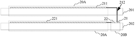
- FIG. 2A and FIG. 2B are schematic diagrams showing the structure of two display panels according to an embodiment of the present invention.
- the display panel includes: a first transparent substrate 201 and a second transparent substrate 202 disposed opposite to each other, and a first transparent substrate
- the first transparent substrate 201 and the second transparent substrate 202 each include a display area 20A.
- the display area 20A of the first transparent substrate 201 is provided with a touch electrode 211 and a display area of the second transparent substrate 202.
- a display electrode 221 is provided in 20A.
- a via 212 is formed in the first transparent substrate 201.
- the first transparent substrate 201 or the second transparent substrate 202 is further provided with a bonding area 20B located around the display area 20A, and the bonding area 20B shown in FIG. 2A is located on the second transparent substrate 202, as shown in FIG. 2B.
- the region 20B is located on the first transparent substrate 201.
- a first bonding terminal 21 connected to the touch electrode 211 and a second bonding terminal 22 connected to the display electrode 221 are disposed in the bonding area 20B, and when the bonding area 20B is located on the first transparent substrate 201, The hole 212 is used to connect the second bonding terminal 22 and the display electrode 221; or, when the bonding region 20B is located on the second transparent substrate 202, the via 212 is used to connect the first bonding terminal 21 and the touch electrode 211.
- the touch panel 211 is disposed in the display area 20A on the side of the first transparent substrate 201 facing away from the second transparent substrate 202, and the display area 20A on the side of the second transparent substrate 202 facing the first transparent substrate 201 is disposed.
- the first bonding terminal 21 and the second bonding terminal 22 are generally arranged side by side, and the connecting lines are parallel to the side close to the transparent substrate ( As shown in Figures 3A and 3B).
- the touch electrode 211 and the display electrode 221 each include a plurality of electrodes.
- the display electrode 221 includes a gate and a source and a drain, and the gate and the source and drain are layered.
- the display electrode An anode and a cathode are included, and the anode and cathode are layered.
- the first bonding terminal and the second bonding terminal are respectively connected in the bonding area of the first transparent substrate or the second transparent substrate, and the first bonding terminal and the second bonding terminal are respectively connected to the touch
- the electrode and the display electrode since the first bonding terminal and the second bonding terminal are all located on the same transparent substrate, can be bonded to the flexible circuit board at the same time, without requiring two bonding, reducing the number of bonding, Save time and effort; at the same time, since the first bonding terminal and the second bonding terminal are all located on the same transparent substrate, the FPC that is bonded to the bonding terminal of the touch electrode does not need to connect the bonding terminal and the PCB across the layer, thereby solving the problem.
- the via 212 is formed on the periphery of the sealant of the display panel, and thus After the frame sealant is finished, a through hole is opened. Further, in the LCD, after the touch electrode is completed and the polarizer is completed, the via hole is opened.
- the touch electrode and the display electrode each include a lead wire, and the touch electrode or the display electrode is connected to the bonding terminal through a wire, or the bonding terminal is connected through the wire and the via hole.
- FIG. 3A is a plan view of a first transparent substrate according to an embodiment of the present invention
- FIG. 3B is a top view of a second transparent substrate according to an embodiment of the present invention.
- the first bonding terminal 21 is connected to the printed circuit board 24 through one of the two flexible circuit boards 23, and the second bonding terminal 22 is passed through two flexible portions.
- Another flexible circuit board 23 in the circuit board 23 is connected to the printed circuit board 24.
- a plurality of first bonding terminals 21 and a plurality of second bonding terminals 22 may be disposed in the bonding area (only one first bonding terminal 21 and one second bonding terminal are shown in FIG. 3A). 22), the plurality of first bonding terminals 21 may be connected to the printed circuit board 24 through a flexible circuit board 23, and the plurality of second bonding terminals 22 may be connected to the printed circuit board 24 through another flexible circuit board 23. At this time, the distance between the plurality of first bonding terminals 21 and the plurality of second bonding terminals 22 on the side close to each other may be greater than 100 mm, and the two flexible circuit boards 23 may also be connected to the printed circuit board 24 as a single piece.
- the first bonding terminal 21 and the second bonding terminal 22 are connected to the printed circuit board 24 through the same flexible circuit board 23.
- the use of a FPC for bonding simplifies the bonding operation; and reduces the chance of incoming material curling and improves the mass production yield.
- the distance between the first bonding terminal 21 and the second bonding terminal 22 is less than a predetermined value, so that bonding can be performed by one FPC.
- a plurality of first bonding terminals 21 and a plurality of second bonding terminals 22 may be disposed in the bonding area (only one first bonding terminal 21 and one second bonding terminal are shown in FIG. 3B). 22), the plurality of first bonding terminals 21 and the plurality of second bonding terminals 22 may be connected to the printed circuit board 24 through the same flexible circuit board 23. At this time, the distance between the plurality of first bonding terminals 21 and the plurality of second bonding terminals 22 on the side close to each other may be greater than or equal to 100 micrometers and less than or equal to 100 millimeters, and the two flexible circuit boards 23 may also be The printed circuit board 24 is connected as a single piece.
- the embodiment of the invention further provides a display device comprising a display panel as shown in any of FIGS. 2A-3B.
- the display device may be any product having a display function, such as a mobile phone, a tablet computer, a television, a display, a notebook computer, a digital photo frame, a navigator, or the like. component.
- the display can be an LCD or an OLED display.
- a first bonding terminal and a second bonding terminal are disposed in a bonding area of the first transparent substrate or the second transparent substrate, and the first bonding terminal and the second bonding terminal are respectively connected to the touch electrode
- the bonding can be performed simultaneously with the flexible circuit board, without requiring two bonding, reducing the number of bonding, saving
- the FPC that is bonded to the bonding terminal of the touch electrode does not need to connect the bonding terminal and the PCB across the layer, thereby solving the amount.
- FIG. 4 is a flowchart of a bonding method according to an embodiment of the present invention. Referring to FIG. 4, the method includes:
- Step 301 Provide a display panel.
- FIG. 5A and FIG. 5B are schematic diagrams showing the structure of two display panels provided in step 301.
- the display panel includes a first transparent substrate 201 and a second transparent substrate 202.
- the first transparent substrate 201 is located on the light emitting side of the display panel.
- the transparent substrate 201 and the second transparent substrate 202 each include a display area 20A, the display area 20A of the first transparent substrate 201 is provided with a touch electrode 211, and the display area 20A of the second transparent substrate 202 is provided with a display electrode 221;
- the first transparent substrate 201 or the second transparent substrate 202 is further provided with a bonding area 20B located around the display area 20A, and the bonding area 20B shown in FIG. 5A is located on the second transparent substrate 202, as shown in FIG. 5B.
- the region 20B is located on the first transparent substrate 201.
- the first bonding terminal 21 and the second bonding terminal 22 are provided in the bonding area 20B.
- the touch panel 211 is disposed in the display area 20A on the side of the first transparent substrate 201 facing away from the second transparent substrate 202, and the display area 20A on the side of the second transparent substrate 202 facing the first transparent substrate 201 is disposed.
- the display panel further includes a lead 20 connecting the touch electrode 211 and the display electrode 221 , and the touch electrode 211 or the display electrode 221 can be connected to the bonding terminal through the lead 20 .
- the second transparent substrate 202 is provided with a bonding region 20B, and the display electrode 221 is connected to the second bonding terminal 22 through the lead 20.
- the remaining first bonding terminal 21 (at this time, the first bonding)
- the terminal 21 is a remaining bonding terminal) and the touch electrode 211 (where the touch electrode is the remaining electrode) is not connected.
- FIG. 5A the second transparent substrate 202 is provided with a bonding region 20B, and the display electrode 221 is connected to the second bonding terminal 22 through the lead 20.
- the first transparent substrate 201 is provided with a bonding region 20B, and the touch electrode 211 is connected to the first bonding terminal 21 through the lead 20.
- the remaining second bonding terminal 22 (at this time, the second state) Fixed terminal 22 is the remaining bonding terminal) and the display electrode 221 (the display electrode is the remaining electrode at this time) is not connected.
- Step 302 Opening a via hole on the first transparent substrate.
- the step 302 may include: forming a via hole on the first transparent substrate by using laser drilling, so as to easily and conveniently provide a via hole on the first transparent substrate.
- the structure is as shown in FIG. 6A, and the first transparent substrate 201 is provided with a via hole 212.
- the structure is as shown in FIG. 6B, and the first transparent substrate 201 is provided with a via hole 212.
- the via 212 is disposed corresponding to one end of the lead 20 extending to facilitate subsequent connection of the electrode and the bonding terminal.
- Step 303 connect the remaining bonding terminal and the remaining electrode through the via.
- step 303 the remaining bonding terminals of the first bonding terminal 21 and the second bonding terminal 22 may be connected to the remaining electrodes through the via holes.
- the via 212 may be located on the first transparent substrate 201, and the first bonding terminal 21 may be passed through the via 212 in step 303 (remaining The bonding terminal is connected to the touch electrode 211 (remaining electrode). As shown in FIG. 6A, when the bonding region 20B is located on the second transparent substrate 202, the via 212 may be located on the first transparent substrate 201, and the first bonding terminal 21 may be passed through the via 212 in step 303 (remaining The bonding terminal is connected to the touch electrode 211 (remaining electrode). As shown in FIG.
- the via 212 when the bonding region 20B is located on the first transparent substrate 201, the via 212 may be located on the first transparent substrate 201, and in step 303, the second bonding terminal 22 may be passed through the via 212 (remaining The bonding terminal) is connected to the display electrode 221 (remaining electrode).
- step 303 may include:
- a conductive paste is injected into the via hole to connect the second bonding terminal and the display electrode, or to connect the first bonding terminal and the touch electrode.
- Conductive glue is used for through-hole connection, which is convenient to manufacture.
- the conductive paste may be a silver paste.
- a conductive paste is injected into the via 212 to form a wiring, and the first bonding terminal 21 and the touch electrode 211 are connected (see FIG. 2A), or the second bonding terminal 22 and the display electrode 221 are connected (see FIG. 2B). Specifically, the line formed by the conductive paste is used to connect the first bonding terminal 21 and the lead 20 of the touch electrode 211, or the second bonding terminal 22 and the lead 20 of the display electrode 221.
- Step 304 Bonding the first bonding terminal and the second bonding terminal to the flexible circuit board at the same time.
- step 304 may include:
- Anisotropic Conductive Films are applied in the bonding area; the first bonding terminal and the second bonding terminal are passed through an anisotropic conductive adhesive (also called an anisotropic conductive adhesive). At the same time, it is aligned with the flexible circuit board.
- anisotropic conductive adhesive also called an anisotropic conductive adhesive
- the first bonding terminal and the second bonding terminal are both disposed in the same transparent On the substrate, the first bonding terminal and the second bonding terminal can be simultaneously bonded to the flexible circuit board to solve the problem caused by the number of bonding times.
- the first bonding terminal and the second bonding terminal may be respectively associated with two flexible circuit boards, and reference may be made to FIG. 3A.
- two FPCs for bonding you can take advantage of the existing design of FPC.
- the first bonding terminal and the second bonding terminal are bonded to the same flexible circuit board, and reference may be made to FIG. 3B.
- the use of a FPC for bonding simplifies the bonding operation; and reduces the chance of FPC incoming material curling and improves the mass production yield.
- a first bonding terminal and a second bonding terminal are disposed in a bonding area of the first transparent substrate or the second transparent substrate, and the first bonding terminal and the second bonding terminal are respectively connected to the touch electrode
- the bonding can be performed simultaneously with the flexible circuit board, without requiring two bonding, reducing the number of bonding, saving
- the FPC that is bonded to the bonding terminal of the touch electrode does not need to connect the bonding terminal and the PCB across the layer, thereby solving the amount.
Landscapes
- Physics & Mathematics (AREA)
- Nonlinear Science (AREA)
- Engineering & Computer Science (AREA)
- General Physics & Mathematics (AREA)
- Mathematical Physics (AREA)
- Chemical & Material Sciences (AREA)
- Crystallography & Structural Chemistry (AREA)
- Optics & Photonics (AREA)
- Manufacturing & Machinery (AREA)
- Microelectronics & Electronic Packaging (AREA)
- Theoretical Computer Science (AREA)
- Computer Hardware Design (AREA)
- Human Computer Interaction (AREA)
- General Engineering & Computer Science (AREA)
- Devices For Indicating Variable Information By Combining Individual Elements (AREA)
- Liquid Crystal (AREA)
Abstract
Description
本申请要求于2017年2月8日提交中国专利局、申请号为201710072174.2、发明名称为“显示基板、显示面板、显示装置及邦定方法”的中国专利申请的优先权,其全部内容通过引用结合在本申请中。This application claims the priority of the Chinese Patent Application filed on February 8, 2017, the Chinese Patent Office, the application number is 201710072174.2, the name of the invention is "display substrate, display panel, display device and bonding method", the entire contents of which are incorporated by reference. Combined in this application.
本申请涉及显示领域,特别涉及一种显示基板、显示面板、显示装置及邦定方法。The present application relates to the field of display, and in particular to a display substrate, a display panel, a display device, and a bonding method.
显示器是一种显示装置,邦定(英文Bonding),也称绑定,是指在显示器的生产过程中,将面板(英文Panel)和柔性电路板(英文Flexible Printed Circuit,简称FPC),或FPC和印刷电路板(英文Printed CircuitBoard,简称PCB)通过各向异性导电胶(英文Anisotropic Conductive Film,简称ACF)按照一定的工作流程组合到一起并导通的过程,是显示器模组工厂普遍采用的工艺。The display is a display device, Bonding, also known as binding, refers to the panel (English Panel) and flexible circuit board (English Flexible Printed Circuit, FPC for short), or FPC in the production process of the display. And printed circuit board (English Printed Circuit Board, referred to as PCB) through anisotropic conductive adhesive (Anisotropic Conductive Film, ACF) according to a certain workflow combined and conductive process, is commonly used in display module factory .
但是,对于外挂式触控(英文On Cell Touch)显示面板而言,在进行面板和FPC的邦定时,除了要将面板中显示电极的邦定端子(英文Pad)与FPC进行邦定外,还需要将面板中触控电极的邦定端子与FPC进行邦定。以液晶显示面板为例,显示面板包括间隔设置的第一透明基板和第二透明基板,所述第一透明基板位于所述显示面板的出光侧,第二透明基板包括显示区域和位于显示区域周边的邦定区域,所述第二透明基板的显示区域设有显示电极,显示电极的邦定端子设置在第二透明基板的邦定区域内;第一透明基板包括显示区域和位于显示区域周边的邦定区域,所述第一透明基板的显示区域设有触控电极,触控电极的邦定端子设置在第一透明基板的邦定区域内。However, for the On-Touch (English On Cell Touch) display panel, in addition to the bonding of the panel and the FPC, the bonding terminal (English Pad) of the display panel in the panel is bonded to the FPC. The bonding terminal of the touch electrode in the panel needs to be bonded to the FPC. Taking the liquid crystal display panel as an example, the display panel includes a first transparent substrate and a second transparent substrate, the first transparent substrate is located on the light emitting side of the display panel, and the second transparent substrate includes a display area and is located around the display area. a bonding area, a display area of the second transparent substrate is provided with a display electrode, and a bonding terminal of the display electrode is disposed in a bonding area of the second transparent substrate; the first transparent substrate includes a display area and a periphery of the display area In the bonding area, the display area of the first transparent substrate is provided with a touch electrode, and the bonding terminal of the touch electrode is disposed in a bonding area of the first transparent substrate.
由于显示电极的邦定端子和触控电极的邦定端子处于不同层,需要采用两块FPC分别与处于不同层的邦定端子进行邦定操作,一方面FPC与邦定端子的邦定次数多,费时费力,另外一方面,由于PCB通常与第二透明基板同层设置,与触控电极的邦定端子邦定的FPC需要跨层连接邦定端子和PCB的原因,导致目前量产良率较低。 Since the bonding terminal of the display electrode and the bonding terminal of the touch electrode are in different layers, it is necessary to use two FPCs to perform bonding operation with the bonding terminals at different layers respectively, and on the one hand, the bonding times of the FPC and the bonding terminal are many. It takes time and effort. On the other hand, since the PCB is usually disposed in the same layer as the second transparent substrate, the FPC that is bonded to the bonding terminal of the touch electrode needs to connect the bonding terminal and the PCB across the layer, resulting in the current mass production yield. Lower.
发明内容Summary of the invention
本发明实施例提供了一种显示基板、显示面板、显示装置及邦定方法,可以解决现有外挂式触控显示面板进行邦定时,邦定次数多,费时费力,且量产良率较低的问题,所述技术方案如下:The embodiment of the invention provides a display substrate, a display panel, a display device and a bonding method, which can solve the state of the existing external touch display panel, the number of bonding times is large, time-consuming and laborious, and the mass production yield is low. The technical solution is as follows:
第一方面,本发明实施例提供了一种显示基板,所述显示基板包括:透明基板,所述透明基板包括显示区域,以及位于所述显示区域周边的邦定区域;In a first aspect, an embodiment of the present invention provides a display substrate, the display substrate includes: a transparent substrate, the transparent substrate includes a display area, and a bonding area located around the display area;
所述邦定区域设有与触控电极连接的第一邦定端子,和与显示电极连接的第二邦定端子,所述触控电极和所述显示电极中的一个电极位于所述显示区域内,另一个电极位于另一透明基板上,所述另一透明基板与所述透明基板相对设置。The bonding region is provided with a first bonding terminal connected to the touch electrode, and a second bonding terminal connected to the display electrode, and one of the touch electrode and the display electrode is located in the display region The other electrode is located on another transparent substrate, and the other transparent substrate is disposed opposite to the transparent substrate.
在本发明实施例的一种实现方式中,所述显示基板为阵列基板,所述显示电极设置在所述透明基板上。In an implementation manner of the embodiment of the present invention, the display substrate is an array substrate, and the display electrode is disposed on the transparent substrate.
在本发明实施例的另一种实现方式中,所述显示基板为彩膜基板,所述触控电极设置在所述透明基板上,所述彩膜基板上还设有过孔,所述过孔用于连接所述显示电极和所述第二邦定端子。In another implementation manner of the embodiment of the present invention, the display substrate is a color film substrate, the touch electrode is disposed on the transparent substrate, and the color film substrate is further provided with a through hole. A hole is used to connect the display electrode and the second bonding terminal.
第二方面,本发明实施例还提供了一种显示面板,所述显示面板包括:相对设置的第一透明基板和第二透明基板,所述第一透明基板位于所述显示面板的出光侧,所述第一透明基板和第二透明基板均包括显示区域,所述第一透明基板的显示区域内设有触控电极,所述第二透明基板的显示区域内设有显示电极;In a second aspect, the embodiment of the present invention further provides a display panel, the display panel includes: a first transparent substrate and a second transparent substrate disposed opposite to each other, the first transparent substrate is located on a light emitting side of the display panel, Each of the first transparent substrate and the second transparent substrate includes a display area, a touch electrode is disposed in the display area of the first transparent substrate, and a display electrode is disposed in the display area of the second transparent substrate;
所述第一透明基板上开设过孔;a through hole is formed in the first transparent substrate;
所述第一透明基板或所述第二透明基板上还设有位于所述显示区域周边的邦定区域,所述邦定区域内设有与触控电极连接的第一邦定端子和与显示电极连接的第二邦定端子;The first transparent substrate or the second transparent substrate is further provided with a bonding area around the display area, and the first bonding terminal and the display connected to the touch electrode are disposed in the bonding area. a second bonding terminal connected to the electrode;
其中,当所述第一透明基板上设有所述邦定区域时,所述过孔用于连接所述第二邦定端子和所述显示电极;当所述第二透明基板上设有所述邦定区域时,所述过孔用于连接所述第一邦定端子和所述触控电极。Wherein, when the bonding region is disposed on the first transparent substrate, the via hole is used to connect the second bonding terminal and the display electrode; when the second transparent substrate is provided The via hole is used to connect the first bonding terminal and the touch electrode when the bonding region is described.
在本发明实施例的一种实现方式中,所述显示面板还包括:印刷电路板和两块柔性电路板,所述第一邦定端子通过所述两块柔性电路板中的一块柔性电路板与印刷电路板连接,所述第二邦定端子通过所述两块柔性电路板中的另一块柔性电路板与印刷电路板连接。 In an implementation manner of the embodiment of the present invention, the display panel further includes: a printed circuit board and two flexible circuit boards, wherein the first bonding terminal passes through one of the two flexible circuit boards Connected to the printed circuit board, the second bonding terminal is connected to the printed circuit board by another of the two flexible circuit boards.
在本发明实施例的另一种实现方式中,所述邦定区域设置有多个第一邦定端子和多个第二邦定端子,所述多个第一邦定端子通过所述一块柔性电路板与印刷电路板连接,所述多个第二邦定端子通过所述另一块柔性电路板与所述印刷电路板连接。In another implementation manner of the embodiment of the present invention, the bonding area is provided with a plurality of first bonding terminals and a plurality of second bonding terminals, and the plurality of first bonding terminals pass the piece of flexible The circuit board is coupled to the printed circuit board, and the plurality of second bonding terminals are coupled to the printed circuit board by the other flexible circuit board.
在本发明实施例的另一种实现方式中,当所述多个第一邦定端子和所述多个第二邦定端子通过两块柔性电路板与印刷电路板连接时,所述多个第一邦定端子和所述多个第二邦定端子相互靠近一侧的距离大于100毫米。In another implementation manner of the embodiment of the present invention, when the plurality of first bonding terminals and the plurality of second bonding terminals are connected to the printed circuit board through two flexible circuit boards, the plurality of The first bonding terminal and the plurality of second bonding terminals are closer to each other by a distance greater than 100 mm.
在本发明实施例的另一种实现方式中,所述两块柔性电路板与所述印刷电路板连接为一体件。In another implementation manner of the embodiment of the present invention, the two flexible circuit boards are connected to the printed circuit board as a single piece.
在本发明实施例的另一种实现方式中,所述显示面板还包括:印刷电路板和一块柔性电路板,所述第一邦定端子和所述第二邦定端子通过同一块柔性电路板与印刷电路板连接。In another implementation manner of the embodiment of the present invention, the display panel further includes: a printed circuit board and a flexible circuit board, wherein the first bonding terminal and the second bonding terminal pass through the same flexible circuit board Connect to a printed circuit board.
在本发明实施例的另一种实现方式中,所述邦定区域设置有多个第一邦定端子和多个第二邦定端子,所述多个第一邦定端子和所述多个第二邦定端子均通过同一块柔性电路板与所述印刷电路板连接。In another implementation manner of the embodiment of the present invention, the bonding area is provided with a plurality of first bonding terminals and a plurality of second bonding terminals, the plurality of first bonding terminals and the plurality of The second bonding terminals are all connected to the printed circuit board through the same flexible circuit board.
在本发明实施例的另一种实现方式中,当所述多个第一邦定端子和所述多个第二邦定端子通过同一块柔性电路板与印刷电路板连接时,所述多个第一邦定端子和所述多个第二邦定端子相互靠近一侧距离大于或等于100微米,且小于或等于100毫米。In another implementation manner of the embodiment of the present invention, when the plurality of first bonding terminals and the plurality of second bonding terminals are connected to the printed circuit board through the same flexible circuit board, the plurality of The first bonding terminal and the plurality of second bonding terminals are closer to each other by a distance greater than or equal to 100 micrometers and less than or equal to 100 millimeters.
在本发明实施例的另一种实现方式中,所述同一块柔性电路板和所述印刷电路板连接为一体件。In another implementation manner of the embodiment of the present invention, the same flexible circuit board and the printed circuit board are connected as a single piece.
在本发明实施例的另一种实现方式中,所述显示面板为液晶显示器LCD或有机发光二极管OLED显示器的显示面板。In another implementation manner of the embodiment of the present invention, the display panel is a display panel of a liquid crystal display LCD or an organic light emitting diode OLED display.
第三方面,本发明实施例还提供了一种显示装置,所述显示装置包括如第二方面任一项所述的显示面板。In a third aspect, the embodiment of the present invention further provides a display device, comprising the display panel according to any one of the second aspects.
第四方面,本发明实施例还提供了一种邦定方法,所述方法包括:In a fourth aspect, an embodiment of the present invention further provides a bonding method, where the method includes:
提供一显示面板,所述显示面板包括相对设置的第一透明基板和第二透明基板,所述第一透明基板位于所述显示面板的出光侧,所述第一透明基板和第二透明基板均包括显示区域,所述第一透明基板的显示区域内设有触控电极,所述第二透明基板的显示区域内设有显示电极;所述第一透明基板或所述第二透明基板上还设有位于所述显示区域周边的邦定区域,所述邦定区域内设有第 一邦定端子和第二邦定端子;当所述第一透明基板设有所述邦定区域时,所述第一邦定端子和所述触控电极连接,当所述第二透明基板设有所述邦定区域时,所述第二邦定端子和所述显示电极连接;Providing a display panel, the display panel includes a first transparent substrate and a second transparent substrate, the first transparent substrate is located on a light emitting side of the display panel, and the first transparent substrate and the second transparent substrate are both The display area includes a touch electrode, and the display area of the second transparent substrate is provided with a display electrode; the first transparent substrate or the second transparent substrate is further There is a bonding area located around the display area, and the bonding area is provided with a bonding terminal and a second bonding terminal; when the first transparent substrate is provided with the bonding region, the first bonding terminal is connected to the touch electrode, and when the second transparent substrate is disposed The second bonding terminal is connected to the display electrode when the bonding region is present;
在第一透明基板上开设过孔;Opening a via hole on the first transparent substrate;
通过所述过孔连接剩余邦定端子和剩余电极,其中,当所述第一透明基板设有所述邦定区域时,所述剩余邦定端子为所述第二邦定端子,所述剩余电极为所述显示电极,当所述第二透明基板设有所述邦定区域时,所述剩余邦定端子为所述第一邦定端子,所述剩余电极为所述触控电极;Connecting the remaining bonding terminal and the remaining electrode through the via hole, wherein when the first transparent substrate is provided with the bonding region, the remaining bonding terminal is the second bonding terminal, and the remaining The electrode is the display electrode, when the second transparent substrate is provided with the bonding region, the remaining bonding terminal is the first bonding terminal, and the remaining electrode is the touch electrode;
将第一邦定端子和第二邦定端子同时与柔性电路板进行邦定。The first bonding terminal and the second bonding terminal are simultaneously bonded to the flexible circuit board.
在本发明实施例的一种实现方式中,所述在第一透明基板上开设过孔,包括:In an implementation manner of the embodiment of the present invention, the opening a via hole on the first transparent substrate includes:
采用激光打孔的方式在第一透明基板上开设过孔。A via hole is formed in the first transparent substrate by laser drilling.
在本发明实施例的另一种实现方式中,所述通过所述过孔连接剩余邦定端子和剩余电极,包括:In another implementation manner of the embodiment of the present invention, the connecting the remaining bonding terminal and the remaining electrode through the via hole includes:
在所述过孔内注入导电胶,以连接所述剩余邦定端子和所述剩余电极。A conductive paste is injected into the via to connect the remaining bonding terminal and the remaining electrode.
在本发明实施例的另一种实现方式中,所述导电胶为银胶。In another implementation manner of the embodiment of the present invention, the conductive adhesive is a silver paste.
在本发明实施例的另一种实现方式中,所述将第一邦定端子和第二邦定端子同时与柔性电路板进行邦定,包括:In another implementation manner of the embodiment of the present invention, the bonding the first bonding terminal and the second bonding terminal to the flexible circuit board at the same time, including:
在所述邦定区域内涂敷各向异性导电胶;Coating an anisotropic conductive paste in the bonding region;
通过各向异性导电胶,将第一邦定端子和第二邦定端子同时与柔性电路板进行对位压合。The first bonding terminal and the second bonding terminal are simultaneously aligned with the flexible circuit board by an anisotropic conductive adhesive.
在本发明实施例的另一种实现方式中,所述第一邦定端子和第二邦定端子分别与两块柔性电路板进行邦定。In another implementation manner of the embodiment of the present invention, the first bonding terminal and the second bonding terminal respectively perform bonding with two flexible circuit boards.
在本发明实施例的另一种实现方式中,所述第一邦定端子和第二邦定端子与同一块柔性电路板进行邦定。In another implementation of the embodiment of the present invention, the first bonding terminal and the second bonding terminal are bonded to the same flexible circuit board.
本发明实施例提供的技术方案带来的有益效果是:The beneficial effects brought by the technical solutions provided by the embodiments of the present invention are:
在显示基板的透明基板的邦定区域内设置第一邦定端子和第二邦定端子,第一邦定端子和第二邦定端子分别连接触控电极和显示电极,由于第一邦定端子和第二邦定端子均位于显示基板的透明基板上,因此可以同时与柔性电路板进行邦定,而不需要进行两次邦定,减少了邦定次数,省时省力;同时,由于第一邦定端子和第二邦定端子均位于显示基板的透明基板上,与触控电极的邦 定端子邦定的FPC不需要跨层连接邦定端子和PCB,解决了量产良率低的问题。a first bonding terminal and a second bonding terminal are disposed in a bonding area of the transparent substrate of the display substrate, and the first bonding terminal and the second bonding terminal are respectively connected to the touch electrode and the display electrode, because the first bonding terminal And the second bonding terminal is located on the transparent substrate of the display substrate, so that the bonding can be performed simultaneously with the flexible circuit board, without requiring two bonding, reducing the number of bonding, saving time and labor; meanwhile, due to the first The bonding terminal and the second bonding terminal are both located on the transparent substrate of the display substrate, and the state of the touch electrode The FPC of the terminal bonding does not need to connect the bonding terminal and the PCB across the layer, which solves the problem of low yield of mass production.
为了更清楚地说明本发明实施例中的技术方案,下面将对实施例描述中所需要使用的附图作简单地介绍,显而易见地,下面描述中的附图仅仅是本申请的一些实施例,对于本领域普通技术人员来讲,在不付出创造性劳动的前提下,还可以根据这些附图获得其他的附图。In order to more clearly illustrate the technical solutions in the embodiments of the present invention, the drawings used in the description of the embodiments will be briefly described below. It is obvious that the drawings in the following description are only some embodiments of the present application. Other drawings may also be obtained from those of ordinary skill in the art in light of the inventive work.
图1是本发明实施例提供的一种显示基板的结构示意图;1 is a schematic structural diagram of a display substrate according to an embodiment of the present invention;
图2A和图2B是本发明实施例提供的两种显示面板的结构示意图;2A and 2B are schematic structural diagrams of two display panels provided by an embodiment of the present invention;
图3A是本发明实施例提供的第一透明基板的俯视图;3A is a top plan view of a first transparent substrate according to an embodiment of the present invention;
图3B是本发明实施例提供的第二透明基板的俯视图;FIG. 3B is a top view of a second transparent substrate according to an embodiment of the present invention; FIG.
图4是本发明实施例提供的一种邦定方法的流程图;4 is a flowchart of a bonding method according to an embodiment of the present invention;
图5A和图5B是本发明实施例提供的显示面板在进行邦定的过程中的结构示意图;FIG. 5A and FIG. 5B are schematic diagrams showing the structure of a display panel according to an embodiment of the present invention;
图6A和图6B是本发明实施例提供的显示面板在进行邦定的过程中的结构示意图。6A and FIG. 6B are schematic diagrams showing the structure of a display panel in a bonding process according to an embodiment of the present invention.
为使本申请的目的、技术方案和优点更加清楚,下面将结合附图对本发明实施方式作进一步地详细描述。The embodiments of the present invention will be further described in detail below with reference to the accompanying drawings.
图1是本发明实施例提供的一种显示基板的结构示意图,参见图1,显示基板包括:透明基板100,透明基板100包括显示区域101,以及位于显示区域101周边的邦定区域102。1 is a schematic structural diagram of a display substrate according to an embodiment of the present invention. Referring to FIG. 1 , the display substrate includes a
邦定区域102设有与触控电极连接的第一邦定端子11,和与显示电极连接的第二邦定端子12,触控电极和显示电极中的一个电极位于显示区域101内,另一个电极位于另一透明基板100上,另一透明基板与透明基板100相对设置。The
在该显示基板中,在显示基板的透明基板的邦定区域内设置第一邦定端子和第二邦定端子,第一邦定端子和第二邦定端子分别连接触控电极和显示电极,由于第一邦定端子和第二邦定端子均位于显示基板的透明基板上,因此可以同时与柔性电路板进行邦定,而不需要进行两次邦定,减少了邦定次数,省 时省力;同时,由于第一邦定端子和第二邦定端子均位于显示基板的透明基板上,与触控电极的邦定端子邦定的FPC不需要跨层连接邦定端子和PCB,解决了量产良率低的问题。In the display substrate, a first bonding terminal and a second bonding terminal are disposed in a bonding area of the transparent substrate of the display substrate, and the first bonding terminal and the second bonding terminal are respectively connected to the touch electrode and the display electrode, Since the first bonding terminal and the second bonding terminal are both located on the transparent substrate of the display substrate, the bonding can be performed simultaneously with the flexible circuit board, without requiring two bonding, reducing the number of bonding, saving At the same time, since the first bonding terminal and the second bonding terminal are both located on the transparent substrate of the display substrate, the FPC that is bonded to the bonding terminal of the touch electrode does not need to connect the bonding terminal and the PCB across the layer to solve the problem. The problem of low yield of mass production.
其中,触控电极设置在透明基板100背向另一透明基板的一面上,或者,显示电极设置在透明基板100面向另一透明基板的一面上。根据触控电极设置在透明基板100背向另一透明基板的一面上,显示电极位于另一透明基板上;或者显示电极设置在透明基板100面向另一透明基板的一面上,触控电极位于另一透明基板上;可以看出,触控电极和显示电极分别设置在两个不同的透明基板上,该显示基板应用在外挂式触控显示面板中。The touch electrode is disposed on a side of the
在本发明实施例中,第一邦定端子11的数量可以根据触控电极的数量设置,第二邦定端子12的数量可以根据显示电极的数量设置。In the embodiment of the present invention, the number of the
在本发明实施例中,显示基板可以为液晶显示器(英文Liquid Crystal Display,简称LCD)的阵列基板或者彩膜基板,显示基板还可以是有机发光二极管(Organic Light-Emitting Diode,简称OLED)显示器的阵列基板或者上透明基板(盖板)。In the embodiment of the present invention, the display substrate may be an array substrate or a color filter substrate of a liquid crystal display (LCD), and the display substrate may also be an organic light-emitting diode (OLED) display. Array substrate or upper transparent substrate (cover).
在液晶显示器中,将邦定区域设置在阵列基板或者彩膜基板上,都需要在彩膜基板上开设过孔,以连接邦定端子和与邦定区域处于不同透明基板的电极。在OLED显示器中,将邦定区域设置在阵列基板或者OLED显示器的上透明基板上,都需要在OLED显示器的上透明基板上开设过孔,以连接邦定端子和与邦定区域处于不同透明基板的电极。In the liquid crystal display, the bonding region is disposed on the array substrate or the color film substrate, and a via hole is formed on the color filter substrate to connect the bonding terminal and the electrode on the transparent substrate different from the bonding region. In an OLED display, the bonding region is disposed on the array substrate or the upper transparent substrate of the OLED display, and a via hole is formed on the upper transparent substrate of the OLED display to connect the bonding terminal and the transparent substrate different from the bonding region. Electrode.
在一种可能的实现方式中,显示基板为阵列基板,既可以是LCD的阵列基板,也可以是OLED显示器的阵列基板,显示电极设置在透明基板上。此时,触控电极位于LCD的彩膜基板的透明基板上或者OLED显示器的上透明基板上,由于阵列基板上的显示电极的邦定端子多于触控电极的邦定端子,也即显示电极连接的第一邦定端子多于触控电极连接的第二邦定端子,且过孔数量与需要连接的邦定端子数量相当,因此将邦定区域设置在阵列基板上,可以减少过孔设置。In one possible implementation manner, the display substrate is an array substrate, which may be an array substrate of an LCD or an array substrate of an OLED display, and the display electrodes are disposed on the transparent substrate. At this time, the touch electrode is located on the transparent substrate of the color filter substrate of the LCD or the upper transparent substrate of the OLED display, because the bonding terminal of the display electrode on the array substrate is more than the bonding terminal of the touch electrode, that is, the display electrode The first bonding terminal connected is more than the second bonding terminal connected to the touch electrode, and the number of vias is equivalent to the number of bonding terminals to be connected, so the bonding area is set on the array substrate, and the via setting can be reduced. .
在另一种可能的实现方式中,显示基板为彩膜基板,彩膜基板上还设有过孔,过孔用于连接显示电极和第二邦定端子。当邦定区域设置在彩膜基板上时,需要将显示电极通过过孔连接到邦定区域的第二邦定端子。In another possible implementation manner, the display substrate is a color film substrate, and the color film substrate is further provided with a via hole for connecting the display electrode and the second bonding terminal. When the bonding area is disposed on the color filter substrate, the display electrode needs to be connected to the second bonding terminal of the bonding area through the via hole.
与彩膜基板类似,当显示基板为OLED显示器的上透明基板时,OLED显 示器的上透明基板也需要开设过孔。过孔用于连接显示电极和第二邦定端子。Similar to the color film substrate, when the display substrate is an upper transparent substrate of the OLED display, the OLED display The upper transparent substrate of the display also needs to have a via hole. A via is used to connect the display electrode to the second bonding terminal.
图2A和图2B是本发明实施例提供的两种显示面板的结构示意图,参见图2A和图2B,显示面板包括:相对设置的第一透明基板201和第二透明基板202,第一透明基板201位于显示面板的出光侧,第一透明基板201和第二透明基板202均包括显示区域20A,第一透明基板201的显示区域20A内设有触控电极211,第二透明基板202的显示区域20A内设有显示电极221。FIG. 2A and FIG. 2B are schematic diagrams showing the structure of two display panels according to an embodiment of the present invention. Referring to FIG. 2A and FIG. 2B, the display panel includes: a first
第一透明基板201上开设过孔212。第一透明基板201或第二透明基板202上还设有位于显示区域20A周边的邦定区域20B,图2A所示的邦定区域20B位于第二透明基板202上,图2B所示的邦定区域20B位于第一透明基板201上。邦定区域20B内设有与触控电极211连接的第一邦定端子21,和与显示电极221连接的第二邦定端子22,当邦定区域20B位于第一透明基板201上时,过孔212用于连接第二邦定端子22和显示电极221;或者,当邦定区域20B位于第二透明基板202上时,过孔212用于连接第一邦定端子21和触控电极211。A via 212 is formed in the first
具体地,第一透明基板201背向第二透明基板202的一面上的显示区域20A内设有触控电极211,第二透明基板202面向第一透明基板201的一面上的显示区域20A内设有显示电极221。Specifically, the
图2A和图2B仅为示意,一方面,实际制作时,第一邦定端子21和第二邦定端子22通常为并排设置,且二者连线平行于所在透明基板上所靠近的一边(如图3A和图3B所示)。另一方面,触控电极211和显示电极221均包括多个电极,在LCD中,显示电极221包括栅极和源漏极,栅极和源漏极分层设置;在OLED显示器中,显示电极包括阳极和阴极,且阳极和阴极分层设置。2A and 2B are only schematic views. On the one hand, in actual production, the
在该显示面板中,通过在第一透明基板或第二透明基板的邦定区域内设置第一邦定端子和第二邦定端子,第一邦定端子和第二邦定端子分别连接触控电极和显示电极,由于第一邦定端子和第二邦定端子均位于同一透明基板上,因此可以同时与柔性电路板进行邦定,而不需要进行两次邦定,减少了邦定次数,省时省力;同时,由于第一邦定端子和第二邦定端子均位于同一透明基板上,与触控电极的邦定端子邦定的FPC不需要跨层连接邦定端子和PCB,解决了量产良率低的问题。In the display panel, the first bonding terminal and the second bonding terminal are respectively connected in the bonding area of the first transparent substrate or the second transparent substrate, and the first bonding terminal and the second bonding terminal are respectively connected to the touch The electrode and the display electrode, since the first bonding terminal and the second bonding terminal are all located on the same transparent substrate, can be bonded to the flexible circuit board at the same time, without requiring two bonding, reducing the number of bonding, Save time and effort; at the same time, since the first bonding terminal and the second bonding terminal are all located on the same transparent substrate, the FPC that is bonded to the bonding terminal of the touch electrode does not need to connect the bonding terminal and the PCB across the layer, thereby solving the problem. The problem of low yield of mass production.
在本发明实施例中,过孔212开设在显示面板的封框胶外围,因而可以在 封框胶制作完成后开设过孔。进一步地,在LCD中,在触控电极制作完成,且偏光片制作完成后,开设该过孔。In the embodiment of the present invention, the via 212 is formed on the periphery of the sealant of the display panel, and thus After the frame sealant is finished, a through hole is opened. Further, in the LCD, after the touch electrode is completed and the polarizer is completed, the via hole is opened.
在发明实施例中,触控电极和显示电极均包括引线,触控电极或者显示电极通过引线连接邦定端子,或者通过引线和过孔连接邦定端子。In the embodiment of the invention, the touch electrode and the display electrode each include a lead wire, and the touch electrode or the display electrode is connected to the bonding terminal through a wire, or the bonding terminal is connected through the wire and the via hole.
图3A是本发明实施例提供的第一透明基板的俯视图,图3B是本发明实施例提供的第二透明基板的俯视图。参见图3A,在一种可能的实现方式中,第一邦定端子21通过两块柔性电路板23中的一块柔性电路板23与印刷电路板24连接,第二邦定端子22通过两块柔性电路板23中的另一块柔性电路板23与印刷电路板24连接。采用两块FPC进行邦定,可以利用现有设计的FPC。3A is a plan view of a first transparent substrate according to an embodiment of the present invention, and FIG. 3B is a top view of a second transparent substrate according to an embodiment of the present invention. Referring to FIG. 3A, in a possible implementation, the
可选的,邦定区域内可以设置有多个第一邦定端子21和多个第二邦定端子22(图3A中仅示出了一个第一邦定端子21和一个第二邦定端子22),多个第一邦定端子21可以通过一块柔性电路板23与印刷电路板24连接,多个第二邦定端子22可以通过另一块柔性电路板23与印刷电路板24连接。此时,多个第一邦定端子21和多个第二邦定端子22相互靠近一侧的距离可以大于100毫米,该两块柔性电路板23还可以与印刷电路板24连接为一体件。Optionally, a plurality of
参见图3B,在一种可能的实现方式中,第一邦定端子21和第二邦定端子22通过同一块柔性电路板23与印刷电路板24连接。采用一块FPC进行邦定,简化了邦定操作;并且减小了来料卷曲的几率,提高了量产良率。在这种实现方式中,第一邦定端子21和第二邦定端子22距离小于预定值,从而能够通过一块FPC进行邦定。Referring to FIG. 3B, in one possible implementation, the
可选的,邦定区域内可以设置有多个第一邦定端子21和多个第二邦定端子22(图3B中仅示出了一个第一邦定端子21和一个第二邦定端子22),多个第一邦定端子21以及多个第二邦定端子22均可以通过同一块柔性电路板23与印刷电路板24连接。此时,多个第一邦定端子21和多个第二邦定端子22相互靠近一侧的距离可以大于或等于100微米,且小于或等于100毫米,该两块柔性电路板23还可以与印刷电路板24连接为一体件。Optionally, a plurality of
本发明实施例还提供了一种显示装置,显示装置包括如图2A-3B任一所示的显示面板。The embodiment of the invention further provides a display device comprising a display panel as shown in any of FIGS. 2A-3B.
在具体实施时,本发明实施例提供的显示装置可以为手机、平板电脑、电视机、显示器、笔记本电脑、数码相框、导航仪等任何具有显示功能的产品或 部件。示例的,该显示器可以为LCD或者OLED显示器。In a specific implementation, the display device provided by the embodiment of the present invention may be any product having a display function, such as a mobile phone, a tablet computer, a television, a display, a notebook computer, a digital photo frame, a navigator, or the like. component. By way of example, the display can be an LCD or an OLED display.
在该显示装置中,在第一透明基板或第二透明基板的邦定区域内设置第一邦定端子和第二邦定端子,第一邦定端子和第二邦定端子分别连接触控电极和显示电极,由于第一邦定端子和第二邦定端子均位于同一透明基板上,因此可以同时与柔性电路板进行邦定,而不需要进行两次邦定,减少了邦定次数,省时省力;同时,由于第一邦定端子和第二邦定端子均位于同一透明基板上,与触控电极的邦定端子邦定的FPC不需要跨层连接邦定端子和PCB,解决了量产良率低的问题。In the display device, a first bonding terminal and a second bonding terminal are disposed in a bonding area of the first transparent substrate or the second transparent substrate, and the first bonding terminal and the second bonding terminal are respectively connected to the touch electrode And the display electrode, since the first bonding terminal and the second bonding terminal are all located on the same transparent substrate, the bonding can be performed simultaneously with the flexible circuit board, without requiring two bonding, reducing the number of bonding, saving At the same time, since the first bonding terminal and the second bonding terminal are all located on the same transparent substrate, the FPC that is bonded to the bonding terminal of the touch electrode does not need to connect the bonding terminal and the PCB across the layer, thereby solving the amount. The problem of low yield.
图4是本发明实施例提供的一种邦定方法的流程图,参见图4,该方法包括:4 is a flowchart of a bonding method according to an embodiment of the present invention. Referring to FIG. 4, the method includes:
步骤301:提供一显示面板。Step 301: Provide a display panel.
图5A和图5B是步骤301所提供的两种显示面板的结构示意图,显示面板包括相对设置的第一透明基板201和第二透明基板202,第一透明基板201位于显示面板的出光侧,第一透明基板201和第二透明基板202均包括显示区域20A,第一透明基板201的显示区域20A内设有触控电极211,第二透明基板202的显示区域20A内设有显示电极221;FIG. 5A and FIG. 5B are schematic diagrams showing the structure of two display panels provided in
第一透明基板201或第二透明基板202上还设有位于显示区域20A周边的邦定区域20B,图5A所示的邦定区域20B位于第二透明基板202上,图5B所示的邦定区域20B位于第一透明基板201上。邦定区域内20B设有第一邦定端子21和第二邦定端子22。The first
具体地,第一透明基板201背向第二透明基板202的一面上的显示区域20A内设有触控电极211,第二透明基板202面向第一透明基板201的一面上的显示区域20A内设有显示电极221。Specifically, the
如图5A和图5B所示,显示面板还包括连接触控电极211和显示电极221的引线20,触控电极211或者显示电极221可以通过引线20连接邦定端子。如图5A所示,第二透明基板202设有邦定区域20B,显示电极221通过引线20连接第二邦定端子22,此时,剩余的第一邦定端子21(此时第一邦定端子21为剩余邦定端子)和触控电极211(此时触控电极为剩余电极)并未连接。如图5B所示,第一透明基板201设有邦定区域20B,触控电极211通过引线20连接第一邦定端子21,此时,剩余的第二邦定端子22(此时第二邦定端子
22为剩余邦定端子)和显示电极221(此时显示电极为剩余电极)并未连接。As shown in FIG. 5A and FIG. 5B , the display panel further includes a lead 20 connecting the
步骤302:在第一透明基板上开设过孔。Step 302: Opening a via hole on the first transparent substrate.
在本发明实施例中,步骤302可以包括:采用激光打孔的方式在第一透明基板上开设过孔,实现简单方便的在第一透明基板上设置过孔。In the embodiment of the present invention, the
图5A所示的显示面板在开设过孔后,结构如图6A所示,第一透明基板201上开设有过孔212。以图5B所示的显示面板在开设过孔后,结构如图6B所示,第一透明基板201上开设有过孔212。After the via hole is formed in the display panel shown in FIG. 5A, the structure is as shown in FIG. 6A, and the first
进一步地,该过孔212对应引线20伸出的一端设置,从而便于后续连接电极和邦定端子。Further, the via 212 is disposed corresponding to one end of the
步骤303:通过过孔连接剩余邦定端子和剩余电极。Step 303: connect the remaining bonding terminal and the remaining electrode through the via.
在步骤303中,可以将第一邦定端子21和第二邦定端子22中的剩余邦定端子与剩余电极通过过孔进行连接。如图6A所示,当邦定区域20B位于第二透明基板202上时,过孔212可以位于第一透明基板201上,在步骤303中可以通过过孔212将第一邦定端子21(剩余邦定端子)和触控电极211(剩余电极)连接。如图6B所示,当邦定区域20B位于第一透明基板201上时,过孔212可以位于第一透明基板201上,在步骤303中可以通过过孔212将第二邦定端子22(剩余邦定端子)和显示电极221(剩余电极)连接。In
在本发明实施例中,步骤303可以包括:In the embodiment of the present invention, step 303 may include:
在过孔内注入导电胶,以连接第二邦定端子和显示电极,或者连接第一邦定端子和触控电极。采用导电胶进行过孔连接,制作方便。可选的,该导电胶可以为银胶。A conductive paste is injected into the via hole to connect the second bonding terminal and the display electrode, or to connect the first bonding terminal and the touch electrode. Conductive glue is used for through-hole connection, which is convenient to manufacture. Optionally, the conductive paste may be a silver paste.
在过孔212内注入导电胶,形成线路,连接第一邦定端子21和触控电极211(参见图2A),或者连接第二邦定端子22和显示电极221(参见图2B)。具体为,导电胶形成的线路用于连接第一邦定端子21和触控电极211的引线20,或者第二邦定端子22和显示电极221的引线20。A conductive paste is injected into the via 212 to form a wiring, and the
步骤304:将第一邦定端子和第二邦定端子同时与柔性电路板进行邦定。Step 304: Bonding the first bonding terminal and the second bonding terminal to the flexible circuit board at the same time.
在本发明实施例中,步骤304可以包括:In an embodiment of the present invention, step 304 may include:
在邦定区域内涂敷各向异性导电胶(英文Anisotropic Conductive Films,简称ACF);通过各向异性导电胶(也称异方向性导电胶),将第一邦定端子和第二邦定端子同时与柔性电路板进行对位压合。Anisotropic Conductive Films (ACF) are applied in the bonding area; the first bonding terminal and the second bonding terminal are passed through an anisotropic conductive adhesive (also called an anisotropic conductive adhesive). At the same time, it is aligned with the flexible circuit board.
由于本发明实施例中第一邦定端子和第二邦定端子均设置在同一个透明 基板上,因此可以将第一邦定端子和第二邦定端子同时与柔性电路板进行邦定,解决邦定次数多带来的问题。In the embodiment of the invention, the first bonding terminal and the second bonding terminal are both disposed in the same transparent On the substrate, the first bonding terminal and the second bonding terminal can be simultaneously bonded to the flexible circuit board to solve the problem caused by the number of bonding times.
在本发明实施例的一种实现方式中,第一邦定端子和第二邦定端子可以分别与两块柔性电路板进行邦定,可以参照图3A。采用两块FPC进行邦定,可以利用现有设计的FPC。In an implementation manner of the embodiment of the present invention, the first bonding terminal and the second bonding terminal may be respectively associated with two flexible circuit boards, and reference may be made to FIG. 3A. With two FPCs for bonding, you can take advantage of the existing design of FPC.
在本发明实施例的另一种实现方式中,第一邦定端子和第二邦定端子与同一块柔性电路板进行邦定,可以参照图3B。采用一块FPC进行邦定,简化了邦定操作;并且减小了FPC来料卷曲的几率,提高了量产良率。In another implementation of the embodiment of the present invention, the first bonding terminal and the second bonding terminal are bonded to the same flexible circuit board, and reference may be made to FIG. 3B. The use of a FPC for bonding simplifies the bonding operation; and reduces the chance of FPC incoming material curling and improves the mass production yield.
在该显示面板中,在第一透明基板或第二透明基板的邦定区域内设置第一邦定端子和第二邦定端子,第一邦定端子和第二邦定端子分别连接触控电极和显示电极,由于第一邦定端子和第二邦定端子均位于同一透明基板上,因此可以同时与柔性电路板进行邦定,而不需要进行两次邦定,减少了邦定次数,省时省力;同时,由于第一邦定端子和第二邦定端子均位于同一透明基板上,与触控电极的邦定端子邦定的FPC不需要跨层连接邦定端子和PCB,解决了量产良率低的问题。In the display panel, a first bonding terminal and a second bonding terminal are disposed in a bonding area of the first transparent substrate or the second transparent substrate, and the first bonding terminal and the second bonding terminal are respectively connected to the touch electrode And the display electrode, since the first bonding terminal and the second bonding terminal are all located on the same transparent substrate, the bonding can be performed simultaneously with the flexible circuit board, without requiring two bonding, reducing the number of bonding, saving At the same time, since the first bonding terminal and the second bonding terminal are all located on the same transparent substrate, the FPC that is bonded to the bonding terminal of the touch electrode does not need to connect the bonding terminal and the PCB across the layer, thereby solving the amount. The problem of low yield.
以上仅为本发明的可选实施例,并不用以限制本发明,凡在本发明的精神和原则之内,所作的任何修改、等同替换、改进等,均应包含在本发明的保护范围之内。 The above is only an alternative embodiment of the present invention, and is not intended to limit the present invention. Any modifications, equivalents, improvements, etc., which are within the spirit and scope of the present invention, should be included in the scope of the present invention. Inside.
Claims (10)
Priority Applications (1)
| Application Number | Priority Date | Filing Date | Title |
|---|---|---|---|
| US15/757,066 US10871689B2 (en) | 2017-02-08 | 2017-09-08 | Display substrate, display panel, display device and bonding method |
Applications Claiming Priority (2)
| Application Number | Priority Date | Filing Date | Title |
|---|---|---|---|
| CN201710072174.2 | 2017-02-08 | ||
| CN201710072174.2A CN106847827A (en) | 2017-02-08 | 2017-02-08 | Display base plate, display panel, display device and bonding method |
Publications (1)
| Publication Number | Publication Date |
|---|---|
| WO2018145453A1 true WO2018145453A1 (en) | 2018-08-16 |
Family
ID=59122233
Family Applications (1)
| Application Number | Title | Priority Date | Filing Date |
|---|---|---|---|
| PCT/CN2017/101034 Ceased WO2018145453A1 (en) | 2017-02-08 | 2017-09-08 | Display substrate, display panel, display device and binding method |
Country Status (3)
| Country | Link |
|---|---|
| US (1) | US10871689B2 (en) |
| CN (1) | CN106847827A (en) |
| WO (1) | WO2018145453A1 (en) |
Families Citing this family (12)
| Publication number | Priority date | Publication date | Assignee | Title |
|---|---|---|---|---|
| CN106847827A (en) * | 2017-02-08 | 2017-06-13 | 京东方科技集团股份有限公司 | Display base plate, display panel, display device and bonding method |
| CN107450775B (en) * | 2017-07-31 | 2021-08-31 | 京东方科技集团股份有限公司 | A touch substrate, a preparation method thereof, and a touch display device |
| KR102517092B1 (en) * | 2017-08-02 | 2023-04-04 | 삼성전자주식회사 | An electronic device comprising a flexible display panel |
| CN107632731B (en) * | 2017-09-15 | 2021-01-26 | 京东方科技集团股份有限公司 | Touch panel manufacturing method and touch panel |
| CN107544185B (en) * | 2017-09-25 | 2020-08-18 | 京东方科技集团股份有限公司 | Array substrate, display panel and display device |
| CN107728848A (en) * | 2017-10-31 | 2018-02-23 | 武汉华星光电技术有限公司 | In-cell touch display panel |
| CN110196520A (en) * | 2018-02-27 | 2019-09-03 | 华为终端有限公司 | LCD display part and electronic equipment |
| CN109003544A (en) * | 2018-07-24 | 2018-12-14 | 武汉华星光电技术有限公司 | Flexible display apparatus |
| CN110299073A (en) * | 2019-07-23 | 2019-10-01 | 昆山国显光电有限公司 | A kind of display panel, flexible connecting member and display device |
| US11526682B2 (en) * | 2019-09-11 | 2022-12-13 | Yat Fei CHEUNG | Substrate with electrically conductive pads that are readable by touchscreen device |
| CN112102725B (en) | 2020-09-21 | 2022-07-19 | 昆山国显光电有限公司 | Array substrate, display panel and display module |
| CN113009742A (en) * | 2021-02-26 | 2021-06-22 | 昆山龙腾光电股份有限公司 | Display device with switchable visual angle |
Citations (5)
| Publication number | Priority date | Publication date | Assignee | Title |
|---|---|---|---|---|
| CN101571635A (en) * | 2009-06-04 | 2009-11-04 | 友达光电股份有限公司 | Touch panel display and touch display device |
| CN102819353A (en) * | 2012-07-05 | 2012-12-12 | 友达光电股份有限公司 | Touch panel and touch display panel |
| CN104133580A (en) * | 2013-04-30 | 2014-11-05 | 群创光电股份有限公司 | touch control display device |
| CN105389039A (en) * | 2014-08-28 | 2016-03-09 | G2触控股份有限公司 | Touch panel and display device including the touch panel |
| CN106847827A (en) * | 2017-02-08 | 2017-06-13 | 京东方科技集团股份有限公司 | Display base plate, display panel, display device and bonding method |
Family Cites Families (7)
| Publication number | Priority date | Publication date | Assignee | Title |
|---|---|---|---|---|
| CN100496173C (en) * | 2007-04-03 | 2009-06-03 | 清华大学 | Organic luminous display |
| JP6219659B2 (en) * | 2013-10-04 | 2017-10-25 | 株式会社ジャパンディスプレイ | Display device |
| TWI831924B (en) * | 2014-04-25 | 2024-02-11 | 日商半導體能源研究所股份有限公司 | Display device and electronic device |
| JP6596224B2 (en) * | 2014-05-02 | 2019-10-23 | 株式会社半導体エネルギー研究所 | Light emitting device and input / output device |
| CN104253149A (en) * | 2014-09-25 | 2014-12-31 | 信利半导体有限公司 | OLED (Organic Light Emitting Diode) display |
| CN106229332B (en) * | 2016-09-21 | 2019-04-05 | 上海天马微电子有限公司 | Display panel, manufacturing method thereof and flexible display device |
| CN107275379A (en) * | 2017-07-28 | 2017-10-20 | 武汉华星光电半导体显示技术有限公司 | Touch oled display panel and display device |
-
2017
- 2017-02-08 CN CN201710072174.2A patent/CN106847827A/en active Pending
- 2017-09-08 WO PCT/CN2017/101034 patent/WO2018145453A1/en not_active Ceased
- 2017-09-08 US US15/757,066 patent/US10871689B2/en active Active
Patent Citations (5)
| Publication number | Priority date | Publication date | Assignee | Title |
|---|---|---|---|---|
| CN101571635A (en) * | 2009-06-04 | 2009-11-04 | 友达光电股份有限公司 | Touch panel display and touch display device |
| CN102819353A (en) * | 2012-07-05 | 2012-12-12 | 友达光电股份有限公司 | Touch panel and touch display panel |
| CN104133580A (en) * | 2013-04-30 | 2014-11-05 | 群创光电股份有限公司 | touch control display device |
| CN105389039A (en) * | 2014-08-28 | 2016-03-09 | G2触控股份有限公司 | Touch panel and display device including the touch panel |
| CN106847827A (en) * | 2017-02-08 | 2017-06-13 | 京东方科技集团股份有限公司 | Display base plate, display panel, display device and bonding method |
Also Published As
| Publication number | Publication date |
|---|---|
| US10871689B2 (en) | 2020-12-22 |
| US20200225545A1 (en) | 2020-07-16 |
| CN106847827A (en) | 2017-06-13 |
Similar Documents
| Publication | Publication Date | Title |
|---|---|---|
| WO2018145453A1 (en) | Display substrate, display panel, display device and binding method | |
| CN108762562B (en) | Display substrate, display panel, touch display device and manufacturing method thereof | |
| US9536459B2 (en) | Testing device and testing method for display panels | |
| CN110109297B (en) | Display panel and method for manufacturing the same | |
| WO2020001381A1 (en) | Display panel, manufacturing method therefor, and mobile terminal | |
| WO2021000457A1 (en) | Display panel and fabrication method therefor | |
| WO2020168906A1 (en) | Display panel, preparation method thereof, and display device | |
| WO2020107819A1 (en) | Display device and manufacturing method therefor | |
| CN111900176A (en) | Array substrate, preparation method thereof and display panel | |
| WO2020253734A1 (en) | Display substrate and manufacturing method therefor, display panel, and display device | |
| CN108877501A (en) | Display panel and preparation method thereof, display device | |
| US10338708B2 (en) | Flexible touch screen, method for manufacturing the same and touch device | |
| WO2020034293A1 (en) | Display panel and bonding method | |
| WO2019000912A1 (en) | Display panel and manufacturing method therefor, and display apparatus | |
| CN104582263A (en) | Flexible printed circuit board, assembling method thereof and display device | |
| CN105096753A (en) | Array base plate, manufacturing method of array base plate and display device | |
| WO2016086606A1 (en) | Array substrate, repairing patch, display panel, and method for repairing array substrate | |
| WO2015184756A1 (en) | Flexible substrate and manufacturing method thereof, and flexible display device | |
| US20200233249A1 (en) | Liquid crystal display panel | |
| WO2021051739A1 (en) | Flexible circuit board, touch-control display panel and touch-control display apparatus | |
| CN107945665A (en) | The applying method and flexible display screen abutted equipment of flexible display screen | |
| CN104317095B (en) | Liquid crystal display module structure and apply its mobile phone | |
| WO2020207422A1 (en) | Display panel and manufacturing method thereof, and display device | |
| CN107283989B (en) | Pressing device and the method for pressing colloid on a display panel | |
| WO2016123911A1 (en) | Display apparatus and manufacturing method thereof |
Legal Events
| Date | Code | Title | Description |
|---|---|---|---|
| 121 | Ep: the epo has been informed by wipo that ep was designated in this application |
Ref document number: 17895736 Country of ref document: EP Kind code of ref document: A1 |
|
| NENP | Non-entry into the national phase |
Ref country code: DE |
|
| 122 | Ep: pct application non-entry in european phase |
Ref document number: 17895736 Country of ref document: EP Kind code of ref document: A1 |
|
| 32PN | Ep: public notification in the ep bulletin as address of the adressee cannot be established |
Free format text: NOTING OF LOSS OF RIGHTS PURSUANT TO RULE 112(1) EPC (EPO FORM 1205A DATED 17/02/2020) |
|
| 122 | Ep: pct application non-entry in european phase |
Ref document number: 17895736 Country of ref document: EP Kind code of ref document: A1 |