WO2018043606A1 - Acoustic wave filter device, high-frequency front-end circuit, and communication apparatus - Google Patents
Acoustic wave filter device, high-frequency front-end circuit, and communication apparatus Download PDFInfo
- Publication number
- WO2018043606A1 WO2018043606A1 PCT/JP2017/031266 JP2017031266W WO2018043606A1 WO 2018043606 A1 WO2018043606 A1 WO 2018043606A1 JP 2017031266 W JP2017031266 W JP 2017031266W WO 2018043606 A1 WO2018043606 A1 WO 2018043606A1
- Authority
- WO
- WIPO (PCT)
- Prior art keywords
- parallel arm
- arm resonator
- circuit
- resonator
- parallel
- Prior art date
- Legal status (The legal status is an assumption and is not a legal conclusion. Google has not performed a legal analysis and makes no representation as to the accuracy of the status listed.)
- Ceased
Links
Images




Classifications
-
- H—ELECTRICITY
- H03—ELECTRONIC CIRCUITRY
- H03H—IMPEDANCE NETWORKS, e.g. RESONANT CIRCUITS; RESONATORS
- H03H9/00—Networks comprising electromechanical or electro-acoustic elements; Electromechanical resonators
- H03H9/46—Filters
- H03H9/64—Filters using surface acoustic waves
- H03H9/6423—Means for obtaining a particular transfer characteristic
- H03H9/6433—Coupled resonator filters
- H03H9/6483—Ladder SAW filters
-
- H—ELECTRICITY
- H03—ELECTRONIC CIRCUITRY
- H03H—IMPEDANCE NETWORKS, e.g. RESONANT CIRCUITS; RESONATORS
- H03H7/00—Multiple-port networks comprising only passive electrical elements as network components
- H03H7/01—Frequency selective two-port networks
- H03H7/0153—Electrical filters; Controlling thereof
- H03H7/0161—Bandpass filters
-
- H—ELECTRICITY
- H03—ELECTRONIC CIRCUITRY
- H03H—IMPEDANCE NETWORKS, e.g. RESONANT CIRCUITS; RESONATORS
- H03H9/00—Networks comprising electromechanical or electro-acoustic elements; Electromechanical resonators
- H03H9/15—Constructional features of resonators consisting of piezoelectric or electrostrictive material
- H03H9/205—Constructional features of resonators consisting of piezoelectric or electrostrictive material having multiple resonators
-
- H—ELECTRICITY
- H03—ELECTRONIC CIRCUITRY
- H03H—IMPEDANCE NETWORKS, e.g. RESONANT CIRCUITS; RESONATORS
- H03H9/00—Networks comprising electromechanical or electro-acoustic elements; Electromechanical resonators
- H03H9/25—Constructional features of resonators using surface acoustic waves
-
- H—ELECTRICITY
- H03—ELECTRONIC CIRCUITRY
- H03H—IMPEDANCE NETWORKS, e.g. RESONANT CIRCUITS; RESONATORS
- H03H9/00—Networks comprising electromechanical or electro-acoustic elements; Electromechanical resonators
- H03H9/46—Filters
- H03H9/64—Filters using surface acoustic waves
- H03H9/6403—Programmable filters
-
- H—ELECTRICITY
- H03—ELECTRONIC CIRCUITRY
- H03H—IMPEDANCE NETWORKS, e.g. RESONANT CIRCUITS; RESONATORS
- H03H9/00—Networks comprising electromechanical or electro-acoustic elements; Electromechanical resonators
- H03H9/70—Multiple-port networks for connecting several sources or loads, working on different frequencies or frequency bands, to a common load or source
- H03H9/72—Networks using surface acoustic waves
- H03H9/725—Duplexers
Definitions
- the present invention relates to an elastic wave filter device having a resonator, a high-frequency front-end circuit, and a communication device.
- an elastic wave filter device such as a ladder-type filter
- a first parallel arm resonator and a serial arm are connected in series to one parallel arm (parallel arm resonant circuit) connecting a serial arm (series arm resonant circuit) and a ground.
- a configuration is known in which a plurality of second parallel arm resonators connected in parallel to the first parallel arm resonator are provided in a connected state (see, for example, Patent Document 1).
- the resonance frequency of the plurality of second parallel arm resonators is higher than the anti-resonance frequency of the series arm resonator, and at least one first of the plurality of second parallel arm resonators is used.
- the anti-resonance frequency of the two parallel arm resonators is different from the anti-resonance frequency of the other second parallel arm resonators.
- this elastic wave filter device can widen the width of the attenuation region where the amount of attenuation is large in the specific frequency band within the stop region (attenuation band).
- the filter disposed in the front end portion of the mobile communication device has low loss and high selectivity (with other bands adjacent to its own band). Suppression of mutual interference) is demanded. That is, regarding the filter characteristics, it is required to suppress loss in the pass band and improve the steepness of the attenuation slope (so-called “pass band edge sharpness”).
- the filter characteristics are restricted by the Q of the resonator, it is difficult to reduce the loss in the pass band and improve the sharpness on the high pass band side.
- the steepness of the high side attenuation slope of the two attenuation slopes formed from the pass band to the attenuation band on both sides of the pass band it means improving the performance.
- an object of the present invention is to provide an elastic wave filter device, a high-frequency front-end circuit, and a communication device that can reduce the loss in the passband and improve the sharpness on the high passband side.
- an acoustic wave filter device includes a series arm resonance circuit connected on a path connecting a first input / output terminal and a second input / output terminal;
- a first parallel arm resonator and a second parallel arm resonator connected between the same node and the ground, and the resonance frequency of the second parallel arm resonator is the first parallel arm resonator.
- the anti-resonance frequency of the second parallel arm resonator is higher than the anti-resonance frequency of the first parallel arm resonator, and the first parallel arm resonator and the second parallel arm resonator are higher than the resonance frequency of the first parallel arm resonator.
- the IDT electrode in the second parallel arm resonator is a plurality of electrodes corresponding to the number of pairs of electrode fingers than the IDT electrode in the first parallel arm resonator.
- the inventor of the present application has found the following as a result of intensive studies. That is, regarding the impedance characteristics of a single resonator, the resonance frequency Q increases as the aspect ratio of the IDT electrode decreases, and conversely, the antiresonance frequency Q increases as the aspect ratio of the IDT electrode increases.
- the filter characteristics as the resonance frequency Q of the second parallel arm resonator is higher and the anti-resonance frequency Q of the first parallel arm resonator is higher, the loss in the passband is reduced and the passband is higher. Can improve the sharpness.
- the aspect ratio of the IDT electrode in the second parallel arm resonator smaller than the aspect ratio of the IDT electrode in the first parallel arm resonator, the loss in the pass band is reduced and the sharpness on the high side of the pass band is reduced. Improvements can be made.
- the IDT electrode in the second parallel arm resonator may have a smaller aspect ratio due to a smaller crossing width than the IDT electrode in the first parallel arm resonator.
- the electrode finger resistance decreases as the crossover width decreases. That is, by reducing the crossover width, it is possible to reduce the series resistance, which is a factor that degrades the resonance frequency Q in the resonator. Therefore, by reducing the crossing width of the IDT electrodes in the second parallel arm resonator, it is possible to further reduce the loss in the pass band and further improve the sharpness on the high side of the pass band.
- the IDT electrode in the second parallel arm resonator may have a smaller aspect ratio due to the larger number of logarithms than the IDT electrode in the first parallel arm resonator.
- the inventor of the present application has found the following as a result of intensive studies. That is, in the resonator, in the frequency band lower than the resonance frequency, the ripple (local variation) due to the side lobe in the stop band due to the grating increases as the logarithm decreases.
- the frequency band lower than the resonance frequency of the second parallel arm resonator is located in the pass band of the filter. Accordingly, by increasing the number of IDT electrodes in the second parallel arm resonator, it is possible to reduce the loss in the passband and improve the sharpness on the high passband side while suppressing ripples in the passband. it can.
- the series arm resonance circuit includes an elastic wave resonator having an IDT electrode, and the IDT electrode in the series arm resonance circuit has an aspect ratio higher than that of the IDT electrode in the first parallel arm resonator. It may be small.
- the passband of the filter is determined by the resonance frequency of the series arm resonator and the anti-resonance frequency on the low frequency side of the parallel arm resonance circuit (in this embodiment, the parallel connection circuit of the first parallel arm resonator and the second parallel arm resonator). It is formed.
- the resonance frequency Q increases as the aspect ratio of the IDT electrode decreases, and conversely, the antiresonance frequency Q increases as the aspect ratio of the IDT electrode increases. For this reason, by further reducing the aspect ratio of the IDT electrode in the series arm resonator, it is possible to further reduce the loss in the passband.
- the at least one IDT electrode in the series arm resonance circuit may have a larger aspect ratio than the IDT electrode in the second parallel arm resonator.
- a resonator composed of IDT electrodes surface acoustic wave resonator
- the resonance frequency forms a pass band
- the anti-resonance frequency forms an attenuation pole on the high side of the pass band.
- the anti-resonance frequency does not contribute much to the formation of the filter characteristics.
- the resonance characteristic is hardly affected. For this reason, from the viewpoint of filter characteristics, there is no particular problem in reducing the cross width of the second parallel arm resonator.
- the impedance circuit in which a pair of impedance elements and a switch element are connected in parallel, and at least one of the first parallel arm resonator and the second parallel arm resonator is connected in series with the impedance circuit. You may decide.
- the second parallel arm resonator is connected in series with the impedance circuit, and the first parallel arm resonator is connected in parallel to a circuit in which the second parallel arm resonator and the impedance circuit are connected in series. It may be connected.
- the first characteristic and the second characteristic are suppressed while suppressing the increase of the insertion loss at the high end of the pass band while switching the frequency of the attenuation pole on the high side of the pass band in accordance with switching between the conduction and the non-conduction of the switch element.
- a tunable filter for switching characteristics can be provided.
- the first parallel arm resonator is connected in series with the impedance circuit, and the second parallel arm resonator is connected in parallel to a circuit in which the first parallel arm resonator and the impedance circuit are connected in series. It may be connected.
- the first characteristic and the second characteristic are suppressed while suppressing the increase of the insertion loss at the low end of the passband while switching the frequency of the attenuation pole on the low passband side according to the switching of the switch element.
- a tunable filter for switching characteristics can be provided.
- first parallel arm resonator and the second parallel arm resonator are connected in parallel
- the impedance circuit includes the first parallel arm resonator and the second parallel arm resonator connected in parallel. You may decide to be connected in series with respect to the circuit.
- two impedance circuits in which a pair of impedance elements and a switch element are arranged in parallel are provided, and the first parallel arm resonator is connected in series with one impedance circuit of the two impedance circuits, and the first The two parallel arm resonators are connected in series with the other impedance circuit of the two impedance circuits, the circuit in which the first parallel arm resonator and the one impedance circuit are connected in series, and the second parallel arm The circuit in which the resonator and the other impedance circuit are connected in series may be connected in parallel.
- the frequency of the attenuation pole on the high side of the passband and the low side of the passband can be switched according to the switching of the conduction and non-conduction of the switch element, and the passband highband end and passband lowband end Therefore, it is possible to provide a tunable filter that can suppress an increase in insertion loss. Therefore, such a tunable filter can switch the center frequency while maintaining the bandwidth, for example.
- the first parallel arm resonator and the second parallel arm further include a switch element connected in parallel to one parallel arm resonator of the first parallel arm resonator and the second parallel arm resonator.
- the other parallel arm resonator of the resonator may be connected in series to a circuit in which the one parallel arm resonator and the switch element are connected in parallel.
- the frequency of the attenuation pole on the low passband side can be switched and the number of attenuation poles on the high passband side can be switched according to switching between conduction and non-conduction of the switch element.
- a filter can be provided.
- the IDT electrode in the second parallel arm resonator has a duty ratio that is a ratio of the width of the plurality of electrode fingers to the pitch of the plurality of electrode fingers than the IDT electrode in the first parallel arm resonator. May be.
- the inventor of the present application has found the following as a result of intensive studies. That is, with respect to the impedance characteristics of a single resonator, the resonance frequency Q increases as the duty ratio of the IDT electrode increases, and conversely, the anti-resonance frequency Q increases as the duty ratio of the IDT electrode decreases.
- the filter characteristics as the resonance frequency Q of the second parallel arm resonator is higher and the anti-resonance frequency Q of the first parallel arm resonator is higher, the loss in the passband is reduced and the passband is higher. Can improve the sharpness.
- the duty ratio of the IDT electrode in the second parallel arm resonator larger than the duty ratio of the IDT electrode in the first parallel arm resonator, the loss in the pass band is further reduced and the clearance on the high side of the pass band is reduced. Can be improved.
- the series arm resonance circuit is a series arm resonator composed of one elastic wave resonator, and constitutes a ladder type filter structure together with the first parallel arm resonator and the second parallel arm resonator. May be.
- the series arm resonance circuit may be a longitudinally coupled resonator composed of a plurality of elastic wave resonators.
- a high-frequency front-end circuit includes any one of the elastic wave filter devices described above and an amplifier circuit connected to the elastic wave filter device.
- a communication device includes an RF signal processing circuit that processes a high-frequency signal transmitted and received by an antenna element, and the high-frequency signal that is transmitted between the antenna element and the RF signal processing circuit. And a high-frequency front-end circuit.
- the elastic wave filter device According to the elastic wave filter device, the high-frequency front end circuit, and the communication device according to the present invention, it is possible to reduce the loss in the pass band and improve the sharpness on the high pass band side.
- FIG. 1A is a circuit configuration diagram of a filter according to Embodiment 1.
- FIG. 1B is a plan view schematically showing the electrode structure of the filter according to Embodiment 1.
- FIG. 2 is an example of a diagram schematically illustrating the structure of the resonator according to the first embodiment.
- FIG. 3 is a graph showing the characteristics of the filter according to the first embodiment.
- FIG. 4 is a graph showing impedance characteristics when the aspect ratio is varied in the resonator according to the first typical example.
- FIG. 5 is a graph showing impedance values of the resonance frequency and the anti-resonance frequency with respect to the aspect ratio in the resonator of the first typical example.
- FIG. 1A is a circuit configuration diagram of a filter according to Embodiment 1.
- FIG. 1B is a plan view schematically showing the electrode structure of the filter according to Embodiment 1.
- FIG. 2 is an example of a diagram schematically illustrating the structure of the resonator according to the first
- FIG. 6 is a graph showing characteristics when the logarithm is changed in the resonator of the typical example 2.
- FIG. 7 is a graph showing the filter characteristics of the filters of Examples and Comparative Examples.
- FIG. 8A is a circuit configuration diagram of a filter according to a modification of the first embodiment.
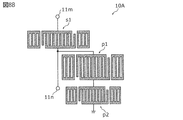
- FIG. 8B is a plan view schematically illustrating the electrode structure of the filter according to the modification of the first embodiment.
- FIG. 9 is a graph showing characteristics of a filter according to a modification of the first embodiment.
- FIG. 10A is a circuit configuration diagram of a filter in application example 1 of the second embodiment.
- FIG. 10B is a graph illustrating filter characteristics in application example 1 of the second embodiment.
- FIG. 11A is a circuit configuration diagram of a filter in application example 2 of the second embodiment.
- FIG. 11B is a graph showing filter characteristics in application example 2 of the second embodiment.
- FIG. 12A is a circuit configuration diagram of a filter in application example 3 of the second embodiment.
- FIG. 12B is a graph illustrating filter characteristics in application example 3 of the second embodiment.
- FIG. 13A is a circuit configuration diagram of a filter in application example 4 of the second embodiment.
- FIG. 13B is a graph illustrating filter characteristics in application example 4 of the second embodiment.
- FIG. 14A is a circuit configuration diagram of a filter in application example 5 of the second embodiment.
- FIG. 14B is a graph illustrating filter characteristics in Application Example 5 of Embodiment 2.
- FIG. 15 is a configuration diagram of the high-frequency front-end circuit and its peripheral circuits according to the third embodiment.
- FIG. 16 is a configuration diagram of a high-frequency front-end circuit according to a modification of the third embodiment.
- FIG. 17 is a plan view schematically showing an electrode structure of a filter according to another embodiment.
- pass band low band end means “the lowest frequency in the pass band”.
- Passband high band end means “the highest frequency in the passband”.
- pass band lower band side means “outside the pass band and lower frequency side than the pass band”.
- passband high band side means “outside of the pass band and higher in frequency than the pass band”.
- FIG. 1A is a circuit configuration diagram of a filter 10 according to the first embodiment.
- the filter 10 is a high-frequency filter circuit that is disposed, for example, in a front end portion of a multi-mode / multi-band mobile phone.
- the filter 10 is a band-pass filter that is built in a multi-band compatible mobile phone that complies with a communication standard such as LTE (Long Term Evolution) and filters high-frequency signals in a predetermined band.
- the filter 10 is an elastic wave filter device that filters high-frequency signals using an elastic wave resonator.
- the filter 10 includes a series arm resonator s1 and parallel arm resonators p1 and p2.
- the series arm resonator s1 is connected between the input / output terminal 11m (first input / output terminal) and the input / output terminal 11n (second input / output terminal). That is, the series arm resonator s1 is a series arm resonance circuit provided on a path connecting the input / output terminal 11m and the input / output terminal 11n. Note that the path is not limited to the series arm resonator s1, but may be provided with a series arm resonance circuit including one or more elastic wave resonators. In the present embodiment, the series arm resonance circuit is configured by one elastic wave resonator, but may be configured by a plurality of elastic wave resonators.
- the series arm resonance circuit including a plurality of elastic wave resonators includes, for example, a longitudinally coupled resonator including a plurality of elastic wave resonators, or a plurality of a plurality of elastic wave resonators divided in series or in parallel.
- a split resonator is included.
- a longitudinally coupled resonator as the series arm resonance circuit, it becomes possible to adapt to required filter characteristics such as enhancement of attenuation.
- the parallel arm resonator p1 is a first parallel arm resonator connected to a node (node x1 in FIG. 1A) and a ground (reference terminal) on a path connecting the input / output terminal 11m and the input / output terminal 11n. . That is, the parallel arm resonator p1 is a resonator provided in a parallel arm resonance circuit that connects the node x1 on the path and the ground.
- the parallel arm resonator p2 is a second parallel arm resonator connected to a node (node x1 in FIG. 1A) and a ground (reference terminal) on the path connecting the input / output terminal 11m and the input / output terminal 11n. . That is, the parallel arm resonator p2 is a resonator provided in a parallel arm resonance circuit that connects the node x1 on the path and the ground.
- parallel arm resonators p1 and p2 are connected between the same node x1 on the series arm and the ground.
- the parallel arm resonators p1 and p2 are connected in parallel and connected between the node x1 and the ground.
- the “same node” includes not only one point on the transmission line but also two different points on the transmission line located without a resonator or an impedance element.
- the node x1 is on the input / output terminal 11n side of the series arm resonator s1, but may be on the input / output terminal 11m side of the series arm resonator s1.
- the parallel arm resonators p1 and p2 constitute a parallel arm resonance circuit connected between the node x1 on the path connecting the input / output terminal 11m and the input / output terminal 11n and the ground. That is, the parallel arm resonance circuit is provided in one path connecting the path and the ground. Therefore, the series arm resonance circuit (series arm resonator s1 in the present embodiment) has a ladder-type filter structure (in this embodiment, the parallel arm resonance circuit (parallel arm resonators p1 and p2 in the present embodiment)). 1-stage ladder type filter structure).
- the parallel arm resonance circuit constituted by the parallel arm resonators p1 and p2 forms the passband of the filter 10 together with the series arm resonator s1.
- FIG. 1B is a plan view schematically showing the electrode structure of the filter 10 according to the first embodiment.
- each resonator (series arm resonator s1, parallel arm resonator p1 and p2) constituting the filter 10 is an elastic wave resonator using an elastic wave.
- the filter 10 can be constituted by an IDT (InterDigital Transducer) electrode formed on a piezoelectric substrate, so that a small and low-profile filter circuit having a pass characteristic with improved steepness can be realized.
- the substrate having piezoelectricity is a substrate having piezoelectricity at least on the surface.
- the substrate may include a piezoelectric thin film on the surface, a film having a different sound velocity from the piezoelectric thin film, and a laminated body such as a support substrate.
- the substrate includes, for example, a laminate including a high sound speed support substrate and a piezoelectric thin film formed on the high sound speed support substrate, a high sound speed support substrate, and a low sound speed film formed on the high sound speed support substrate.
- a laminate including a piezoelectric thin film formed on the film may be used. Note that the substrate may have piezoelectricity throughout the substrate.
- Each resonator has an IDT electrode that excites an elastic wave, and a pair of reflectors arranged so as to sandwich the IDT electrode from both sides in the elastic wave propagation direction.
- the series arm resonator s1 includes an IDT electrode 111 and a pair of reflectors 112.
- the parallel arm resonator p ⁇ b> 1 includes an IDT electrode 121 and a pair of reflectors 122.
- the parallel arm resonator p ⁇ b> 2 includes an IDT electrode 131 and a pair of reflectors 132.
- the resonance frequency (frequency of a resonance point described later) in the parallel arm resonator p2 (second parallel arm resonator) is higher than the resonance frequency in the parallel arm resonator p1 (first parallel arm resonator).
- the anti-resonance frequency (frequency of an anti-resonance point described later) in the parallel arm resonator p2 is higher than the anti-resonance frequency in the parallel arm resonator p1.
- the IDT electrode 131 in the parallel arm resonator p2 has an aspect ratio L / N that is a ratio of the crossing width L of the plurality of electrode fingers to the number N of the plurality of electrode fingers than the IDT electrode 121 in the parallel arm resonator p1. Is small. Furthermore, in the present embodiment, the IDT electrode 111 in the series arm resonator s1 (series arm resonance circuit) has a smaller aspect ratio L / N than the IDT electrode 121 in the parallel arm resonator p1, and the parallel arm resonator. The aspect ratio L / N is larger than the IDT electrode 131 at p2.
- the ratio L / N satisfies L p1 / N p1> L s1 / N s1> L p2 / N p2.
- the logarithms of the IDT electrodes (IDT electrode 111, IDT electrode 121, and IDT electrode 131) of each resonator are shown to be equal, but in an actual design, these logarithms are rarely equal. . That is, design parameters such as the number of IDT electrodes and the crossing width of each resonator can be appropriately determined according to the specifications required for each resonator.
- each resonator constituting the filter 10 will be described in more detail by paying attention to an arbitrary resonator. Since the other resonators have substantially the same structure as the arbitrary resonator, detailed description thereof is omitted.
- FIG. 2 is an example of a diagram schematically showing the structure of the resonator in the present embodiment, where (a) is a plan view and (b) is a cross-sectional view of (a).
- the resonator shown in FIG. 2 is for explaining a typical structure of each resonator constituting the filter 10. For this reason, the number and length of electrode fingers constituting the IDT electrode of each resonator of the filter 10 are not limited to the number and length of electrode fingers of the IDT electrode shown in FIG.
- illustration is abbreviate
- the resonator includes an IDT electrode 101, a piezoelectric substrate 102 on which the IDT electrode 101 is formed, and a protective layer 103 that covers the IDT electrode 101.
- IDT electrode 101 As shown in FIGS. 2A and 2B, the resonator includes an IDT electrode 101, a piezoelectric substrate 102 on which the IDT electrode 101 is formed, and a protective layer 103 that covers the IDT electrode 101.
- protective layer 103 that covers the IDT electrode 101.
- the comb-tooth electrode 101a includes a plurality of electrode fingers 110a that are parallel to each other and a bus bar electrode 111a that connects the plurality of electrode fingers 110a.
- the comb-tooth electrode 101b includes a plurality of electrode fingers 110b that are parallel to each other and a bus bar electrode 111b that connects the plurality of electrode fingers 110b.
- the plurality of electrode fingers 110a and 110b are formed along a direction orthogonal to the propagation direction.
- each of the comb electrodes 101a and 101b may be referred to as an IDT electrode alone. However, in the following description, for the sake of convenience, it is assumed that one IDT electrode 101 is constituted by a pair of comb-tooth electrodes 101a and 101b.
- the IDT electrode 101 composed of the plurality of electrode fingers 110a and 110b and the bus bar electrodes 111a and 111b has a laminated structure of an adhesion layer 101g and a main electrode layer 101h as shown in FIG. It has become.
- the adhesion layer 101g is a layer for improving adhesion between the piezoelectric substrate 102 and the main electrode layer 101h, and Ti is used as a material, for example.
- the film thickness of the adhesion layer 101g is, for example, 12 nm.
- the main electrode layer 101h is made of, for example, Al containing 1% Cu.
- the film thickness of the main electrode layer 101h is, for example, 162 nm.
- the piezoelectric substrate 102 is a substrate on which the IDT electrode 101 is formed, and is made of, for example, LiTaO 3 piezoelectric single crystal, LiNbO 3 piezoelectric single crystal, KNbO 3 piezoelectric single crystal, crystal, or piezoelectric ceramic.
- the protective layer 103 is formed to cover the comb electrodes 101a and 101b.
- the protective layer 103 is a layer for the purpose of protecting the main electrode layer 101h from the external environment, adjusting frequency temperature characteristics, and improving moisture resistance, for example, a film mainly composed of silicon dioxide. .
- a resonator configured in this way has a “singular point” where the impedance is minimal (ideally the point where the impedance is 0) and a singular point where ideal impedance is the maximum (ideally It has an “anti-resonance point” that is an infinite point.
- each resonator which the filter 10 has is not limited to the structure described in FIG.
- the IDT electrode 101 may not be a stacked structure of metal films but may be a single layer of metal films.
- the materials constituting the adhesion layer 101g, the main electrode layer 101h, and the protective layer 103 are not limited to the materials described above.
- the IDT electrode 101 may be made of, for example, a metal or an alloy such as Ti, Al, Cu, Pt, Au, Ag, or Pd, and is made of a plurality of laminates made of the above metals or alloys. May be.
- the protective layer 103 may not be formed.
- the wavelength of the excited elastic wave is defined by the design parameters of the IDT electrode 101 and the like.
- design parameters of the IDT electrode 101 that is, design parameters of the comb electrode 101a and the comb electrode 101b will be described.
- the wavelength of the elastic wave is defined by the repetition period ⁇ of the plurality of electrode fingers 110a or 110b constituting the comb electrodes 101a and 101b shown in FIG.
- the electrode pitch (electrode period) is 1 ⁇ 2 of the repetition period ⁇
- the line width of the electrode fingers 110a and 110b constituting the comb electrodes 101a and 101b is W
- the adjacent electrode fingers 110a and electrodes When the space width between the finger 110b is S, it is defined by (W + S).
- the crossing width L of the IDT electrode 101 is obtained by viewing the electrode finger 110a of the comb electrode 101a and the electrode finger 110b of the comb electrode 101b from the propagation direction of the elastic wave.
- the electrode duty (hereinafter referred to as duty ratio) is the line width occupation ratio of the plurality of electrode fingers 110a and 110b, and the ratio of the line width to the sum of the line width and the space width of the plurality of electrode fingers 110a and 110b. And is defined by W / (W + S).
- the film thickness of the IDT electrode 101 is the thickness h of the plurality of electrode fingers 110a and 110b.
- a singular point where the impedance is minimized (ideally a point where the impedance is 0) is also referred to as a “resonance point” for convenience, not only for a single resonator but also for a circuit including a plurality of resonators.
- the frequency is called “resonance frequency”.
- a singular point where the impedance is maximum (ideally a point where the impedance is infinite) is called an “anti-resonance point”, and its frequency is called an “anti-resonance frequency”.
- FIG. 3 is a graph showing the characteristics of the filter 10 according to the first embodiment. Specifically, (a) of the figure is a graph showing impedance characteristics of the parallel arm resonators p1 and p2 and the series arm resonator s1.
- FIG. 4B is a graph showing the combined impedance characteristics (synthetic characteristics) of the parallel arm resonators p1 and p2 and the impedance characteristics of the series arm resonator s1.
- FIG. 4C is a graph showing the filter characteristics of the filter 10.
- the parallel arm resonator p1, the parallel arm resonator p2, and the series arm resonator s1 have the following impedance characteristics. Specifically, for the parallel arm resonator p1, the parallel arm resonator p2, and the series arm resonator s1, in this order, assuming that the resonance frequencies are frp1, frp2, frs1, and the antiresonance frequencies are fap1, fap2, and fas1, In this form, frp1 ⁇ frs1 ⁇ frp2 and fap1 ⁇ fas1 ⁇ fap2 are satisfied.
- the combined characteristics of the two parallel arm resonators (“parallel arm resonators p1 and p2) (“the combined characteristics of the parallel arms (p1 + p2)” in the figure) are the parallel arm resonators. It becomes minimum at the resonance frequency frp2 of p2 and the resonance frequency frp1 of the parallel arm resonator p1. Further, the combined characteristic becomes maximum at a frequency between the two resonance frequencies frp2 and frp1 and a frequency between the two antiresonance frequencies fap2 and fap1.
- the low-frequency side anti-resonance frequency of the two anti-resonance frequencies of the parallel arm resonance circuit and the resonance frequency frs1 of the series arm resonator s1 are placed close to each other. Configure the bandwidth.
- an attenuation band having the attenuation pole as the resonance frequency frp1 of the parallel arm resonator p1 is formed on the low pass band side.
- an attenuation band having an attenuation pole with the resonance frequency frp2 of the parallel arm resonator p2 and the antiresonance frequency fas1 of the series arm resonator s1 is formed on the high side of the pass band.
- the low-frequency side anti-resonance frequency (Fa1 in FIG. 3) and the high-frequency side resonance frequency (Fr2 in FIG. 3) of the combined impedance characteristics of the parallel arm resonator p1 and the parallel arm resonator p2 are:
- An attenuation slope on the high band side of the pass band of the filter 10 is defined.
- the sharpness of the attenuation slope on the high side of the pass band is the difference between the low side anti-resonance frequency (Fa1 in FIG. 3) and the high side resonance frequency (Fr2 in FIG. 3) in the above synthetic impedance characteristic. It is influenced by the sharpness of the slope between.
- the Q of the anti-resonance frequency of the parallel arm resonator p1 (Fap1 in FIG. 3) and the Q of the resonance frequency of the parallel arm resonator p2 (Frp2 in FIG. 3) Affects.
- the anti-resonance frequency Q of the parallel arm resonator p1 is higher, in the combined impedance characteristic of the parallel arm resonance circuit (in this embodiment, the parallel connection circuit of the parallel arm resonators p1 and p2), Q of the side anti-resonance frequency (Fa1 in FIG. 3) becomes high.
- the higher the resonance frequency Q of the parallel arm resonator p2 the higher the Q of the resonance frequency (Fr2 in FIG.
- the sharpness of the slope between the anti-resonance frequency on the low frequency side and the resonance frequency on the high frequency side is improved.
- the sharpness on the high side of the passband can be improved.
- the higher the resonance frequency Q of the parallel arm resonator p2 the higher the Q of the attenuation pole (PoleH in FIG. 3) on the higher passband side (that is, the deeper the attenuation pole), and the parallel arm resonator p1.
- the anti-resonance frequency Q is higher, the loss in the passband (PB in FIG. 3) is suppressed. For this reason, the sharpness at the high side of the pass band can be improved.
- the combined impedance characteristic of the parallel arm resonance circuit is a characteristic in which the capacitance component of the parallel arm resonator p2 is combined with the characteristic of the parallel arm resonator p1 in the vicinity of the anti-resonance frequency on the low frequency side. Therefore, in addition to increasing the antiresonance frequency Q of the parallel arm resonator p1, in addition to increasing the Q of the capacitance component of the parallel arm resonator p2, that is, by reducing the series resistance of the parallel arm resonator p2, Loss in the passband of the filter 10 can be suppressed.
- the parallel arm resonator p2 is configured by the IDT electrode 131 having a smaller aspect ratio than the IDT electrode 121 of the parallel arm resonator p1.
- the filter 10 can reduce the loss in the pass band and improve the sharpness on the high side of the pass band.
- the reason why such an effect is achieved will be described including the background to the present invention.
- the following typical example 1 has a frequency band different from that of the present embodiment, but the tendency of the resonance frequency and anti-resonance frequency Q to change depending on the aspect ratio of the IDT electrode is the frequency of the present embodiment. The same applies to the band. Further, in the following typical example 1, since the logarithm is varied in a state where the impedance of the resonator is constant (that is, the capacitance is constant), the crossing width is adjusted depending on the logarithm.
- FIG. 4 is a graph showing impedance characteristics when the aspect ratio is changed in the resonator of the first representative example.
- (a) represents the overall impedance characteristic
- (b) is a graph showing an enlarged impedance characteristic near the resonance frequency of (a)
- (c) is an anti-resonance frequency of (a). It is a graph which expands and represents the impedance characteristic of vicinity.
- the aspect ratio crossover width / logarithm
- the aspect ratio crossover width / logarithm
- Table 1 shows details of the design parameters of the resonator at this time.
- Zmin. Is the impedance value of the resonance frequency, that is, the minimum value of the impedance.
- Zmax. Is the impedance value of the antiresonance frequency, that is, the maximum value of the impedance.
- film thickness h is the same for all typical examples.
- FIG. 5 shows the resonance frequency impedance value Zmin. And the anti-resonance frequency impedance value Zmax. It is a graph showing.
- the Zmin. And Zmax. It turns out that all become large. That is, with respect to the resonance frequency, the Q becomes higher as the aspect ratio becomes smaller. On the other hand, with respect to the antiresonance frequency, the Q becomes higher as the aspect ratio becomes larger.
- the filter 10 by reducing the aspect ratio of the IDT electrode 131 in the parallel arm resonator p2 and increasing the aspect ratio of the IDT electrode 121 in the parallel arm resonator p1, the loss in the pass band is reduced and the pass band is increased.
- the sharpness on the high frequency side can be improved.
- the inventor of the present application has found that the ripple in the passband can be suppressed by increasing the logarithm of the IDT electrode 131 in the parallel arm resonator p2.
- the aspect ratio is determined by two factors, the cross width and the logarithm.
- the inventor of the present application increases the aspect ratio of the parallel arm resonator p2 by increasing the logarithm of the two factors. I noticed that it would be preferable to make it smaller. This will be described below based on a specific typical example.
- the following typical example 2 is different in frequency band from the present embodiment, the tendency that the ripple changes depending on the logarithm is the same in the frequency band of the present embodiment.
- the logarithm is oscillated in a state where the impedance of the resonator is constant (that is, the capacitance is constant), so the crossover width depends on the logarithm. Has also been adjusted.
- FIG. 6 is a graph showing characteristics when the logarithm is changed in the resonator of the typical example 2.
- (a) is a graph showing impedance characteristics
- (b) is a graph showing phase characteristics
- (c-1) is an impedance Smith chart showing reflection characteristics
- (c-2) is It is a graph showing reflection characteristics (return loss: reflection loss).
- the aspect ratio crossover width / logarithm
- the aspect ratio crossover width / logarithm
- Table 2 shows details of the design parameters of the resonator at this time.
- surface is abbreviate
- IDT wavelength (lambda) and film thickness h are the same about all the typical examples.
- the frequency band lower than the resonance frequency of the parallel arm resonator p2 is located in the pass band of the filter 10 as shown in FIG. Therefore, from the viewpoint of suppressing ripples in the passband of the filter 10, it is preferable to reduce the aspect ratio by increasing the logarithm of the IDT electrode 131 in the parallel arm resonator p2.
- the present inventor has found that the ripple can be suppressed by increasing the logarithm as a result of intensive studies.
- the number of IDT electrodes 131 is preferably larger than the number of IDT electrodes 121.
- the parallel arm resonator p2 is preferably configured by the IDT electrode 131 having a smaller aspect ratio due to a larger number of logarithms than the parallel arm resonator p1. According to such a configuration, it is possible to reduce the loss in the pass band and improve the sharpness on the high pass band side while suppressing the ripple in the pass band.
- the above ripple is particularly conspicuous when a reflector is provided in the propagation direction of the elastic wave with respect to the IDT electrode.
- the resonator having the reflector is used as the parallel arm resonator p2
- grating refers to a periodic repeating structure formed by a plurality of electrode fingers constituting a reflector. Therefore, by increasing the number of IDT electrodes in the parallel arm resonator p2 having a reflector, it is possible to further reduce the loss while suppressing the ripple in the passband.
- the filter of the example has the configuration of the filter 10 according to the above-described embodiment.
- the filter of the comparative example has substantially the same configuration as the filter of the embodiment, but the parallel arm resonator p1 and the parallel arm resonator p2 are configured by IDT electrodes having the same aspect ratio (cross width / logarithm). Is different.
- Table 3 shows the design parameters (aspect ratio) of the filters of Examples and Comparative Examples.
- the series arm resonator s1 of the example is composed of IDT electrodes having the same aspect ratio as compared to the series arm resonator s1 of the comparative example.
- the parallel arm resonator p1 of the example is configured by an IDT electrode having a larger aspect ratio than the parallel arm resonator p1 of the comparative example. That is, in the embodiment, the parallel arm resonator p1 is configured by an IDT electrode having a larger aspect ratio than the parallel arm resonator p2. In the embodiment, the parallel arm resonator p1 is configured by an IDT electrode having a larger aspect ratio than the series arm resonator s1.
- the parallel arm resonator p2 of the example is configured by an IDT electrode having a smaller aspect ratio than the parallel arm resonator p2 of the comparative example. That is, in the embodiment, the parallel arm resonator p2 is configured by an IDT electrode having a smaller aspect ratio than the parallel arm resonator p1. In the embodiment, the parallel arm resonator p2 is configured by an IDT electrode having a smaller aspect ratio than the series arm resonator s1.
- FIG. 7 is a graph showing the filter characteristics of the filters of the example and the comparative example.
- the loss in the passband is suppressed in the example compared to the comparative example. That is, in the embodiment, the loss in the passband is reduced as compared with the comparative example.
- the parallel arm resonator p2 (second parallel arm resonator) is the parallel arm resonator p1 (first parallel arm resonance).
- the IDT electrode 131 has a higher frequency for exciting the elastic wave and a smaller aspect ratio than the child.
- the present inventor has found the following as a result of intensive studies. That is, regarding the impedance characteristics of a single resonator, the resonance frequency Q increases as the aspect ratio of the IDT electrode decreases, and conversely, the antiresonance frequency Q increases as the aspect ratio of the IDT electrode increases.
- the parallel arm resonator p2 is configured by the IDT electrode 131 having a smaller aspect ratio than the parallel arm resonator p1.
- the electrode finger resistance decreases as the cross width L (see FIG. 2) decreases. That is, by reducing the crossover width, it is possible to reduce the series resistance, which is a factor that degrades the resonance frequency Q in the resonator. Therefore, reducing the overlap width L p2 of the IDT electrode 131 in the parallel arm resonators p2, i.e. by reducing the aspect ratio, possible to further improve the sharpness of a further low-loss reduction and the high-frequency side of the passband of the passband Can do.
- the series arm resonator s1 is configured by the IDT electrode 111 having a smaller aspect ratio than the parallel arm resonator p1.
- the passband of the filter 10 includes the resonance frequency of the series arm resonator s1 and the anti-resonance frequency on the low band side of the parallel arm resonance circuit (in this embodiment, the parallel connection circuit of the parallel arm resonators p1 and p2). Formed with.
- the resonance frequency Q increases as the aspect ratio of the IDT electrode decreases, and conversely, the antiresonance frequency Q increases as the aspect ratio of the IDT electrode increases. For this reason, by further reducing the aspect ratio of the IDT electrode 111 in the series arm resonator s1, it is possible to further reduce the loss in the passband.
- the series arm resonator s1 is configured by the IDT electrode 111 having a larger aspect ratio than the parallel arm resonator p2.
- the parallel arm resonator p2 forms an attenuation pole whose resonance frequency is on the high side of the pass band, but the anti-resonance frequency does not contribute much to the formation of the filter characteristics.
- the resonance characteristic is hardly affected. For this reason, there is no particular problem in reducing the cross width L p2 of the parallel arm resonator p2 from the viewpoint of filter characteristics.
- the cross width L s1 of the series arm resonator s1 becomes too small.
- the influence of the diffraction loss due to can be suppressed. For this reason, it is possible to reduce the loss in the pass band and improve the sharpness on the high pass band side while suppressing the deterioration of the filter characteristics due to the diffraction loss.
- the parallel arm resonators p1 and p2 are connected in parallel to each other and connected to the same node x1 (node) of the series arm.
- the parallel arm resonators p1 and p2 may be connected in series with each other and connected to the same node x1 (node) of the series arm. Therefore, such a filter will be described as a filter according to a modification of the first embodiment.
- FIG. 8A is a circuit configuration diagram of a filter 10A according to a modification of the first embodiment.
- FIG. 8B is a plan view schematically showing an electrode structure of filter 10A according to the modification of Embodiment 1.
- the filter 10A shown in these drawings includes an input / output terminal 11m (first input / output terminal) and parallel arm resonators p1 and p2 connected in series. The difference is that it is connected between the same node x1 in the path connecting the input / output terminal 11n (second input / output terminal) and the ground.
- the parallel arm resonator p1 has one terminal connected to the node x1 and the other terminal connected to one terminal of the parallel arm resonator p2.
- the parallel arm resonator p2 has one terminal connected to the other terminal of the parallel arm resonator p1, and the other terminal connected to the ground.
- the connection order of the parallel arm resonators p1 and p2 is not limited to this, and the connection order may be reversed.
- FIG. 9 is a graph showing characteristics of the filter 10A according to the modification of the first embodiment.
- the Q of the antiresonance frequency (Fap1 in FIG. 9) of the parallel arm resonator p1 and the parallel arm are similar to the characteristics of the filter 10 according to the first embodiment.
- the Q of the resonance frequency of the resonator p2 affects the sharpness on the high side of the passband. The specific mechanism related to this is the same as that in the first embodiment, and a detailed description thereof will be omitted.
- the combined impedance characteristics of the parallel arm circuit are combined with the characteristics of the parallel arm resonator p1 and the capacitance component of the parallel arm resonator p2 in the vicinity of the anti-resonance frequency on the low frequency side. Characteristics. Therefore, in addition to increasing the antiresonance frequency Q of the parallel arm resonator p1, in addition to increasing the Q of the capacitance component of the parallel arm resonator p2, that is, by reducing the series resistance of the parallel arm resonator p2, Loss in the passband of the filter 10A can be suppressed.
- the parallel arm resonator p2 is configured by the IDT electrode having a smaller aspect ratio than the parallel arm resonator p1, so that, similarly to the first embodiment, It is possible to reduce the loss on the high side of the passband and improve the sharpness.
- Embodiment 2 The configuration of the filter (elastic wave filter device) according to the first embodiment and its modification can be applied to a tunable filter whose passband can be varied. Therefore, as a filter according to Embodiment 2, such a tunable filter will be described using application examples 1 to 5.
- application examples 1 to 4 are application examples of the filter 10 according to the first embodiment to the tunable filter
- application example 5 is an example of the filter 10A according to the modification of the first embodiment. This is an application example to a tunable filter.
- Each of the tunable filters of Application Examples 1 to 5 described below includes a switch element connected in series or in parallel to the parallel arm resonator p1 or the parallel arm resonator p2, and the switch element is turned on (ON).
- the pass band is switched according to non-conduction (off).
- the switch element is turned on and off in accordance with a control signal from a control unit such as an RF signal processing circuit (RFIC: Radio Frequency Integrated Circuit).
- RFIC Radio Frequency Integrated Circuit
- FIG. 10A is a circuit configuration diagram of a filter 20A in application example 1 of the second embodiment.
- the filter 20A shown in the same figure further includes at least one of the parallel arm resonators p1 and p2 (first parallel arm resonator and second parallel arm resonator) (this application example). Then, it has a pair of capacitor C and switch SW connected in series to the parallel arm resonator p2) and connected in parallel to each other. Accordingly, the filter 20A can switch between the first passband and the second passband according to the conduction and non-conduction of the switch SW. Specifically, in this application example, the pair of capacitors C and switches SW connected in parallel to each other are connected in series only to the parallel arm resonator p2 of the parallel arm resonators p1 and p2.
- the filter 20A further includes an impedance circuit that is a circuit in which a pair of capacitors C and a switch SW are connected in parallel. At least one of the parallel arm resonators p1 and p2 is connected in series with the impedance circuit.
- the parallel arm resonator p2 (second parallel arm resonator) is connected in series with the impedance circuit, and the parallel arm resonator p1 (first parallel arm resonator) is connected in parallel.
- the arm resonator p2 and the impedance circuit are connected in parallel to a circuit connected in series.
- a circuit in which the capacitor C and the switch SW are connected in parallel is connected in series to the parallel arm resonator p2 between the node x1 and the ground, and specifically, the ground and the parallel arm resonator p2 are connected. Are connected in series.
- the capacitor C and the switch SW may be connected between the node x1 and the parallel arm resonator p2.
- the capacitor C is an impedance element connected in series to the parallel arm resonator p2.
- the frequency variable width of the passband of the filter 20A depends on the constant of the capacitor C. For example, the smaller the constant of the capacitor C, the wider the frequency variable width. For this reason, the constant of the capacitor C can be appropriately determined according to the frequency specification required for the filter 20A.
- the capacitor C may be a variable capacitor such as a variable gap and a DTC (Digital Tunable Capacitor). As a result, the frequency variable width can be finely adjusted.
- the switch SW is, for example, a SPST (Single Pole Single Throw) type switch element in which one terminal is connected to a connection node between the parallel arm resonator p2 and the capacitor C and the other terminal is connected to the ground.
- the switch SW switches between conduction (on) and non-conduction (off) in accordance with a control signal from a control unit (not shown), thereby bringing the connection node and ground into conduction or non-conduction.
- the switch SW may be a FET (Field Effect Transistor) switch made of GaAs or CMOS (Complementary Metal Oxide Semiconductor), or a diode switch.
- FET Field Effect Transistor
- CMOS Complementary Metal Oxide Semiconductor
- the switch SW can be constituted by one FET switch or a diode switch, the filter 20A can be reduced in size.
- the parallel arm resonators p1 and p2, the capacitor C, and the switch SW constitute a parallel arm resonance circuit connected between the node x1 on the path connecting the input / output terminal 11m and the input / output terminal 11n and the ground. . That is, the parallel arm resonance circuit is provided in one path connecting the path and the ground. Therefore, the filter 20A has a one-stage ladder-type filter structure including the series arm resonator s1 and the parallel arm resonance circuit.
- both the resonance frequency and the anti-resonance frequency are switched to the low band side or both to the high band side according to switching of the switch SW on (conducting) and off (non-conducting). This will be described later together with the characteristics of the filter 20A.
- FIG. 10B is a graph showing characteristics of the filter 20A in the application example 1 of the second embodiment.
- (a) of the figure is a graph showing impedance characteristics of a single resonator (parallel arm resonators p1 and p2 and series arm resonator s1 respectively).
- (B) of the figure shows the combined impedance of the parallel arm resonance circuit when the switch SW is on and off (in this application example, a circuit composed of the parallel arm resonators p1 and p2 and the capacitor C and the switch SW). It is a graph which compares and represents a characteristic (composite characteristic). In the figure, impedance characteristics of the series arm resonator s1 are also shown.
- (C) of the same figure is a graph showing a comparison of filter characteristics when the switch SW is on and when it is off.
- the passband of the filter 20A is defined by the lower resonance frequency frs1 of the parallel arm resonance circuit and the resonance frequency frs1 of the series arm resonator s1.
- the pole (attenuation pole) on the low side of the passband is defined by the resonance frequency frp1 of the parallel arm resonator p1, and the passband height is determined by the resonance frequency frp2 of the parallel arm resonator p2 and the antiresonance frequency fas1 of the series arm resonator s1. It has a first passing characteristic in which a pole on the band side (attenuation pole) is defined.
- the impedance characteristic of the parallel arm resonance circuit is affected by the capacitor C.
- the combined characteristic of the two parallel arm resonators (parallel arm resonators p1 and p2) and the capacitor C is the impedance characteristic of the parallel arm resonance circuit.
- the anti-resonance frequency on the low band side and the resonance frequency on the high band side of the parallel arm resonance circuit define an attenuation slope on the high band side of the passband of the filter 20A. Therefore, as shown in (c) of the figure, when the switch SW is switched from on to off, the pass characteristic of the filter 20A maintains the steepness of the attenuation slope on the high side of the passband from the first characteristic. Switching to the second characteristic shifted to the high frequency side. In other words, the filter 20A changes the frequency of the attenuation pole on the passband high band side in accordance with switching between the conduction and non-conduction of the switch SW and suppresses an increase in insertion loss at the high end of the passband. The characteristic and the second characteristic can be switched.
- the parallel arm resonator p2 is configured by the IDT electrode having a smaller aspect ratio than the parallel arm resonator p1, so that each of the first pass characteristic and the second pass characteristic is obtained.
- the filter 20A constitutes a tunable filter that can reduce loss and improve sharpness on the high side of the passband.
- the impedance element is not limited to a capacitor, and may be an inductor, for example.
- an inductor is used as the impedance element, the shift direction of the attenuation slope when the switch SW is turned on and off is different from that in the above configuration. Specifically, in the second pass characteristic when the switch SW is off, the attenuation slope is shifted to the low frequency side compared to the first pass characteristic when the switch SW is on.
- the frequency variable width of the passband of the filter 20A depends on the constant of the inductor. For example, the larger the inductor constant, the wider the frequency variable width. For this reason, the constant of the inductor can be appropriately determined according to the frequency specification required for the filter 20A.
- the inductor may be a variable inductor using MEMS (Micro Electro Mechanical Systems). As a result, the frequency variable width can be finely adjusted.
- FIG. 11A is a circuit configuration diagram of a filter 20B in application example 2 of the second embodiment.
- the filter 20B shown in the figure includes a pair of capacitors C and a switch SW connected in parallel with each other, and only the parallel arm resonator p1 of the parallel arm resonators p1 and p2 is connected in series. The connection is different.
- the parallel arm resonator p2 is connected in series to the impedance circuit that is a circuit in which the pair of capacitors C and the switch SW are connected in parallel.
- the parallel arm resonator p1 first parallel arm resonator
- the parallel arm resonator p2 second parallel arm resonator
- the child p1 and the impedance circuit are connected in parallel to the circuit connected in series.
- FIG. 11B is a graph showing characteristics of the filter 20B in the application example 2 of the second embodiment. Specifically, (a) and (b) in the figure are graphs showing the impedance characteristics of a single resonator and the combined impedance characteristics of the parallel arm resonance circuit, as in (a) and (b) of FIG. 10B. is there. (C) of the same figure is a graph showing a comparison of filter characteristics when the switch SW is on and when it is off.
- the anti-resonance frequency on the low frequency side and the resonance frequency on the low frequency side of the parallel arm resonance circuit define an attenuation slope on the low frequency side of the pass band of the filter 20B. Therefore, as shown in (c) of the figure, when the switch SW is switched from ON to OFF, the pass characteristic of the filter 20B maintains the steepness of the attenuation slope on the low pass band side from the first pass characteristic. While switching to the second pass characteristic shifted to the high frequency side. In other words, the filter 20B can switch the attenuation pole on the low side of the passband according to switching between conduction and non-conduction of the switch SW, and can suppress an increase in insertion loss at the low end of the passband.
- the parallel arm resonator p2 is composed of IDT electrodes having a smaller aspect ratio than the parallel arm resonator p1, so that each of the first pass characteristic and the second pass characteristic is obtained.
- the filter 20B constitutes a tunable filter that can reduce loss and improve sharpness on the high side of the passband.
- FIG. 12A is a circuit configuration diagram of a filter 20C in application example 3 of the second embodiment.
- the filter 20C shown in the figure shifts both the attenuation slopes on the high side of the passband and the low side of the passband.
- the filter 20C includes a pair of capacitors C (impedance elements) included in the filter 20B illustrated in FIG. 11A and a capacitor C1 and a switch SW1 corresponding to the switch SW.
- the filter 20C includes a pair of capacitors C (impedance elements) included in the filter 20A illustrated in FIG. 10A and a capacitor C2 and a switch SW2 corresponding to the switch SW.
- the filters 20A and 20B have one impedance circuit that is a circuit in which a pair of capacitors C and a switch SW are connected in parallel.
- the filter 20C has two impedance circuits.
- the parallel arm resonator p1 first parallel arm resonator
- the parallel arm resonator p2 second parallel arm resonator
- the circuit in which the parallel arm resonator p1 and one impedance circuit are connected in series and the circuit in which the parallel arm resonator p2 and the other impedance circuit are connected in series are connected in parallel.
- FIG. 12B is a graph showing characteristics of the filter 20C in the application example 3 of the second embodiment. Specifically, (a) and (b) in the same figure are similar to (a) and (b) in FIG. 10B, and impedance characteristics of a single resonator and a parallel arm resonance circuit (in this application example, parallel arm resonance). It is a graph showing the synthetic
- FIG. 6C is a graph showing the comparison of filter characteristics when both the switches SW1 and SW2 are on or off.
- the pass characteristic of the filter 20C is changed from the first pass characteristic to the pass band high band side and the pass band low band side. Is switched to the second passing characteristic shifted to the high frequency side while maintaining the steepness.
- the filter 20C can switch the frequencies of the attenuation poles on the high side of the passband and the low side of the passband according to the switching of the conduction and non-conduction of the switches SW1 and WS2, and at the high end of the passband.
- an increase in insertion loss at the low end of the passband can be suppressed. For this reason, for example, the filter 20C can switch the center frequency while maintaining the bandwidth.
- the parallel arm resonator p ⁇ b> 2 is composed of IDT electrodes having a smaller aspect ratio than the parallel arm resonator p ⁇ b> 1, so that each of the first pass characteristic and the second pass characteristic is obtained.
- the filter 20 ⁇ / b> C constitutes a tunable filter that can reduce loss and improve sharpness on the high side of the passband.
- the switches SW1 and SW2 may not be switched on and off, or may be switched individually. However, when both of the switches SW1 and SW2 are switched on and off, the number of control lines for controlling the switches SW1 and SW2 can be reduced, so that the configuration of the filter 20C can be simplified.
- the high band end of the pass band can be varied according to the on / off state of the switch SW2 connected in series to the parallel arm resonator p2.
- the low band end of the pass band can be varied according to the on / off state of the switch SW1 connected in series to the parallel arm resonator p1.
- both the switches SW1 and SW2 on or off, it is possible to shift both the low band end and high band end of the pass band to the low band side or the high band side. That is, the center frequency of the pass band can be shifted to the low frequency side or the high frequency side.
- both the low band end and high band end of the pass band are shifted so that these frequency differences are widened or narrowed. be able to. That is, the pass band width can be varied while making the center frequency of the pass band substantially constant.
- the other when one of the switches SW1 and SW2 is turned on or off, the other is turned on and off, so that one of the low band end and the high band end of the pass band is fixed and the other is connected to the low band side or the high band. Can be shifted to the side. That is, the low band end or high band end of the pass band can be varied.
- FIG. 13A is a circuit configuration diagram of a filter 20D in application example 4 of the second embodiment.
- the filter 20D shown in FIG. 10 has a pair of capacitors C and a switch SW connected in parallel to each other, and the parallel arm resonator p1 and the parallel arm resonator p2 are connected in parallel. The difference is that they are connected in series to the circuit.
- the parallel arm resonator p1 first parallel arm resonator
- the parallel arm resonator p2 second parallel arm resonator
- An impedance circuit which is a circuit in which a pair of capacitors C and a switch SW are connected in parallel, is connected in series to a circuit in which the parallel arm resonator p1 and the parallel arm resonator p2 are connected in parallel.
- FIG. 13B is a graph showing characteristics of the filter 20D in the application example 4 of the second embodiment. Specifically, (a) and (b) in the figure are graphs showing the impedance characteristics of a single resonator and the combined impedance characteristics of the parallel arm resonance circuit, as in (a) and (b) of FIG. 10B. is there. (C) of the same figure is a graph showing a comparison of filter characteristics when the switch SW is on and when it is off.
- the pass characteristic of the filter 20D is such that the poles (attenuation poles) on both sides of the pass band from the first pass characteristic are higher. To the second passage characteristic shifted to.
- the parallel arm resonator p2 is configured by the IDT electrode having a smaller aspect ratio than the parallel arm resonator p1, so that each of the first pass characteristic and the second pass characteristic is obtained.
- the filter 20D constitutes a tunable filter that can reduce loss and improve sharpness on the high side of the passband.
- FIG. 14A is a circuit configuration diagram of a filter 20E according to Application Example 5 of Embodiment 2.
- the filter 20E shown in FIG. 8 further includes one of the parallel arm resonators p1 and p2 (first parallel arm resonator and second parallel arm resonator). Are connected in parallel.
- the other parallel arm resonator of the parallel arm resonators p1 and p2 is connected in series to a circuit in which the one parallel arm resonator and the switch SW are connected in parallel.
- the switch SW is connected in parallel to the parallel arm resonator p2.
- the switch SW may be connected in parallel to the parallel arm resonator p1 when the influence of the diffraction loss of the parallel arm resonator p2 is allowed according to the required specifications for the filter 20E.
- FIG. 14B is a graph showing characteristics of the filter 20E in the application example 5 of the second embodiment. Specifically, (a) and (b) in the same figure are similar to (a) and (b) in FIG. 10B, and impedance characteristics of a single resonator and a parallel arm resonance circuit (in this application example, parallel arm resonance). It is a graph showing the synthetic
- the impedance characteristic of the parallel arm resonance circuit (the synthesis characteristic of the parallel arms in the figure) is the impedance characteristic of the parallel arm resonator p1 alone.
- the parallel arm resonator p2 is added to the parallel arm resonator p1.
- the impedance characteristic of the parallel arm resonance circuit (the combined characteristic of the parallel arms in the figure) is the parallel arm resonator.
- the pass characteristic of the filter 20E shifts the attenuation pole on the low band side to the high band side and the pass band. Since an attenuation pole is added on the high frequency side (Pole H in the figure), it is possible to obtain attenuation on the high frequency side of the pass band.
- the filter 20E can switch the frequency of the attenuation pole on the low-passband side and switch the number of attenuation poles on the high-passband side in accordance with the on / off switching of the switch SW. it can.
- the parallel arm resonator p2 includes the IDT electrode having a smaller aspect ratio than the parallel arm resonator p1, so that the parallel arm resonator p1 has the parallel arm resonator p2.
- the filter 20E constitutes a tunable filter that can reduce loss and improve sharpness on the high side of the passband.
- FIG. 15 is a configuration diagram of the high-frequency front-end circuit 1 and its peripheral circuits according to the third embodiment.
- a high-frequency front-end circuit 1 an antenna element 2, and an RF signal processing circuit (RFIC) 3 are shown.
- the high-frequency front end circuit 1, the antenna element 2, and the RFIC 3 constitute a communication device 4.
- the antenna element 2, the high-frequency front end circuit 1, and the RFIC 3 are disposed, for example, in a front end portion of a mobile phone that supports multimode / multiband.
- the antenna element 2 is a multiband antenna that transmits and receives a high-frequency signal and is used in conformity with a communication standard such as 3GPP (Third Generation Partnership Project).
- the antenna element 2 may not correspond to, for example, all the bands of the communication device 4, and may correspond to only the bands of the low frequency band group or the high frequency band group.
- the antenna element 2 is not built in the communication device 4 and may be provided separately from the communication device 4.
- the high frequency front end circuit 1 is a circuit that transmits a high frequency signal between the antenna element 2 and the RFIC 3. Specifically, the high-frequency front end circuit 1 transmits the high-frequency transmission signal output from the RFIC 3 to the antenna element 2 via the transmission-side signal path. The high-frequency front end circuit 1 transmits a high-frequency reception signal received by the antenna element 2 to the RFIC 3 via the reception-side signal path.
- the high-frequency front-end circuit 1 includes a duplexer 120, a transmission amplifier circuit 140, and a reception amplifier circuit 160.
- the duplexer 120 is a multiplexer that includes a transmission-side filter 120Tx and a reception-side filter 120Rx, and includes the above-described elastic wave filter device in at least one of them.
- the transmission-side filter 120Tx and the reception-side filter 120Rx have the antenna-side input / output terminals bundled together and connected to the antenna element 2, and the other terminals connected to the transmission amplifier circuit 140 or the reception amplifier circuit 160.
- the transmission amplifier circuit 140 is a power amplifier that amplifies the power of the high-frequency transmission signal output from the RFIC 3.
- the reception amplification circuit 160 is a low noise amplifier that amplifies the power of the high frequency reception signal received by the antenna element 2.
- RFIC 3 is an RF signal processing circuit that processes high-frequency signals transmitted and received by the antenna element 2. Specifically, the RFIC 3 performs signal processing on the high-frequency reception signal input from the antenna element 2 via the reception-side signal path of the high-frequency front-end circuit 1 by down-conversion or the like, and receives the signal generated by the signal processing. The signal is output to a baseband signal processing circuit (not shown). The RFIC 3 also performs signal processing on the transmission signal input from the baseband signal processing circuit by up-conversion or the like, and outputs the high-frequency transmission signal generated by the signal processing to the transmission-side signal path of the high-frequency front-end circuit 1. .
- high-frequency front-end circuit 1 by providing the elastic wave filter device described above, low loss and high selectivity (inhibition of mutual interference with other bands adjacent to the own band) are achieved. Both can be achieved. For this reason, it is particularly useful as the high-frequency front-end circuit 1 applied to the communication device 4 that supports multiband.
- the filter (elastic wave filter device) described in the first and second embodiments and the modifications thereof is a high frequency front corresponding to a system having a larger number of bands used than the high frequency front end circuit 1 according to the third embodiment. It can also be applied to an end circuit. Therefore, in this modification, such a high-frequency front end circuit will be described.
- FIG. 16 is a configuration diagram of a high-frequency front-end circuit 1A according to a modification of the third embodiment.
- the high-frequency front end circuit 1A includes an antenna terminal ANT, transmission terminals Tx1 and Tx2, and reception terminals Rx1 and Rx2, and a switch group 110 including a plurality of switches in order from the antenna terminal ANT side.
- the filter group 120A includes a plurality of filters, transmission-side switches 130A and 130B, reception-side switches 150A, 150B, and 150C, transmission amplification circuits 140A and 140B, and reception amplification circuits 160A and 160B.
- the switch group 110 connects the antenna terminal ANT and a signal path corresponding to a predetermined band according to a control signal from a control unit (not shown), and includes, for example, a plurality of SPST type switches.
- the number of signal paths connected to the antenna terminal ANT is not limited to one, and a plurality of signal paths may be used. That is, the high-frequency front end circuit 1A may support carrier aggregation.
- the filter group 120A includes, for example, a plurality of filters (including a duplexer) having the following band in the pass band.
- the band includes (i) Band 12 transmission band, (ii) Band 13 transmission band, (iii) Band 14 transmission band, (iv) Band 27 (or Band 26) transmission band, (v) Band 29 and Band 14 (or Band 12, Band 67 and Band 13) reception band, (vi-Tx) Band 68 and Band 28a (or Band 68 and Band 28b) transmission band, (vi-Rx) Band 68 and Band 28a (or Band 68 and Band 28b) reception band, vii-Tx) Band20 transmission band, (vii-Rx) Band20 reception band, (viii) Band27 (or Band26) reception band, (ix-Tx) Band8 transmission band, and (ix-Rx) Band8 Reception bandwidth.
- the transmission-side switch 130A is a switch circuit having a plurality of selection terminals connected to a plurality of transmission signal paths on the low band side and a common terminal connected to the transmission amplifier circuit 140A.
- the transmission-side switch 130B is a switch circuit having a plurality of selection terminals connected to a plurality of transmission-side signal paths on the high band side and a common terminal connected to the transmission amplifier circuit 140B.
- These transmission-side switches 130A and 130B are switch circuits that are provided in the previous stage of the filter group 120A (here, the previous stage in the transmission-side signal path) and the connection state is switched according to a control signal from a control unit (not shown). .
- the high-frequency transmission signals amplified by the transmission amplifier circuits 140A and 140B are output from the antenna terminal ANT to the antenna element 2 (see FIG. 15) via the predetermined filter of the filter group 120A.
- the reception side switch 150A is a switch circuit having a plurality of selection terminals connected to a plurality of reception side signal paths on the low band side and a common terminal connected to the reception amplification circuit 160A.
- the reception side switch 150B has a common terminal connected to a reception side signal path of a predetermined band (here, Band20), and two selection terminals connected to a common terminal of the reception side switch 150A and a common terminal of the reception side switch 150B. And a switch circuit.
- the reception-side switch 150C is a switch circuit having a plurality of selection terminals connected to a plurality of reception-side signal paths on the high band side and a common terminal connected to the reception amplification circuit 160B.
- reception-side switches 150A to 150C are provided in the subsequent stage of the filter group 120A (here, the subsequent stage in the reception-side signal path), and the connection state is switched according to a control signal from a control unit (not shown).
- the high-frequency reception signal input to the antenna terminal ANT is amplified by the reception amplification circuits 160A and 160B via the predetermined filter of the filter group 120A, and is converted from the reception terminals Rx1 and Rx2 to the RFIC3 (see FIG. 15). Is output.
- the RFIC corresponding to the low band and the RFIC corresponding to the high band may be provided separately.
- the transmission amplifier circuit 140A is a power amplifier that amplifies a low-band high-frequency transmission signal
- the transmission amplifier circuit 140B is a power amplifier that amplifies a high-band high-frequency transmission signal.
- the reception amplification circuit 160A is a low noise amplifier that amplifies the power of the low-band high-frequency reception signal
- the reception amplification circuit 160B is a low-noise amplifier that amplifies the power of the high-band high-frequency reception signal.
- the high-frequency front-end circuit 1A configured as described above includes (iv) a filter 20A according to Application Example 1 of Embodiment 2 as a filter having a transmission band of Band 27 (or Band 26) in the pass band. That is, the filter switches the pass band between the Band 27 transmission band and the Band 26 transmission band in accordance with the control signal.
- the high-frequency front-end circuit 1A includes a filter 20B according to Application Example 2 of Embodiment 2 as a reception filter having a reception band of (vi-Rx) Band 68 and Band 28a (or Band 68 and Band 28b) in the pass band, (Vi-Tx)
- the filter 20C according to the application example 3 of the second embodiment is provided as a transmission filter having transmission bands of Band68 and Band28a (or Band68 and Band28b) in the passband. That is, the duplexer constituted by the transmission filter and the reception filter switches the pass band between the transmission band and reception band of Band 68 and Band 28a and the transmission band and reception band of Band 68 and Band 28b according to the control signal.
- the high-frequency front-end circuit 1A includes (viii) a filter 20B according to Application Example 2 of Embodiment 2 as a filter having a reception band of Band27 (or Band26) in the passband. That is, the filter switches the pass band between the Band 27 transmission band and the Band 26 transmission band in accordance with the control signal.
- a filter is provided for each band by including the filters 20A to 20C (elastic wave filter devices) according to the application examples 1 to 3 of the second embodiment. Since the number of filters can be reduced compared to the case, the size can be reduced.
- the transmission-side switches 130A and 130B and the reception-side switches 150A to 150C (stages) provided at the front stage or the rear stage of the filter group 120A (a plurality of acoustic wave filter devices) Switch circuit).
- the transmission amplifier circuits 140A and 140B or the reception amplifier circuits 160A and 160B amplifier circuits corresponding to a plurality of acoustic wave filter devices can be shared. Accordingly, the high-frequency front end circuit 1A can be reduced in size and cost.
- the transmission side switches 130A and 130B and the reception side switches 150A to 150C may be provided.
- the number of transmission side switches 130A and 130B and the number of reception side switches 150A to 150C are not limited to the above-described numbers, and, for example, one transmission side switch and one reception side switch are provided. It doesn't matter.
- the number of selection terminals and the like of the transmission side switch and the reception side switch is not limited to this embodiment, and may be two each.
- the configuration of the filter according to the first embodiment and its modification may be applied to at least one of the plurality of filters included in the filter group.
- the communication device 4 including the above-described high-frequency front-end circuit and RFIC 3 (RF signal processing circuit) is also included in the present invention. According to such a communication device 4, it is possible to achieve low loss and high selectivity.
- the duty ratio of the IDT electrode in the series arm resonator s1 and the parallel arm resonators p1 and p2 may be the same or different. However, from the viewpoint of improving the filter characteristics, the duty ratio of the IDT electrode 131 in the parallel arm resonator p2 is preferably larger than the duty ratio of the IDT electrode 121 in the parallel arm resonator p1.
- FIG. 17 is a plan view schematically showing the electrode structure of the filter 10B configured as described above.
- the IDT electrode 331 in the parallel arm resonator p32 (second parallel arm resonator) has a plurality of electrode fingers than the IDT electrode 121 in the parallel arm resonator p1 (first parallel arm resonator).
- the duty ratio which is the ratio of the width of the plurality of electrode fingers to the pitch, is large.
- the width of the plurality of electrode fingers of the IDT electrode 121 of the parallel arm resonator p1 is W p1
- the space width between the adjacent electrode fingers is S p1
- the width of the electrode finger of the IDT electrode 331 of the parallel arm resonator p32 is W p32
- the space width between the adjacent electrode fingers is S p32 .
- W p32 / (W p32 + S p32 ) that is the duty ratio of the IDT electrode 331 is larger than the width W p1 / (W p1 + S p1 ) that is the duty ratio of the IDT electrode 121. That is, here, the IDT electrode 331 in the parallel arm resonator p32 has a smaller aspect ratio and a larger duty ratio than the IDT electrode 121 in the parallel arm resonator p1.
- the inventor of the present application utilizes the fact that the resonance frequency and antiresonance frequency Q of the resonator change depending on not only the aspect ratio of the IDT electrode in the resonator but also the duty ratio of the IDT electrode in the resonator. It was found that can be improved. That is, with respect to the impedance characteristics of a single resonator, the resonance frequency Q increases as the aspect ratio of the IDT electrode decreases and the duty ratio increases, and conversely, the antiresonance frequency increases as the aspect ratio of the IDT electrode increases and the duty ratio decreases. Q increases.
- the series arm resonator s1 is not limited to an elastic wave resonator using a surface acoustic wave, and may be formed of an elastic wave resonator using a bulk wave or a boundary acoustic wave, for example. That is, the series arm resonator s1 may not have the IDT electrode. Even in the elastic wave filter device having such a series arm resonator s1, the elastic wave resonator generally exhibits a high Q characteristic, so that low loss and high selectivity (other than adjacent to its own band) can be achieved. (Suppression of mutual interference with other bands) can be achieved.
- the IDT electrode 111 in the series arm resonator s1 is compared with the IDT electrode in the second parallel arm resonator (in the above description, the IDT electrode 131 in the parallel arm resonator p2 or the IDT electrode 331 in the parallel arm resonator p32).
- the aspect ratio may be equal or large.
- the IDT electrode 111 in the series arm resonator s1 may have the same or larger aspect ratio than the IDT electrode 121 in the parallel arm resonator p1 (first parallel arm resonator).
- each resonator has a reflector.
- the resonator may not have a reflector.
- an inductor or a capacitor may be connected between each component.
- the inductor may include a wiring inductor formed by wiring that connects the components.
- the present invention can be widely used in communication devices such as mobile phones as small filters, multiplexers, front-end circuits and communication devices applicable to multiband systems.
Landscapes
- Physics & Mathematics (AREA)
- Acoustics & Sound (AREA)
- Surface Acoustic Wave Elements And Circuit Networks Thereof (AREA)
Abstract
Description
本発明は、共振子を有する弾性波フィルタ装置、高周波フロントエンド回路及び通信装置に関する。 The present invention relates to an elastic wave filter device having a resonator, a high-frequency front-end circuit, and a communication device.
従来、ラダー型フィルタ等の弾性波フィルタ装置として、直列腕(直列腕共振回路)とグランドとを結ぶ1つの並列腕(並列腕共振回路)について、第1の並列腕共振子、及び、互いに直列接続された状態で当該第1の並列腕共振子に並列接続された複数の第2の並列腕共振子を設ける構成が知られている(例えば、特許文献1参照)。この弾性波フィルタ装置では、複数の第2の並列腕共振子の共振周波数が直列腕共振子の反共振周波数よりも高く、かつ、当該複数の第2の並列腕共振子のうち少なくとも1つの第2の並列腕共振子の反共振周波数が他の第2の並列腕共振子の反共振周波数と異なる。これにより、この弾性波フィルタ装置は、阻止域(減衰帯域)内の特定の周波数帯域において減衰量が大きい減衰域の幅を広げることができる。 Conventionally, as an elastic wave filter device such as a ladder-type filter, a first parallel arm resonator and a serial arm are connected in series to one parallel arm (parallel arm resonant circuit) connecting a serial arm (series arm resonant circuit) and a ground. A configuration is known in which a plurality of second parallel arm resonators connected in parallel to the first parallel arm resonator are provided in a connected state (see, for example, Patent Document 1). In the acoustic wave filter device, the resonance frequency of the plurality of second parallel arm resonators is higher than the anti-resonance frequency of the series arm resonator, and at least one first of the plurality of second parallel arm resonators is used. The anti-resonance frequency of the two parallel arm resonators is different from the anti-resonance frequency of the other second parallel arm resonators. Thereby, this elastic wave filter device can widen the width of the attenuation region where the amount of attenuation is large in the specific frequency band within the stop region (attenuation band).
ここで、近年のマルチバンド化等への対応に伴い、移動体通信機のフロントエンド部に配置されるフィルタには、低ロス化及び高選択度化(自帯域に隣接する他の帯域との相互干渉の抑制)が求められている。つまり、フィルタ特性について、通過帯域内のロスを抑制し、かつ、減衰スロープの急峻性(いわゆる「通過帯域端のキレ」)の向上が求められている。 Here, in response to the recent trend toward multi-band and the like, the filter disposed in the front end portion of the mobile communication device has low loss and high selectivity (with other bands adjacent to its own band). Suppression of mutual interference) is demanded. That is, regarding the filter characteristics, it is required to suppress loss in the pass band and improve the steepness of the attenuation slope (so-called “pass band edge sharpness”).
しかしながら、上記従来の弾性波フィルタ装置では、フィルタ特性が共振子のQによって制約されるため、通過帯域内の低ロス化及び通過帯域高域側のキレの改善を図ることが難しかった。ここで、通過帯域高域側のキレの改善を図るとは、具体的には、通過帯域の両側において通過帯域から減衰帯域にかけて形成される2つの減衰スロープのうち高域側の減衰スロープの急峻性を向上させることをいう。 However, in the conventional acoustic wave filter device, since the filter characteristics are restricted by the Q of the resonator, it is difficult to reduce the loss in the pass band and improve the sharpness on the high pass band side. Here, to improve the sharpness on the high side of the pass band, specifically, the steepness of the high side attenuation slope of the two attenuation slopes formed from the pass band to the attenuation band on both sides of the pass band. It means improving the performance.
そこで、本発明は、通過帯域内の低ロス化及び通過帯域高域側のキレの改善を図ることができる弾性波フィルタ装置、高周波フロントエンド回路及び通信装置を提供することを目的とする。 Therefore, an object of the present invention is to provide an elastic wave filter device, a high-frequency front-end circuit, and a communication device that can reduce the loss in the passband and improve the sharpness on the high passband side.
上記目的を達成するために、本発明の一態様に係る弾性波フィルタ装置は、第1入出力端子と第2入出力端子とを結ぶ経路上に接続された直列腕共振回路と、前記経路上の同一ノードとグランドとの間に接続された第1並列腕共振子及び第2並列腕共振子と、を有し、前記第2並列腕共振子における共振周波数は、前記第1並列腕共振子における共振周波数よりも高く、前記第2並列腕共振子における反共振周波数は、前記第1並列腕共振子における反共振周波数よりも高く、前記第1並列腕共振子及び前記第2並列腕共振子は、IDT電極を有する弾性波共振子からなり、前記第2並列腕共振子における前記IDT電極は、前記第1並列腕共振子における前記IDT電極よりも、複数の電極指の対数に対する複数の電極指の交叉幅の比である縦横比が小さい。 In order to achieve the above object, an acoustic wave filter device according to an aspect of the present invention includes a series arm resonance circuit connected on a path connecting a first input / output terminal and a second input / output terminal; A first parallel arm resonator and a second parallel arm resonator connected between the same node and the ground, and the resonance frequency of the second parallel arm resonator is the first parallel arm resonator. The anti-resonance frequency of the second parallel arm resonator is higher than the anti-resonance frequency of the first parallel arm resonator, and the first parallel arm resonator and the second parallel arm resonator are higher than the resonance frequency of the first parallel arm resonator. Is an elastic wave resonator having an IDT electrode, and the IDT electrode in the second parallel arm resonator is a plurality of electrodes corresponding to the number of pairs of electrode fingers than the IDT electrode in the first parallel arm resonator. By the ratio of the cross width of the fingers That the aspect ratio is small.
本願発明者は鋭意検討の結果、次のことを見出した。すなわち、共振子単体のインピーダンス特性については、IDT電極の縦横比が小さいほど共振周波数のQが高くなり、逆に、IDT電極の縦横比が大きいほど反共振周波数のQが高くなる。また、フィルタ特性については、第2並列腕共振子の共振周波数のQが高く、第1並列腕共振子の反共振周波数のQが高いほど、通過帯域内の低ロス化及び通過帯域高域側のキレを改善することができる。したがって、第2並列腕共振子におけるIDT電極の縦横比を、第1並列腕共振子におけるIDT電極の縦横比より小さくすることにより、通過帯域内の低ロス化及び通過帯域高域側のキレの改善を図ることができる。 The inventor of the present application has found the following as a result of intensive studies. That is, regarding the impedance characteristics of a single resonator, the resonance frequency Q increases as the aspect ratio of the IDT electrode decreases, and conversely, the antiresonance frequency Q increases as the aspect ratio of the IDT electrode increases. Regarding the filter characteristics, as the resonance frequency Q of the second parallel arm resonator is higher and the anti-resonance frequency Q of the first parallel arm resonator is higher, the loss in the passband is reduced and the passband is higher. Can improve the sharpness. Therefore, by making the aspect ratio of the IDT electrode in the second parallel arm resonator smaller than the aspect ratio of the IDT electrode in the first parallel arm resonator, the loss in the pass band is reduced and the sharpness on the high side of the pass band is reduced. Improvements can be made.
また、前記第2並列腕共振子における前記IDT電極は、前記第1並列腕共振子における前記IDT電極よりも、前記交叉幅が小さいことにより前記縦横比が小さいことにしてもよい。 The IDT electrode in the second parallel arm resonator may have a smaller aspect ratio due to a smaller crossing width than the IDT electrode in the first parallel arm resonator.
共振子では、交叉幅が小さいほど、電極指抵抗が小さくなる。つまり、交叉幅を小さくすることにより、共振子において共振周波数のQを劣化させる要因である直列抵抗を小さくすることができる。したがって、第2並列腕共振子におけるIDT電極の交叉幅を小さくすることにより、通過帯域内のさらなる低ロス化及び通過帯域高域側のキレのさらなる改善を図ることができる。 In the resonator, the electrode finger resistance decreases as the crossover width decreases. That is, by reducing the crossover width, it is possible to reduce the series resistance, which is a factor that degrades the resonance frequency Q in the resonator. Therefore, by reducing the crossing width of the IDT electrodes in the second parallel arm resonator, it is possible to further reduce the loss in the pass band and further improve the sharpness on the high side of the pass band.
また、前記第2並列腕共振子における前記IDT電極は、前記第1並列腕共振子における前記IDT電極よりも、前記対数が多いことにより前記縦横比が小さいことにしてもよい。 The IDT electrode in the second parallel arm resonator may have a smaller aspect ratio due to the larger number of logarithms than the IDT electrode in the first parallel arm resonator.
本願発明者は鋭意検討の結果、次のことを見出した。すなわち、共振子において、共振周波数より低域側の周波数帯域では、対数が小さくなるほど、グレーティングによる阻止域のサイドローブによるリップル(局所的な変動)が大きくなる。ここで、第2並列腕共振子の共振周波数より低域側の周波数帯域は、フィルタの通過帯域内に位置する。したがって、第2並列腕共振子におけるIDT電極の対数を多くすることにより、通過帯域内のリップルを抑制しつつ、通過帯域内の低ロス化及び通過帯域高域側のキレの改善を図ることができる。 The inventor of the present application has found the following as a result of intensive studies. That is, in the resonator, in the frequency band lower than the resonance frequency, the ripple (local variation) due to the side lobe in the stop band due to the grating increases as the logarithm decreases. Here, the frequency band lower than the resonance frequency of the second parallel arm resonator is located in the pass band of the filter. Accordingly, by increasing the number of IDT electrodes in the second parallel arm resonator, it is possible to reduce the loss in the passband and improve the sharpness on the high passband side while suppressing ripples in the passband. it can.
また、前記直列腕共振回路は、IDT電極を有する弾性波共振子を有し、前記直列腕共振回路における前記IDT電極は、前記第1並列腕共振子における前記IDT電極よりも、前記縦横比が小さいことにしてもよい。 The series arm resonance circuit includes an elastic wave resonator having an IDT electrode, and the IDT electrode in the series arm resonance circuit has an aspect ratio higher than that of the IDT electrode in the first parallel arm resonator. It may be small.
フィルタの通過帯域は、直列腕共振子の共振周波数と並列腕共振回路(本態様では第1並列腕共振子及び第2並列腕共振子の並列接続回路)の低域側の反共振周波数とで形成される。上述したように、共振子単体のインピーダンス特性については、IDT電極の縦横比が小さいほど共振周波数のQが高くなり、逆に、IDT電極の縦横比が大きいほど反共振周波数のQが高くなる。このため、直列腕共振子におけるIDT電極の縦横比を小さくすることにより、通過帯域内のさらなる低ロス化を図ることができる。 The passband of the filter is determined by the resonance frequency of the series arm resonator and the anti-resonance frequency on the low frequency side of the parallel arm resonance circuit (in this embodiment, the parallel connection circuit of the first parallel arm resonator and the second parallel arm resonator). It is formed. As described above, regarding the impedance characteristics of a single resonator, the resonance frequency Q increases as the aspect ratio of the IDT electrode decreases, and conversely, the antiresonance frequency Q increases as the aspect ratio of the IDT electrode increases. For this reason, by further reducing the aspect ratio of the IDT electrode in the series arm resonator, it is possible to further reduce the loss in the passband.
また、前記直列腕共振回路における前記少なくとも1以上のIDT電極は、前記第2並列腕共振子における前記IDT電極よりも、前記縦横比が大きいことにしてもよい。 The at least one IDT electrode in the series arm resonance circuit may have a larger aspect ratio than the IDT electrode in the second parallel arm resonator.
IDT電極で構成される共振子(弾性表面波共振子)では、交叉幅を小さくし過ぎると、弾性表面波の回折による損失(回折損)の影響が大きくなる。直列腕共振子は、共振周波数が通過帯域を形成し、反共振周波数が通過帯域高域側の減衰極を形成する。このため、フィルタ特性の観点から、直列腕共振子の交叉幅を小さくすることには限界がある。一方、第2並列腕共振子は、共振周波数が通過帯域高域側の減衰極を形成するものの、反共振周波数はフィルタ特性の形成にはあまり寄与しない。また、回折損は、共振周波数より高域側で発生するため、共振特性には大きな影響を及ぼしにくい。このため、フィルタ特性の観点から、第2並列腕共振子の交叉幅を小さくすることには特に問題がない。 In a resonator composed of IDT electrodes (surface acoustic wave resonator), if the crossover width is made too small, the influence of loss (diffraction loss) due to surface acoustic wave diffraction increases. In the series arm resonator, the resonance frequency forms a pass band, and the anti-resonance frequency forms an attenuation pole on the high side of the pass band. For this reason, there is a limit to reducing the crossover width of the series arm resonator from the viewpoint of filter characteristics. On the other hand, in the second parallel arm resonator, although the resonance frequency forms an attenuation pole on the high pass band side, the anti-resonance frequency does not contribute much to the formation of the filter characteristics. In addition, since the diffraction loss is generated at a higher frequency side than the resonance frequency, the resonance characteristic is hardly affected. For this reason, from the viewpoint of filter characteristics, there is no particular problem in reducing the cross width of the second parallel arm resonator.
したがって、直列腕共振子におけるIDT電極の縦横比を、第2並列腕共振子におけるIDT電極の縦横比よりも大きくすることにより、直列腕共振子の交差幅を小さくし過ぎることによる回折損の影響を抑制できる。このため、回折損によるフィルタ特性の劣化を抑制しつつ、通過帯域内の低ロス化及び通過帯域高域側のキレの改善を図ることができる。 Therefore, the influence of diffraction loss due to making the cross width of the series arm resonator too small by making the aspect ratio of the IDT electrode in the series arm resonator larger than the aspect ratio of the IDT electrode in the second parallel arm resonator. Can be suppressed. For this reason, it is possible to reduce the loss in the pass band and improve the sharpness on the high pass band side while suppressing the deterioration of the filter characteristics due to the diffraction loss.
また、さらに、一対のインピーダンス素子及びスイッチ素子が並列接続されたインピーダンス回路を有し、前記第1並列腕共振子及び前記第2並列腕共振子のうち少なくとも一方は、前記インピーダンス回路と直列接続されていることにしてもよい。 Furthermore, it has an impedance circuit in which a pair of impedance elements and a switch element are connected in parallel, and at least one of the first parallel arm resonator and the second parallel arm resonator is connected in series with the impedance circuit. You may decide.
これにより、スイッチ素子の導通及び非導通に応じて第1特性と第2特性とを切り替えるチューナブルフィルタを提供できる。 Thereby, it is possible to provide a tunable filter that switches between the first characteristic and the second characteristic according to conduction and non-conduction of the switch element.
また、前記第2並列腕共振子は、前記インピーダンス回路と直列接続され、前記第1並列腕共振子は、前記第2並列腕共振子と前記インピーダンス回路とが直列接続された回路に対して並列接続されていることにしてもよい。 The second parallel arm resonator is connected in series with the impedance circuit, and the first parallel arm resonator is connected in parallel to a circuit in which the second parallel arm resonator and the impedance circuit are connected in series. It may be connected.
これにより、スイッチ素子の導通及び非導通の切り替えに応じて、通過帯域高域側の減衰極の周波数を切り替えつつ、通過帯域高域端における挿入損失の増大を抑制しながら第1特性と第2特性を切り替えるチューナブルフィルタを提供できる。 Accordingly, the first characteristic and the second characteristic are suppressed while suppressing the increase of the insertion loss at the high end of the pass band while switching the frequency of the attenuation pole on the high side of the pass band in accordance with switching between the conduction and the non-conduction of the switch element. A tunable filter for switching characteristics can be provided.
また、前記第1並列腕共振子は、前記インピーダンス回路と直列接続され、前記第2並列腕共振子は、前記第1並列腕共振子と前記インピーダンス回路とが直列接続された回路に対して並列接続されていることにしてもよい。 The first parallel arm resonator is connected in series with the impedance circuit, and the second parallel arm resonator is connected in parallel to a circuit in which the first parallel arm resonator and the impedance circuit are connected in series. It may be connected.
これにより、スイッチ素子の導通及び非導通の切り替えに応じて、通過帯域低域側の減衰極の周波数を切り替えつつ、通過帯域低域端における挿入損失の増大を抑制しながら第1特性と第2特性を切り替えるチューナブルフィルタを提供できる。 As a result, the first characteristic and the second characteristic are suppressed while suppressing the increase of the insertion loss at the low end of the passband while switching the frequency of the attenuation pole on the low passband side according to the switching of the switch element. A tunable filter for switching characteristics can be provided.
また、前記第1並列腕共振子と前記第2並列腕共振子とは並列接続されており、前記インピーダンス回路は、前記第1並列腕共振子と前記第2並列腕共振子とが並列接続された回路に対し直列接続されていることにしてもよい。 Further, the first parallel arm resonator and the second parallel arm resonator are connected in parallel, and the impedance circuit includes the first parallel arm resonator and the second parallel arm resonator connected in parallel. You may decide to be connected in series with respect to the circuit.
これにより、スイッチ素子の導通及び非導通の切り替えに応じて、通過帯域両側の極(減衰極)の周波数を共に切り替えることができるチューナブルフィルタを提供できる。 Thereby, it is possible to provide a tunable filter capable of switching both the frequencies of the poles (attenuation poles) on both sides of the passband in accordance with switching between conduction and non-conduction of the switch element.
また、さらに、一対のインピーダンス素子及びスイッチ素子が並列されたインピーダンス回路を2つ有し、前記第1並列腕共振子は、2つの前記インピーダンス回路のうち一方のインピーダンス回路と直列接続され、前記第2並列腕共振子は、2つの前記インピーダンス回路のうち他方のインピーダンス回路と直列接続され、前記第1並列腕共振子と前記一方のインピーダンス回路とが直列接続された回路と、前記第2並列腕共振子と前記他方のインピーダンス回路とが直列接続された回路とは、並列接続されていることにしてもよい。 In addition, two impedance circuits in which a pair of impedance elements and a switch element are arranged in parallel are provided, and the first parallel arm resonator is connected in series with one impedance circuit of the two impedance circuits, and the first The two parallel arm resonators are connected in series with the other impedance circuit of the two impedance circuits, the circuit in which the first parallel arm resonator and the one impedance circuit are connected in series, and the second parallel arm The circuit in which the resonator and the other impedance circuit are connected in series may be connected in parallel.
これにより、スイッチ素子の導通及び非導通の切り替えに応じて、通過帯域高域側及び通過帯域低域側の減衰極の周波数を切り替えることができるとともに、通過帯域高域端及び通過帯域低域端の挿入損失の増大を抑制できるチューナブルフィルタを提供できる。このため、このようなチューナブルフィルタは、例えば、帯域幅を維持しつつ、中心周波数を切り替えることができる。 Thereby, the frequency of the attenuation pole on the high side of the passband and the low side of the passband can be switched according to the switching of the conduction and non-conduction of the switch element, and the passband highband end and passband lowband end Therefore, it is possible to provide a tunable filter that can suppress an increase in insertion loss. Therefore, such a tunable filter can switch the center frequency while maintaining the bandwidth, for example.
また、さらに、前記第1並列腕共振子及び前記第2並列腕共振子の一方の並列腕共振子に並列接続されたスイッチ素子を有し、前記第1並列腕共振子及び前記第2並列腕共振子の他方の並列腕共振子は、前記一方の並列腕共振子と前記スイッチ素子とが並列接続された回路に対して直列接続されていることにしてもよい。 The first parallel arm resonator and the second parallel arm further include a switch element connected in parallel to one parallel arm resonator of the first parallel arm resonator and the second parallel arm resonator. The other parallel arm resonator of the resonator may be connected in series to a circuit in which the one parallel arm resonator and the switch element are connected in parallel.
これにより、スイッチ素子の導通及び非導通の切り替えに応じて、通過帯域低域側の減衰極の周波数を切り替えることができるとともに、通過帯域高域側の減衰極の数を切り替えることができるチューナブルフィルタを提供できる。 As a result, the frequency of the attenuation pole on the low passband side can be switched and the number of attenuation poles on the high passband side can be switched according to switching between conduction and non-conduction of the switch element. A filter can be provided.
また、前記第2並列腕共振子におけるIDT電極は、前記第1並列腕共振子におけるIDT電極よりも、複数の電極指のピッチに対する複数の電極指の幅の比であるデューティ比が大きいことにしてもよい。 Further, the IDT electrode in the second parallel arm resonator has a duty ratio that is a ratio of the width of the plurality of electrode fingers to the pitch of the plurality of electrode fingers than the IDT electrode in the first parallel arm resonator. May be.
本願発明者は鋭意検討の結果、次のことを見出した。すなわち、共振子単体のインピーダンス特性については、IDT電極のデューティ比が大きいほど共振周波数のQが高くなり、逆に、IDT電極のデューティ比が小さいほど反共振周波数のQが高くなる。また、フィルタ特性については、第2並列腕共振子の共振周波数のQが高く、第1並列腕共振子の反共振周波数のQが高いほど、通過帯域内の低ロス化及び通過帯域高域側のキレを改善することができる。したがって、第2並列腕共振子におけるIDT電極のデューティ比を、第1並列腕共振子におけるIDT電極のデューティ比より大きくすることにより、通過帯域内のさらなる低ロス化及び通過帯域高域側のキレの改善を図ることができる。 The inventor of the present application has found the following as a result of intensive studies. That is, with respect to the impedance characteristics of a single resonator, the resonance frequency Q increases as the duty ratio of the IDT electrode increases, and conversely, the anti-resonance frequency Q increases as the duty ratio of the IDT electrode decreases. Regarding the filter characteristics, as the resonance frequency Q of the second parallel arm resonator is higher and the anti-resonance frequency Q of the first parallel arm resonator is higher, the loss in the passband is reduced and the passband is higher. Can improve the sharpness. Therefore, by making the duty ratio of the IDT electrode in the second parallel arm resonator larger than the duty ratio of the IDT electrode in the first parallel arm resonator, the loss in the pass band is further reduced and the clearance on the high side of the pass band is reduced. Can be improved.
また、前記直列腕共振回路は、1つの弾性波共振子からなる直列腕共振子であり、前記第1並列腕共振子及び前記第2並列腕共振子と共にラダー型のフィルタ構造を構成することにしてもよい。 The series arm resonance circuit is a series arm resonator composed of one elastic wave resonator, and constitutes a ladder type filter structure together with the first parallel arm resonator and the second parallel arm resonator. May be.
これにより、ラダー型のバンドパスフィルタを構成でき、急峻性の高い通過特性を実現できる。 This makes it possible to configure a ladder-type bandpass filter and achieve a steep pass characteristic.
また、前記直列腕共振回路は、複数の弾性波共振子からなる縦結合共振子であることにしてもよい。 Further, the series arm resonance circuit may be a longitudinally coupled resonator composed of a plurality of elastic wave resonators.
これにより、減衰強化等を要求されるフィルタ特性に適応することが可能となる。 This makes it possible to adapt to filter characteristics that require enhanced attenuation.
また、本発明の一態様に係る高周波フロントエンド回路は、上記いずれかの弾性波フィルタ装置と、前記弾性波フィルタ装置に接続された増幅回路と、を備える。 Also, a high-frequency front-end circuit according to an aspect of the present invention includes any one of the elastic wave filter devices described above and an amplifier circuit connected to the elastic wave filter device.
これにより、低ロス化と高選択度化(自帯域に隣接する他の帯域との相互干渉の抑制)との両立を図ることができる。 This makes it possible to achieve both low loss and high selectivity (suppression of mutual interference with other bands adjacent to the own band).
また、本発明の一態様に係る通信装置は、アンテナ素子で送受信される高周波信号を処理するRF信号処理回路と、前記アンテナ素子と前記RF信号処理回路との間で前記高周波信号を伝達する上記の高周波フロントエンド回路と、を備える。 In addition, a communication device according to one embodiment of the present invention includes an RF signal processing circuit that processes a high-frequency signal transmitted and received by an antenna element, and the high-frequency signal that is transmitted between the antenna element and the RF signal processing circuit. And a high-frequency front-end circuit.
本発明に係る弾性波フィルタ装置、高周波フロントエンド回路及び通信装置によれば、通過帯域内の低ロス化及び通過帯域高域側のキレの改善を図ることができる。 According to the elastic wave filter device, the high-frequency front end circuit, and the communication device according to the present invention, it is possible to reduce the loss in the pass band and improve the sharpness on the high pass band side.
以下、本発明の実施の形態について、実施例及び図面を用いて詳細に説明する。なお、以下で説明する実施の形態は、いずれも包括的または具体的な例を示すものである。以下の実施の形態で示される数値、形状、材料、構成要素、構成要素の配置及び接続形態などは、一例であり、本発明を限定する主旨ではない。以下の実施の形態における構成要素のうち、独立請求項に記載されていない構成要素については、任意の構成要素として説明される。また、図面に示される構成要素の大きさ、または大きさの比は、必ずしも厳密ではない。また、各図において、実質的に同一の構成に対しては同一の符号を付しており、重複する説明は省略または簡略化する場合がある。 Hereinafter, embodiments of the present invention will be described in detail with reference to examples and drawings. It should be noted that each of the embodiments described below shows a comprehensive or specific example. The numerical values, shapes, materials, constituent elements, arrangement of constituent elements, connection forms, and the like shown in the following embodiments are merely examples, and are not intended to limit the present invention. Among the constituent elements in the following embodiments, constituent elements not described in the independent claims are described as optional constituent elements. Further, the size of components shown in the drawings or the ratio of sizes is not necessarily strict. Moreover, in each figure, the same code | symbol is attached | subjected to the substantially same structure, and the overlapping description may be abbreviate | omitted or simplified.
また、以下において、「通過帯域低域端」は、「通過帯域内の最も低い周波数」を意味する。また、「通過帯域高域端」は、「通過帯域内の最も高い周波数」を意味する。また、以下において、「通過帯域低域側」は、「通過帯域外かつ通過帯域より低周波数側」を意味する。また「通過帯域高域側」は、「通過帯域外かつ通過帯域より高周波数側」を意味する。 In the following, “pass band low band end” means “the lowest frequency in the pass band”. “Passband high band end” means “the highest frequency in the passband”. In the following, “pass band lower band side” means “outside the pass band and lower frequency side than the pass band”. In addition, “passband high band side” means “outside of the pass band and higher in frequency than the pass band”.
(実施の形態1)
[1.フィルタの回路構成]
図1Aは、実施の形態1に係るフィルタ10の回路構成図である。
(Embodiment 1)
[1. Filter circuit configuration]
FIG. 1A is a circuit configuration diagram of a
フィルタ10は、例えば、マルチモード/マルチバンド対応の携帯電話のフロントエンド部に配置される、高周波フィルタ回路である。フィルタ10は、例えばLTE(Long Term Evolution)等の通信規格に準拠したマルチバンド対応の携帯電話に内蔵され、所定の帯域(Band)の高周波信号をフィルタリングするバンドパスフィルタである。このフィルタ10は、弾性波共振子を用いて高周波信号をフィルタリングする弾性波フィルタ装置である。
The
同図に示すように、フィルタ10は、直列腕共振子s1と、並列腕共振子p1及びp2と、を備える。
As shown in the figure, the
直列腕共振子s1は、入出力端子11m(第1入出力端子)と入出力端子11n(第2入出力端子)との間に接続されている。つまり、直列腕共振子s1は、入出力端子11mと入出力端子11nとを結ぶ経路上に設けられた直列腕共振回路である。なお、当該経路には、直列腕共振子s1に限らず、1以上の弾性波共振子からなる直列腕共振回路が設けられていればよい。本実施の形態では、当該直列腕共振回路は、1つの弾性波共振子によって構成されているが、複数の弾性波共振子によって構成されていてもかまわない。複数の弾性波共振子によって構成される直列腕共振回路には、例えば、複数の弾性波共振子からなる縦結合共振子、あるいは、1つの弾性波共振子が直列分割または並列分割された複数の分割共振子が含まれる。例えば、直列腕共振回路として縦結合共振子を用いることにより、減衰強化等の要求されるフィルタ特性に適応することが可能となる。
The series arm resonator s1 is connected between the input /
並列腕共振子p1は、入出力端子11mと入出力端子11nとを結ぶ経路上のノード(図1Aではノードx1)とグランド(基準端子)とに接続されている第1並列腕共振子である。つまり、並列腕共振子p1は、上記経路上のノードx1とグランドとを結ぶ並列腕共振回路に設けられた共振子である。
The parallel arm resonator p1 is a first parallel arm resonator connected to a node (node x1 in FIG. 1A) and a ground (reference terminal) on a path connecting the input /
並列腕共振子p2は、入出力端子11mと入出力端子11nとを結ぶ経路上のノード(図1Aではノードx1)とグランド(基準端子)とに接続されている第2並列腕共振子である。つまり、並列腕共振子p2は、上記経路上のノードx1とグランドとを結ぶ並列腕共振回路に設けられた共振子である。
The parallel arm resonator p2 is a second parallel arm resonator connected to a node (node x1 in FIG. 1A) and a ground (reference terminal) on the path connecting the input /
これら並列腕共振子p1及びp2は、上記直列腕上の同一ノードx1とグランドとの間に接続されている。本実施の形態では、並列腕共振子p1及びp2は並列接続されて、ノードx1とグランドとの間に接続されている。ここで、「同一ノード」とは、伝送線路上の1点だけでなく、共振子またはインピーダンス素子を介さずに位置する伝送線路上の異なる2点も含まれる。なお、本実施の形態では、ノードx1は、直列腕共振子s1の入出力端子11n側であるが、直列腕共振子s1の入出力端子11m側であってもかまわない。
These parallel arm resonators p1 and p2 are connected between the same node x1 on the series arm and the ground. In the present embodiment, the parallel arm resonators p1 and p2 are connected in parallel and connected between the node x1 and the ground. Here, the “same node” includes not only one point on the transmission line but also two different points on the transmission line located without a resonator or an impedance element. In the present embodiment, the node x1 is on the input /
また、これら並列腕共振子p1及びp2は、入出力端子11mと入出力端子11nとを結ぶ経路上のノードx1とグランドとの間に接続された並列腕共振回路を構成する。すなわち、当該並列腕共振回路は、上記経路とグランドとを結ぶ1つの経路に設けられている。よって、直列腕共振回路(本実施の形態では直列腕共振子s1)は、並列腕共振回路(本実施の形態では並列腕共振子p1及びp2)と共にラダー型のフィルタ構造(本実施の形態では1段のラダー型のフィルタ構造)を構成する。
The parallel arm resonators p1 and p2 constitute a parallel arm resonance circuit connected between the node x1 on the path connecting the input /
つまり、並列腕共振子p1及びp2によって構成される並列腕共振回路は、直列腕共振子s1とともにフィルタ10の通過帯域を形成する。
That is, the parallel arm resonance circuit constituted by the parallel arm resonators p1 and p2 forms the passband of the
[2.構造]
[2-1.電極構造]
次に、フィルタ10の構造について、説明する。
[2. Construction]
[2-1. Electrode structure]
Next, the structure of the
図1Bは、実施の形態1に係るフィルタ10の電極構造を模式的に表す平面図である。
FIG. 1B is a plan view schematically showing the electrode structure of the
同図に示すように、フィルタ10を構成する各共振子(直列腕共振子s1、並列腕共振子p1及びp2)は、弾性波を用いた弾性波共振子である。これにより、フィルタ10を、圧電性を有する基板上に形成されたIDT(InterDigital Transducer)電極により構成できるので、急峻性の向上された通過特性を有する小型かつ低背のフィルタ回路を実現できる。なお、圧電性を有する基板は、少なくとも表面に圧電性を有する基板である。当該基板は、例えば、表面に圧電薄膜を備え、当該圧電薄膜と音速の異なる膜、及び、支持基板などの積層体で構成されていてもよい。また、当該基板は、例えば、高音速支持基板と、高音速支持基板上に形成された圧電薄膜とを含む積層体、高音速支持基板と、高音速支持基板上に形成された低音速膜と、低音速膜上に形成された圧電薄膜とを含む積層体、または、支持基板と、支持基板上に形成された高音速膜と、高音速膜上に形成された低音速膜と、低音速膜上に形成された圧電薄膜とを含む積層体であってもよい。なお、当該基板は、基板全体に圧電性を有していてもよい。
As shown in the figure, each resonator (series arm resonator s1, parallel arm resonator p1 and p2) constituting the
各共振子は、弾性波を励振するIDT電極と、当該IDT電極を弾性波伝搬方向の両側から挟み込むように配置された1対の反射器と、を有する。 Each resonator has an IDT electrode that excites an elastic wave, and a pair of reflectors arranged so as to sandwich the IDT electrode from both sides in the elastic wave propagation direction.
具体的には、直列腕共振子s1は、IDT電極111及び1対の反射器112によって構成されている。並列腕共振子p1は、IDT電極121及び1対の反射器122によって構成されている。並列腕共振子p2は、IDT電極131及び1対の反射器132によって構成されている。
Specifically, the series arm resonator s1 includes an
ここで、並列腕共振子p2(第2並列腕共振子)における共振周波数(後述する共振点の周波数)は、並列腕共振子p1(第1並列腕共振子)における共振周波数よりも高い。また、並列腕共振子p2における反共振周波数(後述する反共振点の周波数)は、並列腕共振子p1における反共振周波数よりも高い。 Here, the resonance frequency (frequency of a resonance point described later) in the parallel arm resonator p2 (second parallel arm resonator) is higher than the resonance frequency in the parallel arm resonator p1 (first parallel arm resonator). Further, the anti-resonance frequency (frequency of an anti-resonance point described later) in the parallel arm resonator p2 is higher than the anti-resonance frequency in the parallel arm resonator p1.
また、並列腕共振子p2におけるIDT電極131は、並列腕共振子p1におけるIDT電極121よりも、複数の電極指の対数Nに対する複数の電極指の交叉幅Lの比である縦横比L/Nが小さい。さらに、本実施の形態では、直列腕共振子s1(直列腕共振回路)におけるIDT電極111は、並列腕共振子p1におけるIDT電極121よりも縦横比L/Nが小さく、かつ、並列腕共振子p2におけるIDT電極131よりも縦横比L/Nが大きい。
Further, the
つまり、IDT電極111、121、131について、交叉幅Lをこの順にLs1、Lp1、Lp2とし、対数Nをこの順にNs1、Np1、Np2とすると、本実施の形態では、縦横比L/NはLp1/Np1>Ls1/Ns1>Lp2/Np2を満たす。
That is, for the
なお、図1Bでは、各共振子のIDT電極(IDT電極111、IDT電極121及びIDT電極131)の対数が等しく示されているが、実際の設計ではこれらの対数が等しくなることは稀である。つまり、各共振子のIDT電極の対数及び交差幅等の設計パラメータは、各共振子に要求される仕様に応じて適宜決定され得る。
In FIG. 1B, the logarithms of the IDT electrodes (
[2-2.共振子構造]
以下、フィルタ10を構成する各共振子の構造について、任意の共振子に着目してより詳細に説明する。なお、他の共振子については、当該任意の共振子と概ね同じ構造を有するため、詳細な説明を省略する。
[2-2. Resonator structure]
Hereinafter, the structure of each resonator constituting the
図2は、本実施の形態における共振子の構造を模式的に表す図の一例であり、(a)は平面図、(b)は(a)の断面図である。なお、図2に示された共振子は、フィルタ10を構成する各共振子の典型的な構造を説明するためのものである。このため、フィルタ10の各共振子のIDT電極を構成する電極指の本数や長さなどは、同図に示すIDT電極の電極指の本数や長さに限定されない。なお、同図では、共振子を構成する反射器については図示を省略している。
FIG. 2 is an example of a diagram schematically showing the structure of the resonator in the present embodiment, where (a) is a plan view and (b) is a cross-sectional view of (a). The resonator shown in FIG. 2 is for explaining a typical structure of each resonator constituting the
同図の(a)及び(b)に示すように、共振子は、IDT電極101と、当該IDT電極101が形成された圧電基板102と、当該IDT電極101を覆う保護層103と、を備える。以下、これらの構成要素について、詳細に説明する。
As shown in FIGS. 2A and 2B, the resonator includes an
図2の(a)に示すように、圧電基板102の上には、IDT電極101を構成する互いに対向する一対の櫛歯電極101a及び101bが形成されている。櫛歯電極101aは、互いに平行な複数の電極指110aと、複数の電極指110aを接続するバスバー電極111aとで構成されている。また、櫛歯電極101bは、互いに平行な複数の電極指110bと、複数の電極指110bを接続するバスバー電極111bとで構成されている。複数の電極指110a及び110bは、伝搬方向と直交する方向に沿って形成されている。
2A, a pair of comb-shaped
なお、櫛歯電極101a及び101bは、それぞれが単体でIDT電極と称される場合もある。ただし、以下では、便宜上、一対の櫛歯電極101a及び101bによって1つのIDT電極101が構成されているものとして説明する。
Note that each of the
また、複数の電極指110a及び110b、ならびに、バスバー電極111a及び111bで構成されるIDT電極101は、図2の(b)に示すように、密着層101gと主電極層101hとの積層構造となっている。
Further, the
密着層101gは、圧電基板102と主電極層101hとの密着性を向上させるための層であり、材料として、例えば、Tiが用いられる。密着層101gの膜厚は、例えば、12nmである。
The adhesion layer 101g is a layer for improving adhesion between the
主電極層101hは、材料として、例えば、Cuを1%含有したAlが用いられる。主電極層101hの膜厚は、例えば162nmである。 The main electrode layer 101h is made of, for example, Al containing 1% Cu. The film thickness of the main electrode layer 101h is, for example, 162 nm.
圧電基板102は、IDT電極101が形成された基板であり、例えば、LiTaO3圧電単結晶、LiNbO3圧電単結晶、KNbO3圧電単結晶、水晶、または圧電セラミックスからなる。
The
保護層103は、櫛歯電極101a及び101bを覆うように形成されている。保護層103は、主電極層101hを外部環境から保護する、周波数温度特性を調整する、及び、耐湿性を高めるなどを目的とする層であり、例えば、二酸化ケイ素を主成分とする膜である。
The
このように構成された共振子は、インピーダンスが極小となる特異点(理想的にはインピーダンスが0となる点)である「共振点」、及び、インピーダンスが極大となる特異点(理想的には無限大となる点)である「反共振点」を有する。 A resonator configured in this way has a “singular point” where the impedance is minimal (ideally the point where the impedance is 0) and a singular point where ideal impedance is the maximum (ideally It has an “anti-resonance point” that is an infinite point.
なお、フィルタ10が有する各共振子の構造は、図2に記載された構造に限定されない。例えば、IDT電極101は、金属膜の積層構造でなく、金属膜の単層であってもよい。また、密着層101g、主電極層101h及び保護層103を構成する材料は、上述した材料に限定されない。また、IDT電極101は、例えば、Ti、Al、Cu、Pt、Au、Ag、Pdなどの金属または合金から構成されてもよく、上記の金属または合金から構成される複数の積層体から構成されてもよい。また、保護層103は、形成されていなくてもよい。
In addition, the structure of each resonator which the
以上のように構成された共振子(弾性波共振子)では、IDT電極101の設計パラメータ等によって、励振される弾性波の波長が規定される。以下、IDT電極101の設計パラメータ、すなわち櫛歯電極101a及び櫛歯電極101bの設計パラメータについて説明する。
In the resonator (elastic wave resonator) configured as described above, the wavelength of the excited elastic wave is defined by the design parameters of the
上記弾性波の波長は、図2に示す櫛歯電極101a及び101bを構成する複数の電極指110aまたは110bの繰り返し周期λで規定される。また、電極ピッチ(電極周期)とは、当該繰り返し周期λの1/2であり、櫛歯電極101a及び101bを構成する電極指110a及び110bのライン幅をWとし、隣り合う電極指110aと電極指110bとの間のスペース幅をSとした場合、(W+S)で定義される。また、IDT電極101の交叉幅Lとは、図2の(a)に示すように、櫛歯電極101aの電極指110aと櫛歯電極101bの電極指110bとを弾性波の伝搬方向から見た場合の重複する電極指長さである。また、電極デューティ(以下、デューティ比)は、複数の電極指110a及び110bのライン幅占有率であり、複数の電極指110a及び110bのライン幅とスペース幅との加算値に対する当該ライン幅の割合であり、W/(W+S)で定義される。また、対数とは、櫛歯電極101a及び101bのうち、対をなす電極指110a及び電極指110bの数であり、電極指110a及び電極指110bの総数の概ね半数である。例えば、対数をNとし、電極指110a及び電極指110bの総数をMとすると、M=2N+1を満たす。すなわち、櫛歯電極101a及び101bの一方の1つの電極指の先端部分と当該先端部分に対向する他方のバスバー電極とで挟まれる領域の数が0.5対に相当する。また、IDT電極101の膜厚とは、複数の電極指110a及び110bの厚みhである。
The wavelength of the elastic wave is defined by the repetition period λ of the plurality of
[3.フィルタ特性]
次に、本実施の形態に係るフィルタ10のフィルタ特性について、説明する。
[3. Filter characteristics]
Next, the filter characteristics of the
なお、以下では、共振子単体に限らず複数の共振子で構成される回路についても、便宜上、インピーダンスが極小となる特異点(理想的にはインピーダンスが0となる点)を「共振点」と称し、その周波数を「共振周波数」と称する。また、インピーダンスが極大となる特異点(理想的にはインピーダンスが無限大となる点)を「反共振点」と称し、その周波数を「反共振周波数」と称する。 In the following description, a singular point where the impedance is minimized (ideally a point where the impedance is 0) is also referred to as a “resonance point” for convenience, not only for a single resonator but also for a circuit including a plurality of resonators. The frequency is called “resonance frequency”. A singular point where the impedance is maximum (ideally a point where the impedance is infinite) is called an “anti-resonance point”, and its frequency is called an “anti-resonance frequency”.
図3は、実施の形態1に係るフィルタ10の特性を表すグラフである。具体的には、同図の(a)は、並列腕共振子p1及びp2ならびに直列腕共振子s1それぞれのインピーダンス特性を表すグラフである。同図の(b)は、並列腕共振子p1及びp2の合成インピーダンス特性(合成特性)ならびに直列腕共振子s1のインピーダンス特性を表すグラフである。同図の(c)は、フィルタ10のフィルタ特性を表すグラフである。
FIG. 3 is a graph showing the characteristics of the
まず、同図の(a)を用いて、共振子単体でのインピーダンス特性について、説明する。 First, the impedance characteristics of a single resonator will be described with reference to FIG.
同図に示すように、並列腕共振子p1及び並列腕共振子p2ならびに直列腕共振子s1は、次のようなインピーダンス特性を有する。具体的には、並列腕共振子p1及び並列腕共振子p2ならびに直列腕共振子s1についてこの順に、共振周波数をfrp1、frp2、frs1とし、反共振周波数をfap1、fap2、fas1とすると、本実施の形態ではfrp1<frs1<frp2かつfap1<fas1<fap2を満たす。 As shown in the figure, the parallel arm resonator p1, the parallel arm resonator p2, and the series arm resonator s1 have the following impedance characteristics. Specifically, for the parallel arm resonator p1, the parallel arm resonator p2, and the series arm resonator s1, in this order, assuming that the resonance frequencies are frp1, frp2, frs1, and the antiresonance frequencies are fap1, fap2, and fas1, In this form, frp1 <frs1 <frp2 and fap1 <fas1 <fap2 are satisfied.
次に、並列腕共振子p1及び並列腕共振子p2の合成特性(すなわち、並列腕共振回路のインピーダンス特性)について、説明する。 Next, the synthesis characteristics of the parallel arm resonator p1 and the parallel arm resonator p2 (that is, the impedance characteristics of the parallel arm resonance circuit) will be described.
同図の(b)に示すように、2つの並列腕共振子(並列腕共振子p1及びp2)の合成特性(図中の「並列腕(p1+p2)の合成特性」)は、並列腕共振子p2の共振周波数frp2、及び、並列腕共振子p1の共振周波数frp1において、極小となる。また、当該合成特性は、2つの共振周波数frp2及びfrp1の間の周波数、及び、2つの反共振周波数fap2及びfap1の間の周波数において、極大となる。 As shown in FIG. 6B, the combined characteristics of the two parallel arm resonators (parallel arm resonators p1 and p2) (“the combined characteristics of the parallel arms (p1 + p2)” in the figure) are the parallel arm resonators. It becomes minimum at the resonance frequency frp2 of p2 and the resonance frequency frp1 of the parallel arm resonator p1. Further, the combined characteristic becomes maximum at a frequency between the two resonance frequencies frp2 and frp1 and a frequency between the two antiresonance frequencies fap2 and fap1.
ラダー型の共振子によりバンドパスフィルタを構成するにあたり、並列腕共振回路の2つの反共振周波数のうち低域側の反共振周波数と直列腕共振子s1の共振周波数frs1とを近接させて、通過帯域を構成する。 When configuring a band-pass filter with a ladder-type resonator, the low-frequency side anti-resonance frequency of the two anti-resonance frequencies of the parallel arm resonance circuit and the resonance frequency frs1 of the series arm resonator s1 are placed close to each other. Configure the bandwidth.
これにより、同図の(c)に示すように、通過帯域低域側には、並列腕共振子p1の共振周波数frp1を減衰極とする減衰帯域が形成される。また、通過帯域高域側には並列腕共振子p2の共振周波数frp2及び直列腕共振子s1の反共振周波数fas1を減衰極とする減衰帯域が形成される。 As a result, as shown in (c) of the figure, an attenuation band having the attenuation pole as the resonance frequency frp1 of the parallel arm resonator p1 is formed on the low pass band side. In addition, an attenuation band having an attenuation pole with the resonance frequency frp2 of the parallel arm resonator p2 and the antiresonance frequency fas1 of the series arm resonator s1 is formed on the high side of the pass band.
ここで、並列腕共振子p1及び並列腕共振子p2の合成インピーダンス特性の低域側の反共振周波数(図3中のFa1)と高域側の共振周波数(図3中のFr2)とは、フィルタ10の通過帯域高域側の減衰スロープを規定する。つまり、通過帯域高域側の減衰スロープのキレは、上記の合成インピーダンス特性における低域側の反共振周波数(図3中のFa1)と高域側の共振周波数(図3中のFr2)との間のスロープのキレに影響される。このため、並列腕共振子p1の反共振周波数(図3中のFap1)のQ、及び、並列腕共振子p2の共振周波数(図3中のFrp2)のQが、通過帯域高域側のキレに影響を及ぼす。具体的には、並列腕共振子p1の反共振周波数のQが高いほど、並列腕共振回路(本実施の形態では並列腕共振子p1及びp2の並列接続回路)の合成インピーダンス特性において、低域側の反共振周波数(図3中のFa1)のQが高くなる。一方、並列腕共振子p2の共振周波数のQが高いほど、並列腕の回路の合成インピーダンス特性において、高域側の共振周波数(図3中のFr2)のQが高くなる。このため、当該合成インピーダンス特性において、低域側の反共振周波数と高域側の共振周波数との間(図3中のFa1とFr2との間)のスロープのキレが改善されることにより、上記フィルタ特性について、通過帯域高域側のキレを改善することができる。言い換えると、並列腕共振子p2の共振周波数のQが高いほど通過帯域高域側の減衰極(図3中のPoleH)のQが高くなり(すなわち減衰極が深くなり)、並列腕共振子p1の反共振周波数のQが高いほど通過帯域内(図3中のPB)のロスが抑制される。このため、通過帯域高域側のキレを改善することができる。
Here, the low-frequency side anti-resonance frequency (Fa1 in FIG. 3) and the high-frequency side resonance frequency (Fr2 in FIG. 3) of the combined impedance characteristics of the parallel arm resonator p1 and the parallel arm resonator p2 are: An attenuation slope on the high band side of the pass band of the
また、並列腕共振回路の合成インピーダンス特性は、低域側の反共振周波数近傍では、並列腕共振子p1の特性に並列腕共振子p2の容量成分が合成された特性となる。このため、並列腕共振子p1の反共振周波数のQを高くすることに加え、並列腕共振子p2の容量成分のQを高くする、つまり並列腕共振子p2の直列抵抗を小さくすることにより、フィルタ10の通過帯域内のロスを抑制することができる。
Also, the combined impedance characteristic of the parallel arm resonance circuit is a characteristic in which the capacitance component of the parallel arm resonator p2 is combined with the characteristic of the parallel arm resonator p1 in the vicinity of the anti-resonance frequency on the low frequency side. Therefore, in addition to increasing the antiresonance frequency Q of the parallel arm resonator p1, in addition to increasing the Q of the capacitance component of the parallel arm resonator p2, that is, by reducing the series resistance of the parallel arm resonator p2, Loss in the passband of the
本実施の形態に係るフィルタ10では、上述したように、並列腕共振子p2は、並列腕共振子p1のIDT電極121に比べ、縦横比が小さいIDT電極131によって構成されている。これにより、フィルタ10は、通過帯域内の低ロス化及び通過帯域高域側のキレの改善を図ることができる。以下、このような効果が奏される理由について、本発明に至った経緯も含めて説明する。
In the
[4.フィルタ特性の改善メカニズム]
一般的に、弾性波フィルタ装置では、当該弾性波フィルタ装置を構成する共振子のQによってフィルタ特性が制約されてしまうため、フィルタ特性の改善を図ることが難しい。これに対し、本願発明者は、共振子におけるIDT電極(すなわち共振子を構成するIDT電極)の縦横比に依存して当該共振子の共振周波数及び反共振周波数のQが変わることを利用して、フィルタ特性を改善できることを見出した。このことに関し、以下、具体的な典型例に基づき説明する。
[4. Improvement mechanism of filter characteristics]
In general, in an acoustic wave filter device, the filter characteristics are restricted by the Q of a resonator constituting the acoustic wave filter device, so it is difficult to improve the filter characteristics. On the other hand, the inventor of the present application utilizes the fact that the resonance frequency and anti-resonance frequency Q of the resonator change depending on the aspect ratio of the IDT electrode in the resonator (that is, the IDT electrode constituting the resonator). It was found that the filter characteristics can be improved. This will be described below based on a specific typical example.
なお、以下の典型例1は、本実施の形態と周波数帯域が異なるものの、IDT電極の縦横比に依存して共振周波数及び反共振周波数のQが変化する傾向については、本実施の形態の周波数帯域でも同様である。また、以下の典型例1では、共振子のインピーダンスを一定(つまり静電容量を一定)にした状態で対数を振っているため、対数に依存して交叉幅も調整されている。 The following typical example 1 has a frequency band different from that of the present embodiment, but the tendency of the resonance frequency and anti-resonance frequency Q to change depending on the aspect ratio of the IDT electrode is the frequency of the present embodiment. The same applies to the band. Further, in the following typical example 1, since the logarithm is varied in a state where the impedance of the resonator is constant (that is, the capacitance is constant), the crossing width is adjusted depending on the logarithm.
図4は、典型例1の共振子において、縦横比を振った場合のインピーダンス特性を表すグラフである。同図において、(a)は全体的なインピーダンス特性を表し、(b)は(a)の共振周波数付近のインピーダンス特性を拡大して表すグラフであり、(c)は(a)の反共振周波数付近のインピーダンス特性を拡大して表すグラフである。具体的には、同図には、凡例に示したように、縦横比(交叉幅/対数)を0.096、0.112、0.162、0.252、0.449(単位は全て[μm/対])とした場合のインピーダンス特性が示されている。 FIG. 4 is a graph showing impedance characteristics when the aspect ratio is changed in the resonator of the first representative example. In the same figure, (a) represents the overall impedance characteristic, (b) is a graph showing an enlarged impedance characteristic near the resonance frequency of (a), and (c) is an anti-resonance frequency of (a). It is a graph which expands and represents the impedance characteristic of vicinity. Specifically, in the figure, as shown in the legend, the aspect ratio (crossover width / logarithm) is 0.096, 0.112, 0.162, 0.252, 0.449 (units are all [ Impedance characteristics in the case of μm / pair]) are shown.
表1に、このときの共振子の設計パラメータの詳細を示す。なお、表中のZmin.は共振周波数のインピーダンス値、すなわちインピーダンスの極小値である。また、表中のZmax.は反共振周波数のインピーダンス値、すなわちインピーダンスの極大値である。また、表中への記載は省略しているが、全ての典型例について膜厚hは同じである。 Table 1 shows details of the design parameters of the resonator at this time. In the table, Zmin. Is the impedance value of the resonance frequency, that is, the minimum value of the impedance. In addition, Zmax. Is the impedance value of the antiresonance frequency, that is, the maximum value of the impedance. Moreover, although description in the table is omitted, the film thickness h is the same for all typical examples.

図5は、典型例1の共振子において、縦横比に対する、共振周波数のインピーダンス値Zmin.及び反共振周波数のインピーダンス値Zmax.を表すグラフである。 FIG. 5 shows the resonance frequency impedance value Zmin. And the anti-resonance frequency impedance value Zmax. It is a graph showing.
同図に示すように、縦横比が大きくなるほどZmin.及びZmax.がいずれも大きくなることがわかる。つまり、共振周波数については、縦横比が小さくなるほどQが高くなり、一方、反共振周波数については、縦横比が大きくなるほどQが高くなることがわかる。 As shown in the figure, the Zmin. And Zmax. It turns out that all become large. That is, with respect to the resonance frequency, the Q becomes higher as the aspect ratio becomes smaller. On the other hand, with respect to the antiresonance frequency, the Q becomes higher as the aspect ratio becomes larger.
したがって、フィルタ10について、並列腕共振子p2におけるIDT電極131の縦横比を小さくし、並列腕共振子p1におけるIDT電極121の縦横比を大きくすることにより、通過帯域内の低ロス化及び通過帯域高域側のキレの改善を図ることができる。
Therefore, for the
また、本願発明者は、並列腕共振子p2におけるIDT電極131について、対数を多くすることによって、通過帯域内のリップルを抑制できることを見出した。つまり、縦横比は交叉幅と対数との2つの因子によって決定されるが、本願発明者は、並列腕共振子p2については、当該2つの因子のうち対数をより多くすることで縦横比をより小さくすることが好ましいことに気付いた。このことに関し、以下、具体的な典型例に基づき説明する。なお、以下の典型例2は、本実施の形態と周波数帯域が異なるものの、対数に依存してリップルが変化する傾向については、本実施の形態の周波数帯域でも同様である。また、以下の典型例2では、上記の典型例1と同様に、共振子のインピーダンスを一定(つまり静電容量を一定)にした状態で対数を振っているため、対数に依存して交叉幅も調整されている。
Further, the inventor of the present application has found that the ripple in the passband can be suppressed by increasing the logarithm of the
図6は、典型例2の共振子において、対数を振った場合の特性を表すグラフである。同図において、(a)はインピーダンス特性を表すグラフであり、(b)は位相特性を表すグラフであり、(c-1)は反射特性を示すインピーダンススミスチャートであり、(c-2)は反射特性(リターンロス:反射損失)を表すグラフである。具体的には、同図には、凡例に示したように、縦横比(交叉幅/対数)を0.65、0.32、0.19、0.13、0.08、0.05(単位は全て[μm/対])とした場合のインピーダンス特性が示されている。 FIG. 6 is a graph showing characteristics when the logarithm is changed in the resonator of the typical example 2. In the figure, (a) is a graph showing impedance characteristics, (b) is a graph showing phase characteristics, (c-1) is an impedance Smith chart showing reflection characteristics, and (c-2) is It is a graph showing reflection characteristics (return loss: reflection loss). Specifically, in the same figure, as shown in the legend, the aspect ratio (crossover width / logarithm) is set to 0.65, 0.32, 0.19, 0.13, 0.08, 0.05 ( The impedance characteristics when the unit is all [μm / pair]) are shown.
表2に、このときの共振子の設計パラメータの詳細を示す。なお、表中への記載は省略しているが、全ての典型例についてIDT波長λ及び膜厚hは同じである。 Table 2 shows details of the design parameters of the resonator at this time. In addition, although description in a table | surface is abbreviate | omitted, IDT wavelength (lambda) and film thickness h are the same about all the typical examples.

図6の(a)及び(b)に示すように、共振周波数より低域側の周波数帯域では、対数が小さくなるほど、グレーティングによる阻止域のサイドローブによるリップル(局所的な変動)が大きくなる。このことは、図6の(c)及び(d)に示すように、当該周波数帯域において、対数が小さくなるほど反射係数のリップルが大きくなることによる。 6 (a) and 6 (b), in the frequency band lower than the resonance frequency, the ripple (local variation) due to the side lobe in the stop band due to the grating increases as the logarithm decreases. This is because, as shown in FIGS. 6C and 6D, the ripple of the reflection coefficient increases as the logarithm decreases in the frequency band.
並列腕共振子p2の共振周波数より低域側の周波数帯域は、図2に示すように、フィルタ10の通過帯域内に位置する。したがって、フィルタ10の通過帯域内のリップルを抑制する観点からは、並列腕共振子p2におけるIDT電極131の対数を多くすることにより縦横比を小さくすることが好ましい。
The frequency band lower than the resonance frequency of the parallel arm resonator p2 is located in the pass band of the
このように、本願発明者は、鋭意検討の結果、対数を多くすることにより当該リップルを抑制できることを見出した。 As described above, the present inventor has found that the ripple can be suppressed by increasing the logarithm as a result of intensive studies.
つまり、通過帯域内のリップルを抑制するためには、IDT電極131の対数はIDT電極121の対数より多いことが好ましい。言い換えると、並列腕共振子p2は、並列腕共振子p1に比べ、対数が多いことにより縦横比が小さいIDT電極131によって構成されていることが好ましい。このような構成によれば、通過帯域内のリップルを抑制しつつ、通過帯域内の低ロス化及び通過帯域高域側のキレの改善を図ることができる。
That is, in order to suppress ripples in the passband, the number of
上記リップルは、特に、IDT電極に対して弾性波の伝搬方向に反射器が設けられている場合に顕著である。つまり、当該反射器を有する共振子を並列腕共振子p2として用いた場合、弾性波を反射させて閉じ込めることにより弾性波の漏れを抑制して高Q化を図ることができるものの、グレーティングによる阻止域のサイドローブによるリップルを発生させる要因となり得る。ここで、「グレーティング」とは、反射器を構成する複数の電極指による周期的な繰り返し構造を言う。そこで、反射器を有する並列腕共振子p2についてIDT電極の対数を多くすることにより、通過帯域内のリップルを抑制しつつ、さらなる低ロス化を図ることができる。 The above ripple is particularly conspicuous when a reflector is provided in the propagation direction of the elastic wave with respect to the IDT electrode. In other words, when the resonator having the reflector is used as the parallel arm resonator p2, it is possible to suppress the leakage of the elastic wave by reflecting and confining the elastic wave, thereby achieving high Q. This may cause a ripple due to the side lobe of the area. Here, “grating” refers to a periodic repeating structure formed by a plurality of electrode fingers constituting a reflector. Therefore, by increasing the number of IDT electrodes in the parallel arm resonator p2 having a reflector, it is possible to further reduce the loss while suppressing the ripple in the passband.
[5.効果等]
次に、本実施の形態に係るフィルタ10によって奏される効果について、実施例を用いて比較例と対比しながら説明する。
[5. Effect]
Next, the effect produced by the
実施例のフィルタは、上述した実施の形態に係るフィルタ10の構成を有する。一方、比較例のフィルタは、実施例のフィルタとほぼ同様の構成を有するものの、並列腕共振子p1と並列腕共振子p2とが同一の縦横比(交叉幅/対数)のIDT電極によって構成されている点が異なる。
The filter of the example has the configuration of the
表3に、実施例及び比較例のフィルタの設計パラメータ(縦横比)を示す。 Table 3 shows the design parameters (aspect ratio) of the filters of Examples and Comparative Examples.

この表に示すように、実施例の直列腕共振子s1は、比較例の直列腕共振子s1に比べて、縦横比が同一のIDT電極によって構成されている。 As shown in this table, the series arm resonator s1 of the example is composed of IDT electrodes having the same aspect ratio as compared to the series arm resonator s1 of the comparative example.
実施例の並列腕共振子p1は、比較例の並列腕共振子p1に比べて、縦横比が大きいIDT電極によって構成されている。つまり、実施例において、並列腕共振子p1は、並列腕共振子p2よりも縦横比が大きいIDT電極によって構成されている。また、実施例において、並列腕共振子p1は、直列腕共振子s1よりも縦横比が大きいIDT電極によって構成されている。 The parallel arm resonator p1 of the example is configured by an IDT electrode having a larger aspect ratio than the parallel arm resonator p1 of the comparative example. That is, in the embodiment, the parallel arm resonator p1 is configured by an IDT electrode having a larger aspect ratio than the parallel arm resonator p2. In the embodiment, the parallel arm resonator p1 is configured by an IDT electrode having a larger aspect ratio than the series arm resonator s1.
実施例の並列腕共振子p2は、比較例の並列腕共振子p2に比べて、縦横比が小さいIDT電極によって構成されている。つまり、実施例において、並列腕共振子p2は、並列腕共振子p1よりも縦横比が小さいIDT電極によって構成されている。また、実施例において、並列腕共振子p2は、直列腕共振子s1よりも縦横比が小さいIDT電極によって構成されている。 The parallel arm resonator p2 of the example is configured by an IDT electrode having a smaller aspect ratio than the parallel arm resonator p2 of the comparative example. That is, in the embodiment, the parallel arm resonator p2 is configured by an IDT electrode having a smaller aspect ratio than the parallel arm resonator p1. In the embodiment, the parallel arm resonator p2 is configured by an IDT electrode having a smaller aspect ratio than the series arm resonator s1.
図7は、実施例及び比較例のフィルタのフィルタ特性を示すグラフである。 FIG. 7 is a graph showing the filter characteristics of the filters of the example and the comparative example.
同図に示すフィルタ特性について、通過帯域(図中のPB部分)に着目すると、実施例では、比較例に比べて通過帯域内のロスが抑制されていることが分かる。つまり、実施例では、比較例に比べて通過帯域内の低ロス化が図られている。 In the filter characteristics shown in the figure, focusing on the passband (PB portion in the figure), it can be seen that the loss in the passband is suppressed in the example compared to the comparative example. That is, in the embodiment, the loss in the passband is reduced as compared with the comparative example.
また、同図に示すフィルタ特性について、通過帯域高域側の減衰スロープに着目すると、実施例では、比較例に比べて、当該減衰スロープの急峻性が向上されていることが分かる。つまり、実施例では、比較例に比べて通過帯域高域側のキレが改善されている。 In the filter characteristics shown in the figure, when attention is paid to the attenuation slope on the high passband side, it can be seen that the steepness of the attenuation slope is improved in the embodiment as compared with the comparative example. That is, in the embodiment, the sharpness on the high side of the passband is improved as compared with the comparative example.
以上説明したように、本実施の形態に係るフィルタ10(弾性波フィルタ装置)によれば、並列腕共振子p2(第2並列腕共振子)は、並列腕共振子p1(第1並列腕共振子)に比べ、弾性波を励振する周波数が高く、かつ、縦横比が小さいIDT電極131によって構成されている。ここで、本願発明者は鋭意検討の結果、次のことを見出した。すなわち、共振子単体のインピーダンス特性については、IDT電極の縦横比が小さいほど共振周波数のQが高くなり、逆に、IDT電極の縦横比が大きいほど反共振周波数のQが高くなる。また、フィルタ特性については、並列腕共振子p2の共振周波数のQが高く、並列腕共振子p1の反共振周波数のQが高いほど、通過帯域内の低ロス化及び通過帯域高域側のキレを改善することができる。したがって、並列腕共振子p2におけるIDT電極131の縦横比を、並列腕共振子p1におけるIDT電極121の縦横比より小さくすることにより、通過帯域内の低ロス化及び通過帯域高域側のキレの改善を図ることができる。
As described above, according to the filter 10 (elastic wave filter device) according to the present embodiment, the parallel arm resonator p2 (second parallel arm resonator) is the parallel arm resonator p1 (first parallel arm resonance). The
また、本実施の形態に係るフィルタ10によれば、並列腕共振子p2は、並列腕共振子p1に比べ、縦横比が小さいIDT電極131によって構成されている。
Further, according to the
ここで、共振子では、交叉幅L(図2参照)が小さいほど、電極指抵抗が小さくなる。つまり、交叉幅を小さくすることにより、共振子において共振周波数のQを劣化させる要因である直列抵抗を小さくすることができる。したがって、並列腕共振子p2におけるIDT電極131の交叉幅Lp2を小さく、すなわち縦横比を小さくすることにより、通過帯域内のさらなる低ロス化及び通過帯域高域側のキレのさらなる改善を図ることができる。
Here, in the resonator, the electrode finger resistance decreases as the cross width L (see FIG. 2) decreases. That is, by reducing the crossover width, it is possible to reduce the series resistance, which is a factor that degrades the resonance frequency Q in the resonator. Therefore, reducing the overlap width L p2 of the
また、本実施の形態に係るフィルタ10によれば、直列腕共振子s1は、並列腕共振子p1に比べ、縦横比が小さいIDT電極111によって構成されている。
Further, according to the
ここで、フィルタ10の通過帯域は、直列腕共振子s1の共振周波数と並列腕共振回路(本実施の形態では並列腕共振子p1及びp2の並列接続回路)の低域側の反共振周波数とで形成される。上述したように、共振子単体のインピーダンス特性については、IDT電極の縦横比が小さいほど共振周波数のQが高くなり、逆に、IDT電極の縦横比が大きいほど反共振周波数のQが高くなる。このため、直列腕共振子s1におけるIDT電極111の縦横比を小さくすることにより、通過帯域内のさらなる低ロス化を図ることができる。
Here, the passband of the
また、本実施の形態に係るフィルタ10によれば、直列腕共振子s1は、並列腕共振子p2に比べ、縦横比が大きいIDT電極111によって構成されている。
Further, according to the
IDT電極で構成される共振子(弾性表面波共振子)では、交叉幅Lを小さくし過ぎると、弾性表面波の回折による損失(回折損)の影響が大きくなる。直列腕共振子s1は、共振周波数が通過帯域を形成し、反共振周波数が通過帯域高域側の減衰極を形成する。このため、フィルタ特性の観点から、直列腕共振子s1の交叉幅Ls1を小さくすることには限界がある。一方、並列腕共振子p2は、共振周波数が通過帯域高域側の減衰極を形成するものの、反共振周波数はフィルタ特性の形成にはあまり寄与しない。また、回折損は、共振周波数より高域側で発生するため、共振特性には大きな影響を及ぼしにくい。このため、フィルタ特性の観点から、並列腕共振子p2の交差幅Lp2を小さくすることには特に問題がない。 In a resonator composed of IDT electrodes (surface acoustic wave resonator), if the crossing width L is made too small, the influence of loss (diffraction loss) due to surface acoustic wave diffraction becomes large. In the series arm resonator s1, the resonance frequency forms a pass band, and the anti-resonance frequency forms an attenuation pole on the high side of the pass band. For this reason, from the viewpoint of filter characteristics, there is a limit to reducing the cross width L s1 of the series arm resonator s1. On the other hand, the parallel arm resonator p2 forms an attenuation pole whose resonance frequency is on the high side of the pass band, but the anti-resonance frequency does not contribute much to the formation of the filter characteristics. In addition, since the diffraction loss is generated at a higher frequency side than the resonance frequency, the resonance characteristic is hardly affected. For this reason, there is no particular problem in reducing the cross width L p2 of the parallel arm resonator p2 from the viewpoint of filter characteristics.
したがって、直列腕共振子s1におけるIDT電極111の縦横比を、並列腕共振子p2におけるIDT電極131の縦横比よりも大きくすることにより、直列腕共振子s1の交差幅Ls1が小さくなり過ぎることによる回折損の影響を抑制できる。このため、回折損によるフィルタ特性の劣化を抑制しつつ、通過帯域内の低ロス化及び通過帯域高域側のキレの改善を図ることができる。
Therefore, by making the aspect ratio of the
(実施の形態1の変形例)
上記実施の形態では、並列腕共振子p1及びp2は、互いに並列接続されて直列腕の同一ノードx1(ノード)に接続されているとした。しかし、並列腕共振子p1及びp2は、互いに直列接続されて直列腕の同一ノードx1(ノード)に接続されていてもかまわない。そこで、実施の形態1の変形例に係るフィルタとして、このようなフィルタについて説明する。
(Modification of Embodiment 1)
In the above embodiment, the parallel arm resonators p1 and p2 are connected in parallel to each other and connected to the same node x1 (node) of the series arm. However, the parallel arm resonators p1 and p2 may be connected in series with each other and connected to the same node x1 (node) of the series arm. Therefore, such a filter will be described as a filter according to a modification of the first embodiment.
図8Aは、実施の形態1の変形例に係るフィルタ10Aの回路構成図である。図8Bは、実施の形態1の変形例に係るフィルタ10Aの電極構造を模式的に表す平面図である。
FIG. 8A is a circuit configuration diagram of a
これらの図に示すフィルタ10Aは、図1A及び図1Bに示したフィルタ10に比べて、並列腕共振子p1及びp2が直列接続された状態で、入出力端子11m(第1入出力端子)と入出力端子11n(第2入出力端子)とを結ぶ経路の同一ノードx1とグランドとの間に接続されている点が異なる。本変形例では、並列腕共振子p1は、一方の端子がノードx1に接続され、他方の端子が並列腕共振子p2の一方の端子に接続されている。並列腕共振子p2は、一方の端子が並列腕共振子p1の上記他方の端子に接続され、他方の端子がグランドに接続されている。なお、並列腕共振子p1及びp2の接続順序はこれに限らず、上記接続順序と逆であってもかまわない。
Compared to the
図9は、実施の形態1の変形例に係るフィルタ10Aの特性を表すグラフである。
FIG. 9 is a graph showing characteristics of the
本変形例に係るフィルタ10Aの特性についても、上記実施の形態1に係るフィルタ10の特性と同様に、並列腕共振子p1の反共振周波数(図9中のFap1)のQ、及び、並列腕共振子p2の共振周波数(図9中のFrp2部分)のQが、通過帯域高域側のキレに影響を及ぼす。なお、このことに関する具体的なメカニズムについては、上記実施の形態1と同様であるため、詳細な説明を省略する。
As for the characteristics of the
また、本変形例に係るフィルタ10Aについても、並列腕の回路の合成インピーダンス特性は、低域側の反共振周波数近傍において、並列腕共振子p1の特性に並列腕共振子p2の容量成分が合成された特性となる。このため、並列腕共振子p1の反共振周波数のQを高くすることに加え、並列腕共振子p2の容量成分のQを高くする、つまり並列腕共振子p2の直列抵抗を小さくすることにより、フィルタ10Aの通過帯域内のロスを抑制することができる。
Also, in the
したがって、本変形例に係るフィルタ10Aであっても、並列腕共振子p2が並列腕共振子p1に比べて縦横比が小さいIDT電極によって構成されていることにより、実施の形態1と同様に、通過帯域高域側の低ロス化及びキレの改善を図ることができる。
Therefore, even in the
(実施の形態2)
上記実施の形態1及びその変形例に係るフィルタ(弾性波フィルタ装置)の構成は、通過帯域を可変できるチューナブルフィルタに適用することができる。そこで、実施の形態2に係るフィルタとして、このようなチューナブルフィルタについて適用例1~5を用いて説明する。具体的には、適用例1~4は、上記実施の形態1に係るフィルタ10のチューナブルフィルタへの適用例であり、適用例5は、上記実施の形態1の変形例に係るフィルタ10Aのチューナブルフィルタへの適用例である。
(Embodiment 2)
The configuration of the filter (elastic wave filter device) according to the first embodiment and its modification can be applied to a tunable filter whose passband can be varied. Therefore, as a filter according to
以下で説明する適用例1~5のチューナブルフィルタはいずれも、並列腕共振子p1または並列腕共振子p2に直列接続あるいは並列接続されたスイッチ素子を有し、当該スイッチ素子の導通(オン)及び非導通(オフ)に応じて通過帯域が切り替えられる。ここで、スイッチ素子は、RF信号処理回路(RFIC:Radio Frequency Integrated Circuit)等の制御部からの制御信号にしたがってオン及びオフする。 Each of the tunable filters of Application Examples 1 to 5 described below includes a switch element connected in series or in parallel to the parallel arm resonator p1 or the parallel arm resonator p2, and the switch element is turned on (ON). The pass band is switched according to non-conduction (off). Here, the switch element is turned on and off in accordance with a control signal from a control unit such as an RF signal processing circuit (RFIC: Radio Frequency Integrated Circuit).
[適用例1]
図10Aは、実施の形態2の適用例1におけるフィルタ20Aの回路構成図である。
[Application Example 1]
FIG. 10A is a circuit configuration diagram of a
同図に示すフィルタ20Aは、図1Aに示したフィルタ10に比べて、さらに、並列腕共振子p1及びp2(第1並列腕共振子及び第2並列腕共振子)の少なくとも一方(本適用例では並列腕共振子p2)に直列接続され、かつ、互いに並列接続された一対のキャパシタC及びスイッチSWを有する。これにより、フィルタ20Aは、スイッチSWの導通及び非導通に応じて第1通過帯域と第2通過帯域とを切り替えることができる。具体的には、本適用例では、当該互いに並列接続された一対のキャパシタC及びスイッチSWは、並列腕共振子p1及びp2のうち並列腕共振子p2のみに直列接続されている。
Compared with the
言い換えると、フィルタ20Aは、フィルタ10に比べて、さらに、一対のキャパシタC及びスイッチSWが並列接続された回路であるインピーダンス回路を有する。また、並列腕共振子p1及びp2の少なくとも一方は、当該インピーダンス回路と直列接続されている。具体的には、本適用例では、並列腕共振子p2(第2並列腕共振子)が当該インピーダンス回路と直列接続されており、並列腕共振子p1(第1並列腕共振子)は、並列腕共振子p2と当該インピーダンス回路とが直列接続された回路に対して並列接続されている。
In other words, compared to the
つまり、本適用例では、キャパシタC及びスイッチSWが並列接続された回路が、ノードx1とグランドとの間で並列腕共振子p2に直列接続され、具体的には、グランドと並列腕共振子p2との間で直列接続されている。なお、キャパシタC及びスイッチSWは、ノードx1と並列腕共振子p2との間に接続されていてもよい。 That is, in this application example, a circuit in which the capacitor C and the switch SW are connected in parallel is connected in series to the parallel arm resonator p2 between the node x1 and the ground, and specifically, the ground and the parallel arm resonator p2 are connected. Are connected in series. The capacitor C and the switch SW may be connected between the node x1 and the parallel arm resonator p2.
キャパシタCは、本実施の形態では、並列腕共振子p2に直列接続されたインピーダンス素子である。フィルタ20Aの通過帯域の周波数可変幅はキャパシタCの定数に依存し、例えばキャパシタCの定数が小さいほど周波数可変幅が広くなる。このため、キャパシタCの定数は、フィルタ20Aに要求される周波数仕様に応じて、適宜決定され得る。また、キャパシタCは、バリギャップ及びDTC(Digital Tunable Capacitor)等の可変キャパシタであってもかまわない。これにより、周波数可変幅を細かく調整することが可能となる。
In this embodiment, the capacitor C is an impedance element connected in series to the parallel arm resonator p2. The frequency variable width of the passband of the
スイッチSWは、一方の端子が並列腕共振子p2とキャパシタCとの接続ノードに接続され、他方の端子がグランドに接続された、例えばSPST(Single Pole Single Throw)型のスイッチ素子である。スイッチSWは、制御部(図示せず)からの制御信号によって導通(オン)及び非導通(オフ)が切り替えられることにより、当該接続ノードとグランドとを導通または非導通とする。 The switch SW is, for example, a SPST (Single Pole Single Throw) type switch element in which one terminal is connected to a connection node between the parallel arm resonator p2 and the capacitor C and the other terminal is connected to the ground. The switch SW switches between conduction (on) and non-conduction (off) in accordance with a control signal from a control unit (not shown), thereby bringing the connection node and ground into conduction or non-conduction.
例えば、スイッチSWは、GaAsもしくはCMOS(Complementary Metal Oxide Semiconductor)からなるFET(Field Effect Transistor)スイッチ、または、ダイオードスイッチが挙げられる。これにより、スイッチSWを、1つのFETスイッチまたはダイオードスイッチにより構成できるので、フィルタ20Aを小型化することができる。
For example, the switch SW may be a FET (Field Effect Transistor) switch made of GaAs or CMOS (Complementary Metal Oxide Semiconductor), or a diode switch. Thereby, since the switch SW can be constituted by one FET switch or a diode switch, the
これら並列腕共振子p1及びp2とキャパシタCとスイッチSWとは、入出力端子11mと入出力端子11nとを結ぶ経路上のノードx1とグランドとの間に接続された並列腕共振回路を構成する。すなわち、当該並列腕共振回路は、上記経路とグランドとを結ぶ1つの経路に設けられている。よって、フィルタ20Aは、直列腕共振子s1と当該並列腕共振回路とで構成された1段のラダー型のフィルタ構造を有している。
The parallel arm resonators p1 and p2, the capacitor C, and the switch SW constitute a parallel arm resonance circuit connected between the node x1 on the path connecting the input /
この並列腕共振回路は、スイッチSWのオン(導通)及びオフ(非導通)の切り替えに応じて、共振周波数及び反共振周波数が、共に低域側または共に高域側に切り替えられる。このことについては、フィルタ20Aの特性と併せて後述する。
In this parallel arm resonance circuit, both the resonance frequency and the anti-resonance frequency are switched to the low band side or both to the high band side according to switching of the switch SW on (conducting) and off (non-conducting). This will be described later together with the characteristics of the
図10Bは、実施の形態2の適用例1におけるフィルタ20Aの特性を表すグラフである。具体的には、同図の(a)は、共振子単体(並列腕共振子p1及びp2ならびに直列腕共振子s1それぞれ)のインピーダンス特性を表すグラフである。同図の(b)は、スイッチSWがオンの場合及びオフの場合における並列腕共振回路(本適用例では並列腕共振子p1及びp2ならびにキャパシタC及びスイッチSWで構成される回路)の合成インピーダンス特性(合成特性)を比較して表すグラフである。なお、同図には直列腕共振子s1のインピーダンス特性も併せて図示されている。同図の(c)は、スイッチSWがオンの場合及びオフの場合におけるフィルタ特性を比較して表すグラフである。
FIG. 10B is a graph showing characteristics of the
なお、各共振子(並列腕共振子p1及び並列腕共振子p2ならびに直列腕共振子s1)の単体のインピーダンス特性ならびにスイッチSWがオンの場合の特性については、上記実施の形態1の特性と同様である。このため、以下では、これらの事項について適宜簡略化して説明する。 The individual impedance characteristics of the resonators (parallel arm resonator p1 and parallel arm resonator p2 and series arm resonator s1) and the characteristics when the switch SW is on are the same as the characteristics of the first embodiment. It is. For this reason, in the following, these matters will be described in a simplified manner as appropriate.
つまり、スイッチSWがオンの場合には、フィルタ20Aは、並列腕共振回路の2つの反共振周波数のうち低域側の反共振周波数と直列腕共振子s1の共振周波数frs1によって通過帯域が規定され、並列腕共振子p1の共振周波数frp1によって通過帯域低域側の極(減衰極)が規定され、並列腕共振子p2の共振周波数frp2及び直列腕共振子s1の反共振周波数fas1によって通過帯域高域側の極(減衰極)が規定される、第1通過特性を有する。
That is, when the switch SW is on, the passband of the
一方、スイッチSWがオフの場合には、並列腕共振回路のインピーダンス特性は、キャパシタCの影響を受ける特性となる。つまり、この場合には、2つの並列腕共振子(並列腕共振子p1及びp2)とキャパシタCとの合成特性が並列腕共振回路のインピーダンス特性となる。 On the other hand, when the switch SW is off, the impedance characteristic of the parallel arm resonance circuit is affected by the capacitor C. In other words, in this case, the combined characteristic of the two parallel arm resonators (parallel arm resonators p1 and p2) and the capacitor C is the impedance characteristic of the parallel arm resonance circuit.
本適用例では、スイッチSWがオフの場合には並列腕共振子p2のみにキャパシタCが付加される。このため、同図の(b)の黒い矢印で示すように、スイッチSWがオンからオフに切り替わると、並列腕共振回路のインピーダンス特性(図中の並列腕の合成特性)において、2つの共振周波数のうち高域側の共振周波数、及び、2つの反共振周波数のうち低域側の反共振周波数が、共に高域側に切り替わる。 In this application example, when the switch SW is off, the capacitor C is added only to the parallel arm resonator p2. For this reason, as shown by the black arrow in (b) of the figure, when the switch SW is switched from on to off, the two resonance frequencies in the impedance characteristics of the parallel arm resonance circuit (the combined characteristics of the parallel arms in the figure) Among them, the resonance frequency on the high frequency side and the anti-resonance frequency on the low frequency side of the two anti-resonance frequencies are both switched to the high frequency side.
ここで、並列腕共振回路の低域側の反共振周波数と高域側の共振周波数とは、フィルタ20Aの通過帯域高域側の減衰スロープを規定する。したがって、同図の(c)に示すように、スイッチSWがオンからオフに切り替わることにより、フィルタ20Aの通過特性は、第1特性から通過帯域高域側の減衰スロープの急峻性を維持しつつ高域側にシフトした第2特性へと切り替わる。言い換えると、フィルタ20Aは、スイッチSWの導通及び非導通の切り替えに応じて、通過帯域高域側の減衰極の周波数を切り替えつつ、通過帯域高域端における挿入損失の増大を抑制しながら第1特性と第2特性を切り替えることができる。
Here, the anti-resonance frequency on the low band side and the resonance frequency on the high band side of the parallel arm resonance circuit define an attenuation slope on the high band side of the passband of the
このようなフィルタ20Aであっても、並列腕共振子p2が並列腕共振子p1に比べて縦横比が小さいIDT電極によって構成されていることにより、第1通過特性及び第2通過特性のそれぞれについて、実施の形態1と同様に、通過帯域高域側の低ロス化及びキレの改善を図ることができる。つまり、フィルタ20Aは、通過帯域高域側の低ロス化及びキレの改善を図ることができるチューナブルフィルタを構成する。
Even in such a
なお、インピーダンス素子はキャパシタに限らず、例えばインダクタであってもかまわない。インピーダンス素子としてインダクタを用いた場合、上記の構成に比べて、スイッチSWのオン及びオフが切り替えられた場合の減衰スロープのシフト方向が異なる。具体的には、スイッチSWがオフの場合の第2通過特性は、スイッチSWがオンの場合の第1通過特性に比べて、減衰スロープが低域側にシフトすることになる。また、このとき、フィルタ20Aの通過帯域の周波数可変幅はインダクタの定数に依存し、例えばインダクタの定数が大きいほど周波数可変幅が広くなる。このため、インダクタの定数は、フィルタ20Aに要求される周波数仕様に応じて、適宜決定され得る。また、このとき、インダクタは、MEMS(Micro Electro Mechanical Systems)を用いた可変インダクタであってもかまわない。これにより、周波数可変幅を細かく調整することが可能となる。
The impedance element is not limited to a capacitor, and may be an inductor, for example. When an inductor is used as the impedance element, the shift direction of the attenuation slope when the switch SW is turned on and off is different from that in the above configuration. Specifically, in the second pass characteristic when the switch SW is off, the attenuation slope is shifted to the low frequency side compared to the first pass characteristic when the switch SW is on. At this time, the frequency variable width of the passband of the
[適用例2]
図11Aは、実施の形態2の適用例2におけるフィルタ20Bの回路構成図である。
[Application Example 2]
FIG. 11A is a circuit configuration diagram of a
同図に示すフィルタ20Bは、図10Aに示したフィルタ20Aに比べて、互いに並列接続された一対のキャパシタC及びスイッチSWが、並列腕共振子p1及びp2のうち並列腕共振子p1のみに直列接続されている点が異なる。
Compared to the
言い換えると、フィルタ20Aでは、一対のキャパシタC及びスイッチSWが並列接続された回路であるインピーダンス回路に対して並列腕共振子p2が直列接続されていた。これに対し、フィルタ20Bでは、並列腕共振子p1(第1並列腕共振子)が当該インピーダンス回路と直列接続されており、並列腕共振子p2(第2並列腕共振子)は、並列腕共振子p1と当該インピーダンス回路とが直列接続された回路に対して並列接続されている。
In other words, in the
図11Bは、実施の形態2の適用例2におけるフィルタ20Bの特性を表すグラフである。具体的には、同図の(a)及び(b)は、図10Bの(a)及び(b)と同様に、共振子単体のインピーダンス特性及び並列腕共振回路の合成インピーダンス特性を表すグラフである。同図の(c)は、スイッチSWがオンの場合及びオフの場合におけるフィルタ特性を比較して表すグラフである。
FIG. 11B is a graph showing characteristics of the
本適用例では、スイッチSWがオフの場合には並列腕共振子p1のみにキャパシタCが付加される。このため、同図の(b)の黒い矢印で示すように、スイッチSWがオンからオフに切り替わると、並列腕共振回路のインピーダンス特性(図中の並列腕の合成特性)において、2つの共振周波数のうち低域側の共振周波数、及び、2つの反共振周波数のうち低域側の反共振周波数が、共に高域側にシフトする。 In this application example, when the switch SW is off, the capacitor C is added only to the parallel arm resonator p1. For this reason, as shown by the black arrow in (b) of the figure, when the switch SW is switched from on to off, the two resonance frequencies in the impedance characteristics of the parallel arm resonance circuit (the combined characteristics of the parallel arms in the figure) The low-frequency side resonance frequency and the low-frequency side anti-resonance frequency of the two anti-resonance frequencies are both shifted to the high-frequency side.
ここで、並列腕共振回路の低域側の反共振周波数と低域側の共振周波数とは、フィルタ20Bの通過帯域低域側の減衰スロープを規定する。したがって、同図の(c)に示すように、スイッチSWがオンからオフに切り替わることにより、フィルタ20Bの通過特性は、第1通過特性から通過帯域低域側の減衰スロープの急峻性を維持しつつ高域側にシフトした第2通過特性へと切り替わる。言い換えると、フィルタ20Bは、スイッチSWの導通及び非導通の切り替えに応じて、通過帯域低域側の減衰極を切り替えることができるとともに、通過帯域低域端の挿入損失の増大を抑制できる。
Here, the anti-resonance frequency on the low frequency side and the resonance frequency on the low frequency side of the parallel arm resonance circuit define an attenuation slope on the low frequency side of the pass band of the
このようなフィルタ20Bであっても、並列腕共振子p2が並列腕共振子p1に比べて縦横比が小さいIDT電極によって構成されていることにより、第1通過特性及び第2通過特性のそれぞれについて、実施の形態1と同様に、通過帯域高域側の低ロス化及びキレの改善を図ることができる。つまり、フィルタ20Bは、通過帯域高域側の低ロス化及びキレの改善を図ることができるチューナブルフィルタを構成する。
Even in such a
[適用例3]
図12Aは、実施の形態2の適用例3におけるフィルタ20Cの回路構成図である。
[Application Example 3]
FIG. 12A is a circuit configuration diagram of a
同図に示すフィルタ20Cは、通過帯域高域側及び通過帯域低域側の減衰スロープを共にシフトさせる。具体的には、フィルタ20Cは、図11Aに示したフィルタ20Bが有する一対のキャパシタC(インピーダンス素子)及びスイッチSWに相当するキャパシタC1及びスイッチSW1を備える。また、さらに、フィルタ20Cは、図10Aに示したフィルタ20Aが有する一対のキャパシタC(インピーダンス素子)及びスイッチSWに相当するキャパシタC2及びスイッチSW2を備える。
The
言い換えると、フィルタ20A及び20Bでは、一対のキャパシタC及びスイッチSWが並列接続された回路であるインピーダンス回路を1つ有した。これに対し、フィルタ20Cでは、当該インピーダンス回路を2つ有する。また、並列腕共振子p1(第1並列腕共振子)は、2つのインピーダンス回路のうち一方のインピーダンス回路と直列接続されている。一方、並列腕共振子p2(第2並列腕共振子)は、2つのインピーダンス回路のうち他方のインピーダンス回路と直列接続されている。また、並列腕共振子p1と一方のインピーダンス回路とが直列接続された回路と、並列腕共振子p2と他方のインピーダンス回路とが直列接続された回路とは、並列接続されている。
In other words, the
図12Bは、実施の形態2の適用例3におけるフィルタ20Cの特性を表すグラフである。具体的には、同図の(a)及び(b)は、図10Bの(a)及び(b)と同様に、共振子単体のインピーダンス特性及び並列腕共振回路(本適用例では並列腕共振子p1、p2、キャパシタC1、C2及びスイッチSW1、SW2で構成される回路)の合成インピーダンス特性を表すグラフである。同図の(c)は、スイッチSW1及びSW2が共にオンの場合またはオフの場合におけるフィルタ特性を比較して表すグラフである。
FIG. 12B is a graph showing characteristics of the
本適用例では、スイッチSW1及びSW2共にオフ時には、並列腕共振子p1にはキャパシタC1が付加され、並列腕共振子p2にはキャパシタC2が付加される。このため、同図の(b)の黒い矢印で示すように、スイッチSW1及びSW2がオンからオフに共に切り替わると、並列腕共振回路のインピーダンス特性(図中の並列腕の合成特性)において、2つの共振周波数の双方、及び、2つの反共振周波数のうち低域側の反共振周波数が、共に高域側にシフトする。 In this application example, when both the switches SW1 and SW2 are off, the capacitor C1 is added to the parallel arm resonator p1, and the capacitor C2 is added to the parallel arm resonator p2. For this reason, as shown by the black arrows in FIG. 5B, when the switches SW1 and SW2 are both switched from on to off, in the impedance characteristic of the parallel arm resonance circuit (the combined characteristic of the parallel arms in the figure), 2 Both of the two resonance frequencies and the anti-resonance frequency on the low frequency side of the two anti-resonance frequencies are both shifted to the high frequency side.
したがって、同図の(c)に示すように、スイッチSW1及びSW2が共にオンからオフに切り替わることにより、フィルタ20Cの通過特性は、第1通過特性から通過帯域高域側及び通過帯域低域側の減衰スロープが急峻性を維持しつつ高域側にシフトした第2通過特性へと切り替わる。言い換えると、フィルタ20Cは、スイッチSW1及びWS2の導通及び非導通の切り替えに応じて、通過帯域高域側及び通過帯域低域側の減衰極の周波数を切り替えることができるとともに、通過帯域高域端及び通過帯域低域端の挿入損失の増大を抑制できる。このため、例えば、フィルタ20Cは、帯域幅を維持しつつ、中心周波数を切り替えることができる。
Therefore, as shown in (c) of the figure, when both the switches SW1 and SW2 are switched from on to off, the pass characteristic of the
このようなフィルタ20Cであっても、並列腕共振子p2が並列腕共振子p1に比べて縦横比が小さいIDT電極によって構成されていることにより、第1通過特性及び第2通過特性のそれぞれについて、実施の形態1と同様に、通過帯域高域側の低ロス化及びキレの改善を図ることができる。つまり、フィルタ20Cは、通過帯域高域側の低ロス化及びキレの改善を図ることができるチューナブルフィルタを構成する。
Even in such a
なお、フィルタ20Cにおいて、スイッチSW1及びSW2のオン及びオフは、共に切り替えられなくてもよく、個別に切り替えられてもかまわない。ただし、スイッチSW1及びSW2のオン及びオフが共に切り替えられる場合、スイッチSW1及びSW2を制御する制御線の本数を削減できるため、フィルタ20Cの構成の簡素化が図られる。
In the
一方、スイッチSW1及びSW2のオン及びオフが個別に切り替えられる場合、フィルタ20Cによって切り替え可能な通過帯域のバリエーションを増やすことができる。
On the other hand, when the switches SW1 and SW2 are turned on and off individually, variations of the pass band that can be switched by the
具体的には、フィルタ20Aについて説明したように、並列腕共振子p2に直列接続されたスイッチSW2のオン及びオフに応じて、通過帯域の高域端を可変することができる。また、フィルタ20Bについて説明したように、並列腕共振子p1に直列接続されたスイッチSW1のオン及びオフに応じて、通過帯域の低域端を可変することができる。
Specifically, as described for the
したがって、スイッチSW1及びSW2を共にオンまたは共にオフすることにより、通過帯域の低域端及び高域端を共に低域側または高域側にシフトすることができる。すなわち、通過帯域の中心周波数を低域側または高域側にシフトすることができる。また、スイッチSW1及びSW2の一方をオンからオフにするとともに他方をオフからオンにすることにより、通過帯域の低域端及び高域端の双方をこれらの周波数差が広がるまたは狭まるようにシフトすることができる。すなわち、通過帯域の中心周波数を略一定にしつつ、通過帯域幅を可変することができる。また、スイッチSW1及びSW2の一方をオンまたはオフとした場合に他方をオン及びオフすることにより、通過帯域の低域端及び高域端の一方を固定した状態で他方を低域側または高域側にシフトすることができる。すなわち、通過帯域の低域端または高域端を可変することができる。 Therefore, by turning both the switches SW1 and SW2 on or off, it is possible to shift both the low band end and high band end of the pass band to the low band side or the high band side. That is, the center frequency of the pass band can be shifted to the low frequency side or the high frequency side. In addition, by turning one of the switches SW1 and SW2 from on to off and the other from off to on, both the low band end and high band end of the pass band are shifted so that these frequency differences are widened or narrowed. be able to. That is, the pass band width can be varied while making the center frequency of the pass band substantially constant. In addition, when one of the switches SW1 and SW2 is turned on or off, the other is turned on and off, so that one of the low band end and the high band end of the pass band is fixed and the other is connected to the low band side or the high band. Can be shifted to the side. That is, the low band end or high band end of the pass band can be varied.
このように、キャパシタC1及びC2及びスイッチSW1及びSW2を有することにより、通過帯域を可変する自由度を高めることができる。 Thus, by having the capacitors C1 and C2 and the switches SW1 and SW2, the degree of freedom for changing the passband can be increased.
[適用例4]
図13Aは、実施の形態2の適用例4におけるフィルタ20Dの回路構成図である。
[Application Example 4]
FIG. 13A is a circuit configuration diagram of a
同図に示すフィルタ20Dは、図10Aに示したフィルタ20Aに比べて、互いに並列接続された一対のキャパシタC及びスイッチSWが、並列腕共振子p1と並列腕共振子p2とが並列接続された回路に対し直列接続されている点が異なる。
Compared to the
言い換えると、フィルタ20Dでは、並列腕共振子p1(第1並列腕共振子)と並列腕共振子p2(第2並列腕共振子)とは並列接続されている。また、一対のキャパシタC及びスイッチSWが並列接続された回路であるインピーダンス回路は、並列腕共振子p1と並列腕共振子p2とが並列接続された回路に対して直列接続されている。
In other words, in the
図13Bは、実施の形態2の適用例4におけるフィルタ20Dの特性を表すグラフである。具体的には、同図の(a)及び(b)は、図10Bの(a)及び(b)と同様に、共振子単体のインピーダンス特性及び並列腕共振回路の合成インピーダンス特性を表すグラフである。同図の(c)は、スイッチSWがオンの場合及びオフの場合におけるフィルタ特性を比較して表すグラフである。
FIG. 13B is a graph showing characteristics of the
本適用例では、スイッチSWがオフの場合には並列接続された並列腕共振子p1及びp2に対してキャパシタCが付加される。このため、同図の(b)の黒い矢印で示すように、スイッチSWがオンからオフに切り替わると、並列腕共振回路のインピーダンス特性(図中の並列腕の合成特性)において、2つの反共振周波数はいずれもシフトせずに、2つの共振周波数の双方が共に高域側にシフトする。 In this application example, when the switch SW is off, the capacitor C is added to the parallel arm resonators p1 and p2 connected in parallel. For this reason, as shown by the black arrow in (b) of the figure, when the switch SW is switched from on to off, two anti-resonances are obtained in the impedance characteristics of the parallel arm resonance circuit (the combined characteristics of the parallel arms in the figure). Neither frequency shifts, but both two resonance frequencies shift to the high frequency side.
したがって、同図の(c)に示すように、スイッチSWがオンからオフに切り替わることにより、フィルタ20Dの通過特性は、第1通過特性から通過帯域両側の極(減衰極)が共に高域側にシフトした第2通過特性へと切り替わる。
Therefore, as shown in FIG. 5C, when the switch SW is switched from on to off, the pass characteristic of the
このようなフィルタ20Dであっても、並列腕共振子p2が並列腕共振子p1に比べて縦横比が小さいIDT電極によって構成されていることにより、第1通過特性及び第2通過特性のそれぞれについて、実施の形態1と同様に、通過帯域高域側の低ロス化及びキレの改善を図ることができる。つまり、フィルタ20Dは、通過帯域高域側の低ロス化及びキレの改善を図ることができるチューナブルフィルタを構成する。
Even in such a
[適用例5]
図14Aは、実施の形態2の適用例5におけるフィルタ20Eの回路構成図である。
[Application Example 5]
FIG. 14A is a circuit configuration diagram of a
同図に示すフィルタ20Eは、図8Aに示したフィルタ10Aに比べて、さらに、並列腕共振子p1及びp2(第1並列腕共振子及び第2並列腕共振子)の一方の並列腕共振子に並列接続されたスイッチSWを有する。また、並列腕共振子p1及びp2の他方の並列腕共振子は、当該一方の並列腕共振子とスイッチSWとが並列接続された回路に対して直列接続されている。
Compared to the
本適用例では、スイッチSWは、並列腕共振子p2に並列接続されている。なお、フィルタ20Eへの要求仕様により、並列腕共振子p2の回折損による影響が許容される場合等には、スイッチSWは、並列腕共振子p1に並列接続されていてもかまわない。
In this application example, the switch SW is connected in parallel to the parallel arm resonator p2. Note that the switch SW may be connected in parallel to the parallel arm resonator p1 when the influence of the diffraction loss of the parallel arm resonator p2 is allowed according to the required specifications for the
図14Bは、実施の形態2の適用例5におけるフィルタ20Eの特性を表すグラフである。具体的には、同図の(a)及び(b)は、図10Bの(a)及び(b)と同様に、共振子単体のインピーダンス特性及び並列腕共振回路(本適用例では並列腕共振子p1、p2及びスイッチSWで構成される回路)の合成インピーダンス特性を表すグラフである。同図の(c)は、スイッチSWがオンの場合及びオフの場合におけるフィルタ特性を比較して表すグラフである。
FIG. 14B is a graph showing characteristics of the
本適用例では、スイッチSWがオンの場合には、並列腕共振回路のインピーダンス特性(図中の並列腕の合成特性)は、並列腕共振子p1単体のインピーダンス特性となる。一方、スイッチSWがオフの場合には、並列腕共振子p1に対して並列腕共振子p2が付加される。このため、同図の(b)の黒い矢印で示すように、スイッチSWがオンからオフに切り替わると、並列腕共振回路のインピーダンス特性(図中の並列腕の合成特性)は、並列腕共振子p1及びp2の直列接続回路の合成インピーダンス特性となる。 In this application example, when the switch SW is on, the impedance characteristic of the parallel arm resonance circuit (the synthesis characteristic of the parallel arms in the figure) is the impedance characteristic of the parallel arm resonator p1 alone. On the other hand, when the switch SW is off, the parallel arm resonator p2 is added to the parallel arm resonator p1. For this reason, as indicated by the black arrow in (b) of the figure, when the switch SW is switched from on to off, the impedance characteristic of the parallel arm resonance circuit (the combined characteristic of the parallel arms in the figure) is the parallel arm resonator. The combined impedance characteristic of the series connection circuit of p1 and p2.
したがって、同図の(c)に示すように、スイッチSWがオンからオフに切り替わることにより、フィルタ20Eの通過特性は、通過帯域低域側の減衰極が高域側にシフトすると共に、通過帯域高域側に減衰極が追加される(図中のPoleH)ため、通過帯域高域側の減衰を得ることも可能になる。言い換えると、フィルタ20Eは、スイッチSWのオン及びオフの切り替えに応じて、通過帯域低域側の減衰極の周波数を切り替えることができるとともに、通過帯域高域側の減衰極の数を切り替えることができる。
Therefore, as shown in (c) of the figure, when the switch SW is switched from on to off, the pass characteristic of the
このようなフィルタ20Eであっても、並列腕共振子p2が並列腕共振子p1に比べて縦横比が小さいIDT電極によって構成されていることにより、並列腕共振子p1に並列腕共振子p2が付加されたときの特性について、実施の形態1と同様に、通過帯域高域側の低ロス化及びキレの改善を図ることができる。つまり、フィルタ20Eは、通過帯域高域側の低ロス化及びキレの改善を図ることができるチューナブルフィルタを構成する。
Even in such a
(実施の形態3)
以上の実施の形態1及び2ならびにその変形例で説明したフィルタ(弾性波フィルタ装置)は、マルチプレクサ及び高周波フロントエンド回路等に適用することができる。
(Embodiment 3)
The filters (elastic wave filter devices) described in the first and second embodiments and the modifications thereof can be applied to multiplexers, high-frequency front end circuits, and the like.
そこで、本実施の形態では、このような高周波フロントエンド回路について説明する。 Therefore, in this embodiment, such a high-frequency front-end circuit will be described.
図15は、実施の形態3に係る高周波フロントエンド回路1及びその周辺回路の構成図である。同図には、高周波フロントエンド回路1と、アンテナ素子2と、RF信号処理回路(RFIC)3とが示されている。高周波フロントエンド回路1、アンテナ素子2及びRFIC3は、通信装置4を構成している。アンテナ素子2、高周波フロントエンド回路1、及びRFIC3は、例えば、マルチモード/マルチバンド対応の携帯電話のフロントエンド部に配置される。
FIG. 15 is a configuration diagram of the high-frequency front-
アンテナ素子2は、高周波信号を送受信する、例えば3GPP(Third Generation Partnership Project)等の通信規格に準拠したで用いられるマルチバンド対応のアンテナである。なお、アンテナ素子2は、例えば通信装置4の全バンドに対応しなくてもよく、低周波数帯域群または高周波数帯域群のバンドのみに対応していてもかまわない。また、アンテナ素子2は、通信装置4に内蔵されておらず、通信装置4とは別に設けられていてもかまわない。
The
高周波フロントエンド回路1は、アンテナ素子2とRFIC3との間で高周波信号を伝達する回路である。具体的には、高周波フロントエンド回路1は、RFIC3から出力された高周波送信信号を、送信側信号経路を介してアンテナ素子2に伝達する。また、高周波フロントエンド回路1は、アンテナ素子2で受信された高周波受信信号を、受信側信号経路を介してRFIC3に伝達する。
The high frequency
高周波フロントエンド回路1は、デュプレクサ120と、送信増幅回路140と、受信増幅回路160とを備える。
The high-frequency front-
デュプレクサ120は、送信側フィルタ120Tx及び受信側フィルタ120Rxを有し、これらの少なくとも一方に上記説明した弾性波フィルタ装置を備えるマルチプレクサである。送信側フィルタ120Tx及び受信側フィルタ120Rxは、アンテナ側の入出力端子が束ねられてアンテナ素子2に接続され、他の端子が送信増幅回路140または受信増幅回路160に接続されている。
The
送信増幅回路140は、RFIC3から出力された高周波送信信号を電力増幅するパワーアンプである。
The
受信増幅回路160は、アンテナ素子2で受信された高周波受信信号を電力増幅するローノイズアンプである。
The
RFIC3は、アンテナ素子2で送受信される高周波信号を処理するRF信号処理回路である。具体的には、RFIC3は、アンテナ素子2から高周波フロントエンド回路1の受信側信号経路を介して入力された高周波受信信号を、ダウンコンバートなどにより信号処理し、当該信号処理して生成された受信信号をベースバンド信号処理回路(図示せず)へ出力する。また、RFIC3は、ベースバンド信号処理回路から入力された送信信号をアップコンバートなどにより信号処理し、当該信号処理して生成された高周波送信信号を高周波フロントエンド回路1の送信側信号経路に出力する。
このような高周波フロントエンド回路1によれば、上記説明した弾性波フィルタ装置を備えることにより、低ロス化と高選択度化(自帯域に隣接する他の帯域との相互干渉の抑制)との両立を図ることができる。このため、マルチバンドに対応する通信装置4に適用される高周波フロントエンド回路1として、特に有用である。
According to such a high-frequency front-
(実施の形態3の変形例)
以上の実施の形態1及び2ならびにその変形例で説明したフィルタ(弾性波フィルタ装置)は、実施の形態3に係る高周波フロントエンド回路1よりも、さらに使用バンド数が多いシステムに対応する高周波フロントエンド回路に適用することもできる。そこで、本変形例では、このような高周波フロントエンド回路について説明する。
(Modification of Embodiment 3)
The filter (elastic wave filter device) described in the first and second embodiments and the modifications thereof is a high frequency front corresponding to a system having a larger number of bands used than the high frequency
図16は、実施の形態3の変形例に係る高周波フロントエンド回路1Aの構成図である。
FIG. 16 is a configuration diagram of a high-frequency front-
同図に示すように、高周波フロントエンド回路1Aは、アンテナ端子ANTと送信端子Tx1及びTx2ならびに受信端子Rx1及びRx2を備え、アンテナ端子ANT側から順に、複数のスイッチにより構成されるスイッチ群110と、複数のフィルタにより構成されるフィルタ群120Aと、送信側スイッチ130A及び130Bならびに受信側スイッチ150A、150B及び150Cと、送信増幅回路140A及び140Bならびに受信増幅回路160A及び160Bとを備える。
As shown in the figure, the high-frequency
スイッチ群110は、制御部(図示せず)からの制御信号にしたがって、アンテナ端子ANTと所定のバンドに対応する信号経路とを接続し、例えば、複数のSPST型のスイッチによって構成される。なお、アンテナ端子ANTと接続される信号経路は1つに限らず、複数であってもかまわない。つまり、高周波フロントエンド回路1Aは、キャリアアグリゲーションに対応してもかまわない。
The
フィルタ群120Aは、例えば次の帯域を通過帯域に有する複数のフィルタ(デュプレクサを含む)によって構成される。具体的には、当該帯域は、(i)Band12の送信帯域、(ii)Band13の送信帯域、(iii)Band14の送信帯域、(iv)Band27(またはBand26)の送信帯域、(v)Band29及びBand14(またはBand12、Band67及びBand13)の受信帯域、(vi-Tx)Band68及びBand28a(またはBand68及びBand28b)の送信帯域、(vi-Rx)Band68及びBand28a(またはBand68及びBand28b)の受信帯域、(vii-Tx)Band20の送信帯域、(vii-Rx)Band20の受信帯域、(viii)Band27(またはBand26)の受信帯域、(ix-Tx)Band8の送信帯域、ならびに、(ix-Rx)Band8の受信帯域、である。
The filter group 120A includes, for example, a plurality of filters (including a duplexer) having the following band in the pass band. Specifically, the band includes (i) Band 12 transmission band, (ii) Band 13 transmission band, (iii) Band 14 transmission band, (iv) Band 27 (or Band 26) transmission band, (v) Band 29 and Band 14 (or Band 12,
送信側スイッチ130Aは、ローバンド側の複数の送信側信号経路に接続された複数の選択端子と送信増幅回路140Aに接続された共通端子とを有するスイッチ回路である。送信側スイッチ130Bは、ハイバンド側の複数の送信側信号経路に接続された複数の選択端子と送信増幅回路140Bに接続された共通端子とを有するスイッチ回路である。これら送信側スイッチ130A及び130Bは、フィルタ群120Aの前段(ここでは送信側信号経路における前段)に設けられ、制御部(図示せず)からの制御信号にしたがって接続状態が切り替えられるスイッチ回路である。これにより、送信増幅回路140A及び140Bで増幅された高周波送信信号は、フィルタ群120Aの所定のフィルタを介してアンテナ端子ANTからアンテナ素子2(図15参照)に出力される。 The transmission-side switch 130A is a switch circuit having a plurality of selection terminals connected to a plurality of transmission signal paths on the low band side and a common terminal connected to the transmission amplifier circuit 140A. The transmission-side switch 130B is a switch circuit having a plurality of selection terminals connected to a plurality of transmission-side signal paths on the high band side and a common terminal connected to the transmission amplifier circuit 140B. These transmission-side switches 130A and 130B are switch circuits that are provided in the previous stage of the filter group 120A (here, the previous stage in the transmission-side signal path) and the connection state is switched according to a control signal from a control unit (not shown). . As a result, the high-frequency transmission signals amplified by the transmission amplifier circuits 140A and 140B are output from the antenna terminal ANT to the antenna element 2 (see FIG. 15) via the predetermined filter of the filter group 120A.
受信側スイッチ150Aは、ローバンド側の複数の受信側信号経路に接続された複数の選択端子と受信増幅回路160Aに接続された共通端子とを有するスイッチ回路である。受信側スイッチ150Bは、所定のバンド(ここではBand20)の受信側信号経路に接続された共通端子と、受信側スイッチ150Aの共通端子及び受信側スイッチ150Bの共通端子に接続された2つの選択端子とを有するスイッチ回路である。受信側スイッチ150Cは、ハイバンド側の複数の受信側信号経路に接続された複数の選択端子と受信増幅回路160Bに接続された共通端子とを有するスイッチ回路である。これら受信側スイッチ150A~150Cは、フィルタ群120Aの後段(ここでは受信側信号経路における後段)に設けられ、制御部(図示せず)からの制御信号にしたがって接続状態が切り替えられる。これにより、アンテナ端子ANTに入力された高周波受信信号は、フィルタ群120Aの所定のフィルタを介して、受信増幅回路160A及び160Bで増幅されて、受信端子Rx1及びRx2からRFIC3(図15参照)に出力される。なお、ローバンドに対応するRFICとハイバンドに対応するRFICとが個別に設けられていてもかまわない。 The reception side switch 150A is a switch circuit having a plurality of selection terminals connected to a plurality of reception side signal paths on the low band side and a common terminal connected to the reception amplification circuit 160A. The reception side switch 150B has a common terminal connected to a reception side signal path of a predetermined band (here, Band20), and two selection terminals connected to a common terminal of the reception side switch 150A and a common terminal of the reception side switch 150B. And a switch circuit. The reception-side switch 150C is a switch circuit having a plurality of selection terminals connected to a plurality of reception-side signal paths on the high band side and a common terminal connected to the reception amplification circuit 160B. These reception-side switches 150A to 150C are provided in the subsequent stage of the filter group 120A (here, the subsequent stage in the reception-side signal path), and the connection state is switched according to a control signal from a control unit (not shown). As a result, the high-frequency reception signal input to the antenna terminal ANT is amplified by the reception amplification circuits 160A and 160B via the predetermined filter of the filter group 120A, and is converted from the reception terminals Rx1 and Rx2 to the RFIC3 (see FIG. 15). Is output. Note that the RFIC corresponding to the low band and the RFIC corresponding to the high band may be provided separately.
送信増幅回路140Aは、ローバンドの高周波送信信号を電力増幅するパワーアンプであり、送信増幅回路140Bは、ハイバンドの高周波送信信号を電力増幅するパワーアンプである。 The transmission amplifier circuit 140A is a power amplifier that amplifies a low-band high-frequency transmission signal, and the transmission amplifier circuit 140B is a power amplifier that amplifies a high-band high-frequency transmission signal.
受信増幅回路160Aは、ローバンドの高周波受信信号を電力増幅するローノイズアンプであり、受信増幅回路160Bは、ハイバンドの高周波受信信号を電力増幅するローノイズアンプである。 The reception amplification circuit 160A is a low noise amplifier that amplifies the power of the low-band high-frequency reception signal, and the reception amplification circuit 160B is a low-noise amplifier that amplifies the power of the high-band high-frequency reception signal.
このように構成された高周波フロントエンド回路1Aは、(iv)Band27(またはBand26)の送信帯域を通過帯域に有するフィルタとして、実施の形態2の適用例1に係るフィルタ20Aを備える。つまり、当該フィルタは、制御信号にしたがって、通過帯域を、Band27の送信帯域とBand26の送信帯域とで切り替える。
The high-frequency front-
また、高周波フロントエンド回路1Aは、(vi-Rx)Band68及びBand28a(またはBand68及びBand28b)の受信帯域を通過帯域に有する受信フィルタとして、実施の形態2の適用例2に係るフィルタ20Bを備え、(vi-Tx)Band68及びBand28a(またはBand68及びBand28b)の送信帯域を通過帯域に有する送信フィルタとして、実施の形態2の適用例3に係るフィルタ20Cを備える。つまり、当該送信フィルタ及び当該受信フィルタによって構成されるデュプレクサは、制御信号にしたがって、通過帯域を、Band68及びBand28aの送信帯域及び受信帯域とBand68及びBand28bの送信帯域及び受信帯域とで切り替える。
The high-frequency front-
また、高周波フロントエンド回路1Aは、(viii)Band27(またはBand26)の受信帯域を通過帯域に有するフィルタとして、実施の形態2の適用例2に係るフィルタ20Bを備える。つまり、当該フィルタは、制御信号にしたがって、通過帯域を、Band27の送信帯域とBand26の送信帯域とで切り替える。
The high-frequency front-
以上のように構成された高周波フロントエンド回路1Aによれば、上記実施の形態2の適用例1~3に係るフィルタ20A~20C(弾性波フィルタ装置)を備えることにより、バンドごとにフィルタを設ける場合に比べてフィルタの個数を削減できるため、小型化することができる。
According to the high-frequency front-
また、本実施の形態に係る高周波フロントエンド回路1Aによれば、フィルタ群120A(複数の弾性波フィルタ装置)の前段または後段に設けられた送信側スイッチ130A及び130Bならびに受信側スイッチ150A~150C(スイッチ回路)を備える。これにより、高周波信号が伝達される信号経路の一部を共通化することができる。よって、例えば、複数の弾性波フィルタ装置に対応する送信増幅回路140A及び140Bあるいは受信増幅回路160A及び160B(増幅回路)を共通化することができる。したがって、高周波フロントエンド回路1Aの小型化及び低コスト化が可能となる。
Further, according to the high-frequency front-
なお、送信側スイッチ130A及び130Bならびに受信側スイッチ150A~150Cは、少なくとも1つが設けられていればよい。また、送信側スイッチ130A及び130Bの個数、ならびに、受信側スイッチ150A~150Cの個数は、上記説明した個数に限らず、例えば、1つの送信側スイッチと1つの受信側スイッチとが設けられていてもかまわない。また、送信側スイッチ及び受信側スイッチの選択端子等の個数も、本実施の形態に限らず、それぞれ2つであってもかまわない。 It should be noted that at least one of the transmission side switches 130A and 130B and the reception side switches 150A to 150C may be provided. Further, the number of transmission side switches 130A and 130B and the number of reception side switches 150A to 150C are not limited to the above-described numbers, and, for example, one transmission side switch and one reception side switch are provided. It doesn't matter. Further, the number of selection terminals and the like of the transmission side switch and the reception side switch is not limited to this embodiment, and may be two each.
また、フィルタ群に含まれる複数のフィルタのうち、少なくとも1つのフィルタに実施の形態1及びその変形例に係るフィルタの構成が適用されていてもかまわない。 Also, the configuration of the filter according to the first embodiment and its modification may be applied to at least one of the plurality of filters included in the filter group.
(その他の実施の形態)
以上、本発明の実施の形態に係る弾性波フィルタ装置及び高周波フロントエンド回路について、実施の形態1~3及び変形例を挙げて説明したが、本発明は、上記実施の形態及び変形例に限定されるものではない。上記実施の形態及び変形例における任意の構成要素を組み合わせて実現される別の実施の形態や、上記実施の形態に対して本発明の主旨を逸脱しない範囲で当業者が思いつく各種変形を施して得られる変形例や、本発明に係る弾性波フィルタ装置及び高周波フロントエンド回路を内蔵した各種機器も本発明に含まれる。
(Other embodiments)
As described above, the elastic wave filter device and the high-frequency front-end circuit according to the embodiment of the present invention have been described with reference to
例えば、上述した高周波フロントエンド回路とRFIC3(RF信号処理回路)とを備える通信装置4も本発明に含まれる。このような通信装置4によれば、低ロス化と高選択度化を図ることができる。
For example, the
また、直列腕共振子s1ならびに並列腕共振子p1及びp2におけるIDT電極のデューティ比は同じであっても異なっていてもかまわない。ただし、フィルタ特性を向上する観点からは、並列腕共振子p2におけるIDT電極131のデューティ比が、並列腕共振子p1におけるIDT電極121のデューティ比より大きいことが好ましい。
Also, the duty ratio of the IDT electrode in the series arm resonator s1 and the parallel arm resonators p1 and p2 may be the same or different. However, from the viewpoint of improving the filter characteristics, the duty ratio of the
図17は、このように構成されたフィルタ10Bの電極構造を模式的に表す平面図である。
FIG. 17 is a plan view schematically showing the electrode structure of the
同図に示すように、並列腕共振子p32(第2並列腕共振子)におけるIDT電極331は、並列腕共振子p1(第1並列腕共振子)におけるIDT電極121よりも、複数の電極指のピッチに対する複数の電極指の幅の比であるデューティ比が大きい。具体的には、並列腕共振子p1のIDT電極121の複数の電極指の幅をWp1とし、隣り合う電極指間のスペース幅をSp1とする。並列腕共振子p32のIDT電極331の電極指の幅をWp32とし、隣り合う電極指間のスペース幅をSp32とする。このとき、IDT電極331のデューティ比であるWp32/(Wp32+Sp32)は、IDT電極121のデューティ比である幅Wp1/(Wp1+Sp1)よりも大きい。つまり、ここでは、並列腕共振子p32におけるIDT電極331は、並列腕共振子p1におけるIDT電極121よりも、縦横比が小さく、かつ、デューティ比が大きい。 As shown in the figure, the IDT electrode 331 in the parallel arm resonator p32 (second parallel arm resonator) has a plurality of electrode fingers than the IDT electrode 121 in the parallel arm resonator p1 (first parallel arm resonator). The duty ratio, which is the ratio of the width of the plurality of electrode fingers to the pitch, is large. Specifically, the width of the plurality of electrode fingers of the IDT electrode 121 of the parallel arm resonator p1 is W p1, and the space width between the adjacent electrode fingers is S p1 . The width of the electrode finger of the IDT electrode 331 of the parallel arm resonator p32 is W p32, and the space width between the adjacent electrode fingers is S p32 . At this time, W p32 / (W p32 + S p32 ) that is the duty ratio of the IDT electrode 331 is larger than the width W p1 / (W p1 + S p1 ) that is the duty ratio of the IDT electrode 121. That is, here, the IDT electrode 331 in the parallel arm resonator p32 has a smaller aspect ratio and a larger duty ratio than the IDT electrode 121 in the parallel arm resonator p1.
本願発明者は、共振子におけるIDT電極の縦横比だけでなく共振子におけるIDT電極のデューティ比に依存して当該共振子の共振周波数及び反共振周波数のQが変わることを利用して、フィルタ特性を改善できることを見出した。すなわち、共振子単体のインピーダンス特性については、IDT電極の縦横比が小さくデューティ比が大きいほど共振周波数のQが高くなり、逆に、IDT電極の縦横比が大きくデューティ比が小さいほど反共振周波数のQが高くなる。また、フィルタ特性については、並列腕共振子p32の共振周波数のQが高く、並列腕共振子p1の反共振周波数のQが高いほど、通過帯域内の低ロス化及び通過帯域高域側のキレを改善することができる。したがって、並列腕共振子p32におけるIDT電極のデューティ比を並列腕共振子p1におけるIDT電極のデューティ比より大きくし、かつ、並列腕共振子p32におけるIDT電極の縦横比を並列腕共振子p1におけるIDT電極の縦横比より小さくする。これにより、通過帯域内のさらなる低ロス化及び通過帯域高域側のキレのさらなる改善を図ることができる。 The inventor of the present application utilizes the fact that the resonance frequency and antiresonance frequency Q of the resonator change depending on not only the aspect ratio of the IDT electrode in the resonator but also the duty ratio of the IDT electrode in the resonator. It was found that can be improved. That is, with respect to the impedance characteristics of a single resonator, the resonance frequency Q increases as the aspect ratio of the IDT electrode decreases and the duty ratio increases, and conversely, the antiresonance frequency increases as the aspect ratio of the IDT electrode increases and the duty ratio decreases. Q increases. As for the filter characteristics, the higher the resonance frequency Q of the parallel arm resonator p32 and the higher the antiresonance frequency Q of the parallel arm resonator p1, the lower the loss in the passband and the higher the clearness of the passband. Can be improved. Therefore, the duty ratio of the IDT electrode in the parallel arm resonator p32 is made larger than the duty ratio of the IDT electrode in the parallel arm resonator p1, and the aspect ratio of the IDT electrode in the parallel arm resonator p32 is set to the IDT in the parallel arm resonator p1. It should be smaller than the aspect ratio of the electrode. Thereby, it is possible to further reduce the loss in the pass band and further improve the sharpness on the high side of the pass band.
また、直列腕共振子s1は、弾性表面波を用いた弾性波共振子に限らず、例えば、バルク波または弾性境界波を用いた弾性波共振子によって構成されていてもかまわない。つまり、直列腕共振子s1は、IDT電極を有さなくてもかまわない。このような直列腕共振子s1を有する弾性波フィルタ装置であっても、弾性波共振子は一般的に高Qの特性を示すため、低ロス化と高選択度化(自帯域に隣接する他の帯域との相互干渉の抑制)との両立を図ることができる。 Further, the series arm resonator s1 is not limited to an elastic wave resonator using a surface acoustic wave, and may be formed of an elastic wave resonator using a bulk wave or a boundary acoustic wave, for example. That is, the series arm resonator s1 may not have the IDT electrode. Even in the elastic wave filter device having such a series arm resonator s1, the elastic wave resonator generally exhibits a high Q characteristic, so that low loss and high selectivity (other than adjacent to its own band) can be achieved. (Suppression of mutual interference with other bands) can be achieved.
また、直列腕共振子s1におけるIDT電極111は、第2並列腕共振子におけるIDT電極(上記説明では、並列腕共振子p2におけるIDT電極131または並列腕共振子p32におけるIDT電極331)に比べ、縦横比が同等または大きくてもかまわない。さらには、直列腕共振子s1におけるIDT電極111は、並列腕共振子p1(第1並列腕共振子)におけるIDT電極121に比べ、縦横比が同等または大きくてもかまわない。
Further, the
また、低ロス化の観点からは各共振子が反射器を有することが好ましいが、例えば実装レイアウト等の制約がある場合には、共振子は反射器を有していなくてもかまわない。 Further, from the viewpoint of reducing the loss, it is preferable that each resonator has a reflector. However, for example, when there is a restriction such as a mounting layout, the resonator may not have a reflector.
また、例えば、高周波フロントエンド回路または通信装置において、各構成要素の間に、インダクタやキャパシタが接続されていてもかまわない。なお、当該インダクタには、各構成要素間を繋ぐ配線による配線インダクタが含まれてもよい。 In addition, for example, in a high-frequency front end circuit or a communication device, an inductor or a capacitor may be connected between each component. Note that the inductor may include a wiring inductor formed by wiring that connects the components.
本発明は、マルチバンドシステムに適用できる小型のフィルタ、マルチプレクサ、フロントエンド回路及び通信装置として、携帯電話などの通信機器に広く利用できる。 The present invention can be widely used in communication devices such as mobile phones as small filters, multiplexers, front-end circuits and communication devices applicable to multiband systems.
1、1A 高周波フロントエンド回路
2 アンテナ素子
3 RFIC(RF信号処理回路)
4 通信装置
10、10A、10B、20A~20E フィルタ(弾性波フィルタ装置)
11m 入出力端子(第1入出力端子)
11n 入出力端子(第2入出力端子)
101、111、121、131、331 IDT電極
101a、101b 櫛歯電極
101g 密着層
101h 主電極層
102 圧電基板
103 保護層
110a、110b 電極指
111a、111b バスバー電極
112、122、132 反射器
120 デュプレクサ
120A フィルタ群
120Rx 受信側フィルタ
120Tx 送信側フィルタ
130A、130B 送信側スイッチ
140、140A、140B 送信増幅回路
150A~150C 受信側スイッチ
160、160A、160B 受信増幅回路
C、C1、C2 キャパシタ(インピーダンス素子)
p1、p2 並列腕共振子
s1 直列腕共振子(直列腕共振回路)
SW、SW1、SW2 スイッチ(スイッチ素子)
1, 1A high frequency
4
11m input / output terminal (first input / output terminal)
11n input / output terminal (second input / output terminal)
101, 111, 121, 131, 331
p1, p2 Parallel arm resonator s1 Series arm resonator (series arm resonance circuit)
SW, SW1, SW2 Switch (switch element)
Claims (16)
前記経路上の同一ノードとグランドとの間に接続された第1並列腕共振子及び第2並列腕共振子と、を有し、
前記第2並列腕共振子における共振周波数は、前記第1並列腕共振子における共振周波数よりも高く、
前記第2並列腕共振子における反共振周波数は、前記第1並列腕共振子における反共振周波数よりも高く、
前記第1並列腕共振子及び前記第2並列腕共振子は、IDT電極を有する弾性波共振子からなり、
前記第2並列腕共振子における前記IDT電極は、前記第1並列腕共振子における前記IDT電極よりも、複数の電極指の対数に対する複数の電極指の交叉幅の比である縦横比が小さい、
弾性波フィルタ装置。 A series arm resonance circuit connected on a path connecting the first input / output terminal and the second input / output terminal;
A first parallel arm resonator and a second parallel arm resonator connected between the same node on the path and the ground;
The resonance frequency in the second parallel arm resonator is higher than the resonance frequency in the first parallel arm resonator,
The anti-resonance frequency in the second parallel arm resonator is higher than the anti-resonance frequency in the first parallel arm resonator,
The first parallel arm resonator and the second parallel arm resonator are composed of an acoustic wave resonator having an IDT electrode,
The IDT electrode in the second parallel arm resonator has a smaller aspect ratio, which is the ratio of the crossing width of the plurality of electrode fingers to the number of pairs of electrode fingers, than the IDT electrode in the first parallel arm resonator.
Elastic wave filter device.
請求項1に記載の弾性波フィルタ装置。 The IDT electrode in the second parallel arm resonator has a smaller aspect ratio due to the smaller crossing width than the IDT electrode in the first parallel arm resonator.
The elastic wave filter device according to claim 1.
請求項1または2に記載の弾性波フィルタ装置。 The IDT electrode in the second parallel arm resonator has a smaller aspect ratio due to the larger number of logarithms than the IDT electrode in the first parallel arm resonator.
The elastic wave filter apparatus of Claim 1 or 2.
前記直列腕共振回路における前記IDT電極は、前記第1並列腕共振子における前記IDT電極よりも、前記縦横比が小さい、
請求項1~3のいずれか1項に記載の弾性波フィルタ装置。 The series arm resonance circuit includes an elastic wave resonator having an IDT electrode,
The IDT electrode in the series arm resonance circuit has a smaller aspect ratio than the IDT electrode in the first parallel arm resonator.
The elastic wave filter device according to any one of claims 1 to 3.
請求項1~4のいずれか1項に記載の弾性波フィルタ装置。 The IDT electrode in the series arm resonance circuit has a larger aspect ratio than the IDT electrode in the second parallel arm resonator.
The elastic wave filter device according to any one of claims 1 to 4.
前記第1並列腕共振子及び前記第2並列腕共振子のうち少なくとも一方は、前記インピーダンス回路と直列接続されている、
請求項1~5のいずれか1項に記載の弾性波フィルタ装置。 Furthermore, it has an impedance circuit in which a pair of impedance elements and switch elements are connected in parallel,
At least one of the first parallel arm resonator and the second parallel arm resonator is connected in series with the impedance circuit.
The elastic wave filter device according to any one of claims 1 to 5.
前記第1並列腕共振子は、前記第2並列腕共振子と前記インピーダンス回路とが直列接続された回路に対して並列接続されている、
請求項6に記載の弾性波フィルタ装置。 The second parallel arm resonator is connected in series with the impedance circuit,
The first parallel arm resonator is connected in parallel to a circuit in which the second parallel arm resonator and the impedance circuit are connected in series.
The elastic wave filter device according to claim 6.
前記第2並列腕共振子は、前記第1並列腕共振子と前記インピーダンス回路とが直列接続された回路に対して並列接続されている、
請求項6に記載の弾性波フィルタ装置。 The first parallel arm resonator is connected in series with the impedance circuit,
The second parallel arm resonator is connected in parallel to a circuit in which the first parallel arm resonator and the impedance circuit are connected in series.
The elastic wave filter device according to claim 6.
前記インピーダンス回路は、前記第1並列腕共振子と前記第2並列腕共振子とが並列接続された回路に対して直列接続されている、
請求項6に記載の弾性波フィルタ装置。 The first parallel arm resonator and the second parallel arm resonator are connected in parallel;
The impedance circuit is connected in series to a circuit in which the first parallel arm resonator and the second parallel arm resonator are connected in parallel.
The elastic wave filter device according to claim 6.
前記第1並列腕共振子は、2つの前記インピーダンス回路のうち一方のインピーダンス回路と直列接続され、
前記第2並列腕共振子は、2つの前記インピーダンス回路のうち他方のインピーダンス回路と直列接続され、
前記第1並列腕共振子と前記一方のインピーダンス回路とが直列接続された回路と、前記第2並列腕共振子と前記他方のインピーダンス回路とが直列接続された回路とは、並列接続されている、
請求項1~5のいずれか1項に記載の弾性波フィルタ装置。 Furthermore, it has two impedance circuits in which a pair of impedance elements and switch elements are arranged in parallel,
The first parallel arm resonator is connected in series with one of the two impedance circuits,
The second parallel arm resonator is connected in series with the other impedance circuit of the two impedance circuits,
The circuit in which the first parallel arm resonator and the one impedance circuit are connected in series and the circuit in which the second parallel arm resonator and the other impedance circuit are connected in series are connected in parallel. ,
The elastic wave filter device according to any one of claims 1 to 5.
前記第1並列腕共振子及び前記第2並列腕共振子の他方の並列腕共振子は、前記一方の並列腕共振子と前記スイッチ素子とが並列接続された回路に対して直列接続されている、
請求項1~5のいずれか1項に記載の弾性波フィルタ装置。 Furthermore, it has a switch element connected in parallel to one parallel arm resonator of the first parallel arm resonator and the second parallel arm resonator,
The other parallel arm resonator of the first parallel arm resonator and the second parallel arm resonator is connected in series to a circuit in which the one parallel arm resonator and the switch element are connected in parallel. ,
The elastic wave filter device according to any one of claims 1 to 5.
請求項1~11のいずれか1項に記載の弾性波フィルタ装置。 The IDT electrode in the second parallel arm resonator has a higher duty ratio, which is the ratio of the width of the plurality of electrode fingers to the pitch of the plurality of electrode fingers, than the IDT electrode in the first parallel arm resonator.
The elastic wave filter device according to any one of claims 1 to 11.
請求項1~12のいずれか1項に記載の弾性波フィルタ装置。 The series arm resonance circuit is a series arm resonator composed of one elastic wave resonator, and constitutes a ladder-type filter structure together with the first parallel arm resonator and the second parallel arm resonator.
The elastic wave filter device according to any one of claims 1 to 12.
請求項1~12のいずれか1項に記載の弾性波フィルタ装置。 The series arm resonance circuit is a longitudinally coupled resonator including a plurality of elastic wave resonators.
The elastic wave filter device according to any one of claims 1 to 12.
前記弾性波フィルタ装置に接続された増幅回路と、を備える、
高周波フロントエンド回路。 The elastic wave filter device according to any one of claims 1 to 14,
An amplification circuit connected to the acoustic wave filter device,
High frequency front end circuit.
前記アンテナ素子と前記RF信号処理回路との間で前記高周波信号を伝達する請求項15に記載の高周波フロントエンド回路と、を備える、
通信装置。 An RF signal processing circuit for processing a high-frequency signal transmitted and received by the antenna element;
The high-frequency front-end circuit according to claim 15, wherein the high-frequency signal is transmitted between the antenna element and the RF signal processing circuit.
Communication device.
Priority Applications (3)
| Application Number | Priority Date | Filing Date | Title |
|---|---|---|---|
| CN201780052529.XA CN109643986B (en) | 2016-09-02 | 2017-08-30 | Elastic wave filter device, high-frequency front-end circuit, and communication device |
| JP2018537366A JP6669262B2 (en) | 2016-09-02 | 2017-08-30 | Elastic wave filter device, high-frequency front-end circuit, and communication device |
| US16/283,867 US10812048B2 (en) | 2016-09-02 | 2019-02-25 | Acoustic wave filter device, radio-frequency front-end circuit, and communication apparatus |
Applications Claiming Priority (2)
| Application Number | Priority Date | Filing Date | Title |
|---|---|---|---|
| JP2016-172193 | 2016-09-02 | ||
| JP2016172193 | 2016-09-02 |
Related Child Applications (1)
| Application Number | Title | Priority Date | Filing Date |
|---|---|---|---|
| US16/283,867 Continuation US10812048B2 (en) | 2016-09-02 | 2019-02-25 | Acoustic wave filter device, radio-frequency front-end circuit, and communication apparatus |
Publications (1)
| Publication Number | Publication Date |
|---|---|
| WO2018043606A1 true WO2018043606A1 (en) | 2018-03-08 |
Family
ID=61300743
Family Applications (1)
| Application Number | Title | Priority Date | Filing Date |
|---|---|---|---|
| PCT/JP2017/031266 Ceased WO2018043606A1 (en) | 2016-09-02 | 2017-08-30 | Acoustic wave filter device, high-frequency front-end circuit, and communication apparatus |
Country Status (4)
| Country | Link |
|---|---|
| US (1) | US10812048B2 (en) |
| JP (1) | JP6669262B2 (en) |
| CN (1) | CN109643986B (en) |
| WO (1) | WO2018043606A1 (en) |
Cited By (3)
| Publication number | Priority date | Publication date | Assignee | Title |
|---|---|---|---|---|
| JPWO2018043607A1 (en) * | 2016-09-02 | 2019-06-24 | 株式会社村田製作所 | Elastic wave filter device, high frequency front end circuit and communication device |
| WO2022071186A1 (en) * | 2020-09-30 | 2022-04-07 | 株式会社村田製作所 | Multiplexer |
| WO2025084161A1 (en) * | 2023-10-17 | 2025-04-24 | 株式会社村田製作所 | Elastic wave device and multiplexer |
Families Citing this family (61)
| Publication number | Priority date | Publication date | Assignee | Title |
|---|---|---|---|---|
| WO2019073899A1 (en) * | 2017-10-10 | 2019-04-18 | 株式会社村田製作所 | Multiplexer and high-frequency filter |
| US11929731B2 (en) | 2018-02-18 | 2024-03-12 | Murata Manufacturing Co., Ltd. | Transversely-excited film bulk acoustic resonator with optimized electrode mark, and pitch |
| US11323089B2 (en) | 2018-06-15 | 2022-05-03 | Resonant Inc. | Filter using piezoelectric film bonded to high resistivity silicon substrate with trap-rich layer |
| US11323090B2 (en) | 2018-06-15 | 2022-05-03 | Resonant Inc. | Transversely-excited film bulk acoustic resonator using Y-X-cut lithium niobate for high power applications |
| US11509279B2 (en) | 2020-07-18 | 2022-11-22 | Resonant Inc. | Acoustic resonators and filters with reduced temperature coefficient of frequency |
| US12040779B2 (en) * | 2020-04-20 | 2024-07-16 | Murata Manufacturing Co., Ltd. | Small transversely-excited film bulk acoustic resonators with enhanced Q-factor |
| US12237826B2 (en) | 2018-06-15 | 2025-02-25 | Murata Manufacturing Co., Ltd. | Transversely-excited film bulk acoustic resonator with optimized electrode thickness, mark, and pitch |
| US12088281B2 (en) | 2021-02-03 | 2024-09-10 | Murata Manufacturing Co., Ltd. | Transversely-excited film bulk acoustic resonator with multi-mark interdigital transducer |
| US11323096B2 (en) | 2018-06-15 | 2022-05-03 | Resonant Inc. | Transversely-excited film bulk acoustic resonator with periodic etched holes |
| US12224732B2 (en) | 2018-06-15 | 2025-02-11 | Murata Manufacturing Co., Ltd. | Solidly-mounted transversely-excited film bulk acoustic resonators and filters for 27 GHz communications bands |
| US11349452B2 (en) | 2018-06-15 | 2022-05-31 | Resonant Inc. | Transversely-excited film bulk acoustic filters with symmetric layout |
| US12463619B2 (en) | 2018-06-15 | 2025-11-04 | Murata Manufacturing Co., Ltd. | Filter device |
| US11264966B2 (en) | 2018-06-15 | 2022-03-01 | Resonant Inc. | Solidly-mounted transversely-excited film bulk acoustic resonator with diamond layers in Bragg reflector stack |
| US10917072B2 (en) | 2019-06-24 | 2021-02-09 | Resonant Inc. | Split ladder acoustic wave filters |
| US12191837B2 (en) | 2018-06-15 | 2025-01-07 | Murata Manufacturing Co., Ltd. | Solidly-mounted transversely-excited film bulk acoustic device |
| US11329628B2 (en) | 2020-06-17 | 2022-05-10 | Resonant Inc. | Filter using lithium niobate and lithium tantalate transversely-excited film bulk acoustic resonators |
| US11323095B2 (en) | 2018-06-15 | 2022-05-03 | Resonant Inc. | Rotation in XY plane to suppress spurious modes in XBAR devices |
| US12212306B2 (en) | 2018-06-15 | 2025-01-28 | Murata Manufacturing Co., Ltd. | Transversely-excited film bulk acoustic resonator with multiple diaphragm thicknesses and fabrication method |
| US12155374B2 (en) | 2021-04-02 | 2024-11-26 | Murata Manufacturing Co., Ltd. | Tiled transversely-excited film bulk acoustic resonator high power filters |
| US12119805B2 (en) | 2018-06-15 | 2024-10-15 | Murata Manufacturing Co., Ltd. | Substrate processing and membrane release of transversely-excited film bulk acoustic resonator using a sacrificial tub |
| US12237827B2 (en) | 2018-06-15 | 2025-02-25 | Murata Manufacturing Co., Ltd. | Solidly-mounted transversely-excited film bulk acoustic filters with multiple piezoelectric plate thicknesses |
| US12191838B2 (en) | 2018-06-15 | 2025-01-07 | Murata Manufacturing Co., Ltd. | Solidly-mounted transversely-excited film bulk acoustic device and method |
| US11916539B2 (en) | 2020-02-28 | 2024-02-27 | Murata Manufacturing Co., Ltd. | Split-ladder band N77 filter using transversely-excited film bulk acoustic resonators |
| JP7215413B2 (en) * | 2019-12-27 | 2023-01-31 | 株式会社村田製作所 | elastic wave filter |
| US12255625B2 (en) | 2020-02-28 | 2025-03-18 | Murata Manufacturing Co., Ltd. | Filter using transversely-excited film bulk acoustic resonators with inductively coupled sub-resonators |
| US12341493B2 (en) | 2020-04-20 | 2025-06-24 | Murata Manufacturing Co., Ltd. | Low loss transversely-excited film bulk acoustic resonators and filters |
| US12341490B2 (en) | 2020-04-20 | 2025-06-24 | Murata Manufacturing Co., Ltd. | Low loss transversely-excited film bulk acoustic resonators and filters |
| US12278617B2 (en) | 2020-04-20 | 2025-04-15 | Murata Manufacturing Co., Ltd. | High Q solidly-mounted transversely-excited film bulk acoustic resonators |
| US11811391B2 (en) | 2020-05-04 | 2023-11-07 | Murata Manufacturing Co., Ltd. | Transversely-excited film bulk acoustic resonator with etched conductor patterns |
| US11264969B1 (en) | 2020-08-06 | 2022-03-01 | Resonant Inc. | Transversely-excited film bulk acoustic resonator comprising small cells |
| US11271539B1 (en) | 2020-08-19 | 2022-03-08 | Resonant Inc. | Transversely-excited film bulk acoustic resonator with tether-supported diaphragm |
| US11405017B2 (en) | 2020-10-05 | 2022-08-02 | Resonant Inc. | Acoustic matrix filters and radios using acoustic matrix filters |
| US11728784B2 (en) | 2020-10-05 | 2023-08-15 | Murata Manufacturing Co., Ltd. | Transversely-excited film bulk acoustic resonator matrix filters with split die sub-filters |
| US11476834B2 (en) | 2020-10-05 | 2022-10-18 | Resonant Inc. | Transversely-excited film bulk acoustic resonator matrix filters with switches in parallel with sub-filter shunt capacitors |
| US11658639B2 (en) | 2020-10-05 | 2023-05-23 | Murata Manufacturing Co., Ltd. | Transversely-excited film bulk acoustic resonator matrix filters with noncontiguous passband |
| US12119806B2 (en) | 2020-10-30 | 2024-10-15 | Murata Manufacturing Co., Ltd. | Transversely-excited film bulk acoustic resonator with spiral interdigitated transducer fingers |
| US12255617B2 (en) | 2020-11-11 | 2025-03-18 | Murata Manufacturing Co., Ltd. | Solidly-mounted transversely-excited film bulk acoustic resonators with low thermal impedance |
| US12255626B2 (en) | 2020-11-13 | 2025-03-18 | Murata Manufacturing Co., Ltd. | Solidly-mounted transversely-excited film bulk acoustic filters with excess piezoelectric material removed |
| US11496113B2 (en) | 2020-11-13 | 2022-11-08 | Resonant Inc. | XBAR devices with excess piezoelectric material removed |
| US11239816B1 (en) | 2021-01-15 | 2022-02-01 | Resonant Inc. | Decoupled transversely-excited film bulk acoustic resonators |
| US12126318B2 (en) | 2021-01-15 | 2024-10-22 | Murata Manufacturing Co., Ltd. | Filters using decoupled transversely-excited film bulk acoustic resonators |
| US12463615B2 (en) | 2021-01-21 | 2025-11-04 | Murata Manufacturing Co., Ltd | Transversely-excited film bulk acoustic resonators with improved coupling and reduced energy leakage |
| US12348216B2 (en) | 2021-03-24 | 2025-07-01 | Murata Manufacturing Co., Ltd. | Acoustic filters with shared acoustic tracks and cascaded series resonators |
| US12289099B2 (en) | 2021-03-24 | 2025-04-29 | Murata Manufacturing Co., Ltd. | Acoustic filters with shared acoustic tracks for series and shunt resonators |
| US12355426B2 (en) | 2021-03-24 | 2025-07-08 | Murata Manufacturing Co., Ltd. | Acoustic filters with shared acoustic tracks |
| CN120454674A (en) | 2021-03-30 | 2025-08-08 | 株式会社村田制作所 | Filter for 6 GHz Wi-Fi using laterally excited film bulk acoustic resonators |
| US12224735B2 (en) | 2021-03-30 | 2025-02-11 | Murata Manufacturing Co., Ltd. | Diplexer using decoupled transversely-excited film bulk acoustic resonators |
| US12249971B2 (en) | 2021-04-02 | 2025-03-11 | Murata Manufacturing Co., Ltd. | Transversely-excited film bulk acoustic resonators with solidly mounted resonator (SMR) pedestals |
| US12126316B2 (en) | 2021-04-16 | 2024-10-22 | Murata Manufacturing Co., Ltd | Transversely-excited film bulk acoustic resonator |
| US12255633B2 (en) | 2021-04-16 | 2025-03-18 | Murata Manufacturing Co., Ltd. | Filter using transversely-excited film bulk acoustic resonators |
| US12160220B2 (en) | 2021-04-30 | 2024-12-03 | Murata Manufacturing Co., Ltd. | Transversely-excited film bulk acoustic resonator with oxide strip acoustic confinement structures |
| US12255607B2 (en) | 2021-04-30 | 2025-03-18 | Murata Manufacturing Co., Ltd. | Transversely-excited film bulk acoustic resonator with buried oxide strip acoustic confinement structures |
| US12057823B2 (en) | 2021-05-07 | 2024-08-06 | Murata Manufacturing Co., Ltd. | Transversely-excited film bulk acoustic resonator with concentric interdigitated transducer fingers |
| US12075700B2 (en) | 2021-05-07 | 2024-08-27 | Murata Manufacturing Co., Ltd. | Transversely-excited film bulk acoustic resonator fabrication using polysilicon pillars |
| US12603639B2 (en) | 2021-08-02 | 2026-04-14 | Murata Manufacturing Co., Ltd. | Metal cavity for transversely-excited film bulk acoustic resonator (XBAR) |
| US12456962B2 (en) | 2021-09-24 | 2025-10-28 | Murata Manufacturing Co., Ltd. | Transversely-excited film bulk acoustic resonators wafer-level packaging using a dielectric cover |
| US12225387B2 (en) | 2021-09-29 | 2025-02-11 | Murata Manufacturing Co., Ltd. | Communications device with concurrent operation in 5GHZ and 6GHZ U-NII frequency ranges |
| US12451864B2 (en) | 2021-09-29 | 2025-10-21 | Murata Manufacturing Co., Ltd. | Transversely-excited film bulk acoustic resonators with curved shaped ends of fingers or opposing busbars |
| TW202316794A (en) * | 2021-10-05 | 2023-04-16 | 南韓商三星電機股份有限公司 | Bulk acoustic resonator filter , bulk acoustic resonator package and bulk acoustic resonator |
| US12407326B2 (en) | 2021-11-04 | 2025-09-02 | Murata Manufacturing Co., Ltd. | Stacked die transversely-excited film bulk acoustic resonator (XBAR) filters |
| JP2024034041A (en) * | 2022-08-31 | 2024-03-13 | 株式会社村田製作所 | Filter devices and multiplexers |
Citations (8)
| Publication number | Priority date | Publication date | Assignee | Title |
|---|---|---|---|---|
| JP2000323961A (en) * | 1999-03-10 | 2000-11-24 | Matsushita Electric Ind Co Ltd | Band switching filter using surface acoustic wave resonator and antenna duplexer using it |
| JP2009207116A (en) * | 2008-01-31 | 2009-09-10 | Fujitsu Ltd | Acoustic wave device, duplexer, communication module, and communication apparatus |
| WO2010004686A1 (en) * | 2008-07-10 | 2010-01-14 | 株式会社村田製作所 | Elastic wave device and ladder type filter device |
| WO2010103882A1 (en) * | 2009-03-10 | 2010-09-16 | 株式会社村田製作所 | Ladder-type acoustic wave filter |
| JP2012060422A (en) * | 2010-09-09 | 2012-03-22 | Seiko Epson Corp | Surface acoustic wave device, electronic apparatus and sensor device |
| WO2016013330A1 (en) * | 2014-07-22 | 2016-01-28 | 株式会社村田製作所 | Duplexer |
| WO2016031391A1 (en) * | 2014-08-26 | 2016-03-03 | 株式会社村田製作所 | Ladder filter and duplexer |
| WO2016088680A1 (en) * | 2014-12-04 | 2016-06-09 | 株式会社村田製作所 | Ladder-type filter, acoustic wave filter module and duplexer |
Family Cites Families (4)
| Publication number | Priority date | Publication date | Assignee | Title |
|---|---|---|---|---|
| EP1035648A3 (en) | 1999-03-10 | 2000-12-27 | Matsushita Electric Industrial Co., Ltd. | A band switching filter using a surface acoustic wave resonator and an antenna duplexer using the same |
| CN106253877B (en) * | 2011-11-30 | 2019-03-08 | 天工滤波方案日本有限公司 | Ladder elastic wave filter and duplexer |
| JP5942740B2 (en) * | 2012-09-25 | 2016-06-29 | 株式会社村田製作所 | Ladder type filter and duplexer |
| WO2018043607A1 (en) | 2016-09-02 | 2018-03-08 | 株式会社村田製作所 | Acoustic wave filter device, high-frequency front-end circuit, and communication apparatus |
-
2017
- 2017-08-30 WO PCT/JP2017/031266 patent/WO2018043606A1/en not_active Ceased
- 2017-08-30 JP JP2018537366A patent/JP6669262B2/en active Active
- 2017-08-30 CN CN201780052529.XA patent/CN109643986B/en active Active
-
2019
- 2019-02-25 US US16/283,867 patent/US10812048B2/en active Active
Patent Citations (8)
| Publication number | Priority date | Publication date | Assignee | Title |
|---|---|---|---|---|
| JP2000323961A (en) * | 1999-03-10 | 2000-11-24 | Matsushita Electric Ind Co Ltd | Band switching filter using surface acoustic wave resonator and antenna duplexer using it |
| JP2009207116A (en) * | 2008-01-31 | 2009-09-10 | Fujitsu Ltd | Acoustic wave device, duplexer, communication module, and communication apparatus |
| WO2010004686A1 (en) * | 2008-07-10 | 2010-01-14 | 株式会社村田製作所 | Elastic wave device and ladder type filter device |
| WO2010103882A1 (en) * | 2009-03-10 | 2010-09-16 | 株式会社村田製作所 | Ladder-type acoustic wave filter |
| JP2012060422A (en) * | 2010-09-09 | 2012-03-22 | Seiko Epson Corp | Surface acoustic wave device, electronic apparatus and sensor device |
| WO2016013330A1 (en) * | 2014-07-22 | 2016-01-28 | 株式会社村田製作所 | Duplexer |
| WO2016031391A1 (en) * | 2014-08-26 | 2016-03-03 | 株式会社村田製作所 | Ladder filter and duplexer |
| WO2016088680A1 (en) * | 2014-12-04 | 2016-06-09 | 株式会社村田製作所 | Ladder-type filter, acoustic wave filter module and duplexer |
Cited By (4)
| Publication number | Priority date | Publication date | Assignee | Title |
|---|---|---|---|---|
| JPWO2018043607A1 (en) * | 2016-09-02 | 2019-06-24 | 株式会社村田製作所 | Elastic wave filter device, high frequency front end circuit and communication device |
| US10720903B2 (en) | 2016-09-02 | 2020-07-21 | Murata Manufacturing Co., Ltd. | Acoustic wave filter device, radio-frequency front-end circuit, and communication apparatus |
| WO2022071186A1 (en) * | 2020-09-30 | 2022-04-07 | 株式会社村田製作所 | Multiplexer |
| WO2025084161A1 (en) * | 2023-10-17 | 2025-04-24 | 株式会社村田製作所 | Elastic wave device and multiplexer |
Also Published As
| Publication number | Publication date |
|---|---|
| US20190190493A1 (en) | 2019-06-20 |
| CN109643986B (en) | 2023-01-31 |
| JP6669262B2 (en) | 2020-03-18 |
| JPWO2018043606A1 (en) | 2019-06-24 |
| CN109643986A (en) | 2019-04-16 |
| US10812048B2 (en) | 2020-10-20 |
Similar Documents
| Publication | Publication Date | Title |
|---|---|---|
| JP6669262B2 (en) | Elastic wave filter device, high-frequency front-end circuit, and communication device | |
| JP6669263B2 (en) | Elastic wave filter device, high-frequency front-end circuit, and communication device | |
| CN109661777B (en) | Elastic wave filter device, high-frequency front-end circuit, and communication device | |
| JP6750676B2 (en) | High frequency filter circuit, multiplexer, high frequency front end circuit, and communication device | |
| US10944381B2 (en) | Acoustic wave filter device, multiplexer, radio-frequency front end circuit, and communication device | |
| KR102249183B1 (en) | Multiplexer, high-frequency front-end circuit, and communication device | |
| WO2018043608A1 (en) | Acoustic wave filter device, high-frequency front-end circuit, and communication apparatus | |
| WO2018061949A1 (en) | Acoustic wave filter device, multiplexer, high-frequency front end circuit, and communication device | |
| WO2018016279A1 (en) | High-frequency filter circuit, multiplexer, high-frequency front end circuit, and communication device | |
| JPWO2018051846A1 (en) | Elastic wave filter device, multiplexer, high frequency front end circuit and communication device | |
| WO2018097203A1 (en) | Elastic wave filter device, multiplexer, high frequency front-end circuit, and communication device | |
| KR102193508B1 (en) | Seismic filter device, high frequency front end circuit and communication device | |
| US11394368B2 (en) | Acoustic wave filter, multiplexer, radio frequency front-end circuit, and communication device | |
| WO2018061878A1 (en) | Elastic wave device, high frequency front end circuit, and communication device | |
| WO2017204348A1 (en) | High-frequency filter circuit, high-frequency front end circuit and communication device | |
| WO2018056224A1 (en) | Elastic wave device, high-frequency front end circuit, and communication device | |
| WO2018061783A1 (en) | Elastic wave filter device, high frequency front end circuit, and communication device | |
| WO2018056056A1 (en) | Elastic wave device, high-frequency front end circuit, and communication device |
Legal Events
| Date | Code | Title | Description |
|---|---|---|---|
| 121 | Ep: the epo has been informed by wipo that ep was designated in this application |
Ref document number: 17846610 Country of ref document: EP Kind code of ref document: A1 |
|
| ENP | Entry into the national phase |
Ref document number: 2018537366 Country of ref document: JP Kind code of ref document: A |
|
| NENP | Non-entry into the national phase |
Ref country code: DE |
|
| 122 | Ep: pct application non-entry in european phase |
Ref document number: 17846610 Country of ref document: EP Kind code of ref document: A1 |