WO2017212546A1 - Substrate processing device, oven opening portion, semiconductor device production method and program - Google Patents
Substrate processing device, oven opening portion, semiconductor device production method and program Download PDFInfo
- Publication number
- WO2017212546A1 WO2017212546A1 PCT/JP2016/066915 JP2016066915W WO2017212546A1 WO 2017212546 A1 WO2017212546 A1 WO 2017212546A1 JP 2016066915 W JP2016066915 W JP 2016066915W WO 2017212546 A1 WO2017212546 A1 WO 2017212546A1
- Authority
- WO
- WIPO (PCT)
- Prior art keywords
- gas
- nozzle
- gas supply
- reaction tube
- supply system
- Prior art date
- Legal status (The legal status is an assumption and is not a legal conclusion. Google has not performed a legal analysis and makes no representation as to the accuracy of the status listed.)
- Ceased
Links
Images


Classifications
-
- C—CHEMISTRY; METALLURGY
- C23—COATING METALLIC MATERIAL; COATING MATERIAL WITH METALLIC MATERIAL; CHEMICAL SURFACE TREATMENT; DIFFUSION TREATMENT OF METALLIC MATERIAL; COATING BY VACUUM EVAPORATION, BY SPUTTERING, BY ION IMPLANTATION OR BY CHEMICAL VAPOUR DEPOSITION, IN GENERAL; INHIBITING CORROSION OF METALLIC MATERIAL OR INCRUSTATION IN GENERAL
- C23C—COATING METALLIC MATERIAL; COATING MATERIAL WITH METALLIC MATERIAL; SURFACE TREATMENT OF METALLIC MATERIAL BY DIFFUSION INTO THE SURFACE, BY CHEMICAL CONVERSION OR SUBSTITUTION; COATING BY VACUUM EVAPORATION, BY SPUTTERING, BY ION IMPLANTATION OR BY CHEMICAL VAPOUR DEPOSITION, IN GENERAL
- C23C16/00—Chemical coating by decomposition of gaseous compounds, without leaving reaction products of surface material in the coating, i.e. chemical vapour deposition [CVD] processes
- C23C16/44—Chemical coating by decomposition of gaseous compounds, without leaving reaction products of surface material in the coating, i.e. chemical vapour deposition [CVD] processes characterised by the method of coating
- C23C16/52—Controlling or regulating the coating process
-
- C—CHEMISTRY; METALLURGY
- C23—COATING METALLIC MATERIAL; COATING MATERIAL WITH METALLIC MATERIAL; CHEMICAL SURFACE TREATMENT; DIFFUSION TREATMENT OF METALLIC MATERIAL; COATING BY VACUUM EVAPORATION, BY SPUTTERING, BY ION IMPLANTATION OR BY CHEMICAL VAPOUR DEPOSITION, IN GENERAL; INHIBITING CORROSION OF METALLIC MATERIAL OR INCRUSTATION IN GENERAL
- C23C—COATING METALLIC MATERIAL; COATING MATERIAL WITH METALLIC MATERIAL; SURFACE TREATMENT OF METALLIC MATERIAL BY DIFFUSION INTO THE SURFACE, BY CHEMICAL CONVERSION OR SUBSTITUTION; COATING BY VACUUM EVAPORATION, BY SPUTTERING, BY ION IMPLANTATION OR BY CHEMICAL VAPOUR DEPOSITION, IN GENERAL
- C23C16/00—Chemical coating by decomposition of gaseous compounds, without leaving reaction products of surface material in the coating, i.e. chemical vapour deposition [CVD] processes
- C23C16/22—Chemical coating by decomposition of gaseous compounds, without leaving reaction products of surface material in the coating, i.e. chemical vapour deposition [CVD] processes characterised by the deposition of inorganic material, other than metallic material
- C23C16/30—Deposition of compounds, mixtures or solid solutions, e.g. borides, carbides, nitrides
- C23C16/34—Nitrides
- C23C16/345—Silicon nitride
-
- C—CHEMISTRY; METALLURGY
- C23—COATING METALLIC MATERIAL; COATING MATERIAL WITH METALLIC MATERIAL; CHEMICAL SURFACE TREATMENT; DIFFUSION TREATMENT OF METALLIC MATERIAL; COATING BY VACUUM EVAPORATION, BY SPUTTERING, BY ION IMPLANTATION OR BY CHEMICAL VAPOUR DEPOSITION, IN GENERAL; INHIBITING CORROSION OF METALLIC MATERIAL OR INCRUSTATION IN GENERAL
- C23C—COATING METALLIC MATERIAL; COATING MATERIAL WITH METALLIC MATERIAL; SURFACE TREATMENT OF METALLIC MATERIAL BY DIFFUSION INTO THE SURFACE, BY CHEMICAL CONVERSION OR SUBSTITUTION; COATING BY VACUUM EVAPORATION, BY SPUTTERING, BY ION IMPLANTATION OR BY CHEMICAL VAPOUR DEPOSITION, IN GENERAL
- C23C16/00—Chemical coating by decomposition of gaseous compounds, without leaving reaction products of surface material in the coating, i.e. chemical vapour deposition [CVD] processes
- C23C16/44—Chemical coating by decomposition of gaseous compounds, without leaving reaction products of surface material in the coating, i.e. chemical vapour deposition [CVD] processes characterised by the method of coating
- C23C16/455—Chemical coating by decomposition of gaseous compounds, without leaving reaction products of surface material in the coating, i.e. chemical vapour deposition [CVD] processes characterised by the method of coating characterised by the method used for introducing gases into reaction chamber or for modifying gas flows in reaction chamber
- C23C16/45523—Pulsed gas flow or change of composition over time
- C23C16/45525—Atomic layer deposition [ALD]
- C23C16/45544—Atomic layer deposition [ALD] characterized by the apparatus
- C23C16/45546—Atomic layer deposition [ALD] characterized by the apparatus specially adapted for a substrate stack in the ALD reactor
-
- C—CHEMISTRY; METALLURGY
- C23—COATING METALLIC MATERIAL; COATING MATERIAL WITH METALLIC MATERIAL; CHEMICAL SURFACE TREATMENT; DIFFUSION TREATMENT OF METALLIC MATERIAL; COATING BY VACUUM EVAPORATION, BY SPUTTERING, BY ION IMPLANTATION OR BY CHEMICAL VAPOUR DEPOSITION, IN GENERAL; INHIBITING CORROSION OF METALLIC MATERIAL OR INCRUSTATION IN GENERAL
- C23C—COATING METALLIC MATERIAL; COATING MATERIAL WITH METALLIC MATERIAL; SURFACE TREATMENT OF METALLIC MATERIAL BY DIFFUSION INTO THE SURFACE, BY CHEMICAL CONVERSION OR SUBSTITUTION; COATING BY VACUUM EVAPORATION, BY SPUTTERING, BY ION IMPLANTATION OR BY CHEMICAL VAPOUR DEPOSITION, IN GENERAL
- C23C16/00—Chemical coating by decomposition of gaseous compounds, without leaving reaction products of surface material in the coating, i.e. chemical vapour deposition [CVD] processes
- C23C16/44—Chemical coating by decomposition of gaseous compounds, without leaving reaction products of surface material in the coating, i.e. chemical vapour deposition [CVD] processes characterised by the method of coating
- C23C16/455—Chemical coating by decomposition of gaseous compounds, without leaving reaction products of surface material in the coating, i.e. chemical vapour deposition [CVD] processes characterised by the method of coating characterised by the method used for introducing gases into reaction chamber or for modifying gas flows in reaction chamber
- C23C16/45561—Gas plumbing upstream of the reaction chamber
-
- C—CHEMISTRY; METALLURGY
- C23—COATING METALLIC MATERIAL; COATING MATERIAL WITH METALLIC MATERIAL; CHEMICAL SURFACE TREATMENT; DIFFUSION TREATMENT OF METALLIC MATERIAL; COATING BY VACUUM EVAPORATION, BY SPUTTERING, BY ION IMPLANTATION OR BY CHEMICAL VAPOUR DEPOSITION, IN GENERAL; INHIBITING CORROSION OF METALLIC MATERIAL OR INCRUSTATION IN GENERAL
- C23C—COATING METALLIC MATERIAL; COATING MATERIAL WITH METALLIC MATERIAL; SURFACE TREATMENT OF METALLIC MATERIAL BY DIFFUSION INTO THE SURFACE, BY CHEMICAL CONVERSION OR SUBSTITUTION; COATING BY VACUUM EVAPORATION, BY SPUTTERING, BY ION IMPLANTATION OR BY CHEMICAL VAPOUR DEPOSITION, IN GENERAL
- C23C16/00—Chemical coating by decomposition of gaseous compounds, without leaving reaction products of surface material in the coating, i.e. chemical vapour deposition [CVD] processes
- C23C16/44—Chemical coating by decomposition of gaseous compounds, without leaving reaction products of surface material in the coating, i.e. chemical vapour deposition [CVD] processes characterised by the method of coating
- C23C16/455—Chemical coating by decomposition of gaseous compounds, without leaving reaction products of surface material in the coating, i.e. chemical vapour deposition [CVD] processes characterised by the method of coating characterised by the method used for introducing gases into reaction chamber or for modifying gas flows in reaction chamber
- C23C16/45563—Gas nozzles
- C23C16/45578—Elongated nozzles, tubes with holes
-
- C—CHEMISTRY; METALLURGY
- C23—COATING METALLIC MATERIAL; COATING MATERIAL WITH METALLIC MATERIAL; CHEMICAL SURFACE TREATMENT; DIFFUSION TREATMENT OF METALLIC MATERIAL; COATING BY VACUUM EVAPORATION, BY SPUTTERING, BY ION IMPLANTATION OR BY CHEMICAL VAPOUR DEPOSITION, IN GENERAL; INHIBITING CORROSION OF METALLIC MATERIAL OR INCRUSTATION IN GENERAL
- C23C—COATING METALLIC MATERIAL; COATING MATERIAL WITH METALLIC MATERIAL; SURFACE TREATMENT OF METALLIC MATERIAL BY DIFFUSION INTO THE SURFACE, BY CHEMICAL CONVERSION OR SUBSTITUTION; COATING BY VACUUM EVAPORATION, BY SPUTTERING, BY ION IMPLANTATION OR BY CHEMICAL VAPOUR DEPOSITION, IN GENERAL
- C23C16/00—Chemical coating by decomposition of gaseous compounds, without leaving reaction products of surface material in the coating, i.e. chemical vapour deposition [CVD] processes
- C23C16/44—Chemical coating by decomposition of gaseous compounds, without leaving reaction products of surface material in the coating, i.e. chemical vapour deposition [CVD] processes characterised by the method of coating
- C23C16/46—Chemical coating by decomposition of gaseous compounds, without leaving reaction products of surface material in the coating, i.e. chemical vapour deposition [CVD] processes characterised by the method of coating characterised by the method used for heating the substrate
- C23C16/463—Cooling of the substrate
-
- H—ELECTRICITY
- H10—SEMICONDUCTOR DEVICES; ELECTRIC SOLID-STATE DEVICES NOT OTHERWISE PROVIDED FOR
- H10P—GENERIC PROCESSES OR APPARATUS FOR THE MANUFACTURE OR TREATMENT OF DEVICES COVERED BY CLASS H10
- H10P14/00—Formation of materials, e.g. in the shape of layers or pillars
- H10P14/60—Formation of materials, e.g. in the shape of layers or pillars of insulating materials
- H10P14/63—Formation of materials, e.g. in the shape of layers or pillars of insulating materials characterised by the formation processes
- H10P14/6326—Deposition processes
- H10P14/6328—Deposition from the gas or vapour phase
- H10P14/6334—Deposition from the gas or vapour phase using decomposition or reaction of gaseous or vapour phase compounds, i.e. chemical vapour deposition
-
- H—ELECTRICITY
- H10—SEMICONDUCTOR DEVICES; ELECTRIC SOLID-STATE DEVICES NOT OTHERWISE PROVIDED FOR
- H10P—GENERIC PROCESSES OR APPARATUS FOR THE MANUFACTURE OR TREATMENT OF DEVICES COVERED BY CLASS H10
- H10P72/00—Handling or holding of wafers, substrates or devices during manufacture or treatment thereof
- H10P72/04—Apparatus for manufacture or treatment
- H10P72/0402—Apparatus for fluid treatment
-
- H—ELECTRICITY
- H10—SEMICONDUCTOR DEVICES; ELECTRIC SOLID-STATE DEVICES NOT OTHERWISE PROVIDED FOR
- H10P—GENERIC PROCESSES OR APPARATUS FOR THE MANUFACTURE OR TREATMENT OF DEVICES COVERED BY CLASS H10
- H10P72/00—Handling or holding of wafers, substrates or devices during manufacture or treatment thereof
- H10P72/04—Apparatus for manufacture or treatment
- H10P72/0431—Apparatus for thermal treatment
- H10P72/0434—Apparatus for thermal treatment mainly by convection
-
- H—ELECTRICITY
- H10—SEMICONDUCTOR DEVICES; ELECTRIC SOLID-STATE DEVICES NOT OTHERWISE PROVIDED FOR
- H10P—GENERIC PROCESSES OR APPARATUS FOR THE MANUFACTURE OR TREATMENT OF DEVICES COVERED BY CLASS H10
- H10P72/00—Handling or holding of wafers, substrates or devices during manufacture or treatment thereof
- H10P72/10—Handling or holding of wafers, substrates or devices during manufacture or treatment thereof using carriers specially adapted therefor, e.g. front opening unified pods [FOUP]
- H10P72/19—Handling or holding of wafers, substrates or devices during manufacture or treatment thereof using carriers specially adapted therefor, e.g. front opening unified pods [FOUP] closed carriers
- H10P72/1924—Handling or holding of wafers, substrates or devices during manufacture or treatment thereof using carriers specially adapted therefor, e.g. front opening unified pods [FOUP] closed carriers characterised by atmosphere control
- H10P72/1926—Handling or holding of wafers, substrates or devices during manufacture or treatment thereof using carriers specially adapted therefor, e.g. front opening unified pods [FOUP] closed carriers characterised by atmosphere control characterised by the presence of atmosphere modifying elements inside or attached to the closed carrier
-
- H—ELECTRICITY
- H10—SEMICONDUCTOR DEVICES; ELECTRIC SOLID-STATE DEVICES NOT OTHERWISE PROVIDED FOR
- H10P—GENERIC PROCESSES OR APPARATUS FOR THE MANUFACTURE OR TREATMENT OF DEVICES COVERED BY CLASS H10
- H10P95/00—Generic processes or apparatus for manufacture or treatments not covered by the other groups of this subclass
Definitions
- the present invention relates to a substrate processing apparatus, a furnace opening, a method for manufacturing a semiconductor device, and a program.
- a semiconductor manufacturing apparatus as an example of a substrate processing apparatus includes a vertical apparatus.
- this type of semiconductor manufacturing apparatus has a large number of on-off valves (valves) and a gas supply system of two or more systems in order to enable various film formation.
- the piping from the on-off valve closest to the furnace opening to the furnace opening is a pipe including a flexible pipe.
- the length of this pipe was about 500 to 3000 mm.
- an object of the present invention is to provide a configuration in which an on-off valve is provided in the vicinity of a furnace port portion.
- a treatment chamber configured at least by a reaction tube and a furnace port provided at a lower portion of the reaction tube, and provided in the furnace port, and stands from the furnace port to the inside of the reaction tube.
- a control unit for controlling the gas supply system and the blocking unit so as to supply gas from the nozzle into the processing chamber.
- the structure by which the on-off valve was attached to the vicinity of the furnace port part can be provided.
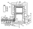
- 1 is a schematic configuration diagram of a part of a substrate processing apparatus suitably used in an embodiment of the present invention, and is a cross-sectional view of a reaction tube.
- It is a schematic block diagram of the controller of the substrate processing apparatus used suitably by embodiment of this invention.
- It is a piping block diagram of the conventional furnace port part vicinity.
- a substrate processing apparatus is configured as an example of a semiconductor manufacturing apparatus used for manufacturing a semiconductor device. Specifically, a treatment chamber composed of at least a reaction tube and a furnace port provided at the lower part of the reaction tube, a nozzle provided in the furnace port and rising from the furnace port to the inside of the reaction tube, and a nozzle A processing gas supply system provided upstream of the processing gas, a shut-off portion configured to be provided at a boundary between the processing gas supply system and the nozzle, and a gas passing from the nozzle into the processing chamber in conjunction with the processing gas supply system. And at least a controller that controls the processing gas supply system and the shutoff unit.
- the furnace port portion is configured so that a shut-off portion connected to a nozzle rising from the inner wall of the furnace port portion to the inside of the reaction tube is not provided with a pipe between the outer wall of the furnace port portion. .
- a cooling mechanism so that the shut-off valve can be cooled.
- a furnace port unit capable of local exhaust as a countermeasure against heat accumulation in the furnace port. The cooling mechanism and the furnace port unit will be described later.
- the furnace port part and the shut-off valve are integrated (for example, a pipe including a flexible pipe is not provided between the furnace port part and the shut-off valve).
- a pipe including a flexible pipe is not provided between the furnace port part and the shut-off valve.
- the processing furnace 202 includes a heater 207 as a heating unit (heating mechanism).
- the heater 207 has a cylindrical shape and is configured to include a heater wire and a heat insulating material (not shown).
- the lower part of the heater 207 is vertically installed by being supported by a heater base (not shown) as a holding plate.
- the heater 207 also functions as an activation mechanism (excitation unit) that activates (excites) the processing gas with heat.
- a reaction tube 203 having a single tube structure that constitutes a reaction vessel (processing vessel) concentrically with the heater 207 is disposed.
- the reaction tube 203 is made of a heat resistant material such as quartz (SiO 2 ) or silicon carbide (SiC).
- the reaction tube 203 is formed in a ceiling shape in which the lower end is opened and the upper end is closed with a flat wall.
- the upper end portion (hereinafter also referred to as a ceiling portion) of the reaction tube is configured to be thick from the viewpoint of ensuring strength.
- the side wall of the reaction tube 203 includes a cylindrical portion formed in a cylindrical shape, and a gas supply area 222 and a gas exhaust area 224 provided on the outer wall of the cylindrical portion.
- a processing chamber 201 is formed in the reaction tube 203 including the gas supply area 222 and the gas exhaust area 224.
- the processing chamber 201 is configured to process a wafer 200 as a substrate. Further, the processing chamber 201 is configured to be capable of accommodating a boat 217 that can hold the wafers 200 in a state where the wafers 200 are aligned in a vertical direction in multiple stages in a horizontal posture.
- the heater 207 is disposed so as to surround the reaction tube 203, and can heat the plurality of wafers 200 mounted on the boat 217 in the reaction tube 203 (or the processing chamber 201) to a predetermined temperature. it can.
- the gas supply area 222 is formed so that the convex portion protrudes outside one side wall of the cylindrical portion.
- the outer wall of the gas supply area 222 is formed outside the one side wall as a part of the outer wall of the cylindrical part of the reaction tube 203 and is concentrically formed with the cylindrical part.
- the gas supply area 222 has a ceiling shape in which the lower end is opened and the upper end is closed by a flat wall.
- nozzle portions 340a to 340c which will be described later, are accommodated along the length direction (vertical direction), and the boundary wall 254 constituting the boundary between the gas supply area 222 and the cylindrical portion has a gas.
- a supply slit 235 is formed.
- the boundary wall 254 is one side wall of the cylindrical portion, and an outer side surface thereof constitutes a side surface portion facing the gas supply area 222.
- the generic name of the nozzle portions 340a to 340c may be described as the nozzle portion 340, and the generic names of other numbers may be similarly described.
- the gas exhaust area 224 is formed so that the convex portion protrudes to the outside of the other side wall facing the one side wall where the gas supply area 222 having a cylindrical portion is formed.
- the gas exhaust area 224 is disposed so as to sandwich an area where the wafer 200 of the processing chamber 201 is accommodated between the gas exhaust area 224 and the gas supply area 222.
- the outer wall of the gas exhaust area 224 is formed outside the other side wall as a part of the outer wall of the cylindrical portion, and is concentrically formed with the cylindrical portion larger than the outer diameter of the cylindrical portion.
- the gas exhaust area 224 has a ceiling shape in which the lower end and the upper end are closed by a flat wall.
- a gas exhaust slit 236 is formed in a boundary wall 252 that is a wall body that forms a boundary between the gas exhaust area 224 and the cylindrical portion.
- the boundary wall 252 is a part of the cylindrical portion, and its outer side surface constitutes a side surface part facing the gas exhaust area 224.
- the lower end side of the reaction tube 203 is supported by a cylindrical manifold 226 as a furnace port.
- the manifold 226 is formed of a metal such as a nickel alloy or stainless steel, or a heat resistant material such as quartz (SiO 2 ) or silicon carbide (SiC).
- a flange is formed at the upper end portion of the manifold 226, and the lower end portion of the reaction tube 203 is installed and supported on the flange.
- An airtight member 220 such as an O-ring is interposed between the flange and the lower end portion of the reaction tube 203 to keep the inside of the reaction tube 203 airtight.
- a seal cap 219 is attached to the opening at the lower end of the manifold 226 through an airtight member 220 such as an O-ring, so that the opening at the lower end of the reaction tube 203, that is, the opening of the manifold 226 is airtight. It is supposed to close.
- the seal cap 219 is formed of, for example, a metal such as nickel alloy or stainless steel, and is formed in a disk shape.
- a boat support 218 that supports the boat 217 is provided on the seal cap 219.
- the boat support 218 is made of a heat-resistant material such as quartz or silicon carbide, and functions as a heat insulating portion and is a support that supports the boat 217.
- the boat 217 has a bottom plate fixed to the boat support base 218 and a top plate disposed above the bottom plate, and has a configuration in which a plurality of columns are installed between the bottom plate and the top plate. .
- the boat 217 is made of a heat resistant material such as quartz or silicon carbide.
- a boat rotation mechanism 267 that rotates the boat 217 is provided on the side of the seal cap 219 opposite to the processing chamber 201.
- the rotation shaft of the boat rotation mechanism 267 passes through the seal cap and is connected to the boat support base 218.
- the boat rotation mechanism 267 rotates the boat 217 via the boat support base 218 to rotate the wafer 200.
- the seal cap 219 is raised and lowered in the vertical direction by a boat elevator 115 as an elevating mechanism provided outside the reaction tube 203, so that the boat 217 can be carried into and out of the processing chamber 201.
- a nozzle support portion 350 that supports the nozzle portion 340 is installed in the manifold 226 so as to be bent in an L shape and penetrate the manifold 226.
- three nozzle support portions 350a to 350c are installed.
- the nozzle support part 350 is formed from materials, such as nickel alloy and stainless steel, for example.
- a gas supply pipe 310 that supplies gas into the reaction tube 203 is connected to one end of the nozzle support portion 350 on the reaction tube 203 side via a shut-off portion 101 as a shut-off valve.
- nozzle portions 340a to 340c are connected to the other ends of the nozzle support portions 350a to 350c, respectively.
- the nozzle portion 340 is formed from a heat resistant material such as quartz or SiC.
- the nozzle support part 350 and the nozzle part 340 constitute a nozzle, and the shutoff valve 101 provided at the boundary between the nozzle and the gas supply pipe 310 is fixed in the vicinity of the manifold 226.
- the nozzle shape may be a configuration in which the nozzle portion 340 and the nozzle support portion 350 are integrated.
- the nozzle part 340 is provided above the lower part in the gas supply area 222 along the length direction (vertical direction).
- the nozzle portions 340a and 340c are respectively configured as I-shaped long nozzles.
- Gas supply holes 234a and 234c for supplying gas are provided on the side surfaces of the nozzle portions 340a and 340c, respectively.
- the gas supply holes 234a and 234c are opened so as to face the center of the reaction tube 203, respectively.
- the nozzle portion 340b is configured as an I-shaped short tube nozzle (short nozzle).
- the nozzle portion 340b has an opening 234b, and the tip of the nozzle portion 340b is open.
- nozzle portions 340a to 340c are provided so that a plurality of types of gases can be supplied into the processing chamber 201.
- the shape of the nozzle portion 340 may be, for example, an L shape instead of an I shape, and is not limited to the shape.
- the boat 217 in a state where a plurality of batch-processed wafers 200 are stacked on the boat 217, the boat 217 is inserted into the processing chamber 201 while being supported by the boat support 218, and the heater 207 is installed.
- the wafer 200 inserted into the processing chamber 201 is heated to a predetermined temperature.
- the gas supply pipe 310a includes, in order from the upstream direction, a first processing gas supply source that supplies a first processing gas, a mass flow controller (MFC) 320a that is a flow rate controller (flow rate control unit), and a valve 330a that is an on-off valve.
- MFC mass flow controller
- the shut-off valve 101a is provided at the boundary between the gas supply pipe 310a and the nozzle support portion 350a, and is provided in the state of being close to the outside of the manifold 226.
- the manifold 226 and the shut-off valve 101a are integrally attached without providing a flexible pipe between the manifold 226 and the shut-off valve 101a.
- the exhaust part 102a mentioned later may be attached so that the cutoff valve 101a may be adjoined.
- the gas supply pipe 310b includes, in order from the upstream direction, a second processing gas supply source that supplies a second processing gas, a mass flow controller (MFC) 320b that is a flow rate controller (flow rate control unit), and a valve 330b that is an on-off valve.
- MFC mass flow controller
- the shut-off valve 101b is provided at the boundary between the gas supply pipe 310b and the nozzle support portion 350b, and is provided in a state of being close to the outside of the manifold 226.
- the manifold 226 and the shut-off valve 101b are integrally attached without providing a flexible pipe between the manifold 226 and the shut-off valve 101b.
- the exhaust part 102b mentioned later may be attached so that the cutoff valve 101b may be adjoined.
- the gas supply pipe 310c includes, in order from the upstream direction, a third processing gas supply source that supplies a third processing gas, a mass flow controller (MFC) 320c that is a flow rate controller (flow rate control unit), and a valve 330c that is an on-off valve.
- MFC mass flow controller
- the shut-off valve 101c is provided at the boundary between the gas supply pipe 310c and the nozzle support portion 350c, and is provided in a state close to the outside of the manifold 226.
- the manifold 226 and the shut-off valve 101c are integrally attached without providing a flexible pipe between the manifold 226 and the shut-off valve 101c.
- the exhaust part 102c mentioned later may be attached so that the cutoff valve 101c may be adjoined.
- Gas supply pipes 310d to 310f for supplying an inert gas are connected to the gas supply pipes 310a to 310c on the downstream side of the valves 330a to 330c, respectively.
- the gas supply pipes 310d to 310f are provided with MFCs 320d to 320f as flow rate controllers (flow rate control units) and valves 330d to 330f as opening / closing valves, respectively, in order from the upstream direction.
- a first process gas supply system is mainly configured by the gas supply pipe 310a, the MFC 320a, and the valve 330a. Further, the first process gas supply source, the nozzle support part 350a, the nozzle part 340a, and the shutoff valve 101a are considered to be included in the first process gas supply system, and the first process gas supply system includes the gas supply pipe 310a, the MFC 320a, and the valve 330a. It is good also as a structure containing the 1st piping part comprised by these, the 1st boundary part containing the 1st interruption
- the first processing gas supply system is configured to supply a reactive gas as the first processing gas.
- a second processing gas supply system is mainly configured by the gas supply pipe 310b, the MFC 320b, and the valve 330b. Further, the second processing gas supply source, the nozzle support portion 350b, the nozzle portion 340b, and the shutoff valve 101b are considered to be included in the second processing gas supply system, and the second processing gas supply system includes the gas supply pipe 310b, the MFC 320b, and the valve 330b. It is good also as a structure including the 2nd piping part comprised by this, the 2nd boundary part containing the 2nd interruption
- the second processing gas supply system is configured to supply a source gas as the second processing gas.
- a third processing gas supply system is mainly configured by the gas supply pipe 310c, the MFC 320c, and the valve 330c. Further, the third processing gas supply source, the nozzle support portion 350c, the nozzle portion 340c, and the shutoff valve 101c are considered to be included in the third processing gas supply system, and the third processing gas supply system includes the gas supply pipe 310c, the MFC 320c, and the valve 330c. It is good also as a structure containing the 3rd piping part comprised by these, the 3rd boundary part containing the 3rd interruption
- the third processing gas supply system is configured to supply a reactive gas or an inert gas that does not contribute to substrate processing as the third processing gas.
- the configuration of the processing gas supply system and details of the shutoff valve 101 will be described later.
- processing gas when used, it includes only the first processing gas, includes only the second processing gas, includes only the third processing gas, or includes all of them. There is.
- processing gas supply system when used, it includes only the first processing gas supply system, only the second processing gas supply system, only the third processing gas supply system, or all of them. May be included.
- An exhaust port 230 is provided below the gas exhaust area 224.
- the exhaust port 230 is connected to the exhaust pipe 232.
- the exhaust pipe 232 is evacuated through a pressure sensor 245 as a pressure detector (pressure detector) for detecting the pressure in the processing chamber 201 and an APC (Auto Pressure Controller) valve 244 as a pressure regulator (pressure adjuster).
- a vacuum pump 246 as an apparatus is connected and configured to exhaust so that the pressure in the processing chamber 201 becomes a predetermined pressure (degree of vacuum).
- the APC valve 244 can open and close the valve to stop evacuation / evacuation in the processing chamber 201, and further adjust the valve opening to adjust conductance to adjust the pressure in the processing chamber 201. It is an open / close valve.
- An exhaust system is mainly configured by the exhaust pipe 232, the APC valve 244, and the pressure sensor 245.
- a vacuum pump 246 may also be included in the exhaust system.
- the controller 280 described later executes a process recipe described later, and as described above, (A) the transport system (boat elevator 115, boat rotation mechanism 267, etc.), (B) temperature control system (heater 207, etc.). ), (C) a processing gas supply system (blocking unit 101, MFC 320, valve 330, etc.), and (D) a gas exhaust system (APC valve 244, pressure sensor 245, etc.).
- a temperature sensor 1 (hereinafter also referred to as a thermocouple) as a temperature detector is installed outside the reaction tube 203.
- the power supplied to the heater 207 is adjusted based on the temperature information detected by the temperature sensor 1 so that the temperature of the processing chamber 201 has a desired temperature distribution.
- thermocouple 1 is attached to the outside of the reaction tube 203 from a cover 2 as a protective member.
- the cover 2 is made of a quartz member.
- the thermocouple 1 is attached to the outside of the processing chamber 201 and is provided so as to face the heater 207 as a heating unit.
- the thermocouple 1 is fixed by the reaction tube 203 and the cover 2.
- thermocouples 1 Although only one thermocouple 1 is shown in FIG. 2, a plurality of thermocouples 1 may be provided. A buffer member can be provided between the thermocouple 1 and the reaction tube 203. Furthermore, although the thermocouple 1 of FIG. 2 is provided on the side wall of the reaction tube, the thermocouple 1 may be provided on the ceiling of the reaction tube 203.
- FIGS. 5 and 6 are schematic views for explaining the processing gas supply system in the present embodiment. 5 and 6 show two processing gas supply systems in FIG. 1 in order to make the explanation of the relationship among the gas supply pipe 310, the boundary portion (the shutoff valve 101) and the nozzle easier to understand. Is. Then, the controller 280 is configured to execute a process recipe to be described later and to control (C) the processing gas supply system (the shut-off unit 101, the exhaust unit 102, the switching unit 103, and the like). Further, a processing gas supply system including a processing gas supply source, an MFC 320, a valve 330, and the like is provided on the upstream side of the switching unit (switching valve), but is omitted in FIGS.
- a valve (switching valve) closest to the furnace opening in the gas box is a valve that switches between a gas that contributes to substrate processing and a cleaning gas.
- a processing gas supply system (not shown) and a cleaning gas supply system (not shown) are provided on the upstream side of the switching unit (switching valve).
- the gas supply system in this embodiment is for switching to switch between a nozzle rising from the furnace port 226 to the inside of the reaction tube 203, a boundary including at least the blocking unit 101, a gas contributing to substrate processing, and a cleaning gas.
- a gas supply pipe 310 provided with a switching unit composed of a valve (switching valve) 103, and the boundary is connected to the gas supply pipe 310, and the gas between the switching unit and the blocking unit 101 It is preferable to provide an exhaust unit 102 which will be described later for exhausting the supply pipe including the supply pipe 310.
- a processing gas supply system having a nozzle (first nozzle and second nozzle) rising from the furnace port portion 226 to the inside of the reaction tube and a gas supply pipe 310a provided on the upstream side of the nozzle (first nozzle).
- First gas supply system a processing gas supply system (second gas supply system) having a gas supply pipe 310b provided upstream of the nozzle (second nozzle), a first nozzle and a first gas supply system.
- a blocking unit 101a (first blocking unit) configured to be provided at the boundary
- a 101b (second blocking unit) configured to be provided at the boundary between the second nozzle and the second gas supply system
- the first A reaction gas is supplied as a first gas in the reaction tube by interlocking the shut-off portion with the first gas supply system
- a raw material is supplied as a second gas in the reaction tube by interlocking the second shut-off portion with the second gas supply system. It is configured to supply gas.
- the first gas supply system, the first blocking unit, the second gas supply system, and the second blocking unit are configured to be controlled by the controller 280 in FIGS. 5 and 6.
- the first process gas is supplied from the gas supply pipe 310a through the first nozzle by providing the cutoff valve 101 (boundary portion), opening the cutoff valve 101a, and closing the cutoff valve 101b.
- the gas supply pipe 310b and the reaction pipe 203 can be shut off to suppress the reverse diffusion of the first processing gas into the gas supply pipe 310b, while the shutoff valve 101b is opened and the shutoff valve 101a is closed.
- the gas supply pipe 310a and the reaction tube 203 are shut off to suppress back diffusion of the first processing gas into the gas supply pipe 310a. Can do.
- the shutoff valve 101a is closed while the shutoff valve 101b is opened and the source gas is supplied into the reaction tube 203 from the second nozzle.
- the gas supply pipe 310a and the reaction pipe 203 are shut off, and the back diffusion of the source gas into the gas supply pipe 310a can be completely suppressed. Particles can be reduced.
- a furnace port box for performing local exhaust of the furnace port part 226 may be provided so as to surround the furnace port part 226.
- the furnace port box is used for countermeasures against gas leaks and heat accumulation in the furnace port part 226.
- the inside of the furnace port box has a high temperature atmosphere of 50 ° C to 200 ° C.
- the heat resistant temperature of the valve is about 150 ° C.
- it is conceivable to use a heat resistant specification valve heat resistant temperature 250 to 300 ° C.
- the operating life of the heat resistant specification valve is significantly reduced and the replacement frequency is shortened.
- the valve can be arranged in the furnace port box even when the heat resistance temperature of the valve is exceeded.
- a heat dissipation method using cooling water for example, a configuration in which the shutoff valve 101 is covered with a cooling block
- Any cooling method may be used as long as it can be set to a temperature lower than the heat resistant temperature of the valve.
- an exhaust system for discharging the gas in the reaction tube 203 is provided, and the control unit 280 closes the first blocking unit and the second blocking unit when the supply of the reaction gas or the raw material gas to the substrate in the reaction tube 203 is completed.
- the exhaust system is controlled to discharge the unreacted source gas or reaction gas from the reaction tube 203.
- the control unit 280 opens the first gas supply system so as to perform the cycle purge by changing the flow rate of the inert gas supplied into the reaction tube 203 in a state where the first blocking unit and the second blocking unit are opened.
- the first blocking unit, the second gas supply system, the second blocking unit, and the exhaust system are configured to be controlled.
- the gas supply pipe 310 between the switching part and the boundary part is configured to include a flexible pipe whose shape can be bent.
- the flexible pipe is provided in the gas supply pipe 310, and may be, for example, a bellows shape.
- blocking part 101 is installed in the side wall of the furnace port part 226 by the integral type (or direct connection).
- flexible piping is provided in the furnace port box.
- the flexible pipe is not provided in this form, but is provided in the pipe between the gas box provided with the switching unit and the furnace port box provided with the blocking unit 101.
- the site for example, a semiconductor factory
- the metal and the pipe for example, metal
- the piping installed between the furnace port portion 226 and the switching unit has been configured to include flexible piping, but in this embodiment, the piping between the furnace port portion 226 and the shut-off unit 101.
- the piping installed between them does not include flexible piping.
- the gas supply pipe 310 is provided on the upstream side of the blocking unit 101, but the flexible pipe provided in the gas supply pipe 310 is omitted.
- FIG. 6 is a schematic diagram illustrating a configuration in which an exhaust unit 102 is further provided so as to be adjacent to the blocking unit 101 of the gas supply system illustrated in FIG. 5.
- an exhaust unit 102 that branches the supply pipe is installed on the upstream side of the blocking unit 101, and a vent pipe is connected to the exhaust pipe 232 by the exhaust unit 102. Due to such a configuration, the gas supply pipe 310 including the flexible pipe between the switching unit and the blocking unit 101 can be cycle purged without using the reaction tube 203.
- the gas supply pipe 310a can be cycle purged when the source gas is supplied from the gas supply pipe 310b into the reaction tube 203, and the cleanliness in the gas supply pipe 310a is further improved. Can be improved.
- the gas supply tube 310 can be individually cycle purged, and the gas supply tube 310 can be further purged. Cleanliness can be improved.
- the space around the manifold 226 is small due to the configuration of the apparatus, and it is difficult to install the shut-off part 101 and the exhaust part 102. This can be realized, and improvement in maintainability can be achieved.
- shut-off valve 101 provided close to the outside of the furnace port portion 226 will be described in detail mainly using FIGS. 7 to 10.
- the configuration between the furnace port portion 226 and the shut-off portion 101 in the present embodiment is a configuration in which the furnace port portion 226 and the shut-off valve 101 are directly connected as shown in FIG.
- the furnace port 226 and the shut-off valve 101a (101b) may have an integrated configuration (a configuration in which no piping is provided in appearance).
- 7 and 8 are also diagrams showing the furnace port portion 226 to which the blocking portion 101 is added.
- the exhaust port 102 can be integrated with the furnace port unit 226 in a state where the exhaust unit 102 is adjacent to the blocking unit 101.
- the blocking unit 101 may be configured with a cooling mechanism.
- the length of the piping (pipe length) installed between the furnace port portion 226 and the switching portion in FIG. 4 and the piping installed between the furnace port portion 226 and the blocking portion 101 in the present embodiment. Compare the length (pipe length). Assuming that the pipe length of the embodiment of FIG. 7 is 100 mm, the length ratio of the pipe length is about 1/5 to 1/30. Furthermore, in the embodiment of FIG. When included in the pipe, it is assumed that the length is approximately 50 mm, and the length ratio of the pipe length is about 1/10 to 1/60. Also, the ideal pipe length is zero (a configuration in which no pipe is provided).
- FIG. 10 shows the details of the configuration in which the shut-off portion 101 is integrally attached to the furnace port portion 226 in FIG. 8, that is, the shut-off portion 101 attached so as not to provide piping on the side wall of the furnace port portion 226.
- blocking part 101 is not shown in FIG. 10, it is provided in the multiple furnace opening part 226 by the same structure.
- the shut-off part 101 is connected to a nozzle (or nozzle support part 350) disposed inside the furnace port part 226 at one end, and is connected to a pipe (in this embodiment, a gas supply pipe) outside the furnace port part 226 at the other end.
- 10 is a diagram when the blocking unit 101 is in an open state, in which the gas flow path communicates from the gas supply pipe 310 to the nozzle unit 340 through the blocking unit 101. It is configured.
- the controller 280 which is a control unit (control means), is configured as a computer having a CPU (Central Processing Unit) 121a, a RAM (Random Access Access Memory) 121b, a storage device 121c, and an I / O port 121d.
- the RAM 121b, the storage device 121c, and the I / O port 121d are configured to exchange data with the CPU 121a via the internal bus 121e.
- an input / output device 122 configured as a touch panel or the like is connected to the controller 280.
- the storage device 121c is configured by, for example, a flash memory, an HDD (Hard Disk Drive), or the like.
- a control program for controlling the operation of the substrate processing apparatus, a film forming sequence to be described later as a process recipe describing the procedure and conditions of the substrate processing, and the like are stored in a readable manner.
- the process recipe is a combination of functions so that a predetermined result can be obtained by causing the controller 280 to execute each procedure in the substrate processing process described later, and functions as a program.
- the process recipe, the control program, and the like are collectively referred to simply as a program.
- the RAM 121b is configured as a memory area (work area) in which programs, data, and the like read by the CPU 121a are temporarily stored.
- the I / O port 121d includes the above-described MFCs 320a to 320f, valves 330a to 330f, shutoff valves 101a to 101c, exhaust valves 102a to 102c, pressure sensor 245, APC valve 244, vacuum pump 246, heater 207, temperature sensor (thermocouple) ) 1, connected to the boat rotation mechanism 267, the boat elevator 115, and the like.
- the CPU 121a is configured to read out and execute a control program from the storage device 121c, and to read out a process recipe from the storage device 121c in response to an operation command input from the input / output device 122 or the like.
- the CPU 121a adjusts the flow rates of various gases by the MFCs 320a to 320f, the opening and closing operations of the valves 330a to 330f, the opening and closing operations of the shutoff valves 101a to 101c, and the opening and closing of the APC valve 244 in accordance with the contents of the read control program and process recipe.
- the boat elevator 115 is configured to control the lifting and lowering operation of the boat 217 and the like.
- the controller 280 is stored in an external storage device 123 (for example, a magnetic tape, a magnetic disk such as a flexible disk or a hard disk, an optical disk such as a CD or DVD, a magneto-optical disk such as an MO, or a semiconductor memory such as a USB memory or a memory card).
- an external storage device 123 for example, a magnetic tape, a magnetic disk such as a flexible disk or a hard disk, an optical disk such as a CD or DVD, a magneto-optical disk such as an MO, or a semiconductor memory such as a USB memory or a memory card.
- the above-mentioned program can be executed.
- the storage device 121c and the external storage device 123 can be configured as computer-readable recording media. Hereinafter, these are collectively referred to simply as a recording medium.
- the term “recording medium” may include only the storage device 121c alone, may include only the external storage device 123 alone, or may include both.
- the substrate processing apparatus is controlled by the controller 280.
- a boat 217 on which a predetermined number of wafers 200 are placed is inserted into the reaction tube 203, and the reaction tube 203 is hermetically closed by a seal cap 219.
- the wafer 200 is heated to be maintained at a predetermined temperature, and a processing gas is supplied into the reaction tube 203 so that the wafer 200 is subjected to heat treatment such as heating.
- a film forming sequence shown in FIG. 11 as a process recipe is supplied to the wafer 200 in the processing chamber 201, and the HCDS gas from the processing chamber 201 is supplied.
- a step of removing the gas (residual gas) a step of supplying NH 3 gas to the wafer 200 in the processing chamber 201, and a step of removing the NH 3 gas (residual gas) from the processing chamber 201.
- the SiN film is formed on the wafer 200 by performing the simultaneous cycle a predetermined number of times (one or more times).
- substrate is synonymous with the use of the term “wafer”.
- the inside of the processing chamber 201 that is, the space where the wafer 200 exists, is evacuated to a vacuum by a vacuum pump 246 so that a predetermined pressure (degree of vacuum) is obtained.
- a predetermined pressure degree of vacuum
- the vacuum pump 246 maintains a state in which it is always operated until at least the processing on the wafer 200 is completed.
- the wafer 200 in the processing chamber 201 is heated by the heater 207 so as to reach a predetermined temperature.
- the power supply to the heater 207 is feedback-controlled based on the temperature information detected by the temperature sensor so that the processing chamber 201 has a predetermined temperature distribution. Heating of the processing chamber 201 by the heater 207 is continuously performed at least until the processing on the wafer 200 is completed.
- the rotation of the boat 217 and the wafers 200 by the rotation mechanism 267 is started.
- the wafer 200 is rotated.
- the rotation of the boat 217 and the wafer 200 by the rotation mechanism 267 is continuously performed at least until the processing on the wafer 200 is completed.
- Step 1 a source gas (HCDS gas) is supplied to the wafer 200 in the processing chamber 201.
- This step 1 includes at least a pre-purge process, a source gas supply process, a source gas exhaust process, and a purge process.
- HCDS gas a source gas
- the valves 330b and 330e are opened, and HCDS gas is caused to flow into the gas supply pipe 310b.
- the shut-off valve 101b is closed and not supplied to the processing chamber 201.
- the valves 330d and 330f are simultaneously opened, and N 2 gas is allowed to flow into the gas supply pipes 310a and 310c.
- the shutoff valves 101 a and 101 c may be opened, and N 2 gas may be supplied into the processing chamber 201 at a predetermined flow rate adjusted by the MFC and exhausted from the exhaust pipe 232.
- the exhaust valve 102b is provided adjacent to the shutoff valve 101b, the exhaust valve 102b is opened, and the HCDS gas can be exhausted from the gas supply pipe 310b to the exhaust pipe 232 via the exhaust valve 102b. Is preferred.
- shutoff valve 101b is closed with the shutoff valves 101a and 101c being closed.
- the APC valve 244 is kept open, and the inside of the processing chamber 201 is evacuated by the vacuum pump 246 to form a silicon (Si) -containing layer as an unreacted or first layer remaining in the processing chamber 201.
- the contributed HCDS gas is discharged from the processing chamber 201.
- the source gas supply step and the source gas exhaust step are sequentially executed (three times in this embodiment). At this time, the first layer is formed on the outermost surface of the wafer 200.
- the HCDS gas is supplied to the processing chamber 201 by a short tube nozzle whose tip is opened, and in order to make the gas concentration distribution uniform, such a cyclic supply (cycle Flow).
- the gas supply method is appropriately set according to the nozzle shape.
- valve 330b After purge process, the valve 330b is closed and the supply of HCDS gas is stopped. At this time, the valves 330d to 330f and the shutoff valves 101a to 101c are opened, and the supply of N 2 gas into the processing chamber 201 is resumed.
- the N 2 gas acts as a purge gas, whereby the effect of exhausting the gas remaining in the processing chamber 201 from the processing chamber 201 can be enhanced.
- Step 1 a gas purge step for reliably discharging the gas remaining in the processing chamber 201 from the processing chamber 201 before supplying the reaction gas is included in Step 1, but the film forming sequence is shown in FIG. You may divide from 1 to step 4. FIG. 13 will be described later.
- Step 2 After Step 1 is completed, NH 3 gas is supplied as a reaction gas to the wafer 200 in the processing chamber 201, that is, the first layer formed on the wafer 200.
- the NH 3 gas is activated by heat and supplied to the wafer 200.
- the opening / closing control of the valves 330a, 330d, 101a is performed in the same procedure as the opening / closing control of the valves 330b, 330e, 101b in step 1.
- the flow rate of NH 3 gas is adjusted by MFC, and the NH 3 gas is supplied into the processing chamber 201 through the nozzle unit 340 a and exhausted from the exhaust pipe 232.
- NH 3 gas is supplied to the wafer 200.
- the NH 3 gas supplied to the wafer 200 reacts with at least a part of the first layer, that is, the Si-containing layer formed on the wafer 200 in Step 1.
- the first layer is thermally nitrided by non-plasma and is changed (modified) into a second layer containing Si and N, that is, a silicon nitride layer (SiN layer).
- a second layer containing Si and N that is, a silicon nitride layer (SiN layer).
- plasma-excited NH 3 gas is supplied to the wafer 200, and the first layer is plasma-nitrided to change the first layer to the second layer (SiN layer). May be.
- the valves 330a and 330d are closed, and the supply of NH 3 gas is stopped. Then, the NH 3 gas and the reaction by-product remaining in the processing chamber 201 and contributed to the formation of the second layer are discharged from the processing chamber 201 by the same processing procedure as in Step 1.
- Step 2 includes a step of reliably discharging the gas remaining in the processing chamber 201 from the processing chamber 201 after supplying the reaction gas.
- the procedure is to open the valves 330d to 330f and the shut-off valves 101a to 101c, continue supplying N 2 gas into the processing chamber 201, and vary the flow rate at a predetermined cycle. For example, switching between the flow rate A and the flow rate B (flow rate A> flow rate B) is performed a predetermined number of times. In the present embodiment, control is performed four times.
- the purge process is completed by supplying N 2 gas adjusted to a predetermined flow rate into the processing chamber 201 for a predetermined time with the valves 330d to 330f and the shutoff valves 101a to 101c being opened. This completes the film forming sequence.
- SiN having a predetermined composition and a predetermined film thickness is formed on the wafer 200.
- a film can be formed.
- the above cycle is preferably repeated a plurality of times. That is, it is formed by stacking the second layer (SiN layer) by making the thickness of the second layer (SiN layer) formed when the above cycle is performed once smaller than a predetermined thickness.
- the above cycle is preferably repeated a plurality of times until the thickness of the SiN film reaches a predetermined thickness.
- the processing gas supply for supplying the HCDS gas By closing the shut-off valve 101 connected to the processing gas supply system other than the system, the HCDS gas is not diffused into other processing gas supply systems. Accordingly, particles caused by by-products in the piping such as the gas supply pipe 310 can be reduced.
- the pipes constituting the processing gas supply system for supplying HCDS gas are heated.
- the range to be performed can be greatly reduced.
- the processing gas supply system other than the processing gas supply system for supplying the HCDS gas similarly heated the piping through which the HCDS gas is diffused.
- the gas it is not necessary to heat the piping, Even if it is a necessary gas, it may be heated to an appropriate temperature, and the range heated up to now to prevent liquefaction of HCDS can be reduced, leading to a reduction in heater costs.
- FIG. 12 is a diagram showing the N2 gas flow rate dependency obtained by changing the flow rate of the counter N2 from two systems other than the film forming gas supply system in the processing gas supply system (three systems) shown in FIG.
- Temperature of wafer 200 100 to 800 ° C. (preferably 400 to 750 ° C., in this embodiment, 630 ° C.) Processing chamber pressure: 5 to 4000 Pa (preferably 10 to 1332 Pa) HCDS gas supply flow rate: 1 to 2000 sccm (preferably 50 to 500 sccm) NH 3 gas supply flow rate: 100-30000 sccm N 2 gas supply flow rate: 1 to 50000 sccm SiN film thickness: 0.2 to 100 nm
- FIG. 12 is a table comparing the film thickness average value and in-plane uniformity of the wafer 200 arranged at each of the TOP, CNT, and BTM positions in the substrate processing region with respect to the presence / absence of the counter N2 and the flow rate. Moreover, it is the table
- the absence of the counter N2 shown in FIG. 12 corresponds to this embodiment. That is, according to the present embodiment, the shutoff valve 101 provided in the gas supply system that has been supplying the counter N2 into the processing chamber 201 is closed while the HCDS gas and the NH3 gas are being supplied. As a result, the HCDS gas and NH3 gas can be prevented from back-diffusion on the gas supply pipe 310 side, so that the counter N2 is not necessary.
- the average film thickness of the wafer 200 arranged at each of the TOP, CNT, and BTM positions in the substrate processing region is the highest. This is because the concentration of the HCDS gas and NH 3 gas in the processing chamber 201 is high because the counter N2 does not need to be diluted.
- the in-plane uniformity of the wafer 200 disposed at each of the TOP, CNT, and BTM positions in the substrate processing region is the lowest value. This is because the HCDS gas and NH 3 gas in the processing chamber 201 can contact the surface of the wafer 200 evenly (or entirely) without being affected by the counter N2.
- TOP is the wafer 200 disposed at the top of the wafers 200 disposed in the substrate processing region
- BTM is the wafer 200 disposed at the bottom of the wafers 200 disposed in the substrate processing region
- the CNT is the wafer 200 arranged at the center of the wafers 200 arranged in the substrate processing region. For example, if a dummy wafer (side dummy wafer) is placed in Slots 1 to 4 and Slots 30 to 33 in a mini-batch furnace (all 33 slots), TOP: 29 Slot, CNT: 17 Slot, and BTM: 5 Slot.
- the in-plane uniformity is averaged by measuring the film thickness at a predetermined location in the wafer 200 plane.
- the inter-surface uniformity is calculated by obtaining the average value for the number of wafers 200 placed in the slots from TOP to BTM. According to the mini-batch furnace, the inter-plane average value is calculated from the in-plane average value for 25 slots.
- FIG. 13 shows a comparison between a current film forming sequence without a shut-off valve and a film forming sequence in an embodiment having a shut-off valve. Obviously, the time required for gas replacement in the reaction tube is greatly improved in the purge process (gas replacement process) after supplying the processing gas.
- the time required for one cycle of the current film forming sequence is 51 sec
- the time required for one cycle of the film forming sequence in the present embodiment having the shut-off valve 101 is 41 sec. Therefore, it can be shortened by about 20% (10 sec) in one cycle.
- the gas replacement efficiency in the reaction tube can be greatly improved by closing the shutoff valve in the purging step after supplying the processing gas. Accordingly, it is possible to shorten the time related to the purge process in the film forming sequence. Further, throughput can be improved by shortening the film forming sequence.
- shutoff valve is configured to be provided close to the side wall of the furnace port portion, while the processing gas is being supplied from the other gas supply pipe into the reaction pipe, By closing the shut-off valve, back diffusion of the processing gas into the gas supply pipe can be suppressed.
- the pipe heating range can be reduced and each pipe heating temperature can be optimized.
- the temperature of the gas supply pipe is set to the temperature of the gas supply pipe even when the required temperature uniformity is not as high as the gas supply pipe. It was necessary to set, but by adding a shut-off valve, it is not necessary to improve the temperature uniformity as high as the gas supply pipe, and an inexpensive, relatively low temperature heater or a heater with a simple heat insulation structure is selected. be able to.
- the gas replacement efficiency in the processing chamber can be improved and the film forming sequence time can be shortened by closing the shut-off valve and suppressing the gas back diffusion upstream of the supply gas pipe.
- a vertical semiconductor manufacturing apparatus which is a kind of substrate processing apparatus has been described in detail.
- the present invention is not limited to this, and the present invention can be applied to, for example, a horizontal semiconductor manufacturing apparatus.
- HCDS gas in addition to HCDS gas, monochlorosilane (SiH 3 Cl, abbreviation: MCS) gas, dichlorosilane (SiH 2 Cl 2 , abbreviation: DCS) gas, trichlorosilane (SiHCl 3 , abbreviation: TCS) gas
- MCS monochlorosilane
- DCS dichlorosilane
- TCS trichlorosilane
- Inorganic halosilane source gases such as tetrachlorosilane, that is, silicon tetrachloride (SiCl 4 , abbreviation: STC) gas, octachlorotrisilane (Si 3 Cl 8 , abbreviation: OCTS) gas, and trisdimethylaminosilane (Si [N (CH 3 ) 2 ] 3 H, abbreviation: 3DMAS) gas, tetrakis
- the source gas contains no halogen group such as monosilane (SiH 4 , abbreviation: MS) gas, disilane (Si 2 H 6 , abbreviation: DS) gas, trisilane (Si 3 H 8 , abbreviation: TS) gas, etc.
- An inorganic silane source gas can be used.
- NH 3 gas is used as the reaction gas.
- the present invention is not limited to such an embodiment.
- hydrogen nitride-based gas such as diazene (N 2 H 2 ) gas, hydrazine (N 2 H 4 ) gas, N 3 H 8 gas, or a gas containing these compounds Etc. can be used.
- MEA gas such as ethylamine gas, trimethylamine ((CH 3 ) 3 N, abbreviation: TMA) gas, dimethylamine ((CH 3 ) 2 NH, abbreviation: DMA) gas, monomethylamine (CH 3 NH) 2 , abbreviation: MMA) methylamine gas such as gas
- an organic hydrazine-based gas such as trimethylhydrazine ((CH 3 ) 2 N 2 (CH 3 ) H, abbreviation: TMH) gas can be used.
- the SiN film is formed using HCDS gas as the source gas and nitrogen (N) -containing gas (nitriding gas) such as NH 3 gas as the reaction gas has been described.
- nitrogen (N) -containing gas such as NH 3 gas
- the present invention is not limited to such an embodiment.
- oxygen (O) containing gas oxygen (O 2 ) gas, carbon (C) containing gas such as propylene (C 3 H 6 ) gas, trichloride
- a boron (B) -containing gas such as boron (BCl 3 ) gas or the like
- a SiO film, a SiON film, a SiOCN film, a SiOC film, a SiCN film, a SiBN film, a SiBCN film, or the like can be formed.
- the order which flows each gas can be changed suitably. Even in the case where these films are formed, the film formation can be performed under the same processing conditions as in the above-described embodiment, and the same effect as in the above-described embodiment can be obtained.
- the order in which each gas flows can be changed as appropriate. Even in the case where these films are formed, the film formation can be performed under the same processing conditions as in the above-described embodiment, and the same effect as in the above-described embodiment can be obtained. That is, the present invention can be suitably applied when forming a film containing a predetermined element such as a semiconductor element or a metal element.
- the present invention is not limited to such an embodiment.
- the present invention can also be suitably applied to a case where a process such as an oxidation process, a diffusion process, an annealing process, or an etching process is performed on a substrate or a film formed on the substrate.
- a process such as an oxidation process, a diffusion process, an annealing process, or an etching process is performed on a substrate or a film formed on the substrate.
- the above-described embodiments and modifications can be used in appropriate combination.
- the processing conditions at this time can be set to the same processing conditions as in the above-described embodiment or modification, for example.
- the present invention can be applied to a substrate processing apparatus for forming a film on a substrate.
Landscapes
- Chemical & Material Sciences (AREA)
- Chemical Kinetics & Catalysis (AREA)
- General Chemical & Material Sciences (AREA)
- Engineering & Computer Science (AREA)
- Materials Engineering (AREA)
- Mechanical Engineering (AREA)
- Metallurgy (AREA)
- Organic Chemistry (AREA)
- Inorganic Chemistry (AREA)
- Chemical Vapour Deposition (AREA)
- Formation Of Insulating Films (AREA)
Abstract
Description
本発明は、基板処理装置、炉口部および半導体装置の製造方法並びにプログラムに関する。 The present invention relates to a substrate processing apparatus, a furnace opening, a method for manufacturing a semiconductor device, and a program.
基板処理装置の一例としての半導体製造装置には、縦型装置があることが知られている。昨今、この種の半導体製造装置は、多様な成膜を可能にする為に開閉弁(バルブ)の個数も多く、ガス供給系も2系統以上の場合が多い。従来、図4に示すように、炉口部に最も近い開閉弁から炉口部までの配管は、フレキシブル配管を含む配管となっていた。装置のレイアウトにもよるが、この配管の長さは、500~3000mm程度であった。 It is known that a semiconductor manufacturing apparatus as an example of a substrate processing apparatus includes a vertical apparatus. In recent years, this type of semiconductor manufacturing apparatus has a large number of on-off valves (valves) and a gas supply system of two or more systems in order to enable various film formation. Conventionally, as shown in FIG. 4, the piping from the on-off valve closest to the furnace opening to the furnace opening is a pipe including a flexible pipe. Although depending on the layout of the apparatus, the length of this pipe was about 500 to 3000 mm.
この開閉弁までのフレキシブル配管を含む配管内に付着した副生成物が起因とされるパーティクルが反応室内に放出され基板上に付着することでデバイス特性に影響を与えることが知られている。そこで、この問題を防止する手段として、成膜ガスを供給していない配管に、N2ガスを成膜ガスの供給と同時に流す方法が、実施されている。ところが、このN2ガス(以後、カウンターN2ガスという場合がある)を供給することにより成膜ガス濃度が、反応室内で不均一となり、基板処理において膜厚均一性が悪化してしまう。
It is known that particles attributed to by-products adhering to the piping including the flexible piping up to the on-off valve are emitted into the reaction chamber and adhere to the substrate, thereby affecting the device characteristics. Therefore, as a means for preventing this problem, a method of flowing N2 gas simultaneously with the supply of the film forming gas into a pipe to which the film forming gas is not supplied has been implemented. However, by supplying this
ここで、カウンターN2ガスを不要にする構成として、ガス供給系内の処理炉に近い配管に開閉弁を設置することが考えられるが、弁設置スペース制限、弁耐熱温度制限等の原因で実現できていない。一方、特許文献1及び特許文献2のように、開閉弁が炉口部の近くの配管に設けられる構成が図示されている。但し、これら先行技術文献には、カウンターN2ガスを不要にする構成については言及されていない。
Here, as a configuration that eliminates the need for the counter N2 gas, it is conceivable to install an on-off valve in a pipe close to the processing furnace in the gas supply system. Not. On the other hand, as shown in
本発明の目的は、上記問題点を解決するために、炉口部の近傍に開閉弁を設ける構成を提供することである。 In order to solve the above problems, an object of the present invention is to provide a configuration in which an on-off valve is provided in the vicinity of a furnace port portion.
本発明の一態様によれば、反応管と該反応管の下部に設けられる炉口部で少なくとも構成される処理室と、前記炉口部に設けられ、前記炉口部から前記反応管内まで立上ったノズルと、前記ノズルの上流側に設けられるガス供給系と、前記ガス供給系と前記ノズルの境界に設けられるよう構成されている遮断部と、前記遮断部を前記ガス供給系と連動させて前記ノズルから前記処理室内にガスを供給するよう、前記ガス供給系及び前記遮断部をそれぞれ制御する制御部と、を備えた構成が提供される。 According to one aspect of the present invention, a treatment chamber configured at least by a reaction tube and a furnace port provided at a lower portion of the reaction tube, and provided in the furnace port, and stands from the furnace port to the inside of the reaction tube. An up nozzle, a gas supply system provided on the upstream side of the nozzle, a shut-off part configured to be provided at a boundary between the gas supply system and the nozzle, and the shut-off part interlocked with the gas supply system And a control unit for controlling the gas supply system and the blocking unit so as to supply gas from the nozzle into the processing chamber.
本発明によれば、炉口部の近傍に開閉弁が取り付けられた構成を提供することができる。 ADVANTAGE OF THE INVENTION According to this invention, the structure by which the on-off valve was attached to the vicinity of the furnace port part can be provided.
<本発明の一実施形態>
本発明の一実施形態における基板処理装置は、半導体装置の製造に使用される半導体製造装置の一例として構成されているものである。具体的には、反応管と該反応管の下部に設けられる炉口部で少なくとも構成される処理室と、炉口部に設けられ、炉口部から反応管内まで立上ったノズルと、ノズルの上流側に設けられる処理ガス供給系と、該処理ガス供給系とノズルの境界に設けられるよう構成されている遮断部と、遮断部を処理ガス供給系と連動させてノズルから処理室内にガスを供給するよう、処理ガス供給系及び遮断部をそれぞれ制御するコントローラと、を少なくとも有する構成である。
<One Embodiment of the Present Invention>
A substrate processing apparatus according to an embodiment of the present invention is configured as an example of a semiconductor manufacturing apparatus used for manufacturing a semiconductor device. Specifically, a treatment chamber composed of at least a reaction tube and a furnace port provided at the lower part of the reaction tube, a nozzle provided in the furnace port and rising from the furnace port to the inside of the reaction tube, and a nozzle A processing gas supply system provided upstream of the processing gas, a shut-off portion configured to be provided at a boundary between the processing gas supply system and the nozzle, and a gas passing from the nozzle into the processing chamber in conjunction with the processing gas supply system. And at least a controller that controls the processing gas supply system and the shutoff unit.
また、炉口部は、炉口部の内壁から反応管内まで立上ったノズルに接続される遮断部が、炉口部の外壁との間に配管を設けないよう取付けられるよう構成されている。このように、処理炉のほぼ真下(炉口部近傍)に遮断部が取り付けられるので、冷却機構を備え、遮断弁を冷却できるようにするのが好ましい。また、炉口部の熱こもり対策として、特に局所的な排気が可能な炉口ユニットを設けるのが好ましい。尚、これら冷却機構及び炉口ユニットについては後述する。 Further, the furnace port portion is configured so that a shut-off portion connected to a nozzle rising from the inner wall of the furnace port portion to the inside of the reaction tube is not provided with a pipe between the outer wall of the furnace port portion. . As described above, since the shut-off part is attached almost directly below the processing furnace (near the furnace port part), it is preferable to provide a cooling mechanism so that the shut-off valve can be cooled. Moreover, it is preferable to provide a furnace port unit capable of local exhaust as a countermeasure against heat accumulation in the furnace port. The cooling mechanism and the furnace port unit will be described later.
ここで、本実施形態において、炉口部と遮断弁とを一体とした(例えば、炉口部と遮断弁との間にフレキシブル配管を含む配管を設けない)構造のことを単に炉口部と呼ぶ場合がある。 Here, in the present embodiment, the furnace port part and the shut-off valve are integrated (for example, a pipe including a flexible pipe is not provided between the furnace port part and the shut-off valve). Sometimes called.
以下、本発明の実施形態について、図1、図2等を用いて説明する。先ず、図1に示すように、処理炉202は加熱部(加熱機構)としてのヒータ207を有する。ヒータ207は円筒形状であり、図示しないがヒータ素線と断熱材を含むような構成である。ヒータ207の下部は、保持板としてのヒータベース(図示せず)に支持されることにより垂直に据え付けられる。また、ヒータ207は、処理ガスを熱で活性化(励起)させる活性化機構(励起部)としても機能する。
Hereinafter, an embodiment of the present invention will be described with reference to FIGS. First, as shown in FIG. 1, the
ヒータ207の内側には、ヒータ207と同心円状に反応容器(処理容器)を構成する単管構造の反応管203が配設されている。反応管203は、例えば石英(SiO2)または炭化シリコン(SiC)等の耐熱性材料から形成されている。反応管203は、下端部が開放され、上端部が平坦状の壁体で閉塞された有天井の形状で形成されている。反応管の上端部(以後、天井部ともいう)は、強度の確保という観点から厚く構成されている。反応管203の側壁は、円筒形状に形成された円筒部と、円筒部の外壁に設けられたガス供給エリア222とガス排気エリア224とを備えている。ガス供給エリア222とガス排気エリア224を含む反応管203の内部には、処理室201が形成されている。処理室201は、基板としてのウエハ200を処理可能に構成されている。また、処理室201は、ウエハ200を水平姿勢で垂直方向に多段に整列した状態で保持可能なボート217を収容可能に構成されている。そして、ヒータ207は反応管203を囲繞するように配置されており、反応管203(若しくは処理室201)内のボート217に載置された複数枚のウエハ200を所定の温度に加熱することができる。
Inside the
ガス供給エリア222は、凸部が円筒部の一側壁の外側に突出するように形成されている。ガス供給エリア222の外壁は、反応管203の円筒部の外壁の一部としての一側壁の外側に円筒部の外径よりも大きく、円筒部と同心円状に形成されている。ガス供給エリア222は、下端部が開放され、上端部が平坦状の壁体で閉塞された有天井の形状で構成されている。ガス供給エリア222には、その長さ方向(上下方向)に沿って後述するノズル部340a~340cが収容され、ガス供給エリア222と円筒部との間の境界を構成する境界壁254にはガス供給スリット235が形成されている。境界壁254は円筒部の一側壁であって、その外側面は、ガス供給エリア222に面する側面部分を構成する。以後、例えば、ノズル部340a~340cの総称を、ノズル部340と記載する場合があり、また、他の番号についても総称は同様に記載する場合がある。
The
ガス排気エリア224は、凸部が円筒部のガス供給エリア222が形成された一側壁に対向する他側壁の外側に突出するように形成されている。ガス排気エリア224は、ガス供給エリア222との間に処理室201のウエハ200が収容される領域を挟むように配置されている。ガス排気エリア224の外壁は、円筒部の外壁の一部としての他側壁の外側に円筒部の外径よりも大きく、円筒部と同心円状に形成されている。ガス排気エリア224は、下端部と上端部が平坦状の壁体で閉塞された有天井の形状で構成されている。ガス排気エリア224と円筒部との間の境界を構成する壁体である境界壁252にはガス排気スリット236が形成されている。境界壁252は円筒部の一部であって、その外側面は、ガス排気エリア224に面する側面部分を構成する。
The
反応管203の下端側は、炉口部としての円筒体状のマニホールド226によって支持されている。マニホールド226は、例えばニッケル合金やステンレス等の金属で形成されるか、若しくは石英(SiO2)または炭化シリコン(SiC)等の耐熱性材料で形成されている。マニホールド226の上端部にはフランジが形成されており、このフランジ上に反応管203の下端部を設置して支持する。このフランジと反応管203の下端部との間にはOリング等の気密部材220を介在させて反応管203内を気密状態にしている。
The lower end side of the
マニホールド226の下端の開口部には、シールキャップ219がOリング等の気密部材220を介して気密に取り付けられており、反応管203の下端の開口部側、すなわちマニホールド226の開口部を気密に塞ぐようになっている。シールキャップ219は、例えばニッケル合金やステンレス等の金属で形成され、円盤状に形成されている。
A
シールキャップ219上にはボート217を支持するボート支持台218が設けられている。ボート支持台218は、例えば石英や炭化珪素等の耐熱性材料で構成され断熱部として機能すると共にボート217を支持する支持体となっている。ボート217はボート支持台218に固定された底板とその上方に配置された天板とを有しており、底板と天板との間に複数本の支柱が架設された構成を有している。ボート217は例えば石英や炭化珪素等の耐熱性材料で構成されている。
A
シールキャップ219の処理室201と反対側にはボート217を回転させるボート回転機構267が設けられている。ボート回転機構267の回転軸はシールキャップを貫通してボート支持台218に接続されており、ボート回転機構267によって、ボート支持台218を介してボート217を回転させることでウエハ200を回転させる。シールキャップ219は反応管203の外部に設けられた昇降機構としてのボートエレベータ115によって垂直方向に昇降され、これによりボート217を処理室201内に対し搬入搬出することが可能となっている。
A
マニホールド226には、ノズル部340を支持するノズル支持部350が、L字状に屈曲されてマニホールド226を貫通するようにして設置されている。ここでは、3本のノズル支持部350a~350cが設置されている。ノズル支持部350は、例えばニッケル合金やステンレス等の材料から形成される。ノズル支持部350の反応管203側の一端には反応管203内へガスを供給するガス供給管310が遮断弁としての遮断部101を介してそれぞれ接続されている。
A
また、ノズル支持部350a~350cの他端にはノズル部340a~340cがそれぞれ接続されている。ノズル部340は、例えば石英またはSiC等の耐熱性材料から形成される。また、ノズル支持部350とノズル部340でノズルが構成され、このノズルとガス供給管310の境界に設けられている遮断弁101がマニホールド226の近傍に固定されている。更に、ノズル形状は、ノズル部340とノズル支持部350が一体化した構成であっても構わない。
In addition,
ノズル部340はガス供給エリア222内の下部より上部に、その長さ方向(上下方向)に沿って設けられている。ノズル部340a、340cは、I字型のロングノズルとしてそれぞれ構成されている。ノズル部340a、340cの側面には、ガスを供給するガス供給孔234a、234cがそれぞれ設けられている。ガス供給孔234a、234cは、それぞれ反応管203の中心を向くように開口している。ノズル部340bは、I字型の短管ノズル(ショートノズル)として構成されている。ノズル部340bは開口部234bを有し、ノズル部340bの先端は開放されている。ガス供給エリア222には、3本のノズル部340a~340cが設けられており、処理室201内へ複数種類のガスを供給することができるように構成されている。また、ノズル部340の形状は、例えば、I字型ではなくL字型であってもよく、形状に限定されない。
The
以上の処理炉202では、バッチ処理される複数枚のウエハ200がボート217に対し多段に積載された状態において、ボート217がボート支持台218で支持されながら処理室201に挿入され、ヒータ207が処理室201に挿入されたウエハ200を所定の温度に加熱するようになっている。
In the
ガス供給管310aには、上流方向から順に、第1処理ガスを供給する第1処理ガス供給源、流量制御器(流量制御部)であるマスフローコントローラ(MFC)320aおよび開閉弁であるバルブ330aがそれぞれ設けられている。また、遮断弁101aは、ガス供給管310aとノズル支持部350aとの間の境界に設けられており、マニホールド226の外側に近接した状態で設けられている。例えば、マニホールド226と遮断弁101aの間にフレキシブル配管を設けることなく、マニホールド226と遮断弁101aが一体的に取り付けられる。更に、後述する排気部102aが遮断弁101aと隣接するように取り付けられてもよい。
The
ガス供給管310bには、上流方向から順に、第2処理ガスを供給する第2処理ガス供給源、流量制御器(流量制御部)であるマスフローコントローラ(MFC)320bおよび開閉弁であるバルブ330bがそれぞれ設けられている。また、遮断弁101bは、ガス供給管310bとノズル支持部350bとの間の境界に設けられており、マニホールド226の外側に近接した状態で設けられている。例えば、マニホールド226と遮断弁101bの間にフレキシブル配管を設けることなく、マニホールド226と遮断弁101bが一体的に取り付けられる。更に、後述する排気部102bが遮断弁101bと隣接するように取り付けられてもよい。
The
ガス供給管310cには、上流方向から順に、第3処理ガスを供給する第3処理ガス供給源、流量制御器(流量制御部)であるマスフローコントローラ(MFC)320cおよび開閉弁であるバルブ330cがそれぞれ設けられている。また、遮断弁101cは、ガス供給管310cとノズル支持部350cとの間の境界に設けられており、マニホールド226の外側に近接した状態で設けられている。例えば、マニホールド226と遮断弁101cの間にフレキシブル配管を設けることなく、マニホールド226と遮断弁101cが一体的に取り付けられる。更に、後述する排気部102cが遮断弁101cと隣接するように取り付けられてもよい。
The
ガス供給管310a~310cのバルブ330a~330cよりも下流側に、不活性ガスを供給するガス供給管310d~310fがそれぞれ接続されている。ガス供給管310d~310fには、上流方向から順に、流量制御器(流量制御部)であるMFC320d~320fおよび開閉弁であるバルブ330d~330fがそれぞれ設けられている。
主に、ガス供給管310a、MFC320a、バルブ330aにより第1処理ガス供給系が構成される。また、第1処理ガス供給源、ノズル支持部350a、ノズル部340a、遮断弁101aを第1処理ガス供給系に含めて考え、第1処理ガス供給系は、ガス供給管310a、MFC320a、バルブ330aにより構成される第1配管部と、少なくとも第1遮断部101aを含む第1境界部と、ノズル支持部350aとノズル部340aで少なくとも構成される第1ノズルとを含む構成としても良い。例えば、本実施形態において、第1処理ガス供給系は第1処理ガスとして反応ガスが供給されるよう構成されている。
A first process gas supply system is mainly configured by the
主に、ガス供給管310b、MFC320b、バルブ330bにより第2処理ガス供給系が構成される。また、第2処理ガス供給源、ノズル支持部350b、ノズル部340b、遮断弁101bを第2処理ガス供給系に含めて考え、第2処理ガス供給系は、ガス供給管310b、MFC320b、バルブ330bにより構成される第2配管部と、少なくとも第2遮断部101bを含む第2境界部と、ノズル支持部350bとノズル部340bで少なくとも構成される第2ノズルとを含む構成としても良い。但し、ノズル部340bは先端が開放されたショートノズルであるため、ノズル支持部350bとノズル部340bが一体となった形状が好ましい。例えば、本実施形態において、第2処理ガス供給系は第2処理ガスとして原料ガスが供給されるよう構成されている。
A second processing gas supply system is mainly configured by the
主に、ガス供給管310c、MFC320c、バルブ330cにより第3処理ガス供給系が構成される。また、第3処理ガス供給源、ノズル支持部350c、ノズル部340c、遮断弁101cを第3処理ガス供給系に含めて考え、第3処理ガス供給系は、ガス供給管310c、MFC320c、バルブ330cにより構成される第3配管部と、少なくとも第3遮断部101cを含む第3境界部と、ノズル支持部350cとノズル部340cで少なくとも構成される第3ノズルとを含む構成としても良い。例えば、本実施形態において、第3処理ガス供給系は第3処理ガスとして反応ガス若しくは基板処理に寄与しない不活性ガスが供給されるよう構成されている。尚、これら処理ガス供給系の構成、及び遮断弁101の詳細は後述する。
A third processing gas supply system is mainly configured by the
なお、本明細書において、処理ガスという言葉を用いた場合は、第1処理ガスのみを含む場合、第2処理ガスのみを含む場合、第3処理ガスのみを含む場合、もしくはそれら全てを含む場合がある。また、処理ガス供給系という言葉を用いた場合は、第1処理ガス供給系のみを含む場合、第2処理ガス供給系のみを含む場合、第3処理ガス供給系のみを含む場合、もしくはそれら全てを含む場合がある。 In this specification, when the term “processing gas” is used, it includes only the first processing gas, includes only the second processing gas, includes only the third processing gas, or includes all of them. There is. When the term processing gas supply system is used, it includes only the first processing gas supply system, only the second processing gas supply system, only the third processing gas supply system, or all of them. May be included.
ガス排気エリア224の下部には排気口230が設けられている。排気口230は排気管232に接続されている。排気管232には処理室201内の圧力を検出する圧力検出器(圧力検出部)としての圧力センサ245および圧力調整器(圧力調整部)としてのAPC(Auto PressureController)バルブ244を介して真空排気装置としての真空ポンプ246が接続されており、処理室201内の圧力が所定の圧力(真空度)となるよう排気するように構成されている。なお、APCバルブ244は、弁を開閉して処理室201内の真空排気・真空排気停止ができ、更に弁開度を調節してコンダクタンスを調整して処理室201内の圧力調整をできるようになっている開閉弁である。主に、排気管232、APCバルブ244、圧力センサ245により排気系が構成される。なお、真空ポンプ246も排気系に含めてもよい。
An
このように、後述するコントローラ280は、後述するプロセスレシピを実行して、上述のように(A)搬送系(ボートエレベータ115、ボート回転機構267等)、(B)温度制御系(ヒータ207等)、(C)処理ガス供給系(遮断部101、MFC320、バルブ330等)、(D)ガス排気系(APCバルブ244、圧力センサ245等)を制御するように構成されている。
As described above, the
また、図2に示すように、反応管203の外側に温度検出器としての温度センサ1(以後、熱電対ともいう)が設置されている。温度センサ1により検出された温度情報に基づきヒータ207への供給電力が調整され、処理室201の温度が所望の温度分布となるように構成されている。
Further, as shown in FIG. 2, a temperature sensor 1 (hereinafter also referred to as a thermocouple) as a temperature detector is installed outside the
また、図2に示すように熱電対1が、反応管203の外側に保護部材としてのカバー2より取り付けられている。カバー2は、石英部材で構成されている。本実施形態において、熱電対1が、処理室201の外側に取り付けられ、加熱部としてのヒータ207と対向するよう設けられる。例えば、熱電対1は、反応管203とカバー2により固定されている。
As shown in FIG. 2, the
図2では、熱電対1が1本しか図示されていないが、熱電対1は複数本設けてもよい。また、熱電対1と反応管203の間に緩衝部材を設けることが可能である。更に、図2の熱電対1は反応管の側壁に設けられているが、熱電対1は反応管203の天井部に設けてもよい。
Although only one
次に、図5及び図6は、本実施形態における処理ガス供給系を説明するための模式図である。この図5及び図6は、ガス供給管310と境界部(遮断弁101)とノズルとの間の関係の説明をより分かり易くするため、図1における処理ガス供給系を2系統にして表したものである。そして、コントローラ280は、後述するプロセスレシピを実行して、(C)処理ガス供給系(遮断部101、排気部102、切替部103等)を制御するように構成されている。また、この切替部(切替弁)の上流側は、処理ガス供給源、MFC320、バルブ330等を含む処理ガス供給系が設けられているが、図5及び図6には省略されている。
Next, FIGS. 5 and 6 are schematic views for explaining the processing gas supply system in the present embodiment. 5 and 6 show two processing gas supply systems in FIG. 1 in order to make the explanation of the relationship among the gas supply pipe 310, the boundary portion (the shutoff valve 101) and the nozzle easier to understand. Is. Then, the
尚、ガスボックス内で最も炉口部に近いバルブ(切替弁)は、基板処理に寄与するガスとクリーニングガスとを切り替えるバルブである。この切替部(切替弁)の上流側は、図示しない処理ガス供給系及び図示しないクリーニングガス供給系が設けられている。 A valve (switching valve) closest to the furnace opening in the gas box is a valve that switches between a gas that contributes to substrate processing and a cleaning gas. A processing gas supply system (not shown) and a cleaning gas supply system (not shown) are provided on the upstream side of the switching unit (switching valve).
本実施形態におけるガス供給システムは、炉口部226から反応管203内まで立上ったノズルと、少なくとも遮断部101を含む境界部と、基板処理に寄与するガスとクリーニングガスとを切り替える切替用のバルブ(切替弁)103で構成される切替部が設けられるガス供給管310と、を含み、更に、境界部は、ガス供給管310に接続され、切替部と遮断部101との間のガス供給管310を含む供給配管を排気する後述する排気部102を設けるのが好ましい。
The gas supply system in this embodiment is for switching to switch between a nozzle rising from the
好適には、炉口部226から反応管内まで立上ったノズル(第1ノズル及び第2ノズル)と、ノズル(第1ノズル)の上流側に設けられるガス供給管310aを有する処理ガス供給系(第1ガス供給系)と、ノズル(第2ノズル)の上流側に設けられるガス供給管310bを有する処理ガス供給系(第2ガス供給系)と、第1ノズルと第1ガス供給系の境界に設けられるよう構成されている遮断部101a(第1遮断部)と、第2ノズルと第2ガス供給系の境界に設けられるよう構成されている101b(第2遮断部)と、第1遮断部を第1ガス供給系と連動させて反応管内に第1のガスとして反応ガスを供給し、及び第2遮断部を第2ガス供給系と連動させて反応管内に第2のガスとして原料ガスを供給するよう構成されている。これら第1ガス供給系、第1遮断部、第2ガス供給系、第2遮断部は、図5及び図6でコントローラ280により制御するよう構成されている。
Preferably, a processing gas supply system having a nozzle (first nozzle and second nozzle) rising from the
このような構成であるので、遮断弁101(境界部)を設け、遮断弁101aは開、遮断弁101bは閉とすることで、ガス供給管310aより第1ノズルを介して第1処理ガス供給時、ガス供給管310bと反応管203内を遮断し、第1処理ガスのガス供給管310bへの逆拡散を抑制することができる一方、遮断弁101bは開、遮断弁101aは閉とすることで、ガス供給管310bより第2ノズルを介して第2処理ガス供給時、ガス供給管310aと反応管203内を遮断し、第1処理ガスのガス供給管310aへの逆拡散を抑制することができる。
With this configuration, the first process gas is supplied from the
特に、本実施形態のように第2処理ガスとして原料ガスを使用する場合、遮断弁101bを開放させて第2ノズルから原料ガスを反応管203内に供給している間、遮断弁101aは閉とすることでガス供給管310aと反応管203内を遮断し、原料ガスのガス供給管310aへの逆拡散を完全に抑制することができるので、ガス供給配管310で発生する副生成物に起因するパーティクルを低減することができる。
In particular, when a source gas is used as the second processing gas as in the present embodiment, the
また、図5に長鎖線で示されているように、この炉口部226を囲むように、炉口部226の局所排気を実施するための炉口ボックスを設けてもよい。炉口ボックスは、炉口部226のガスリーク及び熱こもり対策に利用される。炉口ボックス内は、50℃~200℃の高温雰囲気となる。一般的に、弁の耐熱温度が150℃程度のため、耐熱仕様の弁(耐熱温度250~300℃)を用いることが考えられる。但し、耐熱仕様の弁の動作寿命が著しく低下し、交換頻度が短くなることが考えられる。この対策として、遮断部101への冷却機構を追加することで、弁の耐熱温度を超える場合においても炉口ボックス内へ弁を配置可能である。
Further, as indicated by a long chain line in FIG. 5, a furnace port box for performing local exhaust of the
また、冷却の方法としては、後述する図9に示すように、冷却水を用いた放熱方法(例えば、冷却ブロックで遮断弁101覆った形態)が考えられる。尚、弁の耐熱温度以下にすることができればよいため、その冷却方法は何でも構わない。
As a cooling method, as shown in FIG. 9 described later, a heat dissipation method using cooling water (for example, a configuration in which the
更に、反応管203内のガスを排出する排気系を備え、制御部280は、反応管203内の基板に対する反応ガス又は原料ガスの供給が終了すると、第1遮断部及び第2遮断部を閉塞させて、反応管203内から未反応の原料ガス又は反応ガスを排出するよう排気系を制御するよう構成されている。反対に、制御部280は、第1遮断部及び第2遮断部を開放させた状態で、反応管203内に供給する不活性ガスの流量を変化させてサイクルパージするよう、第1ガス供給系、第1遮断部、第2ガス供給系、第2遮断部、排気系を制御するよう構成されている。
Further, an exhaust system for discharging the gas in the
また、図5に示すように、切替部と境界部との間のガス供給管310は、形状を曲げることが可能なフレキシブル配管を含む構成となっている。ここで、フレキシブル配管は、ガス供給管310に設けられ、例えば、蛇腹状であってもよい。そして、遮断部101は、炉口部226の側壁に一体型(若しくは直結)にて設置されている。
Moreover, as shown in FIG. 5, the gas supply pipe 310 between the switching part and the boundary part is configured to include a flexible pipe whose shape can be bent. Here, the flexible pipe is provided in the gas supply pipe 310, and may be, for example, a bellows shape. And the interruption | blocking
また、図5では炉口ボックス内にフレキシブル配管が設けられている。但し、フレキシブル配管は、この形態によらず、切替部が設けられるガスボックスと遮断部101が設けられる炉口ボックスの間の配管に設けられる。ガスボックスと炉口ボックスとの間の配管の引き回しでは、現地(例えば、半導体工場)にて接続されるため、装置レイアウト、工場内の設備、装置の設置環境等により大きく左右され、配管(例えば、金属製)と配管(例えば、金属製)との間を調整する必要がある。この調整は、金属製の配管では不可能であり、配管形状を変形することが可能なフレキシブル配管が必須である。
Moreover, in FIG. 5, flexible piping is provided in the furnace port box. However, the flexible pipe is not provided in this form, but is provided in the pipe between the gas box provided with the switching unit and the furnace port box provided with the blocking
従来、図4に示すように炉口部226と切替部との間に設置された配管は、フレキシブル配管を含む構成であったが、本実施形態において、炉口部226と遮断部101との間に設置された配管は、フレキシブル配管を含まない。尚、図6でも遮断部101の上流側にガス供給管310が設けられているが、ガス供給管310内に設けられているフレキシブル配管は省略されている。
Conventionally, as shown in FIG. 4, the piping installed between the
図6は、図5に示すガス供給システムの遮断部101に隣接するように排気部102を更に設けた構成を示す模式図である。言い換えると、排気部102を除く構成は、図5と同じ構成であるため、排気部102について説明する。図6では、遮断部101の上流側で供給配管を分岐する排気部102が設置され、該排気部102により排気管232へベント配管が接続されるように構成されている。このような構成であるため、反応管203を介することなく、切替部から遮断部101間のフレキシブル配管を含むガス供給管310をサイクルパージすることができる。
FIG. 6 is a schematic diagram illustrating a configuration in which an exhaust unit 102 is further provided so as to be adjacent to the
例えば、後述する成膜シーケンス内において、ガス供給管310bより、反応管203内に原料ガスを供給している際にガス供給管310aをサイクルパージ可能とし、よりガス供給管310a内の清浄度を向上させることができる。また、後述する成膜シーケンス終了後の基板搬送工程において反応管203内が大気圧開放状態になっても、ガス供給管310内を個別にサイクルパージすることができ、よりガス供給管310内の清浄度を向上させることができる。
For example, in the film forming sequence described later, the
また、装置構成上マニホールド226部周辺の空間が小さく、遮断部101及び排気部102の設置が困難であるが、境界部と炉口部226を一体型とすることで、省スペースでの配置を実現でき、且つ、メンテナンス性の向上を達成できる。
In addition, the space around the
次に、図7~図10を主に用いて、炉口部226の外側に近接して設けられる遮断弁101の構成について詳述する。
Next, the configuration of the shut-off
本実施の形態における炉口部226と遮断部101との間の構成は、図7のように炉口部226と遮断弁101が直結した構成(外観で配管が含まれることが分かる構成)であるか、図8のように炉口部226と遮断弁101a(101b)が一体型の構成(外観では配管を設けていない構成)であるか、どちらでも構わない。また、図7及び図8は、遮断部101が付加された炉口部226を示す図でもある。
The configuration between the
図示されていないが、排気部102が遮断部101に隣接された状態で炉口部226に一体的に構成することができる。また、図9に示すように、遮断部101が冷却機構付で構成されていても構わない。
Although not shown, the exhaust port 102 can be integrated with the
また、図4の炉口部226と切替部との間に設置された配管の長さ(配管長)と、本実施の形態における炉口部226と遮断部101との間に設置された配管の長さ(配管長)を比較する。図7の実施例の配管長を100mmと仮定して、その配管長の長さ比が1/5~1/30程度、更に、図8の実施例においては、図示されていないが接続部を配管に含めると大凡50mmと仮定され、その配管長の長さ比が1/10~1/60程度である。また、理想の配管長はゼロ(配管を設けない構成)である。
Also, the length of the piping (pipe length) installed between the
図8において炉口部226に遮断部101が一体的に取り付けられた構成、つまり、炉口部226の側壁に配管を設けないように取り付けられている遮断部101の詳細を図10に示す。尚、図10において遮断部101が、図示していないが同様の構成で複数炉口部226に設けられる。
FIG. 10 shows the details of the configuration in which the shut-off
遮断部101は、一端では炉口部226の内側に配置されるノズル(又は、ノズル支持部350)と接続され、他端では炉口部226の外側で配管(本実施形態ではガス供給管と接続される。図10は、遮断部101が開の状態のときの図である。図10に、ガスの流路がガス供給管310から遮断部101内を介してノズル部340まで連通するように構成されている。
The shut-off
また、ガス供給管310への処理ガスの逆拡散の影響を最低限にするには、ノズル支持部350と遮断部101の間に配管を設けないのが理想だが、遮断部101の構成上無理であるため、図10のように遮断部101と炉口部226との間を一体構造にするのが好ましい。
In order to minimize the influence of the back diffusion of the processing gas on the gas supply pipe 310, it is ideal that no pipe is provided between the
図3に示すように、制御部(制御手段)であるコントローラ280は、CPU(Central Processing Unit)121a、RAM(Random Access Memory)121b、記憶装置121c、I/Oポート121dを備えたコンピュータとして構成されている。RAM121b、記憶装置121c、I/Oポート121dは、内部バス121eを介して、CPU121aとデータ交換可能なように構成されている。コントローラ280には、例えばタッチパネル等として構成された入出力装置122が接続されている。
As shown in FIG. 3, the
記憶装置121cは、例えばフラッシュメモリ、HDD(Hard Disk Drive)等で構成されている。記憶装置121c内には、基板処理装置の動作を制御する制御プログラムや、基板処理の手順や条件等が記載されたプロセスレシピとしての後述する成膜シーケンス等が、読み出し可能に格納されている。プロセスレシピは、後述する基板処理工程における各手順をコントローラ280に実行させ、所定の結果を得ることが出来るように組み合わされたものであり、プログラムとして機能する。以下、このプロセスレシピや制御プログラム等を総称して、単に、プログラムともいう。本明細書においてプログラムという言葉を用いた場合は、プロセスレシピ単体のみを含む場合、制御プログラム単体のみを含む場合、または、その両方を含む場合がある。RAM121bは、CPU121aによって読み出されたプログラムやデータ等が一時的に保持されるメモリ領域(ワークエリア)として構成されている。
The
I/Oポート121dは、上述のMFC320a~320f、バルブ330a~330f、遮断弁101a~101c、排気弁102a~102c、圧力センサ245、APCバルブ244、真空ポンプ246、ヒータ207、温度センサ(熱電対)1、ボート回転機構267、ボートエレベータ115等に接続されている。
The I /
CPU121aは、記憶装置121cから制御プログラムを読み出して実行すると共に、入出力装置122からの操作コマンドの入力等に応じて記憶装置121cからプロセスレシピを読み出すように構成されている。CPU121aは、読み出した制御プログラムやプロセスレシピの内容に沿うように、MFC320a~320fによる各種ガスの流量調整動作、バルブ330a~330fの開閉動作、遮断弁101a~101cの開閉動作、APCバルブ244の開閉動作および圧力センサ245に基づくAPCバルブ244による圧力調整動作、真空ポンプ246の起動および停止、温度センサ1に基づくヒータ207の温度調整動作、ボート回転機構267によるボート217の回転および回転速度調節動作、ボートエレベータ115によるボート217の昇降動作等を制御するように構成されている。
The
コントローラ280は、外部記憶装置(例えば、磁気テープ、フレキシブルディスクやハードディスク等の磁気ディスク、CDやDVD等の光ディスク、MO等の光磁気ディスク、USBメモリやメモリカード等の半導体メモリ)123に格納された上述のプログラムを、実行することができる。一方、記憶装置121cや外部記憶装置123は、コンピュータ読み取り可能な記録媒体として構成することができる。以下、これらを総称して、単に、記録媒体ともいう。本明細書において記録媒体という言葉を用いた場合は、記憶装置121c単体のみを含む場合、外部記憶装置123単体のみを含む場合、または、その両方を含む場合がある。なお、コントローラ280へのプログラムの提供は、外部記憶装置123を用いず、インターネットや専用回線等の通信手段を用いて行ってもよい。
The
次に、本発明に関わる基板処理装置の動作概要について説明する。なお、基板処理装置は、コントローラ280により制御されるものである。
Next, an outline of the operation of the substrate processing apparatus according to the present invention will be described. The substrate processing apparatus is controlled by the
所定枚数のウエハ200が載置されたボート217が反応管203内に挿入され、シールキャップ219により、反応管203が気密に閉塞される。気密に閉塞された反応管203内では、ウエハ200が加熱されて所定の温度に維持されると共に、処理ガスが反応管203内に供給され、ウエハ200に加熱等の熱処理がなされる。
A
熱処理として、例えば、本実施形態における成膜処理では、プロセスレシピとして図11に示す成膜シーケンスを、処理室201内のウエハ200に対してHCDSガスを供給する工程と、処理室201内からHCDSガス(残留ガス)を除去する工程と、処理室201内のウエハ200に対してNH3ガスを供給する工程と、処理室201内からNH3ガス(残留ガス)を除去する工程と、を非同時に行うサイクルを所定回数(1回以上)行うことで、ウエハ200上にSiN膜を形成する。
As the heat treatment, for example, in the film forming process in the present embodiment, a film forming sequence shown in FIG. 11 as a process recipe is supplied to the
また、本明細書において「基板」という言葉を用いた場合、「ウエハ」という言葉を用いた場合と同義である。 Further, in this specification, the use of the term “substrate” is synonymous with the use of the term “wafer”.
(ウエハチャージおよびボートロード)
複数枚のウエハ200がボート217に装填(ウエハチャージ)されると、ボート217は、ボートエレベータによって処理室201内に搬入(ボートロード)される。このとき、シールキャップ219は、Oリングを介して反応管203の下端を気密に閉塞(シール)した状態となる。
(Wafer charge and boat load)
When a plurality of
(圧力調整および温度調整)
処理室201内、すなわち、ウエハ200が存在する空間が所定の圧力(真空度)となるように、真空ポンプ246によって真空に排気される。この際、処理室201内の圧力は、圧力センサ245で測定され、この測定された圧力情報に基づきAPCバルブ244が、フィードバック制御される。真空ポンプ246は、少なくともウエハ200に対する処理が終了するまでの間は常時作動させた状態を維持する。
(Pressure adjustment and temperature adjustment)
The inside of the
また、処理室201内のウエハ200が所定の温度となるように、ヒータ207によって加熱される。この際、処理室201が所定の温度分布となるように、温度センサが検出した温度情報に基づきヒータ207への通電具合がフィードバック制御される。ヒータ207による処理室201内の加熱は、少なくともウエハ200に対する処理が終了するまでの間は継続して行われる。
In addition, the
また、回転機構267によるボート217およびウエハ200の回転を開始する。回転機構267により、ボート217が回転されることで、ウエハ200が回転される。回転機構267によるボート217およびウエハ200の回転は、少なくとも、ウエハ200に対する処理が終了するまでの間は継続して行われる。
Further, the rotation of the
(成膜処理)
処理室201の温度が予め設定された処理温度に安定すると、以下、次の2つのステップ、すなわち、ステップ1~2を順次実行する。
(Deposition process)
When the temperature of the
[ステップ1]
このステップでは、処理室201内のウエハ200に対し、原料ガス(HCDSガス)を供給する。このステップ1は、プリパージ工程と、原料ガス供給工程と、原料ガス排気工程と、パージ工程と、を少なくとも含む。以下、それぞれの工程について説明する。
[Step 1]
In this step, a source gas (HCDS gas) is supplied to the
(プリパージ工程)
先ず、バルブ330b、330eを開き、ガス供給管310b内へHCDSガスを流す。但し、この工程では、遮断弁101bを閉じ、処理室201へは供給しない。このとき、同時にバルブ330dおよび330fを開き、ガス供給管310aおよび310c内へN2ガスを流す。更に、遮断弁101aおよび101cを開き、N2ガスを、MFCにより流量調整された所定の流量で処理室201内へ供給し、排気管232から排気してもよい。ここで、排気弁102bを遮断弁101bに隣接して設け、排気弁102bを開き、HCDSガスを、ガス供給管310bから排気弁102bを介して排気管232へ排気することができるよう構成するのが好ましい。
(Pre-purge process)
First, the
(原料ガス供給工程)
引き続きバルブ330b、330eを開いた状態で、遮断弁101bを開き、処理室201内へHCDSガスを流す。このとき、HCDSガスは、MFCにより流量調整され、ノズル部340bを介して処理室201内へ供給され、排気管232から排気される。一方、遮断弁101a、遮断弁101cは閉じられる。これにより、ガス供給管310a、310cにHCDSガスが逆拡散することを抑制できる。
(Raw gas supply process)
With the
(原料ガス排気工程)
次に、引き続き遮断弁101a及び101cを閉じた状態で遮断弁101bを閉じる。このとき、APCバルブ244は開いたままとして、真空ポンプ246により処理室201内を真空排気し、処理室201内に残留する未反応もしくは第1の層としてのシリコン(Si)含有層の形成に寄与した後のHCDSガスを処理室201内から排出する。
(Raw material gas exhaust process)
Next, the
そして、この原料ガス供給工程と原料ガス排気工程を順次(本実施例では3回)実行させる。このとき、ウエハ200の最表面上に、第1の層が形成される。尚、原料供給工程と原料排気工程を一サイクルとして複数サイクル実行するのが好ましい。本実施例では、HCDSガスを処理室201内に供給するノズルの先端が開放された短管ノズルで構成されており、ガス濃度分布の均一化を図るため、このようなサイクリックな供給(サイクルフロー)としている。但し、ガスの供給の仕方はノズル形状に応じて適宜設定される。
Then, the source gas supply step and the source gas exhaust step are sequentially executed (three times in this embodiment). At this time, the first layer is formed on the outermost surface of the
(アフターパージ工程)
第1の層が形成された後、バルブ330bを閉じ、HCDSガスの供給を停止する。このとき、バルブ330d~330f、及び遮断弁101a~101cを開き、N2ガスの処理室201内への供給を再開する。N2ガスはパージガスとして作用し、これにより、処理室201内に残留するガスを処理室201内から排出する効果を高めることができる。
(After purge process)
After the first layer is formed, the
(ガスパージ工程)
アフターパージ工程より引き続き、バルブ330d~330f及び遮断弁101a~101cを開いたまま、N2ガスの処理室201内への供給を継続し、所定周期でガス流量を異ならせる。例えば、流量Aと流量B(流量A>流量B)の切替を、予め決められた回数行う。本実施形態では2回行うように制御される。
(Gas purge process)
Continuing from the after purge process, the supply of N 2 gas into the
本実施形態では、反応ガスを供給する前に、確実に処理室201内に残留するガスを処理室201内から排出するガスパージ工程をステップ1に含めるが、成膜シーケンスを図13に示すようステップ1からステップ4に分割してもよい。図13については後述する。
In the present embodiment, a gas purge step for reliably discharging the gas remaining in the
[ステップ2]
ステップ1が終了した後、処理室201内のウエハ200、すなわち、ウエハ200上に形成された第1の層に対して反応ガスとしてNH3ガスを供給する。NH3ガスは熱で活性化されてウエハ200に対して供給されることとなる。
[Step 2]
After
このステップでは、バルブ330a、330d、101aの開閉制御を、ステップ1におけるバルブ330b、330e、101bの開閉制御と同様の手順で行う。NH3ガスは、MFCにより流量調整され、ノズル部340aを介して処理室201内へ供給され、排気管232から排気される。このとき、ウエハ200に対してNH3ガスが供給されることとなる。ウエハ200に対して供給されたNH3ガスは、ステップ1でウエハ200上に形成された第1の層、すなわちSi含有層の少なくとも一部と反応する。これにより第1の層は、ノンプラズマで熱的に窒化され、SiおよびNを含む第2の層、すなわち、シリコン窒化層(SiN層)へと変化させられる(改質される)。なお、このとき、プラズマ励起させたNH3ガスをウエハ200に対して供給し、第1の層をプラズマ窒化することで、第1の層を第2の層(SiN層)へ変化させるようにしてもよい。
In this step, the opening / closing control of the
第2の層が形成された後、バルブ330a、330dを閉じ、NH3ガスの供給を停止する。そして、ステップ1と同様の処理手順により、処理室201内に残留する未反応もしくは第2の層の形成に寄与した後のNH3ガスや反応副生成物を処理室201内から排出する。
After the second layer is formed, the
(ガスパージ工程)
反応ガスを供給後、確実に処理室201内に残留するガスを処理室201内から排出する工程をステップ2に含める場合がある。
(Gas purge process)
In some cases,
手順はステップ1の時と同様に、バルブ330d~330f、及び遮断弁101a~101cを開き、N2ガスの処理室201内への供給を継続し、所定周期で流量を異ならせる。例えば、流量Aと流量B(流量A>流量B)に切替を、予め決められた回数行う。本実施形態では4回行うよう制御される。
As in the case of
(アフターパージ工程)
所定回数終了後、バルブ330d~330f、及び遮断弁101a~101cを開いた状態で、所定流量に調整したN2ガスを、所定時間処理室201内へ供給してパージ工程を終了する。これで成膜シーケンスを終了する。
(After purge process)
After the predetermined number of times, the purge process is completed by supplying N 2 gas adjusted to a predetermined flow rate into the
(所定回数実施)
上述した2つのステップ(図11に示す成膜シーケンス)を非同時に、すなわち、同期させることなく行うサイクルを所定回数(n回)行うことにより、ウエハ200上に、所定組成および所定膜厚のSiN膜を形成することができる。なお、上述のサイクルは複数回繰り返すのが好ましい。すなわち、上述のサイクルを1回行う際に形成される第2の層(SiN層)の厚さを所定の膜厚よりも小さくし、第2の層(SiN層)を積層することで形成されるSiN膜の膜厚が所定の膜厚になるまで、上述のサイクルを複数回繰り返すのが好ましい。
(Performed times)
By performing the above-described two steps (deposition sequence shown in FIG. 11) non-simultaneously, that is, without performing synchronization, a predetermined number of times (n times), SiN having a predetermined composition and a predetermined film thickness is formed on the
(パージおよび大気圧復帰)
成膜処理が完了した後、バルブ310eおよび310fを開き、ガス供給管310bおよび310cからN2ガスを処理室201内へ供給し、排気管232から排気する。これにより、処理室201内がパージされ、処理室201内に残留するガスや反応副生成物が処理室201内から除去される(パージ)。その後、処理室201内の雰囲気が不活性ガスに置換され(不活性ガス置換)、処理室201内の圧力が常圧に復帰される(大気圧復帰)。
(Purge and return to atmospheric pressure)
After the film formation process is completed, the
(ボートアンロードおよびウエハディスチャージ)
ボートエレベータ115によりシールキャップ219が下降され、反応管203の下端が開口される。そして、処理済のウエハ200が、ボート217に支持された状態で、反応管203の下端から反応管203の外部に搬出される(ボートアンロード)。処理済のウエハ200は、ボート217より取出される(ウエハディスチャージ)。
(Boat unload and wafer discharge)
The
本実施の形態によれば、ノズルとガス供給系の境界に設けられている遮断弁101を開閉させながらHCDSガスを反応管203内に供給することができるので、HCDSガスを供給する処理ガス供給系以外の処理ガス供給系に接続される遮断弁101を閉じることにより、HCDSガスが他の処理ガス供給系に拡散されることが無い。従い、ガス供給管310等の配管内の副生成物が起因とされるパーティクルが低減できる。
According to the present embodiment, since the HCDS gas can be supplied into the
本実施の形態によれば、HCDSガス以外の処理ガス供給系の遮断弁101を閉じることにより、HCDSガスの逆拡散を抑制できるので、HCDSガスを供給する処理ガス供給系を構成する配管を加熱する範囲を、大幅に縮小させることができる。
According to the present embodiment, since the back diffusion of HCDS gas can be suppressed by closing the
更に、HCDSガスを供給する処理ガス供給系以外の処理ガス供給系も同様にHCDSガスが拡散される配管を加熱していたが、ガスによっては配管を加熱する必要が無く、また、配管加熱が必要なガスであっても適切な温度に加熱すればよく、これまでHCDSの液化防止のため高温加熱していた範囲を縮小することができ、ヒータコストの削減につながる。 Further, the processing gas supply system other than the processing gas supply system for supplying the HCDS gas similarly heated the piping through which the HCDS gas is diffused. However, depending on the gas, it is not necessary to heat the piping, Even if it is a necessary gas, it may be heated to an appropriate temperature, and the range heated up to now to prevent liquefaction of HCDS can be reduced, leading to a reduction in heater costs.
図12は、図1に示す処理ガス供給系(3系統)にて、成膜ガス供給系以外の2系統よりカウンターN2の流量を変化させたN2ガス流量依存性を示す図である。 FIG. 12 is a diagram showing the N2 gas flow rate dependency obtained by changing the flow rate of the counter N2 from two systems other than the film forming gas supply system in the processing gas supply system (three systems) shown in FIG.
このときの処理条件は、例えば下記のとおりである。
ウエハ200の温度:100~800℃(好ましくは、400~750℃、本実施形態では、630℃)
処理室内圧力:5~4000Pa(好ましくは、10~1332Pa)
HCDSガス供給流量:1~2000sccm(好ましくは、50~500sccm)
NH3ガス供給流量:100~30000sccm
N2ガス供給流量:1~50000sccm
SiN膜の膜厚:0.2~100nm
The processing conditions at this time are as follows, for example.
Temperature of wafer 200: 100 to 800 ° C. (preferably 400 to 750 ° C., in this embodiment, 630 ° C.)
Processing chamber pressure: 5 to 4000 Pa (preferably 10 to 1332 Pa)
HCDS gas supply flow rate: 1 to 2000 sccm (preferably 50 to 500 sccm)
NH 3 gas supply flow rate: 100-30000 sccm
N 2 gas supply flow rate: 1 to 50000 sccm
SiN film thickness: 0.2 to 100 nm
図12は、カウンターN2の有無及び流量に対して、基板処理領域のTOP、CNT、BTMのそれぞれの位置に配置されたウエハ200の膜厚平均値と面内均一性を比較した表であり、また、カウンターN2の有無及び流量によって面間平均値を比較した表である。
FIG. 12 is a table comparing the film thickness average value and in-plane uniformity of the
図12に示すカウンターN2無しが、本実施の形態に相当する。つまり、本実施の形態によれば、HCDSガスやNH3ガスが供給されている間、これまでカウンターN2を処理室201内に供給していたガス供給系に設けられた遮断弁101を閉としておくことにより、ガス供給管310側にこれらHCDSガスやNH3ガスが逆拡散を防止することができるため、カウンターN2の必要が無い。
The absence of the counter N2 shown in FIG. 12 corresponds to this embodiment. That is, according to the present embodiment, the
また、カウンターN2が無い場合に、基板処理領域のTOP、CNT、BTMのそれぞれの位置に配置されたウエハ200の膜厚平均値が一番高くなっている。これは、カウンターN2により希釈されなくて済むので処理室内201内のHCDSガスやNH3ガスの濃度が高くなっているためである。
In addition, when there is no counter N2, the average film thickness of the
また、カウンターN2が無い場合に、基板処理領域のTOP、CNT、BTMのそれぞれの位置に配置されたウエハ200の面内均一性が一番低い値となっている。これは、カウンターN2の影響をうけることなく、処理室内201内のHCDSガスやNH3ガスがウエハ200表面に均等(若しくは全面)に接触することができるためである。
Further, when there is no counter N2, the in-plane uniformity of the
ここで、TOPは、基板処理領域に配置されたウエハ200のうち最上部に配置されたウエハ200であり、BTMは、基板処理領域に配置されたウエハ200のうち最下部に配置されたウエハ200であり、CNTは、基板処理領域に配置されたウエハ200のうち中心部に配置されたウエハ200である。例えば、ミニバッチ炉(全33Slot)において、Slot1~Slot4及びSlot30~33にダミーウエハ(サイドダミーウエハ)が配置されると、TOP:29Slot、CNT:17Slot、BTM:5Slotとなる。
Here, TOP is the
また、面内均一性は、ウエハ200面内の所定箇所の膜厚を計測して平均している。そして、面間均一性は、この面内均一性を更にTOP~BTMまでのSlotに載置されたウエハ200の枚数分の平均値を求めることで算出している。上記ミニバッチ炉によれば、25Slot分の面内平均値より面間平均値を算出することになる。
Further, the in-plane uniformity is averaged by measuring the film thickness at a predetermined location in the
本実施例によれば、カウンターN2の供給を無くすことにより、面内均一性及び面間均一性のいずれにおいても改善することができた。特に、面間均一性は、格段に向上することが分かった。 According to this example, by eliminating the supply of the counter N2, it was possible to improve both in-plane uniformity and inter-plane uniformity. In particular, it has been found that the inter-surface uniformity is remarkably improved.
次に、図13に遮断弁が無い現行の成膜シーケンスと遮断弁を有する実施形態における成膜シーケンスとの比較を示す。明らかに処理ガス供給後のパージ工程(ガス置換工程)において、反応管内のガス置換に要する時間が大幅に向上されている。 Next, FIG. 13 shows a comparison between a current film forming sequence without a shut-off valve and a film forming sequence in an embodiment having a shut-off valve. Obviously, the time required for gas replacement in the reaction tube is greatly improved in the purge process (gas replacement process) after supplying the processing gas.
図4に示すように炉口部226に一番直近の開閉弁まで配管があり、従来のパージ工程ではこの開閉弁までの配管を排気するようになっていた。よって、この配管まで真空ポンプ246で排気していたため、排気効率が悪くなっており、ガス置換工程に時間を費やす必要があった。一方、本実施形態によれば、遮断部101を閉塞することにより、ノズル部340まで真空ポンプ246で排気するため、現行のシーケンスと比較して格段と排気効率が向上している。特に、図13に示すように処理ガス供給後のサイクルパージ工程の時間を大幅に短縮することができる。
As shown in FIG. 4, there is a pipe up to the nearest opening / closing valve in the
例えば、図13に示すシーケンス比較では、現行の成膜シーケンスの一サイクルにかかる時間が51secに対して、遮断弁101を有する本実施形態における成膜シーケンスの一サイクルにかかる時間が41secとなっており、一つのサイクルで約20%(10sec)短縮することができる。
For example, in the sequence comparison shown in FIG. 13, the time required for one cycle of the current film forming sequence is 51 sec, while the time required for one cycle of the film forming sequence in the present embodiment having the shut-off
このように本実施の形態によれば、処理ガス供給後のパージ工程において、遮断弁を閉じることにより反応管内のガス置換効率を大幅に向上させることができる。従い、成膜シーケンスにおけるパージ工程に係る時間を短縮することができる。更に、成膜シーケンスの短縮によりスループット向上が期待できる。 As described above, according to the present embodiment, the gas replacement efficiency in the reaction tube can be greatly improved by closing the shutoff valve in the purging step after supplying the processing gas. Accordingly, it is possible to shorten the time related to the purge process in the film forming sequence. Further, throughput can be improved by shortening the film forming sequence.
また、本実施の形態によれば、以下に示す一つ又は複数の効果が得られる。 In addition, according to the present embodiment, one or a plurality of effects shown below can be obtained.
(a)本実施の形態によれば、マニホールドの外側に遮断弁を設けることで一体化することにより、遮断弁よりも供給ガス配管上流側へのガス逆拡散を抑制できる。 (A) According to the present embodiment, by providing a shut-off valve on the outside of the manifold, it is possible to suppress gas back diffusion upstream of the supply gas pipe from the shut-off valve.
(b)本実施の形態によれば、遮断弁が炉口部の側壁に近接して設けられるよう構成されているので、他のガス供給管から反応管内に処理ガスが供給されている間、遮断弁を閉塞することによりガス供給管内へ処理ガスの逆拡散を抑制することができる。 (b) According to the present embodiment, since the shutoff valve is configured to be provided close to the side wall of the furnace port portion, while the processing gas is being supplied from the other gas supply pipe into the reaction pipe, By closing the shut-off valve, back diffusion of the processing gas into the gas supply pipe can be suppressed.
(c)本実施の形態によれば、ガス供給管上流側への処理ガスの逆拡散を抑制することにより、例えば、塩化アンモニウム等の副生成物が配管内部に付着することを抑制し、それらに起因するパーティクルを低減できる。 (c) According to the present embodiment, by suppressing the back diffusion of the processing gas to the upstream side of the gas supply pipe, for example, it is possible to suppress by-products such as ammonium chloride from adhering inside the pipe, Particles caused by can be reduced.
(d)本実施の形態によれば、ガス供給管内への処理ガスの逆拡散を抑制できるので、他のガス供給管から反応管内に成膜ガスが供給される際に、逆拡散を抑制するための不活性ガス(本実施形態におけるカウンターN2ガス)を反応管内に供給する必要が無く、不活性ガスの無駄な浪費を抑えられる。 (d) According to the present embodiment, since the back diffusion of the processing gas into the gas supply pipe can be suppressed, the back diffusion is suppressed when the film forming gas is supplied from the other gas supply pipe into the reaction pipe. Therefore, it is not necessary to supply the inert gas (counter N2 gas in this embodiment) into the reaction tube, and wasteful waste of the inert gas can be suppressed.
(e)本実施の形態によれば、反応室と各ガス供給管の雰囲気を遮断することにより、配管加熱範囲縮小と各々の配管加熱温度の適正化ができる。 (e) According to the present embodiment, by cutting off the atmosphere between the reaction chamber and each gas supply pipe, the pipe heating range can be reduced and each pipe heating temperature can be optimized.
(f)本実施の形態によれば、遮断弁を設けているので、あるガス供給管から供給される気化ガスによる他のガス供給管内への逆拡散を抑制することができる。よって、他のガス供給管に供給されるガスによるものの他のガス供給管自体は加熱の必要が無い場合は、配管の加熱範囲を縮小することができる。 (f) According to the present embodiment, since the shut-off valve is provided, it is possible to suppress the reverse diffusion of the vaporized gas supplied from a certain gas supply pipe into another gas supply pipe. Therefore, when there is no need to heat the other gas supply pipe itself due to the gas supplied to the other gas supply pipe, the heating range of the pipe can be reduced.
(g)本実施の形態によれば、ガス供給管自体も加熱の必要がある場合、ガス供給管ほど高温で温度均一性の要求値が高くない場合であっても、ガス供給管の温度に設定する必要があったが、遮断弁を追加することにより、ガス供給管ほど高温で温度均一性を良くする必要が無く、安価な比較的低温なヒータや、断熱構造も簡単なヒータを選定することができる。 (g) According to the present embodiment, when the gas supply pipe itself needs to be heated, the temperature of the gas supply pipe is set to the temperature of the gas supply pipe even when the required temperature uniformity is not as high as the gas supply pipe. It was necessary to set, but by adding a shut-off valve, it is not necessary to improve the temperature uniformity as high as the gas supply pipe, and an inexpensive, relatively low temperature heater or a heater with a simple heat insulation structure is selected. be able to.
(h)本実施の形態によれば、カウンターN2の代わりに遮断弁を閉じることにより、結果として膜厚均一性を向上することが出来る。 (H) According to the present embodiment, by closing the shutoff valve instead of the counter N2, the film thickness uniformity can be improved as a result.
(i) 本実施の形態によれば、遮断弁を閉じ、供給ガス配管上流側へのガス逆拡散を抑制することにより、処理室内のガス置換効率を向上し、成膜シーケンス時間を短縮できる。 (I) According to the present embodiment, the gas replacement efficiency in the processing chamber can be improved and the film forming sequence time can be shortened by closing the shut-off valve and suppressing the gas back diffusion upstream of the supply gas pipe.
本実施形態では、基板処理装置の一種である縦型の半導体製造装置に関して詳述したが、これに限定されることは無く、例えば、横型の半導体製造装置についても本発明は適用できる。 In this embodiment, a vertical semiconductor manufacturing apparatus which is a kind of substrate processing apparatus has been described in detail. However, the present invention is not limited to this, and the present invention can be applied to, for example, a horizontal semiconductor manufacturing apparatus.
例えば、上述の実施形態では、原料ガスとしてHCDSガスを用いる例について説明した。しかしながら、本発明は、このような態様に限定されない。例えば、原料ガスとしては、HCDSガスの他、モノクロロシラン(SiH3Cl、略称:MCS)ガス、ジクロロシラン(SiH2Cl2、略称:DCS)ガス、トリクロロシラン(SiHCl3、略称:TCS)ガス、テトラクロロシランすなわちシリコンテトラクロライド(SiCl4、略称:STC)ガス、オクタクロロトリシラン(Si3Cl8、略称:OCTS)ガス等の無機系ハロシラン原料ガスや、トリスジメチルアミノシラン(Si[N(CH3)2]3H、略称:3DMAS)ガス、テトラキスジメチルアミノシラン(Si[N(CH3)2]4、略称:4DMAS)ガス、ビスジエチルアミノシラン(Si[N(C2H5)2]2H2、略称:BDEAS)ガス、ビスターシャリブチルアミノシラン(SiH2[NH(C4H9)]2、略称:BTBAS)ガス等のハロゲン基非含有のアミノ系(アミン系)シラン原料ガスを用いることができる。また、原料ガスとしては、モノシラン(SiH4、略称:MS)ガス、ジシラン(Si2H6、略称:DS)ガス、トリシラン(Si3H8、略称:TS)ガス等のハロゲン基非含有の無機系シラン原料ガスを用いることができる。 For example, in the above-described embodiment, an example in which HCDS gas is used as the source gas has been described. However, the present invention is not limited to such an embodiment. For example, as source gas, in addition to HCDS gas, monochlorosilane (SiH 3 Cl, abbreviation: MCS) gas, dichlorosilane (SiH 2 Cl 2 , abbreviation: DCS) gas, trichlorosilane (SiHCl 3 , abbreviation: TCS) gas Inorganic halosilane source gases such as tetrachlorosilane, that is, silicon tetrachloride (SiCl 4 , abbreviation: STC) gas, octachlorotrisilane (Si 3 Cl 8 , abbreviation: OCTS) gas, and trisdimethylaminosilane (Si [N (CH 3 ) 2 ] 3 H, abbreviation: 3DMAS) gas, tetrakisdimethylaminosilane (Si [N (CH 3 ) 2 ] 4 , abbreviation: 4DMAS) gas, bisdiethylaminosilane (Si [N (C 2 H 5 ) 2 ] 2 H 2, abbreviation: BDEAS) gas, Bicester Shari-butyl Ami Silane (SiH 2 [NH (C 4 H 9)] 2, abbreviated: BTBAS) may be used halogen group-free amino based such as a gas (amine) silane source gas. The source gas contains no halogen group such as monosilane (SiH 4 , abbreviation: MS) gas, disilane (Si 2 H 6 , abbreviation: DS) gas, trisilane (Si 3 H 8 , abbreviation: TS) gas, etc. An inorganic silane source gas can be used.
また、例えば、上述の実施形態では、反応ガスとしてNH3ガスを用いる例について説明した。しかしながら、本発明は、このような態様に限定されない。例えば、反応ガスとしては、NH3ガスの他、ジアゼン(N2H2)ガス、ヒドラジン(N2H4)ガス、N3H8ガス等の窒化水素系ガスや、これらの化合物を含むガス等を用いることができる。また、反応ガスとしては、トリエチルアミン((C2H5)3N、略称:TEA)ガス、ジエチルアミン((C2H5)2NH、略称:DEA)ガス、モノエチルアミン(C2H5NH2、略称:MEA)ガス等のエチルアミン系ガスや、トリメチルアミン((CH3)3N、略称:TMA)ガス、ジメチルアミン((CH3)2NH、略称:DMA)ガス、モノメチルアミン(CH3NH2、略称:MMA)ガス等のメチルアミン系ガス等を用いることができる。また、反応ガスとしては、トリメチルヒドラジン((CH3)2N2(CH3)H、略称:TMH)ガス等の有機ヒドラジン系ガス等を用いることができる。 For example, in the above-described embodiment, an example in which NH 3 gas is used as the reaction gas has been described. However, the present invention is not limited to such an embodiment. For example, as a reactive gas, in addition to NH 3 gas, hydrogen nitride-based gas such as diazene (N 2 H 2 ) gas, hydrazine (N 2 H 4 ) gas, N 3 H 8 gas, or a gas containing these compounds Etc. can be used. As a reaction gas, triethylamine ((C 2 H 5 ) 3 N, abbreviation: TEA) gas, diethylamine ((C 2 H 5 ) 2 NH, abbreviation: DEA) gas, monoethylamine (C 2 H 5 NH 2) , Abbreviation: MEA) gas such as ethylamine gas, trimethylamine ((CH 3 ) 3 N, abbreviation: TMA) gas, dimethylamine ((CH 3 ) 2 NH, abbreviation: DMA) gas, monomethylamine (CH 3 NH) 2 , abbreviation: MMA) methylamine gas such as gas can be used. As a reaction gas, an organic hydrazine-based gas such as trimethylhydrazine ((CH 3 ) 2 N 2 (CH 3 ) H, abbreviation: TMH) gas can be used.
また、例えば、上述の実施形態では、原料ガスとしてHCDSガスを用い、反応ガスとしてNH3ガスのような窒素(N)含有ガス(窒化ガス)を用い、SiN膜を形成する例について説明した。しかしながら、本発明は、このような態様に限定されない。例えば、これらの他、もしくは、これらに加え、酸素(O2)ガス等の酸素(O)含有ガス(酸化ガス)、プロピレン(C3H6)ガス等の炭素(C)含有ガス、三塩化硼素(BCl3)ガス等の硼素(B)含有ガス等を用い、SiO膜、SiON膜、SiOCN膜、SiOC膜、SiCN膜、SiBN膜、SiBCN膜等を形成することができる。なお、各ガスを流す順番は適宜変更することができる。これらの成膜を行う場合においても、上述の実施形態と同様な処理条件にて成膜を行うことができ、上述の実施形態と同様の効果が得られる。 Further, for example, in the above-described embodiment, the example in which the SiN film is formed using HCDS gas as the source gas and nitrogen (N) -containing gas (nitriding gas) such as NH 3 gas as the reaction gas has been described. However, the present invention is not limited to such an embodiment. For example, in addition to these, or in addition, oxygen (O) containing gas (oxidizing gas) such as oxygen (O 2 ) gas, carbon (C) containing gas such as propylene (C 3 H 6 ) gas, trichloride Using a boron (B) -containing gas such as boron (BCl 3 ) gas or the like, a SiO film, a SiON film, a SiOCN film, a SiOC film, a SiCN film, a SiBN film, a SiBCN film, or the like can be formed. In addition, the order which flows each gas can be changed suitably. Even in the case where these films are formed, the film formation can be performed under the same processing conditions as in the above-described embodiment, and the same effect as in the above-described embodiment can be obtained.
なお、各ガスを流す順番は適宜変更することができる。これらの成膜を行う場合においても、上述の実施形態と同様な処理条件にて成膜を行うことができ、上述の実施形態と同様の効果が得られる。すなわち、本発明は、半導体元素や金属元素等の所定元素を含む膜を形成する場合に好適に適用することができる。 In addition, the order in which each gas flows can be changed as appropriate. Even in the case where these films are formed, the film formation can be performed under the same processing conditions as in the above-described embodiment, and the same effect as in the above-described embodiment can be obtained. That is, the present invention can be suitably applied when forming a film containing a predetermined element such as a semiconductor element or a metal element.
また、上述の実施形態では、基板上に膜を堆積させる例について説明した。しかしながら、本発明は、このような態様に限定されない。例えば、基板や基板上に形成された膜等に対して、酸化処理、拡散処理、アニール処理、エッチング処理等の処理を行う場合にも、好適に適用可能である。また、上述の実施形態や変形例は、適宜組み合わせて用いることができる。このときの処理条件は、例えば上述の実施形態や変形例と同様な処理条件とすることができる。 In the above-described embodiment, the example in which the film is deposited on the substrate has been described. However, the present invention is not limited to such an embodiment. For example, the present invention can also be suitably applied to a case where a process such as an oxidation process, a diffusion process, an annealing process, or an etching process is performed on a substrate or a film formed on the substrate. Further, the above-described embodiments and modifications can be used in appropriate combination. The processing conditions at this time can be set to the same processing conditions as in the above-described embodiment or modification, for example.
以上、本発明の実施の形態を具体的に説明したが、本発明は上述の実施形態に限定されるものではなく、その要旨を逸脱しない範囲で種々変更可能である。 The embodiments of the present invention have been specifically described above, but the present invention is not limited to the above-described embodiments, and various modifications can be made without departing from the scope of the present invention.
本発明は、基板上に膜を形成させる基板処理装置に適用可能である。 The present invention can be applied to a substrate processing apparatus for forming a film on a substrate.
101 遮断弁(遮断部)
102 排気弁(排気部)
200 ウエハ(基板)
203 反応管
226 マニホールド(炉口部)
310 ガス供給管
340 ノズル部
350 ノズル支持部
101 Shutoff valve (shutoff part)
102 Exhaust valve (exhaust part)
200 wafer (substrate)
203
310
Claims (13)
前記ガス供給系は、前記ガス切替部と前記遮断部との間の配管内の排気を実施する排気部を備えた請求項1記載の基板処理装置。 Furthermore, the piping part has a gas switching part provided upstream from the blocking part,
The substrate processing apparatus according to claim 1, wherein the gas supply system includes an exhaust unit that performs exhaust in a pipe between the gas switching unit and the blocking unit.
前記冷却部は、前記遮断部に冷却流体を供給するよう構成されている請求項1乃至請求項3のいずれか一つに記載の基板処理装置。 Furthermore, a cooling unit for cooling the blocking unit is provided,
The substrate processing apparatus according to claim 1, wherein the cooling unit is configured to supply a cooling fluid to the blocking unit.
前記遮断部は、前記炉口ボックス部内に設けられるよう構成されている請求項1乃至請求項4のいずれか一つに記載の基板処理装置。 Furthermore, a furnace port box portion for performing local exhaust of the furnace port portion is provided,
The substrate processing apparatus according to claim 1, wherein the blocking unit is configured to be provided in the furnace port box unit.
前記第1ノズルの上流側に設けられる第1ガス供給系と、
前記第2ノズルの上流側に設けられる第2ガス供給系と、
前記第1ノズルと前記第1ガス供給系の境界に設けられるよう構成されている第1遮断部と、
前記第2ノズルと前記第2ガス供給系の境界に設けられるよう構成されている第2遮断部と、
前記第1遮断部を前記第1ガス供給系と連動させて前記反応管内に第1のガスを供給し、及び前記第2遮断部を前記第2ガス供給系と連動させて前記反応管内に第2のガスを供給するよう、前記第1ガス供給系、前記第1遮断部、前記第2ガス供給系、前記第2遮断部を制御する制御部と、
を備えた基板処理装置。 A first nozzle and a second nozzle rising from the furnace port to the inside of the reaction tube;
A first gas supply system provided upstream of the first nozzle;
A second gas supply system provided upstream of the second nozzle;
A first blocking portion configured to be provided at a boundary between the first nozzle and the first gas supply system;
A second blocking part configured to be provided at a boundary between the second nozzle and the second gas supply system;
The first shut-off unit is linked to the first gas supply system to supply the first gas into the reaction tube, and the second shut-off unit is linked to the second gas supply system to connect the first gas into the reaction tube. A control unit for controlling the first gas supply system, the first blocking unit, the second gas supply system, and the second blocking unit so as to supply two gases;
A substrate processing apparatus comprising:
前記制御部は、前記反応管内の基板に対する前記第1のガス又は前記第2のガスの供給が終了すると、前記第1遮断部及び前記第2遮断部を閉塞させて、前記反応管内から前記第1のガス又は前記第2のガスを排出するよう前記排気系を制御する請求項6記載の基板処理装置。 Furthermore, an exhaust system for discharging the gas in the reaction tube is provided,
When the supply of the first gas or the second gas to the substrate in the reaction tube is completed, the control unit closes the first blocking unit and the second blocking unit, and the first blocking unit and the second blocking unit are closed from the reaction tube. The substrate processing apparatus according to claim 6, wherein the exhaust system is controlled to discharge one gas or the second gas.
前記制御部は、前記第1遮断部及び前記第2遮断部をそれぞれ開放させた状態で、前記反応管内をサイクルパージするよう、前記第1ガス供給系、前記第1遮断部、前記第2ガス供給系、前記第2遮断部、前記排気系を制御する請求項6記載の基板処理装置。 Furthermore, an exhaust system for discharging the gas in the reaction tube is provided,
The controller controls the first gas supply system, the first shut-off unit, and the second gas so as to cycle purge the reaction tube with the first shut-off unit and the second shut-off unit opened. The substrate processing apparatus according to claim 6, wherein the substrate processing apparatus controls a supply system, the second blocking unit, and the exhaust system.
前記炉口部の内壁から前記反応管内まで立上ったノズルに接続される遮断部が、前記炉口部の外壁との間に配管を設けないよう取付けられるよう構成されている炉口部。 A furnace port provided at the bottom of the reaction tube,
A furnace port portion configured to be attached so that a blocking portion connected to a nozzle rising from an inner wall of the furnace port portion to the inside of the reaction tube is not provided with a pipe between the outer wall of the furnace port portion.
炉口部の内壁から前記反応管内まで立上った第1ノズル及び第2ノズルにそれぞれ接続される第1遮断部及び第2遮断部を、前記第1ノズル及び前記第2ノズルの上流側にそれぞれ設けられる第1ガス供給系及び第1ガス供給系とそれぞれ連動させて、前記第1ノズルを介して前記反応管内に第1のガス、前記第2ノズルを介して前記反応管内に第2のガスをそれぞれ供給し、前記反応管内の前記基板を処理する工程と、を少なくとも有する半導体装置の製造方法。 Carrying the substrate holding member into the reaction tube with a plurality of substrates placed on the substrate holding member;
A first blocking portion and a second blocking portion connected to the first nozzle and the second nozzle rising from the inner wall of the furnace port portion to the inside of the reaction tube, respectively, upstream of the first nozzle and the second nozzle. A first gas supply system and a first gas supply system respectively provided in conjunction with each other, a first gas is supplied into the reaction tube through the first nozzle, and a second gas is supplied into the reaction tube through the second nozzle. A method of manufacturing a semiconductor device, comprising: supplying each gas and processing the substrate in the reaction tube.
炉口部の内壁から前記反応管内まで立上った第1ノズル及び第2ノズルにそれぞれ接続される第1遮断部及び第2遮断部を、前記第1ノズル及び前記第2ノズルの上流側にそれぞれ設けられる第1ガス供給系及び第1ガス供給系とそれぞれ連動させて、前記第1ノズルを介して前記反応管内に第1のガス、及び前記第2ノズルを介して前記反応管内に第2のガスをそれぞれ供給し、前記反応管内の前記基板を処理する手順と、
をコントローラに実行させて基板処理装置として機能させるプログラム。
A procedure for carrying the substrate holding member into the reaction tube with a plurality of substrates placed on the substrate holding member;
A first blocking portion and a second blocking portion connected to the first nozzle and the second nozzle rising from the inner wall of the furnace port portion to the inside of the reaction tube, respectively, upstream of the first nozzle and the second nozzle. A first gas is supplied into the reaction tube through the first nozzle and a second gas is supplied into the reaction tube through the second nozzle in conjunction with a first gas supply system and a first gas supply system, respectively. Respectively, and a procedure for processing the substrate in the reaction tube;
That causes the controller to function as a substrate processing apparatus.
Priority Applications (8)
| Application Number | Priority Date | Filing Date | Title |
|---|---|---|---|
| JP2018522204A JP6616895B2 (en) | 2016-06-07 | 2016-06-07 | Substrate processing apparatus, semiconductor device manufacturing method, and program |
| KR1020217018250A KR102326377B1 (en) | 2016-06-07 | 2016-06-07 | Substrate processing apparatus, method of manufacturing semiconductor device and program |
| PCT/JP2016/066915 WO2017212546A1 (en) | 2016-06-07 | 2016-06-07 | Substrate processing device, oven opening portion, semiconductor device production method and program |
| CN201680084578.7A CN109075070A (en) | 2016-06-07 | 2016-06-07 | The manufacturing method and program of substrate board treatment, fire door portion and semiconductor device |
| KR1020187034914A KR20190002659A (en) | 2016-06-07 | 2016-06-07 | Substrate processing apparatus, nose section |
| US16/213,568 US10640872B2 (en) | 2016-06-07 | 2018-12-07 | Substrate processing apparatus and method of manufacturing semiconductor device |
| US16/833,014 US11365482B2 (en) | 2016-06-07 | 2020-03-27 | Substrate processing apparatus and method of manufacturing semiconductor device |
| US17/745,496 US12065741B2 (en) | 2016-06-07 | 2022-05-16 | Substrate processing apparatus and method of manufacturing semiconductor device |
Applications Claiming Priority (1)
| Application Number | Priority Date | Filing Date | Title |
|---|---|---|---|
| PCT/JP2016/066915 WO2017212546A1 (en) | 2016-06-07 | 2016-06-07 | Substrate processing device, oven opening portion, semiconductor device production method and program |
Related Child Applications (1)
| Application Number | Title | Priority Date | Filing Date |
|---|---|---|---|
| US16/213,568 Continuation US10640872B2 (en) | 2016-06-07 | 2018-12-07 | Substrate processing apparatus and method of manufacturing semiconductor device |
Publications (1)
| Publication Number | Publication Date |
|---|---|
| WO2017212546A1 true WO2017212546A1 (en) | 2017-12-14 |
Family
ID=60577743
Family Applications (1)
| Application Number | Title | Priority Date | Filing Date |
|---|---|---|---|
| PCT/JP2016/066915 Ceased WO2017212546A1 (en) | 2016-06-07 | 2016-06-07 | Substrate processing device, oven opening portion, semiconductor device production method and program |
Country Status (5)
| Country | Link |
|---|---|
| US (3) | US10640872B2 (en) |
| JP (1) | JP6616895B2 (en) |
| KR (2) | KR20190002659A (en) |
| CN (1) | CN109075070A (en) |
| WO (1) | WO2017212546A1 (en) |
Cited By (357)
| Publication number | Priority date | Publication date | Assignee | Title |
|---|---|---|---|---|
| US10229833B2 (en) | 2016-11-01 | 2019-03-12 | Asm Ip Holding B.V. | Methods for forming a transition metal nitride film on a substrate by atomic layer deposition and related semiconductor device structures |
| US10249524B2 (en) | 2017-08-09 | 2019-04-02 | Asm Ip Holding B.V. | Cassette holder assembly for a substrate cassette and holding member for use in such assembly |
| US10249577B2 (en) | 2016-05-17 | 2019-04-02 | Asm Ip Holding B.V. | Method of forming metal interconnection and method of fabricating semiconductor apparatus using the method |
| US10262859B2 (en) | 2016-03-24 | 2019-04-16 | Asm Ip Holding B.V. | Process for forming a film on a substrate using multi-port injection assemblies |
| US10269558B2 (en) | 2016-12-22 | 2019-04-23 | Asm Ip Holding B.V. | Method of forming a structure on a substrate |
| US10276355B2 (en) | 2015-03-12 | 2019-04-30 | Asm Ip Holding B.V. | Multi-zone reactor, system including the reactor, and method of using the same |
| US10283353B2 (en) | 2017-03-29 | 2019-05-07 | Asm Ip Holding B.V. | Method of reforming insulating film deposited on substrate with recess pattern |
| US10290508B1 (en) | 2017-12-05 | 2019-05-14 | Asm Ip Holding B.V. | Method for forming vertical spacers for spacer-defined patterning |
| US10312129B2 (en) | 2015-09-29 | 2019-06-04 | Asm Ip Holding B.V. | Variable adjustment for precise matching of multiple chamber cavity housings |
| US10312055B2 (en) | 2017-07-26 | 2019-06-04 | Asm Ip Holding B.V. | Method of depositing film by PEALD using negative bias |
| US10319588B2 (en) | 2017-10-10 | 2019-06-11 | Asm Ip Holding B.V. | Method for depositing a metal chalcogenide on a substrate by cyclical deposition |
| US10322384B2 (en) | 2015-11-09 | 2019-06-18 | Asm Ip Holding B.V. | Counter flow mixer for process chamber |
| US10340125B2 (en) | 2013-03-08 | 2019-07-02 | Asm Ip Holding B.V. | Pulsed remote plasma method and system |
| US10340135B2 (en) | 2016-11-28 | 2019-07-02 | Asm Ip Holding B.V. | Method of topologically restricted plasma-enhanced cyclic deposition of silicon or metal nitride |
| US10343920B2 (en) | 2016-03-18 | 2019-07-09 | Asm Ip Holding B.V. | Aligned carbon nanotubes |
| US10361201B2 (en) | 2013-09-27 | 2019-07-23 | Asm Ip Holding B.V. | Semiconductor structure and device formed using selective epitaxial process |
| US10366864B2 (en) | 2013-03-08 | 2019-07-30 | Asm Ip Holding B.V. | Method and system for in-situ formation of intermediate reactive species |
| US10364493B2 (en) | 2016-08-25 | 2019-07-30 | Asm Ip Holding B.V. | Exhaust apparatus and substrate processing apparatus having an exhaust line with a first ring having at least one hole on a lateral side thereof placed in the exhaust line |
| US10364496B2 (en) | 2011-06-27 | 2019-07-30 | Asm Ip Holding B.V. | Dual section module having shared and unshared mass flow controllers |
| US10367080B2 (en) | 2016-05-02 | 2019-07-30 | Asm Ip Holding B.V. | Method of forming a germanium oxynitride film |
| US10381226B2 (en) | 2016-07-27 | 2019-08-13 | Asm Ip Holding B.V. | Method of processing substrate |
| US10381219B1 (en) | 2018-10-25 | 2019-08-13 | Asm Ip Holding B.V. | Methods for forming a silicon nitride film |
| US10378106B2 (en) | 2008-11-14 | 2019-08-13 | Asm Ip Holding B.V. | Method of forming insulation film by modified PEALD |
| US10388513B1 (en) | 2018-07-03 | 2019-08-20 | Asm Ip Holding B.V. | Method for depositing silicon-free carbon-containing film as gap-fill layer by pulse plasma-assisted deposition |
| US10388509B2 (en) | 2016-06-28 | 2019-08-20 | Asm Ip Holding B.V. | Formation of epitaxial layers via dislocation filtering |
| US10395919B2 (en) | 2016-07-28 | 2019-08-27 | Asm Ip Holding B.V. | Method and apparatus for filling a gap |
| US10403504B2 (en) | 2017-10-05 | 2019-09-03 | Asm Ip Holding B.V. | Method for selectively depositing a metallic film on a substrate |
| US10410943B2 (en) | 2016-10-13 | 2019-09-10 | Asm Ip Holding B.V. | Method for passivating a surface of a semiconductor and related systems |
| US10435790B2 (en) | 2016-11-01 | 2019-10-08 | Asm Ip Holding B.V. | Method of subatmospheric plasma-enhanced ALD using capacitively coupled electrodes with narrow gap |
| US10438965B2 (en) | 2014-12-22 | 2019-10-08 | Asm Ip Holding B.V. | Semiconductor device and manufacturing method thereof |
| US10446393B2 (en) | 2017-05-08 | 2019-10-15 | Asm Ip Holding B.V. | Methods for forming silicon-containing epitaxial layers and related semiconductor device structures |
| US10458018B2 (en) | 2015-06-26 | 2019-10-29 | Asm Ip Holding B.V. | Structures including metal carbide material, devices including the structures, and methods of forming same |
| US10468251B2 (en) | 2016-02-19 | 2019-11-05 | Asm Ip Holding B.V. | Method for forming spacers using silicon nitride film for spacer-defined multiple patterning |
| US10468261B2 (en) | 2017-02-15 | 2019-11-05 | Asm Ip Holding B.V. | Methods for forming a metallic film on a substrate by cyclical deposition and related semiconductor device structures |
| US10483099B1 (en) | 2018-07-26 | 2019-11-19 | Asm Ip Holding B.V. | Method for forming thermally stable organosilicon polymer film |
| US10480072B2 (en) | 2009-04-06 | 2019-11-19 | Asm Ip Holding B.V. | Semiconductor processing reactor and components thereof |
| US10501866B2 (en) | 2016-03-09 | 2019-12-10 | Asm Ip Holding B.V. | Gas distribution apparatus for improved film uniformity in an epitaxial system |
| US10504742B2 (en) | 2017-05-31 | 2019-12-10 | Asm Ip Holding B.V. | Method of atomic layer etching using hydrogen plasma |
| US10510536B2 (en) | 2018-03-29 | 2019-12-17 | Asm Ip Holding B.V. | Method of depositing a co-doped polysilicon film on a surface of a substrate within a reaction chamber |
| US10529542B2 (en) | 2015-03-11 | 2020-01-07 | Asm Ip Holdings B.V. | Cross-flow reactor and method |
| US10529554B2 (en) | 2016-02-19 | 2020-01-07 | Asm Ip Holding B.V. | Method for forming silicon nitride film selectively on sidewalls or flat surfaces of trenches |
| US10529563B2 (en) | 2017-03-29 | 2020-01-07 | Asm Ip Holdings B.V. | Method for forming doped metal oxide films on a substrate by cyclical deposition and related semiconductor device structures |
| US10535516B2 (en) | 2018-02-01 | 2020-01-14 | Asm Ip Holdings B.V. | Method for depositing a semiconductor structure on a surface of a substrate and related semiconductor structures |
| US10541173B2 (en) | 2016-07-08 | 2020-01-21 | Asm Ip Holding B.V. | Selective deposition method to form air gaps |
| US10541333B2 (en) | 2017-07-19 | 2020-01-21 | Asm Ip Holding B.V. | Method for depositing a group IV semiconductor and related semiconductor device structures |
| US10559458B1 (en) | 2018-11-26 | 2020-02-11 | Asm Ip Holding B.V. | Method of forming oxynitride film |
| US10566223B2 (en) | 2012-08-28 | 2020-02-18 | Asm Ip Holdings B.V. | Systems and methods for dynamic semiconductor process scheduling |
| US10561975B2 (en) | 2014-10-07 | 2020-02-18 | Asm Ip Holdings B.V. | Variable conductance gas distribution apparatus and method |
| US10590535B2 (en) | 2017-07-26 | 2020-03-17 | Asm Ip Holdings B.V. | Chemical treatment, deposition and/or infiltration apparatus and method for using the same |
| US10600673B2 (en) | 2015-07-07 | 2020-03-24 | Asm Ip Holding B.V. | Magnetic susceptor to baseplate seal |
| US10604847B2 (en) | 2014-03-18 | 2020-03-31 | Asm Ip Holding B.V. | Gas distribution system, reactor including the system, and methods of using the same |
| US10607895B2 (en) | 2017-09-18 | 2020-03-31 | Asm Ip Holdings B.V. | Method for forming a semiconductor device structure comprising a gate fill metal |
| US10605530B2 (en) | 2017-07-26 | 2020-03-31 | Asm Ip Holding B.V. | Assembly of a liner and a flange for a vertical furnace as well as the liner and the vertical furnace |
| US10612137B2 (en) | 2016-07-08 | 2020-04-07 | Asm Ip Holdings B.V. | Organic reactants for atomic layer deposition |
| US10612136B2 (en) | 2018-06-29 | 2020-04-07 | ASM IP Holding, B.V. | Temperature-controlled flange and reactor system including same |
| USD880437S1 (en) | 2018-02-01 | 2020-04-07 | Asm Ip Holding B.V. | Gas supply plate for semiconductor manufacturing apparatus |
| US10622375B2 (en) | 2016-11-07 | 2020-04-14 | Asm Ip Holding B.V. | Method of processing a substrate and a device manufactured by using the method |
| US10643904B2 (en) | 2016-11-01 | 2020-05-05 | Asm Ip Holdings B.V. | Methods for forming a semiconductor device and related semiconductor device structures |
| US10643826B2 (en) | 2016-10-26 | 2020-05-05 | Asm Ip Holdings B.V. | Methods for thermally calibrating reaction chambers |
| US10658181B2 (en) | 2018-02-20 | 2020-05-19 | Asm Ip Holding B.V. | Method of spacer-defined direct patterning in semiconductor fabrication |
| US10655221B2 (en) | 2017-02-09 | 2020-05-19 | Asm Ip Holding B.V. | Method for depositing oxide film by thermal ALD and PEALD |
| US10658205B2 (en) | 2017-09-28 | 2020-05-19 | Asm Ip Holdings B.V. | Chemical dispensing apparatus and methods for dispensing a chemical to a reaction chamber |
| US10665452B2 (en) | 2016-05-02 | 2020-05-26 | Asm Ip Holdings B.V. | Source/drain performance through conformal solid state doping |
| US10685834B2 (en) | 2017-07-05 | 2020-06-16 | Asm Ip Holdings B.V. | Methods for forming a silicon germanium tin layer and related semiconductor device structures |
| US10683571B2 (en) | 2014-02-25 | 2020-06-16 | Asm Ip Holding B.V. | Gas supply manifold and method of supplying gases to chamber using same |
| US10692741B2 (en) | 2017-08-08 | 2020-06-23 | Asm Ip Holdings B.V. | Radiation shield |
| US10707106B2 (en) | 2011-06-06 | 2020-07-07 | Asm Ip Holding B.V. | High-throughput semiconductor-processing apparatus equipped with multiple dual-chamber modules |
| US10714350B2 (en) | 2016-11-01 | 2020-07-14 | ASM IP Holdings, B.V. | Methods for forming a transition metal niobium nitride film on a substrate by atomic layer deposition and related semiconductor device structures |
| US10714315B2 (en) | 2012-10-12 | 2020-07-14 | Asm Ip Holdings B.V. | Semiconductor reaction chamber showerhead |
| US10714385B2 (en) | 2016-07-19 | 2020-07-14 | Asm Ip Holding B.V. | Selective deposition of tungsten |
| US10714335B2 (en) | 2017-04-25 | 2020-07-14 | Asm Ip Holding B.V. | Method of depositing thin film and method of manufacturing semiconductor device |
| US10734497B2 (en) | 2017-07-18 | 2020-08-04 | Asm Ip Holding B.V. | Methods for forming a semiconductor device structure and related semiconductor device structures |
| US10734244B2 (en) | 2017-11-16 | 2020-08-04 | Asm Ip Holding B.V. | Method of processing a substrate and a device manufactured by the same |
| US10731249B2 (en) | 2018-02-15 | 2020-08-04 | Asm Ip Holding B.V. | Method of forming a transition metal containing film on a substrate by a cyclical deposition process, a method for supplying a transition metal halide compound to a reaction chamber, and related vapor deposition apparatus |
| US10741385B2 (en) | 2016-07-28 | 2020-08-11 | Asm Ip Holding B.V. | Method and apparatus for filling a gap |
| US10755922B2 (en) | 2018-07-03 | 2020-08-25 | Asm Ip Holding B.V. | Method for depositing silicon-free carbon-containing film as gap-fill layer by pulse plasma-assisted deposition |
| US10767789B2 (en) | 2018-07-16 | 2020-09-08 | Asm Ip Holding B.V. | Diaphragm valves, valve components, and methods for forming valve components |
| US10770286B2 (en) | 2017-05-08 | 2020-09-08 | Asm Ip Holdings B.V. | Methods for selectively forming a silicon nitride film on a substrate and related semiconductor device structures |
| US10770336B2 (en) | 2017-08-08 | 2020-09-08 | Asm Ip Holding B.V. | Substrate lift mechanism and reactor including same |
| US10787741B2 (en) | 2014-08-21 | 2020-09-29 | Asm Ip Holding B.V. | Method and system for in situ formation of gas-phase compounds |
| US10797133B2 (en) | 2018-06-21 | 2020-10-06 | Asm Ip Holding B.V. | Method for depositing a phosphorus doped silicon arsenide film and related semiconductor device structures |
| US10804098B2 (en) | 2009-08-14 | 2020-10-13 | Asm Ip Holding B.V. | Systems and methods for thin-film deposition of metal oxides using excited nitrogen-oxygen species |
| US10811256B2 (en) | 2018-10-16 | 2020-10-20 | Asm Ip Holding B.V. | Method for etching a carbon-containing feature |
| USD900036S1 (en) | 2017-08-24 | 2020-10-27 | Asm Ip Holding B.V. | Heater electrical connector and adapter |
| US10818758B2 (en) | 2018-11-16 | 2020-10-27 | Asm Ip Holding B.V. | Methods for forming a metal silicate film on a substrate in a reaction chamber and related semiconductor device structures |
| US10832903B2 (en) | 2011-10-28 | 2020-11-10 | Asm Ip Holding B.V. | Process feed management for semiconductor substrate processing |
| US10829852B2 (en) | 2018-08-16 | 2020-11-10 | Asm Ip Holding B.V. | Gas distribution device for a wafer processing apparatus |
| US10844484B2 (en) | 2017-09-22 | 2020-11-24 | Asm Ip Holding B.V. | Apparatus for dispensing a vapor phase reactant to a reaction chamber and related methods |
| US10847371B2 (en) | 2018-03-27 | 2020-11-24 | Asm Ip Holding B.V. | Method of forming an electrode on a substrate and a semiconductor device structure including an electrode |
| US10847366B2 (en) | 2018-11-16 | 2020-11-24 | Asm Ip Holding B.V. | Methods for depositing a transition metal chalcogenide film on a substrate by a cyclical deposition process |
| US10847365B2 (en) | 2018-10-11 | 2020-11-24 | Asm Ip Holding B.V. | Method of forming conformal silicon carbide film by cyclic CVD |
| US10851456B2 (en) | 2016-04-21 | 2020-12-01 | Asm Ip Holding B.V. | Deposition of metal borides |
| USD903477S1 (en) | 2018-01-24 | 2020-12-01 | Asm Ip Holdings B.V. | Metal clamp |
| US10854498B2 (en) | 2011-07-15 | 2020-12-01 | Asm Ip Holding B.V. | Wafer-supporting device and method for producing same |
| US10858737B2 (en) | 2014-07-28 | 2020-12-08 | Asm Ip Holding B.V. | Showerhead assembly and components thereof |
| US10867788B2 (en) | 2016-12-28 | 2020-12-15 | Asm Ip Holding B.V. | Method of forming a structure on a substrate |
| US10867786B2 (en) | 2018-03-30 | 2020-12-15 | Asm Ip Holding B.V. | Substrate processing method |
| US10865475B2 (en) | 2016-04-21 | 2020-12-15 | Asm Ip Holding B.V. | Deposition of metal borides and silicides |
| US10872771B2 (en) | 2018-01-16 | 2020-12-22 | Asm Ip Holding B. V. | Method for depositing a material film on a substrate within a reaction chamber by a cyclical deposition process and related device structures |
| US10883175B2 (en) | 2018-08-09 | 2021-01-05 | Asm Ip Holding B.V. | Vertical furnace for processing substrates and a liner for use therein |
| US10886123B2 (en) | 2017-06-02 | 2021-01-05 | Asm Ip Holding B.V. | Methods for forming low temperature semiconductor layers and related semiconductor device structures |
| US10892156B2 (en) | 2017-05-08 | 2021-01-12 | Asm Ip Holding B.V. | Methods for forming a silicon nitride film on a substrate and related semiconductor device structures |
| US10896820B2 (en) | 2018-02-14 | 2021-01-19 | Asm Ip Holding B.V. | Method for depositing a ruthenium-containing film on a substrate by a cyclical deposition process |
| US10910262B2 (en) | 2017-11-16 | 2021-02-02 | Asm Ip Holding B.V. | Method of selectively depositing a capping layer structure on a semiconductor device structure |
| US10914004B2 (en) | 2018-06-29 | 2021-02-09 | Asm Ip Holding B.V. | Thin-film deposition method and manufacturing method of semiconductor device |
| US10923344B2 (en) | 2017-10-30 | 2021-02-16 | Asm Ip Holding B.V. | Methods for forming a semiconductor structure and related semiconductor structures |
| US10928731B2 (en) | 2017-09-21 | 2021-02-23 | Asm Ip Holding B.V. | Method of sequential infiltration synthesis treatment of infiltrateable material and structures and devices formed using same |
| US10934619B2 (en) | 2016-11-15 | 2021-03-02 | Asm Ip Holding B.V. | Gas supply unit and substrate processing apparatus including the gas supply unit |
| US10941490B2 (en) | 2014-10-07 | 2021-03-09 | Asm Ip Holding B.V. | Multiple temperature range susceptor, assembly, reactor and system including the susceptor, and methods of using the same |
| US10975470B2 (en) | 2018-02-23 | 2021-04-13 | Asm Ip Holding B.V. | Apparatus for detecting or monitoring for a chemical precursor in a high temperature environment |
| US11001925B2 (en) | 2016-12-19 | 2021-05-11 | Asm Ip Holding B.V. | Substrate processing apparatus |
| US11018047B2 (en) | 2018-01-25 | 2021-05-25 | Asm Ip Holding B.V. | Hybrid lift pin |
| US11018002B2 (en) | 2017-07-19 | 2021-05-25 | Asm Ip Holding B.V. | Method for selectively depositing a Group IV semiconductor and related semiconductor device structures |
| US11015245B2 (en) | 2014-03-19 | 2021-05-25 | Asm Ip Holding B.V. | Gas-phase reactor and system having exhaust plenum and components thereof |
| US11022879B2 (en) | 2017-11-24 | 2021-06-01 | Asm Ip Holding B.V. | Method of forming an enhanced unexposed photoresist layer |
| US11024523B2 (en) | 2018-09-11 | 2021-06-01 | Asm Ip Holding B.V. | Substrate processing apparatus and method |
| US11031242B2 (en) | 2018-11-07 | 2021-06-08 | Asm Ip Holding B.V. | Methods for depositing a boron doped silicon germanium film |
| USD922229S1 (en) | 2019-06-05 | 2021-06-15 | Asm Ip Holding B.V. | Device for controlling a temperature of a gas supply unit |
| US11049751B2 (en) | 2018-09-14 | 2021-06-29 | Asm Ip Holding B.V. | Cassette supply system to store and handle cassettes and processing apparatus equipped therewith |
| US11056344B2 (en) | 2017-08-30 | 2021-07-06 | Asm Ip Holding B.V. | Layer forming method |
| US11056567B2 (en) | 2018-05-11 | 2021-07-06 | Asm Ip Holding B.V. | Method of forming a doped metal carbide film on a substrate and related semiconductor device structures |
| US11053591B2 (en) | 2018-08-06 | 2021-07-06 | Asm Ip Holding B.V. | Multi-port gas injection system and reactor system including same |
| US11069510B2 (en) | 2017-08-30 | 2021-07-20 | Asm Ip Holding B.V. | Substrate processing apparatus |
| US11081345B2 (en) | 2018-02-06 | 2021-08-03 | Asm Ip Holding B.V. | Method of post-deposition treatment for silicon oxide film |
| US11087997B2 (en) | 2018-10-31 | 2021-08-10 | Asm Ip Holding B.V. | Substrate processing apparatus for processing substrates |
| US11088002B2 (en) | 2018-03-29 | 2021-08-10 | Asm Ip Holding B.V. | Substrate rack and a substrate processing system and method |
| US11114294B2 (en) | 2019-03-08 | 2021-09-07 | Asm Ip Holding B.V. | Structure including SiOC layer and method of forming same |
| US11114283B2 (en) | 2018-03-16 | 2021-09-07 | Asm Ip Holding B.V. | Reactor, system including the reactor, and methods of manufacturing and using same |
| USD930782S1 (en) | 2019-08-22 | 2021-09-14 | Asm Ip Holding B.V. | Gas distributor |
| US11127617B2 (en) | 2017-11-27 | 2021-09-21 | Asm Ip Holding B.V. | Storage device for storing wafer cassettes for use with a batch furnace |
| US11127589B2 (en) | 2019-02-01 | 2021-09-21 | Asm Ip Holding B.V. | Method of topology-selective film formation of silicon oxide |
| USD931978S1 (en) | 2019-06-27 | 2021-09-28 | Asm Ip Holding B.V. | Showerhead vacuum transport |
| US11139308B2 (en) | 2015-12-29 | 2021-10-05 | Asm Ip Holding B.V. | Atomic layer deposition of III-V compounds to form V-NAND devices |
| US11139191B2 (en) | 2017-08-09 | 2021-10-05 | Asm Ip Holding B.V. | Storage apparatus for storing cassettes for substrates and processing apparatus equipped therewith |
| US11158513B2 (en) | 2018-12-13 | 2021-10-26 | Asm Ip Holding B.V. | Methods for forming a rhenium-containing film on a substrate by a cyclical deposition process and related semiconductor device structures |
| USD935572S1 (en) | 2019-05-24 | 2021-11-09 | Asm Ip Holding B.V. | Gas channel plate |
| US11171025B2 (en) | 2019-01-22 | 2021-11-09 | Asm Ip Holding B.V. | Substrate processing device |
| US11205585B2 (en) | 2016-07-28 | 2021-12-21 | Asm Ip Holding B.V. | Substrate processing apparatus and method of operating the same |
| US11217444B2 (en) | 2018-11-30 | 2022-01-04 | Asm Ip Holding B.V. | Method for forming an ultraviolet radiation responsive metal oxide-containing film |
| US11222772B2 (en) | 2016-12-14 | 2022-01-11 | Asm Ip Holding B.V. | Substrate processing apparatus |
| USD940837S1 (en) | 2019-08-22 | 2022-01-11 | Asm Ip Holding B.V. | Electrode |
| US11227789B2 (en) | 2019-02-20 | 2022-01-18 | Asm Ip Holding B.V. | Method and apparatus for filling a recess formed within a substrate surface |
| US11227782B2 (en) | 2019-07-31 | 2022-01-18 | Asm Ip Holding B.V. | Vertical batch furnace assembly |
| US11232963B2 (en) | 2018-10-03 | 2022-01-25 | Asm Ip Holding B.V. | Substrate processing apparatus and method |
| US11233133B2 (en) | 2015-10-21 | 2022-01-25 | Asm Ip Holding B.V. | NbMC layers |
| US11230766B2 (en) | 2018-03-29 | 2022-01-25 | Asm Ip Holding B.V. | Substrate processing apparatus and method |
| US11251040B2 (en) | 2019-02-20 | 2022-02-15 | Asm Ip Holding B.V. | Cyclical deposition method including treatment step and apparatus for same |
| US11251068B2 (en) | 2018-10-19 | 2022-02-15 | Asm Ip Holding B.V. | Substrate processing apparatus and substrate processing method |
| USD944946S1 (en) | 2019-06-14 | 2022-03-01 | Asm Ip Holding B.V. | Shower plate |
| US11270899B2 (en) | 2018-06-04 | 2022-03-08 | Asm Ip Holding B.V. | Wafer handling chamber with moisture reduction |
| US11274369B2 (en) | 2018-09-11 | 2022-03-15 | Asm Ip Holding B.V. | Thin film deposition method |
| US20220081773A1 (en) * | 2020-09-17 | 2022-03-17 | Tokyo Electron Limited | Processing apparatus and processing method |
| US11282698B2 (en) | 2019-07-19 | 2022-03-22 | Asm Ip Holding B.V. | Method of forming topology-controlled amorphous carbon polymer film |
| US11289326B2 (en) | 2019-05-07 | 2022-03-29 | Asm Ip Holding B.V. | Method for reforming amorphous carbon polymer film |
| US11286562B2 (en) | 2018-06-08 | 2022-03-29 | Asm Ip Holding B.V. | Gas-phase chemical reactor and method of using same |
| US11286558B2 (en) | 2019-08-23 | 2022-03-29 | Asm Ip Holding B.V. | Methods for depositing a molybdenum nitride film on a surface of a substrate by a cyclical deposition process and related semiconductor device structures including a molybdenum nitride film |
| USD947913S1 (en) | 2019-05-17 | 2022-04-05 | Asm Ip Holding B.V. | Susceptor shaft |
| US11295980B2 (en) | 2017-08-30 | 2022-04-05 | Asm Ip Holding B.V. | Methods for depositing a molybdenum metal film over a dielectric surface of a substrate by a cyclical deposition process and related semiconductor device structures |
| USD948463S1 (en) | 2018-10-24 | 2022-04-12 | Asm Ip Holding B.V. | Susceptor for semiconductor substrate supporting apparatus |
| USD949319S1 (en) | 2019-08-22 | 2022-04-19 | Asm Ip Holding B.V. | Exhaust duct |
| US11306395B2 (en) | 2017-06-28 | 2022-04-19 | Asm Ip Holding B.V. | Methods for depositing a transition metal nitride film on a substrate by atomic layer deposition and related deposition apparatus |
| US11315794B2 (en) | 2019-10-21 | 2022-04-26 | Asm Ip Holding B.V. | Apparatus and methods for selectively etching films |
| CN114464551A (en) * | 2020-11-09 | 2022-05-10 | 东京毅力科创株式会社 | Processing apparatus and processing method |
| US11342216B2 (en) | 2019-02-20 | 2022-05-24 | Asm Ip Holding B.V. | Cyclical deposition method and apparatus for filling a recess formed within a substrate surface |
| US11339476B2 (en) | 2019-10-08 | 2022-05-24 | Asm Ip Holding B.V. | Substrate processing device having connection plates, substrate processing method |
| US11345999B2 (en) | 2019-06-06 | 2022-05-31 | Asm Ip Holding B.V. | Method of using a gas-phase reactor system including analyzing exhausted gas |
| US11355338B2 (en) | 2019-05-10 | 2022-06-07 | Asm Ip Holding B.V. | Method of depositing material onto a surface and structure formed according to the method |
| US11361990B2 (en) | 2018-05-28 | 2022-06-14 | Asm Ip Holding B.V. | Substrate processing method and device manufactured by using the same |
| US11374112B2 (en) | 2017-07-19 | 2022-06-28 | Asm Ip Holding B.V. | Method for depositing a group IV semiconductor and related semiconductor device structures |
| US11378337B2 (en) | 2019-03-28 | 2022-07-05 | Asm Ip Holding B.V. | Door opener and substrate processing apparatus provided therewith |
| US11393690B2 (en) | 2018-01-19 | 2022-07-19 | Asm Ip Holding B.V. | Deposition method |
| US11390950B2 (en) | 2017-01-10 | 2022-07-19 | Asm Ip Holding B.V. | Reactor system and method to reduce residue buildup during a film deposition process |
| US11390946B2 (en) | 2019-01-17 | 2022-07-19 | Asm Ip Holding B.V. | Methods of forming a transition metal containing film on a substrate by a cyclical deposition process |
| US11390945B2 (en) | 2019-07-03 | 2022-07-19 | Asm Ip Holding B.V. | Temperature control assembly for substrate processing apparatus and method of using same |
| US11401605B2 (en) | 2019-11-26 | 2022-08-02 | Asm Ip Holding B.V. | Substrate processing apparatus |
| US11414760B2 (en) | 2018-10-08 | 2022-08-16 | Asm Ip Holding B.V. | Substrate support unit, thin film deposition apparatus including the same, and substrate processing apparatus including the same |
| US11424119B2 (en) | 2019-03-08 | 2022-08-23 | Asm Ip Holding B.V. | Method for selective deposition of silicon nitride layer and structure including selectively-deposited silicon nitride layer |
| US11430674B2 (en) | 2018-08-22 | 2022-08-30 | Asm Ip Holding B.V. | Sensor array, apparatus for dispensing a vapor phase reactant to a reaction chamber and related methods |
| US11430640B2 (en) | 2019-07-30 | 2022-08-30 | Asm Ip Holding B.V. | Substrate processing apparatus |
| US11437241B2 (en) | 2020-04-08 | 2022-09-06 | Asm Ip Holding B.V. | Apparatus and methods for selectively etching silicon oxide films |
| US11443926B2 (en) | 2019-07-30 | 2022-09-13 | Asm Ip Holding B.V. | Substrate processing apparatus |
| US11447864B2 (en) | 2019-04-19 | 2022-09-20 | Asm Ip Holding B.V. | Layer forming method and apparatus |
| US11447861B2 (en) | 2016-12-15 | 2022-09-20 | Asm Ip Holding B.V. | Sequential infiltration synthesis apparatus and a method of forming a patterned structure |
| USD965044S1 (en) | 2019-08-19 | 2022-09-27 | Asm Ip Holding B.V. | Susceptor shaft |
| USD965524S1 (en) | 2019-08-19 | 2022-10-04 | Asm Ip Holding B.V. | Susceptor support |
| US11469098B2 (en) | 2018-05-08 | 2022-10-11 | Asm Ip Holding B.V. | Methods for depositing an oxide film on a substrate by a cyclical deposition process and related device structures |
| US11473195B2 (en) | 2018-03-01 | 2022-10-18 | Asm Ip Holding B.V. | Semiconductor processing apparatus and a method for processing a substrate |
| US11476109B2 (en) | 2019-06-11 | 2022-10-18 | Asm Ip Holding B.V. | Method of forming an electronic structure using reforming gas, system for performing the method, and structure formed using the method |
| US11482418B2 (en) | 2018-02-20 | 2022-10-25 | Asm Ip Holding B.V. | Substrate processing method and apparatus |
| US11482533B2 (en) | 2019-02-20 | 2022-10-25 | Asm Ip Holding B.V. | Apparatus and methods for plug fill deposition in 3-D NAND applications |
| US11482412B2 (en) | 2018-01-19 | 2022-10-25 | Asm Ip Holding B.V. | Method for depositing a gap-fill layer by plasma-assisted deposition |
| US11488819B2 (en) | 2018-12-04 | 2022-11-01 | Asm Ip Holding B.V. | Method of cleaning substrate processing apparatus |
| US11488854B2 (en) | 2020-03-11 | 2022-11-01 | Asm Ip Holding B.V. | Substrate handling device with adjustable joints |
| US11492703B2 (en) | 2018-06-27 | 2022-11-08 | Asm Ip Holding B.V. | Cyclic deposition methods for forming metal-containing material and films and structures including the metal-containing material |
| US11495459B2 (en) | 2019-09-04 | 2022-11-08 | Asm Ip Holding B.V. | Methods for selective deposition using a sacrificial capping layer |
| US11499222B2 (en) | 2018-06-27 | 2022-11-15 | Asm Ip Holding B.V. | Cyclic deposition methods for forming metal-containing material and films and structures including the metal-containing material |
| US11501968B2 (en) | 2019-11-15 | 2022-11-15 | Asm Ip Holding B.V. | Method for providing a semiconductor device with silicon filled gaps |
| US11499226B2 (en) | 2018-11-02 | 2022-11-15 | Asm Ip Holding B.V. | Substrate supporting unit and a substrate processing device including the same |
| US11515188B2 (en) | 2019-05-16 | 2022-11-29 | Asm Ip Holding B.V. | Wafer boat handling device, vertical batch furnace and method |
| US11515187B2 (en) | 2020-05-01 | 2022-11-29 | Asm Ip Holding B.V. | Fast FOUP swapping with a FOUP handler |
| US11521851B2 (en) | 2020-02-03 | 2022-12-06 | Asm Ip Holding B.V. | Method of forming structures including a vanadium or indium layer |
| US11527403B2 (en) | 2019-12-19 | 2022-12-13 | Asm Ip Holding B.V. | Methods for filling a gap feature on a substrate surface and related semiconductor structures |
| US11527400B2 (en) | 2019-08-23 | 2022-12-13 | Asm Ip Holding B.V. | Method for depositing silicon oxide film having improved quality by peald using bis(diethylamino)silane |
| US11530876B2 (en) | 2020-04-24 | 2022-12-20 | Asm Ip Holding B.V. | Vertical batch furnace assembly comprising a cooling gas supply |
| US11530483B2 (en) | 2018-06-21 | 2022-12-20 | Asm Ip Holding B.V. | Substrate processing system |
| US11532757B2 (en) | 2016-10-27 | 2022-12-20 | Asm Ip Holding B.V. | Deposition of charge trapping layers |
| US11551925B2 (en) | 2019-04-01 | 2023-01-10 | Asm Ip Holding B.V. | Method for manufacturing a semiconductor device |
| US11551912B2 (en) | 2020-01-20 | 2023-01-10 | Asm Ip Holding B.V. | Method of forming thin film and method of modifying surface of thin film |
| US11557474B2 (en) | 2019-07-29 | 2023-01-17 | Asm Ip Holding B.V. | Methods for selective deposition utilizing n-type dopants and/or alternative dopants to achieve high dopant incorporation |
| USD975665S1 (en) | 2019-05-17 | 2023-01-17 | Asm Ip Holding B.V. | Susceptor shaft |
| US11562901B2 (en) | 2019-09-25 | 2023-01-24 | Asm Ip Holding B.V. | Substrate processing method |
| US11572620B2 (en) | 2018-11-06 | 2023-02-07 | Asm Ip Holding B.V. | Methods for selectively depositing an amorphous silicon film on a substrate |
| US11581186B2 (en) | 2016-12-15 | 2023-02-14 | Asm Ip Holding B.V. | Sequential infiltration synthesis apparatus |
| US11587814B2 (en) | 2019-07-31 | 2023-02-21 | Asm Ip Holding B.V. | Vertical batch furnace assembly |
| US11587815B2 (en) | 2019-07-31 | 2023-02-21 | Asm Ip Holding B.V. | Vertical batch furnace assembly |
| US11594600B2 (en) | 2019-11-05 | 2023-02-28 | Asm Ip Holding B.V. | Structures with doped semiconductor layers and methods and systems for forming same |
| USD979506S1 (en) | 2019-08-22 | 2023-02-28 | Asm Ip Holding B.V. | Insulator |
| US11594450B2 (en) | 2019-08-22 | 2023-02-28 | Asm Ip Holding B.V. | Method for forming a structure with a hole |
| USD980813S1 (en) | 2021-05-11 | 2023-03-14 | Asm Ip Holding B.V. | Gas flow control plate for substrate processing apparatus |
| US11605528B2 (en) | 2019-07-09 | 2023-03-14 | Asm Ip Holding B.V. | Plasma device using coaxial waveguide, and substrate treatment method |
| USD980814S1 (en) | 2021-05-11 | 2023-03-14 | Asm Ip Holding B.V. | Gas distributor for substrate processing apparatus |
| US11610774B2 (en) | 2019-10-02 | 2023-03-21 | Asm Ip Holding B.V. | Methods for forming a topographically selective silicon oxide film by a cyclical plasma-enhanced deposition process |
| US11610775B2 (en) | 2016-07-28 | 2023-03-21 | Asm Ip Holding B.V. | Method and apparatus for filling a gap |
| US11615970B2 (en) | 2019-07-17 | 2023-03-28 | Asm Ip Holding B.V. | Radical assist ignition plasma system and method |
| USD981973S1 (en) | 2021-05-11 | 2023-03-28 | Asm Ip Holding B.V. | Reactor wall for substrate processing apparatus |
| US11626308B2 (en) | 2020-05-13 | 2023-04-11 | Asm Ip Holding B.V. | Laser alignment fixture for a reactor system |
| US11626316B2 (en) | 2019-11-20 | 2023-04-11 | Asm Ip Holding B.V. | Method of depositing carbon-containing material on a surface of a substrate, structure formed using the method, and system for forming the structure |
| US11629407B2 (en) | 2019-02-22 | 2023-04-18 | Asm Ip Holding B.V. | Substrate processing apparatus and method for processing substrates |
| US11629406B2 (en) | 2018-03-09 | 2023-04-18 | Asm Ip Holding B.V. | Semiconductor processing apparatus comprising one or more pyrometers for measuring a temperature of a substrate during transfer of the substrate |
| US11637011B2 (en) | 2019-10-16 | 2023-04-25 | Asm Ip Holding B.V. | Method of topology-selective film formation of silicon oxide |
| US11637014B2 (en) | 2019-10-17 | 2023-04-25 | Asm Ip Holding B.V. | Methods for selective deposition of doped semiconductor material |
| US11639548B2 (en) | 2019-08-21 | 2023-05-02 | Asm Ip Holding B.V. | Film-forming material mixed-gas forming device and film forming device |
| US11639811B2 (en) | 2017-11-27 | 2023-05-02 | Asm Ip Holding B.V. | Apparatus including a clean mini environment |
| US11643724B2 (en) | 2019-07-18 | 2023-05-09 | Asm Ip Holding B.V. | Method of forming structures using a neutral beam |
| US11646204B2 (en) | 2020-06-24 | 2023-05-09 | Asm Ip Holding B.V. | Method for forming a layer provided with silicon |
| US11646205B2 (en) | 2019-10-29 | 2023-05-09 | Asm Ip Holding B.V. | Methods of selectively forming n-type doped material on a surface, systems for selectively forming n-type doped material, and structures formed using same |
| US11644758B2 (en) | 2020-07-17 | 2023-05-09 | Asm Ip Holding B.V. | Structures and methods for use in photolithography |
| US11646184B2 (en) | 2019-11-29 | 2023-05-09 | Asm Ip Holding B.V. | Substrate processing apparatus |
| US11658035B2 (en) | 2020-06-30 | 2023-05-23 | Asm Ip Holding B.V. | Substrate processing method |
| US11658029B2 (en) | 2018-12-14 | 2023-05-23 | Asm Ip Holding B.V. | Method of forming a device structure using selective deposition of gallium nitride and system for same |
| US11664267B2 (en) | 2019-07-10 | 2023-05-30 | Asm Ip Holding B.V. | Substrate support assembly and substrate processing device including the same |
| US11664199B2 (en) | 2018-10-19 | 2023-05-30 | Asm Ip Holding B.V. | Substrate processing apparatus and substrate processing method |
| US11664245B2 (en) | 2019-07-16 | 2023-05-30 | Asm Ip Holding B.V. | Substrate processing device |
| US11674220B2 (en) | 2020-07-20 | 2023-06-13 | Asm Ip Holding B.V. | Method for depositing molybdenum layers using an underlayer |
| US11680839B2 (en) | 2019-08-05 | 2023-06-20 | Asm Ip Holding B.V. | Liquid level sensor for a chemical source vessel |
| US11688603B2 (en) | 2019-07-17 | 2023-06-27 | Asm Ip Holding B.V. | Methods of forming silicon germanium structures |
| USD990534S1 (en) | 2020-09-11 | 2023-06-27 | Asm Ip Holding B.V. | Weighted lift pin |
| US11685991B2 (en) | 2018-02-14 | 2023-06-27 | Asm Ip Holding B.V. | Method for depositing a ruthenium-containing film on a substrate by a cyclical deposition process |
| USD990441S1 (en) | 2021-09-07 | 2023-06-27 | Asm Ip Holding B.V. | Gas flow control plate |
| US11705333B2 (en) | 2020-05-21 | 2023-07-18 | Asm Ip Holding B.V. | Structures including multiple carbon layers and methods of forming and using same |
| US11718913B2 (en) | 2018-06-04 | 2023-08-08 | Asm Ip Holding B.V. | Gas distribution system and reactor system including same |
| US11725280B2 (en) | 2020-08-26 | 2023-08-15 | Asm Ip Holding B.V. | Method for forming metal silicon oxide and metal silicon oxynitride layers |
| US11725277B2 (en) | 2011-07-20 | 2023-08-15 | Asm Ip Holding B.V. | Pressure transmitter for a semiconductor processing environment |
| US11735422B2 (en) | 2019-10-10 | 2023-08-22 | Asm Ip Holding B.V. | Method of forming a photoresist underlayer and structure including same |
| US11742198B2 (en) | 2019-03-08 | 2023-08-29 | Asm Ip Holding B.V. | Structure including SiOCN layer and method of forming same |
| US11769682B2 (en) | 2017-08-09 | 2023-09-26 | Asm Ip Holding B.V. | Storage apparatus for storing cassettes for substrates and processing apparatus equipped therewith |
| US11767589B2 (en) | 2020-05-29 | 2023-09-26 | Asm Ip Holding B.V. | Substrate processing device |
| US11776846B2 (en) | 2020-02-07 | 2023-10-03 | Asm Ip Holding B.V. | Methods for depositing gap filling fluids and related systems and devices |
| US11781221B2 (en) | 2019-05-07 | 2023-10-10 | Asm Ip Holding B.V. | Chemical source vessel with dip tube |
| US11781243B2 (en) | 2020-02-17 | 2023-10-10 | Asm Ip Holding B.V. | Method for depositing low temperature phosphorous-doped silicon |
| US11804364B2 (en) | 2020-05-19 | 2023-10-31 | Asm Ip Holding B.V. | Substrate processing apparatus |
| US11814747B2 (en) | 2019-04-24 | 2023-11-14 | Asm Ip Holding B.V. | Gas-phase reactor system-with a reaction chamber, a solid precursor source vessel, a gas distribution system, and a flange assembly |
| US11823876B2 (en) | 2019-09-05 | 2023-11-21 | Asm Ip Holding B.V. | Substrate processing apparatus |
| US11821078B2 (en) | 2020-04-15 | 2023-11-21 | Asm Ip Holding B.V. | Method for forming precoat film and method for forming silicon-containing film |
| US11823866B2 (en) | 2020-04-02 | 2023-11-21 | Asm Ip Holding B.V. | Thin film forming method |
| US11827981B2 (en) | 2020-10-14 | 2023-11-28 | Asm Ip Holding B.V. | Method of depositing material on stepped structure |
| US11830730B2 (en) | 2017-08-29 | 2023-11-28 | Asm Ip Holding B.V. | Layer forming method and apparatus |
| US11830738B2 (en) | 2020-04-03 | 2023-11-28 | Asm Ip Holding B.V. | Method for forming barrier layer and method for manufacturing semiconductor device |
| US11828707B2 (en) | 2020-02-04 | 2023-11-28 | Asm Ip Holding B.V. | Method and apparatus for transmittance measurements of large articles |
| US11840761B2 (en) | 2019-12-04 | 2023-12-12 | Asm Ip Holding B.V. | Substrate processing apparatus |
| US11873557B2 (en) | 2020-10-22 | 2024-01-16 | Asm Ip Holding B.V. | Method of depositing vanadium metal |
| US11876356B2 (en) | 2020-03-11 | 2024-01-16 | Asm Ip Holding B.V. | Lockout tagout assembly and system and method of using same |
| US11887857B2 (en) | 2020-04-24 | 2024-01-30 | Asm Ip Holding B.V. | Methods and systems for depositing a layer comprising vanadium, nitrogen, and a further element |
| US11885023B2 (en) | 2018-10-01 | 2024-01-30 | Asm Ip Holding B.V. | Substrate retaining apparatus, system including the apparatus, and method of using same |
| USD1012873S1 (en) | 2020-09-24 | 2024-01-30 | Asm Ip Holding B.V. | Electrode for semiconductor processing apparatus |
| US11885013B2 (en) | 2019-12-17 | 2024-01-30 | Asm Ip Holding B.V. | Method of forming vanadium nitride layer and structure including the vanadium nitride layer |
| US11885020B2 (en) | 2020-12-22 | 2024-01-30 | Asm Ip Holding B.V. | Transition metal deposition method |
| US11891696B2 (en) | 2020-11-30 | 2024-02-06 | Asm Ip Holding B.V. | Injector configured for arrangement within a reaction chamber of a substrate processing apparatus |
| US11898243B2 (en) | 2020-04-24 | 2024-02-13 | Asm Ip Holding B.V. | Method of forming vanadium nitride-containing layer |
| US11901179B2 (en) | 2020-10-28 | 2024-02-13 | Asm Ip Holding B.V. | Method and device for depositing silicon onto substrates |
| US11915929B2 (en) | 2019-11-26 | 2024-02-27 | Asm Ip Holding B.V. | Methods for selectively forming a target film on a substrate comprising a first dielectric surface and a second metallic surface |
| US11923181B2 (en) | 2019-11-29 | 2024-03-05 | Asm Ip Holding B.V. | Substrate processing apparatus for minimizing the effect of a filling gas during substrate processing |
| US11929251B2 (en) | 2019-12-02 | 2024-03-12 | Asm Ip Holding B.V. | Substrate processing apparatus having electrostatic chuck and substrate processing method |
| US11946137B2 (en) | 2020-12-16 | 2024-04-02 | Asm Ip Holding B.V. | Runout and wobble measurement fixtures |
| US11961741B2 (en) | 2020-03-12 | 2024-04-16 | Asm Ip Holding B.V. | Method for fabricating layer structure having target topological profile |
| US11959168B2 (en) | 2020-04-29 | 2024-04-16 | Asm Ip Holding B.V. | Solid source precursor vessel |
| US11967488B2 (en) | 2013-02-01 | 2024-04-23 | Asm Ip Holding B.V. | Method for treatment of deposition reactor |
| US11976359B2 (en) | 2020-01-06 | 2024-05-07 | Asm Ip Holding B.V. | Gas supply assembly, components thereof, and reactor system including same |
| US11986868B2 (en) | 2020-02-28 | 2024-05-21 | Asm Ip Holding B.V. | System dedicated for parts cleaning |
| US11987881B2 (en) | 2020-05-22 | 2024-05-21 | Asm Ip Holding B.V. | Apparatus for depositing thin films using hydrogen peroxide |
| US11996289B2 (en) | 2020-04-16 | 2024-05-28 | Asm Ip Holding B.V. | Methods of forming structures including silicon germanium and silicon layers, devices formed using the methods, and systems for performing the methods |
| US11996309B2 (en) | 2019-05-16 | 2024-05-28 | Asm Ip Holding B.V. | Wafer boat handling device, vertical batch furnace and method |
| US11993847B2 (en) | 2020-01-08 | 2024-05-28 | Asm Ip Holding B.V. | Injector |
| US11996292B2 (en) | 2019-10-25 | 2024-05-28 | Asm Ip Holding B.V. | Methods for filling a gap feature on a substrate surface and related semiconductor structures |
| US11993843B2 (en) | 2017-08-31 | 2024-05-28 | Asm Ip Holding B.V. | Substrate processing apparatus |
| US12006572B2 (en) | 2019-10-08 | 2024-06-11 | Asm Ip Holding B.V. | Reactor system including a gas distribution assembly for use with activated species and method of using same |
| US12009241B2 (en) | 2019-10-14 | 2024-06-11 | Asm Ip Holding B.V. | Vertical batch furnace assembly with detector to detect cassette |
| US12009224B2 (en) | 2020-09-29 | 2024-06-11 | Asm Ip Holding B.V. | Apparatus and method for etching metal nitrides |
| US12020934B2 (en) | 2020-07-08 | 2024-06-25 | Asm Ip Holding B.V. | Substrate processing method |
| US12025484B2 (en) | 2018-05-08 | 2024-07-02 | Asm Ip Holding B.V. | Thin film forming method |
| US12027365B2 (en) | 2020-11-24 | 2024-07-02 | Asm Ip Holding B.V. | Methods for filling a gap and related systems and devices |
| US12033885B2 (en) | 2020-01-06 | 2024-07-09 | Asm Ip Holding B.V. | Channeled lift pin |
| US12040200B2 (en) | 2017-06-20 | 2024-07-16 | Asm Ip Holding B.V. | Semiconductor processing apparatus and methods for calibrating a semiconductor processing apparatus |
| US12040199B2 (en) | 2018-11-28 | 2024-07-16 | Asm Ip Holding B.V. | Substrate processing apparatus for processing substrates |
| US12040177B2 (en) | 2020-08-18 | 2024-07-16 | Asm Ip Holding B.V. | Methods for forming a laminate film by cyclical plasma-enhanced deposition processes |
| US12051567B2 (en) | 2020-10-07 | 2024-07-30 | Asm Ip Holding B.V. | Gas supply unit and substrate processing apparatus including gas supply unit |
| US12057314B2 (en) | 2020-05-15 | 2024-08-06 | Asm Ip Holding B.V. | Methods for silicon germanium uniformity control using multiple precursors |
| US12074022B2 (en) | 2020-08-27 | 2024-08-27 | Asm Ip Holding B.V. | Method and system for forming patterned structures using multiple patterning process |
| US12087586B2 (en) | 2020-04-15 | 2024-09-10 | Asm Ip Holding B.V. | Method of forming chromium nitride layer and structure including the chromium nitride layer |
| US12106944B2 (en) | 2020-06-02 | 2024-10-01 | Asm Ip Holding B.V. | Rotating substrate support |
| US12107005B2 (en) | 2020-10-06 | 2024-10-01 | Asm Ip Holding B.V. | Deposition method and an apparatus for depositing a silicon-containing material |
| US12112940B2 (en) | 2019-07-19 | 2024-10-08 | Asm Ip Holding B.V. | Method of forming topology-controlled amorphous carbon polymer film |
| US12125700B2 (en) | 2020-01-16 | 2024-10-22 | Asm Ip Holding B.V. | Method of forming high aspect ratio features |
| US12129545B2 (en) | 2020-12-22 | 2024-10-29 | Asm Ip Holding B.V. | Precursor capsule, a vessel and a method |
| US12131885B2 (en) | 2020-12-22 | 2024-10-29 | Asm Ip Holding B.V. | Plasma treatment device having matching box |
| US12148609B2 (en) | 2020-09-16 | 2024-11-19 | Asm Ip Holding B.V. | Silicon oxide deposition method |
| US12154824B2 (en) | 2020-08-14 | 2024-11-26 | Asm Ip Holding B.V. | Substrate processing method |
| US12159788B2 (en) | 2020-12-14 | 2024-12-03 | Asm Ip Holding B.V. | Method of forming structures for threshold voltage control |
| US12169361B2 (en) | 2019-07-30 | 2024-12-17 | Asm Ip Holding B.V. | Substrate processing apparatus and method |
| US12173404B2 (en) | 2020-03-17 | 2024-12-24 | Asm Ip Holding B.V. | Method of depositing epitaxial material, structure formed using the method, and system for performing the method |
| US12195852B2 (en) | 2020-11-23 | 2025-01-14 | Asm Ip Holding B.V. | Substrate processing apparatus with an injector |
| US12209308B2 (en) | 2020-11-12 | 2025-01-28 | Asm Ip Holding B.V. | Reactor and related methods |
| US12211742B2 (en) | 2020-09-10 | 2025-01-28 | Asm Ip Holding B.V. | Methods for depositing gap filling fluid |
| USD1060598S1 (en) | 2021-12-03 | 2025-02-04 | Asm Ip Holding B.V. | Split showerhead cover |
| US12218000B2 (en) | 2020-09-25 | 2025-02-04 | Asm Ip Holding B.V. | Semiconductor processing method |
| US12218269B2 (en) | 2020-02-13 | 2025-02-04 | Asm Ip Holding B.V. | Substrate processing apparatus including light receiving device and calibration method of light receiving device |
| US12217946B2 (en) | 2020-10-15 | 2025-02-04 | Asm Ip Holding B.V. | Method of manufacturing semiconductor device, and substrate treatment apparatus using ether-CAT |
| US12217954B2 (en) | 2020-08-25 | 2025-02-04 | Asm Ip Holding B.V. | Method of cleaning a surface |
| US12221357B2 (en) | 2020-04-24 | 2025-02-11 | Asm Ip Holding B.V. | Methods and apparatus for stabilizing vanadium compounds |
| US12230531B2 (en) | 2018-04-09 | 2025-02-18 | Asm Ip Holding B.V. | Substrate supporting apparatus, substrate processing apparatus including the same, and substrate processing method |
| US12243742B2 (en) | 2020-04-21 | 2025-03-04 | Asm Ip Holding B.V. | Method for processing a substrate |
| US12243747B2 (en) | 2020-04-24 | 2025-03-04 | Asm Ip Holding B.V. | Methods of forming structures including vanadium boride and vanadium phosphide layers |
| US12243757B2 (en) | 2020-05-21 | 2025-03-04 | Asm Ip Holding B.V. | Flange and apparatus for processing substrates |
| US12241158B2 (en) | 2020-07-20 | 2025-03-04 | Asm Ip Holding B.V. | Method for forming structures including transition metal layers |
| US12247286B2 (en) | 2019-08-09 | 2025-03-11 | Asm Ip Holding B.V. | Heater assembly including cooling apparatus and method of using same |
| US12255053B2 (en) | 2020-12-10 | 2025-03-18 | Asm Ip Holding B.V. | Methods and systems for depositing a layer |
| US12252785B2 (en) | 2019-06-10 | 2025-03-18 | Asm Ip Holding B.V. | Method for cleaning quartz epitaxial chambers |
| US12266524B2 (en) | 2020-06-16 | 2025-04-01 | Asm Ip Holding B.V. | Method for depositing boron containing silicon germanium layers |
| US12272527B2 (en) | 2018-05-09 | 2025-04-08 | Asm Ip Holding B.V. | Apparatus for use with hydrogen radicals and method of using same |
| US12278129B2 (en) | 2020-03-04 | 2025-04-15 | Asm Ip Holding B.V. | Alignment fixture for a reactor system |
| US12276023B2 (en) | 2017-08-04 | 2025-04-15 | Asm Ip Holding B.V. | Showerhead assembly for distributing a gas within a reaction chamber |
| US12288710B2 (en) | 2020-12-18 | 2025-04-29 | Asm Ip Holding B.V. | Wafer processing apparatus with a rotatable table |
| US12322591B2 (en) | 2020-07-27 | 2025-06-03 | Asm Ip Holding B.V. | Thin film deposition process |
| US12378665B2 (en) | 2018-10-26 | 2025-08-05 | Asm Ip Holding B.V. | High temperature coatings for a preclean and etch apparatus and related methods |
| US12406846B2 (en) | 2020-05-26 | 2025-09-02 | Asm Ip Holding B.V. | Method for depositing boron and gallium containing silicon germanium layers |
| US12410515B2 (en) | 2020-01-29 | 2025-09-09 | Asm Ip Holding B.V. | Contaminant trap system for a reactor system |
| US12431354B2 (en) | 2020-07-01 | 2025-09-30 | Asm Ip Holding B.V. | Silicon nitride and silicon oxide deposition methods using fluorine inhibitor |
| US12428726B2 (en) | 2019-10-08 | 2025-09-30 | Asm Ip Holding B.V. | Gas injection system and reactor system including same |
| US12431334B2 (en) | 2020-02-13 | 2025-09-30 | Asm Ip Holding B.V. | Gas distribution assembly |
| US12442082B2 (en) | 2020-05-07 | 2025-10-14 | Asm Ip Holding B.V. | Reactor system comprising a tuning circuit |
| USD1099184S1 (en) | 2021-11-29 | 2025-10-21 | Asm Ip Holding B.V. | Weighted lift pin |
| US12469693B2 (en) | 2019-09-17 | 2025-11-11 | Asm Ip Holding B.V. | Method of forming a carbon-containing layer and structure including the layer |
| US12518970B2 (en) | 2020-08-11 | 2026-01-06 | Asm Ip Holding B.V. | Methods for depositing a titanium aluminum carbide film structure on a substrate and related semiconductor structures |
| US12532674B2 (en) | 2019-09-03 | 2026-01-20 | Asm Ip Holding B.V. | Methods and apparatus for depositing a chalcogenide film and structures including the film |
| US12550644B2 (en) | 2020-10-06 | 2026-02-10 | Asm Ip Holding B.V. | Method and system for forming silicon nitride on a sidewall of a feature |
| US12564871B2 (en) | 2020-12-02 | 2026-03-03 | Asm Ip Holding B.V. | Cleaning fixture for showerhead assemblies |
| US12622218B2 (en) | 2020-07-22 | 2026-05-05 | Asm Ip Holding B.V. | Cassette lid opening device |
Families Citing this family (9)
| Publication number | Priority date | Publication date | Assignee | Title |
|---|---|---|---|---|
| JP6616895B2 (en) * | 2016-06-07 | 2019-12-04 | 株式会社Kokusai Electric | Substrate processing apparatus, semiconductor device manufacturing method, and program |
| JP7134020B2 (en) * | 2018-08-17 | 2022-09-09 | 東京エレクトロン株式会社 | Valve device, processing device and control method |
| US11703229B2 (en) * | 2018-12-05 | 2023-07-18 | Yi-Ming Hung | Temperature adjustment apparatus for high temperature oven |
| JP6966499B2 (en) * | 2019-03-06 | 2021-11-17 | Ckd株式会社 | Gas supply unit and gas supply method |
| CN111834247B (en) * | 2019-04-23 | 2023-09-08 | 北京北方华创微电子装备有限公司 | Cooling units and semiconductor processing equipment |
| KR102782608B1 (en) | 2019-10-14 | 2025-03-14 | 삼성전자주식회사 | Semiconductor manufacturing apparatus |
| KR102418948B1 (en) * | 2020-11-24 | 2022-07-11 | 주식회사 유진테크 | System for processing substrate |
| JP7674060B2 (en) * | 2021-02-15 | 2025-05-09 | 東京エレクトロン株式会社 | Processing Equipment |
| KR102614455B1 (en) * | 2023-05-09 | 2023-12-19 | 주식회사 에이치피에스피 | High pressure wafer processing apparatus |
Citations (7)
| Publication number | Priority date | Publication date | Assignee | Title |
|---|---|---|---|---|
| JPH07283164A (en) * | 1994-04-14 | 1995-10-27 | Tokyo Electron Ltd | Heat treatment apparatus and heat treatment method |
| JP2000204472A (en) * | 1999-01-12 | 2000-07-25 | Tokyo Electron Ltd | Purging mechanism of gas processing equipment and raw material supply system used for it |
| JP2004023043A (en) * | 2002-06-20 | 2004-01-22 | Toshiba Corp | Film forming method, film forming apparatus, and method of manufacturing semiconductor device |
| JP2009503875A (en) * | 2005-07-29 | 2009-01-29 | アヴィザ テクノロジー インコーポレイテッド | Gas manifold valve cluster |
| JP2011187485A (en) * | 2010-03-04 | 2011-09-22 | Hitachi Kokusai Electric Inc | Substrate processing apparatus |
| JP2014075451A (en) * | 2012-10-03 | 2014-04-24 | Tokyo Electron Ltd | Deposition method and deposition device |
| JP2015138913A (en) * | 2014-01-23 | 2015-07-30 | 株式会社日立国際電気 | Semiconductor device manufacturing method, substrate processing apparatus, and program |
Family Cites Families (24)
| Publication number | Priority date | Publication date | Assignee | Title |
|---|---|---|---|---|
| FR2564592B1 (en) * | 1984-05-16 | 1986-09-12 | Francais Ciments | AUTOMATIC DEVICE FOR DETERMINING CERTAIN CHARACTERISTICS OF CEMENT SUCH AS FINESSE OF GRAINS, CONTENT OF GYPSUM AND OF LIMESTONE |
| JPH03142823A (en) * | 1989-10-27 | 1991-06-18 | Fujitsu Ltd | Vapor growth device |
| JP3003016B2 (en) * | 1992-12-25 | 2000-01-24 | 東京エレクトロン株式会社 | Processing device and processing method |
| JPH11186248A (en) * | 1997-12-22 | 1999-07-09 | Sony Corp | Silicon oxide film forming method and silicon oxide film forming apparatus |
| US7033446B2 (en) * | 2001-07-27 | 2006-04-25 | Surface Combustion, Inc. | Vacuum carburizing with unsaturated aromatic hydrocarbons |
| JP4342895B2 (en) * | 2003-10-06 | 2009-10-14 | 東京エレクトロン株式会社 | Heat treatment method and heat treatment apparatus |
| JP4434807B2 (en) | 2004-03-29 | 2010-03-17 | 株式会社日立国際電気 | Manufacturing method of semiconductor device |
| KR100980126B1 (en) * | 2005-08-02 | 2010-09-03 | 도쿄엘렉트론가부시키가이샤 | Deposition method, deposition apparatus and storage medium |
| JP4718274B2 (en) * | 2005-08-25 | 2011-07-06 | 東京エレクトロン株式会社 | Semiconductor manufacturing apparatus, flow correction method for semiconductor manufacturing apparatus, program |
| US8677680B2 (en) * | 2005-09-13 | 2014-03-25 | Bruce Schuster | Fire ant suppression system |
| JP4464949B2 (en) * | 2006-11-10 | 2010-05-19 | 株式会社日立国際電気 | Substrate processing apparatus and selective epitaxial film growth method |
| JP5233562B2 (en) * | 2008-10-04 | 2013-07-10 | 東京エレクトロン株式会社 | Film forming method and film forming apparatus |
| JP2010171388A (en) * | 2008-12-25 | 2010-08-05 | Hitachi Kokusai Electric Inc | Substrate processing apparatus, method of manufacturing semiconductor device, and reaction tube for processing substrate |
| JP5774822B2 (en) * | 2009-05-25 | 2015-09-09 | 株式会社日立国際電気 | Semiconductor device manufacturing method and substrate processing apparatus |
| JP5573666B2 (en) * | 2010-12-28 | 2014-08-20 | 東京エレクトロン株式会社 | Raw material supply apparatus and film forming apparatus |
| US8496020B1 (en) * | 2011-01-20 | 2013-07-30 | Layne T. Westerberg | Tap and draining device for a filter cartridge |
| JP6042656B2 (en) * | 2011-09-30 | 2016-12-14 | 株式会社日立国際電気 | Semiconductor device manufacturing method, substrate processing method, substrate processing apparatus, and program |
| KR101427726B1 (en) * | 2011-12-27 | 2014-08-07 | 가부시키가이샤 히다치 고쿠사이 덴키 | Substrate processing apparatus and method of manufacturing semiconductor device |
| JP2013197207A (en) * | 2012-03-16 | 2013-09-30 | Hitachi Kokusai Electric Inc | Substrate processing apparatus |
| JP6055259B2 (en) | 2012-10-03 | 2016-12-27 | 日東電工株式会社 | Sealing sheet-covered semiconductor element, manufacturing method thereof, semiconductor device and manufacturing method thereof |
| JP2015198185A (en) * | 2014-04-02 | 2015-11-09 | 東京エレクトロン株式会社 | Deposition apparatus and deposition method |
| US9478934B1 (en) * | 2015-07-24 | 2016-10-25 | Lightmachinery Inc. | Excimer gas purification |
| US20170252762A1 (en) * | 2016-03-01 | 2017-09-07 | Jay S. Derman | No Pump Sprayer |
| JP6616895B2 (en) * | 2016-06-07 | 2019-12-04 | 株式会社Kokusai Electric | Substrate processing apparatus, semiconductor device manufacturing method, and program |
-
2016
- 2016-06-07 JP JP2018522204A patent/JP6616895B2/en active Active
- 2016-06-07 KR KR1020187034914A patent/KR20190002659A/en not_active Abandoned
- 2016-06-07 CN CN201680084578.7A patent/CN109075070A/en active Pending
- 2016-06-07 KR KR1020217018250A patent/KR102326377B1/en active Active
- 2016-06-07 WO PCT/JP2016/066915 patent/WO2017212546A1/en not_active Ceased
-
2018
- 2018-12-07 US US16/213,568 patent/US10640872B2/en active Active
-
2020
- 2020-03-27 US US16/833,014 patent/US11365482B2/en active Active
-
2022
- 2022-05-16 US US17/745,496 patent/US12065741B2/en active Active
Patent Citations (7)
| Publication number | Priority date | Publication date | Assignee | Title |
|---|---|---|---|---|
| JPH07283164A (en) * | 1994-04-14 | 1995-10-27 | Tokyo Electron Ltd | Heat treatment apparatus and heat treatment method |
| JP2000204472A (en) * | 1999-01-12 | 2000-07-25 | Tokyo Electron Ltd | Purging mechanism of gas processing equipment and raw material supply system used for it |
| JP2004023043A (en) * | 2002-06-20 | 2004-01-22 | Toshiba Corp | Film forming method, film forming apparatus, and method of manufacturing semiconductor device |
| JP2009503875A (en) * | 2005-07-29 | 2009-01-29 | アヴィザ テクノロジー インコーポレイテッド | Gas manifold valve cluster |
| JP2011187485A (en) * | 2010-03-04 | 2011-09-22 | Hitachi Kokusai Electric Inc | Substrate processing apparatus |
| JP2014075451A (en) * | 2012-10-03 | 2014-04-24 | Tokyo Electron Ltd | Deposition method and deposition device |
| JP2015138913A (en) * | 2014-01-23 | 2015-07-30 | 株式会社日立国際電気 | Semiconductor device manufacturing method, substrate processing apparatus, and program |
Cited By (466)
| Publication number | Priority date | Publication date | Assignee | Title |
|---|---|---|---|---|
| US10378106B2 (en) | 2008-11-14 | 2019-08-13 | Asm Ip Holding B.V. | Method of forming insulation film by modified PEALD |
| US10480072B2 (en) | 2009-04-06 | 2019-11-19 | Asm Ip Holding B.V. | Semiconductor processing reactor and components thereof |
| US10844486B2 (en) | 2009-04-06 | 2020-11-24 | Asm Ip Holding B.V. | Semiconductor processing reactor and components thereof |
| US10804098B2 (en) | 2009-08-14 | 2020-10-13 | Asm Ip Holding B.V. | Systems and methods for thin-film deposition of metal oxides using excited nitrogen-oxygen species |
| US10707106B2 (en) | 2011-06-06 | 2020-07-07 | Asm Ip Holding B.V. | High-throughput semiconductor-processing apparatus equipped with multiple dual-chamber modules |
| US10364496B2 (en) | 2011-06-27 | 2019-07-30 | Asm Ip Holding B.V. | Dual section module having shared and unshared mass flow controllers |
| US10854498B2 (en) | 2011-07-15 | 2020-12-01 | Asm Ip Holding B.V. | Wafer-supporting device and method for producing same |
| US11725277B2 (en) | 2011-07-20 | 2023-08-15 | Asm Ip Holding B.V. | Pressure transmitter for a semiconductor processing environment |
| US10832903B2 (en) | 2011-10-28 | 2020-11-10 | Asm Ip Holding B.V. | Process feed management for semiconductor substrate processing |
| US10566223B2 (en) | 2012-08-28 | 2020-02-18 | Asm Ip Holdings B.V. | Systems and methods for dynamic semiconductor process scheduling |
| US10714315B2 (en) | 2012-10-12 | 2020-07-14 | Asm Ip Holdings B.V. | Semiconductor reaction chamber showerhead |
| US11501956B2 (en) | 2012-10-12 | 2022-11-15 | Asm Ip Holding B.V. | Semiconductor reaction chamber showerhead |
| US11967488B2 (en) | 2013-02-01 | 2024-04-23 | Asm Ip Holding B.V. | Method for treatment of deposition reactor |
| US10340125B2 (en) | 2013-03-08 | 2019-07-02 | Asm Ip Holding B.V. | Pulsed remote plasma method and system |
| US10366864B2 (en) | 2013-03-08 | 2019-07-30 | Asm Ip Holding B.V. | Method and system for in-situ formation of intermediate reactive species |
| US10361201B2 (en) | 2013-09-27 | 2019-07-23 | Asm Ip Holding B.V. | Semiconductor structure and device formed using selective epitaxial process |
| US10683571B2 (en) | 2014-02-25 | 2020-06-16 | Asm Ip Holding B.V. | Gas supply manifold and method of supplying gases to chamber using same |
| US10604847B2 (en) | 2014-03-18 | 2020-03-31 | Asm Ip Holding B.V. | Gas distribution system, reactor including the system, and methods of using the same |
| US11015245B2 (en) | 2014-03-19 | 2021-05-25 | Asm Ip Holding B.V. | Gas-phase reactor and system having exhaust plenum and components thereof |
| US10858737B2 (en) | 2014-07-28 | 2020-12-08 | Asm Ip Holding B.V. | Showerhead assembly and components thereof |
| US12454755B2 (en) | 2014-07-28 | 2025-10-28 | Asm Ip Holding B.V. | Showerhead assembly and components thereof |
| US10787741B2 (en) | 2014-08-21 | 2020-09-29 | Asm Ip Holding B.V. | Method and system for in situ formation of gas-phase compounds |
| US10941490B2 (en) | 2014-10-07 | 2021-03-09 | Asm Ip Holding B.V. | Multiple temperature range susceptor, assembly, reactor and system including the susceptor, and methods of using the same |
| US10561975B2 (en) | 2014-10-07 | 2020-02-18 | Asm Ip Holdings B.V. | Variable conductance gas distribution apparatus and method |
| US11795545B2 (en) | 2014-10-07 | 2023-10-24 | Asm Ip Holding B.V. | Multiple temperature range susceptor, assembly, reactor and system including the susceptor, and methods of using the same |
| US10438965B2 (en) | 2014-12-22 | 2019-10-08 | Asm Ip Holding B.V. | Semiconductor device and manufacturing method thereof |
| US10529542B2 (en) | 2015-03-11 | 2020-01-07 | Asm Ip Holdings B.V. | Cross-flow reactor and method |
| US11742189B2 (en) | 2015-03-12 | 2023-08-29 | Asm Ip Holding B.V. | Multi-zone reactor, system including the reactor, and method of using the same |
| US10276355B2 (en) | 2015-03-12 | 2019-04-30 | Asm Ip Holding B.V. | Multi-zone reactor, system including the reactor, and method of using the same |
| US10458018B2 (en) | 2015-06-26 | 2019-10-29 | Asm Ip Holding B.V. | Structures including metal carbide material, devices including the structures, and methods of forming same |
| US11242598B2 (en) | 2015-06-26 | 2022-02-08 | Asm Ip Holding B.V. | Structures including metal carbide material, devices including the structures, and methods of forming same |
| US10600673B2 (en) | 2015-07-07 | 2020-03-24 | Asm Ip Holding B.V. | Magnetic susceptor to baseplate seal |
| US10312129B2 (en) | 2015-09-29 | 2019-06-04 | Asm Ip Holding B.V. | Variable adjustment for precise matching of multiple chamber cavity housings |
| US11233133B2 (en) | 2015-10-21 | 2022-01-25 | Asm Ip Holding B.V. | NbMC layers |
| US10322384B2 (en) | 2015-11-09 | 2019-06-18 | Asm Ip Holding B.V. | Counter flow mixer for process chamber |
| US11956977B2 (en) | 2015-12-29 | 2024-04-09 | Asm Ip Holding B.V. | Atomic layer deposition of III-V compounds to form V-NAND devices |
| US11139308B2 (en) | 2015-12-29 | 2021-10-05 | Asm Ip Holding B.V. | Atomic layer deposition of III-V compounds to form V-NAND devices |
| US10720322B2 (en) | 2016-02-19 | 2020-07-21 | Asm Ip Holding B.V. | Method for forming silicon nitride film selectively on top surface |
| US10529554B2 (en) | 2016-02-19 | 2020-01-07 | Asm Ip Holding B.V. | Method for forming silicon nitride film selectively on sidewalls or flat surfaces of trenches |
| US10468251B2 (en) | 2016-02-19 | 2019-11-05 | Asm Ip Holding B.V. | Method for forming spacers using silicon nitride film for spacer-defined multiple patterning |
| US11676812B2 (en) | 2016-02-19 | 2023-06-13 | Asm Ip Holding B.V. | Method for forming silicon nitride film selectively on top/bottom portions |
| US10501866B2 (en) | 2016-03-09 | 2019-12-10 | Asm Ip Holding B.V. | Gas distribution apparatus for improved film uniformity in an epitaxial system |
| US12240760B2 (en) | 2016-03-18 | 2025-03-04 | Asm Ip Holding B.V. | Aligned carbon nanotubes |
| US10343920B2 (en) | 2016-03-18 | 2019-07-09 | Asm Ip Holding B.V. | Aligned carbon nanotubes |
| US10262859B2 (en) | 2016-03-24 | 2019-04-16 | Asm Ip Holding B.V. | Process for forming a film on a substrate using multi-port injection assemblies |
| US10851456B2 (en) | 2016-04-21 | 2020-12-01 | Asm Ip Holding B.V. | Deposition of metal borides |
| US10865475B2 (en) | 2016-04-21 | 2020-12-15 | Asm Ip Holding B.V. | Deposition of metal borides and silicides |
| US10665452B2 (en) | 2016-05-02 | 2020-05-26 | Asm Ip Holdings B.V. | Source/drain performance through conformal solid state doping |
| US10367080B2 (en) | 2016-05-02 | 2019-07-30 | Asm Ip Holding B.V. | Method of forming a germanium oxynitride film |
| US11101370B2 (en) | 2016-05-02 | 2021-08-24 | Asm Ip Holding B.V. | Method of forming a germanium oxynitride film |
| US10249577B2 (en) | 2016-05-17 | 2019-04-02 | Asm Ip Holding B.V. | Method of forming metal interconnection and method of fabricating semiconductor apparatus using the method |
| US10388509B2 (en) | 2016-06-28 | 2019-08-20 | Asm Ip Holding B.V. | Formation of epitaxial layers via dislocation filtering |
| US11749562B2 (en) | 2016-07-08 | 2023-09-05 | Asm Ip Holding B.V. | Selective deposition method to form air gaps |
| US11094582B2 (en) | 2016-07-08 | 2021-08-17 | Asm Ip Holding B.V. | Selective deposition method to form air gaps |
| US10612137B2 (en) | 2016-07-08 | 2020-04-07 | Asm Ip Holdings B.V. | Organic reactants for atomic layer deposition |
| US11649546B2 (en) | 2016-07-08 | 2023-05-16 | Asm Ip Holding B.V. | Organic reactants for atomic layer deposition |
| US10541173B2 (en) | 2016-07-08 | 2020-01-21 | Asm Ip Holding B.V. | Selective deposition method to form air gaps |
| US10714385B2 (en) | 2016-07-19 | 2020-07-14 | Asm Ip Holding B.V. | Selective deposition of tungsten |
| US10381226B2 (en) | 2016-07-27 | 2019-08-13 | Asm Ip Holding B.V. | Method of processing substrate |
| US10741385B2 (en) | 2016-07-28 | 2020-08-11 | Asm Ip Holding B.V. | Method and apparatus for filling a gap |
| US11694892B2 (en) | 2016-07-28 | 2023-07-04 | Asm Ip Holding B.V. | Method and apparatus for filling a gap |
| US12525449B2 (en) | 2016-07-28 | 2026-01-13 | Asm Ip Holding B.V. | Method and apparatus for filling a gap |
| US11205585B2 (en) | 2016-07-28 | 2021-12-21 | Asm Ip Holding B.V. | Substrate processing apparatus and method of operating the same |
| US11610775B2 (en) | 2016-07-28 | 2023-03-21 | Asm Ip Holding B.V. | Method and apparatus for filling a gap |
| US10395919B2 (en) | 2016-07-28 | 2019-08-27 | Asm Ip Holding B.V. | Method and apparatus for filling a gap |
| US11107676B2 (en) | 2016-07-28 | 2021-08-31 | Asm Ip Holding B.V. | Method and apparatus for filling a gap |
| US10364493B2 (en) | 2016-08-25 | 2019-07-30 | Asm Ip Holding B.V. | Exhaust apparatus and substrate processing apparatus having an exhaust line with a first ring having at least one hole on a lateral side thereof placed in the exhaust line |
| US10410943B2 (en) | 2016-10-13 | 2019-09-10 | Asm Ip Holding B.V. | Method for passivating a surface of a semiconductor and related systems |
| US10643826B2 (en) | 2016-10-26 | 2020-05-05 | Asm Ip Holdings B.V. | Methods for thermally calibrating reaction chambers |
| US10943771B2 (en) | 2016-10-26 | 2021-03-09 | Asm Ip Holding B.V. | Methods for thermally calibrating reaction chambers |
| US11532757B2 (en) | 2016-10-27 | 2022-12-20 | Asm Ip Holding B.V. | Deposition of charge trapping layers |
| US10714350B2 (en) | 2016-11-01 | 2020-07-14 | ASM IP Holdings, B.V. | Methods for forming a transition metal niobium nitride film on a substrate by atomic layer deposition and related semiconductor device structures |
| US10229833B2 (en) | 2016-11-01 | 2019-03-12 | Asm Ip Holding B.V. | Methods for forming a transition metal nitride film on a substrate by atomic layer deposition and related semiconductor device structures |
| US10720331B2 (en) | 2016-11-01 | 2020-07-21 | ASM IP Holdings, B.V. | Methods for forming a transition metal nitride film on a substrate by atomic layer deposition and related semiconductor device structures |
| US10643904B2 (en) | 2016-11-01 | 2020-05-05 | Asm Ip Holdings B.V. | Methods for forming a semiconductor device and related semiconductor device structures |
| US10435790B2 (en) | 2016-11-01 | 2019-10-08 | Asm Ip Holding B.V. | Method of subatmospheric plasma-enhanced ALD using capacitively coupled electrodes with narrow gap |
| US11810788B2 (en) | 2016-11-01 | 2023-11-07 | Asm Ip Holding B.V. | Methods for forming a transition metal niobium nitride film on a substrate by atomic layer deposition and related semiconductor device structures |
| US10622375B2 (en) | 2016-11-07 | 2020-04-14 | Asm Ip Holding B.V. | Method of processing a substrate and a device manufactured by using the method |
| US10644025B2 (en) | 2016-11-07 | 2020-05-05 | Asm Ip Holding B.V. | Method of processing a substrate and a device manufactured by using the method |
| US11396702B2 (en) | 2016-11-15 | 2022-07-26 | Asm Ip Holding B.V. | Gas supply unit and substrate processing apparatus including the gas supply unit |
| US10934619B2 (en) | 2016-11-15 | 2021-03-02 | Asm Ip Holding B.V. | Gas supply unit and substrate processing apparatus including the gas supply unit |
| US10340135B2 (en) | 2016-11-28 | 2019-07-02 | Asm Ip Holding B.V. | Method of topologically restricted plasma-enhanced cyclic deposition of silicon or metal nitride |
| US11222772B2 (en) | 2016-12-14 | 2022-01-11 | Asm Ip Holding B.V. | Substrate processing apparatus |
| US12000042B2 (en) | 2016-12-15 | 2024-06-04 | Asm Ip Holding B.V. | Sequential infiltration synthesis apparatus and a method of forming a patterned structure |
| US11581186B2 (en) | 2016-12-15 | 2023-02-14 | Asm Ip Holding B.V. | Sequential infiltration synthesis apparatus |
| US11851755B2 (en) | 2016-12-15 | 2023-12-26 | Asm Ip Holding B.V. | Sequential infiltration synthesis apparatus and a method of forming a patterned structure |
| US11447861B2 (en) | 2016-12-15 | 2022-09-20 | Asm Ip Holding B.V. | Sequential infiltration synthesis apparatus and a method of forming a patterned structure |
| US11970766B2 (en) | 2016-12-15 | 2024-04-30 | Asm Ip Holding B.V. | Sequential infiltration synthesis apparatus |
| US11001925B2 (en) | 2016-12-19 | 2021-05-11 | Asm Ip Holding B.V. | Substrate processing apparatus |
| US10784102B2 (en) | 2016-12-22 | 2020-09-22 | Asm Ip Holding B.V. | Method of forming a structure on a substrate |
| US10269558B2 (en) | 2016-12-22 | 2019-04-23 | Asm Ip Holding B.V. | Method of forming a structure on a substrate |
| US11251035B2 (en) | 2016-12-22 | 2022-02-15 | Asm Ip Holding B.V. | Method of forming a structure on a substrate |
| US10867788B2 (en) | 2016-12-28 | 2020-12-15 | Asm Ip Holding B.V. | Method of forming a structure on a substrate |
| US11390950B2 (en) | 2017-01-10 | 2022-07-19 | Asm Ip Holding B.V. | Reactor system and method to reduce residue buildup during a film deposition process |
| US12043899B2 (en) | 2017-01-10 | 2024-07-23 | Asm Ip Holding B.V. | Reactor system and method to reduce residue buildup during a film deposition process |
| US10655221B2 (en) | 2017-02-09 | 2020-05-19 | Asm Ip Holding B.V. | Method for depositing oxide film by thermal ALD and PEALD |
| US12106965B2 (en) | 2017-02-15 | 2024-10-01 | Asm Ip Holding B.V. | Methods for forming a metallic film on a substrate by cyclical deposition and related semiconductor device structures |
| US11410851B2 (en) | 2017-02-15 | 2022-08-09 | Asm Ip Holding B.V. | Methods for forming a metallic film on a substrate by cyclical deposition and related semiconductor device structures |
| US10468262B2 (en) | 2017-02-15 | 2019-11-05 | Asm Ip Holding B.V. | Methods for forming a metallic film on a substrate by a cyclical deposition and related semiconductor device structures |
| US10468261B2 (en) | 2017-02-15 | 2019-11-05 | Asm Ip Holding B.V. | Methods for forming a metallic film on a substrate by cyclical deposition and related semiconductor device structures |
| US10283353B2 (en) | 2017-03-29 | 2019-05-07 | Asm Ip Holding B.V. | Method of reforming insulating film deposited on substrate with recess pattern |
| US11658030B2 (en) | 2017-03-29 | 2023-05-23 | Asm Ip Holding B.V. | Method for forming doped metal oxide films on a substrate by cyclical deposition and related semiconductor device structures |
| US10529563B2 (en) | 2017-03-29 | 2020-01-07 | Asm Ip Holdings B.V. | Method for forming doped metal oxide films on a substrate by cyclical deposition and related semiconductor device structures |
| US10950432B2 (en) | 2017-04-25 | 2021-03-16 | Asm Ip Holding B.V. | Method of depositing thin film and method of manufacturing semiconductor device |
| US10714335B2 (en) | 2017-04-25 | 2020-07-14 | Asm Ip Holding B.V. | Method of depositing thin film and method of manufacturing semiconductor device |
| US10770286B2 (en) | 2017-05-08 | 2020-09-08 | Asm Ip Holdings B.V. | Methods for selectively forming a silicon nitride film on a substrate and related semiconductor device structures |
| US10892156B2 (en) | 2017-05-08 | 2021-01-12 | Asm Ip Holding B.V. | Methods for forming a silicon nitride film on a substrate and related semiconductor device structures |
| US10446393B2 (en) | 2017-05-08 | 2019-10-15 | Asm Ip Holding B.V. | Methods for forming silicon-containing epitaxial layers and related semiconductor device structures |
| US11848200B2 (en) | 2017-05-08 | 2023-12-19 | Asm Ip Holding B.V. | Methods for selectively forming a silicon nitride film on a substrate and related semiconductor device structures |
| US10504742B2 (en) | 2017-05-31 | 2019-12-10 | Asm Ip Holding B.V. | Method of atomic layer etching using hydrogen plasma |
| US10886123B2 (en) | 2017-06-02 | 2021-01-05 | Asm Ip Holding B.V. | Methods for forming low temperature semiconductor layers and related semiconductor device structures |
| US12040200B2 (en) | 2017-06-20 | 2024-07-16 | Asm Ip Holding B.V. | Semiconductor processing apparatus and methods for calibrating a semiconductor processing apparatus |
| US11306395B2 (en) | 2017-06-28 | 2022-04-19 | Asm Ip Holding B.V. | Methods for depositing a transition metal nitride film on a substrate by atomic layer deposition and related deposition apparatus |
| US11976361B2 (en) | 2017-06-28 | 2024-05-07 | Asm Ip Holding B.V. | Methods for depositing a transition metal nitride film on a substrate by atomic layer deposition and related deposition apparatus |
| US10685834B2 (en) | 2017-07-05 | 2020-06-16 | Asm Ip Holdings B.V. | Methods for forming a silicon germanium tin layer and related semiconductor device structures |
| US10734497B2 (en) | 2017-07-18 | 2020-08-04 | Asm Ip Holding B.V. | Methods for forming a semiconductor device structure and related semiconductor device structures |
| US11164955B2 (en) | 2017-07-18 | 2021-11-02 | Asm Ip Holding B.V. | Methods for forming a semiconductor device structure and related semiconductor device structures |
| US11695054B2 (en) | 2017-07-18 | 2023-07-04 | Asm Ip Holding B.V. | Methods for forming a semiconductor device structure and related semiconductor device structures |
| US11374112B2 (en) | 2017-07-19 | 2022-06-28 | Asm Ip Holding B.V. | Method for depositing a group IV semiconductor and related semiconductor device structures |
| US11018002B2 (en) | 2017-07-19 | 2021-05-25 | Asm Ip Holding B.V. | Method for selectively depositing a Group IV semiconductor and related semiconductor device structures |
| US12363960B2 (en) | 2017-07-19 | 2025-07-15 | Asm Ip Holding B.V. | Method for depositing a Group IV semiconductor and related semiconductor device structures |
| US10541333B2 (en) | 2017-07-19 | 2020-01-21 | Asm Ip Holding B.V. | Method for depositing a group IV semiconductor and related semiconductor device structures |
| US11004977B2 (en) | 2017-07-19 | 2021-05-11 | Asm Ip Holding B.V. | Method for depositing a group IV semiconductor and related semiconductor device structures |
| US10605530B2 (en) | 2017-07-26 | 2020-03-31 | Asm Ip Holding B.V. | Assembly of a liner and a flange for a vertical furnace as well as the liner and the vertical furnace |
| US10312055B2 (en) | 2017-07-26 | 2019-06-04 | Asm Ip Holding B.V. | Method of depositing film by PEALD using negative bias |
| US10590535B2 (en) | 2017-07-26 | 2020-03-17 | Asm Ip Holdings B.V. | Chemical treatment, deposition and/or infiltration apparatus and method for using the same |
| US11802338B2 (en) | 2017-07-26 | 2023-10-31 | Asm Ip Holding B.V. | Chemical treatment, deposition and/or infiltration apparatus and method for using the same |
| US12276023B2 (en) | 2017-08-04 | 2025-04-15 | Asm Ip Holding B.V. | Showerhead assembly for distributing a gas within a reaction chamber |
| US11417545B2 (en) | 2017-08-08 | 2022-08-16 | Asm Ip Holding B.V. | Radiation shield |
| US10692741B2 (en) | 2017-08-08 | 2020-06-23 | Asm Ip Holdings B.V. | Radiation shield |
| US11587821B2 (en) | 2017-08-08 | 2023-02-21 | Asm Ip Holding B.V. | Substrate lift mechanism and reactor including same |
| US10770336B2 (en) | 2017-08-08 | 2020-09-08 | Asm Ip Holding B.V. | Substrate lift mechanism and reactor including same |
| US10672636B2 (en) | 2017-08-09 | 2020-06-02 | Asm Ip Holding B.V. | Cassette holder assembly for a substrate cassette and holding member for use in such assembly |
| US11769682B2 (en) | 2017-08-09 | 2023-09-26 | Asm Ip Holding B.V. | Storage apparatus for storing cassettes for substrates and processing apparatus equipped therewith |
| US10249524B2 (en) | 2017-08-09 | 2019-04-02 | Asm Ip Holding B.V. | Cassette holder assembly for a substrate cassette and holding member for use in such assembly |
| US11139191B2 (en) | 2017-08-09 | 2021-10-05 | Asm Ip Holding B.V. | Storage apparatus for storing cassettes for substrates and processing apparatus equipped therewith |
| USD900036S1 (en) | 2017-08-24 | 2020-10-27 | Asm Ip Holding B.V. | Heater electrical connector and adapter |
| US11830730B2 (en) | 2017-08-29 | 2023-11-28 | Asm Ip Holding B.V. | Layer forming method and apparatus |
| US11056344B2 (en) | 2017-08-30 | 2021-07-06 | Asm Ip Holding B.V. | Layer forming method |
| US11069510B2 (en) | 2017-08-30 | 2021-07-20 | Asm Ip Holding B.V. | Substrate processing apparatus |
| US11295980B2 (en) | 2017-08-30 | 2022-04-05 | Asm Ip Holding B.V. | Methods for depositing a molybdenum metal film over a dielectric surface of a substrate by a cyclical deposition process and related semiconductor device structures |
| US11581220B2 (en) | 2017-08-30 | 2023-02-14 | Asm Ip Holding B.V. | Methods for depositing a molybdenum metal film over a dielectric surface of a substrate by a cyclical deposition process and related semiconductor device structures |
| US11993843B2 (en) | 2017-08-31 | 2024-05-28 | Asm Ip Holding B.V. | Substrate processing apparatus |
| US10607895B2 (en) | 2017-09-18 | 2020-03-31 | Asm Ip Holdings B.V. | Method for forming a semiconductor device structure comprising a gate fill metal |
| US10928731B2 (en) | 2017-09-21 | 2021-02-23 | Asm Ip Holding B.V. | Method of sequential infiltration synthesis treatment of infiltrateable material and structures and devices formed using same |
| US10844484B2 (en) | 2017-09-22 | 2020-11-24 | Asm Ip Holding B.V. | Apparatus for dispensing a vapor phase reactant to a reaction chamber and related methods |
| US10658205B2 (en) | 2017-09-28 | 2020-05-19 | Asm Ip Holdings B.V. | Chemical dispensing apparatus and methods for dispensing a chemical to a reaction chamber |
| US11387120B2 (en) | 2017-09-28 | 2022-07-12 | Asm Ip Holding B.V. | Chemical dispensing apparatus and methods for dispensing a chemical to a reaction chamber |
| US12033861B2 (en) | 2017-10-05 | 2024-07-09 | Asm Ip Holding B.V. | Method for selectively depositing a metallic film on a substrate |
| US10403504B2 (en) | 2017-10-05 | 2019-09-03 | Asm Ip Holding B.V. | Method for selectively depositing a metallic film on a substrate |
| US11094546B2 (en) | 2017-10-05 | 2021-08-17 | Asm Ip Holding B.V. | Method for selectively depositing a metallic film on a substrate |
| US10319588B2 (en) | 2017-10-10 | 2019-06-11 | Asm Ip Holding B.V. | Method for depositing a metal chalcogenide on a substrate by cyclical deposition |
| US10734223B2 (en) | 2017-10-10 | 2020-08-04 | Asm Ip Holding B.V. | Method for depositing a metal chalcogenide on a substrate by cyclical deposition |
| US12040184B2 (en) | 2017-10-30 | 2024-07-16 | Asm Ip Holding B.V. | Methods for forming a semiconductor structure and related semiconductor structures |
| US10923344B2 (en) | 2017-10-30 | 2021-02-16 | Asm Ip Holding B.V. | Methods for forming a semiconductor structure and related semiconductor structures |
| US10734244B2 (en) | 2017-11-16 | 2020-08-04 | Asm Ip Holding B.V. | Method of processing a substrate and a device manufactured by the same |
| US10910262B2 (en) | 2017-11-16 | 2021-02-02 | Asm Ip Holding B.V. | Method of selectively depositing a capping layer structure on a semiconductor device structure |
| US11022879B2 (en) | 2017-11-24 | 2021-06-01 | Asm Ip Holding B.V. | Method of forming an enhanced unexposed photoresist layer |
| US11639811B2 (en) | 2017-11-27 | 2023-05-02 | Asm Ip Holding B.V. | Apparatus including a clean mini environment |
| US11127617B2 (en) | 2017-11-27 | 2021-09-21 | Asm Ip Holding B.V. | Storage device for storing wafer cassettes for use with a batch furnace |
| US11682572B2 (en) | 2017-11-27 | 2023-06-20 | Asm Ip Holdings B.V. | Storage device for storing wafer cassettes for use with a batch furnace |
| US10290508B1 (en) | 2017-12-05 | 2019-05-14 | Asm Ip Holding B.V. | Method for forming vertical spacers for spacer-defined patterning |
| US11501973B2 (en) | 2018-01-16 | 2022-11-15 | Asm Ip Holding B.V. | Method for depositing a material film on a substrate within a reaction chamber by a cyclical deposition process and related device structures |
| US10872771B2 (en) | 2018-01-16 | 2020-12-22 | Asm Ip Holding B. V. | Method for depositing a material film on a substrate within a reaction chamber by a cyclical deposition process and related device structures |
| US11482412B2 (en) | 2018-01-19 | 2022-10-25 | Asm Ip Holding B.V. | Method for depositing a gap-fill layer by plasma-assisted deposition |
| US12119228B2 (en) | 2018-01-19 | 2024-10-15 | Asm Ip Holding B.V. | Deposition method |
| US11393690B2 (en) | 2018-01-19 | 2022-07-19 | Asm Ip Holding B.V. | Deposition method |
| US11972944B2 (en) | 2018-01-19 | 2024-04-30 | Asm Ip Holding B.V. | Method for depositing a gap-fill layer by plasma-assisted deposition |
| USD903477S1 (en) | 2018-01-24 | 2020-12-01 | Asm Ip Holdings B.V. | Metal clamp |
| US11018047B2 (en) | 2018-01-25 | 2021-05-25 | Asm Ip Holding B.V. | Hybrid lift pin |
| US10535516B2 (en) | 2018-02-01 | 2020-01-14 | Asm Ip Holdings B.V. | Method for depositing a semiconductor structure on a surface of a substrate and related semiconductor structures |
| USD880437S1 (en) | 2018-02-01 | 2020-04-07 | Asm Ip Holding B.V. | Gas supply plate for semiconductor manufacturing apparatus |
| USD913980S1 (en) | 2018-02-01 | 2021-03-23 | Asm Ip Holding B.V. | Gas supply plate for semiconductor manufacturing apparatus |
| US11735414B2 (en) | 2018-02-06 | 2023-08-22 | Asm Ip Holding B.V. | Method of post-deposition treatment for silicon oxide film |
| US11081345B2 (en) | 2018-02-06 | 2021-08-03 | Asm Ip Holding B.V. | Method of post-deposition treatment for silicon oxide film |
| US10896820B2 (en) | 2018-02-14 | 2021-01-19 | Asm Ip Holding B.V. | Method for depositing a ruthenium-containing film on a substrate by a cyclical deposition process |
| US11685991B2 (en) | 2018-02-14 | 2023-06-27 | Asm Ip Holding B.V. | Method for depositing a ruthenium-containing film on a substrate by a cyclical deposition process |
| US11387106B2 (en) | 2018-02-14 | 2022-07-12 | Asm Ip Holding B.V. | Method for depositing a ruthenium-containing film on a substrate by a cyclical deposition process |
| US12173402B2 (en) | 2018-02-15 | 2024-12-24 | Asm Ip Holding B.V. | Method of forming a transition metal containing film on a substrate by a cyclical deposition process, a method for supplying a transition metal halide compound to a reaction chamber, and related vapor deposition apparatus |
| US10731249B2 (en) | 2018-02-15 | 2020-08-04 | Asm Ip Holding B.V. | Method of forming a transition metal containing film on a substrate by a cyclical deposition process, a method for supplying a transition metal halide compound to a reaction chamber, and related vapor deposition apparatus |
| US10658181B2 (en) | 2018-02-20 | 2020-05-19 | Asm Ip Holding B.V. | Method of spacer-defined direct patterning in semiconductor fabrication |
| US11482418B2 (en) | 2018-02-20 | 2022-10-25 | Asm Ip Holding B.V. | Substrate processing method and apparatus |
| US11939673B2 (en) | 2018-02-23 | 2024-03-26 | Asm Ip Holding B.V. | Apparatus for detecting or monitoring for a chemical precursor in a high temperature environment |
| US10975470B2 (en) | 2018-02-23 | 2021-04-13 | Asm Ip Holding B.V. | Apparatus for detecting or monitoring for a chemical precursor in a high temperature environment |
| US11473195B2 (en) | 2018-03-01 | 2022-10-18 | Asm Ip Holding B.V. | Semiconductor processing apparatus and a method for processing a substrate |
| US11629406B2 (en) | 2018-03-09 | 2023-04-18 | Asm Ip Holding B.V. | Semiconductor processing apparatus comprising one or more pyrometers for measuring a temperature of a substrate during transfer of the substrate |
| US11114283B2 (en) | 2018-03-16 | 2021-09-07 | Asm Ip Holding B.V. | Reactor, system including the reactor, and methods of manufacturing and using same |
| US11398382B2 (en) | 2018-03-27 | 2022-07-26 | Asm Ip Holding B.V. | Method of forming an electrode on a substrate and a semiconductor device structure including an electrode |
| US12020938B2 (en) | 2018-03-27 | 2024-06-25 | Asm Ip Holding B.V. | Method of forming an electrode on a substrate and a semiconductor device structure including an electrode |
| US10847371B2 (en) | 2018-03-27 | 2020-11-24 | Asm Ip Holding B.V. | Method of forming an electrode on a substrate and a semiconductor device structure including an electrode |
| US10510536B2 (en) | 2018-03-29 | 2019-12-17 | Asm Ip Holding B.V. | Method of depositing a co-doped polysilicon film on a surface of a substrate within a reaction chamber |
| US11230766B2 (en) | 2018-03-29 | 2022-01-25 | Asm Ip Holding B.V. | Substrate processing apparatus and method |
| US11088002B2 (en) | 2018-03-29 | 2021-08-10 | Asm Ip Holding B.V. | Substrate rack and a substrate processing system and method |
| US10867786B2 (en) | 2018-03-30 | 2020-12-15 | Asm Ip Holding B.V. | Substrate processing method |
| US12230531B2 (en) | 2018-04-09 | 2025-02-18 | Asm Ip Holding B.V. | Substrate supporting apparatus, substrate processing apparatus including the same, and substrate processing method |
| US11469098B2 (en) | 2018-05-08 | 2022-10-11 | Asm Ip Holding B.V. | Methods for depositing an oxide film on a substrate by a cyclical deposition process and related device structures |
| US12025484B2 (en) | 2018-05-08 | 2024-07-02 | Asm Ip Holding B.V. | Thin film forming method |
| US12272527B2 (en) | 2018-05-09 | 2025-04-08 | Asm Ip Holding B.V. | Apparatus for use with hydrogen radicals and method of using same |
| US11056567B2 (en) | 2018-05-11 | 2021-07-06 | Asm Ip Holding B.V. | Method of forming a doped metal carbide film on a substrate and related semiconductor device structures |
| US11361990B2 (en) | 2018-05-28 | 2022-06-14 | Asm Ip Holding B.V. | Substrate processing method and device manufactured by using the same |
| US11908733B2 (en) | 2018-05-28 | 2024-02-20 | Asm Ip Holding B.V. | Substrate processing method and device manufactured by using the same |
| US11837483B2 (en) | 2018-06-04 | 2023-12-05 | Asm Ip Holding B.V. | Wafer handling chamber with moisture reduction |
| US11270899B2 (en) | 2018-06-04 | 2022-03-08 | Asm Ip Holding B.V. | Wafer handling chamber with moisture reduction |
| US11718913B2 (en) | 2018-06-04 | 2023-08-08 | Asm Ip Holding B.V. | Gas distribution system and reactor system including same |
| US11286562B2 (en) | 2018-06-08 | 2022-03-29 | Asm Ip Holding B.V. | Gas-phase chemical reactor and method of using same |
| US12516413B2 (en) | 2018-06-08 | 2026-01-06 | Asm Ip Holding B.V. | Gas-phase chemical reactor and method of using same |
| US10797133B2 (en) | 2018-06-21 | 2020-10-06 | Asm Ip Holding B.V. | Method for depositing a phosphorus doped silicon arsenide film and related semiconductor device structures |
| US11530483B2 (en) | 2018-06-21 | 2022-12-20 | Asm Ip Holding B.V. | Substrate processing system |
| US11296189B2 (en) | 2018-06-21 | 2022-04-05 | Asm Ip Holding B.V. | Method for depositing a phosphorus doped silicon arsenide film and related semiconductor device structures |
| US11499222B2 (en) | 2018-06-27 | 2022-11-15 | Asm Ip Holding B.V. | Cyclic deposition methods for forming metal-containing material and films and structures including the metal-containing material |
| US11492703B2 (en) | 2018-06-27 | 2022-11-08 | Asm Ip Holding B.V. | Cyclic deposition methods for forming metal-containing material and films and structures including the metal-containing material |
| US11814715B2 (en) | 2018-06-27 | 2023-11-14 | Asm Ip Holding B.V. | Cyclic deposition methods for forming metal-containing material and films and structures including the metal-containing material |
| US11952658B2 (en) | 2018-06-27 | 2024-04-09 | Asm Ip Holding B.V. | Cyclic deposition methods for forming metal-containing material and films and structures including the metal-containing material |
| US10914004B2 (en) | 2018-06-29 | 2021-02-09 | Asm Ip Holding B.V. | Thin-film deposition method and manufacturing method of semiconductor device |
| US11168395B2 (en) | 2018-06-29 | 2021-11-09 | Asm Ip Holding B.V. | Temperature-controlled flange and reactor system including same |
| US10612136B2 (en) | 2018-06-29 | 2020-04-07 | ASM IP Holding, B.V. | Temperature-controlled flange and reactor system including same |
| US10755923B2 (en) | 2018-07-03 | 2020-08-25 | Asm Ip Holding B.V. | Method for depositing silicon-free carbon-containing film as gap-fill layer by pulse plasma-assisted deposition |
| US11923190B2 (en) | 2018-07-03 | 2024-03-05 | Asm Ip Holding B.V. | Method for depositing silicon-free carbon-containing film as gap-fill layer by pulse plasma-assisted deposition |
| US10755922B2 (en) | 2018-07-03 | 2020-08-25 | Asm Ip Holding B.V. | Method for depositing silicon-free carbon-containing film as gap-fill layer by pulse plasma-assisted deposition |
| US10388513B1 (en) | 2018-07-03 | 2019-08-20 | Asm Ip Holding B.V. | Method for depositing silicon-free carbon-containing film as gap-fill layer by pulse plasma-assisted deposition |
| US11646197B2 (en) | 2018-07-03 | 2023-05-09 | Asm Ip Holding B.V. | Method for depositing silicon-free carbon-containing film as gap-fill layer by pulse plasma-assisted deposition |
| US10767789B2 (en) | 2018-07-16 | 2020-09-08 | Asm Ip Holding B.V. | Diaphragm valves, valve components, and methods for forming valve components |
| US10483099B1 (en) | 2018-07-26 | 2019-11-19 | Asm Ip Holding B.V. | Method for forming thermally stable organosilicon polymer film |
| US12601062B2 (en) | 2018-08-06 | 2026-04-14 | Asm Ip Holding B.V. | Multi-port gas injection system and reactor system including same |
| US11053591B2 (en) | 2018-08-06 | 2021-07-06 | Asm Ip Holding B.V. | Multi-port gas injection system and reactor system including same |
| US10883175B2 (en) | 2018-08-09 | 2021-01-05 | Asm Ip Holding B.V. | Vertical furnace for processing substrates and a liner for use therein |
| US10829852B2 (en) | 2018-08-16 | 2020-11-10 | Asm Ip Holding B.V. | Gas distribution device for a wafer processing apparatus |
| US11430674B2 (en) | 2018-08-22 | 2022-08-30 | Asm Ip Holding B.V. | Sensor array, apparatus for dispensing a vapor phase reactant to a reaction chamber and related methods |
| US11274369B2 (en) | 2018-09-11 | 2022-03-15 | Asm Ip Holding B.V. | Thin film deposition method |
| US11024523B2 (en) | 2018-09-11 | 2021-06-01 | Asm Ip Holding B.V. | Substrate processing apparatus and method |
| US11804388B2 (en) | 2018-09-11 | 2023-10-31 | Asm Ip Holding B.V. | Substrate processing apparatus and method |
| US11049751B2 (en) | 2018-09-14 | 2021-06-29 | Asm Ip Holding B.V. | Cassette supply system to store and handle cassettes and processing apparatus equipped therewith |
| US11885023B2 (en) | 2018-10-01 | 2024-01-30 | Asm Ip Holding B.V. | Substrate retaining apparatus, system including the apparatus, and method of using same |
| US11232963B2 (en) | 2018-10-03 | 2022-01-25 | Asm Ip Holding B.V. | Substrate processing apparatus and method |
| US11414760B2 (en) | 2018-10-08 | 2022-08-16 | Asm Ip Holding B.V. | Substrate support unit, thin film deposition apparatus including the same, and substrate processing apparatus including the same |
| US10847365B2 (en) | 2018-10-11 | 2020-11-24 | Asm Ip Holding B.V. | Method of forming conformal silicon carbide film by cyclic CVD |
| US10811256B2 (en) | 2018-10-16 | 2020-10-20 | Asm Ip Holding B.V. | Method for etching a carbon-containing feature |
| US11251068B2 (en) | 2018-10-19 | 2022-02-15 | Asm Ip Holding B.V. | Substrate processing apparatus and substrate processing method |
| US11664199B2 (en) | 2018-10-19 | 2023-05-30 | Asm Ip Holding B.V. | Substrate processing apparatus and substrate processing method |
| USD948463S1 (en) | 2018-10-24 | 2022-04-12 | Asm Ip Holding B.V. | Susceptor for semiconductor substrate supporting apparatus |
| US10381219B1 (en) | 2018-10-25 | 2019-08-13 | Asm Ip Holding B.V. | Methods for forming a silicon nitride film |
| US12378665B2 (en) | 2018-10-26 | 2025-08-05 | Asm Ip Holding B.V. | High temperature coatings for a preclean and etch apparatus and related methods |
| US11087997B2 (en) | 2018-10-31 | 2021-08-10 | Asm Ip Holding B.V. | Substrate processing apparatus for processing substrates |
| US11735445B2 (en) | 2018-10-31 | 2023-08-22 | Asm Ip Holding B.V. | Substrate processing apparatus for processing substrates |
| US11866823B2 (en) | 2018-11-02 | 2024-01-09 | Asm Ip Holding B.V. | Substrate supporting unit and a substrate processing device including the same |
| US11499226B2 (en) | 2018-11-02 | 2022-11-15 | Asm Ip Holding B.V. | Substrate supporting unit and a substrate processing device including the same |
| US12448682B2 (en) | 2018-11-06 | 2025-10-21 | Asm Ip Holding B.V. | Methods for selectively depositing an amorphous silicon film on a substrate |
| US11572620B2 (en) | 2018-11-06 | 2023-02-07 | Asm Ip Holding B.V. | Methods for selectively depositing an amorphous silicon film on a substrate |
| US11031242B2 (en) | 2018-11-07 | 2021-06-08 | Asm Ip Holding B.V. | Methods for depositing a boron doped silicon germanium film |
| US10818758B2 (en) | 2018-11-16 | 2020-10-27 | Asm Ip Holding B.V. | Methods for forming a metal silicate film on a substrate in a reaction chamber and related semiconductor device structures |
| US10847366B2 (en) | 2018-11-16 | 2020-11-24 | Asm Ip Holding B.V. | Methods for depositing a transition metal chalcogenide film on a substrate by a cyclical deposition process |
| US11798999B2 (en) | 2018-11-16 | 2023-10-24 | Asm Ip Holding B.V. | Methods for forming a metal silicate film on a substrate in a reaction chamber and related semiconductor device structures |
| US11244825B2 (en) | 2018-11-16 | 2022-02-08 | Asm Ip Holding B.V. | Methods for depositing a transition metal chalcogenide film on a substrate by a cyclical deposition process |
| US11411088B2 (en) | 2018-11-16 | 2022-08-09 | Asm Ip Holding B.V. | Methods for forming a metal silicate film on a substrate in a reaction chamber and related semiconductor device structures |
| US10559458B1 (en) | 2018-11-26 | 2020-02-11 | Asm Ip Holding B.V. | Method of forming oxynitride film |
| US12040199B2 (en) | 2018-11-28 | 2024-07-16 | Asm Ip Holding B.V. | Substrate processing apparatus for processing substrates |
| US12444599B2 (en) | 2018-11-30 | 2025-10-14 | Asm Ip Holding B.V. | Method for forming an ultraviolet radiation responsive metal oxide-containing film |
| US11217444B2 (en) | 2018-11-30 | 2022-01-04 | Asm Ip Holding B.V. | Method for forming an ultraviolet radiation responsive metal oxide-containing film |
| US11488819B2 (en) | 2018-12-04 | 2022-11-01 | Asm Ip Holding B.V. | Method of cleaning substrate processing apparatus |
| US11769670B2 (en) | 2018-12-13 | 2023-09-26 | Asm Ip Holding B.V. | Methods for forming a rhenium-containing film on a substrate by a cyclical deposition process and related semiconductor device structures |
| US11158513B2 (en) | 2018-12-13 | 2021-10-26 | Asm Ip Holding B.V. | Methods for forming a rhenium-containing film on a substrate by a cyclical deposition process and related semiconductor device structures |
| US11658029B2 (en) | 2018-12-14 | 2023-05-23 | Asm Ip Holding B.V. | Method of forming a device structure using selective deposition of gallium nitride and system for same |
| US11390946B2 (en) | 2019-01-17 | 2022-07-19 | Asm Ip Holding B.V. | Methods of forming a transition metal containing film on a substrate by a cyclical deposition process |
| US11959171B2 (en) | 2019-01-17 | 2024-04-16 | Asm Ip Holding B.V. | Methods of forming a transition metal containing film on a substrate by a cyclical deposition process |
| US11171025B2 (en) | 2019-01-22 | 2021-11-09 | Asm Ip Holding B.V. | Substrate processing device |
| US11127589B2 (en) | 2019-02-01 | 2021-09-21 | Asm Ip Holding B.V. | Method of topology-selective film formation of silicon oxide |
| US11251040B2 (en) | 2019-02-20 | 2022-02-15 | Asm Ip Holding B.V. | Cyclical deposition method including treatment step and apparatus for same |
| US12176243B2 (en) | 2019-02-20 | 2024-12-24 | Asm Ip Holding B.V. | Method and apparatus for filling a recess formed within a substrate surface |
| US11482533B2 (en) | 2019-02-20 | 2022-10-25 | Asm Ip Holding B.V. | Apparatus and methods for plug fill deposition in 3-D NAND applications |
| US11227789B2 (en) | 2019-02-20 | 2022-01-18 | Asm Ip Holding B.V. | Method and apparatus for filling a recess formed within a substrate surface |
| US11342216B2 (en) | 2019-02-20 | 2022-05-24 | Asm Ip Holding B.V. | Cyclical deposition method and apparatus for filling a recess formed within a substrate surface |
| US11615980B2 (en) | 2019-02-20 | 2023-03-28 | Asm Ip Holding B.V. | Method and apparatus for filling a recess formed within a substrate surface |
| US11798834B2 (en) | 2019-02-20 | 2023-10-24 | Asm Ip Holding B.V. | Cyclical deposition method and apparatus for filling a recess formed within a substrate surface |
| US11629407B2 (en) | 2019-02-22 | 2023-04-18 | Asm Ip Holding B.V. | Substrate processing apparatus and method for processing substrates |
| US12410522B2 (en) | 2019-02-22 | 2025-09-09 | Asm Ip Holding B.V. | Substrate processing apparatus and method for processing substrates |
| US11114294B2 (en) | 2019-03-08 | 2021-09-07 | Asm Ip Holding B.V. | Structure including SiOC layer and method of forming same |
| US11424119B2 (en) | 2019-03-08 | 2022-08-23 | Asm Ip Holding B.V. | Method for selective deposition of silicon nitride layer and structure including selectively-deposited silicon nitride layer |
| US11742198B2 (en) | 2019-03-08 | 2023-08-29 | Asm Ip Holding B.V. | Structure including SiOCN layer and method of forming same |
| US11901175B2 (en) | 2019-03-08 | 2024-02-13 | Asm Ip Holding B.V. | Method for selective deposition of silicon nitride layer and structure including selectively-deposited silicon nitride layer |
| US11378337B2 (en) | 2019-03-28 | 2022-07-05 | Asm Ip Holding B.V. | Door opener and substrate processing apparatus provided therewith |
| US11551925B2 (en) | 2019-04-01 | 2023-01-10 | Asm Ip Holding B.V. | Method for manufacturing a semiconductor device |
| US11447864B2 (en) | 2019-04-19 | 2022-09-20 | Asm Ip Holding B.V. | Layer forming method and apparatus |
| US11814747B2 (en) | 2019-04-24 | 2023-11-14 | Asm Ip Holding B.V. | Gas-phase reactor system-with a reaction chamber, a solid precursor source vessel, a gas distribution system, and a flange assembly |
| US11781221B2 (en) | 2019-05-07 | 2023-10-10 | Asm Ip Holding B.V. | Chemical source vessel with dip tube |
| US11289326B2 (en) | 2019-05-07 | 2022-03-29 | Asm Ip Holding B.V. | Method for reforming amorphous carbon polymer film |
| US11355338B2 (en) | 2019-05-10 | 2022-06-07 | Asm Ip Holding B.V. | Method of depositing material onto a surface and structure formed according to the method |
| US11996309B2 (en) | 2019-05-16 | 2024-05-28 | Asm Ip Holding B.V. | Wafer boat handling device, vertical batch furnace and method |
| US11515188B2 (en) | 2019-05-16 | 2022-11-29 | Asm Ip Holding B.V. | Wafer boat handling device, vertical batch furnace and method |
| USD975665S1 (en) | 2019-05-17 | 2023-01-17 | Asm Ip Holding B.V. | Susceptor shaft |
| USD947913S1 (en) | 2019-05-17 | 2022-04-05 | Asm Ip Holding B.V. | Susceptor shaft |
| USD935572S1 (en) | 2019-05-24 | 2021-11-09 | Asm Ip Holding B.V. | Gas channel plate |
| USD922229S1 (en) | 2019-06-05 | 2021-06-15 | Asm Ip Holding B.V. | Device for controlling a temperature of a gas supply unit |
| US11345999B2 (en) | 2019-06-06 | 2022-05-31 | Asm Ip Holding B.V. | Method of using a gas-phase reactor system including analyzing exhausted gas |
| US12195855B2 (en) | 2019-06-06 | 2025-01-14 | Asm Ip Holding B.V. | Gas-phase reactor system including a gas detector |
| US12252785B2 (en) | 2019-06-10 | 2025-03-18 | Asm Ip Holding B.V. | Method for cleaning quartz epitaxial chambers |
| US11908684B2 (en) | 2019-06-11 | 2024-02-20 | Asm Ip Holding B.V. | Method of forming an electronic structure using reforming gas, system for performing the method, and structure formed using the method |
| US11476109B2 (en) | 2019-06-11 | 2022-10-18 | Asm Ip Holding B.V. | Method of forming an electronic structure using reforming gas, system for performing the method, and structure formed using the method |
| USD944946S1 (en) | 2019-06-14 | 2022-03-01 | Asm Ip Holding B.V. | Shower plate |
| USD931978S1 (en) | 2019-06-27 | 2021-09-28 | Asm Ip Holding B.V. | Showerhead vacuum transport |
| US11390945B2 (en) | 2019-07-03 | 2022-07-19 | Asm Ip Holding B.V. | Temperature control assembly for substrate processing apparatus and method of using same |
| US11746414B2 (en) | 2019-07-03 | 2023-09-05 | Asm Ip Holding B.V. | Temperature control assembly for substrate processing apparatus and method of using same |
| US11605528B2 (en) | 2019-07-09 | 2023-03-14 | Asm Ip Holding B.V. | Plasma device using coaxial waveguide, and substrate treatment method |
| US12107000B2 (en) | 2019-07-10 | 2024-10-01 | Asm Ip Holding B.V. | Substrate support assembly and substrate processing device including the same |
| US11664267B2 (en) | 2019-07-10 | 2023-05-30 | Asm Ip Holding B.V. | Substrate support assembly and substrate processing device including the same |
| US11996304B2 (en) | 2019-07-16 | 2024-05-28 | Asm Ip Holding B.V. | Substrate processing device |
| US11664245B2 (en) | 2019-07-16 | 2023-05-30 | Asm Ip Holding B.V. | Substrate processing device |
| US11688603B2 (en) | 2019-07-17 | 2023-06-27 | Asm Ip Holding B.V. | Methods of forming silicon germanium structures |
| US11615970B2 (en) | 2019-07-17 | 2023-03-28 | Asm Ip Holding B.V. | Radical assist ignition plasma system and method |
| US11643724B2 (en) | 2019-07-18 | 2023-05-09 | Asm Ip Holding B.V. | Method of forming structures using a neutral beam |
| US12129548B2 (en) | 2019-07-18 | 2024-10-29 | Asm Ip Holding B.V. | Method of forming structures using a neutral beam |
| US12112940B2 (en) | 2019-07-19 | 2024-10-08 | Asm Ip Holding B.V. | Method of forming topology-controlled amorphous carbon polymer film |
| US11282698B2 (en) | 2019-07-19 | 2022-03-22 | Asm Ip Holding B.V. | Method of forming topology-controlled amorphous carbon polymer film |
| US11557474B2 (en) | 2019-07-29 | 2023-01-17 | Asm Ip Holding B.V. | Methods for selective deposition utilizing n-type dopants and/or alternative dopants to achieve high dopant incorporation |
| US11430640B2 (en) | 2019-07-30 | 2022-08-30 | Asm Ip Holding B.V. | Substrate processing apparatus |
| US11443926B2 (en) | 2019-07-30 | 2022-09-13 | Asm Ip Holding B.V. | Substrate processing apparatus |
| US12169361B2 (en) | 2019-07-30 | 2024-12-17 | Asm Ip Holding B.V. | Substrate processing apparatus and method |
| US11876008B2 (en) | 2019-07-31 | 2024-01-16 | Asm Ip Holding B.V. | Vertical batch furnace assembly |
| US11587815B2 (en) | 2019-07-31 | 2023-02-21 | Asm Ip Holding B.V. | Vertical batch furnace assembly |
| US11227782B2 (en) | 2019-07-31 | 2022-01-18 | Asm Ip Holding B.V. | Vertical batch furnace assembly |
| US11587814B2 (en) | 2019-07-31 | 2023-02-21 | Asm Ip Holding B.V. | Vertical batch furnace assembly |
| US11680839B2 (en) | 2019-08-05 | 2023-06-20 | Asm Ip Holding B.V. | Liquid level sensor for a chemical source vessel |
| US12247286B2 (en) | 2019-08-09 | 2025-03-11 | Asm Ip Holding B.V. | Heater assembly including cooling apparatus and method of using same |
| USD965044S1 (en) | 2019-08-19 | 2022-09-27 | Asm Ip Holding B.V. | Susceptor shaft |
| USD965524S1 (en) | 2019-08-19 | 2022-10-04 | Asm Ip Holding B.V. | Susceptor support |
| US11639548B2 (en) | 2019-08-21 | 2023-05-02 | Asm Ip Holding B.V. | Film-forming material mixed-gas forming device and film forming device |
| USD949319S1 (en) | 2019-08-22 | 2022-04-19 | Asm Ip Holding B.V. | Exhaust duct |
| USD940837S1 (en) | 2019-08-22 | 2022-01-11 | Asm Ip Holding B.V. | Electrode |
| US11594450B2 (en) | 2019-08-22 | 2023-02-28 | Asm Ip Holding B.V. | Method for forming a structure with a hole |
| USD979506S1 (en) | 2019-08-22 | 2023-02-28 | Asm Ip Holding B.V. | Insulator |
| US12040229B2 (en) | 2019-08-22 | 2024-07-16 | Asm Ip Holding B.V. | Method for forming a structure with a hole |
| USD930782S1 (en) | 2019-08-22 | 2021-09-14 | Asm Ip Holding B.V. | Gas distributor |
| US11898242B2 (en) | 2019-08-23 | 2024-02-13 | Asm Ip Holding B.V. | Methods for forming a polycrystalline molybdenum film over a surface of a substrate and related structures including a polycrystalline molybdenum film |
| US11527400B2 (en) | 2019-08-23 | 2022-12-13 | Asm Ip Holding B.V. | Method for depositing silicon oxide film having improved quality by peald using bis(diethylamino)silane |
| US12033849B2 (en) | 2019-08-23 | 2024-07-09 | Asm Ip Holding B.V. | Method for depositing silicon oxide film having improved quality by PEALD using bis(diethylamino)silane |
| US11286558B2 (en) | 2019-08-23 | 2022-03-29 | Asm Ip Holding B.V. | Methods for depositing a molybdenum nitride film on a surface of a substrate by a cyclical deposition process and related semiconductor device structures including a molybdenum nitride film |
| US11827978B2 (en) | 2019-08-23 | 2023-11-28 | Asm Ip Holding B.V. | Methods for depositing a molybdenum nitride film on a surface of a substrate by a cyclical deposition process and related semiconductor device structures including a molybdenum nitride film |
| US12532674B2 (en) | 2019-09-03 | 2026-01-20 | Asm Ip Holding B.V. | Methods and apparatus for depositing a chalcogenide film and structures including the film |
| US11495459B2 (en) | 2019-09-04 | 2022-11-08 | Asm Ip Holding B.V. | Methods for selective deposition using a sacrificial capping layer |
| US11823876B2 (en) | 2019-09-05 | 2023-11-21 | Asm Ip Holding B.V. | Substrate processing apparatus |
| US12469693B2 (en) | 2019-09-17 | 2025-11-11 | Asm Ip Holding B.V. | Method of forming a carbon-containing layer and structure including the layer |
| US11562901B2 (en) | 2019-09-25 | 2023-01-24 | Asm Ip Holding B.V. | Substrate processing method |
| US11610774B2 (en) | 2019-10-02 | 2023-03-21 | Asm Ip Holding B.V. | Methods for forming a topographically selective silicon oxide film by a cyclical plasma-enhanced deposition process |
| US12230497B2 (en) | 2019-10-02 | 2025-02-18 | Asm Ip Holding B.V. | Methods for forming a topographically selective silicon oxide film by a cyclical plasma-enhanced deposition process |
| US12428726B2 (en) | 2019-10-08 | 2025-09-30 | Asm Ip Holding B.V. | Gas injection system and reactor system including same |
| US12006572B2 (en) | 2019-10-08 | 2024-06-11 | Asm Ip Holding B.V. | Reactor system including a gas distribution assembly for use with activated species and method of using same |
| US11339476B2 (en) | 2019-10-08 | 2022-05-24 | Asm Ip Holding B.V. | Substrate processing device having connection plates, substrate processing method |
| US11735422B2 (en) | 2019-10-10 | 2023-08-22 | Asm Ip Holding B.V. | Method of forming a photoresist underlayer and structure including same |
| US12009241B2 (en) | 2019-10-14 | 2024-06-11 | Asm Ip Holding B.V. | Vertical batch furnace assembly with detector to detect cassette |
| US11637011B2 (en) | 2019-10-16 | 2023-04-25 | Asm Ip Holding B.V. | Method of topology-selective film formation of silicon oxide |
| US11637014B2 (en) | 2019-10-17 | 2023-04-25 | Asm Ip Holding B.V. | Methods for selective deposition of doped semiconductor material |
| US11315794B2 (en) | 2019-10-21 | 2022-04-26 | Asm Ip Holding B.V. | Apparatus and methods for selectively etching films |
| US11996292B2 (en) | 2019-10-25 | 2024-05-28 | Asm Ip Holding B.V. | Methods for filling a gap feature on a substrate surface and related semiconductor structures |
| US11646205B2 (en) | 2019-10-29 | 2023-05-09 | Asm Ip Holding B.V. | Methods of selectively forming n-type doped material on a surface, systems for selectively forming n-type doped material, and structures formed using same |
| US12266695B2 (en) | 2019-11-05 | 2025-04-01 | Asm Ip Holding B.V. | Structures with doped semiconductor layers and methods and systems for forming same |
| US11594600B2 (en) | 2019-11-05 | 2023-02-28 | Asm Ip Holding B.V. | Structures with doped semiconductor layers and methods and systems for forming same |
| US11501968B2 (en) | 2019-11-15 | 2022-11-15 | Asm Ip Holding B.V. | Method for providing a semiconductor device with silicon filled gaps |
| US11626316B2 (en) | 2019-11-20 | 2023-04-11 | Asm Ip Holding B.V. | Method of depositing carbon-containing material on a surface of a substrate, structure formed using the method, and system for forming the structure |
| US11401605B2 (en) | 2019-11-26 | 2022-08-02 | Asm Ip Holding B.V. | Substrate processing apparatus |
| US11915929B2 (en) | 2019-11-26 | 2024-02-27 | Asm Ip Holding B.V. | Methods for selectively forming a target film on a substrate comprising a first dielectric surface and a second metallic surface |
| US11923181B2 (en) | 2019-11-29 | 2024-03-05 | Asm Ip Holding B.V. | Substrate processing apparatus for minimizing the effect of a filling gas during substrate processing |
| US11646184B2 (en) | 2019-11-29 | 2023-05-09 | Asm Ip Holding B.V. | Substrate processing apparatus |
| US11929251B2 (en) | 2019-12-02 | 2024-03-12 | Asm Ip Holding B.V. | Substrate processing apparatus having electrostatic chuck and substrate processing method |
| US11840761B2 (en) | 2019-12-04 | 2023-12-12 | Asm Ip Holding B.V. | Substrate processing apparatus |
| US11885013B2 (en) | 2019-12-17 | 2024-01-30 | Asm Ip Holding B.V. | Method of forming vanadium nitride layer and structure including the vanadium nitride layer |
| US12119220B2 (en) | 2019-12-19 | 2024-10-15 | Asm Ip Holding B.V. | Methods for filling a gap feature on a substrate surface and related semiconductor structures |
| US11527403B2 (en) | 2019-12-19 | 2022-12-13 | Asm Ip Holding B.V. | Methods for filling a gap feature on a substrate surface and related semiconductor structures |
| US11976359B2 (en) | 2020-01-06 | 2024-05-07 | Asm Ip Holding B.V. | Gas supply assembly, components thereof, and reactor system including same |
| US12033885B2 (en) | 2020-01-06 | 2024-07-09 | Asm Ip Holding B.V. | Channeled lift pin |
| US11993847B2 (en) | 2020-01-08 | 2024-05-28 | Asm Ip Holding B.V. | Injector |
| US12125700B2 (en) | 2020-01-16 | 2024-10-22 | Asm Ip Holding B.V. | Method of forming high aspect ratio features |
| US11551912B2 (en) | 2020-01-20 | 2023-01-10 | Asm Ip Holding B.V. | Method of forming thin film and method of modifying surface of thin film |
| US12410515B2 (en) | 2020-01-29 | 2025-09-09 | Asm Ip Holding B.V. | Contaminant trap system for a reactor system |
| US11521851B2 (en) | 2020-02-03 | 2022-12-06 | Asm Ip Holding B.V. | Method of forming structures including a vanadium or indium layer |
| US11828707B2 (en) | 2020-02-04 | 2023-11-28 | Asm Ip Holding B.V. | Method and apparatus for transmittance measurements of large articles |
| US11776846B2 (en) | 2020-02-07 | 2023-10-03 | Asm Ip Holding B.V. | Methods for depositing gap filling fluids and related systems and devices |
| US12218269B2 (en) | 2020-02-13 | 2025-02-04 | Asm Ip Holding B.V. | Substrate processing apparatus including light receiving device and calibration method of light receiving device |
| US12431334B2 (en) | 2020-02-13 | 2025-09-30 | Asm Ip Holding B.V. | Gas distribution assembly |
| US11781243B2 (en) | 2020-02-17 | 2023-10-10 | Asm Ip Holding B.V. | Method for depositing low temperature phosphorous-doped silicon |
| US11986868B2 (en) | 2020-02-28 | 2024-05-21 | Asm Ip Holding B.V. | System dedicated for parts cleaning |
| US12278129B2 (en) | 2020-03-04 | 2025-04-15 | Asm Ip Holding B.V. | Alignment fixture for a reactor system |
| US11488854B2 (en) | 2020-03-11 | 2022-11-01 | Asm Ip Holding B.V. | Substrate handling device with adjustable joints |
| US11876356B2 (en) | 2020-03-11 | 2024-01-16 | Asm Ip Holding B.V. | Lockout tagout assembly and system and method of using same |
| US11837494B2 (en) | 2020-03-11 | 2023-12-05 | Asm Ip Holding B.V. | Substrate handling device with adjustable joints |
| US11961741B2 (en) | 2020-03-12 | 2024-04-16 | Asm Ip Holding B.V. | Method for fabricating layer structure having target topological profile |
| US12173404B2 (en) | 2020-03-17 | 2024-12-24 | Asm Ip Holding B.V. | Method of depositing epitaxial material, structure formed using the method, and system for performing the method |
| US11823866B2 (en) | 2020-04-02 | 2023-11-21 | Asm Ip Holding B.V. | Thin film forming method |
| US11830738B2 (en) | 2020-04-03 | 2023-11-28 | Asm Ip Holding B.V. | Method for forming barrier layer and method for manufacturing semiconductor device |
| US11437241B2 (en) | 2020-04-08 | 2022-09-06 | Asm Ip Holding B.V. | Apparatus and methods for selectively etching silicon oxide films |
| US12598928B2 (en) | 2020-04-08 | 2026-04-07 | Asm Ip Holding B.V. | Apparatus and methods for selectively etching silicon oxide films |
| US11821078B2 (en) | 2020-04-15 | 2023-11-21 | Asm Ip Holding B.V. | Method for forming precoat film and method for forming silicon-containing film |
| US12087586B2 (en) | 2020-04-15 | 2024-09-10 | Asm Ip Holding B.V. | Method of forming chromium nitride layer and structure including the chromium nitride layer |
| US11996289B2 (en) | 2020-04-16 | 2024-05-28 | Asm Ip Holding B.V. | Methods of forming structures including silicon germanium and silicon layers, devices formed using the methods, and systems for performing the methods |
| US12243742B2 (en) | 2020-04-21 | 2025-03-04 | Asm Ip Holding B.V. | Method for processing a substrate |
| US12130084B2 (en) | 2020-04-24 | 2024-10-29 | Asm Ip Holding B.V. | Vertical batch furnace assembly comprising a cooling gas supply |
| US12221357B2 (en) | 2020-04-24 | 2025-02-11 | Asm Ip Holding B.V. | Methods and apparatus for stabilizing vanadium compounds |
| US12243747B2 (en) | 2020-04-24 | 2025-03-04 | Asm Ip Holding B.V. | Methods of forming structures including vanadium boride and vanadium phosphide layers |
| US11898243B2 (en) | 2020-04-24 | 2024-02-13 | Asm Ip Holding B.V. | Method of forming vanadium nitride-containing layer |
| US11530876B2 (en) | 2020-04-24 | 2022-12-20 | Asm Ip Holding B.V. | Vertical batch furnace assembly comprising a cooling gas supply |
| US11887857B2 (en) | 2020-04-24 | 2024-01-30 | Asm Ip Holding B.V. | Methods and systems for depositing a layer comprising vanadium, nitrogen, and a further element |
| US11959168B2 (en) | 2020-04-29 | 2024-04-16 | Asm Ip Holding B.V. | Solid source precursor vessel |
| US11798830B2 (en) | 2020-05-01 | 2023-10-24 | Asm Ip Holding B.V. | Fast FOUP swapping with a FOUP handler |
| US11515187B2 (en) | 2020-05-01 | 2022-11-29 | Asm Ip Holding B.V. | Fast FOUP swapping with a FOUP handler |
| US12442082B2 (en) | 2020-05-07 | 2025-10-14 | Asm Ip Holding B.V. | Reactor system comprising a tuning circuit |
| US11626308B2 (en) | 2020-05-13 | 2023-04-11 | Asm Ip Holding B.V. | Laser alignment fixture for a reactor system |
| US12057314B2 (en) | 2020-05-15 | 2024-08-06 | Asm Ip Holding B.V. | Methods for silicon germanium uniformity control using multiple precursors |
| US11804364B2 (en) | 2020-05-19 | 2023-10-31 | Asm Ip Holding B.V. | Substrate processing apparatus |
| US12243757B2 (en) | 2020-05-21 | 2025-03-04 | Asm Ip Holding B.V. | Flange and apparatus for processing substrates |
| US11705333B2 (en) | 2020-05-21 | 2023-07-18 | Asm Ip Holding B.V. | Structures including multiple carbon layers and methods of forming and using same |
| US11987881B2 (en) | 2020-05-22 | 2024-05-21 | Asm Ip Holding B.V. | Apparatus for depositing thin films using hydrogen peroxide |
| US12406846B2 (en) | 2020-05-26 | 2025-09-02 | Asm Ip Holding B.V. | Method for depositing boron and gallium containing silicon germanium layers |
| US11767589B2 (en) | 2020-05-29 | 2023-09-26 | Asm Ip Holding B.V. | Substrate processing device |
| US12106944B2 (en) | 2020-06-02 | 2024-10-01 | Asm Ip Holding B.V. | Rotating substrate support |
| US12266524B2 (en) | 2020-06-16 | 2025-04-01 | Asm Ip Holding B.V. | Method for depositing boron containing silicon germanium layers |
| US11646204B2 (en) | 2020-06-24 | 2023-05-09 | Asm Ip Holding B.V. | Method for forming a layer provided with silicon |
| US11658035B2 (en) | 2020-06-30 | 2023-05-23 | Asm Ip Holding B.V. | Substrate processing method |
| US12431354B2 (en) | 2020-07-01 | 2025-09-30 | Asm Ip Holding B.V. | Silicon nitride and silicon oxide deposition methods using fluorine inhibitor |
| US12020934B2 (en) | 2020-07-08 | 2024-06-25 | Asm Ip Holding B.V. | Substrate processing method |
| US11644758B2 (en) | 2020-07-17 | 2023-05-09 | Asm Ip Holding B.V. | Structures and methods for use in photolithography |
| US12055863B2 (en) | 2020-07-17 | 2024-08-06 | Asm Ip Holding B.V. | Structures and methods for use in photolithography |
| US12241158B2 (en) | 2020-07-20 | 2025-03-04 | Asm Ip Holding B.V. | Method for forming structures including transition metal layers |
| US11674220B2 (en) | 2020-07-20 | 2023-06-13 | Asm Ip Holding B.V. | Method for depositing molybdenum layers using an underlayer |
| US12622218B2 (en) | 2020-07-22 | 2026-05-05 | Asm Ip Holding B.V. | Cassette lid opening device |
| US12322591B2 (en) | 2020-07-27 | 2025-06-03 | Asm Ip Holding B.V. | Thin film deposition process |
| US12518970B2 (en) | 2020-08-11 | 2026-01-06 | Asm Ip Holding B.V. | Methods for depositing a titanium aluminum carbide film structure on a substrate and related semiconductor structures |
| US12154824B2 (en) | 2020-08-14 | 2024-11-26 | Asm Ip Holding B.V. | Substrate processing method |
| US12040177B2 (en) | 2020-08-18 | 2024-07-16 | Asm Ip Holding B.V. | Methods for forming a laminate film by cyclical plasma-enhanced deposition processes |
| US12217954B2 (en) | 2020-08-25 | 2025-02-04 | Asm Ip Holding B.V. | Method of cleaning a surface |
| US11725280B2 (en) | 2020-08-26 | 2023-08-15 | Asm Ip Holding B.V. | Method for forming metal silicon oxide and metal silicon oxynitride layers |
| US12074022B2 (en) | 2020-08-27 | 2024-08-27 | Asm Ip Holding B.V. | Method and system for forming patterned structures using multiple patterning process |
| US12211742B2 (en) | 2020-09-10 | 2025-01-28 | Asm Ip Holding B.V. | Methods for depositing gap filling fluid |
| USD990534S1 (en) | 2020-09-11 | 2023-06-27 | Asm Ip Holding B.V. | Weighted lift pin |
| US12148609B2 (en) | 2020-09-16 | 2024-11-19 | Asm Ip Holding B.V. | Silicon oxide deposition method |
| US20220081773A1 (en) * | 2020-09-17 | 2022-03-17 | Tokyo Electron Limited | Processing apparatus and processing method |
| US11859285B2 (en) * | 2020-09-17 | 2024-01-02 | Tokyo Electron Limited | Processing apparatus and processing method |
| USD1012873S1 (en) | 2020-09-24 | 2024-01-30 | Asm Ip Holding B.V. | Electrode for semiconductor processing apparatus |
| US12218000B2 (en) | 2020-09-25 | 2025-02-04 | Asm Ip Holding B.V. | Semiconductor processing method |
| US12009224B2 (en) | 2020-09-29 | 2024-06-11 | Asm Ip Holding B.V. | Apparatus and method for etching metal nitrides |
| US12107005B2 (en) | 2020-10-06 | 2024-10-01 | Asm Ip Holding B.V. | Deposition method and an apparatus for depositing a silicon-containing material |
| US12550644B2 (en) | 2020-10-06 | 2026-02-10 | Asm Ip Holding B.V. | Method and system for forming silicon nitride on a sidewall of a feature |
| US12051567B2 (en) | 2020-10-07 | 2024-07-30 | Asm Ip Holding B.V. | Gas supply unit and substrate processing apparatus including gas supply unit |
| US11827981B2 (en) | 2020-10-14 | 2023-11-28 | Asm Ip Holding B.V. | Method of depositing material on stepped structure |
| US12217946B2 (en) | 2020-10-15 | 2025-02-04 | Asm Ip Holding B.V. | Method of manufacturing semiconductor device, and substrate treatment apparatus using ether-CAT |
| US11873557B2 (en) | 2020-10-22 | 2024-01-16 | Asm Ip Holding B.V. | Method of depositing vanadium metal |
| US11901179B2 (en) | 2020-10-28 | 2024-02-13 | Asm Ip Holding B.V. | Method and device for depositing silicon onto substrates |
| US12525466B2 (en) | 2020-11-09 | 2026-01-13 | Tokyo Electron Limited | Processing apparatus and processing method |
| CN114464551A (en) * | 2020-11-09 | 2022-05-10 | 东京毅力科创株式会社 | Processing apparatus and processing method |
| JP7507065B2 (en) | 2020-11-09 | 2024-06-27 | 東京エレクトロン株式会社 | Processing device and processing method |
| JP2022076382A (en) * | 2020-11-09 | 2022-05-19 | 東京エレクトロン株式会社 | Processing device and processing method |
| US12209308B2 (en) | 2020-11-12 | 2025-01-28 | Asm Ip Holding B.V. | Reactor and related methods |
| US12195852B2 (en) | 2020-11-23 | 2025-01-14 | Asm Ip Holding B.V. | Substrate processing apparatus with an injector |
| US12027365B2 (en) | 2020-11-24 | 2024-07-02 | Asm Ip Holding B.V. | Methods for filling a gap and related systems and devices |
| US11891696B2 (en) | 2020-11-30 | 2024-02-06 | Asm Ip Holding B.V. | Injector configured for arrangement within a reaction chamber of a substrate processing apparatus |
| US12564871B2 (en) | 2020-12-02 | 2026-03-03 | Asm Ip Holding B.V. | Cleaning fixture for showerhead assemblies |
| US12255053B2 (en) | 2020-12-10 | 2025-03-18 | Asm Ip Holding B.V. | Methods and systems for depositing a layer |
| US12159788B2 (en) | 2020-12-14 | 2024-12-03 | Asm Ip Holding B.V. | Method of forming structures for threshold voltage control |
| US11946137B2 (en) | 2020-12-16 | 2024-04-02 | Asm Ip Holding B.V. | Runout and wobble measurement fixtures |
| US12288710B2 (en) | 2020-12-18 | 2025-04-29 | Asm Ip Holding B.V. | Wafer processing apparatus with a rotatable table |
| US12129545B2 (en) | 2020-12-22 | 2024-10-29 | Asm Ip Holding B.V. | Precursor capsule, a vessel and a method |
| US12131885B2 (en) | 2020-12-22 | 2024-10-29 | Asm Ip Holding B.V. | Plasma treatment device having matching box |
| US11885020B2 (en) | 2020-12-22 | 2024-01-30 | Asm Ip Holding B.V. | Transition metal deposition method |
| USD980814S1 (en) | 2021-05-11 | 2023-03-14 | Asm Ip Holding B.V. | Gas distributor for substrate processing apparatus |
| USD981973S1 (en) | 2021-05-11 | 2023-03-28 | Asm Ip Holding B.V. | Reactor wall for substrate processing apparatus |
| USD980813S1 (en) | 2021-05-11 | 2023-03-14 | Asm Ip Holding B.V. | Gas flow control plate for substrate processing apparatus |
| USD990441S1 (en) | 2021-09-07 | 2023-06-27 | Asm Ip Holding B.V. | Gas flow control plate |
| USD1099184S1 (en) | 2021-11-29 | 2025-10-21 | Asm Ip Holding B.V. | Weighted lift pin |
| USD1060598S1 (en) | 2021-12-03 | 2025-02-04 | Asm Ip Holding B.V. | Split showerhead cover |
Also Published As
| Publication number | Publication date |
|---|---|
| US10640872B2 (en) | 2020-05-05 |
| KR102326377B1 (en) | 2021-11-15 |
| CN109075070A (en) | 2018-12-21 |
| US20200232097A1 (en) | 2020-07-23 |
| US12065741B2 (en) | 2024-08-20 |
| KR20190002659A (en) | 2019-01-08 |
| JP6616895B2 (en) | 2019-12-04 |
| KR20210074422A (en) | 2021-06-21 |
| US20190106787A1 (en) | 2019-04-11 |
| US20220275515A1 (en) | 2022-09-01 |
| JPWO2017212546A1 (en) | 2019-02-28 |
| US11365482B2 (en) | 2022-06-21 |
Similar Documents
| Publication | Publication Date | Title |
|---|---|---|
| JP6616895B2 (en) | Substrate processing apparatus, semiconductor device manufacturing method, and program | |
| US11837466B2 (en) | Method of manufacturing semiconductor device, substrate processing method, substrate processing apparatus, and recording medium | |
| US11145505B1 (en) | Method of manufacturing semiconductor device, substrate processing method, substrate processing apparatus, and recording medium | |
| US12365987B2 (en) | Method of processing substrate, method of manufacturing semiconductor device, substrate processing apparatus, and recording medium | |
| US11170995B2 (en) | Method of manufacturing semiconductor device, substrate processing apparatus, and recording medium | |
| TW202011479A (en) | Substrate processing apparatus, plurality of electrodes and method of manufacturing semiconductor device | |
| WO2019163295A1 (en) | Cleaning method, semiconductor device production method, substrate processing device, and program | |
| WO2018088003A1 (en) | Manufacturing method for semiconductor device, substrate processing device, and program | |
| JP6613213B2 (en) | Semiconductor device manufacturing method, substrate processing apparatus, and program | |
| JP2018101687A (en) | Semiconductor device manufacturing method, substrate processing apparatus and program | |
| US12293939B2 (en) | Method of manufacturing semiconductor device, substrate processing apparatus and non-transitory computer-readable recording medium | |
| JP2020077890A (en) | Semiconductor device manufacturing method, substrate processing apparatus, and program | |
| JP6768134B2 (en) | Substrate processing equipment and semiconductor equipment manufacturing methods and programs | |
| WO2022201242A1 (en) | Electrodes, substrate treatment device, method for manufacturing semiconductor device, and program | |
| JP7186909B2 (en) | Substrate processing method, semiconductor device manufacturing method, substrate processing apparatus, and program |
Legal Events
| Date | Code | Title | Description |
|---|---|---|---|
| WWE | Wipo information: entry into national phase |
Ref document number: 2018522204 Country of ref document: JP |
|
| ENP | Entry into the national phase |
Ref document number: 20187034914 Country of ref document: KR Kind code of ref document: A |
|
| 121 | Ep: the epo has been informed by wipo that ep was designated in this application |
Ref document number: 16904581 Country of ref document: EP Kind code of ref document: A1 |
|
| NENP | Non-entry into the national phase |
Ref country code: DE |
|
| 122 | Ep: pct application non-entry in european phase |
Ref document number: 16904581 Country of ref document: EP Kind code of ref document: A1 |