WO2017197699A1 - Oled device encapsulation structure, oled device and display screen - Google Patents
Oled device encapsulation structure, oled device and display screen Download PDFInfo
- Publication number
- WO2017197699A1 WO2017197699A1 PCT/CN2016/086346 CN2016086346W WO2017197699A1 WO 2017197699 A1 WO2017197699 A1 WO 2017197699A1 CN 2016086346 W CN2016086346 W CN 2016086346W WO 2017197699 A1 WO2017197699 A1 WO 2017197699A1
- Authority
- WO
- WIPO (PCT)
- Prior art keywords
- layer
- oled device
- curved surface
- surface region
- encapsulation
- Prior art date
- Legal status (The legal status is an assumption and is not a legal conclusion. Google has not performed a legal analysis and makes no representation as to the accuracy of the status listed.)
- Ceased
Links
Images


Classifications
-
- H—ELECTRICITY
- H10—SEMICONDUCTOR DEVICES; ELECTRIC SOLID-STATE DEVICES NOT OTHERWISE PROVIDED FOR
- H10K—ORGANIC ELECTRIC SOLID-STATE DEVICES
- H10K59/00—Integrated devices, or assemblies of multiple devices, comprising at least one organic light-emitting element covered by group H10K50/00
- H10K59/80—Constructional details
- H10K59/87—Passivation; Containers; Encapsulations
- H10K59/873—Encapsulations
- H10K59/8731—Encapsulations multilayered coatings having a repetitive structure, e.g. having multiple organic-inorganic bilayers
-
- H—ELECTRICITY
- H10—SEMICONDUCTOR DEVICES; ELECTRIC SOLID-STATE DEVICES NOT OTHERWISE PROVIDED FOR
- H10K—ORGANIC ELECTRIC SOLID-STATE DEVICES
- H10K50/00—Organic light-emitting devices
- H10K50/80—Constructional details
-
- H—ELECTRICITY
- H10—SEMICONDUCTOR DEVICES; ELECTRIC SOLID-STATE DEVICES NOT OTHERWISE PROVIDED FOR
- H10K—ORGANIC ELECTRIC SOLID-STATE DEVICES
- H10K50/00—Organic light-emitting devices
- H10K50/80—Constructional details
- H10K50/84—Passivation; Containers; Encapsulations
-
- H—ELECTRICITY
- H10—SEMICONDUCTOR DEVICES; ELECTRIC SOLID-STATE DEVICES NOT OTHERWISE PROVIDED FOR
- H10K—ORGANIC ELECTRIC SOLID-STATE DEVICES
- H10K50/00—Organic light-emitting devices
- H10K50/80—Constructional details
- H10K50/84—Passivation; Containers; Encapsulations
- H10K50/841—Self-supporting sealing arrangements
-
- H—ELECTRICITY
- H10—SEMICONDUCTOR DEVICES; ELECTRIC SOLID-STATE DEVICES NOT OTHERWISE PROVIDED FOR
- H10K—ORGANIC ELECTRIC SOLID-STATE DEVICES
- H10K50/00—Organic light-emitting devices
- H10K50/80—Constructional details
- H10K50/85—Arrangements for extracting light from the devices
- H10K50/854—Arrangements for extracting light from the devices comprising scattering means
-
- H—ELECTRICITY
- H10—SEMICONDUCTOR DEVICES; ELECTRIC SOLID-STATE DEVICES NOT OTHERWISE PROVIDED FOR
- H10K—ORGANIC ELECTRIC SOLID-STATE DEVICES
- H10K59/00—Integrated devices, or assemblies of multiple devices, comprising at least one organic light-emitting element covered by group H10K50/00
- H10K59/80—Constructional details
- H10K59/86—Series electrical configurations of multiple OLEDs
-
- H—ELECTRICITY
- H10—SEMICONDUCTOR DEVICES; ELECTRIC SOLID-STATE DEVICES NOT OTHERWISE PROVIDED FOR
- H10K—ORGANIC ELECTRIC SOLID-STATE DEVICES
- H10K71/00—Manufacture or treatment specially adapted for the organic devices covered by this subclass
-
- H—ELECTRICITY
- H10—SEMICONDUCTOR DEVICES; ELECTRIC SOLID-STATE DEVICES NOT OTHERWISE PROVIDED FOR
- H10K—ORGANIC ELECTRIC SOLID-STATE DEVICES
- H10K2102/00—Constructional details relating to the organic devices covered by this subclass
- H10K2102/301—Details of OLEDs
- H10K2102/302—Details of OLEDs of OLED structures
-
- H—ELECTRICITY
- H10—SEMICONDUCTOR DEVICES; ELECTRIC SOLID-STATE DEVICES NOT OTHERWISE PROVIDED FOR
- H10K—ORGANIC ELECTRIC SOLID-STATE DEVICES
- H10K2102/00—Constructional details relating to the organic devices covered by this subclass
- H10K2102/301—Details of OLEDs
- H10K2102/311—Flexible OLED
Definitions
- the present invention relates to the field of liquid crystal display technologies, and in particular, to an OLED device package structure, an OLED device, and a display screen.
- OLEDs Organic light-emitting diodes
- OLEDs also known as organic light-emitting diodes (OLEDs)
- OLEDs have an operational lifetime that is one of the most important topics in the development of OLEDs.
- OLED components are extremely sensitive to water and oxygen, especially to water vapor. If the component is not packaged, it is easy to form a black dot in the light-emitting area, and the black dot will expand with time.
- the currently widely used packaging method is a glass cover package, but for OLED foldable OLEDs and crimped OLEDs, Thin Film Encapsulation is one of the most suitable methods. At present, the most common technology for film encapsulation is that polymer organic film and inorganic film are alternately deposited on the surface of OLED.
- the inorganic film has good water and oxygen barrier properties, and the polymer film can absorb and disperse the stress between the layer and the layer. Avoid cracking of dense inorganic film and reduce barrier to water and oxygen. For collapsible OLEDs and crimped OLEDs, alternating flat polymer film and inorganic film are not able to achieve sufficient folding life and smaller curl curvature.
- the OLED device includes an OLED body and an encapsulation layer, wherein the encapsulation layer includes an organic layer, a protective layer, a barrier layer and a stress layer; the organic layer is formed with a first curved surface region, the protective layer and the barrier layer and a stress layer is sequentially stacked on the organic layer, and a second curved surface region is formed on the protective layer, the barrier layer and the stress layer, and the second curved surface region is stacked and overlapped with the first curved surface region, The two curved surface regions and the first curved surface region form a folded region of the encapsulation layer.
- the encapsulation layer includes an organic layer, a protective layer, a barrier layer and a stress layer; the organic layer is formed with a first curved surface region, the protective layer and the barrier layer and a stress layer is sequentially stacked on the organic layer, and a second curved surface region is formed on the protective layer, the barrier layer and the stress layer, and the second curved surface region is stacked and overlapped with the first
- the first curved surface area is formed by a plurality of regular cones or a plurality of regular grooves arranged in a matrix.
- the encapsulation layer is plural and laminated, and each two adjacent encapsulation layers are bonded to the stress layer through an organic layer.
- the four-sided cone or the tapered or triangular groove or the curved groove is disposed on the surface of the imprinting mold, and the film is embossed to form a corresponding curved surface region.
- the OLED body comprises a cathode layer, and a barrier protective layer is disposed between the cathode layer and the organic layer.
- the protective layer is a transparent metal formed on the organic layer by vacuum evaporation
- the protective layer includes, but is not limited to, an inorganic material such as Al, Ag or the like which is a transparent metal at a certain thickness to protect the organic layer.
- an inorganic material such as Al, Ag or the like which is a transparent metal at a certain thickness to protect the organic layer.
- the barrier layer is formed on the protective layer by deposition of an inorganic material.
- the stress layer is made of a polymer material.
- the inorganic layer is further laminated on the stress layer.
- Different organic and inorganic layer alternating structure films are deposited according to actual needs to achieve effective barrier to water and oxygen and effective extension of folding and crimping life.
- the barrier layer may be the same as or different from the inorganic layer material.
- the folding area is one, or multiple, and spaced apart. It is suitable for the case where the OLED device is folded a plurality of times when the folding area is plural.
- the application provides an OLED device including the OLED device package structure.
- the application provides a display screen comprising the OLED device.
- the OLED device package structure of the present invention has a bent region composed of curved regions, achieving good folding and curling effects, and prolonging the operational life of the flexible OLED device.
- FIG. 1 is a schematic view of a package structure of an OLED device of the present invention.
- FIG. 2 is a schematic illustration of a display screen having the OLED device of FIG.
- FIG. 3 is a schematic view of a mold for fabricating a first curved surface region of an organic layer of the OLED device package structure of FIG. 1.
- FIG. 1 is a diagram of the OLED device package structure illustrated in FIG. 1.
- a preferred embodiment of the present invention provides the OLED device package structure for use in an OLED device, particularly a flexible OLED device.
- the OLED device includes an OLED body 10 and an encapsulation layer (not shown).
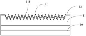
- the encapsulation layer includes an organic layer 11, a protective layer 12, a barrier layer 13 and a stress layer 14; a first curved surface region 111 is formed on the organic layer 11.
- the protective layer 12, the barrier layer 13 and the stress layer 14 are sequentially laminated on the organic layer 11, and the second curved surface region is formed on the protective layer 12, the barrier layer 13 and the stress layer 14, and the second curved surface region is formed.
- the first curved surface area 11 is stacked and overlapped, and the second curved surface area is laminated with the first curved surface area 11 to form a folded area 15 of the OLED device. It is to be noted that the second curved surface region and the first curved surface region 11 are projected on the OLED body 10 to overlap each other, and are stacked to form a regular folded region 15.
- the encapsulation layer is provided in a plurality of layers and laminated, and each two adjacent encapsulation layers are adhered to the stress layer through the organic layer, that is, the alternate layer arrangement of the organic layer and the inorganic layer of different layers may be set according to different requirements. .
- the encapsulation layer is one.
- the OLED body 10 includes a cathode layer 101.
- the encapsulation layer is attached to the cathode layer 101.
- a barrier protection layer 16 is disposed between the cathode layer 10 and the organic layer 11.
- the first curved surface region of the organic layer 11 is formed by a plurality of regular pyramids or a plurality of regular grooves arranged in a matrix.
- the first curved surface region is formed by stamping a mold.
- the cone is a four-sided cone or a cone; the groove has a triangular or curved cross section.
- the four-sided cone or the tapered or triangular groove or the curved groove is disposed on the surface of the imprinting mold, and the film is embossed to form a corresponding curved surface region. Referring to FIG.
- the surface of the mold is convexly provided with a plurality of embossed surfaces which are arranged in a matrix at intervals, and the mold embossed organic layer 11 forms a first curved surface region.
- the protective layer 12, the barrier layer 13, and the stress layer 14 are laminated to the organic layer 11, a second curved surface region is formed at a position corresponding to the first curved surface region.
- the protective layer 12 is made of a transparent metal, including but not limited to an inorganic material such as Al, Ag, or the like which is a transparent metal at a certain thickness to protect the organic layer 11.
- the barrier layer 13 is made of an inorganic material, and is deposited on the protective layer by using, but not limited to, a PECVD (Plasma Enhanced Chemical Vapor Deposition)-plasma enhanced chemical vapor deposition method, including but not limited to Al 2 O 3 , An inorganic material such as SiN x , TiO 2 or SiO x forms the barrier layer.
- PECVD Pullasma Enhanced Chemical Vapor Deposition
- Al 2 O 3 Al 2 O 3
- An inorganic material such as SiN x , TiO 2 or SiO x forms the barrier layer.
- the stress layer 14 is made of a polymer material, and deposition on the barrier layer includes, but not limited to, HMDSO (hexamethyldimethicone) polymer pp-HMDSO (Plasma Polymerized HMDSO), polyacrylate, poly Transparent polymers such as carbonates and polystyrenes form stress layers to alleviate the stress of the barrier layer during folding and crimping.
- HMDSO hexamethyldimethicone
- pp-HMDSO Polyacrylate
- Poly Transparent polymers such as carbonates and polystyrenes form stress layers to alleviate the stress of the barrier layer during folding and crimping.
- an inorganic layer 17 is further laminated on the stress layer 14.
- the encapsulation film of different organic layer and inorganic layer alternately is deposited on the body 10 according to actual needs to achieve effective barrier to water oxygen and effective extension of folding and curling life.
- the barrier layer may be the same as or different from the inorganic layer material.
- the folding area 15 is one, see FIG. 2. It will be appreciated that the folded regions 15 may be arranged in multiple and spaced apart intervals. The case where the OLED device is folded a plurality of times when the folded region 15 is plural is suitable for the curling or being flexible of the OLED device when the folded region 15 extends over the entire display region.
- the encapsulation layer is fabricated.
- step 1 the mold 20 and the OLED body 10 provided with the organic layer 11 are provided.
- the surface of the mold 20 is convexly disposed with a plurality of embossed surfaces 21 arranged in a matrix at four intervals.
- step two imprinting the organic layer 11 by the embossed surface 21 of the mold 20, in organic
- the surface of layer 11 is embossed into a first curved surface region 111 (Fig. 4).
- the protective layer 12 is formed on the surface of the organic layer 11 by vacuum evaporation of the transparent metal, and the second curved surface region 121 is formed on the protective layer 12 corresponding to the first curved surface region 111 (FIG. 5).
- Step 4 forming a barrier layer 13 on the protective layer 12 by deposition, and forming a second curved surface region 131 on the barrier layer 13 corresponding to the first curved surface region 111 (FIG. 6).
- step 5 the stress layer 14 is formed on the barrier layer 13 by deposition, and the second curved surface region 141 is formed on the stress layer 14 corresponding to the first curved surface region 111 (FIG. 1).
- the OLED device package structure described in the present application is stacked with an alternating inorganic film and an organic film, and the organic layer 11 and the stress layer 14 having a curved surface region can more effectively alleviate the folding of the flexible OLED device.
- the stress generated during curling, while the protective layer 12 and the barrier layer 13 having the curved surface region can effectively extend the penetration path of water oxygen in the film encapsulation layer, thereby achieving good folding and curling effects, and prolonging the operation of the flexible OLED element. life.
- the special shape folding area 15 is formed by embossing by a mold process, which is simple in process and low in cost.
- the present application also provides a flexible display screen having an OLED device including the OLED device package structure described in the above embodiments.
- the OLED device adopts the above package structure, which can increase the flexibility and bending life of the flexible display.
Landscapes
- Physics & Mathematics (AREA)
- Optics & Photonics (AREA)
- Engineering & Computer Science (AREA)
- Manufacturing & Machinery (AREA)
- Chemical & Material Sciences (AREA)
- Inorganic Chemistry (AREA)
- Electroluminescent Light Sources (AREA)
- Devices For Indicating Variable Information By Combining Individual Elements (AREA)
Abstract
Description
本发明要求2016年5月17日递交的发明名称为“OLED器件封装结构、OLED器件及显示屏”的申请号201610325919.7的在先申请优先权,上述在先申请的内容以引入的方式并入本文本中。The present invention claims the priority of the prior application entitled " OLED device package structure, OLED device and display screen" filed on May 17, 2016, the content of which is hereby incorporated by reference. This.
本发明涉及液晶显示技术领域,特别涉及一种OLED器件封装结构、OLED器件及显示屏。The present invention relates to the field of liquid crystal display technologies, and in particular, to an OLED device package structure, an OLED device, and a display screen.
随着显示技术的发展,新一代显示技术的开发与应用化进行得如火如荼并且逐渐被应用到多个领域,可穿戴设备如智能手环、智能手表、VR(Virtual Reality,即虚拟现实)设备,移动电话机,电子书和电子报纸,电视机,个人便携电脑等。With the development of display technology, the development and application of a new generation of display technology is in full swing and is gradually applied to many fields, such as smart bracelets, smart watches, VR (Virtual Reality) devices, Mobile phones, e-books and electronic newspapers, televisions, personal laptops, etc.
有机发光二极管又称为有机电激光显示(Organic Light-Emitting Diode,OLED)本身的操作使用寿命是研发OLED极其重要的课题之一,OLED元件对水氧极度敏感的元件,特别是对水气,如果元件没有封装,很容易在发光区域形成黑点,并且黑点会随着时间而扩大。目前广泛采用的封装方式是玻璃盖板封装的方式,但是对于OLED即可折叠OLED和卷曲OLED而言,薄膜封装(Thin Film Encapsulation)是最适合的方法之一。目前薄膜封装采用最普遍的技术就是聚合物有机薄膜和无机薄膜交替沉积在OLED表面,无机薄膜具有良好的水氧阻隔性,聚合物薄膜可以很好的吸收与分散层与层之间的应力,避免致密的无机薄膜产生裂痕而降低对水氧的阻隔性。对于可折叠OLED和卷曲OLED而言,普通平面的聚合物薄膜和无机薄膜交替沉积还是无法做到足够的折叠寿命次数以及更小的卷曲曲率。Organic light-emitting diodes (OLEDs), also known as organic light-emitting diodes (OLEDs), have an operational lifetime that is one of the most important topics in the development of OLEDs. OLED components are extremely sensitive to water and oxygen, especially to water vapor. If the component is not packaged, it is easy to form a black dot in the light-emitting area, and the black dot will expand with time. The currently widely used packaging method is a glass cover package, but for OLED foldable OLEDs and crimped OLEDs, Thin Film Encapsulation is one of the most suitable methods. At present, the most common technology for film encapsulation is that polymer organic film and inorganic film are alternately deposited on the surface of OLED. The inorganic film has good water and oxygen barrier properties, and the polymer film can absorb and disperse the stress between the layer and the layer. Avoid cracking of dense inorganic film and reduce barrier to water and oxygen. For collapsible OLEDs and crimped OLEDs, alternating flat polymer film and inorganic film are not able to achieve sufficient folding life and smaller curl curvature.
发明内容Summary of the invention
本发明的目的在于提供一种OLED器件,增强所述OLED器件的柔韧度, 提高折叠寿命。It is an object of the present invention to provide an OLED device that enhances the flexibility of the OLED device, Improve folding life.
所述OLED器件包括OLED本体及封装层,其中,所述封装层包括有机层、保护层、阻隔层及应力层;所述有机层上形成有第一曲面区域,所述保护层、阻隔层及应力层依次层叠于所述有机层上,所述保护层、阻隔层及应力层上均形成第二曲面区域,所述第二曲面区域与所述第一曲面区域层叠设置并重合,所述第二曲面区域与所述第一曲面区域形成封装层的折叠区域。The OLED device includes an OLED body and an encapsulation layer, wherein the encapsulation layer includes an organic layer, a protective layer, a barrier layer and a stress layer; the organic layer is formed with a first curved surface region, the protective layer and the barrier layer and a stress layer is sequentially stacked on the organic layer, and a second curved surface region is formed on the protective layer, the barrier layer and the stress layer, and the second curved surface region is stacked and overlapped with the first curved surface region, The two curved surface regions and the first curved surface region form a folded region of the encapsulation layer.
其中,所述第一曲面区域由多个规则锥体,或者多个规则沟槽呈矩阵式间隔排列形成。The first curved surface area is formed by a plurality of regular cones or a plurality of regular grooves arranged in a matrix.
其中,所述封装层为多个且层叠设置,并且每两个相邻的封装层通过有机层与应力层贴合。具体的,在压印模具表面设置所述四面锥或者圆锥或者三角形沟槽或者弧形沟槽,对薄膜进行压印形成相应的曲面区域。Wherein, the encapsulation layer is plural and laminated, and each two adjacent encapsulation layers are bonded to the stress layer through an organic layer. Specifically, the four-sided cone or the tapered or triangular groove or the curved groove is disposed on the surface of the imprinting mold, and the film is embossed to form a corresponding curved surface region.
其中,所述OLED本体包括阴极层,所述阴极层与所述有机层之间设有阻隔保护层。Wherein, the OLED body comprises a cathode layer, and a barrier protective layer is disposed between the cathode layer and the organic layer.
其中,所述保护层为透明金属通过真空蒸镀形成于所述有机层上,所述保护层包括但不限于Al、Ag等在一定厚度下为透明金属的无机材料,用以保护所述有机层。Wherein the protective layer is a transparent metal formed on the organic layer by vacuum evaporation, and the protective layer includes, but is not limited to, an inorganic material such as Al, Ag or the like which is a transparent metal at a certain thickness to protect the organic layer. Floor.
其中,所述阻隔层为无机材料通过沉积方式形成于所述保护层上。Wherein, the barrier layer is formed on the protective layer by deposition of an inorganic material.
其中,所述应力层为聚合物材料制成。Wherein, the stress layer is made of a polymer material.
其中,所述应力层上还层叠有无机层。根据实际需要来沉积不同的有机层和无机层交替结构薄膜来实现对水氧的有效阻隔和对折叠和卷曲寿命的有效延长。阻隔层与与无机层材料可以相同或者不同。Wherein, the inorganic layer is further laminated on the stress layer. Different organic and inorganic layer alternating structure films are deposited according to actual needs to achieve effective barrier to water and oxygen and effective extension of folding and crimping life. The barrier layer may be the same as or different from the inorganic layer material.
其中,所述折叠区域为一个,或者多个且间隔设置。当折叠区域为多个时适合OLED器件折叠多次的情况。The folding area is one, or multiple, and spaced apart. It is suitable for the case where the OLED device is folded a plurality of times when the folding area is plural.
本申请提供一种OLED器件,其包括所述的OLED器件封装结构。The application provides an OLED device including the OLED device package structure.
本申请提供一种显示屏,其包括所述的OLED器件。The application provides a display screen comprising the OLED device.
本发明所述OLED器件封装结构具有曲面区域组成的弯折区域,实现良好的折叠和卷曲效果,同时延长柔性OLED器件的操作寿命。The OLED device package structure of the present invention has a bent region composed of curved regions, achieving good folding and curling effects, and prolonging the operational life of the flexible OLED device.
为了更清楚地说明本发明实施例或现有技术中的技术方案,下面将对实施例或现有技术描述中所需要使用的附图作简单地介绍,显而易见地,下面描述中的附图仅仅是本发明的一些实施例,对于本领域普通技术人员来讲,在不付出创造性劳动的前提下,还可以根据这些附图获得其他的附图。In order to more clearly illustrate the embodiments of the present invention or the technical solutions in the prior art, the drawings used in the embodiments or the description of the prior art will be briefly described below. Obviously, the drawings in the following description are only It is a certain embodiment of the present invention, and other drawings can be obtained from those skilled in the art without any creative work.
图1是本发明的OLED器件封装结构的示意图。1 is a schematic view of a package structure of an OLED device of the present invention.
图2是具有图1所述的OLED器件的显示屏的示意图。2 is a schematic illustration of a display screen having the OLED device of FIG.
图3是制造图1的OLED器件封装结构的有机层的第一曲面区域的模具示意图。3 is a schematic view of a mold for fabricating a first curved surface region of an organic layer of the OLED device package structure of FIG. 1.
图4-图6是图1所述的OLED器件封装结构步骤图。4-6 are step diagrams of the OLED device package structure illustrated in FIG. 1.
下面将结合本发明实施例中的附图,对本发明实施例中的技术方案进行清楚、完整地描述,显然,所描述的实施例仅仅是本发明一部分实施例,而不是全部的实施例。基于本发明中的实施例,本领域普通技术人员在没有作出创造性劳动前提下所获得的所有其他实施例,都属于本发明保护的范围。The technical solutions in the embodiments of the present invention are clearly and completely described in the following with reference to the accompanying drawings in the embodiments of the present invention. It is obvious that the described embodiments are only a part of the embodiments of the present invention, but not all embodiments. All other embodiments obtained by those skilled in the art based on the embodiments of the present invention without creative efforts are within the scope of the present invention.
请参阅图1与图2,本发明佳实施方式提供所述OLED器件封装结构用于OLED器件上,特别是柔性的OLED器件。所述OLED器件包括OLED本体10及封装层(图未标)。所述封装层包括有机层11、保护层12、阻隔层13及应力层14;所述有机层11上形成有第一曲面区域111。所述保护层12、阻隔层13及应力层14依次层叠于所述有机层11上,所述保护层12、阻隔层13及应力层14上均形成第二曲面区域,所述第二曲面区域与所述第一曲面区域11层叠设置并重合,所述第二曲面区域与所述第一曲面区域11层叠设置形成OLED器件的折叠区域15。需要说明书的是,所述第二曲面区域与所述第一曲面区域11在OLED本体10上投影重合,层叠后构成规则的折叠区域15。Referring to FIG. 1 and FIG. 2, a preferred embodiment of the present invention provides the OLED device package structure for use in an OLED device, particularly a flexible OLED device. The OLED device includes an
所述封装层为多个且层叠设置,并且每两个相邻的封装层通过有机层与应力层贴合,也就是说根据不同需求,可以设置不同层的有机层与无机层的交替层叠设置。本实施例中,所述封装层为一个。所述OLED本体10包括阴极层101,所述封装层贴于所述阴极层101上,所述阴极层10与所述有机层11之间设有阻隔保护层16。
The encapsulation layer is provided in a plurality of layers and laminated, and each two adjacent encapsulation layers are adhered to the stress layer through the organic layer, that is, the alternate layer arrangement of the organic layer and the inorganic layer of different layers may be set according to different requirements. . In this embodiment, the encapsulation layer is one. The
进一步的,所述有机层11的第一曲面区域均由多个规则锥体,或者多个规则沟槽呈矩阵式间隔排列形成。其中,所述第一曲面区域为模具压印形成。其中,所述锥体为四面锥或者圆锥;所述沟槽的截面呈三角形或者弧形。具体的,在压印模具表面设置所述四面锥或者圆锥或者三角形沟槽或者弧形沟槽,对薄膜进行压印形成相应的曲面区域。参阅图2,模具表面凸设置数个呈矩阵间隔排列四面锥构成的压印面,模具压印有机层11形成第一曲面区域。保护层12、阻隔层13及应力层14在层叠到有机层11时,在对应所述第一曲面区域的位置均形成第二曲面区域。Further, the first curved surface region of the
其中,所述保护层12为透明金属制成,包括但不限于Al、Ag等在一定厚度下为透明金属的无机材料,用以保护所述有机层11。The
其中,所述阻隔层13为无机材料制成,利用包括但不限于PECVD(Plasma Enhanced Chemical Vapor Deposition)--等离子体增强化学气相沉积法方法在保护层上沉积包括但不限于Al2O3、SiNx、TiO2、SiOx等无机材料形成所述阻隔层。Wherein, the
其中,所述应力层14为聚合物材料制成,在阻隔层上沉积包括但不限于HMDSO(六甲基二甲硅醚)聚合体pp-HMDSO(Plasma Polymerized HMDSO)、聚丙烯酸酯类、聚碳酸脂类、聚苯乙烯类等透明聚合物形成应力层来缓解阻隔层在折叠和卷曲过程中的应力。Wherein, the
进一步的,所述应力层14上还层叠有无机层17。根据实际需要在本体10上来沉积不同的有机层和无机层交替结构的封装层薄膜来实现对水氧的有效阻隔和对折叠和卷曲寿命的有效延长。阻隔层与与无机层材料可以相同或者不同。Further, an inorganic layer 17 is further laminated on the
其中,所述折叠区域15为一个,参阅图2。可以理解,所述折叠区域15可以为多个且平行间隔设置。当折叠区域15为多个时适合OLED器件折叠多次的情况,当折叠区域15延伸到整个显示区域时适合OLED器件的卷曲或者可挠的情况。Wherein, the
请参阅图3,制造所述封装层,步骤一,提供所述模具20以及设有有机层11的OLED本体10,模具20表面凸设置数个呈矩阵间隔排列四面锥构成的压印面21。步骤二,通过模具20的压印面21压印所述有机层11,在有机
层11表面上压印成第一曲面区域111(图4)。步骤三通过真空蒸镀透明金属在有机层11表面形成保护层12,同时保护层12上对应所述第一曲面区域111位置形成第二曲面区域121(图5)。步骤四,在所述保护层12上通过沉积方式形成阻隔层13,同时阻隔层13上对应所述第一曲面区域111位置形成第二曲面区域131(图6)。步骤五,在所述阻隔层13上通过沉积方式形成应力层14,同时应力层14上对应所述第一曲面区域111位置形成第二曲面区域141(图1)。Referring to FIG. 3, the encapsulation layer is fabricated. In step 1, the
本申请所述的OLED器件封装结构相对于普通平面的薄膜封装,采用交替的无机薄膜和有机薄膜层叠设置,具有曲面区域的有机层11及应力层14可以更有效地缓解柔性OLED器件在折叠和卷曲时候产生的应力,同时具有曲面区域的保护层12、阻隔层13能够有效地延长了水氧在薄膜封装层中的渗透路径,从而实现良好的折叠和卷曲效果,同时延长柔性OLED元件的操作寿命。而且通过模具工艺压印形成特殊形状折叠区域15,制程简单,成本低。The OLED device package structure described in the present application is stacked with an alternating inorganic film and an organic film, and the
本申请还提供一种有OLED器件的柔性显示屏,所述OLED器件包括以上实施例所述的OLED器件封装结构。OLED器件采用上述封装结构,可以增加,柔性显示屏柔韧度及弯曲寿命。The present application also provides a flexible display screen having an OLED device including the OLED device package structure described in the above embodiments. The OLED device adopts the above package structure, which can increase the flexibility and bending life of the flexible display.
以上所揭露的仅为本发明较佳实施例而已,当然不能以此来限定本发明之权利范围,本领域普通技术人员可以理解实现上述实施例的全部或部分流程,并依本发明权利要求所作的等同变化,仍属于发明所涵盖的范围。 The above is only the preferred embodiment of the present invention, and the scope of the present invention is not limited thereto, and those skilled in the art can understand all or part of the process of implementing the above embodiments, and according to the claims of the present invention. The equivalent change is still within the scope of the invention.
Claims (17)
Priority Applications (3)
| Application Number | Priority Date | Filing Date | Title |
|---|---|---|---|
| KR1020187036639A KR102177624B1 (en) | 2016-05-17 | 2016-06-20 | OLED device encapsulation structure, OLED device and display screen |
| JP2018560109A JP6709298B2 (en) | 2016-05-17 | 2016-06-20 | Package structure of OLED device, OLED device and display screen |
| US15/111,008 US10115929B2 (en) | 2016-05-17 | 2016-06-20 | OLED device encapsulation structures, OLED devices, and display panels |
Applications Claiming Priority (2)
| Application Number | Priority Date | Filing Date | Title |
|---|---|---|---|
| CN201610325919.7A CN105810845B (en) | 2016-05-17 | 2016-05-17 | OLED device packaging structure, OLED device and display screen |
| CN201610325919.7 | 2016-05-17 |
Publications (1)
| Publication Number | Publication Date |
|---|---|
| WO2017197699A1 true WO2017197699A1 (en) | 2017-11-23 |
Family
ID=56452324
Family Applications (1)
| Application Number | Title | Priority Date | Filing Date |
|---|---|---|---|
| PCT/CN2016/086346 Ceased WO2017197699A1 (en) | 2016-05-17 | 2016-06-20 | Oled device encapsulation structure, oled device and display screen |
Country Status (5)
| Country | Link |
|---|---|
| US (1) | US10115929B2 (en) |
| JP (1) | JP6709298B2 (en) |
| KR (1) | KR102177624B1 (en) |
| CN (1) | CN105810845B (en) |
| WO (1) | WO2017197699A1 (en) |
Families Citing this family (15)
| Publication number | Priority date | Publication date | Assignee | Title |
|---|---|---|---|---|
| CN106450036B (en) * | 2016-11-24 | 2019-01-22 | 武汉华星光电技术有限公司 | OLED encapsulating structure, OLED device and display screen |
| CN106783881A (en) * | 2016-12-26 | 2017-05-31 | 武汉华星光电技术有限公司 | A kind of flexible display panels and its manufacture method |
| CN109004099B (en) * | 2017-06-07 | 2021-06-22 | 上海和辉光电有限公司 | Flexible display panel and preparation method thereof |
| CN109309169A (en) * | 2017-07-26 | 2019-02-05 | 上海和辉光电有限公司 | A kind of organic light emitting display panel and preparation method thereof |
| CN109427248A (en) * | 2017-08-28 | 2019-03-05 | 霸州市云谷电子科技有限公司 | A kind of flexible display panels and preparation method thereof, display device |
| CN108878680A (en) * | 2018-06-26 | 2018-11-23 | 武汉华星光电半导体显示技术有限公司 | A kind of encapsulation type display device and display panel |
| CN108598289B (en) * | 2018-07-12 | 2019-11-08 | 京东方科技集团股份有限公司 | Package cover plate and its manufacturing method, display panel and display device |
| CN208753371U (en) * | 2018-11-02 | 2019-04-16 | 京东方科技集团股份有限公司 | Flexible display panels and display device |
| CN111146361B (en) * | 2019-12-30 | 2023-09-29 | 固安翌光科技有限公司 | Film packaging structure and organic photoelectric device |
| US11151366B2 (en) * | 2020-01-30 | 2021-10-19 | Toyota Motor Engineering & Manufacturing North America, Inc. | Systems and methods for occluding vehicle occupant communication |
| CN115210900B (en) * | 2020-02-28 | 2025-05-06 | 应用材料公司 | Treatments for improved thin film encapsulation |
| CN111833740B (en) | 2020-06-16 | 2022-08-19 | 京东方科技集团股份有限公司 | Flexible display device |
| CN112820844A (en) * | 2021-01-27 | 2021-05-18 | 福州大学 | Thin film packaging structure and preparation method thereof |
| CN113130470B (en) * | 2021-04-21 | 2022-08-16 | 深圳市芯视佳半导体科技有限公司 | Micro-display structure and manufacturing method thereof |
| KR102716703B1 (en) | 2021-10-20 | 2024-10-15 | 한국전자통신연구원 | Encapsulation material for light emitting devices and a light emitting device manufactured using the encapsulation material |
Citations (5)
| Publication number | Priority date | Publication date | Assignee | Title |
|---|---|---|---|---|
| CN102593148A (en) * | 2011-01-04 | 2012-07-18 | 三星移动显示器株式会社 | Flat panel display apparatus and organic light-emitting display apparatus |
| US20120256202A1 (en) * | 2011-04-11 | 2012-10-11 | So-Young Lee | Organic light emitting diode display and manufacturing method thereof |
| CN103811668A (en) * | 2012-11-07 | 2014-05-21 | 海洋王照明科技股份有限公司 | Organic electroluminescent device and method for producing same |
| CN104538425A (en) * | 2014-12-19 | 2015-04-22 | 上海天马微电子有限公司 | Barrier film, manufacturing method thereof and display device |
| CN105206763A (en) * | 2015-10-21 | 2015-12-30 | 京东方科技集团股份有限公司 | Flexible displayer and production method thereof |
Family Cites Families (10)
| Publication number | Priority date | Publication date | Assignee | Title |
|---|---|---|---|---|
| WO2006109526A1 (en) * | 2005-03-30 | 2006-10-19 | Pioneer Corporation | Organic el display device, organic transistor and methods for manufacturing such organic el display device and organic transistor |
| CN101412300A (en) * | 2007-10-16 | 2009-04-22 | 富士胶片株式会社 | Barrier laminate, barrier film substrate, device, and method for producing barrier laminate |
| FR2933538B1 (en) * | 2008-07-07 | 2012-09-21 | Commissariat Energie Atomique | DISPLAY, LIGHTING OR SIGNALING ELECTROLUMINESCENT DEVICE AND METHOD FOR MANUFACTURING THE SAME |
| KR101202353B1 (en) * | 2009-12-31 | 2012-11-16 | 삼성디스플레이 주식회사 | Barrier film composites, display apparatus comprising the same, manufacturing method of the barrier film composites, and manufacturing method of display apparatus comprising the same |
| TWI492436B (en) * | 2012-11-16 | 2015-07-11 | Au Optronics Corp | Flexible display panel |
| KR101453880B1 (en) * | 2012-11-29 | 2014-10-22 | 삼성디스플레이 주식회사 | Organic light emitting display apparatus and the method for manufacturing the same |
| KR101990555B1 (en) * | 2012-12-24 | 2019-06-19 | 삼성디스플레이 주식회사 | Thin film encapsulation manufacturing device and manufacturing method of thin film encapsulation |
| JP2015169711A (en) * | 2014-03-05 | 2015-09-28 | 株式会社ジャパンディスプレイ | Display device and manufacturing method thereof |
| US10388904B2 (en) * | 2014-11-07 | 2019-08-20 | Sharp Kabushiki Kaisha | Organic el display device and method for producing organic el display device |
| CN105552246A (en) * | 2015-12-07 | 2016-05-04 | 上海天马微电子有限公司 | Flexible display device and manufacturing method thereof |
-
2016
- 2016-05-17 CN CN201610325919.7A patent/CN105810845B/en active Active
- 2016-06-20 KR KR1020187036639A patent/KR102177624B1/en active Active
- 2016-06-20 US US15/111,008 patent/US10115929B2/en active Active
- 2016-06-20 JP JP2018560109A patent/JP6709298B2/en active Active
- 2016-06-20 WO PCT/CN2016/086346 patent/WO2017197699A1/en not_active Ceased
Patent Citations (5)
| Publication number | Priority date | Publication date | Assignee | Title |
|---|---|---|---|---|
| CN102593148A (en) * | 2011-01-04 | 2012-07-18 | 三星移动显示器株式会社 | Flat panel display apparatus and organic light-emitting display apparatus |
| US20120256202A1 (en) * | 2011-04-11 | 2012-10-11 | So-Young Lee | Organic light emitting diode display and manufacturing method thereof |
| CN103811668A (en) * | 2012-11-07 | 2014-05-21 | 海洋王照明科技股份有限公司 | Organic electroluminescent device and method for producing same |
| CN104538425A (en) * | 2014-12-19 | 2015-04-22 | 上海天马微电子有限公司 | Barrier film, manufacturing method thereof and display device |
| CN105206763A (en) * | 2015-10-21 | 2015-12-30 | 京东方科技集团股份有限公司 | Flexible displayer and production method thereof |
Also Published As
| Publication number | Publication date |
|---|---|
| CN105810845B (en) | 2018-05-25 |
| CN105810845A (en) | 2016-07-27 |
| JP6709298B2 (en) | 2020-06-10 |
| US20170373279A1 (en) | 2017-12-28 |
| US10115929B2 (en) | 2018-10-30 |
| KR20190012186A (en) | 2019-02-08 |
| JP2019517105A (en) | 2019-06-20 |
| KR102177624B1 (en) | 2020-11-11 |
Similar Documents
| Publication | Publication Date | Title |
|---|---|---|
| WO2017197699A1 (en) | Oled device encapsulation structure, oled device and display screen | |
| CN105977398B (en) | A kind of encapsulation cover plate and preparation method thereof, display device | |
| CN105261712B (en) | A kind of flexible OLED display panel | |
| CN109461832B (en) | A flexible display panel and method of making the same | |
| US10050230B1 (en) | OLED display and manufacturing method thereof | |
| US6576351B2 (en) | Barrier region for optoelectronic devices | |
| US7187119B2 (en) | Methods and structures for reducing lateral diffusion through cooperative barrier layers | |
| TWI492436B (en) | Flexible display panel | |
| US20120064278A1 (en) | Package of environmental sensitive element and encapsulation method thereof | |
| CN107425134B (en) | A kind of organic electroluminescent display panel, its production method and display device | |
| CN109256481B (en) | Display panel and display device | |
| EP3534425A1 (en) | Oled display device | |
| CN104900681A (en) | Organic light-emitting display panel and forming method thereof | |
| CN106876434B (en) | Organic light-emitting diode display panel, manufacturing method thereof and display device | |
| JP2009501426A (en) | OLED devices with improved efficiency and durability | |
| US9935289B2 (en) | Environmental sensitive element package and encapsulation method thereof | |
| KR20150031133A (en) | Method of manufacturing an organic light emitting display device | |
| KR20140043022A (en) | Organic light emitting display device and method of manufacturing the same | |
| US10396256B2 (en) | Electronic device package | |
| CN107275515B (en) | OLED device packaging method, structure, OLED device and display screen | |
| WO2017033823A1 (en) | Electronic device | |
| CN109713155B (en) | Encapsulation film, display panel and preparation method thereof | |
| CN115943750A (en) | Combined thin film encapsulation in flexible display device and manufacturing method thereof | |
| CN111028709A (en) | Display module and display device | |
| CN115988909A (en) | A display panel and a display device |
Legal Events
| Date | Code | Title | Description |
|---|---|---|---|
| WWE | Wipo information: entry into national phase |
Ref document number: 15111008 Country of ref document: US |
|
| ENP | Entry into the national phase |
Ref document number: 2018560109 Country of ref document: JP Kind code of ref document: A |
|
| NENP | Non-entry into the national phase |
Ref country code: DE |
|
| 121 | Ep: the epo has been informed by wipo that ep was designated in this application |
Ref document number: 16902081 Country of ref document: EP Kind code of ref document: A1 |
|
| ENP | Entry into the national phase |
Ref document number: 20187036639 Country of ref document: KR Kind code of ref document: A |
|
| 122 | Ep: pct application non-entry in european phase |
Ref document number: 16902081 Country of ref document: EP Kind code of ref document: A1 |