WO2016141705A1 - Array substrate and manufacturing method thereof, and display device - Google Patents
Array substrate and manufacturing method thereof, and display device Download PDFInfo
- Publication number
- WO2016141705A1 WO2016141705A1 PCT/CN2015/089834 CN2015089834W WO2016141705A1 WO 2016141705 A1 WO2016141705 A1 WO 2016141705A1 CN 2015089834 W CN2015089834 W CN 2015089834W WO 2016141705 A1 WO2016141705 A1 WO 2016141705A1
- Authority
- WO
- WIPO (PCT)
- Prior art keywords
- gate
- array substrate
- extending direction
- data line
- thin film
- Prior art date
- Legal status (The legal status is an assumption and is not a legal conclusion. Google has not performed a legal analysis and makes no representation as to the accuracy of the status listed.)
- Ceased
Links
Images


Classifications
-
- G—PHYSICS
- G02—OPTICS
- G02F—OPTICAL DEVICES OR ARRANGEMENTS FOR THE CONTROL OF LIGHT BY MODIFICATION OF THE OPTICAL PROPERTIES OF THE MEDIA OF THE ELEMENTS INVOLVED THEREIN; NON-LINEAR OPTICS; FREQUENCY-CHANGING OF LIGHT; OPTICAL LOGIC ELEMENTS; OPTICAL ANALOGUE/DIGITAL CONVERTERS
- G02F1/00—Devices or arrangements for the control of the intensity, colour, phase, polarisation or direction of light arriving from an independent light source, e.g. switching, gating or modulating; Non-linear optics
- G02F1/01—Devices or arrangements for the control of the intensity, colour, phase, polarisation or direction of light arriving from an independent light source, e.g. switching, gating or modulating; Non-linear optics for the control of the intensity, phase, polarisation or colour
- G02F1/13—Devices or arrangements for the control of the intensity, colour, phase, polarisation or direction of light arriving from an independent light source, e.g. switching, gating or modulating; Non-linear optics for the control of the intensity, phase, polarisation or colour based on liquid crystals, e.g. single liquid crystal display cells
- G02F1/133—Constructional arrangements; Operation of liquid crystal cells; Circuit arrangements
- G02F1/136—Liquid crystal cells structurally associated with a semi-conducting layer or substrate, e.g. cells forming part of an integrated circuit
- G02F1/1362—Active matrix addressed cells
- G02F1/136286—Wiring, e.g. gate line, drain line
-
- G—PHYSICS
- G02—OPTICS
- G02F—OPTICAL DEVICES OR ARRANGEMENTS FOR THE CONTROL OF LIGHT BY MODIFICATION OF THE OPTICAL PROPERTIES OF THE MEDIA OF THE ELEMENTS INVOLVED THEREIN; NON-LINEAR OPTICS; FREQUENCY-CHANGING OF LIGHT; OPTICAL LOGIC ELEMENTS; OPTICAL ANALOGUE/DIGITAL CONVERTERS
- G02F1/00—Devices or arrangements for the control of the intensity, colour, phase, polarisation or direction of light arriving from an independent light source, e.g. switching, gating or modulating; Non-linear optics
- G02F1/01—Devices or arrangements for the control of the intensity, colour, phase, polarisation or direction of light arriving from an independent light source, e.g. switching, gating or modulating; Non-linear optics for the control of the intensity, phase, polarisation or colour
- G02F1/13—Devices or arrangements for the control of the intensity, colour, phase, polarisation or direction of light arriving from an independent light source, e.g. switching, gating or modulating; Non-linear optics for the control of the intensity, phase, polarisation or colour based on liquid crystals, e.g. single liquid crystal display cells
- G02F1/133—Constructional arrangements; Operation of liquid crystal cells; Circuit arrangements
- G02F1/1333—Constructional arrangements; Manufacturing methods
- G02F1/1343—Electrodes
- G02F1/134309—Electrodes characterised by their geometrical arrangement
- G02F1/134363—Electrodes characterised by their geometrical arrangement for applying an electric field parallel to the substrate, i.e. in-plane switching [IPS]
-
- G—PHYSICS
- G02—OPTICS
- G02F—OPTICAL DEVICES OR ARRANGEMENTS FOR THE CONTROL OF LIGHT BY MODIFICATION OF THE OPTICAL PROPERTIES OF THE MEDIA OF THE ELEMENTS INVOLVED THEREIN; NON-LINEAR OPTICS; FREQUENCY-CHANGING OF LIGHT; OPTICAL LOGIC ELEMENTS; OPTICAL ANALOGUE/DIGITAL CONVERTERS
- G02F1/00—Devices or arrangements for the control of the intensity, colour, phase, polarisation or direction of light arriving from an independent light source, e.g. switching, gating or modulating; Non-linear optics
- G02F1/01—Devices or arrangements for the control of the intensity, colour, phase, polarisation or direction of light arriving from an independent light source, e.g. switching, gating or modulating; Non-linear optics for the control of the intensity, phase, polarisation or colour
- G02F1/13—Devices or arrangements for the control of the intensity, colour, phase, polarisation or direction of light arriving from an independent light source, e.g. switching, gating or modulating; Non-linear optics for the control of the intensity, phase, polarisation or colour based on liquid crystals, e.g. single liquid crystal display cells
- G02F1/133—Constructional arrangements; Operation of liquid crystal cells; Circuit arrangements
- G02F1/136—Liquid crystal cells structurally associated with a semi-conducting layer or substrate, e.g. cells forming part of an integrated circuit
- G02F1/1362—Active matrix addressed cells
- G02F1/1368—Active matrix addressed cells in which the switching element is a three-electrode device
-
- H—ELECTRICITY
- H10—SEMICONDUCTOR DEVICES; ELECTRIC SOLID-STATE DEVICES NOT OTHERWISE PROVIDED FOR
- H10D—INORGANIC ELECTRIC SEMICONDUCTOR DEVICES
- H10D30/00—Field-effect transistors [FET]
- H10D30/60—Insulated-gate field-effect transistors [IGFET]
- H10D30/67—Thin-film transistors [TFT]
- H10D30/6729—Thin-film transistors [TFT] characterised by the electrodes
-
- H—ELECTRICITY
- H10—SEMICONDUCTOR DEVICES; ELECTRIC SOLID-STATE DEVICES NOT OTHERWISE PROVIDED FOR
- H10D—INORGANIC ELECTRIC SEMICONDUCTOR DEVICES
- H10D86/00—Integrated devices formed in or on insulating or conducting substrates, e.g. formed in silicon-on-insulator [SOI] substrates or on stainless steel or glass substrates
- H10D86/40—Integrated devices formed in or on insulating or conducting substrates, e.g. formed in silicon-on-insulator [SOI] substrates or on stainless steel or glass substrates characterised by multiple TFTs
- H10D86/441—Interconnections, e.g. scanning lines
-
- H—ELECTRICITY
- H10—SEMICONDUCTOR DEVICES; ELECTRIC SOLID-STATE DEVICES NOT OTHERWISE PROVIDED FOR
- H10D—INORGANIC ELECTRIC SEMICONDUCTOR DEVICES
- H10D86/00—Integrated devices formed in or on insulating or conducting substrates, e.g. formed in silicon-on-insulator [SOI] substrates or on stainless steel or glass substrates
- H10D86/40—Integrated devices formed in or on insulating or conducting substrates, e.g. formed in silicon-on-insulator [SOI] substrates or on stainless steel or glass substrates characterised by multiple TFTs
- H10D86/60—Integrated devices formed in or on insulating or conducting substrates, e.g. formed in silicon-on-insulator [SOI] substrates or on stainless steel or glass substrates characterised by multiple TFTs wherein the TFTs are in active matrices
-
- G—PHYSICS
- G02—OPTICS
- G02F—OPTICAL DEVICES OR ARRANGEMENTS FOR THE CONTROL OF LIGHT BY MODIFICATION OF THE OPTICAL PROPERTIES OF THE MEDIA OF THE ELEMENTS INVOLVED THEREIN; NON-LINEAR OPTICS; FREQUENCY-CHANGING OF LIGHT; OPTICAL LOGIC ELEMENTS; OPTICAL ANALOGUE/DIGITAL CONVERTERS
- G02F1/00—Devices or arrangements for the control of the intensity, colour, phase, polarisation or direction of light arriving from an independent light source, e.g. switching, gating or modulating; Non-linear optics
- G02F1/01—Devices or arrangements for the control of the intensity, colour, phase, polarisation or direction of light arriving from an independent light source, e.g. switching, gating or modulating; Non-linear optics for the control of the intensity, phase, polarisation or colour
- G02F1/13—Devices or arrangements for the control of the intensity, colour, phase, polarisation or direction of light arriving from an independent light source, e.g. switching, gating or modulating; Non-linear optics for the control of the intensity, phase, polarisation or colour based on liquid crystals, e.g. single liquid crystal display cells
- G02F1/133—Constructional arrangements; Operation of liquid crystal cells; Circuit arrangements
- G02F1/1333—Constructional arrangements; Manufacturing methods
- G02F1/1337—Surface-induced orientation of the liquid crystal molecules, e.g. by alignment layers
- G02F1/13378—Surface-induced orientation of the liquid crystal molecules, e.g. by alignment layers by treatment of the surface, e.g. embossing, rubbing or light irradiation
- G02F1/133784—Surface-induced orientation of the liquid crystal molecules, e.g. by alignment layers by treatment of the surface, e.g. embossing, rubbing or light irradiation by rubbing
-
- G—PHYSICS
- G02—OPTICS
- G02F—OPTICAL DEVICES OR ARRANGEMENTS FOR THE CONTROL OF LIGHT BY MODIFICATION OF THE OPTICAL PROPERTIES OF THE MEDIA OF THE ELEMENTS INVOLVED THEREIN; NON-LINEAR OPTICS; FREQUENCY-CHANGING OF LIGHT; OPTICAL LOGIC ELEMENTS; OPTICAL ANALOGUE/DIGITAL CONVERTERS
- G02F1/00—Devices or arrangements for the control of the intensity, colour, phase, polarisation or direction of light arriving from an independent light source, e.g. switching, gating or modulating; Non-linear optics
- G02F1/01—Devices or arrangements for the control of the intensity, colour, phase, polarisation or direction of light arriving from an independent light source, e.g. switching, gating or modulating; Non-linear optics for the control of the intensity, phase, polarisation or colour
- G02F1/13—Devices or arrangements for the control of the intensity, colour, phase, polarisation or direction of light arriving from an independent light source, e.g. switching, gating or modulating; Non-linear optics for the control of the intensity, phase, polarisation or colour based on liquid crystals, e.g. single liquid crystal display cells
- G02F1/133—Constructional arrangements; Operation of liquid crystal cells; Circuit arrangements
- G02F1/1333—Constructional arrangements; Manufacturing methods
- G02F1/1343—Electrodes
- G02F1/134309—Electrodes characterised by their geometrical arrangement
- G02F1/134318—Electrodes characterised by their geometrical arrangement having a patterned common electrode
-
- G—PHYSICS
- G02—OPTICS
- G02F—OPTICAL DEVICES OR ARRANGEMENTS FOR THE CONTROL OF LIGHT BY MODIFICATION OF THE OPTICAL PROPERTIES OF THE MEDIA OF THE ELEMENTS INVOLVED THEREIN; NON-LINEAR OPTICS; FREQUENCY-CHANGING OF LIGHT; OPTICAL LOGIC ELEMENTS; OPTICAL ANALOGUE/DIGITAL CONVERTERS
- G02F1/00—Devices or arrangements for the control of the intensity, colour, phase, polarisation or direction of light arriving from an independent light source, e.g. switching, gating or modulating; Non-linear optics
- G02F1/01—Devices or arrangements for the control of the intensity, colour, phase, polarisation or direction of light arriving from an independent light source, e.g. switching, gating or modulating; Non-linear optics for the control of the intensity, phase, polarisation or colour
- G02F1/13—Devices or arrangements for the control of the intensity, colour, phase, polarisation or direction of light arriving from an independent light source, e.g. switching, gating or modulating; Non-linear optics for the control of the intensity, phase, polarisation or colour based on liquid crystals, e.g. single liquid crystal display cells
- G02F1/133—Constructional arrangements; Operation of liquid crystal cells; Circuit arrangements
- G02F1/136—Liquid crystal cells structurally associated with a semi-conducting layer or substrate, e.g. cells forming part of an integrated circuit
- G02F1/1362—Active matrix addressed cells
- G02F1/136286—Wiring, e.g. gate line, drain line
- G02F1/136295—Materials; Compositions; Manufacture processes
-
- G—PHYSICS
- G02—OPTICS
- G02F—OPTICAL DEVICES OR ARRANGEMENTS FOR THE CONTROL OF LIGHT BY MODIFICATION OF THE OPTICAL PROPERTIES OF THE MEDIA OF THE ELEMENTS INVOLVED THEREIN; NON-LINEAR OPTICS; FREQUENCY-CHANGING OF LIGHT; OPTICAL LOGIC ELEMENTS; OPTICAL ANALOGUE/DIGITAL CONVERTERS
- G02F2201/00—Constructional arrangements not provided for in groups G02F1/00 - G02F7/00
- G02F2201/40—Arrangements for improving the aperture ratio
-
- H—ELECTRICITY
- H10—SEMICONDUCTOR DEVICES; ELECTRIC SOLID-STATE DEVICES NOT OTHERWISE PROVIDED FOR
- H10D—INORGANIC ELECTRIC SEMICONDUCTOR DEVICES
- H10D30/00—Field-effect transistors [FET]
- H10D30/60—Insulated-gate field-effect transistors [IGFET]
- H10D30/67—Thin-film transistors [TFT]
- H10D30/6729—Thin-film transistors [TFT] characterised by the electrodes
- H10D30/673—Thin-film transistors [TFT] characterised by the electrodes characterised by the shapes, relative sizes or dispositions of the gate electrodes
Definitions
- the source of the thin film transistor is the connection portion or a part of the connection portion.
- the invention also provides a method for manufacturing an array substrate, comprising the following steps:
- the angle between the extending direction of the gate line of the array substrate and the extending direction of the data line segment 30 is ⁇ , 60° ⁇ ⁇ ⁇ 87°
- the extending direction of the side of the protruding structure close to the pixel electrode The angle with the extending direction of the gate line is ⁇ , 20° ⁇ ⁇ ⁇ 70°, so that the array substrate can obtain an optimized viewing angle direction, a high aperture ratio, and a good display quality.
- the embodiment provides an array substrate including a plurality of gate lines (eg, Gi-1, Gi, Gi+1) and a plurality of data lines (eg, Dj-) disposed at intersections.
- Dj, Dj+1 and pixel cells defined by adjacent gate lines and adjacent data lines, each data line comprising a plurality of data line segments 30, each data line segment 30 corresponding to one pixel unit, and the same
- the two adjacent data line segments 30 of the data line are connected by a connecting portion 30a; the angle between the extending direction of the gate line and the extending direction of the data line segment 30 is ⁇ ; wherein 60° ⁇ ⁇ ⁇ 87°;
- the gate of the thin film transistor is a bump structure 10 of a gate line, and an angle between an extending direction of a side of the bump structure adjacent to the pixel electrode and an extending direction of the gate line is ⁇ , wherein 20° ⁇ ⁇ ⁇ 70 °.
- Step 4 on the substrate 1 that completes the above steps, depositing an active layer film of a thin film transistor by a chemical vapor deposition, plasma assisted chemical vapor deposition or sputtering, and forming an active layer of the thin film transistor by a patterning process Graphics.
- the material of the active layer 20 may be amorphous silicon, polycrystalline silicon, microcrystalline silicon or an oxide semiconductor.
- Step 7 On the substrate 1 which has completed the above steps, a transparent conductive metal oxide film is deposited by sputtering. Then, a pattern of the common electrode 60 is formed by a patterning process such that the common electrode 60 is disposed above the pixel electrode 50 and insulated from the pixel electrode 50, and the common electrode 60 has a slit, the slit The extending direction is parallel to the extending direction of the data line.
Landscapes
- Physics & Mathematics (AREA)
- Nonlinear Science (AREA)
- Mathematical Physics (AREA)
- Chemical & Material Sciences (AREA)
- Crystallography & Structural Chemistry (AREA)
- General Physics & Mathematics (AREA)
- Optics & Photonics (AREA)
- Engineering & Computer Science (AREA)
- Microelectronics & Electronic Packaging (AREA)
- Geometry (AREA)
- Liquid Crystal (AREA)
- Devices For Indicating Variable Information By Combining Individual Elements (AREA)
- Thin Film Transistor (AREA)
- Spectroscopy & Molecular Physics (AREA)
Abstract
Description
本发明属于显示技术领域,具体涉及一种阵列基板及其制造方法和显示装置。The present invention belongs to the field of display technologies, and in particular, to an array substrate, a manufacturing method thereof, and a display device.
液晶显示技术广泛应用于电视、手机以及公共信息显示。液晶显示模式可以分成扭曲向列相(TN,twisted nematic)模式,垂直取向(VA,vertical aligned)模式和水平电场(horizontal electrical field)模式。其中,水平电场模式包括面内开关(IPS,in-plane switching)模式和边缘场开关模式(FFS,Fringe field switching),除VA模式以外,TN和水平电场模式的液晶显示面板都需要摩擦工艺,以使液晶分子具有一个初始的排列方向。液晶显示面板的优化视角方向与摩擦方向有密切关系。Liquid crystal display technology is widely used in television, mobile phones and public information displays. The liquid crystal display mode can be divided into a twisted nematic (TN) mode, a vertically aligned (VA) mode, and a horizontal electric field mode. The horizontal electric field mode includes an in-plane switching (IPS) mode and a fringe field switching mode (FFS, Fringe field switching). In addition to the VA mode, the TN and the horizontal electric field mode liquid crystal display panels all require a rubbing process. So that the liquid crystal molecules have an initial alignment direction. The optimized viewing angle of the liquid crystal display panel is closely related to the rubbing direction.
对于FFS模式,液晶显示面板包括阵列基板和彩膜基板,阵列基板包括多条栅线、多条数据线和多个像素单元,栅线与数据线垂直交叉,相邻的栅线与数据线限定出像素单元,像素单元包括:薄膜晶体管、像素电极、公共电极;其中,公共电极位于像素电极上方,且公共电极上形成有狭缝,像素电极和公共电极之间设置有绝缘层,数据线上的数据电压通过薄膜晶体管写入像素电极,整块公共电极覆盖所有的像素单元。FFS模式的液晶显示面板需要摩擦工艺,使液晶分子具有一个初始的排列方向,现有技术中FFS的摩擦取向的方向与数据线的延伸方向具有大约7°的夹角,而由于数据线和栅线是垂直交叉设置的,因此在沿数据线的延伸方向观看显示面板,并不能得到一个优化的视角方向。For the FFS mode, the liquid crystal display panel includes an array substrate and a color filter substrate. The array substrate includes a plurality of gate lines, a plurality of data lines, and a plurality of pixel units. The gate lines and the data lines vertically intersect, and adjacent gate lines and data lines are defined. a pixel unit, the pixel unit includes: a thin film transistor, a pixel electrode, and a common electrode; wherein the common electrode is located above the pixel electrode, and a slit is formed on the common electrode, and an insulating layer is disposed between the pixel electrode and the common electrode, and the data line is disposed The data voltage is written to the pixel electrode through the thin film transistor, and the entire common electrode covers all the pixel units. The liquid crystal display panel of the FFS mode requires a rubbing process to make the liquid crystal molecules have an initial alignment direction. In the prior art, the direction of the rubbing orientation of the FFS has an angle of about 7° with the extending direction of the data lines, and the data lines and gates The lines are vertically crossed, so viewing the display panel along the extension of the data line does not result in an optimized viewing angle.
发明内容Summary of the invention
本发明所要解决的技术问题包括,针对现有的阵列基板存在的上述问题,提供一种视角优化、开口率较高以及较好显示质量 的阵列基板及其制造方法和显示装置。The technical problem to be solved by the present invention includes providing a viewing angle optimization, a high aperture ratio, and a good display quality for the above problems existing in the array substrate. Array substrate and its manufacturing method and display device.
本发明提供一种阵列基板,其包括交叉设置的多条栅线和多条数据线,以及由相邻栅线和相邻数据线限定的像素单元,所述像素单元包括薄膜晶体管和像素电极,每条数据线包括多个数据线线段,每一数据线线段对应一个像素单元,且同一数据线的两相邻的数据线线段通过连接部连接;所述栅线的延伸方向与所述数据线线段的延伸方向的夹角为α,其中,60°≤α≤87°;所述薄膜晶体管的栅极为栅线的凸起结构,所述凸起结构的靠近所述像素电极的一侧边的延伸方向与所述栅线的延伸方向的夹角为β,其中,20°≤β≤70°。The present invention provides an array substrate including a plurality of gate lines and a plurality of data lines disposed at intersections, and pixel units defined by adjacent gate lines and adjacent data lines, the pixel units including thin film transistors and pixel electrodes, Each of the data lines includes a plurality of data line segments, each of the data line segments corresponds to one pixel unit, and two adjacent data line segments of the same data line are connected by a connection portion; the extension direction of the gate line and the data line The angle of the extension of the line segment is α, wherein 60° ≤ α ≤ 87°; the gate of the thin film transistor is a convex structure of the gate line, and the side of the convex structure close to the side of the pixel electrode The angle between the extending direction and the extending direction of the gate line is β, wherein 20° ≤ β ≤ 70°.
优选的是,70°≤α≤85°,30°≤β≤50°。Preferably, 70° ≤ α ≤ 85°, 30° ≤ β ≤ 50°.
优选的是,所述像素电极为板状电极,其包括第一边、第二边、第三边、第四边和第五边;其中,所述第一边和所述第二边平行于所述栅线的延伸方向;所述第三边和所述第四边平行于所述数据线线段的延伸方向;所述第五边平行于所述凸起结构的靠近像素电极的一侧边的延伸方向。Preferably, the pixel electrode is a plate electrode including a first side, a second side, a third side, a fourth side, and a fifth side; wherein the first side and the second side are parallel to An extending direction of the gate line; the third side and the fourth side are parallel to an extending direction of the data line segment; the fifth side is parallel to a side of the protruding structure adjacent to the pixel electrode The direction of extension.
优选的是,所述阵列基板还包括公共电极,所述公共电极设置于所述像素电极上方,且与所述像素电极绝缘;所述公共电极具有狭缝,所述狭缝的延伸方向平行于所述数据线线段的延伸方向。Preferably, the array substrate further includes a common electrode disposed above the pixel electrode and insulated from the pixel electrode; the common electrode has a slit, and the slit extends in a direction parallel to The direction in which the data line segments extend.
优选的是,所述薄膜晶体管的源极为所述连接部,或者为所述连接部的一部分。Preferably, the source of the thin film transistor is the connection portion or a part of the connection portion.
优选的是,同一条数据线的对应不同像素单元的数据线线段的延伸方向相互平行。Preferably, the extending directions of the data line segments corresponding to different pixel units of the same data line are parallel to each other.
优选的是,所述连接部的形状为曲线线段。Preferably, the shape of the connecting portion is a curved line segment.
优选的是,所述栅线的突起结构的另一侧边位于以该凸起结构作为栅极的薄膜晶体管所在的像素单元的外侧。Preferably, the other side of the protruding structure of the gate line is located outside the pixel unit where the thin film transistor having the raised structure as a gate is located.
优选的是,所述栅线的凸起结构的顶边与以该凸起结构作为栅极的薄膜晶体管所在的像素单元对应的数据线线段交叠。Preferably, a top side of the bump structure of the gate line overlaps a data line line segment corresponding to a pixel unit in which the thin film transistor having the bump structure as a gate is located.
优选的是,所述薄膜晶体管的漏极与所述像素电极通过钝化 层过孔连接或直接搭接。Preferably, the drain of the thin film transistor and the pixel electrode pass passivation Layer via connections or direct laps.
本发明还提供一种显示装置,所述显示装置包括阵列基板和与该阵列基板对盒设置的对盒基板,所述阵列基板为上述的阵列基板。The present invention also provides a display device comprising an array substrate and a counter substrate disposed opposite the array substrate, the array substrate being the array substrate described above.
本发明还提供一种阵列基板的制造方法,包括以下步骤:The invention also provides a method for manufacturing an array substrate, comprising the following steps:
S1:在衬底上形成薄膜晶体管的栅极、栅线和公共电极线,使得所述栅极为所述栅线的凸起结构;S1: forming a gate, a gate line, and a common electrode line of the thin film transistor on the substrate such that the gate is a convex structure of the gate line;
S2:在完成步骤S1的衬底上形成栅极绝缘层;S2: forming a gate insulating layer on the substrate completing step S1;
S3:在完成步骤S2的衬底上形成所述薄膜晶体管的有源层;S3: forming an active layer of the thin film transistor on the substrate completing step S2;
S4:在完成步骤S3的衬底上形成所述薄膜晶体管的源极、漏极和数据线,使得所述栅线的延伸方向与所述数据线的延伸方向的夹角为α,其中,60°≤α≤87°;S4: forming a source, a drain, and a data line of the thin film transistor on the substrate completing step S3 such that an extending direction of the gate line and an extending direction of the data line are α, wherein 60 °≤α≤87°;
S5:在完成步骤S4的衬底上形成钝化层,并形成贯穿所述薄膜晶体管的漏极上方的钝化层的过孔;以及S5: forming a passivation layer on the substrate completing step S4, and forming a via hole penetrating the passivation layer above the drain of the thin film transistor;
S6:在完成步骤S5的衬底上形成像素电极,使得所述像素电极通过所述过孔与所述漏极连接,并且所述凸起结构的靠近所述像素电极的一侧边的延伸方向与所述栅线的延伸方向的夹角为β,其中,20°≤β≤70°。S6: forming a pixel electrode on the substrate completing step S5 such that the pixel electrode is connected to the drain through the via hole, and an extending direction of a side of the convex structure close to the pixel electrode The angle with the extending direction of the gate line is β, where 20° ≤ β ≤ 70°.
优选的是,在所述制造方法,70°≤α≤85°,30°≤β≤50°。Preferably, in the manufacturing method, 70° ≤ α ≤ 85°, 30° ≤ β ≤ 50°.
本发明还提供另一种阵列基板的制造方法,包括以下步骤:The invention also provides another method for manufacturing an array substrate, comprising the following steps:
A1:在衬底上形成薄膜晶体管的栅极、栅线和公共电极线,使得所述栅极为所述栅线的凸起结构;A1: forming a gate, a gate line, and a common electrode line of the thin film transistor on the substrate such that the gate is a convex structure of the gate line;
A2:在完成步骤A1的衬底上形成栅极绝缘层;A2: forming a gate insulating layer on the substrate on which step A1 is completed;
A3:在完成步骤A2的衬底上形成像素电极,使得所述凸起结构的靠近所述像素电极的一侧边的延伸方向与所述栅线的延伸方向的夹角为β,其中,20°≤β≤70°;A3: forming a pixel electrode on the substrate on which step A2 is completed, such that an extending direction of a side of the convex structure close to the pixel electrode and an extending direction of the gate line are β, wherein 20 °≤β≤70°;
A4:在完成步骤A3的衬底上形成所述薄膜晶体管的有源层;A4: forming an active layer of the thin film transistor on the substrate on which step A3 is completed;
A5:在完成步骤A4的衬底上形成所述薄膜晶体管的源极、漏极和数据线,使得所述漏极与所述像素电极直接搭接,所述栅 线的延伸方向与所述数据线的延伸方向的夹角为α,其中,60°≤α≤87°;A5: forming a source, a drain, and a data line of the thin film transistor on the substrate completing step A4 such that the drain directly overlaps the pixel electrode, the gate The angle between the extending direction of the line and the extending direction of the data line is α, wherein 60° ≤ α ≤ 87°;
A6:在完成步骤A5的衬底上形成钝化层;以及A6: forming a passivation layer on the substrate on which step A5 is completed;
A7:在完成步骤A6的衬底上形成公共电极,使得所述公共电极设置于所述像素电极上方,且与所述像素电极绝缘,所述公共电极具有狭缝,所述狭缝的延伸方向平行于所述数据线的延伸方向。A7: forming a common electrode on the substrate on which step A6 is completed, such that the common electrode is disposed above the pixel electrode and insulated from the pixel electrode, the common electrode has a slit, and a direction in which the slit extends Parallel to the direction in which the data lines extend.
优选的是,在所述制造方法,70°≤α≤85°,30°≤β≤50°。Preferably, in the manufacturing method, 70° ≤ α ≤ 85°, 30° ≤ β ≤ 50°.
本发明具有如下有益效果:The invention has the following beneficial effects:
在本发明提供的阵列基板中,每条数据线包括多个数据线线段,每一数据线线段对应一个像素单元,且同一数据线的两相邻的数据线线段通过连接部连接;所述栅线的延伸方向与所述数据线线段的延伸方向的夹角为α,其中,60°≤α≤87°;所述薄膜晶体管的栅极为栅线的凸起结构,所述凸起结构的靠近所述像素电极的一侧边的延伸方向与所述栅线的延伸方向的夹角为β,其中,20°≤β≤70°。在本发明中,栅线被设置为与数据线不垂直,以便与显示面板的摩擦取向的方向相适应,从而在沿着数据线方向的延伸方向观看显示面板时,该阵列基板可以得到一个优化的视角方向、较高的开口率和较好的显示质量。In the array substrate provided by the present invention, each data line includes a plurality of data line segments, each data line segment corresponds to one pixel unit, and two adjacent data line segments of the same data line are connected by a connection portion; The angle between the extending direction of the line and the extending direction of the data line segment is α, wherein 60° ≤ α ≤ 87°; the gate of the thin film transistor is a convex structure of the gate line, and the convex structure is close An angle between an extending direction of one side of the pixel electrode and an extending direction of the gate line is β, wherein 20°≤β≤70°. In the present invention, the gate line is disposed not perpendicular to the data line so as to be compatible with the direction of the rubbing orientation of the display panel, so that the array substrate can be optimized when the display panel is viewed in the extending direction along the data line direction. The viewing angle direction, higher aperture ratio and better display quality.
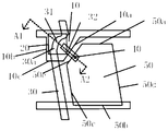
图1为本发明实施例1的阵列基板的示意图;1 is a schematic view of an array substrate according to
图2为图1中一个像素单元的示意图;Figure 2 is a schematic view of a pixel unit of Figure 1;
图3为本发明实施例1的夹角α和β的示意图;Figure 3 is a schematic view showing angles α and β of
图4为图2中的像素单元的A1-A2方向的截面图;Figure 4 is a cross-sectional view of the pixel unit of Figure 2 in the direction of A1-A2;
图5为本发明实施例2的阵列基板的示意图;5 is a schematic diagram of an array substrate according to
图6为图5中一个像素单元的示意图;以及Figure 6 is a schematic diagram of one pixel unit of Figure 5;
图7为图6中的像素单元的A1-A2方向的截面图。 Fig. 7 is a cross-sectional view taken along the line A1-A2 of the pixel unit of Fig. 6.
其中附图标记为:The reference numerals are:
1:衬底;1: substrate;
Gi:第i行栅线;Gi+1:第i+1行栅线;Gi-1:第i-1行栅线;Gi: the i-th row gate line; Gi+1: the i+1th-row gate line; Gi-1: the i-1th-row gate line;
Dj-1:第j-1列数据线;Dj:第j列数据线;Dj+1:第j+1列数据线;Dj-1: data line of the j-1th column; Dj: the data line of the jth column; Dj+1: the data line of the j+1th column;
CLi-1:第i-1行公共电极线;CLi:第i行公共电极线;CLi+1:第i+1行公共电极线;CLi-1: common electrode line of the i-1th row; CLi: common electrode line of the i-th row; CLi+1: common electrode line of the i+1th row;
15:栅极绝缘层;15: a gate insulating layer;
25:钝化层;25: passivation layer;
10:栅线的凸起结构;10a:栅线的凸起结构的一侧边;10b:栅线的凸起结构的另一侧边;10c:栅线的凸起结构的顶边;10: a convex structure of the gate line; 10a: one side of the convex structure of the gate line; 10b: the other side of the convex structure of the gate line; 10c: a top side of the convex structure of the gate line;
20:有源层;20: active layer;
30:数据线线段;31:源极;32:漏极;30: data line segment; 31: source; 32: drain;
30a:连接部;30a: a connection portion;
40:钝化层过孔;40: passivation layer via hole;
50:像素电极;50a:第一边;50b:第二边;50c:第三边;50d:第四边;50e:第五边;50: pixel electrode; 50a: first side; 50b: second side; 50c: third side; 50d: fourth side; 50e: fifth side;
60:公共电极;60a:狭缝。60: common electrode; 60a: slit.
为使本领域技术人员更好地理解本发明的技术方案,下面结合附图和具体实施方式对本发明作进一步详细描述。The present invention will be further described in detail below in conjunction with the accompanying drawings and specific embodiments.
实施例1:Example 1:
如图1-4所示,本实施例提供一种阵列基板,该阵列基板包括交叉设置的多条栅线(例如Gi-1、Gi、Gi+1)和多条数据线(例如Dj-1、Dj、Dj+1),以及由相邻栅线和相邻数据线限定的像素单元,每条数据线包括多个数据线线段30,每一数据线线段30对应一个像素单元,且同一数据线的两相邻的数据线线段30通过
连接部30a连接;所述栅线的延伸方向与所述数据线线段30的延伸方向的夹角为α;其中,60°≤α≤87°;所述薄膜晶体管的栅极为栅线的凸起结构10,所述凸起结构10的靠近像素电极的一侧边的延伸方向与所述栅线的延伸方向的夹角为β,其中,20°≤β≤70°。As shown in FIG. 1-4, the embodiment provides an array substrate including a plurality of gate lines (eg, Gi-1, Gi, Gi+1) and a plurality of data lines (for example, Dj-1). , Dj, Dj+1), and pixel cells defined by adjacent gate lines and adjacent data lines, each data line includes a plurality of
由于本实施例阵列基板的栅线的延伸方向和数据线线段30的延伸方向的夹角为α,60°≤α≤87°,所述凸起结构的靠近像素电极的一侧边的延伸方向与所述栅线的延伸方向的夹角为β,20°≤β≤70°,因此该阵列基板可以得到一个优化的视角方向、较高的开口率和较好的显示质量。Since the angle between the extending direction of the gate line of the array substrate and the extending direction of the
本实施例所提供的阵列基板可应用于TN模式的显示装置中。The array substrate provided in this embodiment can be applied to a display device of a TN mode.
具体的,如图2和图3所示,以由第i行栅线Gi、i+1行栅线Gi+1、第j列数据线Dj、第j+1列数据线Dj+1限定的像素单元Pij为例,其中,与栅线Gi平行的是公共电极线CLi,像素单元Pij包括薄膜晶体管、像素电极50,与该像素电极对应的数据线线段30,数据线线段30的延伸方向与栅线Gi的延伸方向的夹角为α,薄膜晶体管的栅极为栅线Gi的凸起结构10,所述凸起结构10的靠近像素电极50的一侧边10a的延伸方向与所述栅线Gi的延伸方向的夹角为β。Specifically, as shown in FIG. 2 and FIG. 3, the row is defined by the i-th row gate line Gi, i+1 row gate line Gi+1, the j-th column data line Dj, and the j+1th column data
其中,60°≤α≤87°,20°≤β≤70°。进一步优选地,70°≤α≤85°,30°≤β≤50°。Among them, 60 ° ≤ α ≤ 87 °, 20 ° ≤ β ≤ 70 °. Further preferably, 70° ≤ α ≤ 85°, 30° ≤ β ≤ 50°.
其中,本实施例的像素电极50为板状电极,其包括第一边50a、第二边50b、第三边50c、第四边50d和第五边50e;其中,所述第一边50a和所述第二边50b平行于所述栅线Gi的延伸方向;所述第三边50c和所述第四边50d平行于所述数据线线段30的延伸方向;所述第五边50e平行于所述凸起结构10的靠近像素电极50的一侧边10a的延伸方向。所述栅线的凸起结构10的另一侧边10b位于以该凸起结构10作为栅极的薄膜晶体管所在的像素单元的外侧。所述栅线的凸起结构10的顶边10c与以该凸起结构作为栅极的薄膜晶体管所在的像素单元对应的数据线线段交叠。此时,
不仅可以保证阵列基板较大的开口率,而且还充分利用了像素区的空间。The
如图2和图4所示,在薄膜晶体管源极31和漏极32所在层与像素电极50所在层之间设置有钝化层25,像素电极50通过贯穿钝化层25的过孔40与薄膜晶体管的漏极32连接。薄膜晶体管的源极31为所述数据线Dj的连接部30a,或者薄膜晶体管的源极31为所述连接部30a的一部分,特别的是,本实施例中所述数据线Dj的连接部30a的形状为曲线段。需要说明的是,像素电极50也可以设置在栅极绝缘层15上,像素电极50与薄膜晶体管的漏极32也可以采用直接搭接的方式连接。As shown in FIG. 2 and FIG. 4, a
本实施例中,同一条数据线的对应不同像素单元的数据线线段30的延伸方向相互平行。In this embodiment, the extending directions of the
相应的,本实施例还针对上述阵列基板提供了一种阵列基板的制备方法,其包括如下步骤:Correspondingly, the embodiment further provides a method for preparing an array substrate for the array substrate, which comprises the following steps:
步骤一、在衬底1上采用溅射的方法沉积一层栅极金属层薄膜,通过构图工艺形成薄膜晶体管栅极、栅线和公共电极线的图形,使得所述栅极为所述栅线的凸起结构。Step 1: depositing a gate metal layer film on the
需要说明的是,衬底1既可以指没有形成任何膜层的衬底,如白玻璃,也可以指形成有其他膜层或者图案的衬底,例如形成有缓冲层的衬底。构图工艺通常包括光刻胶涂敷、曝光、显影、刻蚀、光刻胶剥离等工艺。It should be noted that the
其中,所述栅极金属层薄膜的材料可以为钼(Mo)、钼铌合金(MoNb)、铝(Al)、铝钕合金(AlNd)、钛(Ti)和铜(Cu)中的一种或它们中多种材料形成的单层或多层复合叠层,优选为Mo、Al或含Mo、Al的合金组成的单层或多层复合膜。The material of the gate metal layer film may be one of molybdenum (Mo), molybdenum-niobium alloy (MoNb), aluminum (Al), aluminum-niobium alloy (AlNd), titanium (Ti), and copper (Cu). Or a single layer or a multilayer composite laminate formed of a plurality of materials thereof, preferably a single layer or a multilayer composite film composed of Mo, Al or an alloy containing Mo or Al.
步骤二、在完成上述步骤的衬底1上,采用化学气相沉积、等离子辅助化学气相淀积或溅射等制备方法,形成栅极绝缘层15。Step 2: On the
其中,所述栅极绝缘层15的材料可以为硅的氧化物(SiOx)、硅的氮化物(SiNx)、铪的氧化物(HfOx)、硅的氮氧化物(SiON)、铝的氧化物(AlOx)等中的一种或它们中两种材料组成的多层复
合膜。The material of the
步骤三、在完成上述步骤的衬底1上,通过化学气相沉积、等离子辅助化学气相淀积或溅射等制备方法沉积薄膜晶体管的有源层薄膜,通过构图工艺形成薄膜晶体管的有源层20的图形。Step 3: On the
其中,有源层20的材料可以为非晶硅、多晶硅、微晶硅或者氧化物半导体。The material of the
步骤四、在完成上述步骤的衬底1上,采用溅射的方法形成源漏金属层薄膜,并通过构图工艺形成薄膜晶体管源极31、漏极32和数据线的图形,使得所述栅线的延伸方向与所述数据线的延伸方向的夹角为α,其中,60°≤α≤87°。Step 4: forming a source/drain metal layer thin film on the
其中,所述源漏金属层薄膜的材料可以是钼(Mo)、钼铌合金(MoNb)、铝(Al)、铝钕合金(AlNd)、钛(Ti)和铜(Cu)中的一种或多种材料形成的,优选为Mo、Al或含Mo、Al的合金材料。The material of the source/drain metal layer film may be one of molybdenum (Mo), molybdenum-niobium alloy (MoNb), aluminum (Al), aluminum-niobium alloy (AlNd), titanium (Ti), and copper (Cu). Or formed of a plurality of materials, preferably Mo, Al or an alloy material containing Mo or Al.
步骤五、在完成上述步骤的衬底1上,采用化学气相沉积、等离子辅助化学气相淀积、或溅射等制备方法,形成钝化层25,并形成贯穿薄膜晶体管的漏极上方的钝化层25的过孔40。Step 5: On the
其中,钝化层的材料为硅的氧化物(SiOx)、硅的氮化物(SiNx)、铪的氧化物(HfOx)、硅的氮氧化物(SiON)、铝的氧化物(AlOx)等中的一种或它们中两种材料组成的多层复合膜。The material of the passivation layer is silicon oxide (SiOx), silicon nitride (SiNx), germanium oxide (HfOx), silicon nitrogen oxide (SiON), aluminum oxide (AlOx), and the like. A multilayer composite film of one or two of them.
步骤六,在完成上述步骤的衬底1上,采用溅射的方法沉积透明导电金属氧化物膜。然后,通过构图工艺,形成像素电极50的图形,使得像素电极50通过钝化层25的过孔40与漏极32连接,并且所述凸起结构的靠近所述像素电极50的一侧边的延伸方向与所述栅线的延伸方向的夹角为β,其中,20°≤β≤70°。Step 6. On the
其中,透明导电金属氧化物膜的材料为ITO(氧化铟锡)、IZO(氧化铟锌)、IGZO(氧化铟镓锌)或InGaSnO(氧化铟镓锡)。The material of the transparent conductive metal oxide film is ITO (indium tin oxide), IZO (indium zinc oxide), IGZO (indium gallium zinc oxide) or InGaSnO (indium gallium tin oxide).
至此完成阵列基板的制备。 This completes the preparation of the array substrate.
实施例2:Example 2:
如图5至图7所示,本实施例提供一种阵列基板,该阵列基板包括交叉设置的多条栅线(例如Gi-1、Gi、Gi+1)和多条数据线(例如Dj-1、Dj、Dj+1),以及由相邻栅线和相邻数据线限定的像素单元,每条数据线包括多个数据线线段30,每一数据线线段30对应一个像素单元,且同一数据线的两相邻的数据线线段30通过连接部30a连接;所述栅线的延伸方向与所述数据线线段30的延伸方向的夹角为α;其中,60°≤α≤87°;所述薄膜晶体管的栅极为栅线的凸起结构10,所述凸起结构的靠近像素电极的一侧边的延伸方向与所述栅线的延伸方向的夹角为β,其中,20°≤β≤70°。As shown in FIG. 5 to FIG. 7 , the embodiment provides an array substrate including a plurality of gate lines (eg, Gi-1, Gi, Gi+1) and a plurality of data lines (eg, Dj-) disposed at intersections. 1. Dj, Dj+1), and pixel cells defined by adjacent gate lines and adjacent data lines, each data line comprising a plurality of
由于本实施例阵列基板的栅线的延伸方向和数据线线段30的延伸方向的夹角为α,60°≤α≤87°,所述凸起结构的靠近像素电极的一侧边的延伸方向与所述栅线的延伸方向的夹角为β,20°≤β≤70°,因此该阵列基板可以得到一个优化的视角方向、较高的开口率和较好的显示质量。Since the angle between the extending direction of the gate line of the array substrate and the extending direction of the
本实施例所提供的阵列基板可应用于FFS模式的显示装置中。The array substrate provided in this embodiment can be applied to a display device of an FFS mode.
具体的,如图5和图6所示,以由第i行栅线Gi、i+1行栅线Gi+1、第j列数据线Dj、第j+1列数据线Dj+1限定的像素单元Pij为例,其中,与栅线Gi平行的是公共电极线CLi,像素单元Pij包括薄膜晶体管、像素电极50,与该像素电极对应的数据线线段30,数据线线段30的延伸方向与栅线Gi的延伸方向的夹角则为α,薄膜晶体管的栅极为栅线Gi的凸起结构10,所述凸起结构10的靠近像素电极50的一侧边10a的延伸方向与所述栅线Gi的延伸方向的夹角为β。Specifically, as shown in FIG. 5 and FIG. 6, the row is defined by the i-th row gate line Gi, i+1, the gate line Gi+1, the j-th column data line Dj, and the j+1th column data
其中,60°≤α≤87°,20°≤β≤70°。进一步优选地,70°≤α≤85°,30°≤β≤50°。Among them, 60 ° ≤ α ≤ 87 °, 20 ° ≤ β ≤ 70 °. Further preferably, 70° ≤ α ≤ 85°, 30° ≤ β ≤ 50°.
其中,本实施例的像素电极50为板状电极,其包括第一边50a、第二边50b、第三边50c、第四边50d和第五边50e;其中,
所述第一边50a和所述第二边50b平行于所述栅线Gi的延伸方向;所述第三边50c和所述第四边50d平行于所述数据线线段30的延伸方向;所述第五边50e平行于所述凸起结构10的靠近像素电极50的一侧边10a的延伸方向。所述栅线的凸起结构10的另一侧边10b位于以该凸起结构10作为栅极的薄膜晶体管所在的像素单元的外侧。所述栅线的凸起结构10的顶边10c与以该凸起结构10作为栅极的薄膜晶体管所在的像素单元对应的数据线线段交叠。此时,不仅可以保证阵列基板较大的开口率,而且还充分利用了像素区的空间。The
其中,如图7所示,像素电极50和薄膜晶体管的漏极32采用直接搭接的方式连接。薄膜晶体管的源极31为所述数据线Dj的连接部30a,或者薄膜晶体管的源极31为所述连接部30a的一部分,特别的是,本实施例中所述数据线Dj的连接部30a的形状为曲线线段。As shown in FIG. 7, the
其中,本实施例中同一条数据线的对应不同像素单元的数据线线段30的延伸方向相互平行。The extending direction of the
其中,阵列基板还包括公共电极60,公共电极60设于所述像素电极50上方,且与所述像素电极50绝缘;所述公共电极60具有狭缝60a,所述狭缝60a的延伸方向平行于所述数据线线段30的延伸方向。需要说明的是,狭缝60a的延伸方向应当理解为狭缝主体的中间线的延伸方向,狭缝主体不包括狭缝60a两端的部分,狭缝60a的端部的形状与狭缝主体部分相比可能会有些变化,以便更好控制液晶分子的排列。The array substrate further includes a
相应的,本实施例还针对上述阵列基板提供了一种阵列基板的制备方法,其包括如下步骤:Correspondingly, the embodiment further provides a method for preparing an array substrate for the array substrate, which comprises the following steps:
步骤一、在衬底1上采用溅射的方法沉积一层栅极金属层薄膜,通过构图工艺形成包括薄膜晶体管栅极、栅线和公共电极线的图形,使得所述栅极为所述栅线的凸起结构。Step 1: depositing a gate metal layer film on the
需要说明的是,衬底1既可以指没有形成任何膜层的衬底,如白玻璃,也可以指形成有其他膜层或者图案的衬底,例如形成
有缓冲层的衬底。构图工艺通常包括光刻胶涂敷、曝光、显影、刻蚀、光刻胶剥离等工艺。It should be noted that the
其中,所述栅极金属层薄膜的材料可以为钼(Mo)、钼铌合金(MoNb)、铝(Al)、铝钕合金(AlNd)、钛(Ti)和铜(Cu)中的一种或它们中多种材料形成的单层或多层复合叠层,优选为Mo、Al或含Mo、Al的合金组成的单层或多层复合膜。The material of the gate metal layer film may be one of molybdenum (Mo), molybdenum-niobium alloy (MoNb), aluminum (Al), aluminum-niobium alloy (AlNd), titanium (Ti), and copper (Cu). Or a single layer or a multilayer composite laminate formed of a plurality of materials thereof, preferably a single layer or a multilayer composite film composed of Mo, Al or an alloy containing Mo or Al.
步骤二、在完成上述步骤的衬底1上,采用化学气相沉积、等离子辅助化学气相淀积或溅射等制备方法,形成栅极绝缘层15。Step 2: On the
其中,所述栅极绝缘层15的材料可以为硅的氧化物(SiOx)、硅的氮化物(SiNx)、铪的氧化物(HfOx)、硅的氮氧化物(SiON)、铝的氧化物(AlOx)等中的一种或它们中两种材料组成的多层复合膜。The material of the
步骤三,在完成上述步骤的衬底1上,采用溅射的方法沉积透明导电金属氧化物膜。然后,通过构图工艺,形成像素电极50的图形,使得所述凸起结构的靠近所述像素电极50的一侧边的延伸方向与所述栅线的延伸方向的夹角为β,其中,20°≤β≤70°。Step 3, on the
其中,透明导电金属氧化物膜的材料为ITO(氧化铟锡)、IZO(氧化铟锌)、IGZO(氧化铟镓锌)或InGaSnO(氧化铟镓锡)。The material of the transparent conductive metal oxide film is ITO (indium tin oxide), IZO (indium zinc oxide), IGZO (indium gallium zinc oxide) or InGaSnO (indium gallium tin oxide).
步骤四、在完成上述步骤的衬底1上,通过化学气相沉积、等离子辅助化学气相淀积或溅射等制备方法沉积薄膜晶体管的有源层薄膜,通过构图工艺形成薄膜晶体管的有源层的图形。Step 4, on the
其中,有源层20的材料可以为非晶硅、多晶硅、微晶硅或者氧化物半导体。The material of the
步骤五、在完成上述步骤的衬底1上,采用溅射的方法形成源漏金属层薄膜,并通过构图工艺形成薄膜晶体管源极31、漏极32和数据线的图形,使得薄膜晶体管的漏极32与像素电极直接搭接,所述栅线的延伸方向与所述数据线的延伸方向的夹角为α,其中,60°≤α≤87°。Step 5: On the
其中,所述源漏金属层薄膜的材料可以是钼(Mo)、钼铌合 金(MoNb)、铝(Al)、铝钕合金(AlNd)、钛(Ti)和铜(Cu)中的一种或多种材料形成的,优选为Mo、Al或含Mo、Al的合金材料。Wherein, the material of the source/drain metal layer film may be molybdenum (Mo) or molybdenum Formed from one or more of gold (MoNb), aluminum (Al), aluminum-niobium alloy (AlNd), titanium (Ti), and copper (Cu), preferably Mo, Al or alloy materials containing Mo, Al .
步骤六、在完成上述步骤的衬底1上,采用化学气相沉积、等离子辅助化学气相淀积、或溅射等制备方法,形成钝化层25。Step 6. On the
其中,钝化层的材料为硅的氧化物(SiOx)、硅的氮化物(SiNx)、铪的氧化物(HfOx)、硅的氮氧化物(SiON)、铝的氧化物(AlOx)等中的一种或它们中两种材料组成的多层复合膜。The material of the passivation layer is silicon oxide (SiOx), silicon nitride (SiNx), germanium oxide (HfOx), silicon nitrogen oxide (SiON), aluminum oxide (AlOx), and the like. A multilayer composite film of one or two of them.
步骤七、在完成上述步骤的衬底1上,采用溅射的方法沉积透明导电金属氧化物膜。然后,通过构图工艺,形成公共电极60的图形,使得所述公共电极60设置于所述像素电极50上方,且与所述像素电极50绝缘,所述公共电极60具有狭缝,所述狭缝的延伸方向平行于所述数据线的延伸方向。Step 7. On the
其中,透明导电金属氧化物膜的材料为ITO(氧化铟锡)、IZO(氧化铟锌)、IGZO(氧化铟镓锌)或InGaSnO(氧化铟镓锡)。The material of the transparent conductive metal oxide film is ITO (indium tin oxide), IZO (indium zinc oxide), IGZO (indium gallium zinc oxide) or InGaSnO (indium gallium tin oxide).
至此完成阵列基板的制备。This completes the preparation of the array substrate.
实施例3:Example 3:
本实施例提供一种显示装置,其包括上述阵列基板以及与阵列基板对盒设置的对盒基板。其中,当阵列基板采用实施例1所述的阵列基板时,该显示装置为TN模式的显示装置,此时对盒基板上还设置有公共电极。当阵列基板采用实施例2所述的阵列基板时,该显示装置为FFS模式的显示装置。The embodiment provides a display device including the array substrate and the pair of cassette substrates disposed on the array substrate. Wherein, when the array substrate is the array substrate described in
其中,显示装置可以为液晶显示装置或者电致发光显示装置,例如液晶面板、电子纸、手机、平板电脑、电视机、显示器、笔记本电脑、数码相框、导航仪等任何具有显示功能的产品或部件。The display device may be a liquid crystal display device or an electroluminescence display device, such as a liquid crystal panel, an electronic paper, a mobile phone, a tablet computer, a television, a display, a notebook computer, a digital photo frame, a navigator, or the like, or any display product or component. .
本实施例中的显示装置具有优化的视角方向、较高的开口率和较好的显示质量。 The display device in this embodiment has an optimized viewing angle direction, a high aperture ratio, and a good display quality.
可以理解的是,以上实施方式仅仅是为了说明本发明的原理而采用的示例性实施方式,然而本发明并不局限于此。对于本领域内的普通技术人员而言,在不脱离本发明的精神和实质的情况下,可以做出各种变型和改进,这些变型和改进也视为本发明的保护范围。 It is to be understood that the above embodiments are merely exemplary embodiments employed to explain the principles of the invention, but the invention is not limited thereto. Various modifications and improvements can be made by those skilled in the art without departing from the spirit and scope of the invention. These modifications and improvements are also considered to be within the scope of the invention.
Claims (15)
Priority Applications (1)
| Application Number | Priority Date | Filing Date | Title |
|---|---|---|---|
| US14/912,224 US10234737B2 (en) | 2015-03-11 | 2015-09-17 | Array substrate and manufacturing method thereof, and display device |
Applications Claiming Priority (2)
| Application Number | Priority Date | Filing Date | Title |
|---|---|---|---|
| CN201510106509.9A CN104637958B (en) | 2015-03-11 | 2015-03-11 | Array base palte and display device |
| CN201510106509.9 | 2015-03-11 |
Publications (1)
| Publication Number | Publication Date |
|---|---|
| WO2016141705A1 true WO2016141705A1 (en) | 2016-09-15 |
Family
ID=53216499
Family Applications (1)
| Application Number | Title | Priority Date | Filing Date |
|---|---|---|---|
| PCT/CN2015/089834 Ceased WO2016141705A1 (en) | 2015-03-11 | 2015-09-17 | Array substrate and manufacturing method thereof, and display device |
Country Status (3)
| Country | Link |
|---|---|
| US (1) | US10234737B2 (en) |
| CN (1) | CN104637958B (en) |
| WO (1) | WO2016141705A1 (en) |
Cited By (1)
| Publication number | Priority date | Publication date | Assignee | Title |
|---|---|---|---|---|
| CN112420737A (en) * | 2019-08-20 | 2021-02-26 | 友达光电股份有限公司 | Pixel array substrate |
Families Citing this family (8)
| Publication number | Priority date | Publication date | Assignee | Title |
|---|---|---|---|---|
| CN104216129B (en) * | 2014-09-12 | 2017-08-11 | 上海天马微电子有限公司 | Display panel and display device |
| CN104637958B (en) * | 2015-03-11 | 2017-10-17 | 京东方科技集团股份有限公司 | Array base palte and display device |
| CN112034656B (en) * | 2020-09-11 | 2022-08-26 | 合肥鑫晟光电科技有限公司 | Array substrate and display device |
| KR20240007175A (en) * | 2021-05-13 | 2024-01-16 | 가부시키가이샤 한도오따이 에네루기 켄큐쇼 | Semiconductor device, display device, and method of manufacturing semiconductor device |
| EP4339699A4 (en) * | 2021-08-31 | 2024-07-24 | BOE Technology Group Co., Ltd. | DISPLAY SUBSTRATE AND DISPLAY BOARD |
| CN114355641B (en) * | 2021-12-31 | 2024-01-26 | 惠科股份有限公司 | Array substrate, display panel and display device |
| CN114694519B (en) * | 2022-04-24 | 2023-10-20 | 湖北长江新型显示产业创新中心有限公司 | Panel splicing system and panel splicing method |
| CN115032842B (en) * | 2022-07-01 | 2023-11-28 | 武汉华星光电技术有限公司 | Display panel and display terminal |
Citations (8)
| Publication number | Priority date | Publication date | Assignee | Title |
|---|---|---|---|---|
| US20040156005A1 (en) * | 2001-02-26 | 2004-08-12 | Yun-Bok Lee | Array substrate for in-plane switching mode liquid crystal display device and manufacturing method thereof |
| CN1577019A (en) * | 2003-06-26 | 2005-02-09 | 三星电子株式会社 | Liquid crystal display and thin film transistor array panel therefor |
| CN1580923A (en) * | 2003-07-31 | 2005-02-16 | 三星电子株式会社 | Multi-zone liquid crystal display |
| CN101093329A (en) * | 2006-06-21 | 2007-12-26 | Lg.菲利浦Lcd株式会社 | Array substrate for in-plane switching mode liquid crystal display device and method of fabricating the same |
| US20100066933A1 (en) * | 2008-09-17 | 2010-03-18 | Samsung Electronics Co., Ltd. | Display plate and liquid crystal display device having the same |
| CN102945827A (en) * | 2012-11-14 | 2013-02-27 | 京东方科技集团股份有限公司 | Array substrate and manufacturing method thereof |
| CN104122714A (en) * | 2013-07-11 | 2014-10-29 | 深超光电(深圳)有限公司 | Array substrate of a liquid crystal display |
| CN104637958A (en) * | 2015-03-11 | 2015-05-20 | 京东方科技集团股份有限公司 | Array base plate and display device |
Family Cites Families (13)
| Publication number | Priority date | Publication date | Assignee | Title |
|---|---|---|---|---|
| US4968119A (en) * | 1989-01-10 | 1990-11-06 | David Sarnoff Research Center, Inc. | High-density liquid-crystal active dot-matrix display structure |
| KR970004883B1 (en) * | 1992-04-03 | 1997-04-08 | 삼성전자 주식회사 | Liquid crystal display panel |
| JP3507117B2 (en) * | 1993-02-26 | 2004-03-15 | キヤノン株式会社 | TFT substrate and liquid crystal display device having the substrate |
| US6791647B1 (en) * | 1999-02-24 | 2004-09-14 | Lg Philips Lcd Co., Ltd. | Multi-domain liquid crystal display device |
| KR100710282B1 (en) * | 2000-12-29 | 2007-04-23 | 엘지.필립스 엘시디 주식회사 | Thin film transistor and its manufacturing method |
| KR20040105934A (en) * | 2003-06-10 | 2004-12-17 | 삼성전자주식회사 | Liquid crystal display having multi domain and panel for the same |
| US7202928B2 (en) | 2003-10-16 | 2007-04-10 | Lg. Philips Lcd Co., Ltd | Array substrate for in-plane switching mode liquid crystal display device and method of fabricating the same |
| KR101309139B1 (en) * | 2003-12-29 | 2013-09-17 | 엘지디스플레이 주식회사 | array substrate and liquid crystal display device including the same |
| KR100789091B1 (en) * | 2004-06-30 | 2007-12-26 | 엘지.필립스 엘시디 주식회사 | Transverse electric field type liquid crystal display device and manufacturing method thereof |
| TWI248684B (en) * | 2004-11-26 | 2006-02-01 | Innolux Display Corp | Liquid crystal display device |
| KR20120066950A (en) * | 2010-12-15 | 2012-06-25 | 삼성전자주식회사 | Echtant, display device and method for manufacturing display device using the same |
| JP5900818B2 (en) * | 2011-03-29 | 2016-04-06 | Nltテクノロジー株式会社 | Liquid crystal display |
| JP6061266B2 (en) | 2012-10-19 | 2017-01-18 | Nltテクノロジー株式会社 | Liquid crystal display |
-
2015
- 2015-03-11 CN CN201510106509.9A patent/CN104637958B/en active Active
- 2015-09-17 US US14/912,224 patent/US10234737B2/en active Active
- 2015-09-17 WO PCT/CN2015/089834 patent/WO2016141705A1/en not_active Ceased
Patent Citations (8)
| Publication number | Priority date | Publication date | Assignee | Title |
|---|---|---|---|---|
| US20040156005A1 (en) * | 2001-02-26 | 2004-08-12 | Yun-Bok Lee | Array substrate for in-plane switching mode liquid crystal display device and manufacturing method thereof |
| CN1577019A (en) * | 2003-06-26 | 2005-02-09 | 三星电子株式会社 | Liquid crystal display and thin film transistor array panel therefor |
| CN1580923A (en) * | 2003-07-31 | 2005-02-16 | 三星电子株式会社 | Multi-zone liquid crystal display |
| CN101093329A (en) * | 2006-06-21 | 2007-12-26 | Lg.菲利浦Lcd株式会社 | Array substrate for in-plane switching mode liquid crystal display device and method of fabricating the same |
| US20100066933A1 (en) * | 2008-09-17 | 2010-03-18 | Samsung Electronics Co., Ltd. | Display plate and liquid crystal display device having the same |
| CN102945827A (en) * | 2012-11-14 | 2013-02-27 | 京东方科技集团股份有限公司 | Array substrate and manufacturing method thereof |
| CN104122714A (en) * | 2013-07-11 | 2014-10-29 | 深超光电(深圳)有限公司 | Array substrate of a liquid crystal display |
| CN104637958A (en) * | 2015-03-11 | 2015-05-20 | 京东方科技集团股份有限公司 | Array base plate and display device |
Cited By (1)
| Publication number | Priority date | Publication date | Assignee | Title |
|---|---|---|---|---|
| CN112420737A (en) * | 2019-08-20 | 2021-02-26 | 友达光电股份有限公司 | Pixel array substrate |
Also Published As
| Publication number | Publication date |
|---|---|
| US20170045791A1 (en) | 2017-02-16 |
| CN104637958B (en) | 2017-10-17 |
| US10234737B2 (en) | 2019-03-19 |
| CN104637958A (en) | 2015-05-20 |
Similar Documents
| Publication | Publication Date | Title |
|---|---|---|
| CN105470269B (en) | TFT array substrate and manufacturing method thereof | |
| WO2016141705A1 (en) | Array substrate and manufacturing method thereof, and display device | |
| CN105405851B (en) | Thin film transistor substrate and manufacturing method thereof | |
| US8107029B2 (en) | Thin film transistor substrate | |
| CN103515394B (en) | There is thin film transistor base plate and the manufacture method thereof of metal-oxide semiconductor (MOS) | |
| US10217778B2 (en) | Array substrate and manufacturing method thereof | |
| CN204422935U (en) | A kind of array base palte and display device | |
| US20190051667A1 (en) | An array substrate and a manufacturing method thereof, a display panel, as well as a display device | |
| CN102955312A (en) | Array substrate and manufacture method thereof and display device | |
| US8885128B2 (en) | Liquid crystal display device and method for fabricating the same | |
| CN105633016A (en) | Manufacturing method of TFT substrate and prepared TFT substrate | |
| US10147744B2 (en) | Array substrate, method of manufacturing the same, and display device | |
| WO2013104300A1 (en) | Array substrate and display device comprising same | |
| CN107316875A (en) | Preparation method, array base palte and the liquid crystal panel of array base palte | |
| US8451410B2 (en) | Array substrate for wide viewing angle liquid crystal display device and mehod of manufacturing the same | |
| CN204028524U (en) | Display base plate and display device | |
| CN103309100A (en) | Liquid crystal display device and method of fabricating the same | |
| JP5016225B2 (en) | Array substrate, liquid crystal display panel having the same, and liquid crystal display device | |
| CN107978608A (en) | IPS type thin-film transistor array base-plates and preparation method thereof | |
| WO2018192052A1 (en) | Array substrate structure and method for manufacturing array substrate | |
| CN102929056B (en) | A kind of array base palte and manufacture method, display device | |
| CN103149754B (en) | Thin film transistor LCD device and manufacture method thereof | |
| WO2019100495A1 (en) | Ffs-type thin-film transistor array substrate and manufacturing method therefor | |
| CN105974687B (en) | Array substrate and liquid crystal display | |
| CN106575062A (en) | Active matrix substrate and method for producing same |
Legal Events
| Date | Code | Title | Description |
|---|---|---|---|
| WWE | Wipo information: entry into national phase |
Ref document number: 14912224 Country of ref document: US |
|
| 121 | Ep: the epo has been informed by wipo that ep was designated in this application |
Ref document number: 15884384 Country of ref document: EP Kind code of ref document: A1 |
|
| NENP | Non-entry into the national phase |
Ref country code: DE |
|
| 122 | Ep: pct application non-entry in european phase |
Ref document number: 15884384 Country of ref document: EP Kind code of ref document: A1 |
|
| 32PN | Ep: public notification in the ep bulletin as address of the adressee cannot be established |
Free format text: NOTING OF LOSS OF RIGHTS PURSUANT TO RULE 112(1) EPC (EPO FORM 1205A DATED 01/03/2018) |
|
| 122 | Ep: pct application non-entry in european phase |
Ref document number: 15884384 Country of ref document: EP Kind code of ref document: A1 |