WO2016046909A1 - 半導体装置の製造方法、基板処理装置、半導体装置およびプログラム - Google Patents
半導体装置の製造方法、基板処理装置、半導体装置およびプログラム Download PDFInfo
- Publication number
- WO2016046909A1 WO2016046909A1 PCT/JP2014/075232 JP2014075232W WO2016046909A1 WO 2016046909 A1 WO2016046909 A1 WO 2016046909A1 JP 2014075232 W JP2014075232 W JP 2014075232W WO 2016046909 A1 WO2016046909 A1 WO 2016046909A1
- Authority
- WO
- WIPO (PCT)
- Prior art keywords
- gas
- layer
- film
- substrate
- metal layer
- Prior art date
- Legal status (The legal status is an assumption and is not a legal conclusion. Google has not performed a legal analysis and makes no representation as to the accuracy of the status listed.)
- Ceased
Links
Images


Classifications
-
- C—CHEMISTRY; METALLURGY
- C23—COATING METALLIC MATERIAL; COATING MATERIAL WITH METALLIC MATERIAL; CHEMICAL SURFACE TREATMENT; DIFFUSION TREATMENT OF METALLIC MATERIAL; COATING BY VACUUM EVAPORATION, BY SPUTTERING, BY ION IMPLANTATION OR BY CHEMICAL VAPOUR DEPOSITION, IN GENERAL; INHIBITING CORROSION OF METALLIC MATERIAL OR INCRUSTATION IN GENERAL
- C23C—COATING METALLIC MATERIAL; COATING MATERIAL WITH METALLIC MATERIAL; SURFACE TREATMENT OF METALLIC MATERIAL BY DIFFUSION INTO THE SURFACE, BY CHEMICAL CONVERSION OR SUBSTITUTION; COATING BY VACUUM EVAPORATION, BY SPUTTERING, BY ION IMPLANTATION OR BY CHEMICAL VAPOUR DEPOSITION, IN GENERAL
- C23C16/00—Chemical coating by decomposition of gaseous compounds, without leaving reaction products of surface material in the coating, i.e. chemical vapour deposition [CVD] processes
- C23C16/44—Chemical coating by decomposition of gaseous compounds, without leaving reaction products of surface material in the coating, i.e. chemical vapour deposition [CVD] processes characterised by the method of coating
- C23C16/455—Chemical coating by decomposition of gaseous compounds, without leaving reaction products of surface material in the coating, i.e. chemical vapour deposition [CVD] processes characterised by the method of coating characterised by the method used for introducing gases into reaction chamber or for modifying gas flows in reaction chamber
- C23C16/45523—Pulsed gas flow or change of composition over time
- C23C16/45525—Atomic layer deposition [ALD]
- C23C16/45527—Atomic layer deposition [ALD] characterized by the ALD cycle, e.g. different flows or temperatures during half-reactions, unusual pulsing sequence, use of precursor mixtures or auxiliary reactants or activations
-
- C—CHEMISTRY; METALLURGY
- C23—COATING METALLIC MATERIAL; COATING MATERIAL WITH METALLIC MATERIAL; CHEMICAL SURFACE TREATMENT; DIFFUSION TREATMENT OF METALLIC MATERIAL; COATING BY VACUUM EVAPORATION, BY SPUTTERING, BY ION IMPLANTATION OR BY CHEMICAL VAPOUR DEPOSITION, IN GENERAL; INHIBITING CORROSION OF METALLIC MATERIAL OR INCRUSTATION IN GENERAL
- C23C—COATING METALLIC MATERIAL; COATING MATERIAL WITH METALLIC MATERIAL; SURFACE TREATMENT OF METALLIC MATERIAL BY DIFFUSION INTO THE SURFACE, BY CHEMICAL CONVERSION OR SUBSTITUTION; COATING BY VACUUM EVAPORATION, BY SPUTTERING, BY ION IMPLANTATION OR BY CHEMICAL VAPOUR DEPOSITION, IN GENERAL
- C23C16/00—Chemical coating by decomposition of gaseous compounds, without leaving reaction products of surface material in the coating, i.e. chemical vapour deposition [CVD] processes
- C23C16/02—Pretreatment of the material to be coated
- C23C16/0272—Deposition of sub-layers, e.g. to promote the adhesion of the main coating
- C23C16/0281—Deposition of sub-layers, e.g. to promote the adhesion of the main coating of metallic sub-layers
-
- C—CHEMISTRY; METALLURGY
- C23—COATING METALLIC MATERIAL; COATING MATERIAL WITH METALLIC MATERIAL; CHEMICAL SURFACE TREATMENT; DIFFUSION TREATMENT OF METALLIC MATERIAL; COATING BY VACUUM EVAPORATION, BY SPUTTERING, BY ION IMPLANTATION OR BY CHEMICAL VAPOUR DEPOSITION, IN GENERAL; INHIBITING CORROSION OF METALLIC MATERIAL OR INCRUSTATION IN GENERAL
- C23C—COATING METALLIC MATERIAL; COATING MATERIAL WITH METALLIC MATERIAL; SURFACE TREATMENT OF METALLIC MATERIAL BY DIFFUSION INTO THE SURFACE, BY CHEMICAL CONVERSION OR SUBSTITUTION; COATING BY VACUUM EVAPORATION, BY SPUTTERING, BY ION IMPLANTATION OR BY CHEMICAL VAPOUR DEPOSITION, IN GENERAL
- C23C16/00—Chemical coating by decomposition of gaseous compounds, without leaving reaction products of surface material in the coating, i.e. chemical vapour deposition [CVD] processes
- C23C16/06—Chemical coating by decomposition of gaseous compounds, without leaving reaction products of surface material in the coating, i.e. chemical vapour deposition [CVD] processes characterised by the deposition of metallic material
- C23C16/08—Chemical coating by decomposition of gaseous compounds, without leaving reaction products of surface material in the coating, i.e. chemical vapour deposition [CVD] processes characterised by the deposition of metallic material from metal halides
- C23C16/14—Deposition of only one other metal element
-
- C—CHEMISTRY; METALLURGY
- C23—COATING METALLIC MATERIAL; COATING MATERIAL WITH METALLIC MATERIAL; CHEMICAL SURFACE TREATMENT; DIFFUSION TREATMENT OF METALLIC MATERIAL; COATING BY VACUUM EVAPORATION, BY SPUTTERING, BY ION IMPLANTATION OR BY CHEMICAL VAPOUR DEPOSITION, IN GENERAL; INHIBITING CORROSION OF METALLIC MATERIAL OR INCRUSTATION IN GENERAL
- C23C—COATING METALLIC MATERIAL; COATING MATERIAL WITH METALLIC MATERIAL; SURFACE TREATMENT OF METALLIC MATERIAL BY DIFFUSION INTO THE SURFACE, BY CHEMICAL CONVERSION OR SUBSTITUTION; COATING BY VACUUM EVAPORATION, BY SPUTTERING, BY ION IMPLANTATION OR BY CHEMICAL VAPOUR DEPOSITION, IN GENERAL
- C23C16/00—Chemical coating by decomposition of gaseous compounds, without leaving reaction products of surface material in the coating, i.e. chemical vapour deposition [CVD] processes
- C23C16/22—Chemical coating by decomposition of gaseous compounds, without leaving reaction products of surface material in the coating, i.e. chemical vapour deposition [CVD] processes characterised by the deposition of inorganic material, other than metallic material
- C23C16/30—Deposition of compounds, mixtures or solid solutions, e.g. borides, carbides, nitrides
- C23C16/34—Nitrides
-
- C—CHEMISTRY; METALLURGY
- C23—COATING METALLIC MATERIAL; COATING MATERIAL WITH METALLIC MATERIAL; CHEMICAL SURFACE TREATMENT; DIFFUSION TREATMENT OF METALLIC MATERIAL; COATING BY VACUUM EVAPORATION, BY SPUTTERING, BY ION IMPLANTATION OR BY CHEMICAL VAPOUR DEPOSITION, IN GENERAL; INHIBITING CORROSION OF METALLIC MATERIAL OR INCRUSTATION IN GENERAL
- C23C—COATING METALLIC MATERIAL; COATING MATERIAL WITH METALLIC MATERIAL; SURFACE TREATMENT OF METALLIC MATERIAL BY DIFFUSION INTO THE SURFACE, BY CHEMICAL CONVERSION OR SUBSTITUTION; COATING BY VACUUM EVAPORATION, BY SPUTTERING, BY ION IMPLANTATION OR BY CHEMICAL VAPOUR DEPOSITION, IN GENERAL
- C23C16/00—Chemical coating by decomposition of gaseous compounds, without leaving reaction products of surface material in the coating, i.e. chemical vapour deposition [CVD] processes
- C23C16/44—Chemical coating by decomposition of gaseous compounds, without leaving reaction products of surface material in the coating, i.e. chemical vapour deposition [CVD] processes characterised by the method of coating
- C23C16/455—Chemical coating by decomposition of gaseous compounds, without leaving reaction products of surface material in the coating, i.e. chemical vapour deposition [CVD] processes characterised by the method of coating characterised by the method used for introducing gases into reaction chamber or for modifying gas flows in reaction chamber
- C23C16/45523—Pulsed gas flow or change of composition over time
- C23C16/45525—Atomic layer deposition [ALD]
- C23C16/45527—Atomic layer deposition [ALD] characterized by the ALD cycle, e.g. different flows or temperatures during half-reactions, unusual pulsing sequence, use of precursor mixtures or auxiliary reactants or activations
- C23C16/45529—Atomic layer deposition [ALD] characterized by the ALD cycle, e.g. different flows or temperatures during half-reactions, unusual pulsing sequence, use of precursor mixtures or auxiliary reactants or activations specially adapted for making a layer stack of alternating different compositions or gradient compositions
-
- H—ELECTRICITY
- H10—SEMICONDUCTOR DEVICES; ELECTRIC SOLID-STATE DEVICES NOT OTHERWISE PROVIDED FOR
- H10D—INORGANIC ELECTRIC SEMICONDUCTOR DEVICES
- H10D64/00—Electrodes of devices having potential barriers
- H10D64/01—Manufacture or treatment
-
- H—ELECTRICITY
- H10—SEMICONDUCTOR DEVICES; ELECTRIC SOLID-STATE DEVICES NOT OTHERWISE PROVIDED FOR
- H10D—INORGANIC ELECTRIC SEMICONDUCTOR DEVICES
- H10D64/00—Electrodes of devices having potential barriers
- H10D64/20—Electrodes characterised by their shapes, relative sizes or dispositions
- H10D64/27—Electrodes not carrying the current to be rectified, amplified, oscillated or switched, e.g. gates
- H10D64/311—Gate electrodes for field-effect devices
- H10D64/411—Gate electrodes for field-effect devices for FETs
- H10D64/511—Gate electrodes for field-effect devices for FETs for IGFETs
- H10D64/517—Gate electrodes for field-effect devices for FETs for IGFETs characterised by the conducting layers
-
- H—ELECTRICITY
- H10—SEMICONDUCTOR DEVICES; ELECTRIC SOLID-STATE DEVICES NOT OTHERWISE PROVIDED FOR
- H10D—INORGANIC ELECTRIC SEMICONDUCTOR DEVICES
- H10D64/00—Electrodes of devices having potential barriers
- H10D64/60—Electrodes characterised by their materials
- H10D64/605—Source, drain, or gate electrodes for FETs comprising highly resistive materials
-
- H—ELECTRICITY
- H10—SEMICONDUCTOR DEVICES; ELECTRIC SOLID-STATE DEVICES NOT OTHERWISE PROVIDED FOR
- H10D—INORGANIC ELECTRIC SEMICONDUCTOR DEVICES
- H10D64/00—Electrodes of devices having potential barriers
- H10D64/60—Electrodes characterised by their materials
- H10D64/66—Electrodes having a conductor capacitively coupled to a semiconductor by an insulator, e.g. MIS electrodes
- H10D64/667—Electrodes having a conductor capacitively coupled to a semiconductor by an insulator, e.g. MIS electrodes the conductor comprising a layer of alloy material, compound material or organic material contacting the insulator, e.g. TiN workfunction layers
-
- H—ELECTRICITY
- H10—SEMICONDUCTOR DEVICES; ELECTRIC SOLID-STATE DEVICES NOT OTHERWISE PROVIDED FOR
- H10P—GENERIC PROCESSES OR APPARATUS FOR THE MANUFACTURE OR TREATMENT OF DEVICES COVERED BY CLASS H10
- H10P14/00—Formation of materials, e.g. in the shape of layers or pillars
- H10P14/40—Formation of materials, e.g. in the shape of layers or pillars of conductive or resistive materials
- H10P14/42—Formation of materials, e.g. in the shape of layers or pillars of conductive or resistive materials using a gas or vapour
- H10P14/43—Chemical deposition, e.g. chemical vapour deposition [CVD]
- H10P14/432—Chemical deposition, e.g. chemical vapour deposition [CVD] using selective deposition
-
- H—ELECTRICITY
- H10—SEMICONDUCTOR DEVICES; ELECTRIC SOLID-STATE DEVICES NOT OTHERWISE PROVIDED FOR
- H10W—GENERIC PACKAGES, INTERCONNECTIONS, CONNECTORS OR OTHER CONSTRUCTIONAL DETAILS OF DEVICES COVERED BY CLASS H10
- H10W20/00—Interconnections in chips, wafers or substrates
- H10W20/01—Manufacture or treatment
- H10W20/031—Manufacture or treatment of conductive parts of the interconnections
- H10W20/032—Manufacture or treatment of conductive parts of the interconnections of conductive barrier, adhesion or liner layers
- H10W20/033—Manufacture or treatment of conductive parts of the interconnections of conductive barrier, adhesion or liner layers in openings in dielectrics
-
- H—ELECTRICITY
- H10—SEMICONDUCTOR DEVICES; ELECTRIC SOLID-STATE DEVICES NOT OTHERWISE PROVIDED FOR
- H10W—GENERIC PACKAGES, INTERCONNECTIONS, CONNECTORS OR OTHER CONSTRUCTIONAL DETAILS OF DEVICES COVERED BY CLASS H10
- H10W20/00—Interconnections in chips, wafers or substrates
- H10W20/01—Manufacture or treatment
- H10W20/031—Manufacture or treatment of conductive parts of the interconnections
- H10W20/032—Manufacture or treatment of conductive parts of the interconnections of conductive barrier, adhesion or liner layers
- H10W20/042—Manufacture or treatment of conductive parts of the interconnections of conductive barrier, adhesion or liner layers the barrier, adhesion or liner layers being seed or nucleation layers
- H10W20/045—Manufacture or treatment of conductive parts of the interconnections of conductive barrier, adhesion or liner layers the barrier, adhesion or liner layers being seed or nucleation layers for deposition from the gaseous phase, e.g. for chemical vapour deposition [CVD]
-
- H—ELECTRICITY
- H10—SEMICONDUCTOR DEVICES; ELECTRIC SOLID-STATE DEVICES NOT OTHERWISE PROVIDED FOR
- H10W—GENERIC PACKAGES, INTERCONNECTIONS, CONNECTORS OR OTHER CONSTRUCTIONAL DETAILS OF DEVICES COVERED BY CLASS H10
- H10W20/00—Interconnections in chips, wafers or substrates
- H10W20/01—Manufacture or treatment
- H10W20/031—Manufacture or treatment of conductive parts of the interconnections
- H10W20/056—Manufacture or treatment of conductive parts of the interconnections by filling conductive material into holes, grooves or trenches
-
- H—ELECTRICITY
- H10—SEMICONDUCTOR DEVICES; ELECTRIC SOLID-STATE DEVICES NOT OTHERWISE PROVIDED FOR
- H10P—GENERIC PROCESSES OR APPARATUS FOR THE MANUFACTURE OR TREATMENT OF DEVICES COVERED BY CLASS H10
- H10P14/00—Formation of materials, e.g. in the shape of layers or pillars
- H10P14/40—Formation of materials, e.g. in the shape of layers or pillars of conductive or resistive materials
- H10P14/418—Formation of materials, e.g. in the shape of layers or pillars of conductive or resistive materials the conductive layers comprising transition metals
-
- H—ELECTRICITY
- H10—SEMICONDUCTOR DEVICES; ELECTRIC SOLID-STATE DEVICES NOT OTHERWISE PROVIDED FOR
- H10P—GENERIC PROCESSES OR APPARATUS FOR THE MANUFACTURE OR TREATMENT OF DEVICES COVERED BY CLASS H10
- H10P14/00—Formation of materials, e.g. in the shape of layers or pillars
- H10P14/40—Formation of materials, e.g. in the shape of layers or pillars of conductive or resistive materials
- H10P14/42—Formation of materials, e.g. in the shape of layers or pillars of conductive or resistive materials using a gas or vapour
- H10P14/43—Chemical deposition, e.g. chemical vapour deposition [CVD]
Definitions
- the present invention relates to a method for manufacturing a semiconductor device for forming a thin film on a substrate, a substrate processing apparatus, a semiconductor device, and a program.
- a metal film in an ultrafine groove having a narrower opening than before.
- a low resistivity is required for the metal film.
- the metal film for example, a control gate of a flash memory, a gate electrode of a DRAM (Dynamic Random Access to Memory), a wiring between the electrodes, and the like can be considered.
- the surface roughness (also simply referred to as roughness) may increase and voids may be generated.
- an amorphous film is used to reduce the surface roughness, it is necessary to lower the temperature during the film formation, and the resistivity of the obtained metal film is increased.
- the main object of the present invention is to provide a technique capable of solving the above-described problems and forming a high-quality film with low roughness and low resistivity.
- a step of simultaneously supplying a metal-containing gas and a first reducing gas to the substrate to form a first amorphous metal layer on the substrate The metal-containing gas and the second reducing gas are time-divisionally supplied to the substrate on which the first amorphous metal layer is formed a predetermined number of times, and the top surface of the first amorphous metal layer is Forming a second amorphous metal layer, performing a predetermined number of times in a time-sharing manner, forming an amorphous metal film on the substrate, and forming the amorphous metal film
- a step of simultaneously supplying the metal-containing gas and the first reducing gas to a substrate to form a crystallized metal layer on the substrate And a step of simultaneously supplying the metal-containing gas and the first reducing gas to a substrate to form a crystallized metal layer on the substrate.
- a technique capable of forming a high-quality film with low roughness and low resistivity is provided.
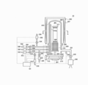
- FIG. 2 is a sectional view taken along line AA in FIG. 1.
- FIG. 1 is a block diagram which shows the structure of the controller which the substrate processing apparatus shown in FIG. 1 has.
- a tungsten (W) film is used as an electrode used for a memory such as a flash memory or a DRAM (Dynamic Random Access Memory), or a metal film used for wiring between the electrodes.
- a method of forming the film a method of forming a film on the substrate by simultaneously supplying (continuously supplying) a plurality of processing gases to the substrate and utilizing a reaction of the plurality of processing gases in the gas phase or on the substrate surface.
- there is a method of forming a film on the substrate by supplying a plurality of processing gases to the substrate in a time-sharing manner (asynchronously, intermittently, in pulses).
- the latter method of supplying a plurality of process gases capable of obtaining better film thickness uniformity in a time-sharing manner is effective.
- the resistivity of the obtained metal film becomes high, usually the former method of supplying a plurality of processing gases at the same time is often used for forming the W film.
- the metal film at the time of embedding may be in an amorphous state. It is desirable that the crystallization temperature of the W film is low, and crystallization occurs at a temperature of about 200 to 250 ° C. when using a method in which a plurality of processing gases are supplied simultaneously.
- the temperature required for this is 500 ° C.
- a W film formed in a very narrow groove with a narrow opening is a W film formed by low-temperature treatment, and has a low roughness, a low resistivity, and a crystallized W film.
- the inventors have conducted intensive research and formed a crystallized W layer on an amorphous W film, and the effect of the crystallized W layer on the amorphous W film is increased. Since the film crystallizes, it was found that as a result, a crystallized W film can be formed on the substrate (reverse solid phase reaction).
- the temperature required for forming the crystallized W layer is 250 ° C. or lower, preferably 200 ° C. or lower. Even when a plurality of processing gases are simultaneously supplied to the substrate at a temperature of about 200 ° C., an amorphous W layer (A) is formed up to a certain thickness (a). I found out that I can do it.
- an amorphous W layer (B) is sandwiched between amorphous W layers (A) (amorphous W layer (A) and amorphous W layer (B) are laminated) It was found that an amorphous W film having a desired film thickness can be formed.
- an amorphous W layer (A) and an amorphous W layer (B) are combined to form an amorphous W film having a desired thickness, and a crystallized W layer is formed thereon.
- a W film crystallized with a low roughness and a low resistivity can be formed in an ultrafine groove with a narrow opening by a low temperature treatment of 200 ° C. or lower. Details will be described below.
- the substrate processing apparatus 10 is configured as an example of an apparatus used in a substrate processing process, which is a process of manufacturing a semiconductor device (device).
- the processing furnace 202 is provided with a heater 207 as a heating means (heating mechanism, heating system).
- the heater 207 is formed in a cylindrical shape whose upper side is closed.
- reaction tube 203 constituting a reaction vessel (processing vessel) concentrically with the heater 207 is disposed.
- the reaction tube 203 is made of a heat-resistant material or the like (for example, quartz (SiO 2 ) or silicon carbide (SiC)), and is formed in a cylindrical shape with the upper end closed and the lower end opened.
- a manifold 209 made of a metal material such as stainless steel is attached to the lower end of the reaction tube 203.
- the manifold 209 is formed in a cylindrical shape, and its lower end opening is airtightly closed by a seal cap 219 as a lid made of a metal material such as stainless steel.
- An O-ring 220 as a seal member is provided between the reaction tube 203 and the manifold 209 and between the manifold 209 and the seal cap 219, respectively.
- a processing container is mainly constituted by the reaction tube 203, the manifold 209, and the seal cap 219, and a processing chamber 201 is formed inside the processing container.
- the processing chamber 201 is configured so that wafers 200 as substrates can be accommodated by a boat 217, which will be described later, in a horizontal posture and arranged in multiple stages in the vertical direction.
- a rotation mechanism 267 that rotates the boat 217 is installed on the side of the seal cap 219 opposite to the processing chamber 201.
- a rotation shaft 255 of the rotation mechanism 267 passes through the seal cap 219 and is connected to the boat 217.
- the rotation mechanism 267 is configured to rotate the wafer 200 by rotating the boat 217.
- the seal cap 219 is configured to be lifted and lowered in the vertical direction by a boat elevator 115 as a lifting mechanism vertically installed outside the reaction tube 203.
- the boat elevator 115 is configured so that the boat 217 can be carried in and out of the processing chamber 201 by moving the seal cap 219 up and down. That is, the boat elevator 115 is configured as a transfer device (transfer mechanism) that transfers the boat 217, that is, the wafers 200 into and out of the processing chamber 201.
- the boat 217 serving as a substrate holder is configured to support a plurality of, for example, 25 to 200 wafers 200 in a horizontal posture and in a multi-stage by aligning them in the vertical direction with their centers aligned. Are arranged so as to be spaced apart.
- the boat 217 is made of a heat resistant material or the like (for example, quartz or SiC).
- heat insulating plates 218 made of a heat-resistant material or the like (for example, quartz or SiC) are supported in multiple stages in a horizontal posture. With this configuration, heat from the heater 207 is not easily transmitted to the seal cap 219 side.
- this embodiment is not limited to the above-mentioned form.
- a heat insulating cylinder configured as a cylindrical member made of a heat resistant material such as quartz or SiC may be provided.
- the heater 207 can heat the wafer 200 accommodated in the processing chamber 201 to a predetermined temperature.
- nozzles 410, 420, and 430 are provided so as to penetrate the side wall of the manifold 209.
- Gas supply pipes 310, 320, and 330 as gas supply lines are connected to the nozzles 410, 420, and 430, respectively.
- the processing furnace 202 is provided with the three nozzles 410, 420, and 430 and the three gas supply pipes 310, 320, and 330.
- the gas (processing gas) can be supplied through a dedicated line.
- the gas supply pipes 310, 320, and 330 are provided with mass flow controllers (MFCs) 312, 322, 332 that are flow rate controllers (flow rate control units), and valves 314, 324, and 334 that are on-off valves in order from the upstream side. ing.
- MFCs mass flow controllers
- Nozzles 410, 420, and 430 are connected (connected) to the distal ends of the gas supply pipes 310, 320, and 330, respectively.
- the nozzles 410, 420, and 430 are configured as L-shaped long nozzles, and the horizontal portion thereof is provided so as to penetrate the side wall of the manifold 209.
- the vertical portions of the nozzles 410, 420, and 430 are in an annular space formed between the inner wall of the reaction tube 203 and the wafer 200, and upward (upward in the stacking direction of the wafer 200) along the inner wall of the reaction tube 203. It is provided so as to rise upward (that is, so as to rise from one end side to the other end side of the wafer arrangement region). That is, the nozzles 410, 420, and 430 are provided along the wafer arrangement region in a region that horizontally surrounds the wafer arrangement region on the side of the wafer arrangement region where the wafers 200 are arranged.
- Gas supply holes 410a, 420a, and 430a for supplying (spouting) gas are provided on the side surfaces of the nozzles 410, 420, and 430, respectively.
- the gas supply holes 410a, 420a, and 430a are opened to face the center of the reaction tube 203, respectively.
- a plurality of the gas supply holes 410a, 420a, 430a are provided from the lower part to the upper part of the reaction tube 203, have the same opening area, and are provided at the same opening pitch.
- the gas supply method according to the present embodiment is an annular vertically long space defined by the inner wall of the reaction tube 203 and the ends of the stacked wafers 200, that is, a cylindrical shape.
- Gas is transferred via nozzles 410, 420, and 430 disposed in the space, and is first in the reaction tube 203 from the gas supply holes 410 a, 420 a, and 430 a opened in the nozzles 410, 420, and 430, respectively, in the vicinity of the wafer 200.
- the main flow of gas in the reaction tube 203 is in a direction parallel to the surface of the wafer 200, that is, in the horizontal direction.
- a gas flowing on the surface of each wafer 200 that is, a gas remaining after the reaction (residual gas) flows toward an exhaust port, that is, an exhaust pipe 231 to be described later.
- the direction is appropriately specified depending on the position of the exhaust port, and is not limited to the vertical direction.
- carrier gas supply pipes 510, 520, and 530 for supplying a carrier gas are connected to the gas supply pipes 310, 320, and 330, respectively.
- Carrier gas supply pipes 510, 520, and 530 are provided with MFCs 512, 522, and 532 and valves 514, 524, and 534, respectively.
- a raw material gas containing a metal element (metal-containing raw material, metal-containing gas, metal raw material) is supplied from the gas supply pipe 310 as a processing gas via the MFC 312, the valve 314, and the nozzle 410. Supplied in.
- the source gas for example, tungsten hexafluoride (WF 6 ) gas that is a W-containing source gas containing tungsten (W) as a metal element is used.
- WF 6 gas acts as a W source in a substrate processing step described later.
- a second reducing gas having an action of reducing the source gas is supplied as a processing gas into the processing chamber 201 through the MFC 322, the valve 324, and the nozzle 420.
- an H-containing gas containing hydrogen (H) for example, hydrogen (H 2 ) is used.
- H 2 gas acts as an H source in a substrate processing step described later.
- a first reducing gas having a function of reducing the source gas is supplied as a processing gas into the processing chamber 201 through the MFC 332, the valve 334, and the nozzle 430.
- a B-containing gas containing boron (B), for example, diborane (B 2 H 6 ) is used as the first reducing gas.
- B 2 H 6 gas acts as a B source in a substrate processing step to be described later.
- nitrogen (N 2 ) gas as an inert gas is processed through MFCs 512, 522, 532, valves 514, 524, 534, and nozzles 410, 420, 430, respectively. It is supplied into the chamber 201.
- the processing gas, the raw material gas, and the reducing gas are vaporized raw materials and reducing agents, for example, raw materials and reducing agents that are in a liquid state or a solid state at room temperature and normal pressure. Or a raw material or a reducing agent that is in a gaseous state at normal temperature and pressure.
- raw material when used, it means “liquid raw material in a liquid state”, “solid raw material in a solid state”, “source gas in a gaseous state”, or a combination thereof.
- reducing agent a liquid reducing agent in a liquid state
- a solid reducing agent in a solid state a reducing gas in a gaseous state
- a combination thereof May mean.
- liquid raw materials that are in a liquid state at room temperature and normal pressure, or solid raw materials that are in a solid state at normal temperature and pressure vaporize or sublimate the liquid raw material or solid raw material with a system such as a vaporizer, bubbler, or sublimator.
- a system such as a vaporizer, bubbler, or sublimator.
- a processing gas supply system is mainly configured by the gas supply pipes 310, 320, 330, MFCs 312, 322, 332, and valves 314, 324, and 334. Is done.
- the nozzles 410, 420, and 430 may be included in the processing gas supply system.
- the processing gas supply system can be simply referred to as a gas supply system.
- a raw material gas supply system is mainly configured by the gas supply pipe 310, the MFC 312 and the valve 314.
- the nozzle 410 may be included in the source gas supply system.
- the source gas supply system can also be referred to as a source supply system.
- a W-containing gas supply system is mainly configured by the gas supply pipe 310, the MFC 312 and the valve 314.
- the nozzle 410 may be included in the W-containing gas supply system.
- the W-containing gas supply system can be referred to as a W-containing raw material supply system, or can be simply referred to as a W raw material supply system.
- W-containing gas supply system When flowing WF 6 gas from the gas supply pipe 310, it may also be referred to as the W-containing gas supply system and the WF 6 gas supply system.
- the WF 6 gas supply system can also be referred to as a WF 6 supply system.
- a reducing gas supply system is mainly configured by the gas supply pipes 320 and 330, the MFCs 322 and 332, and the valves 324 and 334.
- the nozzles 420 and 430 may be included in the reducing gas supply system.
- the reducing gas supply system can also be referred to as a reducing agent supply system.
- an H-containing gas supply system is mainly configured by the gas supply pipe 320, the MFC 322, and the valve 324.
- the nozzle 420 may be included in the H-containing gas supply system.
- H-containing gas supply system When flowing H 2 gas from the gas supply pipe 320, it may also be referred to as the H-containing gas supply system and the H 2 gas supply system.
- the H 2 gas supply system can also be referred to as an H 2 supply system.
- a B-containing gas supply system is mainly configured by the gas supply pipe 330, the MFC 332, and the valve 334.
- the nozzle 430 may be included in the B-containing gas supply system.
- the B-containing gas supply system can also be referred to as a B-containing reducing gas supply system, and can also be referred to as a B-containing reducing agent supply system. If flow B 2 H 6 gas from the gas supply pipe 330, may also be referred to as a B-containing gas supply system and B 2 H 6 gas supply system.
- the B 2 H 6 gas supply system can also be referred to as a B 2 H 6 supply system.
- a carrier gas supply system is mainly configured by the carrier gas supply pipes 510, 520, 530, MFCs 512, 522, 532, valves 514, 524, 534.
- the carrier gas supply system can also be referred to as an inert gas supply system. Since this inert gas also acts as a purge gas, the inert gas supply system can also be referred to as a purge gas supply system.
- the manifold 209 is provided with an exhaust pipe 231 for exhausting the atmosphere in the processing chamber 201.
- the exhaust pipe 231 is provided so as to penetrate the side wall of the manifold 209, similarly to the nozzles 410, 420, and 430. As shown in FIG. 2, the exhaust pipe 231 is provided at a position facing the nozzles 410, 420, and 430 across the wafer 200 in plan view.
- the gas supplied from the gas supply holes 410a, 420a, and 430a to the vicinity of the wafer 200 in the processing chamber 201 flows in the horizontal direction, that is, in the direction parallel to the surface of the wafer 200 and then downward. Then, the air flows through the exhaust pipe 231.
- the main flow of gas in the processing chamber 201 is a flow in the horizontal direction.
- the exhaust pipe 231 includes, in order from the upstream side, a pressure sensor 245 as a pressure detector (pressure detector) that detects the pressure in the processing chamber 201, and a pressure controller (pressure controller) that controls the pressure in the processing chamber 201.
- a pressure sensor 245 as a pressure detector (pressure detector) that detects the pressure in the processing chamber 201
- a pressure controller pressure controller
- the APC valve 243 can open and close the vacuum pump 246 while the vacuum pump 246 is operated, thereby performing vacuum exhaust and stop the vacuum exhaust in the processing chamber 201. Further, with the vacuum pump 246 operated, The pressure in the processing chamber 201 can be adjusted by adjusting the valve opening based on the pressure information detected by the pressure sensor 245.
- the APC valve 243 constitutes a part of the exhaust flow path of the exhaust system, and not only functions as a pressure adjusting unit, but also closes or further seals the exhaust flow path of the exhaust system. It also functions as a possible exhaust flow path opening / closing part, that is, an exhaust valve.
- the exhaust pipe 231 has a trap device that captures reaction by-products and unreacted source gas in the exhaust gas, and a detoxification device that removes corrosive components and toxic components contained in the exhaust gas. May be connected.
- An exhaust system, that is, an exhaust line, is mainly configured by the exhaust pipe 231, the APC valve 243, and the pressure sensor 245.
- the vacuum pump 246 may be included in the exhaust system.
- a trap device or a detoxifying device may be included in the exhaust system.
- a temperature sensor 263 as a temperature detector is installed in the reaction tube 203, and the temperature in the processing chamber 201 is adjusted by adjusting the energization amount to the heater 207 based on the temperature information detected by the temperature sensor 263. It is configured to have a desired temperature distribution.
- the temperature sensor 263 is configured in an L shape like the nozzles 410, 420, and 430, and is provided along the inner wall of the reaction tube 203.
- the controller 121 which is a control unit (control means), is configured as a computer including a CPU (Central Processing Unit) 121a, a RAM (Random Access Memory) 121b, a storage device 121c, and an I / O port 121d. ing.
- the RAM 121b, the storage device 121c, and the I / O port 121d are configured to exchange data with the CPU 121a via the internal bus 121e.
- An input / output device 122 configured as a touch panel or the like is connected to the controller 121.
- the storage device 121c includes a flash memory, an HDD (HardDisk Drive), and the like.
- a control program that controls the operation of the substrate processing apparatus, a process recipe that describes the procedure and conditions of the substrate processing described later, and the like are stored in a readable manner.
- the process recipe is a combination of instructions so that the controller 121 can execute each procedure in the substrate processing process described later and obtain a predetermined result, and functions as a program.
- the process recipe, the control program, and the like are collectively referred to as simply a program.
- program When the term “program” is used in this specification, it may include only a process recipe alone, only a control program alone, or both.
- the RAM 121b is configured as a memory area (work area) in which programs, data, and the like read by the CPU 121a are temporarily stored.
- the I / O port 121d includes the above-described MFC 312, 322, 332, 512, 522, 532, valve 314, 324, 334, 514, 524, 534, APC valve 243, pressure sensor 245, vacuum pump 246, heater 207, temperature The sensor 263, the rotation mechanism 267, the boat elevator 115 and the like are connected.
- the CPU 121a is configured to read and execute a control program from the storage device 121c, and to read a process recipe from the storage device 121c in response to an operation command input from the input / output device 122 or the like.
- the CPU 121a adjusts the flow rates of various gases by the MFCs 312, 322, 332, 512, 522, and 532, opens and closes the valves 314, 324, 334, 514, 524, and 534, and opens and closes the APC valve 243.
- boat elevator 115 is configured to control the lifting and lowering operation of the boat 217 by 115.
- the controller 121 is not limited to being configured as a dedicated computer, and may be configured as a general-purpose computer.
- an external storage device storing the above-described program for example, magnetic tape, magnetic disk such as a flexible disk or hard disk, optical disk such as CD or DVD, magneto-optical disk such as MO, semiconductor memory such as USB memory or memory card
- the controller 121 of this embodiment can be configured by installing a program in a general-purpose computer using the external storage device 123.
- the means for supplying the program to the computer is not limited to supplying the program via the external storage device 123.
- the program may be supplied without using the external storage device 123 by using communication means such as the Internet or a dedicated line.
- the storage device 121c and the external storage device 123 are configured as computer-readable recording media. Hereinafter, these are collectively referred to simply as a recording medium.
- recording medium When the term “recording medium” is used in this specification, it may include only the storage device 121c alone, may include only the external storage device 123 alone, or may include both.
- Substrate processing step As an example of a semiconductor device (device) manufacturing step, an example of a step of forming a metal film constituting a gate electrode on a substrate will be described with reference to FIGS. 4, 5, and 6. explain.
- the step of forming the metal film is performed using the processing furnace 202 of the substrate processing apparatus 10 described above. In the following description, the operation of each part constituting the substrate processing apparatus 10 is controlled by the controller 121.
- FIG. 4 shows an example of a stack structure to which this embodiment is applied.
- a titanium nitride film (TiN film) 502 is formed as a barrier metal film on a silicon oxide film (SiO 2 film) 501, and a tungsten film (W film) is formed as a seed layer on the TiN film 502. ) 503, and, for example, amorphous tungsten layers (amorphous W layer, ⁇ -W layer) 504 and 505 are alternately stacked on the W film 503 as a bulk layer.
- TiN film titanium nitride film
- SiO 2 film silicon oxide film
- W film tungsten film
- a metal-containing gas for example, WF 6 gas
- a first reducing gas for example, H 2 gas
- a second amorphous metal layer for example, a W layer
- a metal-containing gas on the wafer 200 on which the amorphous metal film is formed.
- the first reducing gas are simultaneously supplied to form amorphous gold formed on the wafer 200 Forming a crystallized metal layer on a film (e.g., a W layer), it is carried out.
- WF 6 gas and H 2 gas are supplied simultaneously to form a first amorphous W layer (also referred to as an amorphous W layer or an ⁇ -W layer).
- steps and, WF 6 gas and B 2 H 6 a predetermined number of times by time division and gas (n 1 times) is supplied, the step of forming a second alpha-W layer over the first alpha-W layer And performing a predetermined number of times (n 2 times) in a time-sharing manner to form an amorphous W film (also referred to as an amorphous W film or an ⁇ -W film) on the wafer 200, WF 6 gas and H 2 Gas is simultaneously supplied to form a crystallized W layer on the ⁇ -W film.
- processing or process, cycle, step, etc. is performed a predetermined number of times” means that this processing or the like is performed once or a plurality of times. That is, it means that the process is performed once or more.
- FIG. 5 shows an example in which each process (cycle) is repeated alternately for n 1 cycles and n 2 cycles.
- the value of n 1 is appropriately selected according to the film thickness of the second ⁇ -W layer that is required so that the first ⁇ -W layer to be formed next does not crystallize.
- the value of n 2 is appropriately selected according to the film thickness required for the finally formed ⁇ -W film.
- time division means that the time division (separation) is performed.
- performing each process in a time-sharing manner means that each process is performed asynchronously, that is, without being synchronized.
- each process is performed intermittently (pulse-like) and alternately. That is, it means that the processing gases supplied in each process are supplied so as not to mix with each other.
- the process gases supplied in each process are alternately supplied so as not to mix with each other.
- wafer when the term “wafer” is used in this specification, it means “wafer itself” or “a laminate (aggregate) of a wafer and a predetermined layer or film formed on the surface thereof”. ", That is, a predetermined layer or film formed on the surface may be referred to as a wafer.
- wafer surface when the term “wafer surface” is used in this specification, it means “the surface of the wafer itself (exposed surface)” or “the surface of a predetermined layer or film formed on the wafer”. That is, it may mean “the outermost surface of the wafer as a laminated body”.
- the phrase “supplying a predetermined gas to the wafer” means “supplying a predetermined gas directly to the surface (exposed surface) of the wafer itself”. , It may mean that “a predetermined gas is supplied to a layer, a film, or the like formed on the wafer, that is, to the outermost surface of the wafer as a laminated body”. Further, in this specification, when “describe a predetermined layer (or film) on the wafer” is described, “determine a predetermined layer (or film) directly on the surface (exposed surface) of the wafer itself”. This means that a predetermined layer (or film) is formed on a layer or film formed on the wafer, that is, on the outermost surface of the wafer as a laminate. There is a case.
- substrate in this specification is the same as the term “wafer”. In that case, in the above description, “wafer” is replaced with “substrate”. Good.
- metal film means a film composed of a conductive substance containing metal atoms (also simply referred to as a conductor film), which mainly includes metal atoms.
- the W film is a conductive metal film and is a single metal film.
- amorphous film (or layer) means that the main component constituting the corresponding film (layer) is not crystallized.
- film (or layer) means that the main component constituting the corresponding film (layer) is crystallized (crystalline). Therefore, the term “amorphous film (or layer)” may contain a crystallized component that does not become a main component, or the term “crystallized film (or layer)”. May contain an amorphous component to the extent that it does not become the main component. Further, when ⁇ or a is added to the film type name or the like, it indicates that the film is amorphous.
- the inside of the processing chamber 201 is evacuated by a vacuum pump 246 so that a desired pressure (degree of vacuum) is obtained.
- a desired pressure degree of vacuum
- the vacuum pump 246 keeps operating at least until the processing on the wafer 200 is completed.
- the wafer 200 in the processing chamber 201 is heated by the heater 207 so as to reach a desired temperature.
- the energization amount to the heater 207 is feedback-controlled based on the temperature information detected by the temperature sensor 263 so that the processing chamber 201 has a desired temperature distribution (temperature adjustment).
- the heating of the processing chamber 201 by the heater 207 is continuously performed at least until the processing on the wafer 200 is completed.
- the rotation mechanism 267 starts the rotation of the boat 217 and the wafer 200. Note that the rotation of the boat 217 and the wafer 200 by the rotation mechanism 267 is continuously performed at least until the processing on the wafer 200 is completed.
- the ⁇ -W film forming step includes a first ⁇ -W layer forming step for forming a first ⁇ -W layer as an ⁇ -W layer 504 and a second ⁇ -W layer 505 as described below. a second ⁇ -W layer forming step of forming an ⁇ -W layer.
- the first ⁇ -W layer forming step includes a WF 6 gas and H 2 gas supply step and a residual gas removal step described below.
- the flow rate of the WF 6 gas that has flowed through the gas supply pipe 310 and the H 2 gas that has flowed through the gas supply pipe 320 are adjusted by the MFCs 312 and 322, respectively, and are respectively supplied from the gas supply holes 410 a and 420 a of the nozzles 410 and 420. Is exhausted from the exhaust pipe 231.
- WF 6 gas and H 2 gas are supplied to the wafer 200. That is, the surface of the wafer 200 is exposed to WF 6 gas and H 2 gas.
- the valves 514 and 524 are opened, and N 2 gas is caused to flow into the carrier gas supply pipes 510 and 520, respectively.
- the N 2 gas flowing through the carrier gas supply pipes 510 and 520 is adjusted in flow rate by the MFCs 512 and 522, supplied to the processing chamber 201 together with the WF 6 gas or H 2 gas, and exhausted from the exhaust pipe 231.
- the valve 534 is opened and the N 2 gas is allowed to flow into the carrier gas supply pipe 530.
- the N 2 gas is supplied into the processing chamber 201 through the gas supply pipe 330 and the nozzle 430 and is exhausted from the exhaust pipe 231.
- the APC valve 243 is appropriately adjusted so that the pressure in the processing chamber 201 is, for example, a pressure within a range of 10 to 1300 Pa, for example, 70 Pa.
- the supply flow rate of WF 6 gas controlled by the MFC 312 is, for example, a flow rate in the range of 10 to 1000 sccm, for example, 100 sccm
- the supply flow rate of H 2 gas controlled by the MFC 322 is, for example, a flow rate in the range of 100 to 20000 sccm. For example, 10000 sccm.
- the supply flow rate of the N 2 gas controlled by the MFCs 512, 522, and 532 is, for example, a flow rate in the range of 10 to 10,000 sccm, for example, 5000 sccm.
- the time for supplying the WF 6 gas and the H 2 gas to the wafer 200 is, for example, a time within the range of 1 to 1000 seconds.
- the temperature of the heater 207 is such that the temperature of the wafer 200 becomes a temperature within the range of room temperature to 250 ° C., for example, and preferably within the range of 150 to 230 ° C. Set to ° C.
- the temperature of the wafer 200 When the temperature of the wafer 200 is lower than room temperature, there is an impediment that the reaction energy for forming the film is insufficient and there is a high possibility that the film is not formed. Further, when the temperature of the wafer 200 is higher than 250 ° C., it will be B 2 H 6 gas supplied by B 2 H 6 gas supply step of the second alpha-W layer formed step is deposition B by autolysis, There is a high possibility that it will be an obstacle to film formation.
- the WF 6 gas and the H 2 gas flowing in the processing chamber 201 react in the gas phase (gas phase reaction) or react on the substrate surface, and on the wafer 200 (the underlying film on the surface, for example, the seed layer 503), A first ⁇ -W layer is formed.
- the ⁇ -W layer is a continuous layer composed of amorphous W, a discontinuous layer, or an amorphous W layer formed by overlapping these layers. sometimes it contains F included in the WF 6 molecules are.
- the process conditions such as the supply flow rate and supply time of WF 6 gas and H 2 gas, the ⁇ -W layer can be grown to a desired film thickness.
- the crystallization of the film depends on the thickness of the film. Therefore, in the first ⁇ -W layer formation step, the supply of the WF 6 gas and the H 2 gas is stopped before the W film reaches a film thickness where crystallization occurs.
- the film thickness at which crystallization does not occur is preferably greater than 0 nm and 3 nm or less. Preferably, it is 0.1 nm or more and 3 nm or less.
- the valves 314 and 324 are closed, and the supply of the WF 6 gas and the H 2 gas is stopped.
- the APC valve 243 is kept open, the processing chamber 201 is evacuated by the vacuum pump 246, and the processing chamber 201 (that is, the space where the wafer 200 on which the first ⁇ -W layer is formed) exists.
- the WF 6 gas and the H 2 gas remaining in the substrate and contributing to the formation of the first ⁇ -W layer are excluded from the processing chamber 201.
- the valves 514, 524, and 534 remain open, and the supply of N 2 gas into the processing chamber 201 is maintained.
- the N 2 gas acts as a purge gas, and has the effect of removing unreacted WF 6 gas and H 2 gas remaining in the processing chamber 201 or contributing to the formation of the first ⁇ -W layer from the processing chamber 201. Can be increased. At this time, if a by-product is generated in the processing chamber 201 by the first ⁇ -W layer forming step, this by-product is also excluded from the processing chamber 201.
- the gas remaining in the processing chamber 201 may not be completely removed, and the inside of the processing chamber 201 may not be completely purged.
- a trace amount of gas may remain in the processing chamber 201 as long as there is no adverse effect in subsequent steps.
- the flow rate of the N 2 gas supplied into the processing chamber 201 does not need to be a large flow rate.
- Purge can be performed to the extent that no adverse effect occurs in the subsequent steps.
- the purge time can be shortened and the throughput can be improved.
- consumption of N 2 gas can be minimized.
- the second ⁇ -W layer forming step includes a WF 6 gas supply step, a residual gas removal step, a B 2 H 6 gas supply step, and a residual gas supply step described below.
- the valve 314 is opened and WF 6 gas is allowed to flow into the gas supply pipe 310.
- the flow rate of the WF 6 gas flowing through the gas supply pipe 310 is adjusted by the MFC 312, supplied from the gas supply hole 410 a of the nozzle 410 into the processing chamber 201, and exhausted from the exhaust pipe 231.
- WF 6 gas is supplied to the wafer 200. That is, the surface of the wafer 200 is exposed to WF 6 gas.
- the valve 514 is opened and N 2 gas is allowed to flow into the carrier gas supply pipe 510.
- the N 2 gas that has flowed through the carrier gas supply pipe 510 is adjusted in flow rate by the MFC 512, supplied into the processing chamber 201 together with the WF 6 gas, and exhausted from the exhaust pipe 231.
- the valves 524 and 534 are opened, and the N 2 gas is caused to flow into the carrier gas supply pipes 520 and 530.
- the N 2 gas is supplied into the processing chamber 201 through the gas supply pipes 320 and 330 and the nozzles 420 and 430 and is exhausted from the exhaust pipe 231.
- the APC valve 243 is appropriately adjusted so that the pressure in the processing chamber 201 is, for example, a pressure within a range of 10 to 1300 Pa, for example, 70 Pa.
- the supply flow rate of the WF 6 gas controlled by the MFC 312 is, for example, a flow rate in the range of 10 to 1000 sccm, for example, 100 sccm.
- the supply flow rate of the N 2 gas controlled by the MFCs 512, 522, and 532 is, for example, a flow rate in the range of 10 to 10,000 sccm, for example, 5000 sccm.
- the time for supplying the WF 6 gas to the wafer 200 is, for example, a time within the range of 0.1 to 50 seconds.
- the temperature of the heater 207 is set to the same temperature as in the first ⁇ -W layer forming step.
- the gases flowing into the processing chamber 201 are only WF 6 gas and N 2 gas.
- the ⁇ -W-containing layer is ideally desirably an ⁇ -W layer, but the ⁇ -W (F) layer may be the main element.
- the ⁇ -W layer includes a discontinuous layer as well as a continuous layer composed of ⁇ -W. That is, the ⁇ -W layer includes a W deposition layer having a thickness of less than one atomic layer to several atomic layers constituted by ⁇ -W.
- the ⁇ -W (F) layer is a W-containing layer containing F, and may be an ⁇ -W layer containing F or an adsorption layer of WF 6 .
- the main element is the ⁇ -W (F) layer
- the reduction reaction by the B 2 H 6 gas supply step described later is particularly effective.
- the W layer containing F is a generic name including a discontinuous layer formed of W, a discontinuous layer, and a W thin film containing F formed by overlapping them.
- a continuous layer composed of W and containing F may be referred to as a W thin film containing F.
- W constituting the W layer containing F includes not only completely broken bond with F but also completely broken bond with F.
- WF 6 molecules constituting the adsorption layer of WF 6 include those in which the bond between W and F is partially broken. That is, the adsorption layer of WF 6 may be a physical adsorption layer of WF 6 may be a chemical adsorption layer of WF 6, may contain both.
- a layer having a thickness of less than one atomic layer means an atomic layer formed discontinuously, and a layer having a thickness of one atomic layer means an atomic layer formed continuously.
- a layer having a thickness of less than one molecular layer means a molecular layer formed discontinuously, and a layer having a thickness of one molecular layer means a molecular layer formed continuously.
- the ⁇ -W-containing layer can include both a W layer containing F and an adsorption layer of WF 6 . However, as described above, the ⁇ -W-containing layer is expressed using expressions such as “one atomic layer” and “several atomic layer”.
- a W layer containing F is formed by depositing W on the wafer 200.
- the thickness of the W-containing layer exceeds several atomic layers, the reduction action in the B 2 H 6 gas supply step described later does not reach the entire ⁇ -W-containing layer.
- the minimum value of the thickness of the ⁇ -W-containing layer is less than one atomic layer. Therefore, the thickness of the first layer is preferably less than one atomic layer to several atomic layers.
- the time required for forming the ⁇ -W-containing layer in the WF 6 supply step can also be shortened.
- the processing time per cycle can be shortened, and the total processing time can be shortened. That is, the film forming rate can be increased.
- the thickness of the ⁇ -W-containing layer to 1 atomic layer or less, it becomes possible to improve the controllability of the film thickness uniformity.
- the valves 514, 524, and 534 remain open, and the supply of N 2 gas into the processing chamber 201 is maintained.
- the N 2 gas acts as a purge gas, and can enhance the effect of removing the unreacted WF 6 gas remaining in the processing chamber 201 or contributing to the formation of the ⁇ -W-containing layer from the processing chamber 201.
- the gas remaining in the processing chamber 201 may not be completely removed, and the processing chamber 201 may not be completely purged.
- B 2 H 6 Gas Supply Step The valve 334 is opened and B 2 H 6 gas is allowed to flow into the gas supply pipe 330.
- the flow rate of the B 2 H 6 gas flowing through the gas supply pipe 330 is adjusted by the MFC 332, supplied into the processing chamber 201 from the gas supply hole 430 a of the nozzle 430, and exhausted from the exhaust pipe 231.
- B 2 H 6 gas is supplied to the wafer 200. That is, the surface of the wafer 200 is exposed to B 2 H 6 gas.
- the valve 534 is opened, and N 2 gas is caused to flow into the carrier gas supply pipe 530.
- the N 2 gas flowing through the carrier gas supply pipe 530 is adjusted in flow rate by the MFC 532 and supplied into the processing chamber 201 together with the B 2 H 6 gas, and is exhausted from the exhaust pipe 231.
- the valves 514 and 524 are opened, and N 2 gas is allowed to flow into the carrier gas supply pipes 510 and 520.
- the N 2 gas is supplied into the processing chamber 201 through the gas supply pipes 310 and 320 and the nozzles 410 and 420 and is exhausted from the exhaust pipe 231.
- the APC valve 243 is appropriately adjusted so that the pressure in the processing chamber 201 is, for example, a pressure within a range of 10 to 1300 Pa, for example, 70 Pa.
- the supply flow rate of the B 2 H 6 gas controlled by the MFC 332 is, for example, a flow rate in the range of 10 to 20000 sccm, for example, 10,000 sccm.
- the supply flow rate of the N 2 gas controlled by the MFCs 512, 522, and 532 is, for example, a flow rate in the range of 10 to 10,000 sccm, for example, 5000 sccm.
- the time for supplying the B 2 H 6 gas to the wafer 200 is, for example, a time within the range of 0.1 to 60 seconds.
- the temperature of the heater 207 is set to the same temperature as the first ⁇ -W layer forming step and the WF 6 gas supply step.
- the gases flowing into the processing chamber 201 are only B 2 H 6 gas and N 2 gas, and ⁇ -W containing formed on the wafer 200 in the WF 6 gas supply step by supplying B 2 H 6 gas.
- the layer is reduced to form a second ⁇ -W layer.
- H of the B 2 H 6 gas reacts with F contained in the ⁇ -W-containing layer formed in the WF 6 gas supply step to be reduced to hydrogen fluoride (HF).
- HF hydrogen fluoride
- at least a part of boron (B) which is a residual component of the B 2 H 6 gas, may remain in the second ⁇ -W layer as a residue. Therefore, at least a part of the second ⁇ -W layer may be an ⁇ -W (B) layer, that is, an ⁇ -W layer containing B.
- B remains as an impurity in the ⁇ -W layer, so that the formed ⁇ -W (B) layer becomes an amorphous state. Therefore, in that respect, it is preferable that B remains as an impurity in the ⁇ -W layer.
- a cycle in which the WF 6 gas supply step, the residual gas removal step, the B 2 H 6 gas supply step, and the residual gas removal step described above are sequentially time-divisionally (asynchronously, intermittently, and pulsed) is 1 More than once (predetermined number of times), that is, the WF 6 gas supply step, the residual gas removal step, the B 2 H 6 gas supply step, and the residual gas removal step are regarded as one cycle, and these processes are performed for n 1 cycles (n 1 Is performed on the wafer 200, a second ⁇ -W layer having a predetermined thickness (for example, 0.1 to 2.0 nm) is formed.
- the predetermined thickness is such that when the first ⁇ -W layer forming step is performed next, the W layer formed on the second ⁇ -W layer is not crystallized but is amorphous ( The thickness is determined in consideration of a film thickness necessary for forming the first ⁇ -W layer.
- the above steps are preferably repeated multiple times.
- the order of the WF 6 gas supply step and the B 2 H 6 gas supply step may be interchanged. That is, each step may be performed in the order of the B 2 H 6 gas supply step, the residual gas removal step, the WF 6 gas supply step, and the residual gas removal step.
- ⁇ -W having a predetermined thickness configured as a laminated film (nanolaminate film) in which first ⁇ -W layers and second ⁇ -W layers are alternately laminated at the nano level on wafer 200.
- a film is formed. The above steps are preferably repeated multiple times.
- Crystallized W Layer Formation Step Subsequently, a step of forming a crystallized W layer (crystallized W layer) is executed.
- the crystallized W layer formation step includes the same steps as the WF 6 gas and H 2 gas supply step and the residual gas removal step in the first ⁇ -W layer formation step of the ⁇ -W layer formation step.
- the parts different from the first ⁇ -W layer forming step will be described.
- (WF 6 gas and H 2 gas supply step) This step, a WF 6 gas and H 2 gas supply step in the first alpha-W layer forming step, WF 6 gas and H 2 gas supply flow rate and supply time of Change at least one of them.
- the supply flow rate of the WF 6 gas controlled by the MFC 312 is, for example, a flow rate within a range of 10 to 1000 sccm, for example, 100 sccm
- the supply flow rate of the H 2 gas controlled by the MFC 322 is, for example, 10 to 20000 sccm.
- the flow rate is within the range of, for example, 10,000 sccm.
- the supply flow rate of the N 2 gas controlled by the MFCs 512, 522, and 532 is, for example, a flow rate in the range of 10 to 10,000 sccm, for example, 5000 sccm.
- the time for supplying the WF 6 gas and the H 2 gas to the wafer 200, that is, the gas supply time (irradiation time) is, for example, a time within the range of 0.1 to 1000 seconds. In this way, a crystallized W layer is formed on the ⁇ -W film formed on the wafer 200.
- the crystallized W layer is formed by changing at least one of the supply flow rate and supply time of WF 6 gas and H 2 gas.
- the crystallized W layer is a film thicker than 3 nm, and is formed until the ⁇ -W film has a thickness required for crystallization by a (reverse) solid-phase reaction. With such a film thickness, it is considered that the influence of the crystallized W layer extends to the lower ⁇ -W layer and the ⁇ -W layer is gradually crystallized.
- the range of the region affected by crystallization is determined by the film thickness of the formed crystallization W layer.
- the N 2 gas acts as a purge gas, and can enhance the effect of removing the WF 6 gas and the H 2 gas remaining in the processing chamber 201 and contributing to the formation of the crystallized W layer from the processing chamber 201. it can.
- N 2 gas is supplied from each of the gas supply pipes 510, 520, and 530 while the valves 514, 524, and 534 are kept open. Is supplied into the processing chamber 201 and exhausted from the exhaust pipe 231.
- the N 2 gas acts as a purge gas, whereby the inside of the processing chamber 201 is purged with an inert gas, and the gas and by-products remaining in the processing chamber 201 are removed from the processing chamber 201 (purge). Thereafter, the atmosphere in the processing chamber 201 is replaced with an inert gas (inert gas replacement), and the pressure in the processing chamber 201 is returned to normal pressure (return to atmospheric pressure).
- the film when a film is formed by simultaneously supplying a plurality of process gases to the substrate, the film grows in an amorphous state up to a certain film thickness (amorphous W film ( A) as the first ⁇ -W layer), when crystallization occurs when a certain film thickness is exceeded, and when forming a layer by supplying a plurality of processing gases to the substrate in a time-sharing manner,
- the first ⁇ -W layer is based on the fact that the formed layer is in an amorphous state due to the remaining impurities (second ⁇ -W layer as the amorphous W film (B)).
- the second ⁇ -W layer are combined to form an ⁇ -W film as an amorphous W film having a desired film thickness, and a low-temperature treatment at 250 ° C. or less, preferably 200 ° C. or less.
- An ⁇ -W film can be formed.
- a plurality of processing gases are simultaneously supplied to the substrate on the ⁇ -W film to form a film having a thickness greater than a certain thickness, thereby forming a crystallized W layer.
- a W film crystallized by low temperature treatment at a temperature of 250 ° C. or lower, preferably 200 ° C. or lower, having a low roughness and a low resistivity can be applied to at least a part of the film. Can be formed with a good embedding property in an extremely narrow groove.
- an ⁇ -W film is formed by combining a first ⁇ -W layer and a second ⁇ -W layer as a bulk layer, and a crystal is formed thereon.
- a crystallized W film having a desired film thickness is formed by low-temperature treatment at 250 ° C. or lower, preferably 200 ° C. or lower, by forming a formed W layer has been described.
- a tungsten film (W film) 503 is formed as a seed layer formed on a TiN film 502 formed as a barrier metal film as a base of the bulk layer described above will be described with reference to FIG. To do. Detailed description of the same parts as those of the first embodiment will be omitted, and parts different from those of the first embodiment will be described below.
- the W film (seed W film) as a seed layer is a WF 6 gas supply step, residual gas removal, as in the second ⁇ -W layer formation step described in the first embodiment. It is formed by executing a seed W film formation step including a step, a B 2 H 6 gas supply step, and a residual gas supply step. Since the process conditions in each step are the same as those in the second ⁇ -W layer forming step, a description thereof will be omitted.
- the WF 6 gas supply step, residual gas removal step, B 2 H 6 gas supply step, and residual gas removal step are sequentially performed in a time-sharing manner (asynchronously, intermittently, pulsed) at least once (predetermined number of times). That is, the WF 6 gas supply step, the residual gas removal step, the B 2 H 6 gas supply step, and the residual gas removal step are regarded as one cycle, and these processes are performed only for n 3 cycles (n 3 is an integer of 1 or more). By executing this, a seed W film having a predetermined thickness (for example, 0.1 to 3 nm) is formed on the wafer 200. Note that the order of the WF 6 gas supply step and the B 2 H 6 gas supply step may be interchanged as in the second ⁇ -W film formation step.
- each step may be performed in the order of the B 2 H 6 gas supply step, the residual gas removal step, the WF 6 gas supply step, and the residual gas removal step.
- the gas that first contacts the TiN film 502 formed as the barrier metal film is B 2 H 6 gas, it is considered that damage to the TiN film can be reduced as compared with the case where the WF 6 gas contacts first. It is done.
- a flat bulk film can be formed on the entire surface of the wafer 200, and the resistance of the bulk layer can be reduced.
- crystallization can be suppressed by forming a film by supplying a plurality of processing gases in a time-sharing manner, and a further flat tungsten film can be formed.
- the present invention is not limited to the above-described embodiment, and when a film is formed by simultaneously supplying a plurality of processing gases in a low temperature region of room temperature to 250 ° C. (preferably 200 ° C. or less), the film thickness is a certain level or more. In this case, the film is crystallized, and when a film is formed by supplying a plurality of gases in a time-sharing manner, it is effective in forming a film having such a property that it does not crystallize (is amorphous).
- metal nitride films metal nitride films
- metal carbide films metal carbides
- copper (Cu) containing metal elements such as W, titanium (Ti), tantalum (Ta), molybdenum (Mo), and zinc (Zn).
- the present invention can be suitably applied to the formation of metal films such as ruthenium (Ru) and aluminum (Al), and films combining these.
- applicable metal nitride film and metal carbide film include WN film, TiN film, TaN film, MoN film, ZnN film, WC film, TiC film, TaC film, MoC film, ZnC film, WCN film, TiCN film And metal nitride films such as TaCN film, MoCN film, and ZnCN film, metal carbide films, Cu films, Ru films, Al films such as Al films, and films that combine these.
- WF 6 tungsten hexachloride
- TiF 4 titanium tetrafluoride
- TiCl 4 titanium tetrachloride
- tantalum pentachloride (TaCl 5 ) molybdenum pentafluoride (MoF 5 ), molybdenum pentachloride (MoCl 5 ), zinc dich
- B 2 H 6 gas is used as the B-containing gas as the reducing gas.
- monosilane (SiH 4 ) gas or disilane is used as the silicon-containing gas (silane-based gas). It is also possible to use (Si 2 H 6 ) gas or the like.
- deuterium (D 2 ) gas which is an H-containing gas not containing other elements, can be used as the H-containing gas as the reducing gas.
- a rare gas such as argon (Ar) gas, helium (He) gas, neon (Ne) gas, xenon (Xe) gas may be used.
- each modification, each application, and the like can be used in appropriate combination.
- the processing conditions at this time can be set to the same processing conditions as in the above-described embodiment, for example.
- the process recipes are the contents of the substrate processing (film type, composition ratio, film quality, film thickness, processing procedure, processing of the thin film to be formed) It is preferable to prepare individually (multiple preparations) according to the conditions. And when starting a substrate processing, it is preferable to select a suitable process recipe suitably from several process recipes according to the content of a substrate processing.
- the substrate processing apparatus includes a plurality of process recipes individually prepared according to the contents of the substrate processing via an electric communication line or a recording medium (external storage device 123) on which the process recipe is recorded. It is preferable to store (install) in the storage device 121c in advance.
- the CPU 121a included in the substrate processing apparatus When starting the substrate processing, the CPU 121a included in the substrate processing apparatus appropriately selects an appropriate process recipe from a plurality of process recipes stored in the storage device 121c according to the content of the substrate processing. Is preferred. With this configuration, thin films with various film types, composition ratios, film qualities, and film thicknesses can be formed for general use with good reproducibility using a single substrate processing apparatus. In addition, it is possible to reduce the operation burden on the operator (such as an input burden on the processing procedure and processing conditions), and to quickly start the substrate processing while avoiding an operation error.
- the above-described process recipe is not limited to the case of creating a new process, and can be realized by changing the process recipe of an existing substrate processing apparatus, for example.
- the process recipe according to the present invention is installed in an existing substrate processing apparatus via a telecommunication line or a recording medium recording the process recipe, or input / output of the existing substrate processing apparatus It is also possible to operate the apparatus and change the process recipe itself to the process recipe according to the present invention.
- the substrate processing apparatus is a batch type vertical apparatus that processes a plurality of substrates at a time, and a nozzle for supplying a processing gas is erected in one reaction tube.
- a processing furnace having a structure in which an exhaust port is provided in the lower part has been described
- the present invention can also be applied to a case where a film is formed using a processing furnace having another structure.
- there are two reaction tubes having a concentric cross section the outer reaction tube is called an outer tube and the inner reaction tube is called an inner tube), and a side wall of the outer tube is provided from a nozzle standing in the inner tube.
- the present invention can also be applied to a case where a film is formed using a processing furnace having a structure in which a processing gas flows to an exhaust port that opens to a position (axisymmetric position) facing the nozzle with the substrate interposed therebetween.
- the processing gas may be supplied from a gas supply port that opens in a side wall of the inner tube, instead of being supplied from a nozzle standing in the inner tube.
- the exhaust port opened to the outer tube may be opened according to the height at which there are a plurality of substrates stacked and accommodated in the processing chamber.
- the shape of the exhaust port may be a hole shape or a slit shape.
- the present invention is not limited to this, and the present invention is not limited to this.
- the present invention can also be suitably applied when a film is formed using a single-wafer type substrate processing apparatus that processes one or several substrates.
- a thin film is formed using a substrate processing apparatus having a hot wall type processing furnace has been described.
- the present invention is not limited to this, and a cold wall type processing furnace is provided.
- the present invention can also be suitably applied when forming a thin film using a substrate processing apparatus. Even in these cases, the processing conditions can be the same processing conditions as in the above-described embodiment, for example.
- the processing furnace 302 includes a processing container 303 that forms the processing chamber 301, a shower head 303s that supplies gas into the processing chamber 301 in a shower shape, and a support base 317 that supports one or several wafers 200 in a horizontal posture. And a rotating shaft 355 that supports the support base 317 from below, and a heater 307 provided on the support base 317.
- a gas supply port 332a for supplying the above-described source gas and a gas supply port 332b for supplying the above-described reaction gas are connected to an inlet (gas introduction port) of the shower head 303s.
- a source gas supply system similar to the source gas supply system of the above-described embodiment is connected to the gas supply port 332a.
- a reaction gas supply system similar to the reaction gas supply system of the above-described embodiment is connected to the gas supply port 332b.
- a gas dispersion plate that supplies gas into the processing chamber 301 in a shower shape is provided.
- the processing vessel 303 is provided with an exhaust port 331 for exhausting the inside of the processing chamber 301.
- An exhaust system similar to the exhaust system of the above-described embodiment is connected to the exhaust port 331.
- the processing furnace 402 includes a processing container 403 that forms a processing chamber 401, a support base 417 that supports one or several wafers 200 in a horizontal position, a rotating shaft 455 that supports the support base 417 from below, and a processing container.
- a lamp heater 407 that irradiates the wafer 200 with light 403 and a quartz window 403w that transmits light from the lamp heater 407 are provided.
- the processing vessel 403 is connected to a gas supply port 432a for supplying the above-described source gas and a gas supply port 432b for supplying the above-described reaction gas.
- a source gas supply system similar to the source gas supply system of the above-described embodiment is connected to the gas supply port 432a.
- a reaction gas supply system similar to the reaction gas supply system of the above-described embodiment is connected to the gas supply port 432b.
- the processing container 403 is provided with an exhaust port 431 for exhausting the inside of the processing chamber 401.
- An exhaust system similar to the exhaust system of the above-described embodiment is connected to the exhaust port 431.
- film formation can be performed in the same sequence and processing conditions as in the above-described embodiment and modification.
- Appendix 2 The method according to Appendix 1, preferably, in the step of forming the amorphous metal film and the step of forming the crystallized metal layer, respectively, heating the substrate at the same predetermined temperature. Perform in the state.
- Appendix 4 The method according to any one of Appendixes 1 to 3, preferably, the step of forming the first amorphous metal layer, the step of forming the second amorphous metal layer, The steps of forming the crystallized metal layer are performed in the same processing chamber.
- the second reducing gas is a boron-containing gas or a silicon-containing gas.
- the first reducing gas is hydrogen (H 2 )
- the second reducing gas is diborane (B 2 H 6 ), monosilane ( SiH 4 ) gas or disilane (Si 2 H 6 ) gas.
- the metal-containing gas is a tungsten-containing gas
- the first amorphous metal layer and the second amorphous material are tungsten-containing gas
- the porous metal layer is an amorphous tungsten layer
- the amorphous metal film is an amorphous tungsten film
- the crystallized metal layer is a crystallized tungsten layer.
- the tungsten-containing gas is tungsten hexafluoride (WF 6 ).
- Appendix 9 The method according to any one of Appendices 1 to 8, preferably, in the step of forming the crystallized metal layer, the crystallized metal layer is formed on the amorphous metal layer. By forming, at least a part of the amorphous metal layer is crystallized (crystallized by (reverse) solid phase reaction).
- Appendix 10 The method according to any one of Appendices 1 to 9, preferably, in the step of forming the amorphous metal film, the same step as the barrier metal film and the second amorphous metal layer The amorphous metal film is formed on the third amorphous metal layer using the substrate on which the third amorphous metal layer formed in step 1 is formed.
- the barrier metal film is preferably a titanium nitride film (TiN film).
- a processing chamber that accommodates a substrate, a gas supply system that supplies a metal-containing gas, a first reducing gas, and a second reducing gas to the processing chamber;
- An exhaust system for exhausting the processing chamber, the gas supply system, and the exhaust system are controlled to supply the metal-containing gas and the first reducing gas simultaneously to the substrate accommodated in the processing chamber. Then, a process for forming a first amorphous metal layer on the substrate, and the metal-containing gas and the second reducing gas are applied to the substrate on which the first amorphous metal layer is formed.
- a process of forming a second amorphous metal layer on the first amorphous metal layer by supplying a predetermined number of times in a time-sharing manner (asynchronously, intermittently, in pulses).
- a process of forming an amorphous metal film on the substrate by dividing and performing a predetermined number of times, and the amorphous metal A process of forming the crystallized metal layer on the amorphous metal film by simultaneously supplying the metal-containing gas and the first reducing gas to the substrate on which the metal is formed.
- a substrate processing apparatus having a configured control unit.
- a barrier metal layer formed on a substrate, a metal-containing gas, and a first reducing gas are simultaneously supplied to the first on the seed film.
- a process of forming an amorphous metal layer, and the metal-containing gas and the second reducing gas are time-divided on the first amorphous metal layer (asynchronously, intermittently, in pulses).
- a metal-containing gas and a first reducing gas are simultaneously supplied to a substrate to form a first amorphous metal layer on the substrate. And a predetermined number of times (asynchronously, intermittently, in pulses) by dividing the metal-containing gas and the second reducing gas with respect to the substrate on which the first amorphous metal layer is formed.
- the step of forming and simultaneously supplying the metal-containing gas and the first reducing gas to the substrate on which the amorphous metal film is formed to crystallize on the amorphous metal film A program for causing a computer to execute a procedure for forming a metal layer, or recording the program Computer readable recording medium is provided.
- a technique capable of forming a high-quality film with low roughness and low resistivity is provided.
- Substrate processing apparatus 200 Wafer 201 . Processing chamber 202 ... Processing furnace
Landscapes
- Chemical & Material Sciences (AREA)
- General Chemical & Material Sciences (AREA)
- Chemical Kinetics & Catalysis (AREA)
- Engineering & Computer Science (AREA)
- Materials Engineering (AREA)
- Mechanical Engineering (AREA)
- Metallurgy (AREA)
- Organic Chemistry (AREA)
- Inorganic Chemistry (AREA)
- Chemical Vapour Deposition (AREA)
- Electrodes Of Semiconductors (AREA)
- Crystallography & Structural Chemistry (AREA)
Abstract
Description
Claims (10)
- 基板に対して、金属含有ガスと第1の還元ガスとを同時に供給して、前記基板上に第1の非晶質金属層を形成する工程と、 前記第1の非晶質金属層が形成された基板に対して、前記金属含有ガスと第2の還元ガスとを時分割して所定回数供給して、前記第1の非晶質金属層の上に第2の非晶質金属層を形成する工程と、 を時分割して所定回数行うことにより前記基板上に非晶質金属膜を形成する工程と、 前記非晶質金属膜が形成された基板に対して、前記金属含有ガスと前記第1の還元ガスとを同時に供給して、前記基板上に結晶化した金属層を形成する工程と、 を有する半導体装置の製造方法。
- 前記第1の非晶質金属層を形成する工程、前記第2の非晶質金属層を形成する工程、および前記結晶化した金属層を形成する工程は、それぞれ前記基板を同じ所定温度で維持した状態で行う請求項1に記載の半導体装置の製造方法。
- 前記所定温度は室温以上200℃以下の範囲内の温度である請求項2に記載の半導体装置の製造方法。
- 前記第2の還元ガスはホウ素含有ガスもしくはシリコン含有ガスである請求項1に記載の半導体装置の製造方法。
- 前記金属含有ガスはタングステン含有ガスであって、前記第1の非晶質金属層、前記第2の非晶質金属層は非晶質のタングステン層であり、前記非晶質金属膜は非晶質のタングステン膜であり、前記結晶化された金属層は結晶化されたタングステン膜である請求項1に記載の半導体装置の製造方法。
- 前記結晶化した金属層を形成する工程では、前記非晶質金属層の上に前記結晶化した金属層を形成することにより、前記非晶質金属層の少なくとも一部を結晶化させる請求項1に記載の半導体装置の製造方法。
- 前記非晶質金属膜を形成する工程では、バリアメタル膜および前記第2の非晶質金属層と同じ工程で形成された第3の非晶質金属層が形成された基板を用いて、前記第3の非晶質金属層の上に前記非晶質金属膜を形成する請求項1に記載の半導体装置の製造方法。
- 基板を収容する処理室と、 前記処理室に、金属含有ガス、第1の還元ガスおよび第2の還元ガスを供給するガス供給系と、 前記処理室を排気する排気系と、 前記ガス供給系、前記排気系を制御して、前記処理室に収容された基板に対して、前記金属含有ガスと前記第1の還元ガスとを同時に供給して、前記基板上に第1の非晶質金属層を形成する処理と、前記第1の非晶質金属層が形成された基板に対して、前記金属含有ガスと前記第2の還元ガスとを時分割して所定回数供給して、前記第1の非晶質金属層の上に第2の非晶質金属層を形成する処理と、を時分割して所定回数行うことにより前記基板上に非晶質金属膜を形成する処理と、前記非晶質金属膜が形成された基板に対して、前記金属含有ガスと前記第1の還元ガスとを同時に供給して、前記基板上に結晶化した金属層を形成する処理と、を行うよう構成される制御部と、 を有する基板処理装置。
- 基板上に形成されたバリアメタル層と、 金属含有ガスと第1の還元ガスとを同時に供給することにより前記シード膜の上に第1の非晶質金属層を形成する処理と、前記第1の非晶質金属層の上に前記金属含有ガスと第2の還元ガスとを時分割して所定回数供給することにより形成された第2の非晶質金属層を形成する処理とを時分割して所定回数行うことにより形成された非晶質金属膜と、前記非晶質金属膜の上に、前記金属含有ガスと前記第1の還元ガスとを同時に供給することにより形成された結晶化された金属層とを有するバルク層と、 前記バリアメタル層と前記バルク層の間に形成されたシード層であって、前記金属含有ガスと前記第2の還元ガスとを時分割して所定回数供給することにより形成された第3の非晶質金属層からなるシード層と、 を有するスタック構造を有する半導体装置。
- 基板に対して、金属含有ガスと第1の還元ガスとを同時に供給して、前記基板上に第1の非晶質金属層を形成する手順と、 前記第1の非晶質金属層が形成された基板に対して、前記金属含有ガスと第2の還元ガスとを時分割して所定回数供給して、前記第1の非晶質金属層の上に第2の非晶質金属層を形成する手順と、 を時分割して所定回数行うことにより前記基板上に非晶質金属膜を形成する手順と、 前記非晶質金属膜が形成された基板に対して、前記金属含有ガスと前記第1の還元ガスとを同時に供給して、前記基板上に結晶化した金属層を形成する手順と、をコンピュータに実行させるプログラム。
Priority Applications (3)
| Application Number | Priority Date | Filing Date | Title |
|---|---|---|---|
| PCT/JP2014/075232 WO2016046909A1 (ja) | 2014-09-24 | 2014-09-24 | 半導体装置の製造方法、基板処理装置、半導体装置およびプログラム |
| JP2016549698A JP6222880B2 (ja) | 2014-09-24 | 2014-09-24 | 半導体装置の製造方法、基板処理装置、半導体装置およびプログラム |
| US15/513,415 US20170309490A1 (en) | 2014-09-24 | 2014-09-24 | Method of manufacturing semiconductor device |
Applications Claiming Priority (1)
| Application Number | Priority Date | Filing Date | Title |
|---|---|---|---|
| PCT/JP2014/075232 WO2016046909A1 (ja) | 2014-09-24 | 2014-09-24 | 半導体装置の製造方法、基板処理装置、半導体装置およびプログラム |
Publications (1)
| Publication Number | Publication Date |
|---|---|
| WO2016046909A1 true WO2016046909A1 (ja) | 2016-03-31 |
Family
ID=55580471
Family Applications (1)
| Application Number | Title | Priority Date | Filing Date |
|---|---|---|---|
| PCT/JP2014/075232 Ceased WO2016046909A1 (ja) | 2014-09-24 | 2014-09-24 | 半導体装置の製造方法、基板処理装置、半導体装置およびプログラム |
Country Status (3)
| Country | Link |
|---|---|
| US (1) | US20170309490A1 (ja) |
| JP (1) | JP6222880B2 (ja) |
| WO (1) | WO2016046909A1 (ja) |
Cited By (3)
| Publication number | Priority date | Publication date | Assignee | Title |
|---|---|---|---|---|
| JP2018059182A (ja) * | 2016-07-19 | 2018-04-12 | アーエスエム・イーぺー・ホールディング・ベスローテン・フェンノートシャップ | タングステンの選択堆積 |
| WO2019186636A1 (ja) * | 2018-03-26 | 2019-10-03 | 株式会社Kokusai Electric | 半導体装置の製造方法、基板処理装置およびプログラム |
| JP2023044039A (ja) * | 2021-09-17 | 2023-03-30 | 株式会社Kokusai Electric | 半導体装置の製造方法、基板処理方法、プログラム、および基板処理装置 |
Families Citing this family (281)
| Publication number | Priority date | Publication date | Assignee | Title |
|---|---|---|---|---|
| US20130023129A1 (en) | 2011-07-20 | 2013-01-24 | Asm America, Inc. | Pressure transmitter for a semiconductor processing environment |
| US10714315B2 (en) | 2012-10-12 | 2020-07-14 | Asm Ip Holdings B.V. | Semiconductor reaction chamber showerhead |
| US20160376700A1 (en) | 2013-02-01 | 2016-12-29 | Asm Ip Holding B.V. | System for treatment of deposition reactor |
| US11015245B2 (en) | 2014-03-19 | 2021-05-25 | Asm Ip Holding B.V. | Gas-phase reactor and system having exhaust plenum and components thereof |
| US10858737B2 (en) | 2014-07-28 | 2020-12-08 | Asm Ip Holding B.V. | Showerhead assembly and components thereof |
| US10941490B2 (en) | 2014-10-07 | 2021-03-09 | Asm Ip Holding B.V. | Multiple temperature range susceptor, assembly, reactor and system including the susceptor, and methods of using the same |
| US10276355B2 (en) | 2015-03-12 | 2019-04-30 | Asm Ip Holding B.V. | Multi-zone reactor, system including the reactor, and method of using the same |
| US10458018B2 (en) | 2015-06-26 | 2019-10-29 | Asm Ip Holding B.V. | Structures including metal carbide material, devices including the structures, and methods of forming same |
| US10211308B2 (en) | 2015-10-21 | 2019-02-19 | Asm Ip Holding B.V. | NbMC layers |
| US11139308B2 (en) | 2015-12-29 | 2021-10-05 | Asm Ip Holding B.V. | Atomic layer deposition of III-V compounds to form V-NAND devices |
| US10529554B2 (en) | 2016-02-19 | 2020-01-07 | Asm Ip Holding B.V. | Method for forming silicon nitride film selectively on sidewalls or flat surfaces of trenches |
| US10343920B2 (en) | 2016-03-18 | 2019-07-09 | Asm Ip Holding B.V. | Aligned carbon nanotubes |
| US10367080B2 (en) | 2016-05-02 | 2019-07-30 | Asm Ip Holding B.V. | Method of forming a germanium oxynitride film |
| US11453943B2 (en) | 2016-05-25 | 2022-09-27 | Asm Ip Holding B.V. | Method for forming carbon-containing silicon/metal oxide or nitride film by ALD using silicon precursor and hydrocarbon precursor |
| US10612137B2 (en) | 2016-07-08 | 2020-04-07 | Asm Ip Holdings B.V. | Organic reactants for atomic layer deposition |
| US9859151B1 (en) | 2016-07-08 | 2018-01-02 | Asm Ip Holding B.V. | Selective film deposition method to form air gaps |
| US9887082B1 (en) | 2016-07-28 | 2018-02-06 | Asm Ip Holding B.V. | Method and apparatus for filling a gap |
| KR102532607B1 (ko) | 2016-07-28 | 2023-05-15 | 에이에스엠 아이피 홀딩 비.브이. | 기판 가공 장치 및 그 동작 방법 |
| US9812320B1 (en) | 2016-07-28 | 2017-11-07 | Asm Ip Holding B.V. | Method and apparatus for filling a gap |
| US11532757B2 (en) | 2016-10-27 | 2022-12-20 | Asm Ip Holding B.V. | Deposition of charge trapping layers |
| US10714350B2 (en) | 2016-11-01 | 2020-07-14 | ASM IP Holdings, B.V. | Methods for forming a transition metal niobium nitride film on a substrate by atomic layer deposition and related semiconductor device structures |
| KR102546317B1 (ko) | 2016-11-15 | 2023-06-21 | 에이에스엠 아이피 홀딩 비.브이. | 기체 공급 유닛 및 이를 포함하는 기판 처리 장치 |
| KR102762543B1 (ko) | 2016-12-14 | 2025-02-05 | 에이에스엠 아이피 홀딩 비.브이. | 기판 처리 장치 |
| US11581186B2 (en) | 2016-12-15 | 2023-02-14 | Asm Ip Holding B.V. | Sequential infiltration synthesis apparatus |
| US11447861B2 (en) | 2016-12-15 | 2022-09-20 | Asm Ip Holding B.V. | Sequential infiltration synthesis apparatus and a method of forming a patterned structure |
| KR102700194B1 (ko) | 2016-12-19 | 2024-08-28 | 에이에스엠 아이피 홀딩 비.브이. | 기판 처리 장치 |
| US10269558B2 (en) | 2016-12-22 | 2019-04-23 | Asm Ip Holding B.V. | Method of forming a structure on a substrate |
| US11390950B2 (en) | 2017-01-10 | 2022-07-19 | Asm Ip Holding B.V. | Reactor system and method to reduce residue buildup during a film deposition process |
| US10468261B2 (en) | 2017-02-15 | 2019-11-05 | Asm Ip Holding B.V. | Methods for forming a metallic film on a substrate by cyclical deposition and related semiconductor device structures |
| US10529563B2 (en) | 2017-03-29 | 2020-01-07 | Asm Ip Holdings B.V. | Method for forming doped metal oxide films on a substrate by cyclical deposition and related semiconductor device structures |
| US10770286B2 (en) | 2017-05-08 | 2020-09-08 | Asm Ip Holdings B.V. | Methods for selectively forming a silicon nitride film on a substrate and related semiconductor device structures |
| US12040200B2 (en) | 2017-06-20 | 2024-07-16 | Asm Ip Holding B.V. | Semiconductor processing apparatus and methods for calibrating a semiconductor processing apparatus |
| US11306395B2 (en) | 2017-06-28 | 2022-04-19 | Asm Ip Holding B.V. | Methods for depositing a transition metal nitride film on a substrate by atomic layer deposition and related deposition apparatus |
| KR20190009245A (ko) | 2017-07-18 | 2019-01-28 | 에이에스엠 아이피 홀딩 비.브이. | 반도체 소자 구조물 형성 방법 및 관련된 반도체 소자 구조물 |
| US10541333B2 (en) | 2017-07-19 | 2020-01-21 | Asm Ip Holding B.V. | Method for depositing a group IV semiconductor and related semiconductor device structures |
| US11374112B2 (en) | 2017-07-19 | 2022-06-28 | Asm Ip Holding B.V. | Method for depositing a group IV semiconductor and related semiconductor device structures |
| US11018002B2 (en) | 2017-07-19 | 2021-05-25 | Asm Ip Holding B.V. | Method for selectively depositing a Group IV semiconductor and related semiconductor device structures |
| US10590535B2 (en) | 2017-07-26 | 2020-03-17 | Asm Ip Holdings B.V. | Chemical treatment, deposition and/or infiltration apparatus and method for using the same |
| TWI815813B (zh) | 2017-08-04 | 2023-09-21 | 荷蘭商Asm智慧財產控股公司 | 用於分配反應腔內氣體的噴頭總成 |
| US10770336B2 (en) | 2017-08-08 | 2020-09-08 | Asm Ip Holding B.V. | Substrate lift mechanism and reactor including same |
| US10692741B2 (en) | 2017-08-08 | 2020-06-23 | Asm Ip Holdings B.V. | Radiation shield |
| US11769682B2 (en) | 2017-08-09 | 2023-09-26 | Asm Ip Holding B.V. | Storage apparatus for storing cassettes for substrates and processing apparatus equipped therewith |
| US11139191B2 (en) | 2017-08-09 | 2021-10-05 | Asm Ip Holding B.V. | Storage apparatus for storing cassettes for substrates and processing apparatus equipped therewith |
| US11830730B2 (en) | 2017-08-29 | 2023-11-28 | Asm Ip Holding B.V. | Layer forming method and apparatus |
| US11056344B2 (en) | 2017-08-30 | 2021-07-06 | Asm Ip Holding B.V. | Layer forming method |
| US11295980B2 (en) | 2017-08-30 | 2022-04-05 | Asm Ip Holding B.V. | Methods for depositing a molybdenum metal film over a dielectric surface of a substrate by a cyclical deposition process and related semiconductor device structures |
| KR102491945B1 (ko) | 2017-08-30 | 2023-01-26 | 에이에스엠 아이피 홀딩 비.브이. | 기판 처리 장치 |
| US10658205B2 (en) | 2017-09-28 | 2020-05-19 | Asm Ip Holdings B.V. | Chemical dispensing apparatus and methods for dispensing a chemical to a reaction chamber |
| US10403504B2 (en) | 2017-10-05 | 2019-09-03 | Asm Ip Holding B.V. | Method for selectively depositing a metallic film on a substrate |
| US10923344B2 (en) | 2017-10-30 | 2021-02-16 | Asm Ip Holding B.V. | Methods for forming a semiconductor structure and related semiconductor structures |
| US11022879B2 (en) | 2017-11-24 | 2021-06-01 | Asm Ip Holding B.V. | Method of forming an enhanced unexposed photoresist layer |
| JP7214724B2 (ja) | 2017-11-27 | 2023-01-30 | エーエスエム アイピー ホールディング ビー.ブイ. | バッチ炉で利用されるウェハカセットを収納するための収納装置 |
| TWI791689B (zh) | 2017-11-27 | 2023-02-11 | 荷蘭商Asm智慧財產控股私人有限公司 | 包括潔淨迷你環境之裝置 |
| US10872771B2 (en) | 2018-01-16 | 2020-12-22 | Asm Ip Holding B. V. | Method for depositing a material film on a substrate within a reaction chamber by a cyclical deposition process and related device structures |
| TWI799494B (zh) | 2018-01-19 | 2023-04-21 | 荷蘭商Asm 智慧財產控股公司 | 沈積方法 |
| KR102695659B1 (ko) | 2018-01-19 | 2024-08-14 | 에이에스엠 아이피 홀딩 비.브이. | 플라즈마 보조 증착에 의해 갭 충진 층을 증착하는 방법 |
| US11081345B2 (en) | 2018-02-06 | 2021-08-03 | Asm Ip Holding B.V. | Method of post-deposition treatment for silicon oxide film |
| US11685991B2 (en) | 2018-02-14 | 2023-06-27 | Asm Ip Holding B.V. | Method for depositing a ruthenium-containing film on a substrate by a cyclical deposition process |
| US10896820B2 (en) | 2018-02-14 | 2021-01-19 | Asm Ip Holding B.V. | Method for depositing a ruthenium-containing film on a substrate by a cyclical deposition process |
| US10731249B2 (en) | 2018-02-15 | 2020-08-04 | Asm Ip Holding B.V. | Method of forming a transition metal containing film on a substrate by a cyclical deposition process, a method for supplying a transition metal halide compound to a reaction chamber, and related vapor deposition apparatus |
| KR102636427B1 (ko) | 2018-02-20 | 2024-02-13 | 에이에스엠 아이피 홀딩 비.브이. | 기판 처리 방법 및 장치 |
| US10975470B2 (en) | 2018-02-23 | 2021-04-13 | Asm Ip Holding B.V. | Apparatus for detecting or monitoring for a chemical precursor in a high temperature environment |
| US11473195B2 (en) | 2018-03-01 | 2022-10-18 | Asm Ip Holding B.V. | Semiconductor processing apparatus and a method for processing a substrate |
| US11629406B2 (en) | 2018-03-09 | 2023-04-18 | Asm Ip Holding B.V. | Semiconductor processing apparatus comprising one or more pyrometers for measuring a temperature of a substrate during transfer of the substrate |
| US11114283B2 (en) | 2018-03-16 | 2021-09-07 | Asm Ip Holding B.V. | Reactor, system including the reactor, and methods of manufacturing and using same |
| KR102646467B1 (ko) | 2018-03-27 | 2024-03-11 | 에이에스엠 아이피 홀딩 비.브이. | 기판 상에 전극을 형성하는 방법 및 전극을 포함하는 반도체 소자 구조 |
| US11088002B2 (en) | 2018-03-29 | 2021-08-10 | Asm Ip Holding B.V. | Substrate rack and a substrate processing system and method |
| US11230766B2 (en) | 2018-03-29 | 2022-01-25 | Asm Ip Holding B.V. | Substrate processing apparatus and method |
| KR102600229B1 (ko) | 2018-04-09 | 2023-11-10 | 에이에스엠 아이피 홀딩 비.브이. | 기판 지지 장치, 이를 포함하는 기판 처리 장치 및 기판 처리 방법 |
| TWI843623B (zh) | 2018-05-08 | 2024-05-21 | 荷蘭商Asm Ip私人控股有限公司 | 藉由循環沉積製程於基板上沉積氧化物膜之方法及相關裝置結構 |
| US12025484B2 (en) | 2018-05-08 | 2024-07-02 | Asm Ip Holding B.V. | Thin film forming method |
| US12272527B2 (en) | 2018-05-09 | 2025-04-08 | Asm Ip Holding B.V. | Apparatus for use with hydrogen radicals and method of using same |
| KR102596988B1 (ko) | 2018-05-28 | 2023-10-31 | 에이에스엠 아이피 홀딩 비.브이. | 기판 처리 방법 및 그에 의해 제조된 장치 |
| TWI840362B (zh) | 2018-06-04 | 2024-05-01 | 荷蘭商Asm Ip私人控股有限公司 | 水氣降低的晶圓處置腔室 |
| US11718913B2 (en) | 2018-06-04 | 2023-08-08 | Asm Ip Holding B.V. | Gas distribution system and reactor system including same |
| US11286562B2 (en) | 2018-06-08 | 2022-03-29 | Asm Ip Holding B.V. | Gas-phase chemical reactor and method of using same |
| US10797133B2 (en) | 2018-06-21 | 2020-10-06 | Asm Ip Holding B.V. | Method for depositing a phosphorus doped silicon arsenide film and related semiconductor device structures |
| KR102568797B1 (ko) | 2018-06-21 | 2023-08-21 | 에이에스엠 아이피 홀딩 비.브이. | 기판 처리 시스템 |
| TWI871083B (zh) | 2018-06-27 | 2025-01-21 | 荷蘭商Asm Ip私人控股有限公司 | 用於形成含金屬材料之循環沉積製程 |
| US11499222B2 (en) | 2018-06-27 | 2022-11-15 | Asm Ip Holding B.V. | Cyclic deposition methods for forming metal-containing material and films and structures including the metal-containing material |
| US10612136B2 (en) | 2018-06-29 | 2020-04-07 | ASM IP Holding, B.V. | Temperature-controlled flange and reactor system including same |
| US10755922B2 (en) | 2018-07-03 | 2020-08-25 | Asm Ip Holding B.V. | Method for depositing silicon-free carbon-containing film as gap-fill layer by pulse plasma-assisted deposition |
| US10388513B1 (en) | 2018-07-03 | 2019-08-20 | Asm Ip Holding B.V. | Method for depositing silicon-free carbon-containing film as gap-fill layer by pulse plasma-assisted deposition |
| US11053591B2 (en) | 2018-08-06 | 2021-07-06 | Asm Ip Holding B.V. | Multi-port gas injection system and reactor system including same |
| US11430674B2 (en) | 2018-08-22 | 2022-08-30 | Asm Ip Holding B.V. | Sensor array, apparatus for dispensing a vapor phase reactant to a reaction chamber and related methods |
| KR102707956B1 (ko) | 2018-09-11 | 2024-09-19 | 에이에스엠 아이피 홀딩 비.브이. | 박막 증착 방법 |
| US11024523B2 (en) | 2018-09-11 | 2021-06-01 | Asm Ip Holding B.V. | Substrate processing apparatus and method |
| US11049751B2 (en) | 2018-09-14 | 2021-06-29 | Asm Ip Holding B.V. | Cassette supply system to store and handle cassettes and processing apparatus equipped therewith |
| CN110970344B (zh) | 2018-10-01 | 2024-10-25 | Asmip控股有限公司 | 衬底保持设备、包含所述设备的系统及其使用方法 |
| US11232963B2 (en) | 2018-10-03 | 2022-01-25 | Asm Ip Holding B.V. | Substrate processing apparatus and method |
| KR102592699B1 (ko) | 2018-10-08 | 2023-10-23 | 에이에스엠 아이피 홀딩 비.브이. | 기판 지지 유닛 및 이를 포함하는 박막 증착 장치와 기판 처리 장치 |
| KR102546322B1 (ko) | 2018-10-19 | 2023-06-21 | 에이에스엠 아이피 홀딩 비.브이. | 기판 처리 장치 및 기판 처리 방법 |
| KR102605121B1 (ko) | 2018-10-19 | 2023-11-23 | 에이에스엠 아이피 홀딩 비.브이. | 기판 처리 장치 및 기판 처리 방법 |
| USD948463S1 (en) | 2018-10-24 | 2022-04-12 | Asm Ip Holding B.V. | Susceptor for semiconductor substrate supporting apparatus |
| US12378665B2 (en) | 2018-10-26 | 2025-08-05 | Asm Ip Holding B.V. | High temperature coatings for a preclean and etch apparatus and related methods |
| US11087997B2 (en) | 2018-10-31 | 2021-08-10 | Asm Ip Holding B.V. | Substrate processing apparatus for processing substrates |
| KR102748291B1 (ko) | 2018-11-02 | 2024-12-31 | 에이에스엠 아이피 홀딩 비.브이. | 기판 지지 유닛 및 이를 포함하는 기판 처리 장치 |
| US11572620B2 (en) | 2018-11-06 | 2023-02-07 | Asm Ip Holding B.V. | Methods for selectively depositing an amorphous silicon film on a substrate |
| US11031242B2 (en) | 2018-11-07 | 2021-06-08 | Asm Ip Holding B.V. | Methods for depositing a boron doped silicon germanium film |
| US10847366B2 (en) | 2018-11-16 | 2020-11-24 | Asm Ip Holding B.V. | Methods for depositing a transition metal chalcogenide film on a substrate by a cyclical deposition process |
| US10818758B2 (en) | 2018-11-16 | 2020-10-27 | Asm Ip Holding B.V. | Methods for forming a metal silicate film on a substrate in a reaction chamber and related semiconductor device structures |
| US12040199B2 (en) | 2018-11-28 | 2024-07-16 | Asm Ip Holding B.V. | Substrate processing apparatus for processing substrates |
| US11217444B2 (en) | 2018-11-30 | 2022-01-04 | Asm Ip Holding B.V. | Method for forming an ultraviolet radiation responsive metal oxide-containing film |
| KR102636428B1 (ko) | 2018-12-04 | 2024-02-13 | 에이에스엠 아이피 홀딩 비.브이. | 기판 처리 장치를 세정하는 방법 |
| US11158513B2 (en) | 2018-12-13 | 2021-10-26 | Asm Ip Holding B.V. | Methods for forming a rhenium-containing film on a substrate by a cyclical deposition process and related semiconductor device structures |
| JP7504584B2 (ja) | 2018-12-14 | 2024-06-24 | エーエスエム・アイピー・ホールディング・ベー・フェー | 窒化ガリウムの選択的堆積を用いてデバイス構造体を形成する方法及びそのためのシステム |
| TWI866480B (zh) | 2019-01-17 | 2024-12-11 | 荷蘭商Asm Ip 私人控股有限公司 | 藉由循環沈積製程於基板上形成含過渡金屬膜之方法 |
| KR102727227B1 (ko) | 2019-01-22 | 2024-11-07 | 에이에스엠 아이피 홀딩 비.브이. | 기판 처리 장치 |
| CN111524788B (zh) | 2019-02-01 | 2023-11-24 | Asm Ip私人控股有限公司 | 氧化硅的拓扑选择性膜形成的方法 |
| KR102626263B1 (ko) | 2019-02-20 | 2024-01-16 | 에이에스엠 아이피 홀딩 비.브이. | 처리 단계를 포함하는 주기적 증착 방법 및 이를 위한 장치 |
| TWI845607B (zh) | 2019-02-20 | 2024-06-21 | 荷蘭商Asm Ip私人控股有限公司 | 用來填充形成於基材表面內之凹部的循環沉積方法及設備 |
| TWI873122B (zh) | 2019-02-20 | 2025-02-21 | 荷蘭商Asm Ip私人控股有限公司 | 填充一基板之一表面內所形成的一凹槽的方法、根據其所形成之半導體結構、及半導體處理設備 |
| KR20200102357A (ko) | 2019-02-20 | 2020-08-31 | 에이에스엠 아이피 홀딩 비.브이. | 3-d nand 응용의 플러그 충진체 증착용 장치 및 방법 |
| TWI842826B (zh) | 2019-02-22 | 2024-05-21 | 荷蘭商Asm Ip私人控股有限公司 | 基材處理設備及處理基材之方法 |
| KR102782593B1 (ko) | 2019-03-08 | 2025-03-14 | 에이에스엠 아이피 홀딩 비.브이. | SiOC 층을 포함한 구조체 및 이의 형성 방법 |
| KR102858005B1 (ko) | 2019-03-08 | 2025-09-09 | 에이에스엠 아이피 홀딩 비.브이. | 실리콘 질화물 층을 선택적으로 증착하는 방법, 및 선택적으로 증착된 실리콘 질화물 층을 포함하는 구조체 |
| KR102762833B1 (ko) | 2019-03-08 | 2025-02-04 | 에이에스엠 아이피 홀딩 비.브이. | SiOCN 층을 포함한 구조체 및 이의 형성 방법 |
| JP2020167398A (ja) | 2019-03-28 | 2020-10-08 | エーエスエム・アイピー・ホールディング・ベー・フェー | ドアオープナーおよびドアオープナーが提供される基材処理装置 |
| KR102809999B1 (ko) | 2019-04-01 | 2025-05-19 | 에이에스엠 아이피 홀딩 비.브이. | 반도체 소자를 제조하는 방법 |
| KR102897355B1 (ko) | 2019-04-19 | 2025-12-08 | 에이에스엠 아이피 홀딩 비.브이. | 층 형성 방법 및 장치 |
| KR20200125453A (ko) | 2019-04-24 | 2020-11-04 | 에이에스엠 아이피 홀딩 비.브이. | 기상 반응기 시스템 및 이를 사용하는 방법 |
| KR102929471B1 (ko) | 2019-05-07 | 2026-02-20 | 에이에스엠 아이피 홀딩 비.브이. | 딥 튜브가 있는 화학물질 공급원 용기 |
| KR102869364B1 (ko) | 2019-05-07 | 2025-10-10 | 에이에스엠 아이피 홀딩 비.브이. | 비정질 탄소 중합체 막을 개질하는 방법 |
| KR102929472B1 (ko) | 2019-05-10 | 2026-02-20 | 에이에스엠 아이피 홀딩 비.브이. | 표면 상에 재료를 증착하는 방법 및 본 방법에 따라 형성된 구조 |
| JP7612342B2 (ja) | 2019-05-16 | 2025-01-14 | エーエスエム・アイピー・ホールディング・ベー・フェー | ウェハボートハンドリング装置、縦型バッチ炉および方法 |
| JP7598201B2 (ja) | 2019-05-16 | 2024-12-11 | エーエスエム・アイピー・ホールディング・ベー・フェー | ウェハボートハンドリング装置、縦型バッチ炉および方法 |
| USD975665S1 (en) | 2019-05-17 | 2023-01-17 | Asm Ip Holding B.V. | Susceptor shaft |
| USD947913S1 (en) | 2019-05-17 | 2022-04-05 | Asm Ip Holding B.V. | Susceptor shaft |
| USD935572S1 (en) | 2019-05-24 | 2021-11-09 | Asm Ip Holding B.V. | Gas channel plate |
| USD922229S1 (en) | 2019-06-05 | 2021-06-15 | Asm Ip Holding B.V. | Device for controlling a temperature of a gas supply unit |
| KR20200141002A (ko) | 2019-06-06 | 2020-12-17 | 에이에스엠 아이피 홀딩 비.브이. | 배기 가스 분석을 포함한 기상 반응기 시스템을 사용하는 방법 |
| KR102918757B1 (ko) | 2019-06-10 | 2026-01-28 | 에이에스엠 아이피 홀딩 비.브이. | 석영 에피택셜 챔버를 세정하는 방법 |
| KR20200143254A (ko) | 2019-06-11 | 2020-12-23 | 에이에스엠 아이피 홀딩 비.브이. | 개질 가스를 사용하여 전자 구조를 형성하는 방법, 상기 방법을 수행하기 위한 시스템, 및 상기 방법을 사용하여 형성되는 구조 |
| USD944946S1 (en) | 2019-06-14 | 2022-03-01 | Asm Ip Holding B.V. | Shower plate |
| USD931978S1 (en) | 2019-06-27 | 2021-09-28 | Asm Ip Holding B.V. | Showerhead vacuum transport |
| KR102911421B1 (ko) | 2019-07-03 | 2026-01-12 | 에이에스엠 아이피 홀딩 비.브이. | 기판 처리 장치용 온도 제어 조립체 및 이를 사용하는 방법 |
| JP7499079B2 (ja) | 2019-07-09 | 2024-06-13 | エーエスエム・アイピー・ホールディング・ベー・フェー | 同軸導波管を用いたプラズマ装置、基板処理方法 |
| CN112216646B (zh) | 2019-07-10 | 2026-02-10 | Asmip私人控股有限公司 | 基板支撑组件及包括其的基板处理装置 |
| KR102895115B1 (ko) | 2019-07-16 | 2025-12-03 | 에이에스엠 아이피 홀딩 비.브이. | 기판 처리 장치 |
| TWI826704B (zh) | 2019-07-17 | 2023-12-21 | 荷蘭商Asm Ip私人控股有限公司 | 自由基輔助引燃電漿系統和方法 |
| KR102860110B1 (ko) | 2019-07-17 | 2025-09-16 | 에이에스엠 아이피 홀딩 비.브이. | 실리콘 게르마늄 구조를 형성하는 방법 |
| US11643724B2 (en) | 2019-07-18 | 2023-05-09 | Asm Ip Holding B.V. | Method of forming structures using a neutral beam |
| TWI839544B (zh) | 2019-07-19 | 2024-04-21 | 荷蘭商Asm Ip私人控股有限公司 | 形成形貌受控的非晶碳聚合物膜之方法 |
| KR102903090B1 (ko) | 2019-07-19 | 2025-12-19 | 에이에스엠 아이피 홀딩 비.브이. | 토폴로지-제어된 비정질 탄소 중합체 막을 형성하는 방법 |
| CN112309843B (zh) | 2019-07-29 | 2026-01-23 | Asmip私人控股有限公司 | 实现高掺杂剂掺入的选择性沉积方法 |
| CN112309899B (zh) | 2019-07-30 | 2025-11-14 | Asmip私人控股有限公司 | 基板处理设备 |
| CN112309900B (zh) | 2019-07-30 | 2025-11-04 | Asmip私人控股有限公司 | 基板处理设备 |
| KR20210015655A (ko) | 2019-07-30 | 2021-02-10 | 에이에스엠 아이피 홀딩 비.브이. | 기판 처리 장치 및 방법 |
| US11227782B2 (en) | 2019-07-31 | 2022-01-18 | Asm Ip Holding B.V. | Vertical batch furnace assembly |
| US11587814B2 (en) | 2019-07-31 | 2023-02-21 | Asm Ip Holding B.V. | Vertical batch furnace assembly |
| US11587815B2 (en) | 2019-07-31 | 2023-02-21 | Asm Ip Holding B.V. | Vertical batch furnace assembly |
| KR20210018759A (ko) | 2019-08-05 | 2021-02-18 | 에이에스엠 아이피 홀딩 비.브이. | 화학물질 공급원 용기를 위한 액체 레벨 센서 |
| KR20210018761A (ko) | 2019-08-09 | 2021-02-18 | 에이에스엠 아이피 홀딩 비.브이. | 냉각 장치를 포함한 히터 어셈블리 및 이를 사용하는 방법 |
| USD965044S1 (en) | 2019-08-19 | 2022-09-27 | Asm Ip Holding B.V. | Susceptor shaft |
| USD965524S1 (en) | 2019-08-19 | 2022-10-04 | Asm Ip Holding B.V. | Susceptor support |
| KR102881120B1 (ko) * | 2019-08-20 | 2025-11-04 | 가부시키가이샤 코쿠사이 엘렉트릭 | 기판 처리 장치, 반도체 장치의 제조 방법 및 기록 매체 |
| JP7810514B2 (ja) | 2019-08-21 | 2026-02-03 | エーエスエム・アイピー・ホールディング・ベー・フェー | 成膜原料混合ガス生成装置及び成膜装置 |
| USD940837S1 (en) | 2019-08-22 | 2022-01-11 | Asm Ip Holding B.V. | Electrode |
| USD930782S1 (en) | 2019-08-22 | 2021-09-14 | Asm Ip Holding B.V. | Gas distributor |
| USD979506S1 (en) | 2019-08-22 | 2023-02-28 | Asm Ip Holding B.V. | Insulator |
| KR20210024423A (ko) | 2019-08-22 | 2021-03-05 | 에이에스엠 아이피 홀딩 비.브이. | 홀을 구비한 구조체를 형성하기 위한 방법 |
| USD949319S1 (en) | 2019-08-22 | 2022-04-19 | Asm Ip Holding B.V. | Exhaust duct |
| US11286558B2 (en) | 2019-08-23 | 2022-03-29 | Asm Ip Holding B.V. | Methods for depositing a molybdenum nitride film on a surface of a substrate by a cyclical deposition process and related semiconductor device structures including a molybdenum nitride film |
| KR102928101B1 (ko) | 2019-08-23 | 2026-02-13 | 에이에스엠 아이피 홀딩 비.브이. | 비스(디에틸아미노)실란을 사용하여 peald에 의해 개선된 품질을 갖는 실리콘 산화물 막을 증착하기 위한 방법 |
| KR102868968B1 (ko) | 2019-09-03 | 2025-10-10 | 에이에스엠 아이피 홀딩 비.브이. | 칼코지나이드 막 및 상기 막을 포함한 구조체를 증착하기 위한 방법 및 장치 |
| KR102806450B1 (ko) | 2019-09-04 | 2025-05-12 | 에이에스엠 아이피 홀딩 비.브이. | 희생 캡핑 층을 이용한 선택적 증착 방법 |
| KR102733104B1 (ko) | 2019-09-05 | 2024-11-22 | 에이에스엠 아이피 홀딩 비.브이. | 기판 처리 장치 |
| US12469693B2 (en) | 2019-09-17 | 2025-11-11 | Asm Ip Holding B.V. | Method of forming a carbon-containing layer and structure including the layer |
| US11562901B2 (en) | 2019-09-25 | 2023-01-24 | Asm Ip Holding B.V. | Substrate processing method |
| CN112593212B (zh) | 2019-10-02 | 2023-12-22 | Asm Ip私人控股有限公司 | 通过循环等离子体增强沉积工艺形成拓扑选择性氧化硅膜的方法 |
| KR102948143B1 (ko) | 2019-10-08 | 2026-04-07 | 에이에스엠 아이피 홀딩 비.브이. | 활성 종을 이용하기 위한 가스 분배 어셈블리를 포함한 반응기 시스템 및 이를 사용하는 방법 |
| TW202128273A (zh) | 2019-10-08 | 2021-08-01 | 荷蘭商Asm Ip私人控股有限公司 | 氣體注入系統、及將材料沉積於反應室內之基板表面上的方法 |
| TWI846953B (zh) | 2019-10-08 | 2024-07-01 | 荷蘭商Asm Ip私人控股有限公司 | 基板處理裝置 |
| TWI846966B (zh) | 2019-10-10 | 2024-07-01 | 荷蘭商Asm Ip私人控股有限公司 | 形成光阻底層之方法及包括光阻底層之結構 |
| US12009241B2 (en) | 2019-10-14 | 2024-06-11 | Asm Ip Holding B.V. | Vertical batch furnace assembly with detector to detect cassette |
| TWI834919B (zh) | 2019-10-16 | 2024-03-11 | 荷蘭商Asm Ip私人控股有限公司 | 氧化矽之拓撲選擇性膜形成之方法 |
| US11637014B2 (en) | 2019-10-17 | 2023-04-25 | Asm Ip Holding B.V. | Methods for selective deposition of doped semiconductor material |
| KR102845724B1 (ko) | 2019-10-21 | 2025-08-13 | 에이에스엠 아이피 홀딩 비.브이. | 막을 선택적으로 에칭하기 위한 장치 및 방법 |
| US11996292B2 (en) | 2019-10-25 | 2024-05-28 | Asm Ip Holding B.V. | Methods for filling a gap feature on a substrate surface and related semiconductor structures |
| US11646205B2 (en) | 2019-10-29 | 2023-05-09 | Asm Ip Holding B.V. | Methods of selectively forming n-type doped material on a surface, systems for selectively forming n-type doped material, and structures formed using same |
| KR102890638B1 (ko) | 2019-11-05 | 2025-11-25 | 에이에스엠 아이피 홀딩 비.브이. | 도핑된 반도체 층을 갖는 구조체 및 이를 형성하기 위한 방법 및 시스템 |
| US11501968B2 (en) | 2019-11-15 | 2022-11-15 | Asm Ip Holding B.V. | Method for providing a semiconductor device with silicon filled gaps |
| KR102861314B1 (ko) | 2019-11-20 | 2025-09-17 | 에이에스엠 아이피 홀딩 비.브이. | 기판의 표면 상에 탄소 함유 물질을 증착하는 방법, 상기 방법을 사용하여 형성된 구조물, 및 상기 구조물을 형성하기 위한 시스템 |
| KR20210065848A (ko) | 2019-11-26 | 2021-06-04 | 에이에스엠 아이피 홀딩 비.브이. | 제1 유전체 표면과 제2 금속성 표면을 포함한 기판 상에 타겟 막을 선택적으로 형성하기 위한 방법 |
| CN112951697B (zh) | 2019-11-26 | 2025-07-29 | Asmip私人控股有限公司 | 基板处理设备 |
| CN112885692B (zh) | 2019-11-29 | 2025-08-15 | Asmip私人控股有限公司 | 基板处理设备 |
| CN120432376A (zh) | 2019-11-29 | 2025-08-05 | Asm Ip私人控股有限公司 | 基板处理设备 |
| JP7527928B2 (ja) | 2019-12-02 | 2024-08-05 | エーエスエム・アイピー・ホールディング・ベー・フェー | 基板処理装置、基板処理方法 |
| KR20210070898A (ko) | 2019-12-04 | 2021-06-15 | 에이에스엠 아이피 홀딩 비.브이. | 기판 처리 장치 |
| US11885013B2 (en) | 2019-12-17 | 2024-01-30 | Asm Ip Holding B.V. | Method of forming vanadium nitride layer and structure including the vanadium nitride layer |
| KR102943768B1 (ko) | 2019-12-19 | 2026-03-26 | 에이에스엠 아이피 홀딩 비.브이. | 기판 상의 갭 피처를 충진하는 방법 및 이와 관련된 반도체 소자 구조 |
| JP7730637B2 (ja) | 2020-01-06 | 2025-08-28 | エーエスエム・アイピー・ホールディング・ベー・フェー | ガス供給アセンブリ、その構成要素、およびこれを含む反応器システム |
| TWI887322B (zh) | 2020-01-06 | 2025-06-21 | 荷蘭商Asm Ip私人控股有限公司 | 反應器系統、抬升銷、及處理方法 |
| US11993847B2 (en) | 2020-01-08 | 2024-05-28 | Asm Ip Holding B.V. | Injector |
| KR102882467B1 (ko) | 2020-01-16 | 2025-11-05 | 에이에스엠 아이피 홀딩 비.브이. | 고 종횡비 피처를 형성하는 방법 |
| KR102675856B1 (ko) | 2020-01-20 | 2024-06-17 | 에이에스엠 아이피 홀딩 비.브이. | 박막 형성 방법 및 박막 표면 개질 방법 |
| TWI889744B (zh) | 2020-01-29 | 2025-07-11 | 荷蘭商Asm Ip私人控股有限公司 | 污染物捕集系統、及擋板堆疊 |
| TW202513845A (zh) | 2020-02-03 | 2025-04-01 | 荷蘭商Asm Ip私人控股有限公司 | 半導體裝置結構及其形成方法 |
| KR20210100010A (ko) | 2020-02-04 | 2021-08-13 | 에이에스엠 아이피 홀딩 비.브이. | 대형 물품의 투과율 측정을 위한 방법 및 장치 |
| US11776846B2 (en) | 2020-02-07 | 2023-10-03 | Asm Ip Holding B.V. | Methods for depositing gap filling fluids and related systems and devices |
| KR102916725B1 (ko) | 2020-02-13 | 2026-01-23 | 에이에스엠 아이피 홀딩 비.브이. | 수광 장치를 포함하는 기판 처리 장치 및 수광 장치의 교정 방법 |
| KR20210103953A (ko) | 2020-02-13 | 2021-08-24 | 에이에스엠 아이피 홀딩 비.브이. | 가스 분배 어셈블리 및 이를 사용하는 방법 |
| US11781243B2 (en) | 2020-02-17 | 2023-10-10 | Asm Ip Holding B.V. | Method for depositing low temperature phosphorous-doped silicon |
| TWI895326B (zh) | 2020-02-28 | 2025-09-01 | 荷蘭商Asm Ip私人控股有限公司 | 專用於零件清潔的系統 |
| KR102943116B1 (ko) | 2020-03-04 | 2026-03-23 | 에이에스엠 아이피 홀딩 비.브이. | 반응기 시스템용 정렬 고정구 |
| KR20210116240A (ko) | 2020-03-11 | 2021-09-27 | 에이에스엠 아이피 홀딩 비.브이. | 조절성 접합부를 갖는 기판 핸들링 장치 |
| US11876356B2 (en) | 2020-03-11 | 2024-01-16 | Asm Ip Holding B.V. | Lockout tagout assembly and system and method of using same |
| KR102775390B1 (ko) | 2020-03-12 | 2025-02-28 | 에이에스엠 아이피 홀딩 비.브이. | 타겟 토폴로지 프로파일을 갖는 층 구조를 제조하기 위한 방법 |
| US12173404B2 (en) | 2020-03-17 | 2024-12-24 | Asm Ip Holding B.V. | Method of depositing epitaxial material, structure formed using the method, and system for performing the method |
| KR102755229B1 (ko) | 2020-04-02 | 2025-01-14 | 에이에스엠 아이피 홀딩 비.브이. | 박막 형성 방법 |
| TWI887376B (zh) | 2020-04-03 | 2025-06-21 | 荷蘭商Asm Ip私人控股有限公司 | 半導體裝置的製造方法 |
| TWI888525B (zh) | 2020-04-08 | 2025-07-01 | 荷蘭商Asm Ip私人控股有限公司 | 用於選擇性蝕刻氧化矽膜之設備及方法 |
| KR20210128343A (ko) | 2020-04-15 | 2021-10-26 | 에이에스엠 아이피 홀딩 비.브이. | 크롬 나이트라이드 층을 형성하는 방법 및 크롬 나이트라이드 층을 포함하는 구조 |
| US11821078B2 (en) | 2020-04-15 | 2023-11-21 | Asm Ip Holding B.V. | Method for forming precoat film and method for forming silicon-containing film |
| US11996289B2 (en) | 2020-04-16 | 2024-05-28 | Asm Ip Holding B.V. | Methods of forming structures including silicon germanium and silicon layers, devices formed using the methods, and systems for performing the methods |
| KR102901748B1 (ko) | 2020-04-21 | 2025-12-17 | 에이에스엠 아이피 홀딩 비.브이. | 기판을 처리하기 위한 방법 |
| KR102934380B1 (ko) | 2020-04-24 | 2026-03-05 | 에이에스엠 아이피 홀딩 비.브이. | 바나듐 보라이드 및 바나듐 포스파이드 층을 포함한 구조체를 형성하는 방법 |
| CN113555279A (zh) | 2020-04-24 | 2021-10-26 | Asm Ip私人控股有限公司 | 形成含氮化钒的层的方法及包含其的结构 |
| KR20210132600A (ko) | 2020-04-24 | 2021-11-04 | 에이에스엠 아이피 홀딩 비.브이. | 바나듐, 질소 및 추가 원소를 포함한 층을 증착하기 위한 방법 및 시스템 |
| TW202539998A (zh) | 2020-04-24 | 2025-10-16 | 荷蘭商Asm Ip私人控股有限公司 | 包含釩化合物之組成物與容器及用於穩定釩化合物之方法及系統 |
| KR102866804B1 (ko) | 2020-04-24 | 2025-09-30 | 에이에스엠 아이피 홀딩 비.브이. | 냉각 가스 공급부를 포함한 수직형 배치 퍼니스 어셈블리 |
| KR102783898B1 (ko) | 2020-04-29 | 2025-03-18 | 에이에스엠 아이피 홀딩 비.브이. | 고체 소스 전구체 용기 |
| KR20210134869A (ko) | 2020-05-01 | 2021-11-11 | 에이에스엠 아이피 홀딩 비.브이. | Foup 핸들러를 이용한 foup의 빠른 교환 |
| JP7726664B2 (ja) | 2020-05-04 | 2025-08-20 | エーエスエム・アイピー・ホールディング・ベー・フェー | 基板を処理するための基板処理システム |
| JP7736446B2 (ja) | 2020-05-07 | 2025-09-09 | エーエスエム・アイピー・ホールディング・ベー・フェー | 同調回路を備える反応器システム |
| KR102788543B1 (ko) | 2020-05-13 | 2025-03-27 | 에이에스엠 아이피 홀딩 비.브이. | 반응기 시스템용 레이저 정렬 고정구 |
| KR102936676B1 (ko) | 2020-05-15 | 2026-03-10 | 에이에스엠 아이피 홀딩 비.브이. | 다중 전구체를 사용하여 실리콘 게르마늄 균일도를 제어하기 위한 방법 |
| KR102905441B1 (ko) | 2020-05-19 | 2025-12-30 | 에이에스엠 아이피 홀딩 비.브이. | 기판 처리 장치 |
| KR20210145079A (ko) | 2020-05-21 | 2021-12-01 | 에이에스엠 아이피 홀딩 비.브이. | 기판을 처리하기 위한 플랜지 및 장치 |
| KR102795476B1 (ko) | 2020-05-21 | 2025-04-11 | 에이에스엠 아이피 홀딩 비.브이. | 다수의 탄소 층을 포함한 구조체 및 이를 형성하고 사용하는 방법 |
| TWI873343B (zh) | 2020-05-22 | 2025-02-21 | 荷蘭商Asm Ip私人控股有限公司 | 用於在基材上形成薄膜之反應系統 |
| KR20210146802A (ko) | 2020-05-26 | 2021-12-06 | 에이에스엠 아이피 홀딩 비.브이. | 붕소 및 갈륨을 함유한 실리콘 게르마늄 층을 증착하는 방법 |
| TWI876048B (zh) | 2020-05-29 | 2025-03-11 | 荷蘭商Asm Ip私人控股有限公司 | 基板處理方法 |
| TW202212620A (zh) | 2020-06-02 | 2022-04-01 | 荷蘭商Asm Ip私人控股有限公司 | 處理基板之設備、形成膜之方法、及控制用於處理基板之設備之方法 |
| KR20210156219A (ko) | 2020-06-16 | 2021-12-24 | 에이에스엠 아이피 홀딩 비.브이. | 붕소를 함유한 실리콘 게르마늄 층을 증착하는 방법 |
| TWI908816B (zh) | 2020-06-24 | 2025-12-21 | 荷蘭商Asm Ip私人控股有限公司 | 形成含矽層之方法 |
| TWI873359B (zh) | 2020-06-30 | 2025-02-21 | 荷蘭商Asm Ip私人控股有限公司 | 基板處理方法 |
| US12431354B2 (en) | 2020-07-01 | 2025-09-30 | Asm Ip Holding B.V. | Silicon nitride and silicon oxide deposition methods using fluorine inhibitor |
| KR102707957B1 (ko) | 2020-07-08 | 2024-09-19 | 에이에스엠 아이피 홀딩 비.브이. | 기판 처리 방법 |
| KR20220010438A (ko) | 2020-07-17 | 2022-01-25 | 에이에스엠 아이피 홀딩 비.브이. | 포토리소그래피에 사용하기 위한 구조체 및 방법 |
| TWI878570B (zh) | 2020-07-20 | 2025-04-01 | 荷蘭商Asm Ip私人控股有限公司 | 用於沉積鉬層之方法及系統 |
| KR20220011092A (ko) | 2020-07-20 | 2022-01-27 | 에이에스엠 아이피 홀딩 비.브이. | 전이 금속층을 포함하는 구조체를 형성하기 위한 방법 및 시스템 |
| TW202219303A (zh) | 2020-07-27 | 2022-05-16 | 荷蘭商Asm Ip私人控股有限公司 | 薄膜沉積製程 |
| KR20220020210A (ko) | 2020-08-11 | 2022-02-18 | 에이에스엠 아이피 홀딩 비.브이. | 기판 상에 티타늄 알루미늄 카바이드 막 구조체 및 관련 반도체 구조체를 증착하는 방법 |
| KR102915124B1 (ko) | 2020-08-14 | 2026-01-19 | 에이에스엠 아이피 홀딩 비.브이. | 기판 처리 방법 |
| US12040177B2 (en) | 2020-08-18 | 2024-07-16 | Asm Ip Holding B.V. | Methods for forming a laminate film by cyclical plasma-enhanced deposition processes |
| TWI911263B (zh) | 2020-08-25 | 2026-01-11 | 荷蘭商Asm Ip私人控股有限公司 | 清潔基板的方法、選擇性沉積的方法、及反應器系統 |
| TW202534193A (zh) | 2020-08-26 | 2025-09-01 | 荷蘭商Asm Ip私人控股有限公司 | 形成金屬氧化矽層及金屬氮氧化矽層的方法 |
| TWI911265B (zh) | 2020-08-27 | 2026-01-11 | 荷蘭商Asm Ip私人控股有限公司 | 形成圖案化結構的方法、操控機械特性的方法、及裝置結構 |
| TWI904232B (zh) | 2020-09-10 | 2025-11-11 | 荷蘭商Asm Ip私人控股有限公司 | 沉積間隙填充流體之方法及相關系統和裝置 |
| USD990534S1 (en) | 2020-09-11 | 2023-06-27 | Asm Ip Holding B.V. | Weighted lift pin |
| KR20220036866A (ko) | 2020-09-16 | 2022-03-23 | 에이에스엠 아이피 홀딩 비.브이. | 실리콘 산화물 증착 방법 |
| USD1012873S1 (en) | 2020-09-24 | 2024-01-30 | Asm Ip Holding B.V. | Electrode for semiconductor processing apparatus |
| TWI889903B (zh) | 2020-09-25 | 2025-07-11 | 荷蘭商Asm Ip私人控股有限公司 | 基板處理方法 |
| US12009224B2 (en) | 2020-09-29 | 2024-06-11 | Asm Ip Holding B.V. | Apparatus and method for etching metal nitrides |
| TW202229612A (zh) | 2020-10-06 | 2022-08-01 | 荷蘭商Asm Ip私人控股有限公司 | 在部件的側壁上形成氮化矽的方法及系統 |
| KR20220045900A (ko) | 2020-10-06 | 2022-04-13 | 에이에스엠 아이피 홀딩 비.브이. | 실리콘 함유 재료를 증착하기 위한 증착 방법 및 장치 |
| CN114293174A (zh) | 2020-10-07 | 2022-04-08 | Asm Ip私人控股有限公司 | 气体供应单元和包括气体供应单元的衬底处理设备 |
| KR102855834B1 (ko) | 2020-10-14 | 2025-09-04 | 에이에스엠 아이피 홀딩 비.브이. | 단차형 구조 상에 재료를 증착하는 방법 |
| KR102873665B1 (ko) | 2020-10-15 | 2025-10-17 | 에이에스엠 아이피 홀딩 비.브이. | 반도체 소자의 제조 방법, 및 ether-cat을 사용하는 기판 처리 장치 |
| TW202217037A (zh) | 2020-10-22 | 2022-05-01 | 荷蘭商Asm Ip私人控股有限公司 | 沉積釩金屬的方法、結構、裝置及沉積總成 |
| TW202223136A (zh) | 2020-10-28 | 2022-06-16 | 荷蘭商Asm Ip私人控股有限公司 | 用於在基板上形成層之方法、及半導體處理系統 |
| TW202229620A (zh) | 2020-11-12 | 2022-08-01 | 特文特大學 | 沉積系統、用於控制反應條件之方法、沉積方法 |
| TW202229795A (zh) | 2020-11-23 | 2022-08-01 | 荷蘭商Asm Ip私人控股有限公司 | 具注入器之基板處理設備 |
| TW202235649A (zh) | 2020-11-24 | 2022-09-16 | 荷蘭商Asm Ip私人控股有限公司 | 填充間隙之方法與相關之系統及裝置 |
| TW202235675A (zh) | 2020-11-30 | 2022-09-16 | 荷蘭商Asm Ip私人控股有限公司 | 注入器、及基板處理設備 |
| KR20220077875A (ko) | 2020-12-02 | 2022-06-09 | 에이에스엠 아이피 홀딩 비.브이. | 샤워헤드 어셈블리용 세정 고정구 |
| US12255053B2 (en) | 2020-12-10 | 2025-03-18 | Asm Ip Holding B.V. | Methods and systems for depositing a layer |
| US12159788B2 (en) | 2020-12-14 | 2024-12-03 | Asm Ip Holding B.V. | Method of forming structures for threshold voltage control |
| CN114639631A (zh) | 2020-12-16 | 2022-06-17 | Asm Ip私人控股有限公司 | 跳动和摆动测量固定装置 |
| TW202232639A (zh) | 2020-12-18 | 2022-08-16 | 荷蘭商Asm Ip私人控股有限公司 | 具有可旋轉台的晶圓處理設備 |
| TW202226899A (zh) | 2020-12-22 | 2022-07-01 | 荷蘭商Asm Ip私人控股有限公司 | 具匹配器的電漿處理裝置 |
| KR20220090438A (ko) | 2020-12-22 | 2022-06-29 | 에이에스엠 아이피 홀딩 비.브이. | 전이금속 증착 방법 |
| KR20220090435A (ko) | 2020-12-22 | 2022-06-29 | 에이에스엠 아이피 홀딩 비.브이. | 전구체 캡슐, 용기 및 방법 |
| USD980813S1 (en) | 2021-05-11 | 2023-03-14 | Asm Ip Holding B.V. | Gas flow control plate for substrate processing apparatus |
| USD1023959S1 (en) | 2021-05-11 | 2024-04-23 | Asm Ip Holding B.V. | Electrode for substrate processing apparatus |
| USD981973S1 (en) | 2021-05-11 | 2023-03-28 | Asm Ip Holding B.V. | Reactor wall for substrate processing apparatus |
| USD980814S1 (en) | 2021-05-11 | 2023-03-14 | Asm Ip Holding B.V. | Gas distributor for substrate processing apparatus |
| USD990441S1 (en) | 2021-09-07 | 2023-06-27 | Asm Ip Holding B.V. | Gas flow control plate |
| USD1099184S1 (en) | 2021-11-29 | 2025-10-21 | Asm Ip Holding B.V. | Weighted lift pin |
| USD1060598S1 (en) | 2021-12-03 | 2025-02-04 | Asm Ip Holding B.V. | Split showerhead cover |
Citations (3)
| Publication number | Priority date | Publication date | Assignee | Title |
|---|---|---|---|---|
| JP2007046134A (ja) * | 2005-08-11 | 2007-02-22 | Tokyo Electron Ltd | 金属系膜形成方法及びプログラムを記録した記録媒体 |
| JP2008091844A (ja) * | 2006-09-29 | 2008-04-17 | Hynix Semiconductor Inc | 半導体素子の金属配線形成方法 |
| JP2010524261A (ja) * | 2007-04-10 | 2010-07-15 | フリースケール セミコンダクター インコーポレイテッド | ボイドの無いコンタクトプラグ |
Family Cites Families (110)
| Publication number | Priority date | Publication date | Assignee | Title |
|---|---|---|---|---|
| FI119941B (fi) * | 1999-10-15 | 2009-05-15 | Asm Int | Menetelmä nanolaminaattien valmistamiseksi |
| US5028565A (en) * | 1989-08-25 | 1991-07-02 | Applied Materials, Inc. | Process for CVD deposition of tungsten layer on semiconductor wafer |
| US5268208A (en) * | 1991-07-01 | 1993-12-07 | Ford Motor Company | Plasma enhanced chemical vapor deposition of oxide film stack |
| KR950012738B1 (ko) * | 1992-12-10 | 1995-10-20 | 현대전자산업주식회사 | 반도체소자의 텅스텐 콘택 플러그 제조방법 |
| US5489552A (en) * | 1994-12-30 | 1996-02-06 | At&T Corp. | Multiple layer tungsten deposition process |
| TW350933B (en) * | 1996-11-23 | 1999-01-21 | Lg Semicon Co Ltd | X-ray absorbing layer in the X-ray mask and the manufacturing method |
| US5804249A (en) * | 1997-02-07 | 1998-09-08 | Lsi Logic Corporation | Multistep tungsten CVD process with amorphization step |
| US6861356B2 (en) * | 1997-11-05 | 2005-03-01 | Tokyo Electron Limited | Method of forming a barrier film and method of forming wiring structure and electrodes of semiconductor device having a barrier film |
| US5942799A (en) * | 1997-11-20 | 1999-08-24 | Novellus Systems, Inc. | Multilayer diffusion barriers |
| US6452276B1 (en) * | 1998-04-30 | 2002-09-17 | International Business Machines Corporation | Ultra thin, single phase, diffusion barrier for metal conductors |
| US6066366A (en) * | 1998-07-22 | 2000-05-23 | Applied Materials, Inc. | Method for depositing uniform tungsten layers by CVD |
| US6410986B1 (en) * | 1998-12-22 | 2002-06-25 | Agere Systems Guardian Corp. | Multi-layered titanium nitride barrier structure |
| JP2000265272A (ja) * | 1999-01-13 | 2000-09-26 | Tokyo Electron Ltd | タングステン層の形成方法及びタングステン層の積層構造 |
| US6245654B1 (en) * | 1999-03-31 | 2001-06-12 | Taiwan Semiconductor Manufacturing Company, Ltd | Method for preventing tungsten contact/via plug loss after a backside pressure fault |
| US6194295B1 (en) * | 1999-05-17 | 2001-02-27 | National Science Council Of Republic Of China | Production of a refractory metal by chemical vapor deposition of a bilayer-stacked tungsten metal |
| US6309966B1 (en) * | 1999-09-03 | 2001-10-30 | Motorola, Inc. | Apparatus and method of a low pressure, two-step nucleation tungsten deposition |
| US6524956B1 (en) * | 1999-09-24 | 2003-02-25 | Novelius Systems, Inc. | Method for controlling the grain size of tungsten films |
| US6475276B1 (en) * | 1999-10-15 | 2002-11-05 | Asm Microchemistry Oy | Production of elemental thin films using a boron-containing reducing agent |
| US6383821B1 (en) * | 1999-10-29 | 2002-05-07 | Conexant Systems, Inc. | Semiconductor device and process |
| US6534404B1 (en) * | 1999-11-24 | 2003-03-18 | Novellus Systems, Inc. | Method of depositing diffusion barrier for copper interconnect in integrated circuit |
| US6376349B1 (en) * | 2000-01-19 | 2002-04-23 | Motorola, Inc. | Process for forming a semiconductor device and a conductive structure |
| US6274472B1 (en) * | 2000-01-21 | 2001-08-14 | Advanced Micro Devices, Inc. | Tungsten interconnect method |
| US6284636B1 (en) * | 2000-01-21 | 2001-09-04 | Advanced Micro Devices, Inc. | Tungsten gate method and apparatus |
| US20030008070A1 (en) * | 2001-06-12 | 2003-01-09 | Applied Materials,Inc | Low-resistivity tungsten from high-pressure chemical vapor deposition using metal-organic precursor |
| US6194310B1 (en) * | 2000-06-01 | 2001-02-27 | Sharp Laboratories Of America, Inc. | Method of forming amorphous conducting diffusion barriers |
| US6620723B1 (en) * | 2000-06-27 | 2003-09-16 | Applied Materials, Inc. | Formation of boride barrier layers using chemisorption techniques |
| US6936538B2 (en) * | 2001-07-16 | 2005-08-30 | Applied Materials, Inc. | Method and apparatus for depositing tungsten after surface treatment to improve film characteristics |
| US7405158B2 (en) * | 2000-06-28 | 2008-07-29 | Applied Materials, Inc. | Methods for depositing tungsten layers employing atomic layer deposition techniques |
| US7732327B2 (en) * | 2000-06-28 | 2010-06-08 | Applied Materials, Inc. | Vapor deposition of tungsten materials |
| US7964505B2 (en) * | 2005-01-19 | 2011-06-21 | Applied Materials, Inc. | Atomic layer deposition of tungsten materials |
| US6551929B1 (en) * | 2000-06-28 | 2003-04-22 | Applied Materials, Inc. | Bifurcated deposition process for depositing refractory metal layers employing atomic layer deposition and chemical vapor deposition techniques |
| US7262125B2 (en) * | 2001-05-22 | 2007-08-28 | Novellus Systems, Inc. | Method of forming low-resistivity tungsten interconnects |
| US7005372B2 (en) * | 2003-01-21 | 2006-02-28 | Novellus Systems, Inc. | Deposition of tungsten nitride |
| US9076843B2 (en) * | 2001-05-22 | 2015-07-07 | Novellus Systems, Inc. | Method for producing ultra-thin tungsten layers with improved step coverage |
| US7141494B2 (en) * | 2001-05-22 | 2006-11-28 | Novellus Systems, Inc. | Method for reducing tungsten film roughness and improving step coverage |
| US7589017B2 (en) * | 2001-05-22 | 2009-09-15 | Novellus Systems, Inc. | Methods for growing low-resistivity tungsten film |
| US7160817B2 (en) * | 2001-08-30 | 2007-01-09 | Micron Technology, Inc. | Dielectric material forming methods |
| TW589684B (en) * | 2001-10-10 | 2004-06-01 | Applied Materials Inc | Method for depositing refractory metal layers employing sequential deposition techniques |
| US20030123216A1 (en) * | 2001-12-27 | 2003-07-03 | Yoon Hyungsuk A. | Deposition of tungsten for the formation of conformal tungsten silicide |
| US6827978B2 (en) * | 2002-02-11 | 2004-12-07 | Applied Materials, Inc. | Deposition of tungsten films |
| US7279432B2 (en) * | 2002-04-16 | 2007-10-09 | Applied Materials, Inc. | System and method for forming an integrated barrier layer |
| US6835659B2 (en) * | 2002-06-04 | 2004-12-28 | Micron Technology, Inc. | Electrical coupling stack and processes for making same |
| JP3996809B2 (ja) * | 2002-07-11 | 2007-10-24 | 住友電工ハードメタル株式会社 | 被覆切削工具 |
| JP3696587B2 (ja) * | 2002-10-11 | 2005-09-21 | 沖電気工業株式会社 | 半導体素子の製造方法 |
| US6863021B2 (en) * | 2002-11-14 | 2005-03-08 | Genus, Inc. | Method and apparatus for providing and integrating a general metal delivery source (GMDS) with atomic layer deposition (ALD) |
| US7262133B2 (en) * | 2003-01-07 | 2007-08-28 | Applied Materials, Inc. | Enhancement of copper line reliability using thin ALD tan film to cap the copper line |
| US6955986B2 (en) * | 2003-03-27 | 2005-10-18 | Asm International N.V. | Atomic layer deposition methods for forming a multi-layer adhesion-barrier layer for integrated circuits |
| KR100555514B1 (ko) * | 2003-08-22 | 2006-03-03 | 삼성전자주식회사 | 저 저항 텅스텐 배선을 갖는 반도체 메모리 소자 및 그제조방법 |
| US7754604B2 (en) * | 2003-08-26 | 2010-07-13 | Novellus Systems, Inc. | Reducing silicon attack and improving resistivity of tungsten nitride film |
| US20050070097A1 (en) * | 2003-09-29 | 2005-03-31 | International Business Machines Corporation | Atomic laminates for diffusion barrier applications |
| JP4085094B2 (ja) * | 2004-02-19 | 2008-04-30 | シャープ株式会社 | 導電素子基板の製造方法、液晶表示装置の製造方法 |
| KR100578221B1 (ko) * | 2004-05-06 | 2006-05-12 | 주식회사 하이닉스반도체 | 확산방지막을 구비하는 반도체소자의 제조 방법 |
| KR100613450B1 (ko) * | 2004-12-02 | 2006-08-21 | 주식회사 하이닉스반도체 | 반도체 장치의 비트라인 배리어 금속층 및 그 제조방법 |
| US7429402B2 (en) * | 2004-12-10 | 2008-09-30 | Applied Materials, Inc. | Ruthenium as an underlayer for tungsten film deposition |
| US7229918B2 (en) * | 2005-02-14 | 2007-06-12 | Infineon Technologies Ag | Nitrogen rich barrier layers and methods of fabrication thereof |
| JP4945937B2 (ja) * | 2005-07-01 | 2012-06-06 | 東京エレクトロン株式会社 | タングステン膜の形成方法、成膜装置及び記憶媒体 |
| DE102006000823A1 (de) * | 2006-01-05 | 2007-07-12 | H. C. Starck Gmbh & Co. Kg | Wolfram- und Molybdän-Verbindungen und ihre Verwendung für die Chemical Vapour Deposition (CVD) |
| JP5162909B2 (ja) * | 2006-04-03 | 2013-03-13 | 豊田合成株式会社 | 半導体発光素子 |
| WO2008069325A1 (ja) * | 2006-12-07 | 2008-06-12 | Nec Corporation | 半導体記憶装置および半導体装置 |
| KR100809719B1 (ko) * | 2007-01-18 | 2008-03-06 | 삼성전자주식회사 | 폴리실리콘막과 배선금속막을 구비하는 게이트 전극의형성방법 |
| US7655567B1 (en) * | 2007-07-24 | 2010-02-02 | Novellus Systems, Inc. | Methods for improving uniformity and resistivity of thin tungsten films |
| KR100939777B1 (ko) * | 2007-11-30 | 2010-01-29 | 주식회사 하이닉스반도체 | 텅스텐막 형성방법 및 이를 이용한 반도체 소자의 배선형성방법 |
| US7772114B2 (en) * | 2007-12-05 | 2010-08-10 | Novellus Systems, Inc. | Method for improving uniformity and adhesion of low resistivity tungsten film |
| US8053365B2 (en) * | 2007-12-21 | 2011-11-08 | Novellus Systems, Inc. | Methods for forming all tungsten contacts and lines |
| US8058170B2 (en) * | 2008-06-12 | 2011-11-15 | Novellus Systems, Inc. | Method for depositing thin tungsten film with low resistivity and robust micro-adhesion characteristics |
| US8551885B2 (en) * | 2008-08-29 | 2013-10-08 | Novellus Systems, Inc. | Method for reducing tungsten roughness and improving reflectivity |
| US8084104B2 (en) * | 2008-08-29 | 2011-12-27 | Asm Japan K.K. | Atomic composition controlled ruthenium alloy film formed by plasma-enhanced atomic layer deposition |
| JP2010093116A (ja) * | 2008-10-09 | 2010-04-22 | Panasonic Corp | 半導体装置及び半導体装置の製造方法 |
| US20100144140A1 (en) * | 2008-12-10 | 2010-06-10 | Novellus Systems, Inc. | Methods for depositing tungsten films having low resistivity for gapfill applications |
| US20100267230A1 (en) * | 2009-04-16 | 2010-10-21 | Anand Chandrashekar | Method for forming tungsten contacts and interconnects with small critical dimensions |
| US9159571B2 (en) * | 2009-04-16 | 2015-10-13 | Lam Research Corporation | Tungsten deposition process using germanium-containing reducing agent |
| US8193089B2 (en) * | 2009-07-13 | 2012-06-05 | Seagate Technology Llc | Conductive via plug formation |
| US8124531B2 (en) * | 2009-08-04 | 2012-02-28 | Novellus Systems, Inc. | Depositing tungsten into high aspect ratio features |
| US8207062B2 (en) * | 2009-09-09 | 2012-06-26 | Novellus Systems, Inc. | Method for improving adhesion of low resistivity tungsten/tungsten nitride layers |
| TWI520177B (zh) * | 2010-10-26 | 2016-02-01 | 日立國際電氣股份有限公司 | 基板處理裝置、半導體裝置之製造方法及電腦可讀取的記錄媒體 |
| JP6022228B2 (ja) * | 2011-09-14 | 2016-11-09 | 株式会社日立国際電気 | 半導体装置の製造方法、基板処理方法、基板処理装置およびプログラム |
| US8617985B2 (en) * | 2011-10-28 | 2013-12-31 | Applied Materials, Inc. | High temperature tungsten metallization process |
| JP5959991B2 (ja) * | 2011-11-25 | 2016-08-02 | 東京エレクトロン株式会社 | タングステン膜の成膜方法 |
| BRPI1105714B1 (pt) * | 2011-12-07 | 2021-01-05 | Mahle Metal Leve S/A | componente deslizante para uso em motores de combustão interna |
| JP2013182961A (ja) * | 2012-02-29 | 2013-09-12 | Toshiba Corp | 半導体製造装置及び半導体装置の製造方法 |
| JP6047039B2 (ja) * | 2012-04-20 | 2016-12-21 | 株式会社日立国際電気 | 半導体装置の製造方法、基板処理方法、基板処理装置およびプログラム |
| US8835248B2 (en) * | 2012-05-24 | 2014-09-16 | Sandisk Technologies Inc. | Method for forming metal wire |
| US9969622B2 (en) * | 2012-07-26 | 2018-05-15 | Lam Research Corporation | Ternary tungsten boride nitride films and methods for forming same |
| EP2852989B1 (en) * | 2012-07-31 | 2016-11-30 | Hewlett-Packard Development Company, L.P. | Thin film stack |
| KR101990051B1 (ko) * | 2012-08-31 | 2019-10-01 | 에스케이하이닉스 주식회사 | 무불소텅스텐 배리어층을 구비한 반도체장치 및 그 제조 방법 |
| KR20140028992A (ko) * | 2012-08-31 | 2014-03-10 | 에스케이하이닉스 주식회사 | 텅스텐 게이트전극을 구비한 반도체장치 및 그 제조 방법 |
| US8853080B2 (en) * | 2012-09-09 | 2014-10-07 | Novellus Systems, Inc. | Method for depositing tungsten film with low roughness and low resistivity |
| US20140117815A1 (en) * | 2012-10-26 | 2014-05-01 | Avago Technologies General Ip (Singapore) Pte. Ltd | Temperature compensated resonator device having low trim sensitivy and method of fabricating the same |
| US9546419B2 (en) * | 2012-11-26 | 2017-01-17 | Applied Materials, Inc. | Method of reducing tungsten film roughness and resistivity |
| US8912057B1 (en) * | 2013-06-05 | 2014-12-16 | Globalfoundries Inc. | Fabrication of nickel free silicide for semiconductor contact metallization |
| US9461209B2 (en) * | 2013-11-27 | 2016-10-04 | Epistar Corporation | Semiconductor light-emitting device |
| JP5864503B2 (ja) * | 2013-09-30 | 2016-02-17 | 株式会社日立国際電気 | 半導体装置の製造方法、基板処理装置、プログラム及び記録媒体 |
| JP6336866B2 (ja) * | 2013-10-23 | 2018-06-06 | 株式会社日立国際電気 | 半導体デバイスの製造方法、基板処理装置およびプログラム |
| US9130019B2 (en) * | 2014-01-08 | 2015-09-08 | Globalfoundries Inc. | Formation of carbon-rich contact liner material |
| KR20150093384A (ko) * | 2014-02-07 | 2015-08-18 | 에스케이하이닉스 주식회사 | 저저항 텅스텐계 매립게이트구조물을 갖는 트랜지스터 및 그 제조 방법, 그를 구비한 전자장치 |
| WO2015145751A1 (ja) * | 2014-03-28 | 2015-10-01 | 株式会社日立国際電気 | 基板処理装置、半導体装置の製造方法および記録媒体 |
| JP6297884B2 (ja) * | 2014-03-28 | 2018-03-20 | 東京エレクトロン株式会社 | タングステン膜の成膜方法 |
| WO2015145750A1 (ja) * | 2014-03-28 | 2015-10-01 | 株式会社日立国際電気 | 半導体デバイスの製造方法及び基板処理装置 |
| US20160027668A1 (en) * | 2014-07-25 | 2016-01-28 | Applied Materials, Inc. | Chemical mechanical polishing apparatus and methods |
| US9496419B2 (en) * | 2014-11-25 | 2016-11-15 | Sandisk Technologies Llc | Ruthenium nucleation layer for control gate electrodes in a memory structure |
| JP6253214B2 (ja) * | 2015-01-26 | 2017-12-27 | 株式会社日立国際電気 | 半導体装置の製造方法、基板処理装置および記録媒体 |
| US10333148B2 (en) * | 2015-01-29 | 2019-06-25 | Board Of Trustees Of The University Of Arkansas | Density modulated thin film electrodes, methods of making same, and applications of same |
| JP6416031B2 (ja) * | 2015-03-30 | 2018-10-31 | 株式会社Kokusai Electric | 半導体デバイスの製造方法、基板処理装置およびプログラム |
| CN106653678A (zh) * | 2015-11-03 | 2017-05-10 | 中芯国际集成电路制造(上海)有限公司 | 导电插塞结构及其形成方法 |
| US10566211B2 (en) * | 2016-08-30 | 2020-02-18 | Lam Research Corporation | Continuous and pulsed RF plasma for etching metals |
| US10229826B2 (en) * | 2016-10-21 | 2019-03-12 | Lam Research Corporation | Systems and methods for forming low resistivity metal contacts and interconnects by reducing and removing metallic oxide |
| US10229723B1 (en) * | 2017-09-12 | 2019-03-12 | Sandisk Technologies Llc | Spin orbit torque magnetoresistive random access memory containing composite spin hall effect layer including beta phase tungsten |
| KR102071145B1 (ko) * | 2017-09-18 | 2020-01-29 | 고려대학교 세종산학협력단 | 스트레쳐블 다중모드 센서 및 그 제조 방법 |
| US20190245155A1 (en) * | 2018-01-24 | 2019-08-08 | Stephan HEATH | Methods, products, and systems relating to making, providing, and using nanocrystalline cellulose superlattice solar cells to produce electricity |
| CN110137153B (zh) * | 2018-02-09 | 2021-03-30 | 联华电子股份有限公司 | 半导体装置及其形成方法 |
-
2014
- 2014-09-24 WO PCT/JP2014/075232 patent/WO2016046909A1/ja not_active Ceased
- 2014-09-24 JP JP2016549698A patent/JP6222880B2/ja active Active
- 2014-09-24 US US15/513,415 patent/US20170309490A1/en not_active Abandoned
Patent Citations (3)
| Publication number | Priority date | Publication date | Assignee | Title |
|---|---|---|---|---|
| JP2007046134A (ja) * | 2005-08-11 | 2007-02-22 | Tokyo Electron Ltd | 金属系膜形成方法及びプログラムを記録した記録媒体 |
| JP2008091844A (ja) * | 2006-09-29 | 2008-04-17 | Hynix Semiconductor Inc | 半導体素子の金属配線形成方法 |
| JP2010524261A (ja) * | 2007-04-10 | 2010-07-15 | フリースケール セミコンダクター インコーポレイテッド | ボイドの無いコンタクトプラグ |
Cited By (4)
| Publication number | Priority date | Publication date | Assignee | Title |
|---|---|---|---|---|
| JP2018059182A (ja) * | 2016-07-19 | 2018-04-12 | アーエスエム・イーぺー・ホールディング・ベスローテン・フェンノートシャップ | タングステンの選択堆積 |
| WO2019186636A1 (ja) * | 2018-03-26 | 2019-10-03 | 株式会社Kokusai Electric | 半導体装置の製造方法、基板処理装置およびプログラム |
| JP2023044039A (ja) * | 2021-09-17 | 2023-03-30 | 株式会社Kokusai Electric | 半導体装置の製造方法、基板処理方法、プログラム、および基板処理装置 |
| JP7387685B2 (ja) | 2021-09-17 | 2023-11-28 | 株式会社Kokusai Electric | 半導体装置の製造方法、基板処理方法、プログラム、および基板処理装置 |
Also Published As
| Publication number | Publication date |
|---|---|
| JP6222880B2 (ja) | 2017-11-01 |
| US20170309490A1 (en) | 2017-10-26 |
| JPWO2016046909A1 (ja) | 2017-07-13 |
Similar Documents
| Publication | Publication Date | Title |
|---|---|---|
| JP6222880B2 (ja) | 半導体装置の製造方法、基板処理装置、半導体装置およびプログラム | |
| JP6336866B2 (ja) | 半導体デバイスの製造方法、基板処理装置およびプログラム | |
| JP5959991B2 (ja) | タングステン膜の成膜方法 | |
| JP5864503B2 (ja) | 半導体装置の製造方法、基板処理装置、プログラム及び記録媒体 | |
| US10066298B2 (en) | Method of manufacturing semiconductor device, substrate processing apparatus, and recording medium | |
| JP2016098406A (ja) | モリブデン膜の成膜方法 | |
| JP2014019912A (ja) | タングステン膜の成膜方法 | |
| KR101737215B1 (ko) | 반도체 장치의 제조 방법, 기판 처리 장치 및 프로그램 | |
| JP6391355B2 (ja) | タングステン膜の成膜方法 | |
| WO2015080058A1 (ja) | タングステン膜の成膜方法 | |
| WO2018179354A1 (ja) | 半導体装置の製造方法、基板処理装置およびプログラム | |
| JP6164775B2 (ja) | 半導体デバイスの製造方法、基板処理装置およびプログラム | |
| JPWO2019186636A1 (ja) | 半導体装置の製造方法、基板処理装置およびプログラム | |
| JP6253214B2 (ja) | 半導体装置の製造方法、基板処理装置および記録媒体 | |
| WO2019186637A1 (ja) | 半導体装置の製造方法、基板処理装置およびプログラム | |
| WO2017056187A1 (ja) | 半導体装置の製造方法、基板処理装置および記録媒体 | |
| JP7273168B2 (ja) | 基板処理方法、半導体装置の製造方法、プログラム及び基板処理装置 | |
| JP2016065287A (ja) | 半導体デバイスの製造方法、基板処理装置およびプログラム | |
| JP6087023B2 (ja) | 半導体装置の製造方法、基板処理装置および記録媒体 | |
| JP6030746B2 (ja) | 半導体装置の製造方法、基板処理装置、プログラムおよび記録媒体 | |
| JP7159446B2 (ja) | 基板処理方法、基板処理装置、プログラムおよび半導体装置の製造方法 |
Legal Events
| Date | Code | Title | Description |
|---|---|---|---|
| 121 | Ep: the epo has been informed by wipo that ep was designated in this application |
Ref document number: 14902440 Country of ref document: EP Kind code of ref document: A1 |
|
| WWE | Wipo information: entry into national phase |
Ref document number: 15513415 Country of ref document: US |
|
| ENP | Entry into the national phase |
Ref document number: 2016549698 Country of ref document: JP Kind code of ref document: A |
|
| NENP | Non-entry into the national phase |
Ref country code: DE |
|
| 122 | Ep: pct application non-entry in european phase |
Ref document number: 14902440 Country of ref document: EP Kind code of ref document: A1 |