WO2015145966A1 - Organic el display panel, organic el display panel production method and organic el element sealing method - Google Patents
Organic el display panel, organic el display panel production method and organic el element sealing method Download PDFInfo
- Publication number
- WO2015145966A1 WO2015145966A1 PCT/JP2015/000926 JP2015000926W WO2015145966A1 WO 2015145966 A1 WO2015145966 A1 WO 2015145966A1 JP 2015000926 W JP2015000926 W JP 2015000926W WO 2015145966 A1 WO2015145966 A1 WO 2015145966A1
- Authority
- WO
- WIPO (PCT)
- Prior art keywords
- organic
- wall
- corner
- moisture absorption
- substrate
- Prior art date
- Legal status (The legal status is an assumption and is not a legal conclusion. Google has not performed a legal analysis and makes no representation as to the accuracy of the status listed.)
- Ceased
Links
Images


Classifications
-
- H—ELECTRICITY
- H01—ELECTRIC ELEMENTS
- H01B—CABLES; CONDUCTORS; INSULATORS; SELECTION OF MATERIALS FOR THEIR CONDUCTIVE, INSULATING OR DIELECTRIC PROPERTIES
- H01B1/00—Conductors or conductive bodies characterised by the conductive materials; Selection of materials as conductors
- H01B1/04—Conductors or conductive bodies characterised by the conductive materials; Selection of materials as conductors mainly consisting of carbon-silicon compounds, carbon or silicon
-
- H—ELECTRICITY
- H10—SEMICONDUCTOR DEVICES; ELECTRIC SOLID-STATE DEVICES NOT OTHERWISE PROVIDED FOR
- H10K—ORGANIC ELECTRIC SOLID-STATE DEVICES
- H10K59/00—Integrated devices, or assemblies of multiple devices, comprising at least one organic light-emitting element covered by group H10K50/00
- H10K59/80—Constructional details
- H10K59/87—Passivation; Containers; Encapsulations
- H10K59/871—Self-supporting sealing arrangements
- H10K59/8722—Peripheral sealing arrangements, e.g. adhesives, sealants
-
- H—ELECTRICITY
- H10—SEMICONDUCTOR DEVICES; ELECTRIC SOLID-STATE DEVICES NOT OTHERWISE PROVIDED FOR
- H10K—ORGANIC ELECTRIC SOLID-STATE DEVICES
- H10K59/00—Integrated devices, or assemblies of multiple devices, comprising at least one organic light-emitting element covered by group H10K50/00
- H10K59/80—Constructional details
- H10K59/87—Passivation; Containers; Encapsulations
- H10K59/874—Passivation; Containers; Encapsulations including getter material or desiccant
Definitions
- the present invention relates to an organic EL display panel in which organic EL (Electroluminescence) elements are arranged, and particularly to a sealing technique for organic EL elements.
- organic EL Electrode
- the organic EL element includes at least a pair of electrodes and an organic light emitting layer sandwiched between the electrodes, and emits light by energy of recombination of holes and electrons supplied from the electrodes.
- An organic EL display panel in which a plurality of such organic EL elements are arranged is superior in response, viewing angle, contrast ratio, weight reduction, and the like as compared with a liquid crystal display panel.
- a material having high activity with respect to moisture and oxygen is often used for the organic EL element, and therefore, the organic EL element easily reacts with moisture and oxygen in the air and deteriorates easily. Therefore, in an organic EL display panel, a sealing technique that suppresses contact between the organic EL element and the outside air is important.
- the upper and lower sides of the organic EL element arrangement region where a plurality of organic EL elements are arranged are sealed with a pair of substrates made of glass or the like, and are made of a curable resin or glass frit.
- the sealing wall surrounds the outer periphery of the organic EL element arrangement region and seals the gap between the substrates.
- intrusion of outside air from the outer peripheral side may not be sufficiently suppressed, for example, a hygroscopic wall containing a hygroscopic material such as calcium or magnesium is used as the organic EL element arrangement region and the sealing wall.
- positioned between these is disclosed (for example, refer patent document 1).
- the sealing wall In the organic EL display panel, it is necessary to make the sealing wall as close as possible to the organic EL element arrangement region in order to obtain a frame and to ensure the strength. It is necessary to be disposed in the vicinity of the EL element array region.
- the moisture absorption wall (desiccant 9) is arrange
- the shape is a rectangular shape. That is, the planar shape of the hygroscopic wall has corners.
- the inventor of the present application for example, in the planar shape of a moisture absorbing wall having a corner, such as the above-described rectangular shape, has a moisture absorption rate (amount of moisture absorbed per unit volume / time) at another corner (hereinafter referred to as “side portion”). ").
- a moisture absorption wall 909 (shaded portion in the figure) surrounding the organic EL element arrangement region 905 in a rectangular shape along the outer periphery (two-dot chain line in the drawing) of the organic EL element arrangement region 905 is provided.
- the moisture absorption rate at the corner portion 909b is larger than that of the side portion 909a of the moisture absorption wall 909. Therefore, in the organic EL display panel 90, the hygroscopic capability of the corner portion 909b is saturated first when the hygroscopic capability of the side portion 909a remains.
- an object of the present invention is to provide an organic EL display panel in which the deterioration of the organic EL element due to saturation of the partial moisture absorption capacity of the moisture absorbing wall is reduced, a method for manufacturing such an organic EL display panel, and a method for sealing the organic EL element Is to provide.
- An organic EL display panel includes a first substrate, a second substrate disposed opposite to the first substrate, and a plurality of organic substrates disposed between the first substrate and the second substrate.
- the organic EL display panel has a hygroscopic property, a moisture absorbing wall that surrounds the outer periphery of the organic EL element arrangement region between the first substrate and the second substrate, and a first substrate that surrounds the outer periphery of the moisture absorbing wall. And a sealing wall that seals a gap with the second substrate.
- the planar shape of the moisture absorbing wall has at least one corner and a side that is a portion other than the corner.
- capacitance when the value which divided each maximum moisture absorption amount in a corner
- the moisture absorption capacity is larger than that of the side part, so even when the moisture absorption rate of the corner part is larger than that of the side part, it is between the side part and the corner part. It is possible to reduce a difference in time when the moisture absorption capacity is saturated. Therefore, the deterioration of the organic EL element due to saturation of the partial hygroscopic ability of the hygroscopic wall is reduced.
- FIG. 1 is a block diagram illustrating a configuration of an organic EL display device 1.
- FIG. 4 is a schematic plan view showing a part of the configuration of the organic EL display panel 10.
- FIG. 2A is a schematic cross-sectional view taken along line XX in FIG. 2
- FIG. 2B is a schematic cross-sectional view taken along line YY in FIG.
- (A) is a schematic plan view illustrating a method of forming the side portion 109a
- (b) is a schematic plan view illustrating a method of forming the corner portion 109b
- (c) illustrates a method of forming the corner portion 109b.
- It is a model perspective view to do.
- It is a schematic plan view which shows the structure of the moisture absorption wall 209 which concerns on a modification.
- FIG. 9 It is a schematic plan view which shows the structure of the organic electroluminescent display panel 90 which concerns on a prior art. It is a graph which shows the moisture absorption rate in the side part 909a and the corner
- FIG. 9 shows the moisture absorption rate in the side part 909a and the corner
- the present inventor has found that the moisture absorption rate at the corners is larger than the moisture absorption rate at the sides in the planar shape of the moisture absorption wall having corners. The details are shown below.
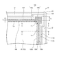
- FIG. 11 is a schematic plan view showing the configuration of the organic EL display panel 90.
- a plurality of organic EL elements are arrayed, and an organic EL element array region 905 having a rectangular outer periphery (two-dot chain line in FIG. 11) is divided into a lower substrate 901, an upper substrate 908, a moisture absorbing wall 909, It is sealed with a sealing wall 910.
- the upper surface of the organic EL element array region 905 corresponds to the display region 91, and the organic EL display panel 90 includes a drive circuit 92 around the display region 91.
- the lower substrate 901 and the upper substrate 908 are flat members that seal the lower and upper portions of the organic EL element array region 905, respectively.
- the sealing wall 910 seals the gap between the lower substrate 901 and the upper substrate 908 and maintains the sealing structure.
- the hygroscopic wall 909 has hygroscopicity, and adsorbs moisture, oxygen, and the like that have entered from the sealing wall 910, thereby suppressing moisture and oxygen from entering the organic EL element array region 905.
- the organic EL display panel 90 includes a sealing layer 906 in addition to the above components.
- the sealing layer 906 prevents contact between the organic EL element array region 905 and the outside air before the sealing structure is formed, and hydrogen and oxygen contained in members in the sealing structure after the sealing structure is formed are arranged in the organic EL element array. In order to prevent contact with the region 905, the upper surface and side surfaces of the organic EL element array region 905 are covered.
- the moisture absorbing wall 909 surrounds the organic EL element array region 905 in a rectangular shape along the outer periphery of the organic EL element array region 905.
- the inventor measured the moisture absorption rate for each of the side part 909a corresponding to the rectangular side formed by the moisture absorption wall 909 and the corner part 909b corresponding to the corner. Specifically, the moisture absorption rate is set to the distance at which moisture permeates from the outer periphery of the moisture absorption wall 909 per hour, and the region of the moisture absorption wall 909 containing calcium oxide powder as a desiccant is observed with an optical microscope. Thus, the penetration distance was measured. In the measurement, the organic EL display panel 90 was performed under accelerated conditions of high temperature and high humidity (60 ° C., 90%).
- FIG. 12 is a graph showing the measurement results of the moisture absorption rate at the side portions 909a and the corner portions 909b of the moisture absorption wall 909.
- the horizontal axis is time (unit: day), and the vertical axis is the moisture penetration distance (unit: ⁇ m) from the outer periphery of the moisture absorbing wall 909.
- the average moisture absorption rate of the corner portion 909b was 15.4 ⁇ m / day, which was nearly twice the average moisture absorption rate of the side portion 909a of 8.5 ⁇ m / day.
- One is that the direction in which moisture and oxygen enter the outside air is one direction at the side portion 909a, but two directions at the corner portion 909b, and the surface area on the outside air per unit volume increases. is there.
- the other is that the corners 909b and the sealing wall 910 have less adhesive strength between the lower substrate 901 side and the upper substrate 908 side than the sides of the side portion 909a and the sealing wall 910, and moisture does not flow. It is because it is easy to invade.
- the moisture absorption capability of the corner portion 909b is saturated first when the moisture absorption capability of the side portion 909a remains.
- the hygroscopic capacity is saturated even in a part of the hygroscopic wall 909, moisture and oxygen in the outside air enter the organic EL element array region 905 from the part, and deteriorate the organic EL element. That is, in the organic EL display panel 90, the organic EL element is deteriorated before the moisture absorbing ability of the moisture absorbing wall 909 is sufficiently exhibited, and the expected life improvement effect cannot be obtained.
- the difference in moisture absorption speed is not limited to the case where the organic EL element array region is enclosed in a rectangular shape like the moisture absorption wall 909, but is considered to occur if the moisture absorption wall has at least one corner on the outer periphery. .
- the present inventor has arrived at one aspect of the present invention described below in order to reduce the deterioration of the organic EL element due to saturation of the partial hygroscopic ability of the hygroscopic wall.
- An organic EL display panel includes a first substrate, a second substrate disposed opposite to the first substrate, and a plurality of organic substrates disposed between the first substrate and the second substrate.
- the organic EL display panel has a hygroscopic property, a moisture absorbing wall that surrounds the outer periphery of the organic EL element arrangement region between the first substrate and the second substrate, and a first substrate that surrounds the outer periphery of the moisture absorbing wall. And a sealing wall that seals a gap with the second substrate.
- the planar shape of the moisture absorbing wall has at least one corner and a side that is a portion other than the corner.
- capacitance when the value which divided each maximum moisture absorption amount in a corner
- the width of the corner is larger than the width of the side.
- the moisture absorption capacity is larger than that of the side part, so even when the moisture absorption rate of the corner part is larger than that of the side part, it is between the side part and the corner part. It is possible to reduce a difference in time when the moisture absorption capacity is saturated. Therefore, the deterioration of the organic EL element due to saturation of the partial hygroscopic ability of the hygroscopic wall is reduced.
- the width of the corner is twice or more than the width of the side. In the organic EL display panel according to the above aspect, it is possible to prevent the moisture absorption capability at the corners of the moisture absorption wall from being saturated before the side portions.
- the corner portions protrude outward from the side portions in the planar shape of the moisture absorption wall according to the above aspect.
- the inner periphery of the moisture absorption wall has a shape along the outer periphery of the organic EL element arrangement region.
- the moisture absorption capacity at the corners can be improved without affecting the formation region of the organic EL element arrangement region, and a framed frame can be realized.
- the outer periphery of the sealing wall has a shape along the outer periphery of the moisture absorption wall.
- angular part is reduced and the difference of the time when the moisture absorption capability between a side part and a corner
- a frame can be formed, and the ratio of the display area to the substrate size can be improved.
- the outer periphery of the organic EL element array region is rectangular, and the outer periphery of the sealing wall is rectangular along the outer periphery of the organic EL element array region.
- Shape In the organic EL display panel according to the above aspect, has a simple shape and can reduce the manufacturing cost.
- the height of the corner portion is larger than the height of the side portion.
- the hygroscopic wall is made of a resin containing a desiccant having hygroscopicity, and the content of the desiccant in the corner portion is in the side portion. It is larger than the content of the desiccant.
- the moisture absorption capacity is larger than that of the side part, so even when the moisture absorption rate of the corner part is larger than that of the side part, it is between the side part and the corner part. It is possible to reduce a difference in time when the moisture absorption capacity is saturated. Therefore, the deterioration of the organic EL element due to saturation of the partial hygroscopic ability of the hygroscopic wall is reduced.
- the method for manufacturing an organic EL display panel includes a first substrate, a second substrate disposed to face the first substrate, and the first substrate and the second substrate.
- An organic EL device comprising: an organic EL device array region in which a plurality of organic EL devices are arrayed; and a sealing wall that surrounds an outer periphery of the organic EL device array region and seals a gap between the first substrate and the second substrate It is a manufacturing method of a display panel. Further, in the manufacturing method, a material having hygroscopicity is disposed on the main surface of the first substrate or the second substrate and inside the region where the sealing wall is disposed, and the planar shape has at least one corner portion.
- a hygroscopic wall surrounding the outer periphery of the organic EL element array region so as to have a side portion other than the corner portion is set larger than the moisture absorption capacity of the side portion.
- an organic EL display panel According to the method for manufacturing an organic EL display panel according to the above aspect, it is possible to manufacture an organic EL display panel that can reduce the deterioration of the organic EL element due to partial saturation of the moisture absorption wall.
- both main surfaces of the organic EL element arrangement region in which a plurality of organic EL elements are arranged are respectively sealed with flat members.
- a material having hygroscopicity is disposed between the flat members, and the planar shape has at least one corner and a side that is a portion other than the corner. In this manner, a moisture absorbing wall surrounding the outer periphery of the organic EL element array region is formed.
- the gap between the flat plate-like members is sealed so as to surround the region where the moisture absorption wall is disposed.
- angular part and the said side part by the length of the inner periphery in each planar shape is made into a moisture absorption capacity
- the moisture absorption capacity of the corner is set larger than the moisture absorption capacity of the side.
- cornerers and “rectangles” do not only indicate exact corners or rectangles, but also include slightly rounded corners, rectangles whose opposing sides are slightly out of parallel, and the like.
- the “planar shape” means a shape appearing in a plan (upper surface) view, specifically, a shape when the target member is projected on a plane parallel to the main surface of the first substrate or the second substrate. Point to.
- the “outer periphery” refers to the outer periphery in the planar shape.
- an organic EL display device 1 including an organic EL display panel 10 which is one embodiment of the present invention will be described with reference to the drawings.
- the drawings of the present application are all schematic, and the scale of the members and the ratio between the vertical direction and the horizontal direction may be different from the actual ones.
- FIG. 1 is a block diagram showing the configuration of the organic EL display device 1.
- the organic EL display device 1 includes an organic EL display panel 10 and a control circuit 20 connected thereto.
- a rectangular display region 11 is disposed at the center, and a drive circuit 12 is disposed around the display region 11.
- a plurality of organic EL elements are arranged in the display area 11, and light is emitted from each organic EL element as a pixel, and an image is displayed in the display area 11.
- the drive circuit 12 includes a power supply circuit that supplies power to each organic EL element, a signal circuit that applies a voltage signal corresponding to a signal from the control circuit 20 to each organic EL element, and an organic that applies a voltage signal at regular intervals. It has a scanning circuit for switching EL elements and drives each organic EL element.
- the control circuit 20 converts data including image information input from the outside into a signal corresponding to the organic EL display panel 10, and outputs the signal to the drive circuit 12, thereby displaying an image to be displayed in the display area 11. Control.
- FIG. 2 is a schematic plan view showing a part of the configuration of the organic EL display panel 10 (hereinafter referred to as “panel 10”).
- 3A is a schematic cross-sectional view taken along the line XX of FIG. 2
- FIG. 3B is a schematic cross-sectional view taken along the line YY of FIG.
- the panel 10 is disposed between the lower substrate 101, the upper substrate 108 disposed opposite to the lower substrate 101, and between the lower substrate 101 and the upper substrate 108.
- the organic EL element array region 105 is a region where a plurality of organic EL elements are arrayed.
- the lower substrate 101 and the upper substrate 108 are one mode of the first substrate and the second substrate in this embodiment.
- substrate in the above are for convenience of explanation, Comprising:
- the upper and lower sides of the panel 10 are not limited.
- the panel 10 surrounds the outer periphery 105a of the organic EL element arrangement region 105 between the lower substrate 101 and the upper substrate 108, and surrounds the outer periphery 109d of the moisture absorption wall 109, and the lower substrate 101 and the upper substrate 108. And a sealing wall 110 for sealing the gap.
- a sealing layer 106 is disposed so as to cover the upper surface and side surfaces of the organic EL element arrangement region 105, and further on the sealing layer 106.
- a resin layer 107 is disposed.
- the panel 10 employs an active matrix method, and includes a TFT layer 102 on the lower substrate 101 in which thin film transistor (TFT) elements that control current supplied to the organic EL elements are arranged.
- the panel 10 also includes a wiring portion 103 that connects the TFT element and an external circuit (drive circuit 12), and an interlayer insulating layer 104 formed on the TFT layer 102.
- the panel 10 employs a top emission method, and the upper substrate 108 side is used as an image display surface.
- the lower substrate 101 is a flat plate-like member that seals the lower side of the organic EL element arrangement region 105 and supports the laminate in the panel 10.
- the TFT layer 102 is a layer in which a pixel drive circuit including a TFT element (not shown) is formed, and is disposed on the main surface of the lower substrate 101.
- the wiring portion 103 is a layer in which a wiring for electrically connecting the TFT element in the TFT layer 102 and an external circuit (drive circuit 12) is formed. As shown in FIG. It is pulled out from the side to the outside of the sealing wall 110.
- the interlayer insulating layer 104 is a layer that prevents unnecessary energization between the TFT layer 102 and the organic EL element array region 105, and is a layer that flattens unevenness on the lower substrate 101 due to the TFT layer 102. It is formed so as to cover the layer 102.
- the interlayer insulating layer 104 has a contact hole (not shown) for electrically connecting the TFT element in the TFT layer 102 and the organic EL element in the organic EL element arrangement region 105 corresponding to the TFT element. Is formed.
- Organic EL element array region 105 The organic EL element arrangement area 105 is a layer in which a plurality of organic EL elements are arranged, and the upper surface thereof corresponds to the display area 11. Therefore, as indicated by a two-dot chain line in FIG. 2, the outer periphery 105a of the organic EL element arrangement region 105 is rectangular. In the panel 10, the organic EL elements are arranged in a two-dimensional direction along the upper surface of the lower substrate 101.
- the organic EL element includes at least a pair of electrodes and an organic light emitting layer containing an organic material sandwiched between the electrodes, and emits light by recombination of holes and electrons supplied from the pair of electrodes in the organic light emitting layer. To do. The amount of light emitted from each organic EL element is determined by the supply current controlled by the corresponding TFT element.
- the organic EL element may have a hole / electron injection layer, a hole / electron transport layer, a hole / electron blocking layer, and the like. Contributes to light emission and long life.
- the organic EL element array region 105 includes partition walls (not shown) for partitioning the organic EL elements, wirings (not shown) connected to the electrodes of the organic EL elements, and the like. Yes.
- the sealing layer 106 has a high sealing property, and moisture and oxygen contained in the sealing structure such as the resin layer 107, the upper substrate 108, and the moisture absorption wall 109 after the sealing structure is formed are organic EL element array regions 105. It is a layer that prevents contact with the surface. Further, the sealing layer 106 may be used as a layer for preventing the organic EL element array region 105 from coming into contact with outside air before forming a sealing structure at the time of manufacture.
- the sealing layer 106 covers not only the upper and outer periphery 105a of the organic EL element array region 105 but also the interlayer insulating layer 104 and the TFT layer 102 which are the underlying layers, and its end surface is the upper surface of the lower substrate 101 (partially It is arranged on the wiring part 103 on the lower substrate 101 (FIGS. 3A and 3B).
- a sealing structure that surrounds all directions of the organic EL element array region 105 is formed by the lower substrate 101 (and the wiring portion 103) having a low moisture and oxygen permeability and the sealing layer 106. can do.
- the sealing layer 106 Since the panel 10 is a top emission type, the sealing layer 106 has translucency so as not to hinder the visibility of the display region 11 and is intermediate to the adjacent layers in the vertical direction. Has a refractive index.
- the resin layer 107 is a layer that flattens the upper surface of the sealing layer 106 and fills a space surrounded by the sealing layer 106, the upper substrate 108, and the moisture absorbing wall 109 to disperse impacts from the outside.
- the resin layer 107 since the panel 10 is a top emission type, the resin layer 107 has translucency so as not to disturb the visibility of the display region 11, and further intermediate refraction with respect to an adjacent layer in the vertical direction. Have a rate.
- the upper substrate 108 is a flat plate-like member that seals above the organic EL element array region 105, and is disposed on the resin layer 107, the moisture absorbing wall 109, and the sealing wall 110.
- the upper substrate 108 has a low transmittance of moisture and oxygen so as to prevent intrusion of moisture and oxygen from the outside air, and has a high light transmittance so as not to disturb the visibility of the display region 11. preferable.
- the upper substrate 108 may be provided with a color filter that adjusts the emission color of the organic EL element.
- the hygroscopic wall 109 has a hygroscopic property that adsorbs moisture, oxygen, and the like, and prevents moisture and oxygen entering from the outside air through the sealing wall 110 from coming into contact with the organic EL element array region 105, for example.
- the moisture absorbing wall 109 has a substantially rectangular planar shape, a side portion 109 a along the outer periphery 105 a of the organic EL element array region 105, and a corner portion that protrudes outward from the side portion 109 a. 109b.
- the inner periphery 109 c of the moisture absorbing wall 109 has a rectangular shape along the outer periphery 105 a of the organic EL element array region 105.
- the corner portion 109b and the side portion 109a are divided by the lengths Lb and La of the inner periphery 109c in the respective planar shapes as the moisture absorption capacity, as described later, the corner portion The moisture absorption capacity of 109b is larger than the moisture absorption capacity of the side 109a.
- the maximum amount of moisture absorption refers to the maximum amount of moisture that can be absorbed by the moisture absorbing wall 109, for example, by a method based on “6.5 Method D” of “JIS K 7209: 2000 Plastic—How to Obtain Water Absorption Rate”. Can be measured.
- the width T2 of the corner portion 109b is more than twice the width T1 of the side portion 109a.
- the side portion 109a is located on the inner side of the end portion of the sealing layer 106 and is disposed on the sealing layer 106. As shown in FIG. Are disposed over the lower substrate 101 from the sealing layer 106 beyond the end of the sealing layer 106. As described above, the panel 10 achieves a frame shape by bringing the moisture absorption wall 109 as close as possible to the organic EL element arrangement region 105.
- the sealing wall 110 is in close contact with the lower substrate 101 and the upper substrate 108 to seal the outer periphery 105a side of the organic EL element arrangement region 105 and as a spacer that maintains the sealing structure of the organic EL element arrangement region 105. Play a role. Therefore, it is preferable to have good adhesion to the lower substrate 101 and the upper substrate 108 and to have a certain rigidity. As shown in FIG. 2, the inner periphery 110c and the outer periphery 110d of the sealing wall 110 have a shape along the outer periphery 109d of the moisture absorbing wall 109, and protrude at positions corresponding to the corner portions 109b.
- the outer periphery 110d side of the sealing wall 110 is outside the end of the sealing layer 106, and the lower substrate 101 and the sealing layer The interface with 106 is sealed. By doing in this way, penetration of moisture and oxygen from the interface can be suppressed.
- Lower substrate 101 For the lower substrate 101, a material having electrical insulation or a semiconductor material such as silicon can be used. Alternatively, a metal material such as stainless steel coated with a material having electrical insulating properties may be used. Examples of the electrically insulating material include alkali-free glass, soda glass, non-fluorescent glass, phosphoric acid glass, boric acid glass, quartz, acrylic resin, styrene resin, polycarbonate resin, epoxy resin, and polyethylene resin. Polyester resin, polyimide resin, silicone resin, aluminum oxide, and the like. In the panel 10, it is preferable to use a material having low permeability such as moisture and oxygen for the lower substrate 101 in order to seal the lower part of the organic EL element arrangement region 105.
- the TFT layer 102 is formed by stacking a semiconductor, a conductor, and an insulator.
- semiconductors include silicon (amorphous, polycrystalline, etc.), oxide semiconductors such as indium-zinc-gallium oxide, and organic materials having a ⁇ -electron conjugated system extending in the planar direction, such as polycyclic aromatic compounds. Can be used.
- the conductor metals such as aluminum, copper, and gold, carbon such as graphite and carbon nanotube, and conductive oxides such as indium tin oxide (ITO) and indium zinc oxide (IZO) can be used.
- silicon nitride, silicon oxide, silicon oxynitride, aluminum oxide, acrylic resin, polyimide resin, siloxane resin, phenol resin, or the like can be used.
- Wiring unit 103 For the wiring portion 103, a conductive material can be used.
- the material exemplified as the conductor of the TFT layer 102 can be used.
- Interlayer insulating layer 104 For the interlayer insulating layer 104, an electrically insulating patternable material, for example, an organic material such as an acrylic resin, a polyimide resin, a siloxane resin, or a phenol resin can be used.
- an organic material such as an acrylic resin, a polyimide resin, a siloxane resin, or a phenol resin.
- Organic EL element array region 105 A conductive material can be used for the electrode and the wiring.
- metals such as aluminum, silver, molybdenum, tungsten, titanium, chromium, nickel, and zinc, alloys such as neodymium-aluminum, gold-aluminum, and magnesium-silver, and conductive oxides such as ITO and IZO can be used. .
- stacked these may be sufficient. Since the panel 10 is a top emission type, the electrode and wiring on the lower substrate 101 side are made of a light reflective material, and the electrode and wiring on the upper substrate 108 side are made of a light transmissive material. It is preferable to use it.
- An organic material that emits light by an electroluminescence phenomenon is used for the organic light emitting layer.
- the partition wall can be made of a material having electrical insulation and capable of forming a fine pattern by processing.
- the organic materials exemplified as the material for the interlayer insulating layer 104 can be used.
- the material of the partition wall has resistance to an organic solvent and does not excessively deform or alter the etching process or baking process.
- the surface of the partition wall is subjected to fluorine treatment or the like, or a material containing fluorine is used for the partition wall so as to have liquid repellency.
- Sealing layer 106 For the sealing layer 106, an inorganic material such as silicon nitride, silicon oxide, silicon oxynitride, or aluminum oxide can be used as a material having low permeability such as moisture and oxygen.
- Resin layer 107 For the resin layer 107, an organic material such as an epoxy resin, an acrylic resin, or a silicone resin can be used.
- Upper substrate 108 As the upper substrate 108, for example, the material exemplified for the lower substrate 101 can be used.
- Hygroscopic wall 109 For the moisture absorbing wall 109, a material having a hygroscopic property, for example, a chemical desiccant containing alkali metal or alkaline earth metal such as quick lime or calcium chloride, or a physical desiccant such as silica gel, aluminum oxide, or zeolite is epoxy-coated. What was contained in resin can be used.
- a material having a hygroscopic property for example, a chemical desiccant containing alkali metal or alkaline earth metal such as quick lime or calcium chloride, or a physical desiccant such as silica gel, aluminum oxide, or zeolite is epoxy-coated. What was contained in resin can be used.
- Sealing wall 110 A material having good adhesion to the lower substrate 101 and the upper substrate 108 can be used for the sealing wall 110. Moreover, since the role as a spacer is given so that the sealing structure of the panel 10 may not be deformed by external pressure, a material having a certain rigidity can be mixed. For example, if the lower substrate 101 and the upper substrate 108 are glass materials or the like, a weldable glass frit can be used. Further, for example, various curable resins such as epoxy resin, urethane resin, and acrylic resin containing particles such as glass and resin can be used.
- Method for Manufacturing Panel 10 An example of the method for manufacturing the panel 10 will be described below. In the following, the method for forming the moisture absorbing wall 109, which is a characteristic configuration of the present application, will be mainly described.
- the lower substrate 101 having the TFT layer 102, the wiring portion 103, and the interlayer insulating layer 104 formed on the upper surface is prepared. Specifically, for example, a thin film is first formed on the lower substrate 101 such as a glass substrate by using a sputtering method, a CVD (Chemical Vapor Deposition) method, a spin coating method, or the like. Then, the TFT layer 102, the wiring portion 103, and the interlayer insulating layer 104 are formed on the lower substrate 101 by patterning the thin film by a photolithography method or the like. At this time, plasma treatment, ion implantation, baking, or the like may be performed as necessary.
- a thin film is first formed on the lower substrate 101 such as a glass substrate by using a sputtering method, a CVD (Chemical Vapor Deposition) method, a spin coating method, or the like.
- the TFT layer 102, the wiring portion 103, and the interlayer insulating layer 104 are
- an organic EL element array region 105 is formed on the lower substrate 101 on which the TFT layer 102, the wiring portion 103, and the interlayer insulating layer 104 are formed.
- a lower electrode is first formed on the lower substrate 101 by sputtering and photolithography. And the material which has photosensitivity is apply
- an upper electrode is formed by a vacuum deposition method, thereby forming an organic EL element. Thereby, the organic EL element arrangement
- the sealing layer 106 is formed so as to cover the organic EL element array region 105 and the outer periphery 105a. Specifically, a silicon nitride layer is formed in a necessary region on the lower substrate 101 on which the organic EL element array region 105 is formed by, for example, a CVD method. As shown in FIGS. 3A and 3B, in the panel 10, the sealing layer 106 is also formed at a position covering the side surfaces of the TFT layer 102 and the interlayer insulating layer 104. It is arranged on 101 and on the wiring part 103. This can be realized, for example, by arranging a mask on the lower substrate 101 in the CVD method and adjusting the opening position of the mask.
- the moisture absorbing material 109 is made of a material for the moisture absorbing wall 109 so as to surround a position corresponding to the organic EL element array region 105 and the sealing layer 106.
- the material 109P is applied by, for example, a dispensing method, a printing method, a die coating method, or the like. At this time, the hygroscopic material 109P is projected outward at the corner 109b forming position than at the side 109a forming position. Details of such a coating method will be described later.
- the sealing material 110P in which the material of the sealing wall 110 is pasted is applied onto the upper substrate 108 around the applied moisture absorbing material 109P by, for example, a dispensing method, a printing method, a die coating method, or the like.
- a resin material 107P such as an epoxy resin is applied on the lower surface side of the upper substrate 108 inside the region where the moisture absorbing material 109P and the sealing material 110P are applied.
- the upper substrate 108 that has also undergone the above steps is disposed, and after applying an appropriate pressure, the sealing material 110P is cured or welded, and the lower substrate 101, the upper substrate 108, A sealing wall 110 for sealing the gap is formed.
- a method of applying the pressure a method of returning both substrates to an atmospheric pressure environment after bonding the lower substrate 101 and the upper substrate 108 formed under vacuum or reduced pressure can be used.
- thermosetting, photocuring, addition of a curing agent, or the like can be used as a method for curing the sealing material 110P.
- a delayed curable material is used for the sealing material 110P so that the laminate on the lower substrate 101 side is not affected, and ultraviolet rays are applied only to the upper substrate 108 before bonding. Irradiation is preferred.
- the sealing material 110P is a glass frit
- the sealing material 110P can be welded to the lower substrate 101 and the upper substrate 108 by a laser.
- the resin material 107P and the moisture absorbent material 109P can be cured and welded to improve the adhesion to the upper substrate 108.
- the resin material 107P and the hygroscopic material 109P become the resin layer 107 and the hygroscopic wall 109, respectively, by the bonding process, regardless of the presence or absence of curing / welding.
- the panel 10 according to the present embodiment can be manufactured.
- region 105 is not restricted to an inkjet method, For example, wet processes, such as a dispensing method, a nozzle coating method, intaglio printing, a relief printing, dry processes, such as a vacuum evaporation method, these dry processes And a wet process.
- a transfer method in which an organic material is transferred from a donor substrate may be used.
- the forming method of each member is not limited to the above method, and a known film forming method and patterning method can be used.
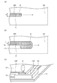
- FIG. 4A is a schematic plan view illustrating a method for forming the side portion 109a
- FIG. 4B is a schematic plan view illustrating a method for forming the corner portion 109b
- FIG. 4C is a method for forming the corner portion 109b. It is a model perspective view explaining these.
- FIG. 4 as an example, a method of applying the moisture absorbing material 109 ⁇ / b> P to the lower surface side of the upper substrate 108 using the dispensing method is described.
- the nozzle N of the dispenser is moved at a constant speed at the position where the side 109a is formed.
- the moisture absorbing material 109P can be applied with the uniform width T3 and the uniform thickness.
- the moving speed of the nozzle is decreased.
- the hygroscopic material 109P can be applied with a width T4 larger than T3. If it does in this way, hygroscopic material 109P can be made to project outside the corner 109b formation position rather than the side 109a formation position.
- the application method using the dispenser is not limited to this, and the application width of the hygroscopic material 109P is not changed between the corner 109b formation position and the side 109a formation position, but the application height of the hygroscopic material 109P is increased. Good. Even in this case, the hygroscopic material 109P spreads in the width direction at the time of bonding, and thus the hygroscopic material 109P can be projected at the corner 109b formation position rather than the side 109a formation position.
- the inside of the application region of the moisture absorbing material 109P may be aligned at the side 109a formation position and the corner 109b formation position. Specifically, as indicated by a line CL through which the center of the nozzle N in FIG. 4B passes, the nozzle N may be shifted outward at the corner 109b formation position.
- the application width T4 of the hygroscopic material 109P at the corner 109b formation position is set to the side 109a formation. What is necessary is just to make it 2 times or more of application
- the application method of the hygroscopic material 109P is not limited to this.
- the method shown in FIG. 4C can be used. Specifically, first, a stack up to the sealing layer 106 is formed on the lower substrate 101. Next, the sealing material 110 ⁇ / b> P is applied with a space from the sealing layer 106. At this time, the gap between the sealing layer 106 and the sealing material 110P is widened at a position corresponding to the corner 109b forming position from a position corresponding to the side 109a forming position. Next, if the hygroscopic material 109P is applied at the above interval, the hygroscopic material 109P can be protruded outward at the corner 109b formation position rather than the side portion 109a formation position.
- the resin material 107P is preferably applied and cured after the sealing material 110P and the hygroscopic material 109P are applied.
- the resin material 107P, the hygroscopic material 109P, and the sealing material 110P are simultaneously cured. Is preferred. If the application and curing of the resin material 107P is performed before the application of the sealing material 110P and the moisture absorbing material 109P, the sealing material 110P and the moisture absorbing material 109P ride on the cured resin layer 107, so that This is because the flatness may be lowered.
- the dispensing method has been described.
- the method of applying the moisture absorbing material 109P is not limited to this, and various wet processes such as a printing method may be used.
- the moisture absorption speed is larger than that of the side portion 109a, but the moisture absorption capacity is also larger than that of the side portion 109a, thereby reducing the difference in time during which the moisture absorption capacity between the side portion 109a and the corner portion 109b is saturated. can do. Therefore, deterioration of the organic EL element due to saturation of the partial moisture absorption capability of the moisture absorption wall 109 is reduced.
- the width T2 of the corner portion 109b is more than twice the width T1 of the side portion. As shown in FIG. 16, the corner portion 109b has a moisture absorption speed that is about twice that of the side portion 109a. Therefore, by setting the width T2 to be twice or more the width T1, the moisture absorption capacity of the corner portion 109b is increased. Can be prevented from being saturated before the side portion 109a.
- the corner 109b projects outward from the side 109a.
- the portion protruding to the outside of the corner portion 109b can be disposed on the lower substrate 101, and from the side portion 109a on the sealing layer 106.
- the height of the moisture absorbing wall 109 (the length in the direction perpendicular to the lower substrate 101) can be increased.
- a laminate such as the TFT layer 102, the interlayer insulating layer 104, and the organic EL element array region 105 often has a forward tapered slope in the height direction at the outer peripheral portion, and the sealing layer 106 that covers these layers is also provided. It is common that it becomes a slope along the same shape. Therefore, when the moisture absorbing wall 109 is disposed close to the sealing layer 106 as in the panel 10, the moisture absorbing wall 109 is positioned on the slope, and the height of the moisture absorbing wall 109 is closer to the outer peripheral side than the inner peripheral side. Since it becomes large, the moisture absorption capacity
- the outer periphery 110 d of the sealing wall 110 has a shape along the outer periphery 109 d of the hygroscopic wall 109. At this time, the sealing wall 110 protrudes outward at a position along the corner portion 109b from a position along the side portion 109a.
- the sealing wall 110 is disposed on the wiring portion 103 and the sealing layer 106 in the portion along the side portion 109 a of the sealing wall 110.
- the sealing wall 110 can be disposed on the lower substrate 101.
- the lower substrate 101 has higher adhesion to the sealing wall 110 and higher flatness than a laminate such as the wiring portion 103 and the sealing layer 106. Therefore, with the above configuration, in the sealing wall 110, moisture and oxygen permeability in a portion along the corner portion 109b can be reduced as compared with a portion along the side portion 109a.
- the protruding portion of the sealing wall 110 has a larger contact area with the base layer than the corners of the rectangular sealing wall 110 having no protrusion, and the adhesion with the base layer is improved.
- the adhesion to the substrate is weaker at the corner than at the side, but with the above structure, the adhesion with the base layer is improved at the corner in the sealing wall 110. It is possible to reduce moisture and oxygen permeability in the corner portion.
- the moisture absorption speed of the corner portion 109b of the moisture absorption wall 109 is reduced, and the difference in time during which the moisture absorption capability between the side portion 109a and the corner portion 109b is saturated can be reduced.
- the portion along the side 109 a of the sealing wall 110 is recessed inward, and the sealing wall 110 A space is formed outside the outer periphery 110d.
- the drive circuit 12 and the like can be arranged in the space.
- the space which corner 109b protrudes, and the space where drive circuit 12 is arranged can be secured without waste. Therefore, the panel 10 can be framed after the drive circuit 12 is arranged, and the ratio of the display area to the substrate size can be improved.
- the panel 10 which concerns on 1 aspect of this invention does not receive a limitation at all by the above embodiment except the essential characteristic component. Below, the modification of the panel 10 is demonstrated as an example of such a form. In addition, about the part similar to the said embodiment, the same code
- FIG. 5 is a schematic plan view showing the configuration of the moisture absorbing wall 209 according to the modification.
- the moisture absorbing wall 209 includes an outer periphery 109d having the same shape as the moisture absorbing wall 109, but the inner periphery 209c is not rectangular but has a shape along the outer periphery 109d.
- the corner portion 209b can be disposed on the lower substrate 101 by the protrusion of the corner portion 209b, and the height of the corner portion 209b can be made larger than the side portion 109a. . Therefore, in the moisture absorption wall 209, the moisture absorption capacity of the corner part 209b can be made larger than the moisture absorption capacity of the side part 109a. That is, even in the panel 10 including the moisture absorption wall 209, the deterioration of the organic EL element array region 105 due to partial saturation of the moisture absorption capacity of the moisture absorption wall 209 is reduced.
- the resin layer 207 can be filled into a space formed by the inner periphery 209c protruding outward at the corner portion 209b. Therefore, if a material having a hygroscopic capacity or a material having low permeability such as moisture or oxygen is used for the resin layer 207, even if the hygroscopic capacity is saturated first in the corner portion 209b, the organic EL element is deteriorated. Can be delayed.
- FIG. 6 is a schematic plan view showing the configuration of the moisture absorbing wall 209W according to the modification.
- the moisture absorbing wall 209W includes a side portion 109a having the same shape as the moisture absorbing wall 109, but the protruding shape of the corner portion 209Wb is not a quadrilateral shape but a pentagonal shape.
- the inner periphery 209Wc of the moisture absorbing wall 209W has a shape along the outer periphery 209Wd.
- the sealing wall 210W is arrange
- the corner portion 209Wb protrudes outward from the side portion 109a, and thus has the same effect as the moisture absorption wall 109.
- the corner portion 209Wb can be disposed on the lower substrate 101 by the protrusion of the corner portion 209Wb, and the height of the corner portion 209Wb can be made larger than the side portion 109a. . Therefore, in the moisture absorption wall 209W, the moisture absorption capacity of the corner portion 209Wb can be made larger than the moisture absorption capacity of the side portion 109a. That is, even in the panel 10 including the moisture absorption wall 209W, the deterioration of the organic EL element arrangement region 105 due to the saturation of the partial moisture absorption capability of the moisture absorption wall 209W is reduced.
- the moisture absorbing wall 209W similarly to the moisture absorbing wall 209, in the moisture absorbing wall 209W, it is also possible to fill the resin layer 207W in a space formed by the inner periphery 209Wc protruding outward at the corner portion 209Wb.
- the protruding shape of the corners of the hygroscopic wall is not limited to the square shape of the hygroscopic walls 109 and 209 and the pentagonal shape of the hygroscopic wall 209W, and may be other polygonal shapes, arc shapes, combinations thereof, or the like. .
- the inner periphery may be a shape along the outer periphery of the organic EL element arrangement region like the moisture absorbing wall 109, or the moisture absorbing walls 209 and 209W
- the shape along the outer periphery of the moisture absorption wall may be sufficient.
- FIG. 7 is a schematic plan view showing the configuration of the sealing wall 210 according to the modification.
- the sealing wall 210 includes an inner periphery 110 c having the same shape as the sealing wall 110, but the outer periphery 210 d has a rectangular shape along the outer periphery 105 a of the organic EL element arrangement region 105. Also in the sealing wall 210, the hygroscopic wall 109 in which the hygroscopic capacity of the corner portion 109b is larger than the hygroscopic capacity of the side portion 109a can be disposed due to the shape of the inner periphery 210c. Therefore, even in the panel 10 including the sealing wall 210, the deterioration of the organic EL element array region 105 due to saturation of the partial moisture absorption capability of the moisture absorption wall 109 is reduced.
- the outer periphery 210d of the sealing wall 210 does not have a protruding portion, and thus the outer periphery of the upper substrate 208 can be rectangular without protruding. Thereby, the manufacture of the upper substrate 208 is simplified, and the manufacturing cost can be reduced.
- FIG. 8 is a schematic plan view showing the configuration of the hygroscopic wall 209X and the sealing wall 210X according to the modification.
- the hygroscopic wall 209 ⁇ / b> X and the sealing wall 210 ⁇ / b> X include the same inner periphery 109 c as the hygroscopic wall 109 and the same outer periphery 210 d as the sealing wall 210, respectively.
- the outer periphery 209Xd of the moisture absorption wall 209X changes so that the width continuously increases from the side portion 109a at the corner portion 209Xb.
- the inner periphery 210Xc of the sealing wall 210X has a shape along the outer periphery 209Xd of the moisture absorption wall 209X.
- the width of the corner portion 209Xb is larger than the width of the side portion 109a, that is, the moisture absorption capacity of the corner portion 209Xb is larger than the moisture absorption capacity of the side portion 109a. Accordingly, even in the panel 10 including the hygroscopic wall 209X and the sealing wall 210X, the deterioration of the organic EL element arrangement region 105 due to partial saturation of the hygroscopic wall 109 is reduced.
- FIG. 9A is a schematic plan view showing the configuration of the moisture absorbing wall 209Y according to the modification
- FIG. 9B is a schematic cross-sectional view taken along the line ZZ in FIG. 9A.
- the moisture absorption wall 209Y includes an inner periphery 109c having the same shape as the moisture absorption wall 109, but the outer periphery 209Yd has a rectangular shape along the inner periphery 109c, similar to the moisture absorption wall 909. ing.
- the lower substrate 201Y has a recessed portion 201Ya that is recessed immediately below the corner portion 209Yb, and the sealing layer 206Y is disposed in the recessed portion 201Ya.
- the moisture absorbing wall 209Y can have a side portion 109a having the same shape as the moisture absorbing wall 109 and a corner portion 209Yb having a height higher than that of the side portion 109a.
- the sealing wall 210Y is disposed along the moisture absorbing wall 209Y, and the inner periphery 210Yc and the outer periphery 210d of the sealing wall 210Y have a shape along the outer periphery 209Yd.
- the moisture absorption capacity of the moisture absorption wall 209Y is proportional not only to the width but also to the amount in the height direction.
- the protruding direction of the corner of the moisture absorption wall is not limited to the lower substrate side, and may protrude to the upper substrate side.
- the main surface may be processed to form a step at the position of the upper substrate corresponding to the corner of the moisture absorption wall, and a large amount of the moisture absorbent 109P may be applied at the corner formation position.
- the panel 10 may include a moisture absorbing wall having a shape in which the corner portion protrudes outside the side portion and also protrudes toward the upper substrate side or the lower substrate side by combining the shapes of the moisture absorbing wall 109 and the moisture absorbing wall 209Y. Good.
- FIG. 10 is a schematic cross-sectional view illustrating a configuration of a moisture absorbing wall 209Z according to a modification.
- the cross section of FIG. 10 has shown the cross section of the same position as the cross section shown to Fig.3 (a).
- the moisture absorbing wall 209Z has an upper portion 209Ze that covers the resin layer 107 in addition to the side portions 109a and the corner portions 109b.
- the moisture absorbing wall 209Z can adsorb moisture, oxygen, and the like contained in the resin layer 107, the upper substrate 108 (when a moisture-permeable member such as a color filter is disposed), and the like. Therefore, in the panel 10 provided with the hygroscopic wall 209Z, it is possible to reduce deterioration of the organic EL element array region 105 due to moisture and oxygen contained in the sealing structure.
- a material (particularly a desiccant) used for the moisture absorbing wall has a low light transmittance, and the light transmittance may change due to moisture absorption. Therefore, when the moisture absorbing wall 209Z is used, it is preferable to use the bottom emission method. .
- the outer periphery 105a of the organic EL element array region 105 has a rectangular shape, but the shape of the organic EL element array region is not limited to this, and has a shape having at least one corner on the outer periphery. If it is.
- it may be a polygonal shape such as a triangle or a pentagon.
- the shape which combined the polygonal shape and the circular arc may be sufficient.
- the end of the sealing layer 106 reaches the lower substrate 101.
- the present invention is not limited to this.
- the end of the sealing layer 106 is formed on the side surface (slope) of the TFT layer 102. It may be arranged.
- the moisture absorbing wall 109 is preferably disposed at a position covering the side surface of the TFT layer 102 exposed from the gap between the lower substrate 101 and the end of the sealing layer 106.
- the panel 10 includes the sealing layer 106, but this is not an essential component and may have a configuration without the sealing layer 106.
- the organic EL element arrangement region 105 and the moisture absorption wall 109 are in direct contact with each other, the organic EL element arrangement region 105 may be deteriorated by moisture or oxygen adsorbed on the inner periphery 109c side of the moisture absorption wall 109. Therefore, it is preferable to arrange a gap between the organic EL element arrangement region 105 and the moisture absorption wall 109.
- the organic EL display device 1 shown in FIG. 1 four drive circuits 12 are provided around the display area.
- the position and number of the drive circuits 12 are not limited to this, for example, only at one end of the display area.
- a drive circuit 12 may be disposed.
- the active matrix method and the top emission method are employed in the panel 10, a passive matrix method and a bottom emission method may be employed.
- the corner portion 109b has a shape protruding outward from the side portion 109a. It is also possible to use other than the above. For example, the shape which the corner
- the inner periphery 109c of the moisture absorbing wall 109 has a shape along the outer periphery 105a of the organic EL element arrangement region 105 as in the panel 10, the ratio of the display region 11 to the substrate size can be further increased, and the frame is narrowed. Can be realized.
- the sealing structure according to one embodiment of the present invention is useful in all electronic circuits using the semiconductivity of organic materials.
- the sealing structure according to one embodiment of the present invention can be applied to organic EL lighting, organic TFT elements, organic photoelectric conversion elements, organic piezoelectric conversion elements, organic transistors, organic integrated circuits, and the like.
- An organic EL display panel, a method for manufacturing an organic EL display panel, and a method for sealing an organic EL element according to the present invention include a device including a display device such as a television device, a commercial display, a personal computer, and a portable electronic device. Can be widely used.
Landscapes
- Electroluminescent Light Sources (AREA)
Abstract
Description
本発明は、内部に有機EL(Electroluminescence)素子が配列された有機EL表示パネルに関し、特に有機EL素子の封止技術に関する。 The present invention relates to an organic EL display panel in which organic EL (Electroluminescence) elements are arranged, and particularly to a sealing technique for organic EL elements.
近年、有機EL素子の発光を画素として利用した有機EL表示パネルについて、研究・開発が行われている。有機EL素子は、少なくとも一対の電極と、当該電極に挟まれた有機発光層とを含み、電極から供給された正孔及び電子の再結合のエネルギーにより発光する。このような有機EL素子を複数配列した有機EL表示パネルは、液晶表示パネルと比較して、応答性、視野角、コントラスト比、軽量化などに優れている。 In recent years, research and development have been conducted on organic EL display panels using light emission of organic EL elements as pixels. The organic EL element includes at least a pair of electrodes and an organic light emitting layer sandwiched between the electrodes, and emits light by energy of recombination of holes and electrons supplied from the electrodes. An organic EL display panel in which a plurality of such organic EL elements are arranged is superior in response, viewing angle, contrast ratio, weight reduction, and the like as compared with a liquid crystal display panel.
ここで有機EL素子には、水分や酸素に対する活性が高い材料が用いられることが多く、そのため有機EL素子は空気中の水分や酸素と反応して劣化しやすい。そこで、有機EL表示パネルにおいては、有機EL素子と外気との接触を抑制する封止技術が重要となる。 Here, a material having high activity with respect to moisture and oxygen is often used for the organic EL element, and therefore, the organic EL element easily reacts with moisture and oxygen in the air and deteriorates easily. Therefore, in an organic EL display panel, a sealing technique that suppresses contact between the organic EL element and the outside air is important.
有機EL表示パネルの封止においては、複数の有機EL素子が配列された有機EL素子配列領域の上方及び下方をガラスなどからなる一対の基板で封止し、硬化性樹脂やガラスフリットなどからなる封止壁で有機EL素子配列領域の外周を囲むとともに基板同士の間隙を封止する構造が一般的である。また、上記構造では外周側からの外気の侵入を十分に抑制できない場合があることから、例えばカルシウムやマグネシウムなどの吸湿性を有する材料を含んだ吸湿壁を有機EL素子配列領域と封止壁との間に配置する構成が開示されている(例えば、特許文献1参照)。有機EL表示パネルでは、挟額縁化や強度確保の要請から、封止壁を可能な限り有機EL素子配列領域に近接させる必要があり、これにより、その中間にある吸湿壁も、可能な限り有機EL素子配列領域に近接して配置される必要がある。例えば、特許文献1では、吸湿壁(乾燥剤9)は、有機EL素子配列領域(発光素子3)の外周に沿って配置されており、その形状は矩形状である。すなわち吸湿壁の平面形状は角部を有する。
In the sealing of the organic EL display panel, the upper and lower sides of the organic EL element arrangement region where a plurality of organic EL elements are arranged are sealed with a pair of substrates made of glass or the like, and are made of a curable resin or glass frit. In general, the sealing wall surrounds the outer periphery of the organic EL element arrangement region and seals the gap between the substrates. In addition, in the above structure, intrusion of outside air from the outer peripheral side may not be sufficiently suppressed, for example, a hygroscopic wall containing a hygroscopic material such as calcium or magnesium is used as the organic EL element arrangement region and the sealing wall. The structure arrange | positioned between these is disclosed (for example, refer patent document 1). In the organic EL display panel, it is necessary to make the sealing wall as close as possible to the organic EL element arrangement region in order to obtain a frame and to ensure the strength. It is necessary to be disposed in the vicinity of the EL element array region. For example, in
本願の発明者は、例えば上記矩形状のような、角部を有する吸湿壁の平面形状において、角部の吸湿速度(単位体積・時間当たりの吸湿量)が他の部分(以下、「辺部」という。)の吸湿速度より大きくなることを発見した。例えば、図11に示すように、有機EL素子配列領域905の外周(図の二点鎖線)に沿って矩形状に有機EL素子配列領域905を囲う吸湿壁909(図の網掛部)を備えた有機EL表示パネル90では、吸湿壁909の辺部909aに比べ、角部909bにおける吸湿速度が大きい。したがって、有機EL表示パネル90では、辺部909aの吸湿能力が残存している段階で、角部909bの吸湿能力が先に飽和する。
The inventor of the present application, for example, in the planar shape of a moisture absorbing wall having a corner, such as the above-described rectangular shape, has a moisture absorption rate (amount of moisture absorbed per unit volume / time) at another corner (hereinafter referred to as “side portion”). "). For example, as shown in FIG. 11, a moisture absorption wall 909 (shaded portion in the figure) surrounding the organic EL element arrangement region 905 in a rectangular shape along the outer periphery (two-dot chain line in the drawing) of the organic EL element arrangement region 905 is provided. In the organic
吸湿壁909の一部分でも吸湿能力が飽和すると、外気中の水分や酸素が当該部分から有機EL素子配列領域905内に侵入し、有機EL素子を劣化させる。つまり、有機EL表示パネル90では、吸湿壁909の吸湿能力が十分に発揮される前に有機EL素子が劣化し、期待するような寿命向上効果が得られない。
When the hygroscopic capacity is saturated even in a part of the hygroscopic wall 909, moisture and oxygen in the outside air enter the organic EL element array region 905 from the part, and deteriorate the organic EL element. That is, in the organic
そこで、本発明の目的は、吸湿壁の部分的な吸湿能力の飽和による有機EL素子の劣化を低減した有機EL表示パネル、そのような有機EL表示パネルの製造方法及び有機EL素子の封止方法を提供することにある。 Accordingly, an object of the present invention is to provide an organic EL display panel in which the deterioration of the organic EL element due to saturation of the partial moisture absorption capacity of the moisture absorbing wall is reduced, a method for manufacturing such an organic EL display panel, and a method for sealing the organic EL element Is to provide.
本発明の一態様に係る有機EL表示パネルは、第1基板と、第1基板と対向して配置された第2基板と、第1基板と第2基板との間に配置され、複数の有機EL素子が配列された有機EL素子配列領域と、を備える。また、当該有機EL表示パネルは、吸湿性を有し、第1基板と第2基板との間において有機EL素子配列領域の外周を囲む吸湿壁と、吸湿壁の外周を囲むとともに第1基板と第2基板との間隙を封止する封止壁と、を備える。さらに、当該有機EL表示パネルでは、吸湿壁の平面形状が、少なくとも一つの角部と、角部以外の部分である辺部と、を有している。そして、当該有機EL表示パネルでは、角部及び辺部における各最大吸湿量を、それぞれの平面形状における内周の長さで割った値を吸湿容量とするとき、角部の吸湿容量が、辺部の吸湿容量よりも大きい。 An organic EL display panel according to one embodiment of the present invention includes a first substrate, a second substrate disposed opposite to the first substrate, and a plurality of organic substrates disposed between the first substrate and the second substrate. An organic EL element arrangement region in which EL elements are arranged. In addition, the organic EL display panel has a hygroscopic property, a moisture absorbing wall that surrounds the outer periphery of the organic EL element arrangement region between the first substrate and the second substrate, and a first substrate that surrounds the outer periphery of the moisture absorbing wall. And a sealing wall that seals a gap with the second substrate. Further, in the organic EL display panel, the planar shape of the moisture absorbing wall has at least one corner and a side that is a portion other than the corner. And in the said organic EL display panel, when the value which divided each maximum moisture absorption amount in a corner | angular part and a side part with the length of the inner periphery in each planar shape is made into a moisture absorption capacity | capacitance, the moisture absorption capacity | capacitance of a corner | angular part is a side. It is larger than the moisture absorption capacity of the part.
上記態様に係る有機EL表示パネルの吸湿壁の角部では、辺部に比べて吸湿容量が大きいため、角部の吸湿速度が辺部よりも大きい場合でも、辺部と角部との間の吸湿能力が飽和する時間の差を低減することができる。したがって、吸湿壁の部分的な吸湿能力の飽和による有機EL素子の劣化が低減する。 In the corner part of the moisture absorption wall of the organic EL display panel according to the above aspect, the moisture absorption capacity is larger than that of the side part, so even when the moisture absorption rate of the corner part is larger than that of the side part, it is between the side part and the corner part. It is possible to reduce a difference in time when the moisture absorption capacity is saturated. Therefore, the deterioration of the organic EL element due to saturation of the partial hygroscopic ability of the hygroscopic wall is reduced.
<本発明の一態様に至った経緯>
本願の発明者(以下、「本発明者」という。)は、角部を有する吸湿壁の平面形状において、角部の吸湿速度が辺部の吸湿速度より大きくなることを発見した。以下にその詳細を示す。
<Background to the Aspect of the Present Invention>
The inventor of the present application (hereinafter referred to as “the present inventor”) has found that the moisture absorption rate at the corners is larger than the moisture absorption rate at the sides in the planar shape of the moisture absorption wall having corners. The details are shown below.
図11は有機EL表示パネル90の構成を示す模式平面図である。有機EL表示パネル90では、複数の有機EL素子が配列され、外周が矩形状(図11の二点鎖線)である有機EL素子配列領域905を、下部基板901、上部基板908、吸湿壁909、封止壁910で封止している。なお、有機EL素子配列領域905の上面は表示領域91に対応しており、有機EL表示パネル90は、表示領域91の周囲に駆動回路92を備えている。
FIG. 11 is a schematic plan view showing the configuration of the organic
下部基板901、上部基板908は、それぞれ有機EL素子配列領域905の下方、上方を封止する平板状の部材である。封止壁910は、下部基板901と上部基板908との間隙を封止し、封止構造を維持している。吸湿壁909は、吸湿性を有し、封止壁910から侵入した水分や酸素などを吸着することで、有機EL素子配列領域905への水分や酸素の侵入を抑制する。なお、有機EL表示パネル90は上記構成要素以外に封止層906を備える。封止層906は、封止構造形成前において有機EL素子配列領域905と外気との接触を防ぐとともに、封止構造形成後に封止構造内の部材に含有された水素や酸素が有機EL素子配列領域905と接触することを防ぐため、有機EL素子配列領域905の上面及び側面を覆っている。
The lower substrate 901 and the upper substrate 908 are flat members that seal the lower and upper portions of the organic EL element array region 905, respectively. The sealing wall 910 seals the gap between the lower substrate 901 and the upper substrate 908 and maintains the sealing structure. The hygroscopic wall 909 has hygroscopicity, and adsorbs moisture, oxygen, and the like that have entered from the sealing wall 910, thereby suppressing moisture and oxygen from entering the organic EL element array region 905. The organic
有機EL表示パネル90では、吸湿壁909は、有機EL素子配列領域905の外周に沿って、矩形状に有機EL素子配列領域905を囲っている。本発明者は、吸湿壁909がなす矩形の辺にあたる辺部909a、角にあたる角部909bのそれぞれについて、吸湿速度の測定を行った。具体的には、吸湿速度を時間当たりに水分が吸湿壁909の外周から侵入した距離とし、乾燥剤として酸化カルシウム粉末を含む吸湿壁909において、吸湿により色が変化した領域を光学顕微鏡で観察することにより、上記侵入距離を測定した。なお、測定においては、有機EL表示パネル90を高温高湿(60℃、90%)の加速条件下において行った。
In the organic
図12は、吸湿壁909の辺部909a及び角部909bにおける吸湿速度の測定結果を示すグラフである。横軸は時間(単位:日)であり、縦軸は吸湿壁909の外周からの水分の侵入距離(単位:μm)である。図に示すとおり、角部909bの平均吸湿速度は15.4μm/dayであり、辺部909aの平均吸湿速度8.5μm/dayの2倍近くとなった。
FIG. 12 is a graph showing the measurement results of the moisture absorption rate at the
本発明者は、この吸湿速度の差異の原因が次の2点であると考えた。一つは、外気中の水分や酸素が侵入する方向が、辺部909aでは一方向であるのに対し、角部909bでは二方向であり、単位体積当たりの外気側の表面積が大きくなるためである。もう一つは、角部909b及び封止壁910の角は、辺部909a及び封止壁910の辺と比較して、下部基板901側及び上部基板908側との密着力が弱く、水分が侵入しやすいためである。
The present inventor considered that the difference in the moisture absorption rate was caused by the following two points. One is that the direction in which moisture and oxygen enter the outside air is one direction at the
このような吸湿速度の差異により、有機EL表示パネル90では、辺部909aの吸湿能力が残存している段階で、角部909bの吸湿能力が先に飽和する。吸湿壁909の一部分でも吸湿能力が飽和すると、外気中の水分や酸素が当該部分から有機EL素子配列領域905内に侵入し、有機EL素子を劣化させる。つまり、有機EL表示パネル90では、吸湿壁909の吸湿能力が十分に発揮される前に有機EL素子が劣化し、期待するような寿命向上効果が得られない。
Due to such a difference in moisture absorption rate, in the organic
なお、上記原因から、吸湿速度の差異は、吸湿壁909のように矩形状に有機EL素子配列領域を囲う場合に限らず、外周に少なくとも一つの角を有する吸湿壁であれば発生すると考えられる。 From the above causes, the difference in moisture absorption speed is not limited to the case where the organic EL element array region is enclosed in a rectangular shape like the moisture absorption wall 909, but is considered to occur if the moisture absorption wall has at least one corner on the outer periphery. .
以上の経緯より、本発明者は、吸湿壁の部分的な吸湿能力の飽和による有機EL素子の劣化を低減させるべく、以下に説明する本発明の一態様に至ったのである。 From the above circumstances, the present inventor has arrived at one aspect of the present invention described below in order to reduce the deterioration of the organic EL element due to saturation of the partial hygroscopic ability of the hygroscopic wall.
<本発明の態様の概要>
本発明の一態様に係る有機EL表示パネルは、第1基板と、第1基板と対向して配置された第2基板と、第1基板と第2基板との間に配置され、複数の有機EL素子が配列された有機EL素子配列領域と、を備える。また、当該有機EL表示パネルは、吸湿性を有し、第1基板と第2基板との間において有機EL素子配列領域の外周を囲む吸湿壁と、吸湿壁の外周を囲むとともに第1基板と第2基板との間隙を封止する封止壁と、を備える。さらに、当該有機EL表示パネルでは、吸湿壁の平面形状が、少なくとも一つの角部と、角部以外の部分である辺部と、を有している。そして、当該有機EL表示パネルでは、角部及び辺部における各最大吸湿量を、それぞれの平面形状における内周の長さで割った値を吸湿容量とするとき、角部の吸湿容量が、辺部の吸湿容量よりも大きい。
<Outline of Aspects of the Present Invention>
An organic EL display panel according to one embodiment of the present invention includes a first substrate, a second substrate disposed opposite to the first substrate, and a plurality of organic substrates disposed between the first substrate and the second substrate. An organic EL element arrangement region in which EL elements are arranged. In addition, the organic EL display panel has a hygroscopic property, a moisture absorbing wall that surrounds the outer periphery of the organic EL element arrangement region between the first substrate and the second substrate, and a first substrate that surrounds the outer periphery of the moisture absorbing wall. And a sealing wall that seals a gap with the second substrate. Further, in the organic EL display panel, the planar shape of the moisture absorbing wall has at least one corner and a side that is a portion other than the corner. And in the said organic EL display panel, when the value which divided each maximum moisture absorption amount in a corner | angular part and a side part with the length of the inner periphery in each planar shape is made into a moisture absorption capacity | capacitance, the moisture absorption capacity | capacitance of a corner | angular part is a side. It is larger than the moisture absorption capacity of the part.
また、本発明の一態様に係る有機EL表示パネルは、上記態様において、吸湿壁の内周と外周との間隔を幅とするとき、角部の幅が、辺部の幅よりも大きい。 Further, in the organic EL display panel according to one aspect of the present invention, in the above aspect, when the interval between the inner periphery and the outer periphery of the moisture absorption wall is a width, the width of the corner is larger than the width of the side.
上記態様に係る有機EL表示パネルの吸湿壁の角部では、辺部に比べて吸湿容量が大きいため、角部の吸湿速度が辺部よりも大きい場合でも、辺部と角部との間の吸湿能力が飽和する時間の差を低減することができる。したがって、吸湿壁の部分的な吸湿能力の飽和による有機EL素子の劣化が低減する。 In the corner part of the moisture absorption wall of the organic EL display panel according to the above aspect, the moisture absorption capacity is larger than that of the side part, so even when the moisture absorption rate of the corner part is larger than that of the side part, it is between the side part and the corner part. It is possible to reduce a difference in time when the moisture absorption capacity is saturated. Therefore, the deterioration of the organic EL element due to saturation of the partial hygroscopic ability of the hygroscopic wall is reduced.
また、本発明の一態様に係る有機EL表示パネルは、上記態様において、角部の幅が、辺部の幅の2倍以上である。上記態様に係る有機EL表示パネルでは、吸湿壁の角部の吸湿能力が辺部よりも先に飽和することを防ぐことができる。 Further, in the organic EL display panel according to one aspect of the present invention, in the above aspect, the width of the corner is twice or more than the width of the side. In the organic EL display panel according to the above aspect, it is possible to prevent the moisture absorption capability at the corners of the moisture absorption wall from being saturated before the side portions.
また、本発明の一態様に係る有機EL表示パネルは、上記態様の吸湿壁の平面形状において、角部が、辺部より外側に突出する。 Further, in the organic EL display panel according to one aspect of the present invention, the corner portions protrude outward from the side portions in the planar shape of the moisture absorption wall according to the above aspect.
また、本発明の一態様に係る有機EL表示パネルは、上記態様において、吸湿壁の内周が有機EL素子配列領域の外周に沿った形状である。 Further, in the organic EL display panel according to one aspect of the present invention, in the above aspect, the inner periphery of the moisture absorption wall has a shape along the outer periphery of the organic EL element arrangement region.
上記態様に係る有機EL表示パネルでは、有機EL素子配列領域の形成領域に影響を与えることなく角部の吸湿容量を向上でき、挟額縁化が実現できる。 In the organic EL display panel according to the above aspect, the moisture absorption capacity at the corners can be improved without affecting the formation region of the organic EL element arrangement region, and a framed frame can be realized.
また、本発明の一態様に係る有機EL表示パネルは、上記態様において、封止壁の外周が、吸湿壁の外周に沿った形状である。上記態様に係る有機EL表示パネルでは、角部に沿った封止壁の部分における水分や酸素の透過性を低減することができる。これにより、当該有機EL表示パネルでは、角部の吸湿速度が低減され、辺部と角部との間の吸湿能力が飽和する時間の差を低減することができる。また、駆動回路を配置する場合であっても、挟額縁化を実現でき、基板サイズに占める表示領域の割合を向上させることができる。 Further, in the organic EL display panel according to one aspect of the present invention, in the above aspect, the outer periphery of the sealing wall has a shape along the outer periphery of the moisture absorption wall. In the organic EL display panel according to the above aspect, it is possible to reduce moisture and oxygen permeability in the portion of the sealing wall along the corner. Thereby, in the said organic EL display panel, the moisture absorption speed | rate of a corner | angular part is reduced and the difference of the time when the moisture absorption capability between a side part and a corner | angular part is saturated can be reduced. Further, even when the drive circuit is arranged, a frame can be formed, and the ratio of the display area to the substrate size can be improved.
また、本発明の一態様に係る有機EL表示パネルは、上記態様において、有機EL素子配列領域の外周が矩形状であり、封止壁の外周が、有機EL素子配列領域の外周に沿った矩形状である。上記態様に係る有機EL表示パネルは、簡易な形状であり、製造コストを低減できる。 In the organic EL display panel according to one aspect of the present invention, in the above aspect, the outer periphery of the organic EL element array region is rectangular, and the outer periphery of the sealing wall is rectangular along the outer periphery of the organic EL element array region. Shape. The organic EL display panel according to the above aspect has a simple shape and can reduce the manufacturing cost.
また、本発明の一態様に係る有機EL表示パネルは、上記態様において、前記角部の高さが、前記辺部の高さよりも大きい。 Further, in the organic EL display panel according to an aspect of the present invention, in the above aspect, the height of the corner portion is larger than the height of the side portion.
また、本発明の一態様に係る有機EL表示パネルは、上記態様において、吸湿壁が、吸湿性を有する乾燥剤を含有させた樹脂からなり、角部における乾燥剤の含有率が、辺部における乾燥剤の含有率よりも大きい。 Further, in the organic EL display panel according to one embodiment of the present invention, in the above embodiment, the hygroscopic wall is made of a resin containing a desiccant having hygroscopicity, and the content of the desiccant in the corner portion is in the side portion. It is larger than the content of the desiccant.
上記態様に係る有機EL表示パネルの吸湿壁の角部では、辺部に比べて吸湿容量が大きいため、角部の吸湿速度が辺部よりも大きい場合でも、辺部と角部との間の吸湿能力が飽和する時間の差を低減することができる。したがって、吸湿壁の部分的な吸湿能力の飽和による有機EL素子の劣化が低減する。 In the corner part of the moisture absorption wall of the organic EL display panel according to the above aspect, the moisture absorption capacity is larger than that of the side part, so even when the moisture absorption rate of the corner part is larger than that of the side part, it is between the side part and the corner part. It is possible to reduce a difference in time when the moisture absorption capacity is saturated. Therefore, the deterioration of the organic EL element due to saturation of the partial hygroscopic ability of the hygroscopic wall is reduced.
また、本発明の一態様に係る有機EL表示パネルの製造方法は、第1基板と、第1基板と対向して配置された第2基板と、第1基板と第2基板との間に配置され複数の有機EL素子が配列された有機EL素子配列領域と、有機EL素子配列領域の外周を囲むとともに第1基板と第2基板との間隙を封止する封止壁とを備えた有機EL表示パネルの製造方法である。また、当該製造方法では、第1基板又は第2基板の主面上であって封止壁が配置される領域の内側に吸湿性を有する材料を配置して、平面形状が少なくとも一つの角部と、角部以外の部分である辺部とを有するように有機EL素子配列領域の外周を囲む吸湿壁を形成する。さらに、当該製造方法では、吸湿壁を形成する際に、角部及び辺部における各最大吸湿量を、それぞれの平面形状における内周の長さで割った値を吸湿容量とするとき、角部の吸湿容量を、辺部の吸湿容量よりも大きく設定する。 The method for manufacturing an organic EL display panel according to one aspect of the present invention includes a first substrate, a second substrate disposed to face the first substrate, and the first substrate and the second substrate. An organic EL device comprising: an organic EL device array region in which a plurality of organic EL devices are arrayed; and a sealing wall that surrounds an outer periphery of the organic EL device array region and seals a gap between the first substrate and the second substrate It is a manufacturing method of a display panel. Further, in the manufacturing method, a material having hygroscopicity is disposed on the main surface of the first substrate or the second substrate and inside the region where the sealing wall is disposed, and the planar shape has at least one corner portion. And a hygroscopic wall surrounding the outer periphery of the organic EL element array region so as to have a side portion other than the corner portion. Further, in the manufacturing method, when forming the moisture absorption wall, when the maximum moisture absorption amount at the corner and the side is divided by the length of the inner circumference in each planar shape, Is set larger than the moisture absorption capacity of the side portion.
上記態様に係る有機EL表示パネルの製造方法によれば、吸湿壁の部分的な吸湿能力の飽和による有機EL素子の劣化の発生を低減できる有機EL表示パネルが製造できる。 According to the method for manufacturing an organic EL display panel according to the above aspect, it is possible to manufacture an organic EL display panel that can reduce the deterioration of the organic EL element due to partial saturation of the moisture absorption wall.
また、本発明の一態様に係る有機EL素子の封止方法は、複数の有機EL素子が配列された有機EL素子配列領域の両主面をそれぞれ平板状の部材によって封止する。さらに、当該封止方法では、平板状の部材同士の間に、吸湿性を有する材料を配置して、平面形状が少なくとも一つの角部と、前記角部以外の部分である辺部とを有するように前記有機EL素子配列領域の外周を囲む吸湿壁を形成する。さらに、当該封止方法では、吸湿壁が配置される領域を囲むように、平板状の部材同士の間隙を封止する。そして、当該封止方法では、前記吸湿壁を形成する際に、前記角部及び前記辺部における各最大吸湿量を、それぞれの平面形状における内周の長さで割った値を吸湿容量とするとき、前記角部の吸湿容量を、前記辺部の吸湿容量よりも大きく設定する。 Further, in the organic EL element sealing method according to one embodiment of the present invention, both main surfaces of the organic EL element arrangement region in which a plurality of organic EL elements are arranged are respectively sealed with flat members. Further, in the sealing method, a material having hygroscopicity is disposed between the flat members, and the planar shape has at least one corner and a side that is a portion other than the corner. In this manner, a moisture absorbing wall surrounding the outer periphery of the organic EL element array region is formed. Furthermore, in the sealing method, the gap between the flat plate-like members is sealed so as to surround the region where the moisture absorption wall is disposed. And in the said sealing method, when forming the said moisture absorption wall, the value which divided each maximum moisture absorption amount in the said corner | angular part and the said side part by the length of the inner periphery in each planar shape is made into a moisture absorption capacity | capacitance. The moisture absorption capacity of the corner is set larger than the moisture absorption capacity of the side.
上記態様に係る有機EL素子の封止方法によれば、吸湿壁の部分的な吸湿能力の飽和による有機EL素子の劣化を低減することができる。 According to the method for sealing an organic EL element according to the above aspect, it is possible to reduce deterioration of the organic EL element due to saturation of the partial moisture absorption capability of the moisture absorption wall.
なお、本願において「角」、「矩形」とは厳密な角、矩形のみを指すものではなく、多少の丸みを帯びている角や、対向する辺が平行から多少ずれている矩形なども含むものである。また、「平面形状」とは、平面(上面)図にて現れる形状を意味し、具体的には、第1基板又は第2基板の主面と平行な面に対象部材を投影した際の形状を指す。 さらに、「外周」とは、上記平面形状における外周を指す。 In the present application, “corners” and “rectangles” do not only indicate exact corners or rectangles, but also include slightly rounded corners, rectangles whose opposing sides are slightly out of parallel, and the like. . Further, the “planar shape” means a shape appearing in a plan (upper surface) view, specifically, a shape when the target member is projected on a plane parallel to the main surface of the first substrate or the second substrate. Point to. Furthermore, the “outer periphery” refers to the outer periphery in the planar shape.
<実施の形態>
以下では、実施の形態として、本発明の一態様である有機EL表示パネル10を備えた有機EL表示装置1について、図面を用いて説明する。なお、本願の図面はすべて模式的なものであり、部材の縮尺や、縦方向と横方向との比率は、実際のものとは異なる場合がある。
<Embodiment>
Hereinafter, as an embodiment, an organic
1.有機EL表示装置1の構成
図1は有機EL表示装置1の構成を示すブロック図である。有機EL表示装置1は、有機EL表示パネル10と、これに接続された制御回路20とを備える。有機EL表示パネル10には、その中央に矩形状の表示領域11が配置され、表示領域11の周囲に駆動回路12が配置されている。
1. Configuration of Organic
表示領域11には、複数の有機EL素子(不図示)が配列されており、各有機EL素子の発光が画素となって表示領域11に画像が表示される。駆動回路12は、各有機EL素子に電力を供給する電源回路、制御回路20からの信号に応じた電圧信号を有機EL素子ごとに印加する信号回路、一定の間隔ごとに電圧信号を印加する有機EL素子を切り替える走査回路などを有し、各有機EL素子を駆動する。制御回路20は、外部から入力された画像情報を含むデータを、有機EL表示パネル10に対応した信号に変換し、当該信号を駆動回路12に出力することで、表示領域11に表示する画像を制御する。
A plurality of organic EL elements (not shown) are arranged in the
2.有機EL表示パネル10の構成
(1)全体構成
有機EL表示パネル10の全体構成について、図2及び図3を用いて説明する。図2は、有機EL表示パネル10(以下、「パネル10」という。)の構成の一部を示す模式平面図である。また、図3(a)は、図2のX-X線における模式断面図であり、図3(b)は、図2のY-Y線における模式断面図である。
2. Configuration of Organic EL Display Panel 10 (1) Overall Configuration The overall configuration of the organic
図2及び図3に示すように、パネル10は、下部基板101と、下部基板101と対向して配置された上部基板108と、下部基板101と上部基板108との間に配置され、平面形状における外周105aが矩形状となった有機EL素子配列領域105とを備える。なお、有機EL素子配列領域105は、複数の有機EL素子が配列された領域である。ここで、下部基板101、上部基板108は、本実施の形態における第1基板、第2基板の一態様である。なお、上記における基板の上下は説明の便宜上のものであって、パネル10の上下を限定するものではない。
As shown in FIGS. 2 and 3, the
また、パネル10は、下部基板101と上部基板108との間において有機EL素子配列領域105の外周105aを囲む吸湿壁109と、吸湿壁109の外周109dを囲むとともに下部基板101と上部基板108との間隙を封止する封止壁110とを備える。なお、図3(a)、(b)に示すように、パネル10では、有機EL素子配列領域105の上面及び側面を覆うように封止層106が配置され、さらに封止層106上には樹脂層107が配置されている。
Further, the
なお、パネル10は、アクティブマトリクス方式を採用し、有機EL素子に供給する電流を制御する薄膜トランジスタ(TFT)素子が内部に配列されたTFT層102を下部基板101上に備える。また、パネル10は、当該TFT素子と外部回路(駆動回路12)とを接続する配線部103と、TFT層102上に形成された層間絶縁層104とを備える。また、パネル10は、トップエミッション方式を採用し、上部基板108側を画像表示面としている。
The
(2)各部の説明
a.下部基板101
下部基板101は、有機EL素子配列領域105の下方を封止し、かつパネル10において積層物を支持する平板状の部材である。
(2) Explanation of each part a.
The
b.TFT層102
TFT層102は、TFT素子(不図示)を含む画素の駆動回路が内部に形成された層であり、下部基板101の主面上に配置されている。
b.
The
c.配線部103
配線部103は、TFT層102内のTFT素子と外部回路(駆動回路12)とを電気的に接続する配線が形成された層であり、図3(a)に示すように、TFT層の側面側から封止壁110の外側に引き出されている。
c.
The
d.層間絶縁層104
層間絶縁層104は、TFT層102と有機EL素子配列領域105との不要な通電を防止する層であり、かつ、TFT層102による下部基板101上の凹凸を平坦化する層であって、TFT層102上を覆うように形成されている。また、層間絶縁層104には、TFT層102内のTFT素子と、当該TFT素子に対応する有機EL素子配列領域105内の有機EL素子とを電気的に接続するため、コンタクトホール(不図示)が形成されている。
d.
The interlayer insulating
e.有機EL素子配列領域105
有機EL素子配列領域105は、複数の有機EL素子が配列された層であり、その上面は表示領域11に対応する。したがって、図2の二点鎖線で示すように、有機EL素子配列領域105の外周105aは矩形状である。なお、パネル10では、有機EL素子は、下部基板101上面に沿った二次元方向に配列される。
e. Organic EL
The organic EL
有機EL素子は、少なくとも一対の電極と、当該電極に挟まれた有機材料を含む有機発光層とからなり、一対の電極から供給された正孔及び電子が有機発光層で再結合することにより発光する。各有機EL素子の発光の量は、対応するTFT素子に制御された供給電流によって決まる。なお、有機EL素子は、正孔・電子注入層、正孔・電子輸送層、正孔・電子阻止層などを有していてもよく、これらの層は有機EL素子の低電圧駆動、高効率発光、高寿命などに寄与する。 The organic EL element includes at least a pair of electrodes and an organic light emitting layer containing an organic material sandwiched between the electrodes, and emits light by recombination of holes and electrons supplied from the pair of electrodes in the organic light emitting layer. To do. The amount of light emitted from each organic EL element is determined by the supply current controlled by the corresponding TFT element. The organic EL element may have a hole / electron injection layer, a hole / electron transport layer, a hole / electron blocking layer, and the like. Contributes to light emission and long life.
また、有機EL素子配列領域105には、有機EL素子以外にも、有機EL素子間を区画する隔壁(不図示)や有機EL素子の電極に接続された配線(不図示)などが配置されている。
In addition to the organic EL elements, the organic EL
f.封止層106
封止層106は、高い封止性を有し、封止構造形成後に樹脂層107、上部基板108、吸湿壁109などの封止構造内に含有された水分や酸素が有機EL素子配列領域105と接触することなどを防ぐ層である。また、封止層106は、製造時の封止構造形成前に有機EL素子配列領域105が外気と接触することを防ぐ層として用いられる場合もある。
f.
The
封止層106は、有機EL素子配列領域105の上方及び外周105aだけでなく、その下地層である層間絶縁層104及びTFT層102も覆っており、その端面は下部基板101上面(一部は下部基板101上の配線部103上)に配置されている(図3(a)、(b))。上記のような構造を取ることで、水分や酸素の透過性の低い下部基板101(及び配線部103)と封止層106とで有機EL素子配列領域105の全方位を囲う封止構造を形成することができる。なお、パネル10はトップエミッション型であるため、封止層106は、表示領域11の視認性を妨げないよう、透光性を有しており、さらに上下方向の隣接層に対して中間的な屈折率を有する。
The
g.樹脂層107
樹脂層107は、封止層106の上面を平坦化し、かつ封止層106、上部基板108及び吸湿壁109に囲まれる空間を埋めて外部からの衝撃を分散させる層である。なお、パネル10はトップエミッション型であるため、樹脂層107は、表示領域11の視認性を妨げないよう、透光性を有しており、さらに上下方向の隣接層に対して中間的な屈折率を有する。
g.
The
h.上部基板108
上部基板108は、有機EL素子配列領域105の上方を封止する平板状の部材であり、樹脂層107、吸湿壁109及び封止壁110上に配置される。上部基板108は、外気の水分や酸素などの侵入を防ぐことができるように水分や酸素などの透過性が低く、また、表示領域11の視認性を妨げないよう、光透過率が高いことが好ましい。また、上部基板108には、有機EL素子の発光色を調整するカラーフィルタを配置してもよい。
h.
The
i.吸湿壁109
吸湿壁109は、水分や酸素などを吸着する吸湿性を有し、例えば外気から封止壁110を介して侵入する水分や酸素が有機EL素子配列領域105と接触することを防ぐものである。吸湿壁109は、図2に示すように、その平面形状が、略矩形状であり、有機EL素子配列領域105の外周105aに沿った辺部109aと、辺部109aより外側に突出する角部109bを有している。また、吸湿壁109の内周109cは、有機EL素子配列領域105の外周105aに沿った矩形状となっている。
i.
The
パネル10では、角部109b及び辺部109aにおける各最大吸湿量を、それぞれの平面形状における内周109cの長さLb、Laで割った値を吸湿容量とするとき、後述するように、角部109bの吸湿容量が、辺部109aの吸湿容量よりも大きい。ここで、最大吸湿量とは、吸湿壁109が吸湿できる最大水分量を指し、例えば、「JIS K 7209:2000 プラスチック-吸水率の求め方」の「6.5 D法」に準拠した方法により測定することができる。
In the
さらにパネル10では、吸湿壁109の内周109cと外周109dとの間隔を幅とするとき、角部109bの幅T2は、辺部109aの幅T1の2倍以上となっている。
Furthermore, in the
図3(a)に示すように、辺部109aは封止層106の端部よりも内側に位置し、封止層106上に配置され、図3(b)に示すように、角部109bは、封止層106上から封止層106の端部を超えて下部基板101上に渡って配置されている。このように、吸湿壁109を有機EL素子配列領域105に可能な限り近接させることで、パネル10では、挟額縁化を実現している。
As shown in FIG. 3A, the
j.封止壁110
封止壁110は、下部基板101と上部基板108と密着して、有機EL素子配列領域105の外周105a側を封止するとともに、有機EL素子配列領域105の封止構造を維持するスペーサとしての役割を果たす。したがって、下部基板101及び上部基板108と良好な密着性を有し、一定の剛性を有することが好ましい。図2に示すように封止壁110の内周110c及び外周110dは、吸湿壁109の外周109dに沿った形状を有し、角部109bに対応する位置で突出している。
j. Sealing
The sealing
なお、図3(a)、(b)に示すように、パネル10では、封止壁110の外周110d側は、封止層106の端部よりも外側にあり、下部基板101と封止層106との界面を封止している。このようにすることで、当該界面からの水分や酸素の浸透を抑制できる。
3A and 3B, in the
(3)各部の材料
パネル10を構成する各部の材料について、以下に説明する。なお、以下に記載した材料は例示であって、同様の機能を有する材料を用いてもよい。
(3) Material of each part The material of each part which comprises the
a.下部基板101
下部基板101には、電気絶縁性を有する材料又はシリコンなどの半導体材料を用いることができる。また、電気絶縁性を有する材料をコーティングしたステンレスなどの金属材料などを用いてもよい。電気絶縁性を有する材料は、例えば、無アルカリガラス、ソーダガラス、無蛍光ガラス、燐酸系ガラス、硼酸系ガラス、石英、アクリル系樹脂、スチレン系樹脂、ポリカーボネート系樹脂、エポキシ系樹脂、ポリエチレン系樹脂、ポリエステル系樹脂、ポリイミド系樹脂、シリコーン系樹脂、酸化アルミニウムなどである。なお、パネル10において、下部基板101には、有機EL素子配列領域105の下方を封止するために、水分や酸素などの透過性が低い材料を用いることが好ましい。
a.
For the
b.TFT層102
TFT層102は、半導体、導電体、絶縁体の積層により構成される。半導体としては、例えば、シリコン(非晶質、多結晶など)、インジウム-亜鉛-ガリウム酸化物などの酸化物半導体、多環芳香族化合物など平面方向に広がったπ電子共役系を有する有機材料などを用いることができる。導電体としては、アルミニウム、銅、金などの金属、黒鉛、カーボンナノチューブなどの炭素、酸化インジウムスズ(ITO)や酸化インジウム亜鉛(IZO)などの導電性酸化物などを用いることができる。また、絶縁体としては、窒化シリコン、酸化シリコン、酸窒化シリコン、酸化アルミニウム、アクリル系樹脂、ポリイミド系樹脂、シロキサン系樹脂、フェノール系樹脂などを用いることができる。
b.
The
c.配線部103
配線部103には、導電性を有する材料を用いることができ、例えば、上記TFT層102の導電体として例示した材料を用いることができる。
c.
For the
d.層間絶縁層104
層間絶縁層104には、電気絶縁性を有するパターニング可能な材料、例えば、アクリル系樹脂、ポリイミド系樹脂、シロキサン系樹脂、フェノール系樹脂などの有機材料を用いることができる。
d.
For the
e.有機EL素子配列領域105
電極及び配線には、導電性を有する材料を用いることができる。例えば、アルミニウム、銀、モリブデン、タングステン、チタン、クロム、ニッケル、亜鉛などの金属、ネオジウム-アルミニウム、金-アルミニウム、マグネシウム-銀などの合金、ITOやIZOなどの導電性酸化物を用いることができる。また、これらを積層した多層構造などであってもよい。なお、パネル10は、トップエミッション型であるため、下部基板101側の電極及び配線には、光反射性を有する材料を、上部基板108側の電極及び配線には、光透過性を有する材料を用いることが好ましい。
e. Organic EL
A conductive material can be used for the electrode and the wiring. For example, metals such as aluminum, silver, molybdenum, tungsten, titanium, chromium, nickel, and zinc, alloys such as neodymium-aluminum, gold-aluminum, and magnesium-silver, and conductive oxides such as ITO and IZO can be used. . Moreover, the multilayer structure etc. which laminated | stacked these may be sufficient. Since the
有機発光層には、電界発光現象によって発光する有機材料を用いる。具体的には、例えば、オキシノイド化合物、ペリレン化合物、クマリン化合物、アザクマリン化合物、オキサゾール化合物、オキサジアゾール化合物、ペリノン化合物、ピロロピロール化合物、ナフタレン化合物、アントラセン化合物、フルオレン化合物、フルオランテン化合物、テトラセン化合物、ピレン化合物、コロネン化合物、キノロン化合物、アザキノロン化合物、ピラゾリン誘導体、ピラゾロン誘導体、ローダミン化合物、クリセン化合物、フェナントレン化合物、シクロペンタジエン化合物、スチルベン化合物、ジフェニルキノン化合物、スチリル化合物、ブタジエン化合物、ジシアノメチレンピラン化合物、ジシアノメチレンチオピラン化合物、フルオレセイン化合物、ピリリウム化合物、チアピリリウム化合物、セレナピリリウム化合物、テルロピリリウム化合物、芳香族アルダジエン化合物、オリゴフェニレン化合物、チオキサンテン化合物、シアニン化合物、アクリジン化合物、8-ヒドロキシキノリン化合物の金属錯体、2-ビピリジン化合物の金属錯体、シッフ塩とIII族金属との錯体、オキシン金属錯体、希土類錯体等の蛍光物質(いずれも特開平5-163488号公報に記載)などの公知の蛍光物質、燐光物質を用いることができる。また、例えば、上記の蛍光物質、燐光物質をドーパントとした有機化合物の混合層を用いてもよい。 An organic material that emits light by an electroluminescence phenomenon is used for the organic light emitting layer. Specifically, for example, oxinoid compounds, perylene compounds, coumarin compounds, azacoumarin compounds, oxazole compounds, oxadiazole compounds, perinone compounds, pyrrolopyrrole compounds, naphthalene compounds, anthracene compounds, fluorene compounds, fluoranthene compounds, tetracene compounds, pyrenes Compound, coronene compound, quinolone compound, azaquinolone compound, pyrazoline derivative, pyrazolone derivative, rhodamine compound, chrysene compound, phenanthrene compound, cyclopentadiene compound, stilbene compound, diphenylquinone compound, styryl compound, butadiene compound, dicyanomethylenepyran compound, dicyanomethylene Thiopyran compounds, fluorescein compounds, pyrylium compounds, thiapyrylium compounds, serenapyrine Compounds, telluropylium compounds, aromatic ardadiene compounds, oligophenylene compounds, thioxanthene compounds, cyanine compounds, acridine compounds, metal complexes of 8-hydroxyquinoline compounds, metal complexes of 2-bipyridine compounds, Schiff salts and group III metals Known fluorescent materials and phosphorescent materials such as fluorescent materials such as complexes, oxine metal complexes, and rare earth complexes (all described in JP-A-5-163488) can be used. Further, for example, a mixed layer of an organic compound using the above-described fluorescent substance or phosphorescent substance as a dopant may be used.
隔壁には、電気絶縁性を有し、加工により微細なパターンが形成可能な材料を用いることができる。例えば、層間絶縁層104の材料として例示した有機材料を用いることができる。なお、隔壁の材料は、有機溶剤への耐性を有し、エッチング処理やベーク処理に対して過度に変形、変質などをしないものが好ましい。また、有機発光層の形成に湿式プロセスを用いる場合は、隔壁の表面にフッ素処理などを行うか、隔壁にフッ素を含んだ材料を用い、撥液性を持たせることが好ましい。
The partition wall can be made of a material having electrical insulation and capable of forming a fine pattern by processing. For example, the organic materials exemplified as the material for the interlayer insulating
f.封止層106
封止層106には、水分や酸素などの透過性が低い材料として、窒化シリコン、酸化シリコン、酸窒化シリコン、酸化アルミニウムなどの無機材料を用いることができる。
f.
For the
g.樹脂層107
樹脂層107には、エポキシ樹脂、アクリル樹脂、シリコーン樹脂などの有機材料を用いることができる。
g.
For the
h.上部基板108
上部基板108には、例えば、下部基板101の材料として例示したものを用いることができる。
h.
As the
i.吸湿壁109
吸湿壁109には、吸湿性を有する材料、例えば、生石灰、塩化カルシウムなど、アルカリ金属やアルカリ土類金属を含んだ化学的乾燥剤や、シリカゲル、酸化アルミニウム、ゼオライトなどの物理的乾燥剤をエポキシ樹脂に含有させたものなどを用いることができる。
i.
For the
j.封止壁110
封止壁110には、下部基板101及び上部基板108と良好な密着性を有する材料を用いることができる。また、外圧によりパネル10の封止構造が変形しないようにスペーサとしての役割を持たせるため、一定の剛性を有する材料を混合させることができる。例えば、下部基板101及び上部基板108がガラス材料などであれば、溶着可能なガラスフリットを用いることができる。また、例えば、エポキシ樹脂、ウレタン樹脂、アクリル樹脂などの各種硬化性樹脂にガラスや樹脂などの粒子を含有させたものを用いることができる。
j. Sealing
A material having good adhesion to the
3.パネル10の製造方法
パネル10の製造方法について、以下に一例を説明する。なお、以下では、本願の特徴的な構成である吸湿壁109の形成方法を中心に説明する。
3. Method for
(1)製造方法の概略
a.下部基板準備工程
まず上面にTFT層102、配線部103及び層間絶縁層104が形成された下部基板101を準備する。具体的には、例えば、まずガラス基板などの下部基板101上にスパッタ法、CVD(Chemical Vapor Deposition)法、スピンコート法などを用いて薄膜を形成する。そして、フォトリソグラフィー法などによって薄膜をパターニングすることで、下部基板101上にTFT層102、配線部103及び層間絶縁層104を形成する。この際、必要に応じて、プラズマ処理、イオン注入、ベーキングなどの処理を行ってもよい。
(1) Outline of production method a. Lower substrate preparation step First, the
b.有機EL素子配列領域形成工程
次に、TFT層102、配線部103及び層間絶縁層104が形成された下部基板101上に有機EL素子配列領域105を形成する。具体的には、例えば、まず下部基板101上に、スパッタリング及びフォトリソグラフィーにより下部側の電極を形成する。そして、感光性を有する材料を一様に塗布し、これをパターニングすることで、隔壁を形成する。さらに、隔壁間にインクジェット法によって有機発光層を形成した後に、真空蒸着法によって上部側の電極を形成することで、有機EL素子を形成する。これにより、複数の有機EL素子が配列された有機EL素子配列領域105が形成される。
b. Organic EL Element Array Region Formation Step Next, an organic EL
c.封止層形成工程
次に、有機EL素子配列領域105の上方及び外周105aを覆うように、封止層106を形成する。具体的には、例えばCVD法により、有機EL素子配列領域105を形成した下部基板101上の必要な領域に窒化シリコン層を形成する。なお、図3(a)、(b)に示すようにパネル10では、封止層106は、TFT層102及び層間絶縁層104の側面を覆う位置にも形成し、その端部は、下部基板101上及び配線部103上に配置する。これは、例えばCVD法において下部基板101上にマスクを配置し、当該マスクの開口位置を調整することで実現できる。
c. Sealing Layer Formation Step Next, the
d.吸湿材、封止材塗布工程
次に、上部基板108の下面側において、有機EL素子配列領域105及び封止層106に対応する位置を囲むように、吸湿壁109の材料をペースト状にした吸湿材109Pを、例えばディスペンス法、印刷法、ダイコート法などにより塗布する。このとき、角部109b形成位置では、辺部109a形成位置よりも吸湿材109Pを外側に突出させる。このような塗布方法の詳細は後述する。さらに、塗布された吸湿材109Pの周囲の上部基板108上に、封止壁110の材料をペースト状にした封止材110Pを、例えばディスペンス法、印刷法、ダイコート法などにより塗布する。
d. Moisture Absorbing Material / Sealing Material Application Step Next, on the lower surface side of the
e.基板貼り合わせ工程
次に、上部基板108の下面側の、吸湿材109P及び封止材110Pが塗布された領域の内側に、例えばエポキシ樹脂などの樹脂材107Pを塗布する。そして上記工程を経た下部基板101上に、同じく上記工程を経た上部基板108を配置し、適度な圧力をかけたのちに、封止材110Pを硬化又は溶着させ、下部基板101と上部基板108との間隙を封止する封止壁110を形成する。なお、上記圧力をかける方法としては、真空又は減圧下で形成した下部基板101及び上部基板108を貼り合わせた後に、両基板を大気圧環境に戻す方法を用いることができる。また、封止材110Pの硬化方法としては、熱硬化、光硬化、硬化剤添加などを用いることができる。なお、光硬化において、紫外線を用いる場合は、下部基板101側の積層物に影響を与えないよう、封止材110Pに遅延硬化性の材料を用い、貼り合わせ前に上部基板108のみに紫外線を照射することが好ましい。また、封止材110Pがガラスフリットであれば、レーザにより封止材110Pを下部基板101及び上部基板108に溶着させることができる。この際、必要に応じて、樹脂材107P及び吸湿材109Pを硬化、溶着し、上部基板108との密着性を向上させることもできる。なお、硬化・溶着の有無に関わらず、上記貼り合わせ工程により樹脂材107P、吸湿材109Pは、それぞれ樹脂層107、吸湿壁109となる。
e. Substrate Bonding Step Next, a resin material 107P such as an epoxy resin is applied on the lower surface side of the
以上により、本実施の形態に係るパネル10を製造できる。なお、有機EL素子配列領域105の形成方法は、インクジェット法に限らず、例えば、ディスペンス法、ノズルコート法、凹版印刷、凸版印刷等などの湿式プロセス、真空蒸着法などの乾式プロセス、これら乾式プロセスと湿式プロセスとの組み合わせであってもよい。また、ドナー基板から有機材料を転写する転写法を用いてもよい。さらに、各部材の形成方法は、上記方法に限られず、公知の成膜法及びパターニング法などを用いることができる。
Thus, the
(2)吸湿材109P塗布方法
上記パネル10の製造方法における、吸湿材109Pの塗布方法について、図4を用いて説明する。図4(a)は辺部109aの形成方法を説明する模式平面図であり、(b)は角部109bの形成方法を説明する模式平面図であり、(c)は角部109bの形成方法を説明する模式斜視図である。図4では、一例として、上部基板108の下面側にディスペンス法を用いて吸湿材109Pを塗布する方法を説明している。
(2) Method of Applying
まず、図4(a)に示すように、辺部109aを形成する位置ではディスペンサのノズルNを一定の速度で移動させる。これにより、均等な幅T3かつ均等な厚みで吸湿材109Pを塗布することができる。
First, as shown in FIG. 4A, the nozzle N of the dispenser is moved at a constant speed at the position where the
次に、図4(b)に示すように、角部109bを形成する位置に到達した際、ノズルの移動速度を落とす。これにより、T3よりも大きな幅T4で吸湿材109Pを塗布することができる。このようにすれば、角部109b形成位置で、辺部109a形成位置よりも吸湿材109Pを外側に突出させることができる。なお、ディスペンサによる塗布方法はこれに限られず、角部109b形成位置と辺部109a形成位置とで吸湿材109Pの塗布幅を変化させるのではなく、吸湿材109Pの塗布高さを大きくしてもよい。この場合でも、貼り合わせ時に幅方向に吸湿材109Pが広がるため、角部109b形成位置で、辺部109a形成位置よりも吸湿材109Pを突出させることができる。
Next, as shown in FIG. 4B, when the position where the
なお、このとき、吸湿壁109の内周109cを矩形にするためには、辺部109a形成位置と角部109b形成位置とで吸湿材109Pの塗布領域の内側を揃えればよい。具体的には、図4(b)のノズルNの中心が通過する線CLに示すように、ノズルNを角部109b形成位置で外側にずらせばよい。
At this time, in order to make the
また、吸湿壁109において、角部109bの幅T2を、辺部109aの幅T1の2倍以上にするためには、角部109b形成位置の吸湿材109Pの塗布幅T4を、辺部109a形成位置の吸湿材109Pの塗布幅T3の2倍以上とすればよい。上部基板108の押圧による吸湿材109Pの広がりや硬化時の体積変化により、幅T1、T2は幅T3、T4に一致しないが、比例関係は保たれるためである。
Further, in order to make the width T2 of the
なお、吸湿材109Pの塗布方法はこれに限られない。例えば、図4(c)に示す方法を用いることができる。具体的には、まず下部基板101上に封止層106までの積層物を形成する。次に、封止層106との間隔を空けて封止材110Pを塗布する。このとき、辺部109a形成位置に対応する位置より角部109b形成位置に対応する位置において封止層106と封止材110Pとの間隔を広げておく。次に、上記間隔に吸湿材109Pを塗布すれば、角部109b形成位置で、辺部109a形成位置よりも吸湿材109Pを外側に突出させることができる。
In addition, the application method of the
なお、この方法の場合、樹脂材107Pの塗布・硬化は、封止材110P及び吸湿材109Pの塗布後に行うことが好ましく、特に樹脂材107P、吸湿材109P及び封止材110Pを同時に硬化することが好ましい。樹脂材107Pの塗布・硬化を封止材110P及び吸湿材109Pの塗布前に行うと、硬化後の樹脂層107上に封止材110Pや吸湿材109Pが乗り上げることで、樹脂層107の上面における平坦性が低下する恐れがあるためである。
In this method, the resin material 107P is preferably applied and cured after the sealing
また、上記においては、ディスペンス法について説明したが、吸湿材109Pの塗布方法はこれに限られず、印刷法などの各種湿式プロセスを用いてもよい。
In the above description, the dispensing method has been described. However, the method of applying the
4.得られる効果
(1)吸湿容量の差異による効果
パネル10では、角部109bの吸湿容量が、辺部109aの吸湿容量よりも大きい。具体的には、パネル10では、角部109bが辺部109aより外側に突出し、かつ吸湿壁109の内周109cが有機EL素子配列領域105の外周105aに沿った矩形状となることで、角部109bの幅が、辺部109aの幅よりも大きい。このとき、角部109bでは、幅の大きさに相当して、吸湿壁109内に含有される乾燥剤の量が、辺部109aより多くなる。よって、角部109bの吸湿容量が、辺部109aの吸湿容量よりも大きくなる。
4). Effect obtained (1) Effect due to difference in moisture absorption capacity In the
すなわち、角部109bでは、吸湿速度が辺部109aより大きいが、吸湿容量も辺部109aより大きくなることで、辺部109aと角部109bとの間の吸湿能力が飽和する時間の差を低減することができる。したがって、吸湿壁109の部分的な吸湿能力の飽和による有機EL素子の劣化が低減する。
That is, in the
(2)その他の効果
a.角部109bの幅T2による効果
パネル10では、角部109bの幅T2が、辺部の幅T1の2倍以上である。図16に示すように、角部109bでは、辺部109aと比較して約2倍の吸湿速度となることから、幅T2を幅T1の2倍以上とすることにより、角部109bの吸湿能力が辺部109aよりも先に飽和することを防ぐことができる。
(2) Other effects a. Effect by the width T2 of the
b.角部109bの突出による効果
パネル10では、吸湿壁109の平面形状において、角部109bが、辺部109aよりも外側に突出している。このとき、図3(a)、(b)に示すように、角部109bの外側に突出した部分は、下部基板101上に配置することができ、封止層106上にある辺部109aよりも吸湿壁109の高さ(下部基板101に垂直な方向の長さ)を大きくできる。これにより角部109bでは、辺部109aに比べ、吸湿壁109に含有される乾燥剤の物理量が増加し、吸湿容量が向上する。
b. Effect by
特に、TFT層102、層間絶縁層104、有機EL素子配列領域105などの積層物はその外周部分で、高さ方向に順テーパー形状の斜面となることが多く、これらを覆う封止層106も同形状に沿って斜面となることが一般的である。したがって、パネル10のように封止層106に近接させて吸湿壁109を配置した場合、当該斜面上に吸湿壁109が位置し、内周側に比べて外周側ほど吸湿壁109の高さが大きくなるため、上記角部109bの突出による吸湿容量は大きくなる。
In particular, a laminate such as the
c.封止壁110の外周110dの形状による効果
パネル10では、封止壁110の外周110dが吸湿壁109の外周109dに沿った形状である。このとき、封止壁110は、角部109bに沿った位置で、辺部109aに沿った位置よりも外側に突出する。
c. Effect by the shape of the
したがって、図3(a)、(b)に示すように、封止壁110の辺部109aに沿った部分では封止壁110は配線部103及び封止層106上に配置されるが、角部109bに沿った部分では、封止壁110は下部基板101上に配置することができる。一般に、配線部103及び封止層106のような積層物よりも、下部基板101の方が封止壁110との密着性が高く、かつ平坦性が高い。よって上記構成により、封止壁110では、辺部109a上に沿った部分よりも、角部109bに沿った部分の水分や酸素の透過性を低減することができる。
Therefore, as shown in FIGS. 3A and 3B, the sealing
また、上記封止壁110の突出部は、突出の無い矩形状の封止壁110の角と比べ、下地層との接触面積が大きくなり、下地層との密着力が向上する。一般に、矩形状の封止壁では、辺の部分より角の部分で基板との密着力が弱くなるが、上記構造により、封止壁110では下地層との密着性が角の部分で改善され、角の部分における水分や酸素の透過性を低減することができる。
Further, the protruding portion of the sealing
上記により、パネル10では、吸湿壁109の角部109bの吸湿速度が低減され、辺部109aと角部109bとの間の吸湿能力が飽和する時間の差を低減することができる。
As described above, in the
さらに、図2に示すように、上記封止壁110の角部109bに沿った部分の突出により、封止壁110の辺部109aに沿った部分が内側に凹入し、封止壁110の外周110dの外側に空間ができる。この場合、例えば、図2に示すように、当該空間に、駆動回路12などを配置することができる。これにより、パネル10では、角部109bの突出する空間と、駆動回路12を配置する空間とを無駄なく確保することができる。したがって、パネル10では駆動回路12を配置した上で挟額縁化を実現でき、基板サイズに占める表示領域の割合を向上させることができる。
Furthermore, as shown in FIG. 2, due to the protrusion of the portion along the
5.変形例
本発明の一態様に係るパネル10は、その本質的な特徴的構成要素を除き、以上の実施の形態に何ら限定を受けるものではない。以下では、そのような形態の一例として、パネル10の変形例を説明する。なお、上記実施の形態と同様の部分については、同じ符号を付して説明を簡略又は省略する。
5. The
(1)吸湿壁の内周形状
吸湿壁109では、その内周109cが有機EL素子配列領域105の外周105aに沿った矩形であったが、吸湿壁の内周形状はこれに限られない。図5は変形例に係る吸湿壁209の構成を示す模式平面図である。
(1) Inner peripheral shape of moisture absorption wall In the
吸湿壁209は、吸湿壁109と同じ形状の外周109dを備えるが、内周209cは矩形ではなく、外周109dに沿った形状となっている。
The
吸湿壁209においても、角部209bは辺部109aよりも外側に突出しているため、吸湿壁109と同様の効果を有する。具体的には、吸湿壁209を備えるパネル10では、角部209bの突出により、角部209bを下部基板101上に配置することができ、角部209bの高さを辺部109aよりも大きくできる。したがって、吸湿壁209では、角部209bの吸湿容量を、辺部109aの吸湿容量よりも大きくすることができる。すなわち、吸湿壁209を備えるパネル10でも、吸湿壁209の部分的な吸湿能力の飽和による有機EL素子配列領域105の劣化が低減する。
Also in the
なお、吸湿壁209の内周形状を用いた場合、内周209cが角部209bで外側に突出することによりできた空間には、樹脂層207を充填することができる。したがって、樹脂層207に吸湿能力を有する材料や、水分や酸素などの透過性の低い材料を用いれば、角部209bにおいて先に吸湿能力が飽和した場合であっても、有機EL素子の劣化を遅らせることができる。
In addition, when the inner peripheral shape of the
(2)吸湿壁の角部の突出形状
吸湿壁109では、その角部109bの突出形状が矩形であったが、角部の形状はこれに限られない。図6は変形例に係る吸湿壁209Wの構成を示す模式平面図である。
(2) Projection shape of corner portion of moisture absorption wall In the
吸湿壁209Wは、吸湿壁109と同じ形状の辺部109aを備えるが、角部209Wbの突出形状が四角形状ではなく、五角形状となっている。なお、吸湿壁209Wの内周209Wcは、外周209Wdに沿った形状である。また、封止壁210Wは、吸湿壁209Wに沿って配置され、封止壁210Wの内周210Wc及び外周210Wdは、外周209Wdに沿った形状である。
The
吸湿壁209Wにおいても、角部209Wbは辺部109aより外側に突出しているため、吸湿壁109と同様の効果を有する。具体的には、吸湿壁209Wを備えるパネル10では、角部209Wbの突出により、角部209Wbを下部基板101上に配置することができ、角部209Wbの高さを辺部109aよりも大きくできる。したがって、吸湿壁209Wでは、角部209Wbの吸湿容量を、辺部109aの吸湿容量よりも大きくすることができる。すなわち、吸湿壁209Wを備えるパネル10でも、吸湿壁209Wの部分的な吸湿能力の飽和による有機EL素子配列領域105の劣化が低減する。
Also in the
ここで、吸湿壁209と同様に、吸湿壁209Wでは、内周209Wcが角部209Wbで外側に突出することによりできた空間に、樹脂層207Wを充填することも可能である。
Here, similarly to the
なお、吸湿壁の角部の突出形状は、吸湿壁109、209の四角形状、吸湿壁209Wの五角形状に限られず、例えば、他の多角形状、円弧状、これらの組み合わせなどであってもよい。さらに、角部が多角形状、円弧状などである吸湿壁において、内周は吸湿壁109のように有機EL素子配列領域の外周に沿った形状であってもよいし、吸湿壁209及び209Wのように、吸湿壁の外周に沿った形状であってもよい。
The protruding shape of the corners of the hygroscopic wall is not limited to the square shape of the
(3)封止壁の外周形状
封止壁110では、その外周110dが吸湿壁109の外周109dに沿った形状であったが、封止壁の外周形状はこれに限られない。図7は変形例に係る封止壁210の構成を示す模式平面図である。
(3) Outer peripheral shape of sealing wall In the sealing
封止壁210では、封止壁110と同じ形状の内周110cを備えるが、外周210dは有機EL素子配列領域105の外周105aに沿った矩形状である。封止壁210においても、その内周210cの形状により、角部109bの吸湿容量が辺部109aの吸湿容量よりも大きい吸湿壁109を配置できる。よって、封止壁210を備えるパネル10でも、吸湿壁109の部分的な吸湿能力の飽和による有機EL素子配列領域105の劣化が低減する。
The sealing
なお、図7に示すように、封止壁210の外周210dは突出する部分を有さないため、上部基板208の外周も突出させることなく矩形状とできる。これにより、上部基板208の製造が簡易となり、製造コストを低減できる。
Note that, as shown in FIG. 7, the
(4)角部の幅
吸湿壁109では、角部109bの幅T2が一定であったが、これに限られない。図8は変形例に係る吸湿壁209X及び封止壁210Xの構成を示す模式平面図である。吸湿壁209X、封止壁210Xは、それぞれ吸湿壁109と同じ内周109c、封止壁210と同じ外周210dを備える。一方、吸湿壁209Xの外周209Xdは、角部209Xbにおいて、辺部109aから幅が連続的に大きくなるように変化している。また、封止壁210Xの内周210Xcは、吸湿壁209Xの外周209Xdに沿った形状となっている。
(4) Width of corner portion In the
この構造においても、角部209Xbの幅は、辺部109aの幅よりも大きく、すなわち、角部209Xbの吸湿容量は、辺部109aの吸湿容量よりも大きい。したがって、吸湿壁209X及び封止壁210Xを備えるパネル10でも、吸湿壁109の部分的な吸湿能力の飽和による有機EL素子配列領域105の劣化が低減する。
Also in this structure, the width of the corner portion 209Xb is larger than the width of the
(5)封止層、吸湿壁及び封止壁の間隔
吸湿壁109は、封止壁110と密着していたが、図6の吸湿壁209Wのように、封止壁210Wとの間に、空隙G(図6の黒色部)を配置してもよい。なお、空隙Gを配置せず、封止層と吸湿壁を密着させれば、パネル10全体として強度が向上する。
(5) The space between the sealing layer, the moisture absorbing wall and the sealing wall The
(6)吸湿壁の断面形状
吸湿壁109は、前述のように、角部109bが辺部109aより突出することで、角部109bの高さを辺部109aの高さよりも大きくしたが、高さを大きくする方法は、これに限られない。図9(a)は変形例に係る吸湿壁209Yの構成を示す模式平面図であり、(b)は図9(a)のZ-Z線における模式断面図である。
(6) Cross-sectional shape of the moisture absorbing wall As described above, the
図9(a)に示すように、吸湿壁209Yは、吸湿壁109と同じ形状の内周109cを備えるが、その外周209Ydは、吸湿壁909と同様に内周109cに沿った矩形状となっている。また、図9(b)に示すように、下部基板201Yは、角部209Ybの直下において、凹入した凹入部201Yaを有し、当該凹入部201Ya内に封止層206Yが配置されている。これによって、吸湿壁209Yは、吸湿壁109と同じ形状の辺部109aと、辺部109aより高さが大きい角部209Ybを有することができる。なお、封止壁210Yは、吸湿壁209Yに沿って配置され、封止壁210Yの内周210Yc及び外周210dは、外周209Ydに沿った形状である。
As shown in FIG. 9A, the
したがって、吸湿壁209Yを備えるパネル10でも、吸湿壁209Yの部分的な吸湿能力の飽和による有機EL素子配列領域105の劣化が低減する。
Therefore, even in the
なお、吸湿壁209Yに吸着された水分や酸素などは、幅方向に浸透する間に、下部基板201Y側及び上部基板208側にも拡散する。よって、吸湿壁209Yの吸湿容量は、幅だけではなく、高さ方向の量にも比例する。
Note that moisture, oxygen, and the like adsorbed on the
なお、上記より、吸湿壁の角部の突出方向は、下部基板側に限られず、上部基板側に突出してもよい。例えば、吸湿壁の角部に対応する上部基板の位置において、主面を加工して段差を形成しておき、角部形成位置において吸湿材109Pの量を多く塗布すればよい。 From the above, the protruding direction of the corner of the moisture absorption wall is not limited to the lower substrate side, and may protrude to the upper substrate side. For example, the main surface may be processed to form a step at the position of the upper substrate corresponding to the corner of the moisture absorption wall, and a large amount of the moisture absorbent 109P may be applied at the corner formation position.
また、パネル10は、吸湿壁109と吸湿壁209Yの形状を組み合わせて、角部が辺部より外側に突出し、かつ上部基板側又は下部基板側にも突出する形状を有する吸湿壁を備えてもよい。
Further, the
(7)その他
吸湿壁109は、辺部109a及び角部109bを有するが、吸湿壁109の構成要素はこれだけに限られない。図10は、変形例に係る吸湿壁209Zの構成を示す模式断面図である。なお、図10の断面は、図3(a)に示した断面と同じ位置の断面を示している。
(7) Others Although the
吸湿壁209Zは、辺部109a及び角部109bに加え、樹脂層107を覆う上部209Zeを有している。このような上部209Zeを有することで、吸湿壁209Zは、樹脂層107、上部基板108(カラーフィルタなどの透湿性部材を配置した場合)などが含有する水分や酸素などを吸着することができる。したがって、吸湿壁209Zを備えるパネル10では、封止構造内に含有された水分や酸素に起因する有機EL素子配列領域105の劣化を低減することができる。
The
なお、一般に吸湿壁に用いる材料(特に乾燥剤)は光透過率が低く、また吸湿によって光透過率が変化する場合があるため、吸湿壁209Zを用いる場合は、ボトムエミッション方式を用いることが好ましい。
In general, a material (particularly a desiccant) used for the moisture absorbing wall has a low light transmittance, and the light transmittance may change due to moisture absorption. Therefore, when the
また、パネル10では、有機EL素子配列領域105(表示領域11)の外周105aが矩形状であったが、有機EL素子配列領域の形状はこれに限られず、外周に少なくとも角を1つ有する形状であればよい。例えば、三角形や五角形などの多角形状であってもよい。また、例えば多角形状と円弧とを結合した形状であってもよい。
Further, in the
また、パネル10では、封止層106の端部が、下部基板101上まで達していたが、これに限られず、例えば、TFT層102の側面(斜面)上に封止層106の端部が配置されてもよい。この場合、吸湿壁109は、下部基板101と封止層106の端部との間隙から露出するTFT層102の側面を覆う位置に配置することが好ましい。
In the
また、パネル10では、封止層106を備えていたが、これは必須の構成要素ではなく、封止層106を備えていない構成であってもよい。ただし、このとき、有機EL素子配列領域105と吸湿壁109とが直接接すると、吸湿壁109の内周109c側に吸着されている水分や酸素によって有機EL素子配列領域105が劣化される場合があるため、有機EL素子配列領域105と吸湿壁109との間に空隙を配置することが好ましい。
In addition, the
また、図1に示す有機EL表示装置1では、駆動回路12を表示領域の周囲に4つ備えていたが、駆動回路12の位置及び数はこれに限られず、例えば、表示領域の一端にのみ駆動回路12を配置してもよい。
In the organic
また、パネル10では、アクティブマトリクス方式及びトップエミッション方式を採用していたが、パッシブマトリクス方式やボトムエミッション方式を採用してもよい。
In addition, although the active matrix method and the top emission method are employed in the
なお、パネル10では、角部109bの幅T2を辺部109aの幅T1よりも大きくするために、角部109bが辺部109aより外側へ突出する形状を有していたが、このような方法以外を用いることも可能である。例えば、吸湿壁の角部が、辺部より内側へ突出する形状であってもよい。一方、パネル10のように、吸湿壁109の内周109cが有機EL素子配列領域105の外周105aに沿った形状である場合は、基板サイズに対する表示領域11の割合をより拡大でき、狭額縁化を実現できる。
In addition, in the
また、本実施例及び上記変形例では、有機EL表示パネルについて説明したが、本発明の一態様に係る封止構造は、有機材料の半導体性を利用した電子回路全般において有用である。例えば、有機EL照明、有機TFT素子、有機光電変換素子、有機圧電変換素子、有機トランジスタ、有機集積回路などに本発明の一態様に係る封止構造を適用することができる。 In addition, although the organic EL display panel has been described in this embodiment and the above-described modification, the sealing structure according to one embodiment of the present invention is useful in all electronic circuits using the semiconductivity of organic materials. For example, the sealing structure according to one embodiment of the present invention can be applied to organic EL lighting, organic TFT elements, organic photoelectric conversion elements, organic piezoelectric conversion elements, organic transistors, organic integrated circuits, and the like.
本発明に係る有機EL表示パネル、有機EL表示パネルの製造方法及び有機EL素子の封止方法は、例えば、テレビジョン機器、業務用ディスプレイ、パーソナルコンピュータ、携帯型電子機器などの表示装置を備える機器に広く利用することができる。 An organic EL display panel, a method for manufacturing an organic EL display panel, and a method for sealing an organic EL element according to the present invention include a device including a display device such as a television device, a commercial display, a personal computer, and a portable electronic device. Can be widely used.
10、90 有機EL表示パネル
11、91 表示領域
12、92 駆動回路(電子回路部)
101、201Y、901 下部基板(第1、第2基板)
105、905 有機EL素子配列領域
105a、109d、110d、209Wd、209Xd、209Yd、210d、210Wd 外周
108、208、908 上部基板(第2、第1基板)
109、209、209W、209X、209Y、209Z、909 吸湿壁
109a、909a 辺部
109b、209b、209Wb、209Xb、209Yb、909b 角部
109c、110c、209c、209Wc、210Wc、210Xc、210Yc 内周
110、210、210W、210X、210Y、910 封止壁
La、Lb 内周の長さ
T1、T2 幅
10, 90 Organic
101, 201Y, 901 Lower substrate (first and second substrates)
105, 905 Organic EL
109, 209, 209W, 209X, 209Y, 209Z, 909
Claims (11)
前記第1基板と対向して配置された第2基板と、
前記第1基板と前記第2基板との間に配置され、複数の有機EL素子が配列された有機EL素子配列領域と、
吸湿性を有し、前記第1基板と前記第2基板との間において前記有機EL素子配列領域の外周を囲む吸湿壁と、
前記吸湿壁の外周を囲むとともに前記第1基板と前記第2基板との間隙を封止する封止壁と、
を備え、
前記吸湿壁の平面形状が、少なくとも一つの角部と、前記角部以外の部分である辺部と、を有し、
前記角部及び前記辺部における各最大吸湿量を、それぞれの平面形状における内周の長さで割った値を吸湿容量とするとき、前記角部の吸湿容量が、前記辺部の吸湿容量よりも大きい、
有機EL表示パネル。 A first substrate;
A second substrate disposed opposite the first substrate;
An organic EL element arrangement region in which a plurality of organic EL elements are arranged between the first substrate and the second substrate;
A hygroscopic wall having hygroscopicity and surrounding an outer periphery of the organic EL element arrangement region between the first substrate and the second substrate;
A sealing wall that surrounds an outer periphery of the moisture absorption wall and seals a gap between the first substrate and the second substrate;
With
The planar shape of the hygroscopic wall has at least one corner and a side that is a portion other than the corner,
When the value obtained by dividing the maximum amount of moisture absorption in the corner and the side by the length of the inner circumference in each planar shape is the moisture absorption capacity, the moisture absorption capacity of the corner is more than the moisture absorption capacity of the side. Is also big,
Organic EL display panel.
請求項1に記載の有機EL表示パネル。 When the interval between the inner periphery and the outer periphery of the hygroscopic wall is a width, the width of the corner portion is larger than the width of the side portion,
The organic EL display panel according to claim 1.
請求項2に記載の有機EL表示パネル。 The width of the corner is at least twice the width of the side,
The organic EL display panel according to claim 2.
請求項1に記載の有機EL表示パネル。 In the planar shape of the moisture absorbing wall, the corner portion protrudes outward from the side portion.
The organic EL display panel according to claim 1.
請求項4に記載の有機EL表示パネル。 The inner periphery of the moisture absorption wall is a shape along the outer periphery of the organic EL element arrangement region,
The organic EL display panel according to claim 4.
請求項4に記載の有機EL表示パネル。 The outer periphery of the sealing wall has a shape along the outer periphery of the moisture absorbing wall.
The organic EL display panel according to claim 4.
前記封止壁の外周が、前記有機EL素子配列領域の外周に沿った矩形状である、
請求項4に記載の有機EL表示パネル。 The outer periphery of the organic EL element arrangement region is rectangular,
The outer periphery of the sealing wall has a rectangular shape along the outer periphery of the organic EL element arrangement region.
The organic EL display panel according to claim 4.
請求項1に記載の有機EL表示パネル。 The height of the corner is greater than the height of the side,
The organic EL display panel according to claim 1.
前記角部における前記乾燥剤の含有率が、前記辺部における前記乾燥剤の含有率よりも大きい、
請求項1に記載の有機EL表示パネル。 The hygroscopic wall is made of a resin containing a desiccant having hygroscopicity,
The content of the desiccant at the corner is greater than the content of the desiccant at the side,
The organic EL display panel according to claim 1.
前記第1基板又は前記第2基板の主面上であって、前記封止壁が配置される領域の内側に、吸湿性を有する材料を配置して、平面形状が少なくとも一つの角部と、前記角部以外の部分である辺部とを有するように前記有機EL素子配列領域の外周を囲む吸湿壁を形成し、
前記吸湿壁を形成する際に、前記角部及び前記辺部における各最大吸湿量を、それぞれの平面形状における内周の長さで割った値を吸湿容量とするとき、前記角部の吸湿容量を、前記辺部の吸湿容量よりも大きく設定する、
有機EL表示パネルの製造方法。 An organic EL element arrangement region in which a plurality of organic EL elements are arranged between a first substrate, a second substrate arranged opposite to the first substrate, and the first substrate and the second substrate And a manufacturing method of an organic EL display panel comprising a sealing wall that surrounds an outer periphery of the organic EL element arrangement region and seals a gap between the first substrate and the second substrate,
On the main surface of the first substrate or the second substrate, a material having a hygroscopic property is disposed inside a region where the sealing wall is disposed, and the planar shape has at least one corner, Forming a moisture absorbing wall that surrounds the outer periphery of the organic EL element array region so as to have sides other than the corners;
When forming the hygroscopic wall, when the hygroscopic capacity is a value obtained by dividing each maximum hygroscopic amount at the corner and the side by the length of the inner circumference of each planar shape, the hygroscopic capacity of the corner Is set larger than the moisture absorption capacity of the side part,
Manufacturing method of organic EL display panel.
前記平板状の部材同士の間に、吸湿性を有する材料を配置して、平面形状が少なくとも一つの角部と、前記角部以外の部分である辺部とを有するように前記有機EL素子配列領域の外周を囲む吸湿壁を形成し、
前記吸湿壁が配置される領域を囲むように、前記平板状の部材同士の間隙を封止し、
前記吸湿壁を形成する際に、前記角部及び前記辺部における各最大吸湿量を、それぞれの平面形状における内周の長さで割った値を吸湿容量とするとき、前記角部の吸湿容量を、前記辺部の吸湿容量よりも大きく設定する、
有機EL素子の封止方法。 Both main surfaces of the organic EL element arrangement region in which a plurality of organic EL elements are two-dimensionally arranged are sealed with flat members,
The organic EL device array is arranged such that a material having hygroscopicity is disposed between the flat members, and the planar shape has at least one corner and a side other than the corner. Forming a hygroscopic wall that surrounds the periphery of the region,
Sealing the gap between the flat plate-like members so as to surround the region where the moisture absorbing wall is disposed,
When forming the hygroscopic wall, when the hygroscopic capacity is a value obtained by dividing each maximum hygroscopic amount at the corner and the side by the length of the inner circumference of each planar shape, the hygroscopic capacity of the corner Is set larger than the moisture absorption capacity of the side part,
Organic EL element sealing method.
Applications Claiming Priority (2)
| Application Number | Priority Date | Filing Date | Title |
|---|---|---|---|
| JP2014-060626 | 2014-03-24 | ||
| JP2014060626 | 2014-03-24 |
Publications (1)
| Publication Number | Publication Date |
|---|---|
| WO2015145966A1 true WO2015145966A1 (en) | 2015-10-01 |
Family
ID=54194522
Family Applications (1)
| Application Number | Title | Priority Date | Filing Date |
|---|---|---|---|
| PCT/JP2015/000926 Ceased WO2015145966A1 (en) | 2014-03-24 | 2015-02-24 | Organic el display panel, organic el display panel production method and organic el element sealing method |
Country Status (1)
| Country | Link |
|---|---|
| WO (1) | WO2015145966A1 (en) |
Cited By (2)
| Publication number | Priority date | Publication date | Assignee | Title |
|---|---|---|---|---|
| CN111218204A (en) * | 2018-11-26 | 2020-06-02 | 信越化学工业株式会社 | Moisture-absorbing silicone resin composition, transparent sealing material for organic EL, transparent dry material, and method for using same |
| JP2022161500A (en) * | 2021-04-09 | 2022-10-21 | ローム株式会社 | Semiconductor device and method for manufacturing semiconductor device |
Citations (5)
| Publication number | Priority date | Publication date | Assignee | Title |
|---|---|---|---|---|
| JP2002158088A (en) * | 2000-09-08 | 2002-05-31 | Semiconductor Energy Lab Co Ltd | EL display device |
| JP2008186681A (en) * | 2007-01-29 | 2008-08-14 | Hitachi Displays Ltd | Organic electroluminescence display device |
| JP2009021162A (en) * | 2007-07-13 | 2009-01-29 | Toshiba Matsushita Display Technology Co Ltd | Display device |
| JP2009259732A (en) * | 2008-04-21 | 2009-11-05 | Seiko Epson Corp | Organic electroluminescent device |
| WO2013172040A1 (en) * | 2012-05-18 | 2013-11-21 | パナソニック株式会社 | Display panel and display panel manufacturing method |
-
2015
- 2015-02-24 WO PCT/JP2015/000926 patent/WO2015145966A1/en not_active Ceased
Patent Citations (5)
| Publication number | Priority date | Publication date | Assignee | Title |
|---|---|---|---|---|
| JP2002158088A (en) * | 2000-09-08 | 2002-05-31 | Semiconductor Energy Lab Co Ltd | EL display device |
| JP2008186681A (en) * | 2007-01-29 | 2008-08-14 | Hitachi Displays Ltd | Organic electroluminescence display device |
| JP2009021162A (en) * | 2007-07-13 | 2009-01-29 | Toshiba Matsushita Display Technology Co Ltd | Display device |
| JP2009259732A (en) * | 2008-04-21 | 2009-11-05 | Seiko Epson Corp | Organic electroluminescent device |
| WO2013172040A1 (en) * | 2012-05-18 | 2013-11-21 | パナソニック株式会社 | Display panel and display panel manufacturing method |
Cited By (3)
| Publication number | Priority date | Publication date | Assignee | Title |
|---|---|---|---|---|
| CN111218204A (en) * | 2018-11-26 | 2020-06-02 | 信越化学工业株式会社 | Moisture-absorbing silicone resin composition, transparent sealing material for organic EL, transparent dry material, and method for using same |
| JP2022161500A (en) * | 2021-04-09 | 2022-10-21 | ローム株式会社 | Semiconductor device and method for manufacturing semiconductor device |
| JP7663401B2 (en) | 2021-04-09 | 2025-04-16 | ローム株式会社 | Semiconductor device and method for manufacturing the same |
Similar Documents
| Publication | Publication Date | Title |
|---|---|---|
| JP4489472B2 (en) | Organic electroluminescence display device | |
| CN107785381B (en) | OLED panel manufacturing method and OLED panel | |
| JP7196098B2 (en) | Display substrate and its manufacturing method, display panel | |
| CN100364133C (en) | Display device and manufacturing method thereof | |
| US8928222B2 (en) | Organic electroluminescent display device and method and apparatus of manufacturing the same | |
| KR20150003009A (en) | Organic electro-luminescent device and method of fabricating the same | |
| JP2005317476A (en) | Display device | |
| TWI596755B (en) | Organic light emitting diode display and manufacturing method thereof | |
| CN105810716A (en) | Flexible display device and preparation method | |
| CN103682143A (en) | Organic light emitting display apparatus and method of manufacturing the same | |
| WO2011108020A1 (en) | Organic el device and method for manufacturing same | |
| JP2010027504A (en) | Organic el device and electronic apparatus | |
| JP4448148B2 (en) | Organic light emitting device | |
| CN106067474A (en) | Organic light-emitting display device | |
| JP2011146323A (en) | Organic el light emitting device | |
| US20120064651A1 (en) | Method for manufacturing organic electroluminescent display apparatus | |
| KR101097349B1 (en) | Organic light emitting display apparatus and the manufacturing method of the same | |
| CN110660839A (en) | A display panel and its manufacturing method | |
| JP2016001569A (en) | Organic el display panel and organic el display device | |
| JP6439188B2 (en) | Organic EL display panel and organic EL display device | |
| WO2015145966A1 (en) | Organic el display panel, organic el display panel production method and organic el element sealing method | |
| KR20150071532A (en) | Display apparatus having distance maintenance parts | |
| JP5026161B2 (en) | Method for manufacturing organic light emitting display device using vertical sealing device | |
| KR102361967B1 (en) | Organic light emitting diode display device | |
| WO2013128621A1 (en) | Organic el device and manufacturing method therefor |
Legal Events
| Date | Code | Title | Description |
|---|---|---|---|
| 121 | Ep: the epo has been informed by wipo that ep was designated in this application |
Ref document number: 15770169 Country of ref document: EP Kind code of ref document: A1 |
|
| NENP | Non-entry into the national phase |
Ref country code: DE |
|
| 122 | Ep: pct application non-entry in european phase |
Ref document number: 15770169 Country of ref document: EP Kind code of ref document: A1 |
|
| NENP | Non-entry into the national phase |
Ref country code: JP |