WO2014136969A1 - Organic electroluminescent element and method of manufacturing organic electroluminescent element - Google Patents
Organic electroluminescent element and method of manufacturing organic electroluminescent element Download PDFInfo
- Publication number
- WO2014136969A1 WO2014136969A1 PCT/JP2014/056064 JP2014056064W WO2014136969A1 WO 2014136969 A1 WO2014136969 A1 WO 2014136969A1 JP 2014056064 W JP2014056064 W JP 2014056064W WO 2014136969 A1 WO2014136969 A1 WO 2014136969A1
- Authority
- WO
- WIPO (PCT)
- Prior art keywords
- layer
- group
- organic
- barrier layer
- electrode
- Prior art date
- Legal status (The legal status is an assumption and is not a legal conclusion. Google has not performed a legal analysis and makes no representation as to the accuracy of the status listed.)
- Ceased
Links
Images


Classifications
-
- H—ELECTRICITY
- H10—SEMICONDUCTOR DEVICES; ELECTRIC SOLID-STATE DEVICES NOT OTHERWISE PROVIDED FOR
- H10K—ORGANIC ELECTRIC SOLID-STATE DEVICES
- H10K50/00—Organic light-emitting devices
- H10K50/80—Constructional details
- H10K50/84—Passivation; Containers; Encapsulations
- H10K50/844—Encapsulations
-
- H—ELECTRICITY
- H10—SEMICONDUCTOR DEVICES; ELECTRIC SOLID-STATE DEVICES NOT OTHERWISE PROVIDED FOR
- H10K—ORGANIC ELECTRIC SOLID-STATE DEVICES
- H10K71/00—Manufacture or treatment specially adapted for the organic devices covered by this subclass
-
- H—ELECTRICITY
- H10—SEMICONDUCTOR DEVICES; ELECTRIC SOLID-STATE DEVICES NOT OTHERWISE PROVIDED FOR
- H10K—ORGANIC ELECTRIC SOLID-STATE DEVICES
- H10K77/00—Constructional details of devices covered by this subclass and not covered by groups H10K10/80, H10K30/80, H10K50/80 or H10K59/80
- H10K77/10—Substrates, e.g. flexible substrates
- H10K77/111—Flexible substrates
-
- H—ELECTRICITY
- H10—SEMICONDUCTOR DEVICES; ELECTRIC SOLID-STATE DEVICES NOT OTHERWISE PROVIDED FOR
- H10K—ORGANIC ELECTRIC SOLID-STATE DEVICES
- H10K2102/00—Constructional details relating to the organic devices covered by this subclass
-
- H—ELECTRICITY
- H10—SEMICONDUCTOR DEVICES; ELECTRIC SOLID-STATE DEVICES NOT OTHERWISE PROVIDED FOR
- H10K—ORGANIC ELECTRIC SOLID-STATE DEVICES
- H10K2102/00—Constructional details relating to the organic devices covered by this subclass
- H10K2102/301—Details of OLEDs
- H10K2102/311—Flexible OLED
-
- H—ELECTRICITY
- H10—SEMICONDUCTOR DEVICES; ELECTRIC SOLID-STATE DEVICES NOT OTHERWISE PROVIDED FOR
- H10K—ORGANIC ELECTRIC SOLID-STATE DEVICES
- H10K50/00—Organic light-emitting devices
- H10K50/80—Constructional details
- H10K50/84—Passivation; Containers; Encapsulations
- H10K50/842—Containers
- H10K50/8426—Peripheral sealing arrangements, e.g. adhesives, sealants
-
- Y—GENERAL TAGGING OF NEW TECHNOLOGICAL DEVELOPMENTS; GENERAL TAGGING OF CROSS-SECTIONAL TECHNOLOGIES SPANNING OVER SEVERAL SECTIONS OF THE IPC; TECHNICAL SUBJECTS COVERED BY FORMER USPC CROSS-REFERENCE ART COLLECTIONS [XRACs] AND DIGESTS
- Y02—TECHNOLOGIES OR APPLICATIONS FOR MITIGATION OR ADAPTATION AGAINST CLIMATE CHANGE
- Y02E—REDUCTION OF GREENHOUSE GAS [GHG] EMISSIONS, RELATED TO ENERGY GENERATION, TRANSMISSION OR DISTRIBUTION
- Y02E10/00—Energy generation through renewable energy sources
- Y02E10/50—Photovoltaic [PV] energy
- Y02E10/549—Organic PV cells
-
- Y—GENERAL TAGGING OF NEW TECHNOLOGICAL DEVELOPMENTS; GENERAL TAGGING OF CROSS-SECTIONAL TECHNOLOGIES SPANNING OVER SEVERAL SECTIONS OF THE IPC; TECHNICAL SUBJECTS COVERED BY FORMER USPC CROSS-REFERENCE ART COLLECTIONS [XRACs] AND DIGESTS
- Y02—TECHNOLOGIES OR APPLICATIONS FOR MITIGATION OR ADAPTATION AGAINST CLIMATE CHANGE
- Y02P—CLIMATE CHANGE MITIGATION TECHNOLOGIES IN THE PRODUCTION OR PROCESSING OF GOODS
- Y02P70/00—Climate change mitigation technologies in the production process for final industrial or consumer products
- Y02P70/50—Manufacturing or production processes characterised by the final manufactured product
Definitions
- the present invention relates to an organic EL device and a method for manufacturing an organic electroluminescence device.
- organic electroluminescence elements using organic substances are considered promising, for example, for use in solid light emitting inexpensive large-area full-color display elements, light emitting elements for writing light source arrays, Research and development of organic EL elements are being actively promoted.
- a gas barrier film in which a barrier layer obtained by modifying a polysilazane-containing liquid is provided on a substrate has been proposed (for example, see Patent Document 1).
- this gas barrier film it is disclosed that since the water vapor transmission rate is low, it is possible to suppress performance deterioration of the organic photoelectric conversion element and the like. Further, it is disclosed that a functional layer such as an organic photoelectric conversion layer is solid-sealed using a resin adhesive and a sealing member.
- the adhesion between the sealing member and the base material is improved when solid sealing is performed using a sealing resin such as a thermosetting resin. descend.
- a sealing resin such as a thermosetting resin.
- This decrease in the adhesiveness of the sealing resin causes an element failure due to peeling of the sealing member. For example, water vapor or the like permeates from the interface between the sealing member and the barrier layer, and the reliability of the organic EL element decreases.
- the present invention provides an organic electroluminescence device capable of improving reliability.
- the organic electroluminescence device of the present invention comprises a barrier layer made of a polysilazane modified layer provided on a flexible substrate, and at least one light emitting layer between a pair of electrodes disposed on the barrier layer A laminated body provided with an organic functional layer, a covering intermediate layer formed on at least a barrier layer around the laminated body, and a sealing member bonded on the covering intermediate layer via a sealing resin layer And comprising. And it is solid-sealed by the flexible base material and the sealing member joined to the flexible base material by the sealing resin layer.
- the organic electroluminescence device manufacturing method of the present invention includes a step of forming a barrier layer on a flexible substrate, a pair of electrodes on the barrier layer, and at least one light emitting layer between the electrodes.
- the coating intermediate layer is provided between the barrier layer made of the polysilazane modified layer and the sealing resin layer. For this reason, the fall of the adhesiveness of a sealing resin layer can be suppressed, and the reliability of an organic electroluminescent element can be improved.
- a highly reliable organic electroluminescence element can be provided.
- Organic electroluminescence device (first embodiment) 2.
- Organic electroluminescence device (second embodiment: full coverage) 3.
- Organic electroluminescence device (third embodiment: two barrier layers) 4).
- Method for manufacturing organic electroluminescence element (fourth embodiment)
- organic electroluminescence element (First Embodiment)> [Configuration of organic electroluminescence element] Specific embodiments of the organic electroluminescence element (hereinafter referred to as organic EL element) of the present invention will be described.
- the schematic block diagram (sectional drawing) of the organic EL element of 1st Embodiment is shown.
- the organic EL element 10 includes a base material 11, a barrier layer 12, a first electrode 13, an organic functional layer 14, a second electrode 15, a covering intermediate layer 16, a sealing resin layer 17, and a sealing.
- a stop member 18 is provided.
- the organic EL element 10 shown in FIG. 1 has a laminated body (hereinafter referred to as a light emitting laminate) in which an organic functional layer 14 including a light emitting layer and a second electrode 15 serving as a cathode are stacked on a first electrode 13 serving as an anode. Body) 19.
- the 1st electrode 13 used as an anode is comprised as a translucent electrode. In such a configuration, only a portion where the organic functional layer 14 is sandwiched between the first electrode 13 and the second electrode 15 becomes a light emitting region in the organic EL element 10.
- the organic EL element 10 is configured as a bottom emission type in which the generated light is extracted from at least the substrate 11 side.
- the organic EL element 10 has a configuration in which a light emitting laminate 19 is disposed on a base material 11 provided with a barrier layer 12 and is solid-sealed by a covering intermediate layer 16, a sealing resin layer 17, and a sealing member 18. It is. That is, the organic EL element 10 has a configuration in which an organic functional layer 14 having at least one light emitting layer that is a main light emitting element in the organic EL element 10 is sandwiched between the first electrode 13 and the second electrode 15. The light emitting laminate 19 is provided. And the light emitting laminated body 19 in which the organic functional layer 14 was provided between this 1st electrode 13 and 2nd electrode 15 electrode which became this pair is on the barrier layer 12 around the light emitting laminated body 19 (organic functional layer 14). The covering intermediate layer 16 provided on the light emitting laminate 19 and the thermosetting sealing resin layer 17 covering the light emitting laminate 19 are covered.
- the sealing member 18 is bonded to the base material 11 via the sealing resin layer 17 by bonding the sealing resin layer 17 to the light emitting laminate 19 and the covering intermediate layer 16. Further, since the covering intermediate layer 16 covers the barrier layer 12, the sealing resin layer 17 and the barrier layer 12 are not in direct contact with each other. Further, the sealing resin layer 17 is in contact with not only the covering intermediate layer 16 but also the second electrode 15.
- the outermost surface of the barrier layer 12 is constituted by a polysilazane modified layer.
- the covering intermediate layer 16 is made of a material having high adhesion of the sealing resin layer 17.
- the covering intermediate layer 16 is preferably made of a material having high sealing properties for the first electrode 13, the organic functional layer 14, and the second electrode 15 to be sealed.
- the coating intermediate layer 16 is interposed between the sealing resin layer 17 and the barrier layer 12. For this reason, the bonding surface of the sealing resin layer 17 does not directly contact the barrier layer 12 made of the polysilazane modified layer.
- the covering intermediate layer 16 is interposed to seal the sealing layer. The adhesiveness of the stop resin layer 17 is improved. Therefore, peeling of the sealing member 18 and the sealing resin layer 17 can be suppressed, and the highly reliable organic EL element 10 can be configured.
- the covering intermediate layer 16 is formed to have the same thickness as the light emitting laminate 19, but the thickness of the covering intermediate layer 16 is not particularly limited, and at least a barrier layer around the light emitting laminate 19. 12 only needs to be formed so as to cover the entire surface of the barrier layer 12, and in particular, may be formed so as to cover the entire surface of the barrier layer 12.
- the covering intermediate layer 16 may be formed thinner than the light emitting laminate 19.
- the organic functional layer 14 is exposed from the coating intermediate layer 16 by forming the coating intermediate layer 16 thicker than the contact surface (interface) between the organic functional layer 14 and the second electrode 15 of the light emitting laminate 19. It is preferable that the configuration is not.
- the covering intermediate layer 16 is preferably formed up to a position where the height from the surface of the barrier layer 12 is higher than the contact surface (interface) between the organic functional layer 14 and the second electrode 15. Thereby, contact with the organic functional layer 14 such as the components of the sealing resin layer 17 and fillers can be prevented, and adverse effects of the sealing resin layer 17 on the organic functional layer 14 can be suppressed.
- translucency means that the light transmittance in wavelength 550nm is 50% or more.
- the base material 11 applied to the organic EL element 10 is not particularly limited as long as it is a flexible base material that can impart flexibility to the organic EL element 10.
- An example of the flexible base material is a transparent resin film.
- polyesters such as polyethylene terephthalate (PET) and polyethylene naphthalate (PEN), polyethylene, polypropylene, cellophane, cellulose diacetate, cellulose triacetate (TAC), cellulose acetate butyrate, cellulose acetate propionate ( CAP), cellulose esters such as cellulose acetate phthalate, cellulose nitrate or derivatives thereof, polyvinylidene chloride, polyvinyl alcohol, polyethylene vinyl alcohol, syndiotactic polystyrene, polycarbonate, norbornene resin, polymethylpentene, polyether ketone, polyimide , Polyethersulfone (PES), polyphenylene sulfide, polysulfones Cycloolefin resins such as polyetherimide, polyetherketoneimide, polyamide, fluororesin, nylon, polymethylmethacrylate, acrylic or polyarylates, Arton (trade name, manufactured by JSR) or Appel (
- a barrier layer 12 made of a polysilazane modified layer is provided on the surface of the substrate 11.
- the base material 11 consists of a resin film
- Such a barrier layer 12 has a water vapor permeability (25 ⁇ 0.5 ° C., relative humidity 90 ⁇ 2% RH) measured by a method according to JIS-K-7129-1992, 0.01 g / (m 2 ⁇ 24 hours) or less.
- the oxygen permeability measured by a method according to JIS-K-7126-1987 is 10 ⁇ 3 ml / (m 2 ⁇ 24 hours ⁇ atm) or less, and the water vapor permeability is 10 ⁇ 5 g / (m 2 ⁇ 24 hours) or less.
- the polysilazane modified layer is a layer formed by subjecting a coating film of a polysilazane-containing liquid to a modification treatment.
- This modified layer is mainly formed from a silicon oxide or a silicon oxynitride compound.
- a layer containing a silicon oxide or silicon oxynitride compound is formed by applying a coating solution containing at least one polysilazane compound on a substrate and then performing a modification treatment. The method of doing is mentioned.
- Silicon oxide or silicon oxynitride compound for forming a polysilazane modified layer of silicon oxide or silicon oxynitride compound is supplied as a gas as in CVD (Chemical Vapor Deposition). Rather than being supplied, a more uniform and smooth layer can be formed by applying to the substrate surface.
- CVD Chemical Vapor Deposition
- foreign substances called unnecessary particles are generated in the gas phase simultaneously with the step of depositing the raw material material having increased reactivity in the gas phase on the surface of the substrate. As these generated particles accumulate, the smoothness of the surface decreases.
- the coating method it is possible to suppress the generation of these particles by preventing the raw material from being present in the gas phase reaction space. For this reason, a smooth surface can be formed by using a coating method.
- the coating film of the polysilazane-containing liquid is formed by applying a coating liquid containing a polysilazane compound in at least one layer on the substrate.
- any appropriate method can be adopted as a coating method.
- a coating method includes a spin coating method, a roll coating method, a flow coating method, an ink jet method, a spray coating method, a printing method, a dip coating method, a casting film forming method, a bar coating method, and a gravure printing method.
- the coating thickness can be appropriately set according to the purpose.
- the coating thickness can be set so that the thickness after drying is preferably about 1 nm to 100 ⁇ m, more preferably about 10 nm to 10 ⁇ m, and most preferably about 10 nm to 1 ⁇ m.
- Polysilazane is a polymer having a silicon-nitrogen bond, and is a ceramic precursor such as SiO 2 , Si 3 N 4 made of Si—N, Si—H, NH or the like, and an intermediate solid solution SiO x N y of both. It is an inorganic polymer. Polysilazane is represented by the following general formula (I).
- the base material 11 is converted to silica by being ceramicized at a relatively low temperature as described in JP-A-8-112879.
- each of R1, R2, and R3 independently represents a hydrogen atom, an alkyl group, an alkenyl group, a cycloalkyl group, an aryl group, an alkylsilyl group, an alkylamino group, an alkoxy group, or the like.
- Perhydropolysilazane in which all of R 1, R 2, and R 3 are hydrogen atoms is particularly preferable from the viewpoint of denseness as the obtained barrier layer.
- the organopolysilazane in which the hydrogen part bonded to Si is partially substituted with an alkyl group or the like has an alkyl group such as a methyl group, so that the adhesion to the base substrate is improved and the polysilazane is hard and brittle.
- the ceramic film can be provided with toughness, and there is an advantage that generation of cracks can be suppressed even when the (average) film thickness is increased.
- Perhydropolysilazane is presumed to have a linear structure and a ring structure centered on 6- and 8-membered rings. Its molecular weight is about 600 to 2000 (polystyrene conversion) in terms of number average molecular weight (Mn), is a liquid or solid substance, and varies depending on the molecular weight. These are marketed in a solution state dissolved in an organic solvent, and the commercially available product can be used as it is as a polysilazane-containing coating solution.
- polysilazane which is ceramicized at a low temperature silicon alkoxide-added polysilazane obtained by reacting silicon alkoxide with polysilazane represented by the above general formula (I) (Japanese Patent Laid-Open No. 5-23827), glycidol is reacted.
- Glycidol-added polysilazane Japanese Patent Laid-Open No. 6-122852
- alcohol-added polysilazane obtained by reacting alcohol
- metal carboxylate obtained by reacting metal carboxylate Addition polysilazane (JP-A-6-299118), acetylacetonate complex-added polysilazane obtained by reacting a metal-containing acetylacetonate complex (JP-A-6-306329), metal obtained by adding metal fine particles Polysilaza added with fine particles (JP-A-7-196986 publication), and the like.
- organic solvent for preparing a liquid containing polysilazane examples include hydrocarbon solvents such as aliphatic hydrocarbons, alicyclic hydrocarbons, and aromatic hydrocarbons, halogenated hydrocarbon solvents, aliphatic ethers, and fats.
- Ethers such as cyclic ethers can be used.
- Specific examples include hydrocarbons such as pentane, hexane, cyclohexane, toluene, xylene, solvesso and turben, halogen hydrocarbons such as methylene chloride and trichloroethane, and ethers such as dibutyl ether, dioxane and tetrahydrofuran.
- solvents may be selected according to purposes such as the solubility of polysilazane and the evaporation rate of the solvent, and a plurality of solvents may be mixed. Note that alcohol-based or water-containing solvents are not preferable because they easily react with polysilazane.
- the polysilazane concentration in the polysilazane-containing coating solution is about 0.2 to 35% by mass, although it varies depending on the target silica film thickness and the pot life of the coating solution.
- the organic polysilazane may be a derivative in which a hydrogen part bonded to Si is partially substituted with an alkyl group or the like.
- an alkyl group especially a methyl group having the smallest molecular weight, the adhesion to the base material can be improved, and the hard and brittle silica film can be toughened, and even if the film thickness is increased, cracks are not generated. Occurrence is suppressed.
- an amine or metal catalyst can be added.
- Specific examples include Aquamica NAX120-20, NN110, NN310, NN320, NL110A, NL120A, NL150A, NP110, NP140, and SP140 manufactured by AZ Electronic Materials Co., Ltd.
- the coating film of the polysilazane-containing liquid preferably has moisture removed before or during the modification treatment. Therefore, it is preferable to divide into the 1st process of the objective which removes the solvent in a polysilazane content layer, and the 2nd process of the objective which removes the water
- drying conditions for mainly removing the solvent can be appropriately determined by a method such as heat treatment, but the conditions may be such that moisture is removed at this time.
- the heat treatment temperature is preferably high from the viewpoint of rapid treatment, but the temperature and treatment time are determined in consideration of thermal damage to the resin substrate.
- the heat treatment temperature can be set to 200 ° C. or less.
- the treatment time is preferably set to a short time so that the solvent is removed and thermal damage to the substrate is reduced. If the heat treatment temperature is 200 ° C. or less, it can be set to 30 minutes or less.
- the second step is a step for removing moisture in the polysilazane-containing layer, and the method for removing moisture is preferably in a form maintained in a low humidity environment. Since the humidity in the low humidity environment varies depending on the temperature, a preferable form of the relationship between the temperature and the humidity is indicated by the definition of the dew point temperature.
- the preferred dew point temperature is 4 degrees or less (temperature 25 degrees / humidity 25%), the more preferred dew point temperature is -8 degrees (temperature 25 degrees / humidity 10%) or less, and the more preferred dew point temperature is -31 (temperature 25 degrees / humidity). 1%) or less, and the maintained time varies depending on the thickness of the polysilazane-containing layer.
- the preferable dew point temperature is ⁇ 8 degrees or less, and the maintaining time is 5 minutes or more.
- the pressure in the vacuum drying can be selected from normal pressure to 0.1 MPa.
- the dew point of the second step is 4 degrees or less.
- the treatment time can be selected from 5 minutes to 120 minutes to remove moisture.
- the first process and the second process can be distinguished by changing the dew point, and can be classified by changing the dew point of the process environment by 10 degrees or more.
- the polysilazane-containing layer is preferably subjected to a modification treatment while maintaining its state even after moisture is removed in the second step.
- the water content of the polysilazane-containing layer can be detected by the following analysis method.
- Headspace-gas chromatograph / mass spectrometry instrument HP6890GC / HP5973MSD Oven: 40 ° C. (2 min), then heated to 150 ° C. at a rate of 10 ° C./min
- Detector: SIM m / z 18 HS condition: 190 ° C, 30min
- the water content in the polysilazane-containing layer is defined as a value obtained by dividing the water content obtained by the above analysis method by the volume of the polysilazane-containing layer, and preferably 0.1% in a state where moisture is removed by the second step. It is as follows. A more preferable moisture content is 0.01% or less (below the detection limit). This is a preferred mode for promoting the dehydration reaction of polysilazane converted to silanol by removing water before or during the modification treatment.
- Modification process For the modification treatment, a known method based on the conversion reaction of polysilazane can be selected. Production of a silicon oxide film or a silicon oxynitride film by a substitution reaction of a silazane compound requires a high temperature of 450 ° C. or more, and is difficult to adapt to a flexible substrate such as plastic. For adaptation to plastic substrates, a conversion reaction using plasma, ozone, or ultraviolet light that can be converted at a lower temperature is preferable.
- Pulsma treatment A known method can be used for the plasma treatment as the modification treatment, but atmospheric pressure plasma treatment is preferable.
- nitrogen gas and / or Group 18 atom of the periodic table specifically helium, neon, argon, krypton, xenon, radon, etc. are used as the discharge gas.
- nitrogen, helium, and argon are preferably used, and nitrogen is particularly preferable because of low cost.
- the atmospheric pressure plasma is formed by forming two or more electric fields having different frequencies in the discharge space, and includes a first high-frequency electric field and a second high-frequency electric field. It is preferable to form an electric field superimposed with the electric field.
- the frequency ⁇ 2 of the second high-frequency electric field is higher than the frequency ⁇ 1 of the first high-frequency electric field, the strength V1 of the first high-frequency electric field, the strength V2 of the second high-frequency electric field,
- the relationship with the intensity IV of the discharge start electric field is V1 ⁇ IV> V2 or V1> IV ⁇ V2
- the output density of the second high-frequency electric field is 1 W / cm 2 or more.
- a discharge gas having a high discharge start electric field strength such as nitrogen gas can start discharge, maintain a high density and stable plasma state, and perform high-performance thin film formation. Can do.
- the discharge start electric field strength IV (1/2 Vp-p) is about 3.7 kV / mm. Therefore, in the above relationship, the first applied electric field strength is , By applying V1 ⁇ 3.7 kV / mm, the nitrogen gas can be excited into a plasma state.
- the electric field waveform may be a continuous wave or a pulse wave.
- the lower limit is preferably about 1 kHz.
- the frequency of the second power source 800 kHz or more can be preferably used.
- the upper limit is preferably about 200 MHz.
- a dense and good quality thin film can be formed by increasing the plasma density by the frequency and the high power density.
- UV irradiation treatment As a modification treatment method, treatment by ultraviolet irradiation is also preferable. Ozone and active oxygen atoms generated by ultraviolet rays (synonymous with ultraviolet light) have high oxidation ability, and it is possible to produce silicon oxide films or silicon oxynitride films that have high density and insulation at low temperatures. It is.
- the substrate is heated, and O 2 and H 2 O contributing to ceramicization (silica conversion), an ultraviolet absorber, and polysilazane itself are excited and activated. Ceramics are promoted, and the resulting ceramic film becomes denser. Irradiation with ultraviolet rays is effective at any time after the formation of the coating film.
- any commonly used ultraviolet ray generator can be used.
- ultraviolet rays generally refers to electromagnetic waves having a wavelength of 10 to 400 nm, but in the case of ultraviolet irradiation treatment other than the vacuum ultraviolet ray (10 to 200 nm) treatment described later, preferably 210 to An ultraviolet ray of 350 nm is used.
- UV irradiation For UV irradiation, set the irradiation intensity and irradiation time within a range where the substrate carrying the irradiated coating film is not damaged.
- a lamp of 2 kW (80 W / cm ⁇ 25 cm) is used, and the strength of the base material surface is 20 to 300 mW / cm 2 , preferably 50 to 200 mW / cm 2.
- the distance between the substrate and the lamp can be set so that the irradiation becomes 0.1 seconds to 10 minutes.
- the substrate temperature during the ultraviolet irradiation treatment is 150 ° C. or more, the substrate is damaged in the case of a plastic film, such as deformation of the substrate and deterioration of strength.
- a highly heat-resistant film such as polyimide or a base material such as metal, processing at a higher temperature is possible. Therefore, there is no general upper limit to the substrate temperature at the time of ultraviolet irradiation, and it can be appropriately set by those skilled in the art depending on the type of substrate.
- UV ray generation methods include metal halide lamps, high-pressure mercury lamps, low-pressure mercury lamps, xenon arc lamps, carbon arc lamps, and excimer lamps (single wavelengths of 172 nm, 222 nm, and 308 nm, for example, USHIO INC. )), UV light laser and the like, but not particularly limited. Also, when irradiating the polysilazane coating film with the generated UV light, the UV light from the source is reflected on the reflector and then applied to the coating film in order to achieve uniform irradiation to improve efficiency. Is desirable.
- UV irradiation is applicable to both batch processing and continuous processing, and can be appropriately selected depending on the shape of the substrate to be coated.
- a substrate eg, silicon wafer
- the ultraviolet baking furnace itself is generally known, and for example, it is possible to use those manufactured by I-Graphics Co., Ltd.
- the ceramic is obtained by continuously irradiating ultraviolet rays in a drying zone having the ultraviolet ray generation source as described above while being conveyed.
- the time required for ultraviolet irradiation is generally 0.1 seconds to 10 minutes, preferably 0.5 seconds to 3 minutes, although it depends on the composition and concentration of the substrate to be applied and the coating composition.
- a more preferable method for the modification treatment is treatment by irradiation with vacuum ultraviolet rays.
- the treatment by vacuum ultraviolet irradiation uses light energy of 100 to 200 nm, preferably light energy with a wavelength of 100 to 180 nm, which is larger than the interatomic bonding force in the silazane compound, and only bonds photons called photon processes to bond atoms.
- a silicon oxide film is formed at a relatively low temperature by causing an oxidation reaction with active oxygen or ozone to proceed while cutting directly.
- a rare gas excimer lamp is preferably used as a vacuum ultraviolet light source.
- the temperature of the object can be kept low. Furthermore, since no time is required for starting and restarting, instantaneous lighting and blinking are possible.
- Dielectric barrier discharge is a lightning generated in a gas space by arranging a gas space between both electrodes via a dielectric (transparent quartz in the case of an excimer lamp) and applying a high frequency high voltage of several tens of kHz to the electrode. This is a very thin discharge called micro discharge similar to.
- the micro discharge streamer reaches the tube wall (dielectric)
- the electric charge accumulates on the dielectric surface, and the micro discharge disappears.
- the dielectric barrier discharge is a discharge in which micro discharges are spread over the entire tube wall and are repeatedly generated and extinguished. For this reason, flickering of light that can be seen with the naked eye occurs.
- a very high temperature streamer reaches a pipe wall directly locally, there is a possibility that deterioration of the pipe wall may be accelerated.
- Electrodeless electric field discharge by capacitive coupling, also called RF discharge.
- the lamp and electrodes and their arrangement may be basically the same as for dielectric barrier discharge, but the high frequency applied between the two electrodes is lit at several MHz. Since the electrodeless field discharge can provide a spatially and temporally uniform discharge in this way, a long-life lamp without flickering can be obtained.
- Synthetic quartz windows are not only expensive consumables, but also cause light loss.
- the outer diameter of the double-cylindrical lamp is about 25 mm, the difference in distance to the irradiation surface cannot be ignored directly below the lamp axis and on the side of the lamp, resulting in a large difference in illumination. Therefore, even if the lamps are arranged in close contact, a uniform illuminance distribution cannot be obtained. If the irradiation device is provided with a synthetic quartz window, the distance in the oxygen atmosphere can be made uniform, and a uniform illuminance distribution can be obtained.
- the biggest feature of the capillary excimer lamp is its simple structure.
- the quartz tube is closed at both ends, and only gas for excimer light emission is sealed inside. Therefore, a very inexpensive light source can be provided.
- ⁇ Double cylindrical lamps are processed to close by connecting both ends of the inner and outer tubes, so they are more likely to break during handling and transportation than thin tube lamps. Further, the outer diameter of the tube of the thin tube lamp is about 6 to 12 mm, and if it is too thick, a high voltage is required for starting.
- the discharge mode can be either dielectric barrier discharge or electrodeless field discharge.
- the electrode may have a flat surface in contact with the lamp, but if the shape is matched to the curved surface of the lamp, the lamp can be firmly fixed, and the discharge is more stable when the electrode is in close contact with the lamp. Also, if the curved surface is made into a mirror surface with aluminum, it also becomes a light reflector.
- the Xe excimer lamp emits ultraviolet light having a short wavelength of 172 nm at a single wavelength and thus has excellent luminous efficiency. Since this light has a large oxygen absorption coefficient, radical oxygen atomic species and ozone can be generated at a high concentration with a small amount of oxygen. In addition, it is known that the energy of light having a short wavelength of 172 nm for dissociating the bonds of organic substances has high ability. Due to the high energy of the active oxygen, ozone and ultraviolet radiation, the polysilazane-containing layer can be modified in a short time.
- Excimer lamps can be lit with low power input because of their high light generation efficiency.
- light with a long wavelength that causes a temperature increase due to light is not emitted, and energy of a single wavelength is irradiated in the ultraviolet region, so that an increase in the surface temperature of the object to be fired is suppressed.
- it is suitable for flexible film materials such as PET that are easily affected by heat.
- silicon oxide, silicon dioxide, silicon nitride, or the like can be used as a material for forming the barrier layer 12. Furthermore, in order to improve the brittleness of the barrier film, it is more preferable to have a laminated structure of these inorganic layers and layers (organic layers) made of an organic material. Although there is no restriction
- these forming methods for example, vacuum deposition method, sputtering method, reactive sputtering method, molecular beam epitaxy method, cluster ion beam method, ion plating method, plasma polymerization method, atmospheric pressure plasma weighting.
- a combination method, a plasma CVD method, a laser CVD method, a thermal CVD method, a coating method, or the like can be used.
- the atmospheric pressure plasma polymerization method described in JP-A-2004-68143 can be preferably used.
- the first electrode 13 is a substantial anode.
- the organic EL element 10 is a bottom emission type element that passes through the first electrode 13 and extracts light from the substrate 11 side. For this reason, the 1st electrode 13 needs to be formed with a translucent conductive layer.
- the first electrode 13 is a layer composed mainly of silver, for example, and is composed of silver or an alloy composed mainly of silver.
- a method for forming the first electrode 13 a method using a wet process such as a coating method, an inkjet method, a coating method, a dip method, a vapor deposition method (resistance heating, EB method, etc.), a sputtering method, a CVD method, or the like. And a method using the dry process. Of these, the vapor deposition method is preferably applied.
- an alloy mainly composed of silver (Ag) constituting the first electrode 13 is silver magnesium (AgMg), silver copper (AgCu), silver palladium (AgPd), silver palladium copper (AgPdCu), silver indium (AgIn). ) And the like.
- the first electrode 13 as described above may have a configuration in which silver or an alloy layer mainly composed of silver is divided into a plurality of layers as necessary.
- the first electrode 13 preferably has a thickness in the range of 3 to 15 nm.
- a thickness of 15 nm or less is preferable because the absorption component and reflection component of the layer are kept low and the light transmittance of the first electrode 13 is maintained. Further, when the thickness is 3 nm or more, the conductivity of the layer is also ensured.
- the first electrode 13 as described above may be covered with a protective film at the top, or may be laminated with another conductive layer. In this case, it is preferable that the protective film and the conductive layer have light transmittance so that the light transmittance of the organic EL element 10 is not impaired.
- a layer according to need may be provided below the first electrode 13, that is, between the barrier layer 12 and the first electrode 13. For example, an improvement in the characteristics of the first electrode 13 or a base layer for facilitating the formation may be formed.
- the first electrode 13 may have a configuration other than the main component of silver. For example, various transparent conductive material thin films such as other metals and alloys, ITO, zinc oxide, tin oxide and the like may be used.
- the second electrode 15 is an electrode layer that functions as a cathode for supplying electrons to the organic functional layer 14, and a metal, an alloy, an organic or inorganic conductive compound, and a mixture thereof are used. Specifically, gold, aluminum, silver, magnesium, lithium, magnesium / copper mixture, magnesium / silver mixture, magnesium / aluminum mixture, magnesium / indium mixture, indium, lithium / aluminum mixture, rare earth metal, ITO, ZnO, TiO 2 and oxide semiconductors such as SnO 2 .
- the second electrode 15 can be formed of such a conductive material by a method such as vapor deposition or sputtering.
- the sheet resistance as the second electrode 15 is several hundred ⁇ / sq. The following is preferable, and the thickness is usually selected in the range of 5 nm to 5 ⁇ m, preferably 5 nm to 200 nm.
- this organic EL element 10 is a double-sided light emitting type that also emits emitted light from the second electrode 15 side, a conductive material having good light transmission property is selected from the conductive materials described above, and the second electrode is selected. 15 is configured.
- the first electrode 13 is formed of silver or an alloy layer containing silver as a main component
- the following organic compound layer containing nitrogen atoms is preferably formed as a base layer of the first electrode 13.
- the organic compound layer containing nitrogen atoms will be referred to as a nitrogen-containing layer.
- the nitrogen-containing layer is a layer provided adjacent to the first electrode 13 and is configured using a compound containing a nitrogen atom (N).
- the film thickness of the nitrogen-containing layer is 1 ⁇ m or less, preferably 100 nm or less.
- this compound has, as an example, among the nitrogen atoms contained in the compound, in particular, a non-shared electron pair of a nitrogen atom that is stably bonded to silver, which is a main material constituting the first electrode 13, [effectively unshared.
- the content of [effective unshared electron pair] is within a predetermined range.
- “effective unshared electron pair” means an unshared electron pair that is not involved in aromaticity and is not coordinated to a metal among the unshared electron pairs of the nitrogen atom contained in the compound.
- [Effective unshared electron pair] as described above refers to an unshared electron pair possessed by a nitrogen atom regardless of whether or not the nitrogen atom itself provided with the unshared electron pair is a hetero atom constituting an aromatic ring. Is selected depending on whether or not is involved in aromaticity. For example, even if a nitrogen atom is a heteroatom constituting an aromatic ring, if the nitrogen atom has an unshared electron pair that does not participate in aromaticity, the unshared electron pair is [effective unshared electron. It is counted as one of the pair.
- the number n of [effective unshared electron pairs] with respect to the molecular weight M of such a compound is defined as, for example, the effective unshared electron pair content [n / M].
- the nitrogen-containing layer is characterized in that it is composed of a compound selected such that [n / M] is 2.0 ⁇ 10 ⁇ 3 ⁇ [n / M]. Further, the nitrogen-containing layer is more preferable if the effective unshared electron pair content [n / M] defined as described above is in the range of 3.9 ⁇ 10 ⁇ 3 ⁇ [n / M].
- the nitrogen-containing layer may be composed of a compound having an effective unshared electron pair content [n / M] within the predetermined range described above, or may be composed of only such a compound. Such a compound and another compound may be mixed and used. The other compound may or may not contain a nitrogen atom, and the effective unshared electron pair content [n / M] may not be within the predetermined range described above.
- the nitrogen-containing layer is composed of a plurality of compounds, for example, based on the mixing ratio of the compounds, the molecular weight M of the mixed compound obtained by mixing these compounds is obtained, and [effective non-sharing with respect to this molecular weight M is obtained.
- the total number n of [electron pairs] is obtained as an average value of the effective unshared electron pair content [n / M], and this value is preferably within the predetermined range described above. That is, the effective unshared electron pair content [n / M] of the nitrogen-containing layer itself is preferably within a predetermined range.
- the nitrogen-containing layer is configured by using a plurality of compounds and the composition ratio (content ratio) of the compounds is different in the film thickness direction, the nitrogen on the side in contact with the first electrode 13
- the effective unshared electron pair content [n / M] in the surface layer of the containing layer may be in a predetermined range.
- Table 1 shows the corresponding general formulas when these exemplary compounds belong to other general formulas (1) to (6) representing other compounds described below.
- Compound-2 Further, as a compound constituting the nitrogen-containing layer, for each electronic device to which the nitrogen-containing layer is applied, in addition to the compound having the above-mentioned effective unshared electron pair content [n / M] within the predetermined range described above.
- a compound having the required properties is used.
- the compound constituting the nitrogen-containing layer may be a compound represented by general formulas (1) to (6) described below, etc. Is used.
- the compounds represented by these general formulas (1) to (6) and others compounds that fall within the range of the effective unshared electron pair content [n / M] described above are included. Can be used alone as a compound constituting the nitrogen-containing layer (see Table 1 above).
- the compounds represented by the following general formulas (1) to (6) and others are compounds that do not fall within the above-mentioned range of the effective unshared electron pair content [n / M]
- the effective unshared electron pair content [N / M] is preferably used as a compound constituting the nitrogen-containing layer by mixing with a compound in the range described above.
- X11 in the general formula (1) represents —N (R11) — or —O—.
- R11 and R12 each represent a hydrogen atom (H) or a substituent.
- substituents examples include an alkyl group (for example, methyl group, ethyl group, propyl group, isopropyl group, tert-butyl group, pentyl group, hexyl group, octyl group, dodecyl group, tridecyl group, tetradecyl group, pentadecyl group).
- alkyl group for example, methyl group, ethyl group, propyl group, isopropyl group, tert-butyl group, pentyl group, hexyl group, octyl group, dodecyl group, tridecyl group, tetradecyl group, pentadecyl group.
- cycloalkyl groups for example, cyclopentyl group, cyclohexyl group, etc.
- alkenyl groups for example, vinyl group, allyl group, etc.
- alkynyl groups for example, ethynyl group, propargyl group, etc.
- aromatic hydrocarbon groups aromatic Also referred to as aromatic carbocyclic group, aryl group, etc., for example, phenyl group, p-chlorophenyl group, mesityl group, tolyl group, xylyl group, naphthyl group, anthryl group, azulenyl group, acenaphthenyl group, fluorenyl group, phenanthryl group, indenyl group , Pyrenyl group, biphenylyl group), aromatic heterocyclic group (eg , Furyl group, thienyl group, pyridyl group, pyridazinyl group,
- substituents may be further substituted with the above substituents.
- a plurality of these substituents may be bonded to each other to form a ring.
- the compound represented by the general formula (1a) is one form of the compound represented by the general formula (1), and is a compound in which X11 in the general formula (1) is -N (R11)-.
- the compound represented by the general formula (1b) is another embodiment of the compound represented by the general formula (1).
- X11 is -O-
- the above general formula (2) is also a form of the general formula (1).
- Y21 represents a divalent linking group composed of an arylene group, a heteroarylene group, or a combination thereof.
- R21 represents a hydrogen atom (H) or a substituent.
- k21 and k22 represent an integer of 0 to 4, and k21 + k22 is an integer of 2 or more.
- examples of the arylene group represented by Y21 include o-phenylene group, p-phenylene group, naphthalenediyl group, anthracenediyl group, naphthacenediyl group, pyrenediyl group, naphthylnaphthalenediyl group, and biphenyldiyl.
- examples of the heteroarylene group represented by Y21 include a carbazole ring, a carboline ring, a diazacarbazole ring (also referred to as a monoazacarboline ring, and one of carbon atoms constituting the carboline ring is nitrogen.
- the ring structure is replaced by an atom), a triazole ring, a pyrrole ring, a pyridine ring, a pyrazine ring, a quinoxaline ring, a thiophene ring, an oxadiazole ring, a dibenzofuran ring, a dibenzothiophene ring, and an indole ring.
- a carbazole ring also referred to as a monoazacarboline ring
- a triazole ring also referred to as a monoazacarboline ring
- a pyrrole ring also referred to as a monoazacarboline ring
- a condensed aromatic heterocyclic ring formed by condensing three or more rings is used.
- a group derived from a condensed aromatic heterocyclic ring formed by condensing three or more rings is preferably included, and a group derived from a dibenzofuran ring or a dibenzothiophene ring is preferable.
- a group derived from a dibenzofuran ring or a dibenzothiophene ring is preferable.
- R21 of —C (R21) represented by E201 to E216 and E221 to E238 is a substituent
- examples of the substituent include R11 of the general formula (1)
- the substituents exemplified as R12 apply similarly.
- E221 to E224 and E230 to E233 are each represented by —C (R21) ⁇ .
- E203 is represented by —C (R21) ⁇ and R21 represents a linking site
- R21 preferably represents a linking site.
- the general formula (3) is also a form of the general formula (1a-2).
- E301 to E312 each represent —C (R31) ⁇
- R31 represents a hydrogen atom (H) or a substituent.
- Y31 represents a divalent linking group composed of an arylene group, a heteroarylene group, or a combination thereof.
- the general formula (4) is also a form of the general formula (1a-1).
- E401 to E414 each represent —C (R41) ⁇
- R41 represents a hydrogen atom (H) or a substituent.
- Ar41 represents a substituted or unsubstituted aromatic hydrocarbon ring or aromatic heterocyclic ring.
- k41 represents an integer of 3 or more.
- the aromatic hydrocarbon ring includes benzene ring, biphenyl ring, naphthalene ring, azulene ring, anthracene ring, phenanthrene ring, pyrene ring, chrysene Ring, naphthacene ring, triphenylene ring, o-terphenyl ring, m-terphenyl ring, p-terphenyl ring, acenaphthene ring, coronene ring, fluorene ring, fluoranthrene ring, naphthacene ring, pentacene ring, perylene ring, pentaphen And a ring, a picene ring, a pyrene ring, a pyranthrene ring, and an anthraanthrene ring.
- These rings may further have the substituents exemplified as R11
- the aromatic heterocycle when Ar41 represents an aromatic heterocycle, the aromatic heterocycle includes a furan ring, a thiophene ring, an oxazole ring, a pyrrole ring, a pyridine ring, a pyridazine ring, a pyrimidine ring, a pyrazine ring, Triazine ring, benzimidazole ring, oxadiazole ring, triazole ring, imidazole ring, pyrazole ring, thiazole ring, indole ring, benzimidazole ring, benzothiazole ring, benzoxazole ring, quinoxaline ring, quinazoline ring, phthalazine ring, carbazole ring And azacarbazole ring.
- the azacarbazole ring refers to one in which at least one carbon atom of the benzene ring constituting the carbazole ring is replaced with a nitrogen atom. These rings may further have the substituents exemplified as R11 and R12 in the general formula (1).
- R51 represents a substituent.
- R52 represents a hydrogen atom (H) or a substituent.
- E601 to E612 each represent —C (R61) ⁇ or —N ⁇ , and R61 represents a hydrogen atom (H) or a substituent.
- Ar61 represents a substituted or unsubstituted aromatic hydrocarbon ring or aromatic heterocyclic ring.
- the substituted or unsubstituted aromatic hydrocarbon ring or aromatic heterocyclic ring represented by Ar61 may be the same as Ar41 in the general formula (4).
- DMAc dimethylacetamide
- Step 2 Synthesis of Intermediate 2 Intermediate 1 (0.5 mol) was dissolved in 100 ml of DMF (dimethylformamide) at room temperature and in the atmosphere, NBS (N-bromosuccinimide) (2.0 mol) was added, Stir overnight at room temperature. The resulting precipitate was filtered and washed with methanol, yielding intermediate 2 in 92% yield.
- DMF dimethylformamide
- NBS N-bromosuccinimide
- Step 3 Synthesis of Compound 5 Under a nitrogen atmosphere, intermediate 2 (0.25 mol), 2-phenylpyridine (1.0 mol), ruthenium complex [( ⁇ 6 -C 6 H 6 ) RuCl 2 ] 2 (0 0.05 mol), triphenylphosphine (0.2 mol) and potassium carbonate (12 mol) were mixed in 3 L of NMP (N-methyl-2-pyrrolidone) and stirred at 140 ° C. overnight.
- NMP N-methyl-2-pyrrolidone
- the film forming method includes a method using a wet process such as a coating method, an ink jet method, a coating method, a dip method, or vapor deposition.
- a method using a dry process such as a method (resistance heating, EB method, etc.), a sputtering method, a CVD method, or the like.
- the vapor deposition method is preferably applied.
- a coating solution in which the compound is dissolved in a solvent is used.
- the solvent in which the compound is dissolved is not limited.
- a coating solution may be prepared using a solvent capable of dissolving the plurality of compounds.
- the organic functional layer 14 can be exemplified by a structure in which [hole injection layer / hole transport layer / light emitting layer / electron transport layer / electron injection layer] is laminated in this order on the first electrode 13 which is an anode. Among them, it is necessary to have a light emitting layer composed of at least an organic material.
- the hole injection layer and the hole transport layer may be provided as a hole transport / injection layer having a hole transport property and a hole injection property.
- the electron transport layer and the electron injection layer may be provided as a single layer having electron transport properties and electron injection properties.
- the electron injection layer may be made of an inorganic material.
- the organic functional layer 14 may be laminated with a hole blocking layer, an electron blocking layer, or the like as necessary.
- the light emitting layer may have each color light emitting layer for generating emitted light in each wavelength region, and each of these color light emitting layers may be laminated via a non-light emitting intermediate layer to form a light emitting layer unit. Good.
- the intermediate layer may function as a hole blocking layer and an electron blocking layer.
- the light emitting layer contains, for example, a phosphorescent light emitting compound as a light emitting material.
- This light emitting layer is a layer that emits light by recombination of electrons injected from the electrode or the electron transport layer and holes injected from the hole transport layer, and the light emitting portion is in the layer of the light emitting layer. Or the interface with the adjacent layer in a light emitting layer may be sufficient.
- Such a light emitting layer is not particularly limited in its configuration as long as the light emitting material contained satisfies the light emission requirements. Moreover, there may be a plurality of layers having the same emission spectrum and emission maximum wavelength. In this case, it is preferable to have a non-light emitting intermediate layer (not shown) between the light emitting layers.
- the total thickness of the light emitting layers is preferably in the range of 1 to 100 nm, and more preferably 1 to 30 nm because it can be driven at a lower voltage.
- the sum total of the thickness of a light emitting layer is the thickness also including the said intermediate
- the thickness of each light emitting layer is preferably adjusted to a range of 1 to 50 nm, and more preferably adjusted to a range of 1 to 20 nm.
- the plurality of stacked light emitting layers correspond to the respective emission colors of blue, green, and red, there is no particular limitation on the relationship between the thicknesses of the blue, green, and red light emitting layers.
- the light emitting layer as described above can be formed of a light emitting material or a host compound, which will be described later, by a known thin film forming method such as a vacuum deposition method, a spin coating method, a casting method, an LB method, or an ink jet method.
- a known thin film forming method such as a vacuum deposition method, a spin coating method, a casting method, an LB method, or an ink jet method.
- a plurality of light emitting materials may be mixed, and a phosphorescent light emitting material and a fluorescent light emitting material (also referred to as a fluorescent dopant or a fluorescent compound) may be mixed and used in the same light emitting layer.
- a phosphorescent light emitting material and a fluorescent light emitting material also referred to as a fluorescent dopant or a fluorescent compound
- the structure of the light emitting layer preferably contains a host compound (also referred to as a light emitting host) and a light emitting material (also referred to as a light emitting dopant compound or a guest material) and emits light from the light emitting material.
- a host compound also referred to as a light emitting host
- a light emitting material also referred to as a light emitting dopant compound or a guest material
- the host compound contained in the light emitting layer a compound having a phosphorescence quantum yield of phosphorescence emission at room temperature (25 ° C.) of less than 0.1 is preferable. Furthermore, the compound whose phosphorescence quantum yield is less than 0.01 is preferable.
- the host compound preferably has a volume ratio in the layer of 50% or more among the compounds contained in the light emitting layer.
- the host compound a known host compound may be used alone, or a plurality of types may be used. By using a plurality of types of host compounds, it is possible to adjust the movement of charges, and the organic EL element 10 can be made highly efficient. In addition, by using a plurality of kinds of light emitting materials described later, it is possible to mix different light emission, thereby obtaining an arbitrary light emission color.
- the host compound used may be a conventionally known low molecular compound, a high molecular compound having a repeating unit, or a low molecular compound having a polymerizable group such as a vinyl group or an epoxy group (evaporation polymerizable light emitting host). .
- Tg glass transition temperature
- Examples of host compounds applicable to organic electroluminescence devices include compounds H1 to H79 described in paragraphs [0163] to [0178] of JP2013-4245A. Compounds H1 to H79 described in paragraphs [0163] to [0178] of JP2013-4245A are incorporated in the present specification.
- Luminescent material examples of the light-emitting material that can be used for the organic electroluminescence element of the present embodiment include phosphorescent compounds (also referred to as phosphorescent compounds and phosphorescent materials).
- a phosphorescent compound is a compound in which light emission from an excited triplet is observed. Specifically, a phosphorescent compound emits phosphorescence at room temperature (25 ° C.), and a phosphorescence quantum yield of 0.01 at 25 ° C. Although defined as the above compounds, the preferred phosphorescence quantum yield is 0.1 or more.
- the phosphorescent quantum yield can be measured by the method described in Spectroscopic II, page 398 (1992 edition, Maruzen) of Experimental Chemistry Course 4 of the 4th edition. Although the phosphorescence quantum yield in a solution can be measured using various solvents, when the phosphorescent compound is used in this example, the phosphorescence quantum yield (0.01 or more) is achieved in any solvent. It only has to be done.
- phosphorescent compounds There are two types of light emission principles of phosphorescent compounds. One is that recombination of carriers occurs on the host compound to which carriers are transported to generate an excited state of the host compound, and this energy is transferred to the phosphorescent compound to obtain light emission from the phosphorescent compound.
- the other is a carrier trap type in which the phosphorescent compound becomes a carrier trap, and carriers are recombined on the phosphorescent compound to emit light from the phosphorescent compound. In either case, it is a condition that the excited state energy of the phosphorescent compound is lower than the excited state energy of the host compound.
- the phosphorescent compound can be appropriately selected from known materials used for the light emitting layer of a general organic electroluminescence device, but preferably contains a metal of group 8 to 10 in the periodic table of elements. It is a complex compound. More preferred are iridium compounds, osmium compounds, platinum compounds (platinum complex compounds), and rare earth complexes, and most preferred are iridium compounds.
- At least one light emitting layer may contain two or more types of phosphorescent compounds, and the concentration ratio of the phosphorescent compounds in the light emitting layer is the thickness direction of the light emitting layer. You may have changed.
- the phosphorescent compound is preferably 0.1% by volume or more and less than 30% by volume with respect to the total amount of the light emitting layer.
- the general formulas (4), (5), and (6) described in paragraphs [0185] to [0235] of JP2013-4245A can be used.
- exemplary compounds can be preferably mentioned.
- Ir-46, Ir-47 and Ir-48 are shown below.
- Compounds represented by general formula (4), general formula (5) and general formula (6) described in paragraphs [0185] to [0235] of JP2013-4245A, and exemplified compounds (Pt-1 ⁇ Pt-3, Os-1, Ir-1 ⁇ Ir-45) are incorporated herein.
- these phosphorescent compounds are contained in the light emitting layer of the organic EL element 10 as a light emitting dopant, they are included in organic functional layers other than the light emitting layer. It may be contained.
- the phosphorescent compound can be appropriately selected from known compounds used for the light emitting layer of the organic EL element 10.
- phosphorescent compounds are, for example, OrganicOrLetters magazine vol.3 No.16 2579-2581 (2001), Inorganic Chemistry, Vol.30, No.8 1685-1687. (1991), J. Am. Chem. Soc., 123 4304 (2001), Inorganic Chemistry, Vol. 40, No. 7, 704 1704-1711 (2001), Inorganic Chemistry, Vol. 41 No. 12 3055-3066 (2002), New Journal of ⁇ Chemistry., 26261171 (2002), European Journal of Organic Chemistry, Vol.4 695-709 (2004), further described in these documents Can be synthesized by applying a method such as the reference.
- Fluorescent materials include coumarin dyes, pyran dyes, cyanine dyes, croconium dyes, squalium dyes, oxobenzanthracene dyes, fluorescein dyes, rhodamine dyes, pyrylium dyes, perylene dyes, stilbene dyes Examples thereof include dyes, polythiophene dyes, and rare earth complex phosphors.
- An injection layer is a layer provided between an electrode and a light-emitting layer in order to lower drive voltage or improve light emission luminance. “An organic EL element and its forefront of industrialization (November 30, 1998, NTS) The details are described in Chapter 2, “Electrode Materials” (pages 123 to 166) of the second edition of the “Company Issue”, and there are a hole injection layer and an electron injection layer.
- the injection layer can be provided as necessary. If it is a hole injection layer, it will be arranged between the anode and the light emitting layer or hole transport layer, and if it is an electron injection layer, it will be arranged between the cathode and the light emitting layer or electron transport layer.
- JP-A Nos. 9-45479, 9-260062, and 8-288069 The details of the hole injection layer are described in JP-A Nos. 9-45479, 9-260062, and 8-288069. Specific examples thereof include a phthalocyanine layer represented by copper phthalocyanine. And an oxide layer typified by vanadium oxide, an amorphous carbon layer, and a polymer layer using a conductive polymer such as polyaniline (emeraldine) or polythiophene.
- the details of the electron injection layer are also described in JP-A-6-325871, JP-A-9-17574, JP-A-10-74586, and the like, and specifically, metals such as strontium and aluminum Examples thereof include an alkali metal halide layer typified by potassium fluoride, an alkaline earth metal compound layer typified by magnesium fluoride, and an oxide layer typified by molybdenum oxide.
- the electron injection layer is preferably a very thin layer, and the thickness is preferably in the range of 1 nm to 10 ⁇ m, although it depends on the material.
- the hole transport layer is made of a hole transport material having a function of transporting holes, and in a broad sense, a hole injection layer and an electron blocking layer are also included in the hole transport layer.
- the hole transport layer can be provided as a single layer or a plurality of layers.
- the hole transport material has any of hole injection or transport and electron barrier properties, and may be either organic or inorganic.
- triazole derivatives oxadiazole derivatives, imidazole derivatives, polyarylalkane derivatives, pyrazoline derivatives and pyrazolone derivatives, phenylenediamine derivatives, arylamine derivatives, amino-substituted chalcone derivatives, oxazole derivatives, styrylanthracene derivatives, fluorenone derivatives, hydrazone derivatives
- Examples thereof include stilbene derivatives, silazane derivatives, aniline copolymers, and conductive polymer oligomers, particularly thiophene oligomers.
- hole transport material those described above can be used, but it is preferable to use a porphyrin compound, an aromatic tertiary amine compound and a styrylamine compound, particularly an aromatic tertiary amine compound.
- aromatic tertiary amine compounds and styrylamine compounds include N, N, N ′, N′-tetraphenyl-4,4′-diaminophenyl; N, N′-diphenyl-N, N′— Bis (3-methylphenyl)-[1,1′-biphenyl] -4,4′-diamine (TPD); 2,2-bis (4-di-p-tolylaminophenyl) propane; 1,1-bis (4-di-p-tolylaminophenyl) cyclohexane; N, N, N ′, N′-tetra-p-tolyl-4,4′-diaminobiphenyl; 1,1-bis (4-di-p-tolyl) Aminophenyl) -4-phenylcyclohexane; bis (4-dimethylamino-2-methylphenyl) phenylmethane; bis (4-di-p-tolylaminoph
- a polymer material in which these materials are introduced into a polymer chain or these materials are used as a polymer main chain can also be used.
- inorganic compounds such as p-type-Si and p-type-SiC can also be used as the hole injection material and the hole transport material.
- p-type hole transport materials as described in JP-A-11-251067, J. Huang et al., Applied Physics Letters, 80 (2002), p. 139 can be used. . These materials are preferably used because a highly efficient light-emitting element can be obtained.
- the hole transport layer is formed by thinning the hole transport material by a known method such as a vacuum deposition method, a spin coating method, a casting method, a printing method including an ink jet method, or an LB method. Can do.
- the thickness of the hole transport layer is not particularly limited, but is usually about 5 nm to 5 ⁇ m, preferably 5 to 200 nm.
- the hole transport layer may have a single layer structure composed of one or more of the above materials.
- the electron transport layer is made of a material having a function of transporting electrons, and in a broad sense, an electron injection layer and a hole blocking layer (not shown) are also included in the electron transport layer.
- the electron transport layer can be provided as a single layer structure or a stacked structure of a plurality of layers.
- an electron transport material (also serving as a hole blocking material) constituting a layer portion adjacent to the light emitting layer in the electron transport layer having a single layer structure and the electron transport layer having a multilayer structure
- electrons injected from the cathode are used as the light emitting layer. What is necessary is just to have the function to transmit.
- any one of conventionally known compounds can be selected and used. Examples include nitro-substituted fluorene derivatives, diphenylquinone derivatives, thiopyran dioxide derivatives, carbodiimides, fluorenylidenemethane derivatives, anthraquinodimethane, anthrone derivatives, and oxadiazole derivatives.
- a thiadiazole derivative in which the oxygen atom of the oxadiazole ring is substituted with a sulfur atom, and a quinoxaline derivative having a quinoxaline ring known as an electron-withdrawing group can also be used as a material for the electron transport layer. It can. Furthermore, a polymer material in which these materials are introduced into a polymer chain or these materials are used as a polymer main chain can also be used.
- metal complexes of 8-quinolinol derivatives such as tris (8-quinolinol) aluminum (Alq3), tris (5,7-dichloro-8-quinolinol) aluminum, tris (5,7-dibromo-8-quinolinol) aluminum Tris (2-methyl-8-quinolinol) aluminum, tris (5-methyl-8-quinolinol) aluminum, bis (8-quinolinol) zinc (Znq), and the like, and the central metals of these metal complexes are In, Mg, Metal complexes replaced with Cu, Ca, Sn, Ga, or Pb can also be used as the material for the electron transport layer.
- metal-free or metal phthalocyanine or those having terminal ends substituted with an alkyl group or a sulfonic acid group can be preferably used as the material for the electron transport layer.
- distyrylpyrazine derivatives exemplified as the material for the light emitting layer can also be used as the material for the electron transport layer, and n-type-Si, n-type-SiC, etc. as well as the hole injection layer and the hole transport layer.
- These inorganic semiconductors can also be used as a material for the electron transport layer.
- the electron transport layer can be formed by thinning the above material by a known method such as a vacuum deposition method, a spin coating method, a casting method, a printing method including an ink jet method, or an LB method.
- the thickness of the electron transport layer is not particularly limited, but is usually about 5 nm to 5 ⁇ m, preferably 5 to 200 nm.
- the electron transport layer may have a single layer structure composed of one or more of the above materials.
- impurities can be doped in the electron transport layer to increase the n property.
- impurities include JP-A-4-297076, JP-A-10-270172, JP-A-2000-196140, 2001-102175, J.A. Appl. Phys. 95, 5773 (2004), and the like.
- potassium, a potassium compound, etc. are contained in an electron carrying layer.
- the potassium compound for example, potassium fluoride can be used.
- the material of the electron transport layer for example, the above-mentioned compound No. 1-No. It is preferable to use 45 nitrogen-containing compounds, nitrogen-containing compounds having structures represented by the above general formulas (1) to (6), and nitrogen-containing compounds of the above-mentioned compounds 1 to 134.
- Blocking layer hole blocking layer, electron blocking layer
- the blocking layer is provided as necessary in addition to the basic constituent layer of the organic compound thin film. For example, it is described in JP-A Nos. 11-204258 and 11-204359, and “Organic EL elements and the forefront of industrialization (published by NTT Corporation on November 30, 1998)” on page 237. There is a hole blocking (hole blocking) layer.
- the hole blocking layer has a function of an electron transport layer in a broad sense.
- the hole blocking layer is made of a hole blocking material that has a function of transporting electrons but has a very small ability to transport holes, and recombines electrons and holes by blocking holes while transporting electrons. Probability can be improved.
- the structure of the electron carrying layer mentioned later can be used as a hole-blocking layer as needed.
- the hole blocking layer is preferably provided adjacent to the light emitting layer.
- the electron blocking layer has a function of a hole transport layer in a broad sense.
- the electron blocking layer is made of a material that has a function of transporting holes but has a very small ability to transport electrons, and improves the probability of recombination of electrons and holes by blocking electrons while transporting holes. be able to.
- the structure of the positive hole transport layer mentioned later can be used as an electron blocking layer as needed.
- the thickness of the blocking layer is preferably 3 to 100 nm, and more preferably 5 to 30 nm.
- the covering intermediate layer 16 is formed on the substrate 11 having the barrier layer 12 so as to cover a portion other than the portion where the light emitting laminate 19 including the first electrode 13, the organic functional layer 14, and the second electrode 15 is disposed. ing.
- the covering intermediate layer 16 is a member that seals the light emitting laminate 19 including the first electrode 13, the organic functional layer 14, and the second electrode 15 together with the sealing member 18 and the sealing resin layer 17.
- the covering intermediate layer 16 is preferably made of a material having a function of suppressing intrusion of moisture, oxygen, or the like that deteriorates the light emitting laminate 19.
- the covering intermediate layer 16 is configured to be in direct contact with the barrier layer 12 and the sealing resin layer 17, it is preferable to use a material having excellent bonding properties with the barrier layer 12 and the sealing resin layer 17.
- the covering intermediate layer 16 is preferably formed of a compound such as an inorganic oxide, an inorganic nitride, or an inorganic carbide having high sealing properties. Specifically, it is formed of SiO x , Al 2 O 3 , In 2 O 3 , TiO x , ITO (tin / indium oxide), AlN, Si 3 N 4 , SiO x N, TiO x N, SiC, or the like. be able to.
- the coating intermediate layer 16 can be formed by a known method such as a sol-gel method, a vapor deposition method, CVD, ALD (Atomic Layer Deposition), PVD, or a sputtering method.
- the coating intermediate layer 16 is mainly composed of silicon oxide and silicon oxide by selecting conditions such as an organic metal compound (decomposition gas), decomposition gas, decomposition temperature, input power, etc., which are raw materials (also referred to as raw materials) in the atmospheric pressure plasma method.
- the composition of inorganic oxides, or mixtures of inorganic carbides, inorganic nitrides, inorganic sulfides, and inorganic halides, such as inorganic oxynitrides and inorganic oxide halides, can be made separately. .
- silicon oxide is generated.
- silazane or the like is used as a raw material compound, silicon oxynitride is generated. This is because highly active charged particles and active radicals exist in the plasma space at a high density, so that multi-step chemical reactions are accelerated very rapidly in the plasma space, and the elements in the plasma space are thermodynamically This is because it is converted into a stable compound in a very short time.
- the raw material for forming such a coating intermediate layer 16 is a silicon compound
- it may be in a gas, liquid, or solid state at normal temperature and pressure.
- gas it can be introduced into the discharge space as it is, but in the case of liquid or solid, it is used after being vaporized by means such as heating, bubbling, decompression or ultrasonic irradiation.
- the solvent may be diluted with a solvent, and an organic solvent such as methanol, ethanol, n-hexane or a mixed solvent thereof may be used as the solvent.
- these dilution solvents are decomposed
- silicon compounds include silane, tetramethoxysilane, tetraethoxysilane, tetra n-propoxysilane, tetraisopropoxysilane, tetra n-butoxysilane, tetrat-butoxysilane, dimethyldimethoxysilane, dimethyldiethoxysilane, Diethyldimethoxysilane, diphenyldimethoxysilane, methyltriethoxysilane, ethyltrimethoxysilane, phenyltriethoxysilane, (3,3,3-trifluoropropyl) trimethoxysilane, hexamethyldisiloxane, bis (dimethylamino) dimethylsilane Bis (dimethylamino) methylvinylsilane, bis (ethylamino) dimethylsilane, N, O-bis (trimethylsilyl) acetamide
- the decomposition gas for obtaining the coating intermediate layer 16 by decomposing the raw material gas containing silicon includes hydrogen gas, methane gas, acetylene gas, carbon monoxide gas, carbon dioxide gas, nitrogen gas, ammonia gas, suboxide Examples thereof include nitrogen gas, nitrogen oxide gas, nitrogen dioxide gas, oxygen gas, water vapor, fluorine gas, hydrogen fluoride, trifluoroalcohol, trifluorotoluene, hydrogen sulfide, sulfur dioxide, carbon disulfide, and chlorine gas.
- the covering intermediate layer 16 containing silicon oxide, nitride, carbide, etc. can be obtained by appropriately selecting the above-mentioned source gas containing silicon and decomposition gas.
- these reactive gases are mixed mainly with a discharge gas that tends to be in a plasma state, and the gas is sent to a plasma discharge generator.
- a discharge gas nitrogen gas and / or 18th group atom of the periodic table, specifically, helium, neon, argon, krypton, xenon, radon, etc. are used. Among these, nitrogen, helium, and argon are preferably used.
- the film is formed by mixing the discharge gas and the reactive gas and supplying them as a thin film forming (mixed) gas to an atmospheric pressure plasma discharge generator (plasma generator).
- plasma generator atmospheric pressure plasma discharge generator
- the ratio of the discharge gas and the reactive gas varies depending on the properties of the film to be obtained, the reactive gas is supplied with the ratio of the discharge gas being 50% or more with respect to the entire mixed gas.
- the sealing member 18 covers the organic EL element 10, and the plate-like (film-like) sealing member 18 is fixed to the base material 11 side by the sealing resin layer 17.
- the sealing member 18 is provided in a state in which terminal portions (not shown) of the organic EL element 10 and the second electrode 15 are exposed.
- an electrode may be provided on the sealing member 18 so that the organic EL element 10 of the organic EL element 10 and the terminal portion of the second electrode 15 are electrically connected to this electrode.
- the base material 11 having the barrier layer 12 described above can also be used as the sealing member 18.
- the sealing member 18 it is preferable to use the metal foil by which the resin film was laminated (polymer film).
- the metal foil laminated with the resin film cannot be used as the base 11 on the light extraction side, but is a low cost and low moisture permeability sealing material. For this reason, it is suitable as the sealing member 18 not intended to extract light.
- the metal foil refers to a metal foil or film formed by rolling or the like, unlike a metal thin film formed by sputtering or vapor deposition, or a conductive film formed from a fluid electrode material such as a conductive paste. .
- metal foil there is no limitation in particular in the kind of metal, for example, copper (Cu) foil, aluminum (Al) foil, gold (Au) foil, brass foil, nickel (Ni) foil, titanium (Ti) foil, copper alloy Examples thereof include foil, stainless steel foil, tin (Sn) foil, and high nickel alloy foil.
- a particularly preferred metal foil is an Al foil.
- the thickness of the metal foil is preferably 6 to 50 ⁇ m. If the thickness is less than 6 ⁇ m, depending on the material used for the metal foil, pinholes may be vacant during use, and required barrier properties (moisture permeability, oxygen permeability) may not be obtained. When the thickness exceeds 50 ⁇ m, depending on the material used for the metal foil, the advantage of using the film-shaped sealing member 18 may be reduced due to an increase in cost or a thickness of the organic EL element 10.
- various materials described in the new development of functional packaging materials can be used as the resin film.
- polyethylene resin, polypropylene resin, polyethylene terephthalate resin, polyamide resin, ethylene-vinyl alcohol copolymer resin, ethylene-vinyl acetate copolymer resin, acrylonitrile-butadiene copolymer resin, cellophane resin, vinylon Resin, vinylidene chloride resin and the like can be used.
- a resin such as a polypropylene resin and a nylon resin may be stretched and further coated with a vinylidene chloride resin.
- the polyethylene resin may be either low density or high density.
- a plate-shaped or film-shaped substrate can be used as the sealing member 18.
- a glass substrate and a polymer substrate examples include soda-lime glass, barium / strontium-containing glass, lead glass, aluminosilicate glass, borosilicate glass, barium borosilicate glass, and quartz.
- the polymer substrate examples include polycarbonate, acrylic, polyethylene terephthalate, polyether sulfide, and polysulfone.
- the element can be thinned, it is preferable to use a polymer substrate in the form of a thin film as the sealing member 18.
- the sealing member 18 has an oxygen permeability measured by a method according to JIS-K-7126-1987 of 1 ⁇ 10 ⁇ 3 ml / (m 2 ⁇ 24 h ⁇ atm) or less, and conforms to JIS-K-7129-1992.
- the water vapor permeability (25 ⁇ 0.5 ° C., relative humidity (90 ⁇ 2)% RH) measured by a compliant method is preferably 1 ⁇ 10 ⁇ 3 g / (m 2 ⁇ 24 h) or less.
- the above substrate material may be processed into a concave plate shape and used as the sealing member 18.
- the above-described substrate member is subjected to processing such as sand blasting or chemical etching to form a concave shape.
- the present invention is not limited to this, and a metal material may be used.
- the metal material include one or more metals or alloys selected from the group consisting of stainless steel, iron, copper, aluminum, magnesium, nickel, zinc, chromium, titanium, molybdenum, silicon, germanium, and tantalum.
- the sealing resin layer 17 for fixing the sealing member 18 to the base material 11 side is used for sealing the organic EL element 10 sandwiched between the sealing member 18 and the base material 11.
- the sealing resin layer 17 include a thermosetting adhesive having a reactive vinyl group of an acrylic acid oligomer or a methacrylic acid oligomer, or an epoxy thermosetting adhesive.
- thermosetting adhesive processed into a sheet shape.
- the adhesive exhibits non-fluidity at room temperature (about 25 ° C.) and exhibits fluidity at a temperature in the range of 50 to 130 ° C. when heated. (Sealant) is used.
- thermosetting adhesive any adhesive can be used. From the viewpoint of improving the adhesion between the sealing member 18 adjacent to the sealing resin layer 17 and the base material 11, a suitable thermosetting adhesive is appropriately selected.
- the thermosetting adhesive it is possible to use a resin mainly composed of a compound having an ethylenic double bond at the molecular end or side chain and a thermal polymerization initiator. More specifically, a thermosetting adhesive made of an epoxy resin, an acrylic resin, or the like can be used.
- a fusion type thermosetting adhesive according to the bonding apparatus and hardening processing apparatus which are used by the manufacturing process of the organic EL element 10.
- what mixed two or more types of above-mentioned adhesives may be used as an adhesive agent, and the adhesive agent provided with both thermosetting property and ultraviolet-ray-curing property may be used.
- the organic EL element 20 shown in FIG. 2 includes a base material 11, a barrier layer 12, a first electrode 13, an organic functional layer 14, a second electrode 15, a covering intermediate layer 21, a sealing resin layer 17, and a sealing member 18. Is provided.
- the organic EL element 20 has the same configuration as that of the first embodiment except for the configuration of the covering intermediate layer 21. Therefore, in the following description, the detailed description of the same components as those of the organic EL element of the first embodiment is omitted, and the configuration of the organic EL element of the second embodiment will be described.
- a light emitting laminate 19 including a first electrode 13, an organic functional layer 14, and a second electrode 15 is disposed on a substrate 11 having a barrier layer 12.
- a covering intermediate layer 21 is formed so as to cover the barrier layer 12 and the side surfaces and the upper surface of the light emitting laminate 19. Further, the sealing member 18 is bonded onto the covering intermediate layer 21 via the sealing resin layer 17.
- the covering intermediate layer 21 is formed on the barrier layer 12 around the light emitting laminate 19 (organic functional layer 14), and further formed from the surface of the barrier layer 12 to a position higher than the light emitting laminate 19. ing. Further, a covering intermediate layer 21 is formed so as to cover the entire upper surface of the light emitting laminate 19. For this reason, the sealing resin layer 17 which joins the sealing member 18 is connected only on the covering intermediate layer 21.
- the same material as the covering intermediate layer of the organic EL element of the first embodiment described above can be used. Moreover, it can form by the same manufacturing method.
- a material having high sealing properties such as the above-described inorganic oxide, inorganic nitride, and inorganic carbide as the covering intermediate layer 21, the sealing properties of the organic EL element 20 are further increased. For this reason, compared with the structure sealed only with the sealing resin layer 17, the sealing performance of the organic EL element 20 can be improved more.
- the sealing resin layer 17 is not in contact with the barrier layer 12 made of the polysilazane modified layer and the light emitting laminate 19 made of the first electrode 13, the organic functional layer 14, and the second electrode 15.
- the coating intermediate layer 21 can block the contact between the light-emitting laminate 19 and the components such as the resin component, the organic component, and the filler contained in the sealing resin layer 17.
- modification and deterioration of the organic functional layer 14 and the second electrode 15 due to contact with each component included in the sealing resin layer 17 can be prevented by heating and pressing in the solid sealing step.
- the process from the formation of the first electrode 13 to the formation of the organic functional layer 14 and the formation of the second electrode 15 are performed in a series of steps in a vacuum.
- the solid sealing process using the sealing resin layer 17 and the sealing member 18 is performed in the atmosphere.
- the light emitting laminate 19 is not covered with the covering intermediate layer 21, the organic functional layer 14, the first electrode 13, and the second electrode 15 are exposed to the atmosphere. For this reason, contact with moisture, oxygen, or the like in the atmosphere may affect the reliability of the organic EL element, such as deterioration of the organic functional layer 14, the first electrode 13, and the second electrode 15.
- the covering intermediate layer 21 when the covering intermediate layer 21 is formed by the above-described manufacturing method, the first electrode 13, the organic functional layer 14, the second electrode 15, and the covering intermediate layer 21 are formed. Up to formation can be performed in a series of steps in a vacuum. In this case, since the light emitting laminate 19 including the first electrode 13, the organic functional layer 14, and the second electrode 15 is covered with the covering intermediate layer 21 even in the solid sealing step, the light emitting laminate 19 is in the atmosphere. Is not exposed to. For this reason, in the solid sealing step, deterioration of the first electrode 13, the organic functional layer 14, and the second electrode 15 can be suppressed, and the reliability of the organic EL element can be further improved.
- the cover intermediate layer 21 is formed up to a position higher than the upper surface of the light emitting laminate 19 so that the cover intermediate layer 21 covers the light emitting laminate 19.
- the configuration of the covering intermediate layer 21 covering the surface is not limited to the above.
- by forming the coating intermediate layer 21 using a manufacturing method with high coverage such as the ALD method it is possible to cover from the side surface to the upper surface of the light emitting laminate 19 with the coating intermediate layer 21 thinner than the light emitting laminate 19. it can. That is, even in a configuration in which the covering intermediate layer 21 is not formed thicker than the light emitting laminate 19, the side and top surfaces of the light emitting laminate 19 can be covered with the covering intermediate layer 21. Even in such a configuration, the same effect as the configuration shown in FIG. 2 can be obtained.
- the covering intermediate layer 21 is interposed between the barrier layer 12 made of the polysilazane modified layer and the sealing resin layer 17, thereby improving the adhesion of the sealing resin layer 17. For this reason, peeling of the sealing member 18 grade
- the organic EL element 30 has the same configuration as that of the second embodiment described with reference to FIG. 2 except for the configuration of the first barrier layer 31 and the second barrier layer 32. Therefore, in the description below, the detailed description of the same components as those of the organic EL elements of the first embodiment and the second embodiment is omitted, and the configuration of the organic EL element of the third embodiment will be described.
- the organic EL element 30 shown in FIG. 3 has a second barrier layer 32 formed on the base material 11. Furthermore, the first barrier layer 31 is formed on the second barrier layer 32. On the first barrier layer 31, the light emitting laminate 19 including the first electrode 13, the organic functional layer 14, and the second electrode 15 is disposed. A covering intermediate layer 21 is formed so as to cover the first barrier layer 31 and the side surfaces and the upper surface of the light emitting laminate 19. Further, the sealing member 18 is bonded onto the covering intermediate layer 21 via the sealing resin layer 17.
- the first barrier layer 31 on which the light emitting laminate 19 including the first electrode 13, the organic functional layer 14, and the second electrode 15 is disposed is composed of the above-described polysilazane modified layer.
- the second barrier layer 32 is provided between the first barrier layer 31 made of the polysilazane modified layer and the substrate 11.
- the total thickness of the barrier layer is in the range of 10 to 10,000 nm, preferably in the range of 10 to 5000 nm, and in the range of 100 to 3000 nm. More preferably, the range of 200 to 2000 nm is particularly preferable.
- a barrier layer having a two-layer structure is formed on the base material 11 by forming the second barrier layer between the base material 11 and the first barrier layer 31 made of the polysilazane modified layer. Can do. Moreover, it is good also as a laminated structure of three or more layers by forming a some barrier layer between the base material 11 and the 1st barrier layer 31 which consists of a polysilazane modified layer.
- a barrier layer composed of a plurality of layers the barrier property of the barrier layer provided on the substrate 11 can be further enhanced as compared with the case where the barrier layer is formed by a single polysilazane modified layer.
- the same material as that of the barrier layer in the first embodiment described above can be used for the polysilazane modified layer constituting the first barrier layer 31. Moreover, it can form by the same manufacturing method.
- the second barrier layer 32 may be formed of the same material as the first barrier layer 31, or may be formed of a different material.
- a material having a function of suppressing entry of elements such as moisture and oxygen causing deterioration of the resin film is used.
- a film made of an inorganic material or an organic material or a second barrier layer 32 in which these films are combined is formed.
- silicon oxide, silicon dioxide, silicon nitride, or the like can be used.
- the second barrier layer 32 has a water vapor permeability (25 ⁇ 0.5 ° C., relative humidity 90 ⁇ 2% RH) measured by a method according to JIS-K-7129-1992, 0.01 g / (M 2 ⁇ 24 hours) or less is preferable. Further, the oxygen permeability measured by a method according to JIS-K-7126-1987 is 10 ⁇ 3 ml / (m 2 ⁇ 24 hours ⁇ atm) or less, and the water vapor permeability is 10 ⁇ 5 g / (m 2 ⁇ 24 hours) or less.
- the method for forming the barrier film is not particularly limited.
- the vacuum deposition method, the sputtering method, the reactive sputtering method, the molecular beam epitaxy method, the cluster ion beam method, the ion plating method, the plasma polymerization method, the atmospheric pressure plasma weight A combination method, a plasma CVD method, a laser CVD method, a thermal CVD method, a coating method, or the like can be used.
- the atmospheric pressure plasma polymerization method described in JP-A-2004-68143 can be preferably used.
- the second barrier layer 32 is preferably composed of an inorganic film having a refractive index distribution in the thickness direction and having one or more extreme values in the refractive index distribution.
- the inorganic film having one or more extreme values in the refractive index distribution is composed of a light emitting laminate composed of a plurality of layers made of a material containing silicon, oxygen and carbon and having different silicon, oxygen and carbon contents. be able to.
- an inorganic film having one or more extreme values in the refractive index distribution that can be applied to the second barrier layer 32 will be described.
- the inorganic film is a distribution curve of each element representing the relationship between the distance from the surface of the second barrier layer 32 in the film thickness direction and the ratio (atomic ratio) of the atomic weight of each element (silicon, oxygen or carbon). Preferably satisfies the following conditions.
- the atomic ratio of silicon, oxygen, or carbon is represented by the ratio [(Si, O, C) / (Si + O + C)] of silicon, oxygen, or carbon to the total amount of each element of silicon, oxygen, and carbon.
- the silicon distribution curve, the oxygen distribution curve, and the carbon distribution curve indicate the atomic ratio of silicon, the atomic ratio of oxygen, and the atomic ratio of carbon at a distance from the surface of the second barrier layer 32. Further, a distribution curve showing the relationship between the distance from the surface of the second barrier layer 32 (interface on the first electrode 13 side) in the film thickness direction and the ratio (atomic ratio) of the total atomic weight of oxygen and carbon, The oxygen carbon distribution curve.
- the atomic ratio of silicon, oxygen and carbon or the distribution curve of each element preferably satisfies the following conditions (i) to (iii).
- the carbon distribution curve has at least one local maximum and local minimum.
- the inorganic film constituting the second barrier layer 32 may further contain nitrogen in addition to silicon, oxygen and carbon.
- nitrogen By containing nitrogen, the refractive index of the second barrier layer 32 can be controlled.
- the refractive index of SiO 2 is 1.5
- the refractive index of SiN is about 1.8 to 2.0.
- the second barrier layer 32 contains nitrogen.
- SiON By forming SiON in the second barrier layer 32, a preferable refractive index value of 1.6 to 1.8 can be obtained.
- the refractive index of the second barrier layer 32 can be controlled by adjusting the nitrogen content.
- the atomic ratio of silicon, oxygen, carbon or nitrogen is the ratio of silicon, oxygen, carbon or nitrogen to the total amount of each element of silicon, oxygen, carbon and nitrogen [(Si, O, C, N) / (Si + O + C + N)].
- the silicon distribution curve, the oxygen distribution curve, the carbon distribution curve, and the nitrogen distribution curve represent the atomic ratio of silicon, the atomic ratio of oxygen, the atomic ratio of carbon, and the nitrogen ratio at a distance from the surface of the second barrier layer 32, respectively. Indicates atomic ratio.
- the above-mentioned inorganic film constituting the second barrier layer 32 is preferably a layer formed by a plasma chemical vapor deposition (plasma CVD) method.
- the substrate 11 is preferably formed by a plasma chemical vapor deposition method in which the substrate 11 is disposed on a pair of film forming rolls, and plasma is generated by discharging between the pair of film forming rolls.
- the plasma enhanced chemical vapor deposition method may be a plasma chemical vapor deposition method using a Penning discharge plasma method.
- plasma When plasma is generated in the plasma chemical vapor deposition method, it is preferable to generate a plasma discharge in a space between a plurality of film forming rolls. In particular, it is more preferable to use a pair of film forming rolls, dispose the base material 11 on each of the pair of film forming rolls, and generate plasma by discharging between the pair of film forming rolls.
- the base material 11 is arranged on a pair of film forming rolls, and a film is formed on the base material 11 existing on one film forming roll by discharging between the film forming rolls. .
- the film formation rate can be doubled and a thin film can be produced efficiently.
- a film having the same structure can be formed on each substrate 11 on a pair of film forming rolls.
- a film forming gas containing an organosilicon compound and oxygen is preferably used.
- the oxygen content in the film forming gas is preferably less than or equal to the theoretical oxygen amount necessary for complete oxidation of the entire amount of the organosilicon compound in the film forming gas.
- the inorganic film constituting the second barrier layer 32 is preferably a layer formed by a continuous film forming process.
- the barrier layer 12 is formed on the substrate 11 with a thickness of about 1 nm to 100 ⁇ m.
- a polysilazane-containing liquid is applied on the substrate 11 to a predetermined thickness.
- the barrier layer 12 which consists of a polysilazane modified layer is formed in this coating film by performing an excimer process.
- various barrier layers are formed on the substrate 11 before the barrier layer 12 is formed.
- the first electrode 13 is formed on the barrier layer 12.
- the first electrode 13 is formed from a transparent conductive material.
- an electrode having a thickness of about 3 nm to 15 nm mainly composed of silver or a transparent conductive material such as ITO of about 100 nm is formed.
- the formation of the first electrode 13 includes a spin coating method, a casting method, an ink jet method, a vapor deposition method, a sputtering method, a printing method, etc., but it is easy to obtain a homogeneous layer and it is difficult to generate pinholes.
- the vacuum deposition method is particularly preferable.
- an auxiliary electrode pattern is formed as necessary.
- a hole injection layer, a hole transport layer, a light emitting layer, an electron transport layer, and an electron injection layer are formed in this order on the first electrode 13 to form the organic functional layer 14.
- the formation of each of these layers includes a spin coating method, a casting method, an ink jet method, a vapor deposition method, a sputtering method, a printing method, etc., but it is easy to obtain a homogeneous layer, and pinholes are difficult to generate. Vacuum deposition or spin coating is particularly preferred. Further, different formation methods may be applied for each layer.
- the vapor deposition conditions vary depending on the type of compound used, but generally the boat heating temperature storing the compound is 50 ° C. to 450 ° C., and the degree of vacuum is 10 ⁇ 6 Pa to 10 ⁇ . It is desirable to select each condition as appropriate within a range of 2 Pa, a deposition rate of 0.01 nm / second to 50 nm / second, a substrate temperature of ⁇ 50 ° C. to 300 ° C., and a thickness of 0.1 ⁇ m to 5 ⁇ m.
- the second electrode 15 to be a cathode is formed by an appropriate forming method such as a vapor deposition method or a sputtering method.
- a pattern is formed in a shape in which a terminal portion is drawn from the upper side of the organic functional layer 14 to the periphery of the base material 11 while maintaining an insulating state with respect to the first electrode 13 by the organic functional layer 14.
- the light emitting laminate 19 is formed on the barrier layer 12.
- the covering intermediate layer 16 is formed on the barrier layer 12 on which the first electrode 13, the organic functional layer 14, and the second electrode 15 are not provided, that is, on the barrier layer 12 around the light emitting laminate 19.
- the covering intermediate layer 16 is formed of a compound such as an inorganic oxide, an inorganic nitride, and an inorganic carbide with a thickness equal to or less than the upper surface of the second electrode 15 by using, for example, an atmospheric pressure plasma method.
- the thickness which covers the 2nd electrode 15 top by the said manufacturing method.
- the sealing resin layer 17 is formed on one side of the sealing member 18. Then, the sealing resin layer 17 formation surface of the sealing member 18 is placed on the covering intermediate layer 16 so that the end portions of the lead electrodes of the first electrode 13 and the second electrode 15 come out of the sealing resin layer 17. Through the substrate 11. After the base material 11 and the sealing member 18 are overlapped, the base material 11 and the sealing member 18 are pressed. Furthermore, in order to cure the sealing resin layer 17, the sealing resin layer 17 is heated to a curing temperature or higher.
- a solid-sealed organic EL element 10 including a barrier layer 12 made of a polysilazane modified layer and a coating intermediate layer 16 on the substrate 11 is obtained.
- a bottom emission type in which a substrate and a barrier layer are provided, an element including the first electrode, the organic functional layer, and the second electrode is provided thereon, and the element is solid-sealed.
- the organic electroluminescence element is described.
- Such an organic electroluminescence element is not limited to the bottom emission type, and may be, for example, a top emission type configuration in which light is extracted from the second electrode side or a dual emission type configuration in which light is extracted from both sides. If the organic electroluminescence element is a top emission type, a transparent material is used for the second electrode, and the emitted light h is extracted from the second electrode side. If the organic electroluminescence element is a double-sided light emitting type, a transparent material is used for the second electrode, and the emitted light h is extracted from both sides.
- the substrate is mounted on a CVD roll coater (Kobe Steel, W35 Series), and contains silicon, oxygen, and carbon on the substrate under the following film forming conditions (plasma CVD conditions), one in the refractive index distribution.
- An inorganic film (Si, O, C) having the above extreme values was produced as a second barrier layer with a thickness of 300 nm.
- a 10% by mass dibutyl ether solution of perhydropolysilazane (Aquamica NN120-10, non-catalytic type, manufactured by AZ Electronic Materials Co., Ltd.) was prepared.
- the polysilazane-containing liquid is applied on the base material on which the second barrier layer is formed with a wireless bar so that the average film thickness after drying becomes 300 nm, and the temperature is 85 ° C. and the humidity is 55% RH. Treated under dry for 1 minute to dry. Further, it was kept in an atmosphere of a temperature of 25 ° C. and a humidity of 10% RH (dew point temperature ⁇ 8 ° C.) for 10 minutes to perform a dehumidification treatment to form a polysilazane layer.
- RH dew point temperature ⁇ 8 ° C.
- the heating boat containing 10 was energized and heated, and the base layer of the first electrode was provided with a thickness of 10 nm at a deposition rate of 0.1 nm / second to 0.2 nm / second.
- the base material formed up to the base layer was transferred to the second vacuum chamber while being vacuumed, and after the pressure in the second vacuum chamber was reduced to 4 ⁇ 10 ⁇ 4 Pa, the heating boat containing silver was energized and heated.
- a first electrode made of silver having a thickness of 8 nm was formed at a deposition rate of 0.1 nm / second to 0.2 nm / second.
- Compound A-1 and Compound A-2 each had a concentration of 0.2% by weight without depending on the film thickness.
- the compound H-1 was co-deposited to a thickness of 70 nm by changing the deposition rate depending on the location so that it was 64.6 wt% to 94.6 wt%.
- a light emitting layer was formed.
- Compound ET-1 was deposited to a thickness of 30 nm to form an electron transport layer, and potassium fluoride (KF) was further formed to a thickness of 2 nm.
- KF potassium fluoride
- aluminum 100nm was vapor-deposited and the 2nd electrode was formed.
- the compound HT-1, compounds A-1 to A-3, compound H-1, and compound ET-1 are the compounds shown below.
- a coating intermediate layer was formed on the barrier layer around the light-emitting laminate in which the first electrode, the organic functional layer, and the second electrode were not formed.
- the covering intermediate layer was partially formed on the barrier layer around the light emitting laminate except for the light emitting laminate so that the upper surface of the second electrode was exposed as in the first embodiment.
- the sample formed up to the second electrode was moved to the CVD apparatus.
- silane gas (SiH 4 ), ammonia gas (NH 3 ), nitrogen gas (N 2 ), and hydrogen gas (H 2 ) are placed in the chamber. Introduced.
- a silicon nitride film having a thickness of 250 nm was formed by a plasma CVD method to form a coating intermediate layer.
- thermosetting liquid adhesive epoxy resin
- PET polyethylene terephthalate
- the sample was placed in a decompression device, and the laminated base material and the sealing member were pressed and held for 5 minutes under a decompression condition of 0.1 MPa at 90 ° C. Subsequently, the sample was returned to the atmospheric pressure environment and further heated at 120 ° C. for 15 minutes to cure the adhesive.
- the above-mentioned solid sealing step is performed under atmospheric pressure and in a nitrogen atmosphere with a water content of 1 ppm or less in accordance with JIS B 9920.
- the following atmospheric pressure was performed.
- the description regarding formation of the lead-out wiring from an anode and a cathode is abbreviate
- the organic EL element of the sample 102 is the same as the sample 101 except that the covering intermediate layer is formed on the barrier layer and on the entire surface including the side surface and the upper surface of the light emitting laminate. Was made.
- the sample formed up to the second electrode was moved to the CVD apparatus.
- silane gas (SiH 4 ), oxygen (O 2 ), nitrogen gas (N 2 ), and hydrogen gas (H 2 ) are introduced into the chamber. did.
- an intermediate coating layer made of a 200 nm silicon oxide film was formed by plasma CVD.
- the organic EL element of the sample 104 is the same as the sample 103 except that the coating intermediate layer is formed on the barrier layer and on the entire surface including the side surface and the upper surface of the light emitting laminate. Was made.
- the sample formed up to the second electrode was moved to the PEALD apparatus.
- the substrate temperature was set to 80 ° C.
- TMA tetramethylaluminum
- oxygen was used as an oxidizing agent
- argon was used as a purge gas, and the cycle of alternately introducing TMA and oxygen was repeated.
- an intermediate coating layer made of an aluminum oxide film having a thickness of 20 nm was formed on the barrier layer around the light emitting laminate except for the light emitting laminate by the PEALD method.
- the organic EL element of the sample 106 is the same as the sample 105 except that the covering intermediate layer is formed on the barrier layer and on the entire surface including the side surface and the upper surface of the light emitting laminate.
- the intermediate coating layer an ALD method was used to form an intermediate coating layer composed of a 20 nm aluminum oxide film on the barrier layer and on the entire surface including the side surfaces and the top surface of the light emitting laminate.
- a 10% by mass dibutyl ether solution of perhydropolysilazane (Aquamica NN120-10, non-catalytic type, manufactured by AZ Electronic Materials Co., Ltd.) was prepared.
- a polysilazane-containing liquid is applied onto the substrate with a wireless bar so that the average film thickness after drying is 300 nm, and is treated for 1 minute in an atmosphere of temperature 85 ° C. and humidity 55% RH. Dried. Further, it was kept in an atmosphere of a temperature of 25 ° C. and a humidity of 10% RH (dew point temperature ⁇ 8 ° C.) for 10 minutes to perform a dehumidification treatment to form a polysilazane layer.
- a first barrier layer is further formed on the second barrier layer formed by the above method. For this reason, the sample 201 has a barrier layer having a configuration in which similar polysilazane modified layers are laminated.
- the organic EL element of the sample 202 is the same as the sample 201 except that the covering intermediate layer is formed on the barrier layer and on the entire surface including the side surface and the upper surface of the light emitting laminate. Was made.
- the organic EL element of the sample 204 is the same as the sample 203 except that the coating intermediate layer is formed on the barrier layer and on the entire surface including the side surface and the upper surface of the light emitting laminate. Was made.
- the organic EL element of the sample 206 is the same as the sample 205 except that the covering intermediate layer is formed on the barrier layer and on the entire surface including the side surface and the upper surface of the light emitting laminate. Was made.
- An organic EL element of Sample 301 was manufactured by the same procedure as Sample 101 except that the second barrier layer was not formed in the above-described Sample 101 manufacturing procedure. That is, only the first barrier layer was formed on the base material to produce the organic EL element of Sample 301.
- the formation of the first barrier layer was performed by the same method as the formation of the first barrier layer in Sample 101.
- the covering intermediate layer was partially formed on the barrier layer around the light emitting laminate except for the light emitting laminate so that the upper surface of the second electrode was exposed as in the first embodiment.
- the organic EL element of the sample 302 is the same as the sample 301 except that the covering intermediate layer is formed on the barrier layer and on the entire surface including the side surface and the upper surface of the light emitting laminate. Was made.
- the organic EL element of the sample 304 is the same as the sample 303 except that the covering intermediate layer is formed on the barrier layer and on the entire surface including the side surface and the upper surface of the light emitting laminate. Was made.
- the organic EL element of the sample 306 is the same as the sample 305 except that the covering intermediate layer is formed on the barrier layer and on the entire surface including the side surface and the upper surface of the light emitting laminate. Was made.
- a dark spot (hereinafter referred to as DS) is a non-light emitting point formed on an organic EL element, and includes moisture brought into the barrier base material, moisture penetrating the barrier base material and entering the EL layer, and moisture brought into the sealing member. Cause and form.
- the occurrence rate of DS was examined by conducting an environmental test on each sample under the following conditions.
- Each sample was kept in an environment of 85 ° C. and 85% RH for 24 hours. Thereafter, each sample was turned on using a constant voltage power source, and the occurrence rate (occurrence rate, initial DS occurrence rate) of the dark spot (non-light emitting portion) area was examined.
- the dark spot occurrence rate was obtained by photographing the light emitting surface of the organic EL element of each sample and applying predetermined image processing to the image data. The measured dark spot occurrence rate was discriminated based on the following five-stage criteria, and the preservability of each sample was evaluated.
- Dark spot occurrence rate is 1% or less 4: Dark spot occurrence rate is greater than 1% and less than 3% 3: Dark spot occurrence rate is 3% or more and less than 5% 2: Dark spot occurrence rate is 5% or more and less than 10% 1: Dark spot incidence is 10% or more
- Table 2 shows the configurations of the organic EL elements of the samples 101 to 107, 201 to 207, and 301 to 307, and the evaluation results.
- the bending resistance of the samples 101 to 106, 201 to 206, and 301 to 306 provided with the coating intermediate layer is improved compared to the samples 107, 207, and 307 without the coating intermediate layer. Yes. Therefore, by forming the covering intermediate layer, the adhesion of the sealing resin layer can be improved and the peeling of the sealing member can be suppressed.
- the sample in which the silicon nitride film was formed as the covering intermediate layer had a better result in the bending resistance test than the other samples.
- the sample on which the silicon oxide film was formed obtained the next best result after the silicon nitride film. From this result, it is understood that it is preferable to form an inorganic nitride as the covering intermediate layer.
- a sample in which a silicon nitride film and a silicon oxide film are formed as a coating intermediate layer by a CVD method has improved bending resistance than a sample in which an aluminum oxide film is formed by an ALD method. From this result, it can be seen that it is preferable to use a film formed by the CVD method as the covering intermediate layer.
- the samples 101 to 107 and 201 to 207 provided with the second barrier layer have improved storability as compared with the samples 301 to 307 not provided with the second barrier layer. From this result, it can be seen that by laminating a plurality of barrier layers, the barrier property of the base material is improved and the reliability of the organic EL element is improved.
- samples 101 to 107 in which an inorganic film containing silicon, oxygen, and carbon and having one or more extreme values in the refractive index distribution is formed as the second barrier layer by plasma CVD, are used as the second barrier layer.
- the storage stability is improved as compared with the samples 201 to 207 in which the quality layer is formed. Therefore, it turns out that the barrier property of a base material is improved by having the said inorganic film as a 2nd barrier layer. It can also be seen that a barrier layer in which different materials are laminated improves the barrier property over a barrier layer in which the same material is laminated.
Landscapes
- Physics & Mathematics (AREA)
- Optics & Photonics (AREA)
- Engineering & Computer Science (AREA)
- Manufacturing & Machinery (AREA)
- Electroluminescent Light Sources (AREA)
Abstract
Description
本発明は、有機EL素子、及び、有機エレクトロルミネッセンス素子の製造方法に関する。 The present invention relates to an organic EL device and a method for manufacturing an organic electroluminescence device.
有機物質を用いた有機エレクトロルミネッセンス素子(以下、有機EL素子)は、例えば、固体発光型の安価な大面積フルカラー表示素子や、書き込み光源アレイの発光素子などへの用途において有望視されており、有機EL素子の研究開発が活発に進められている。 Organic electroluminescence elements using organic substances (hereinafter referred to as organic EL elements) are considered promising, for example, for use in solid light emitting inexpensive large-area full-color display elements, light emitting elements for writing light source arrays, Research and development of organic EL elements are being actively promoted.
近年、有機EL素子の技術分野では、有機EL素子パネルの曲面設置、大型化などの要求から、特に軽量、可撓性、取り扱いの簡便さなどが求められている。一方で有機EL素子の信頼性及び保存性向上のため、可撓性基材に高いガスバリア性能を備えたバリア層を形成することが必要とされている。 In recent years, in the technical field of organic EL elements, light weight, flexibility, easy handling, etc. are particularly required due to demands for curved surface installation and enlargement of organic EL element panels. On the other hand, in order to improve the reliability and storage stability of the organic EL device, it is necessary to form a barrier layer having high gas barrier performance on a flexible substrate.
このようなバリア層として、ポリシラザン含有液を改質処理したバリア層を基材上に設けたガスバリア性フィルムが提案されている(例えば、特許文献1参照)。このガスバリア性フィルムによれば、水蒸気透過率が低いため、有機光電変換素子等の性能劣化を抑制できることが開示されている。また、樹脂接着剤と封止部材とを用いて、有機光電変換層等の機能層を固体封止することが開示されている。 As such a barrier layer, a gas barrier film in which a barrier layer obtained by modifying a polysilazane-containing liquid is provided on a substrate has been proposed (for example, see Patent Document 1). According to this gas barrier film, it is disclosed that since the water vapor transmission rate is low, it is possible to suppress performance deterioration of the organic photoelectric conversion element and the like. Further, it is disclosed that a functional layer such as an organic photoelectric conversion layer is solid-sealed using a resin adhesive and a sealing member.
しかしながら、基材上にポリシラザン含有液を改質処理したバリア層を形成すると、熱硬化性樹脂等の封止樹脂を用いて固体封止する際に、封止部材と基材との密着性が低下する。この封止樹脂の密着性の低下は、封止部材の剥離等による素子不良の原因となる。例えば、封止部材とバリア層との界面から水蒸気等が透過し、有機EL素子の信頼性が低下する。 However, when a barrier layer obtained by modifying the polysilazane-containing liquid is formed on the base material, the adhesion between the sealing member and the base material is improved when solid sealing is performed using a sealing resin such as a thermosetting resin. descend. This decrease in the adhesiveness of the sealing resin causes an element failure due to peeling of the sealing member. For example, water vapor or the like permeates from the interface between the sealing member and the barrier layer, and the reliability of the organic EL element decreases.
上述した問題の解決のため、本発明においては、信頼性の向上が可能な有機エレクトロルミネッセンス素子を提供するものである。 In order to solve the above-described problems, the present invention provides an organic electroluminescence device capable of improving reliability.
本発明の有機エレクトロルミネッセンス素子は、可撓性基材上に設けられた、ポリシラザン改質層からなるバリア層と、バリア層上に配置された、対となる電極間に少なくとも1層の発光層を有する有機機能層が設けられた積層体と、少なくとも積層体の周囲のバリア層上に形成された被覆中間層と、被覆中間層上に、封止樹脂層を介して接合された封止部材と、を備える。そして、可撓性基材と、可撓性基材に封止樹脂層で接合された封止部材とによって固体封止されている。 The organic electroluminescence device of the present invention comprises a barrier layer made of a polysilazane modified layer provided on a flexible substrate, and at least one light emitting layer between a pair of electrodes disposed on the barrier layer A laminated body provided with an organic functional layer, a covering intermediate layer formed on at least a barrier layer around the laminated body, and a sealing member bonded on the covering intermediate layer via a sealing resin layer And comprising. And it is solid-sealed by the flexible base material and the sealing member joined to the flexible base material by the sealing resin layer.
また、本発明の有機エレクトロルミネッセンス素子の製造方法は、可撓性基材上に、バリア層を形成する工程と、バリア層上に、対となる電極と、電極間に少なくとも1層の発光層を有する有機機能層とを積層して積層体を形成する工程と、積層体の周囲のバリア層上に、被覆中間層を形成する工程と、封止樹脂層を塗布し、封止部材により固体封止する工程とを有する。 The organic electroluminescence device manufacturing method of the present invention includes a step of forming a barrier layer on a flexible substrate, a pair of electrodes on the barrier layer, and at least one light emitting layer between the electrodes. A step of forming a laminate by laminating an organic functional layer having a layer, a step of forming a coating intermediate layer on a barrier layer around the laminate, and applying a sealing resin layer to form a solid by a sealing member And a step of sealing.
本発明に係わる有機エレクトロルミネッセンス素子によれば、ポリシラザン改質層からなるバリア層と、封止樹脂層との間に被覆中間層が設けられる。このため、封止樹脂層の密着性の低下を抑制することができ、有機エレクトロルミネッセンス素子の信頼性を向上することができる。 According to the organic electroluminescence element according to the present invention, the coating intermediate layer is provided between the barrier layer made of the polysilazane modified layer and the sealing resin layer. For this reason, the fall of the adhesiveness of a sealing resin layer can be suppressed, and the reliability of an organic electroluminescent element can be improved.
本発明によれば、信頼性の高い有機エレクトロルミネッセンス素子を提供することができる。 According to the present invention, a highly reliable organic electroluminescence element can be provided.
以下、本発明の実施の形態を、図面に基づいて次に示す順に説明する。
1.有機エレクトロルミネッセンス素子(第1実施形態)
2.有機エレクトロルミネッセンス素子(第2実施形態:全面被覆)
3.有機エレクトロルミネッセンス素子(第3実施形態:バリア層2層)
4.有機エレクトロルミネッセンス素子の製造方法(第4実施形態)
Hereinafter, embodiments of the present invention will be described in the following order based on the drawings.
1. Organic electroluminescence device (first embodiment)
2. Organic electroluminescence device (second embodiment: full coverage)
3. Organic electroluminescence device (third embodiment: two barrier layers)
4). Method for manufacturing organic electroluminescence element (fourth embodiment)
〈1.有機エレクトロルミネッセンス素子(第1実施形態)〉
[有機エレクトロルミネッセンス素子の構成]
本発明の有機エレクトロルミネッセンス素子(以下有機EL素子と記す)の具体的な実施の形態について説明する。
図1に、第1実施形態の有機EL素子の概略構成図(断面図)を示す。図1に示すように、有機EL素子10は、基材11、バリア層12、第1電極13、有機機能層14、第2電極15、被覆中間層16、封止樹脂層17、及び、封止部材18を備える。
<1. Organic Electroluminescence Element (First Embodiment)>
[Configuration of organic electroluminescence element]
Specific embodiments of the organic electroluminescence element (hereinafter referred to as organic EL element) of the present invention will be described.
In FIG. 1, the schematic block diagram (sectional drawing) of the organic EL element of 1st Embodiment is shown. As shown in FIG. 1, the
図1に示す有機EL素子10は、アノードとなる第1電極13上に、発光層を備える有機機能層14、及びカソードとなる第2電極15が積層された構成の積層体(以下、発光積層体)19を備える。このうち、アノードとして用いられている第1電極13が、透光性の電極として構成されている。このような構成において、第1電極13と第2電極15とで有機機能層14が挟持されている部分のみが、有機EL素子10における発光領域となる。そして、有機EL素子10は、発生させた光を、少なくとも基材11側から取り出すボトムエミッション型として構成されている。
The
また、有機EL素子10は、バリア層12が設けられた基材11上に発光積層体19が配置され、被覆中間層16、封止樹脂層17及び封止部材18により固体封止された構成である。
つまり、有機EL素子10は、有機EL素子10において発光の主体となる、少なくとも1層の発光層を有する有機機能層14が、第1電極13と第2電極15電極の間に挟持された構成の発光積層体19を備える。そして、この対となる第1電極13と第2電極15電極の間に有機機能層14が設けられた発光積層体19が、発光積層体19(有機機能層14)の周囲のバリア層12上に設けられた被覆中間層16と、発光積層体19上を覆う熱硬化性の封止樹脂層17とにより被覆された構成である。
The
That is, the
この構成では、封止樹脂層17を、発光積層体19と被覆中間層16とに接着することにより、封止樹脂層17を介して封止部材18が基材11に接合されている。また、被覆中間層16がバリア層12上を覆うことにより、封止樹脂層17とバリア層12とが直接接しない構成となる。さらに、封止樹脂層17が、被覆中間層16上だけでなく、第2電極15上にも接する構成である。
In this configuration, the sealing
また、有機EL素子10において、バリア層12は、少なくとも最表面がポリシラザン改質層により構成されている。また、被覆中間層16には、封止樹脂層17の接着性が高い材料を用いる。また、被覆中間層16には、封止する第1電極13、有機機能層14及び第2電極15の封止性が高い材料を用いることが好ましい。
Further, in the
図1に示す構成では、封止樹脂層17とバリア層12との間に、被覆中間層16が介在する構成である。このため、封止樹脂層17の接着面が、ポリシラザン改質層からなるバリア層12と直接接しない構成となる。この構成においては、ポリシラザン改質層からなるバリア層12と封止樹脂層17との密着性が低く、接続面において剥離する恐れがある場合においても、被覆中間層16を介在させることにより、封止樹脂層17の接着性が向上する。従って、封止部材18及び封止樹脂層17の剥離を抑制し、信頼性の高い有機EL素子10を構成することができる。
In the configuration shown in FIG. 1, the coating
なお、図1では、被覆中間層16が発光積層体19と同じ厚さに形成されているが、被覆中間層16の厚さは、特に限定されず、少なくとも発光積層体19の周囲のバリア層12上を覆うように形成されていればよく、特にバリア層12上の全面を覆うように形成されていればよい。被覆中間層16は、発光積層体19よりも薄く形成されていてもよい。
また、例えば、発光積層体19の有機機能層14と第2電極15との接触面(界面)よりも、被覆中間層16を厚く形成することで、有機機能層14が被覆中間層16から露出しない構成とすることが好ましい。つまり、被覆中間層16は、バリア層12の表面からの高さが、有機機能層14と第2電極15との接触面(界面)より高い位置まで形成されていることが好ましい。
これにより、封止樹脂層17の成分やフィラー等の有機機能層14へ接触を防ぎ、封止樹脂層17による有機機能層14への悪影響を抑えることができる。
In FIG. 1, the covering
For example, the organic
Thereby, contact with the organic
以下、本例の有機EL素子10について、基材11、バリア層12、第1電極13及び第2電極15、有機機能層14、被覆中間層16、封止部材18、封止樹脂層17の順に、詳細な構成を説明する。なお、本例の有機EL素子10において、透光性とは波長550nmでの光透過率が50%以上であることをいう。
Hereinafter, for the
[基材]
有機EL素子10に適用される基材11としては、有機EL素子10にフレキシブル性を与えることが可能な可撓性の基材であれば特に限定されない。可撓性の基材としては、透明樹脂フィルムを挙げることができる。
[Base material]
The
樹脂フィルムとしては、例えば、ポリエチレンテレフタレート(PET)、ポリエチレンナフタレート(PEN)等のポリエステル、ポリエチレン、ポリプロピレン、セロファン、セルロースジアセテート、セルローストリアセテート(TAC)、セルロースアセテートブチレート、セルロースアセテートプロピオネート(CAP)、セルロースアセテートフタレート、セルロースナイトレート等のセルロースエステル類又はそれらの誘導体、ポリ塩化ビニリデン、ポリビニルアルコール、ポリエチレンビニルアルコール、シンジオタクティックポリスチレン、ポリカーボネート、ノルボルネン樹脂、ポリメチルペンテン、ポリエーテルケトン、ポリイミド、ポリエーテルスルホン(PES)、ポリフェニレンスルフィド、ポリスルホン類、ポリエーテルイミド、ポリエーテルケトンイミド、ポリアミド、フッ素樹脂、ナイロン、ポリメチルメタクリレート、アクリル又はポリアリレート類、アートン(商品名JSR社製)又はアペル(商品名三井化学社製)といったシクロオレフィン系樹脂等が挙げられる。 Examples of the resin film include polyesters such as polyethylene terephthalate (PET) and polyethylene naphthalate (PEN), polyethylene, polypropylene, cellophane, cellulose diacetate, cellulose triacetate (TAC), cellulose acetate butyrate, cellulose acetate propionate ( CAP), cellulose esters such as cellulose acetate phthalate, cellulose nitrate or derivatives thereof, polyvinylidene chloride, polyvinyl alcohol, polyethylene vinyl alcohol, syndiotactic polystyrene, polycarbonate, norbornene resin, polymethylpentene, polyether ketone, polyimide , Polyethersulfone (PES), polyphenylene sulfide, polysulfones Cycloolefin resins such as polyetherimide, polyetherketoneimide, polyamide, fluororesin, nylon, polymethylmethacrylate, acrylic or polyarylates, Arton (trade name, manufactured by JSR) or Appel (trade name, manufactured by Mitsui Chemicals) Is mentioned.
[バリア層]
基材11の表面には、ポリシラザン改質層からなるバリア層12が設けられている。基材11が樹脂フィルムからなる場合には、樹脂フィルムの表面に、無機物又は有機物からなる被膜や、これらの被膜を組み合わせたバリア層12を形成する必要がある。このようなバリア層12は、JIS-K-7129-1992に準拠した方法で測定された、水蒸気透過度(25±0.5℃、相対湿度90±2%RH)が0.01g/(m2・24時間)以下であることが好ましい。また、JIS-K-7126-1987に準拠した方法で測定された酸素透過度が10-3ml/(m2・24時間・atm)以下、水蒸気透過度が10-5g/(m2・24時間)以下であることが好ましい。
[Barrier layer]
A
ポリシラザン改質層とは、ポリシラザン含有液の塗布膜に改質処理を施して形成された層である。この改質層は、主にケイ素酸化物又は酸化窒化ケイ素化合物から形成されている。 The polysilazane modified layer is a layer formed by subjecting a coating film of a polysilazane-containing liquid to a modification treatment. This modified layer is mainly formed from a silicon oxide or a silicon oxynitride compound.
ポリシラザン改質層の形成方法としては、基材上に少なくとも一層のポリシラザン化合物を含有する塗布液を塗布後、改質処理を行うことにより、ケイ素酸化物又は酸化窒化ケイ素化合物を含有する層を形成する方法が挙げられる。 As a method for forming a polysilazane modified layer, a layer containing a silicon oxide or silicon oxynitride compound is formed by applying a coating solution containing at least one polysilazane compound on a substrate and then performing a modification treatment. The method of doing is mentioned.
ケイ素酸化物又は酸化窒化ケイ素化合物のポリシラザン改質層を形成するためのケイ素酸化物、又は、酸化窒化ケイ素化合物の供給は、CVD法(Chemical Vapor Deposition:化学気相成長法)のようにガスとして供給されるよりも、基材表面に塗布したほうがより均一で、平滑な層を形成することができる。CVD法等の場合は気相で反応性が増した原料物質が基材表面に堆積する工程と同時に、気相中で不必要なパーティクルよばれる異物が生成することが知られている。これらの発生したパーティクルが堆積することで、表面の平滑性が低下する。塗布法では、原料を気相反応空間に存在させないことにより、これらパーティクルの発生を抑制することが可能になる。このため、塗布法を用いることにより平滑な面を形成することができる。 Silicon oxide or silicon oxynitride compound for forming a polysilazane modified layer of silicon oxide or silicon oxynitride compound is supplied as a gas as in CVD (Chemical Vapor Deposition). Rather than being supplied, a more uniform and smooth layer can be formed by applying to the substrate surface. In the case of the CVD method or the like, it is known that foreign substances called unnecessary particles are generated in the gas phase simultaneously with the step of depositing the raw material material having increased reactivity in the gas phase on the surface of the substrate. As these generated particles accumulate, the smoothness of the surface decreases. In the coating method, it is possible to suppress the generation of these particles by preventing the raw material from being present in the gas phase reaction space. For this reason, a smooth surface can be formed by using a coating method.
(ポリシラザン含有液の塗布膜)
ポリシラザン含有液の塗布膜は、基材上に少なくとも1層にポリシラザン化合物を含有する塗布液を塗布することにより形成される。
(Coating film of polysilazane-containing liquid)
The coating film of the polysilazane-containing liquid is formed by applying a coating liquid containing a polysilazane compound in at least one layer on the substrate.
塗布方法としては、任意の適切な方法が採用され得る。具体例としては、スピンコート法、ロールコート法、フローコート法、インクジェット法、スプレーコート法、プリント法、ディップコート法、流延成膜法、バーコート法、グラビア印刷法等が挙げられる。塗布厚さは、目的に応じて適切に設定され得る。例えば、塗布厚さは、乾燥後の厚さが好ましくは1nm~100μm程度、さらに好ましくは10nm~10μm程度、最も好ましくは10nm~1μm程度となるように設定され得る。 Any appropriate method can be adopted as a coating method. Specific examples include a spin coating method, a roll coating method, a flow coating method, an ink jet method, a spray coating method, a printing method, a dip coating method, a casting film forming method, a bar coating method, and a gravure printing method. The coating thickness can be appropriately set according to the purpose. For example, the coating thickness can be set so that the thickness after drying is preferably about 1 nm to 100 μm, more preferably about 10 nm to 10 μm, and most preferably about 10 nm to 1 μm.
「ポリシラザン」とは、ケイ素-窒素結合を持つポリマーで、Si-N、Si-H、N-H等からなるSiO2、Si3N4及び両方の中間固溶体SiOxNy等のセラミック前駆体無機ポリマーである。ポリシラザンは下記一般式(I)で表される。 “Polysilazane” is a polymer having a silicon-nitrogen bond, and is a ceramic precursor such as SiO 2 , Si 3 N 4 made of Si—N, Si—H, NH or the like, and an intermediate solid solution SiO x N y of both. It is an inorganic polymer. Polysilazane is represented by the following general formula (I).

基材11を損なわないように塗布するためには、特開平8-112879号公報に記載されているように比較的低温でセラミック化してシリカに変性するものがよい。
In order to apply the
式中、R1、R2、及びR3のそれぞれは、独立に、水素原子、アルキル基、アルケニル基、シクロアルキル基、アリール基、アルキルシリル基、アルキルアミノ基、アルコキシ基などを表す。 In the formula, each of R1, R2, and R3 independently represents a hydrogen atom, an alkyl group, an alkenyl group, a cycloalkyl group, an aryl group, an alkylsilyl group, an alkylamino group, an alkoxy group, or the like.
得られるバリア層としての緻密性の観点からは、R1、R2、及びR3のすべてが水素原子であるパーヒドロポリシラザンが特に好ましい。 Perhydropolysilazane in which all of R 1, R 2, and R 3 are hydrogen atoms is particularly preferable from the viewpoint of denseness as the obtained barrier layer.
一方、そのSiと結合する水素部分が一部アルキル基等で置換されたオルガノポリシラザンは、メチル基等のアルキル基を有することにより下地基材との接着性が改善され、かつ硬くてもろいポリシラザンによるセラミック膜に靭性を持たせることができ、より(平均)膜厚を厚くした場合でもクラックの発生が抑えられる利点がある。用途に応じて適宜、これらパーヒドロポリシラザンとオルガノポリシラザンを選択してよく、混合して使用することもできる。 On the other hand, the organopolysilazane in which the hydrogen part bonded to Si is partially substituted with an alkyl group or the like has an alkyl group such as a methyl group, so that the adhesion to the base substrate is improved and the polysilazane is hard and brittle. The ceramic film can be provided with toughness, and there is an advantage that generation of cracks can be suppressed even when the (average) film thickness is increased. These perhydropolysilazane and organopolysilazane may be appropriately selected according to the application, and may be used in combination.
パーヒドロポリシラザンは直鎖構造と6及び8員環を中心とする環構造が存在した構造と推定されている。その分子量は数平均分子量(Mn)で約600~2000程度(ポリスチレン換算)であり、液体又は固体の物質であり、分子量により異なる。これらは有機溶媒に溶解した溶液状態で市販されており、市販品をそのままポリシラザン含有塗布液として使用することができる。 Perhydropolysilazane is presumed to have a linear structure and a ring structure centered on 6- and 8-membered rings. Its molecular weight is about 600 to 2000 (polystyrene conversion) in terms of number average molecular weight (Mn), is a liquid or solid substance, and varies depending on the molecular weight. These are marketed in a solution state dissolved in an organic solvent, and the commercially available product can be used as it is as a polysilazane-containing coating solution.
低温でセラミック化するポリシラザンの別の例としては、上記一般式(I)で示されるポリシラザンにケイ素アルコキシドを反応させて得られるケイ素アルコキシド付加ポリシラザン(特開平5-238827号公報)、グリシドールを反応させて得られるグリシドール付加ポリシラザン(特開平6-122852号公報)、アルコールを反応させて得られるアルコール付加ポリシラザン(特開平6-240208号公報)、金属カルボン酸塩を反応させて得られる金属カルボン酸塩付加ポリシラザン(特開平6-299118号公報)、金属を含むアセチルアセトナート錯体を反応させて得られるアセチルアセトナート錯体付加ポリシラザン(特開平6-306329号公報)、金属微粒子を添加して得られる金属微粒子添加ポリシラザン(特開平7-196986号公報)等が挙げられる。 As another example of polysilazane which is ceramicized at a low temperature, silicon alkoxide-added polysilazane obtained by reacting silicon alkoxide with polysilazane represented by the above general formula (I) (Japanese Patent Laid-Open No. 5-23827), glycidol is reacted. Glycidol-added polysilazane (Japanese Patent Laid-Open No. 6-122852) obtained by reaction, alcohol-added polysilazane obtained by reacting alcohol (Japanese Patent Laid-Open No. 6-240208), metal carboxylate obtained by reacting metal carboxylate Addition polysilazane (JP-A-6-299118), acetylacetonate complex-added polysilazane obtained by reacting a metal-containing acetylacetonate complex (JP-A-6-306329), metal obtained by adding metal fine particles Polysilaza added with fine particles (JP-A-7-196986 publication), and the like.
ポリシラザンを含有する液体を調製する有機溶媒としては、具体的には、脂肪族炭化水素、脂環式炭化水素、芳香族炭化水素等の炭化水素溶媒、ハロゲン化炭化水素溶媒、脂肪族エーテル、脂環式エーテル等のエーテル類が使用できる。具体的には、ペンタン、ヘキサン、シクロヘキサン、トルエン、キシレン、ソルベッソ、ターベン等の炭化水素、塩化メチレン、トリクロロエタン等のハロゲン炭化水素、ジブチルエーテル、ジオキサン、テトラヒドロフラン等のエーテル類等がある。これらの溶剤は、ポリシラザンの溶解度や溶剤の蒸発速度等の目的にあわせて選択し、複数の溶剤を混合してもよい。なお、アルコール系や水分を含有する溶剤は、ポリシラザンと容易に反応してしまうため好ましくない。 Specific examples of the organic solvent for preparing a liquid containing polysilazane include hydrocarbon solvents such as aliphatic hydrocarbons, alicyclic hydrocarbons, and aromatic hydrocarbons, halogenated hydrocarbon solvents, aliphatic ethers, and fats. Ethers such as cyclic ethers can be used. Specific examples include hydrocarbons such as pentane, hexane, cyclohexane, toluene, xylene, solvesso and turben, halogen hydrocarbons such as methylene chloride and trichloroethane, and ethers such as dibutyl ether, dioxane and tetrahydrofuran. These solvents may be selected according to purposes such as the solubility of polysilazane and the evaporation rate of the solvent, and a plurality of solvents may be mixed. Note that alcohol-based or water-containing solvents are not preferable because they easily react with polysilazane.
ポリシラザン含有塗布液中のポリシラザン濃度は目的とするシリカ膜厚や塗布液のポットライフによっても異なるが、0.2~35質量%程度である。 The polysilazane concentration in the polysilazane-containing coating solution is about 0.2 to 35% by mass, although it varies depending on the target silica film thickness and the pot life of the coating solution.
有機ポリシラザンは、そのSiと結合する水素部分が一部アルキル基等で置換された誘導体であってもよい。アルキル基、特にもっとも分子量の少ないメチル基を有することにより下地基材との接着性が改善され、かつ硬くてもろいシリカ膜に靭性を持たせることができ、より膜厚を厚くした場合でもクラックの発生が抑えられる。 The organic polysilazane may be a derivative in which a hydrogen part bonded to Si is partially substituted with an alkyl group or the like. By having an alkyl group, especially a methyl group having the smallest molecular weight, the adhesion to the base material can be improved, and the hard and brittle silica film can be toughened, and even if the film thickness is increased, cracks are not generated. Occurrence is suppressed.
酸化ケイ素化合物への転化を促進するために、アミンや金属の触媒を添加することもできる。具体的には、AZエレクトロニックマテリアルズ(株)製 アクアミカ NAX120-20、NN110、NN310、NN320、NL110A、NL120A、NL150A、NP110、NP140、SP140などが挙げられる。 In order to promote conversion to a silicon oxide compound, an amine or metal catalyst can be added. Specific examples include Aquamica NAX120-20, NN110, NN310, NN320, NL110A, NL120A, NL150A, NP110, NP140, and SP140 manufactured by AZ Electronic Materials Co., Ltd.
(ポリシラザン含有層形成工程)
ポリシラザン含有液の塗布膜は、改質処理前又は処理中に水分が除去されていることが好ましい。そのために、ポリシラザン含有層中の溶媒を取り除く目的の第一工程と、それに続くポリシラザン含有層中の水分を取り除く目的の第二工程とに分かれていることが好ましい。
(Polysilazane-containing layer forming step)
The coating film of the polysilazane-containing liquid preferably has moisture removed before or during the modification treatment. Therefore, it is preferable to divide into the 1st process of the objective which removes the solvent in a polysilazane content layer, and the 2nd process of the objective which removes the water | moisture content in a polysilazane content layer after that.
第一工程においては、主に溶媒を取り除くための乾燥条件を、熱処理等の方法で適宜決めることができるが、このときに水分が除去される条件にあってもよい。熱処理温度は迅速処理の観点から高い温度が好ましいが、樹脂基材への熱ダメージを考慮し温度と処理時間を決める。例えば、樹脂基材にガラス転位温度(Tg)が70℃のPET基材を用いる場合には熱処理温度は200℃以下を設定することができる。処理時間は溶媒が除去され、かつ基材への熱ダメージが少なくなるように短時間に設定することが好ましく、熱処理温度が200℃以下であれば30分以下に設定することができる。 In the first step, drying conditions for mainly removing the solvent can be appropriately determined by a method such as heat treatment, but the conditions may be such that moisture is removed at this time. The heat treatment temperature is preferably high from the viewpoint of rapid treatment, but the temperature and treatment time are determined in consideration of thermal damage to the resin substrate. For example, when a PET substrate having a glass transition temperature (Tg) of 70 ° C. is used as the resin substrate, the heat treatment temperature can be set to 200 ° C. or less. The treatment time is preferably set to a short time so that the solvent is removed and thermal damage to the substrate is reduced. If the heat treatment temperature is 200 ° C. or less, it can be set to 30 minutes or less.
第二工程は、ポリシラザン含有層中の水分を取り除くための工程で、水分を除去する方法としては低湿度環境に維持される形態が好ましい。低湿度環境における湿度は、温度により変化するので温度と湿度の関係は露点温度の規定により好ましい形態が示される。好ましい露点温度は4度以下(温度25度/湿度25%)で、より好ましい露点温度は-8度(温度25度/湿度10%)以下、さらに好ましい露点温度は-31(温度25度/湿度1%)度以下であり、維持される時間はポリシラザン含有層の膜厚によって適宜変わる。ポリシラザン含有層の厚さが1μm以下の条件においては、好ましい露点温度は-8度以下で、維持される時間は5分以上である。また、水分を取り除きやすくするために減圧乾燥してもよい。減圧乾燥における圧力は常圧~0.1MPaを選ぶことができる。
The second step is a step for removing moisture in the polysilazane-containing layer, and the method for removing moisture is preferably in a form maintained in a low humidity environment. Since the humidity in the low humidity environment varies depending on the temperature, a preferable form of the relationship between the temperature and the humidity is indicated by the definition of the dew point temperature. The preferred dew point temperature is 4 degrees or less (temperature 25 degrees / humidity 25%), the more preferred dew point temperature is -8 degrees (temperature 25 degrees /
第一工程の条件に対する第二工程の好ましい条件としては、例えば第一工程で温度60~150℃、処理時間1分~30分間で溶媒を除去したときには、第二工程の露点は4度以下で処理時間は5分~120分により水分を除去する条件を選ぶことができる。第一工程と第二工程の区分は露点の変化で区別することができ、工程環境の露点の差が10度以上変わることで区分ができる。 As a preferable condition of the second step with respect to the condition of the first step, for example, when the solvent is removed at a temperature of 60 to 150 ° C. and a treatment time of 1 to 30 minutes in the first step, the dew point of the second step is 4 degrees or less. The treatment time can be selected from 5 minutes to 120 minutes to remove moisture. The first process and the second process can be distinguished by changing the dew point, and can be classified by changing the dew point of the process environment by 10 degrees or more.
ポリシラザン含有層は第二工程により水分が取り除かれた後も、その状態を維持されて改質処理されることが好ましい。 The polysilazane-containing layer is preferably subjected to a modification treatment while maintaining its state even after moisture is removed in the second step.
(ポリシラザン含有層の含水率)
ポリシラザン含有層の含水量は以下の分析方法で検出できる。
(Water content of polysilazane-containing layer)
The water content of the polysilazane-containing layer can be detected by the following analysis method.
ヘッドスペース-ガスクロマトグラフ/質量分析法
装置:HP6890GC/HP5973MSD
オーブン:40℃(2min)、その後、10℃/minの速度で150℃まで昇温
カラム:DB-624(0.25mmid×30m)
注入口:230℃
検出器:SIM m/z=18
HS条件:190℃・30min
Headspace-gas chromatograph / mass spectrometry instrument: HP6890GC / HP5973MSD
Oven: 40 ° C. (2 min), then heated to 150 ° C. at a rate of 10 ° C./min Column: DB-624 (0.25 mm × 30 m)
Inlet: 230 ° C
Detector: SIM m / z = 18
HS condition: 190 ° C, 30min
ポリシラザン含有層中の含水率は、上記の分析方法により得られる含水量からポリシラザン含有層の体積で除した値と定義され、第二工程により水分が取り除かれた状態において、好ましくは0.1%以下である。さらに好ましい含水率は0.01%以下(検出限界以下)である。
改質処理前、又は改質中に水分が除去されることでシラノールに転化したポリシラザンの脱水反応を促進するために好ましい形態である。
The water content in the polysilazane-containing layer is defined as a value obtained by dividing the water content obtained by the above analysis method by the volume of the polysilazane-containing layer, and preferably 0.1% in a state where moisture is removed by the second step. It is as follows. A more preferable moisture content is 0.01% or less (below the detection limit).
This is a preferred mode for promoting the dehydration reaction of polysilazane converted to silanol by removing water before or during the modification treatment.
(改質処理)
改質処理は、ポリシラザンの転化反応に基づく公知の方法を選ぶことができる。シラザン化合物の置換反応による酸化ケイ素膜又は酸化窒化ケイ素膜の作製には450℃以上の高温が必要であり、プラスチック等のフレキシブル基板においては適応が難しい。プラスチック基板への適応のためには、より低温で転化反応が可能なプラズマやオゾンや紫外線を使う転化反応が好ましい。
(Modification process)
For the modification treatment, a known method based on the conversion reaction of polysilazane can be selected. Production of a silicon oxide film or a silicon oxynitride film by a substitution reaction of a silazane compound requires a high temperature of 450 ° C. or more, and is difficult to adapt to a flexible substrate such as plastic. For adaptation to plastic substrates, a conversion reaction using plasma, ozone, or ultraviolet light that can be converted at a lower temperature is preferable.
(プラズマ処理)
改質処理としてのプラズマ処理は、公知の方法を用いることができるが、大気圧プラズマ処理が好ましい。大気圧プラズマ処理の場合は、放電ガスとしては窒素ガス及び/又は周期表の第18属原子、具体的には、ヘリウム、ネオン、アルゴン、クリプトン、キセノン、ラドン等が用いられる。これらの中でも窒素、ヘリウム、アルゴンが好ましく用いられ、特に窒素がコストも安く好ましい。
(Plasma treatment)
A known method can be used for the plasma treatment as the modification treatment, but atmospheric pressure plasma treatment is preferable. In the case of atmospheric pressure plasma treatment, nitrogen gas and / or
プラズマ処理の一例として、大気圧プラズマ処理について説明する。大気圧プラズマは、具体的には、国際公開第2007-026545号に記載される様に、放電空間に異なる周波数の電界を2つ以上形成したもので、第1の高周波電界と第2の高周波電界とを重畳した電界を形成することが好ましい。 As an example of plasma processing, atmospheric pressure plasma processing will be described. Specifically, as described in International Publication No. 2007-026545, the atmospheric pressure plasma is formed by forming two or more electric fields having different frequencies in the discharge space, and includes a first high-frequency electric field and a second high-frequency electric field. It is preferable to form an electric field superimposed with the electric field.
大気圧プラズマ処理は、第1の高周波電界の周波数ω1より第2の高周波電界の周波数ω2が高く、且つ、第1の高周波電界の強さV1と、第2の高周波電界の強さV2と、放電開始電界の強さIVとの関係が、
V1≧IV>V2 又は V1>IV≧V2
を満たし、第2の高周波電界の出力密度が、1W/cm2以上である。
In the atmospheric pressure plasma treatment, the frequency ω2 of the second high-frequency electric field is higher than the frequency ω1 of the first high-frequency electric field, the strength V1 of the first high-frequency electric field, the strength V2 of the second high-frequency electric field, The relationship with the intensity IV of the discharge start electric field is
V1 ≧ IV> V2 or V1> IV ≧ V2
And the output density of the second high-frequency electric field is 1 W / cm 2 or more.
この様な放電条件をとることにより、例えば窒素ガスのように放電開始電界強度が高い放電ガスでも、放電を開始し、高密度で安定なプラズマ状態を維持でき、高性能な薄膜形成を行うことができる。 By adopting such discharge conditions, for example, a discharge gas having a high discharge start electric field strength such as nitrogen gas can start discharge, maintain a high density and stable plasma state, and perform high-performance thin film formation. Can do.
上記の測定により放電ガスを窒素ガスとした場合、その放電開始電界強度IV(1/2Vp-p)は3.7kV/mm程度であり、従って、上記の関係において、第1の印加電界強度を、V1≧3.7kV/mmとして印加することによって窒素ガスを励起し、プラズマ状態にすることができる。 When the discharge gas is nitrogen gas according to the above measurement, the discharge start electric field strength IV (1/2 Vp-p) is about 3.7 kV / mm. Therefore, in the above relationship, the first applied electric field strength is , By applying V1 ≧ 3.7 kV / mm, the nitrogen gas can be excited into a plasma state.
ここで、第1電源の周波数としては、200kHz以下を好ましく用いることができる。また、この電界波形としては、連続波でもパルス波でもよい。下限は1kHz程度が望ましい。 Here, as the frequency of the first power supply, 200 kHz or less can be preferably used. The electric field waveform may be a continuous wave or a pulse wave. The lower limit is preferably about 1 kHz.
一方、第2電源の周波数としては、800kHz以上を好ましく用いることができる。この第2電源の周波数が高い程、プラズマ密度が高くなり、緻密で良質な薄膜が得られる。上限は200MHz程度が望ましい。 On the other hand, as the frequency of the second power source, 800 kHz or more can be preferably used. The higher the frequency of the second power source, the higher the plasma density, and a dense and high-quality thin film can be obtained. The upper limit is preferably about 200 MHz.
このような2つの電源から高周波電界を形成することは、第1の高周波電界によって高い放電開始電界強度を有する放電ガスの放電を開始するのに必要であり、また、第2の高周波電界の高い周波数及び高い出力密度によりプラズマ密度を高くして緻密で良質な薄膜を形成することができる。 The formation of a high-frequency electric field from such two power sources is necessary for initiating discharge of a discharge gas having a high discharge start electric field strength by the first high-frequency electric field, and the second high-frequency electric field is high. A dense and good quality thin film can be formed by increasing the plasma density by the frequency and the high power density.
(紫外線照射処理)
改質処理の方法としては、紫外線照射による処理も好ましい。紫外線(紫外光と同義)によって生成されるオゾンや活性酸素原子は高い酸化能力を有しており、低温で高い緻密性と絶縁性を有する酸化ケイ素膜又は酸化窒化ケイ素膜を作製することが可能である。
(UV irradiation treatment)
As a modification treatment method, treatment by ultraviolet irradiation is also preferable. Ozone and active oxygen atoms generated by ultraviolet rays (synonymous with ultraviolet light) have high oxidation ability, and it is possible to produce silicon oxide films or silicon oxynitride films that have high density and insulation at low temperatures. It is.
この紫外線照射により、基材が加熱され、セラミックス化(シリカ転化)に寄与するO2とH2Oや、紫外線吸収剤、ポリシラザン自身が励起、活性化されるため、ポリシラザンが励起し、ポリシラザンのセラミックス化が促進され、また得られるセラミックス膜がいっそう緻密になる。紫外線照射は、塗膜形成後であればいずれの時点で実施しても有効である。 By this ultraviolet irradiation, the substrate is heated, and O 2 and H 2 O contributing to ceramicization (silica conversion), an ultraviolet absorber, and polysilazane itself are excited and activated. Ceramics are promoted, and the resulting ceramic film becomes denser. Irradiation with ultraviolet rays is effective at any time after the formation of the coating film.
本実施形態に係る方法では、常用されているいずれの紫外線発生装置でも使用することが可能である。 In the method according to this embodiment, any commonly used ultraviolet ray generator can be used.
なお、本例において、「紫外線」とは、一般には、10~400nmの波長を有する電磁波をいうが、後述する真空紫外線(10~200nm)処理以外の紫外線照射処理の場合は、好ましくは210~350nmの紫外線を用いる。 In this example, “ultraviolet rays” generally refers to electromagnetic waves having a wavelength of 10 to 400 nm, but in the case of ultraviolet irradiation treatment other than the vacuum ultraviolet ray (10 to 200 nm) treatment described later, preferably 210 to An ultraviolet ray of 350 nm is used.
紫外線の照射は、照射される塗膜を担持している基材がダメージを受けない範囲に、照射強度や照射時間を設定する。 For UV irradiation, set the irradiation intensity and irradiation time within a range where the substrate carrying the irradiated coating film is not damaged.
基材としてプラスチックフィルムを用いた場合を例にとると、たとえば2kW(80W/cm×25cm)のランプを用い、基材表面の強度が20~300mW/cm2、好ましくは50~200mW/cm2になるように基材-ランプ間距離を設定し、0.1秒~10分間の照射を行うことができる。 Taking a case where a plastic film is used as a base material, for example, a lamp of 2 kW (80 W / cm × 25 cm) is used, and the strength of the base material surface is 20 to 300 mW / cm 2 , preferably 50 to 200 mW / cm 2. The distance between the substrate and the lamp can be set so that the irradiation becomes 0.1 seconds to 10 minutes.
一般に、紫外線照射処理時の基材温度が150℃以上になると、プラスチックフィルム等の場合には基材の変形や、強度の劣化など、基材が損なわれる。しかしながら、ポリイミド等の耐熱性の高いフィルムや、金属等の基材の場合には、より高温での処理が可能である。従って、この紫外線照射時の基材温度に一般的な上限はなく、基材の種類によって当業者が適宜設定することができる。また、紫外線照射雰囲気に特に制限はなく、空気中で実施すればよい。 Generally, when the substrate temperature during the ultraviolet irradiation treatment is 150 ° C. or more, the substrate is damaged in the case of a plastic film, such as deformation of the substrate and deterioration of strength. However, in the case of a highly heat-resistant film such as polyimide or a base material such as metal, processing at a higher temperature is possible. Therefore, there is no general upper limit to the substrate temperature at the time of ultraviolet irradiation, and it can be appropriately set by those skilled in the art depending on the type of substrate. Moreover, there is no restriction | limiting in particular in ultraviolet irradiation atmosphere, What is necessary is just to implement in air.
このような紫外線の発生方法としては、例えば、メタルハライドランプ、高圧水銀ランプ、低圧水銀ランプ、キセノンアークランプ、カーボンアークランプ、エキシマランプ(172nm、222nm、308nmの単一波長、例えば、ウシオ電機(株)製)、UV光レーザー等が挙げられるが、特に限定されない。また、発生させた紫外線をポリシラザン塗膜に照射する際には、効率の向上のため均一な照射を達成するためにも、発生源からの紫外線を反射板で反射させてから塗膜に当てることが望ましい。 Examples of such ultraviolet ray generation methods include metal halide lamps, high-pressure mercury lamps, low-pressure mercury lamps, xenon arc lamps, carbon arc lamps, and excimer lamps (single wavelengths of 172 nm, 222 nm, and 308 nm, for example, USHIO INC. )), UV light laser and the like, but not particularly limited. Also, when irradiating the polysilazane coating film with the generated UV light, the UV light from the source is reflected on the reflector and then applied to the coating film in order to achieve uniform irradiation to improve efficiency. Is desirable.
紫外線照射は、バッチ処理にも連続処理にも適合可能であり、被塗布基材の形状によって適宜選定することができる。例えば、バッチ処理の場合には、ポリシラザン塗膜を表面に有する基材(例、シリコンウェハー)を上記のような紫外線発生源を具備した紫外線焼成炉で処理することができる。紫外線焼成炉自体は一般に知られており、例えば、アイグラフィクス(株)製を使用することができる。また、ポリシラザン塗膜を表面に有する基材が長尺フィルム状である場合には、これを搬送させながら上記のような紫外線発生源を具備した乾燥ゾーンで連続的に紫外線を照射することによりセラミックス化することができる。紫外線照射に要する時間は、塗布される基材やコーティング組成物の組成、濃度にもよるが、一般に0.1秒~10分、好ましくは0.5秒~3分である。 UV irradiation is applicable to both batch processing and continuous processing, and can be appropriately selected depending on the shape of the substrate to be coated. For example, in the case of batch processing, a substrate (eg, silicon wafer) having a polysilazane coating film on the surface can be processed in an ultraviolet baking furnace equipped with the above-described ultraviolet light source. The ultraviolet baking furnace itself is generally known, and for example, it is possible to use those manufactured by I-Graphics Co., Ltd. In addition, when the substrate having a polysilazane coating film on the surface is a long film, the ceramic is obtained by continuously irradiating ultraviolet rays in a drying zone having the ultraviolet ray generation source as described above while being conveyed. Can be The time required for ultraviolet irradiation is generally 0.1 seconds to 10 minutes, preferably 0.5 seconds to 3 minutes, although it depends on the composition and concentration of the substrate to be applied and the coating composition.
(真空紫外線照射処理;エキシマ照射処理)
本実施形態において、さらに好ましい改質処理の方法として、真空紫外線照射による処理が挙げられる。真空紫外線照射による処理は、シラザン化合物内の原子間結合力より大きい100~200nmの光エネルギーを用い、好ましくは100~180nmの波長の光のエネルギーを用い、原子の結合を光量子プロセスと呼ばれる光子のみの作用により、直接切断しながら活性酸素やオゾンによる酸化反応を進行させることで、比較的低温で、酸化シリコン膜の形成を行う方法である。
これに必要な真空紫外光源としては、希ガスエキシマランプが好ましく用いられる。
(Vacuum ultraviolet irradiation treatment; excimer irradiation treatment)
In the present embodiment, a more preferable method for the modification treatment is treatment by irradiation with vacuum ultraviolet rays. The treatment by vacuum ultraviolet irradiation uses light energy of 100 to 200 nm, preferably light energy with a wavelength of 100 to 180 nm, which is larger than the interatomic bonding force in the silazane compound, and only bonds photons called photon processes to bond atoms. In this method, a silicon oxide film is formed at a relatively low temperature by causing an oxidation reaction with active oxygen or ozone to proceed while cutting directly.
As a vacuum ultraviolet light source required for this, a rare gas excimer lamp is preferably used.
(エキシマ発光)
Xe,Kr,Ar,Neなどの希ガスの原子は化学的に結合して分子を作らないため、不活性ガスと呼ばれる。しかし、放電などによりエネルギーを得た希ガスの原子(励起原子)は他の原子と結合して分子を作ることができる。希ガスがキセノンの場合には、
e+Xe→e+Xe*
Xe*+Xe+Xe→Xe2*+Xe
となり、励起されたエキシマ分子であるXe2*が基底状態に遷移するときに172nmのエキシマ光を発光する。エキシマランプの特徴としては、放射が一つの波長に集中し、必要な光以外がほとんど放射されないので効率が高いことが挙げられる。
(Excimer emission)
Since noble gas atoms such as Xe, Kr, Ar, Ne and the like are chemically bonded to form no molecule, they are called inert gases. However, a rare gas atom (excited atom) that has gained energy by discharge or the like can combine with other atoms to form a molecule. When the rare gas is xenon,
e + Xe → e + Xe *
Xe * + Xe + Xe → Xe 2 * + Xe
Then, when the excited excimer molecule Xe 2 * transitions to the ground state, excimer light of 172 nm is emitted. A feature of the excimer lamp is that the radiation is concentrated on one wavelength, and since only the necessary light is not emitted, the efficiency is high.
また、余分な光が放射されないので、対象物の温度を低く保つことができる。さらには始動・再始動に時間を要さないので、瞬時の点灯点滅が可能である。 Also, since no extra light is emitted, the temperature of the object can be kept low. Furthermore, since no time is required for starting and restarting, instantaneous lighting and blinking are possible.
エキシマ発光を得るには誘電体バリア放電を用いる方法が知られている。誘電体バリア放電とは、両電極間に誘電体(エキシマランプの場合は透明石英)を介してガス空間を配し、電極に数10kHzの高周波高電圧を印加することによりガス空間に生じる、雷に似た非常に細いmicro dischargeと呼ばれる放電である。micro dischargeのストリーマが管壁(誘電体)に達すると誘電体表面に電荷が溜まるため、micro dischargeは消滅する。このように、誘電体バリア放電とは、micro dischargeが管壁全体に広がり、生成・消滅を繰り返している放電である。このため肉眼でも分かる光のチラツキを生じる。また、非常に温度の高いストリーマが局所的に直接管壁に達するため、管壁の劣化を早める可能性もある。 In order to obtain excimer light emission, a method using dielectric barrier discharge is known. Dielectric barrier discharge is a lightning generated in a gas space by arranging a gas space between both electrodes via a dielectric (transparent quartz in the case of an excimer lamp) and applying a high frequency high voltage of several tens of kHz to the electrode. This is a very thin discharge called micro discharge similar to. When the micro discharge streamer reaches the tube wall (dielectric), the electric charge accumulates on the dielectric surface, and the micro discharge disappears. As described above, the dielectric barrier discharge is a discharge in which micro discharges are spread over the entire tube wall and are repeatedly generated and extinguished. For this reason, flickering of light that can be seen with the naked eye occurs. Moreover, since a very high temperature streamer reaches a pipe wall directly locally, there is a possibility that deterioration of the pipe wall may be accelerated.
効率よくエキシマ発光を得る方法としては、誘電体バリア放電以外に無電極電界放電でも可能である。容量性結合による無電極電界放電で、別名RF放電とも呼ばれる。ランプと電極およびその配置は基本的には誘電体バリア放電と同じでよいが、両極間に印加される高周波は数MHzで点灯される。無電極電界放電はこのように空間的にまた時間的に一様な放電が得られるため、チラツキが無い長寿命のランプが得られる。 Efficient excimer emission can be obtained by electrodeless field discharge in addition to dielectric barrier discharge. Electrodeless electric field discharge by capacitive coupling, also called RF discharge. The lamp and electrodes and their arrangement may be basically the same as for dielectric barrier discharge, but the high frequency applied between the two electrodes is lit at several MHz. Since the electrodeless field discharge can provide a spatially and temporally uniform discharge in this way, a long-life lamp without flickering can be obtained.
誘電体バリア放電の場合はmicro dischargeが電極間のみで生じるため、放電空間全体で放電を行わせるには外側の電極は外表面全体を覆い、かつ外部に光を取り出すために光を透過するものでなければならない。このため細い金属線を網状にした電極が用いられる。この電極は光を遮らないようにできるだけ細い線が用いられるため、酸素雰囲気中では真空紫外光により発生するオゾンなどにより損傷しやすい。 In the case of dielectric barrier discharge, micro-discharge occurs only between the electrodes, so the outer electrode covers the entire outer surface and allows light to pass through to extract light to the outside in order to discharge in the entire discharge space. Must. For this reason, an electrode in which a fine metal wire is formed in a net shape is used. Since this electrode uses as thin a line as possible so as not to block light, it is easily damaged by ozone generated by vacuum ultraviolet light in an oxygen atmosphere.
これを防ぐためにはランプの周囲、すなわち照射装置内を窒素などの不活性ガスの雰囲気にし、合成石英の窓を設けて照射光を取り出す必要が生じる。合成石英の窓は高価な消耗品であるばかりでなく、光の損失も生じる。 To prevent this, it is necessary to create an atmosphere of an inert gas such as nitrogen around the lamp, that is, the inside of the irradiation device, and provide a synthetic quartz window to extract the irradiation light. Synthetic quartz windows are not only expensive consumables, but also cause light loss.
二重円筒型ランプは外径が25mm程度であるため、ランプ軸の直下とランプ側面では照射面までの距離の差が無視できず、照度に大きな差を生じる。したがって仮にランプを密着して並べても、一様な照度分布が得られない。合成石英の窓を設けた照射装置にすれば酸素雰囲気中の距離を一様にでき、一様な照度分布が得られる。 Since the outer diameter of the double-cylindrical lamp is about 25 mm, the difference in distance to the irradiation surface cannot be ignored directly below the lamp axis and on the side of the lamp, resulting in a large difference in illumination. Therefore, even if the lamps are arranged in close contact, a uniform illuminance distribution cannot be obtained. If the irradiation device is provided with a synthetic quartz window, the distance in the oxygen atmosphere can be made uniform, and a uniform illuminance distribution can be obtained.
無電極電界放電を用いた場合には外部電極を網状にする必要は無い。ランプ外面の一部に外部電極を設けるだけでグロー放電は放電空間全体に広がる。外部電極には通常アルミのブロックで作られた光の反射板を兼ねた電極がランプ背面に使用される。しかし、ランプの外径は誘電体バリア放電の場合と同様に大きいため一様な照度分布にするためには合成石英が必要となる。 ¡When electrodeless field discharge is used, it is not necessary to make the external electrode mesh. The glow discharge spreads over the entire discharge space simply by providing an external electrode on a part of the outer surface of the lamp. As the external electrode, an electrode that also serves as a light reflector made of an aluminum block is usually used on the back of the lamp. However, since the outer diameter of the lamp is as large as in the case of the dielectric barrier discharge, synthetic quartz is required to obtain a uniform illuminance distribution.
細管エキシマランプの最大の特徴は構造がシンプルなことである。石英管の両端を閉じ、内部にエキシマ発光を行うためのガスを封入しているだけである。したがって、非常に安価な光源を提供できる。 The biggest feature of the capillary excimer lamp is its simple structure. The quartz tube is closed at both ends, and only gas for excimer light emission is sealed inside. Therefore, a very inexpensive light source can be provided.
二重円筒型ランプは内外管の両端を接続して閉じる加工をしているため、細管ランプに比べ取り扱いや輸送で破損しやすい。また、細管ランプの管の外径は6~12mm程度で、あまり太いと始動に高い電圧が必要になる。 ¡Double cylindrical lamps are processed to close by connecting both ends of the inner and outer tubes, so they are more likely to break during handling and transportation than thin tube lamps. Further, the outer diameter of the tube of the thin tube lamp is about 6 to 12 mm, and if it is too thick, a high voltage is required for starting.
放電の形態は誘電体バリア放電でも無電極電界放電のいずれでも使用できる。電極の形状はランプに接する面が平面であってもよいが、ランプの曲面に合わせた形状にすればランプをしっかり固定できるとともに、電極がランプに密着することにより放電がより安定する。また、アルミで曲面を鏡面にすれば光の反射板にもなる。 The discharge mode can be either dielectric barrier discharge or electrodeless field discharge. The electrode may have a flat surface in contact with the lamp, but if the shape is matched to the curved surface of the lamp, the lamp can be firmly fixed, and the discharge is more stable when the electrode is in close contact with the lamp. Also, if the curved surface is made into a mirror surface with aluminum, it also becomes a light reflector.
Xeエキシマランプは波長の短い172nmの紫外線を単一波長で放射することから発光効率に優れている。この光は、酸素の吸収係数が大きいため、微量な酸素でラディカルな酸素原子種やオゾンを高濃度で発生することができる。また、有機物の結合を解離させる波長の短い172nmの光のエネルギーは能力が高いことが知られている。この活性酸素やオゾンと紫外線放射が持つ高いエネルギーによって、短時間でポリシラザン含有層の改質を実現できる。したがって、波長185nm、254nmの発する低圧水銀ランプやプラズマ洗浄と比べて高スループットに伴うプロセス時間の短縮や設備面積の縮小、熱によるダメージを受けやすい有機材料やプラスチック基板などへの照射を可能としている。 The Xe excimer lamp emits ultraviolet light having a short wavelength of 172 nm at a single wavelength and thus has excellent luminous efficiency. Since this light has a large oxygen absorption coefficient, radical oxygen atomic species and ozone can be generated at a high concentration with a small amount of oxygen. In addition, it is known that the energy of light having a short wavelength of 172 nm for dissociating the bonds of organic substances has high ability. Due to the high energy of the active oxygen, ozone and ultraviolet radiation, the polysilazane-containing layer can be modified in a short time. Therefore, compared with low-pressure mercury lamps with wavelengths of 185 nm and 254 nm and plasma cleaning, it is possible to shorten the process time associated with high throughput, reduce the equipment area, and irradiate organic materials and plastic substrates that are easily damaged by heat. .
エキシマランプは光の発生効率が高いため低い電力の投入で点灯させることが可能である。また、光による温度上昇の要因となる波長の長い光は発せず、紫外線領域で単一波長のエネルギーを照射するため、解射対象物の表面温度の上昇が抑えられる特徴を持っている。このため、熱の影響を受けやすいとされるPETなどのフレシキブルフィルム材料に適している。 Excimer lamps can be lit with low power input because of their high light generation efficiency. In addition, light with a long wavelength that causes a temperature increase due to light is not emitted, and energy of a single wavelength is irradiated in the ultraviolet region, so that an increase in the surface temperature of the object to be fired is suppressed. For this reason, it is suitable for flexible film materials such as PET that are easily affected by heat.
また、バリア層12を形成する材料としては、上述のポリシラザン改質層に加えて、酸化ケイ素、二酸化ケイ素、窒化ケイ素等を用いることができる。さらに当該バリア性フィルムの脆弱性を改良するために、これら無機層と有機材料からなる層(有機層)の積層構造を持たせることがより好ましい。無機層と有機層の積層順については特に制限はないが、両者を交互に複数回積層させることが好ましい。
In addition to the above-described polysilazane modified layer, silicon oxide, silicon dioxide, silicon nitride, or the like can be used as a material for forming the
また、これらの形成方法については特に限定はなく、例えば、真空蒸着法、スパッタリング法、反応性スパッタリング法、分子線エピタキシー法、クラスターイオンビーム法、イオンプレーティング法、プラズマ重合法、大気圧プラズマ重合法、プラズマCVD法、レーザーCVD法、熱CVD法、コーティング法等を用いることができる。特に、特開2004-68143号公報に記載の大気圧プラズマ重合法を好ましく用いることができる。 Also, there is no particular limitation on these forming methods, for example, vacuum deposition method, sputtering method, reactive sputtering method, molecular beam epitaxy method, cluster ion beam method, ion plating method, plasma polymerization method, atmospheric pressure plasma weighting. A combination method, a plasma CVD method, a laser CVD method, a thermal CVD method, a coating method, or the like can be used. In particular, the atmospheric pressure plasma polymerization method described in JP-A-2004-68143 can be preferably used.
[第1電極(アノード側)、第2電極(カソード)]
(第1電極)
有機EL素子10は、第1電極13が実質的なアノードとなる。有機EL素子10は、第1電極13を透過して基材11側から光を取り出す、ボトミエミッション型の素子である。このため、第1電極13は、透光性の導電層により形成される必要がある。
[First electrode (anode side), second electrode (cathode)]
(First electrode)
In the
第1電極13は、例えば、銀を主成分として構成された層であって、銀又は銀を主成分とした合金を用いて構成された層である。このような第1電極13の形成方法としては、塗布法、インクジェット法、コーティング法、ディップ法等のウェットプロセスを用いる方法や、蒸着法(抵抗加熱、EB法等)、スパッタ法、CVD法等のドライプロセスを用いる方法等が挙げられる。なかでも蒸着法が好ましく適用される。
The
第1電極13を構成する銀(Ag)を主成分とする合金は、一例として銀マグネシウム(AgMg)、銀銅(AgCu)、銀パラジウム(AgPd)、銀パラジウム銅(AgPdCu)、銀インジウム(AgIn)等が挙げられる。
As an example, an alloy mainly composed of silver (Ag) constituting the
以上のような第1電極13は、銀又は銀を主成分とした合金の層が、必要に応じて複数の層に分けて積層された構成であってもよい。
The
さらに、この第1電極13は、厚さが3~15nmの範囲にあることが好ましい。厚さ15nm以下では、層の吸収成分及び反射成分が低く抑えられ、第1電極13の光透過率が維持されるため好ましい。また、厚さが3nm以上であることにより、層の導電性も確保される。
Furthermore, the
なお、以上のような、第1電極13は、上部が保護膜で覆われていてもよく、別の導電性層が積層されていてもよい。この場合、有機EL素子10の光透過性を損なうことのないように、保護膜及び導電性層が光透過性を有することが好ましい。
また、第1電極13の下部、すなわち、バリア層12と第1電極13の間にも、必要に応じた層を設けた構成としてもよい。例えば、第1電極13の特性向上や、形成を容易にするための下地層等を形成してもよい。
また、第1電極13は、上記銀を主成分とする以外の構成としてもよい。例えば、他の金属や合金、ITO、酸化亜鉛、酸化スズ等の各種の透明導電性物質薄膜を用いてもよい。
The
In addition, a layer according to need may be provided below the
Further, the
(第2電極)
第2電極15は、有機機能層14に電子を供給するためのカソードとして機能する電極層であり、金属、合金、有機又は無機の導電性化合物、及びこれらの混合物が用いられる。具体的には、金、アルミニウム、銀、マグネシウム、リチウム、マグネシウム/銅混合物、マグネシウム/銀混合物、マグネシウム/アルミニウム混合物、マグネシウム/インジウム混合物、インジウム、リチウム/アルミニウム混合物、希土類金属、ITO、ZnO、TiO2、SnO2等の酸化物半導体等が挙げられる。
(Second electrode)
The
第2電極15は、これらの導電性材料を蒸着やスパッタリング等の方法により形成することができる。また、第2電極15としてのシート抵抗は、数百Ω/sq.以下が好ましく、厚さは通常5nm~5μm、好ましくは5nm~200nmの範囲で選ばれる。
The
なお、この有機EL素子10が、第2電極15側からも発光光を取り出す両面発光型であれば、上述した導電性材料のうち光透過性の良好な導電性材料を選択して第2電極15を構成する。
In addition, if this
[窒素含有層]
上記第1電極13を、銀又は銀を主成分とした合金の層で形成する場合には、この第1電極13の下地層として、下記の窒素原子を含む有機化合物層を形成する好ましい。以下、この窒素原子を含む有機化合物層を、窒素含有層と称して説明する。
[Nitrogen-containing layer]
When the
窒素含有層は、第1電極13に隣接して設けられた層であり、窒素原子(N)を含有する化合物を用いて構成されている。窒素含有層の膜厚は、1μm以下、好ましくは100nm以下である。そして特にこの化合物は、一例として当該化合物に含有される窒素原子のうち、特に第1電極13を構成する主材料である銀と安定的に結合する窒素原子の非共有電子対を[有効非共有電子対]とし、この[有効非共有電子対]の含有率が所定範囲である。
The nitrogen-containing layer is a layer provided adjacent to the
ここで[有効非共有電子対]とは、化合物に含有される窒素原子が有する非共有電子対のうち、芳香族性に関与せずかつ金属に配位していない非共有電子対であることとする。ここでの芳香族性とは、π電子を持つ原子が環状に並んだ不飽和環状構造を言い、いわゆる「ヒュッケル則」に従う芳香族性であって、環上のπ電子系に含まれる電子の数が「4n+2」(n=0、または自然数)個であることを条件としている。 Here, “effective unshared electron pair” means an unshared electron pair that is not involved in aromaticity and is not coordinated to a metal among the unshared electron pairs of the nitrogen atom contained in the compound. And The aromaticity here refers to an unsaturated cyclic structure in which atoms having π electrons are arranged in a ring, and is aromatic according to the so-called “Hückel's rule”. The condition is that the number is “4n + 2” (n = 0 or a natural number).
以上のような[有効非共有電子対]は、その非共有電子対を備えた窒素原子自体が、芳香環を構成するヘテロ原子であるか否かにかかわらず、窒素原子が有する非共有電子対が芳香族性と関与しているか否かによって選択される。例えば、ある窒素原子が芳香環を構成するヘテロ原子であっても、その窒素原子が芳香族性に関与しない非共有電子対を有していれば、その非共有電子対は[有効非共有電子対]の一つとしてカウントされる。これに対して、ある窒素原子が芳香環を構成するヘテロ原子でない場合であっても、その窒素原子の非共有電子対の全てが芳香族性に関与していれば、その窒素原子の非共有電子対は[有効非共有電子対]としてカウントされることはない。尚、各化合物において、上述した[有効非共有電子対]の数nは、[有効非共有電子対]を有する窒素原子の数と一致する。 [Effective unshared electron pair] as described above refers to an unshared electron pair possessed by a nitrogen atom regardless of whether or not the nitrogen atom itself provided with the unshared electron pair is a hetero atom constituting an aromatic ring. Is selected depending on whether or not is involved in aromaticity. For example, even if a nitrogen atom is a heteroatom constituting an aromatic ring, if the nitrogen atom has an unshared electron pair that does not participate in aromaticity, the unshared electron pair is [effective unshared electron. It is counted as one of the pair. In contrast, even if a nitrogen atom is not a heteroatom that constitutes an aromatic ring, if all of the non-shared electron pairs of the nitrogen atom are involved in aromaticity, the nitrogen atom is not shared. An electron pair is not counted as a [valid unshared electron pair]. In each compound, the number n of [effective unshared electron pairs] described above matches the number of nitrogen atoms having [effective unshared electron pairs].
特に本実施形態においては、このような化合物の分子量Mに対する[有効非共有電子対]の数nを、例えば有効非共有電子対含有率[n/M]と定義する。そして窒素含有層は、この[n/M]が、2.0×10-3≦[n/M]となるように選択された化合物を用いて構成されているところが特徴的である。また窒素含有層は、以上のように定義される有効非共有電子対含有率[n/M]が、3.9×10-3≦[n/M]の範囲であればさらに好ましい。 Particularly in the present embodiment, the number n of [effective unshared electron pairs] with respect to the molecular weight M of such a compound is defined as, for example, the effective unshared electron pair content [n / M]. The nitrogen-containing layer is characterized in that it is composed of a compound selected such that [n / M] is 2.0 × 10 −3 ≦ [n / M]. Further, the nitrogen-containing layer is more preferable if the effective unshared electron pair content [n / M] defined as described above is in the range of 3.9 × 10 −3 ≦ [n / M].
また窒素含有層は、有効非共有電子対含有率[n/M]が上述した所定範囲である化合物を用いて構成されていれば良く、このような化合物のみで構成されていても良く、またこのような化合物と他の化合物とを混合して用いて構成されていても良い。他の化合物は、窒素原子が含有されていてもいなくても良く、さらに有効非共有電子対含有率[n/M]が上述した所定範囲でなくても良い。 The nitrogen-containing layer may be composed of a compound having an effective unshared electron pair content [n / M] within the predetermined range described above, or may be composed of only such a compound. Such a compound and another compound may be mixed and used. The other compound may or may not contain a nitrogen atom, and the effective unshared electron pair content [n / M] may not be within the predetermined range described above.
窒素含有層が、複数の化合物を用いて構成されている場合、例えば化合物の混合比に基づき、これらの化合物を混合した混合化合物の分子量Mを求め、この分子量Mに対しての[有効非共有電子対]の合計の数nを、有効非共有電子対含有率[n/M]の平均値として求め、この値が上述した所定範囲であることが好ましい。つまり窒素含有層自体の有効非共有電子対含有率[n/M]が所定範囲であることが好ましい。 When the nitrogen-containing layer is composed of a plurality of compounds, for example, based on the mixing ratio of the compounds, the molecular weight M of the mixed compound obtained by mixing these compounds is obtained, and [effective non-sharing with respect to this molecular weight M is obtained. The total number n of [electron pairs] is obtained as an average value of the effective unshared electron pair content [n / M], and this value is preferably within the predetermined range described above. That is, the effective unshared electron pair content [n / M] of the nitrogen-containing layer itself is preferably within a predetermined range.
尚、窒素含有層が、複数の化合物を用いて構成されている場合であって、膜厚方向に化合物の混合比(含有比)が異なる構成であれば、第1電極13と接する側の窒素含有層の表面層における有効非共有電子対含有率[n/M]が所定範囲であれば良い。
In addition, if the nitrogen-containing layer is configured by using a plurality of compounds and the composition ratio (content ratio) of the compounds is different in the film thickness direction, the nitrogen on the side in contact with the
(化合物-1)
以下に、窒素含有層を構成する化合物として、上述した有効非共有電子対含有率[n/M]が2.0×10-3≦[n/M]を満たす化合物の具体例(No.1~No.45)を示す。各化合物No.1~No.45には、[有効非共有電子対]を有する窒素原子に対して○を付した。また、下記表1には、これらの化合物No.1~No.45の分子量M、[有効非共有電子対]の数n、および有効非共有電子対含有率[n/M]を示す。下記化合物No.33の銅フタロシアニンにおいては、窒素原子が有する非共有電子対のうち銅に配位していない非共有電子対が[有効非共有電子対]としてカウントされる。
(Compound-1)
Specific examples of compounds that satisfy the above-described effective unshared electron pair content [n / M] of 2.0 × 10 −3 ≦ [n / M] as compounds constituting the nitrogen-containing layer (No. 1 To No. 45). Each compound No. 1-No. In 45, a nitrogen atom having [effective unshared electron pair] is marked with a circle. Table 1 below shows these compound Nos. 1-No. The molecular weight M of 45, the number n of [effective unshared electron pairs], and the effective unshared electron pair content [n / M] are shown. The following compound No. In 33 copper phthalocyanines, unshared electron pairs that are not coordinated to copper among the unshared electron pairs of the nitrogen atom are counted as [effective unshared electron pairs].


尚、上記表1には、これらの例示化合物が、以降に説明する他の化合物を表す一般式(1)~(6)他にも属する場合の該当一般式を示した。 Table 1 shows the corresponding general formulas when these exemplary compounds belong to other general formulas (1) to (6) representing other compounds described below.
(化合物-2)
また窒素含有層を構成する化合物としては、以上のような有効非共有電子対含有率[n/M]が上述した所定範囲である化合物の他、この窒素含有層が適用される電子デバイスごとに必要とされる性質を有する化合物が用いられる。例えば、有機電界発光素子の電極に用いられる場合、その成膜性の観点から、窒素含有層を構成する化合物としては、以降に説明する一般式(1)~(6)他で表される化合物が用いられる。
(Compound-2)
Further, as a compound constituting the nitrogen-containing layer, for each electronic device to which the nitrogen-containing layer is applied, in addition to the compound having the above-mentioned effective unshared electron pair content [n / M] within the predetermined range described above. A compound having the required properties is used. For example, when used for an electrode of an organic electroluminescent device, from the viewpoint of film forming properties, the compound constituting the nitrogen-containing layer may be a compound represented by general formulas (1) to (6) described below, etc. Is used.
これらの一般式(1)~(6)他で示される化合物の中には、上述した有効非共有電子対含有率[n/M]の範囲に当てはまる化合物も含まれ、このような化合物であれば単独で窒素含有層を構成する化合物として用いることができる(上記表1参照)。一方、下記一般式(1)~(6)他で示される化合物が、上述した有効非共有電子対含有率[n/M]の範囲に当てはまらない化合物であれば、有効非共有電子対含有率[n/M]が上述した範囲の化合物と混合することで窒素含有層を構成する化合物として用いることが好ましい。 Among the compounds represented by these general formulas (1) to (6) and others, compounds that fall within the range of the effective unshared electron pair content [n / M] described above are included. Can be used alone as a compound constituting the nitrogen-containing layer (see Table 1 above). On the other hand, if the compounds represented by the following general formulas (1) to (6) and others are compounds that do not fall within the above-mentioned range of the effective unshared electron pair content [n / M], the effective unshared electron pair content [N / M] is preferably used as a compound constituting the nitrogen-containing layer by mixing with a compound in the range described above.

上記一般式(1)中におけるX11は、-N(R11)-または-O-を表す。また一般式(1)中におけるE101~E108は、各々-C(R12)=または-N=を表す。E101~E108のうち少なくとも1つは-N=である。上記R11およびR12は、それぞれが水素原子(H)または置換基を表す。 X11 in the general formula (1) represents —N (R11) — or —O—. In the general formula (1), E101 to E108 each represent —C (R12) ═ or —N═. At least one of E101 to E108 is -N =. R11 and R12 each represent a hydrogen atom (H) or a substituent.
この置換基の例としては、アルキル基(例えば、メチル基、エチル基、プロピル基、イソプロピル基、tert-ブチル基、ペンチル基、ヘキシル基、オクチル基、ドデシル基、トリデシル基、テトラデシル基、ペンタデシル基等)、シクロアルキル基(例えば、シクロペンチル基、シクロヘキシル基等)、アルケニル基(例えば、ビニル基、アリル基等)、アルキニル基(例えば、エチニル基、プロパルギル基等)、芳香族炭化水素基(芳香族炭素環基、アリール基等ともいい、例えば、フェニル基、p-クロロフェニル基、メシチル基、トリル基、キシリル基、ナフチル基、アントリル基、アズレニル基、アセナフテニル基、フルオレニル基、フェナントリル基、インデニル基、ピレニル基、ビフェニリル基)、芳香族複素環基(例えば、フリル基、チエニル基、ピリジル基、ピリダジニル基、ピリミジニル基、ピラジニル基、トリアジニル基、イミダゾリル基、ピラゾリル基、チアゾリル基、キナゾリニル基、カルバゾリル基、カルボリニル基、ジアザカルバゾリル基(上記カルボリニル基のカルボリン環を構成する任意の炭素原子の一つが窒素原子で置き換わったものを示す)、フタラジニル基等)、複素環基(例えば、ピロリジル基、イミダゾリジル基、モルホリル基、オキサゾリジル基等)、アルコキシ基(例えば、メトキシ基、エトキシ基、プロピルオキシ基、ペンチルオキシ基、ヘキシルオキシ基、オクチルオキシ基、ドデシルオキシ基等)、シクロアルコキシ基(例えば、シクロペンチルオキシ基、シクロヘキシルオキシ基等)、アリールオキシ基(例えば、フェノキシ基、ナフチルオキシ基等)、アルキルチオ基(例えば、メチルチオ基、エチルチオ基、プロピルチオ基、ペンチルチオ基、ヘキシルチオ基、オクチルチオ基、ドデシルチオ基等)、シクロアルキルチオ基(例えば、シクロペンチルチオ基、シクロヘキシルチオ基等)、アリールチオ基(例えば、フェニルチオ基、ナフチルチオ基等)、アルコキシカルボニル基(例えば、メチルオキシカルボニル基、エチルオキシカルボニル基、ブチルオキシカルボニル基、オクチルオキシカルボニル基、ドデシルオキシカルボニル基等)、アリールオキシカルボニル基(例えば、フェニルオキシカルボニル基、ナフチルオキシカルボニル基等)、スルファモイル基(例えば、アミノスルホニル基、メチルアミノスルホニル基、ジメチルアミノスルホニル基、ブチルアミノスルホニル基、ヘキシルアミノスルホニル基、シクロヘキシルアミノスルホニル基、オクチルアミノスルホニル基、ドデシルアミノスルホニル基、フェニルアミノスルホニル基、ナフチルアミノスルホニル基、2-ピリジルアミノスルホニル基等)、アシル基(例えば、アセチル基、エチルカルボニル基、プロピルカルボニル基、ペンチルカルボニル基、シクロヘキシルカルボニル基、オクチルカルボニル基、2-エチルヘキシルカルボニル基、ドデシルカルボニル基、フェニルカルボニル基、ナフチルカルボニル基、ピリジルカルボニル基等)、アシルオキシ基(例えば、アセチルオキシ基、エチルカルボニルオキシ基、ブチルカルボニルオキシ基、オクチルカルボニルオキシ基、ドデシルカルボニルオキシ基、フェニルカルボニルオキシ基等)、アミド基(例えば、メチルカルボニルアミノ基、エチルカルボニルアミノ基、ジメチルカルボニルアミノ基、プロピルカルボニルアミノ基、ペンチルカルボニルアミノ基、シクロヘキシルカルボニルアミノ基、2-エチルヘキシルカルボニルアミノ基、オクチルカルボニルアミノ基、ドデシルカルボニルアミノ基、フェニルカルボニルアミノ基、ナフチルカルボニルアミノ基等)、カルバモイル基(例えば、アミノカルボニル基、メチルアミノカルボニル基、ジメチルアミノカルボニル基、プロピルアミノカルボニル基、ペンチルアミノカルボニル基、シクロヘキシルアミノカルボニル基、オクチルアミノカルボニル基、2-エチルヘキシルアミノカルボニル基、ドデシルアミノカルボニル基、フェニルアミノカルボニル基、ナフチルアミノカルボニル基、2-ピリジルアミノカルボニル基等)、ウレイド基(例えば、メチルウレイド基、エチルウレイド基、ペンチルウレイド基、シクロヘキシルウレイド基、オクチルウレイド基、ドデシルウレイド基、フェニルウレイド基ナフチルウレイド基、2-ピリジルアミノウレイド基等)、スルフィニル基(例えば、メチルスルフィニル基、エチルスルフィニル基、ブチルスルフィニル基、シクロヘキシルスルフィニル基、2-エチルヘキシルスルフィニル基、ドデシルスルフィニル基、フェニルスルフィニル基、ナフチルスルフィニル基、2-ピリジルスルフィニル基等)、アルキルスルホニル基(例えば、メチルスルホニル基、エチルスルホニル基、ブチルスルホニル基、シクロヘキシルスルホニル基、2-エチルヘキシルスルホニル基、ドデシルスルホニル基等)、アリールスルホニル基またはヘテロアリールスルホニル基(例えば、フェニルスルホニル基、ナフチルスルホニル基、2-ピリジルスルホニル基等)、アミノ基(例えば、アミノ基、エチルアミノ基、ジメチルアミノ基、ブチルアミノ基、シクロペンチルアミノ基、2-エチルヘキシルアミノ基、ドデシルアミノ基、アニリノ基、ナフチルアミノ基、2-ピリジルアミノ基、ピペリジル基(ピペリジニル基ともいう)、2,2,6,6-テトラメチルピペリジニル基等)、ハロゲン原子(例えば、フッ素原子、塩素原子、臭素原子等)、フッ化炭化水素基(例えば、フルオロメチル基、トリフルオロメチル基、ペンタフルオロエチル基、ペンタフルオロフェニル基等)、シアノ基、ニトロ基、ヒドロキシ基、メルカプト基、シリル基(例えば、トリメチルシリル基、トリイソプロピルシリル基、トリフェニルシリル基、フェニルジエチルシリル基等)、リン酸エステル基(例えば、ジヘキシルホスホリル基等)、亜リン酸エステル基(例えばジフェニルホスフィニル基等)、ホスホノ基等が挙げられる。 Examples of this substituent include an alkyl group (for example, methyl group, ethyl group, propyl group, isopropyl group, tert-butyl group, pentyl group, hexyl group, octyl group, dodecyl group, tridecyl group, tetradecyl group, pentadecyl group). Etc.), cycloalkyl groups (for example, cyclopentyl group, cyclohexyl group, etc.), alkenyl groups (for example, vinyl group, allyl group, etc.), alkynyl groups (for example, ethynyl group, propargyl group, etc.), aromatic hydrocarbon groups (aromatic Also referred to as aromatic carbocyclic group, aryl group, etc., for example, phenyl group, p-chlorophenyl group, mesityl group, tolyl group, xylyl group, naphthyl group, anthryl group, azulenyl group, acenaphthenyl group, fluorenyl group, phenanthryl group, indenyl group , Pyrenyl group, biphenylyl group), aromatic heterocyclic group (eg , Furyl group, thienyl group, pyridyl group, pyridazinyl group, pyrimidinyl group, pyrazinyl group, triazinyl group, imidazolyl group, pyrazolyl group, thiazolyl group, quinazolinyl group, carbazolyl group, carbolinyl group, diazacarbazolyl group (above carbolinyl group) Any one of the carbon atoms constituting the carboline ring is substituted with a nitrogen atom), a phthalazinyl group, etc.), a heterocyclic group (eg, a pyrrolidyl group, an imidazolidyl group, a morpholyl group, an oxazolidyl group, etc.), an alkoxy group (For example, methoxy group, ethoxy group, propyloxy group, pentyloxy group, hexyloxy group, octyloxy group, dodecyloxy group, etc.), cycloalkoxy group (for example, cyclopentyloxy group, cyclohexyloxy group, etc.), aryloxy group (For example, Enoxy group, naphthyloxy group, etc.), alkylthio group (eg, methylthio group, ethylthio group, propylthio group, pentylthio group, hexylthio group, octylthio group, dodecylthio group, etc.), cycloalkylthio group (eg, cyclopentylthio group, cyclohexylthio group) Etc.), arylthio groups (eg, phenylthio group, naphthylthio group, etc.), alkoxycarbonyl groups (eg, methyloxycarbonyl group, ethyloxycarbonyl group, butyloxycarbonyl group, octyloxycarbonyl group, dodecyloxycarbonyl group, etc.), aryl Oxycarbonyl group (eg, phenyloxycarbonyl group, naphthyloxycarbonyl group, etc.), sulfamoyl group (eg, aminosulfonyl group, methylaminosulfonyl group, dimethylaminosulfo group) Nyl group, butylaminosulfonyl group, hexylaminosulfonyl group, cyclohexylaminosulfonyl group, octylaminosulfonyl group, dodecylaminosulfonyl group, phenylaminosulfonyl group, naphthylaminosulfonyl group, 2-pyridylaminosulfonyl group, etc.), acyl group (for example, Acetyl group, ethylcarbonyl group, propylcarbonyl group, pentylcarbonyl group, cyclohexylcarbonyl group, octylcarbonyl group, 2-ethylhexylcarbonyl group, dodecylcarbonyl group, phenylcarbonyl group, naphthylcarbonyl group, pyridylcarbonyl group, etc.), acyloxy group (For example, acetyloxy group, ethylcarbonyloxy group, butylcarbonyloxy group, octylcarbonyloxy group, dodecylcarbonyloxy group, Carbonyl group, etc.), amide groups (eg, methylcarbonylamino group, ethylcarbonylamino group, dimethylcarbonylamino group, propylcarbonylamino group, pentylcarbonylamino group, cyclohexylcarbonylamino group, 2-ethylhexylcarbonylamino group, octyl) Carbonylamino group, dodecylcarbonylamino group, phenylcarbonylamino group, naphthylcarbonylamino group, etc.), carbamoyl group (for example, aminocarbonyl group, methylaminocarbonyl group, dimethylaminocarbonyl group, propylaminocarbonyl group, pentylaminocarbonyl group, Cyclohexylaminocarbonyl group, octylaminocarbonyl group, 2-ethylhexylaminocarbonyl group, dodecylaminocarbonyl group, phenylamino Sulfonyl group, naphthylaminocarbonyl group, 2-pyridylaminocarbonyl group, etc.), ureido group (for example, methylureido group, ethylureido group, pentylureido group, cyclohexylureido group, octylureido group, dodecylureido group, phenylureido group, naphthylureido) Group, 2-pyridylaminoureido group, etc.), sulfinyl group (for example, methylsulfinyl group, ethylsulfinyl group, butylsulfinyl group, cyclohexylsulfinyl group, 2-ethylhexylsulfinyl group, dodecylsulfinyl group, phenylsulfinyl group, naphthylsulfinyl group, 2 -Pyridylsulfinyl group etc.), alkylsulfonyl group (for example, methylsulfonyl group, ethylsulfonyl group, butylsulfonyl group, cyclohexylsulfonyl group, 2-ethylhexylsulfonyl group, dodecylsulfonyl group, etc.), arylsulfonyl group or heteroarylsulfonyl group (eg, phenylsulfonyl group, naphthylsulfonyl group, 2-pyridylsulfonyl group, etc.), amino group (eg, amino group, ethylamino group) Dimethylamino group, butylamino group, cyclopentylamino group, 2-ethylhexylamino group, dodecylamino group, anilino group, naphthylamino group, 2-pyridylamino group, piperidyl group (also referred to as piperidinyl group), 2,2,6, 6-tetramethylpiperidinyl group, etc.), halogen atoms (eg fluorine atom, chlorine atom, bromine atom etc.), fluorinated hydrocarbon groups (eg fluoromethyl group, trifluoromethyl group, pentafluoroethyl group, penta Fluorophenyl group), cyano , Nitro group, hydroxy group, mercapto group, silyl group (for example, trimethylsilyl group, triisopropylsilyl group, triphenylsilyl group, phenyldiethylsilyl group, etc.), phosphate ester group (for example, dihexyl phosphoryl group, etc.), phosphorous An acid ester group (for example, diphenylphosphinyl group etc.), a phosphono group, etc. are mentioned.
これらの置換基の一部は、上記の置換基によってさらに置換されていてもよい。また、これらの置換基は複数が互いに結合して環を形成していてもよい。 Some of these substituents may be further substituted with the above substituents. In addition, a plurality of these substituents may be bonded to each other to form a ring.

上記一般式(1a)で示される化合物は、上記一般式(1)で示される化合物の一形態であり、一般式(1)におけるX11を-N(R11)-とした化合物である。 The compound represented by the general formula (1a) is one form of the compound represented by the general formula (1), and is a compound in which X11 in the general formula (1) is -N (R11)-.

上記一般式(1a-1)で示される化合物は、上記一般式(1a)で示される化合物の一形態であり、一般式(1a)におけるE104を-N=とした化合物である。 The compound represented by the general formula (1a-1) is one form of the compound represented by the general formula (1a), and is a compound in which E104 in the general formula (1a) is -N =.

上記一般式(1a-2)で示される化合物は、上記一般式(1a)で示される化合物の他の一形態であり、一般式(1a)におけるE103およびE106を-N=とした化合物である。 The compound represented by the general formula (1a-2) is another embodiment of the compound represented by the general formula (1a), and is a compound in which E103 and E106 in the general formula (1a) are set to -N =. .

上記一般式(1b)で示される化合物は、上記一般式(1)で示される化合物の他の一形態であり、一般式(1)におけるX11を-O-とし、E104を-N=とした化合物である。 The compound represented by the general formula (1b) is another embodiment of the compound represented by the general formula (1). In the general formula (1), X11 is -O-, and E104 is -N =. A compound.

上記一般式(2)は、一般式(1)の一形態でもある。上記一般式(2)の式中、Y21は、アリーレン基、ヘテロアリーレン基またはそれらの組み合わせからなる2価の連結基を表す。E201~E216、E221~E238は、各々-C(R21)=または-N=を表す。R21は水素原子(H)または置換基を表す。ただし、E221~E229の少なくとも1つ、およびE230~E238の少なくとも1つは-N=を表す。k21およびk22は0~4の整数を表すが、k21+k22は2以上の整数である。 The above general formula (2) is also a form of the general formula (1). In the formula of the general formula (2), Y21 represents a divalent linking group composed of an arylene group, a heteroarylene group, or a combination thereof. E201 to E216 and E221 to E238 each represent -C (R21) = or -N =. R21 represents a hydrogen atom (H) or a substituent. However, at least one of E221 to E229 and at least one of E230 to E238 represents -N =. k21 and k22 represent an integer of 0 to 4, and k21 + k22 is an integer of 2 or more.
一般式(2)において、Y21で表されるアリーレン基としては、例えば、o-フェニレン基、p-フェニレン基、ナフタレンジイル基、アントラセンジイル基、ナフタセンジイル基、ピレンジイル基、ナフチルナフタレンジイル基、ビフェニルジイル基(例えば、[1,1’-ビフェニル]-4,4’-ジイル基、3,3’-ビフェニルジイル基、3,6-ビフェニルジイル基等)、テルフェニルジイル基、クアテルフェニルジイル基、キンクフェニルジイル基、セキシフェニルジイル基、セプチフェニルジイル基、オクチフェニルジイル基、ノビフェニルジイル基、デシフェニルジイル基等が例示される。 In the general formula (2), examples of the arylene group represented by Y21 include o-phenylene group, p-phenylene group, naphthalenediyl group, anthracenediyl group, naphthacenediyl group, pyrenediyl group, naphthylnaphthalenediyl group, and biphenyldiyl. Groups (for example, [1,1′-biphenyl] -4,4′-diyl group, 3,3′-biphenyldiyl group, 3,6-biphenyldiyl group, etc.), terphenyldiyl group, quaterphenyldiyl group And kinkphenyldiyl group, sexiphenyldiyl group, septiphenyldiyl group, octiphenyldiyl group, nobiphenyldiyl group, deciphenyldiyl group and the like.
また一般式(2)において、Y21で表されるヘテロアリーレン基としては、例えば、カルバゾール環、カルボリン環、ジアザカルバゾール環(モノアザカルボリン環ともいい、カルボリン環を構成する炭素原子のひとつが窒素原子で置き換わった構成の環構成を示す)、トリアゾール環、ピロール環、ピリジン環、ピラジン環、キノキサリン環、チオフェン環、オキサジアゾール環、ジベンゾフラン環、ジベンゾチオフェン環、インドール環からなる群から導出される2価の基等が例示される。 In the general formula (2), examples of the heteroarylene group represented by Y21 include a carbazole ring, a carboline ring, a diazacarbazole ring (also referred to as a monoazacarboline ring, and one of carbon atoms constituting the carboline ring is nitrogen. The ring structure is replaced by an atom), a triazole ring, a pyrrole ring, a pyridine ring, a pyrazine ring, a quinoxaline ring, a thiophene ring, an oxadiazole ring, a dibenzofuran ring, a dibenzothiophene ring, and an indole ring. And the like.
Y21で表されるアリーレン基、ヘテロアリーレン基またはそれらの組み合わせからなる2価の連結基の好ましい態様としては、ヘテロアリーレン基の中でも、3環以上の環が縮合してなる縮合芳香族複素環から導出される基を含むことが好ましく、また、当該3環以上の環が縮合してなる縮合芳香族複素環から導出される基としては、ジベンゾフラン環から導出される基またはジベンゾチオフェン環から導出される基が好ましい。 As a preferred embodiment of the divalent linking group consisting of an arylene group, heteroarylene group or a combination thereof represented by Y21, among the heteroarylene groups, a condensed aromatic heterocyclic ring formed by condensing three or more rings is used. A group derived from a condensed aromatic heterocyclic ring formed by condensing three or more rings is preferably included, and a group derived from a dibenzofuran ring or a dibenzothiophene ring is preferable. Are preferred.
一般式(2)において、E201~E216、E221~E238で各々表される-C(R21)=のR21が置換基である場合、その置換基の例としては、一般式(1)のR11,R12として例示した置換基が同様に適用される。 In the general formula (2), when R21 of —C (R21) = represented by E201 to E216 and E221 to E238 is a substituent, examples of the substituent include R11 of the general formula (1), The substituents exemplified as R12 apply similarly.
一般式(2)において、E201~E208のうちの6つ以上、およびE209~E216のうちの6つ以上が、各々-C(R21)=で表されることが好ましい。 In the general formula (2), it is preferable that 6 or more of E201 to E208 and 6 or more of E209 to E216 are each represented by -C (R21) =.
一般式(2)において、E225~E229の少なくとも1つ、およびE234~E238の少なくとも1つが-N=を表すことが好ましい。 In the general formula (2), it is preferable that at least one of E225 to E229 and at least one of E234 to E238 represent -N =.
さらには、一般式(2)において、E225~E229のいずれか1つ、およびE234~E238のいずれか1つが-N=を表すことが好ましい。 Furthermore, in the general formula (2), it is preferable that any one of E225 to E229 and any one of E234 to E238 represent -N =.
また、一般式(2)において、E221~E224およびE230~E233が、各々-C(R21)=で表されることが好ましい態様として挙げられる。 In the general formula (2), it is preferable that E221 to E224 and E230 to E233 are each represented by —C (R21) ═.
さらに、一般式(2)で表される化合物において、E203が-C(R21)=で表され、かつR21が連結部位を表すことが好ましく、さらに、E211も同時に-C(R21)=で表され、かつR21が連結部位を表すことが好ましい。 Further, in the compound represented by the general formula (2), it is preferable that E203 is represented by —C (R21) ═ and R21 represents a linking site, and E211 is also represented by —C (R21) =. And R21 preferably represents a linking site.
さらに、E225及びE234が-N=で表されることが好ましく、E221~E224およびE230~E233が、各々-C(R21)=で表されることが好ましい。 Further, E225 and E234 are preferably represented by -N =, and E221 to E224 and E230 to E233 are each preferably represented by -C (R21) =.

上記一般式(3)は、一般式(1a-2)の一形態でもある。上記一般式(3)の式中、E301~E312は、各々-C(R31)=を表し、R31は水素原子(H)または置換基を表す。また、Y31は、アリーレン基、ヘテロアリーレン基またはそれらの組み合わせからなる2価の連結基を表す。 The general formula (3) is also a form of the general formula (1a-2). In the general formula (3), E301 to E312 each represent —C (R31) ═, and R31 represents a hydrogen atom (H) or a substituent. Y31 represents a divalent linking group composed of an arylene group, a heteroarylene group, or a combination thereof.
上記一般式(3)において、E301~E312で各々表される-C(R31)=のR31が置換基である場合、その置換基の例としては、一般式(1)のR11,R12として例示した置換基が同様に適用される。
In the general formula (3), when
また一般式(3)において、Y31で表されるアリーレン基、ヘテロアリーレン基またはそれらの組み合わせからなる2価の連結基の好ましい態様としては、一般式(2)のY21と同様のものが挙げられる。 Moreover, in General formula (3), as a preferable aspect of the bivalent coupling group which consists of an arylene group represented by Y31, heteroarylene group, or those combinations, the thing similar to Y21 of General formula (2) is mentioned. .

上記一般式(4)は、一般式(1a-1)の一形態でもある。上記一般式(4)の式中、E401~E414は、各々-C(R41)=を表し、R41は水素原子(H)または置換基を表す。またAr41は、置換あるいは無置換の、芳香族炭化水素環あるいは芳香族複素環を表す。さらにk41は3以上の整数を表す。 The general formula (4) is also a form of the general formula (1a-1). In the general formula (4), E401 to E414 each represent —C (R41) ═, and R41 represents a hydrogen atom (H) or a substituent. Ar41 represents a substituted or unsubstituted aromatic hydrocarbon ring or aromatic heterocyclic ring. Furthermore, k41 represents an integer of 3 or more.
上記一般式(4)において、E401~E414で各々表される-C(R41)=のR41が置換基である場合、その置換基の例としては、一般式(1)のR11,R12として例示した置換基が同様に適用される。 In the general formula (4), when R41 of —C (R41) ═ represented by E401 to E414 is a substituent, examples of the substituent are R11 and R12 of the general formula (1). The same substituents apply as well.
また一般式(4)において、Ar41が芳香族炭化水素環を表す場合、この芳香族炭化水素環としては、ベンゼン環、ビフェニル環、ナフタレン環、アズレン環、アントラセン環、フェナントレン環、ピレン環、クリセン環、ナフタセン環、トリフェニレン環、o-テルフェニル環、m-テルフェニル環、p-テルフェニル環、アセナフテン環、コロネン環、フルオレン環、フルオラントレン環、ナフタセン環、ペンタセン環、ペリレン環、ペンタフェン環、ピセン環、ピレン環、ピラントレン環、アンスラアントレン環等が挙げられる。これらの環は、さらに一般式(1)のR11,R12として例示した置換基を有しても良い。 In the general formula (4), when Ar41 represents an aromatic hydrocarbon ring, the aromatic hydrocarbon ring includes benzene ring, biphenyl ring, naphthalene ring, azulene ring, anthracene ring, phenanthrene ring, pyrene ring, chrysene Ring, naphthacene ring, triphenylene ring, o-terphenyl ring, m-terphenyl ring, p-terphenyl ring, acenaphthene ring, coronene ring, fluorene ring, fluoranthrene ring, naphthacene ring, pentacene ring, perylene ring, pentaphen And a ring, a picene ring, a pyrene ring, a pyranthrene ring, and an anthraanthrene ring. These rings may further have the substituents exemplified as R11 and R12 in the general formula (1).
また一般式(4)において、Ar41が芳香族複素環を表す場合、この芳香族複素環としては、フラン環、チオフェン環、オキサゾール環、ピロール環、ピリジン環、ピリダジン環、ピリミジン環、ピラジン環、トリアジン環、ベンゾイミダゾール環、オキサジアゾール環、トリアゾール環、イミダゾール環、ピラゾール環、チアゾール環、インドール環、ベンゾイミダゾール環、ベンゾチアゾール環、ベンゾオキサゾール環、キノキサリン環、キナゾリン環、フタラジン環、カルバゾール環、アザカルバゾール環等が挙げられる。尚、アザカルバゾール環とは、カルバゾール環を構成するベンゼン環の炭素原子が1つ以上窒素原子で置き換わったものを示す。これらの環は、さらに一般式(1)において、R11,R12として例示した置換基を有しても良い。 In the general formula (4), when Ar41 represents an aromatic heterocycle, the aromatic heterocycle includes a furan ring, a thiophene ring, an oxazole ring, a pyrrole ring, a pyridine ring, a pyridazine ring, a pyrimidine ring, a pyrazine ring, Triazine ring, benzimidazole ring, oxadiazole ring, triazole ring, imidazole ring, pyrazole ring, thiazole ring, indole ring, benzimidazole ring, benzothiazole ring, benzoxazole ring, quinoxaline ring, quinazoline ring, phthalazine ring, carbazole ring And azacarbazole ring. The azacarbazole ring refers to one in which at least one carbon atom of the benzene ring constituting the carbazole ring is replaced with a nitrogen atom. These rings may further have the substituents exemplified as R11 and R12 in the general formula (1).

上記一般式(5)の式中、R51は置換基を表す。E501,E502、E511~E515、E521~E525は、各々-C(R52)=または-N=を表す。E503~E505は、各々-C(R52)=を表す。R52は、水素原子(H)または置換基を表す。E501およびE502のうちの少なくとも1つは-N=であり、E511~E515のうちの少なくとも1つは-N=であり、E521~E525のうちの少なくとも1つは-N=である。 In the general formula (5), R51 represents a substituent. E501, E502, E511 to E515, and E521 to E525 each represent -C (R52) = or -N =. E503 to E505 each represent -C (R52) =. R52 represents a hydrogen atom (H) or a substituent. At least one of E501 and E502 is -N =, at least one of E511 to E515 is -N =, and at least one of E521 to E525 is -N =.
上記一般式(5)において、R51が表す置換基およびR52が置換基を表す場合、これらの置換基の例としては、一般式(1)のR11,R12として例示した置換基が同様に適用される。 In the general formula (5), when R51 represents a substituent and R52 represents a substituent, examples of these substituents are the same as those exemplified as R11 and R12 in the general formula (1). The

上記一般式(6)の式中、E601~E612は、各々-C(R61)=または-N=を表し、R61は水素原子(H)または置換基を表す。またAr61は、置換あるいは無置換の、芳香族炭化水素環あるいは芳香族複素環を表す。 In the general formula (6), E601 to E612 each represent —C (R61) ═ or —N═, and R61 represents a hydrogen atom (H) or a substituent. Ar61 represents a substituted or unsubstituted aromatic hydrocarbon ring or aromatic heterocyclic ring.
上記一般式(6)において、E601~E612で各々表される-C(R61)=のR61が置換基である場合、その置換基の例としては、一般式(1)のR11,R12として例示した置換基が同様に適用される。 In the general formula (6), when R61 of —C (R61) ═ represented by E601 to E612 is a substituent, examples of the substituent include R11 and R12 of the general formula (1). The same substituents apply as well.
また一般式(6)において、Ar61が表す、置換あるいは無置換の、芳香族炭化水素環あるいは芳香族複素環は、一般式(4)のAr41と同様のものが挙げられる。 In the general formula (6), the substituted or unsubstituted aromatic hydrocarbon ring or aromatic heterocyclic ring represented by Ar61 may be the same as Ar41 in the general formula (4).
(化合物-3)
また窒素含有層を構成するさらに他の化合物として、以上のような一般式(1)~(6)やその他の一般式で表される化合物の他、下記に具体例を示す化合物1~134が例示される。これらの化合物は、電子輸送性または電子注入性を備えた材料である。尚、これらの化合物1~134の中には、上述した有効非共有電子対含有率[n/M]の範囲に当てはまる化合物も含まれ、このような化合物であれば単独で窒素含有層を構成する化合物として用いることができる。さらに、これらの化合物1~134の中には、上述した一般式(1)~(6)やその他の一般式に当てはまる化合物もある。
(Compound-3)
Further, as other compounds constituting the nitrogen-containing layer, in addition to the compounds represented by the above general formulas (1) to (6) and other general formulas, compounds 1 to 134 shown below as specific examples Illustrated. These compounds are materials having an electron transport property or an electron injection property. These compounds 1 to 134 include compounds that fall within the above-mentioned range of the effective unshared electron pair content [n / M], and such compounds alone constitute a nitrogen-containing layer. It can be used as a compound. Further, among these compounds 1 to 134, there are compounds that fall under the above general formulas (1) to (6) and other general formulas.
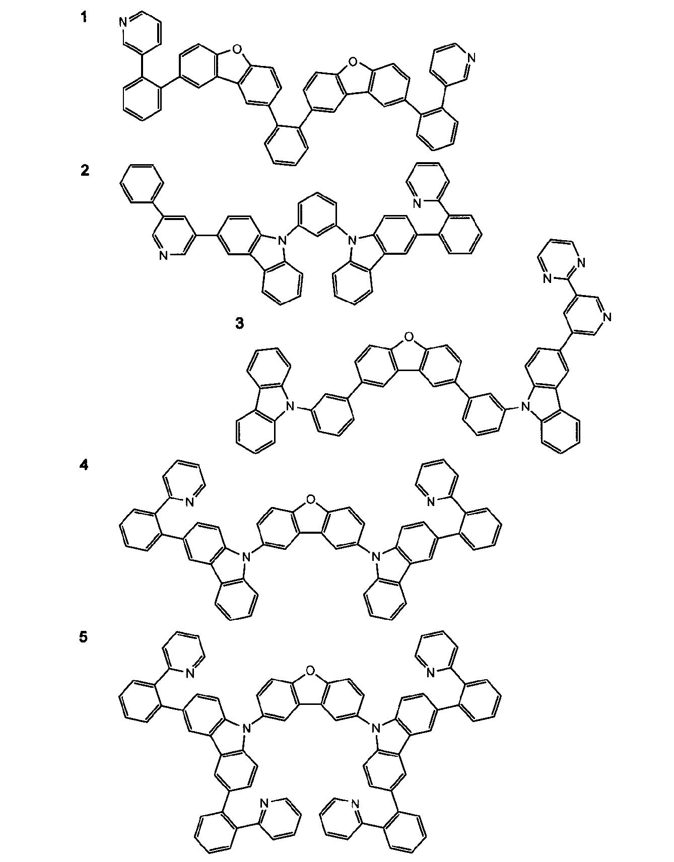


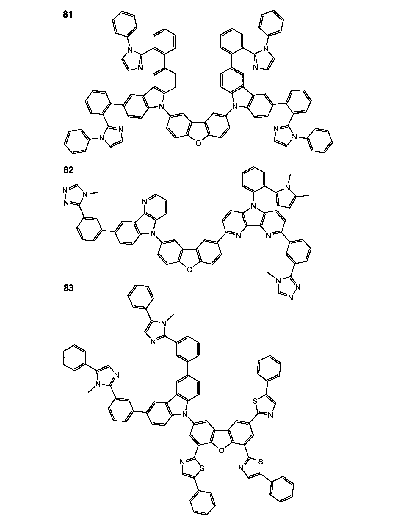


(化合物の合成例)
以下に代表的な化合物の合成例として、化合物5の具体的な合成例を示すが、これに限定されない。
(Example of compound synthesis)
Specific examples of the synthesis of compound 5 are shown below as typical synthesis examples of the compound, but are not limited thereto.

工程1:中間体1の合成
窒素雰囲気下、2,8-ジブロモジベンゾフラン(1.0モル)、カルバゾール(2.0モル)、銅粉末(3.0モル)、炭酸カリウム(1.5モル)を、DMAc(ジメチルアセトアミド)300ml中で混合し、130℃で24時間撹拌した。これによって得た反応液を室温まで冷却後、トルエン1Lを加え、蒸留水で3回洗浄し、減圧雰囲気下において洗浄物から溶媒を留去し、その残渣をシリカゲルフラッシュクロマトグラフィー(n-ヘプタン:トルエン=4:1~3:1)にて精製し、中間体1を収率85%で得た。
Step 1: Synthesis of Intermediate 1 Under a nitrogen atmosphere, 2,8-dibromodibenzofuran (1.0 mol), carbazole (2.0 mol), copper powder (3.0 mol), potassium carbonate (1.5 mol) Were mixed in 300 ml of DMAc (dimethylacetamide) and stirred at 130 ° C. for 24 hours. The reaction solution thus obtained was cooled to room temperature, 1 L of toluene was added, washed with distilled water three times, the solvent was distilled off from the washed product under a reduced pressure atmosphere, and the residue was subjected to silica gel flash chromatography (n-heptane: Purification with toluene = 4: 1 to 3: 1) gave Intermediate 1 in a yield of 85%.
工程2:中間体2の合成
室温、大気下で中間体1(0.5モル)をDMF(ジメチルホルムアミド)100mlに溶解し、NBS(N-ブロモコハク酸イミド)(2.0モル)を加え、一晩室温で撹拌した。得られた沈殿を濾過し、メタノールで洗浄し、中間体2を収率92%で得た。
Step 2: Synthesis of Intermediate 2 Intermediate 1 (0.5 mol) was dissolved in 100 ml of DMF (dimethylformamide) at room temperature and in the atmosphere, NBS (N-bromosuccinimide) (2.0 mol) was added, Stir overnight at room temperature. The resulting precipitate was filtered and washed with methanol, yielding intermediate 2 in 92% yield.
工程3:化合物5の合成
窒素雰囲気下、中間体2(0.25モル)、2-フェニルピリジン(1.0モル)、ルテニウム錯体[(η6-C6H6)RuCl2]2(0.05モル)、トリフェニルホスフィン(0.2モル)、炭酸カリウム(12モル)を、NMP(N-メチル-2-ピロリドン)3L中で混合し、140℃で一晩撹拌した。
Step 3: Synthesis of Compound 5 Under a nitrogen atmosphere, intermediate 2 (0.25 mol), 2-phenylpyridine (1.0 mol), ruthenium complex [(η 6 -C 6 H 6 ) RuCl 2 ] 2 (0 0.05 mol), triphenylphosphine (0.2 mol) and potassium carbonate (12 mol) were mixed in 3 L of NMP (N-methyl-2-pyrrolidone) and stirred at 140 ° C. overnight.
反応液を室温まで冷却後、ジクロロメタン5Lを加え、反応液を濾過した。次いで減圧雰囲気下(800Pa、80℃)において濾液から溶媒を留去し、その残渣をシリカゲルフラッシュクロマトグラフィー(CH2Cl2:Et3N=20:1~10:1)にて精製した。 After cooling the reaction solution to room temperature, 5 L of dichloromethane was added, and the reaction solution was filtered. Subsequently, the solvent was distilled off from the filtrate under reduced pressure (800 Pa, 80 ° C.), and the residue was purified by silica gel flash chromatography (CH 2 Cl 2 : Et 3 N = 20: 1 to 10: 1).
減圧雰囲気下において、精製物から溶媒を留去した後、その残渣をジクロロメタンに再び溶解し、水で3回洗浄した。洗浄によって得られた物質を無水硫酸マグネシウムで乾燥させ、減圧雰囲気下において乾燥後の物質から溶媒を留去することにより、化合物5を収率68%で得た。 In a reduced-pressure atmosphere, the solvent was distilled off from the purified product, and the residue was dissolved again in dichloromethane and washed with water three times. The material obtained by washing was dried over anhydrous magnesium sulfate, and the solvent was distilled off from the dried material in a reduced-pressure atmosphere to obtain Compound 5 in a yield of 68%.
(窒素含有層の成膜方法)
以上のような窒素含有層が基材11上に成膜されたものである場合、その成膜方法としては、塗布法、インクジェット法、コーティング法、ディップ法などのウェットプロセスを用いる方法や、蒸着法(抵抗加熱、EB法など)、スパッタ法、CVD法などのドライプロセスを用いる方法などが挙げられる。なかでも蒸着法が好ましく適用される。
(Method for forming a nitrogen-containing layer)
When the nitrogen-containing layer as described above is formed on the
特に、複数の化合物を用いて窒素含有層を成膜する場合であれば、複数の蒸着源から複数の化合物を同時に供給する共蒸着が適用される。また化合物として高分子材料を用いる場合であれば、塗布法が好ましく適用される。この場合、化合物を溶媒に溶解させた塗布液を用いる。化合物を溶解させる溶媒が限定されることはない。さらに、複数の化合物を用いて窒素含有層を成膜する場合であれば、複数の化合物を溶解させることが可能な溶媒を用いて塗布液を作製すれば良い。 Particularly, in the case of forming a nitrogen-containing layer using a plurality of compounds, co-evaporation in which a plurality of compounds are simultaneously supplied from a plurality of evaporation sources is applied. If a polymer material is used as the compound, a coating method is preferably applied. In this case, a coating solution in which the compound is dissolved in a solvent is used. The solvent in which the compound is dissolved is not limited. Furthermore, in the case of forming a nitrogen-containing layer using a plurality of compounds, a coating solution may be prepared using a solvent capable of dissolving the plurality of compounds.
[有機機能層]
有機機能層14は、アノードである第1電極13の上部に[正孔注入層/正孔輸送層/発光層/電子輸送層/電子注入層]をこの順に積層した構成を例示できるが、このうち少なくとも有機材料を用いて構成された発光層を有することが必要である。正孔注入層及び正孔輸送層は、正孔輸送性と正孔注入性とを有する正孔輸送/注入層として設けられてもよい。電子輸送層及び電子注入層は、電子輸送性と電子注入性とを有する単一層として設けられてもよい。また、これらの有機機能層14のうち、例えば電子注入層は無機材料で構成されている場合もある。
[Organic functional layer]
The organic
また、有機機能層14は、これらの層の他にも正孔阻止層や電子阻止層等が必要に応じて必要箇所に積層されていてよい。さらに、発光層は、各波長領域の発光光を発生させる各色発光層を有し、これらの各色発光層を、非発光性の中間層を介して積層させて発光層ユニットとして形成されていてもよい。中間層は、正孔阻止層、電子阻止層として機能してもよい。
In addition to these layers, the organic
[発光層]
発光層は、発光材料として例えば燐光発光化合物が含有されている。
この発光層は、電極又は電子輸送層から注入された電子と、正孔輸送層から注入された正孔とが再結合して発光する層であり、発光する部分は発光層の層内であっても発光層における隣接する層との界面であってもよい。
[Light emitting layer]
The light emitting layer contains, for example, a phosphorescent light emitting compound as a light emitting material.
This light emitting layer is a layer that emits light by recombination of electrons injected from the electrode or the electron transport layer and holes injected from the hole transport layer, and the light emitting portion is in the layer of the light emitting layer. Or the interface with the adjacent layer in a light emitting layer may be sufficient.
このような発光層としては、含まれる発光材料が発光要件を満たしていれば、その構成には特に制限はない。また、同一の発光スペクトルや発光極大波長を有する層が複数層あってもよい。この場合、各発光層間には非発光性の中間層(図示せず)を有していることが好ましい。 Such a light emitting layer is not particularly limited in its configuration as long as the light emitting material contained satisfies the light emission requirements. Moreover, there may be a plurality of layers having the same emission spectrum and emission maximum wavelength. In this case, it is preferable to have a non-light emitting intermediate layer (not shown) between the light emitting layers.
発光層の厚さの総和は1~100nmの範囲にあることが好ましく、さらに好ましくは、より低い電圧で駆動することができることから1~30nmである。尚、発光層の厚さの総和とは、発光層間に非発光性の中間層が存在する場合には、当該中間層も含む厚さである。 The total thickness of the light emitting layers is preferably in the range of 1 to 100 nm, and more preferably 1 to 30 nm because it can be driven at a lower voltage. In addition, the sum total of the thickness of a light emitting layer is the thickness also including the said intermediate | middle layer, when a nonluminous intermediate | middle layer exists between light emitting layers.
複数層を積層した構成の発光層の場合、個々の発光層の厚さとしては、1~50nmの範囲に調整することが好ましく、1~20nmの範囲に調整することがより好ましい。積層された複数の発光層が、青、緑、赤のそれぞれの発光色に対応する場合、青、緑、赤の各発光層の厚さの関係については、特に制限はない。 In the case of a light emitting layer having a structure in which a plurality of layers are laminated, the thickness of each light emitting layer is preferably adjusted to a range of 1 to 50 nm, and more preferably adjusted to a range of 1 to 20 nm. When the plurality of stacked light emitting layers correspond to the respective emission colors of blue, green, and red, there is no particular limitation on the relationship between the thicknesses of the blue, green, and red light emitting layers.
以上のような発光層は、後述する発光材料やホスト化合物を、例えば、真空蒸着法、スピンコート法、キャスト法、LB法、インクジェット法等の公知の薄膜形成方法により形成することができる。 The light emitting layer as described above can be formed of a light emitting material or a host compound, which will be described later, by a known thin film forming method such as a vacuum deposition method, a spin coating method, a casting method, an LB method, or an ink jet method.
また発光層は、複数の発光材料を混合してもよく、また燐光発光材料と蛍光発光材料(蛍光ドーパント、蛍光性化合物ともいう)を同一発光層中に混合して用いてもよい。 In the light emitting layer, a plurality of light emitting materials may be mixed, and a phosphorescent light emitting material and a fluorescent light emitting material (also referred to as a fluorescent dopant or a fluorescent compound) may be mixed and used in the same light emitting layer.
発光層の構成として、ホスト化合物(発光ホストともいう)、発光材料(発光ドーパント化合物、ゲスト材料ともいう)を含有し、発光材料より発光させることが好ましい。 The structure of the light emitting layer preferably contains a host compound (also referred to as a light emitting host) and a light emitting material (also referred to as a light emitting dopant compound or a guest material) and emits light from the light emitting material.
(ホスト化合物)
発光層に含有されるホスト化合物としては、室温(25℃)における燐光発光の燐光量子収率が0.1未満の化合物が好ましい。さらに、燐光量子収率が0.01未満である化合物が好ましい。また、ホスト化合物は、発光層に含有される化合物の中で、層中での体積比が50%以上であることが好ましい。
(Host compound)
As the host compound contained in the light emitting layer, a compound having a phosphorescence quantum yield of phosphorescence emission at room temperature (25 ° C.) of less than 0.1 is preferable. Furthermore, the compound whose phosphorescence quantum yield is less than 0.01 is preferable. The host compound preferably has a volume ratio in the layer of 50% or more among the compounds contained in the light emitting layer.
ホスト化合物としては、公知のホスト化合物を単独で用いてもよく、又は複数種用いてもよい。ホスト化合物を複数種用いることで、電荷の移動を調整することが可能であり、有機EL素子10を高効率化することができる。また、後述する発光材料を複数種用いることで、異なる発光を混ぜることが可能となり、これにより任意の発光色を得ることができる。
As the host compound, a known host compound may be used alone, or a plurality of types may be used. By using a plurality of types of host compounds, it is possible to adjust the movement of charges, and the
用いられるホスト化合物としては、従来公知の低分子化合物でも、繰り返し単位をもつ高分子化合物でもよく、ビニル基やエポキシ基のような重合性基を有する低分子化合物(蒸着重合性発光ホスト)でもよい。 The host compound used may be a conventionally known low molecular compound, a high molecular compound having a repeating unit, or a low molecular compound having a polymerizable group such as a vinyl group or an epoxy group (evaporation polymerizable light emitting host). .
公知のホスト化合物としては、正孔輸送能、電子輸送能を有しつつ、発光の長波長化を防ぎ、かつ高Tg(ガラス転移温度)化合物が好ましい。ここでいうガラス転移点(Tg)とは、DSC(Differential Scanning Colorimetry:示差走査熱量法)を用いて、JIS-K-7121に準拠した方法により求められる値である。 As the known host compound, a compound having a high Tg (glass transition temperature) that has a hole transporting ability and an electron transporting ability and prevents the emission of light from being long-wavelength is preferable. The glass transition point (Tg) here is a value obtained by a method in accordance with JIS-K-7121 using DSC (Differential Scanning Colorimetry).
有機エレクトロルミネッセンス素子に適用可能なホスト化合物としては、特開2013-4245号公報の段落[0163]~[0178]に記載の化合物H1~H79を例示することができる。特開2013-4245号公報の段落[0163]~[0178]に記載の化合物H1~H79を本願明細書に組み込む。 Examples of host compounds applicable to organic electroluminescence devices include compounds H1 to H79 described in paragraphs [0163] to [0178] of JP2013-4245A. Compounds H1 to H79 described in paragraphs [0163] to [0178] of JP2013-4245A are incorporated in the present specification.
また、その他の公知のホスト化合物の具体例としては、以下の文献に記載されている化合物を用いることもできる。例えば、特開2001-257076号公報、同2002-308855号公報、同2001-313179号公報、同2002-319491号公報、同2001-357977号公報、同2002-334786号公報、同2002-8860号公報、同2002-334787号公報、同2002-15871号公報、同2002-334788号公報、同2002-43056号公報、同2002-334789号公報、同2002-75645号公報、同2002-338579号公報、同2002-105445号公報、同2002-343568号公報、同2002-141173号公報、同2002-352957号公報、同2002-203683号公報、同2002-363227号公報、同2002-231453号公報、同2003-3165号公報、同2002-234888号公報、同2003-27048号公報、同2002-255934号公報、同2002-260861号公報、同2002-280183号公報、同2002-299060号公報、同2002-302516号公報、同2002-305083号公報、同2002-305084号公報、同2002-308837号公報等が挙げられる。 Also, as specific examples of other known host compounds, compounds described in the following documents can be used. For example, Japanese Patent Laid-Open Nos. 2001-257076, 2002-308855, 2001-313179, 2002-319491, 2001-357777, 2002-334786, 2002-8860 Gazette, 2002-334787, 2002-15871, 2002-334788, 2002-43056, 2002-334789, 2002-75645, 2002-338579 No. 2002-105445, No. 2002-343568, No. 2002-141173, No. 2002-352957, No. 2002-203683, No. 2002-363227, No. 2002-231453. No. 2003-3165, No. 2002-234888, No. 2003-27048, No. 2002-255934, No. 2002-286061, No. 2002-280183, No. 2002-299060. No. 2002-302516, No. 2002-305083, No. 2002-305084, No. 2002-308837, and the like.
(発光材料)
本実施形態の有機エレクトロルミネッセンス素子に用いることのできる発光材料としては、燐光発光性化合物(燐光性化合物、燐光発光材料ともいう)が挙げられる。
(Luminescent material)
Examples of the light-emitting material that can be used for the organic electroluminescence element of the present embodiment include phosphorescent compounds (also referred to as phosphorescent compounds and phosphorescent materials).
燐光発光性化合物とは、励起三重項からの発光が観測される化合物であり、具体的には室温(25℃)にて燐光発光する化合物であり、燐光量子収率が25℃において0.01以上の化合物であると定義されるが、好ましい燐光量子収率は0.1以上である。 A phosphorescent compound is a compound in which light emission from an excited triplet is observed. Specifically, a phosphorescent compound emits phosphorescence at room temperature (25 ° C.), and a phosphorescence quantum yield of 0.01 at 25 ° C. Although defined as the above compounds, the preferred phosphorescence quantum yield is 0.1 or more.
上記燐光量子収率は、第4版実験化学講座7の分光IIの398頁(1992年版、丸善)に記載の方法により測定できる。溶液中での燐光量子収率は種々の溶媒を用いて測定できるが、本例において燐光発光性化合物を用いる場合、任意の溶媒のいずれかにおいて上記燐光量子収率(0.01以上)が達成されればよい。 The phosphorescent quantum yield can be measured by the method described in Spectroscopic II, page 398 (1992 edition, Maruzen) of Experimental Chemistry Course 4 of the 4th edition. Although the phosphorescence quantum yield in a solution can be measured using various solvents, when the phosphorescent compound is used in this example, the phosphorescence quantum yield (0.01 or more) is achieved in any solvent. It only has to be done.
燐光発光性化合物の発光の原理としては2種挙げられる。一つは、キャリアが輸送されるホスト化合物上でキャリアの再結合が起こってホスト化合物の励起状態が生成し、このエネルギーを燐光発光性化合物に移動させることで燐光発光性化合物からの発光を得るというエネルギー移動型であり、もう一つは、燐光発光性化合物がキャリアトラップとなり、燐光発光性化合物上でキャリアの再結合が起こり燐光発光性化合物からの発光が得られるというキャリアトラップ型である。いずれの場合においても、燐光発光性化合物の励起状態のエネルギーはホスト化合物の励起状態のエネルギーよりも低いことが条件となる。 There are two types of light emission principles of phosphorescent compounds. One is that recombination of carriers occurs on the host compound to which carriers are transported to generate an excited state of the host compound, and this energy is transferred to the phosphorescent compound to obtain light emission from the phosphorescent compound. The other is a carrier trap type in which the phosphorescent compound becomes a carrier trap, and carriers are recombined on the phosphorescent compound to emit light from the phosphorescent compound. In either case, it is a condition that the excited state energy of the phosphorescent compound is lower than the excited state energy of the host compound.
燐光発光性化合物は、一般的な有機エレクトロルミネッセンス素子の発光層に使用される公知のものの中から適宜選択して用いることができるが、好ましくは元素の周期表で8~10族の金属を含有する錯体系化合物である。さらに好ましくはイリジウム化合物、オスミウム化合物、又は白金化合物(白金錯体系化合物)、希土類錯体であり、中でも最も好ましいのはイリジウム化合物である。 The phosphorescent compound can be appropriately selected from known materials used for the light emitting layer of a general organic electroluminescence device, but preferably contains a metal of group 8 to 10 in the periodic table of elements. It is a complex compound. More preferred are iridium compounds, osmium compounds, platinum compounds (platinum complex compounds), and rare earth complexes, and most preferred are iridium compounds.
本実施形態の有機エレクトロルミネッセンス素子においては、少なくとも一つの発光層に2種以上の燐光発光性化合物を含有していてもよく、発光層における燐光発光性化合物の濃度比が発光層の厚さ方向で変化していてもよい。 In the organic electroluminescence device of this embodiment, at least one light emitting layer may contain two or more types of phosphorescent compounds, and the concentration ratio of the phosphorescent compounds in the light emitting layer is the thickness direction of the light emitting layer. You may have changed.
燐光発光性化合物は好ましくは発光層の総量に対し0.1体積%以上30体積%未満である。 The phosphorescent compound is preferably 0.1% by volume or more and less than 30% by volume with respect to the total amount of the light emitting layer.
有機エレクトロルミネッセンス素子に適用可能な燐光発光性化合物としては、特開2013-4245号公報の段落[0185]~[0235]に記載の一般式(4)、一般式(5)、一般式(6)で表される化合物、及び、例示化合物を好ましく挙げることができる。また、その他の例示化合物として、Ir-46、Ir-47、Ir-48を以下に示す。特開2013-4245号公報の段落[0185]~[0235]に記載の一般式(4)、一般式(5)、一般式(6)で表される化合物、及び、例示化合物(Pt-1~Pt-3、Os-1、Ir-1~Ir-45)を本願明細書に組み込む。 As the phosphorescent compound applicable to the organic electroluminescence device, the general formulas (4), (5), and (6) described in paragraphs [0185] to [0235] of JP2013-4245A can be used. ) And exemplary compounds can be preferably mentioned. As other exemplary compounds, Ir-46, Ir-47 and Ir-48 are shown below. Compounds represented by general formula (4), general formula (5) and general formula (6) described in paragraphs [0185] to [0235] of JP2013-4245A, and exemplified compounds (Pt-1 ~ Pt-3, Os-1, Ir-1 ~ Ir-45) are incorporated herein.

なお、これらの燐光発光性化合物(燐光発光性の金属錯体ともいう)は、有機EL素子10の発光層に発光ドーパントとして含有されることが好ましい態様であるが、発光層以外の有機機能層に含有されていてもよい。
In addition, although it is preferable that these phosphorescent compounds (also referred to as phosphorescent metal complexes) are contained in the light emitting layer of the
また、燐光発光性化合物は、有機EL素子10の発光層に使用される公知のものの中から適宜選択して用いることができる。
The phosphorescent compound can be appropriately selected from known compounds used for the light emitting layer of the
上記の燐光発光性化合物(燐光発光性金属錯体等ともいう)は、例えば、Organic Letters誌 vol.3 No.16 2579~2581頁(2001)、Inorganic Chemistry,第30巻 第8号 1685~1687頁(1991年)、J.Am.Chem.Soc.,123巻 4304頁(2001年)、Inorganic Chemistry,第40巻第7号 1704~1711頁(2001年)、Inorganic Chemistry,第41巻 第12号 3055~3066頁(2002年)、New Journal of Chemistry.,第26巻 1171頁(2002年)、European Journal of Organic Chemistry,第4巻 695~709頁(2004年)、さらにこれらの文献中に記載の参考文献等の方法を適用することにより合成できる。 The above phosphorescent compounds (also referred to as phosphorescent metal complexes) are, for example, OrganicOrLetters magazine vol.3 No.16 2579-2581 (2001), Inorganic Chemistry, Vol.30, No.8 1685-1687. (1991), J. Am. Chem. Soc., 123 4304 (2001), Inorganic Chemistry, Vol. 40, No. 7, 704 1704-1711 (2001), Inorganic Chemistry, Vol. 41 No. 12 3055-3066 (2002), New Journal of 第 Chemistry., 26261171 (2002), European Journal of Organic Chemistry, Vol.4 695-709 (2004), further described in these documents Can be synthesized by applying a method such as the reference.
(蛍光発光材料)
蛍光発光材料としては、クマリン系色素、ピラン系色素、シアニン系色素、クロコニウム系色素、スクアリウム系色素、オキソベンツアントラセン系色素、フルオレセイン系色素、ローダミン系色素、ピリリウム系色素、ペリレン系色素、スチルベン系色素、ポリチオフェン系色素、又は希土類錯体系蛍光体等が挙げられる。
(Fluorescent material)
Fluorescent materials include coumarin dyes, pyran dyes, cyanine dyes, croconium dyes, squalium dyes, oxobenzanthracene dyes, fluorescein dyes, rhodamine dyes, pyrylium dyes, perylene dyes, stilbene dyes Examples thereof include dyes, polythiophene dyes, and rare earth complex phosphors.
[注入層:正孔注入層、電子注入層]
注入層とは、駆動電圧低下や発光輝度向上のために電極と発光層の間に設けられる層のことで、「有機EL素子とその工業化最前線(1998年11月30日エヌ・ティー・エス社発行)」の第2編第2章「電極材料」(123~166頁)に詳細に記載されており、正孔注入層と電子注入層とがある。
[Injection layer: hole injection layer, electron injection layer]
An injection layer is a layer provided between an electrode and a light-emitting layer in order to lower drive voltage or improve light emission luminance. “An organic EL element and its forefront of industrialization (November 30, 1998, NTS) The details are described in Chapter 2, “Electrode Materials” (pages 123 to 166) of the second edition of the “Company Issue”, and there are a hole injection layer and an electron injection layer.
注入層は、必要に応じて設けることができる。正孔注入層であれば、アノードと発光層又は正孔輸送層の間、電子注入層であればカソードと発光層又は電子輸送層との間に配置される。 The injection layer can be provided as necessary. If it is a hole injection layer, it will be arranged between the anode and the light emitting layer or hole transport layer, and if it is an electron injection layer, it will be arranged between the cathode and the light emitting layer or electron transport layer.
正孔注入層は、特開平9-45479号公報、同9-260062号公報、同8-288069号公報等にもその詳細が記載されており、具体例として、銅フタロシアニンに代表されるフタロシアニン層、酸化バナジウムに代表される酸化物層、アモルファスカーボン層、ポリアニリン(エメラルディン)やポリチオフェン等の導電性高分子を用いた高分子層等が挙げられる。 The details of the hole injection layer are described in JP-A Nos. 9-45479, 9-260062, and 8-288069. Specific examples thereof include a phthalocyanine layer represented by copper phthalocyanine. And an oxide layer typified by vanadium oxide, an amorphous carbon layer, and a polymer layer using a conductive polymer such as polyaniline (emeraldine) or polythiophene.
電子注入層は、特開平6-325871号公報、同9-17574号公報、同10-74586号公報等にもその詳細が記載されており、具体的にはストロンチウムやアルミニウム等に代表される金属層、フッ化カリウムに代表されるアルカリ金属ハライド層、フッ化マグネシウムに代表されるアルカリ土類金属化合物層、酸化モリブデンに代表される酸化物層等が挙げられる。電子注入層はごく薄い層であることが望ましく、素材にもよるがその厚さは1nm~10μmの範囲が好ましい。 The details of the electron injection layer are also described in JP-A-6-325871, JP-A-9-17574, JP-A-10-74586, and the like, and specifically, metals such as strontium and aluminum Examples thereof include an alkali metal halide layer typified by potassium fluoride, an alkaline earth metal compound layer typified by magnesium fluoride, and an oxide layer typified by molybdenum oxide. The electron injection layer is preferably a very thin layer, and the thickness is preferably in the range of 1 nm to 10 μm, although it depends on the material.
[正孔輸送層]
正孔輸送層は、正孔を輸送する機能を有する正孔輸送材料からなり、広い意味で正孔注入層、電子阻止層も正孔輸送層に含まれる。正孔輸送層は単層又は複数層設けることができる。
[Hole transport layer]
The hole transport layer is made of a hole transport material having a function of transporting holes, and in a broad sense, a hole injection layer and an electron blocking layer are also included in the hole transport layer. The hole transport layer can be provided as a single layer or a plurality of layers.
正孔輸送材料としては、正孔の注入又は輸送、電子の障壁性のいずれかを有するものであり、有機物、無機物のいずれであってもよい。例えば、トリアゾール誘導体、オキサジアゾール誘導体、イミダゾール誘導体、ポリアリールアルカン誘導体、ピラゾリン誘導体及びピラゾロン誘導体、フェニレンジアミン誘導体、アリールアミン誘導体、アミノ置換カルコン誘導体、オキサゾール誘導体、スチリルアントラセン誘導体、フルオレノン誘導体、ヒドラゾン誘導体、スチルベン誘導体、シラザン誘導体、アニリン系共重合体、また、導電性高分子オリゴマー、特にチオフェンオリゴマー等が挙げられる。 The hole transport material has any of hole injection or transport and electron barrier properties, and may be either organic or inorganic. For example, triazole derivatives, oxadiazole derivatives, imidazole derivatives, polyarylalkane derivatives, pyrazoline derivatives and pyrazolone derivatives, phenylenediamine derivatives, arylamine derivatives, amino-substituted chalcone derivatives, oxazole derivatives, styrylanthracene derivatives, fluorenone derivatives, hydrazone derivatives, Examples thereof include stilbene derivatives, silazane derivatives, aniline copolymers, and conductive polymer oligomers, particularly thiophene oligomers.
正孔輸送材料としては、上記のものを使用することができるが、ポルフィリン化合物、芳香族第3級アミン化合物及びスチリルアミン化合物、特に芳香族第3級アミン化合物を用いることが好ましい。 As the hole transport material, those described above can be used, but it is preferable to use a porphyrin compound, an aromatic tertiary amine compound and a styrylamine compound, particularly an aromatic tertiary amine compound.
芳香族第3級アミン化合物及びスチリルアミン化合物の代表例としては、N,N,N′,N′-テトラフェニル-4,4′-ジアミノフェニル;N,N′-ジフェニル-N,N′-ビス(3-メチルフェニル)-〔1,1′-ビフェニル〕-4,4′-ジアミン(TPD);2,2-ビス(4-ジ-p-トリルアミノフェニル)プロパン;1,1-ビス(4-ジ-p-トリルアミノフェニル)シクロヘキサン;N,N,N′,N′-テトラ-p-トリル-4,4′-ジアミノビフェニル;1,1-ビス(4-ジ-p-トリルアミノフェニル)-4-フェニルシクロヘキサン;ビス(4-ジメチルアミノ-2-メチルフェニル)フェニルメタン;ビス(4-ジ-p-トリルアミノフェニル)フェニルメタン;N,N′-ジフェニル-N,N′-ジ(4-メトキシフェニル)-4,4′-ジアミノビフェニル;N,N,N′,N′-テトラフェニル-4,4′-ジアミノジフェニルエーテル;4,4′-ビス(ジフェニルアミノ)クオードリフェニル;N,N,N-トリ(p-トリル)アミン;4-(ジ-p-トリルアミノ)-4′-〔4-(ジ-p-トリルアミノ)スチリル〕スチルベン;4-N,N-ジフェニルアミノ-(2-ジフェニルビニル)ベンゼン;3-メトキシ-4′-N,N-ジフェニルアミノスチルベンゼン;N-フェニルカルバゾール、さらには米国特許第5,061,569号明細書に記載されている2個の縮合芳香族環を分子内に有するもの、例えば、4,4′-ビス〔N-(1-ナフチル)-N-フェニルアミノ〕ビフェニル(NPD)、特開平4-308688号公報に記載されているトリフェニルアミンユニットが3つスターバースト型に連結された4,4′,4″-トリス〔N-(3-メチルフェニル)-N-フェニルアミノ〕トリフェニルアミン(MTDATA)等が挙げられる。 Representative examples of aromatic tertiary amine compounds and styrylamine compounds include N, N, N ′, N′-tetraphenyl-4,4′-diaminophenyl; N, N′-diphenyl-N, N′— Bis (3-methylphenyl)-[1,1′-biphenyl] -4,4′-diamine (TPD); 2,2-bis (4-di-p-tolylaminophenyl) propane; 1,1-bis (4-di-p-tolylaminophenyl) cyclohexane; N, N, N ′, N′-tetra-p-tolyl-4,4′-diaminobiphenyl; 1,1-bis (4-di-p-tolyl) Aminophenyl) -4-phenylcyclohexane; bis (4-dimethylamino-2-methylphenyl) phenylmethane; bis (4-di-p-tolylaminophenyl) phenylmethane; N, N'-diphenyl-N, N ' Di (4-methoxyphenyl) -4,4'-diaminobiphenyl; N, N, N ', N'-tetraphenyl-4,4'-diaminodiphenyl ether; 4,4'-bis (diphenylamino) quadriphenyl N, N, N-tri (p-tolyl) amine; 4- (di-p-tolylamino) -4 '-[4- (di-p-tolylamino) styryl] stilbene; 4-N, N-diphenylamino -(2-diphenylvinyl) benzene; 3-methoxy-4'-N, N-diphenylaminostilbenzene; N-phenylcarbazole, and also two described in US Pat. No. 5,061,569 Having a condensed aromatic ring of, for example, 4,4′-bis [N- (1-naphthyl) -N-phenylamino] biphenyl (NPD), JP-A-4-30 4,4 ′, 4 ″ -tris [N- (3-methylphenyl) -N-phenylamino] triphenylamine in which three triphenylamine units described in Japanese Patent No. 688 are linked in a starburst type ( MTDATA) and the like.
さらにこれらの材料を高分子鎖に導入した、又はこれらの材料を高分子の主鎖とした高分子材料を用いることもできる。また、p型-Si、p型-SiC等の無機化合物も正孔注入材料、正孔輸送材料として使用することができる。 Further, a polymer material in which these materials are introduced into a polymer chain or these materials are used as a polymer main chain can also be used. In addition, inorganic compounds such as p-type-Si and p-type-SiC can also be used as the hole injection material and the hole transport material.
また、特開平11-251067号公報、J.Huang et.al.,Applied Physics Letters,80(2002),p.139に記載されているような、いわゆるp型正孔輸送材料を用いることもできる。高効率の発光素子が得られることから、これらの材料を用いることが好ましい。 Also, so-called p-type hole transport materials as described in JP-A-11-251067, J. Huang et al., Applied Physics Letters, 80 (2002), p. 139 can be used. . These materials are preferably used because a highly efficient light-emitting element can be obtained.
正孔輸送層は、上記正孔輸送材料を、例えば、真空蒸着法、スピンコート法、キャスト法、インクジェット法を含む印刷法、LB法等の公知の方法により、薄膜化することにより形成することができる。正孔輸送層の厚さについては特に制限はないが、通常は5nm~5μm程度、好ましくは5~200nmである。この正孔輸送層は、上記材料の1種又は2種以上からなる一層構造であってもよい。 The hole transport layer is formed by thinning the hole transport material by a known method such as a vacuum deposition method, a spin coating method, a casting method, a printing method including an ink jet method, or an LB method. Can do. The thickness of the hole transport layer is not particularly limited, but is usually about 5 nm to 5 μm, preferably 5 to 200 nm. The hole transport layer may have a single layer structure composed of one or more of the above materials.
また、正孔輸送層の材料に不純物をドープしてp性を高くすることもできる。その例としては、特開平4-297076号公報、特開2000-196140号公報、同2001-102175号公報、J.Appl.Phys.,95,5773(2004)等に記載されたものが挙げられる。 It is also possible to increase the p property by doping impurities in the material of the hole transport layer. Examples thereof include those described in JP-A-4-297076, JP-A-2000-196140, 2001-102175, J. Appl. Phys., 95, 5773 (2004), and the like. .
このように、正孔輸送層のp性を高くすると、より低消費電力の素子を作製することができるため好ましい。 Thus, it is preferable to increase the p property of the hole transport layer because an element with lower power consumption can be manufactured.
[電子輸送層]
電子輸送層は、電子を輸送する機能を有する材料からなり、広い意味で電子注入層、正孔阻止層(図示せず)も電子輸送層に含まれる。電子輸送層は単層構造または複数層の積層構造として設けることができる。
[Electron transport layer]
The electron transport layer is made of a material having a function of transporting electrons, and in a broad sense, an electron injection layer and a hole blocking layer (not shown) are also included in the electron transport layer. The electron transport layer can be provided as a single layer structure or a stacked structure of a plurality of layers.
単層構造の電子輸送層、および積層構造の電子輸送層において発光層に隣接する層部分を構成する電子輸送材料(正孔阻止材料を兼ねる)としては、カソードより注入された電子を発光層に伝達する機能を有していれば良い。このような材料としては従来公知の化合物の中から任意のものを選択して用いることができる。例えば、ニトロ置換フルオレン誘導体、ジフェニルキノン誘導体、チオピランジオキシド誘導体、カルボジイミド、フレオレニリデンメタン誘導体、アントラキノジメタン、アントロン誘導体及びオキサジアゾール誘導体等が挙げられる。さらに、上記オキサジアゾール誘導体において、オキサジアゾール環の酸素原子を硫黄原子に置換したチアジアゾール誘導体、電子吸引基として知られているキノキサリン環を有するキノキサリン誘導体も、電子輸送層の材料として用いることができる。さらにこれらの材料を高分子鎖に導入した、またはこれらの材料を高分子の主鎖とした高分子材料を用いることもできる。 As an electron transport material (also serving as a hole blocking material) constituting a layer portion adjacent to the light emitting layer in the electron transport layer having a single layer structure and the electron transport layer having a multilayer structure, electrons injected from the cathode are used as the light emitting layer. What is necessary is just to have the function to transmit. As such a material, any one of conventionally known compounds can be selected and used. Examples include nitro-substituted fluorene derivatives, diphenylquinone derivatives, thiopyran dioxide derivatives, carbodiimides, fluorenylidenemethane derivatives, anthraquinodimethane, anthrone derivatives, and oxadiazole derivatives. Furthermore, in the above oxadiazole derivative, a thiadiazole derivative in which the oxygen atom of the oxadiazole ring is substituted with a sulfur atom, and a quinoxaline derivative having a quinoxaline ring known as an electron-withdrawing group can also be used as a material for the electron transport layer. it can. Furthermore, a polymer material in which these materials are introduced into a polymer chain or these materials are used as a polymer main chain can also be used.
また、8-キノリノール誘導体の金属錯体、例えば、トリス(8-キノリノール)アルミニウム(Alq3)、トリス(5,7-ジクロロ-8-キノリノール)アルミニウム、トリス(5,7-ジブロモ-8-キノリノール)アルミニウム、トリス(2-メチル-8-キノリノール)アルミニウム、トリス(5-メチル-8-キノリノール)アルミニウム、ビス(8-キノリノール)亜鉛(Znq)等、及びこれらの金属錯体の中心金属がIn、Mg、Cu、Ca、Sn、GaまたはPbに置き替わった金属錯体も、電子輸送層の材料として用いることができる。 Also, metal complexes of 8-quinolinol derivatives such as tris (8-quinolinol) aluminum (Alq3), tris (5,7-dichloro-8-quinolinol) aluminum, tris (5,7-dibromo-8-quinolinol) aluminum Tris (2-methyl-8-quinolinol) aluminum, tris (5-methyl-8-quinolinol) aluminum, bis (8-quinolinol) zinc (Znq), and the like, and the central metals of these metal complexes are In, Mg, Metal complexes replaced with Cu, Ca, Sn, Ga, or Pb can also be used as the material for the electron transport layer.
その他、メタルフリーもしくはメタルフタロシアニン、またはそれらの末端がアルキル基やスルホン酸基等で置換されているものも、電子輸送層の材料として好ましく用いることができる。また、発光層の材料としても例示されるジスチリルピラジン誘導体も電子輸送層の材料として用いることができるし、正孔注入層、正孔輸送層と同様にn型-Si、n型-SiC等の無機半導体も電子輸送層の材料として用いることができる。 In addition, metal-free or metal phthalocyanine, or those having terminal ends substituted with an alkyl group or a sulfonic acid group can be preferably used as the material for the electron transport layer. Further, distyrylpyrazine derivatives exemplified as the material for the light emitting layer can also be used as the material for the electron transport layer, and n-type-Si, n-type-SiC, etc. as well as the hole injection layer and the hole transport layer. These inorganic semiconductors can also be used as a material for the electron transport layer.
電子輸送層は、上記材料を、例えば、真空蒸着法、スピンコート法、キャスト法、インクジェット法を含む印刷法、LB法等の公知の方法により、薄膜化することにより形成することができる。電子輸送層の膜厚については特に制限はないが、通常は5nm~5μm程度、好ましくは5~200nmである。電子輸送層は上記材料の1種または2種以上からなる一層構造であってもよい。 The electron transport layer can be formed by thinning the above material by a known method such as a vacuum deposition method, a spin coating method, a casting method, a printing method including an ink jet method, or an LB method. The thickness of the electron transport layer is not particularly limited, but is usually about 5 nm to 5 μm, preferably 5 to 200 nm. The electron transport layer may have a single layer structure composed of one or more of the above materials.
また、電子輸送層に不純物をドープし、n性を高くすることもできる。その例としては、特開平4-297076号公報、同10-270172号公報、特開2000-196140号公報、同2001-102175号公報、J.Appl.Phys.,95,5773(2004)等に記載されたものが挙げられる。さらに電子輸送層には、カリウムやカリウム化合物などを含有させることが好ましい。カリウム化合物としては、例えば、フッ化カリウム等を用いることができる。このように電子輸送層のn性を高くすると、より低消費電力の素子を作製することができる。 Also, impurities can be doped in the electron transport layer to increase the n property. Examples thereof include JP-A-4-297076, JP-A-10-270172, JP-A-2000-196140, 2001-102175, J.A. Appl. Phys. 95, 5773 (2004), and the like. Furthermore, it is preferable that potassium, a potassium compound, etc. are contained in an electron carrying layer. As the potassium compound, for example, potassium fluoride can be used. Thus, when the n property of the electron transport layer is increased, an element with lower power consumption can be manufactured.
また、電子輸送層の材料(電子輸送性化合物)としては、例えば、上述の化合物No.1~No.45の窒素含有化合物、上記一般式(1)~(6)で表される構造を有する窒素含有化合物、上述の化合物1~134の窒素含有化合物を用いることが好ましい。 Further, as the material of the electron transport layer (electron transport compound), for example, the above-mentioned compound No. 1-No. It is preferable to use 45 nitrogen-containing compounds, nitrogen-containing compounds having structures represented by the above general formulas (1) to (6), and nitrogen-containing compounds of the above-mentioned compounds 1 to 134.
[阻止層:正孔阻止層、電子阻止層]
阻止層は、上述のように有機化合物薄膜の基本構成層の他に、必要に応じて設けられる。例えば、特開平11-204258号公報、同11-204359号公報、及び「有機EL素子とその工業化最前線(1998年11月30日エヌ・ティー・エス社発行)」の237頁等に記載されている正孔阻止(ホールブロック)層がある。
[Blocking layer: hole blocking layer, electron blocking layer]
As described above, the blocking layer is provided as necessary in addition to the basic constituent layer of the organic compound thin film. For example, it is described in JP-A Nos. 11-204258 and 11-204359, and “Organic EL elements and the forefront of industrialization (published by NTT Corporation on November 30, 1998)” on page 237. There is a hole blocking (hole blocking) layer.
正孔阻止層とは、広い意味では、電子輸送層の機能を有する。正孔阻止層は、電子を輸送する機能を有しつつ正孔を輸送する能力が著しく小さい正孔阻止材料からなり、電子を輸送しつつ正孔を阻止することで電子と正孔の再結合確率を向上させることができる。また、後述する電子輸送層の構成を必要に応じて、正孔阻止層として用いることができる。正孔阻止層は、発光層に隣接して設けられていることが好ましい。 The hole blocking layer has a function of an electron transport layer in a broad sense. The hole blocking layer is made of a hole blocking material that has a function of transporting electrons but has a very small ability to transport holes, and recombines electrons and holes by blocking holes while transporting electrons. Probability can be improved. Moreover, the structure of the electron carrying layer mentioned later can be used as a hole-blocking layer as needed. The hole blocking layer is preferably provided adjacent to the light emitting layer.
一方、電子阻止層とは、広い意味では、正孔輸送層の機能を有する。電子阻止層は、正孔を輸送する機能を有しつつ電子を輸送する能力が著しく小さい材料からなり、正孔を輸送しつつ電子を阻止することで電子と正孔の再結合確率を向上させることができる。また、後述する正孔輸送層の構成を必要に応じて電子阻止層として用いることができる。阻止層の厚さとしては、好ましくは3~100nmであり、さらに好ましくは5~30nmである。 On the other hand, the electron blocking layer has a function of a hole transport layer in a broad sense. The electron blocking layer is made of a material that has a function of transporting holes but has a very small ability to transport electrons, and improves the probability of recombination of electrons and holes by blocking electrons while transporting holes. be able to. Moreover, the structure of the positive hole transport layer mentioned later can be used as an electron blocking layer as needed. The thickness of the blocking layer is preferably 3 to 100 nm, and more preferably 5 to 30 nm.
[被覆中間層]
被覆中間層16は、バリア層12を有する基材11上において、第1電極13、有機機能層14及び第2電極15からなる発光積層体19が配置された以外の部分を覆うように形成されている。
[Coating intermediate layer]
The covering
被覆中間層16は、封止部材18及び封止樹脂層17と共に、第1電極13、有機機能層14及び第2電極15からなる発光積層体19を封止する部材である。このため、被覆中間層16は、この発光積層体19を劣化させる水分や酸素等の侵入を抑制する機能を有する材料を用いることが好ましい。
また、被覆中間層16は、バリア層12や封止樹脂層17に直接接する構成であるため、バリア層12や封止樹脂層17との接合性に優れた材料を用いることが好ましい。
The covering
In addition, since the covering
被覆中間層16としては、封止性が高い無機酸化物、無機窒化物、無機炭化物等の化合物により形成されることが好ましい。
具体的には、SiOx、Al2O3、In2O3、TiOx、ITO(スズ・インジウム酸化物)、AlN、Si3N4、SiOxN、TiOxN、SiC等により形成することができる。
被覆中間層16は、ゾルゲル法、蒸着法、CVD、ALD(Atomic Layer Deposition)、PVD、スパッタリング法等の公知な手法により形成可能である。
The covering
Specifically, it is formed of SiO x , Al 2 O 3 , In 2 O 3 , TiO x , ITO (tin / indium oxide), AlN, Si 3 N 4 , SiO x N, TiO x N, SiC, or the like. be able to.
The coating
また、被覆中間層16は、大気圧プラズマ法において、原料(原材料ともいう)である有機金属化合物、分解ガス、分解温度、投入電力などの条件を選択することで、酸化ケイ素、酸化ケイ素を主体とした無機酸化物、又は、無機酸窒化物や無機酸化ハロゲン化物等のような、無機炭化物、無機窒化物、無機硫化物、及び、無機ハロゲン化物等の混合物等の組成を作り分けることができる。
Further, the coating
例えば、ケイ素化合物を原料化合物として用い、分解ガスに酸素を用いれば、ケイ素酸化物が生成する。また、シラザン等を原料化合物として用いれば、酸化窒化ケイ素が生成する。これはプラズマ空間内では非常に活性な荷電粒子・活性ラジカルが高密度で存在するため、プラズマ空間内で多段階の化学反応が非常に高速に促進され、プラズマ空間内の元素が熱力学的に安定な化合物へと非常に短時間で変換されるためである。 For example, if a silicon compound is used as a raw material compound and oxygen is used as a decomposition gas, silicon oxide is generated. Further, if silazane or the like is used as a raw material compound, silicon oxynitride is generated. This is because highly active charged particles and active radicals exist in the plasma space at a high density, so that multi-step chemical reactions are accelerated very rapidly in the plasma space, and the elements in the plasma space are thermodynamically This is because it is converted into a stable compound in a very short time.
このような被覆中間層16を形成するための原料は、ケイ素化合物であれば、常温常圧下で気体、液体、固体いずれの状態であっても構わない。気体の場合にはそのまま放電空間に導入できるが、液体、固体の場合は、加熱、バブリング、減圧、超音波照射等の手段により気化させて使用する。また、溶媒によって希釈して使用してもよく、溶媒は、メタノール、エタノール、n-ヘキサン等の有機溶媒及びこれらの混合溶媒を使用できる。なお、これらの希釈溶媒は、プラズマ放電処理中において、分子状、原子状に分解されるため、影響を殆ど無視することができる。
As long as the raw material for forming such a coating
このようなケイ素化合物としては、シラン、テトラメトキシシラン、テトラエトキシシラン、テトラn-プロポキシシラン、テトライソプロポキシシラン、テトラn-ブトキシシラン、テトラt-ブトキシシラン、ジメチルジメトキシシラン、ジメチルジエトキシシラン、ジエチルジメトキシシラン、ジフェニルジメトキシシラン、メチルトリエトキシシラン、エチルトリメトキシシラン、フェニルトリエトキシシラン、(3,3,3-トリフルオロプロピル)トリメトキシシラン、ヘキサメチルジシロキサン、ビス(ジメチルアミノ)ジメチルシラン、ビス(ジメチルアミノ)メチルビニルシラン、ビス(エチルアミノ)ジメチルシラン、N,O-ビス(トリメチルシリル)アセトアミド、ビス(トリメチルシリル)カルボジイミド、ジエチルアミノトリメチルシラン、ジメチルアミノジメチルシラン、ヘキサメチルジシラザン、ヘキサメチルシクロトリシラザン、ヘプタメチルジシラザン、ノナメチルトリシラザン、オクタメチルシクロテトラシラザン、テトラキスジメチルアミノシラン、テトライソシアナートシラン、テトラメチルジシラザン、トリス(ジメチルアミノ)シラン、トリエトキシフルオロシラン、アリルジメチルシラン、アリルトリメチルシラン、ベンジルトリメチルシラン、ビス(トリメチルシリル)アセチレン、1,4-ビストリメチルシリル-1,3-ブタジイン、ジ-t-ブチルシラン、1,3-ジシラブタン、ビス(トリメチルシリル)メタン、シクロペンタジエニルトリメチルシラン、フェニルジメチルシラン、フェニルトリメチルシラン、プロパルギルトリメチルシラン、テトラメチルシラン、トリメチルシリルアセチレン、1-(トリメチルシリル)-1-プロピン、トリス(トリメチルシリル)メタン、トリス(トリメチルシリル)シラン、ビニルトリメチルシラン、ヘキサメチルジシラン、オクタメチルシクロテトラシロキサン、テトラメチルシクロテトラシロキサン、ヘキサメチルシクロテトラシロキサン、Mシリケート51等が挙げられる。 Examples of such silicon compounds include silane, tetramethoxysilane, tetraethoxysilane, tetra n-propoxysilane, tetraisopropoxysilane, tetra n-butoxysilane, tetrat-butoxysilane, dimethyldimethoxysilane, dimethyldiethoxysilane, Diethyldimethoxysilane, diphenyldimethoxysilane, methyltriethoxysilane, ethyltrimethoxysilane, phenyltriethoxysilane, (3,3,3-trifluoropropyl) trimethoxysilane, hexamethyldisiloxane, bis (dimethylamino) dimethylsilane Bis (dimethylamino) methylvinylsilane, bis (ethylamino) dimethylsilane, N, O-bis (trimethylsilyl) acetamide, bis (trimethylsilyl) carbodiimide, di Tylaminotrimethylsilane, dimethylaminodimethylsilane, hexamethyldisilazane, hexamethylcyclotrisilazane, heptamethyldisilazane, nonamethyltrisilazane, octamethylcyclotetrasilazane, tetrakisdimethylaminosilane, tetraisocyanatosilane, tetramethyldisilazane , Tris (dimethylamino) silane, triethoxyfluorosilane, allyldimethylsilane, allyltrimethylsilane, benzyltrimethylsilane, bis (trimethylsilyl) acetylene, 1,4-bistrimethylsilyl-1,3-butadiyne, di-t-butylsilane, 1,3-disilabutane, bis (trimethylsilyl) methane, cyclopentadienyltrimethylsilane, phenyldimethylsilane, phenyltrimethylsilane, Pargyltrimethylsilane, tetramethylsilane, trimethylsilylacetylene, 1- (trimethylsilyl) -1-propyne, tris (trimethylsilyl) methane, tris (trimethylsilyl) silane, vinyltrimethylsilane, hexamethyldisilane, octamethylcyclotetrasiloxane, tetramethyl Examples thereof include cyclotetrasiloxane, hexamethylcyclotetrasiloxane, M silicate 51, and the like.
また、これらケイ素を含む原料ガスを分解して被覆中間層16を得るための分解ガスとしては、水素ガス、メタンガス、アセチレンガス、一酸化炭素ガス、二酸化炭素ガス、窒素ガス、アンモニアガス、亜酸化窒素ガス、酸化窒素ガス、二酸化窒素ガス、酸素ガス、水蒸気、フッ素ガス、フッ化水素、トリフルオロアルコール、トリフルオロトルエン、硫化水素、二酸化硫黄、二硫化炭素、塩素ガス等が挙げられる。
The decomposition gas for obtaining the coating
上述のケイ素を含む原料ガスと分解ガスとを適宜選択することで、酸化ケイ素、また、窒化物、炭化物等を含有する被覆中間層16を得ることができる。
The covering
大気圧プラズマ法においては、これらの反応性ガスに対して、主にプラズマ状態になりやすい放電ガスを混合し、プラズマ放電発生装置にガスを送りこむ。このような放電ガスとしては、窒素ガス及び/又は周期表の第18属原子、具体的には、ヘリウム、ネオン、アルゴン、クリプトン、キセノン、ラドン等が用いられる。これらの中でも特に、窒素、ヘリウム、アルゴンが好ましく用いられる。 In the atmospheric pressure plasma method, these reactive gases are mixed mainly with a discharge gas that tends to be in a plasma state, and the gas is sent to a plasma discharge generator. As such a discharge gas, nitrogen gas and / or 18th group atom of the periodic table, specifically, helium, neon, argon, krypton, xenon, radon, etc. are used. Among these, nitrogen, helium, and argon are preferably used.
上記放電ガスと反応性ガスを混合し、薄膜形成(混合)ガスとして大気圧プラズマ放電発生装置(プラズマ発生装置)に供給することで膜形成を行う。放電ガスと反応性ガスの割合は、得ようとする膜の性質によって異なるが、混合ガス全体に対し、放電ガスの割合を50%以上として反応性ガスを供給する。 The film is formed by mixing the discharge gas and the reactive gas and supplying them as a thin film forming (mixed) gas to an atmospheric pressure plasma discharge generator (plasma generator). Although the ratio of the discharge gas and the reactive gas varies depending on the properties of the film to be obtained, the reactive gas is supplied with the ratio of the discharge gas being 50% or more with respect to the entire mixed gas.
[封止部材]
封止部材18は、有機EL素子10を覆うものであって、板状(フィルム状)の封止部材18が封止樹脂層17によって基材11側に固定される。この封止部材18は、有機EL素子10及び第2電極15の端子部分(図示省略)を露出させる状態で設けられている。また封止部材18に電極を設け、有機EL素子10の有機EL素子10及び第2電極15の端子部分と、この電極とを導通させるように構成されていてもよい。
[Sealing member]
The sealing
封止部材18としては、上述のバリア層12を有する基材11を封止部材18として用いることもできる。
また、封止部材18としては、樹脂フィルムがラミネート(ポリマー膜)された金属箔を用いることが好ましい。樹脂フィルムがラミネートされた金属箔は、光取りだし側の基材11として用いることはできないが、低コストであり、透湿性の低い封止材料である。このため、光取り出しを意図しない封止部材18として好適である。
As the sealing
Moreover, as the sealing
なお、金属箔とは、スパッタや蒸着等で形成された金属薄膜や、導電性ペースト等の流動性電極材料から形成された導電膜と異なり、圧延等で形成された金属の箔又はフィルムを指す。 The metal foil refers to a metal foil or film formed by rolling or the like, unlike a metal thin film formed by sputtering or vapor deposition, or a conductive film formed from a fluid electrode material such as a conductive paste. .
金属箔としては、金属の種類に特に限定はなく、例えば銅(Cu)箔、アルミニウム(Al)箔、金(Au)箔、黄銅箔、ニッケル(Ni)箔、チタン(Ti)箔、銅合金箔、ステンレス箔、スズ(Sn)箔、高ニッケル合金箔等が挙げられる。これらの各種の金属箔の中で特に好ましい金属箔としてはAl箔が挙げられる。 As metal foil, there is no limitation in particular in the kind of metal, for example, copper (Cu) foil, aluminum (Al) foil, gold (Au) foil, brass foil, nickel (Ni) foil, titanium (Ti) foil, copper alloy Examples thereof include foil, stainless steel foil, tin (Sn) foil, and high nickel alloy foil. Among these various metal foils, a particularly preferred metal foil is an Al foil.
金属箔の厚さは6~50μmが好ましい。6μm未満の場合は、金属箔に用いる材料によっては使用時にピンホールが空き、必要とするバリア性(透湿度、酸素透過率)が得られなくなる場合がある。50μmを越えた場合は、金属箔に用いる材料によってはコストの増加や、有機EL素子10が厚くなることにより、フィルム状の封止部材18を用いる利点が少なくなる場合がある。
The thickness of the metal foil is preferably 6 to 50 μm. If the thickness is less than 6 μm, depending on the material used for the metal foil, pinholes may be vacant during use, and required barrier properties (moisture permeability, oxygen permeability) may not be obtained. When the thickness exceeds 50 μm, depending on the material used for the metal foil, the advantage of using the film-shaped sealing
樹脂フィルムがラミネートされた金属箔において、樹脂フィルムとしては、機能性包装材料の新展開(株式会社 東レリサーチセンター)に記載の各種材料を用いることが可能である。例えば、ポリエチレン系樹脂、ポリプロピレン系樹脂、ポリエチレンテレフタレート系樹脂、ポリアミド系樹脂、エチレン-ビニルアルコール共重合体系樹脂、エチレン-酢酸ビニル共重合体系樹脂、アクリロニトリル-ブタジエン共重合体系樹脂、セロハン系樹脂、ビニロン系樹脂、塩化ビニリデン系樹脂等を用いることができる。ポリプロピレン系樹脂、及び、ナイロン系樹脂等の樹脂は、延伸されていてもよく、さらに塩化ビニリデン系樹脂がコートされていてもよい。また、ポリエチレン系樹脂は、低密度と高密度とのいずれを用いてもよい。 In the metal foil laminated with a resin film, various materials described in the new development of functional packaging materials (Toray Research Center, Inc.) can be used as the resin film. For example, polyethylene resin, polypropylene resin, polyethylene terephthalate resin, polyamide resin, ethylene-vinyl alcohol copolymer resin, ethylene-vinyl acetate copolymer resin, acrylonitrile-butadiene copolymer resin, cellophane resin, vinylon Resin, vinylidene chloride resin and the like can be used. A resin such as a polypropylene resin and a nylon resin may be stretched and further coated with a vinylidene chloride resin. In addition, the polyethylene resin may be either low density or high density.
また、封止部材18としては、板状又はフィルム状の基板を用いることができる。例えば、ガラス基板、ポリマー基板が挙げられ、これらの基板材料をさらに薄型のフィルム状にして用いてもよい。ガラス基板としては、特にソーダ石灰ガラス、バリウム・ストロンチウム含有ガラス、鉛ガラス、アルミノケイ酸ガラス、ホウケイ酸ガラス、バリウムホウケイ酸ガラス、石英等を挙げることができる。また、ポリマー基板としては、ポリカーボネート、アクリル、ポリエチレンテレフタレート、ポリエーテルサルファイド、ポリサルフォン等を挙げることができる。
なかでも、素子を薄型化できるということから、封止部材18として薄型のフィルム状にしたポリマー基板を使用することが好ましい。
Moreover, as the sealing
Especially, since the element can be thinned, it is preferable to use a polymer substrate in the form of a thin film as the sealing
封止部材18は、JIS-K-7126-1987に準拠した方法で測定された酸素透過度が1×10⁻³ml/(m2・24h・atm)以下、JIS-K-7129-1992に準拠した方法で測定された、水蒸気透過度(25±0.5℃、相対湿度(90±2)%RH)が1×10-3g/(m2・24h)以下であることが好ましい。
The sealing
また、以上のような基板材料は、凹板状に加工して封止部材18として用いてもよい。この場合、上述した基板部材に対してサンドブラスト加工、化学エッチング加工等の加工が施され、凹状が形成される。
Further, the above substrate material may be processed into a concave plate shape and used as the sealing
また、これに限らず、金属材料を用いてもよい。金属材料としては、ステンレス、鉄、銅、アルミニウム、マグネシウム、ニッケル、亜鉛、クロム、チタン、モリブデン、シリコン、ゲルマニウム及びタンタルからなる群から選ばれる一種以上の金属又は合金が挙げられる。このような金属材料は、薄型のフィルム状にして封止部材18として用いることにより、有機EL素子10が設けられた発光パネル全体を薄型化できる。
Further, the present invention is not limited to this, and a metal material may be used. Examples of the metal material include one or more metals or alloys selected from the group consisting of stainless steel, iron, copper, aluminum, magnesium, nickel, zinc, chromium, titanium, molybdenum, silicon, germanium, and tantalum. By using such a metal material as a sealing
[封止樹脂層]
封止部材18を基材11側に固定するための封止樹脂層17は、封止部材18と基材11とで挟持された有機EL素子10の封止に用いられる。封止樹脂層17は、例えば、アクリル酸系オリゴマー若しくはメタクリル酸系オリゴマーの反応性ビニル基を有する熱硬化性の接着剤、或いは、エポキシ系等の熱硬化性の接着剤が挙げられる。
[Sealing resin layer]
The sealing
また、封止樹脂層17の形態としては、シート状に加工された熱硬化性接着剤を用いることが好ましい。シート状の熱硬化性接着剤を用いる場合には、常温(25℃程度)では非流動性を示し、かつ、加熱すると50~130℃の範囲内の温度で流動性を発現するような接着剤(シール材)を用いる。
Further, as the form of the sealing
熱硬化性接着剤としては、任意の接着剤を使用することができる。封止樹脂層17と隣接する封止部材18や、基材11等との密着性向上の観点から、好適な熱硬化性接着剤を適宜選択する。例えば、熱硬化性接着剤としては、分子の末端または側鎖にエチレン性二重結合を有する化合物と熱重合開始剤とを主成分とする樹脂等を用いることができる。より具体的には、エポキシ系樹脂、アクリル系樹脂等からなる熱硬化性接着剤を使用することができる。また、有機EL素子10の製造工程で用いる貼合装置および硬化処理装置に応じて、溶融タイプの熱硬化性接着剤を使用してもよい。
また、接着剤として、上記した接着剤を2種以上混合したものを用いてもよいし、熱硬化性及び紫外線硬化性をともに備えた接着剤を用いてもよい。
As the thermosetting adhesive, any adhesive can be used. From the viewpoint of improving the adhesion between the sealing
Moreover, what mixed two or more types of above-mentioned adhesives may be used as an adhesive agent, and the adhesive agent provided with both thermosetting property and ultraviolet-ray-curing property may be used.
〈2.有機エレクトロルミネッセンス素子(第2実施形態:全面被覆)〉
[有機エレクトロルミネッセンス素子の構成]
次に、第2実施形態について説明する。図2に、第2実施形態の有機エレクトロルミネッセンス素子の概略構成を示す。以下にこの図に基づいて有機エレクトロルミネッセンス素子の構成を説明する。
<2. Organic Electroluminescence Element (Second Embodiment: Full Coverage)>
[Configuration of organic electroluminescence element]
Next, a second embodiment will be described. In FIG. 2, schematic structure of the organic electroluminescent element of 2nd Embodiment is shown. The configuration of the organic electroluminescence element will be described below based on this figure.
図2に示す有機EL素子20は、基材11、バリア層12、第1電極13、有機機能層14、第2電極15、被覆中間層21、封止樹脂層17、及び、封止部材18を備える。この有機EL素子20は、被覆中間層21の構成を除き、上述の第1実施形態と同様の構成である。このため以下説明では、第1実施形態の有機EL素子と同様の構成要素についての重複する詳細な説明は省略し、第2実施形態の有機EL素子の構成を説明する。
The
図2に示す有機EL素子20は、バリア層12を有する基材11上に、第1電極13、有機機能層14及び第2電極15からなる発光積層体19が配置される。そして、バリア層12、並びに、発光積層体19の側面及び上面を覆って、被覆中間層21が形成されている。さらに、被覆中間層21上に、封止樹脂層17を介して封止部材18が接合されている。
In the
この構成では、被覆中間層21が、発光積層体19(有機機能層14)の周囲のバリア層12上に形成され、さらに、バリア層12の表面から発光積層体19よりも高い位置まで形成されている。さらに、発光積層体19の上面の全面を覆うように被覆中間層21が形成されている。このため、封止部材18を接合する封止樹脂層17が、被覆中間層21上のみに接続される。
In this configuration, the covering
被覆中間層21としては、上述の第1実施形態の有機EL素子の被覆中間層と同じ材料を用いることができる。また、同じ製法により形成することができる。
被覆中間層21として、上述の無機酸化物、無機窒化物、無機炭化物等の封止性の高い材料を用いることにより、有機EL素子20の封止性がより高まる。このため、封止樹脂層17のみで封止された構成に比べて、有機EL素子20の封止性をより高めることができる。
As the covering
By using a material having high sealing properties such as the above-described inorganic oxide, inorganic nitride, and inorganic carbide as the covering
上記構成では、ポリシラザン改質層からなるバリア層12や、第1電極13、有機機能層14及び第2電極15からなる発光積層体19に、封止樹脂層17が接しない構成である。このため、封止樹脂層17に含まれる樹脂成分、有機成分、及び、フィラー等の成分と、発光積層体19との接触を被覆中間層21で遮断することができる。この結果、固体封止工程での加熱及び加圧により、封止樹脂層17に含まれる各成分との接触による、有機機能層14や第2電極15の変性や劣化を防ぐことができる。
In the above configuration, the sealing
また、一般的に、有機EL素子においては、第1電極13の形成から、有機機能層14の形成、及び、第2電極15の形成までは、真空中において一連した工程で行われる。これに対して、封止樹脂層17と封止部材18とを用いた固体封止工程は、大気中で行われる。
この場合、被覆中間層21で、発光積層体19を被覆していないと、有機機能層14や、第1電極13、第2電極15が大気に触れることになる。このため、大気中の水分や酸素等との接触により、有機機能層14や、第1電極13、第2電極15の劣化等、有機EL素子の信頼性に影響を与える可能性がある。
In general, in the organic EL element, the process from the formation of the
In this case, if the
有機EL素子20では、被覆中間層21を上述の製法により形成した場合には、第1電極13の形成から、有機機能層14の形成、第2電極15の形成、及び、被覆中間層21の形成までを、真空中において一連した工程で行うことができる。この場合には、固体封止工程においても、被覆中間層21で第1電極13、有機機能層14及び第2電極15からなる発光積層体19が覆われているため、発光積層体19が大気に曝されることがない。このため、固体封止工程の際に、第1電極13、有機機能層14及び第2電極15の劣化等を抑制することができ、有機EL素子の信頼性をより高めることができる。
In the
なお、図2に示す構成では、被覆中間層21を発光積層体19の上面よりも高い位置まで形成することで、被覆中間層21で発光積層体19を覆う構成としているが、発光積層体19を覆う被覆中間層21の構成は、上記に限られない。例えば、ALD法等の被覆性の高い製法を用いて被覆中間層21を形成することにより、発光積層体19よりも薄い被覆中間層21により、発光積層体19の側面から上面までを覆うことができる。つまり、被覆中間層21を発光積層体19より厚く形成しない構成においても、被覆中間層21により発光積層体19の側面及び上面が覆われた構成とすることができる。このような構成においても、図2に示す構成と同様の効果を得ることができる。
In the configuration shown in FIG. 2, the cover
上述の構成によれば、ポリシラザン改質層からなるバリア層12と、封止樹脂層17との間に被覆中間層21が介在することにより、封止樹脂層17の密着性が向上する。このため、封止部材18等の剥離を抑制することができる。
さらに、被覆中間層21で第1電極13、有機機能層14及び第2電極15からなる発光積層体19を覆うことにより、有機EL素子20の劣化を抑制することができる。
従って、有機EL素子の信頼性をさらに向上させることができる。
According to the above configuration, the covering
Furthermore, by covering the
Therefore, the reliability of the organic EL element can be further improved.
〈3.有機エレクトロルミネッセンス素子(第3実施形態:バリア層2層)〉
[有機エレクトロルミネッセンス素子の構成]
次に、第3実施形態について説明する。図3に、第3実施形態の有機エレクトロルミネッセンス素子の概略構成を示す。以下にこの図に基づいて有機エレクトロルミネッセンス素子の構成を説明する。
<3. Organic Electroluminescence Element (Third Embodiment: Two Barrier Layers)>
[Configuration of organic electroluminescence element]
Next, a third embodiment will be described. In FIG. 3, schematic structure of the organic electroluminescent element of 3rd Embodiment is shown. The configuration of the organic electroluminescence element will be described below based on this figure.
図3に示す有機EL素子30は、基材11、第2バリア層32、第1バリア層31、第1電極13、有機機能層14、第2電極15、被覆中間層21、封止樹脂層17、及び、封止部材18を備える。この有機EL素子30は、第1バリア層31及び第2バリア層32の構成を除き、上述の図2を用いて説明した第2実施形態と同様の構成である。このため以下説明では、第1実施形態及び第2実施形態の有機EL素子と同様の構成要素についての重複する詳細な説明は省略し、第3実施形態の有機EL素子の構成を説明する。
3 includes a
図3に示す有機EL素子30は、基材11上に、第2バリア層32が形成されている。さらに、第2バリア層32上に、第1バリア層31が形成されている。そして、第1バリア層31上に、第1電極13、有機機能層14及び第2電極15からなる発光積層体19が配置される。そして、第1バリア層31上、並びに、発光積層体19の側面及び上面を覆って、被覆中間層21が形成されている。さらに、被覆中間層21上に、封止樹脂層17を介して封止部材18が接合されている。
The
この構成では、基材11のバリア性を高める目的で、バリア層が複数形成されている。第1電極13、有機機能層14及び第2電極15からなる発光積層体19が配置される第1バリア層31は、上述のポリシラザン改質層から構成される。第2バリア層32は、ポリシラザン改質層からなる第1バリア層31と基材11との間に設けられる。
In this configuration, a plurality of barrier layers are formed for the purpose of improving the barrier property of the
このようにバリア層を複数の層から形成する場合には、バリア層の全体の厚さが10~10000nmの範囲であり、10~5000nmの範囲であることが好ましく、100~3000nmの範囲であることがより好ましく、200~2000nmの範囲であることが特に好ましい。 When the barrier layer is thus formed from a plurality of layers, the total thickness of the barrier layer is in the range of 10 to 10,000 nm, preferably in the range of 10 to 5000 nm, and in the range of 100 to 3000 nm. More preferably, the range of 200 to 2000 nm is particularly preferable.
このように、基材11とポリシラザン改質層からなる第1バリア層31との間に第2バリア層を形成することにより、基材11上に2層の積層構造のバリア層を形成することができる。また、基材11とポリシラザン改質層からなる第1バリア層31との間に、複数のバリア層を形成することにより、3層以上の積層構造としてもよい。複数層からなるバリア層を形成することにより、ポリシラザン改質層単体でバリア層を形成する場合よりも基材11に設けるバリア層のバリア性をより高めることができる。
Thus, a barrier layer having a two-layer structure is formed on the
第1バリア層31を構成するポリシラザン改質層は、上述の第1実施形態におけるバリア層と同じ材料を用いることができる。また、同じ製法により形成することができる。
The same material as that of the barrier layer in the first embodiment described above can be used for the polysilazane modified layer constituting the
第2バリア層32は、第1バリア層31と同じ材料で形成してもよく、また、異なる材料により形成してもよい。
第2バリア層32としては、樹脂フィルムの劣化をもたらす水分や酸素等素子の浸入を抑制する機能を有する材料を用いる。例えば、無機物又は有機物からなる被膜や、これらの被膜を組み合わせた第2バリア層32が形成されていることが好ましい。具体的には、酸化ケイ素、二酸化ケイ素、窒化ケイ素等を用いることができる。さらに、当該バリア性フィルムの脆弱性を改良するために、これら無機層と有機材料からなる層(有機層)の積層構造を持たせることがより好ましい。無機層と有機層の積層順については特に制限はないが、両者を交互に複数回積層させることが好ましい。
The
As the
また、第2バリア層32としては、JIS-K-7129-1992に準拠した方法で測定された、水蒸気透過度(25±0.5℃、相対湿度90±2%RH)が0.01g/(m2・24時間)以下であることが好ましい。また、JIS-K-7126-1987に準拠した方法で測定された酸素透過度が10-3ml/(m2・24時間・atm)以下、水蒸気透過度が10-5g/(m2・24時間)以下であることが好ましい。
The
バリア性フィルムの形成方法については特に限定はなく、例えば、真空蒸着法、スパッタリング法、反応性スパッタリング法、分子線エピタキシー法、クラスターイオンビーム法、イオンプレーティング法、プラズマ重合法、大気圧プラズマ重合法、プラズマCVD法、レーザーCVD法、熱CVD法、コーティング法等を用いることができる。特に、特開2004-68143号公報に記載の大気圧プラズマ重合法を好ましく用いることができる。 The method for forming the barrier film is not particularly limited. For example, the vacuum deposition method, the sputtering method, the reactive sputtering method, the molecular beam epitaxy method, the cluster ion beam method, the ion plating method, the plasma polymerization method, the atmospheric pressure plasma weight A combination method, a plasma CVD method, a laser CVD method, a thermal CVD method, a coating method, or the like can be used. In particular, the atmospheric pressure plasma polymerization method described in JP-A-2004-68143 can be preferably used.
また、第2バリア層32として好ましい形態の一例としては、厚さ方向において屈折率の分布を有し、この屈折率分布において1つ以上の極値を持つ無機膜から構成されていることが好ましい。屈折率分布において1つ以上の極値を持つ無機膜としては、ケイ素、酸素及び炭素を含む材料から構成され、ケイ素、酸素及び炭素の含有率が異なる複数の層からなる発光積層体により構成することができる。
以下、第2バリア層32に適用可能な、屈折率分布において1つ以上の極値を持つ無機膜について説明する。
Moreover, as an example of a preferable form as the
Hereinafter, an inorganic film having one or more extreme values in the refractive index distribution that can be applied to the
上記無機膜は、膜厚方向における第2バリア層32の表面からの距離と、上記各元素(ケイ素、酸素又は炭素)の原子量の比率(原子比)との関係を表す、各元素の分布曲線が下記条件を満たしていることが好ましい。
The inorganic film is a distribution curve of each element representing the relationship between the distance from the surface of the
なお、ケイ素、酸素又は炭素の原子比は、ケイ素、酸素及び炭素の各元素の合計量に対する、ケイ素、酸素又は炭素の比率[(Si,O,C)/(Si+O+C)]で表す。
ケイ素分布曲線、酸素分布曲線、及び、炭素分布曲線は、第2バリア層32の表面からの距離における、ケイ素の原子比、酸素の原子比、及び、炭素の原子比を示す。また、膜厚方向における第2バリア層32の表面(第1電極13側の界面)からの距離と、酸素と炭素との合計の原子量の比率(原子比)との関係を示す分布曲線を、酸素炭素分布曲線とする。
In addition, the atomic ratio of silicon, oxygen, or carbon is represented by the ratio [(Si, O, C) / (Si + O + C)] of silicon, oxygen, or carbon to the total amount of each element of silicon, oxygen, and carbon.
The silicon distribution curve, the oxygen distribution curve, and the carbon distribution curve indicate the atomic ratio of silicon, the atomic ratio of oxygen, and the atomic ratio of carbon at a distance from the surface of the
第2バリア層32を構成する無機膜において、ケイ素、酸素及び炭素の原子比、又は、各元素の分布曲線は、以下(i)~(iii)の条件を満たすことが好ましい。
In the inorganic film constituting the
(i)ケイ素の原子比、酸素の原子比及び炭素の原子比が、膜厚の90%以上の領域において下記式(1):
(酸素の原子比)>(ケイ素の原子比)>(炭素の原子比)・・・(1)
で表される条件を満たす。
または、ケイ素の原子比、酸素の原子比及び炭素の原子比が、膜厚の90%以上の領域において下記式(2):
(炭素の原子比)>(ケイ素の原子比)>(酸素の原子比)・・・(2)
で表される条件を満たす。
(I) In the region where the atomic ratio of silicon, the atomic ratio of oxygen and the atomic ratio of carbon are 90% or more of the film thickness, the following formula (1):
(Atomic ratio of oxygen)> (atomic ratio of silicon)> (atomic ratio of carbon) (1)
The condition represented by is satisfied.
Alternatively, in a region where the atomic ratio of silicon, the atomic ratio of oxygen, and the atomic ratio of carbon are 90% or more of the film thickness, the following formula (2):
(Atomic ratio of carbon)> (Atomic ratio of silicon)> (Atomic ratio of oxygen) (2)
The condition represented by is satisfied.
(ii)炭素分布曲線が少なくとも1つの極大値と極小値とを有する。 (Ii) The carbon distribution curve has at least one local maximum and local minimum.
(iii)炭素分布曲線における炭素の原子比の最大値及び最小値の差の絶対値が5at%以上である。 (Iii) The absolute value of the difference between the maximum value and the minimum value of the atomic ratio of carbon in the carbon distribution curve is 5 at% or more.
また、第2バリア層32を構成する無機膜としては、ケイ素、酸素及び炭素に加えて、窒素を更に含有していてもよい。窒素を含有することにより、第2バリア層32の屈折率を制御することができる。例えば、SiO2の屈折率が1.5であるのに対し、SiNの屈折率は1.8~2.0程度である。このため、第2バリア層32に窒素を含有させ。第2バリア層32内にSiONを形成することにより、好ましい屈折率の値である1.6~1.8とすることが可能となる。このように、窒素の含有量を調整することにより、第2バリア層32の屈折率を制御することが可能である。
The inorganic film constituting the
ケイ素、酸素及び炭素に加えて、窒素を含む場合、ケイ素、酸素、炭素又は窒素の原子比は、ケイ素、酸素、炭素及び窒素の各元素の合計量に対する、ケイ素、酸素、炭素又は窒素の比率[(Si,O,C,N)/(Si+O+C+N)]で表す。
ケイ素分布曲線、酸素分布曲線、炭素分布曲線、及び、窒素分布曲線は、第2バリア層32の表面からの距離における、ケイ素の原子比、酸素の原子比、炭素の原子比、及び、窒素の原子比を示す。
In the case of containing nitrogen in addition to silicon, oxygen and carbon, the atomic ratio of silicon, oxygen, carbon or nitrogen is the ratio of silicon, oxygen, carbon or nitrogen to the total amount of each element of silicon, oxygen, carbon and nitrogen [(Si, O, C, N) / (Si + O + C + N)].
The silicon distribution curve, the oxygen distribution curve, the carbon distribution curve, and the nitrogen distribution curve represent the atomic ratio of silicon, the atomic ratio of oxygen, the atomic ratio of carbon, and the nitrogen ratio at a distance from the surface of the
第2バリア層32を構成する上述の無機膜は、プラズマ化学気相成長(プラズマCVD)法により形成された層であることが好ましい。特に、基材11を一対の成膜ロール上に配置し、この一対の成膜ロール間に放電してプラズマを発生させるプラズマ化学気相成長法で形成することが好ましい。プラズマ化学気相成長法はペニング放電プラズマ方式のプラズマ化学気相成長法であってもよい。また、一対の成膜ロール間に放電する際には、一対の成膜ロールの極性を交互に反転させることが好ましい。
The above-mentioned inorganic film constituting the
プラズマ化学気相成長法においてプラズマを発生させる際には、複数の成膜ロールの間の空間にプラズマ放電を発生させることが好ましい。特に、一対の成膜ロールを用い、この一対の成膜ロールのそれぞれに基材11を配置して、一対の成膜ロール間に放電してプラズマを発生させることがより好ましい。
When plasma is generated in the plasma chemical vapor deposition method, it is preferable to generate a plasma discharge in a space between a plurality of film forming rolls. In particular, it is more preferable to use a pair of film forming rolls, dispose the
この方法では、一対の成膜ロール上に基材11を配置して、この成膜ロール間に放電することにより、一方の成膜ロール上に存在する基材11上に成膜することができる。同時に、もう一方の成膜ロール上の基材11上にも成膜することが可能である。このため、成膜レートを倍にでき、効率よく薄膜を製造できる。さらに、一対の成膜ロール上のそれぞれの基材11上に、同じ構造の膜を形成できる。
In this method, the
また、上記プラズマ化学気相成長法には有機ケイ素化合物と酸素とを含む成膜ガスを用いることが好ましい。成膜ガス中の酸素の含有量は、成膜ガス中の有機ケイ素化合物の全量を完全酸化するのに必要な理論酸素量以下であることが好ましい。
第2バリア層32を構成する無機膜は、連続的な成膜プロセスにより形成された層であることが好ましい。
In the plasma chemical vapor deposition method, a film forming gas containing an organosilicon compound and oxygen is preferably used. The oxygen content in the film forming gas is preferably less than or equal to the theoretical oxygen amount necessary for complete oxidation of the entire amount of the organosilicon compound in the film forming gas.
The inorganic film constituting the
〈4.有機エレクトロルミネッセンス素子の製造方法(第4実施形態)〉
[有機エレクトロルミネッセンス素子の製造方法]
有機エレクトロルミネッセンス素子の製造方法一例として、図1に示す有機エレクトロルミネッセンス素子10の製造方法を説明する。
<4. Method for Manufacturing Organic Electroluminescence Element (Fourth Embodiment)>
[Method of manufacturing organic electroluminescence element]
As an example of a method for manufacturing the organic electroluminescence element, a method for manufacturing the
まず、基材11上に、バリア層12を1nm~100μm程度の厚さで形成する。例えば、基材11上にポリシラザン含有液を所定の厚さに塗布する。そして、この塗布膜に、エキシマ処理を行うことでポリシラザン改質層からなるバリア層12を形成する。
なお、第3実施形態のように、複数のバリア層を有する構成の場合には、バリア層12を形成する前に、基材11上に各種のバリア層を形成する。
First, the
In the case of a configuration having a plurality of barrier layers as in the third embodiment, various barrier layers are formed on the
次に、バリア層12上に、発光積層体19を形成する。
まず、バリア層12上に、第1電極13を形成する。第1電極13は、透明な導電性材料から形成する。例えば、銀を主成分とする3nm~15nm程度の厚さの電極や、100nm程度のITO等の透明導電性物質を形成する。第1電極13の形成は、スピンコート法、キャスト法、インクジェット法、蒸着法、スパッタ法、印刷法等があるが、均質な層が得られやすく、且つピンホールが生成しにくい等の点から、真空蒸着法が特に好ましい。また、第1電極13の形成前後には、必要に応じて補助電極のパターン形成を行う。
Next, the
First, the
次に、第1電極13上に、正孔注入層、正孔輸送層、発光層、電子輸送層、電子注入層の順に形成し、有機機能層14を形成する。これらの各層の形成は、スピンコート法、キャスト法、インクジェット法、蒸着法、スパッタ法、印刷法等があるが、均質な層が得られやすく、且つピンホールが生成しにくい等の点から、真空蒸着法又はスピンコート法が特に好ましい。さらに層ごとに異なる形成方法を適用してもよい。これらの各層の形成に蒸着法を採用する場合、その蒸着条件は使用する化合物の種類等により異なるが、一般に化合物を収蔵したボート加熱温度50℃~450℃、真空度10-6Pa~10-2Pa、蒸着速度0.01nm/秒~50nm/秒、基板温度-50℃~300℃、厚さ0.1μm~5μmの範囲で、各条件を適宜選択することが望ましい。
Next, a hole injection layer, a hole transport layer, a light emitting layer, an electron transport layer, and an electron injection layer are formed in this order on the
次に、カソードとなる第2電極15を、蒸着法やスパッタ法などの適宜の形成方法によって形成する。この際、有機機能層14によって第1電極13に対して絶縁状態を保ちつつ、有機機能層14の上方から基材11の周縁に端子部分を引き出した形状にパターン形成する。
以上により、バリア層12上に発光積層体19を形成する。
Next, the
Thus, the
次に、第1電極13、有機機能層14及び第2電極15を設けていないバリア層12上、つまり、発光積層体19の周囲のバリア層12上に被覆中間層16を形成する。被覆中間層16は、例えば、大気圧プラズマ法を用いて、無機酸化物、無機窒化物、無機炭化物等の化合物を、第2電極15の上面以下の厚さで形成する。
なお、上述の第2実施形態のように、第1電極13、有機機能層14及び第2電極15を覆う被覆中間層を形成する場合には、上記製法により第2電極15上を覆う厚さ(高さ)まで、無機酸化物、無機窒化物、無機炭化物等の化合物層を形成すればよい。または、被覆性の高い製法を用いて、発光積層体19の側面及び上面を覆う被覆中間層を形成すればよい。
Next, the covering
In addition, when forming the coating intermediate layer which covers the
次に、封止樹脂層17及び封止部材18を用いて固体封止を行う。まず、封止部材18の片面に封止樹脂層17を形成する。そして、第1電極13と第2電極15の引き出し電極の端部が、封止樹脂層17の外に出るように、封止部材18の封止樹脂層17形成面を、被覆中間層16を介して、基材11上に重ね合わせる。基材11と封止部材18とを重ね合わせた後、基材11と封止部材18とに押圧をかける。さらに、封止樹脂層17を硬化するために、封止樹脂層17の硬化温度以上に加熱する。
Next, solid sealing is performed using the sealing
以上の工程により、基材11上に、ポリシラザン改質層からなるバリア層12と被覆中間層16とを備え、固体封止された有機EL素子10が得られる。このような有機EL素子10の作製においては、一回の真空引きで一貫して第1電極13から被覆中間層16まで作製するのが好ましいが、途中で真空雰囲気から取り出して異なる形成法を施しても構わない。その際、作業を乾燥不活性ガス雰囲気下で行う等の配慮が必要となる。
Through the above steps, a solid-sealed
なお、上述の各実施形態では、基材及びバリア層を備え、この上に第1電極、有機機能層及び第2電極からなる素子を設け、さらに、この素子を固体封止したボトミエミッション型の有機エレクトロルミネッセンス素子を説明している。このような有機エレクトロルミネッセンス素子は、ボトムエミッション型に限られず、例えば、第2電極側から光を取り出すトップエミッション型の構成や、両面から光を取り出す両面発光型の構成としてもよい。有機エレクトロルミネッセンス素子がトップエミッション型であれば、第2電極に透明な材料を用いて、発光光hを第2電極側から取り出す構成とする。また、有機エレクトロルミネッセンス素子が両面発光型であれば、第2電極に透明な材料を用い、発光光hを両面から取り出す構成とする。 In each of the above-described embodiments, a bottom emission type in which a substrate and a barrier layer are provided, an element including the first electrode, the organic functional layer, and the second electrode is provided thereon, and the element is solid-sealed. The organic electroluminescence element is described. Such an organic electroluminescence element is not limited to the bottom emission type, and may be, for example, a top emission type configuration in which light is extracted from the second electrode side or a dual emission type configuration in which light is extracted from both sides. If the organic electroluminescence element is a top emission type, a transparent material is used for the second electrode, and the emitted light h is extracted from the second electrode side. If the organic electroluminescence element is a double-sided light emitting type, a transparent material is used for the second electrode, and the emitted light h is extracted from both sides.
以下、実施例に基づいて本発明をより具体的に説明するが、本発明は以下の実施例に限定されるものではない。 Hereinafter, the present invention will be described more specifically based on examples, but the present invention is not limited to the following examples.
[ボトムエミッション型の有機エレクトロルミネッセンス素子の作製]
試料101~107,201~207,301~307の各有機EL素子を、発光領域の面積が5cm×5cmとなるように作製した。下記表2には試料101~107,201~207,301~307の各有機EL素子における各層の構成を示す。
[Production of bottom emission type organic electroluminescence device]
The organic EL elements of Samples 101 to 107, 201 to 207, and 301 to 307 were manufactured so that the area of the light emitting region was 5 cm × 5 cm. Table 2 below shows the configuration of each layer in each of the organic EL elements of Samples 101 to 107, 201 to 207, and 301 to 307.
[試料101の有機エレクトロルミネッセンス素子の作製手順]
試料101の作製において、まず、透明な2軸延伸ポリエチレンナフタレートフィルムの基材上に第2バリア層と第1バリア層とを順次形成し、この上に上記窒素含有層として示した化合物No.10からなる下地層と、銀からなる導電層を形成して、透光性電極を作製した。さらに、透光性電極上に、有機機能層と、対向電極を形成した後、被覆中間層を形成した。さらに、封止樹脂層と封止部材により固体封止し、試料101の有機EL素子を作製した。
[Procedure for manufacturing organic electroluminescence element of sample 101]
In the preparation of the sample 101, first, a second barrier layer and a first barrier layer were sequentially formed on a transparent biaxially stretched polyethylene naphthalate film substrate, and the compound No. 1 shown as the nitrogen-containing layer was formed thereon. A base layer made of 10 and a conductive layer made of silver were formed to produce a translucent electrode. Furthermore, an organic functional layer and a counter electrode were formed on the translucent electrode, and then a coating intermediate layer was formed. Furthermore, the organic EL element of the sample 101 was produced by solid sealing with a sealing resin layer and a sealing member.
(第2バリア層の形成)
基材をCVDロールコーター(神戸製鋼製、W35 Series)に装着して、下記製膜条件(プラズマCVD条件)にて、基材上に、ケイ素、酸素及び炭素を含み、屈折率分布において1つ以上の極値を持つ無機膜(Si,O,C)を、第2バリア層として300nmの厚さで作製した。
(Formation of second barrier layer)
The substrate is mounted on a CVD roll coater (Kobe Steel, W35 Series), and contains silicon, oxygen, and carbon on the substrate under the following film forming conditions (plasma CVD conditions), one in the refractive index distribution. An inorganic film (Si, O, C) having the above extreme values was produced as a second barrier layer with a thickness of 300 nm.
原料ガス(HMDSO)の供給量:50sccm(Standard Cubic Centimeter per Minute)
酸素ガス(O2)の供給量:500sccm
真空チャンバー内の真空度:3Pa
プラズマ発生用電源からの印加電力:1.2kW
プラズマ発生用電源の周波数:80kHz
フィルムの搬送速度:0.5m/min
Source gas (HMDSO) supply: 50 sccm (Standard Cubic Centimeter per Minute)
Supply amount of oxygen gas (O 2 ): 500 sccm
Degree of vacuum in the vacuum chamber: 3Pa
Applied power from the power source for plasma generation: 1.2 kW
Frequency of power source for plasma generation: 80 kHz
Film transport speed: 0.5 m / min
(第1バリア層の形成)
まず、ポリシラザン含有液として、パーヒドロポリシラザン(アクアミカ NN120-10、無触媒タイプ、AZエレクトロニックマテリアルズ(株)製)の10質量%ジブチルエーテル溶液を作製した。
次に、第2バリア層を形成した基材上に、ポリシラザン含有液を、ワイヤレスバーにて、乾燥後の平均膜厚が300nmとなるように塗布し、温度85℃、湿度55%RHの雰囲気下で1分間処理して乾燥させた。更に、温度25℃、湿度10%RH(露点温度-8℃)の雰囲気下に10分間保持し、除湿処理を行って、ポリシラザン層を形成した。
(Formation of the first barrier layer)
First, as a polysilazane-containing liquid, a 10% by mass dibutyl ether solution of perhydropolysilazane (Aquamica NN120-10, non-catalytic type, manufactured by AZ Electronic Materials Co., Ltd.) was prepared.
Next, the polysilazane-containing liquid is applied on the base material on which the second barrier layer is formed with a wireless bar so that the average film thickness after drying becomes 300 nm, and the temperature is 85 ° C. and the humidity is 55% RH. Treated under dry for 1 minute to dry. Further, it was kept in an atmosphere of a temperature of 25 ° C. and a humidity of 10% RH (dew point temperature −8 ° C.) for 10 minutes to perform a dehumidification treatment to form a polysilazane layer.
次に、ポリシラザン層を形成した基材を稼動ステージ上に固定し、下記紫外線装置を用いて、下記の改質処理条件で改質処理を行い、基材上にポリシラザン改質層からなる第1バリア層を形成した。
紫外線照射装置:株式会社 エム・ディ・コム製エキシマ照射装置
MODEL:MECL-M-1-200
照射波長:172nm
ランプ封入ガス:Xe
エキシマランプ光強度:130mW/cm2(172nm)
試料と光源の距離:1mm
ステージ加熱温度:70℃
照射装置内の酸素濃度:1.0%
エキシマランプ照射時間:5秒
Next, the base material on which the polysilazane layer is formed is fixed on the operation stage, and the following ultraviolet ray apparatus is used to perform the modification treatment under the following modification treatment conditions. A barrier layer was formed.
Ultraviolet irradiation device: excimer irradiation device manufactured by MCOM Co., Ltd. MODEL: MECL-M-1-200
Irradiation wavelength: 172 nm
Lamp filled gas: Xe
Excimer lamp light intensity: 130 mW / cm 2 (172 nm)
Distance between sample and light source: 1mm
Stage heating temperature: 70 ° C
Oxygen concentration in the irradiation device: 1.0%
Excimer lamp irradiation time: 5 seconds
(下地層、第1電極の形成)
次に、第1バリア層までを形成した基材を、市販の真空蒸着装置の基材ホルダーに固定し、化合物No.10をタングステン製の抵抗加熱ボートに入れ、これら基材ホルダーと加熱ボートとを真空蒸着装置の第1真空槽内に取り付けた。また、タングステン製の抵抗加熱ボートに銀(Ag)を入れ、真空蒸着装置の第2真空槽内に取り付けた。
(Formation of underlayer and first electrode)
Next, the base material on which the first barrier layer was formed was fixed to a base material holder of a commercially available vacuum deposition apparatus. 10 was put in a resistance heating boat made of tungsten, and the base material holder and the heating boat were mounted in the first vacuum chamber of the vacuum evaporation apparatus. Moreover, silver (Ag) was put into the resistance heating boat made from tungsten, and it attached in the 2nd vacuum chamber of a vacuum evaporation system.
次に、真空蒸着装置の第1真空槽を4×10⁻⁴Paまで減圧した後、化合物No.10の入った加熱ボートに通電して加熱し、蒸着速度0.1nm/秒~0.2nm/秒で第1電極の下地層を厚さ10nmで設けた。
次に、下地層まで形成した基材を真空のまま第2真空槽に移し、第2真空槽を4×10⁻⁴Paまで減圧した後、銀の入った加熱ボートを通電して加熱した。これにより、蒸着速度0.1nm/秒~0.2nm/秒で厚さ8nmの銀からなる第1電極を形成した。
Next, after reducing the pressure of the first vacuum chamber of the vacuum evaporation apparatus to 4 × 10 −4 Pa, The heating boat containing 10 was energized and heated, and the base layer of the first electrode was provided with a thickness of 10 nm at a deposition rate of 0.1 nm / second to 0.2 nm / second.
Next, the base material formed up to the base layer was transferred to the second vacuum chamber while being vacuumed, and after the pressure in the second vacuum chamber was reduced to 4 × 10 −4 Pa, the heating boat containing silver was energized and heated. Thus, a first electrode made of silver having a thickness of 8 nm was formed at a deposition rate of 0.1 nm / second to 0.2 nm / second.
(有機機能層~第2電極)
引き続き、市販の真空蒸着装置を用い、真空度1×10⁻⁴Paまで減圧した後、基材を移動させながら化合物HT-1を、蒸着速度0.1nm/秒で蒸着し、20nmの正孔輸送層(HTL)を設けた。
次に、化合物A-3(青色発光ドーパント)、化合物A-1(緑色発光ドーパント)、化合物A-2(赤色発光ドーパント)及び化合物H-1(ホスト化合物)を、化合物A-3が膜厚に対し線形に35重量%から5重量%になるように場所により蒸着速度を変化させ、化合物A-1と化合物A-2は膜厚に依存することなく各々0.2重量%の濃度になるように、蒸着速度0.0002nm/秒で、化合物H-1は64.6重量%から94.6重量%になるように場所により蒸着速度を変化させて、厚さ70nmになるよう共蒸着し発光層を形成した。
その後、化合物ET-1を膜厚30nmに蒸着して電子輸送層を形成し、更にフッ化カリウム(KF)を厚さ2nmで形成した。更に、アルミニウム100nmを蒸着して第2電極を形成した。
なお、上記化合物HT-1、化合物A-1~3、化合物H-1、及び、化合物ET-1は、以下に示す化合物である。
(Organic functional layer to second electrode)
Subsequently, the pressure was reduced to a vacuum degree of 1 × 10 −4 Pa using a commercially available vacuum deposition apparatus, and then the compound HT-1 was deposited at a deposition rate of 0.1 nm / second while moving the base material. A transport layer (HTL) was provided.
Next, compound A-3 (blue light-emitting dopant), compound A-1 (green light-emitting dopant), compound A-2 (red light-emitting dopant) and compound H-1 (host compound) are formed. On the other hand, the deposition rate was changed depending on the location so that it was linearly from 35% by weight to 5% by weight. Compound A-1 and Compound A-2 each had a concentration of 0.2% by weight without depending on the film thickness. Thus, at a deposition rate of 0.0002 nm / sec, the compound H-1 was co-deposited to a thickness of 70 nm by changing the deposition rate depending on the location so that it was 64.6 wt% to 94.6 wt%. A light emitting layer was formed.
Thereafter, Compound ET-1 was deposited to a thickness of 30 nm to form an electron transport layer, and potassium fluoride (KF) was further formed to a thickness of 2 nm. Furthermore, aluminum 100nm was vapor-deposited and the 2nd electrode was formed.
The compound HT-1, compounds A-1 to A-3, compound H-1, and compound ET-1 are the compounds shown below.

(被覆中間層の形成)
次に、第1電極、有機機能層及び第2電極を形成していない、発光積層体の周囲のバリア層上に、被覆中間層を形成した。被覆中間層は、上述の第1実施形態と同様に、第2電極の上面が露出するように、発光積層体上を除く発光積層体の周囲のバリア層上に部分的に形成した。
(Formation of coating intermediate layer)
Next, a coating intermediate layer was formed on the barrier layer around the light-emitting laminate in which the first electrode, the organic functional layer, and the second electrode were not formed. The covering intermediate layer was partially formed on the barrier layer around the light emitting laminate except for the light emitting laminate so that the upper surface of the second electrode was exposed as in the first embodiment.
まず、第2電極まで形成した試料をCVD装置へ移動した。次に、CVD装置の真空槽を4×10⁻⁴Paまで減圧した後、チャンバー内にシランガス(SiH4)、アンモニアガス(NH3)、窒素ガス(N2)及び水素ガス(H2)を導入した。このようにして、プラズマCVD法により250nmの窒化ケイ素膜を製膜し、被覆中間層を形成した。 First, the sample formed up to the second electrode was moved to the CVD apparatus. Next, after reducing the vacuum chamber of the CVD apparatus to 4 × 10 −4 Pa, silane gas (SiH 4 ), ammonia gas (NH 3 ), nitrogen gas (N 2 ), and hydrogen gas (H 2 ) are placed in the chamber. Introduced. In this way, a silicon nitride film having a thickness of 250 nm was formed by a plasma CVD method to form a coating intermediate layer.
(固体封止)
被覆中間層まで形成した試料を、ポリエチレンテレフタレート(PET)樹脂によりラミネートされたアルミニウム箔(厚さ100μm)の片面に熱硬化型の液状接着剤(エポキシ系樹脂)を厚さ30μmで塗設してある封止部材を用いて、素子の透光性電極の導電層、対向電極の引き出し電極の端部が外にでるように、封止部材の接着剤形成面と素子の有機機能層面を連続的に重ね合わせた。
(Solid sealing)
The sample formed up to the coating intermediate layer was coated with a thermosetting liquid adhesive (epoxy resin) with a thickness of 30 μm on one side of an aluminum foil (thickness of 100 μm) laminated with polyethylene terephthalate (PET) resin. Using a certain sealing member, the adhesive forming surface of the sealing member and the organic functional layer surface of the element are continuously provided so that the conductive layer of the transparent electrode of the element and the end of the lead electrode of the counter electrode are exposed to the outside. Superimposed.
次に、試料を減圧装置内に配置し、90℃で0.1MPaの減圧条件下で、重ね合わせた基材と封止部材とに押圧をかけて5分間保持した。続いて、試料を大気圧環境に戻し、さらに120℃で15分間加熱して接着剤を硬化させた。 Next, the sample was placed in a decompression device, and the laminated base material and the sealing member were pressed and held for 5 minutes under a decompression condition of 0.1 MPa at 90 ° C. Subsequently, the sample was returned to the atmospheric pressure environment and further heated at 120 ° C. for 15 minutes to cure the adhesive.
上記固体封止工程は、大気圧下、含水率1ppm以下の窒素雰囲気下で、JIS B 9920に準拠し、測定した清浄度がクラス100で、露点温度が-80℃以下、酸素濃度0.8ppm以下の大気圧で行った。なお、陽極、陰極からの引き出し配線等の形成に関する記載は省略してある。
以上の工程により、試料101の有機EL素子を作製した。
The above-mentioned solid sealing step is performed under atmospheric pressure and in a nitrogen atmosphere with a water content of 1 ppm or less in accordance with JIS B 9920. The following atmospheric pressure was performed. In addition, the description regarding formation of the lead-out wiring from an anode and a cathode is abbreviate | omitted.
Through the above steps, an organic EL element of Sample 101 was produced.
[試料102の有機エレクトロルミネッセンス素子の作製手順]
被覆中間層を、上述の第2実施形態と同様に、バリア層上、及び、発光積層体の側面及び上面を含む全面に形成した以外は、試料101と同様の手順で試料102の有機EL素子を作製した。
[Procedure for manufacturing organic electroluminescent element of sample 102]
Similar to the second embodiment described above, the organic EL element of the sample 102 is the same as the sample 101 except that the covering intermediate layer is formed on the barrier layer and on the entire surface including the side surface and the upper surface of the light emitting laminate. Was made.
[試料103の有機エレクトロルミネッセンス素子の作製手順]
被覆中間層を構成する材料を、250nmの酸化ケイ素膜とした以外は、試料101と同様の手順で試料103の有機EL素子を作製した。被覆中間層は、上述の第1実施形態と同様に、第2電極の上面が露出するように、発光積層体上を除く発光積層体の周囲のバリア層上に部分的に形成した。
[Procedure for Manufacturing Organic Electroluminescence Element of Sample 103]
An organic EL element of Sample 103 was prepared in the same procedure as Sample 101 except that the material constituting the coating intermediate layer was a 250 nm silicon oxide film. The covering intermediate layer was partially formed on the barrier layer around the light emitting laminate except for the light emitting laminate so that the upper surface of the second electrode was exposed as in the first embodiment.
まず、第2電極まで形成した試料をCVD装置へ移動した。次に、CVD装置の真空槽を4×10⁻⁴Paまで減圧した後、チャンバー内にシランガス(SiH4)、酸素(O2)、窒素ガス(N2)および水素ガス(H2)を導入した。このようにして、プラズマCVD法により200nmの酸化ケイ素膜からなる中間被覆層を形成した。 First, the sample formed up to the second electrode was moved to the CVD apparatus. Next, after reducing the vacuum chamber of the CVD apparatus to 4 × 10 −4 Pa, silane gas (SiH 4 ), oxygen (O 2 ), nitrogen gas (N 2 ), and hydrogen gas (H 2 ) are introduced into the chamber. did. In this way, an intermediate coating layer made of a 200 nm silicon oxide film was formed by plasma CVD.
[試料104の有機エレクトロルミネッセンス素子の作製手順]
被覆中間層を、上述の第2実施形態と同様に、バリア層上、及び、発光積層体の側面及び上面を含む全面に形成した以外は、試料103と同様の手順で試料104の有機EL素子を作製した。
[Procedure for manufacturing organic electroluminescent element of sample 104]
Similar to the second embodiment described above, the organic EL element of the sample 104 is the same as the sample 103 except that the coating intermediate layer is formed on the barrier layer and on the entire surface including the side surface and the upper surface of the light emitting laminate. Was made.
[試料105の有機エレクトロルミネッセンス素子の作製手順]
被覆中間層を構成する材料を、20nmの酸化アルミニウム膜とした以外は、試料101と同様の手順で試料105の有機EL素子を作製した。被覆中間層は、上述の第1実施形態と同様に、第2電極の上面が露出するように、発光積層体上を除く発光積層体の周囲のバリア層上に部分的に形成した。
[Procedure for Producing Organic Electroluminescent Element of Sample 105]
An organic EL element of Sample 105 was produced in the same procedure as Sample 101 except that the material constituting the covering intermediate layer was a 20 nm aluminum oxide film. The covering intermediate layer was partially formed on the barrier layer around the light emitting laminate except for the light emitting laminate so that the upper surface of the second electrode was exposed as in the first embodiment.
まず、第2電極まで形成した試料をPEALD装置へ移動した。次に、基材温度を80℃とし、原料としてTMA(テトラメチルアルミニウム)、酸化剤として酸素、パージガスとしてアルゴンを使用して、TMAと酸素を交互に導入するサイクルを繰り返した。このようにして、発光積層体上を除く発光積層体の周囲のバリア層上にPEALD法により20nmの酸化アルミニウム膜からなる中間被覆層を形成した。 First, the sample formed up to the second electrode was moved to the PEALD apparatus. Next, the substrate temperature was set to 80 ° C., TMA (tetramethylaluminum) was used as a raw material, oxygen was used as an oxidizing agent, and argon was used as a purge gas, and the cycle of alternately introducing TMA and oxygen was repeated. In this manner, an intermediate coating layer made of an aluminum oxide film having a thickness of 20 nm was formed on the barrier layer around the light emitting laminate except for the light emitting laminate by the PEALD method.
[試料106の有機エレクトロルミネッセンス素子の作製手順]
被覆中間層を、上述の第2実施形態と同様に、バリア層上、及び、発光積層体の側面及び上面を含む全面に形成した以外は、試料105と同様の手順で試料106の有機EL素子を作製した。中間被覆層は、ALD法を用いて、バリア層上、及び、発光積層体の側面及び上面を含む全面に、20nmの酸化アルミニウム膜からなる中間被覆層を形成した。
[Procedure for manufacturing organic electroluminescence element of sample 106]
Similar to the second embodiment described above, the organic EL element of the sample 106 is the same as the sample 105 except that the covering intermediate layer is formed on the barrier layer and on the entire surface including the side surface and the upper surface of the light emitting laminate. Was made. As the intermediate coating layer, an ALD method was used to form an intermediate coating layer composed of a 20 nm aluminum oxide film on the barrier layer and on the entire surface including the side surfaces and the top surface of the light emitting laminate.
[試料107の有機エレクトロルミネッセンス素子の作製手順]
被覆中間層を形成せずに、試料107の有機EL素子を作製した。作製手順は、上述の試料101の作製手順において、被覆中間層を形成しないことを除き、同様の手順で作製した。
[Procedure for Manufacturing Organic Electroluminescence Element of Sample 107]
An organic EL element of Sample 107 was produced without forming a coating intermediate layer. The manufacturing procedure was the same as that of the sample 101 described above except that the coating intermediate layer was not formed.
[試料201の有機エレクトロルミネッセンス素子の作製手順]
上述の試料101の手順において、第2バリア層をポリシラザン改質層とした以外は、試料101と同様の手順により試料201の有機EL素子を作製した。第2バリア層の形成は、試料101における第1バリア層と同様の方法で行った。被覆中間層は、上述の第1実施形態と同様に、第2電極の上面が露出するように、発光積層体上を除く発光積層体の周囲のバリア層上に部分的に形成した。
[Procedure for manufacturing organic electroluminescent element of sample 201]
In the procedure of the sample 101 described above, an organic EL element of the sample 201 was manufactured in the same procedure as the sample 101 except that the second barrier layer was a polysilazane modified layer. The formation of the second barrier layer was performed in the same manner as the first barrier layer in Sample 101. The covering intermediate layer was partially formed on the barrier layer around the light emitting laminate except for the light emitting laminate so that the upper surface of the second electrode was exposed as in the first embodiment.
[第2バリア層の形成]
まず、ポリシラザン含有液として、パーヒドロポリシラザン(アクアミカ NN120-10、無触媒タイプ、AZエレクトロニックマテリアルズ(株)製)の10質量%ジブチルエーテル溶液を作製した。
次に、基材上に、ポリシラザン含有液を、ワイヤレスバーにて、乾燥後の平均膜厚が300nmとなるように塗布し、温度85℃、湿度55%RHの雰囲気下で1分間処理して乾燥させた。更に、温度25℃、湿度10%RH(露点温度-8℃)の雰囲気下に10分間保持し、除湿処理を行って、ポリシラザン層を形成した。
[Formation of second barrier layer]
First, as a polysilazane-containing liquid, a 10% by mass dibutyl ether solution of perhydropolysilazane (Aquamica NN120-10, non-catalytic type, manufactured by AZ Electronic Materials Co., Ltd.) was prepared.
Next, a polysilazane-containing liquid is applied onto the substrate with a wireless bar so that the average film thickness after drying is 300 nm, and is treated for 1 minute in an atmosphere of temperature 85 ° C. and humidity 55% RH. Dried. Further, it was kept in an atmosphere of a temperature of 25 ° C. and a humidity of 10% RH (dew point temperature −8 ° C.) for 10 minutes to perform a dehumidification treatment to form a polysilazane layer.
次に、ポリシラザン層を形成した基材を稼動ステージ上に固定し、下記紫外線装置を用いて、下記の改質処理条件で改質処理を行い、基材上にポリシラザン改質層からなる第2バリア層を形成した。
紫外線照射装置:株式会社 エム・ディ・コム製エキシマ照射装置
MODEL:MECL-M-1-200
照射波長:172nm
ランプ封入ガス:Xe
エキシマランプ光強度:130mW/cm2(172nm)
試料と光源の距離:1mm
ステージ加熱温度:70℃
照射装置内の酸素濃度:1.0%
エキシマランプ照射時間:5秒
Next, the base material on which the polysilazane layer is formed is fixed on the operation stage, and the following ultraviolet ray apparatus is used to perform the modification treatment under the following modification treatment conditions. A barrier layer was formed.
Ultraviolet irradiation device: excimer irradiation device manufactured by MCOM Co., Ltd. MODEL: MECL-M-1-200
Irradiation wavelength: 172 nm
Lamp filled gas: Xe
Excimer lamp light intensity: 130 mW / cm 2 (172 nm)
Distance between sample and light source: 1mm
Stage heating temperature: 70 ° C
Oxygen concentration in the irradiation device: 1.0%
Excimer lamp irradiation time: 5 seconds
試料201では、上記方法で形成した第2バリア層上に、さらに、第1バリア層を形成する。このため、試料201は、同様のポリシラザン改質層が積層された構成のバリア層を有している。 In the sample 201, a first barrier layer is further formed on the second barrier layer formed by the above method. For this reason, the sample 201 has a barrier layer having a configuration in which similar polysilazane modified layers are laminated.
[試料202の有機エレクトロルミネッセンス素子の作製手順]
被覆中間層を、上述の第2実施形態と同様に、バリア層上、及び、発光積層体の側面及び上面を含む全面に形成した以外は、試料201と同様の手順で試料202の有機EL素子を作製した。
[Procedure for manufacturing organic electroluminescence element of sample 202]
Similar to the above-described second embodiment, the organic EL element of the sample 202 is the same as the sample 201 except that the covering intermediate layer is formed on the barrier layer and on the entire surface including the side surface and the upper surface of the light emitting laminate. Was made.
[試料203の有機エレクトロルミネッセンス素子の作製手順]
被覆中間層を構成する材料を、250nmの酸化ケイ素膜とした以外は、試料201と同様の手順で試料203の有機EL素子を作製した。酸化ケイ素膜からなる中間被覆層の形成は、試料103と同様の手順で行った。被覆中間層は、上述の第1実施形態と同様に、第2電極の上面が露出するように、発光積層体上を除く発光積層体の周囲のバリア層上に部分的に形成した。
[Procedure for manufacturing organic electroluminescent element of sample 203]
An organic EL element of Sample 203 was fabricated in the same procedure as Sample 201 except that the material constituting the coating intermediate layer was a 250 nm silicon oxide film. The formation of the intermediate coating layer made of the silicon oxide film was performed in the same procedure as in the sample 103. The covering intermediate layer was partially formed on the barrier layer around the light emitting laminate except for the light emitting laminate so that the upper surface of the second electrode was exposed as in the first embodiment.
[試料204の有機エレクトロルミネッセンス素子の作製手順]
被覆中間層を、上述の第2実施形態と同様に、バリア層上、及び、発光積層体の側面及び上面を含む全面に形成した以外は、試料203と同様の手順で試料204の有機EL素子を作製した。
[Procedure for manufacturing organic electroluminescent element of sample 204]
Similar to the above-described second embodiment, the organic EL element of the sample 204 is the same as the sample 203 except that the coating intermediate layer is formed on the barrier layer and on the entire surface including the side surface and the upper surface of the light emitting laminate. Was made.
[試料205の有機エレクトロルミネッセンス素子の作製手順]
被覆中間層を構成する材料を、20nmの酸化アルミニウム膜とした以外は、試料201と同様の手順で試料205の有機EL素子を作製した。酸化アルミニウム膜からなる中間被覆層の形成は、試料105と同様の手順で行った。被覆中間層は、上述の第1実施形態と同様に、第2電極の上面が露出するように、発光積層体上を除く発光積層体の周囲のバリア層上に部分的に形成した。
[Procedure for Manufacturing Organic Electroluminescence Element of Sample 205]
An organic EL element of Sample 205 was produced in the same procedure as Sample 201 except that the material constituting the coating intermediate layer was a 20 nm aluminum oxide film. The formation of the intermediate coating layer made of the aluminum oxide film was performed in the same procedure as in the sample 105. The covering intermediate layer was partially formed on the barrier layer around the light emitting laminate except for the light emitting laminate so that the upper surface of the second electrode was exposed as in the first embodiment.
[試料206の有機エレクトロルミネッセンス素子の作製手順]
被覆中間層を、上述の第2実施形態と同様に、バリア層上、及び、発光積層体の側面及び上面を含む全面に形成した以外は、試料205と同様の手順で試料206の有機EL素子を作製した。
[Procedure for manufacturing organic electroluminescent element of sample 206]
Similar to the above-described second embodiment, the organic EL element of the sample 206 is the same as the sample 205 except that the covering intermediate layer is formed on the barrier layer and on the entire surface including the side surface and the upper surface of the light emitting laminate. Was made.
[試料207の有機エレクトロルミネッセンス素子の作製手順]
被覆中間層を形成せずに、試料207の有機EL素子を作製した。作製手順は、上述の試料201の作製手順において、被覆中間層を形成しないことを除き、同様の手順で作製した。
[Procedure for Producing Organic Electroluminescent Element of Sample 207]
An organic EL element of Sample 207 was produced without forming a covering intermediate layer. The manufacturing procedure was the same as that of the sample 201 described above except that the coating intermediate layer was not formed.
[試料301の有機エレクトロルミネッセンス素子の作製手順]
上述の試料101の作製手順において、第2バリア層を形成しないことを除き、試料101と同様の手順により試料301の有機EL素子を作製した。つまり、基材上に第1バリア層のみを形成して試料301の有機EL素子を作製した。第1バリア層の形成は、試料101における第1バリア層の形成と同様の方法により行った。被覆中間層は、上述の第1実施形態と同様に、第2電極の上面が露出するように、発光積層体上を除く発光積層体の周囲のバリア層上に部分的に形成した。
[Procedure for manufacturing organic electroluminescence element of sample 301]
An organic EL element of Sample 301 was manufactured by the same procedure as Sample 101 except that the second barrier layer was not formed in the above-described Sample 101 manufacturing procedure. That is, only the first barrier layer was formed on the base material to produce the organic EL element of Sample 301. The formation of the first barrier layer was performed by the same method as the formation of the first barrier layer in Sample 101. The covering intermediate layer was partially formed on the barrier layer around the light emitting laminate except for the light emitting laminate so that the upper surface of the second electrode was exposed as in the first embodiment.
[試料302の有機エレクトロルミネッセンス素子の作製手順]
被覆中間層を、上述の第2実施形態と同様に、バリア層上、及び、発光積層体の側面及び上面を含む全面に形成した以外は、試料301と同様の手順で試料302の有機EL素子を作製した。
[Procedure for manufacturing organic electroluminescent element of sample 302]
Similar to the second embodiment described above, the organic EL element of the sample 302 is the same as the sample 301 except that the covering intermediate layer is formed on the barrier layer and on the entire surface including the side surface and the upper surface of the light emitting laminate. Was made.
[試料303の有機エレクトロルミネッセンス素子の作製手順]
被覆中間層を構成する材料を、250nmの酸化ケイ素膜とした以外は、試料301と同様の手順で試料303の有機EL素子を作製した。酸化ケイ素膜からなる中間被覆層の形成は、試料103と同様の手順で行った。被覆中間層は、上述の第1実施形態と同様に、第2電極の上面が露出するように、発光積層体上を除く発光積層体の周囲のバリア層上に部分的に形成した。
[Procedure for manufacturing organic electroluminescence element of sample 303]
An organic EL element of Sample 303 was prepared in the same procedure as Sample 301, except that the material constituting the coating intermediate layer was a 250 nm silicon oxide film. The formation of the intermediate coating layer made of the silicon oxide film was performed in the same procedure as in the sample 103. The covering intermediate layer was partially formed on the barrier layer around the light emitting laminate except for the light emitting laminate so that the upper surface of the second electrode was exposed as in the first embodiment.
[試料304の有機エレクトロルミネッセンス素子の作製手順]
被覆中間層を、上述の第2実施形態と同様に、バリア層上、及び、発光積層体の側面及び上面を含む全面に形成した以外は、試料303と同様の手順で試料304の有機EL素子を作製した。
[Procedure for Manufacturing Organic Electroluminescence Element of Sample 304]
Similar to the above-described second embodiment, the organic EL element of the sample 304 is the same as the sample 303 except that the covering intermediate layer is formed on the barrier layer and on the entire surface including the side surface and the upper surface of the light emitting laminate. Was made.
[試料305の有機エレクトロルミネッセンス素子の作製手順]
被覆中間層を構成する材料を、20nmの酸化アルミニウム膜とした以外は、試料301と同様の手順で試料305の有機EL素子を作製した。酸化アルミニウム膜からなる中間被覆層の形成は、試料105と同様の手順で行った。被覆中間層は、上述の第1実施形態と同様に、第2電極の上面が露出するように、発光積層体上を除く発光積層体の周囲のバリア層上に部分的に形成した。
[Procedure for manufacturing organic electroluminescence element of sample 305]
An organic EL element of Sample 305 was fabricated in the same procedure as Sample 301, except that the material constituting the coating intermediate layer was a 20 nm aluminum oxide film. The formation of the intermediate coating layer made of the aluminum oxide film was performed in the same procedure as in the sample 105. The covering intermediate layer was partially formed on the barrier layer around the light emitting laminate except for the light emitting laminate so that the upper surface of the second electrode was exposed as in the first embodiment.
[試料306の有機エレクトロルミネッセンス素子の作製手順]
被覆中間層を、上述の第2実施形態と同様に、バリア層上、及び、発光積層体の側面及び上面を含む全面に形成した以外は、試料305と同様の手順で試料306の有機EL素子を作製した。
[Procedure for manufacturing organic electroluminescent element of sample 306]
Similar to the second embodiment described above, the organic EL element of the sample 306 is the same as the sample 305 except that the covering intermediate layer is formed on the barrier layer and on the entire surface including the side surface and the upper surface of the light emitting laminate. Was made.
[試料307の有機エレクトロルミネッセンス素子の作製手順]
被覆中間層を形成せずに、試料307の有機EL素子を作製した。作製手順は、上述の試料301の作製手順において、被覆中間層を形成しないことを除き、同様の手順で作製した。
[Procedure for Manufacturing Organic Electroluminescence Element of Sample 307]
An organic EL element of Sample 307 was produced without forming a coating intermediate layer. The manufacturing procedure was the same as that of the sample 301 described above except that the coating intermediate layer was not formed.
[有機エレクトロルミネッセンス素子の評価]
(屈曲耐性)
屈曲耐性は、室温下、発光面と封止面とに、それぞれ屈曲直径30mmφの曲率がかかるように各試料を折り曲げ、封止部材が剥がれた際の折り曲げ回数を評価した。
1:1~50回
2:51~100回
3:101~200回
4:201~300回
5:301以上折り曲げても剥がれない
[Evaluation of organic electroluminescence device]
(Bending resistance)
The bending resistance was evaluated by bending each sample at room temperature so that the light emitting surface and the sealing surface each had a curvature with a bending diameter of 30 mmφ and the sealing member was peeled off.
1: 1 to 50 times 2:51 to 100 times 3: 101 to 200 times 4: 201 to 300 times 5: 301 or more
(保存性:ダークスポット発生率)
ダークスポット(以下DS)は有機EL素子上に形成される非発光点であり、バリア基材の持ち込み水分、バリア基材を透過してEL層へ侵入する水分、封止部材の持ち込み水分等が原因となり形成される。各試料に対して下記条件下で環境試験を行うことで、DSの発生率を調べた。
(Preservation: Dark spot occurrence rate)
A dark spot (hereinafter referred to as DS) is a non-light emitting point formed on an organic EL element, and includes moisture brought into the barrier base material, moisture penetrating the barrier base material and entering the EL layer, and moisture brought into the sealing member. Cause and form. The occurrence rate of DS was examined by conducting an environmental test on each sample under the following conditions.
各試料を、85℃85%RHの環境下、24時間保持した。その後、この各試料について、定電圧電源を用いて点灯し、ダークスポット(非発光部)面積の発生割合(発生率、初期DS発生率)を調べた。なお、ダークスポット発生率は、各試料の有機EL素子の発光面を撮影し、その画像データに対して所定の画像処理を施すことにより求めた。
測定したダークスポット発生率を、下記の5段階の判断基準に基づいて判別し、各試料の保存性を評価した。
5:ダークスポット発生率が1%以下
4:ダークスポット発生率が1%より大きく3%未満
3:ダークスポット発生率が3%以上5%未満
2:ダークスポット発生率が5%以上10%未満
1:ダークスポット発生率が10%以上
Each sample was kept in an environment of 85 ° C. and 85% RH for 24 hours. Thereafter, each sample was turned on using a constant voltage power source, and the occurrence rate (occurrence rate, initial DS occurrence rate) of the dark spot (non-light emitting portion) area was examined. The dark spot occurrence rate was obtained by photographing the light emitting surface of the organic EL element of each sample and applying predetermined image processing to the image data.
The measured dark spot occurrence rate was discriminated based on the following five-stage criteria, and the preservability of each sample was evaluated.
5: Dark spot occurrence rate is 1% or less 4: Dark spot occurrence rate is greater than 1% and less than 3% 3: Dark spot occurrence rate is 3% or more and less than 5% 2: Dark spot occurrence rate is 5% or more and less than 10% 1: Dark spot incidence is 10% or more
上記試料101~107,201~207,301~307の有機EL素子の構成、及び、各評価結果を表2に示す。 Table 2 shows the configurations of the organic EL elements of the samples 101 to 107, 201 to 207, and 301 to 307, and the evaluation results.

表2に示すように、被覆中間層を設けた試料101~106,201~206,301~306は、被覆中間層を設けなかった試料107,207,307に比べて、屈曲耐性が向上している。従って、被覆中間層を形成することにより、封止樹脂層の密着性が向上し、封止部材の剥離を抑制することができる。 As shown in Table 2, the bending resistance of the samples 101 to 106, 201 to 206, and 301 to 306 provided with the coating intermediate layer is improved compared to the samples 107, 207, and 307 without the coating intermediate layer. Yes. Therefore, by forming the covering intermediate layer, the adhesion of the sealing resin layer can be improved and the peeling of the sealing member can be suppressed.
さらに、被覆中間層として窒化シリコン膜を形成した試料は、他の試料に比べて屈曲耐性試験で良好な結果が得られた。そして、酸化シリコン膜を形成した試料が、窒化シリコン膜の次に良好な結果が得られた。この結果から、被覆中間層としては、無機窒化物を形成することが好ましいことがわかる。 Furthermore, the sample in which the silicon nitride film was formed as the covering intermediate layer had a better result in the bending resistance test than the other samples. The sample on which the silicon oxide film was formed obtained the next best result after the silicon nitride film. From this result, it is understood that it is preferable to form an inorganic nitride as the covering intermediate layer.
また、被覆中間層として、CVD法で窒化シリコン膜、酸化シリコン膜を形成した試料は、ALD法により酸化アルミニウム膜を形成した試料よりも屈曲耐性が向上している。この結果から、被覆中間層として、CVD法で形成した膜を用いることが好ましいことがわかる。 In addition, a sample in which a silicon nitride film and a silicon oxide film are formed as a coating intermediate layer by a CVD method has improved bending resistance than a sample in which an aluminum oxide film is formed by an ALD method. From this result, it can be seen that it is preferable to use a film formed by the CVD method as the covering intermediate layer.
また、第2バリア層を設けた試料101~107,201~207は、第2バリア層を設けていない試料301~307に比べて、保存性が向上している。この結果から、複数のバリア層を積層することにより、基材のバリア性を向上し、有機EL素子の信頼性が向上することがわかる。 In addition, the samples 101 to 107 and 201 to 207 provided with the second barrier layer have improved storability as compared with the samples 301 to 307 not provided with the second barrier layer. From this result, it can be seen that by laminating a plurality of barrier layers, the barrier property of the base material is improved and the reliability of the organic EL element is improved.
さらに、第2バリア層として、プラズマCVD法によりケイ素、酸素及び炭素を含み、屈折率分布において1つ以上の極値を持つ無機膜を形成した試料101~107は、第2バリア層としてポリシラザン改質層を形成した試料201~207に比べて、保存性が向上している。
従って、第2バリア層として上記無機膜を有することにより、基材のバリア性を向上することがわかる。また、同じ材料を積層したバリア層よりも、異なる材料を積層したバリア層の方がバリア性を向上することがわかる。
Further, samples 101 to 107, in which an inorganic film containing silicon, oxygen, and carbon and having one or more extreme values in the refractive index distribution is formed as the second barrier layer by plasma CVD, are used as the second barrier layer. The storage stability is improved as compared with the samples 201 to 207 in which the quality layer is formed.
Therefore, it turns out that the barrier property of a base material is improved by having the said inorganic film as a 2nd barrier layer. It can also be seen that a barrier layer in which different materials are laminated improves the barrier property over a barrier layer in which the same material is laminated.
なお、本発明は上述の実施形態例において説明した構成に限定されるものではなく、その他本発明構成を逸脱しない範囲において種々の変形、変更が可能である。 The present invention is not limited to the configuration described in the above embodiment, and various modifications and changes can be made without departing from the configuration of the present invention.
10,20,30・・・有機エレクトロルミネッセンス(EL)素子、11・・・基材、12・・・バリア層、13・・・第1電極、14・・・有機機能層、15・・・第2電極、16,21・・・被覆中間層、17・・・封止樹脂層、18・・・封止部材、19・・・発光積層体、31・・・第1バリア層、32・・・第2バリア層
DESCRIPTION OF
Claims (8)
前記可撓性基材上に設けられた、ポリシラザン改質層からなるバリア層と、
前記バリア層上に配置された、対となる電極間に少なくとも1層の発光層を有する有機機能層が設けられた積層体と、
少なくとも前記積層体の周囲の前記バリア層上に形成された被覆中間層と、
前記被覆中間層上に、前記封止樹脂層を介して接合された前記封止部材と、を備える
有機エレクトロルミネッセンス素子。 An organic electroluminescence element solid-sealed by a flexible substrate and a sealing member bonded to the flexible substrate with a sealing resin layer,
A barrier layer comprising a polysilazane modified layer provided on the flexible substrate;
A laminate in which an organic functional layer having at least one light emitting layer is provided between a pair of electrodes disposed on the barrier layer;
A coating intermediate layer formed on at least the barrier layer around the laminate;
An organic electroluminescence device comprising: the sealing member bonded to the covering intermediate layer via the sealing resin layer.
前記バリア層上に、対となる電極と、前記電極間に少なくとも1層の発光層を有する有機機能層とを積層して積層体を形成する工程と、
前記積層体の周囲の前記バリア層上に、被覆中間層を形成する工程と、
封止樹脂層を塗布し、封止部材により固体封止する工程と、を有する
有機エレクトロルミネッセンス素子の製造方法。 Forming a barrier layer on the flexible substrate;
A step of forming a laminate by laminating a pair of electrodes and an organic functional layer having at least one light emitting layer between the electrodes on the barrier layer;
Forming a coating intermediate layer on the barrier layer around the laminate;
Applying a sealing resin layer, and solid-sealing with a sealing member. A method for producing an organic electroluminescent element.
Priority Applications (5)
| Application Number | Priority Date | Filing Date | Title |
|---|---|---|---|
| CN201480012721.2A CN105027672B (en) | 2013-03-08 | 2014-03-07 | Organic electroluminescent element and method for manufacturing organic electroluminescent element |
| KR1020157024154A KR20150127071A (en) | 2013-03-08 | 2014-03-07 | Organic electroluminescent element and method of manufacturing organic electroluminescent element |
| US14/770,254 US20160005997A1 (en) | 2013-03-08 | 2014-03-07 | Organic electroluminescent element and method of manufacturing organic electroluminescent element |
| JP2015504459A JP6432505B2 (en) | 2013-03-08 | 2014-03-07 | ORGANIC ELECTROLUMINESCENT ELEMENT AND METHOD FOR PRODUCING ORGANIC ELECTROLUMINESCENT ELEMENT |
| KR1020187031182A KR102024499B1 (en) | 2013-03-08 | 2014-03-07 | Organic electroluminescent element and method of manufacturing organic electroluminescent element |
Applications Claiming Priority (2)
| Application Number | Priority Date | Filing Date | Title |
|---|---|---|---|
| JP2013046994 | 2013-03-08 | ||
| JP2013-046994 | 2013-03-08 |
Publications (1)
| Publication Number | Publication Date |
|---|---|
| WO2014136969A1 true WO2014136969A1 (en) | 2014-09-12 |
Family
ID=51491476
Family Applications (1)
| Application Number | Title | Priority Date | Filing Date |
|---|---|---|---|
| PCT/JP2014/056064 Ceased WO2014136969A1 (en) | 2013-03-08 | 2014-03-07 | Organic electroluminescent element and method of manufacturing organic electroluminescent element |
Country Status (5)
| Country | Link |
|---|---|
| US (1) | US20160005997A1 (en) |
| JP (1) | JP6432505B2 (en) |
| KR (2) | KR102024499B1 (en) |
| CN (1) | CN105027672B (en) |
| WO (1) | WO2014136969A1 (en) |
Cited By (4)
| Publication number | Priority date | Publication date | Assignee | Title |
|---|---|---|---|---|
| JP2016115602A (en) * | 2014-12-17 | 2016-06-23 | コニカミノルタ株式会社 | Organic electroluminescent element and method for manufacturing the same |
| JP2016119355A (en) * | 2014-12-19 | 2016-06-30 | コニカミノルタ株式会社 | Organic electroluminescent element |
| JP2016181373A (en) * | 2015-03-24 | 2016-10-13 | パイオニア株式会社 | Light emitting device |
| CN115668515A (en) * | 2020-06-11 | 2023-01-31 | 松下知识产权经营株式会社 | Solar cell module |
Families Citing this family (3)
| Publication number | Priority date | Publication date | Assignee | Title |
|---|---|---|---|---|
| JP2017105013A (en) * | 2015-12-08 | 2017-06-15 | 株式会社リコー | Gas barrier laminate, semiconductor device, display element, display device and system |
| JP7117681B2 (en) * | 2018-03-30 | 2022-08-15 | 日亜化学工業株式会社 | Light-emitting module manufacturing method and light-emitting module |
| CN109994649B (en) * | 2019-04-09 | 2021-08-27 | 京东方科技集团股份有限公司 | Flexible display panel, preparation method thereof and display device |
Citations (3)
| Publication number | Priority date | Publication date | Assignee | Title |
|---|---|---|---|---|
| JP2007059209A (en) * | 2005-08-24 | 2007-03-08 | Toyota Industries Corp | Electroluminescence panel and method for manufacturing the same |
| JP2012076386A (en) * | 2010-10-04 | 2012-04-19 | Konica Minolta Holdings Inc | Ultraviolet-shieldable film and organic electronic device obtained by using the same |
| JP2012250181A (en) * | 2011-06-03 | 2012-12-20 | Konica Minolta Holdings Inc | Method of manufacturing barrier film and electronic device |
Family Cites Families (12)
| Publication number | Priority date | Publication date | Assignee | Title |
|---|---|---|---|---|
| US6528824B2 (en) * | 2000-06-29 | 2003-03-04 | Semiconductor Energy Laboratory Co., Ltd. | Light emitting device |
| EP1325093A2 (en) * | 2000-09-26 | 2003-07-09 | Matsushita Electric Industrial Co., Ltd. | Display unit and drive system thereof and an information display unit |
| US20040227197A1 (en) * | 2003-02-28 | 2004-11-18 | Shinji Maekawa | Composition of carbon nitride, thin film transistor with the composition of carbon nitride, display device with the thin film transistor, and manufacturing method thereof |
| JP3915734B2 (en) * | 2003-05-12 | 2007-05-16 | ソニー株式会社 | Vapor deposition mask, display device manufacturing method using the same, and display device |
| JP4698310B2 (en) * | 2005-07-11 | 2011-06-08 | 富士フイルム株式会社 | Gas barrier film, substrate film and organic electroluminescence device |
| KR100659765B1 (en) * | 2005-09-08 | 2006-12-19 | 삼성에스디아이 주식회사 | Organic light emitting display device and manufacturing method |
| WO2008032526A1 (en) * | 2006-09-15 | 2008-03-20 | Konica Minolta Holdings, Inc. | Process for production of flexible sealing film and organic electroluminescent devices made by using the film |
| KR100918402B1 (en) * | 2008-02-01 | 2009-09-24 | 삼성모바일디스플레이주식회사 | Organic light emitting display device and manufacturing method thereof |
| JP5585267B2 (en) | 2009-08-26 | 2014-09-10 | コニカミノルタ株式会社 | Gas barrier film, method for producing the same, and organic photoelectric conversion element using the same |
| JP2012084305A (en) * | 2010-10-08 | 2012-04-26 | Sumitomo Chemical Co Ltd | Organic el device |
| JP2012084306A (en) * | 2010-10-08 | 2012-04-26 | Sumitomo Chemical Co Ltd | Organic el device |
| JP5533585B2 (en) * | 2010-11-18 | 2014-06-25 | コニカミノルタ株式会社 | Gas barrier film manufacturing method, gas barrier film, and electronic device |
-
2014
- 2014-03-07 WO PCT/JP2014/056064 patent/WO2014136969A1/en not_active Ceased
- 2014-03-07 JP JP2015504459A patent/JP6432505B2/en active Active
- 2014-03-07 KR KR1020187031182A patent/KR102024499B1/en active Active
- 2014-03-07 CN CN201480012721.2A patent/CN105027672B/en active Active
- 2014-03-07 US US14/770,254 patent/US20160005997A1/en not_active Abandoned
- 2014-03-07 KR KR1020157024154A patent/KR20150127071A/en not_active Ceased
Patent Citations (3)
| Publication number | Priority date | Publication date | Assignee | Title |
|---|---|---|---|---|
| JP2007059209A (en) * | 2005-08-24 | 2007-03-08 | Toyota Industries Corp | Electroluminescence panel and method for manufacturing the same |
| JP2012076386A (en) * | 2010-10-04 | 2012-04-19 | Konica Minolta Holdings Inc | Ultraviolet-shieldable film and organic electronic device obtained by using the same |
| JP2012250181A (en) * | 2011-06-03 | 2012-12-20 | Konica Minolta Holdings Inc | Method of manufacturing barrier film and electronic device |
Cited By (4)
| Publication number | Priority date | Publication date | Assignee | Title |
|---|---|---|---|---|
| JP2016115602A (en) * | 2014-12-17 | 2016-06-23 | コニカミノルタ株式会社 | Organic electroluminescent element and method for manufacturing the same |
| JP2016119355A (en) * | 2014-12-19 | 2016-06-30 | コニカミノルタ株式会社 | Organic electroluminescent element |
| JP2016181373A (en) * | 2015-03-24 | 2016-10-13 | パイオニア株式会社 | Light emitting device |
| CN115668515A (en) * | 2020-06-11 | 2023-01-31 | 松下知识产权经营株式会社 | Solar cell module |
Also Published As
| Publication number | Publication date |
|---|---|
| US20160005997A1 (en) | 2016-01-07 |
| KR20180120796A (en) | 2018-11-06 |
| CN105027672A (en) | 2015-11-04 |
| JP6432505B2 (en) | 2018-12-05 |
| KR102024499B1 (en) | 2019-09-23 |
| JPWO2014136969A1 (en) | 2017-02-16 |
| KR20150127071A (en) | 2015-11-16 |
| CN105027672B (en) | 2017-11-10 |
Similar Documents
| Publication | Publication Date | Title |
|---|---|---|
| JP6332032B2 (en) | Translucent electrode and electronic device | |
| US10355236B2 (en) | Transparent electrode and electronic device | |
| JP6119740B2 (en) | Method for producing transparent conductive film, transparent conductive film, and electronic device | |
| US9419241B2 (en) | Organic electroluminescent element | |
| JP6432505B2 (en) | ORGANIC ELECTROLUMINESCENT ELEMENT AND METHOD FOR PRODUCING ORGANIC ELECTROLUMINESCENT ELEMENT | |
| EP2890221A1 (en) | Transparent electrode, electronic device, and method for manufacturing transparent electrode | |
| WO2016143660A1 (en) | Organic electroluminescent element | |
| JPWO2014188913A1 (en) | Transparent electrode and electronic device | |
| JP6390613B2 (en) | Organic electroluminescence device | |
| WO2017056553A1 (en) | Organic electroluminescent element and lighting device provided with same | |
| US9818962B2 (en) | Organic electroluminescent element and method for manufacturing same | |
| JP6107825B2 (en) | Organic electroluminescence device | |
| JP6286890B2 (en) | Method for producing gas barrier film, method for producing organic electroluminescence element | |
| JP2016170879A (en) | Organic electroluminescent element | |
| WO2014181640A1 (en) | Light-emitting element and display device | |
| WO2016174950A1 (en) | Organic electroluminescent element | |
| JPWO2014208449A1 (en) | Organic electroluminescence device and method for manufacturing the same | |
| JP2016219126A (en) | Transparent electrode and organic electroluminescent element |
Legal Events
| Date | Code | Title | Description |
|---|---|---|---|
| WWE | Wipo information: entry into national phase |
Ref document number: 201480012721.2 Country of ref document: CN |
|
| 121 | Ep: the epo has been informed by wipo that ep was designated in this application |
Ref document number: 14759899 Country of ref document: EP Kind code of ref document: A1 |
|
| ENP | Entry into the national phase |
Ref document number: 2015504459 Country of ref document: JP Kind code of ref document: A |
|
| WWE | Wipo information: entry into national phase |
Ref document number: 14770254 Country of ref document: US |
|
| ENP | Entry into the national phase |
Ref document number: 20157024154 Country of ref document: KR Kind code of ref document: A |
|
| NENP | Non-entry into the national phase |
Ref country code: DE |
|
| 122 | Ep: pct application non-entry in european phase |
Ref document number: 14759899 Country of ref document: EP Kind code of ref document: A1 |