WO2011132701A1 - Wireless communication system - Google Patents
Wireless communication system Download PDFInfo
- Publication number
- WO2011132701A1 WO2011132701A1 PCT/JP2011/059709 JP2011059709W WO2011132701A1 WO 2011132701 A1 WO2011132701 A1 WO 2011132701A1 JP 2011059709 W JP2011059709 W JP 2011059709W WO 2011132701 A1 WO2011132701 A1 WO 2011132701A1
- Authority
- WO
- WIPO (PCT)
- Prior art keywords
- wireless
- communication system
- wireless communication
- electrode
- metal body
- Prior art date
- Legal status (The legal status is an assumption and is not a legal conclusion. Google has not performed a legal analysis and makes no representation as to the accuracy of the status listed.)
- Ceased
Links
Images




Classifications
-
- G—PHYSICS
- G06—COMPUTING OR CALCULATING; COUNTING
- G06K—GRAPHICAL DATA READING; PRESENTATION OF DATA; RECORD CARRIERS; HANDLING RECORD CARRIERS
- G06K19/00—Record carriers for use with machines and with at least a part designed to carry digital markings
- G06K19/06—Record carriers for use with machines and with at least a part designed to carry digital markings characterised by the kind of the digital marking, e.g. shape, nature, code
- G06K19/067—Record carriers with conductive marks, printed circuits or semiconductor circuit elements, e.g. credit or identity cards also with resonating or responding marks without active components
- G06K19/07—Record carriers with conductive marks, printed circuits or semiconductor circuit elements, e.g. credit or identity cards also with resonating or responding marks without active components with integrated circuit chips
- G06K19/077—Constructional details, e.g. mounting of circuits in the carrier
- G06K19/07749—Constructional details, e.g. mounting of circuits in the carrier the record carrier being capable of non-contact communication, e.g. constructional details of the antenna of a non-contact smart card
-
- H—ELECTRICITY
- H01—ELECTRIC ELEMENTS
- H01Q—ANTENNAS, i.e. RADIO AERIALS
- H01Q1/00—Details of, or arrangements associated with, antennas
- H01Q1/12—Supports; Mounting means
- H01Q1/22—Supports; Mounting means by structural association with other equipment or articles
- H01Q1/2208—Supports; Mounting means by structural association with other equipment or articles associated with components used in interrogation type services, i.e. in systems for information exchange between an interrogator/reader and a tag/transponder, e.g. in Radio Frequency Identification [RFID] systems
-
- H—ELECTRICITY
- H01—ELECTRIC ELEMENTS
- H01Q—ANTENNAS, i.e. RADIO AERIALS
- H01Q7/00—Loop antennas with a substantially uniform current distribution around the loop and having a directional radiation pattern in a plane perpendicular to the plane of the loop
-
- G—PHYSICS
- G08—SIGNALLING
- G08B—SIGNALLING SYSTEMS, e.g. PERSONAL CALLING SYSTEMS; ORDER TELEGRAPHS; ALARM SYSTEMS
- G08B21/00—Alarms responsive to a single specified undesired or abnormal condition and not otherwise provided for
- G08B21/02—Alarms for ensuring the safety of persons
- G08B21/0202—Child monitoring systems using a transmitter-receiver system carried by the parent and the child
- G08B21/0241—Data exchange details, e.g. data protocol
- G08B21/0247—System arrangements wherein the alarm criteria uses signal strength
Definitions
- the present invention relates to a radio communication system, and more particularly to a radio communication system using an RFID (Radio Frequency Identification) system using a radio IC device and a reader / writer.
- RFID Radio Frequency Identification
- a reader / writer that generates an induction electromagnetic field and an IC chip (also referred to as an IC tag or a wireless IC chip) that stores predetermined information attached to an article or a container are communicated in a non-contact manner.
- RFID systems that transmit information have been developed.
- the IC chip can be communicated with a reader / writer by being coupled with an antenna, that is, a radiation plate.
- This sensor switch includes an antenna coil connected to an opening / closing element and an IC module that operates with electric power from the antenna coil and wirelessly communicates with the outside.
- this sensor switch requires an opening / closing element separately from the IC module and is expensive, and requires electric power to operate the opening / closing element. Therefore, the antenna coil is enlarged. In order to read information from the IC module after being written in the module, there is a problem that transmission of the opening / closing information is slow.
- an object of the present invention is to provide a wireless communication system using a wireless IC device which is small in size and can be manufactured at low cost, is a power saving type, and has a high information transmission speed.
- a wireless communication system includes: A wireless IC device for processing a predetermined wireless signal; A reader / writer for exchanging wireless signals with the wireless IC device; A wireless communication system comprising: The wireless IC device includes a wireless IC element and a radiator, The wireless IC device is fixed to a first object, and the reader / writer detects the proximity / separation between the wireless IC device and the second object accompanying the proximity / separation of the first object and the second object; It is characterized by.
- the directivity characteristics of the wireless IC device change when approaching a second object including a metal body, etc., so that the power / information transmission path capable of communicating with the reader / writer when both approach each other Is formed.
- the radiator receives a signal from the reader / writer, and this received signal is supplied to the wireless IC device.
- the wireless IC device emits a response signal, and this response signal is emitted from the radiator to the reader / writer.
- Such communication is possible when the first object and the second object are close to each other, for example, when a door or a window is closed. If the door or window is opened, communication is impossible or breaking bad.
- the proximity / separation between the first object and the second object may be detected based on the strength (level difference) of the response signal. Thus, security can be managed.
- a security system can be constructed with a wireless IC device and a second object including a metal body.
- the wireless IC device has a simple configuration, can be manufactured at low cost, and uses a signal from the reader / writer as power, saving power.
- the signal is exchanged directly with the wireless IC device, the information transmission speed is extremely rapid.
- this wireless IC device 1A is used for UHF band communication, and includes a wireless IC element 50, a rectangular parallelepiped insulator substrate 20, and a radiator (loop electrode 30). It consists of The wireless IC element 50 processes a high-frequency signal having a predetermined frequency, and details thereof will be described below with reference to FIGS.
- the insulator substrate 20 is made of a thermosetting resin such as epoxy, a thermoplastic resin such as polyimide, or a ceramic such as LTCC (may be a dielectric or magnetic material).
- the loop electrode 30 includes surface electrodes 31 and 32 disposed on the surface of the insulating substrate 20, a back surface electrode 33 disposed on the back surface, and side electrodes 34 connecting the electrodes 31 and 33 and the electrodes 32 and 33, respectively. It consists of End portions of the surface electrodes 31 and 32 facing each other are connected to the wireless IC element 50 (power supply portions 31a and 32a).
- Each of the electrodes 31 to 34 of the loop electrode 30 is a thin film electrode pattern made of a metal foil such as copper or aluminum, or a thick film electrode pattern made of a conductive paste containing powder such as silver or copper. Is formed on the surface.
- a wireless IC element 50 is coupled to the power feeding units 31a and 32a.
- This coupling is electromagnetic coupling or direct electrical coupling (DC connection) by solder bumps.
- the wireless IC element 50 and the power feeding units 31a and 32a may be electrically connected via an electromagnetic field.
- the wireless IC device 1A having the above configuration, when a predetermined high-frequency signal is transmitted from the wireless IC element 50 to the loop electrode 30, a high-frequency current flows through the loop electrode 30, and the communication distance of the loop electrode 30 is compared. Functions as a short magnetic field antenna.
- a metal body (not shown) comes close to the back surface electrode 33 of the loop electrode 30, a magnetic field loop is formed in a direction opposite to the metal body. That is, since the loop surface which is the current circulating surface of the loop electrode 30 is positioned perpendicular to the plane of the metal body, the magnetic field H is generated in parallel to the surface of the metal body. Since magnetic field loops cannot be formed in the direction, magnetic field loops are concentrated and formed in the direction opposite to the metal body.
- the electric field E induced by the magnetic field loop is also formed in the opposite direction to the metal body. That is, the loop electrode 30 functions as an antenna element, and electromagnetic waves are radiated from the antenna element in the normal direction on the surface of the metal body. In this way, when the metal body is brought close, energy can be concentrated in the direction opposite to the metal body, so that a large gain can be obtained in the direction opposite to the metal body. That is, the directivity can be changed. The large gain enables communication between the wireless IC device 1A and the reader / writer.
- the high frequency signal radiated from the reader / writer of the RFID system and received by the loop electrode 30 is supplied to the wireless IC element 50, and the wireless IC element 50 operates.
- the response signal from the wireless IC element 50 is transmitted to the loop electrode 30 and radiated to the reader / writer.
- the reader / writer is preferably arranged in the normal direction of the surface of the metal body so that the above-described electromagnetic wave can be easily received.
- the loop electrode 30 has a predetermined length from the power feeding portion 31a to the electrodes 31, 34, 33, 34, 32 and the power feeding portion 32a on the loop surface, and has a predetermined resonance frequency corresponding to this electrical length. And matching between the impedance of the wireless IC device 1A and the impedance of the loop electrode 30 (radiating element) itself.
- the loop electrode 30 when the metal body is separated from the back electrode 33 of the loop electrode 30, a magnetic field loop is formed also in the direction in which the metal body is present, and the directivity is weakened by dispersing the magnetic field energy. Therefore, when viewed from the reader / writer, the loop electrode 30 only functions as a weak radiating element as the wireless IC device 1A, and communication with the reader / writer becomes impossible or communication at a low radiation level is performed. .
- Figure 2 shows a specific example.
- the wireless IC device 1A shown in FIG. 1 is attached to the frame 61 (first object) of the door 60 (second object), and the door 60 is a metal body.
- FIG. 2A when the door 60 is closed, the wireless IC device 1A and the door 60 (metal body) are close to each other, and communication between the wireless IC device 1A and the reader / writer becomes possible.
- FIG. 2B when the door 60 is opened, communication becomes impossible or defective. Thereby, the open / closed state of the door 60 and the window can be detected.
- a metal body may be attached or embedded in a portion where the wireless IC device 1A is close.
- the wireless IC device 1 ⁇ / b> A is fixed to the frame body 61 on the side electrode 34 side, and is arranged so that the back electrode 33 side faces the door 60.
- a reader / writer (not shown) is disposed on the surface electrodes 31 and 32 side of the wireless IC device 1A.
- a reader / writer 82 that interlocks with a computer 81 is provided in a room 80.
- the reader / writer 82 includes a transmission / reception antenna 83.
- the wireless IC device 1 ⁇ / b> A may be attached to the door frame 61, the window frame 64, and the pedestals 66 and 68 as the first object that is a device in the room.
- the metal body as the second object may be the door 60 itself, the window sash 63 itself, the safe 65 itself, or the product 67 itself. If the product 67 is a non-metal body, the metal body may be attached to a portion of the pedestal 68 where the wireless IC device 1A is close. The arrangement relationship between the wireless IC device 1A and the metal body may be reversed.
- the computer 81 detects that the door 60 is closed and the safe 65 is in a predetermined position, for example. On the other hand, if the wireless IC device 1A does not respond or the response level is equal to or less than a certain value, the computer 81 detects that the door 60 has been opened and the safe 65 has moved. Thus, the security of the room 80 can be managed. The same applies to other apparatus products.
- the wireless IC element 50 may be a wireless IC chip 51 that processes a high frequency signal as shown in FIG. 4, or a resonant circuit having a predetermined resonance frequency with the wireless IC chip 51 as shown in FIG. It may be comprised with the electric power feeding circuit board 65 containing.
- the wireless IC chip 51 shown in FIG. 4 includes a clock circuit, a logic circuit, a memory circuit, and the like, and necessary information is stored in the memory.
- the wireless IC chip 51 is provided with input / output terminal electrodes 52 and 52 and mounting terminal electrodes 53 and 53 on the back surface thereof.
- the input / output terminal electrodes 52 and 52 are electrically connected to the power feeding portions 31a and 32a through metal bumps or the like.
- Au, solder, etc. can be used as a material of a metal bump.
- the wireless IC element 50 when the wireless IC element 50 includes the wireless IC chip 51 and the power supply circuit board 65, various power supply circuits (including resonance circuits / matching circuits) may be provided on the power supply circuit board 65.
- the feeder circuit 66 includes inductance elements L1 and L2 which have mutually different inductance values and are magnetically coupled in opposite phases to each other (indicated by mutual inductance M). May be.
- the power feeding circuit 66 has a predetermined resonance frequency, and aims at impedance matching between the impedance of the wireless IC chip 51 and a nearby metal body.
- the wireless IC chip 51 and the power feeding circuit 66 may be electrically connected (DC connection) or may be coupled via an electromagnetic field.
- the power feeding circuit 66 transmits a high frequency signal having a predetermined frequency transmitted from the wireless IC chip 51 to the loop electrode 30 and supplies the received high frequency signal to the wireless IC chip 51 through the loop electrode 30. To do.
- the power feeding circuit 66 has a predetermined resonance frequency.
- the frequency of the signal transmitted / received by the loop electrode 30 may be substantially determined by the resonance frequency of the power feeding circuit 66. This facilitates impedance matching, and the electrical length of the impedance matching circuit, that is, the loop electrode 30, can be shortened.
- the input / output terminal electrode 52 of the wireless IC chip 51 is provided on the power supply terminal electrodes 142a and 142b formed on the power supply circuit board 65, and the mounting terminal electrode 53 is provided on the mounting terminal electrodes 143a and 143b.
- the input / output terminal electrode 52 of the wireless IC chip 51 is provided on the power supply terminal electrodes 142a and 142b formed on the power supply circuit board 65, and the mounting terminal electrode 53 is provided on the mounting terminal electrodes 143a and 143b.
- the power supply circuit board 65 is obtained by laminating, pressing and firing ceramic sheets 141a to 141h made of a dielectric or magnetic material.
- the insulating layer constituting the power supply circuit board 65 is not limited to the ceramic sheet, and may be a thermosetting resin such as a liquid crystal polymer or a resin sheet such as a thermoplastic resin.
- power supply terminal electrodes 142a and 142b, mounting terminal electrodes 143a and 143b, and via-hole conductors 144a, 144b, 145a, and 145b are formed on the uppermost sheet 141a.
- wiring electrodes 146a and 146b constituting the inductance elements L1 and L2 are formed, and via hole conductors 147a, 147b, 148a and 148b are formed as necessary. ing.
- the inductance element L1 in which the wiring electrode 146a is spirally connected by the via-hole conductor 147a is formed, and the inductance in which the wiring electrode 146b is spirally connected by the via-hole conductor 147b.
- Element L2 is formed.
- a capacitance is formed between the wiring electrodes 146a and 146b.
- the end 146a-1 of the wiring electrode 146a on the sheet 141b is connected to the power supply terminal electrode 142a via the via hole conductor 145a, and the end 146a-2 of the wiring electrode 146a on the sheet 141h is connected via the via hole conductors 148a and 145b. Connected to the power supply terminal electrode 142b.
- the end 146b-1 of the wiring electrode 146b on the sheet 141b is connected to the power supply terminal electrode 142b via the via hole conductor 144b, and the end 146b-2 of the wiring electrode 146b on the sheet 141h is connected via the via hole conductors 148b and 144a. Connected to the power supply terminal electrode 142a.
- the inductance elements L1 and L2 are magnetically coupled to each other and are wound in opposite directions, so that the magnetic fields passing through the inner diameters of the inductance elements L1 and L2 are opposite to each other. Therefore, the magnetic field formed by the inductance elements L1 and L2 is a closed magnetic circuit. Further, in order to obtain a desired inductance value, the wiring electrodes 146a and 146b need to be lengthened to some extent. This reduces energy loss and broadens the bandwidth near the resonance frequency.
- the inductance elements L1 and L2 are formed at different positions on the left and right when the feeder circuit board 65 is seen through the plane.
- the magnetic fields generated by the inductance elements L1 and L2 are opposite to each other.
- the resonance / matching circuit By incorporating the resonance / matching circuit in the power supply circuit board 65, characteristic fluctuations due to the influence of external articles can be suppressed, and deterioration in communication quality can be prevented. Further, if the wireless IC chip 51 constituting the wireless IC element 50 is arranged toward the center in the thickness direction of the power supply circuit board 65, the wireless IC chip 51 can be prevented from being broken, and the machine as the wireless IC element 50 can be prevented. Strength can be improved.
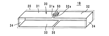
- the wireless IC device 1 ⁇ / b> B as the second example has a slit portion 35 formed in the center portion of the back electrode 33 of the loop electrode 30.
- the basic operational effects of the second example are the same as those of the first example.
- the loop electrode 30 and the metal body are close to each other, the slit portion 35 formed on the back electrode 33 of the loop electrode 30 is capacitively coupled to the adjacent metal body, and two capacitive coupling portions with the metal body are formed.
- the loop electrode 30 forms a loop.
- the loop electrode may be capacitively coupled via the slit portion 35.
- the coupling with the metal body is the same as in the first example, and the wireless IC device 1B and the reader / writer can communicate with each other by the adjacent metal body. That is, when the metal body is close, energy can be concentrated in the opposite direction to the metal body and a large gain can be obtained, so that communication with the reader / writer becomes possible.
- the loop electrode 30 and the metal body are separated from each other, the loop electrode 30 is separated by the slit portion 35. Thereby, the impedance matching function of the loop electrode 30 is lost, and the impedance of the wireless IC element 50 and the impedance of the loop electrode 30 cannot be matched. As a result, the loop electrode 30 does not function as a magnetic field antenna. Therefore, in the second example, there is a clear difference in the state of communication with the reader / writer between when the metal body is close and when it is separated, and the detection is reliable.
- the wireless IC device 1 ⁇ / b> C as the third example has the power feeding portions 31 a and 32 a with the wireless IC element 50 arranged close to one side, and the other side is omitted by the side electrode and coupled with the capacitor C. It is a thing.
- the basic effect of the third example is the same as that of the first example. In this way, the loop electrode 30 itself may be coupled by the capacitor C to form a loop.
- the wireless IC device 1D as the fourth example forms an opening 36a and a slit 36b communicating with the outside from the opening 36a in the radiation electrode 36 provided on the surface of the insulating substrate 20.
- the radiation electrode 36 extends from the side surface to the back surface of the insulator substrate 20, and is coupled by a capacitor C at the end of the substrate 20.
- the facing portion of the slit portion 36b is a power feeding portion 36c, and the wireless IC element 50 is coupled to the power feeding portion 36c.
- a magnetic field electrode 37 is formed around the opening 36a including the slit 36b (power feeding portion 36c).
- the radiation electrode 36 has a loop shape opened by the slit 36b, and the current concentrates around the opening 36a. This current concentration portion functions as the magnetic field electrode 37. Since the magnetic field electrode 37 has a predetermined length, it has a predetermined potential difference with respect to the power feeding portion 36c. Here, the radiation electrode 36 and the magnetic field electrode 37 are apparently formed integrally. Therefore, a predetermined potential difference of the magnetic field electrode 37 is transmitted to the radiation electrode 36 provided on the surface of the insulating substrate 20 integrated with the magnetic field electrode 37. As described above, since the magnetic field electrode 37 and the radiation electrode 36 are integrated, the characteristic of the signal from the power supply unit 36c (for example, a wideband frequency characteristic) can be transmitted to the outside as it is. The same applies to reception.
- the characteristic of the signal from the power supply unit 36c for example, a wideband frequency characteristic
- the radiation electrode 36 provided on the surface of the insulator substrate 20 is also provided on the back surface of the insulator substrate 20. It has a potential difference with respect to the radiation electrode 36. Due to this potential difference, the radiation electrode 36 provided on the surface of the insulator substrate 20 operates as a patch antenna.
- the loop-shaped magnetic field electrode 37 may match the impedance of the wireless IC element 50 and the impedance of the radiation electrode 36.
- the wireless IC device 1 ⁇ / b> E that is the fifth example is one in which slit portions 35 are formed at two locations on the back surface electrode 33 of the loop electrode 30.
- the basic operational effects in the fifth example are the same as those in the second example.
- the wireless IC device 1E can be suitably used for detecting the open / closed state of the double door 70 as shown in FIG. That is, as shown in FIG. 12A, by attaching the wireless IC device 1E to a position facing the portion of the door frame 71 that is closed with the door 70, more specifically, the wireless IC device 1E is attached.
- the wireless IC device 1E is attached to a position facing the portion of the door frame 71 that is closed with the door 70, more specifically, the wireless IC device 1E is attached.
- the open state can be detected even when any of the doors 70 is opened. (See FIG. 12B).
- FIG. 12B See FIG. 12B.
- FIG. 13 shows an example in which the wireless IC device 1A is attached to a duck (not shown) in order to detect opening and closing of the bran 72.
- the metal sheet 73 can function as a radiating element, and the open / closed state of the bran 72 can be detected.
- wireless communications system which concerns on this invention is not limited to the said Example, It can change variously within the range of the summary.
- the wireless IC device can be fixed to various first objects other than those shown in the above embodiment, and the proximity / separation between the wireless IC element and the second object can be detected by the reader / writer.
- the wireless IC element the power supply circuit board and the like are merely examples, and the power supply circuit can adopt various configurations.
- the wireless IC may be manufactured as an element in the power supply circuit board.
- the parasitic component in the connection part between the wireless IC part and the power supply circuit can be eliminated, and the characteristics of the wireless IC device can be improved.
- the height of the wireless IC element can be reduced.
- the embodiment shows an example in which the communication level increases when the metal body is brought closer, but the design is made so that the gain is lowered when the metal body is brought closer, and it is detected that the communication level is lowered. It is also possible to detect the proximity / separation between the first object and the second object.
- the RFID system is not limited to the UHF band, and can use other frequency bands such as the HF band.
- Wireless IC device 20 Insulator substrate 30 ... Radiator (loop electrode) 31a, 32a ... feeding part 35 ... slit part 36 ... radiation electrode 36c ... feeding part 37 ... magnetic field electrode 50 ... wireless IC element 51 ... wireless IC chip 65 ... feeding circuit board 66 ... feeding circuit 82 ... reader / writer
Landscapes
- Engineering & Computer Science (AREA)
- Computer Hardware Design (AREA)
- Microelectronics & Electronic Packaging (AREA)
- Physics & Mathematics (AREA)
- General Physics & Mathematics (AREA)
- Theoretical Computer Science (AREA)
- Aerials With Secondary Devices (AREA)
- Near-Field Transmission Systems (AREA)
Abstract
Description
本発明は、無線通信システム、特に無線ICデバイスとリーダライタを用いたRFID(Radio Frequency Identification)システムを利用した無線通信システムに関する。 The present invention relates to a radio communication system, and more particularly to a radio communication system using an RFID (Radio Frequency Identification) system using a radio IC device and a reader / writer.
従来、物品の管理システムとして、誘導電磁界を発生するリーダライタと物品や容器などに付された所定の情報を記憶したICチップ(ICタグ、無線ICチップとも称する)とを非接触方式で通信し、情報を伝達するRFIDシステムが開発されている。ICチップはアンテナ、即ち、放射板と結合されることによりリーダライタとの通信が可能になる。 Conventionally, as an article management system, a reader / writer that generates an induction electromagnetic field and an IC chip (also referred to as an IC tag or a wireless IC chip) that stores predetermined information attached to an article or a container are communicated in a non-contact manner. RFID systems that transmit information have been developed. The IC chip can be communicated with a reader / writer by being coupled with an antenna, that is, a radiation plate.
一方、RFIDシステムを用いて、扉や窓などの開閉を検出するセキュリティシステムを構築することも考慮されており、この種のセンサとしては特許文献1に記載のセンサスイッチを用いることが考えられる。このセンサスイッチは、開閉素子に接続されたアンテナコイルと、そのアンテナコイルからの電力で動作して外部と無線通信するICモジュールとを備えている。
On the other hand, it is also considered to use a RFID system to construct a security system that detects opening and closing of doors, windows, and the like, and it is conceivable to use the sensor switch described in
しかしながら、このセンサスイッチでは、ICモジュールとは別に開閉素子が必要でコストが高く付く、開閉素子を動作させるための電力が必要となるのでアンテナコイルが大型化する、開閉素子の開閉情報はいったんICモジュールに書き込まれ、その後にICモジュールから情報を読み取るために開閉情報の伝達が遅いという問題点を有している。 However, this sensor switch requires an opening / closing element separately from the IC module and is expensive, and requires electric power to operate the opening / closing element. Therefore, the antenna coil is enlarged. In order to read information from the IC module after being written in the module, there is a problem that transmission of the opening / closing information is slow.
そこで、本発明の目的は、小型で簡単な構成からなり安価に製造でき、省電力タイプであり、情報の伝達速度の速い無線ICデバイスを用いた無線通信システムを提供することにある。 Therefore, an object of the present invention is to provide a wireless communication system using a wireless IC device which is small in size and can be manufactured at low cost, is a power saving type, and has a high information transmission speed.
本発明の一形態である無線通信システムは、
所定の無線信号を処理する無線ICデバイスと、
前記無線ICデバイスと無線信号を交換し合うリーダライタと、
を備えた無線通信システムであって、
前記無線ICデバイスは無線IC素子及び放射体を備え、
前記無線ICデバイスは第1物体に固定され、第1物体及び第2物体の近接/離間に伴う無線ICデバイスと第2物体との近接/離間を前記リーダライタによって検出すること、
を特徴とする。
A wireless communication system according to an aspect of the present invention includes:
A wireless IC device for processing a predetermined wireless signal;
A reader / writer for exchanging wireless signals with the wireless IC device;
A wireless communication system comprising:
The wireless IC device includes a wireless IC element and a radiator,
The wireless IC device is fixed to a first object, and the reader / writer detects the proximity / separation between the wireless IC device and the second object accompanying the proximity / separation of the first object and the second object;
It is characterized by.
前記無線通信システムにおいては、金属体などを含む第2物体と近接した場合に、無線ICデバイスの指向特性が変化するので、両者が近接することによってリーダライタとの通信可能な電力/情報伝達経路が形成される。放射体はリーダライタからの信号を受け、この受信信号は無線ICデバイスに供給される。無線ICデバイスは応答信号を発し、この応答信号は放射体からリーダライタに放射される。このような交信は、第1物体と第2物体とが近接しているとき、例えば扉や窓が閉じられているときに可能であり、仮に扉や窓が開かれていると交信は不能又は不良になる。応答信号の強弱(レベル差)によって第1物体と第2物体との近接/離間を検知してもよい。これにて、セキュリティを管理することができる。 In the wireless communication system, the directivity characteristics of the wireless IC device change when approaching a second object including a metal body, etc., so that the power / information transmission path capable of communicating with the reader / writer when both approach each other Is formed. The radiator receives a signal from the reader / writer, and this received signal is supplied to the wireless IC device. The wireless IC device emits a response signal, and this response signal is emitted from the radiator to the reader / writer. Such communication is possible when the first object and the second object are close to each other, for example, when a door or a window is closed. If the door or window is opened, communication is impossible or breaking bad. The proximity / separation between the first object and the second object may be detected based on the strength (level difference) of the response signal. Thus, security can be managed.
本発明によれば、無線ICデバイスと金属体などを含む第2物体とでセキュリティシステムを構築することができる。しかも、無線ICデバイスは簡単な構成からなり、安価に製造でき、リーダライタからの信号を電力として利用するので省電力で済む。また、無線ICデバイスとダイレクトに信号を交換し合うので情報の伝達速度は極めて迅速である。 According to the present invention, a security system can be constructed with a wireless IC device and a second object including a metal body. In addition, the wireless IC device has a simple configuration, can be manufactured at low cost, and uses a signal from the reader / writer as power, saving power. In addition, since the signal is exchanged directly with the wireless IC device, the information transmission speed is extremely rapid.
以下、本発明に係る無線通信システムの実施例について添付図面を参照して説明する。なお、各図において、共通する部品、部分には同じ符号を付し、重複する説明は省略する。 Embodiments of a wireless communication system according to the present invention will be described below with reference to the accompanying drawings. In addition, in each figure, the same code | symbol is attached | subjected to a common component and part, and the overlapping description is abbreviate | omitted.
(無線ICデバイスの第1例、図1参照)
まず、本発明に係る無線通信システムに用いられる無線ICデバイスの第1例について説明する。図1に示すように、この無線ICデバイス1Aは、UHF帯の通信に用いられるものであり、無線IC素子50と、直方体形状をなす絶縁体基板20と、放射体(ループ状電極30)とで構成されている。無線IC素子50は、所定周波数の高周波信号を処理するもので、その詳細は図4~図7を参照して以下に詳述する。絶縁体基板20は、エポキシなどの熱硬化性樹脂やポリイミドなどの熱可塑性樹脂、あるいは、LTCCなどのセラミックからなる(誘電体や磁性体であってもよい)。
(First example of wireless IC device, see FIG. 1)
First, a first example of a wireless IC device used in the wireless communication system according to the present invention will be described. As shown in FIG. 1, this wireless IC device 1A is used for UHF band communication, and includes a
ループ状電極30は、絶縁体基板20の表面に配置された表面電極31,32と、裏面に配置された裏面電極33と、電極31,33及び電極32,33をそれぞれ接続する側面電極34とで構成されている。表面電極31,32の互いに対向する端部は、無線IC素子50との結合部(給電部31a,32a)とされている。ループ状電極30の各電極31~34は、銅やアルミなどの金属箔からなる薄膜電極パターンとして、あるいは、銀や銅などの粉末を含む導電体ペーストからなる厚膜電極パターンとして絶縁体基板20の表面に形成されている。
The
絶縁体基板20の表面には、無線IC素子50が給電部31a,32aに結合されている。この結合は電磁界結合あるいは半田バンプなどによる電気的な直接結合(DC接続)である。なお、無線IC素子50と給電部31a,32aとは電磁界を介して電気的に接続されていてもよい。
On the surface of the
以上の構成からなる無線ICデバイス1Aは、無線IC素子50から所定の高周波信号がループ状電極30に伝達されると、ループ状電極30に高周波電流が流れ、ループ状電極30は通信距離が比較的短い磁界アンテナとして機能する。ここで、ループ状電極30の裏面電極33に図示しない金属体が近接すると、磁界ループが金属体とは反対方向に形成される。即ち、ループ状電極30の電流周回面であるループ面は金属体の平面に対して垂直に位置するため、磁界Hが金属体の表面に対して平行に発生するが、磁界Hは金属体の方向には磁界ループを形成することができないため、金属体とは反対方向に磁界ループが集中して形成される。そして、磁界ループにより誘起される電界Eも金属体とは反対方向に形成される。つまり、ループ状電極30がアンテナ素子として働き、このアンテナ素子から電磁波が金属体表面の法線方向に放射される。このように、金属体を近接させると、金属体とは反対方向にエネルギーを集中させることができるため、金属体とは反対方向に大きな利得をもつことができる。即ち、指向特性を変化させることができる。そして、この大きな利得により、無線ICデバイス1Aとリーダライタとの通信が可能となる。RFIDシステムのリーダライタから放射されてループ状電極30で受信された高周波信号は無線IC素子50に供給され、無線IC素子50が動作する。一方、無線IC素子50からの応答信号はループ状電極30に伝達されてリーダライタに放射される。なお、リーダライタは、前述の電磁波を受信しやすいように、金属体表面の法線方向に配置されることが好ましい。
In the wireless IC device 1A having the above configuration, when a predetermined high-frequency signal is transmitted from the
ループ状電極30は、そのループ面において、給電部31aから電極31,34,33,34,32及び給電部32aへ至る所定の長さを有し、この電気長に相当する所定の共振周波数を有し、かつ、無線ICデバイス1Aのインピーダンスとループ状電極30(放射素子)自体のインピーダンスとのマッチングを図っている。
The
一方、前記金属体がループ状電極30の裏面電極33から離間すると、磁界ループが金属体のあった方向にも形成されるようになり、磁界エネルギーが分散されることによって指向性が弱くなる。そのため、リーダライタから見たとき、無線ICデバイス1Aとしてはループ状電極30が弱い放射素子として機能するのみであり、リーダライタとの交信が不能になるか、低い放射レベルでの交信が行われる。
On the other hand, when the metal body is separated from the
(セキュリティシステム、図2及び図3参照)
前述のごとく、無線ICデバイス1Aにおけるリーダライタとの交信は、無線ICデバイス1Aと金属体とが近接しているときに可能であり、両者が離間すると不能又は不良になる。この作用を利用することにより、扉や窓の開閉状態をリーダライタに接続した管理機器が検知できる。応答信号の強弱(レベル差)によって扉や窓の開閉を検知してもよい。これにて、セキュリティを管理することができる。
(See security system, Fig. 2 and Fig. 3)
As described above, communication with the reader / writer in the wireless IC device 1A is possible when the wireless IC device 1A and the metal body are close to each other, and becomes impossible or defective when they are separated from each other. By utilizing this action, the management device connected to the reader / writer can detect the open / closed state of the door or window. The opening / closing of doors and windows may be detected based on the strength (level difference) of the response signal. Thus, security can be managed.
図2に具体例を示す。例えば、図1に示した無線ICデバイス1Aを扉60(第2物体)の枠体61(第1物体)に取り付け、扉60が金属体であるとする。図2(A)に示すように、扉60が閉じられているときには、無線ICデバイス1Aと扉60(金属体)とが近接し、無線ICデバイス1Aとリーダライタとの交信が可能になる。図2(B)に示すように、扉60が開かれると交信は不能又は不良になる。これにて、扉60や窓の開閉状態を検知することができる。扉60が木製であれば、無線ICデバイス1Aが近接する部分に金属体を貼着ないし埋め込んでおけばよい。即ち、図2に示すように、無線ICデバイス1Aは、その側面電極34側にて枠体61に固定されており、裏面電極33側は扉60に対面するように配置されている。また、無線ICデバイス1Aの表面電極31,32側には、リーダライタ(図示しない)が配置されている。
Figure 2 shows a specific example. For example, it is assumed that the wireless IC device 1A shown in FIG. 1 is attached to the frame 61 (first object) of the door 60 (second object), and the
セキュリティシステムとしては、例えば、図3に示すように、室内80にコンピュータ81と連動するリーダライタ82を設ける。リーダライタ82は送受信用のアンテナ83を備えている。一方、室内での装置品である第1物体としての扉枠61、窓枠64、置き台66,68に無線ICデバイス1Aを取り付ければよい。第2物体としての金属体は扉60自体、窓サッシ63自体、金庫65自体、商品67自体であればよい。商品67が非金属体であれば、置き台68であって無線ICデバイス1Aが近接する部分に金属体を取り付けておけばよい。なお、無線ICデバイス1Aと金属体との配置関係は逆であってもよい。
As a security system, for example, as shown in FIG. 3, a reader /
このセキュリティシステムにおいて、リーダライタ82からの信号に対して無線ICデバイス1Aが応答すれば、コンピュータ81は例えば扉60が閉じている、金庫65が所定の位置にあることを検知する。一方、無線ICデバイス1Aが応答しない、あるいは、反応レベルが一定値以下であれば、コンピュータ81は扉60が開けられた、金庫65が移動したことを検知する。これにて室内80のセキュリティを管理することができる。他の装置品に関しても同様である。
In this security system, when the wireless IC device 1A responds to a signal from the reader /
(無線IC素子、図4~図7参照)
無線IC素子50は、図4に示すように、高周波信号を処理する無線ICチップ51であってもよく、あるいは、図5に示すように、無線ICチップ51と所定の共振周波数を有する共振回路を含んだ給電回路基板65とで構成されていてもよい。
(Wireless IC element, see FIGS. 4 to 7)
The
図4に示す無線ICチップ51は、クロック回路、ロジック回路、メモリ回路などを含み、必要な情報がメモリされている。無線ICチップ51は、その裏面に入出力用端子電極52,52及び実装用端子電極53,53が設けられている。入出力用端子電極52,52は前記給電部31a,32aと金属バンプなどを介して電気的に接続される。なお、金属バンプの材料としては、Au、はんだなどを用いることができる。
The
図5に示すように、無線ICチップ51と給電回路基板65とで無線IC素子50を構成する場合、給電回路基板65には種々の給電回路(共振回路/整合回路を含む)を設けることができる。例えば、図6に等価回路として示すように、互いに異なるインダクタンス値を有し、かつ、互いに逆相で磁気結合(相互インダクタンスMで示す)されているインダクタンス素子L1、L2を含む給電回路66であってもよい。給電回路66は、所定の共振周波数を有するとともに、無線ICチップ51のインピーダンスと近接する金属体とのインピーダンスマッチングを図っている。なお、無線ICチップ51と給電回路66とは、電気的に接続(DC接続)されていてもよいし、電磁界を介して結合されていてもよい。
As shown in FIG. 5, when the
給電回路66は、無線ICチップ51から発信された所定の周波数を有する高周波信号を前記ループ状電極30に伝達し、かつ、受信した高周波信号をループ状電極30を介して無線ICチップ51に供給する。給電回路66は所定の共振周波数を有する。ループ状電極30にて送受信される信号の周波数は、給電回路66の共振周波数によって実質的に決定されていてもよい。これにより、インピーダンスマッチングが図りやすくなり、インピーダンスの整合回路、即ち、ループ状電極30の電気長を短くすることができる。
The
次に、給電回路基板65の構成について説明する。図4及び図5に示すように、無線ICチップ51の入出力用端子電極52は給電回路基板65上に形成した給電端子電極142a、142bに、実装用端子電極53は実装端子電極143a、143bに金属バンプなどを介して接続される。
Next, the configuration of the
給電回路基板65は、図7に示すように、誘電体あるいは磁性体からなるセラミックシート141a~141hを積層、圧着、焼成したものである。但し、給電回路基板65を構成する絶縁層はセラミックシートに限定されるものではなく、例えば、液晶ポリマなどのような熱硬化性樹脂や熱可塑性樹脂のような樹脂シートであってもよい。最上層のシート141aには、給電端子電極142a,142b、実装端子電極143a,143b、ビアホール導体144a,144b,145a,145bが形成されている。2層目~8層目のシート141b~141hには、それぞれ、インダクタンス素子L1,L2を構成する配線電極146a,146bが形成され、必要に応じてビアホール導体147a,147b,148a,148bが形成されている。
As shown in FIG. 7, the power
以上のシート141a~141hを積層することにより、配線電極146aがビアホール導体147aにて螺旋状に接続されたインダクタンス素子L1が形成され、配線電極146bがビアホール導体147bにて螺旋状に接続されたインダクタンス素子L2が形成される。また、配線電極146a,146bの線間にキャパシタンスが形成される。
By laminating the
シート141b上の配線電極146aの端部146a-1はビアホール導体145aを介して給電端子電極142aに接続され、シート141h上の配線電極146aの端部146a-2はビアホール導体148a,145bを介して給電端子電極142bに接続される。シート141b上の配線電極146bの端部146b-1はビアホール導体144bを介して給電端子電極142bに接続され、シート141h上の配線電極146bの端部146b-2はビアホール導体148b,144aを介して給電端子電極142aに接続される。
The
以上の給電回路66において、インダクタンス素子L1,L2は、互いに磁気結合しており、それぞれ逆方向に巻かれているため、インダクタンス素子L1,L2の内径を通過する磁界は、互いに逆向きとなる。そのため、インダクタンス素子L1,L2で形成される磁界は閉磁路となる。また、所望のインダクタンス値を得るためには配線電極146a,146bをある程度長くする必要がある。これにてエネルギーのロスが少なくなるとともに、共振周波数付近で広帯域化することになる。
In the
インダクタンス素子L1,L2は、給電回路基板65を平面透視したときに、左右の異なる位置に形成されている。また、インダクタンス素子L1,L2で発生する磁界はそれぞれ逆向きになる。これにて、給電回路66をループ状電極30に結合させたとき、ループ状電極30には逆向きの電流が励起され、その電流による電位差でループ状電極30を放射素子として動作させる。
The inductance elements L1 and L2 are formed at different positions on the left and right when the
給電回路基板65に共振/整合回路を内蔵することにより、外部の物品の影響による特性変動を抑えることができ、通信品質の劣化を防ぐことができる。また、無線IC素子50を構成する無線ICチップ51を給電回路基板65の厚み方向の中央側に向けて配置すれば、無線ICチップ51の破壊を防ぐことができ、無線IC素子50としての機械的強度を向上させることができる。
By incorporating the resonance / matching circuit in the power
(無線ICデバイスの第2例、図8参照)
第2例である無線ICデバイス1Bは、図8に示すように、ループ状電極30の裏面電極33の中央部分にスリット部35を形成したものである。第2例での基本的な作用効果は前記第1例と同様である。ループ状電極30と金属体が近接している場合は、ループ状電極30の裏面電極33に形成されたスリット部35は近接した金属体と容量結合し、金属体との二つの容量結合部を介して、ループ状電極30はループを形成する。なお、スリット部35を介してループ状電極が容量結合していてもよい。金属体との結合は前記第1例と同様であり、近接した金属体により、無線ICデバイス1Bとリーダライタとが通信可能になる。即ち、金属体が近接することにより、金属体とは反対方向にエネルギーを集中させて大きな利得をもつことができるので、リーダライタとの通信が可能になる。一方、ループ状電極30と金属体が離間しているとき、ループ状電極30はスリット部35によって離間した状態となる。これにより、ループ状電極30のインピーダンスマッチング機能が失われ、無線IC素子50のインピーダンスとループ状電極30のインピーダンスとのマッチングが図れなくなる。この結果、ループ状電極30は磁界アンテナとして機能しなくなる。従って、本第2例では、金属体が近接した場合と離間した場合とで、リーダライタとの交信状態に明瞭な差が生じ、検知が確実なものとなる。
(Refer to the second example of the wireless IC device, FIG. 8)
As shown in FIG. 8, the
(無線ICデバイスの第3例、図9参照)
第3例である無線ICデバイス1Cは、図9に示すように、無線IC素子50との給電部31a,32aを片方に寄せて配置し、他方は側面電極を省略して容量Cで結合させたものである。第3例の基本的な作用効果は前記第1例と同様である。このように、ループ状電極30自体を容量Cで結合させて、ループを形成していてもよい。
(Refer to the third example of the wireless IC device, FIG. 9)
As shown in FIG. 9, the
(無線ICデバイスの第4例、図10参照)
第4例である無線ICデバイス1Dは、図10に示すように、絶縁体基板20の表面に設けた放射電極36に、開口部36aと該開口部36aから外部に連通するスリット部36bを形成したもので、放射電極36は絶縁体基板20の側面から裏面に延在され、基板20の端部において容量Cで結合している。スリット部36bの対向部分は給電部36cとされ、この給電部36cに無線IC素子50が結合されている。そして、スリット部36b(給電部36c)を含む開口部36aの周囲に磁界電極37が形成されている。
(Refer to the fourth example of the wireless IC device, FIG. 10)
As shown in FIG. 10, the wireless IC device 1D as the fourth example forms an opening 36a and a
本第4例では、放射電極36がスリット部36bにより開いたループ形状を有しており、開口部36aの周囲に電流が集中する。この電流集中部分が磁界電極37として機能する。磁界電極37は所定の長さを有しているため、給電部36cに対して所定の電位差を有することになる。ここでは、放射電極36と磁界電極37とは見かけ上一体的に形成されている。従って、磁界電極37の所定の電位差が、磁界電極37と一体となった、絶縁体基板20の表面に設けた放射電極36に伝わる。このように、磁界電極37と放射電極36とが一体となっているので、給電部36cからの信号の特性(例えば広帯域な周波数特性)をそのまま外部へ伝えることができる。なお、受信の場合も同様である。ここで、磁界電極37は、絶縁体基板20の裏面に設けた放射電極36に対して電位差をもつので、絶縁体基板20の表面に設けた放射電極36も絶縁体基板20の裏面に設けた放射電極36に対して電位差をもつ。この電位差により、絶縁体基板20の表面に設けた放射電極36がパッチアンテナとして動作する。
In the fourth example, the
金属体を無線ICデバイスIDに近接させた場合、金属体とは反対方向にエネルギーを集中させることができるため、金属体とは反対方向に大きな利得をもつことができる。そして、この大きな利得により、無線ICデバイス1Aとリーダライタとの通信が可能となる。 When the metal body is brought close to the wireless IC device ID, energy can be concentrated in the direction opposite to the metal body, so that a large gain can be obtained in the direction opposite to the metal body. The large gain enables communication between the wireless IC device 1A and the reader / writer.
なお、ループ形状の磁界電極37は、無線IC素子50のインピーダンスと放射電極36のインピーダンスとのマッチングを図っていてもよい。
The loop-shaped
(無線ICデバイスの第5例、図11及び図12参照)
第5例である無線ICデバイス1Eは、図11に示すように、ループ状電極30の裏面電極33の2箇所にスリット部35を形成したものである。第5例での基本的な作用効果は前記第2例と同様である。
(Refer to fifth example of wireless IC device, FIG. 11 and FIG. 12)
As shown in FIG. 11, the
この無線ICデバイス1Eは、図12に示すように、両開きの扉70の開閉状態の検知に好適に用いることができる。即ち、図12(A)に示すように、無線ICデバイス1Eを扉枠71であって扉70の閉じ合わされる部分に対向する位置に取り付けることにより、より具体的には、無線ICデバイス1Eをループ状電極の二つのスリット部35が、それぞれ一方の扉、他方の扉に対面するように配置することにより、扉70のいずれが開放された場合であってもその開放状態を検知可能である(図12(B)参照)。扉70が近接した場合と離間した場合とで、リーダライタとの交信状態に明瞭な差が生じ、検知が確実なものとなることは、第2例と同様である。
The wireless IC device 1E can be suitably used for detecting the open / closed state of the
(他の適用例、図13参照)
図13は前記無線ICデバイス1Aをふすま72の開閉を検知するために鴨居(図示せず)に取り付けた例を示す。この場合、ふすまの上部に金属シート73を貼着することにより、該金属シート73を放射素子として機能させ、ふすま72の開閉状態を検知することが可能になる。
(Refer to other application example, FIG. 13)
FIG. 13 shows an example in which the wireless IC device 1A is attached to a duck (not shown) in order to detect opening and closing of the
(他の実施例)
なお、本発明に係る無線通信システムは前記実施例に限定するものではなく、その要旨の範囲内で種々に変更することができる。
(Other examples)
In addition, the radio | wireless communications system which concerns on this invention is not limited to the said Example, It can change variously within the range of the summary.
例えば、無線ICデバイスは前記実施例に示したもの以外に種々の第1物体に固定し、無線IC素子と第2物体との近接/離間をリーダライタで検出することができる。 For example, the wireless IC device can be fixed to various first objects other than those shown in the above embodiment, and the proximity / separation between the wireless IC element and the second object can be detected by the reader / writer.
また、無線IC素子に関しても、給電回路基板などはあくまで例示であり、給電回路は種々の構成を採用することができる。また、無線ICは給電回路基板内の素子として作製しても構わない。給電回路基板内に無線IC部を形成することにより、無線IC部と給電回路との接続部における寄生成分をなくすことができ、無線ICデバイスの特性を向上させることができる。また、無線IC素子の低背化も可能である。 Also, regarding the wireless IC element, the power supply circuit board and the like are merely examples, and the power supply circuit can adopt various configurations. The wireless IC may be manufactured as an element in the power supply circuit board. By forming the wireless IC part in the power supply circuit board, the parasitic component in the connection part between the wireless IC part and the power supply circuit can be eliminated, and the characteristics of the wireless IC device can be improved. In addition, the height of the wireless IC element can be reduced.
また、第2物体には、金属体以外にも、誘電率の高いもの、透磁率の高いもの、又は液体などを固定することも可能であり、これにより指向特性を変化させることができる。 In addition to the metal body, it is also possible to fix a high dielectric constant, a high magnetic permeability, a liquid, or the like as the second object, thereby changing the directivity.
また、実施例には、金属体を近づけたときに交信レベルが上がる例を示したが、金属体を近づけたときに利得が下がるように設計し、交信レベルが下がることを検出して、第1物体及び第2物体との近接/離間を検出することも可能である。また、RFIDシステムは、UHF帯に限定されるものではなく、HF帯などの他の周波数帯を利用することもできる。 In addition, the embodiment shows an example in which the communication level increases when the metal body is brought closer, but the design is made so that the gain is lowered when the metal body is brought closer, and it is detected that the communication level is lowered. It is also possible to detect the proximity / separation between the first object and the second object. Further, the RFID system is not limited to the UHF band, and can use other frequency bands such as the HF band.
1A~1E…無線ICデバイス
20…絶縁体基板
30…放射体(ループ状電極)
31a,32a…給電部
35…スリット部
36…放射電極
36c…給電部
37…磁界電極
50…無線IC素子
51…無線ICチップ
65…給電回路基板
66…給電回路
82…リーダライタ
1A to 1E: Wireless IC device 20:
31a, 32a ... feeding
Claims (13)
前記無線ICデバイスと無線信号を交換し合うリーダライタと、
を備えた無線通信システムであって、
前記無線ICデバイスは無線IC素子及び放射体を備え、
前記無線ICデバイスは第1物体に固定され、第1物体及び第2物体の近接/離間に伴う無線ICデバイスと第2物体との近接/離間を前記リーダライタによって検出すること、
を特徴とする無線通信システム。 A wireless IC device for processing a predetermined wireless signal;
A reader / writer for exchanging wireless signals with the wireless IC device;
A wireless communication system comprising:
The wireless IC device includes a wireless IC element and a radiator,
The wireless IC device is fixed to a first object, and the reader / writer detects the proximity / separation between the wireless IC device and the second object accompanying the proximity / separation of the first object and the second object;
A wireless communication system.
前記複数のスリット部のうち、第1スリット部は第2物体に固定した金属体に結合し、第2スリット部は第3物体に固定した金属体に結合すること、
を特徴とする請求項11に記載の無線通信システム。 The metal body is fixed to the second object and the third object;
Of the plurality of slit portions, the first slit portion is coupled to a metal body fixed to the second object, and the second slit portion is coupled to the metal body fixed to the third object.
The wireless communication system according to claim 11.
を特徴とする請求項3、請求項4又は請求項5に記載の無線通信システム。 The radiator includes a radiation electrode formed on one main surface of an insulator substrate, a magnetic field electrode connected to the radiation electrode, and a power feeding unit connected to the magnetic field electrode, and the wireless IC chip Or coupled to the feeder circuit board,
The wireless communication system according to claim 3, claim 4, or claim 5.
Priority Applications (1)
| Application Number | Priority Date | Filing Date | Title |
|---|---|---|---|
| JP2012511682A JP5278602B2 (en) | 2010-04-22 | 2011-04-20 | Wireless communication system |
Applications Claiming Priority (2)
| Application Number | Priority Date | Filing Date | Title |
|---|---|---|---|
| JP2010-098811 | 2010-04-22 | ||
| JP2010098811 | 2010-04-22 |
Publications (1)
| Publication Number | Publication Date |
|---|---|
| WO2011132701A1 true WO2011132701A1 (en) | 2011-10-27 |
Family
ID=44834218
Family Applications (1)
| Application Number | Title | Priority Date | Filing Date |
|---|---|---|---|
| PCT/JP2011/059709 Ceased WO2011132701A1 (en) | 2010-04-22 | 2011-04-20 | Wireless communication system |
Country Status (2)
| Country | Link |
|---|---|
| JP (1) | JP5278602B2 (en) |
| WO (1) | WO2011132701A1 (en) |
Cited By (4)
| Publication number | Priority date | Publication date | Assignee | Title |
|---|---|---|---|---|
| WO2014003163A1 (en) * | 2012-06-28 | 2014-01-03 | 株式会社村田製作所 | Antenna device and communication terminal device |
| WO2015015604A1 (en) * | 2013-07-31 | 2015-02-05 | 富士通株式会社 | Rfid tag and rfid system |
| JP2017112633A (en) * | 2012-06-28 | 2017-06-22 | 株式会社村田製作所 | Feeding element |
| JPWO2016147762A1 (en) * | 2015-03-13 | 2017-11-30 | 株式会社村田製作所 | RFIC device for moisture detection |
Citations (4)
| Publication number | Priority date | Publication date | Assignee | Title |
|---|---|---|---|---|
| JP2007272264A (en) * | 2006-03-30 | 2007-10-18 | Fujitsu Ltd | RFID tag and manufacturing method thereof |
| WO2009075226A1 (en) * | 2007-12-10 | 2009-06-18 | Omron Corporation | Rfid tag, and system and method for detecting change of rfid tag environment |
| JP2009231870A (en) * | 2008-02-27 | 2009-10-08 | Mitsubishi Electric Corp | Rfid tag and method of manufacturing the same |
| JP2010059604A (en) * | 2008-09-01 | 2010-03-18 | Sekisui House Ltd | Security system |
Family Cites Families (1)
| Publication number | Priority date | Publication date | Assignee | Title |
|---|---|---|---|---|
| JP2006285863A (en) * | 2005-04-04 | 2006-10-19 | Matsushita Electric Works Ltd | Locking monitoring device |
-
2011
- 2011-04-20 WO PCT/JP2011/059709 patent/WO2011132701A1/en not_active Ceased
- 2011-04-20 JP JP2012511682A patent/JP5278602B2/en not_active Expired - Fee Related
Patent Citations (4)
| Publication number | Priority date | Publication date | Assignee | Title |
|---|---|---|---|---|
| JP2007272264A (en) * | 2006-03-30 | 2007-10-18 | Fujitsu Ltd | RFID tag and manufacturing method thereof |
| WO2009075226A1 (en) * | 2007-12-10 | 2009-06-18 | Omron Corporation | Rfid tag, and system and method for detecting change of rfid tag environment |
| JP2009231870A (en) * | 2008-02-27 | 2009-10-08 | Mitsubishi Electric Corp | Rfid tag and method of manufacturing the same |
| JP2010059604A (en) * | 2008-09-01 | 2010-03-18 | Sekisui House Ltd | Security system |
Cited By (10)
| Publication number | Priority date | Publication date | Assignee | Title |
|---|---|---|---|---|
| WO2014003163A1 (en) * | 2012-06-28 | 2014-01-03 | 株式会社村田製作所 | Antenna device and communication terminal device |
| JP5532191B1 (en) * | 2012-06-28 | 2014-06-25 | 株式会社村田製作所 | Antenna device and communication terminal device |
| JP2017112633A (en) * | 2012-06-28 | 2017-06-22 | 株式会社村田製作所 | Feeding element |
| US9748634B2 (en) | 2012-06-28 | 2017-08-29 | Murata Manufacturing Co., Ltd. | Antenna device and communication terminal device |
| WO2015015604A1 (en) * | 2013-07-31 | 2015-02-05 | 富士通株式会社 | Rfid tag and rfid system |
| CN105408918A (en) * | 2013-07-31 | 2016-03-16 | 富士通株式会社 | RFID tags, and RFID systems |
| JP6061035B2 (en) * | 2013-07-31 | 2017-01-18 | 富士通株式会社 | RFID tag and RFID system |
| US9703997B2 (en) | 2013-07-31 | 2017-07-11 | Fujitsu Limited | RFID tag and RFID system |
| CN105408918B (en) * | 2013-07-31 | 2018-07-10 | 富士通株式会社 | RFID tags, and RFID systems |
| JPWO2016147762A1 (en) * | 2015-03-13 | 2017-11-30 | 株式会社村田製作所 | RFIC device for moisture detection |
Also Published As
| Publication number | Publication date |
|---|---|
| JPWO2011132701A1 (en) | 2013-07-18 |
| JP5278602B2 (en) | 2013-09-04 |
Similar Documents
| Publication | Publication Date | Title |
|---|---|---|
| US8960561B2 (en) | Wireless communication device | |
| JP5521686B2 (en) | Antenna apparatus and wireless communication device | |
| US8177138B2 (en) | Radio IC device | |
| JP4404166B2 (en) | Wireless IC device | |
| US8797148B2 (en) | Radio frequency IC device and radio communication system | |
| CN102473244B (en) | Wireless IC tag, reader/writer, and information processing system | |
| JP5195275B2 (en) | Wireless communication system | |
| US9016592B2 (en) | Antenna device and communication terminal apparatus | |
| JP5477459B2 (en) | Wireless communication device and metal article | |
| JP5423897B2 (en) | Printed wiring board and wireless communication system | |
| US20130087625A1 (en) | Wireless ic device, wireless ic module and method of manufacturing wireless ic module | |
| JP4605318B2 (en) | Antenna and wireless IC device | |
| JP5278602B2 (en) | Wireless communication system | |
| WO2012141070A1 (en) | Wireless ic device and wireless communication terminal | |
| US11138491B2 (en) | RFID tag and RFID tagged article | |
| US8941552B2 (en) | Composite printed wiring board and wireless communication system | |
| JP5746543B2 (en) | Non-contact communication medium | |
| JP2009027342A (en) | Wireless ic device | |
| CN101019142A (en) | Transceiver | |
| WO2020003568A1 (en) | Rfid tag and rfid attached material |
Legal Events
| Date | Code | Title | Description |
|---|---|---|---|
| 121 | Ep: the epo has been informed by wipo that ep was designated in this application |
Ref document number: 11772034 Country of ref document: EP Kind code of ref document: A1 |
|
| WWE | Wipo information: entry into national phase |
Ref document number: 2012511682 Country of ref document: JP |
|
| NENP | Non-entry into the national phase |
Ref country code: DE |
|
| 122 | Ep: pct application non-entry in european phase |
Ref document number: 11772034 Country of ref document: EP Kind code of ref document: A1 |