WO2010027064A1 - Data transmission method, data transmission system, data transmission device, data reception device, and control program - Google Patents
Data transmission method, data transmission system, data transmission device, data reception device, and control program Download PDFInfo
- Publication number
- WO2010027064A1 WO2010027064A1 PCT/JP2009/065538 JP2009065538W WO2010027064A1 WO 2010027064 A1 WO2010027064 A1 WO 2010027064A1 JP 2009065538 W JP2009065538 W JP 2009065538W WO 2010027064 A1 WO2010027064 A1 WO 2010027064A1
- Authority
- WO
- WIPO (PCT)
- Prior art keywords
- data
- data transmission
- write address
- frame
- receiving
- Prior art date
- Legal status (The legal status is an assumption and is not a legal conclusion. Google has not performed a legal analysis and makes no representation as to the accuracy of the status listed.)
- Ceased
Links
Images


Classifications
-
- H—ELECTRICITY
- H04—ELECTRIC COMMUNICATION TECHNIQUE
- H04L—TRANSMISSION OF DIGITAL INFORMATION, e.g. TELEGRAPHIC COMMUNICATION
- H04L1/00—Arrangements for detecting or preventing errors in the information received
- H04L1/12—Arrangements for detecting or preventing errors in the information received by using return channel
- H04L1/16—Arrangements for detecting or preventing errors in the information received by using return channel in which the return channel carries supervisory signals, e.g. repetition request signals
- H04L1/18—Automatic repetition systems, e.g. Van Duuren systems
- H04L1/1829—Arrangements specially adapted for the receiver end
- H04L1/1835—Buffer management
-
- H—ELECTRICITY
- H04—ELECTRIC COMMUNICATION TECHNIQUE
- H04L—TRANSMISSION OF DIGITAL INFORMATION, e.g. TELEGRAPHIC COMMUNICATION
- H04L49/00—Packet switching elements
- H04L49/90—Buffering arrangements
-
- H—ELECTRICITY
- H04—ELECTRIC COMMUNICATION TECHNIQUE
- H04L—TRANSMISSION OF DIGITAL INFORMATION, e.g. TELEGRAPHIC COMMUNICATION
- H04L49/00—Packet switching elements
- H04L49/90—Buffering arrangements
- H04L49/901—Buffering arrangements using storage descriptor, e.g. read or write pointers
-
- H—ELECTRICITY
- H04—ELECTRIC COMMUNICATION TECHNIQUE
- H04L—TRANSMISSION OF DIGITAL INFORMATION, e.g. TELEGRAPHIC COMMUNICATION
- H04L1/00—Arrangements for detecting or preventing errors in the information received
- H04L1/004—Arrangements for detecting or preventing errors in the information received by using forward error control
- H04L1/0056—Systems characterized by the type of code used
- H04L1/0061—Error detection codes
-
- H—ELECTRICITY
- H04—ELECTRIC COMMUNICATION TECHNIQUE
- H04L—TRANSMISSION OF DIGITAL INFORMATION, e.g. TELEGRAPHIC COMMUNICATION
- H04L1/00—Arrangements for detecting or preventing errors in the information received
- H04L1/12—Arrangements for detecting or preventing errors in the information received by using return channel
- H04L1/16—Arrangements for detecting or preventing errors in the information received by using return channel in which the return channel carries supervisory signals, e.g. repetition request signals
- H04L1/18—Automatic repetition systems, e.g. Van Duuren systems
- H04L1/1809—Selective-repeat protocols
-
- H—ELECTRICITY
- H04—ELECTRIC COMMUNICATION TECHNIQUE
- H04L—TRANSMISSION OF DIGITAL INFORMATION, e.g. TELEGRAPHIC COMMUNICATION
- H04L1/00—Arrangements for detecting or preventing errors in the information received
- H04L1/12—Arrangements for detecting or preventing errors in the information received by using return channel
- H04L1/16—Arrangements for detecting or preventing errors in the information received by using return channel in which the return channel carries supervisory signals, e.g. repetition request signals
- H04L1/18—Automatic repetition systems, e.g. Van Duuren systems
- H04L1/1867—Arrangements specially adapted for the transmitter end
- H04L1/188—Time-out mechanisms
Definitions
- the present invention relates to a data transmission method, a data transmission system, a data transmission device, a data reception device, and a control program. More specifically, the present invention relates to a data transmission method useful for avoiding complication of address control processing when receiving data, The present invention relates to a data transmission system, a data transmission device, a data reception device, and a control program.
- This frame retransmission control method is an error control method for correctly receiving a frame even if an error occurs in a frame received by the data receiving device when performing frame communication between the data transmitting device and the data receiving device. is there.
- One of the retransmission control methods is a Selective Repeat ARQ (Automatic Repeat request) method.
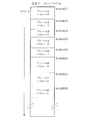
- FIG. 9 shows a configuration example of a communication system as a related technique using the selective repeat ARQ.
- the outline of transmission and reception in this communication system will be described as follows.
- a sequential sequence number SQN
- an ACK Acknowledgement
- an ACK frame is not returned.
- the data transmitting apparatus 90 when an ACK frame is returned within a certain time, it is considered that the frame with the sequence number has been transmitted correctly to the data receiving apparatus 910, while an ACK frame is not returned within the certain time. In this case, only the frame with the sequence number is retransmitted on the assumption that the frame with the sequence number did not reach the data receiving apparatus 910 correctly.
- frames 1 to 3 are normally received by the data receiving apparatus and an ACK frame is returned to the data transmitting apparatus, but frame 4 is lost on the transmission path, and the data receiving apparatus ACK frame is not returned to the data transmitting apparatus, timeout occurs, and frame 4 is retransmitted from the data transmitting apparatus.
- NACK Negative Acknowledgment
- the SQN adding circuit 91 adds a continuous transmission SQN value (transmission sequence number) for each frame, and transmits the frame data and the transmission SQN value to the transmission data buffer 92. To store. Next, in response to a read instruction from the transmission data buffer control circuit 93, the frame data and the transmission SQN value are read out. A frame generation circuit 94 that receives this adds a header and a trailer to generate a transmission frame and sends it to the downstream transmission line 100. An example of the trailer is a CRC (Cyclic Redundancy Check) value for frame error detection. Simultaneously with transmission of the transmission frame, the transmission SQN value is input to the retransmission timer 98, and counting of the retransmission timer corresponding to the transmission SQN value is started.
- CRC Cyclic Redundancy Check
- the frame inspection circuit 911 inspects the header and trailer. If the inspection result indicates that there is an abnormality in the transmission frame, the frame inspection circuit 911 discards the frame. If the inspection result indicates normal reception of the transmission frame, the frame is transferred to the SQN detection circuit 912.
- the SQN detection circuit 912 extracts the received SQN value and transfers it to the ACK generation circuit 915, while transferring it to the reception data buffer control circuit 913 and storing the reception payload data in the reception data buffer 914.
- the ACK generation circuit 916 that has received the received SQN value generates ACK frame payload data from the SQN value, and returns the ACK frame from the frame generation circuit 916 to the data transmission device 90 via the uplink transmission path 110.
- the frame inspection circuit 95 of the data transmission apparatus 90 When receiving a frame from the upstream transmission path 110, the frame inspection circuit 95 of the data transmission apparatus 90 performs a CRC inspection to confirm that there is no error in the frame. Then, the reception SQN value stored in the ACK frame is extracted by the ACK reception circuit 96 and transferred to the transmission data buffer control circuit 93 and the retransmission timer 98.
- the timer corresponding to the transmission SQN value of the retransmission timer 98 that starts counting simultaneously with the transmission of the transmission frame monitors whether or not the ACK frame is returned within a predetermined time, that is, whether or not a timeout has occurred. When a time-out occurs, the transmission data buffer control circuit 93 is notified of the time-out SQN value, and a retransmission is instructed.
- the transmission data buffer control circuit 93 reads the time-out SQN value and the corresponding payload data from the transmission data buffer 92 again, and retransmits them to the transmission line 100 via the frame generation circuit 94.
- the transmission data buffer control circuit 93 releases an area in which the payload data of the transmission data buffer 92 corresponding to the SQN value is stored, and transmits other frames. Make writable.
- the retransmission frame is received by the data reception device 910, if the retransmission frame is normally received, the received payload data is stored in the reception data buffer 914.
- the frame can be normally transmitted by retransmitting the frame by the Selective Repeat ARQ method.
- the frame 4 is discarded by the first transfer, the sequential frame transfer is performed as shown in FIGS. Is performed next, the storage order of the retransmitted frame 4 in the reception data buffer 914 is the arrival order of the frames as shown in FIG.
- Such storage in the reception data buffer 914 is because the frame length information cannot be obtained by discarding the frame 4, and the storage area to be secured between the frame 3 and the frame 5 in the reception process is unknown.
- the payload data of the frame to which the sequence number is assigned cannot be stored in the continuous memory area of the reception data buffer. In such a storage state, it is necessary to secure the frame order in communication, and therefore a read process of reading from the received data buffer in order of SQN values is necessary. Therefore, in order to process the frame sequence stored at non-consecutive addresses in order from the lowest number of SQN, it is necessary to manage the SQN value of the frame and the address where the frame is stored in association with each other.
- the data buffer frame write process and the read process are complicated, and an increase in the circuit scale of the control circuit is inevitable. Since writing and reading to such non-consecutive addresses must be performed, the processing speed is restricted, and as a result, it is difficult to increase the bandwidth.
- the present invention has been made in view of the above circumstances, and provides a data transmission method, a data transmission system, a data transmission device, a data reception device, and a control program capable of achieving simplification of data access processing and the like. It is an object.
- a first configuration of the present invention relates to a data transmission method, and a data transmission side uses data as a write address for storing data for each data transmission unit in a reception-side storage means.
- the data to which the write address is added is sequentially transmitted in the data transmission unit, and the data received on the data receiving side is sequentially specified by the write address added to the data.
- the data is stored in the storage position of the side storage means.
- a second configuration of the present invention relates to a data transmission system, wherein the data transmission unit sequentially transmits the data to which the write address for storing the data for each data transmission unit is stored in the receiving side storage means in the data transmission unit. And a data receiving device for storing the sequentially received data in a storage location of the receiving storage means specified by the write address added to the data.
- the write address or the write address head value on the data receiving side is generated on the data transmitting side and transmitted to the data receiving side, the access control processing on the data receiving side is simplified. Is obtained.
- the data transmission device includes an input unit that sequentially inputs data in units of data transmission, and an address generation unit that generates a write address for storing the data for each data transmission unit in a reception-side storage unit. Adding means for adding the generated write address to the data for each data transmission unit; and transmitting means for sequentially transmitting the data to which the write address has been added by the adding means in the data transmission unit. It becomes. Further, the data receiving device adds the data sequentially received by the receiving means, the receiving-side storage means, and the receiving means to the data transmitted from the transmitting means in the data transmission unit. Storage control means for storing in the storage position of the receiving-side storage means designated by the written address.
- Another embodiment of the data transmission apparatus includes an input unit that sequentially inputs data in variable-length data transmission units, a measurement unit that measures the data length of the data for each input data transmission unit, and the data Address generating means for calculating and generating the start value of the write address for storing the data for each transmission unit in the receiving side storage means based on the start value of the write address given to the immediately preceding data and the data length; Adding means for adding the start value of the write address calculated and generated by the address generation means to the data for each data transmission unit; and adding the data to which the start value of the write address is added by the addition means. Transmitting means for sequentially transmitting in units of data transmission.
- the receiving unit that receives the data transmitted from the transmitting unit in the unit of data transmission, the receiving-side storage unit, and the data sequentially received by the receiving unit, Storage control means for storing the data in the storage position of the reception-side storage means specified by the head value of the write address added to the data.
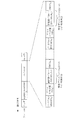
- FIG. 1 is a block diagram showing an electrical configuration of a communication system having a write address notification type retransmission control function according to Embodiment 1 of the present invention
- FIG. 2 is a transmission of the communication system having the same write address notification type retransmission control function
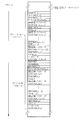
- FIG. 3 is a diagram illustrating a configuration example of a storage area of a data buffer
- FIG. 3 is a diagram illustrating a configuration example of a reception data buffer of a communication system having the same write address notification type retransmission control function
- FIG. It is a figure which shows the structural example of the frame format transmitted / received by the communication system which has a retransmission control function.
- the communication system 1 having a write address notification type retransmission control function relates to a system that can eliminate the complexity of write / read processing of a received data buffer before and after retransmission of data performed when an error occurs in received data.
- the data transmission device 10 and the data reception device 110 include a transmission path 30 from the data transmission device 10 to the data reception device 110, and a transmission path 130 from the data reception device 110 to the data transmission device 10. Connected with.
- the data transmitting apparatus 10 includes an SQN adding circuit 11, a frame length counting counter 12, a write address (WADR) calculating circuit 13, a transmission data buffer 14, a write address (WADR) adding circuit 15, and a transmission data buffer.
- the control circuit 16, the frame generation circuit 18, the frame inspection circuit 19, the ACK reception circuit 20, and the retransmission timer 21 are configured, while the data reception device 110 includes the frame inspection circuit 111 and the SQN detection.
- the SQN addition circuit 11 responds to the input K data (K is a positive integer of 1 or more) (data for each data transmission unit) for each frame (data transmission unit) in response to the input Kth variable length.
- K is a positive integer of 1 or more
- This is a circuit that adds a transmission sequence number incremented by 1 (SQN (K): K is a positive integer of 1 or more) to the data for frame K and supplies it to the transmission data buffer 14.
- the frame length counting counter 12 is a circuit that counts the payload data size L (K) (data length) of the frame K in response to the input frame K data and supplies it to the write address calculation circuit 13.
- This is a circuit that calculates and supplies the write address head value to the transmission data buffer 14.
- the write address calculation circuit 13 also performs control so that WADR (K) does not exceed the reception data buffer size Bmax.
- the transmission data buffer 14 stores the data for frame K, the SQN number, and the write address head value for each frame.
- the transmission data buffer 14 receives the frame K in response to a read instruction given from the transmission data buffer control circuit 16 via the read control line 17.
- WADR write address adding circuit 15.
- the storage mode of frames in the transmission data buffer 14 stores the SQN number of each frame, the write address head value WADR (K), and payload data in order from the lowest transmission SQN number. It is like going.
- SQN (1) is written at the head of the address.
- SQN (1) is not always stored at the head of the address.
- the write address (WADR) addition circuit 15 is a circuit that sets the transmission SQN (K) and WADR (K) received from the transmission data buffer 14 in the transmission SQN area and WADR area of each frame and transfers them to the transmission data buffer control circuit 16 It is.
- the transmission data buffer control circuit 16 transfers the frame received from the write address addition circuit 15 to the frame generation circuit 18, while the SQN received from the ACK reception circuit 20 when the timer corresponding to the reception SQN number of the retransmission timer 21 has not timed out.
- a read instruction is sent to the transmission data buffer 14 via the read control line 17. This is a control means for reading again the frame (SQN (K), WADR (K) and payload data) corresponding to the SQN number received from the ACK receiving circuit 20 from the transmission data buffer 14 and passing it to the frame generation circuit 18.
- the frame generation circuit 18 is a circuit that adds a header and a trailer to the frame from the transmission data buffer control circuit 16 and transmits the frame to the downstream transmission path 30 and transfers the transmission SQN number to the retransmission timer 21.
- the format of the variable length frame transferred via the downstream transfer path 30 is shown in FIG.
- the frame K includes a header area, a transmission SQN value (K), a write address head value WADR (K), payload data, and a trailer.
- the header portion may include the length information of the payload, and the length information of the payload may not be included in the frame header as in Ethernet (registered trademark) prescribed by the IEEE 802.3 committee. It may be a frame.
- An example of the trailer added by the frame generation circuit 18 is a CRC value for frame error.
- the retransmission timer 21 starts counting the timer corresponding to the transmission SQN number received from the frame generation circuit 18 and monitors whether the timer corresponding to the reception SQN number received from the ACK reception circuit 20 described later has timed out.
- Control circuit means for sending out the SQN number and the retransmission instruction to the transmission data buffer control circuit 16 when the ACK receiving circuit 20 does not receive the received SQN value and times out after a predetermined time elapses.
- the frame check circuit 19 performs CRC check on the ACK frame received via the uplink transmission path 130 to confirm the presence / absence of a frame error, transfers the ACK frame to the ACK reception circuit 20, and is received from the uplink transmission path 130.
- the Bmax notification frame is transferred to the write address calculation circuit 13.
- the ACK reception circuit 20 is a circuit that extracts the reception SQN number set in the ACK frame received from the frame check circuit 19 and transfers it to the transmission data buffer control circuit 16 and the retransmission timer 21.
- the frame inspection circuit 111 inspects the header and trailer (CRC value) of the frame received via the downlink transfer path 30 and transfers the frame to the SQN detection circuit 112 if it is normal reception. This circuit discards the frame if there is an abnormality.
- the SQN detection circuit 112 is a circuit that extracts the SQN number set in the received frame and transfers it to the ACK generation circuit 116 and transfers the frame to the write address (WADR) detection circuit 113.
- the write address detection circuit 113 is a circuit that extracts the write address head value (received WADR (K) value) of the received frame and transfers the write address head value and the frame to the received data buffer control circuit 114.
- the reception data buffer control circuit 114 is a circuit that controls writing of the received frame to the reception data buffer 115 based on the received write address head value.
- the reception data buffer 114 is a circuit unit that stores the payload data of the received frame based on the received write address head value, and sends the reception data buffer size Bmax to the reception data buffer size notification unit 117.
- the storage mode of the frames in the reception data buffer 115 is such that the payload data of each frame can be stored in order from the youngest reception SQN number.
- SQN 1 is written at the head of access.
- SQN (1) is not always stored at the head of the address.
- the ACK generation circuit 116 is a circuit that generates ACK frame payload data from the received SQN value received from the SQN detection circuit 112 and transfers this to the frame generation circuit 118.
- the reception data buffer size notification unit 117 is a notification unit that generates a notification frame of the reception data buffer size Bmax received from the reception data buffer 115 and transfers it to the frame generation circuit 118.
- the frame generation circuit 118 sends the ACK frame payload data received from the ACK generation circuit 116 to the upstream transfer path 130 as an ACK frame (also referred to as normal reception notification), and the reception data buffer size from the reception data buffer size notification means 117. This is a circuit for sending a Bmax notification frame to the upstream transfer path 130.
- the buffer size Bmax of the reception data buffer 115 is notified from the data reception device 110 to the data transmission device 10 prior to frame transmission / reception. .
- This notification is performed by sending a Bmax notification frame in which the Bmax value is stored in the payload to the write address calculation circuit 13 via the frame generation circuit 118, the upstream transmission path 130, and the frame inspection circuit 19.
- This notification may be performed only once if the buffer size of the reception data buffer 115 is not changed.
- the write address calculation circuit 13 calculates the write address start value WADR (K) to the reception data buffer 115 from WADR (K-1) and L (K-1) of the immediately preceding frame K-1 by the equation (1).
- the write address head value is transferred to the transmission data buffer 14.
- the write address calculation circuit 13 also performs control so that the calculated write address head value WADR (K) does not exceed the reception data buffer size Bmax.
- the transmission data buffer 14 stores the data for frame K, the SQN number, and the write address head value for each frame, while in response to a read instruction from the transmission data buffer control counter 12 via the read control line 17.
- the write address head value, transmission SQN number, and frame K data are read and supplied to the write address (WADR) adding circuit 15.
- WADR write address adding circuit 15.
- an example of a manner of storing frames in the transmission data buffer 11 is to store the SQN number, the write address head value WADR (K), and the payload data in order from the youngest transmission SQN number.
- FIG. 2 SQN (1) is written at the access head, but when the transmission data buffer 11 has a ring memory configuration, SQN (1) is not always stored at the address head.
- the write address addition circuit 15 sets the transmission SQN (K) and WADR (K) received from the transmission data buffer 14 in the transmission SQN area and WADR area of each frame and transfers them to the transmission data buffer control circuit 16.
- the transmission data buffer control circuit 16 transfers the frame received from the write address addition circuit 15 to the frame generation circuit 18.
- the frame generation circuit 18 adds a header and a trailer to the frame from the transmission data buffer control circuit 16 and transmits the frame to the downstream transmission path 30.
- An example of a trailer added by the frame generation circuit 18 is a CRC value for a frame error.
- the frame generation circuit 18 also transfers the transmission SQN number to the retransmission timer 21.
- the retransmission timer 21 starts counting the timer corresponding to the SQN number.
- the frame transmitted to the downlink transmission path 30 is received by the data reception device 110.
- the frame inspection circuit 111 inspects the header and trailer (CRC value) of the frame. If the frame is normally received, the frame inspection circuit 111 transfers the frame to the SQN detection circuit 112. If there is an error, the frame is discarded.
- the SQN detection circuit 112 extracts the SQN number (SQN (K)) set in the received frame, transfers it to the ACK generation circuit 116, and transfers the frame to the write address detection circuit 113.
- the write address detection circuit 113 extracts the write address start value (received WADR (K)) of the received frame and transfers the write address start value and the frame to the received data buffer control circuit 114.
- the reception data buffer control circuit 114 writes the received frame in the reception data buffer 115 based on the received write address head value.
- the reception SQN number (SQN (K)) is transferred from the SQN detection circuit 112 to the ACK generation circuit 116, and the ACK generated by the ACK generation circuit 116 is generated.
- the signal (ACK frame payload data) is transferred to a frame generation circuit 118 that generates an ACK frame.
- the frame generation circuit 118 returns the generated ACK frame to the data transmission device 10 via the uplink transfer path 130.
- the frame checking circuit 19 transfers the ACK frame to the ACK receiving circuit 20.
- the ACK reception circuit 20 obtains a reception SQN value from the ACK frame and sends it to the transmission data buffer control circuit 16 and the retransmission timer 21.
- the retransmission timer 21 determines (determines) that the timer corresponding to the reception SQN value has not timed out, and in this case, does not send a retransmission instruction to the transmission data buffer control circuit 16.
- the transmission data buffer control circuit 16 releases the payload data storage area corresponding to the reception SQN value received from the ACK reception circuit 20 and enables writing of another frame.
- the retransmission timer 19 of the data transmission apparatus 10 monitors whether the timer corresponding to the SQN value of the transmission frame has timed out, and the transmission frame is discarded by the data reception apparatus 110 and When the timer corresponding to the SQN value times out, the retransmission timer 19 sends a retransmission instruction corresponding to the time-out SQN value to the transmission data buffer control circuit 16.
- the transmission data buffer control circuit 16 Upon receiving this retransmission instruction, the transmission data buffer control circuit 16 sends a read instruction to the transmission data buffer 14 via the read control line 17, and SQN (K), WADR (corresponding to the SQN number received from the retransmission timer 19. K) and the payload data are read again from the transmission data buffer 14 and passed to the frame generation circuit 18.
- the frame K data, the SQN number, and the write address head value read from the transmission data buffer 14 are the frame K data, the SQN number, and the write address head value read when transmitting the discarded transmission frame. Is the same as the value.
- the storage location where the retransmitted frame is normally received by the data reception device 110 and written to the reception data buffer 115 will be written if it was written to the reception data buffer 115 without retransmission. It is the same as the memory location. That is, continuity of addresses is ensured. This also applies to reading from the reception data buffer 115.
- the storage location it is necessary to change the storage location depending on the presence / absence of retransmission, whether writing to or reading from the reception data buffer of the communication system having the write address notification type retransmission control function. Since it is possible to access the reception data buffer, it is possible to simplify the write or read processing in the reception data buffer, achieving a wider transmission band and especially a reduction in the circuit scale on the reception side. obtain.
- FIG. 5 is a block diagram showing an electrical configuration of a communication system having a write address notification type retransmission control function according to Embodiment 2 of the present invention
- FIG. 6 shows transmission / reception in the communication system having the same write address notification type retransmission control function
- FIG. 7 is a diagram showing a storage mode in a transmission data buffer of a communication system having the same write address notification type retransmission control function
- FIG. 8 is a diagram showing the same write address notification type retransmission control function. It is a figure which shows the storage aspect in the reception data buffer of the communication system which has.
- the configuration of this embodiment is greatly different from that of the first embodiment in that the frame payload is divided into a plurality of data blocks and retransmission control is performed for each data block. That is, the communication system 1A having the write address notification type retransmission control function of this embodiment has a data block dividing circuit 54 between the SQN addition circuit 11 of the data transmission device 50 and the transmission data buffer 55 as shown in FIG.
- ACK / NACK receiving circuit 61 is provided between frame check circuit 60 and transmission data buffer control circuit 57, while SQN detecting circuit 112 of data receiving device 510 and write address detecting circuit (WADR detecting circuit) 513 A data block inspection circuit 512 is provided between them, and an ACK / NACK generation circuit 516 is provided between the SQN detection circuit 112 and the data block inspection circuit 512 and the frame generation circuit 518, and the main part thereof is configured.
- K is a positive integer of 1 or more
- N fixed-length data blocks also referred to as fixed-length payload data
- DATA K, n K
- a data block number also referred to as a BNUM value
- O address offset value
- the ACK / NACK reception circuit 61 transmits the ACK type and reception SQN number (also referred to as reception SQN value) extracted from the ACK frame to the transmission data buffer control circuit 57 and the retransmission.
- the received frame is a NACK frame to the timer 62
- the NACK type extracted from the NACK frame, the received SQN value and the error data block number BNUM (n K ) (also referred to as the BNUM value) are transmitted data buffer control circuit 57 and a circuit for transferring to the retransmission timer 62.
- the data block inspection circuit 512 performs CRC inspection for each fixed-length payload, and when the data block is an error data block DATA (K, n K ), the error data block number BNUM (n K ) (both error BNM value) Is transferred to the ACK / NACK generation circuit 516, and when the data block is normal, the fixed-length data block DATA (K, n K ) is replaced with the write address head value (reception WADR (K) value) and the data block.
- This is a circuit that transfers to the write address detection circuit 513 together with a corresponding (BNUM (K) compatible) address offset O (n K ).
- the ACK / NACK generation circuit 516 is a circuit that generates ACK / NACK frame payload data for a received frame from the reception SQN number from the SQN detection circuit 111 and the error BNUM value from the data block check circuit 512. Specifically, the operation of the ACK / NACK generation circuit 516 generates an ACK signal when there is no error data block in the frame having the received SQN number, and transmits the ACK signal from the frame generation circuit 518 to the upstream transfer path 130 as an ACK frame.
- a NACK signal is generated and sent from the frame generation circuit 518 to the upstream transmission line 130 as a NACK frame (abnormal reception notification) of the error data block. .
- the transmission data buffer 55 includes fixed-length payload data from the data block dividing circuit 54, fixed-length payload data number (BNUM (n K )) and address offset value O (n K ), and a write address from the write address calculation circuit 53.
- the head value (WADR (K)) is stored so as to be readable in units of these information.
- the write address adding circuit 56 receives fixed length payload data, fixed length payload data number (BNUM (n K) read from the transmission data buffer 55 in response to a read instruction given from the transmission data buffer control circuit 57 via the read line 58. )),
- the address offset value O (n K ) and the write address head value (WADR (K)) are stored in the corresponding storage area of the frame to be transmitted and transferred to the transmission data buffer control circuit 57.
- the transmission data buffer control circuit 57 passes the frame from the write address addition circuit 56 to the frame generation circuit 18, and the release processing operation in response to the ACK type and reception SQN value from the ACK / NACK reception circuit 61 is the same.
- the data block retransmission processing operation in response to the retransmission instruction from the retransmission timer 62 and the NACK type, received SQN value, and BNUM value from the ACK / NACK receiving circuit 61 is different. That is, in the data block retransmission processing operation, the fixed length payload data corresponding to the BNUM value, the write address head value, and the address offset value in the frame specified by the received SQN value are to be retransmitted.
- the frame check circuit 60 has a difference in transferring an ACK frame or a NACK frame received via the uplink transmission path 130 to the ACK / NACK receiving circuit 45.
- the retransmission timer 62 is the same as transferring a retransmission instruction when an ACK frame is not received within a certain time to the transmission data buffer control circuit 57, but receives a NACK frame within a certain time or receives a NACK frame within a certain time. When the frame is not received, a retransmission instruction is transferred to the transmission data buffer control circuit 57.
- the write address detection circuit 513 generates a write address [WADR (K) + O (n K )] from the received WADR (K) value input from the data block inspection circuit 512 and the address offset value O (n K ).
- This is a circuit that transfers the received data buffer control circuit 514 together with the corresponding fixed-length data block DATA (K, n K ).
- the reception data buffer control circuit 514 stores the fixed-length data block DATA (K, n K ) input from the write address detection circuit 513 in the write address [WADR (K) + O (n K )] of the reception data buffer 115. Circuit.
- the frame generation circuit 518 is a circuit that transmits the ACK frame or NACK frame from the ACK / NACK generation circuit 516 and the Bmax notification frame from the reception data buffer size notification unit 117 to the uplink transmission path 130. Since the constituent elements of this embodiment other than this constituent element are the same as those of the first embodiment, the same reference numerals are given to the same constituent portions, and the description thereof will be omitted.
- the data reception device 510 prior to frame transmission / reception, notifies the data transmission device 50 of the buffer size Bmax of the reception data buffer 115.
- this notification is performed by sending a Bmax notification frame in which the Bmax value of the buffer size is stored in the payload to the write address calculation circuit 13 via the frame generation circuit 518, the upstream transmission path 130, and the frame inspection circuit 60. This notification need only be made once if the size of the reception data buffer 115 is not changed.
- the write address calculation circuit 13 calculates the write address head value WADR (K) to the reception data buffer 115 from the WADR (K-1) and L (K-1) of the immediately preceding frame K-1 by the equation (1).
- the write address head value is transferred to the transmission data buffer 55.
- the write address calculation circuit 13 also performs control so that the calculated write address head value WADR (K) does not exceed the Bmax value of the reception data buffer size notified by the Bmax notification frame supplied from the frame inspection circuit 60. Do.
- the data block dividing circuit 54 converts the input data for frame K into N fixed-length data blocks (fixed-length payload data) (also referred to as data blocks) DATA (K, n K ).
- the data is divided, a data block number BNUM (n K ) and an address offset value O (n K ) are generated for each of the divided fixed-length data blocks DATA (K, n K ), and the divided fixed-length data blocks DATA ( K, n K ), data block number BNUM (n K ), and address offset value O (n K ) are transferred to the transmission data buffer 55.
- the transmission data buffer 55 stores the SQN (K), WADR (K), data block, and BNUM (n K ) and O (n K ) for each data block for each frame in a readable manner. (See FIG. 6)
- the content of the read instruction given from the transmission data buffer control circuit 57 via the read control line 58 that is, the entire frame at the time of frame transmission or the data block at the time of retransmission of the data block DATA (K, n K ), WADR (K), and O (n K ) are read and supplied to the write address (WADR) adding circuit 56.
- WADR write address
- the SQN value (SQN (K)), the write address head value WADR (K), The block number BNUM (n K ), the address offset value O (n K ), and fixed-length payload data DATA (K, n K ) are stored.
- the write address (WADR) addition circuit 56 transmits the transmission SQN value received from the transmission data buffer 11 to each of the transmission SQN area, WADR area, BNUM area, and address offset area of each frame, WADR (K), BNUM (n K ), and O (n K ) is set and transferred to the transmission data buffer control circuit 57.
- the transmission data buffer control circuit 57 transfers the frame received from the write address addition circuit 56 to the frame generation circuit 18.
- the frame generation circuit 18 adds a header and a trailer to the frame from the transmission data buffer control circuit 57 and transmits the frame to the transmission path 30, and transfers the transmission SQN value to the retransmission timer 62.
- An example of a trailer added by the frame generation circuit 18 is a CRC value for a frame error.
- the retransmission timer 62 starts counting the retransmission timer of the transmission SQN value received from the frame generation circuit 18 and starts monitoring whether the timer corresponding to the reception SQN value received from the ACK / NACK generation circuit 61 has timed out. .
- the SQN detection circuit 112 receives a frame via the downlink transmission path 30, the SQN value set in the frame is extracted and transferred to the ACK / NACK generation circuit 516 and the frame is transferred to the data block check circuit 512. To do.
- the data block inspection circuit 512 performs a CRC inspection for each data block of the frame.
- the write address detection circuit 513 uses the write address start value (received WADR (K)) and the address offset value as the write address for the data block. since the O (n K), the as write address of the data block to generate a WADR (K) + O (n K), the data block passes the data block and the write address to the receive data buffer controller 514 The data is stored in the write address of the reception data buffer 115.
- the ACK / NACK control circuit 516 generates an ACK signal from the received SQN value from the SQN detection circuit 112 and inputs the ACK signal to the frame generation circuit 518 as an ACK frame via the uplink transmission path 130. Send to.
- the frame check circuit 60 of the data transmitting apparatus 50 transfers the ACK frame to the ACK / NACK receiving circuit 61, and transfers the ACK type and the received SQN value to the transmission data buffer control circuit 57 and the retransmission timer 62.
- the retransmission timer 62 does not output a retransmission instruction because the ACK type and the received SQN value are received within a certain time.
- the transmission data buffer control circuit 57 releases the payload storage area corresponding to the received SQN value to prepare for writing another frame.
- the data block check circuit 512 discards the data block and ACK / NACK BNUM (n K ). Transfer to the generation circuit 516.
- the ACK / NACK check circuit 516 generates a NACK signal from the received SQN value input from the SQN detection circuit 112 and the BNUM value input from the data block check circuit 512, and transmits the NACK frame from the frame generation circuit 518 to the upstream transmission line 130. Send to.
- the CRC check is performed to confirm that there is no frame error, and the frame is transferred to the ACK / NACK reception circuit 61.
- the ACK / NACK receiving circuit 61 extracts the NACK type, the received SQN value, and the BNUM value from the frame, and transfers them to the transmission data buffer control circuit 57 and the retransmission timer 62.
- the retransmission timer 62 sends a retransmission instruction to the transmission data buffer control circuit 57 in response to receiving the NACK type, the received SQN value, and the BNUM value within a predetermined time.
- the retransmission timer 62 sends a retransmission instruction to the transmission data buffer control circuit 57 in response to not receiving the NACK type, the received SQN value, and the BNUM value within a predetermined time.
- the transmission data buffer control circuit 57 uses the NACK type from the ACK / NACK reception circuit 61, the reception SQN value and the reception BNUM value, and the retransmission instruction from the retransmission timer 62, and the head of the write address for the frame determined by the reception SQN value.
- An instruction to read the value (WADR (K)), the data block data corresponding to the received BNUM value, and the address offset value is sent to the transmission data buffer 55 via the read line 58.
- Each piece of information read from the transmission data buffer 55 is framed by the frame generation circuit 18 and transmitted to the downstream transmission path 30.
- the transmission data buffer control circuit 57 does not receive the NACK type, the reception SQN value, and the BNUM value within a predetermined time, and when a retransmission instruction is transmitted from the retransmission timer 62, the transmission data buffer control circuit 57 determines the frame determined by the SQN value corresponding to timeout. Perform retransmission control.
- the data block check circuit 512 that has received the frame transmitted via the downlink transmission path 30 via the SQN detection circuit 112 of the data reception device 510 detects the write address when there is no error in the retransmitted data block of the frame. Transfer to circuit 513.
- the write address detection circuit 513 performs the write address head value (reception WADR (K)) and the address offset value O (n K ) as the write address for the data block in the same manner as described above for the case of normal reception of the data block. ), WADR (K) + O (n K ) is generated as the write address of the data block, the data block and the write address are passed to the reception data buffer control circuit 514, and the data block is received by the reception data buffer 115. Is stored at the above write address. Further, the ACK / NACK control circuit 516 returns an ACK frame for the data block data DATA (K, n K ), which is an error data block, to the data reception device 50 via the frame generation circuit 518.
- the ACK / NACK receiving circuit 61 of the data transmitting apparatus 50 When the ACK / NACK receiving circuit 61 of the data transmitting apparatus 50 receives the ACK frame, the data block area notified by the ACK frame is released, and the corresponding data block of another frame can be written. If there is no error data block other than the ACK frame for the data block data DATA (K, n K ) that was the error data block, the frame area corresponding to the SQN value of the frame is released, and another frame Allows writing of payload data.
- the write address of the data block is determined for each data block, even if the data block is received in error and the data block is discarded, the data block received in the error data block is normally received.
- the write addresses in the address space (FIG. 8) of the reception data buffer 115 are consecutive addresses in the order of the sequence numbers. Therefore, processing on the reading side of the reception data buffer 115 is facilitated, and downsizing and widening of the bandwidth can be enjoyed.
- the write address head value WADR (K) + O (n K ) in each frame is the write address of the reception data buffer 115 as it is. However, if the relative relationship of each frame does not change, WADR (K) Alternatively, an address obtained by uniformly adding an offset value may be used.
- the same effect as that of the first embodiment can be obtained in the division of the payload of the frame to the receiving side of the communication system having the write address notification type retransmission control function.
- the effect is obtained in units of data blocks.
- the write address may be generated by providing means other than measurement of the payload data size of the frame, for example, means for holding the size of fixed-length payload data. Further, the generation mode of the write address may not be based on the write address head value.
- the present invention can be applied to various communication systems that transmit and receive data in units of data transmission.
Landscapes
- Engineering & Computer Science (AREA)
- Computer Networks & Wireless Communication (AREA)
- Signal Processing (AREA)
- Communication Control (AREA)
- Detection And Prevention Of Errors In Transmission (AREA)
- Data Exchanges In Wide-Area Networks (AREA)
Abstract
Description
この発明は、データ伝送方法、データ伝送システム、データ送信装置、データ受信装置、及び制御プログラムに係り、詳しくは、データの受信の際のアドレス制御処理の複雑化の回避に有用なデータ伝送方法、データ伝送システム、データ送信装置、データ受信装置、及び制御プログラムに関する。 The present invention relates to a data transmission method, a data transmission system, a data transmission device, a data reception device, and a control program. More specifically, the present invention relates to a data transmission method useful for avoiding complication of address control processing when receiving data, The present invention relates to a data transmission system, a data transmission device, a data reception device, and a control program.
データ通信を首尾良く行うための手段として、フレーム再送制御方式が、従来から知られている。このフレーム再送制御方式は、データ送信装置とデータ受信装置との間でフレーム通信を行う際にデータ受信装置で受信するフレームにエラーが生じたとしても、フレームを正しく受信するための誤り制御方式である。
この再送制御方式の1つにSelective Repeat ARQ(Automatic Repeat request)方式がある。
As a means for successfully performing data communication, a frame retransmission control method has been conventionally known. This frame retransmission control method is an error control method for correctly receiving a frame even if an error occurs in a frame received by the data receiving device when performing frame communication between the data transmitting device and the data receiving device. is there.
One of the retransmission control methods is a Selective Repeat ARQ (Automatic Repeat request) method.
このSelective Repeat ARQを用いた、関連技術としての通信システムの構成例を図9に示す。
この通信システムでの送受信の大要を説明すると、次のようになる。データ送信装置90が順次に発出するフレームに、連続するシーケンス番号(SQN)を付加し、そのフレームをデータ受信装置910で正しく受信できた場合には、該シーケンス番号のACK(Acknowledgement)フレームを返送するが、フレームの欠落やビットエラーにより受信できなかった場合にはACKフレームを返送しない。
データ送信装置90において、一定時間内にACKフレームが返送される場合には該シーケンス番号のフレームはデータ受信装置910に正しく伝送できたものと見做す一方、一定時間内にACKフレームが返送されない場合には該シーケンス番号のフレームはデータ受信装置910に正しく届かなかったものとして該シーケンス番号のフレームのみを再送する。
FIG. 9 shows a configuration example of a communication system as a related technique using the selective repeat ARQ.
The outline of transmission and reception in this communication system will be described as follows. When a sequential sequence number (SQN) is added to the frames that are sequentially transmitted by the data transmitting apparatus 90 and the data receiving apparatus 910 can correctly receive the frames, an ACK (Acknowledgement) frame of the sequence number is returned. However, if reception is not possible due to frame loss or bit error, an ACK frame is not returned.
In the data transmitting apparatus 90, when an ACK frame is returned within a certain time, it is considered that the frame with the sequence number has been transmitted correctly to the data receiving apparatus 910, while an ACK frame is not returned within the certain time. In this case, only the frame with the sequence number is retransmitted on the assumption that the frame with the sequence number did not reach the data receiving apparatus 910 correctly.
例えば、図10に示すように、フレーム1からフレーム3までは、データ受信装置で正常に受信されてデータ送信装置へACKフレームが返送されたが、フレーム4が伝送路上で欠落し、データ受信装置からデータ送信装置へACKフレームが返送されず、タイムアウトが生じ、データ送信装置からフレーム4が再送される。
このように、正しく受信できなかったフレームのみを再送することにより、効率的な伝送路の利用を行うことができる。
なお、フレームの受信が正しく行われなかったとき、データ送信装置に対してNACK(Negative Acknowledgment)フレームを返送する方式もある。
For example, as shown in FIG. 10,
In this way, by efficiently retransmitting only frames that could not be received correctly, it is possible to efficiently use the transmission path.
There is also a method of returning a NACK (Negative Acknowledgment) frame to the data transmitting apparatus when the frame is not correctly received.
上述のフレーム再送についての具体例を図9を参照して説明する。
データ送信装置90にフレーム用データが入力されると、先ず、SQN付加回路91でフレーム毎に連続する送信SQN値(送信シーケンス番号)を付加してフレーム用データと送信SQN値を送信データバッファ92に格納する。
次に、送信データバッファ制御回路93からの読み出し指示により、フレーム用データと送信SQN値を読み出す。これを受け取るフレーム生成回路94でヘッダとトレイラを付加して送信フレームを生成して下り伝送路100へ送出する。トレイラの例としては、フレーム誤り検出用のCRC(Cyclic Redundancy Check)値である。
送信フレームの伝送と同時に、送信SQN値を再送タイマ98に入力し、当該送信SQN値対応の再送タイマのカウントを開始する。
A specific example of the above-described frame retransmission will be described with reference to FIG.
When frame data is input to the data transmitter 90, first, the
Next, in response to a read instruction from the transmission data
Simultaneously with transmission of the transmission frame, the transmission SQN value is input to the
一方、データ受信装置910では、送信フレームが入力されると、フレーム検査回路911でヘッダとトレイラの検査を行う。検査結果が送信フレームに異常があることを示している場合には、そのフレームをフレーム検査回路911で破棄する。
検査結果が、送信フレームの正常受信を示しているならば、そのフレームはSQN検出回路912に転送する。SQN検出回路912は、受信SQN値を取り出してACK生成回路915へ転送する一方、受信データバッファ制御回路913に転送して受信ペイロードデータを受信データバッファ914に格納する。
受信SQN値を受け取ったACK生成回路916は、そのSQN値からACKフレーム用ペイロードデータを生成し、フレーム生成回路916からACKフレームを上り伝送路110を介してデータ送信装置90へ返送する。
On the other hand, in the data receiving device 910, when a transmission frame is input, the
If the inspection result indicates normal reception of the transmission frame, the frame is transferred to the
The
データ送信装置90のフレーム検査回路95は、上り伝送路110からフレームを受信すると、CRC検査を行い、フレームに誤りが無いことを確認する。
そして、ACK受信回路96でACKフレームに格納されている受信SQN値を取り出し、送信データバッファ制御回路93と再送タイマ98に転送する。
送信フレームの送信と同時にカウントを開始した再送タイマ98の送信SQN値対応のタイマが一定時間以内にACKフレームが返送されるか否か、すなわち、タイムアウトしていないか否かを監視しており、タイムアウトしたときにはタイムアウトしたSQN値を送信データバッファ制御回路93に通知して再送を指示する。
When receiving a frame from the
Then, the reception SQN value stored in the ACK frame is extracted by the
The timer corresponding to the transmission SQN value of the
送信データバッファ制御回路93は、再度送信データバッファ92からタイムアウトしたSQN値とこれに該当するペイロードデータを読み出し、フレーム生成回路94経由で、伝送路100に再送する。
なお、送信データバッファ制御回路93は、ACK受信回路96から受信SQN値が入力されると、該SQN値に該当する送信データバッファ92のペイロードデータが格納されている領域を開放し、他のフレームを書き込み可能にする。
上記の再送フレームが、データ受信装置910で受信されると、その再送フレームが正常受信したならば、その受信ペイロードデータを受信データバッファ914に格納する。
The transmission data
When the reception SQN value is input from the
When the retransmission frame is received by the data reception device 910, if the retransmission frame is normally received, the received payload data is stored in the
上述した関連技術としての通信システムでも、受信したフレームにエラー等の障害が発生すると、そのフレームをSelective Repeat ARQ方式で再送することにより、フレームの正常な伝送を行うことはできる。
しかしながら、例えば、図10に示すように、フレーム送信中にそのフレーム4が1回目の転送で破棄され、順次のフレーム転送が図10及び図11のように行われてフレーム4の再送がフレーム7の次に行われると、再送されたフレーム4の受信データバッファ914への格納順序は、図12に示すように、フレームの到着順となる。
Even in the communication system as the related technology described above, when a failure such as an error occurs in the received frame, the frame can be normally transmitted by retransmitting the frame by the Selective Repeat ARQ method.
However, for example, as shown in FIG. 10, during transmission of the frame, the
このような受信データバッファ914への格納は、フレーム4の破棄により、そのフレーム長情報を入手できず、受信処理においてフレーム3とフレーム5との間に確保すべき格納領域が不明のために、シーケンス番号を付与されているフレームのペイロードデータが、受信データバッファの連続したメモリ領域に格納することができなくなる。このような格納状態になると、通信におけるフレーム順序の確保をしなければならないことから、受信データバッファよりSQN値順に読み出すリード処理が必要である。
そのため、非連続なアドレスに格納されたフレーム列をSQNの若番より順序良く処理するために、フレームのSQN値と、該フレームが格納されたアドレスとを対応付けて管理する必要があり、受信データバッファのフレームのライト処理も、また、リード処理も複雑になり、その制御回路の回路規模の増大が避けられない。
このような非連続なアドレスへのライト、そしてリードを行なわなくてはならないから、それらの処理速度の制約となり、結果として広帯域化が難しくなる。
Such storage in the
Therefore, in order to process the frame sequence stored at non-consecutive addresses in order from the lowest number of SQN, it is necessary to manage the SQN value of the frame and the address where the frame is stored in association with each other. The data buffer frame write process and the read process are complicated, and an increase in the circuit scale of the control circuit is inevitable.
Since writing and reading to such non-consecutive addresses must be performed, the processing speed is restricted, and as a result, it is difficult to increase the bandwidth.
この発明は、上述の事情に鑑みてなされたもので、データのアクセス処理の簡略化等を達成し得るデータ伝送方法、データ伝送システム、データ送信装置、データ受信装置、及び制御プログラムを提供することを目的としている。 The present invention has been made in view of the above circumstances, and provides a data transmission method, a data transmission system, a data transmission device, a data reception device, and a control program capable of achieving simplification of data access processing and the like. It is an object.
上記課題を解決するために、この発明の第1の構成は、データ伝送方法に係り、データ送信側にて、データ伝送単位毎のデータを受信側記憶手段に記憶させるための書き込みアドレスをデータに付加し、前記書き込みアドレスが付加された前記データを前記データ伝送単位で順次伝送し、データ受信側にて、順次受信した前記データを、当該データに付加された前記書き込みアドレスで指定される前記受信側記憶手段の記憶位置に記憶することを特徴としている。 In order to solve the above-described problems, a first configuration of the present invention relates to a data transmission method, and a data transmission side uses data as a write address for storing data for each data transmission unit in a reception-side storage means. In addition, the data to which the write address is added is sequentially transmitted in the data transmission unit, and the data received on the data receiving side is sequentially specified by the write address added to the data. The data is stored in the storage position of the side storage means.
この発明の第2の構成は、データ伝送システムに係り、データ伝送単位毎のデータを受信側記憶手段に記憶させるための書き込みアドレスが付加された前記データを前記データ伝送単位で順次伝送するデータ送信装置と、順次受信した前記データを、当該データに付加された前記書き込みアドレスで指定される前記受信側記憶手段の記憶位置に記憶するデータ受信装置とからなることを特徴としている。 A second configuration of the present invention relates to a data transmission system, wherein the data transmission unit sequentially transmits the data to which the write address for storing the data for each data transmission unit is stored in the receiving side storage means in the data transmission unit. And a data receiving device for storing the sequentially received data in a storage location of the receiving storage means specified by the write address added to the data.
この発明の構成によれば、データ受信側の書き込みアドレス乃至書き込みアドレス先頭値をデータ送信側で生成してデータ受信側へ伝送するようにしているので、データ受信側のアクセス制御処理の簡略化等が得られる。 According to the configuration of the present invention, since the write address or the write address head value on the data receiving side is generated on the data transmitting side and transmitted to the data receiving side, the access control processing on the data receiving side is simplified. Is obtained.
1、1A 通信システム(データ伝送システム)
11 SQN付加回路(入力手段)
12 フレーム長計数カウンタ(アドレス生成手段、計測手段)
13 ライトアドレス算出回路(アドレス生成手段)
14、55 送信データバッファ(アドレス生成手段)
15、56 ライトアドレス付加回路(付加手段)
16、57 送信データバッファ制御回路(送信手段)
18 フレーム生成回路
19、60 フレーム検出回路
20 ACK受信回路
21、62 再送タイマ(判別手段)
54 データブロック分割回路(アドレス生成手段、分割手段)
61 ACK/NACK受信回路
111 フレーム検査回路(受信手段)
112 SQN検出回路(判別手段)
113、513 ライトアドレス検出回路(記憶制御手段)
114、514 受信データバッファ制御回路
115 受信データバッファ(記憶手段)
116 ACK生成回路
118、518 フレーム生成回路
512 データブロック検査回路
516 ACK/NACK受信回路
1, 1A communication system (data transmission system)
11 SQN addition circuit (input means)
12 Frame length counter (address generating means, measuring means)
13 Write address calculation circuit (address generation means)
14, 55 Transmission data buffer (address generation means)
15, 56 Write address addition circuit (addition means)
16, 57 Transmission data buffer control circuit (transmission means)
18
54 Data block dividing circuit (address generating means, dividing means)
61 ACK /
112 SQN detection circuit (discriminating means)
113, 513 Write address detection circuit (storage control means)
114, 514 Reception data
116
この発明の最良の形態は、データ受信側で必要な書き込みアドレスをデータ送信側で生成すること及びその書き込みアドレスの受信側への伝送を含んで実現される。
具体的には、データ送信装置は、データ伝送単位でデータを順次入力する入力手段と、前記データ伝送単位毎の前記データを受信側記憶手段に記憶させるための書き込みアドレスを生成するアドレス生成手段と、生成された前記書き込みアドレスを前記データ伝送単位毎の前記データに付加する付加手段と、該付加手段によって前記書き込みアドレスが付加された前記データを前記データ伝送単位で順次伝送する送信手段とを備えてなる。また、データ受信装置は、前記送信手段から伝送される前記データを前記データ伝送単位で受信する受信手段と、前記受信側記憶手段と、前記受信手段によって順次受信した前記データを、当該データに付加された前記書き込みアドレスで指定される前記受信側記憶手段の記憶位置に記憶させる記憶制御手段とを備えてなる。
The best mode of the present invention is realized by generating a write address required on the data receiving side on the data transmitting side and transmitting the write address to the receiving side.
Specifically, the data transmission device includes an input unit that sequentially inputs data in units of data transmission, and an address generation unit that generates a write address for storing the data for each data transmission unit in a reception-side storage unit. Adding means for adding the generated write address to the data for each data transmission unit; and transmitting means for sequentially transmitting the data to which the write address has been added by the adding means in the data transmission unit. It becomes. Further, the data receiving device adds the data sequentially received by the receiving means, the receiving-side storage means, and the receiving means to the data transmitted from the transmitting means in the data transmission unit. Storage control means for storing in the storage position of the receiving-side storage means designated by the written address.
また、別の形態のデータ送信装置は、可変長のデータ伝送単位でデータを順次入力する入力手段と、入力される前記データ伝送単位毎の前記データのデータ長を計測する計測手段と、前記データ伝送単位毎の前記データを受信側記憶手段に記憶させるための書き込みアドレスの先頭値を、直前データに与えられた前記書き込みアドレスの先頭値と前記データ長とに基づいて算出生成するアドレス生成手段と、該アドレス生成手段によって算出生成された前記書き込みアドレスの先頭値を前記データ伝送単位毎の前記データに付加する付加手段と、該付加手段によって前記書き込みアドレスの先頭値が付加された前記データを前記データ伝送単位で順次伝送する送信手段とを備えてなる。また、別の形態のデータ受信装置は、前記送信手段から伝送される前記データを前記データ伝送単位で受信する受信手段と、前記受信側記憶手段と、前記受信手段によって順次受信した前記データを、当該データに付加された前記書き込みアドレスの先頭値で指定される前記受信側記憶手段の記憶位置に記憶させる記憶制御手段とを備えてなる。 Another embodiment of the data transmission apparatus includes an input unit that sequentially inputs data in variable-length data transmission units, a measurement unit that measures the data length of the data for each input data transmission unit, and the data Address generating means for calculating and generating the start value of the write address for storing the data for each transmission unit in the receiving side storage means based on the start value of the write address given to the immediately preceding data and the data length; Adding means for adding the start value of the write address calculated and generated by the address generation means to the data for each data transmission unit; and adding the data to which the start value of the write address is added by the addition means. Transmitting means for sequentially transmitting in units of data transmission. In another form of the data receiving apparatus, the receiving unit that receives the data transmitted from the transmitting unit in the unit of data transmission, the receiving-side storage unit, and the data sequentially received by the receiving unit, Storage control means for storing the data in the storage position of the reception-side storage means specified by the head value of the write address added to the data.
図1は、この発明の実施形態1であるライトアドレス通知型再送制御機能を有する通信システムの電気的構成を示すブロック図、図2は、同ライトアドレス通知型再送制御機能を有する通信システムの送信データバッファの格納領域の構成例を示す図、図3は、同ライトアドレス通知型再送制御機能を有する通信システムの受信データバッファの構成例を示す図、また、図4は、同ライトアドレス通知型再送制御機能を有する通信システムで送受信されるフレームフォーマットの構成例を示す図である。
この実施形態のライトアドレス通知型再送制御機能を有する通信システム1は、受信データのエラー時に行われるデータの再送の前後における受信データバッファのライト・リード処理の複雑化を除き得るシステムに係り、図1に示すように、そのデータ送信装置10とデータ受信装置110とは、データ送信装置10からデータ受信装置110への伝送路30と、データ受信装置110からデータ送信装置10への伝送路130とで接続されている。
1 is a block diagram showing an electrical configuration of a communication system having a write address notification type retransmission control function according to
The
そして、データ送信装置10は、SQN付加回路11と、フレーム長計数カウンタ12と、ライトアドレス(WADR)算出回路13と、送信データバッファ14と、ライトアドレス(WADR)付加回路15と、送信データバッファ制御回路16と、フレーム生成回路18と、フレーム検査回路19と、ACK受信回路20と、再送タイマ21とを有して構成される一方、データ受信装置110は、フレーム検査回路111と、SQN検出回路112と、ライトアドレス(WADR)検出回路113と、受信データバッファ制御回路114と、受信データバッファ115と、ACK生成回路116と、受信データバッファサイズ通知手段117と、フレーム生成回路118とを有して構成されている。
Then, the data transmitting apparatus 10 includes an
先ず、上述したデータ送信装置10の各構成要素の各各について説明する。
SQN付加回路11は、入力されるK番目の可変長であるフレームK用データ(Kは1以上の正の整数)(データ伝送単位毎のデータ)に応答してフレーム(データ伝送単位)毎に1ずつインクリメントした送信シーケンス番号(SQN(K):Kは1以上の正の整数)をフレームK用データに付加して送信データバッファ14へ供給する回路である。
First, each of each component of the data transmission apparatus 10 mentioned above is demonstrated.
The
フレーム長計数カウンタ12は、入力されるフレームK用データに応答してそのフレームKのペイロードデータサイズL(K)(データ長)を計数してライトアドレス算出回路13に供給する回路であり、ライトアドレス算出回路13は、受信データバッファ115への該フレームKの書き込みアドレスの先頭値(以下、ライトアドレス先頭値という)WADR(K)を次式
WADR(K)=WADR(K-1)+L(K-1) ……(1)
但し、WADR(K-1)は直前のフレームK-1のライトアドレス先頭値、L(K-1)はフレームK-1のペイロードデータサイズである。
により算出してそのライトアドレス先頭値を送信データバッファ14へ供給する回路である。また、ライトアドレス算出回路13は、WADR(K)が受信データバッファサイズBmaxを超過しないようにする制御も行う。
The frame
However, WADR (K-1) is the write address head value of the immediately preceding frame K-1, and L (K-1) is the payload data size of the frame K-1.
This is a circuit that calculates and supplies the write address head value to the
送信データバッファ14は、フレーム毎に、フレームK用データとSQN番号とライトアドレス先頭値とを格納する一方、送信データバッファ制御回路16から読み出し制御線17を介して与えられる読み出し指示により、フレームK用データ、SQN番号及びライトアドレス先頭値を読み出してライトアドレス(WADR)付加回路15に供給する記憶手段である。
送信データバッファ14へのフレームの格納態様は、図2に示すように、送信SQN番号の若番より順番に、各フレームのSQN番号、ライトアドレス先頭値WADR(K)、そしてペイロードデータを格納して行く如きものである。図2では、アドレス先頭にSQN(1)を記してあるが、送信データバッファ14をリングメモリ構成としている場合には、必ずしもアドレス先頭にSQN(1)が格納されているとは限らない。
The
As shown in FIG. 2, the storage mode of frames in the
ライトアドレス(WADR)付加回路15は、各フレームの送信SQN領域とWADR領域に送信データバッファ14から受け取る送信SQN(K)とWADR(K)を設定して送信データバッファ制御回路16へ転送する回路である。
送信データバッファ制御回路16は、ライトアドレス付加回路15から受け取るフレームをフレーム生成回路18へ転送する一方、再送タイマ21の受信SQN番号対応のタイマがタイムアウトしていないとき、ACK受信回路20から受け取るSQN番号に対応するペイロードデータ格納領域の開放を行って他のフレームの書き込みを可能にするほか、再送タイマ21から再送指示を受け取るときには読み出し制御線17を介して送信データバッファ14に読み出し指示を送出してACK受信回路20から受け取るSQN番号に該当するフレーム(SQN(K)、WADR(K)及びペイロードデータ)を送信データバッファ14から再度読み出してフレーム生成回路18へ渡す制御手段である。
The write address (WADR)
The transmission data
フレーム生成回路18は、送信データバッファ制御回路16からのフレームにさらにヘッダとトレイラとを付加して下り伝送路30へ送信すると共に、送信SQN番号を再送タイマ21へ転送する回路である。
下り転送路30を経て転送される可変長フレームのフォーマットを図4に示す。フレームKは、ヘッダ領域、送信SQN値(K)、ライトアドレス先頭値WADR(K)、ペイロードデータ、トレイラで構成される。このうち、ヘッダ部には、ペイロードのLength情報を含んでいても良く、また、IEEE802.3委員会が規定するイーサネット(登録商標)のように、フレームヘッダ中にペイロードのLength情報を含くまないフレームであっても良い。また、フレーム生成回路18で付加されるトレイラの例としては、フレーム誤り用のCRC値である。
The
The format of the variable length frame transferred via the
再送タイマ21は、フレーム生成回路18から受け取る送信SQN番号対応のタイマの計時を開始すると共に後述するACK受信回路20から受け取る受信SQN番号対応のタイマがタイムアウトしていないか否かを監視しており、ACK受信回路20から受信SQN値の入力がなく所定時間経過してタイムアウトする時に当該SQN番号及び再送指示を送信データバッファ制御回路16へ送出する制御回路手段である。
The
フレーム検査回路19は、上り伝送路130を介して受信するACKフレームのCRC検査を行ってフレーム誤りの存否を確認してACKフレームをACK受信回路20へ転送すると共に、上り伝送路130から受信されるBmax通知フレームをライトアドレス算出回路13へ転送する回路である。
ACK受信回路20は、フレーム検査回路19から受け取るACKフレームに設定されている受信SQN番号を取り出して送信データバッファ制御回路16及び再送タイマ21へ転送する回路である。
The
The
次に、上述したデータ受信装置110の各構成要素の各各について説明する。
フレーム検査回路111は、下り転送路30を介して受信されるフレームのヘッダとトレイラ(CRC値)の検査を行って、正常受信ならばそのフレームをSQN検出回路112へ転送するが、受信フレームに異常があるならばそのフレームを破棄する回路である。
SQN検出回路112は、受け取るフレームに設定されているSQN番号を取り出してACK生成回路116へ転送すると共に、そのフレームをライトアドレス(WADR)検出回路113へ転送する回路である。ライトアドレス検出回路113は、受け取るフレームのライトアドレス先頭値(受信WADR(K)値)を取り出してそのライトアドレス先頭値とフレームとを受信データバッファ制御回路114へ転送する回路である。
Next, each component of the
The
The
受信データバッファ制御回路114は、受け取ったライトアドレス先頭値に基づく受け取ったフレームの受信データバッファ115への書き込み制御を行う回路である。受信データバッファ114は、受け取ったライトアドレス先頭値に基づいて受け取ったフレームのペイロードデータを格納するほか、受信データバッファサイズBmaxを受信データバッファサイズ通知手段117へ送出する回路手段である。
受信データバッファ115へのフレームの格納態様は、図3に示すように、受信SQN番号の若番より順番に、各フレームのペイロードデータを格納し得る如きものである。図3では、アクセス先頭にSQN=1を記してあるが、受信データバッファ115をリングメモリ構成としている場合には、必ずしもアドレス先頭にSQN(1)が格納されているとは限らない。
The reception data
As shown in FIG. 3, the storage mode of the frames in the
ACK生成回路116は、SQN検出回路112から受け取る受信SQN値からACKフレーム用ペイロードデータを生成し、これをフレーム生成回路118へ転送する回路である。受信データバッファサイズ通知手段117は、受信データバッファ115から受け取った受信データバッファサイズBmaxの通知フレームを生成してフレーム生成回路118へ転送する通知手段である。
フレーム生成回路118は、ACK生成回路116から受け取るACKフレーム用ペイロードデータをACKフレーム(正常受信通知ともいう)として上り転送路130へ送出するほか、受信データバッファサイズ通知手段117からの受信データバッファサイズBmax通知フレームを上り転送路130へ送出する回路である。
The
The
次に、図1乃至図4を参照して、この実施形態の動作を説明する。
この実施形態のライトアドレス通知型再送制御機能を有する通信システム1において、フレームの送受信を行うのに先立って、データ受信装置110からデータ送信装置10へ、受信データバッファ115のバッファサイズBmaxを通知する。この通知は、ペイロードにBmax値を格納したBmax通知フレームをフレーム生成回路118、上り伝送路130、フレーム検査回路19経由でライトアドレス算出回路13に送り込んで行う。この通知は、受信データバッファ115のバッファサイズに変更がなければ、一度のみでよい。
Next, the operation of this embodiment will be described with reference to FIGS.
In the
まず、上記バッファサイズBmaxが通知された後のデータ送信装置10の動作から説明する。
フレームK用データ(Kは1以上の正の整数)がSQN付加回路11に入力されると、SQN付加回路11は、フレーム毎に1ずつインクリメントした送信シーケンス番号(SQN(K):Kは1以上の正の整数)をフレームK用データに付加して送信データバッファ14へ転送する。
また、各フレーム用データは、フレーム長計数カウンタ12に入力される。フレーム長計数カウンタ12は、入力されたフレーム用データに応答してそのフレームKのペイロードデータサイズL(K)を計数してライトアドレス算出回路13に供給する。
First, the operation of the data transmitting apparatus 10 after the notification of the buffer size Bmax will be described.
When frame K data (K is a positive integer of 1 or more) is input to the
Each frame data is input to the
ライトアドレス算出回路13は、受信データバッファ115へのライトアドレス先頭値WADR(K)を式(1)により直前のフレームK-1のWADR(K-1)及びL(K-1)から算出してそのライトアドレス先頭値を送信データバッファ14へ転送する。また、ライトアドレス算出回路13は、算出されるライトアドレス先頭値WADR(K)が受信データバッファサイズBmaxを超過しないようにする制御も行う。
The write
送信データバッファ14は、フレーム毎に、フレームK用データと、SQN番号と、ライトアドレス先頭値とを格納する一方、読み出し制御線17を介しての送信データバッファ制御カウンタ12からの読み出し指示により、ライトアドレス先頭値と、送信SQN番号と、フレームK用データとを読み出してライトアドレス(WADR)付加回路15に供給する。
送信データバッファ11へのフレームの格納態様の例は、上述したように、送信SQN番号の若番より順番に、SQN番号、ライトアドレス先頭値WADR(K)、そしてペイロードデータを格納する如きものであるが(図2)、これに限らない。例えば、図2では、アクセス先頭にSQN(1)を記してあるが、送信データバッファ11をリングメモリ構成としている場合には、必ずしもアドレス先頭にSQN(1)が格納されるとは限らない。
The
As described above, an example of a manner of storing frames in the
ライトアドレス付加回路15は、各フレームの送信SQN領域とWADR領域に送信データバッファ14から受け取る送信SQN(K)とWADR(K)を設定して送信データバッファ制御回路16へ転送する。
送信データバッファ制御回路16は、ライトアドレス付加回路15から受け取るフレームをフレーム生成回路18へ転送する。
フレーム生成回路18は、送信データバッファ制御回路16からのフレームにさらにヘッダとトレイラとを付加して下り伝送路30へ送信する。フレーム生成回路18で付加されるトレイラの例は、フレーム誤り用のCRC値である。
フレーム生成回路18は、また、送信SQN番号を再送タイマ21へ転送する。再送タイマ21は、そのSQN番号対応のタイマの計時を開始する。
The write
The transmission data
The
The
上述のようにして、下り伝送路30に送信されたフレームは、データ受信装置110で受信される。
そのフレームをフレーム検査回路111が受信すると、フレーム検査回路111は、フレームのヘッダとトレイラ(CRC値)の検査を行って、正常受信ならばそのフレームをSQN検出回路112へ転送するが、受信フレームに異常があるならばそのフレームを破棄する。
As described above, the frame transmitted to the
When the
SQN検出回路112は、受け取るフレームに設定されているSQN番号(SQN(K))を取り出してACK生成回路116へ転送すると共に、そのフレームをライトアドレス検出回路113へ転送する。
ライトアドレス検出回路113は、受け取るフレームのライトアドレス先頭値(受信WADR(K)を取り出してそのライトアドレス先頭値とフレームとを受信データバッファ制御回路114へ転送する。
受信データバッファ制御回路114は、受け取ったライトアドレス先頭値に基づいて受け取ったフレームを受信データバッファ115に書き込む。
The
The write address detection circuit 113 extracts the write address start value (received WADR (K)) of the received frame and transfers the write address start value and the frame to the received data
The reception data
上述のように、データ受信装置110でフレームを正常に受信すると、受信SQN番号(SQN(K))が、SQN検出回路112からACK生成回路116へ転送され、ACK生成回路116で生成されたACK信号(ACKフレーム用ペイロードデータ)がACKフレームを生成するフレーム生成回路118へ転送される。
フレーム生成回路118は、生成したACKフレームを上り転送路130を介してデータ送信装置10へ返送する。
As described above, when the
The
そのACKフレームを受け取るデータ送信装置10では、そのフレーム検査回路19は、ACKフレームをACK受信回路20へ転送する。ACK受信回路20は、ACKフレームから受信SQN値を得て、これを送信データバッファ制御回路16及び再送タイマ21へ送る。
再送タイマ21は、受信SQN値対応のタイマがタイムアウトしていないことを判定(判別)し、その場合には、再送指示を送信データバッファ制御回路16に送出しない。
これに応答して、送信データバッファ制御回路16は、ACK受信回路20から受け取る受信SQN値に対応するペイロードデータ格納領域の開放を行って他のフレームの書き込みを可能にする。
In the data transmitting apparatus 10 that receives the ACK frame, the
The
In response to this, the transmission data
また、上述のように、データ受信装置110で受信するフレームが異常であることが検出されてそのフレームが破棄され、SQN検出回路112から受信SQN値がACK生成回路116へ送られず、この場合にはデータ受信装置110からデータ送信装置10へACKフレームが返されない。
一方、データ送信装置10の再送タイマ19では、送信フレームのSQN値対応のタイマが、タイムアウトしているか否かを監視しており、その送信フレームがデータ受信装置110で破棄されて上記送信フレームのSQN値対応のタイマが、タイムアウトするときには、再送タイマ19からタイムアウトしたSQN値対応の再送指示が送信データバッファ制御回路16へ送られる。
Further, as described above, it is detected that the frame received by the
On the other hand, the
この再送指示を受けた送信データバッファ制御回路16は、読み出し制御線17を介して送信データバッファ14に読み出し指示を送出して再送タイマ19から受け取ったSQN番号に対応するSQN(K)、WADR(K)及びペイロードデータを送信データバッファ14から再度読み出してフレーム生成回路18へ渡す。
このとき送信データバッファ14から読み出されるフレームK用データと、SQN番号と、ライトアドレス先頭値は、破棄された送信フレームの送信時に読み出されたフレームK用データと、SQN番号と、ライトアドレス先頭値と同一である。
したがって、その再送されたフレームが、データ受信装置110で、正常に、受信され、受信データバッファ115に書き込まれる記憶場所は、再送なしに受信データバッファ115に書き込まれたなら、書き込まれるであろう記憶場所と同一となる。つまり、アドレスの連続性が担保される。このことは、受信データバッファ115からのリードでも同じである。
Upon receiving this retransmission instruction, the transmission data
At this time, the frame K data, the SQN number, and the write address head value read from the
Therefore, the storage location where the retransmitted frame is normally received by the
このように、この実施形態によれば、ライトアドレス通知型再送制御機能を有する通信システムの受信データバッファへのライトでも、また、そこからのリードでも、再送の有無によって記憶場所の変更を要することなく、受信データバッファへのアクセスを可能にしたから、受信データバッファでのライト又はリード処理を簡略化することが可能になり、伝送の広帯域化や、特に受信側の回路規模の削減を達成し得る。 As described above, according to this embodiment, it is necessary to change the storage location depending on the presence / absence of retransmission, whether writing to or reading from the reception data buffer of the communication system having the write address notification type retransmission control function. Since it is possible to access the reception data buffer, it is possible to simplify the write or read processing in the reception data buffer, achieving a wider transmission band and especially a reduction in the circuit scale on the reception side. obtain.
図5は、この発明の実施形態2であるライトアドレス通知型再送制御機能を有する通信システムの電気的構成を示すブロック図、図6は、同ライトアドレス通知型再送制御機能を有する通信システムで送受されるフレームフォーマットを示す図、図7は、同ライトアドレス通知型再送制御機能を有する通信システムの送信データバッファ内の格納態様を示す図、また、図8は、同ライトアドレス通知型再送制御機能を有する通信システムの受信データバッファ内の格納態様を示す図である。
FIG. 5 is a block diagram showing an electrical configuration of a communication system having a write address notification type retransmission control function according to
この実施形態の構成が、実施形態1のそれと大きく異なる点は、フレームのペイロードを複数のデータブロックに分け、データブロック毎の再送制御を行うようにした点である。
すなわち、この実施形態のライトアドレス通知型再送制御機能を有する通信システム1Aは、図5に示すように、データ送信装置50のSQN付加回路11と送信データバッファ55との間にデータブロック分割回路54を設け、フレーム検査回路60と送信データバッファ制御回路57との間にACK/NACK受信回路61を設ける一方、データ受信装置510のSQN検出回路112とライトアドレス検出回路(WADR検出回路)513との間にデータブロック検査回路512を設け、SQN検出回路112及びデータブロック検査回路512とフレーム生成回路518との間にACK/NACK生成回路516を設けて、その主要部が構成されている。
The configuration of this embodiment is greatly different from that of the first embodiment in that the frame payload is divided into a plurality of data blocks and retransmission control is performed for each data block.
That is, the
データブロック分割回路54は、入力されるフレームK用データ(Kは1以上の正の整数)を、図6に示すように、N個の固定長データブロック(固定長ペイロードデータともいう)DATA(K,nK)(n=1,2,…,Nのうちの1つ)に分割し、分割された固定長ペイロードデータ毎に、データブロック番号(BNUM値ともいう)(BNUM(nK))、及びアドレスオフセット値O(nK)を生成して送信データバッファ55に転送する回路である。
As shown in FIG. 6, the data block dividing
ACK/NACK受信回路61は、フレーム検査回路60から受け取るフレームがACKフレームであるときは、ACKフレームから取り出されるACK種別及び受信SQN番号(受信SQN値ともいう)を送信データバッファ制御回路57及び再送タイマ62へ、また、受け取るフレームがNACKフレームであるときは、NACKフレームから取り出されるNACK種別、並びに受信SQN値及びエラーデータブロック番号BNUM(nK)(BNUM値ともいう)を送信データバッファ制御回路57及び再送タイマ62へ転送する回路である。
When the frame received from the
データブロック検査回路512は、固定長ペイロード毎にCRC検査を行い、そのデータブロックがエラーデータブロックDATA(K,nK)であるとき、そのエラーデータブロック番号BNUM(nK)(エラーBNM値ともいう)をACK/NACK生成回路516へ転送する一方、データブロックが正常であるとき固定長データブロックDATA(K,nK)を、ライトアドレス先頭値(受信WADR(K)値)及び当該データブロック対応(BNUM(K)対応)のアドレスオフセットO(nK)と共にライトアドレス検出回路513に転送する回路である。
The data block
ACK/NACK生成回路516は、SQN検出回路111からの受信SQN番号及びデータブロック検査回路512からのエラーBNUM値から受信フレームに対するACK/NACKフレーム用ペイロードデータを生成する回路である。
ACK/NACK生成回路516の動作を具体的に言えば、上記受信SQN番号のフレームにエラーデータブロックが無かった場合にはACK信号を生成し、フレーム生成回路518からACKフレームとして上り転送路130へ送出する一方、エラーデータブロックDATA(K,nK)があった場合にはNACK信号を生成し、フレーム生成回路518からエラーデータブロックのNACKフレーム(異常受信通知)として上り伝送路130へ送出する。
The ACK /
Specifically, the operation of the ACK /
また、この実施形態のデータ送信装置50の構成要素のうちの次の構成要素に実施形態1と若干異なる点を有する。
送信データバッファ55は、データブロック分割回路54からの固定長ペイロードデータ、固定長ペイロードデータ番号(BNUM(nK))及びアドレスオフセット値O(nK)と、ライトアドレス算出回路53からのライトアドレス先頭値(WADR(K))とをこれらの情報の単位で読み出し可能に格納する。
ライトアドレス付加回路56は、送信データバッファ制御回路57から読み出し線58を介して与えられる読み出し指示に応答して送信データバッファ55から読み出される固定長ペイロードデータ、固定長ペイロードデータ番号(BNUM(nK))、アドレスオフセット値O(nK)及びライトアドレス先頭値(WADR(K))を送信しようとするフレームの対応する格納領域に格納して送信データバッファ制御回路57へ転送する。
Further, the following constituent elements of the constituent elements of the data transmission device 50 according to this embodiment are slightly different from the first embodiment.
The
The write
送信データバッファ制御回路57は、ライトアドレス付加回路56からのフレームをフレーム生成回路18へ渡すこと及びACK/NACK受信回路61からのACK種別及び受信SQN値に応答しての開放処理動作は同じであるが、再送タイマ62からの再送指示とACK/NACK受信回路61からのNACK種別、受信SQN値及びBNUM値とを受けてのデータブロック再送処理動作は異なる。すなわち、データブロック再送処理動作は、受信SQN値で指定されるフレームのうちのBNUM値対応の固定長ペイロードデータ、ライトアドレス先頭値及びアドレスオフセット値が再送されるべき対象とされる。
The transmission data
フレーム検査回路60は、上り伝送路130を経て受信されるACKフレーム 又はNACKフレームをACK/NACK受信回路45へ転送することに差異がある。
再送タイマ62は、一定時間内にACKフレームを受信しないときの再送指示を送信データバッファ制御回路57へ転送することは同じであるが、一定時間内にNACKフレームを受信する又は一定時間内にNACKフレームを受信しないときは、送信データバッファ制御回路57へ再送指示を転送する。
The
The
また、この実施形態のデータ受信装置510の構成要素のうちの次の構成要素に実施形態1と若干異なる点を有する。
ライトアドレス検出回路513は、データブロック検査回路512から入力される受信WADR(K)値とアドレスオフセット値O(nK)とからライトアドレス[WADR(K)+O(nK)]を生成して対応する固定長データブロックDATA(K,nK)と共に受信データバッファ制御回路514に転送する回路である。
受信データバッファ制御回路514は、ライトアドレス検出回路513から入力される固定長データブロックDATA(K,nK)を受信データバッファ115のライトアドレス[WADR(K)+O(nK)]に格納させる回路である。
フレーム生成回路518は、ACK/NACK生成回路516からのACKフレーム又はNACKフレーム及び受信データバッファサイズ通知手段117からのBmax通知フレームを上り伝送路130へ送出する回路である。
この構成要素以外の、この実施形態の構成要素は、実施形態1と同じであるので、同一構成部分には同一の参照番号を付して、その逐一の説明は省略する。
Further, the following constituent elements of the constituent elements of the data receiving apparatus 510 of this embodiment are slightly different from those of the first embodiment.
The write
The reception data
The
Since the constituent elements of this embodiment other than this constituent element are the same as those of the first embodiment, the same reference numerals are given to the same constituent portions, and the description thereof will be omitted.
次に、図4乃至図7を参照して、この実施形態の動作について説明する。
この実施形態の受信システム1Aにおいて、フレームの送受信を行うのに先立って、データ受信装置510からデータ送信装置50へ、受信データバッファ115のバッファサイズBmaxを通知する。この通知は、実施形態1と同様、ペイロードにバッファサイズのBmax値を格納したBmax通知フレームをフレーム生成回路518、上り伝送路130、フレーム検査回路60経由でライトアドレス算出回路13に送り込んで行う。この通知は、受信データバッファ115のサイズに変更がなければ、一度行うだけでよい。
Next, the operation of this embodiment will be described with reference to FIGS.
In the
上記バッファサイズのBmax値が通知された状態において、先ず、通信システム1Aの送信側の動作について説明する。
フレームK用データ(Kは1以上の正の整数)がSQN付加回路11に入力されると、SQN付加回路11は、フレーム毎に1ずつインクリメントした送信シーケンス番号(SQN(K):Kは1以上の正の整数)をフレームK用データに付加してデータブロック分割回路54へ供給する。
また、各フレーム用データは、フレーム長計数カウンタ12に入力される。フレーム長計数カウンタ12は、入力されたフレーム用データに応答してそのフレームKのペイロードデータサイズL(K)を計数してライトアドレス算出回路13に供給する。
First, the operation on the transmission side of the
When frame K data (K is a positive integer of 1 or more) is input to the
Each frame data is input to the
ライトアドレス算出回路13は、受信データバッファ115へのライトアドレス先頭値WADR(K)を式(1)により直前のフレームK-1のWADR(K-1)及びL(K-1)から算出してそのライトアドレス先頭値を送信データバッファ55へ転送する。ライトアドレス算出回路13は、算出されるライトアドレス先頭値WADR(K)が、フレーム検査回路60から供給されるBmax通知フレームで通知される受信データバッファサイズのBmax値を超過しないようにする制御も行う。
The write
データブロック分割回路54は、入力されるフレームK用データを、図6に示すように、N個の固定長データブロック(固定長ペイロードデータ)(データブロックともいう)DATA(K,nK)に分割し、分割された固定長データブロックDATA(K,nK)毎の、データブロック番号BNUM(nK)及びアドレスオフセット値O(nK)を生成し、分割された固定長データブロックDATA(K,nK)、データブロック番号BNUM(nK)及びアドレスオフセット値O(nK)を送信データバッファ55に転送する。
As shown in FIG. 6, the data block dividing
送信データバッファ55は、フレーム毎に、SQN(K)、WADR(K)、データブロック、データブロック毎のBNUM(nK)及びO(nK)をこれらの情報の単位で読み出し可能に格納する(図6参照)一方、送信データバッファ制御回路57から読み出し制御線58を介して与えられる読み出し指示の内容、すなわち、フレーム送信のときはフレーム全体を、又はデータブロックの再送のときは当該データブロックDATA(K,nK)、WADR(K)及びO(nK)を読み出してライトアドレス(WADR)付加回路56に供給する。
送信データバッファ55へのフレームの格納態様の例は、図7に示すように、送信SQN番号の若番より順番に、SQN値(SQN(K))、ライトアドレス先頭値WADR(K)、データブロック番号BNUM(nK)、アドレスオフセット値O(nK)、そして固定長ペイロードデータDATA(K,nK)を格納する如きものである。
The
As shown in FIG. 7, an example of a mode of storing frames in the
ライトアドレス(WADR)付加回路56は、各フレームの送信SQN領域、WADR領域、BNUM領域及びアドレスオフセット領域のそれぞれに送信データバッファ11から受け取る送信SQN値、WADR(K)、BNUM(nK)及びO(nK)を設定して送信データバッファ制御回路57へ転送する。
送信データバッファ制御回路57は、ライトアドレス付加回路56から受け取るフレームをフレーム生成回路18へ転送する。
The write address (WADR)
The transmission data
フレーム生成回路18は、送信データバッファ制御回路57からのフレームにさらにヘッダとトレイラとを付加して伝送路30へ送信すると共に、送信SQN値を再送タイマ62へ転送する。フレーム生成回路18で付加されるトレイラの例は、フレーム誤り用のCRC値である。
再送タイマ62は、フレーム生成回路18から受け取る送信SQN値の再送タイマのカウントを開始すると共に、ACK/NACK生成回路61から受け取る受信SQN値対応のタイマがタイムアウトしていないか否かの監視に入る。
The
The
次に、通信システム1Aの受信側の動作について説明する。
下り伝送路30を介してSQN検出回路112がフレームを受け取ると、そのフレームに設定されているSQN値を取り出してACK/NACK生成回路516へ転送すると共に、そのフレームをデータブロック検査回路512へ転送する。
Next, the operation on the receiving side of the
When the
データブロック検査回路512は、フレームのデータブロック毎にCRC検査を行う。データブロックについての検査結果が正常データブロックであることを示す場合には、ライトアドレス検出回路513が、そのデータブロックについてのライトアドレスとして、ライトアドレス先頭値(受信WADR(K))とアドレスオフセット値O(nK)とから、そのデータブロックのライトアドレスとしてWADR(K)+O(nK)を生成し、当該データブロックとそのライトアドレスとを受信データバッファ制御回路514へ渡して当該データブロックを受信データバッファ115の上記ライトアドレスに格納する。
また、ACK/NACK制御回路516は、SQN検出回路112からの受信SQN値からACK信号を生成し、これをフレーム生成回路518へ入力してACKフレームとして上り伝送路130を介してデータ送信装置50へ送信する。
The data block
Further, the ACK /
そのデータ送信装置50のフレーム検査回路60がACKフレームをACK/NACK受信回路61へ転送し、ACK種別と受信SQN値を送信データバッファ制御回路57及び再送タイマ62へ転送する。再送タイマ62は、ACK種別と受信SQN値が一定時間内に受信するので、再送指示を出力しない。
ACK種別と受信SQN値を受け取った送信データバッファ制御回路57は、受信SQN値対応のペイロードの格納領域の開放を行って他のフレームの書き込みに備える。
The
Receiving the ACK type and the received SQN value, the transmission data
データブロックについての検査結果が、エラーデータブロックDATA(K,nK)であることを示す場合には、データブロック検査回路512は、そのデータブロックを破棄し、BNUM(nK)をACK/NACK生成回路516へ転送する。ACK/NACK検査回路516は、SQN検出回路112から入力される受信SQN値とデータブロック検査回路512から入力されるBNUM値からNACK信号を生成し、フレーム生成回路518からNACKフレームを上り伝送路130に送信する。
If the check result for the data block indicates that it is an error data block DATA (K, n K ), the data
データ送信装置50のフレーム検査回路60でNACKフレームを受信すると、CRC検査を行い、フレーム誤りが無いことを確認し、そのフレームをACK/NACK受信回路61へ転送する。ACK/NACK受信回路61は、そのフレームからNACK種別、受信SQN値及びBNUM値を取り出し、送信データバッファ制御回路57及び再送タイマ62へ転送する。
再送タイマ62は、NACK種別、受信SQN値及びBNUM値を一定時間内に受信することに応答して再送指示を送信データバッファ制御回路57へ送出する。また、再送タイマ62は、一定時間内にNACK種別、受信SQN値及びBNUM値を受信しないことに応答して再送指示を送信データバッファ制御回路57へ送出する。
When the
The
送信データバッファ制御回路57は、ACK/NACK受信回路61からのNACK種別、受信SQN値及び受信BNUM値と再送タイマ62からの再送指示とに基づいて、受信SQN値で決まるフレームについてのライトアドレス先頭値(WADR(K))と、受信BNUM値対応のデータブロックデータ及びアドレスオフセット値の読み出し指示を読み出し線58を介して送信データバッファ55へ送る。送信データバッファ55から読み出された各情報はフレーム生成回路18でフレーム化されて下り伝送路30へ送信される。
また、送信データバッファ制御回路57は、一定時間内にNACK種別、受信SQN値及びBNUM値を受信せず、再送タイマ62から再送指示が送出されるときは、タイムアウト対応のSQN値で決まるフレームの再送制御を行う。
The transmission data
Also, the transmission data
下り伝送路30を経て伝送されて来たフレームをデータ受信装置510のSQN検出回路112を経て受信したデータブロック検査回路512は、フレームの再送データブロックにエラーがないとき、そのフレームをライトアドレス検出回路513に転送する。
ライトアドレス検出回路513は、データブロックの正常受信の場合について上述したと同様にして、そのデータブロックについてのライトアドレスとして、ライトアドレス先頭値(受信WADR(K))とアドレスオフセット値O(nK)とから、そのデータブロックのライトアドレスとしてWADR(K)+O(nK)を生成し、当該データブロックとそのライトアドレスとを受信データバッファ制御回路514へ渡して当該データブロックを受信データバッファ115の上記ライトアドレスに格納する。
また、ACK/NACK制御回路516からは、エラーデータブロックであったデータブロックデータDATA(K,nK)に対するACKフレームをフレーム生成回路518を介してデータ受信装置50へ返送する。
The data block
The write
Further, the ACK /
データ送信装置50のACK/NACK受信回路61が、そのACKフレームを受信すると、当該ACKフレームで通知されたデータブロック領域の開放を行い、他のフレームの対応データブロックの書き込みを可能にする。
なお、エラーデータブロックであったデータブロックデータDATA(K,nK)に対するACKフレーム以外にエラーデータブロックがない場合には、当該フレームのSQN値に対応するフレーム領域の開放を行い、他のフレームのペイロードデータの書き込みを可能にする。
When the ACK /
If there is no error data block other than the ACK frame for the data block data DATA (K, n K ) that was the error data block, the frame area corresponding to the SQN value of the frame is released, and another frame Allows writing of payload data.
上述のように、データブロック別に当該データブロックのライトアドレスが定まるから、たとえデータブロックがエラーで受信されて当該データブロックが破棄されたとしても、エラーデータブロックで受信されたデータブロックが正常に受信される場合のライトアドレスは、受信データバッファ115のアドレス空間(図8)では、シーケンス番号順に連続したアドレスとなる。
したがって、受信データバッファ115の読み出し側の処理が容易になり、小型化、広帯域化を享受し得る。
なお、図8では、各フレーム内のライトアドレス先頭値WADR(K)+O(nK)がそのまま受信データバッファ115のライトアドレスであるが、各フレームの相対関係が変わらなければ、WADR(K)に一律にオフセット値を加算したアドレスとしてもよい。
As described above, since the write address of the data block is determined for each data block, even if the data block is received in error and the data block is discarded, the data block received in the error data block is normally received. In this case, the write addresses in the address space (FIG. 8) of the
Therefore, processing on the reading side of the
In FIG. 8, the write address head value WADR (K) + O (n K ) in each frame is the write address of the
このように、この実施形態によれば、ライトアドレス通知型再送制御機能を有する通信システムの受信側へのフレームのペイロードの分割においても、実施形態1と同効を得ることができる。その効果は、データブロック単位で得られる。 As described above, according to this embodiment, the same effect as that of the first embodiment can be obtained in the division of the payload of the frame to the receiving side of the communication system having the write address notification type retransmission control function. The effect is obtained in units of data blocks.
以上、この発明の実施形態を、図面を参照して詳述してきたが、この発明の具体的な構成は、これらの実施形態に限られるものではなく、この発明の要旨を逸脱しない範囲の設計の変更等があってもそれらはこの発明に含まれる。
例えば、実施形態は、フレームの送信又は受信の制御をハードウェア構成で行う例について説明したが、それらの制御をソフトウェア制御で代替して構成することもできる。
また、フレームの正常受信のときに、受信データバッファへの書き込みを行うようにしているが、受信の正常又は異常を問わず、書き込みを行い、再送されて正常に受信されるフレームを上書きするようにしてもよい。
また、アドレスオフセット値を各データブロックに付加する例について説明したが、データブロック長が共通である場合には、必ずしもデータブロック毎に付加しなくてもよい。
また、書き込みアドレスは、フレームのペイロードデータサイズの計測以外の手段、例えば、固定長ペイロードデータであるときはそのサイズを保持する手段を設けて生成するように構成してもよい。また、書き込みアドレスの生成態様は、書き込みアドレス先頭値を基準にしなくてもよい。
Although the embodiments of the present invention have been described in detail with reference to the drawings, the specific configuration of the present invention is not limited to these embodiments, and the design does not depart from the gist of the present invention. These changes are included in the present invention.
For example, in the embodiment, an example in which frame transmission or reception control is performed using a hardware configuration has been described. However, such control may be configured by software control.
In addition, when the frame is normally received, writing to the reception data buffer is performed. However, regardless of whether the reception is normal or abnormal, the writing is performed, and the frame that is retransmitted and normally received is overwritten. It may be.
Further, although an example in which the address offset value is added to each data block has been described, when the data block length is common, it is not always necessary to add it to each data block.
The write address may be generated by providing means other than measurement of the payload data size of the frame, for example, means for holding the size of fixed-length payload data. Further, the generation mode of the write address may not be based on the write address head value.
この発明は、データ伝送単位でデータを送受信する各種の通信システムに適用できる。 The present invention can be applied to various communication systems that transmit and receive data in units of data transmission.
Claims (20)
データ受信側にて、順次受信した前記データを、当該データに付加された前記書き込みアドレスで指定される前記受信側記憶手段の記憶位置に記憶することを特徴とするデータ伝送方法。 On the data transmission side, a write address for storing data for each data transmission unit in the storage unit on the reception side is added to the data, and the data to which the write address is added is sequentially transmitted in the data transmission unit,
A data transmission method characterized in that the data received on the data receiving side is stored in the storage location of the receiving side storage means specified by the write address added to the data.
データ伝送単位でデータを順次入力し、
前記データ伝送単位毎の前記データを受信側記憶手段に記憶させるための書き込みアドレスを生成し、
生成された前記書き込みアドレスを前記データ伝送単位毎の前記データに付加し、
前記書き込みアドレスが付加された前記データを前記データ伝送単位で順次伝送し、
データ受信側にて、
前記データ送信装置から伝送される前記データを順次受信し、受信した当該データに付加された前記書き込みアドレスで指定される前記受信側記憶手段の記憶位置に記憶することを特徴とするデータ伝送方法。 On the data transmission side
Enter data sequentially in units of data transmission,
Generating a write address for storing the data for each data transmission unit in the receiving storage means;
Adding the generated write address to the data for each data transmission unit;
Sequentially transmitting the data with the write address added in the data transmission unit;
On the data receiving side,
A data transmission method comprising: sequentially receiving the data transmitted from the data transmission device and storing the data in a storage location of the receiving storage means specified by the write address added to the received data.
データ送信装置に可変長のデータ伝送単位でデータを順次入力し、
入力される前記データ伝送単位毎の前記データのデータ長を計測して保持し、
前記データ伝送単位毎の前記データを受信側記憶手段に記憶させるための書き込みアドレスの先頭値を、直前データに与えられた前記書き込みアドレスの先頭値と前記データ長とに基づいて算出生成し、
算出された前記書き込みアドレスの先頭値を前記データ伝送単位毎の前記データに付加し、
前記書き込みアドレスの先頭値が付加された前記データを前記データ伝送単位で順次伝送し、
データ受信側にて、
前記データ送信側から伝送される前記データを順次受信し、受信した当該データに付加された前記書き込みアドレスの先頭値で指定される前記受信側記憶手段の記憶位置に記憶することを特徴とするデータ伝送方法。 On the data transmission side
Data is sequentially input to the data transmission device in variable-length data transmission units,
Measure and hold the data length of the data for each input data transmission unit,
The head value of the write address for storing the data for each data transmission unit in the receiving side storage means is calculated and generated based on the head value of the write address given to the immediately preceding data and the data length,
Adding the calculated first value of the write address to the data for each data transmission unit;
The data to which the head value of the write address is added is sequentially transmitted in the data transmission unit,
On the data receiving side,
Data that sequentially receives the data transmitted from the data transmission side, and stores the data in a storage location of the reception side storage means specified by a head value of the write address added to the received data Transmission method.
前記データ受信側では、前記データブロックを前記書き込みアドレスの先頭値及び前記オフセット値に基づいて前記受信側記憶手段の記憶位置に記憶することを特徴とする請求項3記載のデータ伝送方法。 On the data transmission side, the data for each data transmission unit is divided into a predetermined number of data blocks, the head value of the write address is added to the data for each data transmission unit, and the data block for each data block A number and an offset value from the start value of the write address, and sequentially transmit the data to which the start value of the write address, the data block number and the offset value are added, in the data transmission unit,
4. The data transmission method according to claim 3, wherein the data receiving side stores the data block in a storage position of the receiving side storage means based on a head value of the write address and the offset value.
順次受信した前記データを、当該データに付加された前記書き込みアドレスで指定される前記受信側記憶手段の記憶位置に記憶するデータ受信装置とからなることを特徴とするデータ伝送システム。 A data transmission device for sequentially transmitting the data in units of the data transmission, to which the write address for storing the data for each data transmission unit in the reception-side storage unit is added;
A data transmission system comprising: a data receiving apparatus for storing the data received sequentially in a storage position of the receiving storage means designated by the write address added to the data.
前記データ伝送単位毎の前記データを受信側記憶手段に記憶させるための書き込みアドレスを生成するアドレス生成手段と、
生成された前記書き込みアドレスを前記データ伝送単位毎の前記データに付加する付加手段と、
該付加手段によって前記書き込みアドレスが付加された前記データを前記データ伝送単位で順次伝送する送信手段とを備えてなるデータ送信装置と、
該データ送信装置の前記送信手段から伝送される前記データを前記データ伝送単位で受信する受信手段と、
前記受信側記憶手段と、
前記受信手段によって順次受信した前記データを、当該データに付加された前記書き込みアドレスで指定される前記受信側記憶手段の記憶位置に記憶させる記憶制御手段とを備えてなるデータ受信装置とからなることを特徴とするデータ伝送システム。 Input means for sequentially inputting data in units of data transmission;
Address generating means for generating a write address for storing the data for each data transmission unit in the receiving storage means;
An adding means for adding the generated write address to the data for each data transmission unit;
A data transmission device comprising: transmission means for sequentially transmitting the data, to which the write address is added by the addition means, in the data transmission unit;
Receiving means for receiving the data transmitted from the transmitting means of the data transmitting apparatus in the data transmission unit;
The receiving side storage means;
A data receiving device comprising storage control means for storing the data sequentially received by the receiving means at a storage location of the receiving storage means specified by the write address added to the data. A data transmission system.
入力される前記データ伝送単位毎の前記データのデータ長を計測する計測手段と、
前記データ伝送単位毎の前記データを受信側記憶手段に記憶させるための書き込みアドレスの先頭値を、直前データに与えられた前記書き込みアドレスの先頭値と前記データ長とに基づいて算出生成するアドレス生成手段と、
該アドレス生成手段によって算出生成された前記書き込みアドレスの先頭値を前記データ伝送単位毎の前記データに付加する付加手段と、
該付加手段によって前記書き込みアドレスの先頭値が付加された前記データを前記データ伝送単位で順次伝送する送信手段とを備えてなるデータ送信装置と、
該データ送信装置の前記送信手段から伝送される前記データを前記データ伝送単位で受信する受信手段と、
前記受信側記憶手段と、
前記受信手段によって順次受信した前記データを、当該データに付加された前記書き込みアドレスの先頭値で指定される前記受信側記憶手段の記憶位置に記憶させる記憶制御手段とを備えてなるデータ受信装置とからなる
ことを特徴とするデータ伝送システム。 Input means for sequentially inputting data in variable-length data transmission units;
Measuring means for measuring the data length of the data for each input data transmission unit;
Address generation for generating and generating the start value of the write address for storing the data for each data transmission unit in the receiving-side storage means based on the start value of the write address and the data length given to the immediately preceding data Means,
Adding means for adding a head value of the write address calculated and generated by the address generating means to the data for each data transmission unit;
A data transmission device comprising: transmission means for sequentially transmitting the data, to which the leading value of the write address is added by the addition means, in the data transmission unit;
Receiving means for receiving the data transmitted from the transmitting means of the data transmitting apparatus in the data transmission unit;
The receiving side storage means;
A data receiving device comprising: storage control means for storing the data sequentially received by the receiving means in a storage position of the receiving-side storage means specified by a head value of the write address added to the data; A data transmission system characterized by comprising:
前記送信手段は、前記付加手段によって前記書き込みアドレスの先頭値、前記データブロック番号及び前記オフセット値が付加された前記データを前記データ伝送単位で順次伝送し、
前記データ受信装置は、前記データブロックを前記書き込みアドレスの先頭値及び前記オフセット値に基づいて前記受信側記憶手段の記憶位置に記憶することを特徴とする請求項10記載のデータ伝送システム。 The data transmitting apparatus includes a dividing unit that divides the data for each data transmission unit into a predetermined number of data blocks, and the adding unit adds a leading value of the write address to the data for each data transmission unit. And, for each data block, an offset value from the data block number and the start value of the write address is added,
The transmitting means sequentially transmits the data to which the head value of the write address, the data block number and the offset value are added by the adding means in the data transmission unit,
11. The data transmission system according to claim 10, wherein the data receiving device stores the data block in a storage location of the receiving-side storage unit based on a head value of the write address and the offset value.
Priority Applications (1)
| Application Number | Priority Date | Filing Date | Title |
|---|---|---|---|
| JP2010527841A JPWO2010027064A1 (en) | 2008-09-04 | 2009-09-04 | Data transmission method, data transmission system, data transmission device, data reception device, and control program |
Applications Claiming Priority (2)
| Application Number | Priority Date | Filing Date | Title |
|---|---|---|---|
| JP2008-227663 | 2008-09-04 | ||
| JP2008227663 | 2008-09-04 |
Publications (1)
| Publication Number | Publication Date |
|---|---|
| WO2010027064A1 true WO2010027064A1 (en) | 2010-03-11 |
Family
ID=41797228
Family Applications (1)
| Application Number | Title | Priority Date | Filing Date |
|---|---|---|---|
| PCT/JP2009/065538 Ceased WO2010027064A1 (en) | 2008-09-04 | 2009-09-04 | Data transmission method, data transmission system, data transmission device, data reception device, and control program |
Country Status (2)
| Country | Link |
|---|---|
| JP (1) | JPWO2010027064A1 (en) |
| WO (1) | WO2010027064A1 (en) |
Cited By (3)
| Publication number | Priority date | Publication date | Assignee | Title |
|---|---|---|---|---|
| JP2013524732A (en) * | 2010-04-12 | 2013-06-17 | クゥアルコム・アセロス・インコーポレイテッド | Delayed acknowledgment for low overhead communication in networks |
| JP5496411B2 (en) * | 2011-02-25 | 2014-05-21 | 三菱電機株式会社 | Control device, control system, and communication method |
| JP2022014444A (en) * | 2020-07-06 | 2022-01-19 | 豊疆智能(深▲セン▼)有限公司 | Terminal, server, and data transmission method and data transmission system for internet of things |
Citations (2)
| Publication number | Priority date | Publication date | Assignee | Title |
|---|---|---|---|---|
| JPH1132077A (en) * | 1997-07-10 | 1999-02-02 | Mitsubishi Electric Corp | Transmission control device, reception control device, communication control system, and communication control method |
| JP2004007354A (en) * | 2002-04-02 | 2004-01-08 | Nippon Telegr & Teleph Corp <Ntt> | Data transfer method between computers and data broadcasting method |
Family Cites Families (5)
| Publication number | Priority date | Publication date | Assignee | Title |
|---|---|---|---|---|
| JPH0440551A (en) * | 1990-06-07 | 1992-02-10 | Fujitsu Ltd | Data transfer system |
| JP3003418B2 (en) * | 1992-09-25 | 2000-01-31 | 株式会社日立製作所 | Data communication method between processors |
| JP3687684B2 (en) * | 1994-03-09 | 2005-08-24 | 日本電信電話株式会社 | Data transfer method between devices |
| JPH1198185A (en) * | 1997-09-18 | 1999-04-09 | Matsushita Electric Ind Co Ltd | Data communication method and system |
| JP2003304248A (en) * | 2002-04-09 | 2003-10-24 | Nippon Telegr & Teleph Corp <Ntt> | Data transfer method and device |
-
2009
- 2009-09-04 WO PCT/JP2009/065538 patent/WO2010027064A1/en not_active Ceased
- 2009-09-04 JP JP2010527841A patent/JPWO2010027064A1/en active Pending
Patent Citations (2)
| Publication number | Priority date | Publication date | Assignee | Title |
|---|---|---|---|---|
| JPH1132077A (en) * | 1997-07-10 | 1999-02-02 | Mitsubishi Electric Corp | Transmission control device, reception control device, communication control system, and communication control method |
| JP2004007354A (en) * | 2002-04-02 | 2004-01-08 | Nippon Telegr & Teleph Corp <Ntt> | Data transfer method between computers and data broadcasting method |
Cited By (13)
| Publication number | Priority date | Publication date | Assignee | Title |
|---|---|---|---|---|
| US9326317B2 (en) | 2010-04-12 | 2016-04-26 | Qualcomm Incorporated | Detecting delimiters for low-overhead communication in a network |
| US8660013B2 (en) | 2010-04-12 | 2014-02-25 | Qualcomm Incorporated | Detecting delimiters for low-overhead communication in a network |
| US8693558B2 (en) | 2010-04-12 | 2014-04-08 | Qualcomm Incorporated | Providing delimiters for low-overhead communication in a network |
| US8781016B2 (en) | 2010-04-12 | 2014-07-15 | Qualcomm Incorporated | Channel estimation for low-overhead communication in a network |
| KR101426905B1 (en) * | 2010-04-12 | 2014-08-05 | 퀄컴 인코포레이티드 | Delayed acknowledgements for low-overhead communication in a network |
| US9001909B2 (en) | 2010-04-12 | 2015-04-07 | Qualcomm Incorporated | Channel estimation for low-overhead communication in a network |
| US9295100B2 (en) | 2010-04-12 | 2016-03-22 | Qualcomm Incorporated | Delayed acknowledgements for low-overhead communication in a network |
| US9326316B2 (en) | 2010-04-12 | 2016-04-26 | Qualcomm Incorporated | Repeating for low-overhead communication in a network |
| JP2013524732A (en) * | 2010-04-12 | 2013-06-17 | クゥアルコム・アセロス・インコーポレイテッド | Delayed acknowledgment for low overhead communication in networks |
| JP5496411B2 (en) * | 2011-02-25 | 2014-05-21 | 三菱電機株式会社 | Control device, control system, and communication method |
| JP2022014444A (en) * | 2020-07-06 | 2022-01-19 | 豊疆智能(深▲セン▼)有限公司 | Terminal, server, and data transmission method and data transmission system for internet of things |
| US11664929B2 (en) | 2020-07-06 | 2023-05-30 | Fj Dynamics Co., Ltd. | Terminal, server, internet of things data transmission method, and data transmission system |
| JP7320564B2 (en) | 2020-07-06 | 2023-08-03 | 豊疆智能(深▲セン▼)有限公司 | Terminal, server, data transmission method and data transmission system for internet of things |
Also Published As
| Publication number | Publication date |
|---|---|
| JPWO2010027064A1 (en) | 2012-02-02 |
Similar Documents
| Publication | Publication Date | Title |
|---|---|---|
| US5301186A (en) | High speed transmission line interface | |
| US7756036B2 (en) | Synchronous data communication | |
| US8054752B2 (en) | Synchronous data communication | |
| EP2119085B1 (en) | Enhanced error control communication systems and methods | |
| US20080195912A1 (en) | Method of communicatoin | |
| KR101283482B1 (en) | Apparatus for processing pci express protocol | |
| JP2007174646A (en) | Synchronized data communication | |
| WO2011046056A1 (en) | Transmission control method for packet communication and packet communication system | |
| JPH01228340A (en) | Error control system | |
| CN111901075B (en) | Multi-network convergence transmission method, transmission system and computer-readable storage medium | |
| US8255601B2 (en) | Transmitting system, apparatus, and method | |
| US20240146806A1 (en) | Intermediate apparatus, communication method, and program | |
| WO2010027064A1 (en) | Data transmission method, data transmission system, data transmission device, data reception device, and control program | |
| US20170288814A1 (en) | A transmitter that does not resend a packet despite receipt of a message to resend the packet | |
| JP2007201878A (en) | Communication system and apparatus, and communication quality testing method | |
| JP2019068296A (en) | INFORMATION PROCESSING APPARATUS, CONTROL METHOD THEREOF, AND COMPUTER PROGRAM | |
| JP5857568B2 (en) | Information processing system, receiving apparatus, and information processing method | |
| US8522104B2 (en) | Smart aging retry buffer | |
| CN112312355B (en) | Arrow-borne Ethernet communication method and communication system | |
| JP5459308B2 (en) | Data transfer apparatus and data transfer apparatus control method | |
| US10938516B1 (en) | Systems and methods for ethernet packet error detection and correction in automotive environments | |
| JP4121123B2 (en) | Mobile communication method and system | |
| US20090245254A1 (en) | Communication system | |
| JP3614804B2 (en) | Data transmission device | |
| KR19980021577A (en) | Receiving Packet Damage Detection and Recovery Method |
Legal Events
| Date | Code | Title | Description |
|---|---|---|---|
| 121 | Ep: the epo has been informed by wipo that ep was designated in this application |
Ref document number: 09811589 Country of ref document: EP Kind code of ref document: A1 |
|
| WWE | Wipo information: entry into national phase |
Ref document number: 2010527841 Country of ref document: JP |
|
| NENP | Non-entry into the national phase |
Ref country code: DE |
|
| 122 | Ep: pct application non-entry in european phase |
Ref document number: 09811589 Country of ref document: EP Kind code of ref document: A1 |