DESCRIPTION
CONDENSED POLYCYCLIC COMPOUND AND ORGANIC LIGHT- EMITTING DEVICE USING THE SAME
TECHNICAL FIELD
The present invention relates to a new organic compound and an organic light-emitting device using the same .
BACKGROUND ART
An organic light-emitting device is a device in which a thin film containing a fluorescent organic compound or a phosphorescent organic compound is sandwiched between an anode and a cathode; an exciton of the fluorescent compound or the phosphorescent compound is produced by injecting an electron or a hole from each of the electrodes and the light radiated when the exciton returns to the ground state is utilized.
In a research by Eastman Kodak Company in 1987 (Appl. Phys. Lett. 51, 913 (1987)), there is reported a light emission of about 1,000 cd/m2 at an applied voltage of about 10 V for a device of separated- function two-layered structure using ITO for anode and a magnesium-silver alloy for cathode, respectively, an aluminum-quinolinol complex as an
electron-transporting material and a light-emitting material and a triphenylamine derivative as a hole transporting material. Related patents include U.S. Patent No. 4,539,507; U.S. Patent No. 4,720,432 and U.S. Patent No. 4,885,211.
In addition, light-emission from ultraviolet to infrared is possible by changing the type of fluorescent organic compounds and researches of various compounds have been conducted actively recently. For example, they are described in U.S.
Patent No. 5,151,629; U.S. Patent No. 5,409,783; U.S. Patent No. 5,382,477; U.S. Patent No. 5,130,603; U.S. Patent No. 6,093,864; U.S. Patent No. 5,227,252; Japanese Patent Application Laid-Open No. H05-202356; Japanese Patent Application Laid-Open No. H09-202878 and Japanese Patent Application Laid-Open No. H09- 227576.
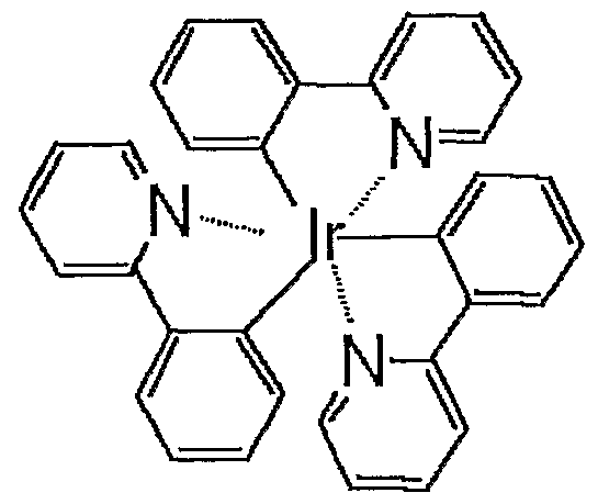
In recent years, there have been a number of studies in which phosphorescent compounds are used as a light-emitting material and the energy in a triplet state is used for an EL emission. A group of Princeton University has reported that an organic light-emitting device using an iridium complex as a light-emitting material exhibits a high light- emitting efficiency (Nature 395, 151 (1998)).
Moreover, a group of Cambridge University has reported (Nature 347, 539 (1990)) an organic light-
emitting device using a conjugated polymer other than the organic light-emitting device using monomeric materials as described above. In this report the light-emission in a monolayer is confirmed by forming a film of polyphenylenevinylene (PPV) in a coating system.
The related patents on organic light-emitting devices using conjugated polymers include U.S. Patent No. 5,247,190; U.S. Patent No. 5,514,878; U.S. Patent No. 5,672,678; U.S. Patent No. 5,317,169; U.S. Patent No. 5,726,457 and Japanese Patent Application Laid- Open No. H05-247460.
Thus, recent progress in organic light-emitting devices is remarkable, and possibilities for a wide range of applications are indicated since it is characterized in that a thin and light-weight light- emitting device having high luminance at a low applied-voltage, diversity of light-emitting wavelength and high-speed response can be prepared. However, a higher-luminance light output or high conversion efficiency is required under present circumstances. In addition, there are numbers of problems in terms of durability such as the variation with time during use for a long period of time and the deterioration due to an atmospheric gas containing oxygen or humidity. Moreover, the light- emission of blue, green and red having a good color
purity is required for applications such as a full- color display, but these issues are not sufficiently satisfied.
Aromatic compounds and condensed polycyclic aromatic compounds have been studied in great numbers as fluorescent organic compounds to be used for an electron-transporting layer or a light-emitting layer. These include, for example, Japanese Patent Application Laid-Open No. H04-68076; Japanese Patent Application Laid-Open No. H05-32966; Japanese Patent Application Laid-Open No. H06-228552; Japanese Patent Application Laid-Open No. H06-240244; Japanese Patent Application Laid-Open No. H07-109454; U.S. Patent No. 6,203,933; Japanese Patent Application Laid-Open No. H09-241629; U.S. Patent No. 6,387,547; U.S. Patent No. 6,399,223 and Japanese Patent Application Laid-Open No. 2000-268964. However, nothing that sufficiently satisfies light-emission luminance and durability has been obtained so far.
DISCLOSURE OF THE INVENTION
It is an object of the present invention to provide a new condensed polycyclic compound.
It is a further object of the present invention to provide an organic light-emitting device having a light output with an extremely high efficiency and high luminance using a specific condensed polycyclic
compound.
It is a further object of the present invention to provide an extremely durable organic light- emitting device. It is a further object of the present invention to provide an organic light-emitting device that is easily produced and can be prepared at a relatively low cost .
Specifically, the present invention provides a condensed polycyclic compound represented by general formula [I] or [II]:
wherein R
x is hydrogen, halogen, cyano, a substituted amino or a group selected from the group consisting of alkyl, aralkyl, aryl, heterocyclic, each having no substituent or a substituent; and Ar
x to Ar
5 are the same or different and are each independently a condensed polycyclic aromatic group or a condensed polycyclic heterocyclic group, each having no substituent or a substituent; and
wherein Ar6 to Arxl are the same or different and are each independently a group selected from the group consisting of condensed polycyclic aromatic groups and condensed polycyclic heterocyclic groups , each having no substituent or a substituent.
The present invention further provides an organic light-emitting device comprising a pair of electrodes consisting of an anode and a cathode and organic compound-containing layers sandwiched between the pair of electrodes, wherein at least one layer of the organic compound-containing layers contains at least one compound selected from the group consisting of the condensed polycyclic compounds.
BRIEF DESCRIPTION OF THE DRAWINGS
Fig. 1 is a sectional view illustrating one example of the organic light-emitting device according to the present invention;
Fig. 2 is a sectional view illustrating another example of the organic light-emitting device according to the present invention;
s Fig. 3 is a sectional view illustrating another example of the organic light-emitting device according to the present invention;
Fig. 4 is a sectional view illustrating another example of the organic light-emitting device according to the present invention;
Fig. 5 is a sectional view illustrating another example of the organic light-emitting device according to the present invention; and Fig. 6 is a sectional view illustrating another example of the organic light-emitting device according to the present invention.
BEST MODE FOR CARRYING OUT THE INVENTION The present invention will now be described in detail.
The condensed polycyclic compounds of the present invention will be first described.
The condensed polycyclic compounds of the present invention are represented by the above general formula [I] or [II].
Herein, at least one of Ar
x to Ar
s or at least one of Ar
6 to Ar
xl is preferably a condensed polycyclic aromatic group represented by general formula [III]:
wherein R2 is hydrogen, halogen, cyano, a substituted amino or a group selected from the group consisting of alkyl, aralkyl, aryl and heterocyclic, each having no substituent or a substituent; and R3 and R4 are the same or different and are each independently hydrogen or a group selected from the group consisting of alkyl, aralkyl, aryl and heterocyclic, each having no substituent or a substituent.
Further, the condensed polycyclic compounds of the present invention are more preferably represented by any of general formulas .
Furthermore, at least one of Ar
x to Ar
5 or at least one of Ar
6 to Ar
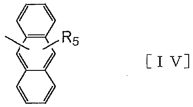
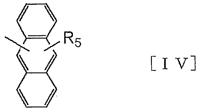
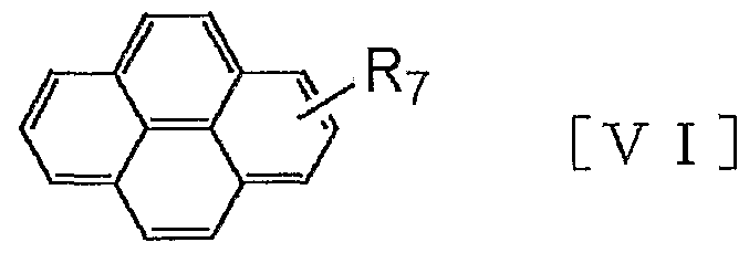
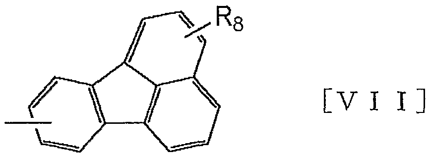
xl preferably denotes a condensed polycyclic aromatic group represented by any of general formulas [IV] to [VII]:
wherein R5 to R8 are hydrogen, halogen, cyano, a substituted amino or a group selected from the group
consisting of alkyl, aralkyl, aryl and heterocyclic, each having no substituent or a substituent.
Specific examples for the substituent groups in the above general formulas [I] to [VII] are shown below.
The alkyl group includes methyl, ethyl, n-propyl, iso-propyl, n-butyl, ter-butyl, octyl or the like.
The aralkyl group includes benzyl, phenethyl or the like . The aryl group includes phenyl, biphenyl, terphenyl or the like .
The heterocyclic group includes thienyl, pyrolyl, pyridyl, oxazolyl, oxadiazolyl, thiazolyl, thidiazolyl, terthienyl or the like. The substituted amino group includes dimethylamino, diehtylamino, dibenzylamino, diphenylamino, ditolylamino, dianisolylamino or the like.
The halogen atom includes fluorine, chlorine, bromine, iodine or the like.
The condensed polycyclic aromatic group includes fluorenyl, naphthyl, fluoranthenyl, anthryl, phenathryl, pyrenyl, tetracenyl, pentacenyl or the like. The condensed polycyclic heterocyclic group includes quinolyl, diazafluorenyl, acrydinyl, phenanthrolyl or the like.
The substituent groups that the above substituent groups may have include alkyl groups such as methyl, ethyl and propyl; aralkyl groups such as benzyl and phenethyl; aryl groups such as phenyl and biphenyl; heterocyclic groups such as thienyl, pyrolyl and pyridyl; amino groups such as dimethylamino, diethylamino , dibenzylamino, diphenylamino, ditolylamino and dianisolylamino; alkoxyl groups such as methoxyl, ethoxyl, propoxyl and phenoxyl; cyano group and halogen atoms such as fluorine, chlorine, bromine and iodine .
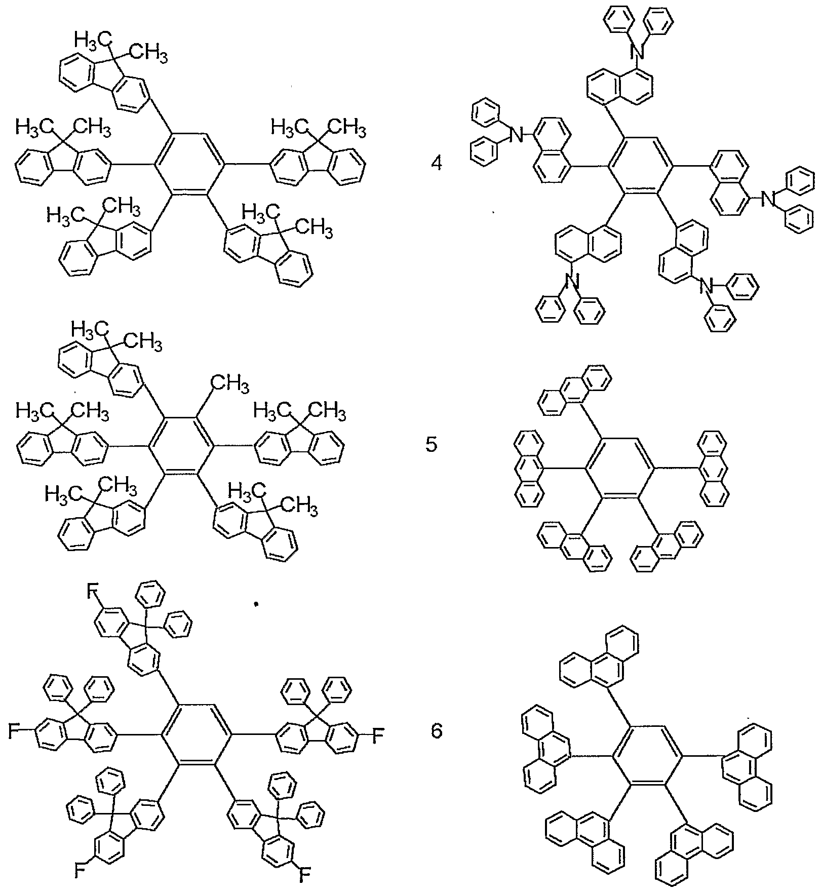
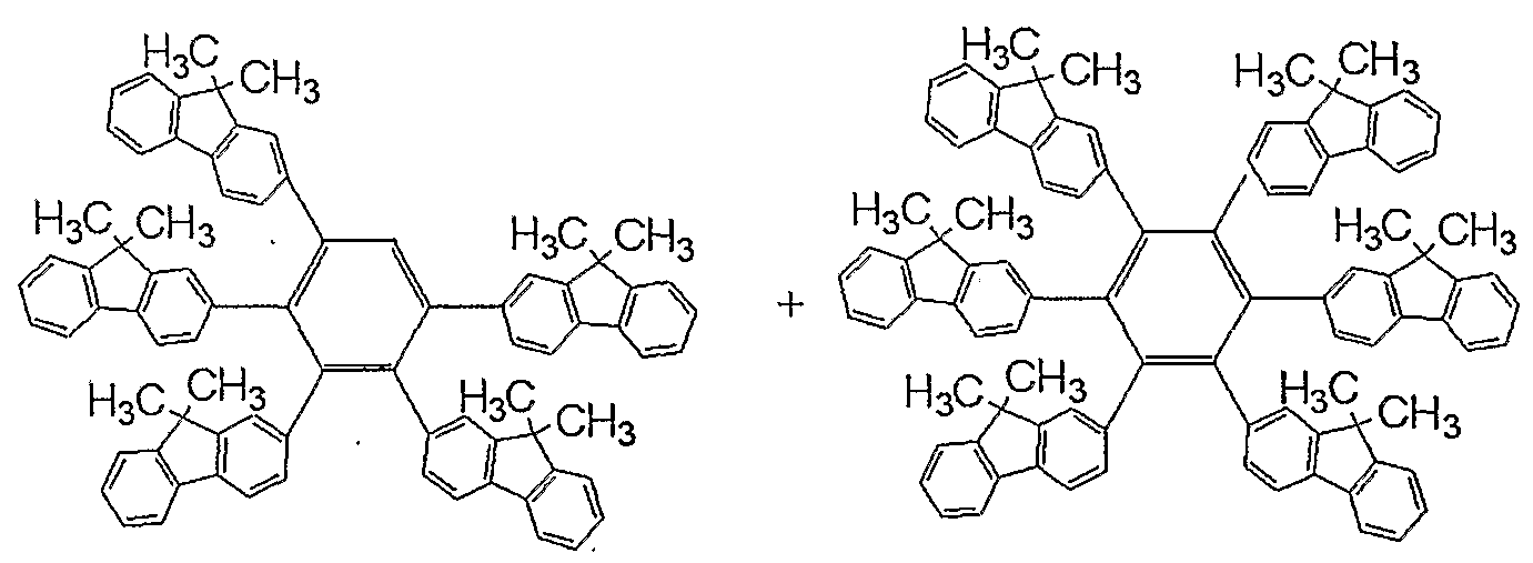
The followings are typical examples of the condensed polycyclic compounds of the present invention, but the present invention is not limited thereto:
The condensed polycyclic compounds of the present invention can be synthesized by generally known methods , and can be obtained by synthesis methods such as, for example, Suzuki coupling method using a palladium catalyst (e.g., Chem. Rev. 1995, 95, 2457-2483); Yamamoto method using a nickel catalyst
(e.g.. Bull. Chem. Soc. Jpn. 51, 2091, 1978) and a synthesizing method using aryltin compounds (e.g., J. Org. Chem., 52, 4296, 1987).
The condensed polycyclic compounds of the present invention are excellent in an electron- transporting property, a light-emitting property and durability compared with conventional compounds, and are useful for an organic compound-containing layer, in particular, an electron-transporting layer and a light-emitting layer in an organic light-emitting device. In addition, the layer formed by a vacuum deposition process or a solution coating process hardly causes crystallization or the like and is excellent in the stability with time. The organic light-emitting device of the present invention will now be described in detail.
The organic light-emitting device of the present invention at least comprises a pair of electrodes consisting of an anode and a cathode and one or a plurality of organic compound-containing layers sandwiched between the pair of electrodes , wherein at least one layer of the above-described organic compound-containing layers contains at least one compound selected from the group consisting of the condensed polycyclic compounds represented by the above general formula [I] or general formula [II]. In the organic light-emitting device of the
present invention, at least the electron transporting layer or the light-emitting layer among the organic compound-containing layers preferably contains at least one selected from the group consisting of the above-described condensed polycyclic compounds.
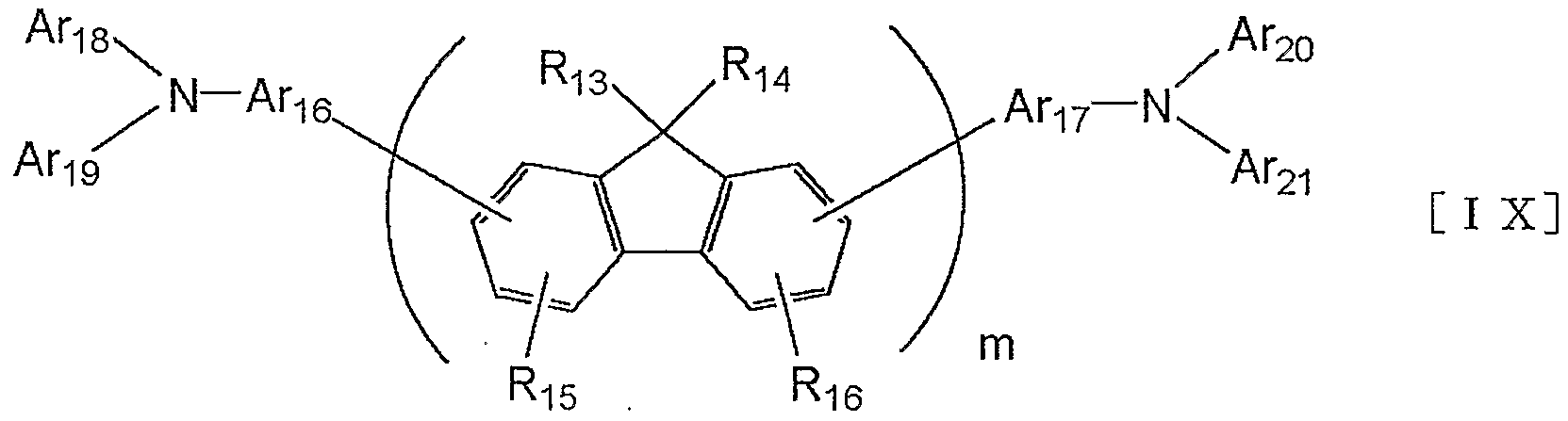
In the organic light-emitting device of the present invention, the condensed polycyclic compounds represented by the above general formula [ I ] or general formula [II] are formed between the anode and the cathode by a vacuum deposition process or a solution coating process. The organic layer is preferably formed in a thin film having a thickness of less than 10 μ.m, preferably 0.5 m or less, more preferably from 0.01 to 0.5 £tm. The organic light-emitting device of the present invention comprises a preferred embodiment that at least the light-emitting layer of the organic compound-containing layers contains at least one selected from the group consisting of the condensed polycyclic compounds and a fluorene compound represented by general formula [VIII] or [IX]:
wherein R
9 and R
10 are the same or different and are each independently hydrogen or a group selected from the group consisting of alkyl, aralkyl, aryl and heterocyclic, each having no substituent or a substituent; any pair of R
9 combined to their respective fluorene structures are the same or different to each other; any pair of R
10 combined to their respective fluorene structures are the same or different to each other; R
X1 and R
12 are the same or different and are each independently hydrogen, halogen, cyano or a group selected from the group consisting of alkyl, aralkyl, aryl and heterocyclic, each having no substituent or a substituent; any pair of R
1X combined to their respective fluorene structures are the same or different to each other; any pair of R
12 combined to their respective fluorene structures are the same or different to each other; Ar
12, Ar
13, Ar
14 and Ar
15 are the same or different and are each independently a group selected from the group consisting of aromatic, heterocyclic, condensed polycyclic aromatic and condensed polycyclic heterocyclic, each having no substituent or a substituent, and Ar
12 and Ar
14 can be bonded to Ar
13 and Ar
15 respectively to form a ring; and n is an integer from 1 to 10, and
wherein R13 and R14 are the same or different and are each independently hydrogen or a group selected from the group consisting of alkyl, aralkyl, aryl and heterocyclic, each having no substituent or a substituent ; any pair of R13 combined to their respective fluorene structures are the same or different to each other; any pair of R14 combined to their respective fluorene structures are the same or different to each other; R15 and R16 are the same or different and are each independently hydrogen, halogen, cyano or a group selected from the group consisting of alkyl, aralkyl, aryl and heterocyclic, each having no substituent or a substituent; any pair of R15 combined to their respective fluorene structures are the same or different to each other; any pair of R16 combined to their respective fluorene structures are the same or different to each other; Ar16 and Ar17 are the same or different and are each independently a divalent group selected from the group consisting of divalent aromatic and divalent heterocyclic, each having no substituent or a
substituent; Ar18, Ar19, Ar20 and Ar21 are the same or different and are each independently a group selected from the group consisting of aromatic, heterocyclic, condensed polycyclic aromatic and condensed polycyclic heterocyclic, each having no substituent or a substituent , and Ar18 and Ar20 can be bonded to Ar19 and Ar21 respectively to form a ring; and m is an integer from 1 to 10.
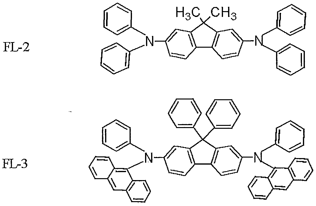
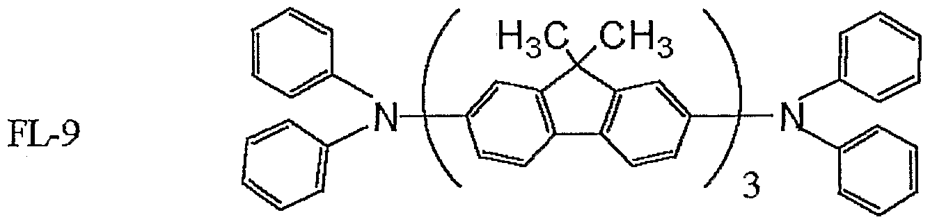
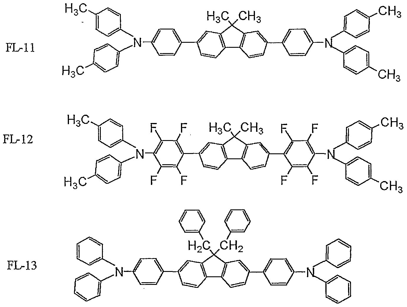
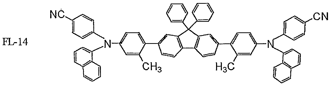
Examples of the substituent groups in the general formulas [VIII] and [IX] are similar to those in the above general formulas [I] to [VII] . The followings are typical examples of the fluorene compounds represented by the general formula [VIII] or [IX], but the present invention is not limited thereto:
Figs . 1 to 6 illustrate preferred examples of the organic light-emitting devices of the present invention .
The example of Figure 1 has the structure in which an anode 2, a light-emitting layer 3 and a cathode 4 are provided on a substrate 1 in this order.
The light-emitting device herein used is useful when it has a hole-transporting capability, an electron- transporting capability and light-emitting performance singly within itself , or when compounds having respective characteristics are mixed for use.
The example of Fig. 2 has the structure in which an anode 2, a hole-transporting layer 5, an electron- transporting layer 6 and a cathode 4 are provided on a substrate 1 in this order. This example is useful when a material having a hole-transporting capability and/or an electron-transporting capability is used for respective layers as a light-emitting substance in combination with a mere hole-transporting substance or an electron-transporting substance having no light-emitting property. In this case, the light-emitting layer comprises the hole-transporting layer 5 or the electron-transporting layer 6.
The example of Fig. 3 has the structure in which an anode 2, a hole-transporting layer 5, a light- emitting layer 3, an electron-transporting layer 6 and a cathode 4 are provided on a substrate 1 in this order, a carrier-transporting function and a light- emitting function being separated. The separation of the light-emitting layer from the charge-transporting layer extremely increases the freedom of material selection since a compound having each property such as a hole-transporting property, an electron-
transporting property or a light-emitting property can be used in a suitable combination. For example, various compounds having different light-emitting wavelengths can be used to allow diversification of the hue of light emission. Further, it is also possible to try to improve the efficiency of light emission by effectively confining each carrier or exciton in the central light-emitting layer 3.
The example of Fig. 4 has the structure in which a hole-injecting layer 7 is inserted between the anode 2 and the hole-transporting layer 5 in the form of Fig. 3, which is effective for improving adhesiveness of the anode 2 to the hole-transporting layer 5 or to improve a hole-injecting property, being effective to reduce voltage.
Examples of Figs . 5 and 6 have the structure in which a layer for blocking a hole or an exciton from passing through to the side of the cathode 4 (hole- blocking layer 8) is inserted between the light- emitting layer 3 and the electron-transporting layer 6 in the forms of Figs . 3 and 4. The use of a compound having a very high ionization potential as the hole-blocking layer 8 is effective for improving the efficiency of light-emission. Figs. 1 to 6 are very basic device structures, and the structures of the organic light-emitting device using the compounds of the present invention
are not limited to these. It is possible to take the structure of diversified layers, for example, to provide an insulating layer to the interface between the electrodes and the organic layers, to provide an adhesion layer or an interference layer or to compose a hole-transporting layer from two layers having different ionization potentials.
The condensed polycyclic compounds represented by the general formula [I] or the general formula [II] used in the present invention are excellent in an electron-transporting property, a light-emitting property and durability compared with conventional compounds , and can be used in any forms shown in Figures 1 to 6. Although the present invention uses the condensed polycyclic compounds represented by the general formula [I] or the general formula [II] as constituent components for the electron-transporting layer or the light-emitting layer, already known hole-transporting compounds, light-emitting compounds or electron-transporting compounds can also be used together as necessary.
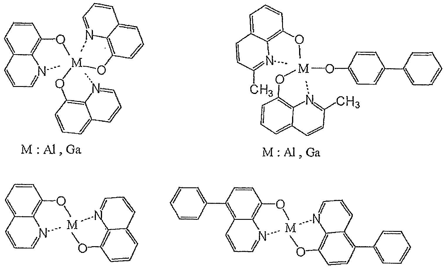
Examples of these compounds include the followings :
Hole-transporting compounds
M : Cu, Mg, AlCl, TiO, SiCl2, Zn Sn, m-MTDATA JVlnCl, GaCI, etc
TPAC PDA
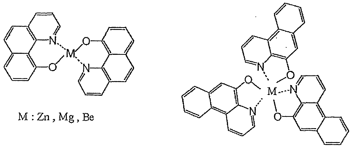
Electron-transporting light-emitting materials
M : Zn , Mg , Be M : Zn , M , Be
M : Zn , Mg , Be M : Zn , Mg , Be
M : Al , Ga
Light-emitting materials
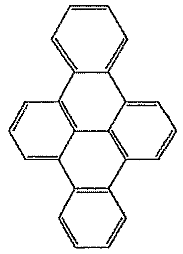
Quinacridone
Coronene
Light-emitting layer matrix materials and electron- transporting materials
Polymer-based hole-transporting materials
TPD-PCA
Poly thiophene Polysilane
Polymer-based light-emitting materials and charge- transporting materials
In the organic light-emitting device of the present invention, the layers containing the condensed polycyclic compounds represented by the general formula [I] or the general formula [II] and the layers containing other organic compounds are generally formed into thin films by a vacuum deposition process or a coating process in which they are dissolved in a suitable solvent. In particular.
when the film is formed by a coating process, it is also possible to form the film in combination with suitable binding resins.
The above-described binding resins can be selected from a wide range of binding resins , and include, but not limited to, polyvinylcarbazole resins, polycarbonate resins, polyester resins, polyallylate resins, polystyrene resins, acrylic resins, methacrylic resins, butyral resins, polyvinylacetal resins, diallylphthalate resins, phenol resins, epoxy resins, silicone resins, polysulfone resins, urea resins and the like. In addition, one of them or a mixture of two or more of them may be used in the form of a homopolymer or a copolymer.
The materials for the anode preferably have a large work function, and elemental metals such as gold, platinum, nickel, palladium, cobalt, serene, vanadium and alloys thereof and metal oxides such as tin oxides, zinc oxides, indium tin oxides (ITO) and indium zinc oxides can be used. In addition, conductive polymers such as polyaniline, polypyrrole, polythiophene and poyphenylene sulfide can be used. These electrode materials can be used singly or in combination.
On the other hand, the materials for the cathode preferably have a small work function, and elemental
metals such as lithium, sodium, potassium, calcium, magnesium, aluminum, indium, silver, lead, tin and chrome and alloys thereof can be used. Metal oxides such as indium tin oxides (ITO) can also be used. The cathode may have one-layered structure or may have a multilayered structure .
The substrates for use in the present invention include, but not limited to, metal substrates, opaque substrates such as ceramic substrates , transparent substrates such as glass, quartz and plastic sheet. Moreover, it is possible to control the color of emitted light using a color filter film, a fluorescent color conversion filter film, a dielectric reflecting film and the like for the substrate.
Furthermore, a protective layer or a sealing layer can also be provided to the prepared device for the purpose of preventing contact with oxygen, moisture and the like . The protective layer includes an inorganic material film such as a diamond thin film, a metal oxide or a metal nitride; a polymeric film such as a fluororesin, polyparaxylene, polyethylene, a silicone resin and a polystyrene resin; a photo-curable resin or the like. Moreover, the device itself can be covered with glass, a gas- impermeable film, metal or the like and packaged with a suitable sealing resin.
( Examples )
The present invention will now be described in detail with reference to examples , but the present invention is not limited to them. <Example of synthesis 1> (Synthesis of the illustrated compounds No. 1 and No. 11)
No.l
No.11
To a three-necked flask of 500 ml, 1.4 g (2.54 mmol) of hexabromobenzene [1], 6.0 g (25.4 mmol) of 9 , 9-dimethylfluorene-2-boronic acid [2], 160 ml of toluene and 80 ml of ethanol were charged and an aqueous solution of 30 g of sodium carbonate/150 ml of water was dropped under stirring at room temperature in a nitrogen atmosphere, and then 0.9 g (0.78 mmol) of tetrakis(triphenylphosphine)palladium
(0) was added. After stirring at room temperature for 30 minutes, the mixture was raised to a temperature of 77°C and stirred for 20 hours. After the reaction was completed, the organic layer was extracted with chloroform, dried with anhydrous sodium sulfate and purified with a silica gel column (hexane + toluene mixed developing solvent), obtaining 0.44 g (yield of 17%) of the illustrated compound No. 1 (white crystal) and 1.3 g (yield of 42%) of No. 11 (white crystal) .
<Example of synthesis 2> (Synthesis of the illustrated compound No. 2)
No.2
To a three-necked flask of 300 ml, 0.5 g (1.03 mmol) of 2,3,4,5,6-pentabromotoluene [1], 2.5 g (10.3 mmol) of 9,9-dimethylfluorene-2-boronic acid [2], 100 ml of toluene and 50 ml of ethanol were charged and an aqueous solution of 10 g of sodium carbonate/50 ml of water was dropped under stirring at room
temperature in a nitrogen atmosphere, and then 0.3 g (0.26 mmol) of tetrakis (triphenylphosphine)palladium (0) was added. After stirring at room temperature for 30 minutes, the mixture was raised to a temperature of 7°C and stirred for 20 hours. After the reaction, the organic layer was extracted with chloroform before dried with anhydrous sodium sulfate and purified with a silica gel column (hexane + toluene mixed developing solvent), obtaining 0.54 g (yield of 55%) of the illustrated compound No. 2 (white crystal) . <Example 1>
A device having the structure shown in Figure 2 was prepared. On a glass substrate as the substrate 1, indium tin oxide (ITO) as the anode 2 was deposited by a sputtering process in a thickness of 120 nm and ultrasonically cleaned with acetone and isopropyl alcohol (IPA) in this order, and dried after the cleaning by boiling with IPA. Further, it was cleaned with UV/ozone. The resultant structure is referred to a transparent conductive supporting substrate. On the transparent conductive supporting substrate, a 0.5% by weight chloroform solution of the compound represented by the following structural formula was applied by a spin-coating process to form a film having a thickness of 30 nm, forming the hole-
transporting layer 5.
The condensed polycyclic compound represented by the illustrated compound No. 11 was deposited on the hole-transporting layer 5 by a vacuum deposition process in a thickness of 50 nm to form the electron- transporting layer 6. As for the conditions , the degree of the vacuum at the vapor deposition was 1.0 x 10"4 Pa and the speed of deposition was 0.2 to 0.3 nm/sec.
A vapor deposition material consisting of aluminum and lithium (lithium concentration of 1 atomic %) was used to form a metal layer film having a thickness of 50 nm on the electron-transporting layer 6 by a vacuum deposition process, and further by the vacuum deposition process an aluminum layer having a thickness of 150 nm was provided to form the cathode 4. As for the conditions, the degree of the
vacuum at the vapor deposition was 1.0 x 10⁴ Pa and the speed of deposition was 1.0 to 1.2 nm/sec.
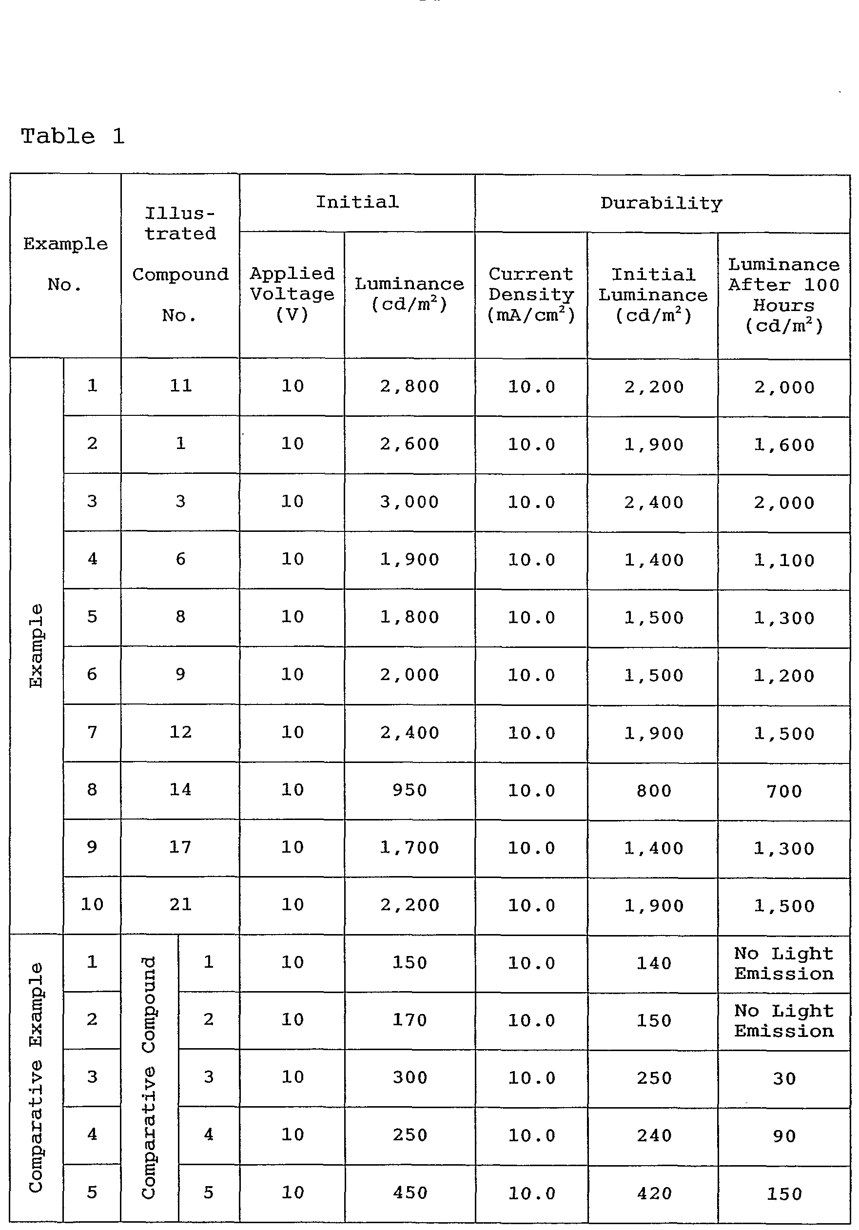
The resultant structure was covered with a protective glass plate in a nitrogen atmosphere and sealed with an acrylic resin-based adhesive material. When the thus obtained organic EL device was applied with a direct-current voltage of 10 V using an ITO electrode (anode 2) as a positive electrode and an Al-Li electrode (cathode 4) as a negative electrode, the current passed through the device at a current density of 12.0 mA/cm2 and the light emission of blue color was observed at a luminance of 2,800 cd/m2.
In addition, when the voltage was applied for 100 hours while maintaining the current density at 10.0 mA/cm2, the initial luminance of 2,200 cd/m2 dropped to 2,000 cd/m2 after 100 hours, exhibiting only a small reduction of luminance. <Examples 2 to 10> Devices were prepared and evaluated in the same manner as in Example 1 except that illustrated compounds shown in Table 1 replaced the illustrated compound No. 11. The results are shown in Table 1. <Comparative Examples 1 to 5> Devices were prepared and evaluated in the same manner as in Example 1 except that the compounds represented by the structural formulas below replaced
the illustrated compound No. 11. The results are shown in Table 1. Comparative compound No . 1
Comparative compound No. 2
Comparative compound No. 3
Comparative compound No. 4.
Comparative compound No. 5
<Example 11>
The device shown in Figure 3 was prepared.
The hole-transporting layer 5 was formed on the transparent conductive supporting substrate in the same manner as in Example 1.
The condensed polycyclic compound represented by the illustrated compound No. 1 was deposited on the hole-transporting layer 5 by a vacuum deposition process in a thickness of 20 nm to form the light- emitting layer 3. As for the conditions, the degree of the vacuum at the vapor deposition was 1.0 x 10~4 Pa and the speed of deposition was 0.2 to 0.3 nm/sec.
Aluminum-trisquinolinol was deposited on the light-emitting layer 3 by a vacuum deposition process in a thickness of 40 nm to form the electron- transporting layer 6. As for the conditions , the degree of the vacuum at the vapor deposition was 1.0 x 10"4 Pa and the speed of deposition was 0.2 to 0.3 nm/sec. The device was sealed after the cathode 4 was formed in the same manner as in Example 1.
When the thus obtained device was applied with a direct-current voltage of 8 V using an ITO electrode
(anode 2) as a positive electrode and an Al-Li electrode (cathode 4) as a negative electrode, the current having a current density of 14.0 mA/cm2 passed through the device and the light emission of blue
color was observed at a luminance of 5,800 cd/m2.
In addition, when the voltage was applied for 100 hours while maintaining the current density at 10.0 mA/cm2, the initial luminance of 4,500 cd/m2 dropped to 4,200 cd/m2 after 100 hours, exhibiting only a small reduction of luminance. <Examples 12 to 20>
Devices were prepared and evaluated in the same manner as in Example 11 except that illustrated compounds shown in Table 2 replaced the illustrated compound No. 1. The results are shown in Table 2. <Comparative Examples 6 to 10>
Devices were prepared and evaluated in the same manner as in Example 11 except that the comparative compounds No. 1 to 5 replaced the illustrated compound No. 1. The results are shown in Table 2.
<Example 21>
The device shown in Figure 3 was prepared.
On the transparent conductive supporting substrate similar to that in Example 1, a 0.5% by weight chloroform solution of the compound represented by the following structural formula was applied by a spin-coating process to form a film having a thickness of 20 nm, forming the hole- transporting layer 5.
In addition, the condensed polycyclic compound represented by the illustrated compound No. 11 and the fluorene compound represented by the illustrated compound No. FL-6 (weight ratio of 100:1) were deposited by a vacuum deposition process in a thickness of 20 nm to form the light-emitting layer 3 As for the conditions, the degree of the vacuum at the vapor deposition was 1.0 x 10~4 Pa and the speed of deposition was 0.2 to 0.3 nm/sec.
Moreover, aluminum-trisquinolinol was deposited by a vacuum deposition process in a thickness of 40
nm to form the electron-transporting layer 6. As for the conditions for deposition, the degree of the vacuum at the vapor deposition was 1.0 x 10"4 Pa and the speed of deposition was 0.2 to 0.3 nm/sec. , The device was then sealed after the cathode 4 was formed in the same manner as in Example 1.
When the thus obtained device was applied with a direct-current voltage of 8 V using an ITO electrode (anode 2) as a positive electrode and an Al-Li electrode (cathode 4) as a negative electrode, the current passed through the device at a current density of 13.0 mA/cm2 and the light emission of blue color was observed at a luminance of 13,000 cd/m2. In addition, when the voltage was applied for 100 hours while maintaining the current density at 10.0 mA/cm2, the initial luminance of 10,000 cd/m2 dropped to 8,900 cd/m2 after 100 hours, exhibiting only a small reduction of luminance. <Examples 22 to 40> Devices were prepared and evaluated in the same manner as in Example 21 except that illustrated fluorene compounds shown in Table 3 replaced the illustrated fluorene compound No. FL-6. The results are shown in Table 3. <Comparative Examples 11 to 15>
Devices were prepared and evaluated in the same manner as in Example 21 except that the comparative
compounds No. 1 to 5 replaced the illustrated compound No. 11. The results are shown in Table 3.
<Example 41>
The device shown in Figure 3 was prepared.
On the transparent conductive supporting substrate similar to that in Example 1, a 0.5% by weight chloroform solution of the compound represented by the following structural formula was applied by a spin-coating process to form a film having a thickness of 20 nm, forming the hole- transporting layer 5.
In addition, the condensed polycyclic compound represented by the illustrated compound No . 2 and the compound represented by the following structural formula (weight ratio of 100:5) were deposited by a vacuum deposition process in a thickness of 20 nm to form the light-emitting layer 3. As for the conditions for deposition, the degree of the vacuum at the vapor deposition was 1.0 x 10"4 Pa and the speed of deposition was 0.2 to 0.3 nm/sec.
Moreover, bathophenanthroline (BPhen) was deposited by a vacuum deposition process in a thickness of 40 nm to form the electron-transporting layer 6. As for the conditions for deposition, the degree of the vacuum at the vapor deposition was 1.0 x 10"4 Pa and the speed of deposition was 0.2 to 0.3 nm/sec. The device was then sealed after the cathode 4 was formed in the same manner as in Example 1.
When the thus obtained device was applied with a direct-current voltage of 8 V using an ITO electrode (anode 2) as a positive electrode and an Al-Li electrode (cathode 4) as a negative electrode, the current passed through the device at a current density of 9.5 mA/cm2 and the light emission of green color was observed at a luminance of 7,000 cd/m2.
In addition, when the voltage was applied for 100 hours while maintaining the current density at 7.0 mA/cm2, the initial luminance of 5,000 cd/m2 dropped to 4,500 cd/m2 after 100 hours, exhibiting only a small reduction of luminance.
<Examples 42 to 50>
Devices were prepared and evaluated in the same manner as in Example 41 except that illustrated compounds shown in Table 4 replaced the illustrated compound No. 2. The results are shown in Table 4. <Comparative Examples 16 to 20>
Devices were prepared and evaluated in the same manner as in Example 41 except that the comparative compounds No. 1 to 5 replaced the illustrated compound No. 2. The results are shown in Table 4.
<Example 51>
The device shown in Figure 1 was prepared. On the transparent conductive supporting substrate similar to that in Example 1, a solution in which 0.050 g of the condensed polycyclic compound represented by the illustrated compound No. 1 and 1.00 g of poly-N-vinylcarbazole (weight average molecular weight = 63,000) were dissolved in 80 ml of chloroform was applied by a spin-coating process (the number of revolutions = 2,000 rpm) to form a film having a thickness of 120 nm, forming the organic layer (light-emitting layer 3).
The device was then sealed after the cathode 4 was formed in the same manner as in Example 1. When the thus obtained device was applied with a direct-current voltage of 10 V using an ITO electrode (anode 2 ) as a positive electrode and an Al-Li electrode (cathode 4) as a negative electrode, the current passed through the device at a current density of 7.7 mA/cm2 and the light emission of blue color was observed at a luminance of 1,400 cd/m2.
In addition, when the voltage was applied for 100 hours while maintaining the current density at 5.0 mA/cm2 in a nitrogen atmosphere, the initial luminance of 950 cd/m2 dropped to 900 cd/m2 after 100 hours, exhibiting only a small reduction of luminance. <Examples 52 to 55>
Devices were prepared and evaluated in the same manner as in Example 51 except that illustrated compounds shown in Table 5 replaced the illustrated compound No . 1. The results are shown in Table 5. <Comparative Examples 21 to 25>
Devices were prepared and evaluated in the same manner as in Example 51 except that the comparative compounds No . 1 to 5 replaced the illustrated compound No . 1. The results are shown in Table 5.
Table 5
As described above by illustrating embodiments and examples, the organic light-emitting devices using the condensed polycyclic compounds represented by the general formula [I] or the general formula [II] provide the light-emission having high luminance at a low applied voltage and are also excellent in durability. Particularly, the organic layers containing the condensed polycyclic compounds of the
present invention are excellent as an electron- transporting layer as well as a light-emitting layer. Moreover, it is possible to prepare the devices by using a vacuum deposition process, casting process or the like, and the devices having a large area can be prepared easily at a relatively low cost.