US8810144B2 - Driver circuits for dimmable solid state lighting apparatus - Google Patents
Driver circuits for dimmable solid state lighting apparatus Download PDFInfo
- Publication number
- US8810144B2 US8810144B2 US13/462,388 US201213462388A US8810144B2 US 8810144 B2 US8810144 B2 US 8810144B2 US 201213462388 A US201213462388 A US 201213462388A US 8810144 B2 US8810144 B2 US 8810144B2
- Authority
- US
- United States
- Prior art keywords
- voltage
- coupled
- node
- charging
- control
- Prior art date
- Legal status (The legal status is an assumption and is not a legal conclusion. Google has not performed a legal analysis and makes no representation as to the accuracy of the status listed.)
- Active
Links
Images


Classifications
-
- H—ELECTRICITY
- H05—ELECTRIC TECHNIQUES NOT OTHERWISE PROVIDED FOR
- H05B—ELECTRIC HEATING; ELECTRIC LIGHT SOURCES NOT OTHERWISE PROVIDED FOR; CIRCUIT ARRANGEMENTS FOR ELECTRIC LIGHT SOURCES, IN GENERAL
- H05B45/00—Circuit arrangements for operating light-emitting diodes [LED]
- H05B45/30—Driver circuits
- H05B45/37—Converter circuits
- H05B45/3725—Switched mode power supply [SMPS]
- H05B45/38—Switched mode power supply [SMPS] using boost topology
-
- H—ELECTRICITY
- H02—GENERATION; CONVERSION OR DISTRIBUTION OF ELECTRIC POWER
- H02M—APPARATUS FOR CONVERSION BETWEEN AC AND AC, BETWEEN AC AND DC, OR BETWEEN DC AND DC, AND FOR USE WITH MAINS OR SIMILAR POWER SUPPLY SYSTEMS; CONVERSION OF DC OR AC INPUT POWER INTO SURGE OUTPUT POWER; CONTROL OR REGULATION THEREOF
- H02M3/00—Conversion of DC power input into DC power output
- H02M3/22—Conversion of DC power input into DC power output with intermediate conversion into AC
- H02M3/24—Conversion of DC power input into DC power output with intermediate conversion into AC by static converters
- H02M3/28—Conversion of DC power input into DC power output with intermediate conversion into AC by static converters using discharge tubes with control electrode or semiconductor devices with control electrode to produce the intermediate AC
- H02M3/325—Conversion of DC power input into DC power output with intermediate conversion into AC by static converters using discharge tubes with control electrode or semiconductor devices with control electrode to produce the intermediate AC using devices of a triode or a transistor type requiring continuous application of a control signal
- H02M3/335—Conversion of DC power input into DC power output with intermediate conversion into AC by static converters using discharge tubes with control electrode or semiconductor devices with control electrode to produce the intermediate AC using devices of a triode or a transistor type requiring continuous application of a control signal using semiconductor devices only
- H02M3/33507—Conversion of DC power input into DC power output with intermediate conversion into AC by static converters using discharge tubes with control electrode or semiconductor devices with control electrode to produce the intermediate AC using devices of a triode or a transistor type requiring continuous application of a control signal using semiconductor devices only with automatic control of the output voltage or current, e.g. flyback converters
-
- H—ELECTRICITY
- H03—ELECTRONIC CIRCUITRY
- H03K—PULSE TECHNIQUE
- H03K5/00—Manipulating of pulses not covered by one of the other main groups of this subclass
- H03K5/153—Arrangements in which a pulse is delivered at the instant when a predetermined characteristic of an input signal is present or at a fixed time interval after this instant
- H03K5/1536—Zero-crossing detectors
-
- H—ELECTRICITY
- H05—ELECTRIC TECHNIQUES NOT OTHERWISE PROVIDED FOR
- H05B—ELECTRIC HEATING; ELECTRIC LIGHT SOURCES NOT OTHERWISE PROVIDED FOR; CIRCUIT ARRANGEMENTS FOR ELECTRIC LIGHT SOURCES, IN GENERAL
- H05B45/00—Circuit arrangements for operating light-emitting diodes [LED]
- H05B45/30—Driver circuits
- H05B45/37—Converter circuits
- H05B45/3725—Switched mode power supply [SMPS]
Definitions
- the present inventive concept relates to driver circuits for solid state lighting apparatus.
- Solid-state lighting arrays are used for a number of lighting applications.
- solid-state lighting panels including arrays of solid-state light emitting devices have been used as direct illumination sources, for example, in architectural and/or accent lighting.
- a solid-state light emitting device may include, for example, a packaged light emitting device including one or more light emitting diodes (LEDs), which may include inorganic LEDs, which may include semiconductor layers forming p-n junctions and/or organic LEDs (OLEDs), which may include organic light emission layers.
- LEDs light emitting diodes
- OLEDs organic LEDs
- a solid-state light emitting device generates light through the recombination of electronic carriers, i.e. electrons and holes, in a light emitting layer or region.
- a solid-state light emitting device may include, for example, a packaged light emitting device including one or more light emitting diodes (LEDs).
- Cree, Inc. produces a variety of recessed downlights, such as the LR-6 and CR-6, which use LEDs for illumination.
- Solid-state lighting panels are also commonly used as backlights for small liquid crystal display (LCD) screens, such as LCD display screens used in portable electronic devices, and for larger displays, such as LCD television displays.
- LCD liquid crystal display
- Solid state lighting devices are typically powered with a DC signal. However, power is conventionally delivered in AC form. It is therefore generally desirable for a solid state light fixture to include an AC/DC converter to convert AC line voltage to a DC voltage.
- Boost converters can be used to generate DC voltage from an AC line voltage with high power factor and low total harmonic distortion.
- the voltage of an LED-based load may be higher than the peak of the input (line) AC voltage.
- a single-stage boost converter can be employed as the driver, achieving high power efficiency and low cost.
- a power factor corrected (PFC) boost converter which converts 120V ac, 60 Hz, to 200-250V dc output could be used to drive an array of high-voltage (HV) LEDs at a power level of 10-15 W.
- Phase-cut dimmers are commonly used to reduce input power to conventional incandescent lighting fixtures, which causes the fixtures to dim. Phase-cut dimmers only pass a portion of the input voltage waveform in each cycle. Thus, during a portion of a phase-cut AC input signal, no voltage is provided to the fixture.
- Compatibility with phase cut dimming signals is also feasible for LED drivers based on boost converters.
- One low cost approach is to use open-loop control, which means a driver will not respond to the LED current decrease due to phase cut dimming, but rather keep the preset input current during dimmer conduction time. In this way, a ‘natural’ dimming performance is achieved, and input power, and thus LED current will reduce as the dimmer conduction time decreases.
- One other approach is for drivers to use closed-loop control. As control loops are complete and in effect, these drivers will try to compensate the input power decrease due to dimmer phase cut. In order to dim LEDs in these cases, the control loops should be saturated so that the input current cannot increase. The control loop saturation can be realized by clamping the output of an error amplifier, for example.
- phase cut dimming is for the boost converter to generate the bias voltage that is used to power the control circuits of the boost converter (so-called “housekeeping power”) during deep dimming.
- Conventional LED driver circuits draw housekeeping power from the auxiliary winding of a boost circuit inductor.
- the control circuits can lose power. This can cause the entire driver circuit to cut off, which can result in visible flicker of the solid state lighting apparatus or other issues.
- a voltage regulator includes a charging switch including a first terminal coupled to a high voltage node, a second terminal, and a control terminal, a rectifier coupled to the second terminal of the charging switch, an output capacitor coupled to the rectifier, a control switch coupled to the second terminal, and a control voltage regulation circuit coupled to the control terminal of the charging switch.
- the control switch and the charging switch are configured so that when the control switch is turned off, a rise in voltage on the control switch causes an increase in voltage on the control terminal of the charging switch sufficient to allow a charging current to flow through the rectifier and into the output capacitor.
- the control voltage regulation circuit is configured to dissipate the increased voltage on the control switch so that the charging current only flows for a limited period of time in response to the control switch being turned off.
- the control voltage regulation circuit may include a clamping diode coupled to the control terminal of the charging switch.
- the voltage regulator may further include a resistor in parallel with the clamping diode and configured to allow a voltage clamped by the clamping diode to dissipate.
- a resistance of the resistor is selected to provide a desired pulse width of the charging current.
- the control switch has a parasitic capacitance that is charged when the control switch is turned off thereby causing the rise in voltage on the control switch.
- the control voltage regulation circuit may include a Zener diode coupled to a voltage node, a first resistor coupled between the voltage node and a voltage source, a clamping diode coupled to the control terminal of the charging switch, a second resistor coupled in parallel with the clamping diode, a third resistor coupled between the clamping diode and the voltage node, and a capacitor coupled to the voltage node.
- the second and third resistors and the capacitor may be configured to dissipate the increased voltage on the control terminal of the charging switch.
- the charging switch is configured to turn off in response to dissipation of the increased voltage on the control terminal of the charging switch.
- the voltage regulator may further include a main inductor, a zero crossing detection (ZCD) circuit configured to generate a zero cross detection signal in response to current through the main inductor falling to zero, and a control circuit configured to selectively activate the control switch in response to the zero cross detection signal.
- the zero crossing detection signal is configured to generate the zero cross detection signal to have a sufficient voltage swing to trigger a zero cross detection by the control circuit.
- the zero crossing detection circuit may include a capacitor coupled to the high voltage node and to a first node, a first resistor coupled to the capacitor and to a ZCD output node, a second resistor coupled to the ZCD output node, a first diode including an anode coupled to the first node and including a cathode, a second resistor coupled to the cathode of the diode, and a second diode including a cathode coupled to the second resistor.
- the zero crossing detection circuit may include a first resistor coupled to the high voltage node, a first Zener diode having a cathode coupled to the first resistor and having an anode coupled to a ZCD output node, a second Zener diode having a cathode coupled to the ZCD output node, a second resistor coupled to the ZCD output node, and a capacitor coupled to the ZCD output node.
- Some embodiments provide a voltage regulator for generating a housekeeping voltage in a power supply circuit.
- the voltage regulator includes a charging switch coupled to a high voltage node and to an output capacitor, and a control voltage regulation circuit coupled to a control terminal of the charging switch.
- the control switch and the charging switch are configured so that when the control switch is turned off, a rise in voltage on the control switch causes an increase in voltage on the control terminal of the charging switch sufficient to allow a charging current to flow into the output capacitor.
- the control voltage regulation circuit is configured to dissipate the increased voltage on the control switch so that the charging current only flows for a limited period of time in response to a state transition of the control switch.
- a voltage regulator for generating a housekeeping voltage in a power supply circuit includes a charging switch coupled to a high voltage node and to an output capacitor, and a control voltage regulation circuit coupled to the charging switch and configured to cause the charging switch to generate a current pulse for charging the output capacitor in response to a control signal.
- a method of generating a low voltage in a high voltage power supply includes generating a high voltage at a voltage node, and in response to a change in a voltage level at the voltage node, generating a pulse of current for charging an output capacitor to a level that is lower than the high voltage.
- FIG. 1 is a circuit diagram of a linear voltage regulator that can be used to generate a control circuit voltage.
- FIG. 2 is a circuit diagram of a voltage regulator circuit according to embodiments of the inventive concepts that can be used to generate a control circuit voltage.
- FIG. 3 is a graph of waveforms associated with the voltage regulator circuit shown in FIG. 2 .
- FIG. 4 is a block diagram of a zero cross detection circuit.
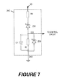
- FIGS. 5-7 are circuit diagrams of zero cross detection circuits according to embodiments of the inventive concepts.
- a lighting apparatus can be a device which illuminates an area or volume, e.g., a structure, a swimming pool or spa, a room, a warehouse, an indicator, a road, a parking lot, a vehicle, signage, e.g., road signs, a billboard, a ship, a toy, a mirror, a vessel, an electronic device, a boat, an aircraft, a stadium, a computer, a remote audio device, a remote video device, a cell phone, a tree, a window, an LCD display, a cave, a tunnel, a yard, a lamppost, or a device or array of devices that illuminate an enclosure, or a device that is used for edge or back-lighting (e.g., back light poster, signage, LCD displays), bulb replacements (e.g., for replacing AC incandescent lights, low voltage lights, fluorescent lights
- Some embodiments of the invention provide electronic circuits that address various needs in a dimmable LED driver circuit and/or that enable a wide range of dimming (e.g., down to 1%) with low-cost components.
- Embodiments of the invention are described herein in connection with a boost (step-up) converter.
- the invention is not limited to boost converters and may be used in connection with other types of circuits, such as, for example, buck (step-down), buck-boost, SEPIC, and/or other switch-mode power supply topologies and/or other voltage converter topologies.
- some embodiments instead of drawing the control circuit voltage from the auxiliary winding of a boost converter inductor, some embodiments generate a DC housekeeping voltage from a high voltage level found in the boost converter, such as a rectified line voltage.
- the rectified line voltage may be substantially higher than the voltage level needed to power the driver circuitry (e.g., 150 V vs 15 V). This difference in voltage may result in undesirable losses in the control voltage generation circuit.
- FIG. 1 a linear voltage regulator having a cascoded switch topology that can be used to generate a relatively low control circuit voltage is illustrated in FIG. 1 .
- the function of the circuit is to generate a relatively low bias “housekeeping” voltage VDD (typically about 15 V) from a high-voltage source VD (e.g., 150 V), which can be a rectified line voltage, as noted above.
- VDD relatively low bias “housekeeping” voltage
- VD e.g. 150 V
- the linear voltage regulator circuit shown in FIG. 1 includes a Zener diode ZD 1 , a resistor R 1 , a charging switch Q 1 , a diode D 1 and an output capacitor C 1 .
- the Zener diode ZD 1 and the resistor R 1 form a gate voltage regulation circuit that supplies a gate voltage equal to the Zener voltage of the Zener diode to the gate of the charging switch Q 1 .
- the charging switch Q 1 is illustrated as a MOSFET transistor switch in FIG. 1 . However, it will be appreciated that other types of transistor switches, such as bipolar junction transistors, can be used instead.
- a DC voltage VG is generated through the resistor R 1 and the Zener diode ZD 1 (e.g., 18V).
- the charging switch Q 1 conducts when its gate-to-source voltage (VG-VS) is larger than a threshold value Vth (e.g., 2 V).
- Vth e.g. 2 V
- the diode D 1 conducts as long as VS-VDD is larger than the forward voltage Vd of the diode D 1 (e.g., 1 V). Consequently, the output capacitor C 1 charges through charging switch Q 1 and diode D 1 as long as VG-VDD is larger than Vth+Vd, and the final value of VDD equals to VG-Vth-Vd.
- VDD rises to a level greater than VG-Vth-Vd
- the charging switch Q 1 ceases to conduct, and the capacitor is no longer charged by the voltage VD.
- the capacitor can then supply the bias voltage VDD until the charge on the capacitor drops to the point that VDD is less than VG-Vth-Vd, at which point the voltage VD begins to charge the output capacitor C 1 again.
- This linear regulation structure is able to provide very fast start-up and a constant dc bias voltage VDD.
- VD constant dc bias voltage
- the large power loss is due to the operation of the MOSFET charging switch Q 1 in saturation mode (or linear operation mode if the charging switch Q 1 is a bipolar transistor) and the large voltage drop VD-VDD across the charging switch Q 1 . For instance, if VD is ten times VDD, the power loss on Q 1 is nine times the power delivered to the output capacitor C 1 .
- embodiments of the present inventive concept enable the charging of the output capacitor for limited intervals every switching period.
- This approach can be realized by manipulating the gate voltage of the charging switch.
- FIG. 2 an example is shown based on a boost converter 100 .
- the boost converter 100 is configured to supply two different DC output voltages, namely, a high voltage Vout that can be used to drive a load, such as a solid state lighting apparatus, and a lower voltage VDD that can be used as “housekeeping power,” for example, to power a control circuit 20 .
- the basic structure of the boost converter 100 includes a main inductor L 1 , a switch structure including a charging switch Q 2 and a control switch Q 3 , a primary rectifying diode D 3 and a primary output capacitor C 4 that provides an output voltage to a load 26 , which may, for example, be a solid state lighting device including a plurality of light emitting diodes.
- the load 26 may include high voltage LEDs, including LEDs having forward voltages in excess of 4 Volts. High voltage LEDs are disclosed, for example, in U.S. patent application Ser. No. 12/814,241 to Ibbetson et al., entitled “High Voltage Low Current Surface Emitting LED, the disclosure of which is incorporated by reference herein in its entirety.
- High voltage LEDs such as XB-D LEDs manufactured by the assignee of the present invention, may be used in the load. At least some of the light emitting diodes of the load may be connected in series, so that the forward voltage required to drive the light emitting diodes may be relatively high, e.g., greater than 100 V.
- the DC output voltages provided to the load 26 could be between about 180V and about 500V+/ ⁇ 10%, respectively with the boost.
- the output voltages could be between about 50V and about 250V.
- the power levels of the converter could vary considerably from 2 W to 200 W.
- Typical line (AC) voltage ranges are 100Vac, 120Vac, 230Vac, 277Vac with +/ ⁇ 10% variation at a frequency of 50/60 Hz.
- the charging switch Q 2 may be rated for high voltage (e.g., 250V or more) while the control switch Q 3 is a low-voltage switch (e.g., ⁇ 20V) and can be internal to the controller (such as, for example, a model TPS92210 power factor correcting LED lighting driver controller manufactured by Texas Instruments Incorporated).
- high voltage e.g. 250V or more
- control switch Q 3 is a low-voltage switch (e.g., ⁇ 20V) and can be internal to the controller (such as, for example, a model TPS92210 power factor correcting LED lighting driver controller manufactured by Texas Instruments Incorporated).
- a control voltage regulation circuit 25 is provided to regulate the gate voltage on the charging switch Q 2 .
- the control voltage regulation circuit 25 includes resistors R 2 , R 3 , R 4 , Zener diodes ZD 2 , ZD 3 and a capacitor C 3 .
- the resistors R 3 and R 4 and Zener diode ZD 3 are connected between the cathode of the Zener diode ZD 2 and the gate of the charging switch Q 2 .
- the Zener diode ZD 3 may have a Zener voltage of, e.g., 4.7 V.
- a charging circuit 27 is formed by the charging switch Q 2 , a secondary rectifying diode D 2 and a secondary output capacitor C 2 .
- the charging switch Q 2 and the control switch Q 3 are MOSFET transistor devices; however, other types of transistor devices could be used to implement the switches.
- the drain of the charging transistor Q 2 is coupled to the main inductor L 1 and the anode of the primary rectifying diode D 3 at a node VD.
- the gate of the charging transistor Q 2 is coupled to the control voltage regulation circuit 25 at a node VG, and the source of the charging transistor is coupled to the anode of the secondary rectifying diode D 2 at a node VS.
- a number of parasitic capacitances are associated with the charging switch Q 2 , including a gate-to-drain capacitance Cgd, a drain-to-source capacitance Cds, and a gate-to-source capacitance Cgs.
- the control switch Q 3 is coupled to the node VS and has an associated parasitic capacitance Cd 3 .
- the primary output capacitor C 4 is coupled to the cathode of the primary rectifying diode D 3 at a node Vout, and the secondary output capacitor C 2 is coupled to the cathode of the secondary rectifying diode D 2 at a node VDD.
- a control circuit 20 receives power from the secondary output capacitor C 2 at node VDD.
- the control circuit 20 has an output coupled to the gate of the control switch Q 3 , and controls the operation of the control switch Q 3 in response to a timing signal provided by a timing reference circuit 29 .
- the timing reference circuit 29 may include a zero crossing detection (ZCD) circuit that detects when a current through the main inductor L 1 falls to zero.
- ZCD zero crossing detection
- FIG. 3 is a waveform diagram illustrating operation of the circuit of FIG. 2 .
- curve 42 represents the voltage VD at the drain of the charging switch Q 2
- curve 44 represents the voltage VG at the gate of the charging switch Q 2
- curve 46 represents the current i D2 through the secondary rectifying diode D 2 .
- the secondary output capacitor C 2 is charged only for a brief period after the on-to-off transitions of switches Q 3 -Q 2 as discussed below.
- the control and charging switches Q 3 and Q 2 are on, the main inductor L 1 is charged by the input voltage source and reaches a certain current.
- the inductor current ramps up in a linear fashion from zero to a peak value ipeak.
- VD curve 42
- VG curve 44
- VD curve 42
- VG curve 44
- the control circuit 20 turns on the transistor Q 3 .
- voltage VD drops to zero, causing current through the inductor L 1 to increase up to a peak value.
- the transistor switch Q 3 is turned off by the control circuit 20 . This causes the voltages at nodes VS and VD to rise as the parasitic capacitances are charged by inductor current.
- the voltage at node VG increases sharply when the transistor switch Q 3 is turned off as the gate-source capacitance of the charging switch Q 2 holds charge.
- the voltage at node VG is clamped by the Zener diode ZD 3 . This voltage holds for a short period (t 2 -t 3 ) due to the current charging the gate-drain capacitance of Q 2 until the voltage at node VD settles at the primary output voltage. During this period, the charging channel through the secondary rectifying diode D 2 is open, resulting in a charging current (curve 46 ) flowing into the secondary output capacitor C 2 . As the parasitic capacitance at the gate of the charging switch Q 2 discharges, the voltage at node VG decreases, which turns off the charging switch Q 1 when its gate-source voltage is below the threshold, causing the charging current flowing through the secondary rectifying diode D 2 to drop off to zero at time t 3 .
- the resistor R 3 has a resistance value that is selected to slow down the discharge of the gate-source capacitance of the charging switch Q 2 but at the same time defines the width of the charging pulse.
- the charging switch Q 2 is on and the inductor current is charging the secondary output capacitor C 2 .
- the gate-source voltage of the charging switch Q 2 decays and the charging switch Q 2 starts going into saturation, the voltage at node VD rises until the primary rectifying diode D 3 conducts and clamps it to Vout.
- the charging of the parasitic capacitances stops and the voltage at node VG returns to the voltage set by the Zener diode ZD 2 .
- the charging of the secondary output capacitor C 2 occurs only when the voltage at node VG is boosted up during the on-to-off-transition of the control transistor Q 3 , which may reduce the power loss normally associated with charging the secondary output capacitor C 2 when the voltage at node VD is high.
- auxiliary winding is needed to generate auxiliary power or bias power (housekeeping power) at around 12-15V to power the control circuitry.
- auxiliary winding makes the inductor a custom part where the ratio of primary to auxiliary turns has to be managed and an inductor core such as a toroid or EE core with bobbin has to be used. This increases the cost of the inductor.
- Being able to generate an auxiliary power supply without the use of auxiliary winding may allow the use of a less expensive inductor.
- the inductor on a toroid or EE core could be 10-30% less expensive than one with an auxiliary winding.
- embodiments of the invention may allow the use of a standard off-the-shelf drum core inductor which could be less than half the cost of a custom inductor with auxiliary winding.
- Embodiments of the invention provide additional circuitry for determining when to start a new switching period as discussed in more detail below.
- a zero cross detection (ZCD) signal For voltage converters operating in critical conduction mode (CRM, boundary mode, or transition mode), it is desirable to provide a zero cross detection (ZCD) signal to the control circuit 20 to trigger a new switch on period.
- the ZCD signal indicates that the current through the main inductor has reached zero, and is commonly generated with a secondary winding of the main inductor L 1 . If the secondary winding is unavailable, the ZCD signal can also be generated with an RC network.
- a zero cross detector 30 may be coupled between the voltage VD and ground and may generate a zero cross detection signal ZCD that is provided to the control circuit 20 when the current through the main inductor L 1 has reached zero.
- a ZCD detection circuit 30 A according to some embodiments based on a boost converter topology is shown in FIG. 5 .
- the ZCD detection circuit 30 A in FIG. 5 includes a capacitor C 5 and resistors R 5 , R 6 coupled between the output of the inductor L 1 (i.e. the location of the voltage VD) and ground.
- the voltage at the node between the resistor R 5 and the capacitor C 5 is denoted VC.
- a transistor switch Q 4 which is controlled by a control circuit 20 is also coupled between VD and ground along with an associated parasitic capacitance Cp 1 .
- the output voltage Vout is approximately equal to VD, and the ZCD detection capacitor C 5 is charged through the resistors R 5 and R 6 .
- the inductor current iL 1 decreases to zero, the diode D 3 turns off and VD decreases due to the resonance between inductor L 1 and parasitic capacitance Cp 1 .
- the capacitor C 5 is able to hold its voltage, the voltage at node VC follows the variation of voltage at node VD.
- the voltage level on the capacitor C 5 and the speed required to get to that level may be selected so that a correct ZCD signal is provided, especially when the circuit has to be compatible with phase-cut dimmers.
- the threshold voltages for the ZCD signal in typical control circuits are normally low voltages (close to zero). A high-to-low transition of the ZCD signal triggers a new switching-on interval.
- the resonant swing of the voltage VD may be small (e.g. 20V-twice the difference) at the peak. If the DC voltage on the capacitor C 5 is low, then the voltage signal ZCD may not be able to swing low enough to trigger a zero crossing detection by the control circuit 20 . To better ensure correct ZCD triggering, the voltage on capacitor C 5 may be large enough to allow correct ZCD triggering, but lower than the output voltage Vout. Furthermore, this large value may be reached within one switching period.
- a ZCD detection circuit 30 B includes capacitors C 5 and C 6 , a diode D 5 , a Zener diode ZD 4 and resistors R 5 , R 6 and R 7 connected as shown between the output of the inductor L 1 and ground.
- the capacitor C 5 is mostly charged though the diode D 5 , resistor R 7 and Zener diode ZD 4 when VD is high.
- the small resistance of R 7 leads to fast charging, while the Zener diode ZD 4 defines the maximum voltage on C 5 , which is roughly the output voltage Vout minus the Zener voltage of ZD 4 .
- the Zener diode ZD 4 is provided so that the voltage at ZCD is able to go higher than the trigger threshold when VD is high.
- VD is low, C 5 is discharged through R 5 and R 6 , while the R 7 branch is blocked by diode D 5 .
- the capacitor C 6 is used to introduce a little delay to ZCD signal. With this configuration, the voltage on C 5 can be close to, but less than the output voltage; thus, a correct ZCD signal can be generated.
- the ZCD circuit 30 C includes resistors R 7 and R 8 , Zener diodes ZD 5 and ZD 6 , and a capacitor C 7 .
- the Zener diode ZD 5 is a high voltage Zener diode (e.g., 180V).
- VD drops below the Zener voltage of the Zener diode ZD 5
- the voltage at node ZCD will collapse to zero as R 7 discharges the capacitor C 7 .
- the voltage at node ZCD rises above another threshold required for resetting the control circuit (e.g., 1.4V) which readies the control circuit for the next zero crossing event.
- the Zener diode ZD 6 clamps the voltage level of the ZCD signal if necessary (e.g., at 4.7V).
Landscapes
- Engineering & Computer Science (AREA)
- Power Engineering (AREA)
- Dc-Dc Converters (AREA)
Abstract
Description
Claims (17)
Priority Applications (4)
| Application Number | Priority Date | Filing Date | Title |
|---|---|---|---|
| US13/462,388 US8810144B2 (en) | 2012-05-02 | 2012-05-02 | Driver circuits for dimmable solid state lighting apparatus |
| EP13784215.9A EP2845301B1 (en) | 2012-05-02 | 2013-05-01 | Driver circuits for dimmable solid state lighting apparatus |
| CN201380030469.3A CN104365004B (en) | 2012-05-02 | 2013-05-01 | Drive circuit for tunable optical solid state illumination device |
| PCT/US2013/039069 WO2013166152A1 (en) | 2012-05-02 | 2013-05-01 | Driver circuits for dimmable solid state lighting apparatus |
Applications Claiming Priority (1)
| Application Number | Priority Date | Filing Date | Title |
|---|---|---|---|
| US13/462,388 US8810144B2 (en) | 2012-05-02 | 2012-05-02 | Driver circuits for dimmable solid state lighting apparatus |
Publications (2)
| Publication Number | Publication Date |
|---|---|
| US20130293135A1 US20130293135A1 (en) | 2013-11-07 |
| US8810144B2 true US8810144B2 (en) | 2014-08-19 |
Family
ID=49512031
Family Applications (1)
| Application Number | Title | Priority Date | Filing Date |
|---|---|---|---|
| US13/462,388 Active US8810144B2 (en) | 2012-05-02 | 2012-05-02 | Driver circuits for dimmable solid state lighting apparatus |
Country Status (4)
| Country | Link |
|---|---|
| US (1) | US8810144B2 (en) |
| EP (1) | EP2845301B1 (en) |
| CN (1) | CN104365004B (en) |
| WO (1) | WO2013166152A1 (en) |
Cited By (11)
| Publication number | Priority date | Publication date | Assignee | Title |
|---|---|---|---|---|
| US9810379B2 (en) | 2012-04-13 | 2017-11-07 | Cree, Inc. | LED lamp |
| US9995441B2 (en) | 2016-02-08 | 2018-06-12 | Cree, Inc. | LED lamp with internal reflector |
| US10054274B2 (en) | 2012-03-23 | 2018-08-21 | Cree, Inc. | Direct attach ceiling-mounted solid state downlights |
| US10211660B2 (en) | 2016-02-08 | 2019-02-19 | Cree, Inc. | LED lighting device with adaptive profiles for controlling power consumption |
| US10405406B2 (en) | 2016-06-23 | 2019-09-03 | Ideal Industries Lighting Llc | LED lighting device with communications module and antenna |
| WO2019226411A1 (en) | 2018-05-24 | 2019-11-28 | Ideal Industries Lighting Llc | Led lighting device with led board on network |
| US10544913B2 (en) | 2017-06-08 | 2020-01-28 | Ideal Industries Lighting Llc | LED wall-wash light fixture |
| USRE48489E1 (en) | 2012-04-13 | 2021-03-30 | Ideal Industries Lighting Llc | Gas cooled LED lamp |
| EP3484003B1 (en) * | 2017-11-10 | 2022-11-30 | Valeo eAutomotive Germany GmbH | Circuit arrangement for an electric power converter, electric power converter for a vehicle and vehicle |
| US12105545B2 (en) | 2020-09-15 | 2024-10-01 | Wuxi Chipown Microelectronics Co., Ltd. | Internal power generation circuit |
| US20250212303A1 (en) * | 2023-12-22 | 2025-06-26 | Litetronics International, Inc. | Single stage buck boost type led driver |
Families Citing this family (43)
| Publication number | Priority date | Publication date | Assignee | Title |
|---|---|---|---|---|
| US20130181632A1 (en) * | 2011-02-01 | 2013-07-18 | Asahi Kasei Microdevices Corporation | Flash Generating Device for LED and Flash Generating Method for LED |
| JP5907409B2 (en) * | 2011-12-28 | 2016-04-26 | 東芝ライテック株式会社 | Power factor correction circuit and power supply device |
| US9651240B2 (en) | 2013-11-14 | 2017-05-16 | Cree, Inc. | LED lamp |
| US9664369B2 (en) | 2013-03-13 | 2017-05-30 | Cree, Inc. | LED lamp |
| US9285082B2 (en) | 2013-03-28 | 2016-03-15 | Cree, Inc. | LED lamp with LED board heat sink |
| PL2802100T3 (en) * | 2013-05-10 | 2016-09-30 | Improved choke circuit, and bus power supply incorporating same | |
| WO2014186776A1 (en) * | 2013-05-17 | 2014-11-20 | Cirrus Logic, Inc. | Charge pump-based circuitry for bjt power supply |
| WO2014186765A1 (en) * | 2013-05-17 | 2014-11-20 | Cirrus Logic, Inc. | Single pin control of bipolar junction transistor (bjt)-based power stage |
| US9541241B2 (en) | 2013-10-03 | 2017-01-10 | Cree, Inc. | LED lamp |
| CN103675426B (en) * | 2013-12-24 | 2017-04-26 | 矽力杰半导体技术(杭州)有限公司 | Inductive current zero-crossing detection method, circuit and switch power supply with circuit |
| CN103729012B (en) * | 2014-01-02 | 2015-09-23 | 广州金升阳科技有限公司 | A kind of high pressure resistant circuit and high pressure resistant constant-current source circuit |
| US10030819B2 (en) | 2014-01-30 | 2018-07-24 | Cree, Inc. | LED lamp and heat sink |
| US9518704B2 (en) | 2014-02-25 | 2016-12-13 | Cree, Inc. | LED lamp with an interior electrical connection |
| US9759387B2 (en) | 2014-03-04 | 2017-09-12 | Cree, Inc. | Dual optical interface LED lamp |
| FR3018401B1 (en) * | 2014-03-06 | 2018-03-23 | Legrand France | LIGHTING DEVICE SUCH AS AN AUTONOMOUS SAFETY LIGHTING BLOCK AND METHOD OF ELECTRICALLY POWERING A MICROCONTROLLER IN SUCH A LIGHTING DEVICE |
| US9161401B1 (en) * | 2014-03-20 | 2015-10-13 | Cirrus Logic, Inc. | LED (light-emitting diode) string derived controller power supply |
| US9562677B2 (en) | 2014-04-09 | 2017-02-07 | Cree, Inc. | LED lamp having at least two sectors |
| US9435528B2 (en) | 2014-04-16 | 2016-09-06 | Cree, Inc. | LED lamp with LED assembly retention member |
| US9488322B2 (en) | 2014-04-23 | 2016-11-08 | Cree, Inc. | LED lamp with LED board heat sink |
| US9618162B2 (en) | 2014-04-25 | 2017-04-11 | Cree, Inc. | LED lamp |
| US9951910B2 (en) | 2014-05-19 | 2018-04-24 | Cree, Inc. | LED lamp with base having a biased electrical interconnect |
| US9618163B2 (en) | 2014-06-17 | 2017-04-11 | Cree, Inc. | LED lamp with electronics board to submount connection |
| US9488767B2 (en) | 2014-08-05 | 2016-11-08 | Cree, Inc. | LED based lighting system |
| JP6266171B2 (en) | 2014-09-12 | 2018-01-24 | フィリップス ライティング ホールディング ビー ヴィ | Power circuit |
| US9759389B2 (en) | 2014-12-09 | 2017-09-12 | Cree, Inc. | LED based candelabra lamp |
| USD768889S1 (en) | 2014-12-09 | 2016-10-11 | Cree, Inc. | LED lamp |
| US9504118B2 (en) * | 2015-02-17 | 2016-11-22 | Cirrus Logic, Inc. | Resistance measurement of a resistor in a bipolar junction transistor (BJT)-based power stage |
| US9909723B2 (en) | 2015-07-30 | 2018-03-06 | Cree, Inc. | Small form-factor LED lamp with color-controlled dimming |
| US10082269B2 (en) | 2015-06-08 | 2018-09-25 | Cree, Inc. | LED lamp |
| US10132486B2 (en) | 2015-06-15 | 2018-11-20 | Cree, Inc. | LED lamp with axial directed reflector |
| US9903576B2 (en) | 2015-06-15 | 2018-02-27 | Cree, Inc. | Lighting apparatus with electrical connector and control module |
| US10006591B2 (en) | 2015-06-25 | 2018-06-26 | Cree, Inc. | LED lamp |
| CN105305785B (en) * | 2015-12-08 | 2017-11-21 | 成都芯源系统有限公司 | DC converter and control circuit and method thereof |
| US10260683B2 (en) | 2017-05-10 | 2019-04-16 | Cree, Inc. | Solid-state lamp with LED filaments having different CCT's |
| CN107404225B (en) * | 2017-07-13 | 2023-06-23 | 杰华特微电子股份有限公司 | Voltage regulation circuit and method |
| US9967946B1 (en) * | 2017-08-14 | 2018-05-08 | Nxp B.V. | Overshoot protection circuit for LED lighting |
| US10757767B2 (en) | 2018-10-09 | 2020-08-25 | Lumileds Llc | DC-DC converter circuit configuration |
| US10601317B1 (en) | 2018-12-28 | 2020-03-24 | Lumileds Holding B.V. | Systems, apparatus and methods of zero current detection and start-up for direct current (DC) to DC converter circuits |
| WO2020139958A1 (en) * | 2018-12-28 | 2020-07-02 | Lumileds Holding B.V. | Systems, apparatus and methods of zero current detection and start-up for direct current (dc) to dc converter circuits |
| WO2020205583A1 (en) | 2019-03-29 | 2020-10-08 | Lumileds Llc | Dc-dc converter circuit configuration |
| CN112152598B (en) * | 2019-06-28 | 2024-09-03 | 瑞昱半导体股份有限公司 | Switching circuit and operating method |
| US11464093B2 (en) * | 2020-12-10 | 2022-10-04 | Texas Instruments Incorporated | Single power phase buck and boost converters |
| US20250150072A1 (en) * | 2023-11-03 | 2025-05-08 | Halo Microelectronics International | High Side Switch Gate Drive Apparatus and Control Method |
Citations (26)
| Publication number | Priority date | Publication date | Assignee | Title |
|---|---|---|---|---|
| US5886512A (en) | 1996-12-20 | 1999-03-23 | General Electric Company | Low power and wide input voltage range DC to DC switching converter |
| US6381151B1 (en) | 1999-10-06 | 2002-04-30 | Fairfield Korea Semiconductor Ltd. | High efficiency switching controller |
| US20020163371A1 (en) | 1998-12-14 | 2002-11-07 | Hall Jefferson W. | Power converter circuit and method for controlling |
| US20060098464A1 (en) | 2004-11-11 | 2006-05-11 | Sanken Electric Co., Ltd. | Switching power supply |
| US20060186830A1 (en) * | 2005-02-07 | 2006-08-24 | California Micro Devices | Automatic voltage selection for series driven LEDs |
| US7145295B1 (en) * | 2005-07-24 | 2006-12-05 | Aimtron Technology Corp. | Dimming control circuit for light-emitting diodes |
| US20070222485A1 (en) | 2006-03-23 | 2007-09-27 | Denso Corporation | Circuit for driving a semiconductor element |
| US7345894B2 (en) | 2005-09-27 | 2008-03-18 | Carl Sawtell | Cascode switch power supply |
| US20080094010A1 (en) * | 2001-07-06 | 2008-04-24 | Lutron Electronics Co., Inc. | Electronic control systems and methods |
| US7550934B1 (en) * | 2008-04-02 | 2009-06-23 | Micrel, Inc. | LED driver with fast open circuit protection, short circuit compensation, and rapid brightness control response |
| US20090295228A1 (en) | 2008-05-27 | 2009-12-03 | Asic Advantage Inc. | Power supply with standby power |
| US20100007999A1 (en) | 2007-12-26 | 2010-01-14 | Rohm Co., Ltd. | Step-up switching regulator |
| US20100039083A1 (en) | 2008-08-13 | 2010-02-18 | Moriarty Jr John K | Bootstrap supply for switched mode power converter |
| US20100060203A1 (en) * | 2004-03-19 | 2010-03-11 | Fred Holmes | Omni voltage direct current power supply |
| US20100123978A1 (en) | 2008-11-20 | 2010-05-20 | Shui-Mu Lin | Short circuit and open circuit protection for a boost converter |
| US20100148697A1 (en) | 2006-01-10 | 2010-06-17 | Bayco Products, Ltd. | Microprocessor-Controlled Multifunction Light With Intrinsically Safe Energy Limiting |
| US20100252840A1 (en) | 2009-04-06 | 2010-10-07 | Cree, Inc. | High voltage low current surface emitting led |
| US20100309689A1 (en) | 2009-06-03 | 2010-12-09 | David Coulson | Bootstrap Circuitry |
| US20110096577A1 (en) | 2009-10-28 | 2011-04-28 | Fuji Electric Holdings Co., Ltd. | Power conversion apparatus |
| US20110127925A1 (en) | 2009-11-30 | 2011-06-02 | Yong Huang | Triac dimmer compatible wled driving circuit and method thereof |
| US20110148200A1 (en) | 2009-12-23 | 2011-06-23 | R2 Semiconductor, Inc. | Over Voltage Protection of a Switching Converter |
| US20110194312A1 (en) | 2010-02-09 | 2011-08-11 | Power Integrations, Inc. | Method and apparatus for determining zero-crossing of an ac input voltage to a power supply |
| US8018694B1 (en) | 2007-02-16 | 2011-09-13 | Fairchild Semiconductor Corporation | Over-current protection for a power converter |
| US20120056552A1 (en) | 2010-09-03 | 2012-03-08 | Bo Yu | Multi-mode dimming circuit |
| US20120091816A1 (en) | 2010-11-15 | 2012-04-19 | O2Micro, Inc. | Power systems with multiple power sources |
| US20120274228A1 (en) * | 2011-04-28 | 2012-11-01 | Allegro Microsystems, Inc | Electronic circuits and methods for driving a diode load |
Family Cites Families (4)
| Publication number | Priority date | Publication date | Assignee | Title |
|---|---|---|---|---|
| DE69602423T2 (en) * | 1995-11-27 | 1999-11-11 | Koninklijke Philips Electronics N.V., Eindhoven | POWER SUPPLY CIRCUIT |
| JP4857925B2 (en) * | 2006-06-13 | 2012-01-18 | ミツミ電機株式会社 | Multi-output DC / DC converter |
| JP2012049273A (en) * | 2010-08-26 | 2012-03-08 | Toshiba Lighting & Technology Corp | Dc power supply device and led lamp system |
| EP2480049A3 (en) | 2011-01-20 | 2013-07-03 | OSRAM GmbH | Power supply device for light sources |
-
2012
- 2012-05-02 US US13/462,388 patent/US8810144B2/en active Active
-
2013
- 2013-05-01 CN CN201380030469.3A patent/CN104365004B/en not_active Expired - Fee Related
- 2013-05-01 EP EP13784215.9A patent/EP2845301B1/en active Active
- 2013-05-01 WO PCT/US2013/039069 patent/WO2013166152A1/en not_active Ceased
Patent Citations (26)
| Publication number | Priority date | Publication date | Assignee | Title |
|---|---|---|---|---|
| US5886512A (en) | 1996-12-20 | 1999-03-23 | General Electric Company | Low power and wide input voltage range DC to DC switching converter |
| US20020163371A1 (en) | 1998-12-14 | 2002-11-07 | Hall Jefferson W. | Power converter circuit and method for controlling |
| US6381151B1 (en) | 1999-10-06 | 2002-04-30 | Fairfield Korea Semiconductor Ltd. | High efficiency switching controller |
| US20080094010A1 (en) * | 2001-07-06 | 2008-04-24 | Lutron Electronics Co., Inc. | Electronic control systems and methods |
| US20100060203A1 (en) * | 2004-03-19 | 2010-03-11 | Fred Holmes | Omni voltage direct current power supply |
| US20060098464A1 (en) | 2004-11-11 | 2006-05-11 | Sanken Electric Co., Ltd. | Switching power supply |
| US20060186830A1 (en) * | 2005-02-07 | 2006-08-24 | California Micro Devices | Automatic voltage selection for series driven LEDs |
| US7145295B1 (en) * | 2005-07-24 | 2006-12-05 | Aimtron Technology Corp. | Dimming control circuit for light-emitting diodes |
| US7345894B2 (en) | 2005-09-27 | 2008-03-18 | Carl Sawtell | Cascode switch power supply |
| US20100148697A1 (en) | 2006-01-10 | 2010-06-17 | Bayco Products, Ltd. | Microprocessor-Controlled Multifunction Light With Intrinsically Safe Energy Limiting |
| US20070222485A1 (en) | 2006-03-23 | 2007-09-27 | Denso Corporation | Circuit for driving a semiconductor element |
| US8018694B1 (en) | 2007-02-16 | 2011-09-13 | Fairchild Semiconductor Corporation | Over-current protection for a power converter |
| US20100007999A1 (en) | 2007-12-26 | 2010-01-14 | Rohm Co., Ltd. | Step-up switching regulator |
| US7550934B1 (en) * | 2008-04-02 | 2009-06-23 | Micrel, Inc. | LED driver with fast open circuit protection, short circuit compensation, and rapid brightness control response |
| US20090295228A1 (en) | 2008-05-27 | 2009-12-03 | Asic Advantage Inc. | Power supply with standby power |
| US20100039083A1 (en) | 2008-08-13 | 2010-02-18 | Moriarty Jr John K | Bootstrap supply for switched mode power converter |
| US20100123978A1 (en) | 2008-11-20 | 2010-05-20 | Shui-Mu Lin | Short circuit and open circuit protection for a boost converter |
| US20100252840A1 (en) | 2009-04-06 | 2010-10-07 | Cree, Inc. | High voltage low current surface emitting led |
| US20100309689A1 (en) | 2009-06-03 | 2010-12-09 | David Coulson | Bootstrap Circuitry |
| US20110096577A1 (en) | 2009-10-28 | 2011-04-28 | Fuji Electric Holdings Co., Ltd. | Power conversion apparatus |
| US20110127925A1 (en) | 2009-11-30 | 2011-06-02 | Yong Huang | Triac dimmer compatible wled driving circuit and method thereof |
| US20110148200A1 (en) | 2009-12-23 | 2011-06-23 | R2 Semiconductor, Inc. | Over Voltage Protection of a Switching Converter |
| US20110194312A1 (en) | 2010-02-09 | 2011-08-11 | Power Integrations, Inc. | Method and apparatus for determining zero-crossing of an ac input voltage to a power supply |
| US20120056552A1 (en) | 2010-09-03 | 2012-03-08 | Bo Yu | Multi-mode dimming circuit |
| US20120091816A1 (en) | 2010-11-15 | 2012-04-19 | O2Micro, Inc. | Power systems with multiple power sources |
| US20120274228A1 (en) * | 2011-04-28 | 2012-11-01 | Allegro Microsystems, Inc | Electronic circuits and methods for driving a diode load |
Non-Patent Citations (2)
| Title |
|---|
| Notification of Transmittal of the International Search Report and the Written Opinion of the International Searching Authority, or the Declaration, PCT/US2013/067211, Date of Mailing: Mar. 27, 2014, 13 pages. |
| PCT International Search Report and the Written Opinion of the International Search Authority, mailed Sep. 6, 2013 for International Application No. PCT/US2013/039069 (9 pages). |
Cited By (12)
| Publication number | Priority date | Publication date | Assignee | Title |
|---|---|---|---|---|
| US10054274B2 (en) | 2012-03-23 | 2018-08-21 | Cree, Inc. | Direct attach ceiling-mounted solid state downlights |
| US9810379B2 (en) | 2012-04-13 | 2017-11-07 | Cree, Inc. | LED lamp |
| USRE48489E1 (en) | 2012-04-13 | 2021-03-30 | Ideal Industries Lighting Llc | Gas cooled LED lamp |
| US9995441B2 (en) | 2016-02-08 | 2018-06-12 | Cree, Inc. | LED lamp with internal reflector |
| US10211660B2 (en) | 2016-02-08 | 2019-02-19 | Cree, Inc. | LED lighting device with adaptive profiles for controlling power consumption |
| US10405406B2 (en) | 2016-06-23 | 2019-09-03 | Ideal Industries Lighting Llc | LED lighting device with communications module and antenna |
| US10544913B2 (en) | 2017-06-08 | 2020-01-28 | Ideal Industries Lighting Llc | LED wall-wash light fixture |
| EP3484003B1 (en) * | 2017-11-10 | 2022-11-30 | Valeo eAutomotive Germany GmbH | Circuit arrangement for an electric power converter, electric power converter for a vehicle and vehicle |
| WO2019226411A1 (en) | 2018-05-24 | 2019-11-28 | Ideal Industries Lighting Llc | Led lighting device with led board on network |
| US10499481B1 (en) | 2018-05-24 | 2019-12-03 | Ideal Industries Lighting Llc | LED lighting device with LED board on network |
| US12105545B2 (en) | 2020-09-15 | 2024-10-01 | Wuxi Chipown Microelectronics Co., Ltd. | Internal power generation circuit |
| US20250212303A1 (en) * | 2023-12-22 | 2025-06-26 | Litetronics International, Inc. | Single stage buck boost type led driver |
Also Published As
| Publication number | Publication date |
|---|---|
| EP2845301B1 (en) | 2021-08-25 |
| CN104365004A (en) | 2015-02-18 |
| WO2013166152A1 (en) | 2013-11-07 |
| EP2845301A1 (en) | 2015-03-11 |
| CN104365004B (en) | 2018-01-19 |
| EP2845301A4 (en) | 2016-05-25 |
| US20130293135A1 (en) | 2013-11-07 |
Similar Documents
| Publication | Publication Date | Title |
|---|---|---|
| US8810144B2 (en) | Driver circuits for dimmable solid state lighting apparatus | |
| KR101887869B1 (en) | multiple stages light color conversion device of LED light using the wall-switch | |
| KR101773614B1 (en) | Control circuit and control method of switching power supply and light emitting apparatus and electronic device using the same | |
| US9101021B2 (en) | Solid-state lighting apparatus and methods using parallel-connected segment bypass circuits | |
| US8853958B2 (en) | Driving circuits for solid-state lighting apparatus with high voltage LED components and related methods | |
| US9041302B2 (en) | Solid-state lighting apparatus and methods using energy storage | |
| US9658638B2 (en) | Buck-boost voltage converter circuits for solid state lighting apparatus | |
| US9491820B2 (en) | Hybrid dimming control techniques for LED drivers | |
| KR101712676B1 (en) | PWM controlling circuit and LED driver circuit having the same in | |
| US20100308739A1 (en) | Apparatus, Method and System for Providing AC Line Power to Lighting Devices | |
| JP6048943B2 (en) | Drive circuit, illumination light source, and illumination device | |
| JP6530214B2 (en) | Two-stage multi-channel LED driver with CLL resonant circuit | |
| EP2177081A1 (en) | Solid state lighting system and a driver integrated circuit for driving light emitting semiconductor devices | |
| JP2013544011A (en) | Synchronous control for LED string drivers | |
| US8410718B2 (en) | Dimmer conduction angle detection circuit and system incorporating the same | |
| US20140049730A1 (en) | Led driver with boost converter current control | |
| US9763297B2 (en) | Lighting apparatus and methods using oscillator-based dimming control | |
| CN110521284B (en) | LED lighting driver and driving method | |
| WO2015013006A1 (en) | Led driver with linearly controlled driving current | |
| WO2018198594A1 (en) | Led driver, and led drive circuit device and electronic equipment that use said led driver | |
| KR101932366B1 (en) | Led backlight source for liquid crystal display device and liquid crystal display device | |
| US20110260642A1 (en) | Inductive current-sharing control circuit for led lamp string | |
| Baek et al. | AC LED driver with high power factor and balanced brightness for segmented LED strings | |
| KR101308029B1 (en) | Active-type LED Driving Apparatus and LED Lighting Apparatus Using The Same | |
| TW201511609A (en) | Autoswitchable light-emitting diode lighting apparatuses |
Legal Events
| Date | Code | Title | Description |
|---|---|---|---|
| AS | Assignment |
Owner name: CREE, INC., NORTH CAROLINA Free format text: ASSIGNMENT OF ASSIGNORS INTEREST;ASSIGNORS:HU, QINGCONG;ATHALYE, PRANEET;REEL/FRAME:028750/0163 Effective date: 20120801 |
|
| STCF | Information on status: patent grant |
Free format text: PATENTED CASE |
|
| MAFP | Maintenance fee payment |
Free format text: PAYMENT OF MAINTENANCE FEE, 4TH YEAR, LARGE ENTITY (ORIGINAL EVENT CODE: M1551) Year of fee payment: 4 |
|
| AS | Assignment |
Owner name: IDEAL INDUSTRIES LIGHTING LLC, ILLINOIS Free format text: ASSIGNMENT OF ASSIGNORS INTEREST;ASSIGNOR:CREE, INC.;REEL/FRAME:049483/0337 Effective date: 20190513 |
|
| MAFP | Maintenance fee payment |
Free format text: PAYMENT OF MAINTENANCE FEE, 8TH YEAR, LARGE ENTITY (ORIGINAL EVENT CODE: M1552); ENTITY STATUS OF PATENT OWNER: LARGE ENTITY Year of fee payment: 8 |
|
| AS | Assignment |
Owner name: FGI WORLDWIDE LLC, NEW YORK Free format text: SECURITY INTEREST;ASSIGNOR:IDEAL INDUSTRIES LIGHTING LLC;REEL/FRAME:064897/0413 Effective date: 20230908 |
|
| FEPP | Fee payment procedure |
Free format text: MAINTENANCE FEE REMINDER MAILED (ORIGINAL EVENT CODE: REM.); ENTITY STATUS OF PATENT OWNER: LARGE ENTITY |