US20250183166A1 - Organic Electroluminescent Materials and Devices - Google Patents
Organic Electroluminescent Materials and Devices Download PDFInfo
- Publication number
- US20250183166A1 US20250183166A1 US18/982,362 US202418982362A US2025183166A1 US 20250183166 A1 US20250183166 A1 US 20250183166A1 US 202418982362 A US202418982362 A US 202418982362A US 2025183166 A1 US2025183166 A1 US 2025183166A1
- Authority
- US
- United States
- Prior art keywords
- group
- aryl
- heteroaryl
- deuterium
- cycloalkyl
- Prior art date
- Legal status (The legal status is an assumption and is not a legal conclusion. Google has not performed a legal analysis and makes no representation as to the accuracy of the status listed.)
- Pending
Links
Images


Classifications
-
- H01L23/5256—
-
- H—ELECTRICITY
- H10—SEMICONDUCTOR DEVICES; ELECTRIC SOLID-STATE DEVICES NOT OTHERWISE PROVIDED FOR
- H10B—ELECTRONIC MEMORY DEVICES
- H10B20/00—Read-only memory [ROM] devices
- H10B20/20—Programmable ROM [PROM] devices comprising field-effect components
- H10B20/25—One-time programmable ROM [OTPROM] devices, e.g. using electrically-fusible links
-
- H01L21/02532—
-
- H01L23/62—
-
- H—ELECTRICITY
- H10—SEMICONDUCTOR DEVICES; ELECTRIC SOLID-STATE DEVICES NOT OTHERWISE PROVIDED FOR
- H10B—ELECTRONIC MEMORY DEVICES
- H10B69/00—Erasable-and-programmable ROM [EPROM] devices not provided for in groups H10B41/00 - H10B63/00, e.g. ultraviolet erasable-and-programmable ROM [UVEPROM] devices
-
- H—ELECTRICITY
- H10—SEMICONDUCTOR DEVICES; ELECTRIC SOLID-STATE DEVICES NOT OTHERWISE PROVIDED FOR
- H10D—INORGANIC ELECTRIC SEMICONDUCTOR DEVICES
- H10D84/00—Integrated devices formed in or on semiconductor substrates that comprise only semiconducting layers, e.g. on Si wafers or on GaAs-on-Si wafers
- H10D84/01—Manufacture or treatment
- H10D84/0107—Integrating at least one component covered by H10D12/00 or H10D30/00 with at least one component covered by H10D8/00, H10D10/00 or H10D18/00, e.g. integrating IGFETs with BJTs
- H10D84/0109—Integrating at least one component covered by H10D12/00 or H10D30/00 with at least one component covered by H10D8/00, H10D10/00 or H10D18/00, e.g. integrating IGFETs with BJTs the at least one component covered by H10D12/00 or H10D30/00 being a MOS device
-
- H—ELECTRICITY
- H10—SEMICONDUCTOR DEVICES; ELECTRIC SOLID-STATE DEVICES NOT OTHERWISE PROVIDED FOR
- H10D—INORGANIC ELECTRIC SEMICONDUCTOR DEVICES
- H10D84/00—Integrated devices formed in or on semiconductor substrates that comprise only semiconducting layers, e.g. on Si wafers or on GaAs-on-Si wafers
- H10D84/01—Manufacture or treatment
- H10D84/02—Manufacture or treatment characterised by using material-based technologies
- H10D84/03—Manufacture or treatment characterised by using material-based technologies using Group IV technology, e.g. silicon technology or silicon-carbide [SiC] technology
- H10D84/038—Manufacture or treatment characterised by using material-based technologies using Group IV technology, e.g. silicon technology or silicon-carbide [SiC] technology using silicon technology, e.g. SiGe
-
- H—ELECTRICITY
- H10—SEMICONDUCTOR DEVICES; ELECTRIC SOLID-STATE DEVICES NOT OTHERWISE PROVIDED FOR
- H10D—INORGANIC ELECTRIC SEMICONDUCTOR DEVICES
- H10D84/00—Integrated devices formed in or on semiconductor substrates that comprise only semiconducting layers, e.g. on Si wafers or on GaAs-on-Si wafers
- H10D84/40—Integrated devices formed in or on semiconductor substrates that comprise only semiconducting layers, e.g. on Si wafers or on GaAs-on-Si wafers characterised by the integration of at least one component covered by groups H10D12/00 or H10D30/00 with at least one component covered by groups H10D10/00 or H10D18/00, e.g. integration of IGFETs with BJTs
- H10D84/401—Combinations of FETs or IGBTs with BJTs
- H10D84/403—Combinations of FETs or IGBTs with BJTs and with one or more of diodes, resistors or capacitors
-
- H—ELECTRICITY
- H10—SEMICONDUCTOR DEVICES; ELECTRIC SOLID-STATE DEVICES NOT OTHERWISE PROVIDED FOR
- H10D—INORGANIC ELECTRIC SEMICONDUCTOR DEVICES
- H10D89/00—Aspects of integrated devices not covered by groups H10D84/00 - H10D88/00
- H10D89/60—Integrated devices comprising arrangements for electrical or thermal protection, e.g. protection circuits against electrostatic discharge [ESD]
- H10D89/601—Integrated devices comprising arrangements for electrical or thermal protection, e.g. protection circuits against electrostatic discharge [ESD] for devices having insulated gate electrodes, e.g. for IGFETs or IGBTs
- H10D89/911—Integrated devices comprising arrangements for electrical or thermal protection, e.g. protection circuits against electrostatic discharge [ESD] for devices having insulated gate electrodes, e.g. for IGFETs or IGBTs using passive elements as protective elements
-
- H—ELECTRICITY
- H10—SEMICONDUCTOR DEVICES; ELECTRIC SOLID-STATE DEVICES NOT OTHERWISE PROVIDED FOR
- H10P—GENERIC PROCESSES OR APPARATUS FOR THE MANUFACTURE OR TREATMENT OF DEVICES COVERED BY CLASS H10
- H10P14/00—Formation of materials, e.g. in the shape of layers or pillars
- H10P14/20—Formation of materials, e.g. in the shape of layers or pillars of semiconductor materials
- H10P14/34—Deposited materials, e.g. layers
- H10P14/3402—Deposited materials, e.g. layers characterised by the chemical composition
- H10P14/3404—Deposited materials, e.g. layers characterised by the chemical composition being Group IVA materials
- H10P14/3411—Silicon, silicon germanium or germanium
-
- H—ELECTRICITY
- H10—SEMICONDUCTOR DEVICES; ELECTRIC SOLID-STATE DEVICES NOT OTHERWISE PROVIDED FOR
- H10W—GENERIC PACKAGES, INTERCONNECTIONS, CONNECTORS OR OTHER CONSTRUCTIONAL DETAILS OF DEVICES COVERED BY CLASS H10
- H10W20/00—Interconnections in chips, wafers or substrates
- H10W20/40—Interconnections external to wafers or substrates, e.g. back-end-of-line [BEOL] metallisations or vias connecting to gate electrodes
- H10W20/49—Adaptable interconnections, e.g. fuses or antifuses
- H10W20/493—Fuses, i.e. interconnections changeable from conductive to non-conductive
-
- H—ELECTRICITY
- H10—SEMICONDUCTOR DEVICES; ELECTRIC SOLID-STATE DEVICES NOT OTHERWISE PROVIDED FOR
- H10W—GENERIC PACKAGES, INTERCONNECTIONS, CONNECTORS OR OTHER CONSTRUCTIONAL DETAILS OF DEVICES COVERED BY CLASS H10
- H10W42/00—Arrangements for protection of devices
- H10W42/80—Arrangements for protection of devices protecting against overcurrent or overload, e.g. fuses or shunts
Definitions
- the claimed invention was made by, on behalf of, and/or in connection with one or more of the following parties to a joint university corporation research agreement: Regents of the University of Michigan, Princeton University, University of Southern California, and the Universal Display Corporation. The agreement was in effect on and before the date the claimed invention was made, and the claimed invention was made as a result of activities undertaken within the scope of the agreement.
- the present invention relates to compounds for use as emitters and devices, such as organic light emitting diodes, including the same.
- Opto-electronic devices that make use of organic materials are becoming increasingly desirable for a number of reasons. Many of the materials used to make such devices are relatively inexpensive, so organic opto-electronic devices have the potential for cost advantages over inorganic devices. In addition, the inherent properties of organic materials, such as their flexibility, may make them well suited for particular applications such as fabrication on a flexible substrate. Examples of organic opto-electronic devices include organic light emitting devices (OLEDs), organic phototransistors, organic photovoltaic cells, and organic photodetectors. For OLEDs, the organic materials may have performance advantages over conventional materials. For example, the wavelength at which an organic emissive layer emits light may generally be readily tuned with appropriate dopants.
- OLEDs organic light emitting devices
- the wavelength at which an organic emissive layer emits light may generally be readily tuned with appropriate dopants.
- OLEDs make use of thin organic films that emit light when voltage is applied across the device. OLEDs are becoming an increasingly interesting technology for use in applications such as flat panel displays, illumination, and backlighting. Several OLED materials and configurations are described in U.S. Pat. Nos. 5,844,363, 6,303,238, and 5,707,745, which are incorporated herein by reference in their entirety.
- phosphorescent emissive molecules is a full color display.
- Industry standards for such a display call for pixels adapted to emit particular colors, referred to as “saturated” colors.
- these standards call for saturated red, green, and blue pixels. Color may be measured using CIE coordinates, which are well known to the art.
- a green emissive molecule is tris(2-phenylpyridine) iridium, denoted Ir(ppy) 3 , which has the following structure:
- organic includes polymeric materials as well as small molecule organic materials that may be used to fabricate organic opto-electronic devices.
- Small molecule refers to any organic material that is not a polymer, and “small molecules” may actually be quite large. Small molecules may include repeat units in some circumstances. For example, using a long chain alkyl group as a substituent does not remove a molecule from the “small molecule” class. Small molecules may also be incorporated into polymers, for example as a pendent group on a polymer backbone or as a part of the backbone. Small molecules may also serve as the core moiety of a dendrimer, which consists of a series of chemical shells built on the core moiety.
- the core moiety of a dendrimer may be a fluorescent or phosphorescent small molecule emitter.
- a dendrimer may be a “small molecule,” and it is believed that all dendrimers currently used in the field of OLEDs are small molecules.
- top means furthest away from the substrate, while “bottom” means closest to the substrate.
- first layer is described as “disposed over” a second layer, the first layer is disposed further away from substrate. There may be other layers between the first and second layer, unless it is specified that the first layer is “in contact with” the second layer.
- a cathode may be described as “disposed over” an anode, even though there are various organic layers in between.
- solution processible means capable of being dissolved, dispersed, or transported in and/or deposited from a liquid medium, either in solution or suspension form.
- a ligand may be referred to as “photoactive” when it is believed that the ligand directly contributes to the photoactive properties of an emissive material.
- a ligand may be referred to as “ancillary” when it is believed that the ligand does not contribute to the photoactive properties of an emissive material, although an ancillary ligand may alter the properties of a photoactive ligand.
- a first “Highest Occupied Molecular Orbital” (HOMO) or “Lowest Unoccupied Molecular Orbital” (LUMO) energy level is “greater than” or “higher than” a second HOMO or LUMO energy level if the first energy level is closer to the vacuum energy level.
- IP ionization potentials
- a higher HOMO energy level corresponds to an IP having a smaller absolute value (an IP that is less negative).
- a higher LUMO energy level corresponds to an electron affinity (EA) having a smaller absolute value (an EA that is less negative).
- the LUMO energy level of a material is higher than the HOMO energy level of the same material.
- a “higher” HOMO or LUMO energy level appears closer to the top of such a diagram than a “lower” HOMO or LUMO energy level.
- a first work function is “greater than” or “higher than” a second work function if the first work function has a higher absolute value. Because work functions are generally measured as negative numbers relative to vacuum level, this means that a “higher” work function is more negative. On a conventional energy level diagram, with the vacuum level at the top, a “higher” work function is illustrated as further away from the vacuum level in the downward direction. Thus, the definitions of HOMO and LUMO energy levels follow a different convention than work functions.
- the molecule When the aryl or heteroaryl ring in the ligands of metal complexes is not fused with a five-membered saturated carbon ring, the molecule may be less rigid, thereby reducing molecular stability, decreasing complex device lifetime and diminishing color purity. There is a need in the art for novel compounds with improved stability and enhanced properties. The present invention addresses this unmet need.
- a compound comprising a ligand L A of Formula I:
- M is selected from the group consisting of Ir, Rh, Re, Ru, Os, Pt, Au, and Cu.
- M is Ir.
- the ligand L A is selected from the group consisting of:
- each of Z 1 to Z 4 is carbon. In another embodiment each of Z 5 to Z 8 is carbon. In another embodiment each of Z 1 to Z 8 is carbon. In yet another embodiment, at least one of Z 5 to Z 8 is nitrogen.
- X is O.
- R 5 and R 6 are each independently selected from the group consisting of hydrogen, deuterium, alkyl, cycloalkyl, aryl, heteroaryl, and combinations thereof. In another embodiment, R 5 and R 6 are joined to form a ring.
- the ligand L A is selected from the group consisting of compounds L A1 to L A508 .
- the compound has the formula (L A )Ir(L B ) 2 of Formula II, having the structure:
- L B is selected from the group consisting of L B1 to L B225 .
- an organic light emitting device comprises an anode; a cathode; and an organic layer, disposed between the anode and the cathode, comprising a compound comprising a ligand L A of Formula I.
- the OLED is incorporated into a device selected from the group consisting of a consumer product, an electronic component module, and a lighting panel.
- the organic layer comprises a host; wherein the host comprises a triphenylene containing benzo-fused thiophene or benzo-fused furan;
- the organic layer further comprises a host, wherein the host comprises at least one chemical group selected from the group consisting of triphenylene, carbazole, dibenzothiphene, dibenzofuran, dibenzoselenophene, azatriphenylene, azacarbazole, aza-dibenzothiophene, aza-dibenzofuran, and aza-dibenzoselenophene.
- the host comprises at least one chemical group selected from the group consisting of triphenylene, carbazole, dibenzothiphene, dibenzofuran, dibenzoselenophene, azatriphenylene, azacarbazole, aza-dibenzothiophene, aza-dibenzofuran, and aza-dibenzoselenophene.
- the organic layer layer further comprises a host and the host is selected from the group consisting of:
- the organic layer further comprises a host and the host comprises a metal complex.
- the invention provides a formulation comprising a compound comprising a ligand L A of Formula I:
- FIG. 1 shows an organic light emitting device
- FIG. 2 shows an inverted organic light emitting device that does not have a separate electron transport layer.
- an OLED comprises at least one organic layer disposed between and electrically connected to an anode and a cathode.
- the anode injects holes and the cathode injects electrons into the organic layer(s).
- the injected holes and electrons each migrate toward the oppositely charged electrode.
- an “exciton,” which is a localized electron-hole pair having an excited energy state is formed.
- Light is emitted when the exciton relaxes via a photoemissive mechanism.
- the exciton may be localized on an excimer or an exciplex. Non-radiative mechanisms, such as thermal relaxation, may also occur, but are generally considered undesirable.
- the initial OLEDs used emissive molecules that emitted light from their singlet states (“fluorescence”) as disclosed, for example, in U.S. Pat. No. 4,769,292, which is incorporated by reference in its entirety. Fluorescent emission generally occurs in a time frame of less than 10 nanoseconds.
- FIG. 1 shows an organic light emitting device 100 .
- Device 100 may include a substrate 110 , an anode 115 , a hole injection layer 120 , a hole transport layer 125 , an electron blocking layer 130 , an emissive layer 135 , a hole blocking layer 140 , an electron transport layer 145 , an electron injection layer 150 , a protective layer 155 , a cathode 160 , and a barrier layer 170 .
- Cathode 160 is a compound cathode having a first conductive layer 162 and a second conductive layer 164 .
- Device 100 may be fabricated by depositing the layers described, in order. The properties and functions of these various layers, as well as example materials, are described in more detail in U.S. Pat. No. 7,279,704 which is incorporated by reference in its entirety.
- each of these layers are available.
- a flexible and transparent substrate-anode combination is disclosed in U.S. Pat. No. 5,844,363, which is incorporated by reference in its entirety.
- An example of a p-doped hole transport layer is m-MTDATA doped with F 4 -TCNQ at a molar ratio of 50:1, as disclosed in U.S. Patent Application Publication No. 2003/0230980, which is incorporated by reference in its entirety.
- Examples of emissive and host materials are disclosed in U.S. Pat. No. 6,303,238 to Thompson et al., which is incorporated by reference in its entirety.
- An example of an n-doped electron transport layer is BPhen doped with Li at a molar ratio of 1:1, as disclosed in U.S. Patent Application Publication No. 2003/0230980, which is incorporated by reference in its entirety.
- the theory and use of blocking layers is described in more detail in U.S. Pat. No. 6,097,147 and U.S. Patent Application Publication No.
- FIG. 2 shows an inverted OLED 200 .
- the device includes a substrate 210 , a cathode 215 , an emissive layer 220 , a hole transport layer 225 , and an anode 230 .
- Device 200 may be fabricated by depositing the layers described, in order. Because the most common OLED configuration has a cathode disposed over the anode, and device 200 has cathode 215 disposed under anode 230 , device 200 may be referred to as an “inverted” OLED. Materials similar to those described with respect to device 100 may be used in the corresponding layers of device 200 .
- FIG. 2 provides one example of how some layers may be omitted from the structure of device 100 .
- FIGS. 1 and 2 The simple layered structure illustrated in FIGS. 1 and 2 is provided by way of non-limiting example, and it is understood that embodiments of the invention may be used in connection with a wide variety of other structures.
- the specific materials and structures described are exemplary in nature, and other materials and structures may be used.
- Functional OLEDs may be achieved by combining the various layers described in different ways, or layers may be omitted entirely, based on design, performance, and cost factors. Other layers not specifically described may also be included. Materials other than those specifically described may be used. Although many of the examples provided herein describe various layers as comprising a single material, it is understood that combinations of materials, such as a mixture of host and dopant, or more generally a mixture, may be used. Also, the layers may have various sublayers.
- hole transport layer 225 transports holes and injects holes into emissive layer 220 , and may be described as a hole transport layer or a hole injection layer.
- an OLED may be described as having an “organic layer” disposed between a cathode and an anode. This organic layer may comprise a single layer, or may further comprise multiple layers of different organic materials as described, for example, with respect to FIGS. 1 and 2 .
- OLEDs comprised of polymeric materials (PLEDs) such as disclosed in U.S. Pat. No. 5,247,190 to Friend et al., which is incorporated by reference in its entirety.
- PLEDs polymeric materials
- OLEDs having a single organic layer may be used.
- OLEDs may be stacked, for example as described in U.S. Pat. No. 5,707,745 to Forrest et al, which is incorporated by reference in its entirety.
- the OLED structure may deviate from the simple layered structure illustrated in FIGS. 1 and 2 .
- the substrate may include an angled reflective surface to improve out-coupling, such as a mesa structure as described in U.S. Pat. No. 6,091,195 to Forrest et al., and/or a pit structure as described in U.S. Pat. No. 5,834,893 to Bulovic et al., which are incorporated by reference in their entireties.
- any of the layers of the various embodiments may be deposited by any suitable method.
- preferred methods include thermal evaporation, ink-jet, such as described in U.S. Pat. Nos. 6,013,982 and 6,087,196, which are incorporated by reference in their entireties, organic vapor phase deposition (OVPD), such as described in U.S. Pat. No. 6,337,102 to Forrest et al., which is incorporated by reference in its entirety, and deposition by organic vapor jet printing (OVJP), such as described in U.S. Pat. No. 7,431,968, which is incorporated by reference in its entirety.
- OVPD organic vapor phase deposition
- OJP organic vapor jet printing
- Other suitable deposition methods include spin coating and other solution based processes.
- Solution based processes are preferably carried out in nitrogen or an inert atmosphere.
- preferred methods include thermal evaporation.
- Preferred patterning methods include deposition through a mask, cold welding such as described in U.S. Pat. Nos. 6,294,398 and 6,468,819, which are incorporated by reference in their entireties, and patterning associated with some of the deposition methods such as ink-jet and OVJD. Other methods may also be used.
- the materials to be deposited may be modified to make them compatible with a particular deposition method. For example, substituents such as alkyl and aryl groups, branched or unbranched, and preferably containing at least 3 carbons, may be used in small molecules to enhance their ability to undergo solution processing.
- Substituents having 20 carbons or more may be used, and 3-20 carbons is a preferred range. Materials with asymmetric structures may have better solution processibility than those having symmetric structures, because asymmetric materials may have a lower tendency to recrystallize. Dendrimer substituents may be used to enhance the ability of small molecules to undergo solution processing.
- Devices fabricated in accordance with embodiments of the present invention may further optionally comprise a barrier layer.
- a barrier layer One purpose of the barrier layer is to protect the electrodes and organic layers from damaging exposure to harmful species in the environment including moisture, vapor and/or gases, etc.
- the barrier layer may be deposited over, under or next to a substrate, an electrode, or over any other parts of a device including an edge.
- the barrier layer may comprise a single layer, or multiple layers.
- the barrier layer may be formed by various known chemical vapor deposition techniques and may include compositions having a single phase as well as compositions having multiple phases. Any suitable material or combination of materials may be used for the barrier layer.
- the barrier layer may incorporate an inorganic or an organic compound or both.
- the preferred barrier layer comprises a mixture of a polymeric material and a non-polymeric material as described in U.S. Pat. No. 7,968,146, PCT Pat. Application Nos. PCT/US2007/023098 and PCT/US2009/042829, which are herein incorporated by reference in their entireties.
- the aforesaid polymeric and non-polymeric materials comprising the barrier layer should be deposited under the same reaction conditions and/or at the same time.
- the weight ratio of polymeric to non-polymeric material may be in the range of 95:5 to 5:95.
- the polymeric material and the non-polymeric material may be created from the same precursor material.
- the mixture of a polymeric material and a non-polymeric material consists essentially of polymeric silicon and inorganic silicon.
- Devices fabricated in accordance with embodiments of the invention can be incorporated into a wide variety of electronic component modules (or units) that can be incorporated into a variety of electronic products or intermediate components. Examples of such electronic products or intermediate components include display screens, lighting devices such as discrete light source devices or lighting panels, etc. that can be utilized by the end-user product manufacturers. Such electronic component modules can optionally include the driving electronics and/or power source(s). Devices fabricated in accordance with embodiments of the invention can be incorporated into a wide variety of consumer products that have one or more of the electronic component modules (or units) incorporated therein. Such consumer products would include any kind of products that include one or more light source(s) and/or one or more of some type of visual displays.
- Some examples of such consumer products include flat panel displays, computer monitors, medical monitors, televisions, billboards, lights for interior or exterior illumination and/or signaling, heads-up displays, fully or partially transparent displays, flexible displays, laser printers, telephones, cell phones, tablets, phablets, personal digital assistants (PDAs), laptop computers, digital cameras, camcorders, viewfinders, micro-displays, 3-D displays, vehicles, a large area wall, theater or stadium screen, or a sign.
- PDAs personal digital assistants
- Various control mechanisms may be used to control devices fabricated in accordance with the present invention, including passive matrix and active matrix. Many of the devices are intended for use in a temperature range comfortable to humans, such as 18 degrees C. to 30 degrees C., and more preferably at room temperature (20-25 degrees C.), but could be used outside this temperature range, for example, from ⁇ 40 degree C. to +80 degree C.
- the materials and structures described herein may have applications in devices other than OLEDs.
- other optoelectronic devices such as organic solar cells and organic photodetectors may employ the materials and structures.
- organic devices such as organic transistors, may employ the materials and structures.
- halo includes fluorine, chlorine, bromine, and iodine.
- alkyl as used herein contemplates both straight and branched chain alkyl radicals.
- Preferred alkyl groups are those containing from one to fifteen carbon atoms and includes methyl, ethyl, propyl, isopropyl, butyl, isobutyl, tert-butyl, and the like. Additionally, the alkyl group may be optionally substituted.
- cycloalkyl as used herein contemplates cyclic alkyl radicals.
- Preferred cycloalkyl groups are those containing 3 to 7 carbon atoms and includes cyclopropyl, cyclopentyl, cyclohexyl, and the like. Additionally, the cycloalkyl group may be optionally substituted.
- alkenyl as used herein contemplates both straight and branched chain alkene radicals.
- Preferred alkenyl groups are those containing two to fifteen carbon atoms. Additionally, the alkenyl group may be optionally substituted.
- alkynyl as used herein contemplates both straight and branched chain alkyne radicals. Preferred alkynyl groups are those containing two to fifteen carbon atoms. Additionally, the alkynyl group may be optionally substituted.
- aralkyl or “arylalkyl” as used herein are used interchangeably and contemplate an alkyl group that has as a substituent an aromatic group. Additionally, the aralkyl group may be optionally substituted.
- heterocyclic group contemplates aromatic and non-aromatic cyclic radicals.
- Hetero-aromatic cyclic radicals also means heteroaryl.
- Preferred hetero-non-aromatic cyclic groups are those containing 3 or 7 ring atoms which includes at least one hetero atom, and includes cyclic amines such as morpholino, piperdino, pyrrolidino, and the like, and cyclic ethers, such as tetrahydrofuran, tetrahydropyran, and the like. Additionally, the heterocyclic group may be optionally substituted.
- aryl or “aromatic group” as used herein contemplates single-ring groups and polycyclic ring systems.
- the polycyclic rings may have two or more rings in which two carbons are common to two adjoining rings (the rings are “fused”) wherein at least one of the rings is aromatic, e.g., the other rings can be cycloalkyls, cycloalkenyls, aryl, heterocycles, and/or heteroaryls. Additionally, the aryl group may be optionally substituted.
- heteroaryl as used herein contemplates single-ring hetero-aromatic groups that may include from one to three heteroatoms, for example, pyrrole, furan, thiophene, imidazole, oxazole, thiazole, triazole, pyrazole, pyridine, pyrazine and pyrimidine, and the like.
- heteroaryl also includes polycyclic hetero-aromatic systems having two or more rings in which two atoms are common to two adjoining rings (the rings are “fused”) wherein at least one of the rings is a heteroaryl, e.g., the other rings can be cycloalkyls, cycloalkenyls, aryl, heterocycles, and/or heteroaryls. Additionally, the heteroaryl group may be optionally substituted.
- alkyl, cycloalkyl, alkenyl, alkynyl, aralkyl, heterocyclic group, aryl, and heteroaryl may be optionally substituted with one or more substituents selected from the group consisting of hydrogen, deuterium, halogen, alkyl, cycloalkyl, heteroalkyl, arylalkyl, alkoxy, aryloxy, amino, cyclic amino, silyl, alkenyl, cycloalkenyl, heteroalkenyl, alkynyl, aryl, heteroaryl, acyl, carbonyl, carboxylic acid, ether, ester, nitrile, isonitrile, sulfanyl, sulfinyl, sulfonyl, phosphino, and combinations thereof.
- substituted indicates that a substituent other than His bonded to the relevant position, such as carbon.
- R 1 is mono-substituted
- one R 1 must be other than H.
- R 1 is di-substituted
- two of R 1 must be other than H.
- R 1 is hydrogen for all available positions.
- aza-dibenzofuran i.e. aza-dibenzofuran, aza-dibenzothiophene, etc.
- azatriphenylene encompasses both dibenzo[f,h]quinoxaline and dibenzo[f,h]quinoline.
- the complex device lifetime can be enhanced and color purity potentially can be improved compared with devices that include the previously synthesized similar complexes in which the aryl or heteroaryl ring is not fused.
- this effect is believed to be due to the ring fusion making the molecule more rigid and therefore potentially increasing the molecule's stability in general.
- molecular rigidification can make photoluminescent spectrum narrower and better color CIE which are desired properties of OLED. Therefore, the present invention is based, in part, on the discovery that fusing the ligands of metal complexes with five-membered saturated carbon groups provides a device with enhanced lifetime and improved color purity.
- the compounds of the present invention may be synthesized using techniques well-known in the art of organic synthesis.
- the starting materials and intermediates required for the synthesis may be obtained from commercial sources or synthesized according to methods known to those skilled in the art.
- the compound of the invention is a compound comprising a ligand L A of Formula I:
- the metal M is not particularly limited.
- metals useful in the compounds of the present invention include, but are not limited to, transition metals such as Ir, Pt, Au, Re, Ru, W, Rh, Ru, Os, Pd, Ag, Cu, Co, Zn, Ni, Pb, Al, and Ga.
- M is selected from the group consisting of Ir, Rh, Re, Ru, Os, Pt, Au, and Cu. In one embodiment, M is Ir.
- the ligand L A is selected from the group consisting of:
- each of Z 1 to Z 4 is carbon. In another embodiment each of Z 5 to Z 8 is carbon. In another embodiment each of Z 1 to Z 8 is carbon. In yet another embodiment, at least one of Z 5 to Z 8 is nitrogen.
- X is O. In another embodiment, X is S.
- R 5 and R 6 are each independently selected from the group consisting of hydrogen, deuterium, alkyl, cycloalkyl, aryl, heteroaryl, and combinations thereof. In another embodiment, R 5 and R 6 are joined to form a ring.
- the ligand L A is selected from the group consisting of compounds L A1 to L A508 :
- the compound of the invention has the formula (L A )Ir(L B ) 2 of Formula II, having the structure:
- L B is selected from the group consisting of L B1 to L B225 :
- the compound has formula Ir(L A35 )(L B15 ) 2
- the compound is Compound 7,147.
- ligand L Ai is at least one ligand L A .
- ligand L Bj is at least one ligand L B .
- the compound can be an emissive dopant.
- the compound can produce emissions via phosphorescence, fluorescence, thermally activated delayed fluorescence, i.e., TADF (also referred to as E-type delayed fluorescence), triplet-triplet annihilation, or combinations of these processes.
- TADF thermally activated delayed fluorescence
- an organic light emitting device includes an anode, a cathode, and an organic layer disposed between the anode and the cathode.
- the organic layer may include a host and a phosphorescent dopant.
- the emissive layer can include a compound according to Formula I, and its variations as described herein.
- the OLED can be one or more of a consumer product, an electronic component module, an organic light-emitting device and a lighting panel.
- the organic layer can be an emissive layer and the compound can be an emissive dopant in some embodiments, while the compound can be a non-emissive dopant in other embodiments.
- the organic layer can be a charge transporting layer and the compound can be a charge transporting material in the organic layer in some embodiments.
- the organic layer can be a blocking layer and the compound can be a blocking material in the organic layer in some embodiments.
- the OLED is incorporated into a device selected from the group consisting of a consumer product, an electronic component module, and a lighting panel.
- the organic layer can also include a host.
- the host can include a metal complex.
- the organic layer comprises a host; wherein the host comprises a triphenylene containing benzo-fused thiophene or benzo-fused furan;
- the organic layer further comprises a host, wherein the host comprises at least one chemical group selected from the group consisting of triphenylene, carbazole, dibenzothiphene, dibenzofuran, dibenzoselenophene, azatriphenylene, azacarbazole, aza-dibenzothiophene, aza-dibenzofuran, and aza-dibenzoselenophene.
- the host can include a metal complex.
- the organic layer further comprises a host and the host is selected from the group consisting of:
- the OLED organic layer further comprises a host and the host comprises a metal complex.
- the materials described herein as useful for a particular layer in an organic light emitting device may be used in combination with a wide variety of other materials present in the device.
- emissive dopants disclosed herein may be used in conjunction with a wide variety of hosts, transport layers, blocking layers, injection layers, electrodes and other layers that may be present.
- the materials described or referred to below are non-limiting examples of materials that may be useful in combination with the compounds disclosed herein, and one of skill in the art can readily consult the literature to identify other materials that may be useful in combination.
- a hole injecting/transporting material to be used in the present invention is not particularly limited, and any compound may be used as long as the compound is typically used as a hole injecting/transporting material.
- the material include, but are not limited to: a phthalocyanine or porphyrin derivative; an aromatic amine derivative; an indolocarbazole derivative; a polymer containing fluorohydrocarbon; a polymer with conductivity dopants; a conducting polymer, such as PEDOT/PSS; a self-assembly monomer derived from compounds such as phosphonic acid and silane derivatives; a metal oxide derivative, such as MoO x ; a p-type semiconducting organic compound, such as 1,4,5,8,9,12-Hexaazatriphenylenehexacarbonitrile; a metal complex, and cross-linkable compounds.
- aromatic amine derivatives used in HIL or HTL include, but are not limited to the following general structures:
- Each of Ar 1 to Ar 9 is selected from the group consisting of aromatic hydrocarbon cyclic compounds such as benzene, biphenyl, triphenyl, triphenylene, naphthalene, anthracene, phenalene, phenanthrene, fluorene, pyrene, chrysene, perylene, and azulene; the group consisting of aromatic heterocyclic compounds such as dibenzothiophene, dibenzofuran, dibenzoselenophene, furan, thiophene, benzofuran, benzothiophene, benzoselenophene, carbazole, indolocarbazole, pyridylindole, pyrrolodipyridine, pyrazole, imidazole, triazole, oxazole, thiazole, oxadiazole, oxatriazole, dioxazole, thiadiazole, pyridine, pyridazine
- each Ar is further substituted by a substituent selected from the group consisting of hydrogen, deuterium, halide, alkyl, cycloalkyl, heteroalkyl, arylalkyl, alkoxy, aryloxy, amino, silyl, alkenyl, cycloalkenyl, heteroalkenyl, alkynyl, aryl, heteroaryl, acyl, carbonyl, carboxylic acids, ester, nitrile, isonitrile, sulfanyl, sulfinyl, sulfonyl, phosphino, and combinations thereof.
- a substituent selected from the group consisting of hydrogen, deuterium, halide, alkyl, cycloalkyl, heteroalkyl, arylalkyl, alkoxy, aryloxy, amino, silyl, alkenyl, cycloalkenyl, heteroalkenyl, alkynyl, aryl, heteroaryl, acy
- Ar 1 to Ar 9 is independently selected from the group consisting of:
- k is an integer from 1 to 20;
- X 101 to X 108 is C (including CH) or N;
- Z 101 is NAr 1 , O, or S;
- Ar 1 has the same group defined above.
- metal complexes used in HIL or HTL include, but are not limited to the following general formula:
- Met is a metal, which can have an atomic weight greater than 40;
- (Y 101 -Y 102 ) is a bidentate ligand, Y 101 and Y 102 are independently selected from C, N, O, P, and S;
- L 101 is an ancillary ligand;
- k′ is an integer value from 1 to the maximum number of ligands that may be attached to the metal; and
- k′+k′′ is the maximum number of ligands that may be attached to the metal.
- (Y 101 -Y 102 ) is a 2-phenylpyridine derivative. In another aspect, (Y 101 -Y 102 ) is a carbene ligand. In another aspect, Met is selected from Ir, Pt, Os, and Zn. In a further aspect, the metal complex has a smallest oxidation potential in solution vs. Fc + /Fc couple less than about 0.6 V.
- the light emitting layer of the organic EL device of the present invention preferably contains at least a metal complex as light emitting material, and may contain a host material using the metal complex as a dopant material.
- the host material are not particularly limited, and any metal complexes or organic compounds may be used as long as the triplet energy of the host is larger than that of the dopant. While the Table below categorizes host materials as preferred for devices that emit various colors, any host material may be used with any dopant so long as the triplet criteria is satisfied.
- metal complexes used as host are preferred to have the following general formula:
- Met is a metal
- (Y 103 -Y 104 ) is a bidentate ligand, Y 103 and Y 104 are independently selected from C, N, O, P, and S
- L 101 is an another ligand
- k′ is an integer value from 1 to the maximum number of ligands that may be attached to the metal
- k′+k′′ is the maximum number of ligands that may be attached to the metal.
- the metal complexes are:
- (O—N) is a bidentate ligand, having metal coordinated to atoms O and N.
- Met is selected from Ir and Pt.
- (Y 103 -Y 104 ) is a carbene ligand.
- organic compounds used as host are selected from the group consisting of aromatic hydrocarbon cyclic compounds such as benzene, biphenyl, triphenyl, triphenylene, naphthalene, anthracene, phenalene, phenanthrene, fluorene, pyrene, chrysene, perylene, and azulene; the group consisting of aromatic heterocyclic compounds such as dibenzothiophene, dibenzofuran, dibenzoselenophene, furan, thiophene, benzofuran, benzothiophene, benzoselenophene, carbazole, indolocarbazole, pyridylindole, pyrrolodipyridine, pyrazole, imidazole, triazole, oxazole, thiazole, oxadiazole, oxatriazole, dioxazole, thiadiazole, pyridine, pyridazine,
- each group is further substituted by a substituent selected from the group consisting of hydrogen, deuterium, halide, alkyl, cycloalkyl, heteroalkyl, arylalkyl, alkoxy, aryloxy, amino, silyl, alkenyl, cycloalkenyl, heteroalkenyl, alkynyl, aryl, heteroaryl, acyl, carbonyl, carboxylic acids, ester, nitrile, isonitrile, sulfanyl, sulfinyl, sulfonyl, phosphino, and combinations thereof.
- a substituent selected from the group consisting of hydrogen, deuterium, halide, alkyl, cycloalkyl, heteroalkyl, arylalkyl, alkoxy, aryloxy, amino, silyl, alkenyl, cycloalkenyl, heteroalkenyl, alkynyl, aryl, heteroaryl, acy
- the host compound contains at least one of the following groups in the molecule:
- R 101 to R 107 is independently selected from the group consisting of hydrogen, deuterium, halide, alkyl, cycloalkyl, heteroalkyl, arylalkyl, alkoxy, aryloxy, amino, silyl, alkenyl, cycloalkenyl, heteroalkenyl, alkynyl, aryl, heteroaryl, acyl, carbonyl, carboxylic acids, ester, nitrile, isonitrile, sulfanyl, sulfinyl, sulfonyl, phosphino, and combinations thereof, when it is aryl or heteroaryl, it has the similar definition as Ar's mentioned above.
- X 101 to X 108 is selected from C (including CH) or N.
- Z 101 and Z 102 is selected from NR 101 , O, or S.
- a hole blocking layer may be used to reduce the number of holes and/or excitons that leave the emissive layer.
- the presence of such a blocking layer in a device may result in substantially higher efficiencies as compared to a similar device lacking a blocking layer.
- a blocking layer may be used to confine emission to a desired region of an OLED.
- the compound used in the HBL contains the same molecule or the same functional groups used as the host described above.
- the compound used in the HBL contains at least one of the following groups in the molecule:
- Electron transport layer may include a material capable of transporting electrons. Electron transport layer may be intrinsic (undoped), or doped. Doping may be used to enhance conductivity. Examples of the ETL material are not particularly limited, and any metal complexes or organic compounds may be used as long as they are typically used to transport electrons.
- the compound used in ETL contains at least one of the following groups in the molecule:
- R 101 is selected from the group consisting of hydrogen, deuterium, halide, alkyl, cycloalkyl, heteroalkyl, arylalkyl, alkoxy, aryloxy, amino, silyl, alkenyl, cycloalkenyl, heteroalkenyl, alkynyl, aryl, heteroaryl, acyl, carbonyl, carboxylic acids, ester, nitrile, isonitrile, sulfanyl, sulfinyl, sulfonyl, phosphino, and combinations thereof, when it is aryl or heteroaryl, it has the similar definition as Ar's mentioned above.
- Ar 1 to Ar 3 has the similar definition as Ar's mentioned above.
- k is an integer from 1 to 20.
- X 101 to X 108 is selected from C (including CH) or N.
- the metal complexes used in ETL contains, but is not limited to, the following general formula:
- (O—N) or (N—N) is a bidentate ligand, having metal coordinated to atoms O, N or N, N; L 101 is another ligand; k′ is an integer value from 1 to the maximum number of ligands that may be attached to the metal.
- the hydrogen atoms can be partially or fully deuterated.
- any specifically listed substituent such as, without limitation, methyl, phenyl, pyridyl, etc. encompasses undeuterated, partially deuterated, and fully deuterated versions thereof.
- classes of substituents such as, without limitation, alkyl, aryl, cycloalkyl, heteroaryl, etc. also encompass undeuterated, partially deuterated, and fully deuterated versions thereof.
- hole injection materials In addition to and/or in combination with the materials disclosed herein, many hole injection materials, hole transporting materials, host materials, dopant materials, exiton/hole blocking layer materials, electron transporting and electron injecting materials may be used in an OLED.
- Non-limiting examples of the materials that may be used in an OLED in combination with materials disclosed herein are listed in Table A below. Table A lists non-limiting classes of materials, non-limiting examples of compounds for each class, and references that disclose the materials.
- Metal 8-hydroxyquinolates e.g., BAlq
- Appl. Phys. Lett. 81, 162 (2002) 5-member ring electron deficient heterocycles such as triazole, oxadiazole, imidazole, benzoimidazole Appl. Phys. Lett. 81, 162 (2002) Triphenylene compounds US20050025993 Fluorinated aromatic compounds Appl. Phys. Lett.
- Example 1 Device Examples
- All example devices were fabricated by high vacuum ( ⁇ 10 ⁇ 7 Torr) thermal evaporation.
- the anode electrode is 800 ⁇ of indium tin oxide (ITO).
- the cathode consisted of 10 ⁇ of LiF followed by 1,000 ⁇ of Al. All devices are encapsulated with a glass lid sealed with an epoxy resin in a nitrogen glove box ( ⁇ 1 ppm of H 2 O and O 2 ) immediately after fabrication, and a moisture getter was incorporated inside the package.
- the organic stack of the device examples consisted of sequentially, from the ITO surface, 100 ⁇ of LG101 as the hole injection layer (HIL), 450 ⁇ of Compound D as the hole transporting layer (HTL), 400 ⁇ of Compound 1 doped in Compound B as host with 10 or 15 weight percent of the iridium phosphorescent compound as the emissive layer (EML), 50 ⁇ of Compound C as a blocking layer (BL), 450 ⁇ of Alq (tris-8-hydroxyquinoline aluminum) as the ETL.
- the comparative Example with Compound A was fabricated similarly to the Device Examples.
- the device results and data are summarized in Tables 1 and 2.
- Alq, Compound A, B, C and D have the following structures:
- Table 2 is the summary of EL of comparative and inventive devices at 1000 nits and life test at 40 mA/cm 2 .
- the LT 95% of Comparative example Compound A at dopant concentration 10% and 15% are 18 and 9 hours vs 32 and 24 hours for inventive example Compound 1, respectively.
- the device lifetime results demonstrated that a fused ring and rigidification of molecules can result in better device performance in term of lifetime, which is a desired property for OLED devices.
- Methyl 2-(dibenzo[b,d]furan-4-yl)benzoate (7.7 g, 25.5 mmol) was dissolved in ⁇ 150 mL anhydrous THF and cooled down to 0° C. To the solution, ⁇ 25.5 mL of a 3 M methyl magnesium bromide diether solution was added slowly and the reaction mixture was stirred overnight. The reaction mixture was quenched with NH 4 Cl aqueous solution and extracted with DCM and dried over Na 2 SO 4 . ⁇ 8 gram product was obtained after evaporation of DCM. The product, which was confirmed by GC, was used for the next step without further purification.
Landscapes
- Electroluminescent Light Sources (AREA)
Abstract
This invention discloses iridium complexes containing phenylpyridine ligand wherein there is an aryl or heterocyclic ring fused into phenyl ring. The iridium complexes showed desired device performance.
Description
- This application claims priority from U.S. Provisional Patent Application Ser. No. 62/077,469, filed Nov. 10, 2014, the entire contents of which is incorporated herein by reference.
- The claimed invention was made by, on behalf of, and/or in connection with one or more of the following parties to a joint university corporation research agreement: Regents of the University of Michigan, Princeton University, University of Southern California, and the Universal Display Corporation. The agreement was in effect on and before the date the claimed invention was made, and the claimed invention was made as a result of activities undertaken within the scope of the agreement.
- The present invention relates to compounds for use as emitters and devices, such as organic light emitting diodes, including the same.
- Opto-electronic devices that make use of organic materials are becoming increasingly desirable for a number of reasons. Many of the materials used to make such devices are relatively inexpensive, so organic opto-electronic devices have the potential for cost advantages over inorganic devices. In addition, the inherent properties of organic materials, such as their flexibility, may make them well suited for particular applications such as fabrication on a flexible substrate. Examples of organic opto-electronic devices include organic light emitting devices (OLEDs), organic phototransistors, organic photovoltaic cells, and organic photodetectors. For OLEDs, the organic materials may have performance advantages over conventional materials. For example, the wavelength at which an organic emissive layer emits light may generally be readily tuned with appropriate dopants.
- OLEDs make use of thin organic films that emit light when voltage is applied across the device. OLEDs are becoming an increasingly interesting technology for use in applications such as flat panel displays, illumination, and backlighting. Several OLED materials and configurations are described in U.S. Pat. Nos. 5,844,363, 6,303,238, and 5,707,745, which are incorporated herein by reference in their entirety.
- One application for phosphorescent emissive molecules is a full color display. Industry standards for such a display call for pixels adapted to emit particular colors, referred to as “saturated” colors. In particular, these standards call for saturated red, green, and blue pixels. Color may be measured using CIE coordinates, which are well known to the art.
- One example of a green emissive molecule is tris(2-phenylpyridine) iridium, denoted Ir(ppy)3, which has the following structure:
-

- In this, and later figures herein, we depict the dative bond from nitrogen to metal (here, Ir) as a straight line.
- As used herein, the term “organic” includes polymeric materials as well as small molecule organic materials that may be used to fabricate organic opto-electronic devices. “Small molecule” refers to any organic material that is not a polymer, and “small molecules” may actually be quite large. Small molecules may include repeat units in some circumstances. For example, using a long chain alkyl group as a substituent does not remove a molecule from the “small molecule” class. Small molecules may also be incorporated into polymers, for example as a pendent group on a polymer backbone or as a part of the backbone. Small molecules may also serve as the core moiety of a dendrimer, which consists of a series of chemical shells built on the core moiety. The core moiety of a dendrimer may be a fluorescent or phosphorescent small molecule emitter. A dendrimer may be a “small molecule,” and it is believed that all dendrimers currently used in the field of OLEDs are small molecules.
- As used herein, “top” means furthest away from the substrate, while “bottom” means closest to the substrate. Where a first layer is described as “disposed over” a second layer, the first layer is disposed further away from substrate. There may be other layers between the first and second layer, unless it is specified that the first layer is “in contact with” the second layer. For example, a cathode may be described as “disposed over” an anode, even though there are various organic layers in between.
- As used herein, “solution processible” means capable of being dissolved, dispersed, or transported in and/or deposited from a liquid medium, either in solution or suspension form.
- A ligand may be referred to as “photoactive” when it is believed that the ligand directly contributes to the photoactive properties of an emissive material. A ligand may be referred to as “ancillary” when it is believed that the ligand does not contribute to the photoactive properties of an emissive material, although an ancillary ligand may alter the properties of a photoactive ligand.
- As used herein, and as would be generally understood by one skilled in the art, a first “Highest Occupied Molecular Orbital” (HOMO) or “Lowest Unoccupied Molecular Orbital” (LUMO) energy level is “greater than” or “higher than” a second HOMO or LUMO energy level if the first energy level is closer to the vacuum energy level. Since ionization potentials (IP) are measured as a negative energy relative to a vacuum level, a higher HOMO energy level corresponds to an IP having a smaller absolute value (an IP that is less negative). Similarly, a higher LUMO energy level corresponds to an electron affinity (EA) having a smaller absolute value (an EA that is less negative). On a conventional energy level diagram, with the vacuum level at the top, the LUMO energy level of a material is higher than the HOMO energy level of the same material. A “higher” HOMO or LUMO energy level appears closer to the top of such a diagram than a “lower” HOMO or LUMO energy level.
- As used herein, and as would be generally understood by one skilled in the art, a first work function is “greater than” or “higher than” a second work function if the first work function has a higher absolute value. Because work functions are generally measured as negative numbers relative to vacuum level, this means that a “higher” work function is more negative. On a conventional energy level diagram, with the vacuum level at the top, a “higher” work function is illustrated as further away from the vacuum level in the downward direction. Thus, the definitions of HOMO and LUMO energy levels follow a different convention than work functions.
- More details on OLEDs, and the definitions described above, can be found in U.S. Pat. No. 7,279,704, which is incorporated herein by reference in its entirety.
- When the aryl or heteroaryl ring in the ligands of metal complexes is not fused with a five-membered saturated carbon ring, the molecule may be less rigid, thereby reducing molecular stability, decreasing complex device lifetime and diminishing color purity. There is a need in the art for novel compounds with improved stability and enhanced properties. The present invention addresses this unmet need.
- According to an embodiment, a compound is provided comprising a ligand LA of Formula I:
-

-
- wherein R has the following structure and is fused to ring A:
-

-
- wherein each Z1 to Z8 is nitrogen or carbon;
- wherein the wave lines indicate the bonds to two of the adjacent Z1 to Z4 of ring A;
- wherein when two of the adjacent Z1 to Z4 are used to fuse to R, those two of the adjacent Z1 to Z4 are carbon;
- wherein R1 and R4 each independently represent mono, di, tri, or tetra substitutions, or no substitution;
- wherein R2 and R3 each independently represent mono, or di substitutions, or no substitution;
- wherein X is O or S;
- wherein R1, R2, R3, R4, R5, and R6 are each independently selected from the group consisting of hydrogen, deuterium, halide, alkyl, cycloalkyl, heteroalkyl, arylalkyl, alkoxy, aryloxy, amino, silyl, alkenyl, cycloalkenyl, heteroalkenyl, alkynyl, aryl, heteroaryl, acyl, carbonyl, carboxylic acids, ester, nitrile, isonitrile, sulfanyl, sulfinyl, sulfonyl, phosphino, and combinations thereof;
- wherein any two adjacent substituents are optionally joined to form a ring, which can be further substituted;
- wherein the ligand LA is coordinated to a metal M; and
- wherein the ligand LA is optionally linked with other ligands to comprise a tridentate, tetradentate, pentadentate or hexadentate ligand.
- In one embodiment, M is selected from the group consisting of Ir, Rh, Re, Ru, Os, Pt, Au, and Cu.
- In one embodiment, M is Ir.
- In one embodiment, the ligand LA is selected from the group consisting of:
-


- In one embodiment each of Z1 to Z4 is carbon. In another embodiment each of Z5 to Z8 is carbon. In another embodiment each of Z1 to Z8 is carbon. In yet another embodiment, at least one of Z5 to Z8 is nitrogen.
- In one embodiment X is O.
- In one embodiment R5 and R6 are each independently selected from the group consisting of hydrogen, deuterium, alkyl, cycloalkyl, aryl, heteroaryl, and combinations thereof. In another embodiment, R5 and R6 are joined to form a ring.
- In one embodiment, the ligand LA is selected from the group consisting of compounds LA1 to LA508.
- In another embodiment, the compound has the formula (LA)Ir(LB)2 of Formula II, having the structure:
-

-
- wherein R7 and R8 each independently represent mono, di, tri, or tetra substitutions, or no substitution;
- wherein R7 and R8 are each independently selected from the group consisting of hydrogen, deuterium, halide, alkyl, cycloalkyl, heteroalkyl, arylalkyl, alkoxy, aryloxy, amino, silyl, alkenyl, cycloalkenyl, heteroalkenyl, alkynyl, aryl, heteroaryl, acyl, carbonyl, carboxylic acids, ester, nitrile, isonitrile, sulfanyl, sulfinyl, sulfonyl, phosphino, and combinations thereof; and wherein any two adjacent R7 and R8 are optionally joined to form a ring, which can be further substituted.
- In one embodiment LB is selected from the group consisting of LB1 to LB225.
- In one embodiment, the compound is selected from the group consisting of compound 1 through Compound 114,300; where each compound x has the formula Ir(LAi)(LBj)2, wherein x=508j+i−508, i is an integer from 1 to 508, and j is an integer from 1 to 225; wherein LAi is one of LA1 to LA508 and LBj is one of LB1 to LB225.
- According to another embodiment, an organic light emitting device (OLED) is provided. The OLED comprises an anode; a cathode; and an organic layer, disposed between the anode and the cathode, comprising a compound comprising a ligand LA of Formula I.
- In one aspect, the OLED is incorporated into a device selected from the group consisting of a consumer product, an electronic component module, and a lighting panel.
- In one embodiment, the organic layer comprises a host; wherein the host comprises a triphenylene containing benzo-fused thiophene or benzo-fused furan;
-
- wherein any substituent in the host is an unfused substituent independently selected from the group consisting of CnH2n+1, OCnH2n+1, OAr1, N(CnH2n+1)2, N(Ar1)(Ar2), CH═CH—CnH2n+1, C═CCnH2n+1, Ar1, Ar1—Ar2, CnH2n—Ar1, or no substitution;
- wherein n is from 1 to 10; and
- wherein Ar1 and Ar2 are independently selected from the group consisting of benzene, biphenyl, naphthalene, triphenylene, carbazole, and heteroaromatic analogs thereof.
- In another embodiment, the organic layer further comprises a host, wherein the host comprises at least one chemical group selected from the group consisting of triphenylene, carbazole, dibenzothiphene, dibenzofuran, dibenzoselenophene, azatriphenylene, azacarbazole, aza-dibenzothiophene, aza-dibenzofuran, and aza-dibenzoselenophene.
- In yet another embodiment, the organic layer layer further comprises a host and the host is selected from the group consisting of:
-


- and combinations thereof.
- In one embodiment, the organic layer further comprises a host and the host comprises a metal complex.
- According to another embodiment, the invention provides a formulation comprising a compound comprising a ligand LA of Formula I:
-
FIG. 1 shows an organic light emitting device. -
FIG. 2 shows an inverted organic light emitting device that does not have a separate electron transport layer. - Generally, an OLED comprises at least one organic layer disposed between and electrically connected to an anode and a cathode. When a current is applied, the anode injects holes and the cathode injects electrons into the organic layer(s). The injected holes and electrons each migrate toward the oppositely charged electrode. When an electron and hole localize on the same molecule, an “exciton,” which is a localized electron-hole pair having an excited energy state, is formed. Light is emitted when the exciton relaxes via a photoemissive mechanism. In some cases, the exciton may be localized on an excimer or an exciplex. Non-radiative mechanisms, such as thermal relaxation, may also occur, but are generally considered undesirable.
- The initial OLEDs used emissive molecules that emitted light from their singlet states (“fluorescence”) as disclosed, for example, in U.S. Pat. No. 4,769,292, which is incorporated by reference in its entirety. Fluorescent emission generally occurs in a time frame of less than 10 nanoseconds.
- More recently, OLEDs having emissive materials that emit light from triplet states (“phosphorescence”) have been demonstrated. Baldo et al., “Highly Efficient Phosphorescent Emission from Organic Electroluminescent Devices,” Nature, vol. 395, 151-154, 1998; (“Baldo-I”) and Baldo et al., “Very high-efficiency green organic light-emitting devices based on electrophosphorescence,” Appl. Phys. Lett., vol. 75, No. 3, 4-6 (1999) (“Baldo-II”), which are incorporated by reference in their entireties. Phosphorescence is described in more detail in U.S. Pat. No. 7,279,704 which is incorporated by reference in its entirety.
-
FIG. 1 shows an organiclight emitting device 100. The figures are not necessarily drawn to scale.Device 100 may include asubstrate 110, ananode 115, ahole injection layer 120, a hole transport layer 125, anelectron blocking layer 130, anemissive layer 135, ahole blocking layer 140, anelectron transport layer 145, anelectron injection layer 150, aprotective layer 155, acathode 160, and abarrier layer 170.Cathode 160 is a compound cathode having a firstconductive layer 162 and a secondconductive layer 164.Device 100 may be fabricated by depositing the layers described, in order. The properties and functions of these various layers, as well as example materials, are described in more detail in U.S. Pat. No. 7,279,704 which is incorporated by reference in its entirety. - More examples for each of these layers are available. For example, a flexible and transparent substrate-anode combination is disclosed in U.S. Pat. No. 5,844,363, which is incorporated by reference in its entirety. An example of a p-doped hole transport layer is m-MTDATA doped with F4-TCNQ at a molar ratio of 50:1, as disclosed in U.S. Patent Application Publication No. 2003/0230980, which is incorporated by reference in its entirety. Examples of emissive and host materials are disclosed in U.S. Pat. No. 6,303,238 to Thompson et al., which is incorporated by reference in its entirety. An example of an n-doped electron transport layer is BPhen doped with Li at a molar ratio of 1:1, as disclosed in U.S. Patent Application Publication No. 2003/0230980, which is incorporated by reference in its entirety. U.S. Pat. Nos. 5,703,436 and 5,707,745, which are incorporated by reference in their entireties, disclose examples of cathodes including compound cathodes having a thin layer of metal such as Mg:Ag with an overlying transparent, electrically-conductive, sputter-deposited ITO layer. The theory and use of blocking layers is described in more detail in U.S. Pat. No. 6,097,147 and U.S. Patent Application Publication No. 2003/0230980, which are incorporated by reference in their entireties. Examples of injection layers are provided in U.S. Patent Application Publication No. 2004/0174116, which is incorporated by reference in its entirety. A description of protective layers may be found in U.S. Patent Application Publication No. 2004/0174116, which is incorporated by reference in its entirety.
-
FIG. 2 shows aninverted OLED 200. The device includes asubstrate 210, a cathode 215, anemissive layer 220, ahole transport layer 225, and ananode 230.Device 200 may be fabricated by depositing the layers described, in order. Because the most common OLED configuration has a cathode disposed over the anode, anddevice 200 has cathode 215 disposed underanode 230,device 200 may be referred to as an “inverted” OLED. Materials similar to those described with respect todevice 100 may be used in the corresponding layers ofdevice 200.FIG. 2 provides one example of how some layers may be omitted from the structure ofdevice 100. - The simple layered structure illustrated in
FIGS. 1 and 2 is provided by way of non-limiting example, and it is understood that embodiments of the invention may be used in connection with a wide variety of other structures. The specific materials and structures described are exemplary in nature, and other materials and structures may be used. Functional OLEDs may be achieved by combining the various layers described in different ways, or layers may be omitted entirely, based on design, performance, and cost factors. Other layers not specifically described may also be included. Materials other than those specifically described may be used. Although many of the examples provided herein describe various layers as comprising a single material, it is understood that combinations of materials, such as a mixture of host and dopant, or more generally a mixture, may be used. Also, the layers may have various sublayers. The names given to the various layers herein are not intended to be strictly limiting. For example, indevice 200,hole transport layer 225 transports holes and injects holes intoemissive layer 220, and may be described as a hole transport layer or a hole injection layer. In one embodiment, an OLED may be described as having an “organic layer” disposed between a cathode and an anode. This organic layer may comprise a single layer, or may further comprise multiple layers of different organic materials as described, for example, with respect toFIGS. 1 and 2 . - Structures and materials not specifically described may also be used, such as OLEDs comprised of polymeric materials (PLEDs) such as disclosed in U.S. Pat. No. 5,247,190 to Friend et al., which is incorporated by reference in its entirety. By way of further example, OLEDs having a single organic layer may be used. OLEDs may be stacked, for example as described in U.S. Pat. No. 5,707,745 to Forrest et al, which is incorporated by reference in its entirety. The OLED structure may deviate from the simple layered structure illustrated in
FIGS. 1 and 2 . For example, the substrate may include an angled reflective surface to improve out-coupling, such as a mesa structure as described in U.S. Pat. No. 6,091,195 to Forrest et al., and/or a pit structure as described in U.S. Pat. No. 5,834,893 to Bulovic et al., which are incorporated by reference in their entireties. - Unless otherwise specified, any of the layers of the various embodiments may be deposited by any suitable method. For the organic layers, preferred methods include thermal evaporation, ink-jet, such as described in U.S. Pat. Nos. 6,013,982 and 6,087,196, which are incorporated by reference in their entireties, organic vapor phase deposition (OVPD), such as described in U.S. Pat. No. 6,337,102 to Forrest et al., which is incorporated by reference in its entirety, and deposition by organic vapor jet printing (OVJP), such as described in U.S. Pat. No. 7,431,968, which is incorporated by reference in its entirety. Other suitable deposition methods include spin coating and other solution based processes. Solution based processes are preferably carried out in nitrogen or an inert atmosphere. For the other layers, preferred methods include thermal evaporation. Preferred patterning methods include deposition through a mask, cold welding such as described in U.S. Pat. Nos. 6,294,398 and 6,468,819, which are incorporated by reference in their entireties, and patterning associated with some of the deposition methods such as ink-jet and OVJD. Other methods may also be used. The materials to be deposited may be modified to make them compatible with a particular deposition method. For example, substituents such as alkyl and aryl groups, branched or unbranched, and preferably containing at least 3 carbons, may be used in small molecules to enhance their ability to undergo solution processing. Substituents having 20 carbons or more may be used, and 3-20 carbons is a preferred range. Materials with asymmetric structures may have better solution processibility than those having symmetric structures, because asymmetric materials may have a lower tendency to recrystallize. Dendrimer substituents may be used to enhance the ability of small molecules to undergo solution processing.
- Devices fabricated in accordance with embodiments of the present invention may further optionally comprise a barrier layer. One purpose of the barrier layer is to protect the electrodes and organic layers from damaging exposure to harmful species in the environment including moisture, vapor and/or gases, etc. The barrier layer may be deposited over, under or next to a substrate, an electrode, or over any other parts of a device including an edge. The barrier layer may comprise a single layer, or multiple layers. The barrier layer may be formed by various known chemical vapor deposition techniques and may include compositions having a single phase as well as compositions having multiple phases. Any suitable material or combination of materials may be used for the barrier layer. The barrier layer may incorporate an inorganic or an organic compound or both. The preferred barrier layer comprises a mixture of a polymeric material and a non-polymeric material as described in U.S. Pat. No. 7,968,146, PCT Pat. Application Nos. PCT/US2007/023098 and PCT/US2009/042829, which are herein incorporated by reference in their entireties. To be considered a “mixture”, the aforesaid polymeric and non-polymeric materials comprising the barrier layer should be deposited under the same reaction conditions and/or at the same time. The weight ratio of polymeric to non-polymeric material may be in the range of 95:5 to 5:95. The polymeric material and the non-polymeric material may be created from the same precursor material. In one example, the mixture of a polymeric material and a non-polymeric material consists essentially of polymeric silicon and inorganic silicon.
- Devices fabricated in accordance with embodiments of the invention can be incorporated into a wide variety of electronic component modules (or units) that can be incorporated into a variety of electronic products or intermediate components. Examples of such electronic products or intermediate components include display screens, lighting devices such as discrete light source devices or lighting panels, etc. that can be utilized by the end-user product manufacturers. Such electronic component modules can optionally include the driving electronics and/or power source(s). Devices fabricated in accordance with embodiments of the invention can be incorporated into a wide variety of consumer products that have one or more of the electronic component modules (or units) incorporated therein. Such consumer products would include any kind of products that include one or more light source(s) and/or one or more of some type of visual displays. Some examples of such consumer products include flat panel displays, computer monitors, medical monitors, televisions, billboards, lights for interior or exterior illumination and/or signaling, heads-up displays, fully or partially transparent displays, flexible displays, laser printers, telephones, cell phones, tablets, phablets, personal digital assistants (PDAs), laptop computers, digital cameras, camcorders, viewfinders, micro-displays, 3-D displays, vehicles, a large area wall, theater or stadium screen, or a sign. Various control mechanisms may be used to control devices fabricated in accordance with the present invention, including passive matrix and active matrix. Many of the devices are intended for use in a temperature range comfortable to humans, such as 18 degrees C. to 30 degrees C., and more preferably at room temperature (20-25 degrees C.), but could be used outside this temperature range, for example, from −40 degree C. to +80 degree C.
- The materials and structures described herein may have applications in devices other than OLEDs. For example, other optoelectronic devices such as organic solar cells and organic photodetectors may employ the materials and structures. More generally, organic devices, such as organic transistors, may employ the materials and structures.
- The term “halo,” “halogen,” or “halide” as used herein includes fluorine, chlorine, bromine, and iodine.
- The term “alkyl” as used herein contemplates both straight and branched chain alkyl radicals. Preferred alkyl groups are those containing from one to fifteen carbon atoms and includes methyl, ethyl, propyl, isopropyl, butyl, isobutyl, tert-butyl, and the like. Additionally, the alkyl group may be optionally substituted.
- The term “cycloalkyl” as used herein contemplates cyclic alkyl radicals. Preferred cycloalkyl groups are those containing 3 to 7 carbon atoms and includes cyclopropyl, cyclopentyl, cyclohexyl, and the like. Additionally, the cycloalkyl group may be optionally substituted.
- The term “alkenyl” as used herein contemplates both straight and branched chain alkene radicals. Preferred alkenyl groups are those containing two to fifteen carbon atoms. Additionally, the alkenyl group may be optionally substituted.
- The term “alkynyl” as used herein contemplates both straight and branched chain alkyne radicals. Preferred alkynyl groups are those containing two to fifteen carbon atoms. Additionally, the alkynyl group may be optionally substituted.
- The terms “aralkyl” or “arylalkyl” as used herein are used interchangeably and contemplate an alkyl group that has as a substituent an aromatic group. Additionally, the aralkyl group may be optionally substituted.
- The term “heterocyclic group” as used herein contemplates aromatic and non-aromatic cyclic radicals. Hetero-aromatic cyclic radicals also means heteroaryl. Preferred hetero-non-aromatic cyclic groups are those containing 3 or 7 ring atoms which includes at least one hetero atom, and includes cyclic amines such as morpholino, piperdino, pyrrolidino, and the like, and cyclic ethers, such as tetrahydrofuran, tetrahydropyran, and the like. Additionally, the heterocyclic group may be optionally substituted.
- The term “aryl” or “aromatic group” as used herein contemplates single-ring groups and polycyclic ring systems. The polycyclic rings may have two or more rings in which two carbons are common to two adjoining rings (the rings are “fused”) wherein at least one of the rings is aromatic, e.g., the other rings can be cycloalkyls, cycloalkenyls, aryl, heterocycles, and/or heteroaryls. Additionally, the aryl group may be optionally substituted.
- The term “heteroaryl” as used herein contemplates single-ring hetero-aromatic groups that may include from one to three heteroatoms, for example, pyrrole, furan, thiophene, imidazole, oxazole, thiazole, triazole, pyrazole, pyridine, pyrazine and pyrimidine, and the like. The term heteroaryl also includes polycyclic hetero-aromatic systems having two or more rings in which two atoms are common to two adjoining rings (the rings are “fused”) wherein at least one of the rings is a heteroaryl, e.g., the other rings can be cycloalkyls, cycloalkenyls, aryl, heterocycles, and/or heteroaryls. Additionally, the heteroaryl group may be optionally substituted.
- The alkyl, cycloalkyl, alkenyl, alkynyl, aralkyl, heterocyclic group, aryl, and heteroaryl may be optionally substituted with one or more substituents selected from the group consisting of hydrogen, deuterium, halogen, alkyl, cycloalkyl, heteroalkyl, arylalkyl, alkoxy, aryloxy, amino, cyclic amino, silyl, alkenyl, cycloalkenyl, heteroalkenyl, alkynyl, aryl, heteroaryl, acyl, carbonyl, carboxylic acid, ether, ester, nitrile, isonitrile, sulfanyl, sulfinyl, sulfonyl, phosphino, and combinations thereof.
- As used herein, “substituted” indicates that a substituent other than His bonded to the relevant position, such as carbon. Thus, for example, where R1 is mono-substituted, then one R1 must be other than H. Similarly, where R1 is di-substituted, then two of R1 must be other than H. Similarly, where R1 is unsubstituted, R1 is hydrogen for all available positions.
- The “aza” designation in the fragments described herein, i.e. aza-dibenzofuran, aza-dibenzothiophene, etc. means that one or more of the C—H groups in the respective fragment can be replaced by a nitrogen atom, for example, and without any limitation, azatriphenylene encompasses both dibenzo[f,h]quinoxaline and dibenzo[f,h]quinoline. One of ordinary skill in the art can readily envision other nitrogen analogs of the aza-derivatives described above, and all such analogs are intended to be encompassed by the terms as set forth herein.
- It is to be understood that when a molecular fragment is described as being a substituent or otherwise attached to another moiety, its name may be written as if it were a fragment (e.g. phenyl, phenylene, naphthyl, dibenzofuryl) or as if it were the whole molecule (e.g. benzene, naphthalene, dibenzofuran). As used herein, these different ways of designating a substituent or attached fragment are considered to be equivalent.
- When an aryl or heteroaryl ring in the ligands of metal complexes is fused with a five-membered saturated carbon group the complex device lifetime can be enhanced and color purity potentially can be improved compared with devices that include the previously synthesized similar complexes in which the aryl or heteroaryl ring is not fused. Although not wishing to be bound by any particular theory, this effect is believed to be due to the ring fusion making the molecule more rigid and therefore potentially increasing the molecule's stability in general. In addition, molecular rigidification can make photoluminescent spectrum narrower and better color CIE which are desired properties of OLED. Therefore, the present invention is based, in part, on the discovery that fusing the ligands of metal complexes with five-membered saturated carbon groups provides a device with enhanced lifetime and improved color purity.
- The compounds of the present invention may be synthesized using techniques well-known in the art of organic synthesis. The starting materials and intermediates required for the synthesis may be obtained from commercial sources or synthesized according to methods known to those skilled in the art.
- In one aspect, the compound of the invention is a compound comprising a ligand LA of Formula I:
-

-
- wherein R has the following structure and is fused to ring A:
-

-
- wherein each Z1 to Z8 is nitrogen or carbon;
- wherein the wave lines indicate the bonds to two of the adjacent Z1 to Z4 of ring A;
- wherein when two of the adjacent Z1 to Z4 are used to fuse to R, those two of the adjacent Z1 to Z4 are carbon;
- wherein R1 and R4 each independently represent mono, di, tri, or tetra substitutions, or no substitution;
- wherein R2 and R3 each independently represent mono, or di substitutions, or no substitution;
- wherein X is O or S;
- wherein R1, R2, R3, R4, R5, and R6 are each independently selected from the group consisting of hydrogen, deuterium, halide, alkyl, cycloalkyl, heteroalkyl, arylalkyl, alkoxy, aryloxy, amino, silyl, alkenyl, cycloalkenyl, heteroalkenyl, alkynyl, aryl, heteroaryl, acyl, carbonyl, carboxylic acids, ester, nitrile, isonitrile, sulfanyl, sulfinyl, sulfonyl, phosphino, and combinations thereof;
- wherein any two adjacent substituents are optionally joined to form a ring, which can be further substituted;
- wherein the ligand LA is coordinated to a metal M; and
- wherein the ligand LA is optionally linked with other ligands to comprise a tridentate, tetradentate, pentadentate or hexadentate ligand.
- The metal M is not particularly limited. Examples of metals useful in the compounds of the present invention include, but are not limited to, transition metals such as Ir, Pt, Au, Re, Ru, W, Rh, Ru, Os, Pd, Ag, Cu, Co, Zn, Ni, Pb, Al, and Ga. In one embodiment, M is selected from the group consisting of Ir, Rh, Re, Ru, Os, Pt, Au, and Cu. In one embodiment, M is Ir.
- In one embodiment, the ligand LA is selected from the group consisting of:
-


- In one embodiment each of Z1 to Z4 is carbon. In another embodiment each of Z5 to Z8 is carbon. In another embodiment each of Z1 to Z8 is carbon. In yet another embodiment, at least one of Z5 to Z8 is nitrogen.
- In one embodiment X is O. In another embodiment, X is S.
- In one embodiment R5 and R6 are each independently selected from the group consisting of hydrogen, deuterium, alkyl, cycloalkyl, aryl, heteroaryl, and combinations thereof. In another embodiment, R5 and R6 are joined to form a ring.
- In one embodiment, the ligand LA is selected from the group consisting of compounds LA1 to LA508:
-


-


-


-


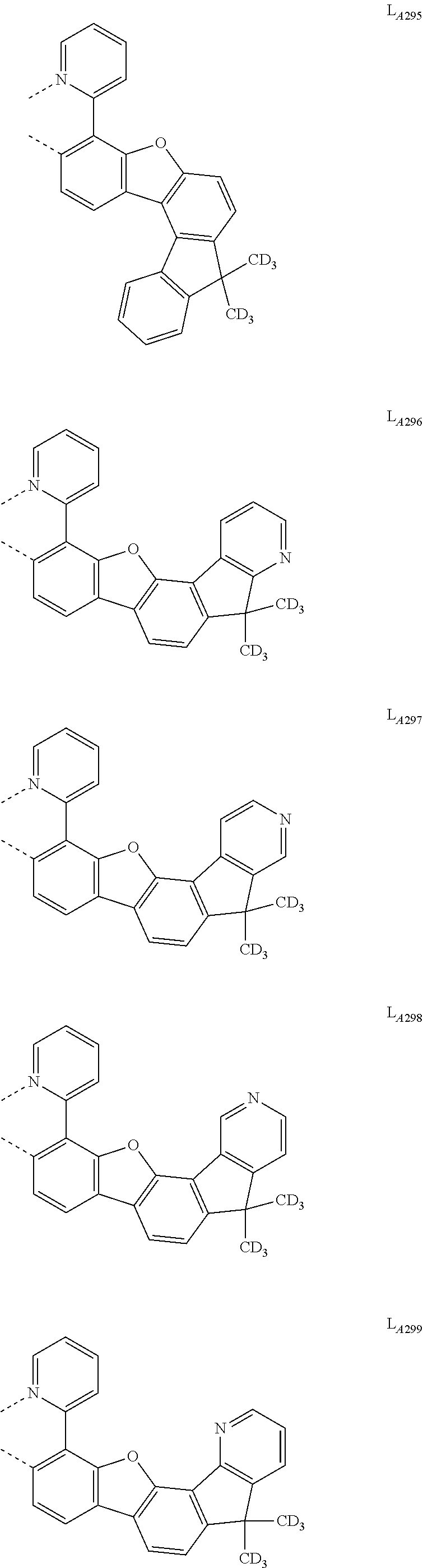


-


-


-


- In one embodiment, the compound of the invention has the formula (LA)Ir(LB)2 of Formula II, having the structure:
-

-
- wherein R7 and R8 each independently represent mono, di, tri, or tetra substitutions, or no substitution;
- wherein R7 and R8 are each independently selected from the group consisting of hydrogen, deuterium, halide, alkyl, cycloalkyl, heteroalkyl, arylalkyl, alkoxy, aryloxy, amino, silyl, alkenyl, cycloalkenyl, heteroalkenyl, alkynyl, aryl, heteroaryl, acyl, carbonyl, carboxylic acids, ester, nitrile, isonitrile, sulfanyl, sulfinyl, sulfonyl, phosphino, and combinations thereof; and wherein any two adjacent R7 and R8 are optionally joined to form a ring, which can be further substituted.
- In one embodiment LB is selected from the group consisting of LB1 to LB225:
-


-


- In one embodiment, the compound is selected from the group consisting of Compound 1 through Compound 114,300; where each compound x has the formula Ir(LAi) (LBj)2, wherein x=508j+i−508, i is an integer from 1 to 508, and j is an integer from 1 to 225; wherein LAi is one of LA1 to LA508 and LB/is one of LB1 to LB225. For example, if the compound has formula Ir(LA35)(LB15)2, the compound is Compound 7,147. In one embodiment, ligand LAi is at least one ligand LA. In one embodiment, ligand LBj is at least one ligand LB.
- In some embodiments, the compound can be an emissive dopant. In some embodiments, the compound can produce emissions via phosphorescence, fluorescence, thermally activated delayed fluorescence, i.e., TADF (also referred to as E-type delayed fluorescence), triplet-triplet annihilation, or combinations of these processes.
- According to another aspect of the present disclosure, an organic light emitting device (OLED) is also provided. The OLED includes an anode, a cathode, and an organic layer disposed between the anode and the cathode. The organic layer may include a host and a phosphorescent dopant. The emissive layer can include a compound according to Formula I, and its variations as described herein.
- The OLED can be one or more of a consumer product, an electronic component module, an organic light-emitting device and a lighting panel. The organic layer can be an emissive layer and the compound can be an emissive dopant in some embodiments, while the compound can be a non-emissive dopant in other embodiments. The organic layer can be a charge transporting layer and the compound can be a charge transporting material in the organic layer in some embodiments. The organic layer can be a blocking layer and the compound can be a blocking material in the organic layer in some embodiments.
- In one embodiment, the OLED is incorporated into a device selected from the group consisting of a consumer product, an electronic component module, and a lighting panel.
- The organic layer can also include a host. In some embodiments, the host can include a metal complex. In one embodiment, the organic layer comprises a host; wherein the host comprises a triphenylene containing benzo-fused thiophene or benzo-fused furan;
-
- wherein any substituent in the host is an unfused substituent independently selected from the group consisting of CnH2n+1, OCnH2n+1, OAr1, N(CnH2n+1)2, N(Ar1)(Ar2), CH═CH—CnH2n+1, C≡CCnH2n+1, Ar1, Ar1—Ar2, CnH2n—Ar1, or no substitution;
- wherein n is from 1 to 10; and
- wherein Ar1 and Ar2 are independently selected from the group consisting of benzene, biphenyl, naphthalene, triphenylene, carbazole, and heteroaromatic analogs thereof.
- In another embodiment, the organic layer further comprises a host, wherein the host comprises at least one chemical group selected from the group consisting of triphenylene, carbazole, dibenzothiphene, dibenzofuran, dibenzoselenophene, azatriphenylene, azacarbazole, aza-dibenzothiophene, aza-dibenzofuran, and aza-dibenzoselenophene. The host can include a metal complex.
- In another embodiment, the organic layer further comprises a host and the host is selected from the group consisting of:
-


- and combinations thereof.
- In one embodiment, the OLED organic layer further comprises a host and the host comprises a metal complex.
-
-
- In yet another aspect of the present disclosure, a formulation that comprises a compound according to Formula I is described. The formulation can include one or more components selected from the group consisting of a solvent, a host, a hole injection material, hole transport material, and an electron transport layer material, disclosed herein.
Combination with Other Materials
- In yet another aspect of the present disclosure, a formulation that comprises a compound according to Formula I is described. The formulation can include one or more components selected from the group consisting of a solvent, a host, a hole injection material, hole transport material, and an electron transport layer material, disclosed herein.
- The materials described herein as useful for a particular layer in an organic light emitting device may be used in combination with a wide variety of other materials present in the device. For example, emissive dopants disclosed herein may be used in conjunction with a wide variety of hosts, transport layers, blocking layers, injection layers, electrodes and other layers that may be present. The materials described or referred to below are non-limiting examples of materials that may be useful in combination with the compounds disclosed herein, and one of skill in the art can readily consult the literature to identify other materials that may be useful in combination.
- A hole injecting/transporting material to be used in the present invention is not particularly limited, and any compound may be used as long as the compound is typically used as a hole injecting/transporting material. Examples of the material include, but are not limited to: a phthalocyanine or porphyrin derivative; an aromatic amine derivative; an indolocarbazole derivative; a polymer containing fluorohydrocarbon; a polymer with conductivity dopants; a conducting polymer, such as PEDOT/PSS; a self-assembly monomer derived from compounds such as phosphonic acid and silane derivatives; a metal oxide derivative, such as MoOx; a p-type semiconducting organic compound, such as 1,4,5,8,9,12-Hexaazatriphenylenehexacarbonitrile; a metal complex, and cross-linkable compounds.
- Examples of aromatic amine derivatives used in HIL or HTL include, but are not limited to the following general structures:
-

- Each of Ar1 to Ar9 is selected from the group consisting of aromatic hydrocarbon cyclic compounds such as benzene, biphenyl, triphenyl, triphenylene, naphthalene, anthracene, phenalene, phenanthrene, fluorene, pyrene, chrysene, perylene, and azulene; the group consisting of aromatic heterocyclic compounds such as dibenzothiophene, dibenzofuran, dibenzoselenophene, furan, thiophene, benzofuran, benzothiophene, benzoselenophene, carbazole, indolocarbazole, pyridylindole, pyrrolodipyridine, pyrazole, imidazole, triazole, oxazole, thiazole, oxadiazole, oxatriazole, dioxazole, thiadiazole, pyridine, pyridazine, pyrimidine, pyrazine, triazine, oxazine, oxathiazine, oxadiazine, indole, benzimidazole, indazole, indoxazine, benzoxazole, benzisoxazole, benzothiazole, quinoline, isoquinoline, cinnoline, quinazoline, quinoxaline, naphthyridine, phthalazine, pteridine, xanthene, acridine, phenazine, phenothiazine, phenoxazine, benzofuropyridine, furodipyridine, benzothienopyridine, thienodipyridine, benzoselenophenopyridine, and selenophenodipyridine; and the group consisting of 2 to 10 cyclic structural units which are groups of the same type or different types selected from the aromatic hydrocarbon cyclic group and the aromatic heterocyclic group and are bonded to each other directly or via at least one of oxygen atom, nitrogen atom, sulfur atom, silicon atom, phosphorus atom, boron atom, chain structural unit and the aliphatic cyclic group. Wherein each Ar is further substituted by a substituent selected from the group consisting of hydrogen, deuterium, halide, alkyl, cycloalkyl, heteroalkyl, arylalkyl, alkoxy, aryloxy, amino, silyl, alkenyl, cycloalkenyl, heteroalkenyl, alkynyl, aryl, heteroaryl, acyl, carbonyl, carboxylic acids, ester, nitrile, isonitrile, sulfanyl, sulfinyl, sulfonyl, phosphino, and combinations thereof.
- In one aspect, Ar1 to Ar9 is independently selected from the group consisting of:
-

- wherein k is an integer from 1 to 20; X101 to X108 is C (including CH) or N; Z101 is NAr1, O, or S; Ar1 has the same group defined above.
- Examples of metal complexes used in HIL or HTL include, but are not limited to the following general formula:
-

- wherein Met is a metal, which can have an atomic weight greater than 40; (Y101-Y102) is a bidentate ligand, Y101 and Y102 are independently selected from C, N, O, P, and S; L101 is an ancillary ligand; k′ is an integer value from 1 to the maximum number of ligands that may be attached to the metal; and k′+k″ is the maximum number of ligands that may be attached to the metal.
- In one aspect, (Y101-Y102) is a 2-phenylpyridine derivative. In another aspect, (Y101-Y102) is a carbene ligand. In another aspect, Met is selected from Ir, Pt, Os, and Zn. In a further aspect, the metal complex has a smallest oxidation potential in solution vs. Fc+/Fc couple less than about 0.6 V.
- The light emitting layer of the organic EL device of the present invention preferably contains at least a metal complex as light emitting material, and may contain a host material using the metal complex as a dopant material. Examples of the host material are not particularly limited, and any metal complexes or organic compounds may be used as long as the triplet energy of the host is larger than that of the dopant. While the Table below categorizes host materials as preferred for devices that emit various colors, any host material may be used with any dopant so long as the triplet criteria is satisfied.
- Examples of metal complexes used as host are preferred to have the following general formula:
-

- wherein Met is a metal; (Y103-Y104) is a bidentate ligand, Y103 and Y104 are independently selected from C, N, O, P, and S; L101 is an another ligand; k′ is an integer value from 1 to the maximum number of ligands that may be attached to the metal; and k′+k″ is the maximum number of ligands that may be attached to the metal.
- In one aspect, the metal complexes are:
-

- wherein (O—N) is a bidentate ligand, having metal coordinated to atoms O and N.
- In another aspect, Met is selected from Ir and Pt. In a further aspect, (Y103-Y104) is a carbene ligand.
- Examples of organic compounds used as host are selected from the group consisting of aromatic hydrocarbon cyclic compounds such as benzene, biphenyl, triphenyl, triphenylene, naphthalene, anthracene, phenalene, phenanthrene, fluorene, pyrene, chrysene, perylene, and azulene; the group consisting of aromatic heterocyclic compounds such as dibenzothiophene, dibenzofuran, dibenzoselenophene, furan, thiophene, benzofuran, benzothiophene, benzoselenophene, carbazole, indolocarbazole, pyridylindole, pyrrolodipyridine, pyrazole, imidazole, triazole, oxazole, thiazole, oxadiazole, oxatriazole, dioxazole, thiadiazole, pyridine, pyridazine, pyrimidine, pyrazine, triazine, oxazine, oxathiazine, oxadiazine, indole, benzimidazole, indazole, indoxazine, benzoxazole, benzisoxazole, benzothiazole, quinoline, isoquinoline, cinnoline, quinazoline, quinoxaline, naphthyridine, phthalazine, pteridine, xanthene, acridine, phenazine, phenothiazine, phenoxazine, benzofuropyridine, furodipyridine, benzothienopyridine, thienodipyridine, benzoselenophenopyridine, and selenophenodipyridine; and the group consisting of 2 to 10 cyclic structural units which are groups of the same type or different types selected from the aromatic hydrocarbon cyclic group and the aromatic heterocyclic group and are bonded to each other directly or via at least one of oxygen atom, nitrogen atom, sulfur atom, silicon atom, phosphorus atom, boron atom, chain structural unit and the aliphatic cyclic group. Wherein each group is further substituted by a substituent selected from the group consisting of hydrogen, deuterium, halide, alkyl, cycloalkyl, heteroalkyl, arylalkyl, alkoxy, aryloxy, amino, silyl, alkenyl, cycloalkenyl, heteroalkenyl, alkynyl, aryl, heteroaryl, acyl, carbonyl, carboxylic acids, ester, nitrile, isonitrile, sulfanyl, sulfinyl, sulfonyl, phosphino, and combinations thereof.
- In one aspect, the host compound contains at least one of the following groups in the molecule:
-


- wherein R101 to R107 is independently selected from the group consisting of hydrogen, deuterium, halide, alkyl, cycloalkyl, heteroalkyl, arylalkyl, alkoxy, aryloxy, amino, silyl, alkenyl, cycloalkenyl, heteroalkenyl, alkynyl, aryl, heteroaryl, acyl, carbonyl, carboxylic acids, ester, nitrile, isonitrile, sulfanyl, sulfinyl, sulfonyl, phosphino, and combinations thereof, when it is aryl or heteroaryl, it has the similar definition as Ar's mentioned above. k is an integer from 0 to 20 or 1 to 20; k′″ is an integer from 0 to 20. X101 to X108 is selected from C (including CH) or N. Z101 and Z102 is selected from NR101, O, or S.
- A hole blocking layer (HBL) may be used to reduce the number of holes and/or excitons that leave the emissive layer. The presence of such a blocking layer in a device may result in substantially higher efficiencies as compared to a similar device lacking a blocking layer. Also, a blocking layer may be used to confine emission to a desired region of an OLED.
- In one aspect, the compound used in the HBL contains the same molecule or the same functional groups used as the host described above.
- In another aspect, the compound used in the HBL contains at least one of the following groups in the molecule:
-

- wherein k is an integer from 1 to 20; L101 is an another ligand, k′ is an integer from 1 to 3.
- Electron transport layer (ETL) may include a material capable of transporting electrons. Electron transport layer may be intrinsic (undoped), or doped. Doping may be used to enhance conductivity. Examples of the ETL material are not particularly limited, and any metal complexes or organic compounds may be used as long as they are typically used to transport electrons.
- In one aspect, the compound used in ETL contains at least one of the following groups in the molecule:
-

- wherein R101 is selected from the group consisting of hydrogen, deuterium, halide, alkyl, cycloalkyl, heteroalkyl, arylalkyl, alkoxy, aryloxy, amino, silyl, alkenyl, cycloalkenyl, heteroalkenyl, alkynyl, aryl, heteroaryl, acyl, carbonyl, carboxylic acids, ester, nitrile, isonitrile, sulfanyl, sulfinyl, sulfonyl, phosphino, and combinations thereof, when it is aryl or heteroaryl, it has the similar definition as Ar's mentioned above. Ar1 to Ar3 has the similar definition as Ar's mentioned above. k is an integer from 1 to 20. X101 to X108 is selected from C (including CH) or N.
- In another aspect, the metal complexes used in ETL contains, but is not limited to, the following general formula:
-

- wherein (O—N) or (N—N) is a bidentate ligand, having metal coordinated to atoms O, N or N, N; L101 is another ligand; k′ is an integer value from 1 to the maximum number of ligands that may be attached to the metal.
- In any above-mentioned compounds used in each layer of the OLED device, the hydrogen atoms can be partially or fully deuterated. Thus, any specifically listed substituent, such as, without limitation, methyl, phenyl, pyridyl, etc. encompasses undeuterated, partially deuterated, and fully deuterated versions thereof. Similarly, classes of substituents such as, without limitation, alkyl, aryl, cycloalkyl, heteroaryl, etc. also encompass undeuterated, partially deuterated, and fully deuterated versions thereof.
- In addition to and/or in combination with the materials disclosed herein, many hole injection materials, hole transporting materials, host materials, dopant materials, exiton/hole blocking layer materials, electron transporting and electron injecting materials may be used in an OLED. Non-limiting examples of the materials that may be used in an OLED in combination with materials disclosed herein are listed in Table A below. Table A lists non-limiting classes of materials, non-limiting examples of compounds for each class, and references that disclose the materials.
-
TABLE A MATERIAL EXAMPLES OF MATERIAL PUBLICATIONS Hole injection materials Phthalocyanine and porphyrin compounds 
Appl. Phys. Lett. 69, 2160 (1996) Starburst triarylamines 
J. Lumin. 72-74, 985 (1997) CFx Fluorohydrocarbon polymer 
Appl. Phys. Lett. 78, 673 (2001) Conducting polymers (e.g., PEDOT:PSS, polyaniline, polythiophene 
Synth. Met. 87, 171 (1997) WO2007002683 Phosphonic acid and silane SAMs 
US20030162053 Triarylamine or polythiophene polymers with conductivity dopants 
EP1725079A1 

Organic compounds with conductive inorganic compounds, such as molybdenum and tungsten oxides 
US20050123751 SID Symposium Digest, 37, 923 (2006) WO2009018009 n-type semiconducting organic complexes 
US20020158242 Metal organometallic complexes 
US20060240279 Cross-linkable compounds 
US20080220265 Polythiophene based polymers and copolymers 
WO2011075644 EP2350216 Hole transporting materials Triarylamines (e.g., TPD, α-NPD) 
Appl. Phys. Lett. 51, 913 (1987) 
U.S. Pat. No. 5,061,569 
EP650955 
J. Mater. Chem. 3, 319 (1993) 
Appl. Phys. Lett. 90, 183503 (2007) 
Appl. Phys. Lett. 90, 183503 (2007) Triarylamine on spirofluorene core 
Synth. Met. 91, 209 (1997) Arylamine carbazole compounds 
Adv. Mater. 6, 677 (1994), US20080124572 Triarylamine with (di)benzothiophene/ (di)benzofuran 
US20070278938, US20080106190 US20110163302 Indolocarbazoles 
Synth. Met. 111, 421 (2000) Isoindole compounds 
Chem. Mater. 15, 3148 (2003) Metal carbene complexes 
US20080018221 Phosphorescent OLED host materials Red hosts Arylcarbazoles 
Appl. Phys. Lett. 78, 1622 (2001) Metal 8-hydroxyquinolates (e.g., Alq3, BAlq) 
Nature 395, 151 (1998) 
US20060202194 
WO2005014551 
WO2006072002 Metal phenoxybenzothiazole compounds 
Appl. Phys. Lett. 90, 123509 (2007) Conjugated oligomers and polymers (e.g., polyfluorene) 
Org. Electron. 1, 15 (2000) Aromatic fused rings 
WO2009066779, WO2009066778, WO2009063833, US20090045731, US20090045730, WO2009008311, US20090008605, US20090009065 Zinc complexes 
WO2010056066 Chrysene based compounds 
WO2011086863 Green hosts Arylcarbazoles 
Appl. Phys. Lett. 78, 1622 (2001) 
US20030175553 
WO2001039234 Aryltriphenylene compounds 
US20060280965 
US20060280965 
WO2009021126 Poly-fused heteroaryl compounds 
US20090309488 US20090302743 US20100012931 Donor acceptor type molecules 
WO2008056746 
WO2010107244 Aza-carbazole/ DBT/DBF 
JP2008074939 
US20100187984 Polymers (e.g., PVK) 
Appl. Phys. Lett. 77, 2280 (2000) Spirofluorene compounds 
WO2004093207 Metal phenoxybenzooxazole compounds 
WO2005089025 
WO2006132173 
JP200511610 Spirofluorene- carbazole compounds 
JP2007254297 
JP2007254297 Indolocarbazoles 
WO2007063796 
WO2007063754 5-member ring electron deficient heterocycles (e.g., triazole, oxadiazole) 
J. Appl. Phys. 90, 5048 (2001) 
WO2004107822 Tetraphenylene complexes 
US20050112407 Metal phenoxypyridine compounds 
WO2005030900 Metal coordination complexes (e.g., Zn, Al with N{circumflex over ( )}N ligands) 
US20040137268, US20040137267 Blue hosts Arylcarbazoles 
Appl. Phys. Lett, 82, 2422 (2003) 
US20070190359 Dibenzothiophene/ Dibenzofuran- carbazole compounds 
WO2006114966, US20090167162 
US20090167162 
WO2009086028 
US20090030202, US20090017330 
US20100084966 Silicon aryl compounds 
US20050238919 
WO2009003898 Silicon/Germanium aryl compounds 
EP2034538A Aryl benzoyl ester 
WO2006100298 Carbazole linked by non-conjugated groups 
US20040115476 Aza-carbazoles 
US20060121308 High triplet metal organometallic complex 
U.S. Pat. No. 7,154,114 Phosphorescent dopants Red dopants Heavy metal porphyrins (e.g., PtOEP) 
Nature 395, 151 (1998) Iridium (III) organometallic complexes 
Appl. Phys. Lett. 78, 1622 (2001) 
US20030072964 
US20030072964 
US20060202194 
US20060202194 
US20070087321 
US20080261076 US20100090591 
US20070087321 
Adv. Mater. 19, 739 (2007) 
WO2009100991 
WO2008101842 
U.S. Pat. No. 7,232,618 Platinum (II) organometallic complexes 
WO2003040257 
US20070103060 Osmium (III) complexes 
Chem. Mater. 17, 3532 (2005) Ruthenium (II) complexes 
Adv. Mater. 17, 1059 (2005) Rhenium (I), (II), and (III) complexes 
US20050244673 Green dopants Iridium (III) organometallic complexes 
Inorg. Chem. 40, 1704 (2001) 
US20020034656 
U.S. Pat. No. 7,332,232 
US20090108737 
WO2010028151 
EP1841834B 
US20060127696 
US20090039776 
U.S. Pat. No. 6,921,915 
US20100244004 
U.S. Pat. No. 6,687,266 
Chem. Mater. 16, 2480 (2004) 
US20070190359 
US20060008670 JP2007123392 
WO2010086089, WO2011044988 
Adv. Mater. 16, 2003 (2004) 
Angew. Chem. Int. Ed. 2006, 45, 7800 
WO2009050290 
US20090165846 
US20080015355 
US20010015432 
US20100295032 Monomer for polymeric metal organometallic compounds 
U.S. Pat. No. 7,250,226, U.S. Pat. No. 7,396,598 Pt (II) organometallic complexes, including polydentated ligands 
Appl. Phys. Lett. 86, 153505 (2005) 
Appl. Phys. Lett. 86, 153505 (2005) 
Chem. Lett. 34, 592 (2005) 
WO2002015645 
US20060263635 
US20060182992 US20070103060 Cu complexes 
WO2009000673 
US20070111026 Gold complexes 
Chem. Commun. 2906 (2005) Rhenium (III) complexes 
Inorg. Chem. 42, 1248 (2003) Osmium (II) complexes 
U.S. Pat. No. 7,279,704 Deuterated organometallic complexes 
US20030138657 Organometallic complexes with two or more metal centers 
US20030152802 
U.S. Pat. No. 7,090,928 Blue dopants Iridium (III) organometallic complexes 
WO2002002714 
WO2006009024 
US20060251923 US20110057559 US20110204333 
U.S. Pat. No. 7,393,599, WO2006056418, US20050260441, WO2005019373 
U.S. Pat. No. 7,534,505 
WO2011051404 
U.S. Pat. No. 7,445,855 
US20070190359, US20080297033 US20100148663 
U.S. Pat. No. 7,338,722 
US20020134984 
Angew. Chem. Int. Ed. 47, 4542 (2008) 
Chem. Mater. 18, 5119 (2006) 
Inorg. Chem. 46, 4308 (2007) 
WO2005123873 
WO2005123873 
WO2007004380 
WO2006082742 Osmium (II) complexes 
U.S. Pat. No. 7,279,704 
Organometallics 23, 3745 (2004) Gold complexes 
Appl. Phys. Lett. 74, 1361 (1999) Platinum (II) complexes 
WO2006098120, WO2006103874 Pt tetradentate complexes with at least one metal- carbene bond 
U.S. Pat. No. 7,655,323 Exciton/hole blocking layer materials Bathocuprine compounds (e.g., BCP, BPhen) 
Appl. Phys. Lett. 75, 4 (1999) 
Appl. Phys. Lett. 79, 449 (2001) Metal 8-hydroxyquinolates (e.g., BAlq) 
Appl. Phys. Lett. 81, 162 (2002) 5-member ring electron deficient heterocycles such as triazole, oxadiazole, imidazole, benzoimidazole 
Appl. Phys. Lett. 81, 162 (2002) Triphenylene compounds 
US20050025993 Fluorinated aromatic compounds 
Appl. Phys. Lett. 79, 156 (2001) Phenothiazine-S-oxide 
WO2008132085 Silylated five-membered nitrogen, oxygen, sulfur or phosphorus dibenzoheterocycles 
WO2010079051 Aza-carbazoles 
US20060121308 Electron transporting materials Anthracene- benzoimidazole compounds 
WO2003060956 
US20090179554 Aza triphenylene derivatives 
US20090115316 Anthracene- benzothiazole compounds 
Appl. Phys. Lett. 89, 063504 (2006) Metal 8-hydroxyquinolates (e.g., Alq3, Zrq4) 
Appl. Phys. Lett. 51, 913 (1987) U.S. Pat. No. 7,230,107 Metal hydroxybenzoquinolates 
Chem. Lett. 5, 905 (1993) Bathocuprine compounds such as BCP, BPhen, etc. 
Appl. Phys. Lett. 91, 263503 (2007) 
Appl. Phys. Lett. 79, 449 (2001) 5-member ring electron deficient heterocycles (e.g..triazole, oxadiazole, imidazole, benzoimidazole) 
Appl. Phys. Lett. 74, 865 (1999) 
Appl. Phys. Lett. 55, 1489 (1989) 
Jpn. J. Apply. Phys. 32, L917 (1993) Silole compounds 
Org. Electron. 4, 113 (2003) Arylborane compounds 
J. Am. Chem. Soc. 120, 9714 (1998) Fluorinated aromatic compounds 
J. Am. Chem. Soc. 122, 1832 (2000) Fullerene (e.g., C60) 
US20090101870 Triazine complexes 
US20040036077 Zn (N{circumflex over ( )}N) complexes 
U.S. Pat. No. 6,528,187 - All example devices were fabricated by high vacuum (<10−7 Torr) thermal evaporation. The anode electrode is 800 Å of indium tin oxide (ITO). The cathode consisted of 10 Å of LiF followed by 1,000 Å of Al. All devices are encapsulated with a glass lid sealed with an epoxy resin in a nitrogen glove box (<1 ppm of H2O and O2) immediately after fabrication, and a moisture getter was incorporated inside the package. The organic stack of the device examples consisted of sequentially, from the ITO surface, 100 Å of LG101 as the hole injection layer (HIL), 450 Å of Compound D as the hole transporting layer (HTL), 400 Å of Compound 1 doped in Compound B as host with 10 or 15 weight percent of the iridium phosphorescent compound as the emissive layer (EML), 50 Å of Compound C as a blocking layer (BL), 450 Å of Alq (tris-8-hydroxyquinoline aluminum) as the ETL. The comparative Example with Compound A was fabricated similarly to the Device Examples. The device results and data are summarized in Tables 1 and 2. As used herein, Alq, Compound A, B, C and D have the following structures:
-


-
TABLE 1 Device Structures of Inventive Compound and Comparative Compound EML (400 Å, Example HIL HTL doping %) BL ETL Comparative LG101 Com- Com- Com- Com- Alq Example 1 100 Å pound D pound pound A pound C 450 Å 450 Å B as host 10% 50 Å Comparative LG101 Com- Com- Com- Com- Alq Example 2 100 Å pound D pound pound A pound C 450 Å 450 Å B as host 15% 50 Å Inventive LG101 Com- Com- Com- Com- Alq Example 1 100 Å pound D pound pound 1 pound C 450 Å 450 Å B as host 10% 50 Å Inventive LG101 Com- Com- Com- Com- Alq Example 2 100 Å pound D pound pound 1 pound C 450 Å 450 Å B as host 15% 50 Å -
TABLE 2 VTE Device Results LT95% (h) λmax FWHM At 40 x y (nm) (nm) mA/cm2 Comparative example 1 0.335 0.633 528 58 18 Comparative example 2 0.340 0.630 530 59 9 Inventive example 1 0.344 0.626 530 58 32 Inventive example 2 0.347 0.626 530 58 24 - Table 2 is the summary of EL of comparative and inventive devices at 1000 nits and life test at 40 mA/cm2. The LT 95% of Comparative example Compound A at dopant concentration 10% and 15% are 18 and 9 hours vs 32 and 24 hours for inventive example Compound 1, respectively. The device lifetime results demonstrated that a fused ring and rigidification of molecules can result in better device performance in term of lifetime, which is a desired property for OLED devices.
-

- To a 500 mL round bottom flask, methyl-2-bromobenzoate (15 g, 69.8 mmol), dibenzo[b,d]furan-4-ylboronic acid (16.27 g, 77 mmol), Pd(PPh3)4 (0.806 g, 0.698 mmol), K2CO3 (19.28
g 140 mmol) and 250 mL THF were added and nitrogen was bubbled through the reaction mixture for 30 mins. The reaction mixture was heated up to reflux and stirred at reflux overnight. The reaction mixture was cooled down and purified using a silica gel column with DCM 50% in heptane as elutant and about 8 grams (38% yield) of pure product was obtained. -

- Methyl 2-(dibenzo[b,d]furan-4-yl)benzoate (7.7 g, 25.5 mmol) was dissolved in ˜150 mL anhydrous THF and cooled down to 0° C. To the solution, ˜25.5 mL of a 3 M methyl magnesium bromide diether solution was added slowly and the reaction mixture was stirred overnight. The reaction mixture was quenched with NH4Cl aqueous solution and extracted with DCM and dried over Na2SO4. ˜8 gram product was obtained after evaporation of DCM. The product, which was confirmed by GC, was used for the next step without further purification.
-

- 2-(2-dibenzo[b,d]furan-4-yl)phenylpropan-2-ol (8.0 g, 26.5 mmol) was dissolved in 150 mL DCM and cooled down to 0° C. . . . To the solution, 10 mL of a BF3 (46.5%) ether complex solution was added slowly, then the reaction mixture was stirred overnight. Saturated NaHCO3 aqueous solution was slowly added while stirring until the formation of bubbles stopped. The reaction mixture was purified using a silica column with 15% DCM in heptane as eluant. ˜4 g product was obtained after column. The product was confirmed by proton NMR and GC.
-

- 7,7-dimethyl-7H-fluoreno[4,3-b]benzofuran (4.0 g, 14.07 mmol) was dissolved in anhydrous THF and cooled down to −78° C. 30 mL of 1.4 M Sec-BuLi in cyclohexane was added into the solution once, and the reaction mixture was stirred for two hours at −78° C. ˜11.5 mL 2-isopropoxy-4,4,5,5-tetramethyl-1,3,2-dioxaborolane was added and the reaction mixture was stirred overnight. The reaction mixture was quenched with NH4OH aqueous solution and purified using a silica gel column to yield ˜2.1 g (36.5% yield) product.
-

- A round flask was charged with 2-(7,7-dimethyl-7H-fluoreno[4,3-b]benzofuran-1-yl)-4,4,5,5-tetramethyl-1,3,2-dioxaborolane (2.0 g, 4.87 mmol), 2-chloropyridine (0.664 g, 5.85 mmol), Pd2(dba)3 (0.09 g, 0.098 mmol), dicyclohexyl(2′,6′-dimethoxy-[1,1′-biphenyl]-2-yl)phosphine (0.16 g, 0.39 mmol), K3PO4 (3.62 g, 17.06 mmol), 150 mL toluene and 15 mL water. Nitrogen was bubbled through the reaction mixture for 20 mins, and then the reaction mixture was heated up to reflux and stirred at reflux overnight. The product was purified using silica gel chromatograph, and was confirmed by GC. ˜1.3 g product (73.8% yield) was obtained.
-

- A round flask was charged with iridium complex precursor (1.6 g, 2.24 mmol), 2-(7,7-dimethyl-7H-fluoreno[4,3-b]benzofuran-1-yl)pyridine (1.3 g, 3.59 mmol), 30 mL methanol and 30 mL ethanol. The reaction mixture was heated up to reflux (oil bath; ˜85° C.) for and stirred at reflux for 7 days. The reaction mixture was purified using a silica gel column. ˜0.82 g (42.5% yield) pure product was isolated, which was confirmed by LC-MS and HPLC.
- It is understood that the various embodiments described herein are by way of example only, and are not intended to limit the scope of the invention. For example, many of the materials and structures described herein may be substituted with other materials and structures without deviating from the spirit of the invention. The present invention as claimed may therefore include variations from the particular examples and preferred embodiments described herein, as will be apparent to one of skill in the art. It is understood that various theories as to why the invention works are not intended to be limiting.
- The disclosures of each and every patent, patent application, and publication cited herein are hereby incorporated herein by reference in their entirety. While this invention has been disclosed with reference to specific embodiments, it is apparent that other embodiments and variations of this invention may be devised by others skilled in the art without departing from the true spirit and scope of the invention. The appended claims are intended to be construed to include all such embodiments and equivalent variations.
Claims (21)
1.-23. (canceled)
24. A compound comprising a ligand LA of Formula I:

wherein R has the following structure and is fused to ring A:

wherein each Z1 to Z8 is nitrogen or carbon;
wherein the wave lines indicate the bonds to two of the adjacent Z1 to Z4 of ring A;
wherein when two of the adjacent Z1 to Z4 are used to fuse to R, those two of the adjacent Z1 to Z4 are carbon;
wherein R1 and R4 each independently represent mono, di, tri, or tetra substitutions, or no substitution;
wherein R2 and R3 each independently represent mono, or di substitutions, or no substitution;
wherein X is O or S;
each R1 is independently selected from the group consisting of hydrogen, deuterium, halide, alkyl, cycloalkyl, heteroalkyl, arylalkyl, alkoxy, aryloxy, amino, silyl, alkenyl, cycloalkenyl, heteroalkenyl, alkynyl, aryl, heteroaryl, acyl, carbonyl, carboxylic acids, ester, nitrile, isonitrile, sulfanyl, sulfinyl, sulfonyl, phosphino, and combinations thereof;
each R2 is independently selected from the group consisting of hydrogen, deuterium, halide, alkyl, cycloalkyl, heteroalkyl, arylalkyl, alkoxy, aryloxy, amino, silyl, alkenyl, cycloalkenyl, heteroalkenyl, alkynyl, aryl, heteroaryl, acyl, carbonyl, carboxylic acids, ester, nitrile, isonitrile, sulfanyl, sulfinyl, sulfonyl, phosphino, and combinations thereof;
each R3 is independently selected from the group consisting of hydrogen, deuterium, halide, alkyl, cycloalkyl, heteroalkyl, arylalkyl, alkoxy, aryloxy, amino, silyl, alkenyl, cycloalkenyl, heteroalkenyl, alkynyl, aryl, heteroaryl, acyl, carbonyl, carboxylic acids, ester, nitrile, isonitrile, sulfanyl, sulfinyl, sulfonyl, phosphino, and combinations thereof;
each R4 is independently selected from the group consisting of hydrogen, deuterium, halide, alkyl, cycloalkyl, heteroalkyl, arylalkyl, alkoxy, aryloxy, amino, silyl, alkenyl, cycloalkenyl, heteroalkenyl, alkynyl, aryl, heteroaryl, acyl, carbonyl, carboxylic acids, ester, nitrile, isonitrile, sulfanyl, sulfinyl, sulfonyl, phosphino, and combinations thereof;
R5 is selected from the group consisting of hydrogen, deuterium, halide, alkyl, cycloalkyl, heteroalkyl, arylalkyl, alkoxy, aryloxy, amino, silyl, alkenyl, cycloalkenyl, heteroalkenyl, alkynyl, aryl, heteroaryl, acyl, carbonyl, carboxylic acids, ester, nitrile, isonitrile, sulfanyl, sulfinyl, sulfonyl, phosphino, and combinations thereof;
R6 is selected from the group consisting of hydrogen, deuterium, halide, alkyl, cycloalkyl, heteroalkyl, arylalkyl, alkoxy, aryloxy, amino, silyl, alkenyl, cycloalkenyl, heteroalkenyl, alkynyl, aryl, heteroaryl, acyl, carbonyl, carboxylic acids, ester, nitrile, isonitrile, sulfanyl, sulfinyl, sulfonyl, phosphino, and combinations thereof,
wherein any two adjacent substituents are optionally joined to form a ring, which can be further substituted;
wherein the ligand LA is coordinated to a metal M;
wherein the ligand LA is optionally linked with other ligands to comprise a tridentate, tetradentate, pentadentate or hexadentate ligand; and
wherein at least one of R1, R2, R3, R4, R5, and R6 is not hydrogen or deuterium.
25. The compound of claim 24 , wherein M is selected from the group consisting of Ir, Rh, Re, Ru, Os, Pt, Au, and Cu.
26. The compound of claim 24 , wherein at least one of Z1, Z2, Z3, and Z4 is nitrogen or at least one of Z5 and Z6 is nitrogen.
27. The compound of claim 24 , wherein each R1 is independently selected from the group consisting of hydrogen, deuterium, halide, alkyl, cycloalkyl, alkoxy, aryloxy, amino, silyl, alkenyl, aryl, heteroaryl, nitrile, and combinations thereof.
28. The compound of claim 24 , wherein each R1 is independently selected from the group consisting of hydrogen, deuterium, halide, alkyl, cycloalkyl, silyl, aryl, heteroaryl, nitrile, and combinations thereof.
29. The compound of claim 24 , wherein each R2 is independently selected from the group consisting of hydrogen, deuterium, halide, alkyl, cycloalkyl, alkoxy, aryloxy, amino, silyl, alkenyl, aryl, heteroaryl, nitrile, and combinations thereof.
30. The compound of claim 24 , wherein each R3 is independently selected from the group consisting of hydrogen, deuterium, halide, alkyl, cycloalkyl, alkoxy, aryloxy, amino, silyl, alkenyl, aryl, heteroaryl, nitrile, and combinations thereof.
31. The compound of claim 24 , wherein each R3 is independently selected from the group consisting of hydrogen, deuterium, halide, alkyl, cycloalkyl, silyl, aryl, heteroaryl, nitrile, and combinations thereof.
32. The compound of claim 24 , wherein each R4 is independently selected from the group consisting of hydrogen, deuterium, halide, alkyl, cycloalkyl, alkoxy, aryloxy, amino, silyl, alkenyl, aryl, heteroaryl, nitrile, and combinations thereof.
33. The compound of claim 24 , wherein each R4 is independently selected from the group consisting of hydrogen, deuterium, halide, alkyl, cycloalkyl, silyl, aryl, heteroaryl, nitrile, and combinations thereof.
34. The compound of claim 24 , wherein each R5 and R6 are independently selected from the group consisting of alkyl, cycloalkyl, heteroalkyl, arylalkyl, alkoxy, aryloxy, amino, silyl, alkenyl, cycloalkenyl, heteroalkenyl, alkynyl, aryl, heteroaryl, acyl, carbonyl, carboxylic acids, ester, nitrile, isonitrile, sulfanyl, sulfinyl, sulfonyl, phosphino, and combinations thereof.
35. The compound of claim 33 , wherein R5 and R6 join to form a ring, which is optionally further substituted.
36. The compound of claim 24 , wherein at least one of R1, R2, R3, R4, R5, and R6 is selected from the group consisting of deuterium, halide, alkyl, cycloalkyl, heteroalkyl, arylalkyl, alkoxy, aryloxy, amino, silyl, alkenyl, cycloalkenyl, heteroalkenyl, alkynyl, aryl, heteroaryl, acyl, carbonyl, carboxylic acids, ester, nitrile, isonitrile, sulfanyl, sulfinyl, sulfonyl, phosphino, partially deuterated versions thereof, fully deuterated versions thereof, and combinations thereof.
37. The compound of claim 35 , wherein at least one of R1, R2, R3, R4, R5, and R6 is selected from the group consisting of halide, alkyl, cycloalkyl, silyl, alkenyl, aryl, heteroaryl, nitrile, partially deuterated versions thereof, and fully deuterated versions thereof, and combinations thereof.
38. The compound of claim 24 , wherein the ligand LA is selected from the group consisting of:


39. The compound of claim 24 , wherein the ligand LA is selected from the group consisting of:


40. The compound of claim 24 , wherein the ligand LA is selected from the group consisting of:


41. The compound of claim 24 , wherein the compound is selected from the group consisting of Compound 1 through Compound 114,300;
where each Compound x has the formula Ir(LAi) (LBj)2;
wherein x=508j+i−508, i is an integer from 1 to 508, and j is an integer from 1 to 225;
wherein LBj has the following formula:


42. An organic light emitting device (OLED) comprising:
an anode;
a cathode; and
an organic layer, disposed between the anode and the cathode, comprising a compound comprising a ligand LA of Formula I:

wherein R has the following structure and is fused to ring A:

wherein each Z1 to Z8 is nitrogen or carbon;
wherein the wave lines indicate the bonds to two of the adjacent Z1 to Z4 of ring A;
wherein when two of the adjacent Z1 to Z4 are used to fuse to R, those two of the adjacent Z1 to Z4 are carbon;
wherein R1 and R4 each independently represent mono, di, tri, or tetra substitutions, or no substitution;
wherein R2 and R3 each independently represent mono, or di substitutions, or no substitution;
wherein X is O or S;
each R1 is independently selected from the group consisting of hydrogen, deuterium, halide, alkyl, cycloalkyl, heteroalkyl, arylalkyl, alkoxy, aryloxy, amino, silyl, alkenyl, cycloalkenyl, heteroalkenyl, alkynyl, aryl, heteroaryl, acyl, carbonyl, carboxylic acids, ester, nitrile, isonitrile, sulfanyl, sulfinyl, sulfonyl, phosphino, and combinations thereof;
each R2 is independently selected from the group consisting of hydrogen, deuterium, halide, alkyl, cycloalkyl, heteroalkyl, arylalkyl, alkoxy, aryloxy, amino, silyl, alkenyl, cycloalkenyl, heteroalkenyl, alkynyl, aryl, heteroaryl, acyl, carbonyl, carboxylic acids, ester, nitrile, isonitrile, sulfanyl, sulfinyl, sulfonyl, phosphino, and combinations thereof;
each R3 is independently selected from the group consisting of hydrogen, deuterium, halide, alkyl, cycloalkyl, heteroalkyl, arylalkyl, alkoxy, aryloxy, amino, silyl, alkenyl, cycloalkenyl, heteroalkenyl, alkynyl, aryl, heteroaryl, acyl, carbonyl, carboxylic acids, ester, nitrile, isonitrile, sulfanyl, sulfinyl, sulfonyl, phosphino, and combinations thereof;
each R4 is independently selected from the group consisting of hydrogen, deuterium, halide, alkyl, cycloalkyl, heteroalkyl, arylalkyl, alkoxy, aryloxy, amino, silyl, alkenyl, cycloalkenyl, heteroalkenyl, alkynyl, aryl, heteroaryl, acyl, carbonyl, carboxylic acids, ester, nitrile, isonitrile, sulfanyl, sulfinyl, sulfonyl, phosphino, and combinations thereof;
R5 is selected from the group consisting of hydrogen, deuterium, halide, alkyl, cycloalkyl, heteroalkyl, arylalkyl, alkoxy, aryloxy, amino, silyl, alkenyl, cycloalkenyl, heteroalkenyl, alkynyl, aryl, heteroaryl, acyl, carbonyl, carboxylic acids, ester, nitrile, isonitrile, sulfanyl, sulfinyl, sulfonyl, phosphino, and combinations thereof;
R6 is selected from the group consisting of hydrogen, deuterium, halide, alkyl, cycloalkyl, heteroalkyl, arylalkyl, alkoxy, aryloxy, amino, silyl, alkenyl, cycloalkenyl, heteroalkenyl, alkynyl, aryl, heteroaryl, acyl, carbonyl, carboxylic acids, ester, nitrile, isonitrile, sulfanyl, sulfinyl, sulfonyl, phosphino, and combinations thereof;
wherein any two adjacent substituents are optionally joined to form a ring, which can be further substituted;
wherein the ligand LA is coordinated to a metal M; and
wherein the ligand LA is optionally linked with other ligands to comprise a tridentate, tetradentate, pentadentate or hexadentate ligand; and
wherein at least one of R1, R2, R3, R4, R5, and R6 is not hydrogen or deuterium.
43. A formulation comprising a compound comprising a ligand LA of Formula I:

wherein R has the following structure and is fused to ring A:

wherein each Z1 to Z8 is nitrogen or carbon;
wherein the wave lines indicate the bonds to two of the adjacent Z1 to Z4 of ring A;
wherein when two of the adjacent Z1 to Z4 are used to fuse to R, those two of the adjacent Z1 to Z4 are carbon;
wherein R1 and R4 each independently represent mono, di, tri, or tetra substitutions, or no substitution;
wherein R2 and R3 each independently represent mono, or di substitutions, or no substitution;
each R1 is independently selected from the group consisting of hydrogen, deuterium, halide, alkyl, cycloalkyl, heteroalkyl, arylalkyl, alkoxy, aryloxy, amino, silyl, alkenyl, cycloalkenyl, heteroalkenyl, alkynyl, aryl, heteroaryl, acyl, carbonyl, carboxylic acids, ester, nitrile, isonitrile, sulfanyl, sulfinyl, sulfonyl, phosphino, and combinations thereof;
each R2 is independently selected from the group consisting of hydrogen, deuterium, halide, alkyl, cycloalkyl, heteroalkyl, arylalkyl, alkoxy, aryloxy, amino, silyl, alkenyl, cycloalkenyl, heteroalkenyl, alkynyl, aryl, heteroaryl, acyl, carbonyl, carboxylic acids, ester, nitrile, isonitrile, sulfanyl, sulfinyl, sulfonyl, phosphino, and combinations thereof;
each R3 is independently selected from the group consisting of hydrogen, deuterium, halide, alkyl, cycloalkyl, heteroalkyl, arylalkyl, alkoxy, aryloxy, amino, silyl, alkenyl, cycloalkenyl, heteroalkenyl, alkynyl, aryl, heteroaryl, acyl, carbonyl, carboxylic acids, ester, nitrile, isonitrile, sulfanyl, sulfinyl, sulfonyl, phosphino, and combinations thereof;
each R4 is independently selected from the group consisting of hydrogen, deuterium, halide, alkyl, cycloalkyl, heteroalkyl, arylalkyl, alkoxy, aryloxy, amino, silyl, alkenyl, cycloalkenyl, heteroalkenyl, alkynyl, aryl, heteroaryl, acyl, carbonyl, carboxylic acids, ester, nitrile, isonitrile, sulfanyl, sulfinyl, sulfonyl, phosphino, and combinations thereof;
R5 is selected from the group consisting of hydrogen, deuterium, halide, alkyl, cycloalkyl, heteroalkyl, arylalkyl, alkoxy, aryloxy, amino, silyl, alkenyl, cycloalkenyl, heteroalkenyl, alkynyl, aryl, heteroaryl, acyl, carbonyl, carboxylic acids, ester, nitrile, isonitrile, sulfanyl, sulfinyl, sulfonyl, phosphino, and combinations thereof;
R6 is selected from the group consisting of hydrogen, deuterium, halide, alkyl, cycloalkyl, heteroalkyl, arylalkyl, alkoxy, aryloxy, amino, silyl, alkenyl, cycloalkenyl, heteroalkenyl, alkynyl, aryl, heteroaryl, acyl, carbonyl, carboxylic acids, ester, nitrile, isonitrile, sulfanyl, sulfinyl, sulfonyl, phosphino, and combinations thereof,
wherein any two adjacent substituents are optionally joined to form a ring, which can be further substituted;
wherein the ligand LA is coordinated to a metal M;
wherein the ligand LA is optionally linked with other ligands to comprise a tridentate, tetradentate, pentadentate or hexadentate ligand; and
wherein at least one of R1, R2, R3, R4, R5, and R6 is not hydrogen or deuterium.
Priority Applications (1)
| Application Number | Priority Date | Filing Date | Title |
|---|---|---|---|
| US18/982,362 US20250183166A1 (en) | 2014-11-10 | 2024-12-16 | Organic Electroluminescent Materials and Devices |
Applications Claiming Priority (4)
| Application Number | Priority Date | Filing Date | Title |
|---|---|---|---|
| US201462077469P | 2014-11-10 | 2014-11-10 | |
| US14/887,955 US10868261B2 (en) | 2014-11-10 | 2015-10-20 | Organic electroluminescent materials and devices |
| US17/104,078 US11574867B2 (en) | 2020-11-25 | 2020-11-25 | Non-planar silicided semiconductor electrical fuse |
| US18/982,362 US20250183166A1 (en) | 2014-11-10 | 2024-12-16 | Organic Electroluminescent Materials and Devices |
Related Parent Applications (1)
| Application Number | Title | Priority Date | Filing Date |
|---|---|---|---|
| US17/104,078 Continuation US11574867B2 (en) | 2014-11-10 | 2020-11-25 | Non-planar silicided semiconductor electrical fuse |
Publications (1)
| Publication Number | Publication Date |
|---|---|
| US20250183166A1 true US20250183166A1 (en) | 2025-06-05 |
Family
ID=95859909
Family Applications (1)
| Application Number | Title | Priority Date | Filing Date |
|---|---|---|---|
| US18/982,362 Pending US20250183166A1 (en) | 2014-11-10 | 2024-12-16 | Organic Electroluminescent Materials and Devices |
Country Status (1)
| Country | Link |
|---|---|
| US (1) | US20250183166A1 (en) |
-
2024
- 2024-12-16 US US18/982,362 patent/US20250183166A1/en active Pending
Similar Documents
| Publication | Publication Date | Title |
|---|---|---|
| US12201012B2 (en) | Organic electroluminescent materials and devices | |
| US12274165B2 (en) | Organic electroluminescent materials and devices | |
| US9755159B2 (en) | Organic materials for OLEDs | |
| US9997716B2 (en) | Organic electroluminescent materials and devices | |
| US10033000B2 (en) | Organic electroluminescent materials and devices | |
| US9847498B2 (en) | Organic electroluminescent materials and devices | |
| US10177316B2 (en) | Organic electroluminescent materials and devices | |
| US9484541B2 (en) | Organic electroluminescent materials and devices | |
| US10256411B2 (en) | Organic electroluminescent materials and devices | |
| US9647217B2 (en) | Organic electroluminescent materials and devices | |
| US10707423B2 (en) | Organic electroluminescent materials and devices | |
| US9871214B2 (en) | Organic electroluminescent materials and devices | |
| US10038151B2 (en) | Organic electroluminescent materials and devices | |
| US20150115250A1 (en) | Organic electroluminescent materials and devices | |
| US10208026B2 (en) | Organic electroluminescent materials and devices | |
| US10566546B2 (en) | Organic electroluminescent materials and devices | |
| US20150188061A1 (en) | Organic electroluminescent materials and devices | |
| US9312499B1 (en) | Organic electroluminescent materials and devices | |
| US10043987B2 (en) | Organic electroluminescent materials and devices | |
| US9780316B2 (en) | Organic electroluminescent materials and devices | |
| US9478758B1 (en) | Organic electroluminescent materials and devices | |
| US9871212B2 (en) | Organic electroluminescent materials and devices | |
| US9761814B2 (en) | Organic light-emitting materials and devices | |
| US20250183166A1 (en) | Organic Electroluminescent Materials and Devices |
Legal Events
| Date | Code | Title | Description |
|---|---|---|---|
| STPP | Information on status: patent application and granting procedure in general |
Free format text: DOCKETED NEW CASE - READY FOR EXAMINATION |
|
| AS | Assignment |
Owner name: UNIVERSAL DISPLAY CORPORATION, NEW JERSEY Free format text: ASSIGNMENT OF ASSIGNORS INTEREST;ASSIGNORS:MA, BIN;XIA, CHUANJUN;REEL/FRAME:070635/0958 Effective date: 20151014 |