US11936207B2 - Foreign object detection using decay counter for Q-estimation - Google Patents
Foreign object detection using decay counter for Q-estimation Download PDFInfo
- Publication number
- US11936207B2 US11936207B2 US17/669,113 US202217669113A US11936207B2 US 11936207 B2 US11936207 B2 US 11936207B2 US 202217669113 A US202217669113 A US 202217669113A US 11936207 B2 US11936207 B2 US 11936207B2
- Authority
- US
- United States
- Prior art keywords
- comparator
- voltage signal
- decaying
- coil voltage
- cycles
- Prior art date
- Legal status (The legal status is an assumption and is not a legal conclusion. Google has not performed a legal analysis and makes no representation as to the accuracy of the status listed.)
- Active, expires
Links
Images


Classifications
-
- H—ELECTRICITY
- H02—GENERATION; CONVERSION OR DISTRIBUTION OF ELECTRIC POWER
- H02J—ELECTRIC POWER NETWORKS; CIRCUIT ARRANGEMENTS OR SYSTEMS FOR SUPPLYING OR DISTRIBUTING ELECTRIC POWER; SYSTEMS FOR STORING ELECTRIC ENERGY
- H02J50/00—Circuit arrangements or systems for wireless supply or distribution of electric power
- H02J50/60—Circuit arrangements or systems for wireless supply or distribution of electric power responsive to the presence of foreign objects, e.g. detection of living beings
-
- G—PHYSICS
- G01—MEASURING; TESTING
- G01V—GEOPHYSICS; GRAVITATIONAL MEASUREMENTS; DETECTING MASSES OR OBJECTS; TAGS
- G01V3/00—Electric or magnetic prospecting or detecting; Measuring magnetic field characteristics of the earth, e.g. declination, deviation
- G01V3/08—Electric or magnetic prospecting or detecting; Measuring magnetic field characteristics of the earth, e.g. declination, deviation operating with magnetic or electric fields produced or modified by objects or geological structures or by detecting devices
- G01V3/10—Electric or magnetic prospecting or detecting; Measuring magnetic field characteristics of the earth, e.g. declination, deviation operating with magnetic or electric fields produced or modified by objects or geological structures or by detecting devices using induction coils
-
- G—PHYSICS
- G01—MEASURING; TESTING
- G01V—GEOPHYSICS; GRAVITATIONAL MEASUREMENTS; DETECTING MASSES OR OBJECTS; TAGS
- G01V3/00—Electric or magnetic prospecting or detecting; Measuring magnetic field characteristics of the earth, e.g. declination, deviation
- G01V3/12—Electric or magnetic prospecting or detecting; Measuring magnetic field characteristics of the earth, e.g. declination, deviation operating with electromagnetic waves
-
- H—ELECTRICITY
- H02—GENERATION; CONVERSION OR DISTRIBUTION OF ELECTRIC POWER
- H02J—ELECTRIC POWER NETWORKS; CIRCUIT ARRANGEMENTS OR SYSTEMS FOR SUPPLYING OR DISTRIBUTING ELECTRIC POWER; SYSTEMS FOR STORING ELECTRIC ENERGY
- H02J50/00—Circuit arrangements or systems for wireless supply or distribution of electric power
- H02J50/10—Circuit arrangements or systems for wireless supply or distribution of electric power using inductive coupling
- H02J50/12—Circuit arrangements or systems for wireless supply or distribution of electric power using inductive coupling of the resonant type
-
- H—ELECTRICITY
- H02—GENERATION; CONVERSION OR DISTRIBUTION OF ELECTRIC POWER
- H02J—ELECTRIC POWER NETWORKS; CIRCUIT ARRANGEMENTS OR SYSTEMS FOR SUPPLYING OR DISTRIBUTING ELECTRIC POWER; SYSTEMS FOR STORING ELECTRIC ENERGY
- H02J50/00—Circuit arrangements or systems for wireless supply or distribution of electric power
- H02J50/70—Circuit arrangements or systems for wireless supply or distribution of electric power involving the reduction of electric, magnetic or electromagnetic leakage fields
-
- H—ELECTRICITY
- H02—GENERATION; CONVERSION OR DISTRIBUTION OF ELECTRIC POWER
- H02J—ELECTRIC POWER NETWORKS; CIRCUIT ARRANGEMENTS OR SYSTEMS FOR SUPPLYING OR DISTRIBUTING ELECTRIC POWER; SYSTEMS FOR STORING ELECTRIC ENERGY
- H02J50/00—Circuit arrangements or systems for wireless supply or distribution of electric power
- H02J50/80—Circuit arrangements or systems for wireless supply or distribution of electric power involving the exchange of data, concerning supply or distribution of electric power, between transmitting devices and receiving devices
-
- H—ELECTRICITY
- H02—GENERATION; CONVERSION OR DISTRIBUTION OF ELECTRIC POWER
- H02J—ELECTRIC POWER NETWORKS; CIRCUIT ARRANGEMENTS OR SYSTEMS FOR SUPPLYING OR DISTRIBUTING ELECTRIC POWER; SYSTEMS FOR STORING ELECTRIC ENERGY
- H02J7/00—Circuit arrangements for charging or discharging batteries or for supplying loads from batteries
- H02J7/40—Circuit arrangements for charging or discharging batteries or for supplying loads from batteries characterised by the exchange of charge or discharge related data
- H02J7/42—Circuit arrangements for charging or discharging batteries or for supplying loads from batteries characterised by the exchange of charge or discharge related data with electronic devices having internal batteries, e.g. mobile phones
-
- H—ELECTRICITY
- H02—GENERATION; CONVERSION OR DISTRIBUTION OF ELECTRIC POWER
- H02M—APPARATUS FOR CONVERSION BETWEEN AC AND AC, BETWEEN AC AND DC, OR BETWEEN DC AND DC, AND FOR USE WITH MAINS OR SIMILAR POWER SUPPLY SYSTEMS; CONVERSION OF DC OR AC INPUT POWER INTO SURGE OUTPUT POWER; CONTROL OR REGULATION THEREOF
- H02M1/00—Details of apparatus for conversion
- H02M1/44—Circuits or arrangements for compensating for electromagnetic interference in converters or inverters
-
- H—ELECTRICITY
- H02—GENERATION; CONVERSION OR DISTRIBUTION OF ELECTRIC POWER
- H02M—APPARATUS FOR CONVERSION BETWEEN AC AND AC, BETWEEN AC AND DC, OR BETWEEN DC AND DC, AND FOR USE WITH MAINS OR SIMILAR POWER SUPPLY SYSTEMS; CONVERSION OF DC OR AC INPUT POWER INTO SURGE OUTPUT POWER; CONTROL OR REGULATION THEREOF
- H02M3/00—Conversion of DC power input into DC power output
- H02M3/22—Conversion of DC power input into DC power output with intermediate conversion into AC
- H02M3/24—Conversion of DC power input into DC power output with intermediate conversion into AC by static converters
- H02M3/28—Conversion of DC power input into DC power output with intermediate conversion into AC by static converters using discharge tubes with control electrode or semiconductor devices with control electrode to produce the intermediate AC
- H02M3/325—Conversion of DC power input into DC power output with intermediate conversion into AC by static converters using discharge tubes with control electrode or semiconductor devices with control electrode to produce the intermediate AC using devices of a triode or a transistor type requiring continuous application of a control signal
- H02M3/335—Conversion of DC power input into DC power output with intermediate conversion into AC by static converters using discharge tubes with control electrode or semiconductor devices with control electrode to produce the intermediate AC using devices of a triode or a transistor type requiring continuous application of a control signal using semiconductor devices only
- H02M3/33569—Conversion of DC power input into DC power output with intermediate conversion into AC by static converters using discharge tubes with control electrode or semiconductor devices with control electrode to produce the intermediate AC using devices of a triode or a transistor type requiring continuous application of a control signal using semiconductor devices only having several active switching elements
- H02M3/33576—Conversion of DC power input into DC power output with intermediate conversion into AC by static converters using discharge tubes with control electrode or semiconductor devices with control electrode to produce the intermediate AC using devices of a triode or a transistor type requiring continuous application of a control signal using semiconductor devices only having several active switching elements having at least one active switching element at the secondary side of an isolation transformer
-
- H—ELECTRICITY
- H02—GENERATION; CONVERSION OR DISTRIBUTION OF ELECTRIC POWER
- H02J—ELECTRIC POWER NETWORKS; CIRCUIT ARRANGEMENTS OR SYSTEMS FOR SUPPLYING OR DISTRIBUTING ELECTRIC POWER; SYSTEMS FOR STORING ELECTRIC ENERGY
- H02J7/00—Circuit arrangements for charging or discharging batteries or for supplying loads from batteries
- H02J7/02—Circuit arrangements for charging or discharging batteries or for supplying loads from batteries for charging batteries from AC mains by converters
Definitions
- Embodiments of the present disclosure relate generally to wireless charging technologies. More specifically, embodiments of the disclosure relate to foreign object detection using decay counter for Q-estimation.
- Qi standard for wireless charging requires an extended power profile (EPP) transmitter to detect the presence of foreign object (FO) on a transmitter surface prior to power delivery using the quality factor (Q-factor) metric.
- the transmitter has to measure the Q-factor and compare the Q-factor with a reference value communicated by the receiver during negotiation phase and decide on FO presence and whether to proceed with the power delivery.
- Qi standard does not stipulate any particular method.
- Qi standard does recommend the use of lower excitation energy on the transmitter side so as to minimize the influence on receiver side components in altering Q-measurement.
- Frequency based methods require the excitation to be swept over a range of frequencies and compute quality factor Q based on bandwidth.
- Time based methods require very low impedance source and very high impedance sense to excite a small root mean square (RMS) voltage and use the ratio of sensed voltage to source to estimate Q.
- RMS root mean square
- Another method combines time and frequency to compute Q based on a decay rate that requires fast peak detectors and frequency counters.
- a simpler Q estimation based on a decay count does not require such complexity, though it does require an accurate counting/calibration for better repeatability with low excitation energy for wider dynamic range.
- FIG. 1 is a block diagram illustrating an example of a power delivery system according to an embodiment.
- FIG. 2 is a block diagram illustrating another example of a power delivery system according to an embodiment.
- FIG. 3 is a block diagram illustrating an example of a zero crossing detection (ZCD) comparator according to an embodiment.
- ZCD zero crossing detection
- FIG. 4 is a flow diagram illustrating an example of a method of foreign object detection according to an embodiment.
- FIG. 5 is a flow diagram illustrating another example of a method of foreign object detection according to an embodiment.
- FIG. 6 is a block diagram illustrating reference voltage waveforms of a configuration channel (CC) comparator and zero crossing detection (ZCD) comparator, a decaying coil voltage waveform, and a ZCD waveform.
- CC configuration channel
- ZCD zero crossing detection
- Random access refers to access (read/write) to a random offset of a file at least once during a read/write input/output operation.
- Embodiments of the disclosure use configuration channel (CC) and zero crossing detection (ZCD) comparators where one is used for triggering a counter of another via firmware interrupt. Further, the CC line also provides an internal resistor to ground option, which enables scaling of incoming sense signals to further improve ZCD count accuracy for lower Q-factor measurements without clamping the voltage for higher Q-factor scenarios.
- CC configuration channel
- ZCD zero crossing detection
- a first aspect of the disclosure provides a method of foreign object detection by a wireless power delivery system.
- a decaying coil voltage signal of a transmitting coil of the wireless power delivery system is detected.
- a first comparator is used to trigger a cycle count of the decaying coil voltage signal, where the decaying coil voltage signal is an input signal of the first comparator.
- a second comparator is used to count a number of cycles of the decaying coil voltage signal, where the decaying coil voltage signal is an input signal of the second comparator.
- a quality factor (Q-factor) of the transmitting coil is determined based on the number of cycles of the decaying coil voltage signal, a reference signal of the first comparator, and a reference signal of the second comparator. Whether a foreign object is present is determined based on the Q-factor and a foreign object detection (FOD) threshold level.
- Q-factor quality factor
- a second aspect of the disclosure provides a power delivery system that includes a transmitting coil, a first comparator, a second comparator, and a processor.
- the processor is configured to detect a decaying coil voltage signal of a transmitting coil, and use a first comparator to trigger a cycle count of the decaying coil voltage signal, where the decaying coil voltage signal is an input signal of the first comparator.
- the processor is further configured to when the first comparator triggers the cycle count, use a second comparator to count a number of cycles of the decaying coil voltage signal, where the decaying coil voltage signal is an input signal of the second comparator.
- the processor is further configured to determine a quality factor (Q-factor) of the transmitting coil based on the number of cycles of the decaying coil voltage signal, a reference signal of the first comparator, and a reference signal of the second comparator.
- the processor is further configured to determine whether a foreign object is present based on the Q-factor and a foreign object detection (FOD) threshold level.
- Q-factor quality factor
- FOD foreign object detection
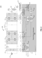
- FIG. 1 is a block diagram illustrating an example of a power delivery system according to an embodiment.
- power delivery system 100 includes power delivery subsystem 110 and power transmitting device 120 .
- Power delivery subsystem 110 may provide the interface to a power connector, such as universal serial bus (USB) connector 143 (e.g., USB Type-C port) of power transmitting device 120 .
- Subsystem 110 e.g., a USB-Power Delivery (PD) integrated circuit (IC) controller
- PD USB-Power Delivery
- IC integrated circuit
- the USB-PD specification defines a standard protocol designed to enable the maximum functionality of USB-enabled devices by providing more flexible power delivery along with data communications over a single USB cable through USB ports (e.g., USB Type-C).
- the USB-PD specification also describes the architecture, protocols, power supply behavior, parameters, and cabling necessary for managing power delivery over USB cables (e.g., up to 5 A of current at up to 20V, for a total of up to 100 W of power).
- the USB-PD specification also defines the requirements for a power delivery contract (PD contract) that can be negotiated between a pair of USB-enabled devices.
- the PD contract can specify both the power level and the direction of power transfer that can be accommodated by both devices, and can be dynamically re-negotiated (e.g., without device un-plugging).
- power transmitting device 120 may include buck-boost stage 141 , inverter stage 142 , USB connector 143 (e.g., USB Type-C connector), and transmitting coil 144 .
- buck-boost stage 141 when a power receiving device (e.g., a device to be wirelessly charged) having a receiving coil is placed in proximity of the power transmitting device 120 , AC power signal from transmitting coil 144 is inductively coupled to the receiving coil, thereby enabling transmitting coil 144 to transfer power to the receiving coil of the power receiving device.
- a power receiving device e.g., a device to be wirelessly charged
- AC power signal from transmitting coil 144 is inductively coupled to the receiving coil, thereby enabling transmitting coil 144 to transfer power to the receiving coil of the power receiving device.
- a foreign object may be placed in proximity of power transmitting device 120 (or no object is placed in proximity of power transmitting device 120 ), and therefore, power delivery system 100 needs to determine whether transmitting coil 144 is a free coil (i.e., transmitting coil 144 is available as no object is present), whether a receiving coil is present, or whether a foreign object is present.
- transmitting coil 144 is a free coil (i.e., transmitting coil 144 is available as no object is present), whether a receiving coil is present, or whether a foreign object is present.
- DC voltage from a buck-boost stage 141 may be supplied to inverter stage 142 (e.g., full-bridge or half-bridge inverter stage) of the power transmitting device 120 .
- the inverter stage 142 may convert the DC voltage to an AC square wave to feed a resonant tank formed by the transmitting coil 144 and a resonant capacitor (not shown).
- the power transmitting device 120 may control the voltage, frequency, phase angle or duty cycle of inverter stage 142 to regulate the power transfer (e.g., at a power receiving device).
- Operating parameters of inverter stage 142 such as output voltage and bridge current, may be a function of the frequency, coupling, DC input voltage, load of the power receiving device, coil parameters of the power receiving device, etc.
- USB connector 143 may be a power connector providing power to power transmitting device 120 .
- USB connector 143 may be configured according to the USB Type-C specification.
- USB connector 143 may negotiate power with a connected source (e.g., AC/DC adaptor) and use an integrated buck-boost controller (e.g., buck boost control logic 126 ) in “buck only” configuration to supply the required voltage and current.
- a connected source e.g., AC/DC adaptor
- buck-boost controller e.g., buck boost control logic 126
- power delivery subsystem 110 may include configuration channel (CC) comparator 121 , zero crossing detection (ZCD) comparator 122 , current sense amplifier (CSA) 123 , foreign object detection (FOD) logic 124 , inverter control logic 125 and buck boost control logic 126 .
- CC configuration channel
- ZCD zero crossing detection
- CSA current sense amplifier
- FOD foreign object detection
- inverter control logic 125 buck boost control logic 126 .
- CC comparator 121 may be configured to determine a starting point of cycle count of a decaying coil voltage waveform. That is, the output voltage of comparator 121 may be used to trigger a counter, for example, via firmware interrupt.
- FOD logic 124 may be configured to excite a resonant tank with a small pulse (also referred to as ping pulse).
- the ping pulse creates sufficient energy in the resonant tank, which may be formed by transmitting coil 144 and a resonant capacitor (not shown) connected to coil 144 , such that the resonant tank produces a decaying coil voltage waveform (e.g., decaying coil voltage waveform 603 of FIG. 6 ) after the excitation.
- the decaying coil voltage waveform may include, but not limited to, information to detect whether transmitting coil 144 is a free coil (i.e., transmitting coil 144 is available as no object is present), whether a receiving coil is present, or whether a foreign object is present.
- the reference voltage of CC comparator 121 may be set to 200 mV or any suitable voltage. In another embodiment, the reference voltage may be varied to enable multiple points of comparison using a variable reference for comparator 121 .
- ZCD comparator 122 may be configured to count a number of cycles (N cycles, where N is a positive integer) of the decaying coil voltage waveform.
- the output voltage of comparator 122 may be used for period counting, i.e., frequency measurement.
- the output of comparator 122 e.g., ZCD waveform or signal 604 of FIG. 6 which is also a decaying waveform
- the reference voltage of comparator 122 may be set to 30 mV, 60 mV or any suitable voltage.
- the reference voltage may be varied to enable multiple points of comparison using a variable reference for comparator 122 .
- FIG. 3 is a block diagram illustrating an example of the ZCD comparator 122 .
- comparator 300 may include variable offset options from 0 to 50 mV and may be configured with 3 mV or less in sensing accuracy for faster response time, though those voltage values are non-limiting.
- FOD logic 124 is configured to determine the presence of a foreign object.
- the presence of the foreign object before power delivery may reflect in form of lower Q-factor and change in resonance frequency.
- FOD logic 124 may be configured to excite a resonant tank (formed by coil 144 and a resonant capacitor) with few pulses (also referred to as ping pulses), via inverter control logic 125 and inverter stage 142 , to produce a decaying coil voltage waveform detected at coil voltage 145 .
- the excitation of the resonant tank may be variable, for example, the ping pulses may be transmitted at a random interval.
- FOD logic 124 may estimate or determine the Q-factor and resonance frequency.
- the coil voltage after excitation decays slower when a power receiving device is not present as compared to a scenario when the power receiving device or a foreign object is present on an interface surface having transmitting coil 144 .
- FOD logic 124 via power transmitting device 120 ) may measure the coil Q-factor of coil 144 .
- the use of the Q-factor and resonance frequency values can decide on the presence of a foreign object.
- FOD logic 124 may receive a reported reference Q-factor to determine an appropriate FOD threshold level.
- the FOD threshold level may be configurable or preset by a customer based on system design. If the measured Q is less than the threshold level, FOD logic 124 may determine that a foreign object is present. On the other hand, if the measured Q meets or exceeds the threshold level, FOD logic 124 may determine that there is no presence of a foreign object.
- inverter control logic (or inverter controller) 125 may provide the required output to a power receiving device by controlling the gain of the resonant tank via frequency or voltage from output of buck-boost control logic (or buck-boost controller) 126 .
- inverter controller 125 may be configured as a full bridge or half bridge inverter controller.
- buck-boost control logic (or buck-boost controller) 126 provides the required output voltage in constant voltage mode for Qi/proprietary wireless power transmitter.
- Controller 126 may be configured as buck, boost, or buck-boost controller.
- buck-boost controller 126 may implement peak current control in boost and buck mode.
- Current sense amplifier (CSA) 123 may be used for peak current sensing through an external resistor placed in VIN path (not shown) of controller 126 .
- CSA 123 may also generate a slope compensation ramp which is added on a current sense ramp signal for internal current loop stability.
- Low pass and high pass filtering 127 (which may be part of power delivery subsystem 110 or power transmitting device 120 ) attenuates the voltage at coil voltage 145 above and below, respectively, a cutoff frequency, thereby allowing lower frequencies (low pass) and/or higher frequencies (high pass) to pass through filtering 127 .
- Output from low pass and high pass filtering 127 are provided to comparators 121 - 122 as their input voltage.
- FIG. 2 is a block diagram illustrating another example of a power delivery system according to an embodiment.
- power delivery system 200 includes power delivery subsystem 240 and power transmitting device 250 .
- Power transmitting device 250 may include USB connector 220 (e.g., USB Type-C connector), electromagnetic interference (EMI) filter 221 , buck-boost stage 222 , inverter stage 223 , and transmitting coil 225 .
- USB connector 220 e.g., USB Type-C connector
- EMI electromagnetic interference
- buck-boost stage 222 buck-boost stage 222
- inverter stage 223 transmitting coil 225
- transmitting coil 225 When a power receiving device is placed in proximity of the power transmitting device 250 (e.g., on an interface surface), AC power signal from transmitting coil 225 is inductively coupled to the receiving coil of the power receiving device to enable transmitting coil 225 to transfer power to the receiving coil.
- a foreign object may be placed in proximity of power transmitting device 250 (or no object is placed in proximity of device 250 ). Therefore, as part of foreign object detection, power delivery system 200 needs to determine whether transmitting coil 225 is a free coil (i.e., transmitting
- Buck-boost stage 222 may provide DC voltage to inverter stage 223 (e.g., full-bridge or half-bridge inverter stage).
- the inverter stage 223 may convert the DC voltage to an AC square wave to feed a resonant tank formed by the transmitting coil 225 and resonant capacitor 224 .
- power transmitting device 250 may control the voltage, frequency, phase angle or duty cycle of inverter stage 223 to regulate the power transfer.
- Operating parameters of inverter stage 223 such as output voltage and bridge current, may be a function of the frequency, coupling, DC input voltage, load of the power receiving device, coil parameters of the power transmitting and receiving device, etc.
- USB connector 220 may be a power connector providing power to buck-boost stage 222 .
- USB connector 220 may be configured according to the USB Type-C specification.
- USB connector 143 may negotiate power with a connected source (e.g., AC/DC adaptor) and use buck-boost controller 202 in “buck only” configuration to supply the required voltage and current.
- signals from USB connector 220 may be supplied to EMI filter 221 (which is connected in parallel with buck-boost stage 222 through switching device Ml, e.g., a metal oxide semiconductor field-effect transistor (MOSFET)) to prevent AC switching signals present on the power core's input from reaching buck-boost stage 222 .
- MOSFET metal oxide semiconductor field-effect transistor
- Power delivery subsystem 240 may include, buck boost logic 201 , inverter control logic 202 , FOD logic 203 , ZCD comparator 204 , CC comparator 205 , pulse width modulation (PWM) ports 206 - 207 , and CSA 208 .
- PWM pulse width modulation
- ZCD comparator 204 may count a number of cycles (N cycles) of the decaying coil voltage waveform.
- the output voltage of ZCD comparator 204 may be used for period counting (that is, frequency measurement).
- the output of comparator 122 e.g., ZCD waveform (or signal) 604 of FIG. 6
- the reference voltage of comparator 204 may be set to 30 mV, 60 mV or any suitable voltage.
- the reference voltage may be varied to enable multiple points of comparison using a variable reference for comparator 204 .
- CC comparator 205 may be configured to determine a starting point of cycle count of a decaying coil voltage waveform.
- FOD logic 124 may be configured to excite transmitting coil 225 with pulses (also referred to as ping pulses). The ping pulses create energy in a resonant tank formed by transmitting coil 225 and resonant capacitor 224 to produce a decaying coil voltage waveform (e.g., decaying coil voltage waveform 603 of FIG. 6 ).
- the decaying coil voltage waveform may include, but not limited to, information to detect whether transmitting coil 225 is a free coil (i.e., transmitting coil 225 is available as no object is present), whether a receiving coil is present, or whether a foreign object is present.
- the reference voltage of CC comparator 205 may be set to 200 mV or any suitable voltage. In another embodiment, the reference voltage may be varied to enable multiple points of comparison using a variable reference for comparator 205 .
- FOD logic 203 may determine the presence of a foreign object.
- the presence of the foreign object before power delivery may reflect in form of lower Q-factor and/or change in resonance frequency.
- FOD logic 203 may excite a resonant tank (formed by coil 225 and resonant capacitor 224 ) with ping pulses (using inverter control logic 202 to send PWM signals from PWM port 207 to inverter stage 223 ) to produce a decaying coil voltage waveform at coil voltage 226 . Based on the decaying coil voltage waveform, FOD logic 203 may estimate or determine the Q-factor and resonance frequency.
- FOD logic 203 may measure the coil Q-factor of coil 225 .
- the use of the Q-factor and resonance frequency values can decide on the presence of a foreign object.
- FOD logic 203 may receive a reported reference Q-factor to determine an FOD threshold level.
- the FOD threshold level may be configurable or preset by a customer based on system design. If the measured Q is less than the threshold level, FOD logic 203 may determine that a foreign object is present. On the other hand, if the measured Q meets or exceeds the threshold level, FOD logic 124 may determine that there is no presence of a foreign object.
- Inverter control logic 202 may provide the required output to a power receiving device by controlling the gain of the resonant tank via frequency or voltage from output of buck-boost control logic 201 . Inverter control logic 202 may control the operational parameters of inverter stage 223 through PWM port 207 . In some embodiments, inverter controller 202 may be configured as a full bridge or half bridge inverter controller.
- Buck-boost control logic 201 may supply the required output voltage in constant voltage mode for Qi/proprietary wireless power transmitter.
- Logic 201 may control buck-boost stage 222 through PWM port 206 .
- Logic 201 may be configured as buck, boost, or buck-boost controller.
- logic 201 may implement peak current control in boost and buck mode.
- CSA 208 may be used for peak current sensing through an external resistor placed in PVIN_0 path of logic 201 .
- CSA 208 may also generate a slope compensation ramp which is added on a current sense ramp signal for internal current loop stability.
- Low pass and high pass filtering 207 (which may be part of power delivery subsystem 240 or power transmitting device 250 ) attenuates the voltage at coil voltage 206 above or below, respectively, a cutoff frequency to allow lower frequencies (low pass) or higher frequencies (high pass) to pass through filtering 207 .
- Output from low pass and high pass filtering 207 are provided to comparators 204 - 205 as their input voltage.
- FIG. 4 is a flow diagram illustrating an example of a method of foreign object detection according to an embodiment.
- method 400 may be performed by FOD logic 124 of FIG. 1 and FOD logic 203 of FIG. 2 .
- a decaying coil voltage signal of a transmitting coil of the wireless power delivery system is detected.
- a first comparator e.g., CC comparator
- a second comparator e.g., ZCD comparator
- a Q-factor of the transmitting coil is determined based on the number of cycles of the decaying coil voltage signal, a reference signal of the first comparator, and a reference signal of the second comparator.
- whether a foreign object is present is determined based on the Q-factor and a FOD threshold level.
- FIG. 5 is a flow diagram illustrating another example of a method of foreign object detection according to an embodiment.
- method 500 may be performed by FOD logic 124 of FIG. 1 and FOD logic 203 of FIG. 2 .
- a first comparator CMP1 (e.g., CC comparator) is setup for a first reference voltage (V1), e.g., 200 mV, rising edge interrupt on a transmitting coil (e.g., coil 144 of FIG. 1 ) resonance input.
- V1 may be a variable reference voltage to enable multiple points of comparison for CMP1. For example, each time block 502 is executed, V1 may be setup for a different voltage value.
- a second comparator CMP2 (e.g., ZCD comparator) is setup for a second reference voltage (V2), e.g., 30 mV, falling edge interrupt on the transmitting coil resonance input.
- V2 may be a variable reference voltage to enable multiple points of comparison for CMP2.
- each time block 503 is executed V2 may be setup for a different voltage value.
- a resonance timer is started then method 500 proceeds to block 515 (described herein below).
- analog PWM ping pulses are sent to excite the transmitting coil, with CMP1 status being set to False (e.g., 0) and ‘V above V1’ also being set to False (e.g., 0).
- V is the input voltage to CMP1 and CMP2 (e.g., decaying coil voltage waveform 603 of FIG. 6 ). Examples of V1 and V2 are illustrated in waveforms or signals 602 and 601 of FIG. 6 , respectively.
- CMP1 interrupt may be triggered when V is above V1. If the CMP1 interrupt is triggered, method 500 proceeds to block 507 . Otherwise, method 500 returns to block 506 .
- CMP1 status is set to True (e.g., 1) and ‘V above V1’ is also set to True (e.g., 1).
- CMP2 interrupt may be triggered when V crosses V2.
- An example of output voltage from CMP2 that triggers the CMP2 interrupt is shown in ZCD waveform 604 of FIG. 6 , which may be the negative portion of decaying coil voltage waveform 603 . If the CMP2 interrupt is triggered, method 500 proceeds to block 509 . Otherwise, method 500 returns to block 508 .
- method 500 proceeds to block 510 . Otherwise, method 500 returns to block 508 .
- method 500 it is determined whether ‘V above V1’ is True. If so method 500 proceeds to block 511 where ‘V above V1’ is set to False, then returns to block 508 . Otherwise, method 500 proceeds to block 512 where it is determined V has reached V1 and CMP1 can be stopped.
- a resonance cycles counter (N) is incremented.
- CMP2 interrupt e.g., based on output waveform of CMP2. If so, method 500 returns to block 513 to increment the resonance cycles counter again. Otherwise, method 500 proceeds block 515 .
- method 500 proceeds to block 516 . Otherwise, method 500 returns to block 514 .
- method 500 ends the resonance and stops CMP2.
- method 500 proceeds to block 519 . Otherwise, method 500 proceeds to block 518 .
- a Q-factor is calculated according to the following:
- method 500 returns to block 502 .
- Various units, circuits, or other components may be described or claimed as “configured to” or “configurable to” perform a task or tasks.
- the phrase “configured to” or “configurable to” is used to connote structure by indicating that the units/circuits/components include structure (e.g., circuitry) that performs the task or tasks during operation.
- the unit/circuit/component can be said to be configured to perform the task, or configurable to perform the task, even when the specified unit/circuit/component is not currently operational (e.g., is not on).
- the units/circuits/components used with the “configured to” or “configurable to” language include hardware—for example, circuits, memory storing program instructions executable to implement the operation, etc. Reciting that a unit/circuit/component is “configured to” perform one or more tasks, or is “configurable to” perform one or more tasks, is expressly intended not to invoke 35 U.S.C. 112(f) or 35 U.S.C. 112, sixth paragraph, for that unit/circuit/component.
- processing logic that comprises hardware (e.g. circuitry, dedicated logic, etc.), software (e.g., embodied on a non-transitory computer readable medium), or a combination of both.
- processing logic comprises hardware (e.g. circuitry, dedicated logic, etc.), software (e.g., embodied on a non-transitory computer readable medium), or a combination of both.
- Embodiments of the present disclosure are not described with reference to any particular programming language. It will be appreciated that a variety of programming languages may be used to implement the teachings of embodiments of the invention as described herein.
Landscapes
- Engineering & Computer Science (AREA)
- Power Engineering (AREA)
- Computer Networks & Wireless Communication (AREA)
- Physics & Mathematics (AREA)
- Life Sciences & Earth Sciences (AREA)
- Remote Sensing (AREA)
- Electromagnetism (AREA)
- Environmental & Geological Engineering (AREA)
- Geology (AREA)
- General Life Sciences & Earth Sciences (AREA)
- General Physics & Mathematics (AREA)
- Geophysics (AREA)
- Near-Field Transmission Systems (AREA)
Abstract
Description
Claims (20)
Priority Applications (3)
| Application Number | Priority Date | Filing Date | Title |
|---|---|---|---|
| US17/669,113 US11936207B2 (en) | 2022-02-10 | 2022-02-10 | Foreign object detection using decay counter for Q-estimation |
| DE102023102790.5A DE102023102790A1 (en) | 2022-02-10 | 2023-02-06 | DETECTION OF FOREIGN OBJECTS USING A DECAY COUNTER FOR Q ESTIMATION |
| CN202310079653.2A CN116581902A (en) | 2022-02-10 | 2023-02-08 | Foreign Object Detection Using Decay Counters for Q Estimation |
Applications Claiming Priority (1)
| Application Number | Priority Date | Filing Date | Title |
|---|---|---|---|
| US17/669,113 US11936207B2 (en) | 2022-02-10 | 2022-02-10 | Foreign object detection using decay counter for Q-estimation |
Publications (2)
| Publication Number | Publication Date |
|---|---|
| US20230253836A1 US20230253836A1 (en) | 2023-08-10 |
| US11936207B2 true US11936207B2 (en) | 2024-03-19 |
Family
ID=87312629
Family Applications (1)
| Application Number | Title | Priority Date | Filing Date |
|---|---|---|---|
| US17/669,113 Active 2042-10-01 US11936207B2 (en) | 2022-02-10 | 2022-02-10 | Foreign object detection using decay counter for Q-estimation |
Country Status (3)
| Country | Link |
|---|---|
| US (1) | US11936207B2 (en) |
| CN (1) | CN116581902A (en) |
| DE (1) | DE102023102790A1 (en) |
Citations (16)
| Publication number | Priority date | Publication date | Assignee | Title |
|---|---|---|---|---|
| US20150097442A1 (en) * | 2013-10-08 | 2015-04-09 | Nokia Corporation | Method and apparatus for wireless power transfer |
| US20150108849A1 (en) * | 2012-05-02 | 2015-04-23 | Powerbyproxi Limited | Method for detecting and identifying a receiver in an inductive power transfer system |
| US20150123606A1 (en) * | 2013-11-04 | 2015-05-07 | Amphenol Tecvox, LLC | Wireless Charging System with Data Tunneling |
| US20160141882A1 (en) * | 2013-06-19 | 2016-05-19 | Renesas Electronics Corporation | Power transmission device, wireless power feeding system, and control method |
| US20160149442A1 (en) * | 2014-03-05 | 2016-05-26 | Panasonic Intellectual Property Management Co., Ltd. | Foreign object detector, power transmitter, power receiver, and wireless power transmission system |
| US20180097401A1 (en) * | 2016-09-30 | 2018-04-05 | Steven G. Gaskill | Multiple coils for wireless power |
| US20180131235A1 (en) * | 2016-11-10 | 2018-05-10 | Rohm Co., Ltd. | Wireless power transmission apparatus and control method for the same |
| US20190337404A1 (en) * | 2017-02-09 | 2019-11-07 | Panasonic Intellectual Property Management Co., Ltd. | Method for controlling power transmitting device in wireless power transmission system and power transmitting device |
| US10978921B1 (en) * | 2020-03-25 | 2021-04-13 | Apple Inc. | Wireless power system with efficiency prediction |
| US20210351631A1 (en) * | 2020-05-11 | 2021-11-11 | Samsung Electronics Co., Ltd. | Electronic device for wirelessly transmitting or receiving power and method for operating the same |
| US20220352761A1 (en) * | 2021-04-30 | 2022-11-03 | Nucurrent, Inc. | Power Capability Detection With Verification Load In Power Level Control Systems For Wireless Power Transmission |
| US20230052693A1 (en) * | 2021-08-13 | 2023-02-16 | Samsung Electronics Co., Ltd. | Method of detecting foreign object and electronic device |
| US20230082647A1 (en) * | 2020-05-22 | 2023-03-16 | Canon Kabushiki Kaisha | Power transmitting apparatus, power receiving apparatus, control method, and storage medium |
| US20230097511A1 (en) * | 2020-05-08 | 2023-03-30 | Canon Kabushiki Kaisha | Power receiving apparatus, power transmitting apparatus, control method, and storage medium |
| US20230238836A1 (en) * | 2022-01-24 | 2023-07-27 | Hitachi-Lg Data Storage Korea, Inc. | Apparatus and method for transmitting power wirelessly |
| US20230369892A1 (en) * | 2019-02-05 | 2023-11-16 | Mojo Mobility Inc. | System and method for infrastructure, vehicle and internet of things wireless chargers |
-
2022
- 2022-02-10 US US17/669,113 patent/US11936207B2/en active Active
-
2023
- 2023-02-06 DE DE102023102790.5A patent/DE102023102790A1/en active Pending
- 2023-02-08 CN CN202310079653.2A patent/CN116581902A/en active Pending
Patent Citations (16)
| Publication number | Priority date | Publication date | Assignee | Title |
|---|---|---|---|---|
| US20150108849A1 (en) * | 2012-05-02 | 2015-04-23 | Powerbyproxi Limited | Method for detecting and identifying a receiver in an inductive power transfer system |
| US20160141882A1 (en) * | 2013-06-19 | 2016-05-19 | Renesas Electronics Corporation | Power transmission device, wireless power feeding system, and control method |
| US20150097442A1 (en) * | 2013-10-08 | 2015-04-09 | Nokia Corporation | Method and apparatus for wireless power transfer |
| US20150123606A1 (en) * | 2013-11-04 | 2015-05-07 | Amphenol Tecvox, LLC | Wireless Charging System with Data Tunneling |
| US20160149442A1 (en) * | 2014-03-05 | 2016-05-26 | Panasonic Intellectual Property Management Co., Ltd. | Foreign object detector, power transmitter, power receiver, and wireless power transmission system |
| US20180097401A1 (en) * | 2016-09-30 | 2018-04-05 | Steven G. Gaskill | Multiple coils for wireless power |
| US20180131235A1 (en) * | 2016-11-10 | 2018-05-10 | Rohm Co., Ltd. | Wireless power transmission apparatus and control method for the same |
| US20190337404A1 (en) * | 2017-02-09 | 2019-11-07 | Panasonic Intellectual Property Management Co., Ltd. | Method for controlling power transmitting device in wireless power transmission system and power transmitting device |
| US20230369892A1 (en) * | 2019-02-05 | 2023-11-16 | Mojo Mobility Inc. | System and method for infrastructure, vehicle and internet of things wireless chargers |
| US10978921B1 (en) * | 2020-03-25 | 2021-04-13 | Apple Inc. | Wireless power system with efficiency prediction |
| US20230097511A1 (en) * | 2020-05-08 | 2023-03-30 | Canon Kabushiki Kaisha | Power receiving apparatus, power transmitting apparatus, control method, and storage medium |
| US20210351631A1 (en) * | 2020-05-11 | 2021-11-11 | Samsung Electronics Co., Ltd. | Electronic device for wirelessly transmitting or receiving power and method for operating the same |
| US20230082647A1 (en) * | 2020-05-22 | 2023-03-16 | Canon Kabushiki Kaisha | Power transmitting apparatus, power receiving apparatus, control method, and storage medium |
| US20220352761A1 (en) * | 2021-04-30 | 2022-11-03 | Nucurrent, Inc. | Power Capability Detection With Verification Load In Power Level Control Systems For Wireless Power Transmission |
| US20230052693A1 (en) * | 2021-08-13 | 2023-02-16 | Samsung Electronics Co., Ltd. | Method of detecting foreign object and electronic device |
| US20230238836A1 (en) * | 2022-01-24 | 2023-07-27 | Hitachi-Lg Data Storage Korea, Inc. | Apparatus and method for transmitting power wirelessly |
Also Published As
| Publication number | Publication date |
|---|---|
| DE102023102790A1 (en) | 2023-08-10 |
| US20230253836A1 (en) | 2023-08-10 |
| DE102023102790A8 (en) | 2023-10-05 |
| CN116581902A (en) | 2023-08-11 |
Similar Documents
| Publication | Publication Date | Title |
|---|---|---|
| US11283308B2 (en) | Methods for detecting and identifying a receiver in an inductive power transfer system | |
| CN110391697B (en) | Method and device for performing foreign body detection | |
| US7511460B1 (en) | Circuits, systems, methods, and software for power factor correction and/or control | |
| US9455644B2 (en) | Method and apparatus for changing a frequency of a switch prior to a level of current received from an inductor decreasing to a predetermined level | |
| US20180131235A1 (en) | Wireless power transmission apparatus and control method for the same | |
| US9680382B2 (en) | Input frequency measurement | |
| EP2950423A1 (en) | Power transmitting device and wireless power transmission system | |
| US10218211B2 (en) | Determination of Q-factor of resonant tank network | |
| US20260058499A1 (en) | Foreign object detection and related apparatuses, methods, and systems | |
| US11936207B2 (en) | Foreign object detection using decay counter for Q-estimation | |
| US12519347B2 (en) | Foreign object detection by frequency bandwidth comparison | |
| CN114825948B (en) | Control circuit and control method of power adapter and power adapter | |
| US20250183714A1 (en) | Displaced receiver detection in a wireless power system and related apparatuses, methods, and systems | |
| TW200415842A (en) | Direct voltage-direct voltage converter | |
| JP2019083685A (en) | Method of detecting receiver and inductive power transmission system | |
| CN108808892A (en) | Metal foreign matter detection method of induction type power supply and power supply module thereof | |
| WO2025053872A1 (en) | Foreign object detection by frequency bandwidth comparison |
Legal Events
| Date | Code | Title | Description |
|---|---|---|---|
| FEPP | Fee payment procedure |
Free format text: ENTITY STATUS SET TO UNDISCOUNTED (ORIGINAL EVENT CODE: BIG.); ENTITY STATUS OF PATENT OWNER: LARGE ENTITY |
|
| STPP | Information on status: patent application and granting procedure in general |
Free format text: DOCKETED NEW CASE - READY FOR EXAMINATION |
|
| AS | Assignment |
Owner name: CYPRESS SEMICONDUCTOR CORPORATION, CALIFORNIA Free format text: ASSIGNMENT OF ASSIGNORS INTEREST;ASSIGNORS:TUDU, RUSHIKA BANAM BALIA;KEDILAYA, VISHWAS;NAGAMANGALA MUNINARAYANAPPA, JEEVITH KUMAR;AND OTHERS;SIGNING DATES FROM 20220201 TO 20230425;REEL/FRAME:064592/0088 |
|
| STPP | Information on status: patent application and granting procedure in general |
Free format text: NOTICE OF ALLOWANCE MAILED -- APPLICATION RECEIVED IN OFFICE OF PUBLICATIONS |
|
| STPP | Information on status: patent application and granting procedure in general |
Free format text: PUBLICATIONS -- ISSUE FEE PAYMENT VERIFIED |
|
| STCF | Information on status: patent grant |
Free format text: PATENTED CASE |
|
| AS | Assignment |
Owner name: INFINEON TECHNOLOGIES AMERICAS CORP., CALIFORNIA Free format text: MERGER;ASSIGNOR:CYPRESS SEMICONDUCTOR CORPORATION;REEL/FRAME:073571/0456 Effective date: 20250926 |