US11469222B2 - ESD-protection device and MOS-transistor having at least one integrated ESD-protection device - Google Patents
ESD-protection device and MOS-transistor having at least one integrated ESD-protection device Download PDFInfo
- Publication number
- US11469222B2 US11469222B2 US16/834,680 US202016834680A US11469222B2 US 11469222 B2 US11469222 B2 US 11469222B2 US 202016834680 A US202016834680 A US 202016834680A US 11469222 B2 US11469222 B2 US 11469222B2
- Authority
- US
- United States
- Prior art keywords
- region
- doped region
- reaion
- doped
- well
- Prior art date
- Legal status (The legal status is an assumption and is not a legal conclusion. Google has not performed a legal analysis and makes no representation as to the accuracy of the status listed.)
- Active
Links
Images


Classifications
-
- H—ELECTRICITY
- H10—SEMICONDUCTOR DEVICES; ELECTRIC SOLID-STATE DEVICES NOT OTHERWISE PROVIDED FOR
- H10D—INORGANIC ELECTRIC SEMICONDUCTOR DEVICES
- H10D62/00—Semiconductor bodies, or regions thereof, of devices having potential barriers
- H10D62/10—Shapes, relative sizes or dispositions of the regions of the semiconductor bodies; Shapes of the semiconductor bodies
- H10D62/102—Constructional design considerations for preventing surface leakage or controlling electric field concentration
- H10D62/103—Constructional design considerations for preventing surface leakage or controlling electric field concentration for increasing or controlling the breakdown voltage of reverse-biased devices
- H10D62/105—Constructional design considerations for preventing surface leakage or controlling electric field concentration for increasing or controlling the breakdown voltage of reverse-biased devices by having particular doping profiles, shapes or arrangements of PN junctions; by having supplementary regions, e.g. junction termination extension [JTE]
- H10D62/109—Reduced surface field [RESURF] PN junction structures
-
- H01L27/0262—
-
- H—ELECTRICITY
- H10—SEMICONDUCTOR DEVICES; ELECTRIC SOLID-STATE DEVICES NOT OTHERWISE PROVIDED FOR
- H10D—INORGANIC ELECTRIC SEMICONDUCTOR DEVICES
- H10D18/00—Thyristors
- H10D18/01—Manufacture or treatment
-
- H—ELECTRICITY
- H10—SEMICONDUCTOR DEVICES; ELECTRIC SOLID-STATE DEVICES NOT OTHERWISE PROVIDED FOR
- H10D—INORGANIC ELECTRIC SEMICONDUCTOR DEVICES
- H10D62/00—Semiconductor bodies, or regions thereof, of devices having potential barriers
- H10D62/10—Shapes, relative sizes or dispositions of the regions of the semiconductor bodies; Shapes of the semiconductor bodies
- H10D62/13—Semiconductor regions connected to electrodes carrying current to be rectified, amplified or switched, e.g. source or drain regions
- H10D62/141—Anode or cathode regions of thyristors; Collector or emitter regions of gated bipolar-mode devices, e.g. of IGBTs
- H10D62/148—Cathode regions of thyristors
-
- H—ELECTRICITY
- H10—SEMICONDUCTOR DEVICES; ELECTRIC SOLID-STATE DEVICES NOT OTHERWISE PROVIDED FOR
- H10D—INORGANIC ELECTRIC SEMICONDUCTOR DEVICES
- H10D62/00—Semiconductor bodies, or regions thereof, of devices having potential barriers
- H10D62/10—Shapes, relative sizes or dispositions of the regions of the semiconductor bodies; Shapes of the semiconductor bodies
- H10D62/17—Semiconductor regions connected to electrodes not carrying current to be rectified, amplified or switched, e.g. channel regions
- H10D62/393—Body regions of DMOS transistors or IGBTs
-
- H—ELECTRICITY
- H10—SEMICONDUCTOR DEVICES; ELECTRIC SOLID-STATE DEVICES NOT OTHERWISE PROVIDED FOR
- H10D—INORGANIC ELECTRIC SEMICONDUCTOR DEVICES
- H10D64/00—Electrodes of devices having potential barriers
- H10D64/20—Electrodes characterised by their shapes, relative sizes or dispositions
- H10D64/27—Electrodes not carrying the current to be rectified, amplified, oscillated or switched, e.g. gates
- H10D64/311—Gate electrodes for field-effect devices
- H10D64/411—Gate electrodes for field-effect devices for FETs
- H10D64/511—Gate electrodes for field-effect devices for FETs for IGFETs
- H10D64/514—Gate electrodes for field-effect devices for FETs for IGFETs characterised by the insulating layers
- H10D64/516—Gate electrodes for field-effect devices for FETs for IGFETs characterised by the insulating layers the thicknesses being non-uniform
-
- H—ELECTRICITY
- H10—SEMICONDUCTOR DEVICES; ELECTRIC SOLID-STATE DEVICES NOT OTHERWISE PROVIDED FOR
- H10D—INORGANIC ELECTRIC SEMICONDUCTOR DEVICES
- H10D84/00—Integrated devices formed in or on semiconductor substrates that comprise only semiconducting layers, e.g. on Si wafers or on GaAs-on-Si wafers
- H10D84/101—Integrated devices comprising main components and built-in components, e.g. IGBT having built-in freewheel diode
- H10D84/131—Thyristors having built-in components
-
- H—ELECTRICITY
- H10—SEMICONDUCTOR DEVICES; ELECTRIC SOLID-STATE DEVICES NOT OTHERWISE PROVIDED FOR
- H10D—INORGANIC ELECTRIC SEMICONDUCTOR DEVICES
- H10D84/00—Integrated devices formed in or on semiconductor substrates that comprise only semiconducting layers, e.g. on Si wafers or on GaAs-on-Si wafers
- H10D84/101—Integrated devices comprising main components and built-in components, e.g. IGBT having built-in freewheel diode
- H10D84/151—LDMOS having built-in components
-
- H—ELECTRICITY
- H10—SEMICONDUCTOR DEVICES; ELECTRIC SOLID-STATE DEVICES NOT OTHERWISE PROVIDED FOR
- H10D—INORGANIC ELECTRIC SEMICONDUCTOR DEVICES
- H10D89/00—Aspects of integrated devices not covered by groups H10D84/00 - H10D88/00
- H10D89/60—Integrated devices comprising arrangements for electrical or thermal protection, e.g. protection circuits against electrostatic discharge [ESD]
- H10D89/601—Integrated devices comprising arrangements for electrical or thermal protection, e.g. protection circuits against electrostatic discharge [ESD] for devices having insulated gate electrodes, e.g. for IGFETs or IGBTs
- H10D89/711—Integrated devices comprising arrangements for electrical or thermal protection, e.g. protection circuits against electrostatic discharge [ESD] for devices having insulated gate electrodes, e.g. for IGFETs or IGBTs using bipolar transistors as protective elements
- H10D89/713—Integrated devices comprising arrangements for electrical or thermal protection, e.g. protection circuits against electrostatic discharge [ESD] for devices having insulated gate electrodes, e.g. for IGFETs or IGBTs using bipolar transistors as protective elements including a PNP transistor and a NPN transistor, wherein each of said transistors has its base region coupled to the collector region of the other transistor, e.g. silicon controlled rectifier [SCR] devices
-
- H—ELECTRICITY
- H10—SEMICONDUCTOR DEVICES; ELECTRIC SOLID-STATE DEVICES NOT OTHERWISE PROVIDED FOR
- H10D—INORGANIC ELECTRIC SEMICONDUCTOR DEVICES
- H10D89/00—Aspects of integrated devices not covered by groups H10D84/00 - H10D88/00
- H10D89/60—Integrated devices comprising arrangements for electrical or thermal protection, e.g. protection circuits against electrostatic discharge [ESD]
- H10D89/601—Integrated devices comprising arrangements for electrical or thermal protection, e.g. protection circuits against electrostatic discharge [ESD] for devices having insulated gate electrodes, e.g. for IGFETs or IGBTs
- H10D89/811—Integrated devices comprising arrangements for electrical or thermal protection, e.g. protection circuits against electrostatic discharge [ESD] for devices having insulated gate electrodes, e.g. for IGFETs or IGBTs using FETs as protective elements
- H10D89/813—Integrated devices comprising arrangements for electrical or thermal protection, e.g. protection circuits against electrostatic discharge [ESD] for devices having insulated gate electrodes, e.g. for IGFETs or IGBTs using FETs as protective elements specially adapted to provide an electrical current path other than the field-effect induced current path
-
- H—ELECTRICITY
- H10—SEMICONDUCTOR DEVICES; ELECTRIC SOLID-STATE DEVICES NOT OTHERWISE PROVIDED FOR
- H10D—INORGANIC ELECTRIC SEMICONDUCTOR DEVICES
- H10D18/00—Thyristors
- H10D18/40—Thyristors with turn-on by field effect
-
- H—ELECTRICITY
- H10—SEMICONDUCTOR DEVICES; ELECTRIC SOLID-STATE DEVICES NOT OTHERWISE PROVIDED FOR
- H10D—INORGANIC ELECTRIC SEMICONDUCTOR DEVICES
- H10D62/00—Semiconductor bodies, or regions thereof, of devices having potential barriers
- H10D62/10—Shapes, relative sizes or dispositions of the regions of the semiconductor bodies; Shapes of the semiconductor bodies
- H10D62/113—Isolations within a component, i.e. internal isolations
- H10D62/115—Dielectric isolations, e.g. air gaps
Definitions
- the present disclosure (and the claims) relate to a high-voltage device, in particular a semiconductor protection device for protection against electrostatic discharges or an MOS transistor, preferably a lateral N-channel DMOS transistor (NLDMOS) or an NMOS transistor, with an integrated semiconductor protection device.
- a semiconductor protection device for protection against electrostatic discharges or an MOS transistor preferably a lateral N-channel DMOS transistor (NLDMOS) or an NMOS transistor, with an integrated semiconductor protection device.
- ESD electrostatic discharge
- the base-emitter junction of the parasitic bipolar transistor is here switched on by the voltage drop across the bulk resistor R PW as a result of a hole current generated at the pn junction between the bulk region and the drain extension region either by impact ionization or by a dV/dt displacement current. Uneven triggering and inhomogeneous current distribution during bipolar operation will then typically quickly lead to damage by a local thermal breakdown. It follows that, at least for higher demands on the ESD resistance, a parallel-connected ESD protection device is usually required, which switches on in time and discharges the ESD pulse before damage will be caused to the HV transistor.
- Common ESD protection devices are, for example, thyristor devices of the type shown in FIGS. 4 and 5 .
- a thyristor (or SCR—Silicon Controlled Rectifier, also known as a four-layer diode) can be regarded as a combination of an NPN and a PNP transistor.
- the NPN or the PNP is switched on by a pn breakdown, a dV/dt-displacement current or an external trigger circuit. The collector current of this transistor switched on first will then switch on the respective other transistor and a state will be reached in which the NPN and PNP transistors mutually keep each other in a switched-on state.
- a high ESD strength per width can be achieved, usually expressed as failure voltage per width (in V/ ⁇ m) or per area (in V/ ⁇ m 2 ) according to the Human Body Model (HBM) or as failure current per width (in mA/ ⁇ m) or per area (in mA/ ⁇ m 2 ) measured with 100 ns current pulses by means of TLP (Transmission Line Pulsing).
- HBM Human Body Model
- Typical values are in the range from 30 to 60 mA/um for thyristor devices with voltage ranges of up to about 100V.
- Measures to reduce this risk comprise e.g. increasing the holding voltage by means of suitable changes in process and layout or stacking of a plurality of thyristors or increasing the trigger current by using a two-stage ESD protection circuit or a dynamic trigger circuit, which will switch on the thyristor only in the event of ESD.
- the effectiveness of these measures is limited, in particular in bulk CMOS processes.
- a device which is derived from an NLDMOS and in which a Pdiff region (also P+ region) is arranged close to the drain connection region acting as PNP emitter or anode of a thyristor, shown in FIGS. 6 and 7 .
- Pdiff region also P+ region
- FIGS. 6 and 7 Such a device is usually referred to as an SCR-LDMOS.
- ESD protection device it can protect a parallel-connected NLDMOS.
- the device for protection against electrostatic discharges is provided with an integrated semiconductor protection device, comprising
- an inner region configured at least as a thyristor (SCR);
- At least one outer region configured at least as a PNP transistor and adapted to protect against electrostatic discharges (ESD), the inner region and the at least one outer region being arranged adjacent to one another.
- ESD electrostatic discharges
- the outer region is preferably configured as a corner region.
- a production method for such a device achieves the same object.
- An example is a method of producing a device or an MOS transistor with protection against electrostatic discharges and with an integrated semiconductor protection device, the device comprising
- an inner region configured at least as a thyristor (SCR);
- At least one outer region configured at least as a PNP transistor and adapted to protect against electrostatic discharges (ESD), the inner region ( 1 ) and the at least one outer region ( 2 a, 2 b ) being arranged adjacent to one another,
- the production method according to the example comprises arranging on a p-type substrate at least one first N-well and arranging further sections by producing respective center-symmetrical paths and layers.
- the outer region may be a corner region.
- the device according to the present invention comprises an inner region configured at least as a thyristor (SCR), and at least one outer region, in particular a corner region, configured at least as a PNP transistor and adapted to protect against electrostatic discharges (ESD), the inner region and the at least one outer region being arranged in juxtaposition or adjacent to one another.
- SCR thyristor
- ESD electrostatic discharges
- the method according to the present invention used for producing a semiconductor protection device or an MOS transistor according to the present invention comprises arranging on a p-type substrate at least one first N-well and arranging further sections by producing respective center-symmetrical paths and layers.
- a floating connection (n.c.) in the sense of the present invention in particular a floating drain or a floating anode, is not conductively connected to any external potential.
- a main axis in the sense of the present invention may be a mirror axis of a three-dimensional body, in particular of a section according to the present invention.
- a section in the sense of the present invention is a part of the inner or outer region, which extends three-dimensionally and especially comprises a semiconductor material.
- a width of the outer region may be larger in the longitudinal direction of the device than the equally directed direction of extension of the inner region.
- An advantage of the device described here is that, due to the effect of the PNP transistor integrated in the device as a first ESD protection stage in the outer region, the SCR trigger current can greatly be increased, without the trigger voltage of the device increasing excessively. This allows use as an ESD protection device—also with dynamic triggering—while considerably reducing the risk of triggering by interference pulses and the risk of latch-up.
- the PNP transistor located in at least one corner region and the thyristor located in the inner region.
- the PNP transistor prevents the formation of a parasitic NPN transistor or of a thyristor in the at least one corner region, which would otherwise lead to high current densities and resultant thermal damage due to premature triggering in this region.
- the PNP transistor triggers before the thyristor (SCR) in the inner region and thus acts as a first ESD protection stage having an inreased holding voltage in the function process due to the low snapback that is typical of PNP transistors.
- the holding voltage is higher than half the trigger voltage of the function.
- the collector current of the PNP transistor in the outer region does not contribute to the triggering of the NPN transistor in the inner region. Even after the NPN transistor has been switched on in the inner region, the charge carrier concentration required for conductivity modulation and, consequently, the ignition of the thyristor (SCR) provided in the inner region will not be reached in the inner region, if the PNP collector current component is large in the corner region(s). This means that the low holding voltage typical of thyristors are reached only at higher currents, in particular at 200 mA, 300 mA or more than 400 mA.
- sections of the at least one inner region and sections of the at least one outer region, each consisting of semiconductor materials are oriented parallel to one another substantially in the direction of their longer main axis.
- the inner region may comprise the sections following hereinafter.
- At least one first n-doped region adapted to have connected thereto at least one drain; at least one first p-doped region arranged next to the at least one first n-doped region and adapted to have connected thereto at least one anode, the at least one first p-doped region being arranged at the at least first n-doped region according to a preferred embodiment.
- the inner region may comprise at least one first N-well having arranged therein the first n-doped region and the at least one first p-doped region.
- the inner region may comprise the following section: a second n-doped region arranged in spaced relationship with the at least one first n-doped region and/or the at least one first p-doped region and adapted to have connected thereto a source.
- the inner region may comprise the following section: at least one second p-doped region arranged next to the at least one second n-doped region and adapted to have connected thereto a bulk, the at least one second p-doped region being in particular arranged at the at least one second n-doped region.
- the inner region may comprise the following section: at least one P-well having arranged therein the at least one second n-doped region and the at least one second p-doped region, the at least one P-well being in particular arranged in the at least one first N-well and/or adjacent to the latter.
- At least one isolation region arranged between the at least one first n-doped region and/or the at least one first p-doped region and the at least one second n-doped region may be provided, a gate being connectable above this isolation region.
- the isolation region may be located above the N-well (as a drain extension region).
- the gate may be located partially above the isolation region and partially directly above the N-well and the P-well (as a bulk region).
- the thyristor may be formed in the inner region by the at least one first p-doped region, the at least one first N-well, the at least one P-well and the at least one second n-doped region.
- the at least one outer region may comprise the following sections: at least one first p-doped region (adapted to have connected thereto at least one anode); at least one first N-well (having arranged therein in particular the first n-doped region and the at least one first p-doped region).
- the at least one outer region may comprise the following section: at least one second p-doped region (adapted to have connected thereto a bulk); at least one P-well (having arranged therein the at least one second p-doped region).
- the at least one P-well is arranged in the at least one first N-well and/or adjacent to the latter.
- the at least one outer region may comprise the following section: the PNP transistor is formed in the outer region by the at least one first p-doped region, the at least one first N-well and the at least one P-well.
- at least one isolation region is provided, which is arranged between the at least one first n-doped region and/or the at least one first p-doped region and the at least one second p-doped region.
- the production of the device is substantially simplified and individual sections can be configured as common sections in both regions.
- the at least one outer region further comprises: a second n-doped region arranged in spaced relationship with the at least one first n-doped region and/or the at least one first p-doped region (the second n-doped region being connectable to a source); at least one first n-doped region (connectable to a drain), and/or at least one isolation region arranged between the at least one first n-doped region and/or the at least one first p-doped region and the second n-doped region.
- a gate may be arranged above the isolation region, the first p-doped region being arranged next to the at least one first n-doped region, in particular directly next to this n-type region.
- At least one section of the at least one outer region is configured as a common section with a corresponding section of the inner region.
- the device according to the present invention comprises at least one p-doped region arranged between the at least one first n-doped region and the at least one P-well, the p-doped region being in particular arranged in the at least one outer region directly at the at least one P-well and configured to act as a collector of the PNP-transistor.
- the device according to the present invention comprises a p-doped, in particular a highly doped, region arranged in the at least one P-well, this region being in particular arranged below the at least one second p-doped region.
- the p-doped region may preferably be a region doped with a concentration of 10 13 /cm 2 to 10 14 /cm 2 and it may in particular be arranged below the at least one second p-doped region.
- the at least one first n-doped region and/or the at least one first p-doped region is/are arranged in at least one second N-well, which is in particular arranged in the at least one first N-well and which has in particular a higher doping concentration than the at least one first N-well.
- the at least one first n-doped region (D-N+, D-N+) and/or the at least one first p-doped region (A-P+, A-P+) may be arranged in the second N-well (NWELL, NWELL), which is arranged in a first N-well (HV-NWELL, HV-NWELL).
- the second N-well may have a higher doping concentration than the at least one first N-well (HV-NWELL).
- the device according to the present invention comprises two respective source regions and two respective second n-doped regions.
- the device comprises only a respective single one of all the other sections and/or all the sections of the device are arranged or configured in a center-symmetrical, in particular convex manner.
- the device may comprise only a respective single one of them.
- All the sections may be arranged or configured in a center-symmetrical manner.
- the inner region is arranged between two outer regions. This is particularly advantageous as regards space utilization, since a semiconductor protection device of high efficiency with large PNP transistor regions is created. It will be able to dissipate high currents without damage being caused.
- the at least one first n-doped region is configured as a region with a floating potential (n.c.).
- the MOS transistor is configured as a depletion field effect transistor.
- a resistor is connected between the gate and the source, the resistor having preferably a resistance that is equal to or higher than 10 k ⁇ , and particularly preferred it has a variable resistance (in the sense of variability). This serves the purpose of dynamic triggering with capacitive gate coupling.
- the bulk and the source and/or the drain and the anode are short-circuited.
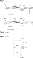
- FIG. 1 is an integrated HV-NLDMOS transistor according to the prior art
- FIG. 2 shows an integrated HV-NMOS transistor according to the prior art
- FIG. 3 is an equivalent circuit diagram of the HV-NLDMOS transistor of FIG. 1 ;
- FIG. 4 is an integrated HV-ESD protection device configured as a silicon controlled rectifier or thyristor (aka SCR) for integrated high-voltage MOS transistors in CMOS circuits according to the prior art;
- SCR silicon controlled rectifier or thyristor
- FIG. 5 is an equivalent circuit diagram of the protection device of FIG. 4 .
- FIG. 6 is an LDMOS transistor with integrated thyristor according to the prior art
- FIG. 7 is an equivalent circuit diagram of the device of FIG. 6 .
- FIG. 8 is a device according to a first embodiment of the present invention.
- FIG. 9 is a section through an outer region of the device of the first embodiment according to FIG. 8 ;
- FIG. 10 is an equivalent circuit diagram of a device according to FIG. 8 ;
- FIG. 11 is a schematic representation of the quasi-static high current characteristic curves of the device of the first embodiment of the present invention according to FIG. 8 in comparison with the device according to FIG. 6 ;
- FIG. 12 is an equivalent circuit diagram of the device of the first embodiment according to FIG. 8 with an external resistor R for dynamic triggering;
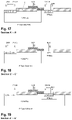
- FIG. 13 is a section through an inner region of the device of a second embodiment of the present invention with an additional P-resurf region;
- FIG. 14 is a section through an outer region of the device of the second embodiment of the present invention with an additional P-resurf region;
- FIG. 15 shows a section through an inner region of the device of a third embodiment of the present invention with an additional doping of a P-well in the bulk region;
- FIG. 16 shows a section through an outer region of the device of the third embodiment of the present invention with an additional doping of a P-well in the bulk area;
- FIG. 17 shows a section through the inner region of the device of a fourth embodiment of the present invention, with a P-well of the bulk region being located in the p-type substrate;
- FIG. 18 shows a section through the outer region of the device of the fourth embodiment of the present invention, with a P-well of the bulk region being located in the p-type substrate.
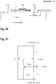
- FIG. 19 shows a section through the inner region of the device of a fifth embodiment of the present invention, which is particularly suitable for use as an ESD protection device;
- FIG. 20 shows a section through the outer region of the device of the fifth embodiment of the present invention.
- FIG. 21 is an equivalent circuit diagram of the device of the fifth embodiment of the present invention according to FIG. 19 and FIG. 20 ;
- FIG. 22 is an equivalent circuit diagram of the device of the fifth embodiment of the present invention according to FIG. 19 and FIG. 20 with an external resistor;
- FIG. 23 shows a section through the inner region of the device of a sixth embodiment of the present invention with an additional doping of a P-well in the bulk region;
- FIG. 24 shows a section through the outer region of the device of the sixth embodiment of the present invention with an additional doping of a P-well in the bulk region;
- FIG. 25 shows a section through the inner region of the device of a seventh embodiment of the present invention with a second N-well in the drain extension region;
- FIG. 26 shows a section through the outer region of the device of the seventh embodiment of the present invention.
- a first embodiment of the device according to the present invention which can be used both as a transistor with an integrated ESD protection device and as an ESD protection device alone, will be explained in more detail with reference to FIG. 8 and FIG. 9 .
- the device consists of an inner region 1 and two outer regions 2 a, 2 b, which are realized by corner regions.
- the drain region D-N+ of the transistor is preferably arranged inside, when seen in the radial direction of the device, while the source region S-N+ is preferably arranged further out.
- the layout of the outer regions 2 a, 2 b is shown in FIG. 8 in simplified form. In the real MOS device, either 45° corners or round corner terminations (a so-called racetrack layout) are preferably used for reasons of dielectric strength.
- the outer radius of the drain region D-N+ preferably has a certain minimum size in the corner regions 2 a, 2 b. Even larger drain radii occur preferably in cases where the drain region D-N+ has a bond pad integrated therein—a variant which is commonly used in UHV devices and which preferably dispenses with the use of a metal and via plane for the ultra-high voltage, in order to prevent, on the one hand, a possible reduction of the breakdown voltage due to the field plate effect of this UHV metal plane and save, on the other hand, the two mask planes required for this.
- the structural design in the inner region 1 corresponds in principle to the SCR-LDMOS in FIG. 6 , i.e. it preferably comprises an Ndiff drain connection region D-N+, also referred to as first n-doped region, and a Pdiff region A-P+, also referred to as first p-doped region, which acts as anode A of a thyristor, a drain extension region HV-NWELL, also referred to as first N well, a bulk region PWELL, also referred to as P well and, within the drain extension region HV-NWELL, an Ndiff source region S-N+, also referred to as second n-doped region, and a Pdiff bulk junction region B-P+, also referred to as second p-doped region, within the bulk region PWELL.
- the source S and the bulk B are preferably short-circuited with each other and will therefore be referred
- the structural design in the outer region is preferably modified in comparison with the structural design in the inner region 1 insofar as the Ndiff source region S-N+ is missing there or is replaced by a Pdiff bulk connection region B-P+.
- a thyristor SCR is preferably only formed in the inner region 1 of the device of FIG. 8 , while a PNP transistor is formed in the corner regions 2 a, 2 b, cf.
- SCR thyristor
- the PNP transistor comprising the Pdiff anode region A-P+ in the drain extension area HV-NWELL as an emitter, the drain extension region HV-NWELL as a base and the bulk region B-P+ as a collector.
- the ESB of FIG. 10 of the device of FIG. 8 shows, in comparison with the ESB (equivalent circuit diagram) of FIG. 7 , an additional PNP transistor integrated in the device.
- this modification prevents the formation of a parasitic NPN transistor or a thyristor (SCR) in the corner regions 2 a, 2 b, which, due to premature triggering in this area, could otherwise lead to a high current density and the resultant thermal damage.
- the PNP transistor triggers in the corner regions 2 a, 2 b prior to the thyristor (SCR) in the inner region 1 and thus acts as a first ESD protection stage having a high holding voltage V H (1) due to the low snapback typical of PNP transistors. Numerical values of the holding voltage level are higher than half the trigger voltage, in particular the (first) snapback voltage of a PNP transistor.
- This high holding voltage V H (1) is shown as a quasi-static high current characteristic curve of the device in FIG. 11 .
- thyristor Since the thyristor is not triggered if interference pulses occur, dynamic triggering can be used (as triggering by capacitive gate coupling at gate G of the SCR-LDMOS and/or by the dV/dt displacement current generated by the steep rising edge of the ESD pulse).
- a preferably transient trigger voltage of the PNP transistor in the outer regions 2 a, 2 b can thus be accomplished, this trigger voltage being below the static breakdown voltage of the thyristor in the inner region 1 .
- the PNP transistor is also active in the inner region (emitter, base and collector in the inner region and in the corner regions are not separated from one another). Instead of an ESD pulse, also an interference pulse (which occurs in the same time range) will be processed in this way.
- the device can therefore preferably be used both as an HV-MOS transistor with an integrated ESD protection device and as a mere ESD protection device.
- FIG. 12 An ESB of the ESD protection device is shown in FIG. 12 .
- capacitive gate coupling by means of a resistor R (preferably in the 10 k ⁇ range) is here used in cooperation with the (parasitically acting) gate-drain capacitance C GD already comprised in the MOS transistor.
- the voltage at the gate G is raised via the gate-drain capacitance C GD and the MOS transistor switches on.
- the current resulting therefrom at drain D causes, in turn, a voltage drop in the drain extension region HV-NWELL below the Pdiff anode region A-P+ and creates a potential difference between the emitter and the base of the PNP transistor. This potential difference causes the PNP transistor to be switched on.
- the trigger voltage can here preferably be set (be variable) through the magnitude of the resistance R between drain D and source S, but it also depends on the steepness of the edge of the ESD interference pulse.
- a second version of the device is configured as a double resurf device according to FIGS. 13 and 14 (double resurf is a known principle for accomplishing a high breakdown voltage in combination with the lowest possible switch-on resistance for LDMOS and HVMOS transistors).
- the P-resurf region in the corner regions 2 a, 2 b is connected to the bulk region PWELL over a large area (in particular over the entire width), as can be seen in FIG. 14 .
- the P-resurf region thus acts as the collector of the PNP transistor in the corner regions 2 a, 2 b. This is advantageous for the intended mode of operation of the device.
- the doping of the bulk region PWELL preferably below the Ndiff source connection region S-N+and Pdiff bulk connection region B-P+ is increased by an additional boron implantation (in the range of 10 13 /cm 2 to 10 14 /cm 2 ).
- This embodiment will be advantageous in cases where the doping of the PWELL bulk region is so low that, due to the hole current generated by impact ionization at the blocked pn junction between the drain extension region HV-NWELL and the bulk region PWELL in the bulk region, the voltage drop across the PWELL resistor R pw , which is shown in FIG. 10 , to bulk B will become so large that the parasitic NPN transistor in the inner region 1 will switch on prior to the PNP transistor in the corner regions 2 a, 2 b.
- the high p-type doping below the connection regions of the source S and the bulk B is preferably produced in the entire P-well PWELL by generating a suitable retrograde well profile, which may drop in particular towards the surface.
- the high p-type doping is produced via an additional mask level only in the connection regions of the source S and the bulk B and at a distance from the channel region of the MOS transistor in order to prevent an influence on the MOS transistor characteristics, in particular the threshold voltage.
- the triggering of the parasitic NPN transistor in the inner area 1 will be delayed. This allows the PNP transistor to switch on first (in the corner regions 2 a, 2 b ) and the trigger current of the thyristor (SCR) to increase, both of which are of advantage for the mode of operation.
- a doped region H-P+ is arranged, which is disposed below the at least one second p-doped region B-P+, this in section C′-C′.
- the doping concentration is lower than in the Pdiff region, where it is about 10 15 /cm 2 .
- the bulk region PWELL is located in and/or on a p-type substrate.
- the drain extension region HV-NWELL i.e. the base of the PNP transistor
- the drain extension region HV-NWELL is configured preferably in the corner regions 2 a, 2 b with a floating potential, i.e. floating or n.c., as shown in FIGS. 19 and 20 .
- the corresponding ESB is shown in FIG. 21 .
- This variant is particularly suitable for use as an ESD protection device.
- the PNP transistor switches on more easily with a floating base than with a base that is shorted to the emitter. Triggering is effected, as described above, by pn breakdown or by a displacement current at the junction from the bulk region PWELL to the drain extension region HV-NWELL or by switching on the gate G, e.g. by means of capacitive gate coupling. This reduces the trigger voltage and the trigger current of the PNP transistor in the corner regions 2 a, 2 b, and this is advantageous for applications as ESD protection device, in particular for dynamic triggering.
- An example of an ESB as an ESD protection device with capacitive gate coupling is shown in FIG. 22 .
- an additional high-dose boron implant is introduced below the Ndiff source region S-N+ and the Pdiff bulk connection region B-P+ according to the third embodiment.
- This embodiment allows a particularly high increase in the trigger current I T (2) of the thyristor (SCR), which is shown in FIG. 11 , the reduced trigger voltage of the PNP transistor being, however, maintained.
- the Pdiff anode region A-P+ and the Ndiff drain diffusion region D-N+ are surrounded by an NWELL-region NWELL.
- This variant is advantageous for preventing a “punchthrough” (breakdown) between the Pdiff anode region A-P+ and the p-type substrate in the case of a low doped drain extension region HV-NWELL.
- the Pdiff anode region and the Ndiff drain diffusion region are additionally surrounded by an NWELL-region in a device corresponding to the sixth embodiment.
- the bulk region PWELL is located in the p-type substrate in a device corresponding to the third embodiment, as shown in the fourth example.
- the respective bulk region PWELL is located in the p-type substrate in the devices corresponding to the fifth to eighth embodiments according to these variants.
- ESD protection devices according to FIGS. 8 to 18 which are derived in the same way from depletion NLDMOS transistors.
- advantageous combinations of the features of the embodiments shown are possible.
- the trigger current of the thyristor (SCR) comprised in the described ESD semiconductor protection device can be set according to the respective embodiment in the following way:
- One respective measure alone or two or more measures in combination constitute the adjustability.
Landscapes
- Semiconductor Integrated Circuits (AREA)
- Metal-Oxide And Bipolar Metal-Oxide Semiconductor Integrated Circuits (AREA)
- Insulated Gate Type Field-Effect Transistor (AREA)
Abstract
Description
-
- When a pn breakdown voltage between the drain extension region HV-NWELL and the bulk region PWELL has been exceeded (a breakdown typically occurs in the corner regions), this will preferably lead to an electron current being excited at the drain D in the drain extension region HV-NWELL, which electron current further preferably causes a voltage drop below the Pdiff anode region A-P+, shown as RHVNW in
FIG. 10 . - This preferably causes a voltage difference between the PNP emitter and the PNP base, which switches on the PNP transistor.
- The collector current of the PNP transistor in the
outer regions inner region 1. - Even after the NPN transistor in the
inner region 1 has been switched on, with a large PNP collector current component in thecorner regions inner region 1 and thus the ignition of the thyristor (SCR) in theinner region 1 and the thyristor-typical low holding voltage VH (2) will preferably only be reached at higher currents, shown as IT (2) inFIG. 11 . These high currents are currents of at least 200 mA, preferably 300 mA or more than 400 mA. - This will preferably reduce the risk that the thyristor may be triggered by interference pulses and that a latch-up may result from this, because much higher currents are necessary to reach the critical state with a low holding voltage. However, such high currents will normally not be reached by interference pulses.
- When a pn breakdown voltage between the drain extension region HV-NWELL and the bulk region PWELL has been exceeded (a breakdown typically occurs in the corner regions), this will preferably lead to an electron current being excited at the drain D in the drain extension region HV-NWELL, which electron current further preferably causes a voltage drop below the Pdiff anode region A-P+, shown as RHVNW in
-
- (1) Ratio of the width of the PNP transistor to the thyristor. Because of the higher ESD resistance per width of the thyristor compared with the PNP transistor, the thyristor can have a significantly smaller width than the PNP transistor.
- (2) Drain extension region HV-NWELL (PNP base) floating or connected to p-doped anode A.
- (3) Higher doping of the P-well PWELL or additional p-doping below Ndiff source S-N+− and Pdiff bulk connection region B-P+.
Between (3) and (5) point (4) is missing - (5) Pdiff anode A-P+ surrounded or not surrounded by N-well NWELL.
- (6) Length of the Pdiff anode A-P+ in the
inner region 1 of the device and/or - (7) Exchange of Ndiff drain connection region D-N+ and Pdiff anode region A-P+ in the
inner region 1 of the device.
- 1 inner region
- 2 a, 2 b outer region (or corner region)
- W1 width of the inner region
- W2a, W2b width of the outer region (or corner region), variable
- A′-A′ section in the inner region
- B′-B′, C′-C′ sections in the outer region (or corner region)
- D drain
- A anode
- G gate
- S source
- B bulk
- N+ n-doped region, Ndiff region
- P+ p-doped region, Pdiff region
- D-N+ n-doped region at drain, Ndiff drain connection region
- A-P+ p-doped region at anode, Pdiff anode region
- S-N+ n-doped region at source, Ndiff source region
- B-P+ p-doped region at bulk, Pdiff bulk connection region isolation region
- HV-NWELL first N-well, drain extension region
- PWELL P-well, bulk region
- NWELL second N-well
- P-resurf p-doped region
- RPW ohmic resistance of the P-well
- RHVNW ohmic resistance of the N-well
- R ohmic resistance
- CGD gate-drain capacitance
- VH holding voltage of an SCR-LDMOS
- VH (1) holding voltage of the PNP transistor in a device according to an embodiment of the present invention
- VH (2) SCR holding voltage in a device according to an embodiment
- VT trigger current of an SCR-LDMOS
- VT (1) trigger current of the PNP transistor in a device according to an embodiment of the present invention
- VT (2) SCR trigger current in a device according to an embodiment
- IT trigger current of an SCR LDMOS
- IT (1) trigger current of the PNP transistor in a device according to an embodiment of the present invention
- IT (2) SCR trigger current in a device according to an embodiment
Claims (18)
Applications Claiming Priority (2)
| Application Number | Priority Date | Filing Date | Title |
|---|---|---|---|
| DE102019108334.6A DE102019108334A1 (en) | 2019-03-29 | 2019-03-29 | ESD protective component and MOS transistor with (at least) one integrated ESD protective component |
| DE102019108334.6 | 2019-03-29 |
Publications (2)
| Publication Number | Publication Date |
|---|---|
| US20200388607A1 US20200388607A1 (en) | 2020-12-10 |
| US11469222B2 true US11469222B2 (en) | 2022-10-11 |
Family
ID=72612416
Family Applications (1)
| Application Number | Title | Priority Date | Filing Date |
|---|---|---|---|
| US16/834,680 Active US11469222B2 (en) | 2019-03-29 | 2020-03-30 | ESD-protection device and MOS-transistor having at least one integrated ESD-protection device |
Country Status (2)
| Country | Link |
|---|---|
| US (1) | US11469222B2 (en) |
| DE (1) | DE102019108334A1 (en) |
Families Citing this family (6)
| Publication number | Priority date | Publication date | Assignee | Title |
|---|---|---|---|---|
| US11527607B2 (en) * | 2020-12-14 | 2022-12-13 | Vanguard International Semiconductor Corporation | Integrated circuits using guard rings for ESD systems |
| CN112713182B (en) * | 2020-12-29 | 2022-06-28 | 浙大城市学院 | A silicon carbide cell-level power integrated chip structure |
| CN115224022B (en) * | 2021-04-15 | 2025-08-22 | 世界先进积体电路股份有限公司 | semiconductor devices |
| US20230017089A1 (en) * | 2021-07-16 | 2023-01-19 | Changxin Memory Technologies, Inc. | Electrostatic discharge protection device |
| TWI884015B (en) * | 2024-06-24 | 2025-05-11 | 世界先進積體電路股份有限公司 | Electrostatic discharge protection structure and circuit |
| CN119920805B (en) * | 2025-02-27 | 2025-10-10 | 芯联先锋集成电路制造(绍兴)有限公司 | ESD structures and semiconductor devices |
Citations (2)
| Publication number | Priority date | Publication date | Assignee | Title |
|---|---|---|---|---|
| US20070284665A1 (en) * | 2006-06-12 | 2007-12-13 | Nec Electronics Corporation | Electrostatic discharge protection device |
| US20190312026A1 (en) * | 2018-04-09 | 2019-10-10 | Nxp Usa, Inc. | Esd protection device, semiconductor device that includes an esd protection device, and method of manufacturing same |
-
2019
- 2019-03-29 DE DE102019108334.6A patent/DE102019108334A1/en not_active Withdrawn
-
2020
- 2020-03-30 US US16/834,680 patent/US11469222B2/en active Active
Patent Citations (2)
| Publication number | Priority date | Publication date | Assignee | Title |
|---|---|---|---|---|
| US20070284665A1 (en) * | 2006-06-12 | 2007-12-13 | Nec Electronics Corporation | Electrostatic discharge protection device |
| US20190312026A1 (en) * | 2018-04-09 | 2019-10-10 | Nxp Usa, Inc. | Esd protection device, semiconductor device that includes an esd protection device, and method of manufacturing same |
Also Published As
| Publication number | Publication date |
|---|---|
| US20200388607A1 (en) | 2020-12-10 |
| DE102019108334A1 (en) | 2020-10-01 |
Similar Documents
| Publication | Publication Date | Title |
|---|---|---|
| US11469222B2 (en) | ESD-protection device and MOS-transistor having at least one integrated ESD-protection device | |
| US8455949B2 (en) | ESD protection element and ESD protection device for use in an electrical circuit | |
| US9520488B2 (en) | Silicon-controlled rectifier electrostatic discharge protection device and method for forming the same | |
| US8338854B2 (en) | TVS with low capacitance and forward voltage drop with depleted SCR as steering diode | |
| KR101975608B1 (en) | Electrostatic discharge high voltage type transistor and electrostatic dscharge protection circuit thereof | |
| US7906810B2 (en) | LDMOS device for ESD protection circuit | |
| US8835977B2 (en) | TVS with low capacitance and forward voltage drop with depleted SCR as steering diode | |
| US8803280B2 (en) | High-voltage ESD protection device | |
| US6594132B1 (en) | Stacked silicon controlled rectifiers for ESD protection | |
| US8178948B2 (en) | Electrostatic discharge protection circuit | |
| US6879003B1 (en) | Electrostatic discharge (ESD) protection MOS device and ESD circuitry thereof | |
| US20050212051A1 (en) | Low voltage silicon controlled rectifier (SCR) for electrostatic discharge (ESD) protection of silicon-on-insulator technologies | |
| US20040207021A1 (en) | Low voltage silicon controlled rectifier (SCR) for electrostatic discharge (ESD) protection of silicon-on-insulator technologies | |
| US20140167099A1 (en) | Integrated circuit including silicon controlled rectifier | |
| US9704851B2 (en) | Silicon controlled rectifier | |
| US10930641B2 (en) | Series connected ESD protection circuit | |
| US5844280A (en) | Device for protecting a semiconductor circuit | |
| US9117673B2 (en) | Electrostatic discharge protection circuit including a plurality of doped regions and a gate connected to a capacitor and a resistor | |
| US12336299B2 (en) | Electrostatic discharge guard ring with snapback protection | |
| US20080023767A1 (en) | High voltage electrostatic discharge protection devices and electrostatic discharge protection circuits | |
| US20190131294A1 (en) | Semiconductor electrostatic discharge protection device | |
| US9991173B2 (en) | Bidirectional semiconductor device for protection against electrostatic discharges | |
| KR20100089519A (en) | Electro-static discharge protection circuit using grounded-gate nmosfet and thyristor | |
| US10163888B2 (en) | Self-biased bidirectional ESD protection circuit | |
| US7763908B2 (en) | Design of silicon-controlled rectifier by considering electrostatic discharge robustness in human-body model and charged-device model devices |
Legal Events
| Date | Code | Title | Description |
|---|---|---|---|
| FEPP | Fee payment procedure |
Free format text: ENTITY STATUS SET TO UNDISCOUNTED (ORIGINAL EVENT CODE: BIG.); ENTITY STATUS OF PATENT OWNER: LARGE ENTITY |
|
| STPP | Information on status: patent application and granting procedure in general |
Free format text: APPLICATION DISPATCHED FROM PREEXAM, NOT YET DOCKETED |
|
| STPP | Information on status: patent application and granting procedure in general |
Free format text: DOCKETED NEW CASE - READY FOR EXAMINATION |
|
| STPP | Information on status: patent application and granting procedure in general |
Free format text: NON FINAL ACTION MAILED |
|
| STPP | Information on status: patent application and granting procedure in general |
Free format text: NON FINAL ACTION MAILED |
|
| STPP | Information on status: patent application and granting procedure in general |
Free format text: RESPONSE TO NON-FINAL OFFICE ACTION ENTERED AND FORWARDED TO EXAMINER |
|
| STPP | Information on status: patent application and granting procedure in general |
Free format text: NOTICE OF ALLOWANCE MAILED -- APPLICATION RECEIVED IN OFFICE OF PUBLICATIONS |
|
| STPP | Information on status: patent application and granting procedure in general |
Free format text: PUBLICATIONS -- ISSUE FEE PAYMENT VERIFIED |
|
| STCF | Information on status: patent grant |
Free format text: PATENTED CASE |
|
| MAFP | Maintenance fee payment |
Free format text: PAYMENT OF MAINTENANCE FEE, 4TH YEAR, LARGE ENTITY (ORIGINAL EVENT CODE: M1551); ENTITY STATUS OF PATENT OWNER: LARGE ENTITY Year of fee payment: 4 |