US11031329B2 - Method of fabricating packaging substrate - Google Patents
Method of fabricating packaging substrate Download PDFInfo
- Publication number
- US11031329B2 US11031329B2 US15/961,973 US201815961973A US11031329B2 US 11031329 B2 US11031329 B2 US 11031329B2 US 201815961973 A US201815961973 A US 201815961973A US 11031329 B2 US11031329 B2 US 11031329B2
- Authority
- US
- United States
- Prior art keywords
- layer
- conductive
- insulating layer
- conductor layer
- barrier layer
- Prior art date
- Legal status (The legal status is an assumption and is not a legal conclusion. Google has not performed a legal analysis and makes no representation as to the accuracy of the status listed.)
- Active, expires
Links
Images




Classifications
-
- H—ELECTRICITY
- H10—SEMICONDUCTOR DEVICES; ELECTRIC SOLID-STATE DEVICES NOT OTHERWISE PROVIDED FOR
- H10W—GENERIC PACKAGES, INTERCONNECTIONS, CONNECTORS OR OTHER CONSTRUCTIONAL DETAILS OF DEVICES COVERED BY CLASS H10
- H10W70/00—Package substrates; Interposers; Redistribution layers [RDL]
- H10W70/60—Insulating or insulated package substrates; Interposers; Redistribution layers
- H10W70/62—Insulating or insulated package substrates; Interposers; Redistribution layers characterised by their interconnections
- H10W70/65—Shapes or dispositions of interconnections
-
- H—ELECTRICITY
- H10—SEMICONDUCTOR DEVICES; ELECTRIC SOLID-STATE DEVICES NOT OTHERWISE PROVIDED FOR
- H10W—GENERIC PACKAGES, INTERCONNECTIONS, CONNECTORS OR OTHER CONSTRUCTIONAL DETAILS OF DEVICES COVERED BY CLASS H10
- H10W70/00—Package substrates; Interposers; Redistribution layers [RDL]
- H10W70/60—Insulating or insulated package substrates; Interposers; Redistribution layers
- H10W70/62—Insulating or insulated package substrates; Interposers; Redistribution layers characterised by their interconnections
- H10W70/65—Shapes or dispositions of interconnections
- H10W70/657—Shapes or dispositions of interconnections on sidewalls or bottom surfaces of the package substrates, interposers or redistribution layers
-
- H01L23/49838—
-
- H01L21/4853—
-
- H01L21/486—
-
- H01L21/6835—
-
- H01L23/145—
-
- H01L23/49816—
-
- H01L23/49822—
-
- H01L23/49827—
-
- H01L24/16—
-
- H01L24/32—
-
- H—ELECTRICITY
- H05—ELECTRIC TECHNIQUES NOT OTHERWISE PROVIDED FOR
- H05K—PRINTED CIRCUITS; CASINGS OR CONSTRUCTIONAL DETAILS OF ELECTRIC APPARATUS; MANUFACTURE OF ASSEMBLAGES OF ELECTRICAL COMPONENTS
- H05K1/00—Printed circuits
- H05K1/02—Details
- H05K1/0296—Conductive pattern lay-out details not covered by sub groups H05K1/02 - H05K1/0295
- H05K1/0298—Multilayer circuits
-
- H—ELECTRICITY
- H05—ELECTRIC TECHNIQUES NOT OTHERWISE PROVIDED FOR
- H05K—PRINTED CIRCUITS; CASINGS OR CONSTRUCTIONAL DETAILS OF ELECTRIC APPARATUS; MANUFACTURE OF ASSEMBLAGES OF ELECTRICAL COMPONENTS
- H05K1/00—Printed circuits
- H05K1/02—Details
- H05K1/11—Printed elements for providing electric connections to or between printed circuits
- H05K1/111—Pads for surface mounting, e.g. lay-out
-
- H—ELECTRICITY
- H05—ELECTRIC TECHNIQUES NOT OTHERWISE PROVIDED FOR
- H05K—PRINTED CIRCUITS; CASINGS OR CONSTRUCTIONAL DETAILS OF ELECTRIC APPARATUS; MANUFACTURE OF ASSEMBLAGES OF ELECTRICAL COMPONENTS
- H05K1/00—Printed circuits
- H05K1/18—Printed circuits structurally associated with non-printed electric components
- H05K1/181—Printed circuits structurally associated with non-printed electric components associated with surface mounted components
-
- H—ELECTRICITY
- H10—SEMICONDUCTOR DEVICES; ELECTRIC SOLID-STATE DEVICES NOT OTHERWISE PROVIDED FOR
- H10P—GENERIC PROCESSES OR APPARATUS FOR THE MANUFACTURE OR TREATMENT OF DEVICES COVERED BY CLASS H10
- H10P72/00—Handling or holding of wafers, substrates or devices during manufacture or treatment thereof
- H10P72/70—Handling or holding of wafers, substrates or devices during manufacture or treatment thereof for supporting or gripping
- H10P72/74—Handling or holding of wafers, substrates or devices during manufacture or treatment thereof for supporting or gripping using temporarily an auxiliary support
-
- H—ELECTRICITY
- H10—SEMICONDUCTOR DEVICES; ELECTRIC SOLID-STATE DEVICES NOT OTHERWISE PROVIDED FOR
- H10W—GENERIC PACKAGES, INTERCONNECTIONS, CONNECTORS OR OTHER CONSTRUCTIONAL DETAILS OF DEVICES COVERED BY CLASS H10
- H10W70/00—Package substrates; Interposers; Redistribution layers [RDL]
- H10W70/01—Manufacture or treatment
- H10W70/05—Manufacture or treatment of insulating or insulated package substrates, or of interposers, or of redistribution layers
- H10W70/093—Connecting or disconnecting other interconnections thereto or therefrom, e.g. connecting bond wires or bumps
-
- H—ELECTRICITY
- H10—SEMICONDUCTOR DEVICES; ELECTRIC SOLID-STATE DEVICES NOT OTHERWISE PROVIDED FOR
- H10W—GENERIC PACKAGES, INTERCONNECTIONS, CONNECTORS OR OTHER CONSTRUCTIONAL DETAILS OF DEVICES COVERED BY CLASS H10
- H10W70/00—Package substrates; Interposers; Redistribution layers [RDL]
- H10W70/01—Manufacture or treatment
- H10W70/05—Manufacture or treatment of insulating or insulated package substrates, or of interposers, or of redistribution layers
- H10W70/095—Manufacture or treatment of insulating or insulated package substrates, or of interposers, or of redistribution layers of vias therein
-
- H—ELECTRICITY
- H10—SEMICONDUCTOR DEVICES; ELECTRIC SOLID-STATE DEVICES NOT OTHERWISE PROVIDED FOR
- H10W—GENERIC PACKAGES, INTERCONNECTIONS, CONNECTORS OR OTHER CONSTRUCTIONAL DETAILS OF DEVICES COVERED BY CLASS H10
- H10W70/00—Package substrates; Interposers; Redistribution layers [RDL]
- H10W70/60—Insulating or insulated package substrates; Interposers; Redistribution layers
- H10W70/62—Insulating or insulated package substrates; Interposers; Redistribution layers characterised by their interconnections
- H10W70/63—Vias, e.g. via plugs
- H10W70/635—Through-vias
-
- H—ELECTRICITY
- H10—SEMICONDUCTOR DEVICES; ELECTRIC SOLID-STATE DEVICES NOT OTHERWISE PROVIDED FOR
- H10W—GENERIC PACKAGES, INTERCONNECTIONS, CONNECTORS OR OTHER CONSTRUCTIONAL DETAILS OF DEVICES COVERED BY CLASS H10
- H10W70/00—Package substrates; Interposers; Redistribution layers [RDL]
- H10W70/60—Insulating or insulated package substrates; Interposers; Redistribution layers
- H10W70/67—Insulating or insulated package substrates; Interposers; Redistribution layers characterised by their insulating layers or insulating parts
- H10W70/68—Shapes or dispositions thereof
- H10W70/685—Shapes or dispositions thereof comprising multiple insulating layers
-
- H—ELECTRICITY
- H10—SEMICONDUCTOR DEVICES; ELECTRIC SOLID-STATE DEVICES NOT OTHERWISE PROVIDED FOR
- H10W—GENERIC PACKAGES, INTERCONNECTIONS, CONNECTORS OR OTHER CONSTRUCTIONAL DETAILS OF DEVICES COVERED BY CLASS H10
- H10W70/00—Package substrates; Interposers; Redistribution layers [RDL]
- H10W70/60—Insulating or insulated package substrates; Interposers; Redistribution layers
- H10W70/67—Insulating or insulated package substrates; Interposers; Redistribution layers characterised by their insulating layers or insulating parts
- H10W70/69—Insulating materials thereof
- H10W70/695—Organic materials
-
- H—ELECTRICITY
- H10—SEMICONDUCTOR DEVICES; ELECTRIC SOLID-STATE DEVICES NOT OTHERWISE PROVIDED FOR
- H10W—GENERIC PACKAGES, INTERCONNECTIONS, CONNECTORS OR OTHER CONSTRUCTIONAL DETAILS OF DEVICES COVERED BY CLASS H10
- H10W72/00—Interconnections or connectors in packages
- H10W72/30—Die-attach connectors
-
- H—ELECTRICITY
- H10—SEMICONDUCTOR DEVICES; ELECTRIC SOLID-STATE DEVICES NOT OTHERWISE PROVIDED FOR
- H10W—GENERIC PACKAGES, INTERCONNECTIONS, CONNECTORS OR OTHER CONSTRUCTIONAL DETAILS OF DEVICES COVERED BY CLASS H10
- H10W90/00—Package configurations
- H10W90/701—Package configurations characterised by the relative positions of pads or connectors relative to package parts
-
- H01L2221/68345—
-
- H01L2221/68359—
-
- H01L2224/13101—
-
- H01L2224/16225—
-
- H01L2224/16238—
-
- H01L2224/29099—
-
- H01L2224/32225—
-
- H01L2224/73204—
-
- H01L2224/83385—
-
- H01L23/3128—
-
- H01L23/49811—
-
- H01L24/17—
-
- H01L24/73—
-
- H01L2924/00012—
-
- H01L2924/00014—
-
- H01L2924/01022—
-
- H01L2924/01028—
-
- H01L2924/01079—
-
- H01L2924/014—
-
- H01L2924/0665—
-
- H01L2924/07025—
-
- H01L2924/15311—
-
- H01L2924/15738—
-
- H01L2924/15747—
-
- H01L2924/15763—
-
- H01L2924/1579—
-
- H01L2924/181—
-
- H01L2924/19041—
-
- H01L2924/19042—
-
- H01L2924/19043—
-
- H01L2924/19105—
-
- H—ELECTRICITY
- H05—ELECTRIC TECHNIQUES NOT OTHERWISE PROVIDED FOR
- H05K—PRINTED CIRCUITS; CASINGS OR CONSTRUCTIONAL DETAILS OF ELECTRIC APPARATUS; MANUFACTURE OF ASSEMBLAGES OF ELECTRICAL COMPONENTS
- H05K1/00—Printed circuits
- H05K1/02—Details
- H05K1/0284—Details of three-dimensional rigid printed circuit boards
-
- H—ELECTRICITY
- H05—ELECTRIC TECHNIQUES NOT OTHERWISE PROVIDED FOR
- H05K—PRINTED CIRCUITS; CASINGS OR CONSTRUCTIONAL DETAILS OF ELECTRIC APPARATUS; MANUFACTURE OF ASSEMBLAGES OF ELECTRICAL COMPONENTS
- H05K2201/00—Indexing scheme relating to printed circuits covered by H05K1/00
- H05K2201/03—Conductive materials
- H05K2201/0332—Structure of the conductor
- H05K2201/0364—Conductor shape
- H05K2201/0367—Metallic bump or raised conductor not used as solder bump
-
- H—ELECTRICITY
- H10—SEMICONDUCTOR DEVICES; ELECTRIC SOLID-STATE DEVICES NOT OTHERWISE PROVIDED FOR
- H10P—GENERIC PROCESSES OR APPARATUS FOR THE MANUFACTURE OR TREATMENT OF DEVICES COVERED BY CLASS H10
- H10P72/00—Handling or holding of wafers, substrates or devices during manufacture or treatment thereof
- H10P72/70—Handling or holding of wafers, substrates or devices during manufacture or treatment thereof for supporting or gripping
- H10P72/74—Handling or holding of wafers, substrates or devices during manufacture or treatment thereof for supporting or gripping using temporarily an auxiliary support
- H10P72/7424—Handling or holding of wafers, substrates or devices during manufacture or treatment thereof for supporting or gripping using temporarily an auxiliary support used as a support during the manufacture of self-supporting substrates
-
- H—ELECTRICITY
- H10—SEMICONDUCTOR DEVICES; ELECTRIC SOLID-STATE DEVICES NOT OTHERWISE PROVIDED FOR
- H10P—GENERIC PROCESSES OR APPARATUS FOR THE MANUFACTURE OR TREATMENT OF DEVICES COVERED BY CLASS H10
- H10P72/00—Handling or holding of wafers, substrates or devices during manufacture or treatment thereof
- H10P72/70—Handling or holding of wafers, substrates or devices during manufacture or treatment thereof for supporting or gripping
- H10P72/74—Handling or holding of wafers, substrates or devices during manufacture or treatment thereof for supporting or gripping using temporarily an auxiliary support
- H10P72/743—Handling or holding of wafers, substrates or devices during manufacture or treatment thereof for supporting or gripping using temporarily an auxiliary support used as a support during manufacture of interconnect decals or build up layers
-
- H—ELECTRICITY
- H10—SEMICONDUCTOR DEVICES; ELECTRIC SOLID-STATE DEVICES NOT OTHERWISE PROVIDED FOR
- H10W—GENERIC PACKAGES, INTERCONNECTIONS, CONNECTORS OR OTHER CONSTRUCTIONAL DETAILS OF DEVICES COVERED BY CLASS H10
- H10W72/00—Interconnections or connectors in packages
- H10W72/20—Bump connectors, e.g. solder bumps or copper pillars; Dummy bumps; Thermal bumps
-
- H—ELECTRICITY
- H10—SEMICONDUCTOR DEVICES; ELECTRIC SOLID-STATE DEVICES NOT OTHERWISE PROVIDED FOR
- H10W—GENERIC PACKAGES, INTERCONNECTIONS, CONNECTORS OR OTHER CONSTRUCTIONAL DETAILS OF DEVICES COVERED BY CLASS H10
- H10W72/00—Interconnections or connectors in packages
- H10W72/20—Bump connectors, e.g. solder bumps or copper pillars; Dummy bumps; Thermal bumps
- H10W72/251—Materials
- H10W72/252—Materials comprising solid metals or solid metalloids, e.g. PbSn, Ag or Cu
-
- H—ELECTRICITY
- H10—SEMICONDUCTOR DEVICES; ELECTRIC SOLID-STATE DEVICES NOT OTHERWISE PROVIDED FOR
- H10W—GENERIC PACKAGES, INTERCONNECTIONS, CONNECTORS OR OTHER CONSTRUCTIONAL DETAILS OF DEVICES COVERED BY CLASS H10
- H10W72/00—Interconnections or connectors in packages
- H10W72/90—Bond pads, in general
- H10W72/931—Shapes of bond pads
-
- H—ELECTRICITY
- H10—SEMICONDUCTOR DEVICES; ELECTRIC SOLID-STATE DEVICES NOT OTHERWISE PROVIDED FOR
- H10W—GENERIC PACKAGES, INTERCONNECTIONS, CONNECTORS OR OTHER CONSTRUCTIONAL DETAILS OF DEVICES COVERED BY CLASS H10
- H10W74/00—Encapsulations, e.g. protective coatings
-
- H—ELECTRICITY
- H10—SEMICONDUCTOR DEVICES; ELECTRIC SOLID-STATE DEVICES NOT OTHERWISE PROVIDED FOR
- H10W—GENERIC PACKAGES, INTERCONNECTIONS, CONNECTORS OR OTHER CONSTRUCTIONAL DETAILS OF DEVICES COVERED BY CLASS H10
- H10W74/00—Encapsulations, e.g. protective coatings
- H10W74/10—Encapsulations, e.g. protective coatings characterised by their shape or disposition
- H10W74/111—Encapsulations, e.g. protective coatings characterised by their shape or disposition the semiconductor body being completely enclosed
- H10W74/114—Encapsulations, e.g. protective coatings characterised by their shape or disposition the semiconductor body being completely enclosed by a substrate and the encapsulations
- H10W74/117—Encapsulations, e.g. protective coatings characterised by their shape or disposition the semiconductor body being completely enclosed by a substrate and the encapsulations the substrate having spherical bumps for external connection
-
- H—ELECTRICITY
- H10—SEMICONDUCTOR DEVICES; ELECTRIC SOLID-STATE DEVICES NOT OTHERWISE PROVIDED FOR
- H10W—GENERIC PACKAGES, INTERCONNECTIONS, CONNECTORS OR OTHER CONSTRUCTIONAL DETAILS OF DEVICES COVERED BY CLASS H10
- H10W74/00—Encapsulations, e.g. protective coatings
- H10W74/10—Encapsulations, e.g. protective coatings characterised by their shape or disposition
- H10W74/15—Encapsulations, e.g. protective coatings characterised by their shape or disposition on active surfaces of flip-chip devices, e.g. underfills
-
- H—ELECTRICITY
- H10—SEMICONDUCTOR DEVICES; ELECTRIC SOLID-STATE DEVICES NOT OTHERWISE PROVIDED FOR
- H10W—GENERIC PACKAGES, INTERCONNECTIONS, CONNECTORS OR OTHER CONSTRUCTIONAL DETAILS OF DEVICES COVERED BY CLASS H10
- H10W90/00—Package configurations
- H10W90/701—Package configurations characterised by the relative positions of pads or connectors relative to package parts
- H10W90/721—Package configurations characterised by the relative positions of pads or connectors relative to package parts of bump connectors
- H10W90/724—Package configurations characterised by the relative positions of pads or connectors relative to package parts of bump connectors between a chip and a stacked insulating package substrate, interposer or RDL
-
- H—ELECTRICITY
- H10—SEMICONDUCTOR DEVICES; ELECTRIC SOLID-STATE DEVICES NOT OTHERWISE PROVIDED FOR
- H10W—GENERIC PACKAGES, INTERCONNECTIONS, CONNECTORS OR OTHER CONSTRUCTIONAL DETAILS OF DEVICES COVERED BY CLASS H10
- H10W90/00—Package configurations
- H10W90/701—Package configurations characterised by the relative positions of pads or connectors relative to package parts
- H10W90/731—Package configurations characterised by the relative positions of pads or connectors relative to package parts of die-attach connectors
- H10W90/734—Package configurations characterised by the relative positions of pads or connectors relative to package parts of die-attach connectors between a chip and a stacked insulating package substrate, interposer or RDL
Definitions
- the present disclosure relates to packaging substrates, and, more particularly, to a packaging substrate having conductive bumps and a method of fabricating the same.
- Ball grid array (BGA) packaging technology is an advanced semiconductor packaging technology, which involves attaching a semiconductor chip to a surface of a packaging substrate and mounting a plurality of solder balls arranged in a grid array to an opposite surface of the packaging substrate. As such, more I/O connections are provided on a unit area of the packaging substrate so as to meet the high integration requirement. Further, the overall package structure can be bonded and electrically connected to an external device through the solder balls.
- FIG. 1 is a schematic cross-sectional view of a conventional semiconductor package 1 .
- a semiconductor chip 10 and a passive element 10 ′ are disposed on an upper side of a packaging substrate 11 in a flip-chip manner, and a plurality of solder balls 14 are mounted on a lower side of the packaging substrate 11 .
- a plurality of copper pillars 101 and solder bumps 100 of the semiconductor chip 10 are electrically connected to a plurality of conductive pads 110 of the packaging substrate 11 , and an underfill 12 is formed and encapsulates the copper pillars 101 .
- a plurality of solder bumps 100 of the passive element 10 ′ are electrically connected to a plurality of conductive pads 110 of the packaging substrate 11 . Therefore, an electroplating process is required to form the copper pillars 101 on the semiconductor chip 10 so as to facilitate fine-pitch connection between the semiconductor chip 10 and the packaging substrate 11 .
- the electroplating process for forming the copper pillars 101 on the semiconductor chip 10 incurs high costs and adversely affects production.
- the height of the copper pillars 101 is difficult to be controlled. If the copper pillars 101 have different heights, a grid array of the copper pillars 101 will have a poor coplanarity, thus causing uneven joint stresses and hence damage of the semiconductor chip 10 .
- the present disclosure provides a packaging substrate, which comprises: a first insulating layer having a first surface and a second surface opposite to the first surface; a plurality of conductive bumps disposed on the first surface of the first insulating layer, wherein each of the conductive bumps has a post body exposed from the first surface of the first insulating layer and a conductive pad embedded in the first insulating layer, the post body being integrally formed with the conductive pad and less in width than the conductive pad; and a plurality of conductive posts disposed on the conductive pads and embedded in the first insulating layer.
- the post body protrudes from the first surface of the first insulating layer.
- At least a recessed portion is formed on the first surface of the first insulating layer in a manner that the conductive bumps are located in the recessed portion and the post bodies of the conductive bumps protrude from a bottom surface of the recessed portion.
- the packaging substrate further comprises a first circuit structure disposed in the first insulating layer and exposed from the first surface and the second surface of the first insulating layer.
- the packaging substrate further comprises a second circuit structure disposed on the second surface of the first insulating layer.
- the packaging substrate further comprises a second insulating layer formed on the second surface of the first insulating layer and encapsulating the second circuit structure, wherein a portion of the second circuit structure is exposed from the second insulating layer.
- the packaging substrate further comprises a barrier layer formed on the post bodies and exposed from the first surface of the first insulating layer.
- the present disclosure further provides a method for fabricating a packaging substrate, which comprises: forming on a carrier a conductor layer having a plurality of openings; forming a plurality of conductive bumps on the conductor layer, wherein each of the conductive bumps has a post body disposed in a corresponding one of the openings and a conductive pad disposed on the conductor layer, the post body being integrally formed with the conductive pad and less in width than the conductive pad; forming a plurality of conductive posts on the conductive pads; forming on the carrier a first insulating layer that encapsulates the conductive bumps and the conductive posts; removing the carrier; and removing the entire conductor layer to expose the post bodies from a first surface of the first insulating layer.
- the post bodies protrude from the first surface of the first insulating layer.
- a recessed portion is formed at a position corresponding to the conductor layer, and the post bodies of the conductive bumps protrude from a bottom surface of the recessed portion.
- the method further comprises, prior to forming a plurality of conductive bumps on the conductor layer, forming a first barrier layer on the conductor layer and in the openings.
- the first barrier layer is further formed on the carrier, and the method further comprises, after removing the entire conductor layer, removing the entire first barrier layer.
- the method further comprises forming a second barrier layer on the first barrier layer, and the method further comprises, after removing the entire conductor layer, removing the entire first barrier layer and the entire second barrier layer.
- the first barrier layer is formed only between the conductive bumps and the conductor layer. After the entire conductor layer is removed, the first barrier layer is exposed from the first surface of the first insulating layer.
- the method further comprises forming on the carrier a first circuit structure that is encapsulated by the first insulating layer.
- the method further comprises forming a second circuit structure on the first insulating layer and forming on the first insulating layer a second insulating layer that encapsulates the second circuit structure, wherein a portion of the second circuit structure is exposed from the second insulating layer.
- the present disclosure disposes conductive bumps on a packaging substrate so as to reduce costs and facilitate production.
- an electroplating process for forming the conductive bumps is performed inward.
- end surfaces of the post bodies of the conductive bumps have a uniform height, thereby meeting the fine-pitch requirement.
- the post bodies of uniform height can be arranged in a grid array having a good coplanarity so as to ensure uniform joint stresses and avoid damage of the packaging substrate or electronic elements thereon.
- FIG. 1 is a schematic cross-sectional view of a conventional semiconductor package
- FIGS. 2A to 2G are schematic cross-sectional views showing a method for fabricating a packaging substrate according to a first embodiment of the present disclosure, wherein FIG. 2A ′ shows another embodiment of FIG. 2A , and FIGS. 2F ′ and 2 F′′ show other embodiments of FIG. 2F ;
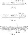
- FIGS. 3A to 3E are schematic cross-sectional views showing a method for fabricating a packaging substrate according to a second embodiment of the present disclosure
- FIGS. 4A and 4B are schematic cross-sectional views showing application of the packaging substrate of FIG. 2G ;
- FIG. 5 is a schematic cross-sectional view showing application of the packaging substrate of FIG. 3E ;
- FIGS. 6A to 6E are schematic cross-sectional views showing a method for fabricating a packaging substrate according to a third embodiment of the present disclosure, wherein FIG. 6E ′ shows another embodiment of FIG. 6E .
- FIGS. 2A to 2G are schematic cross-sectional views showing a method for fabricating a packaging substrate 2 according to a first embodiment of the present disclosure.
- a conductor layer 21 having a plurality of openings 210 is formed on a carrier 20 by a patterning process. Then, a first barrier layer 22 is formed on the carrier 20 and the conductor layer 21 and in the openings 210 of the conductor layer 21 .
- the carrier 20 is a substrate such as a copper foil substrate, and the conductor layer 21 is formed on the carrier 20 by electroplating.
- the conductor layer 21 and the first barrier layer 22 are made of different materials.
- the conductor layer 21 is a metal layer such as a copper layer
- the first barrier layer 22 is a metal layer, such as a nickel layer, a gold layer or a titanium layer.
- a second barrier layer 23 is further formed on the first barrier layer 22 .
- the first barrier layer 22 and the second barrier layer 23 are made of different materials.
- the second barrier layer 23 is a copper layer.
- a plurality of conductive bumps 24 are disposed on the first barrier layer 22 on the conductor layer 21 , and each of the conductive bumps 24 has a post body 240 disposed in a corresponding one of the openings 210 and a conductive pad 241 extending from and integrally formed with the post body 240 .
- the width d of the post body 240 is less than the width r of the conductive pad 241 .
- the conductive bumps 24 are formed by copper electroplating. Through the copper electroplating process, a first circuit layer 250 is further formed on the first barrier layer 22 on the carrier 20 .
- a plurality of conductive posts 26 are disposed on the conductive pads 241 , and a plurality of first conductive posts 251 are disposed on the first circuit layer 250 .
- the first conductive posts 251 and the first circuit layer 250 constitute a first circuit structure 25 on the carrier 20 .
- the conductive posts 26 and the first conductive posts 251 are formed by copper electroplating.
- a first insulating layer 27 is formed on the first barrier layer 22 , and encapsulates the conductive bumps 24 , the first circuit structure 25 and the conductive posts 26 .
- the first insulating layer 27 has a first surface 27 a bonded to the first barrier layer 22 and a second surface 27 b opposite to the first surface 27 a and exposing the conductive posts 26 and the first conductive posts 251 of the first circuit structure 25 .
- a surface of the first circuit layer 250 is flush with the first surface 27 a of the first insulating layer 27
- end surfaces of the conductive posts 26 and the first conductive posts 251 are flush with the second surface 27 b of the first insulating layer 27 .
- the second surface 27 b of the first insulating layer 27 is formed with a plurality of openings so as to expose the end surfaces of the conductive posts 26 and the first conductive posts 251 .
- the first insulating layer 27 is formed by lamination or molding and made of a molding compound, a dry film, an epoxy resin, polyimide or other photosensitive or non-photosensitive organic resin.
- a second circuit structure 28 is disposed on the second surface 27 b of the first insulating layer 27 . Then, a second insulating layer 29 is formed on the second surface 27 b of the first insulating layer 27 and encapsulates the second circuit structure 28 , and a portion of the second circuit structure 28 is exposed from the second insulating layer 29 .
- the second circuit structure 28 has a second circuit layer 280 formed on the second surface 27 b of the first insulating layer 27 and a plurality of second conductive posts 281 disposed on the second circuit layer 22 .
- the second circuit layer 280 is directly connected to the first conductive posts 251 and the conductive posts 26 .
- the second conductive posts 281 are copper posts, and end surfaces of the second conductive posts 281 are exposed from the second insulating layer 29 .
- the second insulating layer 29 is formed by lamination or molding and made of a molding compound, a dry film, an epoxy resin, polyimide or other photosensitive or non-photosensitive organic resin.
- the carrier 20 is removed to expose the conductor layer 21 and the first barrier layer 22 .
- a recessed portion 270 is formed on the first surface 27 a of the first insulating layer 27 , and the post bodies 240 of the conductive bumps 24 protrude from a bottom surface 270 a of the recessed portion 270 .
- the surface of the first circuit layer 250 is exposed from the first surface 27 a of the first insulating layer 27 .
- the entire conductor layer 21 and the entire first barrier layer 22 are removed by etching.
- the first barrier layer 22 is removed after the conductor layer 21 is removed, and the first barrier layer 22 serves as an etch stop layer during removal of the conductor layer 21 .
- the second barrier layer 23 serves as an etch stop layer during removal of the conductor layer 21 and the first barrier layer 22 and thereafter the entire second barrier layer 23 is removed.
- FIG. 2G a packaging substrate 2 is obtained.
- FIGS. 3A to 3E are schematic cross-sectional views showing a method for fabricating a packaging substrate 3 according to a second embodiment of the present disclosure.
- the second embodiment differs from the first embodiment in the configuration of the first barrier layer.
- a conductor layer 21 having a plurality of openings 210 is formed on a carrier 20 by a patterning process. Then, a first barrier layer 32 , 32 ′ is formed on a portion of the surface of the conductor layer 21 in the openings 210 and a portion of the surface of the carrier 20 by a patterning process.
- a plurality of conductive bumps 24 and a first circuit layer 250 are formed on the first barrier layer 32 , 32 ′ in a manner that the first barrier layer 32 bonded with the conductive bumps 24 is completely sandwiched between the conductive bumps 24 and the conductor layer 21 and the first barrier layer 32 ′ on the carrier 20 is completely sandwiched between the carrier 20 and the first circuit layer 250 .
- FIG. 3C the processes of FIGS. 2C to 2E are performed.
- the carrier 20 is removed to expose the first surface 27 a of the first insulating layer 27 , the conductor layer 21 and the first barrier layer 32 , 32 ′.
- a recessed portion 270 is formed on the first surface 27 a of the first insulating layer 27 and the post bodies 240 of the conductive bumps 24 protrude from a bottom surface 270 a of the recessed portion 270 .
- the first barrier layer 32 on the conductive bumps 24 is exposed from the recessed portion 270
- the first barrier layer 32 ′ on the first circuit layer 250 is exposed from the first surface 27 a of the first insulating layer 27 .
- the conductive bumps 24 are formed on the packaging substrate 2 , 3 . Therefore, compared with the conventional process for fabricating copper pillars on a semiconductor chip, the present disclosure reduces costs and facilitates production.
- the electroplating process for forming the conductive bumps 24 is performed inward (i.e., from an outer side of the packaging substrate 2 , 3 toward an inner side).
- the end surfaces of the post bodies 240 of the conductive bumps 24 have a uniform height, thus meeting the fine-pitch requirement. That is, the post bodies 240 of uniform height can be arranged in a grid array having a good coplanarity so as to ensure uniform joint stresses and avoid damage of the packaging substrate 2 , 3 or electronic elements 40 (to be described later) thereon.
- FIGS. 4A, 4B and 5 are schematic cross-sectional views showing electronic packages 4 , 4 ′, 5 formed by using the packaging substrates 2 , 3 according to the present disclosure.
- the packaging substrate 2 of FIG. 2G is used. At least an electronic element 40 is positioned corresponding to the recessed portion 270 and bonded to the post bodies 240 through a solder material 400 . As such, the electronic element 40 is electrically connected to the conductive bumps 24 . Further, another electronic element 40 ′ is bonded to the first circuit layer 250 through the solder material 400 .
- each of the electronic elements 40 , 40 ′ is an active element such as a semiconductor chip, a passive element, such as a resistor, a capacitor or an inductor, or a combination thereof.
- the electronic element 40 on the post bodies 240 is an active element
- the electronic element 40 ′ on the first circuit layer 250 is a passive element.
- a packaging layer 43 is formed on the first surface 27 a of the first insulating layer 27 to encapsulate the post bodies 240 , the electronic elements 40 , 40 ′ and the solder material 400 , and a plurality of solder balls 44 are disposed on the second surface 27 b of the first insulating layer 27 and electrically connected to the second conductive posts 281 so as to allow an electronic element (not shown) such as a circuit board to be disposed thereon.
- a circuit layer 41 is formed on the packaging layer 43 , and a plurality of conductors 42 are disposed in the packaging layer 43 for electrically connecting the circuit layer 41 and the first circuit layer 250 .
- the present disclosure dispenses with a conventional silicon interposer and hence reduces the overall height of the electronic package 4 so as to meet the thinning and cost reduction requirements.
- the electronic component 45 is bonded and electrically connected to the circuit layer 41 through a plurality of conductive elements 450 .
- the conductive elements 450 are solder balls, solder bumps or copper pillars, and the electronic component 45 is an active element, a passive element, a package element, or a combination thereof.
- the package element has a chip and an encapsulant encapsulating the chip.
- an encapsulant 46 is optionally formed on the packaging layer 43 to encapsulate the electronic component 45 .
- the packaging substrate 3 of FIG. 3E is used.
- An electronic element 40 is bonded to the first barrier layer 32 on the post bodies 240 through a solder material 400 .
- the electronic element 40 is electrically connected to the conductive bumps 24 .
- an underfill 50 is formed between the electronic element 40 and the recessed portions 270 to encapsulate the post bodies 240 , the first barrier layer 32 and the solder material 400 .
- another electronic element 40 ′ is bonded to the first barrier layer 32 ′ on the first circuit layer 250 through the solder material 400 .
- the first barrier layer 32 (e.g., a nickel layer) has a good bonding with the solder material 400 , thus strengthening the bonding between the electronic element 40 and the packaging substrate 3 .
- FIGS. 6A to 6E are schematic cross-sectional views showing a method for fabricating a packaging substrate 6 according to a third embodiment of the present disclosure.
- the third embodiment differs from the first and second embodiments in the omission of the first circuit structure 25 .
- FIGS. 6A and 6B the processes of FIGS. 3A and 3B are performed and the first circuit structure 25 is omitted.
- the process of FIG. 3C is performed and the second circuit layer 280 of the second circuit structure 28 is formed on the conductive posts 26 .
- the carrier 20 is removed to expose the first surface 27 a of the first insulating layer 27 , the conductor layer 21 and the first barrier layer 32 .
- the entire conductor layer 21 is removed. As such, the post bodies 240 of the conductive bumps 24 protrude from the first surface 27 a of the first insulating layer 27 .
- the processes of the first embodiment can be performed so as to obtain a packaging substrate 6 ′ of FIG. 6E ′.
- packaging substrate 6 , 6 ′ can be used to form an electronic package as shown in FIGS. 4A and 5 .
- the present disclosure further provides a packaging substrate 2 , 3 , 6 , 6 ′, which has: a first insulating layer 27 having a first surface 27 a and a second surface 27 b opposite to the first surface 27 a ; a plurality of conductive bumps 24 disposed on the first surface 27 a of the first insulating layer 27 , wherein each of the conductive bumps 24 has a post body 240 exposed from the first surface 27 a of the first insulating layer 27 and a conductive pad 241 embedded in the first insulating layer 27 and integrally formed with the post body 240 , the width d of the post body 240 being less than the width r of the conductive pad 241 ; and a plurality of conductive posts 26 disposed on the conductive pads 241 and embedded in the first insulating layer 27 , wherein end surfaces of the conductive posts 26 are exposed from the second surface 27 b of the first insulating layer 27 .
- the post bodies 240 protrude from the first surface 27 a of the first insulating layer 27 .
- At least a recessed portion 270 is formed on the first surface 27 a of the first insulating layer 27 in a manner that the conductive bumps 240 are located in the recessed portion 270 and the post bodies 240 of the conductive bumps 24 protrude from a bottom surface 270 a of the recessed portion 270 .
- the packaging substrate 2 , 3 further has a first circuit structure 25 disposed in the first insulating layer 27 and exposed from the first surface 27 a and the second surface 27 b of the first insulating layer 27 .
- the packaging substrate 2 , 3 , 6 , 6 ′ further has a second circuit structure 28 disposed on the second surface 27 b of the first insulating layer 27 , and a second insulating layer 29 formed on the second surface 27 b of the first insulating layer 27 to encapsulate the second circuit structure 28 , wherein portions of the second circuit structure 28 are exposed from the second insulating layer 29 .
- the packaging substrate 3 , 6 further has a barrier layer 32 formed on the post bodies 240 and exposed from the first surface 27 a of the first insulating layer 27 .
- the present disclosure reduces costs and facilitates production.
- an electroplating process for forming the conductive bumps is performed inward. As such, end surfaces of the post bodies of the conductive bumps have a uniform height, thus meeting the fine-pitch requirement.
Landscapes
- Engineering & Computer Science (AREA)
- Microelectronics & Electronic Packaging (AREA)
- Wire Bonding (AREA)
- Physics & Mathematics (AREA)
- Geometry (AREA)
- Structures For Mounting Electric Components On Printed Circuit Boards (AREA)
Abstract
Description
Claims (13)
Priority Applications (1)
| Application Number | Priority Date | Filing Date | Title |
|---|---|---|---|
| US15/961,973 US11031329B2 (en) | 2016-05-23 | 2018-04-25 | Method of fabricating packaging substrate |
Applications Claiming Priority (4)
| Application Number | Priority Date | Filing Date | Title |
|---|---|---|---|
| CN201610347780.6 | 2016-05-23 | ||
| CN201610347780.6A CN107424973B (en) | 2016-05-23 | 2016-05-23 | Package substrate and its manufacturing method |
| US15/402,362 US10002823B2 (en) | 2016-05-23 | 2017-01-10 | Packaging substrate and method of fabricating the same |
| US15/961,973 US11031329B2 (en) | 2016-05-23 | 2018-04-25 | Method of fabricating packaging substrate |
Related Parent Applications (1)
| Application Number | Title | Priority Date | Filing Date |
|---|---|---|---|
| US15/402,362 Division US10002823B2 (en) | 2016-05-23 | 2017-01-10 | Packaging substrate and method of fabricating the same |
Publications (2)
| Publication Number | Publication Date |
|---|---|
| US20180240748A1 US20180240748A1 (en) | 2018-08-23 |
| US11031329B2 true US11031329B2 (en) | 2021-06-08 |
Family
ID=60330936
Family Applications (3)
| Application Number | Title | Priority Date | Filing Date |
|---|---|---|---|
| US15/402,362 Active US10002823B2 (en) | 2016-05-23 | 2017-01-10 | Packaging substrate and method of fabricating the same |
| US15/961,970 Abandoned US20180240747A1 (en) | 2016-05-23 | 2018-04-25 | Packaging substrate and method of fabricating the same |
| US15/961,973 Active 2037-07-18 US11031329B2 (en) | 2016-05-23 | 2018-04-25 | Method of fabricating packaging substrate |
Family Applications Before (2)
| Application Number | Title | Priority Date | Filing Date |
|---|---|---|---|
| US15/402,362 Active US10002823B2 (en) | 2016-05-23 | 2017-01-10 | Packaging substrate and method of fabricating the same |
| US15/961,970 Abandoned US20180240747A1 (en) | 2016-05-23 | 2018-04-25 | Packaging substrate and method of fabricating the same |
Country Status (2)
| Country | Link |
|---|---|
| US (3) | US10002823B2 (en) |
| CN (1) | CN107424973B (en) |
Families Citing this family (14)
| Publication number | Priority date | Publication date | Assignee | Title |
|---|---|---|---|---|
| CN107424973B (en) * | 2016-05-23 | 2020-01-21 | 凤凰先驱股份有限公司 | Package substrate and its manufacturing method |
| CN106601627A (en) * | 2016-12-21 | 2017-04-26 | 江苏长电科技股份有限公司 | Process of first sealing then corrosion electro copper column conduction three-dimensional packaging structure |
| TWI631684B (en) * | 2017-09-05 | 2018-08-01 | Phoenix Pioneer Technology Co., Ltd. | Intermediary substrate and its preparation method |
| CN109427725B (en) * | 2017-09-05 | 2021-04-27 | 恒劲科技股份有限公司 | Interposer substrate and method of making the same |
| US10580715B2 (en) * | 2018-06-14 | 2020-03-03 | Texas Instruments Incorporated | Stress buffer layer in embedded package |
| CN111341743B (en) * | 2018-12-19 | 2024-04-16 | 株式会社村田制作所 | Electronic components |
| US11942334B2 (en) * | 2018-12-21 | 2024-03-26 | Intel Corporation | Microelectronic assemblies having conductive structures with different thicknesses |
| US11637060B2 (en) | 2019-07-18 | 2023-04-25 | Unimicron Technology Corp. | Wiring board and method of manufacturing the same |
| TWI728410B (en) * | 2019-07-18 | 2021-05-21 | 欣興電子股份有限公司 | Circuit board structure and manufacturing method thereof |
| KR102950444B1 (en) * | 2021-07-29 | 2026-04-09 | 삼성전기주식회사 | Printed circuit board |
| US12184237B2 (en) | 2021-11-01 | 2024-12-31 | Nxp Usa, Inc. | Surface-mount amplifier devices |
| US12040291B2 (en) | 2021-12-20 | 2024-07-16 | Nxp Usa, Inc. | Radio frequency packages containing multilevel power substrates and associated fabrication methods |
| TW202518607A (en) * | 2023-10-30 | 2025-05-01 | 強茂股份有限公司 | Manufacturing method of pre-molded packaging lead frame |
| CN118538680B (en) * | 2023-12-08 | 2026-01-06 | 芯爱科技(南京)有限公司 | Electronic Packages and Their Manufacturing Methods |
Citations (9)
| Publication number | Priority date | Publication date | Assignee | Title |
|---|---|---|---|---|
| US20100147573A1 (en) | 2007-09-06 | 2010-06-17 | Murata Manufacturing Co., Ltd. | Circuit substrate, circuit module and method for manufacturing the circuit substrate |
| US8058566B2 (en) * | 2007-06-29 | 2011-11-15 | Unimicron Technology Corp. | Packaging substrate structure and manufacturing method thereof |
| US8067695B2 (en) | 2008-12-12 | 2011-11-29 | Shinko Electric Industries Co., Ltd. | Wiring board and method of manufacturing the same |
| US20130250533A1 (en) | 2009-04-16 | 2013-09-26 | Shinko Electric Industries Co., Ltd. | Wiring substrate having columnar protruding part |
| US8686300B2 (en) | 2008-12-24 | 2014-04-01 | Ibiden Co., Ltd. | Printed wiring board and method for manufacturing the same |
| US20140239475A1 (en) * | 2013-02-27 | 2014-08-28 | Siliconware Precision Industries Co., Ltd. | Packaging substrate, semiconductor package and fabrication methods thereof |
| US20150068033A1 (en) * | 2011-07-08 | 2015-03-12 | Unimicron Technology Corporation | Method of fabricating packaging substrate |
| US9497864B2 (en) | 2013-03-26 | 2016-11-15 | Via Technologies, Inc. | Circuit substrate, semiconductor package and process for fabricating the same |
| US10002823B2 (en) * | 2016-05-23 | 2018-06-19 | Phoenix & Corporation | Packaging substrate and method of fabricating the same |
Family Cites Families (13)
| Publication number | Priority date | Publication date | Assignee | Title |
|---|---|---|---|---|
| US2823A (en) * | 1842-10-22 | Machine for cutting and grinding vegetables | ||
| JP2010537403A (en) * | 2007-08-15 | 2010-12-02 | テッセラ,インコーポレイテッド | Interconnecting elements having posts formed by plating |
| KR101067031B1 (en) * | 2009-07-31 | 2011-09-22 | 삼성전기주식회사 | Printed circuit board and manufacturing method thereof |
| KR101283821B1 (en) * | 2011-05-03 | 2013-07-08 | 엘지이노텍 주식회사 | The method for manufacturing the printed circuit board |
| JP5800674B2 (en) * | 2011-10-25 | 2015-10-28 | 日本特殊陶業株式会社 | Wiring board and manufacturing method thereof |
| US8802504B1 (en) * | 2013-03-14 | 2014-08-12 | Taiwan Semiconductor Manufacturing Company, Ltd. | 3D packages and methods for forming the same |
| TWI487444B (en) * | 2013-05-07 | 2015-06-01 | Unimicron Technology Corp | Carrier substrate and manufacturing method thereof |
| JP6158676B2 (en) * | 2013-10-15 | 2017-07-05 | 新光電気工業株式会社 | WIRING BOARD, SEMICONDUCTOR DEVICE, AND WIRING BOARD MANUFACTURING METHOD |
| TWI551199B (en) * | 2014-04-16 | 2016-09-21 | 矽品精密工業股份有限公司 | Substrate with electrical connection structure and preparation method thereof |
| TWI533771B (en) * | 2014-07-17 | 2016-05-11 | 矽品精密工業股份有限公司 | Coreless package substrate and its preparation method |
| CN105448856B (en) * | 2014-09-01 | 2018-04-06 | 碁鼎科技秦皇岛有限公司 | Chip-packaging structure, preparation method and chip package base plate |
| CN105470144B (en) * | 2014-09-09 | 2018-01-02 | 欣兴电子股份有限公司 | Coreless layer packaging substrate and manufacturing method thereof |
| TWI587463B (en) * | 2014-11-12 | 2017-06-11 | 矽品精密工業股份有限公司 | Semiconductor package structure and its manufacturing method |
-
2016
- 2016-05-23 CN CN201610347780.6A patent/CN107424973B/en active Active
-
2017
- 2017-01-10 US US15/402,362 patent/US10002823B2/en active Active
-
2018
- 2018-04-25 US US15/961,970 patent/US20180240747A1/en not_active Abandoned
- 2018-04-25 US US15/961,973 patent/US11031329B2/en active Active
Patent Citations (9)
| Publication number | Priority date | Publication date | Assignee | Title |
|---|---|---|---|---|
| US8058566B2 (en) * | 2007-06-29 | 2011-11-15 | Unimicron Technology Corp. | Packaging substrate structure and manufacturing method thereof |
| US20100147573A1 (en) | 2007-09-06 | 2010-06-17 | Murata Manufacturing Co., Ltd. | Circuit substrate, circuit module and method for manufacturing the circuit substrate |
| US8067695B2 (en) | 2008-12-12 | 2011-11-29 | Shinko Electric Industries Co., Ltd. | Wiring board and method of manufacturing the same |
| US8686300B2 (en) | 2008-12-24 | 2014-04-01 | Ibiden Co., Ltd. | Printed wiring board and method for manufacturing the same |
| US20130250533A1 (en) | 2009-04-16 | 2013-09-26 | Shinko Electric Industries Co., Ltd. | Wiring substrate having columnar protruding part |
| US20150068033A1 (en) * | 2011-07-08 | 2015-03-12 | Unimicron Technology Corporation | Method of fabricating packaging substrate |
| US20140239475A1 (en) * | 2013-02-27 | 2014-08-28 | Siliconware Precision Industries Co., Ltd. | Packaging substrate, semiconductor package and fabrication methods thereof |
| US9497864B2 (en) | 2013-03-26 | 2016-11-15 | Via Technologies, Inc. | Circuit substrate, semiconductor package and process for fabricating the same |
| US10002823B2 (en) * | 2016-05-23 | 2018-06-19 | Phoenix & Corporation | Packaging substrate and method of fabricating the same |
Non-Patent Citations (1)
| Title |
|---|
| Non-Final Office Action for U.S. Appl. No. 15/402,362 dated Sep. 8, 2017, 31 pages. |
Also Published As
| Publication number | Publication date |
|---|---|
| US20170338174A1 (en) | 2017-11-23 |
| US20180240747A1 (en) | 2018-08-23 |
| CN107424973B (en) | 2020-01-21 |
| CN107424973A (en) | 2017-12-01 |
| US10002823B2 (en) | 2018-06-19 |
| US20180240748A1 (en) | 2018-08-23 |
Similar Documents
| Publication | Publication Date | Title |
|---|---|---|
| US11031329B2 (en) | Method of fabricating packaging substrate | |
| US11908835B2 (en) | Semiconductor structure and manufacturing method thereof | |
| US11289346B2 (en) | Method for fabricating electronic package | |
| US10796970B2 (en) | Method for fabricating electronic package | |
| US9412714B2 (en) | Wire bond support structure and microelectronic package including wire bonds therefrom | |
| US12255182B2 (en) | Electronic package and manufacturing method thereof | |
| US10199320B2 (en) | Method of fabricating electronic package | |
| US20150325556A1 (en) | Package structure and method for fabricating the same | |
| US20190043819A1 (en) | Electronic package having redistribution structure | |
| US9754982B2 (en) | Packaging module and substrate structure thereof | |
| US9607963B2 (en) | Semiconductor device and fabrication method thereof | |
| US9907186B1 (en) | Electronic package structure and method for fabricating the same | |
| US20150325516A1 (en) | Coreless packaging substrate, pop structure, and methods for fabricating the same | |
| US10600708B2 (en) | Electronic package and method for fabricating the same | |
| CN108281408A (en) | Semiconductor chip package and stack package | |
| CN110581107A (en) | Semiconductor package and manufacturing method thereof | |
| US12412820B2 (en) | Electronic package and manufacturing method thereof | |
| US9601403B2 (en) | Electronic package and fabrication method thereof | |
| US20160104652A1 (en) | Package structure and method of fabricating the same | |
| TWI567843B (en) | Package substrate and its preparation method | |
| US20250336739A1 (en) | Electronic package and manufacturing method thereof | |
| TWM546005U (en) | Package structure | |
| CN107768320A (en) | Electronic package and manufacturing method thereof |
Legal Events
| Date | Code | Title | Description |
|---|---|---|---|
| AS | Assignment |
Owner name: PHOENIX & CORPORATION, CAYMAN ISLANDS Free format text: ASSIGNMENT OF ASSIGNORS INTEREST;ASSIGNORS:HU, CHU-CHIN;HSU, SHIH-PING;HSU, CHE-WEI;AND OTHERS;SIGNING DATES FROM 20161117 TO 20161121;REEL/FRAME:045629/0351 |
|
| FEPP | Fee payment procedure |
Free format text: ENTITY STATUS SET TO UNDISCOUNTED (ORIGINAL EVENT CODE: BIG.); ENTITY STATUS OF PATENT OWNER: SMALL ENTITY |
|
| FEPP | Fee payment procedure |
Free format text: ENTITY STATUS SET TO SMALL (ORIGINAL EVENT CODE: SMAL); ENTITY STATUS OF PATENT OWNER: SMALL ENTITY |
|
| STPP | Information on status: patent application and granting procedure in general |
Free format text: DOCKETED NEW CASE - READY FOR EXAMINATION |
|
| STPP | Information on status: patent application and granting procedure in general |
Free format text: NON FINAL ACTION MAILED |
|
| AS | Assignment |
Owner name: PHOENIX PIONEER TECHNOLOGY CO., LTD., TAIWAN Free format text: ASSIGNMENT OF ASSIGNORS INTEREST;ASSIGNOR:PHOENIX & CORPORATION;REEL/FRAME:052990/0860 Effective date: 20200618 |
|
| STPP | Information on status: patent application and granting procedure in general |
Free format text: RESPONSE TO NON-FINAL OFFICE ACTION ENTERED AND FORWARDED TO EXAMINER |
|
| STPP | Information on status: patent application and granting procedure in general |
Free format text: NON FINAL ACTION MAILED |
|
| STPP | Information on status: patent application and granting procedure in general |
Free format text: RESPONSE TO NON-FINAL OFFICE ACTION ENTERED AND FORWARDED TO EXAMINER |
|
| STPP | Information on status: patent application and granting procedure in general |
Free format text: NOTICE OF ALLOWANCE MAILED -- APPLICATION RECEIVED IN OFFICE OF PUBLICATIONS |
|
| STPP | Information on status: patent application and granting procedure in general |
Free format text: PUBLICATIONS -- ISSUE FEE PAYMENT RECEIVED |
|
| STPP | Information on status: patent application and granting procedure in general |
Free format text: PUBLICATIONS -- ISSUE FEE PAYMENT VERIFIED |
|
| STCF | Information on status: patent grant |
Free format text: PATENTED CASE |
|
| MAFP | Maintenance fee payment |
Free format text: PAYMENT OF MAINTENANCE FEE, 4TH YR, SMALL ENTITY (ORIGINAL EVENT CODE: M2551); ENTITY STATUS OF PATENT OWNER: SMALL ENTITY Year of fee payment: 4 |