TWI875219B - Light-emitting device - Google Patents
Light-emitting device Download PDFInfo
- Publication number
- TWI875219B TWI875219B TW112137373A TW112137373A TWI875219B TW I875219 B TWI875219 B TW I875219B TW 112137373 A TW112137373 A TW 112137373A TW 112137373 A TW112137373 A TW 112137373A TW I875219 B TWI875219 B TW I875219B
- Authority
- TW
- Taiwan
- Prior art keywords
- light
- reflective layer
- layer
- electrode
- emitting device
- Prior art date
Links
Images




Landscapes
- Led Devices (AREA)
Abstract
Description
本揭露是關於一種發光裝置,特別是關於一種包括反射層的發光裝置。The present disclosure relates to a light emitting device, and more particularly to a light emitting device including a reflective layer.
發光二極體(light-emitting diodes, LEDs)是一種發光裝置,可在施加電壓時發出光線。氮化物發光二極體常作為產生藍光或綠光的半導體光學元件。在考量化合物的晶格匹配性的情況下,一般會在藍寶石基板上成長氮化物半導體材料,再形成電極結構以形成氮化物發光二極體。然而藍寶石基板硬度高、熱導率且電導率低,不僅具有靜電問題也是限制原有正裝LED晶片散熱的主要因素;此外,原有正裝LED結構中,電極會遮掉一部分光而降低發光效率。因此,逐漸發展出LED的覆晶(flip chip)結構。Light-emitting diodes (LEDs) are light-emitting devices that emit light when voltage is applied. Nitride LEDs are often used as semiconductor optical elements that produce blue or green light. Taking into account the lattice matching of the compound, nitride semiconductor materials are generally grown on a sapphire substrate, and then an electrode structure is formed to form a nitride LED. However, the sapphire substrate has high hardness, low thermal conductivity and low electrical conductivity. It not only has electrostatic problems, but is also the main factor limiting the heat dissipation of the original regular LED chip; in addition, in the original regular LED structure, the electrode will block part of the light and reduce the luminous efficiency. Therefore, the flip chip structure of LED has gradually developed.
目前常見的LED覆晶技術係將製備完成之LED晶片反轉後焊接至封裝基板上,由於晶片反轉,熱傳導路徑可直接由半導體層傳導至封裝基板,可避免藍寶石基板散熱不佳之問題;另外,傳統上,在覆晶技術期間,通過一系列製程,形成陣列排列的LED晶片採用一選取頭(pick-up head)對應一晶片的方式,自一載板執行挑選或轉移至另一載板。然而,傳統製程可能遇到一些難題,例如,微發光二極體晶粒的邊長尺寸小於選取頭的最小尺寸極限,導致無法有效拾取LED晶片;又例如,晶粒尺寸的微縮化,代表同尺寸晶圓所能形成的晶粒數量將巨量增加,傳統製程中以一對一拾取的方式勢必無法滿足巨量轉移LED晶片的需求,導致發光二極體的產率降低。The most common LED flip chip technology currently is to flip the prepared LED chip and then solder it to the package substrate. Since the chip is flipped, the heat conduction path can be directly conducted from the semiconductor layer to the package substrate, which can avoid the problem of poor heat dissipation of the sapphire substrate. In addition, traditionally, during the flip chip technology period, a series of processes are used to form an array of LED chips, and a pick-up head is used to select or transfer one chip from one carrier to another. However, the traditional process may encounter some difficulties. For example, the side length of the micro-LED die is smaller than the minimum size limit of the selection head, resulting in the inability to effectively pick up the LED chip. For example, the miniaturization of the die size means that the number of die that can be formed on the same size wafer will increase dramatically. The one-to-one picking method in the traditional process will inevitably be unable to meet the demand for mass transfer of LED chips, resulting in a decrease in the yield of LEDs.
在巨量轉移(mass transfer)LED晶片技術的演進過程中,為了滿足高效率需求並達到較高的產能,利用選擇性的雷射剝離(selective laser lift-off, selective LLO)技術取代傳統製程,然而雖然現有的選擇性的雷射剝離技術大致可符合需求,但並非在所有方面皆令人滿意。因此,仍需要針對選擇性的雷射剝離技術及發光裝置的結構與其形成方法進行改良,以製造出符合產品需求的發光裝置。In the evolution of mass transfer LED chip technology, in order to meet the high efficiency requirements and achieve higher production capacity, selective laser lift-off (selective LLO) technology is used to replace the traditional process. However, although the existing selective laser lift-off technology can generally meet the requirements, it is not satisfactory in all aspects. Therefore, there is still a need to improve the selective laser lift-off technology and the structure and formation method of the light-emitting device to manufacture a light-emitting device that meets product requirements.
根據本揭露的一些實施例,提供一種發光裝置。發光裝置包括:第一型發光二極體晶粒,包含半導體層及第一電極,第一電極位於第一型發光二極體晶粒的前側並與半導體層電性連接,其中第一型發光二極體晶粒具有出射光,自半導體層內部發出;第一反射層及第二反射層,依序堆疊於第一型發光二極體晶粒的前側,且第一反射層及第二反射層位於半導體層及第一電極之間,其中第一反射層用以反射來自第一型發光二極體晶粒內部的出射光,第二反射層用以反射來自外部的雷射光,且雷射光的波長小於420nm。According to some embodiments of the present disclosure, a light-emitting device is provided. The light-emitting device includes: a first-type light-emitting diode die, including a semiconductor layer and a first electrode, the first electrode is located at the front side of the first-type light-emitting diode die and electrically connected to the semiconductor layer, wherein the first-type light-emitting diode die has an output light, which is emitted from the inside of the semiconductor layer; a first reflective layer and a second reflective layer, which are sequentially stacked at the front side of the first-type light-emitting diode die, and the first reflective layer and the second reflective layer are located between the semiconductor layer and the first electrode, wherein the first reflective layer is used to reflect the output light from the inside of the first-type light-emitting diode die, and the second reflective layer is used to reflect the laser light from the outside, and the wavelength of the laser light is less than 420nm.
以下實施例中參照所附圖式提供詳細敘述。The following embodiments provide a detailed description with reference to the accompanying drawings.
以下說明本揭露實施例之發光裝置及其形成方法。然而,應能理解本揭露實施例提供許多合適的發明概念而可實施於廣泛的各種特定背景。所揭示的特定實施例僅用於說明以特定方法製作及使用本發明,而並非用以侷限本發明的範圍。再者,在本揭露實施例之圖式及說明內容中係使用相同的標號來表示相同或相似的部件。The following describes the light emitting device and its forming method of the disclosed embodiment. However, it should be understood that the disclosed embodiment provides many suitable inventive concepts and can be implemented in a wide variety of specific contexts. The disclosed specific embodiment is only used to illustrate the manufacture and use of the invention in a specific method, and is not used to limit the scope of the invention. Furthermore, the same reference numerals are used in the drawings and descriptions of the disclosed embodiment to represent the same or similar components.
此外,本揭露提供了許多的實施例或範例,用於實施所提供的標的物之不同元件。各元件和其配置的具體範例描述如下,以簡化本發明實施例之說明。當然,這些僅僅是範例,並非用以限定本發明實施例。舉例而言,敘述中若提及第一元件形成在第二元件之上,可能包含第一和第二元件直接接觸的實施例,也可能包含額外的元件形成在第一和第二元件之間,使得它們不直接接觸的實施例。In addition, the present disclosure provides many embodiments or examples for implementing different elements of the subject matter provided. Specific examples of each element and its configuration are described below to simplify the description of the embodiments of the present invention. Of course, these are merely examples and are not intended to limit the embodiments of the present invention. For example, if the description refers to a first element formed on a second element, it may include an embodiment in which the first and second elements are directly in contact, and it may also include an embodiment in which an additional element is formed between the first and second elements so that they are not in direct contact.
再者,其中可能用到與空間相對用詞,例如「在……之下」、「下方」、「較低的」、「上方」、「較高的」等類似用詞,是為了便於描述圖式中一個(些)部件或特徵與另一個(些)部件或特徵之間的關係。空間相對用詞用以包括使用中或操作中的裝置之不同方位,以及圖式中所描述的方位。當裝置被轉向不同方位時(旋轉90度或其他方位),其中所使用的空間相對形容詞也將依轉向後的方位來解釋。Furthermore, spatially relative terms such as "under", "below", "lower", "above", "higher" and the like may be used to facilitate describing the relationship between one component or feature and another component or feature in the drawings. Spatially relative terms are used to include different orientations of the device in use or operation, as well as the orientations described in the drawings. When the device is rotated 90 degrees or in other orientations, the spatially relative adjectives used will also be interpreted based on the rotated orientation.
根據本揭露的一些實施例,發光裝置包括第一反射層與第二反射層,第一反射層設置在發光二極體晶粒上,第二反射層設置在第一反射層上。現有發光裝置所使用的巨量轉移製程中,當使用選擇性的雷射剝離 (selective LLO) 技術時,雷射的高溫可能會擊傷發光二極體晶粒,因此降低發光二極體晶粒的良率,影響發光裝置的性能。為解決上述問題,本揭露實施例所提供的發光裝置中,透過在發光二極體晶粒上設置雙反射層,不但可增進發光二極體晶粒的外部量子效率(external quantum efficiency, EQE),也可以反射選擇性的雷射剝離技術(selective LLO)所使用的雷射,防止造成發光二極體晶粒細微的損壞。According to some embodiments of the present disclosure, the light emitting device includes a first reflective layer and a second reflective layer, wherein the first reflective layer is disposed on a light emitting diode die, and the second reflective layer is disposed on the first reflective layer. In the mass transfer process used in existing light emitting devices, when using selective laser lift-off (selective LLO) technology, the high temperature of the laser may damage the light emitting diode die, thereby reducing the yield of the light emitting diode die and affecting the performance of the light emitting device. To solve the above problems, in the light-emitting device provided by the embodiment of the present disclosure, a double reflection layer is provided on the LED grain, which can not only improve the external quantum efficiency (EQE) of the LED grain, but also reflect the laser used in the selective laser lift-off technology (selective LLO) to prevent the LED grain from being slightly damaged.
第1圖繪示出本揭露實施例,發光裝置10的剖面示意圖。在第1圖中,發光裝置10包括基板102與多個發光二極體晶粒104間隔設置在基板102上。為簡化圖式,圖中僅繪示出三個發光二極體晶粒104,但本揭露不以此為限。每個發光二極體晶粒104具有第一電極112a(例如正極)與第二電極112b(例如負極)。在一些實施例中,第一電極112a為負極,第二電極112b為正極。第一電極112a與第二電極112b設置在發光二極體晶粒104遠離基板102同一側(可以稱為前側)。在一些實施例中,基板102可以為藍寶石基板、矽基板、碳化矽基板或陶瓷基板。發光二極體晶粒104可以是發出藍光、紅光或綠光的發光二極體晶片。FIG. 1 shows a cross-sectional schematic diagram of a light-
第2圖是繪示出第1圖的發光二極體晶粒104的詳細剖面結構。在第2圖中,在發光二極體晶粒104上設置有第一反射層106,且在第一反射層106上更設置有第二反射層108。第一反射層106用以反射源自發光二極體晶粒104內部的出射光,增加外部量子效率(EQE)。第二反射層108用以反射隨後在批量轉移發光二極體晶粒104的過程中所使用選擇性雷射剝離技術(selective LLO)的外部雷射,防止發光二極體晶粒細微的損壞。在一些實施例中,第一電極112a與第二電極112b穿過第二反射層108,與發光二極體晶粒104電性接觸,如圖中所示。隨後將更詳細描述形成第一反射層106與第二反射層108的製程。FIG. 2 shows a detailed cross-sectional structure of the
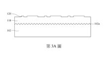
第3A至3D圖是根據本揭露的各種實施例,繪示出形成發光二極體晶粒104的過程中各個中間階段的剖面圖。參照第3A圖,在半導體基板102上沉積磊晶半導體層118。在一些實施例中,在沉積磊晶半導體層118之前,可以先對半導體基板102實施粗化製程,形成一周期性粗化表面102a。在一些實施例中,使用圖案化基板(Patterened Sapphire Substrate, PSS)技術,形成圖案化的基板,以增加光萃取效率。舉例來說,可以形成圖案化基板通過微影製程和蝕刻製程。在微影製程中,首先通過例如旋轉塗佈將光阻層(未示出)施加到半導體基板102上。接著,根據圖案遮罩對光阻層曝光,並進行顯影以在光阻層中形成週期性的圖案。具有週期性圖案的光阻層可以作為蝕刻遮罩以圖案化半導體基板102。然後使用圖案化的光阻層保護半導體基板102的一部份表面,而蝕刻製程在未受保護的區域中形成凹入半導體基板102表面的凹洞 ,因此留下周期性粗化表面102a。最後移除光阻層,例如通過灰化。在一些實施例中,形成周期性粗化表面102a使用乾蝕刻例如反應離子蝕刻(reactive ion etching, RIE)、濕蝕刻或其組合。FIGS. 3A to 3D are cross-sectional views of various intermediate stages in the process of forming a light-emitting
應注意的是,此處的粗化製程是可選的,可以不進行,或是在後續製程中再對發光二極體晶粒104進行粗化(詳述於後)。在一些實施例中,磊晶半導體層118包括第一型半導體層、發光層以及第二型半導體層依序形成於基板102上。舉例來說,第一型半導體層與第二型半導體層可以為不同類型的半導體材料,例如第一型半導體層為具有n型導電性質之氮化鎵(n-GaN),第二型半導體層為具有p型導電性質之氮化鎵(p-GaN),亦可互換。可使用其他III-V族化合物,例如:氮化銦(InN)、氮化鋁(AlN)、氮化銦鎵(InxGa(1-x)N)、氮化鋁鎵(AlxGa(1-x)N)、或氮化鋁銦鎵(AlxInyGa(1-x-y)N)等,其中0<x ≤1、0< y ≤1且0≤ x+y ≤1。發光層可以具有半導體材料所構成的多量子井結構(Multiple Quantum Well, MQW)。發光層可以包括其他合適的發光材料,但不限於此。在一實施例中,磊晶半導體層118之形成方法可以包括磊晶成長製程,例如化學氣相沉積(CVD)、金屬有機化學氣相沉積(MOCVD)、分子束磊晶(MBE)、氫化物氣相磊晶(HVPE)、液相磊晶(LPE)或其他適合的化學氣相沉積方法。It should be noted that the roughening process here is optional and may not be performed, or the light-emitting
再次參照第3A圖,接著,在磊晶半導體層118上形成圖案化的平台結構(mesa structure)120,通過圖案化製程,定義出接下來要形成的元件的範圍。上述圖案化製程可以包括微影及蝕刻製程,類似於前述的圖案化製程,在此不與贅述。Referring again to FIG. 3A , a patterned
參照第3B圖,在平台結構120上形成第一反射層106。第一反射層106對發光二極體晶粒104的出射光具有具高反射率,例如大於90%,用以反射發光二極體晶粒104的出射光,增加外部量子效率(EQE)。在一些實施例中,第一反射層106可以為布拉格反射層,在一實施例中,布拉格反射層可以包括兩種具有不同折射率(refractive index)之材料層交替排列組合而成之週期性結構,或有效折射率具有週期性變化特性之介電質波導(dielectric waveguide)。在一實施例中,布拉格反射層的材料可以包括絕緣體。舉例而言,布拉格反射鏡的材料可包括二氧化矽(SiO
2)、二氧化鈦(TiO
2)、氧化鉭(Ta
2O
5)、氧化鋁(Al
2O
3)或氮化矽(Si
3N
4),但不限於此。各層的厚度與入射光的波長有關,當各層的折射率與光學厚度之乘積等於入射光之波長的四分之一時,因入射光與反射光的光程差恰好為入射光之波長的整數倍(nλ, n=1,2,3…),則產生建設性干涉,無法穿透布拉格反射層,藉由上述原理及材料特性,反射發光二極體晶粒104出射光,增加外部量子效率(EQE)。在一實施例中,布拉格反射層的層數越高,光反射越明顯。在一些實施例中,第一反射層106的厚度可控制在0.1µm~4µm的範圍,例如0.6µm~2µm。
Referring to FIG. 3B , a first
接著,形成第二反射層108在第一反射層106上。第二反射層108對於隨後在批量轉移發光二極體晶粒104的過程中所使用選擇性雷射剝離技術(selective LLO)的雷射具有高反射率,例如大於90%,因此第二反射層108可以反射隨後所使用選擇性雷射剝離技術(selective LLO)的雷射,防止發光二極體晶粒微損壞。在一些實施例中,第二反射層108可以為布拉格反射層,使用與前述第一反射層106為布拉格反射層不同的厚度。在一些實施例中,第二反射層108的材料可以類似於第一反射層106為布拉格反射層的材料。在一些實施例中,第二反射層108的材料可以完全相同於第一反射層106為布拉格反射層的材料,降低製程難度。在一些實施例中,第二反射層108的材料可以不同於第一反射層106為布拉格反射層的材料,依據發光裝置的設計需求。在一些實施例中,第二反射層108的層數越高,反射效果越好,提升發光裝置的良率。在一些實施例中,第二反射層108的厚度可控制在0.1µm~4µm的範圍,例如0.6µm~2µm。在一些實施例中,第二反射層108的厚度小於第一反射層106的厚度。Next, a second
然後,對第一反射層106以及第二反射層108圖案化,形成穿過第一反射層106以及第二反射層108的凹洞111,露出磊晶半導體層118的部分,如第3B圖所示。所述凹洞111將於後續用來形成發光二極體晶粒的電極。圖案化製程可以使用類似於前述的圖案化製程,在此不予贅述。Then, the first
參照第3C圖,蝕刻磊晶半導體層118以形成各個分隔設置的發光二極體晶粒104。蝕刻製程可以包括乾蝕刻例如反應離子蝕刻( RIE)、濕蝕刻或其組合。3C, the
參照第3D圖,形成穿過第一反射層106以及第二反射層108的第一電極112a與第二電極112b並與發光二極體晶粒104實體接觸。在一些實施例中,第一電極112a與第二電極112b的材料可以包括金屬或金屬合金。舉例而言,第一電極112a與第二電極112b金屬材料可以包括:銅(Cu)、鋁(Al)、銦(In)、錫(Sn)、金(Au)、鉑(Pt)、鋅(Zn)、銀(Ag)、鈦(Ti)、鎳(Ni)或其組合,但不限於此。在一些實施例中,形成第一電極112a與第二電極112b可以使用化學氣相沉積(CVD),包括低壓化學氣相沉積(LPCVD)和電漿化學氣相沉積(PECVD)、物理氣相沉積(PVD)、原子層沉積(ALD)或其他合適的沉積製程。隨後,使用微影和蝕刻製程圖案化電極層,如第3D圖所示。舉例來說,可以使用類似於前述的圖案化製程,在此不予贅述。Referring to FIG. 3D , a
參照第4A-4D圖,根據本揭露的各種實施例,繪示出形成具有不同類型及或不同輪廓的反射層的剖面圖。在第4A圖中,在一些實施例中,第一反射層106與第二反射層108皆為布拉格反射層,第一反射層106可以反射發光二極體晶粒104向前側(具有電極的一側)發出的光,增加外部量子效率(EQE)。第二反射層108可以反射隨後在巨量轉移發光二極體晶粒104的過程中所使用選擇性雷射剝離技術(selective LLO)的雷射,防止發光二極體晶粒微損壞。如第4A、4C及4D圖所示,在一些實施例中,第二反射層108的側壁與發光二極體晶粒104的外露側壁對齊。此外,如第4B-4C圖所示,發光二極體晶粒104的前側的邊緣可具有低於平台結構120的一開口,當第一反射層106與第二反射層108形成於發光二極體晶粒104的前側時,第一反射層106以及第二反射層108可以向基板延伸,從而填入所述開口以覆蓋發光二極體晶粒104的大部分側壁。第一反射層106的延伸部分可以反射發光二極體晶粒104向左右兩側發出的光,進而增加外部量子效率(EQE) ,第二反射層108的延伸部分可以反射隨後在批量轉移發光二極體晶粒104的過程中所使用選擇性雷射剝離技術(selective LLO)的雷射。如第4B圖所示,在一些實施例中,第一反射層106與第二反射層108可填滿所述開口,使第二反射層108的側壁與發光二極體晶粒104的外露側壁對齊,此可保留較厚的第一反射層106以及第二反射層108,從而增加外部量子效率(EQE),並且可以加強反射隨後在批量轉移所使用選擇性雷射剝離技術(selective LLO)的雷射。或者,如第4C圖所示,在一些實施例中,第一反射層106與第二反射層108可不填滿所述開口,使第二反射層108的側壁內縮於發光二極體晶粒104的側壁,此可減少製程複雜度,從而毋須使用額外步驟以對齊第二反射層108的側壁與發光二極體晶粒104的外露側壁。Referring to FIGS. 4A-4D , according to various embodiments of the present disclosure, cross-sectional views of reflective layers having different types and/or different profiles are shown. In FIG. 4A , in some embodiments, the first
此外,在另一些實施例中,第一反射層106可以為金屬層,用以反射發光二極體晶粒104的出射光,增加外部量子效率(EQE),如第4D圖所示。在一些實施例中,第一反射層106的材料包括金屬,例如銀(Ag)、鋁(Al)、金(Au)。在一些實施例中,第一反射層106可以具有厚度在約 1000Å 至約 10000Å的範圍。可以形成第一反射層106通過使用化學氣相沉積(CVD),包括低壓化學氣相沉積(LPCVD)和電漿化學氣相沉積(PECVD)、物理氣相沉積(PVD)、原子層沉積(ALD)或其他合適的沉積製程。特別注意的是,當第一反射層106為金屬層,可於形成磊晶半導體層118後,直接沉積金屬層,然後再進行蝕刻金屬層與磊晶半導體層118以形成平台結構120以及位於平台結構120上表面的圖案化第一反射層106。接著,形成圖案化的第二反射層108在第一反射層106上,圖案化製程可以使用類似於前述的圖案化製程。圖案化的第二反射層108露出第一反射層106的一部分以及磊晶半導體層118的一部分。 最後,形成第一電極112a接觸磊晶半導體層118,形成第二電極112b接觸第一反射層106,如第4D圖所示。為了簡化圖式,實施例的製程剖面圖僅列舉一種發光二極體晶粒104和第一反射層106的配置方式,但可以是4A-4D任何一種。In addition, in other embodiments, the first
參照第5圖,根據本揭露的一些實施例,第一反射層106側向地包覆發光層119。第一反射層106的深入側壁的最底端可以低於或等於發光層119的底表面,可以反射發光層119向左右兩側發出的光,進而增加發光二極體晶粒104的外部量子效率(EQE)。5 , according to some embodiments of the present disclosure, the first
參照第6圖,根據本揭露的其他實施例,在沉積第一反射層之前及/或沉積第二反射層之後,可視需要形成阻障膜110a及/或110b在發光二極體晶粒104上及/或在第二反射層108上。阻障膜110a、110b用來覆蓋第一反射層106、第二反射層108的表面,除了可以保護第一反射層106、第二反射層108不受外界物質例如水氣或氧氣的損壞影響,也可以填補沉積反射層時造成的缺陷,防止漏電流,增加可靠性(reliability)。在一些實施例中,阻障膜110a、 110b可各自包括無機材料,例如金屬氧化物(如SiO
2、Al
2O
3等)或金屬氮化物(如Si
3N
3等)。在一些實施例中,阻障膜110a、110b可以是多層阻障膜,以塗佈或貼膜方式設置於第一反射層106及/或第二反射層108的表面。在一些實施例中,阻障膜110a、110b的厚度大於10nm,小於500nm。
Referring to FIG. 6 , according to other embodiments of the present disclosure, before depositing the first reflective layer and/or after depositing the second reflective layer, a
第7、8、9、10、11、12、13、14、15和16圖是根據本揭露的一些實施例,繪示出巨量轉移發光二極體晶粒104的過程中各個中間階段的剖面圖。FIGS. 7, 8, 9, 10, 11, 12, 13, 14, 15 and 16 are cross-sectional views showing various intermediate stages in the process of mass transferring LED die 104 according to some embodiments of the present disclosure.
參照第7圖,首先,提供載板202,且載板202具上有第一黏著層114(亦可以稱為膠體)。在一些實施例中,載板202的材料可包括塑膠基板、玻璃基板、矽基板或藍寶石基板、或其他合適的材料,但不限於此。在一些實施例中,第一黏著層114可以為UV膠,與之後所使用的雷射反應。在一些實施例中,第一黏著層114吸收所使用的雷射後會裂解,使得發光二極體晶粒104自第一黏著層114剝離。在一些實施例中,所使用的雷射的波長小於420nm舉例來說,波長為248、260、280、355nm等,但不限於此。Referring to FIG. 7 , first, a
在一些實施例中,可以通過旋轉塗佈沉積第一黏著層114於載板202上。接著,將第1圖的半導體裝置10的第一電極112a與第二電極112b接合至載板202上的第一黏著層114。在一些實施例中,第一黏著層114被擠入發光二極體晶粒104之間的間隙,附著在發光二極體晶粒104的部分側壁,包覆第一電極112a與第二電極112b,但未直接接觸基板102,如第7圖所示。在一些實施例中,第一黏著層114覆蓋發光二極體晶粒104大於80%的表面。在其他實施例中,第一黏著層114可以附著在發光二極體晶粒104的周圍,直接接觸基板102(未示出)。In some embodiments, the first
參照第8圖,通過完全雷射剝離(fully LLO)製程113移除基板102,以將所有發光二極體晶粒104轉移至載板202。在一些實施例中,從基板102面施加完全雷射剝離(fully LLO) 製程113,以移除基板102。在一些實施例中,完全雷射剝離(fully LLO) 製程113所使用的雷射的波長在420nm以下,舉例來說,波長為248、260、280、355nm等,但不限於此。在一些實施例中,發光二極體晶粒104的材料可以完全吸收全雷射剝離技術(fully LLO)所使用的雷射,而避免雷射對發光二極體晶粒104造成的擊傷,舉例來說,在發光二極體晶粒104包括III-V族化合物(例如氮化鎵)的實施例中,III-V族化合物可以在與基板102的界面完全吸收雷射,防止雷射擊傷發光二極體晶粒104,提升發光裝置的良率。8, the
參照第9圖,在一些實施例中,由於基板102具有圖案化的週期性表面102a,因此發光二極體晶粒104在與基板102的交界處亦具有週期性粗化表面104a。在雷射剝離製程之後,可以露出發光二極體晶粒104的週期性粗化表面104a,以增加發光二極體晶粒104的出光效率。9 , in some embodiments, since the
參照第10圖,在另一些實施例中,也可在移除基板102之後,視需要通過一粗化製程117在發光二極體晶粒104的露出表面上形成粗化表面117a,增加發光二極體晶粒104的出光效率。在一些實施例中,粗化表面117a可以包括半導體材料及/或高分子聚合物。舉例來說,可以在發光二極體晶粒104的週期性粗化表面上可選地形成透光層(未示出)。透光層可以包括高分子聚合物例如矽膠或樹脂,可以形成通過封膠(molding)、灌膠(glue-filling)或其他合適的製程。接著對透光層執行粗化製程117,以形成週期性的粗化表面117a,通過例如噴砂或表面蝕刻等方式。在一些實施例中,粗化表面117a的表面粗糙度可以為0.1µm~3µm的範圍,例如0.2µm~2µm,但不限於此。Referring to FIG. 10 , in other embodiments, after removing the
參照第11圖,形成發光裝置20。接續第9圖,蝕刻發光二極體晶粒104側壁間的第一黏著層114,露出載板202的上表面,分開每個發光二極體晶粒104,以利後續執行選擇性轉移發光二極體晶粒104的製程,減少因第一黏著層114殘留在每個發光二極體晶粒104之間,而造成選擇性轉移的困難。蝕刻製程可以包括乾蝕刻例如反應離子蝕刻( RIE)、濕蝕刻或其組合。Referring to FIG. 11 , a
參照第12圖,接續第11圖,提供第二載板302,且第二載板302上具有第二黏著層115。在一些實施例中,第二載板302的材料可包括塑膠基板、玻璃基板、矽基板或藍寶石基板、或其他合適的材料,但不限於此。在一些實施例中,第二黏著層115可以為高分子材料且具有黏性的彈性體,例如具有黏性的彈性聚合物材料。在一些實施例中,具有黏性的彈性聚合物材料可包括聚矽氧烷基材料,例如聚二甲基矽氧烷(polydimethylsiloxane, PDMS)。在一些實施例中,可以沉積第二黏著層115通過旋轉塗佈。接著,將第11圖的發光裝置20的背側(遠離電極的一側)接合至第二載板302上的第二黏著層115,如第12圖所示。Referring to FIG. 12, which is a continuation of FIG. 11, a
參照第13圖,接續第12圖,將發光二極體晶粒104選擇性轉移至第二載板302。將發光二極體晶粒104自第一載板202選擇性剝離,通過對欲轉移的發光二極體晶粒104的電極側,執行一選擇性雷射剝離 (selective LLO) 製程116。在一些實施例中,選擇性雷射剝離 (selective LLO) 製程116所使用的雷射的波長在420nm以下,舉例來說,波長為248、260、280、355nm等,但不限於此。在一些實施例中,第一黏著層114無法完全吸收選擇性雷射剝離製程116所使用的雷射,為了避免雷射的高溫對發光二極體晶粒104造成的擊傷,在發光二極體晶粒104上的第二反射層108可以反射選擇性雷射剝離製程116所使用的雷射,降低雷射高溫對發光二極體晶粒104的影響,增加批量轉移的良率。Referring to FIG. 13 , continuing from FIG. 12 , the LED die 104 is selectively transferred to the
參照第14圖,接續第13圖,移開第一載板202,使得欲轉移的發光二極體晶粒104離開第一載板202,黏著在第二黏著層115上,而未轉移的發光二極體晶粒104留在第一載板202上,離開第二黏著層115。14 , following FIG. 13 , the
參照第15圖,形成發光裝置30。接續第14圖,蝕刻發光二極體晶粒104上的第一黏著層114,以露出發光二極體晶粒104的第一電極112a與第二電極112b的底表面與部分側壁,以利後續的接合(bonding)製程,使得發光二極體晶粒104可以電性連接至目標背板。在一些實施例中,蝕刻製程可以類似於先前蝕刻第一黏著層的蝕刻製程。在一些實施例中,蝕刻製程可以包括其他合適的製程。在一些實施例中,第一黏著層114,殘留在發光二極體晶粒104的前側,包覆第一電極112a與第二電極112b的部分側壁,可以保護發光二極體晶粒104以及第一電極112a與第二電極112b的部分側壁。在一些實施例中,蝕刻發光二極體晶粒104的第一黏著層114同時,也可能蝕刻發光二極體晶粒104之間的第二黏著層115的一部份,使得發光二極體晶粒104之間的第二黏著層115被減薄。此減薄部分可避免發光二極體晶粒轉移至背板時不小心黏附背板上既有的發光二極體晶粒(將配合第18圖詳述於後)。在一些實施例中,第二黏著層115包括位於發光二極體晶粒104之間的第二黏著層115a以及直接接觸發光二極體晶粒104的第二黏著層115b。值得注意的是,上述蝕刻製程蝕刻發光二極體晶粒104之間的第二黏著層115a,而以發光二極體晶粒104作為硬遮罩,保留直接接觸發光二極體晶粒104的第二黏著層115b,因此發光二極體晶粒104之間的第二黏著層115a的厚度比直接接觸發光二極體晶粒104的第二黏著層115b的厚度薄。因此,在一些實施例中,第二黏著層115具有不規則的表面。在一些實施例中,發光二極體晶粒104之間的第二黏著層115a的厚度不同於直接接觸發光二極體晶粒104的第二黏著層115b。Referring to FIG. 15 , a
參照第16圖,接續第15圖,提供背板402,且背板402上有多個導電部件412。在一些實施例中,背板402的材料可以包括玻璃基板或塑膠基板其他合適的材料,但不限於此。導電部件412可以為金屬電極,舉例來說,導電部件412的材料可以包括鎳(Ni)、錫(Sn)、銦(In)、金(Au)、鈦(Ti)、銅(Cu) 或其組合,但不限於此。在一些實施例中,導電部件412可以預熔而具有黏著性,或者,導電部件412可以進一步包括在金屬電極上預設之焊料或類似功效之黏著材料。接著,將第15圖的發光裝置30的第一電極112a與第二電極112b接合至背板402上的導電部件412。在一些實施例中,第一電極112a與第二電極112b分別電性接觸導電部件412,如第16圖所示。Referring to FIG. 16 , which is a continuation of FIG. 15 , a
參照第17圖,接續第16圖,移除第二載板302,使得欲轉移的發光二極體晶粒104離開第二載板302,接合在背板402的導電部件412上,如第17圖所示。17 , following FIG. 16 , the
本揭露的批量轉移可以根據目標背板402的設計需求,選擇性的轉移發光二極體晶粒104至目標背板402。舉例來說,可以先將間隔設置的第一類型發光二極體晶粒104(例如藍光二極體)轉移至目標背板402上,接著將第二類型發光二極體晶粒105(例如紅光二極體)轉移至目標背板402上的間隔處,如第18、19圖所示,以上說明僅為示例,但不限於此,可以根據背板的設計需求,將更多類型的發光二極體晶粒轉移至目標背板402。此外,如第18圖所示,由於發光二極體晶粒104之間的第二黏著層115a的厚度比直接接觸發光二極體晶粒104的第二黏著層115b的厚度薄,藉此可以避免在後續轉移製程中,第二黏著層115a黏附到已經轉移至目標背板上的發光二極體晶粒104,以增加製程良率。之後,移除載板302,得到第19圖所示的背板。在一些實施例中,可以依據背板的設計需求,改變每個發光二極體晶粒104之間的間距。本揭露的批量轉移不僅可應用於不同類型的發光二極體晶粒104,更能廣泛應用於各種微半導體結構的批量轉移或巨量轉移的領域。The batch transfer disclosed in the present invention can selectively transfer the
應該注意的是,本揭露概括地描述批量轉移發光二極體晶粒的製程。可以使用其他製程和順序。舉例來說,可以使用更少或額外的載板,可以使用不同的步驟順序,可以形成和去除額外的載板及/或類似的製程。此外,可以使用不同的結構和步驟形成發光二極體晶粒。It should be noted that the present disclosure generally describes a process for batch transfer of LED dies. Other processes and sequences may be used. For example, fewer or additional carriers may be used, a different sequence of steps may be used, additional carriers may be formed and removed, and/or similar processes may be used. Furthermore, different structures and steps may be used to form LED dies.
根據本揭露所提供的實施例,發光裝置包括第一反射層與第二反射層。第一反射層在發光二極體晶粒上, 第二反射層在第一反射層上。透過在發光二極體晶粒上設置第一反射層,第一反射層可以反射發光二極體晶粒所出射的光,增進發光二極體晶粒的外部量子效率(external quantum efficiency, EQE),進而提升發光裝置的出光效率。此外透過第二反射層設置在發光二極體晶粒上的第一反射層,第二反射層可以反射批量轉移製程中所使用的選擇性雷射剝離製程(selective LLO)的雷射,降低雷射高溫對發光二極體晶粒的影響,進而增加批量轉移的良率。According to the embodiment provided by the present disclosure, the light-emitting device includes a first reflective layer and a second reflective layer. The first reflective layer is on the LED crystal grain, and the second reflective layer is on the first reflective layer. By setting the first reflective layer on the LED crystal grain, the first reflective layer can reflect the light emitted by the LED crystal grain, thereby improving the external quantum efficiency (EQE) of the LED crystal grain, thereby improving the light extraction efficiency of the light-emitting device. In addition, by setting the second reflective layer on the first reflective layer on the LED crystal grain, the second reflective layer can reflect the laser of the selective laser stripping process (selective LLO) used in the batch transfer process, thereby reducing the influence of the high temperature of the laser on the LED crystal grain, thereby increasing the yield of the batch transfer.
雖然已詳述本發明的一些實施例及其優點,應能理解的是,在不背離如本發明之保護範圍所定義的發明之精神與範圍下,可作各種更動、取代與潤飾。例如,本發明所屬技術領域中具有通常知識者應能輕易理解在不背離本發明的範圍內可改變此述的許多部件、功能、製程與材料。再者,本申請的範圍並不侷限於說明書中所述之製程、機器、製造、物質組成、方法與步驟的特定實施例。本發明所屬技術領域中具有通常知識者可從本發明輕易理解,現行或未來所發展出的製程、機器、製造、物質組成、方法或步驟,只要可以與此述的對應實施例實現大抵相同功能或達成大抵相同結果者皆可根據本發明實施例使用。因此,本發明之保護範圍包括上述製程、機器、製造、物質組成、方法或步驟。Although some embodiments of the present invention and their advantages have been described in detail, it should be understood that various changes, substitutions and modifications may be made without departing from the spirit and scope of the invention as defined by the scope of protection of the present invention. For example, a person having ordinary knowledge in the art to which the present invention belongs should readily understand that many of the components, functions, processes and materials described herein may be changed without departing from the scope of the present invention. Furthermore, the scope of this application is not limited to the specific embodiments of the processes, machines, manufactures, material compositions, methods and steps described in the specification. A person with ordinary knowledge in the technical field to which the present invention belongs can easily understand from the present invention that any process, machine, manufacturing, material composition, method or step currently or developed in the future, as long as it can achieve substantially the same function or substantially the same result as the corresponding embodiment described herein, can be used according to the embodiments of the present invention. Therefore, the protection scope of the present invention includes the above-mentioned process, machine, manufacturing, material composition, method or step.
10,20,30:發光裝置
102:基板
102a:粗化表面
104:發光二極體晶粒
104a:粗化表面
106:第一反射層
108:第二反射層
111:凹洞
112a,112b:電極
113:雷射剝離製程
114:第一黏著層
115:第二黏著層
116:雷射剝離製程
117:粗化製程
117a:粗化表面
118:半導體層
119:發光層
120:平台結構
10,20,30: light-emitting device
102:
搭配所附圖式閱讀後續的詳細敘述與範例將能更全面地理解本發明實施例,其中: 第1圖是根據本揭露實施例,繪示出發光裝置的剖面圖。 第2圖是根據本揭露實施例,繪示出發光二極體晶粒的剖面圖。 第3A至3D圖是根據本揭露的一些實施例,繪示出形成發光二極體晶粒的過程中各個中間階段的剖面圖。 第4A至4D圖是根據本揭露的各種實施例,繪示出形成具有不同類型及或不同輪廓的反射層的剖面圖。 第5圖是根據本揭露實施例,繪示出形成具有發光層的發光二極體晶粒的剖面圖。 第6圖是根據本揭露實施例,繪示出形成具有阻障膜的發光二極體晶粒的剖面圖。 第7、8、9、10、11、12、13、14、15、16、17、18和19圖是根據本揭露的一些實施例,繪示出巨量轉移發光二極體晶粒的過程中各個中間階段的剖面圖。 Reading the subsequent detailed description and examples with the attached figures will enable a more comprehensive understanding of the embodiments of the present invention, wherein: FIG. 1 is a cross-sectional view of a light-emitting device according to an embodiment of the present disclosure. FIG. 2 is a cross-sectional view of a light-emitting diode crystal grain according to an embodiment of the present disclosure. FIGS. 3A to 3D are cross-sectional views of various intermediate stages in the process of forming a light-emitting diode crystal grain according to some embodiments of the present disclosure. FIGS. 4A to 4D are cross-sectional views of forming a reflective layer with different types and/or different profiles according to various embodiments of the present disclosure. FIG. 5 is a cross-sectional view of forming a light-emitting diode crystal grain with a light-emitting layer according to an embodiment of the present disclosure. FIG. 6 is a cross-sectional view showing the formation of a light-emitting diode grain with a barrier film according to an embodiment of the present disclosure. FIG. 7, 8, 9, 10, 11, 12, 13, 14, 15, 16, 17, 18 and 19 are cross-sectional views showing various intermediate stages in the process of mass transfer of light-emitting diode grains according to some embodiments of the present disclosure.
104:發光二極體晶粒 104: LED grains
104a:粗化表面 104a: Roughened surface
106:第一反射層 106: First reflection layer
108:第二反射層 108: Second reflective layer
112a,112b:電極 112a,112b:Electrode
Claims (13)
Priority Applications (1)
| Application Number | Priority Date | Filing Date | Title |
|---|---|---|---|
| TW112137373A TWI875219B (en) | 2021-12-16 | 2021-12-16 | Light-emitting device |
Applications Claiming Priority (1)
| Application Number | Priority Date | Filing Date | Title |
|---|---|---|---|
| TW112137373A TWI875219B (en) | 2021-12-16 | 2021-12-16 | Light-emitting device |
Publications (2)
| Publication Number | Publication Date |
|---|---|
| TW202406131A TW202406131A (en) | 2024-02-01 |
| TWI875219B true TWI875219B (en) | 2025-03-01 |
Family
ID=90822975
Family Applications (1)
| Application Number | Title | Priority Date | Filing Date |
|---|---|---|---|
| TW112137373A TWI875219B (en) | 2021-12-16 | 2021-12-16 | Light-emitting device |
Country Status (1)
| Country | Link |
|---|---|
| TW (1) | TWI875219B (en) |
Citations (5)
| Publication number | Priority date | Publication date | Assignee | Title |
|---|---|---|---|---|
| TW201444115A (en) * | 2013-05-10 | 2014-11-16 | Chi Mei Lighting Tech Corp | Light emitting device and manufacturing method thereof |
| US20180138369A1 (en) * | 2013-07-17 | 2018-05-17 | Genesis Photonics Inc. | Light emitting diode structure |
| TW201939832A (en) * | 2018-01-09 | 2019-10-01 | 韓商Lg伊諾特股份有限公司 | Surface-emitting laser device and light emitting device including the same |
| TW202036939A (en) * | 2018-12-06 | 2020-10-01 | 新世紀光電股份有限公司 | Light emitting diode and manufacturing method thereof |
| US20210143608A1 (en) * | 2018-07-27 | 2021-05-13 | Lg Innotek Co., Ltd. | Surface emitting laser device and light emitting device including the same |
-
2021
- 2021-12-16 TW TW112137373A patent/TWI875219B/en active
Patent Citations (5)
| Publication number | Priority date | Publication date | Assignee | Title |
|---|---|---|---|---|
| TW201444115A (en) * | 2013-05-10 | 2014-11-16 | Chi Mei Lighting Tech Corp | Light emitting device and manufacturing method thereof |
| US20180138369A1 (en) * | 2013-07-17 | 2018-05-17 | Genesis Photonics Inc. | Light emitting diode structure |
| TW201939832A (en) * | 2018-01-09 | 2019-10-01 | 韓商Lg伊諾特股份有限公司 | Surface-emitting laser device and light emitting device including the same |
| US20210143608A1 (en) * | 2018-07-27 | 2021-05-13 | Lg Innotek Co., Ltd. | Surface emitting laser device and light emitting device including the same |
| TW202036939A (en) * | 2018-12-06 | 2020-10-01 | 新世紀光電股份有限公司 | Light emitting diode and manufacturing method thereof |
Also Published As
| Publication number | Publication date |
|---|---|
| TW202406131A (en) | 2024-02-01 |
Similar Documents
| Publication | Publication Date | Title |
|---|---|---|
| TWI870017B (en) | Light-emitting device | |
| TWI552387B (en) | Method for fabricating light emitting diode package structure and light emitting diode package structure | |
| TWI431798B (en) | Light-emitting diode with conductive metal substrate | |
| EP2161752B1 (en) | Light-emitting device | |
| CN103222073B (en) | Light-emitting diode chip, light-emitting diode package structure, and method for forming the above | |
| US9362449B2 (en) | High efficiency light emitting diode and method of fabricating the same | |
| TWI777853B (en) | Package structure and forming method thereof | |
| WO2011058890A1 (en) | Light emitting element | |
| KR20180082194A (en) | Semiconductor light emitting device and method of manufacturing the same | |
| US12446382B2 (en) | Optoelectronic semiconductor component and production method | |
| TWI816177B (en) | Light emitting device | |
| TWI868197B (en) | Light-emitting device and manufacturing method thereof | |
| TWI875219B (en) | Light-emitting device | |
| CN101203966B (en) | Light emitting device and manufacturing method thereof | |
| TWI820539B (en) | Light-emitting devide and forming method thereof | |
| TW202420613A (en) | Light-emitting package and light-emitting device | |
| TW202422907A (en) | Light-emitting device | |
| US20250372416A1 (en) | Laser transfer structure and laser transfer method | |
| TWI848299B (en) | Optoelectronic semiconductor device | |
| TWI856788B (en) | Light emitting device | |
| WO2013125823A1 (en) | High efficiency light emitting diode and method of fabricating the same | |
| TW202427834A (en) | Light-emitting device and manufacturing method thereof | |
| TW202604317A (en) | Light-emitting device and manufacturing method thereof | |
| TW202439645A (en) | Optoelectronic semiconductor device | |
| CN117199211A (en) | Light emitting diode and method of manufacturing the same |