TWI874686B - Resistive random-access memorycell and method of fabricating the same - Google Patents
Resistive random-access memorycell and method of fabricating the same Download PDFInfo
- Publication number
- TWI874686B TWI874686B TW110126483A TW110126483A TWI874686B TW I874686 B TWI874686 B TW I874686B TW 110126483 A TW110126483 A TW 110126483A TW 110126483 A TW110126483 A TW 110126483A TW I874686 B TWI874686 B TW I874686B
- Authority
- TW
- Taiwan
- Prior art keywords
- electrode
- layer
- material layer
- resistive random
- access memory
- Prior art date
Links
Images


Classifications
-
- H—ELECTRICITY
- H10—SEMICONDUCTOR DEVICES; ELECTRIC SOLID-STATE DEVICES NOT OTHERWISE PROVIDED FOR
- H10N—ELECTRIC SOLID-STATE DEVICES NOT OTHERWISE PROVIDED FOR
- H10N70/00—Solid-state devices having no potential barriers, and specially adapted for rectifying, amplifying, oscillating or switching
- H10N70/011—Manufacture or treatment of multistable switching devices
- H10N70/021—Formation of switching materials, e.g. deposition of layers
-
- H—ELECTRICITY
- H10—SEMICONDUCTOR DEVICES; ELECTRIC SOLID-STATE DEVICES NOT OTHERWISE PROVIDED FOR
- H10B—ELECTRONIC MEMORY DEVICES
- H10B63/00—Resistance change memory devices, e.g. resistive RAM [ReRAM] devices
- H10B63/80—Arrangements comprising multiple bistable or multi-stable switching components of the same type on a plane parallel to the substrate, e.g. cross-point arrays
-
- H—ELECTRICITY
- H10—SEMICONDUCTOR DEVICES; ELECTRIC SOLID-STATE DEVICES NOT OTHERWISE PROVIDED FOR
- H10N—ELECTRIC SOLID-STATE DEVICES NOT OTHERWISE PROVIDED FOR
- H10N70/00—Solid-state devices having no potential barriers, and specially adapted for rectifying, amplifying, oscillating or switching
- H10N70/011—Manufacture or treatment of multistable switching devices
- H10N70/061—Shaping switching materials
- H10N70/063—Shaping switching materials by etching of pre-deposited switching material layers, e.g. lithography
-
- H—ELECTRICITY
- H10—SEMICONDUCTOR DEVICES; ELECTRIC SOLID-STATE DEVICES NOT OTHERWISE PROVIDED FOR
- H10N—ELECTRIC SOLID-STATE DEVICES NOT OTHERWISE PROVIDED FOR
- H10N70/00—Solid-state devices having no potential barriers, and specially adapted for rectifying, amplifying, oscillating or switching
- H10N70/011—Manufacture or treatment of multistable switching devices
- H10N70/061—Shaping switching materials
- H10N70/068—Shaping switching materials by processes specially adapted for achieving sub-lithographic dimensions, e.g. using spacers
-
- H—ELECTRICITY
- H10—SEMICONDUCTOR DEVICES; ELECTRIC SOLID-STATE DEVICES NOT OTHERWISE PROVIDED FOR
- H10N—ELECTRIC SOLID-STATE DEVICES NOT OTHERWISE PROVIDED FOR
- H10N70/00—Solid-state devices having no potential barriers, and specially adapted for rectifying, amplifying, oscillating or switching
- H10N70/20—Multistable switching devices, e.g. memristors
- H10N70/24—Multistable switching devices, e.g. memristors based on migration or redistribution of ionic species, e.g. anions, vacancies
-
- H—ELECTRICITY
- H10—SEMICONDUCTOR DEVICES; ELECTRIC SOLID-STATE DEVICES NOT OTHERWISE PROVIDED FOR
- H10N—ELECTRIC SOLID-STATE DEVICES NOT OTHERWISE PROVIDED FOR
- H10N70/00—Solid-state devices having no potential barriers, and specially adapted for rectifying, amplifying, oscillating or switching
- H10N70/801—Constructional details of multistable switching devices
- H10N70/821—Device geometry
-
- H—ELECTRICITY
- H10—SEMICONDUCTOR DEVICES; ELECTRIC SOLID-STATE DEVICES NOT OTHERWISE PROVIDED FOR
- H10N—ELECTRIC SOLID-STATE DEVICES NOT OTHERWISE PROVIDED FOR
- H10N70/00—Solid-state devices having no potential barriers, and specially adapted for rectifying, amplifying, oscillating or switching
- H10N70/801—Constructional details of multistable switching devices
- H10N70/841—Electrodes
-
- H—ELECTRICITY
- H10—SEMICONDUCTOR DEVICES; ELECTRIC SOLID-STATE DEVICES NOT OTHERWISE PROVIDED FOR
- H10N—ELECTRIC SOLID-STATE DEVICES NOT OTHERWISE PROVIDED FOR
- H10N70/00—Solid-state devices having no potential barriers, and specially adapted for rectifying, amplifying, oscillating or switching
- H10N70/801—Constructional details of multistable switching devices
- H10N70/881—Switching materials
- H10N70/883—Oxides or nitrides
- H10N70/8833—Binary metal oxides, e.g. TaOx
-
- H—ELECTRICITY
- H10—SEMICONDUCTOR DEVICES; ELECTRIC SOLID-STATE DEVICES NOT OTHERWISE PROVIDED FOR
- H10B—ELECTRONIC MEMORY DEVICES
- H10B63/00—Resistance change memory devices, e.g. resistive RAM [ReRAM] devices
- H10B63/30—Resistance change memory devices, e.g. resistive RAM [ReRAM] devices comprising selection components having three or more electrodes, e.g. transistors
Landscapes
- Engineering & Computer Science (AREA)
- Manufacturing & Machinery (AREA)
- Semiconductor Memories (AREA)
- Semiconductor Integrated Circuits (AREA)
Abstract
Description
本發明實施例是有關於一種記憶體元件及其製造方法,且特別是有關於一種電阻式隨機存取記憶體(resistive random access memory,RRAM)及其製造方法。The present invention relates to a memory device and a manufacturing method thereof, and more particularly to a resistive random access memory (RRAM) and a manufacturing method thereof.
電阻式隨機存取記憶為近年來廣為研究的一種非揮發性記憶體,其具有操作速度快、低功耗等優點。電阻式隨機存取記憶單元在進行設置(SET)操作時,兩個電極之間的可變電阻層將形成導電絲(filament)並呈現導通狀態,此時可變電阻層由高電阻狀態(High Resistance State,HRS)轉換到低電阻狀態(Low Resistance State,LRS)。當RRAM單元進行重置(RESET)操作時,對電阻式隨機存取記憶施加負偏壓,導電絲斷裂並呈現非導通狀態,此時可變電阻層由LRS轉換到HRS。然而,若是可變電阻層中所產生的導電絲不足時,將導致低電阻狀態(LRS)的電流量不足。Resistive random access memory is a type of non-volatile memory that has been widely studied in recent years. It has the advantages of fast operation speed and low power consumption. When the RRAM cell is set (SET) operation, the variable resistance layer between the two electrodes will form a conductive filament and present a conductive state. At this time, the variable resistance layer changes from a high resistance state (HRS) to a low resistance state (LRS). When the RRAM cell is reset (RESET) operation, a negative bias is applied to the RRAM, the conductive filament breaks and presents a non-conductive state. At this time, the variable resistance layer changes from LRS to HRS. However, if the conductive filaments generated in the variable resistance layer are insufficient, the current flow in the low resistance state (LRS) will be insufficient.
本發明提供一種電阻式隨機存取記憶單元及其製造方法,可以增加可變電阻層中的導電絲,提升低電阻狀態(LRS)的電流量。The present invention provides a resistive random access memory cell and a manufacturing method thereof, which can increase the conductive filament in the variable resistance layer and improve the current flow in the low resistance state (LRS).
本發明的實施例提出一種電阻式隨機存取記憶體元件,包括:介電層,位於基底上方;第一電極,位於所述介電層上方,其中所述第一電極為柱狀體;第二電極,覆蓋所述第一電極的側壁與頂面;以及可變電阻層,夾於所述第一電極的所述頂面與所述第二電極之間,所述第一電極的所述側壁與所述第二電極之間且位於所述第二電極與所述介電層之間。An embodiment of the present invention provides a resistive random access memory element, comprising: a dielectric layer located above a substrate; a first electrode located above the dielectric layer, wherein the first electrode is a columnar body; a second electrode covering the side walls and top surface of the first electrode; and a variable resistance layer sandwiched between the top surface of the first electrode and the second electrode, between the side walls of the first electrode and the second electrode, and between the second electrode and the dielectric layer.
本發明的實施例提出一種電阻式隨機存取記憶體元件的製造方法,包括:於基底上方形成介電層;於所述介電層上方形成第一電極材料層;圖案化所述第一電極材料層,以形成第一電極;在所述第一電極的頂面與側壁以及所述介電層上方形成可變電阻層;在所述可變電阻層上形成第二電極材料層;以及圖案化所述第二電極材料層與所述可變電阻層,以形成第二電極與可變電阻層;以及所述可變電阻層夾於所述第一電極的所述頂面與所述第二電極之間,所述第一電極的所述側壁與所述第二電極之間且位於所述第二電極與所述介電層之間。An embodiment of the present invention provides a method for manufacturing a resistive random access memory element, comprising: forming a dielectric layer above a substrate; forming a first electrode material layer above the dielectric layer; patterning the first electrode material layer to form a first electrode; forming a variable resistance layer on the top surface and side walls of the first electrode and above the dielectric layer; forming a second electrode material layer on the variable resistance layer; and patterning the second electrode material layer and the variable resistance layer to form a second electrode and a variable resistance layer; and the variable resistance layer is sandwiched between the top surface of the first electrode and the second electrode, between the side walls of the first electrode and the second electrode, and between the second electrode and the dielectric layer.
基於上述,本發明之電阻式隨機存取記憶單元及其製造方法,可以增加可變電阻層中的導電絲的數量,提升低電阻狀態的電流量。Based on the above, the resistive random access memory cell and the manufacturing method thereof of the present invention can increase the number of conductive filaments in the variable resistance layer and improve the current flow in the low resistance state.
請參照圖1A,提供基底100。基底100可以是半導體基底,例如是摻雜或未摻雜的塊狀矽,或絕緣層上矽(SOI)基底的主動層。在基底100上可形成元件層102。元件層102可以包括主動元件或是被動元件。主動元件例如是電晶體、二極體等。被動元件例如是電容器、電阻器、電感等。電晶體可以是N型金氧半(NMOS)電晶體、P型金氧半(PMOS)電晶體或是互補式金氧半元件(CMOS)。電晶體可以是平面電晶體、鰭式場效電晶體(fin field effect transistors;FinFET)、奈米線電晶體等。元件層102可使用任何合適的方法來形成。Referring to FIG. 1A , a
請參照圖1A,在元件層102上形成金屬內連線結構112。金屬內連線結構112可由介電材料及導電材料的交替層形成,且可經由任何合適的製程(例如是沈積、鑲嵌、雙鑲嵌等)形成。金屬內連線結構112可以包括介電層104、110以及形成在多層介電層104中的金屬內連線107。金屬內連線107可與元件層102電性連接。金屬內連線107可包括插塞105與導線106等。插塞105與導線106的材料包括阻障層(或黏著層)與形成於阻障層上的金屬層。阻障層例如是鈦、氮化鈦、鉭、氮化鉭或其組合成的複合層。金屬層例如是鎢或是銅。1A , a
在圖1A至圖1G中只繪出單一層的介電層104、單一個插塞105與單一個導線106。然而,金屬內連線結構112可以包含多層介電層104、多個插塞105與多個導線106。介電層104分隔相鄰的導線106。導線106之間可藉由插塞105連接,且導線106可藉由插塞105連接到元件層102。在一些實施例中,金屬內連線結構112還包括停止層108。停止層108可以設置在介電層104與介電層110之間。停止層108的材料與介電層104、110的材料不同,例如是氮摻雜碳化矽(NDC)、氮化矽、氮氧化矽、碳化矽、或其組合。停止層108的形成方法例如是化學氣相沉積法。介電層110可以是經由化學機械研磨製程而平坦化的平坦層。In FIGS. 1A to 1G , only a single
請參照圖1A,於介電層110上方形成阻擋材料層120。阻擋材料層120可以是含氮的介電材料層,例如是氮化矽。阻擋材料層120的形成方法例如是化學氣相沉積法。阻擋材料層120可以阻擋導線106中的金屬(例如是銅)擴散後續形成在其上方的膜層中。Referring to FIG. 1A , a blocking
請參照圖1B,在阻擋材料層120、介電層110以及停止層108中形成介層窗114,以電性連接導線106。介層窗114的形成方法如以下所述。進行微影與蝕刻製程,以在阻擋材料層120、介電層110以及停止層108中形成介層窗孔113。接著,於阻擋材料層120上以及介層窗孔113中形成導體材料層。導體材料層包括金屬層與阻障層(或黏著層)與形成於阻障層上的金屬層。阻障層例如是鈦、氮化鈦、鉭、氮化鉭或其組合成的複合層。金屬層例如是鎢。之後,再進行平坦化製程,例如是化學機械研磨製程,以移除阻擋材料層120上的導體材料層。在一些實施例中,介層窗114的頂面與阻擋材料層120的頂面共平面。Referring to FIG. 1B , a
請參照圖1C,在阻擋材料層120上形成第一電極材料層122。第一電極材料層122例如是氮化鈦(TiN)、氮化鉭(TaN)、氮化鈦鋁(TiAlN)、鈦鎢(TiW)合金、鉑(Pt)、銥(Ir)、釕(Ru)、鈦(Ti)、鎢(W)、鉭(Ta)、鋁(Al)、鋯(Zr)、鉿(Hf)、鎳(Ni)、銅(Cu)、鈷(Co)、鐵(Fe)、釓(Gd)、鉬(Mo)、石墨或上述材料的組合。1C , a first
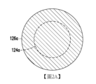
請參照圖1D,進行微影與蝕刻製程,以圖案化第一電極材料層122,形成與介層窗114電性連接的第一電極122a。第一電極122a為柱狀體,例如是圓柱體或是六面體(如圖3與圖4所示)。第一電極122a的頂面的上視圖可以是圓形、具有圓形導角的矩形等,分別如圖2A與圖2B所示。第一電極122a的頂面的上視圖也可以其他各種形狀,例如是橢圓形等。Referring to FIG. 1D , lithography and etching processes are performed to pattern the first
請參照圖1E,在第一電極122a的頂面與側壁以及阻擋材料層120上形成可變電阻材料層124。在一些實施例中,可變電阻材料層124為共形層,共形地覆蓋第一電極122a的頂面與側壁以及阻擋材料層120。在一些實施例中,阻擋材料層120為平坦層,因此,可變電阻材料層124的底面與第一電極122a的底面共平面。可變電阻材料層124的材料包括金屬氧化物,例如氧化鉿(HfO
2)、氧化鉭(Ta
2O
5)、氧化鈦(TiO
2)、氧化鎂(MgO)、氧化鎳(NiO)、氧化鈮(Nb
2O
5)、氧化鋁(Al
2O
3)、氧化釩(V
2O
5)、氧化鎢(WO
3)、氧化鋅(ZnO)或氧化鈷(CoO)。
1E , a variable
請參照圖1F,在可變電阻材料層124上形成第二電極材料層126。第二電極材料層126例如是氮化鈦(TiN)、氮化鉭(TaN)、氮化鈦鋁(TiAlN)、鈦鎢(TiW)合金、鉑(Pt)、銥(Ir)、釕(Ru)、鈦(Ti)、鎢(W)、鉭(Ta)、鋁(Al)、鋯(Zr)、鉿(Hf)、鎳(Ni)、銅(Cu)、鈷(Co)、鐵(Fe)、釓(Gd)、鉬(Mo)、石墨或上述材料的組合。第二電極材料層126可以是單層或是雙層。在一些實施例中,第二電極材料層126為雙層,其中上層可以是氮化鈦或氮化鉭,下層可以是銥。第二電極材料層126的厚度H2可以大於、等於或是小於第一電極122a的厚度H1。第二電極材料層126可以具有平坦的表面(如圖1E所示),或是與可變電阻材料層124共形(未示出)。1F , a second
請參照圖1F,進行微影與蝕刻製程,以圖案化第二電極材料層126、可變電阻材料層124以及阻擋材料層120,以形成第二電極126a、可變電阻層124a以及阻擋墊120a。在一些實施例中,第二電極126a、可變電阻層124a以及阻擋墊120a具有切齊的側壁。1F, lithography and etching processes are performed to pattern the second
請參照圖1G,在第二電極126a、可變電阻層124a以及阻擋墊120a的側壁形成間隙壁128。間隙壁128包括含氮的介電材料層,例如是氮化矽。間隙壁128與阻擋墊120a可包括相同的材料。間隙壁128的形成方法例如是先形成間隙壁材料層,以覆蓋第二電極126a、可變電阻層124a以及阻擋墊120a的側壁以及介電層110的表面。然後,再進行非等向性蝕刻製程。Referring to FIG. 1G , a
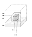
至此,形成了電阻式隨機存取記憶體150。電阻式隨機存取記憶體150具有間隙壁128與阻擋墊120a,其分別覆蓋可變電阻層124a的側壁與底面,且間隙壁128向上延伸覆蓋第二電極126的下側壁。在一些實施例中,間隙壁128覆蓋第二電極126的1/2~2/3的側壁。間隙壁128與阻擋墊120a可以共同阻擋水氣、金屬原子(例如銅原子)或氧等擴散至可變電阻層124a中。At this point, the
請參照圖1G與圖3,本發明實施例的電阻式隨機存取記憶體150的第一電極122a為柱狀體。可變電阻層124a夾於第一電極122a的頂面與第二電極126a之間以及第一電極122a的側壁與第二電極126a之間。而且,可變電阻層124a位於第二電極126a的底面與阻擋墊120a之間。可變電阻層124a可藉由阻擋墊120a與介電層110分離非零距離,以避免接觸介電層110,進而防止介電層110中的氧擴散至可變電阻層124a。1G and 3, the
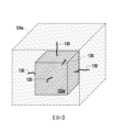
請參照圖1G與圖4,在進行設置(SET)操作時,對電阻式隨機存取記憶體150施加正電壓,可變電阻層124a中的氧離子在受正電壓吸引離開而產生氧空缺(oxygen vacancy),因而形成導電絲(filament)130並呈現導通狀態,此時可變電阻層由高電阻狀態(HRS)轉換到低電阻狀態(Low Resistance State,LRS)。當進行重置(RESET)操作時,對電阻式隨機存取記憶體150施加負偏壓,氧離子會回到可變電阻層124a中,使導電絲130斷裂並呈現非導通狀態,此時可變電阻層由LRS轉換到HRS。在本發明實施例中,由於第一電極122a呈柱狀體,且可變電阻層124a覆蓋柱狀體的頂面與側壁,因此,可以在第一電極122a的頂面與側壁上的可變電阻層124a中形成多個導電絲130。Please refer to FIG. 1G and FIG. 4 . When performing a set (SET) operation, a positive voltage is applied to the
本發明實施例之電阻式隨機存取記憶的結構可以在更多的區域形成導電絲,因此可以增加電阻式隨機存取記憶單元的低電阻狀態的電流量。The structure of the RRAM of the embodiment of the present invention can form conductive filaments in more areas, thereby increasing the current flow of the RRAM unit in the low resistance state.
100:基底
102:元件層
104、110:介電層
105:插塞
106:導線
107:金屬內連線
108:停止層
112:金屬內連線結構
113:介層窗孔
114:介層窗
120:阻擋材料層
120a:阻擋墊
122:第一電極材料層
122a:第一電極
124:可變電阻材料層
124a:可變電阻層
126:第二電極材料層
126a:第二電極
128:間隙壁
130:導電絲
150:電阻式隨機存取記憶體
H1、H2:厚度
100: substrate
102:
圖1A至圖1G是依照本發明的實施例的一種電阻式隨機存取記憶體的製造方法的剖面示意圖。 圖2A與圖2B是依照本發明的實施例的各種電阻式隨機存取記憶體的上視圖。 圖3是依照本發明的實施例的一種電阻式隨機存取記憶體單元的局部立體圖。 圖4是繪示圖3的局部放大圖。 Figures 1A to 1G are cross-sectional schematic diagrams of a method for manufacturing a resistive random access memory according to an embodiment of the present invention. Figures 2A and 2B are top views of various resistive random access memories according to an embodiment of the present invention. Figure 3 is a partial three-dimensional diagram of a resistive random access memory unit according to an embodiment of the present invention. Figure 4 is a partial enlarged diagram of Figure 3.
122a:第一電極 122a: first electrode
124a:可變電阻層 124a: variable resistance layer
130:導電絲 130: Conductive wire
Claims (16)
Priority Applications (3)
| Application Number | Priority Date | Filing Date | Title |
|---|---|---|---|
| TW110126483A TWI874686B (en) | 2021-07-19 | 2021-07-19 | Resistive random-access memorycell and method of fabricating the same |
| CN202110890937.0A CN115643787B (en) | 2021-07-19 | 2021-08-04 | Resistive random access memory device and its manufacturing method |
| US17/404,934 US11864473B2 (en) | 2021-07-19 | 2021-08-17 | Resistive random-access memory device and method of fabricating the same |
Applications Claiming Priority (1)
| Application Number | Priority Date | Filing Date | Title |
|---|---|---|---|
| TW110126483A TWI874686B (en) | 2021-07-19 | 2021-07-19 | Resistive random-access memorycell and method of fabricating the same |
Publications (2)
| Publication Number | Publication Date |
|---|---|
| TW202306108A TW202306108A (en) | 2023-02-01 |
| TWI874686B true TWI874686B (en) | 2025-03-01 |
Family
ID=84890879
Family Applications (1)
| Application Number | Title | Priority Date | Filing Date |
|---|---|---|---|
| TW110126483A TWI874686B (en) | 2021-07-19 | 2021-07-19 | Resistive random-access memorycell and method of fabricating the same |
Country Status (3)
| Country | Link |
|---|---|
| US (1) | US11864473B2 (en) |
| CN (1) | CN115643787B (en) |
| TW (1) | TWI874686B (en) |
Families Citing this family (1)
| Publication number | Priority date | Publication date | Assignee | Title |
|---|---|---|---|---|
| TWI761193B (en) * | 2021-04-28 | 2022-04-11 | 華邦電子股份有限公司 | Resistive random access memory cell and method of fabricating the same |
Citations (3)
| Publication number | Priority date | Publication date | Assignee | Title |
|---|---|---|---|---|
| US10014469B2 (en) * | 2013-09-09 | 2018-07-03 | Taiwan Semiconductor Manufacturing Company Ltd. | Resistive random access memory and manufacturing method thereof |
| TW201834289A (en) * | 2016-12-15 | 2018-09-16 | 南韓商三星電子股份有限公司 | Variable resistance memory device |
| TW201926751A (en) * | 2017-11-29 | 2019-07-01 | 台灣積體電路製造股份有限公司 | Memory cell and memory device |
Family Cites Families (22)
| Publication number | Priority date | Publication date | Assignee | Title |
|---|---|---|---|---|
| US7521705B2 (en) * | 2005-08-15 | 2009-04-21 | Micron Technology, Inc. | Reproducible resistance variable insulating memory devices having a shaped bottom electrode |
| KR20100133763A (en) * | 2009-06-12 | 2010-12-22 | 광주과학기술원 | Nonvolatile resistance change memory device and manufacturing method thereof |
| WO2011016196A1 (en) * | 2009-08-03 | 2011-02-10 | パナソニック株式会社 | Method for manufacturing semiconductor memory |
| JP2013168454A (en) * | 2012-02-14 | 2013-08-29 | Panasonic Corp | Semiconductor memory device and method for manufacturing the same |
| US9196828B2 (en) * | 2012-06-25 | 2015-11-24 | Macronix International Co., Ltd. | Resistive memory and fabricating method thereof |
| US9231205B2 (en) * | 2013-03-13 | 2016-01-05 | Taiwan Semiconductor Manufacturing Company, Ltd. | Low form voltage resistive random access memory (RRAM) |
| US9837605B2 (en) * | 2013-08-16 | 2017-12-05 | Taiwan Semiconductor Manufacturing Company, Ltd. | Memory cell having resistance variable film and method of making the same |
| CN104681716B (en) * | 2013-11-27 | 2018-03-13 | 华邦电子股份有限公司 | Resistive memory and manufacturing method thereof |
| US9257642B1 (en) * | 2014-07-16 | 2016-02-09 | Taiwan Semiconductor Manufacturing Co., Ltd. | Protective sidewall techniques for RRAM |
| TWI559452B (en) * | 2015-10-26 | 2016-11-21 | 國立中山大學 | Resistance random access memory |
| CN106654004B (en) * | 2015-10-29 | 2019-03-19 | 华邦电子股份有限公司 | Resistive memory and manufacturing method thereof |
| US9553265B1 (en) * | 2016-01-14 | 2017-01-24 | Taiwan Semiconductor Manufacturing Co., Ltd. | RRAM device with data storage layer having increased height |
| TWI713242B (en) * | 2017-01-23 | 2020-12-11 | 聯華電子股份有限公司 | Resistive random access memory and method of forming the same |
| US10680172B2 (en) * | 2017-11-13 | 2020-06-09 | Taiwan Semiconductor Manufacturing Co., Ltd. | Resistive random access memory device |
| US10559625B1 (en) * | 2018-08-08 | 2020-02-11 | International Business Machines Corporation | RRAM cells in crossbar array architecture |
| JP7052736B2 (en) * | 2019-01-08 | 2022-04-12 | 住友電装株式会社 | Inner conductor terminal and shield terminal |
| US11489118B2 (en) * | 2019-03-04 | 2022-11-01 | International Business Machines Corporation | Reliable resistive random access memory |
| US10847578B1 (en) * | 2019-07-03 | 2020-11-24 | Windbond Electronics Corp. | Three-dimensional resistive memories and methods for forming the same |
| TWI716235B (en) * | 2019-12-24 | 2021-01-11 | 華邦電子股份有限公司 | Resistive random access memory and manufacturing method thereof |
| US11424407B2 (en) * | 2020-09-02 | 2022-08-23 | Winbond Electronics Corp. | Resistive random access memory and method of manufacturing the same |
| TWI865720B (en) * | 2021-02-01 | 2024-12-11 | 聯華電子股份有限公司 | Rram device and forming method thereof |
| CN113611796A (en) * | 2021-04-16 | 2021-11-05 | 联芯集成电路制造(厦门)有限公司 | Resistive random access memory and manufacturing method thereof |
-
2021
- 2021-07-19 TW TW110126483A patent/TWI874686B/en active
- 2021-08-04 CN CN202110890937.0A patent/CN115643787B/en active Active
- 2021-08-17 US US17/404,934 patent/US11864473B2/en active Active
Patent Citations (3)
| Publication number | Priority date | Publication date | Assignee | Title |
|---|---|---|---|---|
| US10014469B2 (en) * | 2013-09-09 | 2018-07-03 | Taiwan Semiconductor Manufacturing Company Ltd. | Resistive random access memory and manufacturing method thereof |
| TW201834289A (en) * | 2016-12-15 | 2018-09-16 | 南韓商三星電子股份有限公司 | Variable resistance memory device |
| TW201926751A (en) * | 2017-11-29 | 2019-07-01 | 台灣積體電路製造股份有限公司 | Memory cell and memory device |
Also Published As
| Publication number | Publication date |
|---|---|
| US20230020564A1 (en) | 2023-01-19 |
| CN115643787A (en) | 2023-01-24 |
| TW202306108A (en) | 2023-02-01 |
| US11864473B2 (en) | 2024-01-02 |
| CN115643787B (en) | 2026-03-20 |
Similar Documents
| Publication | Publication Date | Title |
|---|---|---|
| CN109786549B (en) | Resistive random access memory device | |
| TWI744165B (en) | Resistive random access memory and method of fabricating the same | |
| TWI405331B (en) | Resistance switching memory | |
| US8871561B2 (en) | Variable resistance nonvolatile storage device and method for manufacturing the same | |
| TW202240854A (en) | Semiconductor memory devices | |
| WO2010050094A1 (en) | Nonvolatile semiconductor storage device and manufacturing method therefor | |
| CN114078901B (en) | Resistive storage devices and their manufacturing methods | |
| CN104377302B (en) | Memory cell and its manufacture method with resistance-variable film | |
| JP2017055082A (en) | Manufacturing method for nonvolatile storage device | |
| CN110021704B (en) | Resistive random access memory device | |
| TWI874686B (en) | Resistive random-access memorycell and method of fabricating the same | |
| EP2099071B1 (en) | Resistance change device and process for producing the same | |
| US20080090376A1 (en) | Method of fabricating semiconductor device | |
| TWI431825B (en) | Cross-point resistive memory array and method for manufacturing the same | |
| US12114579B2 (en) | Method of fabricating resistive random access memory cell | |
| JP2014082279A (en) | Nonvolatile storage device and manufacturing method thereof | |
| KR20140028421A (en) | Semiconductor device and method for fabricating the same | |
| US20140021432A1 (en) | Variable resistance memory device and method for fabricating the same | |
| TWI707455B (en) | Non-volatile memory and method of fabricating the same | |
| CN115117236B (en) | Resistive random access memory and manufacturing method thereof | |
| TWI747366B (en) | Resistive random access memory and method of fabricating the same | |
| JP7667810B2 (en) | Resistive memory device having ultra-thin barrier layer and method for forming same | |
| CN114005851B (en) | Resistive random access memory and manufacturing method thereof | |
| CN113838833B (en) | Semiconductor device and manufacturing method thereof | |
| CN119156020A (en) | Resistive memory device and method for manufacturing the same |