TWI866912B - Light emitting device - Google Patents
Light emitting device Download PDFInfo
- Publication number
- TWI866912B TWI866912B TW108120328A TW108120328A TWI866912B TW I866912 B TWI866912 B TW I866912B TW 108120328 A TW108120328 A TW 108120328A TW 108120328 A TW108120328 A TW 108120328A TW I866912 B TWI866912 B TW I866912B
- Authority
- TW
- Taiwan
- Prior art keywords
- light
- fluorescent
- peak wavelength
- range
- fluorescent body
- Prior art date
Links
Images


Classifications
-
- H—ELECTRICITY
- H10—SEMICONDUCTOR DEVICES; ELECTRIC SOLID-STATE DEVICES NOT OTHERWISE PROVIDED FOR
- H10H—INORGANIC LIGHT-EMITTING SEMICONDUCTOR DEVICES HAVING POTENTIAL BARRIERS
- H10H20/00—Individual inorganic light-emitting semiconductor devices having potential barriers, e.g. light-emitting diodes [LED]
- H10H20/80—Constructional details
- H10H20/85—Packages
- H10H20/851—Wavelength conversion means
- H10H20/8511—Wavelength conversion means characterised by their material, e.g. binder
- H10H20/8512—Wavelength conversion materials
-
- C—CHEMISTRY; METALLURGY
- C09—DYES; PAINTS; POLISHES; NATURAL RESINS; ADHESIVES; COMPOSITIONS NOT OTHERWISE PROVIDED FOR; APPLICATIONS OF MATERIALS NOT OTHERWISE PROVIDED FOR
- C09K—MATERIALS FOR MISCELLANEOUS APPLICATIONS, NOT PROVIDED FOR ELSEWHERE
- C09K11/00—Luminescent materials, e.g. electroluminescent or chemiluminescent
- C09K11/08—Luminescent materials, e.g. electroluminescent or chemiluminescent containing inorganic luminescent materials
- C09K11/58—Luminescent materials, e.g. electroluminescent or chemiluminescent containing inorganic luminescent materials containing copper, silver or gold
- C09K11/582—Chalcogenides
- C09K11/584—Chalcogenides with zinc or cadmium
-
- C—CHEMISTRY; METALLURGY
- C09—DYES; PAINTS; POLISHES; NATURAL RESINS; ADHESIVES; COMPOSITIONS NOT OTHERWISE PROVIDED FOR; APPLICATIONS OF MATERIALS NOT OTHERWISE PROVIDED FOR
- C09K—MATERIALS FOR MISCELLANEOUS APPLICATIONS, NOT PROVIDED FOR ELSEWHERE
- C09K11/00—Luminescent materials, e.g. electroluminescent or chemiluminescent
- C09K11/08—Luminescent materials, e.g. electroluminescent or chemiluminescent containing inorganic luminescent materials
- C09K11/77—Luminescent materials, e.g. electroluminescent or chemiluminescent containing inorganic luminescent materials containing rare earth metals
- C09K11/7728—Luminescent materials, e.g. electroluminescent or chemiluminescent containing inorganic luminescent materials containing rare earth metals containing europium
- C09K11/7734—Aluminates
-
- C—CHEMISTRY; METALLURGY
- C09—DYES; PAINTS; POLISHES; NATURAL RESINS; ADHESIVES; COMPOSITIONS NOT OTHERWISE PROVIDED FOR; APPLICATIONS OF MATERIALS NOT OTHERWISE PROVIDED FOR
- C09K—MATERIALS FOR MISCELLANEOUS APPLICATIONS, NOT PROVIDED FOR ELSEWHERE
- C09K11/00—Luminescent materials, e.g. electroluminescent or chemiluminescent
- C09K11/08—Luminescent materials, e.g. electroluminescent or chemiluminescent containing inorganic luminescent materials
- C09K11/77—Luminescent materials, e.g. electroluminescent or chemiluminescent containing inorganic luminescent materials containing rare earth metals
- C09K11/7783—Luminescent materials, e.g. electroluminescent or chemiluminescent containing inorganic luminescent materials containing rare earth metals containing two or more rare earth metals one of which being europium
- C09K11/7784—Chalcogenides
- C09K11/7787—Oxides
- C09K11/7789—Oxysulfides
-
- C—CHEMISTRY; METALLURGY
- C09—DYES; PAINTS; POLISHES; NATURAL RESINS; ADHESIVES; COMPOSITIONS NOT OTHERWISE PROVIDED FOR; APPLICATIONS OF MATERIALS NOT OTHERWISE PROVIDED FOR
- C09K—MATERIALS FOR MISCELLANEOUS APPLICATIONS, NOT PROVIDED FOR ELSEWHERE
- C09K11/00—Luminescent materials, e.g. electroluminescent or chemiluminescent
- C09K11/08—Luminescent materials, e.g. electroluminescent or chemiluminescent containing inorganic luminescent materials
- C09K11/77—Luminescent materials, e.g. electroluminescent or chemiluminescent containing inorganic luminescent materials containing rare earth metals
- C09K11/7783—Luminescent materials, e.g. electroluminescent or chemiluminescent containing inorganic luminescent materials containing rare earth metals containing two or more rare earth metals one of which being europium
- C09K11/77927—Silicon Nitrides or Silicon Oxynitrides
-
- H—ELECTRICITY
- H01—ELECTRIC ELEMENTS
- H01S—DEVICES USING THE PROCESS OF LIGHT AMPLIFICATION BY STIMULATED EMISSION OF RADIATION [LASER] TO AMPLIFY OR GENERATE LIGHT; DEVICES USING STIMULATED EMISSION OF ELECTROMAGNETIC RADIATION IN WAVE RANGES OTHER THAN OPTICAL
- H01S5/00—Semiconductor lasers
- H01S5/005—Optical components external to the laser cavity, specially adapted therefor, e.g. for homogenisation or merging of the beams or for manipulating laser pulses, e.g. pulse shaping
- H01S5/0087—Optical components external to the laser cavity, specially adapted therefor, e.g. for homogenisation or merging of the beams or for manipulating laser pulses, e.g. pulse shaping for illuminating phosphorescent or fluorescent materials, e.g. using optical arrangements specifically adapted for guiding or shaping laser beams illuminating these materials
-
- H—ELECTRICITY
- H05—ELECTRIC TECHNIQUES NOT OTHERWISE PROVIDED FOR
- H05B—ELECTRIC HEATING; ELECTRIC LIGHT SOURCES NOT OTHERWISE PROVIDED FOR; CIRCUIT ARRANGEMENTS FOR ELECTRIC LIGHT SOURCES, IN GENERAL
- H05B33/00—Electroluminescent light sources
- H05B33/12—Light sources with substantially two-dimensional [2D] radiating surfaces
- H05B33/14—Light sources with substantially two-dimensional [2D] radiating surfaces characterised by the chemical or physical composition or the arrangement of the electroluminescent material, or by the simultaneous addition of the electroluminescent material in or onto the light source
-
- H—ELECTRICITY
- H10—SEMICONDUCTOR DEVICES; ELECTRIC SOLID-STATE DEVICES NOT OTHERWISE PROVIDED FOR
- H10H—INORGANIC LIGHT-EMITTING SEMICONDUCTOR DEVICES HAVING POTENTIAL BARRIERS
- H10H20/00—Individual inorganic light-emitting semiconductor devices having potential barriers, e.g. light-emitting diodes [LED]
- H10H20/80—Constructional details
- H10H20/85—Packages
- H10H20/851—Wavelength conversion means
- H10H20/8511—Wavelength conversion means characterised by their material, e.g. binder
- H10H20/8512—Wavelength conversion materials
- H10H20/8513—Wavelength conversion materials having two or more wavelength conversion materials
-
- H—ELECTRICITY
- H10—SEMICONDUCTOR DEVICES; ELECTRIC SOLID-STATE DEVICES NOT OTHERWISE PROVIDED FOR
- H10H—INORGANIC LIGHT-EMITTING SEMICONDUCTOR DEVICES HAVING POTENTIAL BARRIERS
- H10H20/00—Individual inorganic light-emitting semiconductor devices having potential barriers, e.g. light-emitting diodes [LED]
- H10H20/80—Constructional details
- H10H20/85—Packages
- H10H20/851—Wavelength conversion means
- H10H20/8514—Wavelength conversion means characterised by their shape, e.g. plate or foil
-
- H—ELECTRICITY
- H10—SEMICONDUCTOR DEVICES; ELECTRIC SOLID-STATE DEVICES NOT OTHERWISE PROVIDED FOR
- H10K—ORGANIC ELECTRIC SOLID-STATE DEVICES
- H10K50/00—Organic light-emitting devices
-
- H—ELECTRICITY
- H10—SEMICONDUCTOR DEVICES; ELECTRIC SOLID-STATE DEVICES NOT OTHERWISE PROVIDED FOR
- H10K—ORGANIC ELECTRIC SOLID-STATE DEVICES
- H10K59/00—Integrated devices, or assemblies of multiple devices, comprising at least one organic light-emitting element covered by group H10K50/00
- H10K59/30—Devices specially adapted for multicolour light emission
- H10K59/38—Devices specially adapted for multicolour light emission comprising colour filters or colour changing media [CCM]
-
- H—ELECTRICITY
- H10—SEMICONDUCTOR DEVICES; ELECTRIC SOLID-STATE DEVICES NOT OTHERWISE PROVIDED FOR
- H10K—ORGANIC ELECTRIC SOLID-STATE DEVICES
- H10K85/00—Organic materials used in the body or electrodes of devices covered by this subclass
- H10K85/60—Organic compounds having low molecular weight
-
- H—ELECTRICITY
- H10—SEMICONDUCTOR DEVICES; ELECTRIC SOLID-STATE DEVICES NOT OTHERWISE PROVIDED FOR
- H10H—INORGANIC LIGHT-EMITTING SEMICONDUCTOR DEVICES HAVING POTENTIAL BARRIERS
- H10H20/00—Individual inorganic light-emitting semiconductor devices having potential barriers, e.g. light-emitting diodes [LED]
- H10H20/80—Constructional details
- H10H20/85—Packages
- H10H20/851—Wavelength conversion means
- H10H20/8515—Wavelength conversion means not being in contact with the bodies
-
- H—ELECTRICITY
- H10—SEMICONDUCTOR DEVICES; ELECTRIC SOLID-STATE DEVICES NOT OTHERWISE PROVIDED FOR
- H10K—ORGANIC ELECTRIC SOLID-STATE DEVICES
- H10K50/00—Organic light-emitting devices
- H10K50/10—OLEDs or polymer light-emitting diodes [PLED]
- H10K50/11—OLEDs or polymer light-emitting diodes [PLED] characterised by the electroluminescent [EL] layers
Landscapes
- Chemical & Material Sciences (AREA)
- Engineering & Computer Science (AREA)
- Materials Engineering (AREA)
- Physics & Mathematics (AREA)
- Inorganic Chemistry (AREA)
- Organic Chemistry (AREA)
- Optics & Photonics (AREA)
- General Physics & Mathematics (AREA)
- Electromagnetism (AREA)
- Condensed Matter Physics & Semiconductors (AREA)
- Spectroscopy & Molecular Physics (AREA)
- Led Device Packages (AREA)
- Luminescent Compositions (AREA)
- Electroluminescent Light Sources (AREA)
- Semiconductor Lasers (AREA)
Abstract
提供一種發光裝置,其藉由被來自光源的光激發而至 少在超過700nm的區域具有波峰波長。 A light emitting device is provided, which has a peak wavelength in a region exceeding 700 nm at least by being excited by light from a light source.
一種發光裝置,具備:發出在480nm以下的範圍 內具有波峰波長的光的固體光源、和覆蓋該固體光源且含有至少一種螢光體的螢光膜,螢光膜含有:至少一種近紅外螢光體,其被來自前述固體光源的光激發而在超過700nm的範圍內具有波峰波長,且包含該波峰波長的範圍內的發光光譜的半高全寬為100nm以上。 A light-emitting device comprises: a solid light source that emits light having a peak wavelength in a range below 480nm, and a fluorescent film that covers the solid light source and contains at least one fluorescent body, wherein the fluorescent film contains: at least one near-infrared fluorescent body that is excited by light from the solid light source and has a peak wavelength in a range exceeding 700nm, and the half-maximum full width of the luminescence spectrum in the range including the peak wavelength is greater than 100nm.
Description
本發明係關於發光裝置。 The present invention relates to a light emitting device.
近年來,以家庭用照明為首的各種照明,正迅速地從鹵素燈替換為發光二極體(LED),從而變得可以實現長壽命化及小型化。但是,分光分析裝置等的產業機器用的光源絕大多數仍使用鹵素燈,而沒有替換為LED。其較大的原因,認為是以往的LED很難滿足產業機器用的光源所要求的下述特性:呈現出寬廣頻帶下穩定的發光光譜分布、不易發生溫度變化所造成的波長偏移等。專利文獻1中記載:含有包含紅色螢光體和綠色螢光體的2種以上螢光體的發光裝置用的多層膜片,其中各個螢光體層中所含的螢光體係一個種類,且依照從含有長發光波長螢光體的螢光體層到含有短發光波長螢光體的螢光體層的順序進行配置,藉此來提高發光裝置的全光束。 In recent years, various lighting, including household lighting, has been rapidly replaced from halogen lamps to light-emitting diodes (LEDs), which have become longer-lasting and smaller. However, the vast majority of light sources for industrial equipment such as spectroscopic analysis devices still use halogen lamps instead of LEDs. The main reason for this is that it is believed that LEDs in the past have difficulty meeting the following characteristics required of light sources for industrial equipment: stable luminous spectrum distribution over a wide bandwidth, and wavelength shifts that are not easily caused by temperature changes.
專利文獻1:日本特開2015-130459號公報 Patent document 1: Japanese Patent Application Publication No. 2015-130459
然而,以往的發光裝置係以適用於照明用途為目的的發光裝置,因此是高波長側的波峰波長於700nm以下者,不 足以作為被要求在超過700nm的近紅外線區域亦具有波峰波長的發光的產業機器用光源。 However, conventional light-emitting devices are light-emitting devices intended for lighting purposes, and therefore have a peak wavelength on the high-wavelength side of less than 700nm, which is insufficient as a light source for industrial equipment that is required to have a peak wavelength in the near-infrared region exceeding 700nm.
本發明的課題在於提供一種發光裝置,其藉由被來自光源的光激發而至少在超過700nm的區域具有波峰波長。 The present invention provides a light emitting device which has a peak wavelength in a region exceeding 700 nm by being excited by light from a light source.
本發明係關於以下內容的發明。 The present invention relates to the following aspects.
一種發光裝置,至少具備:發出在480nm以下的範圍內具有波峰波長的光的固體光源、和覆蓋該固體光源且含有至少一種螢光體的螢光膜,前述螢光膜含有:至少一種近紅外螢光體,其被來自前述固體光源的光激發而發出在超過700nm的範圍內具有波峰波長,且包含該波峰波長的範圍內的發光光譜的半高全寬為100nm以上的光。 A light-emitting device comprises at least: a solid light source emitting light having a peak wavelength in a range below 480 nm, and a fluorescent film covering the solid light source and containing at least one kind of fluorescent body, wherein the fluorescent film contains: at least one kind of near-infrared fluorescent body which is excited by the light from the solid light source to emit light having a peak wavelength in a range exceeding 700 nm, and the half-maximum full width of the luminescence spectrum in the range including the peak wavelength is greater than 100 nm.
如[1]的發光裝置,其至少在400nm以上1000nm以下的範圍內具有連續發光光譜。 The light-emitting device of [1] has a continuous light-emitting spectrum at least in the range of 400 nm to 1000 nm.
如[1]或[2]的發光裝置,其中前述螢光膜進一步含有:至少一種可見光螢光體,其被來自前述固體光源的光激發而發出在350nm以上700nm以下的範圍內具有波峰波長的光。 The light-emitting device of [1] or [2], wherein the fluorescent film further comprises: at least one visible light fluorescent body, which is excited by the light from the solid light source to emit light having a peak wavelength in the range of 350 nm to 700 nm.
如[3]的發光裝置,其中前述螢光膜分別包含一種以上的可見光螢光體A、可見光螢光體B、可見光螢光體C作為前述可見光螢光體,該可見光螢光體A被來自前述固體光源的光激發而發出在350nm以上小於430nm的範圍內具有波峰波長的光,該可見光螢光體B被來自前述固體光源的光激發而發出在430nm以上小於500nm的範圍內具有波峰波長的光,該可見光螢光體C被來自前述固體光源的光激發而發出在500nm以上700nm以下的範圍內具有波峰波長的光。 A light-emitting device as described in [3], wherein the fluorescent film comprises one or more visible light fluorescent bodies A, visible light fluorescent body B, and visible light fluorescent body C as the visible light fluorescent bodies, the visible light fluorescent body A is excited by the light from the solid light source to emit light having a peak wavelength in the range of 350 nm to less than 430 nm, the visible light fluorescent body B is excited by the light from the solid light source to emit light having a peak wavelength in the range of 430 nm to less than 500 nm, and the visible light fluorescent body C is excited by the light from the solid light source to emit light having a peak wavelength in the range of 500 nm to less than 700 nm.
如[4]的發光裝置,其中前述螢光膜係以2個以上的層形成,前述可見光螢光體A及B係包含在不同的層中。 In the light-emitting device of [4], the fluorescent film is formed of two or more layers, and the visible light fluorescent bodies A and B are contained in different layers.
如[4]或[5]的發光裝置,其中前述螢光膜係以所含的前述螢光體的種類不同的2個以上的層形成,該2個以上的層係依照從含有波峰波長較長的螢光體的層到含有波峰波長較短的螢光體的層的順序,在來自前述固體光源的光的行進方向上積層。 A light-emitting device as in [4] or [5], wherein the fluorescent film is formed of two or more layers containing the fluorescent bodies of different types, and the two or more layers are stacked in the direction of travel of light from the solid light source in the order from a layer containing a fluorescent body with a longer peak wavelength to a layer containing a fluorescent body with a shorter peak wavelength.
如[5]或[6]的發光裝置,其中前述螢光膜各層中所含的前述螢光體的種類為1以上3以下。 In the light-emitting device of [5] or [6], the number of types of the fluorescent bodies contained in each layer of the fluorescent film is greater than 1 and less than 3.
如[4]的發光裝置,其中前述螢光膜係在同一面上具有所含的前述螢光體的種類不同的2個以上的區域。 In the light-emitting device of [4], the fluorescent film has two or more regions containing different types of fluorescent bodies on the same surface.
如[8]的發光裝置,其中前述螢光體的種類不同的2個以上的區域至少具有:含有前述近紅外螢光體的區域、及含有前述可見光螢光體的區域。 In the light-emitting device of [8], the two or more regions of different types of fluorescent bodies include at least: a region containing the near-infrared fluorescent body and a region containing the visible light fluorescent body.
如[1]至[9]中任一項的發光裝置,其具備2個以上的前述固體光源。 A light-emitting device as described in any one of [1] to [9], which has two or more of the aforementioned solid light sources.
如[1]至[10]中任一項的發光裝置,其中前述固體光源係從發光二極體、雷射二極體、及有機電致發光元件所選出的至少一種。 In the light-emitting device of any one of [1] to [10], the solid-state light source is at least one selected from a light-emitting diode, a laser diode, and an organic electroluminescent element.
如[1]至[11]中任一項的發光裝置,其中前述近紅外螢光體含有2價的銪離子。 A light-emitting device as described in any one of [1] to [11], wherein the near-infrared phosphor contains divalent iridium ions.
如[1]至[12]中任一項的發光裝置,其中前述近紅外螢光體具有以下述式(I)所示的組成,LiaSrbLacSidNeEuf...(I) The light-emitting device of any one of [1] to [12], wherein the near-infrared fluorescent body has a composition represented by the following formula (I): Li a S r b La c Si d Ne Eu f . . . (I)
(其中,a~f係滿足a+b+c+d+e+f=100、0≦a≦8.22、0.22≦b≦17.33、1.12≦c≦11.36、22.41≦d≦38.09、49.47≦e≦ 56.09、0.88≦f≦1.01的數字)。 (Among them, a~f are numbers that satisfy a+b+c+d+e+f=100, 0≦a≦8.22, 0.22≦b≦17.33, 1.12≦c≦11.36, 22.41≦d≦38.09, 49.47≦e≦56.09, 0.88≦f≦1.01).
一種螢光膜,含有:至少一種近紅外螢光體,其係藉由在480nm以下的範圍內具有波峰波長的光,來發出在超過700nm的範圍內具有波峰波長且包含該波峰波長的範圍內的發光光譜的半高全寬為100nm以上的光;和至少一種可見光螢光體,其係藉由前述光,來發出在350nm以上700nm以下的範圍內具有波峰波長的光。 A fluorescent film comprises: at least one near-infrared fluorescent body, which emits light having a peak wavelength in a range exceeding 700nm by using light having a peak wavelength in a range below 480nm, and the half-maximum full width of the luminescence spectrum in the range including the peak wavelength is 100nm or more; and at least one visible light fluorescent body, which emits light having a peak wavelength in a range above 350nm and below 700nm by using the above-mentioned light.
若根據本發明,便能夠提供一種發光裝置,其藉由被來自光源的光激發而至少在超過700nm的區域具有波峰波長。 According to the present invention, a light-emitting device can be provided, which has a peak wavelength in a region at least exceeding 700 nm by being excited by light from a light source.
1、11、12、13‧‧‧封裝體 1, 11, 12, 13...Package
2、21、22a~22e、23a~23f‧‧‧固體光源 2, 21, 22a~22e, 23a~23f‧‧‧Solid-state light sources
3、30、31、32a~32e、33a~33g‧‧‧螢光膜 3, 30, 31, 32a~32e, 33a~33g‧‧‧Fluorescent film
4‧‧‧導線 4. Conductor
5‧‧‧電極墊 5. Electrode pad
6‧‧‧靜電保護元件 6. Electrostatic protection components
10、100、101、102‧‧‧發光裝置 10, 100, 101, 102... Light-emitting devices
圖1係顯示一實施形態的發光裝置的構成的概略圖,(A)係平面圖,(B)係側面圖。 FIG. 1 is a schematic diagram showing the structure of a light-emitting device according to an embodiment, wherein (A) is a plan view and (B) is a side view.
圖2係顯示固體光源及螢光膜的積層例的說明圖。 FIG. 2 is an explanatory diagram showing an example of the stacking of a solid-state light source and a fluorescent film.
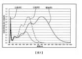
圖3係實施例中使用的近紅外螢光體P1~P7的發光光譜。A中顯示近紅外螢光體P1、P2的發光光譜。B中顯示近紅外螢光體P3、P4的發光光譜。C中顯示近紅外螢光體P5~P7的發光光譜。 FIG3 shows the luminescence spectra of near-infrared fluorescent bodies P1 to P7 used in the embodiment. A shows the luminescence spectra of near-infrared fluorescent bodies P1 and P2. B shows the luminescence spectra of near-infrared fluorescent bodies P3 and P4. C shows the luminescence spectra of near-infrared fluorescent bodies P5 to P7.
圖4係實施例中使用的近紅外螢光體P8~P14的發光光譜。D中顯示近紅外螢光體P8、P9的發光光譜。E中顯示近紅外螢光體P10、P11的發光光譜。F中顯示近紅外螢光體P12~14的發光光譜。 FIG. 4 shows the luminescence spectra of near-infrared phosphors P8 to P14 used in the embodiment. D shows the luminescence spectra of near-infrared phosphors P8 and P9. E shows the luminescence spectra of near-infrared phosphors P10 and P11. F shows the luminescence spectra of near-infrared phosphors P12 to P14.
圖5係實施例中使用的近紅外螢光體P8的發光光譜。 FIG. 5 is a luminescence spectrum of the near-infrared phosphor P8 used in the embodiment.
圖6係實施例1、3的發光裝置的發光光譜。 FIG6 is a luminescent spectrum of the luminescent device of
圖7係實施例2的發光裝置的發光光譜。 FIG7 is a luminescent spectrum of the luminescent device of Example 2.
圖8係實施例1及比較例1、2的發光裝置的發光光譜。 FIG8 is a luminescent spectrum of the luminescent devices of Example 1 and Comparative Examples 1 and 2.
圖9係顯示第1變形例的發光裝置的構成例的概略平面圖。 FIG9 is a schematic plan view showing a configuration example of a light emitting device according to a first modification.
圖10係顯示第1變形例的發光裝置的構成例的概略側面圖。 FIG10 is a schematic side view showing a configuration example of a light emitting device according to a first variation.
圖11係顯示第2變形例的發光裝置的構成例的概略平面圖。 FIG11 is a schematic plan view showing a configuration example of a light emitting device according to a second modification.
圖12係顯示第2變形例的發光裝置的構成例的概略平面圖。 FIG12 is a schematic plan view showing a configuration example of a light emitting device according to a second variation.
以下針對本發明的一實施形態詳細地進行說明。本發明不限於以下的實施形態,能夠在不妨礙本發明的效果的範圍內施加適宜變更來實施。 The following is a detailed description of one embodiment of the present invention. The present invention is not limited to the following embodiment, and can be implemented with appropriate modifications within the scope that does not hinder the effects of the present invention.
圖1中顯示:顯示一實施形態的發光裝置的構成的概略平面圖及側面圖。圖2中顯示:固體光源及螢光膜的積層例。圖1、2所示的發光裝置10具備:載置於封裝體1的固體光源2、和覆蓋該固體光源2的螢光膜3。封裝體1係以具有凹部的杯狀基體構成,在凹部的底面設有固體光源2,同時凹部的開口部分被螢光膜3覆蓋。又,圖1(A)中省略了螢光膜3。作為構成封裝體1的基體,能夠使用:使用了樹脂板、陶瓷板等的表面安裝用封裝體(SMD封裝體)或晶片板用基板(COB基板)等。固體光源2係使用未圖示的銀膏等的晶粒接著材來接合於封裝體1,同時以固體光源2的正極及負極與封裝體1的正極及負極各自的電極墊5 相連的方式,藉由包含金等的導線4來與封裝體1電性連接。又,在覆晶安裝的情況下,可以使用:使用了導電構件的突起狀端子來取代導線4以進行電性連接。在固體光源2的上側,自固體光源2的上表面隔開既定的空間,而設置螢光膜3,以覆蓋封裝體1的凹部的開口部且與固體光源2的上表面成為平行。藉此,螢光膜3係設置成覆蓋固體光源2整體且主面與來自固體光源2的光垂直地相交。 FIG1 shows: a schematic plan view and a side view showing the structure of a light-emitting device in an embodiment. FIG2 shows: an example of the lamination of a solid light source and a fluorescent film. The light-
圖2中,螢光膜3係以三層構成,但也可以是單層,也可以是二層以上的任意層數。層構成的細節如後述。在螢光膜3係以複數個層(2個以上的層)形成的情況下,各層係在來自固體光源2的光的行進方向上積層。圖1中,螢光膜3係設置成與固體光源的上表面隔著既定的空間,該空間可以藉由非活性氣體、樹脂、玻璃等透明構件等予以填充。此外,能夠以與固體光源2相接的方式設置螢光膜3。 In FIG. 2 , the
可以根據需要,如圖1所示,與固體光源2並列地將齊納二極體、ESD元件等的靜電保護元件6以導線4連接於電極墊5。 As required, as shown in FIG. 1 , an
固體光源係發出在480nm以下的範圍內具有波峰波長的光的固體光源。固體光源也能夠設為發出在450nm以下或410nm以下的範圍內具有波峰波長的光的固體光源。固體光源發出的光的波峰波長的範圍的下限值沒有特別的限定,能夠設為260nm以上、330nm以上、或350nm以上。又,在本說明書中,只要沒有特別的指定,「波峰波長」此用語係指分光發光光譜顯示出波峰的波長,將其中最大強度的波長稱為「最大波峰波長」。藉 由使用發出在上述範圍內具有波峰波長的光的固體光源,能夠使後述的各種螢光體被激發。此外,固體光源的發光光譜通常可以認為是半高全寬為10nm以上,且該發光光譜是採用按照高斯函數的強度分布,故截止波長(例如低於螢光強度在最大波峰波長時的強度的1.5%的波長)的寬度(短波長側截止波長和長波長側截止波長的間隔)為20nm以上,因此例如使用發出在400nm以下的範圍內具有波峰波長的光的固體光源,從而能夠作成具有380nm以下的紫外線區域的發光光譜的發光裝置。 A solid light source is a solid light source that emits light having a peak wavelength in a range below 480 nm. The solid light source can also be a solid light source that emits light having a peak wavelength in a range below 450 nm or below 410 nm. The lower limit of the range of the peak wavelength of light emitted by the solid light source is not particularly limited, and can be set to be above 260 nm, above 330 nm, or above 350 nm. In addition, in this specification, unless otherwise specified, the term "peak wavelength" refers to the wavelength at which the spectroscopic emission spectrum shows a peak, and the wavelength with the maximum intensity therein is referred to as the "maximum peak wavelength." By using a solid light source that emits light having a peak wavelength in the above range, various phosphors described later can be excited. Furthermore, the luminescence spectrum of a solid-state light source can generally be considered to have a full width at half maximum of more than 10 nm, and the luminescence spectrum adopts an intensity distribution according to a Gaussian function, so the width (interval between the cutoff wavelength on the short-wavelength side and the cutoff wavelength on the long-wavelength side) of the cutoff wavelength (for example, a wavelength lower than 1.5% of the intensity of the fluorescent intensity at the maximum peak wavelength) is more than 20 nm. Therefore, for example, by using a solid-state light source that emits light with a peak wavelength in the range below 400 nm, a light-emitting device having a luminescence spectrum in the ultraviolet region below 380 nm can be made.
作為固體光源,例如能使用從發光二極體(LED)、雷射二極體(LD)、及有機電致發光元件(有機EL元件)所選出的至少一種。作為LED或LD,例如能舉出InGaN系、GaN系、AlGaN系等的發出紫外線至紫色光的LED或LD。作為有機EL元件,例如能舉出發光層中包含從下述骨架中具有芳香族基的化合物所選出的一個以上的藍色系發光材料的有機EL元件等:萘、二苯乙烯基伸芳基(distyrylarylene)、噁唑、異噁唑、噁二唑、咪唑、咔唑、吡唑、吡咯、呋喃、呋呫(furazane)、苯并呋喃、異苯并呋喃、茀、吡啶、吡喃、苯并吡喃、吡


螢光膜係以覆蓋固體光源的方式設置,含有至少一種螢光體。螢光膜可以以單層構成,也可以以2個以上的層構成。螢光膜含有:至少一種近紅外螢光體(以下也簡稱為「近紅外螢光體」),其被來自固體光源的光激發而發出在超過700nm的範圍 (較佳為750nm以上的範圍)內具有波峰波長(較佳為最大波峰波長),且該發光光譜的半高全寬(full width at half maximun,FWHM)為100nm以上(較佳為120nm以上,更佳為150nm以上,特佳為200nm以上)的光。 The fluorescent film is provided in a manner covering the solid light source, and contains at least one kind of fluorescent body. The fluorescent film can be composed of a single layer or two or more layers. The fluorescent film contains: at least one kind of near-infrared fluorescent body (hereinafter also referred to as "near-infrared fluorescent body"), which is excited by the light from the solid light source and emits light having a peak wavelength (preferably a maximum peak wavelength) in a range exceeding 700nm (preferably a range exceeding 750nm), and the full width at half maximum (FWHM) of the emission spectrum is greater than 100nm (preferably greater than 120nm, more preferably greater than 150nm, and particularly preferably greater than 200nm).
又,在本說明書中,「近紅外螢光體」此用語係如上所述,意指「被來自固體光源的光激發而發出在超過700nm的範圍內具有波峰波長(較佳為最大波峰波長),且包含該波峰波長的範圍內的發光光譜的半高全寬為100nm以上的光的螢光體」。一般而言,「近紅外」此用語被用作指780nm~3000nm左右的波長範圍的用語。本實施形態中使用的近紅外螢光體,可以認為係在超過700nm的範圍內具有波峰波長且包含該波峰波長的範圍內的發光光譜的半高全寬為100nm以上,且該發光光譜是採用按照高斯函數的強度分布,故截止波長(例如低於螢光強度在最大波峰波長時的強度的1.5%的波長)的寬度(短波長側截止波長和長波長側截止波長的間隔)為200nm以上,因此至少在超過780nm的波長範圍內能夠呈現出光譜,從一般的含義來看也並不矛盾。 In addition, in this specification, the term "near-infrared fluorescent body" means "a fluorescent body which is excited by light from a solid light source and emits light having a peak wavelength (preferably a maximum peak wavelength) in a range exceeding 700nm, and a full width at half maximum of 100nm or more of the emission spectrum in the range of the peak wavelength" as described above. Generally speaking, the term "near-infrared" is used to refer to the wavelength range of about 780nm to 3000nm. The near-infrared phosphor used in the present embodiment can be considered to have a peak wavelength in the range exceeding 700nm and the half-maximum full width of the luminescence spectrum in the range including the peak wavelength is greater than 100nm, and the luminescence spectrum adopts an intensity distribution according to a Gaussian function, so the width (interval between the cutoff wavelength on the short-wavelength side and the cutoff wavelength on the long-wavelength side) of the cutoff wavelength (for example, a wavelength lower than 1.5% of the intensity of the fluorescent intensity at the maximum peak wavelength) is greater than 200nm, so that the spectrum can be presented at least in the wavelength range exceeding 780nm, which is not contradictory in the general sense.
因為含有「被來自固體光源的光激發而形成在超過700nm的範圍內具有波峰波長,且該發光光譜的半高全寬為50nm以上(特別是100nm以上)的寬廣波峰的近紅外螢光體」,因此能夠作成:藉由上述的由來自光源的光激發而在近紅外線區域具有一定強度並且寬廣的波峰波長的發光裝置。除此之外,與上述固體光源、後述的可根據需要而含有的可見光螢光體組合,能夠作成:具有從紫外線區域到近紅外線區域的寬廣頻帶的發光光譜的發光裝置。又,近紅外螢光體,在超過700nm的範圍內 (較佳為在750nm以上的範圍內)具有波峰波長即可,可以在其他的範圍內具有波峰波長。例如,近紅外螢光體也能夠以在600nm以上700nm以下的範圍內和在超過700nm的範圍內具有波峰波長的方式而構成。 Since it contains "a near-infrared phosphor that is excited by light from a solid light source and has a peak wavelength in a range exceeding 700nm, and the half-height full width of the luminescence spectrum is 50nm or more (especially 100nm or more)", it is possible to produce a light-emitting device that has a certain intensity and a wide peak wavelength in the near-infrared region by the light excitation from the light source. In addition, by combining the above-mentioned solid light source and the visible light phosphor that can be included as needed, it is possible to produce a light-emitting device having a wide-band luminescence spectrum from the ultraviolet region to the near-infrared region. Furthermore, the near-infrared fluorescent body only needs to have a peak wavelength in a range exceeding 700 nm (preferably in a range exceeding 750 nm), and may have a peak wavelength in other ranges. For example, the near-infrared fluorescent body may also be configured to have a peak wavelength in a range exceeding 600 nm and below 700 nm, and in a range exceeding 700 nm.
根據圖5,說明近紅外螢光體的發光光譜的一例。圖5係在後述的實施例使用的近紅外螢光體P8的發光光譜(光源:在370nm分光的氙燈)。如圖5所示,此近紅外螢光體在680±3nm、及776±3nm具有波峰波長。即,此近紅外螢光體在超過700nm的範圍內具有一個波峰波長。各發光光譜的半高全寬分別是113nm、及209nm。這兩者的波峰重疊,且包含兩者的發光光譜的截止波長(例如低於螢光強度在800nm時的強度的1.5%的波長)係短波長側為540±3nm,長波長側為1200±3nm。又,近紅外螢光體的發光光譜,在超過700nm的範圍內具有波峰波長即可,不限於與圖5所示的發光光譜相同的波形。 An example of the luminescence spectrum of a near-infrared fluorescent body is described with reference to FIG5. FIG5 is the luminescence spectrum of the near-infrared fluorescent body P8 used in the embodiment described later (light source: xenon lamp with spectral distribution at 370nm). As shown in FIG5, this near-infrared fluorescent body has peak wavelengths at 680±3nm and 776±3nm. That is, this near-infrared fluorescent body has a peak wavelength in the range of more than 700nm. The full width at half maximum of each luminescence spectrum is 113nm and 209nm respectively. The peaks of the two overlap, and the cutoff wavelength of the luminescence spectrum including both (for example, the wavelength lower than 1.5% of the intensity of the fluorescence intensity at 800nm) is 540±3nm on the short wavelength side and 1200±3nm on the long wavelength side. In addition, the luminescence spectrum of the near-infrared fluorescent body only needs to have a peak wavelength in the range of more than 700nm, and is not limited to the same waveform as the luminescence spectrum shown in Figure 5.
以使用了此近紅外螢光體的螢光膜(不含後述的可見光螢光體的螢光膜)、和上述固體光源所構成的發光裝置,強度平衡(balance)是任意的,但在與圖5大致相同的波長,具有波峰波長。 The light-emitting device composed of a fluorescent film using this near-infrared fluorescent body (excluding a fluorescent film using a visible light fluorescent body described later) and the above-mentioned solid light source has an arbitrary intensity balance, but has a peak wavelength at approximately the same wavelength as that in FIG. 5 .
作為近紅外螢光體,若為在上述範圍內具有波峰波長的螢光體,便沒有特別的限定,例如能舉出:銪或鈰活化氮化物或氮氧化物螢光體。它們係5d和4f之間的躍遷所產生的發光,半高寬為寬,因而較佳。特別是添加了2價的銪(2價的銪離子)的螢光體,其半高寬為寬且發光強度為高,因而更佳。 As a near-infrared phosphor, there is no particular limitation as long as it has a peak wavelength within the above range, and examples thereof include: indium or titanium activated nitride or nitrogen oxide phosphors. These are preferred because they emit light by a transition between 5d and 4f and have a wide half-height width. In particular, phosphors to which divalent indium (divalent indium ions) are added have a wide half-height width and high luminescence intensity, and are more preferred.
作為銪或鈰活化氮化物或氮氧化物螢光體,例如能舉出:以從包含Li、Sr、La、及Si的群組所選出的1個以上的 金屬的氮化物作為母體結晶,且該母體結晶中含有作為活化劑的銪的氮化物螢光體。 Examples of the idium- or titanium-activated nitride or oxynitride phosphor include a nitride phosphor having a matrix crystal made of a nitride of one or more metals selected from the group consisting of Li, Sr, La, and Si, and containing idium as an activator in the matrix crystal.
近紅外螢光體,設為具有以下述式(I)所示的組成的近紅外螢光體時,半高寬為寬,因而較佳,設為在下述式(I)中具有0.88≦f≦1.01的組成的近紅外螢光體時,發光強度為高,因而更佳。 When the near-infrared phosphor is a near-infrared phosphor having a composition represented by the following formula (I), the half-height width is wide, which is preferred. When the near-infrared phosphor is a near-infrared phosphor having a composition of 0.88≦f≦1.01 in the following formula (I), the luminous intensity is high, which is further preferred.
LiaSrbLacSidNeEuf...(I) Li a Sr b La c Si d N e Eu f . . . (I)
(其中,a~f係成為a+b+c+d+e+f=100、0≦a≦8.22、0.22≦b≦17.33、1.12≦c≦11.36、22.41≦d≦38.09、49.47≦e≦56.09、0.05≦f≦10的數字)。 (Among them, a~f are numbers such as a+b+c+d+e+f=100, 0≦a≦8.22, 0.22≦b≦17.33, 1.12≦c≦11.36, 22.41≦d≦38.09, 49.47≦e≦56.09, 0.05≦f≦10).
近紅外螢光體的含量,較佳為螢光膜中所含的全部螢光體中的5質量%以上50質量%以下,更佳為10質量%以上30質量%以下,再佳為15質量%以上25質量%以下。藉由設在上述範圍內,能夠不會妨礙其他螢光體層的發光地得到近紅外螢光體的發光。 The content of the near-infrared phosphor is preferably 5% by mass to 50% by mass of all the phosphors contained in the fluorescent film, more preferably 10% by mass to 30% by mass, and even more preferably 15% by mass to 25% by mass. By setting it within the above range, the luminescence of the near-infrared phosphor can be obtained without hindering the luminescence of other phosphor layers.
螢光膜,除了上述近紅外螢光體外,還可以含有:至少一種可見光螢光體(以下也簡稱為「可見光螢光體」),其被來自固體光源的光激發而發出在350nm以上700nm以下的範圍內具有波峰波長(較佳為最大波峰波長)的光。藉由含有可見光螢光體,能夠作成:具有達到紫外線區域、可見光區域及紅外線區域的寬廣頻帶的發光光譜的發光裝置。 The fluorescent film may contain, in addition to the above-mentioned near-infrared fluorescent body, at least one visible light fluorescent body (hereinafter also referred to as "visible light fluorescent body"), which is excited by light from a solid light source and emits light having a peak wavelength (preferably a maximum peak wavelength) in the range of 350 nm to 700 nm. By containing a visible light fluorescent body, a light-emitting device having a wide-band light emission spectrum reaching the ultraviolet region, the visible light region, and the infrared region can be produced.
又,在本說明書中,「可見光螢光體」此用語係如上所述,意指「被來自固體光源的光激發而發出在350nm以上700nm以下的範圍內具有波峰波長(較佳為最大波峰波長)的光的螢光體」。一般而言,「可見光」此用語被用作指380nm~780nm左 右的波長範圍的用語。本實施形態中使用的可見光螢光體,係在350nm以上700nm以下的範圍內具有波峰波長,且通常可以認為該發光光譜的半高全寬為50nm以上,且該發光光譜是採用按照高斯函數的強度分布,因此截止波長(例如低於螢光強度在最大波峰波長時的強度的1.5%的波長)的寬度(短波長側截止波長和長波長側截止波長的範圍)為100nm以上,因此可以涵蓋至少380nm~780nm左右的波長範圍全部區域地呈現出光譜,因此從一般的含義來看也並不矛盾。 In addition, in this specification, the term "visible light fluorescent body" means "a fluorescent body that is excited by light from a solid light source and emits light having a peak wavelength (preferably a maximum peak wavelength) in the range of 350nm to 700nm" as described above. Generally speaking, the term "visible light" is used as a term to refer to the wavelength range of about 380nm to 780nm. The visible light phosphor used in the present embodiment has a peak wavelength in the range of 350 nm to 700 nm, and the half-height full width of the luminescence spectrum can generally be considered to be 50 nm or more. The luminescence spectrum adopts an intensity distribution according to a Gaussian function, so the width of the cut-off wavelength (for example, a wavelength lower than 1.5% of the intensity of the fluorescence intensity at the maximum peak wavelength) (the range of the cut-off wavelength on the short wavelength side and the cut-off wavelength on the long wavelength side) is 100 nm or more, so the spectrum can be presented in the entire wavelength range of at least 380 nm to 780 nm, so there is no contradiction in the general sense.
作為可見光螢光體,若為在上述範圍內具有波峰波長的螢光體,便沒有特別的限定,例如能舉出:被來自固體光源的光激發而發出在350nm以上小於430nm的範圍內具有波峰波長的光的螢光體A(以下也簡稱為「可見光螢光體A」)、被來自固體光源的光激發而發出在430nm以上小於500nm的範圍內具有波峰波長的光的螢光體B(以下也簡稱為「可見光螢光體B」)、被來自固體光源的光激發而發出在500nm以上小於700nm的範圍內具有波峰波長的光的螢光體C(以下也簡稱為「可見光螢光體C」)。螢光體A~C較佳為分別在上述範圍內具有最大波峰波長。在更確實地呈現出寬廣頻帶的發光光譜的方面上,可見光螢光體較佳為各包含一種以上的螢光體A~C。又,可見光螢光體的波峰波長,能夠藉由調整可見光螢光體的活化劑的含量、調整混合物的混合比來調整為各區域內的任意的波長。 As a visible light fluorescent body, there is no particular limitation as long as it is a fluorescent body having a peak wavelength within the above-mentioned range. For example, there can be cited: fluorescent body A (hereinafter also referred to as "visible light fluorescent body A") which is excited by light from a solid light source and emits light with a peak wavelength in the range of 350nm to less than 430nm, fluorescent body B (hereinafter also referred to as "visible light fluorescent body B") which is excited by light from a solid light source and emits light with a peak wavelength in the range of 430nm to less than 500nm, and fluorescent body C (hereinafter also referred to as "visible light fluorescent body C") which is excited by light from a solid light source and emits light with a peak wavelength in the range of 500nm to less than 700nm. The fluorescent materials A to C preferably have maximum peak wavelengths within the above ranges, respectively. In order to more accurately present a wideband luminescence spectrum, the visible light fluorescent material preferably includes one or more fluorescent materials A to C. In addition, the peak wavelength of the visible light fluorescent material can be adjusted to any wavelength within each range by adjusting the content of the activator of the visible light fluorescent material and adjusting the mixing ratio of the mixture.
作為可見光螢光體A,例如能舉出:π電子共軛系有機螢光體A1(以下也稱為「可見光螢光體A1」)、銪活化氧硫化物螢光體及銀活化硫化鋅螢光體(以下也稱為「可見光螢光體A2」),能夠使用從它們所選出的一種以上。 Examples of the visible light fluorescent material A include π-electron conjugate organic fluorescent material A1 (hereinafter also referred to as "visible light fluorescent material A1"), iridium-activated oxysulfide fluorescent material, and silver-activated zinc sulfide fluorescent material (hereinafter also referred to as "visible light fluorescent material A2"), and one or more selected from these can be used.
作為可見光螢光體A1,例如能舉出:以下述式(A1)所表示的在1,3,4-噁二唑基環的2、5位上具有π電子共軛系取代基的螢光體。 Examples of the visible light fluorescent substance A1 include fluorescent substances represented by the following formula (A1) having π-electron conjugated substituents at the 2- and 5-positions of the 1,3,4-oxadiazolyl ring.

R1(π)、R2(π)係氫、或π電子共軛系取代基,例如能舉出:苯基、聯苯基、萘基、味唑基、吡啶基、聯吡啶基。此外,這些π共軛系取代基可以具有碳數為1以上10以下的烷基、鹵素原子等的取代基。作為碳數為1以上10以下的烷基,例如能舉出:甲基、乙基、丙基、異丙基、二甲基丙基、三級丁基、正丁基、異丁基、戊基等。 R 1 (π) and R 2 (π) are hydrogen or π-electron conjugated substituents, for example, phenyl, biphenyl, naphthyl, imidazolyl, pyridyl, bipyridyl. In addition, these π-conjugated substituents may have a substituent such as an alkyl group having 1 to 10 carbon atoms or a halogen atom. Examples of the alkyl group having 1 to 10 carbon atoms include methyl, ethyl, propyl, isopropyl, dimethylpropyl, tertiary butyl, n-butyl, isobutyl, and pentyl.
可見光螢光體A1,例如也能夠設為分別包含1~3個1,3,4-噁二唑基環(-C2N2O-)、1,4-苯基環(-C6H4-)、及1-苯基環(-C6H5)的π電子共軛系有機螢光體。可見光螢光體A1較佳為其純度為90%以上。可見光螢光體A1能夠使用從它們所選出的一種以上。 The visible light fluorescent material A1 may be, for example, a π-electron conjugate organic fluorescent material including 1 to 3 1,3,4-oxadiazolyl rings (-C 2 N 2 O-), 1,4-phenyl rings (-C 6 H 4 -), and 1-phenyl rings (-C 6 H 5 ). The purity of the visible light fluorescent material A1 is preferably 90% or more. The visible light fluorescent material A1 may be one or more selected from the above.
作為可見光螢光體A2,例如能舉出:銪活化氧硫化物螢光體(A2-1)及銀活化硫化鋅螢光體(A2-2)的混合物等。 Examples of the visible light fluorescent material A2 include a mixture of an iridium-activated oxysulfide fluorescent material (A2-1) and a silver-activated zinc sulfide fluorescent material (A2-2).
作為銪活化氧硫化物螢光體(A2-1),例如能舉出:以從包含釓、釔、及鑭的群組所選出的1個以上稀土類金屬、和氧硫化物作為母體結晶,該母體結晶中含有作為活化劑的銪的氧硫化物螢光體等。 Examples of the idium-activated oxysulfide phosphor (A2-1) include: an oxysulfide phosphor having one or more rare earth metals selected from the group consisting of gadolinium, yttrium, and yttrium, and an oxysulfide as a matrix crystal, wherein the matrix crystal contains idium as an activator.
銪活化氧硫化物螢光體也能夠設為以下述式(A2-1)所表示的螢光體。 The iridium-activated oxysulfide phosphor can also be a phosphor represented by the following formula (A2-1).
(A2-x,Eux)2O2S...(A2-1) (A 2-x ,Eu x ) 2 O 2 S. . . (A2-1)
(其中,A係Ga、Y、La中的任一者,x係滿足0<x<0.1的數字。) (A is any one of Ga, Y, and La, and x is a number satisfying 0<x<0.1.)
銀活化硫化鋅螢光體(A2-2)也能夠設為以下述式(A2-2)所表示的螢光體。 The silver-activated zinc sulfide phosphor (A2-2) can also be a phosphor represented by the following formula (A2-2).
(Zn1-x,Ag2x)S...(A2-2) (Zn 1-x ,Ag 2x )S. . . (A2-2)
(其中,x係滿足0<x<0.1的數字。) (Where x is a number satisfying 0<x<0.1.)
在可見光螢光體A2中,銪活化氧硫化物螢光體(A2-1)和銀活化硫化鋅螢光體(A2-2)的混合比,以質量比[(A2-1)/(A2-2)]的形式,能夠設為0.1以上9以下。 In the visible light phosphor A2, the mixing ratio of the iridium-activated oxysulfide phosphor (A2-1) and the silver-activated zinc sulfide phosphor (A2-2) can be set to 0.1 or more and 9 or less in terms of mass ratio [(A2-1)/(A2-2)].
作為可見光螢光體B,例如能舉出:銪活化鹼土類鋁酸鹽螢光體。作為銪活化鹼土類鋁酸鹽螢光體,例如能舉出:以從包含鈣、鍶、鎂及鋇的群組所選出的1個以上的第2族元素的鋁酸鹽作為母體結晶,該母體結晶中含有作為活化劑的銪的螢光體。作為可見光螢光體B,能夠使用從它們所選出的一種以上。 As the visible light fluorescent material B, for example, an iluium-activated alkali earth aluminate fluorescer can be cited. As the iluium-activated alkali earth aluminate fluorescer, for example, an aluminate of one or
可見光螢光體B也能夠設為以下述式(B1)~(B4)所表示的螢光體。 The visible light fluorescent body B can also be a fluorescent body represented by the following formulas (B1) to (B4).
(A1-x,Eux)Al11O17...(B1) (A 1-x ,Eu x )Al 11 O 17 . . . (B1)
(其中,A係Ca、Sr、Mg、Ba或其組合,x係滿足0<x<0.1的數字。) (Wherein, A is Ca, Sr, Mg, Ba or a combination thereof, and x is a number satisfying 0<x<0.1.)
(Sr0~0.8Si6N8:Eu0.01~0.2...(B2) (Sr 0~0.8 Si 6 N 8 : Eu 0.01~0.2 ...(B2)
(Ca0.25~2Si0.01~11.49Al0.51~11.99O0.01~11.49N4.51~15.99):Ce0.001~0.5...(B3) (Ca 0.25~2 Si 0.01~11.49 Al 0.51~11.99 O 0.01~11.49 N 4.51~15.99 ): Ce 0.001~0.5 . . . (B3)
Al4.6Si0.3~0.39N5:Eu0.01~0.1...(B4) Al 4.6 Si 0.3~0.39 N 5 : Eu 0.01~0.1 . . . (B4)
作為可見光螢光體C,例如能舉出:銪活化矽酸鍶 螢光體。作為銪活化矽酸鍶螢光體,例如能舉出:可見光螢光體C1~C5,其係以矽酸鍶作為母體結晶且該母體結晶中含有作為活化劑的銪的螢光體,並且以下述式(C1)~(C5)表示。 Examples of the visible light fluorescent material C include: idium-activated strontium silicate fluorescent material. Examples of the idium-activated strontium silicate fluorescent material include: visible light fluorescent materials C1 to C5, which are fluorescent materials having strontium silicate as a matrix crystal and containing idium as an activator in the matrix crystal, and are represented by the following formulas (C1) to (C5).
(Sr1-x,Eux)3SiO5...(C1) (Sr 1-x ,Eu x ) 3 SiO 5 . . . (C1)
(其中,x係滿足0<x<0.1的數字。) (Where x is a number satisfying 0<x<0.1.)
(Sr1-x-y,Bax,Euy)3SiO5...(C2) (Sr 1-xy ,Ba x ,Eu y ) 3 SiO 5 . . . (C2)
(其中,x,y係滿足0<x<1、0<y<0.1的數字。) (x, y are numbers satisfying 0<x<1, 0<y<0.1.)
(Sr1-x-y,Bax,Euy)2SiO4...(C3) (Sr 1-xy ,Ba x ,Eu y ) 2 SiO 4 . . . (C3)
(其中,x,y係滿足0<x<1、0<y<0.1的數字。) (x, y are numbers satisfying 0<x<1, 0<y<0.1.)
Me2Si5N8:Eu...(C4) Me 2 Si 5 N 8 :Eu. . . (C4)
MeAlSiN3:Eu...(C5) MeAlSiN 3 :Eu. . . (C5)
其中,在式(C4)、(C5)中,Me表示Ca、Sr、或Ba。 However, in formula (C4) and (C5), Me represents Ca, Sr, or Ba.
作為可見光螢光體C,能夠使用從上述可見光螢光體C1~C5所選出的1個以上。 As the visible light fluorescent body C, one or more selected from the above-mentioned visible light fluorescent bodies C1 to C5 can be used.
各層中的螢光體的總含量,較佳為3質量%以上75質量%以下,更佳為5質量%以上60質量%以下。藉由設在上述範圍內,能夠分散性良好地形成均質的層,且有效地得到來自螢光體的發光,同時達成抑制層內的散射所產生的光的散逸的條件,從而可以具備充分的發光強度和窄放射角特性。 The total content of the phosphor in each layer is preferably 3% by mass or more and 75% by mass or less, and more preferably 5% by mass or more and 60% by mass or less. By setting it within the above range, a uniform layer can be formed with good dispersibility, and the light from the phosphor can be effectively obtained, while the conditions for suppressing the escape of light generated by scattering in the layer are achieved, so that sufficient light intensity and narrow radiation angle characteristics can be achieved.
可見光螢光體的含量,能夠根據所期望的各個波長的光量平衡來加以選擇。例如,螢光體A的含量,較佳為螢光膜中所含的全部螢光體中的2質量%以上50質量%以下,更佳為5質量%以上35質量%以下。螢光體B的含量,較佳為螢光膜中所含的全部螢光體中的2質量%以上50質量%以下,更佳為5質量%以上35質量%以下。螢光體C的含量,較佳為螢光膜中 所含的全部螢光體中的1質量%以上30質量%以下,更佳為5質量%以上15質量%以下。 The content of the visible light phosphor can be selected according to the desired light balance of each wavelength. For example, the content of phosphor A is preferably 2 mass% to 50 mass% of all phosphors contained in the fluorescent film, and more preferably 5 mass% to 35 mass%. The content of phosphor B is preferably 2 mass% to 50 mass% of all phosphors contained in the fluorescent film, and more preferably 5 mass% to 35 mass%. The content of phosphor C is preferably 1 mass% to 30 mass% of all phosphors contained in the fluorescent film, and more preferably 5 mass% to 15 mass%.
在製成至少在400nm以上1000nm以下的範圍內具有連續發光光譜的發光裝置的情況下,螢光膜中所含的螢光體的數量,能夠將可見光螢光體與上述近紅外螢光體組合,而設為合計2種以上,較佳為設為3種以上,更佳為設為5種以上。上限值沒有特別的限定,能夠設為10種以下或8種以下。 When a light-emitting device having a continuous luminescence spectrum at least in the range of 400 nm to 1000 nm is manufactured, the number of phosphors contained in the fluorescent film can be set to a total of 2 or more, preferably 3 or more, and more preferably 5 or more, by combining a visible light phosphor and the above-mentioned near-infrared phosphor. The upper limit is not particularly limited and can be set to 10 or less or 8 or less.
在螢光膜係以複數個層構成的情況下,各層中所含的螢光體的種類較佳為1以上4以下,更佳為1以上3以下。藉由將螢光體的種類設為1以上4以下,能夠藉由包含比重、粒徑不同的多種螢光體來防止螢光體的分散性降低。 When the fluorescent film is composed of a plurality of layers, the number of types of fluorescent materials contained in each layer is preferably 1 or more and 4 or less, and more preferably 1 or more and 3 or less. By setting the number of types of fluorescent materials to 1 or more and 4 or less, it is possible to prevent the dispersibility of the fluorescent materials from being reduced by including a plurality of fluorescent materials having different specific gravities and particle sizes.
螢光膜係以一層以上構成,較佳為以所含的螢光體的種類不同的複數個層構成。藉由以所含的螢光體的種類不同的複數個層構成,一層中所含的螢光體的種類不會變得過多,因此能夠提高螢光體的分散性而製成均勻的螢光膜。構成螢光膜的層的數量能夠設為1以上、2以上或3以上,且夠設為8以下、7以下或5以下。 The fluorescent film is composed of one or more layers, preferably a plurality of layers containing different types of fluorescent bodies. By using a plurality of layers containing different types of fluorescent bodies, the types of fluorescent bodies contained in one layer will not become too many, so the dispersion of the fluorescent bodies can be improved to produce a uniform fluorescent film. The number of layers constituting the fluorescent film can be set to 1 or more, 2 or more, or 3 or more, and can be set to 8 or less, 7 or less, or 5 or less.
又,「螢光體的種類」係指依螢光體的波峰波長所作區別的種類。即使是在母體結晶相同、混合物的構成要素相同的情況下,因活化物的添加量、混合物的構成要素的混合比不同等而波峰波長有所不同的螢光體,係為不同種類。「螢光體的種類不同的複數個層(2個以上的層)」意指某一層中所含的至少一種螢光體與其他層中所含的螢光體的種類不一致。在有效率地製作能夠呈現出寬廣頻帶的發光光譜的螢光膜方面,較佳為所含的螢光體的種類在每層間全部不同。就製成「螢光體的種類不同的 複數個層」而言,例如,能夠以包含近紅外螢光體的層、包含可見光螢光體A~C的層的這2層而構成。或者是,也能夠藉由以包含近紅外螢光體的層、包含可見光螢光體A的層、包含可見光螢光體B的層、包含可見光螢光體C的層的這4層而構成,來製成螢光體的種類不同的複數個層。也能夠按螢光體的種類而作為其他層來積層。 Furthermore, "type of phosphor" refers to the type distinguished by the peak wavelength of the phosphor. Even when the parent crystal is the same and the components of the mixture are the same, phosphors with different peak wavelengths due to the addition amount of the activator, the mixing ratio of the components of the mixture, etc. are different types. "Multiple layers (two or more layers) of different types of phosphors" means that at least one type of phosphor contained in a certain layer is different from the type of phosphor contained in other layers. In order to efficiently produce a fluorescent film that can present a wide-band luminescence spectrum, it is preferred that the types of phosphors contained in each layer are all different. Regarding the formation of "plural layers of different types of fluorescent bodies", for example, it is possible to form a structure with two layers, namely, a layer including a near-infrared fluorescent body and a layer including visible light fluorescent bodies A to C. Alternatively, it is possible to form a structure with four layers, namely, a layer including a near-infrared fluorescent body, a layer including a visible light fluorescent body A, a layer including a visible light fluorescent body B, and a layer including a visible light fluorescent body C, to form a plurality of layers of different types of fluorescent bodies. It is also possible to stack layers as other layers according to the types of fluorescent bodies.
但是,在紫外區域及靠紫外區域的可見光區域內具有波峰波長的螢光體的光,特別有會因其他螢光體所產生的再吸收而消失的傾向。由此,在螢光膜包含可見光螢光體A及可見光螢光體B的情況下,基於一邊防止光失去活性一邊得到充分強度的短波長側的發光之目的,較佳為可見光螢光體A和可見光螢光體B係包含在不同層內。另一方面,近紅外螢光體、可見光螢光體C係即使與其他螢光體混合也不會對發光光譜產生重大的影響。 However, light from a fluorescent body having a peak wavelength in the ultraviolet region and the visible light region close to the ultraviolet region tends to disappear due to reabsorption by other fluorescent bodies. Therefore, when the fluorescent film includes the visible light fluorescent body A and the visible light fluorescent body B, it is preferable that the visible light fluorescent body A and the visible light fluorescent body B are included in different layers for the purpose of preventing the light from losing its activity while obtaining sufficient intensity of short-wavelength luminescence. On the other hand, even if the near-infrared fluorescent body and the visible light fluorescent body C are mixed with other fluorescent bodies, they will not have a significant effect on the luminescence spectrum.
在螢光膜係以螢光體種類不同的複數個層而形成的情況下,該複數個層係依照從含有波峰波長較長的螢光體的層到含有波峰波長較短的螢光體的層的順序,在來自固體光源的光的行進方向上積層。藉由作成這樣的構成,能夠防止進行了螢光發光的光被利用於激發下一層中所含的螢光體而讓短波長的光消失的情形。 When the fluorescent film is formed of a plurality of layers of different types of fluorescent materials, the plurality of layers are stacked in the direction of travel of light from the solid light source in the order from the layer containing the fluorescent material with a longer peak wavelength to the layer containing the fluorescent material with a shorter peak wavelength. By making such a structure, it is possible to prevent the light that has been fluorescent from being used to excite the fluorescent material contained in the next layer and causing the light with a short wavelength to disappear.
螢光膜的各層的層厚,能夠依所含的螢光體的比例予以調整,例如,在螢光體的含量為5質量%以上60質量%以下的情況下,能夠設為1μm以上500μm以下,在螢光體的含量比60質量%多的情況下,能夠設為10μm以上100μm以下。 The thickness of each layer of the fluorescent film can be adjusted according to the proportion of the fluorescent body contained. For example, when the content of the fluorescent body is 5 mass % to 60 mass %, it can be set to 1 μm to 500 μm. When the content of the fluorescent body is more than 60 mass %, it can be set to 10 μm to 100 μm.
螢光膜的製作方法,沒有特別的限定,例如,能夠 以如下的方法製作:使用公知的攪拌.混練裝置,使上述的螢光體與根據需要的矽酮奈米粉末等分散劑一起分散於矽酮樹脂、環氧樹脂、乙基纖維素、玻璃等的薄膜材料中並作成膏狀後,藉由灌注、噴灑、旋轉塗布、網版印刷、凹版印刷等來塗布或印刷在固體光源上、或玻璃板等透明基材上。在混合複數個螢光體使用的情況下的混合方法沒有特別的限定,使用以往的混合裝置進行即可。在以複數個層構成螢光膜的情況下,各層可以以矽酮樹脂、環氧樹脂等進行接著,或用固定零件按壓來進行固定。關於在將螢光膜裝配於封裝體的情況下的接著方法,也是同樣地可以以矽酮樹脂、環氧樹脂等進行接著,或用固定零件按壓來進行固定。 There is no particular limitation on the method for making the fluorescent film. For example, it can be made by the following method: using a known stirring and kneading device, the above-mentioned fluorescent body and a dispersant such as silicone nanopowder as needed are dispersed in a film material such as silicone resin, epoxy resin, ethyl cellulose, glass, etc. and made into a paste, and then applied or printed on a solid light source or a transparent substrate such as a glass plate by pouring, spraying, rotary coating, screen printing, gravure printing, etc. There is no particular limitation on the mixing method when a plurality of fluorescent bodies are mixed for use, and the mixing method can be carried out using a conventional mixing device. When the fluorescent film is composed of multiple layers, each layer can be bonded with silicone resin, epoxy resin, etc., or fixed by pressing with a fixing part. When the fluorescent film is attached to the package, it can also be bonded with silicone resin, epoxy resin, etc., or fixed by pressing with a fixing part.
本實施形態的發光裝置較佳為至少在400nm以上1000nm以下的範圍內具有連續發光光譜(以下也稱為「連續光譜」)。藉由在此範圍內具有連續的光譜,能夠較佳地用作要求寬廣頻帶的發光的產業用機器用的光源。「連續發光光譜」意指在此範圍內的全部區域,發光光譜的發光強度(以下也稱為「螢光強度」)係以800nm基準的相對值而言為0.01以上(1%以上)。在上述範圍的全部區域,以800nm基準的相對值而言為1%以上,因此能夠更佳地用作產業機器用的光源。在用作標準光源的情況下,在上述範圍的全部區域,發光光譜的發光強度(螢光強度)係以800nm基準的相對值而言較佳為0.015以上(1.5%以上),從容易使用的觀點來看,更佳為0.05以上(5%以上)。 The light-emitting device of this embodiment preferably has a continuous luminescence spectrum (hereinafter also referred to as a "continuous spectrum") at least in the range of 400 nm to 1000 nm. By having a continuous spectrum in this range, it can be better used as a light source for industrial equipment that requires wide-band luminescence. "Continuous luminescence spectrum" means that in the entire region within this range, the luminescence intensity of the luminescence spectrum (hereinafter also referred to as "fluorescence intensity") is greater than 0.01 (greater than 1%) relative to the 800 nm reference. In the entire region of the above range, it is greater than 1% relative to the 800 nm reference, so it can be better used as a light source for industrial equipment. When used as a standard light source, the luminescence intensity (fluorescence intensity) of the luminescence spectrum is preferably 0.015 or more (1.5% or more) relative to the 800nm standard in the entire region of the above range, and is more preferably 0.05 or more (5% or more) from the perspective of ease of use.
例如,在圖6所示的實施例1的光譜中,連續光譜的兩端(350nm、1200nm)處的螢光強度係相對於800nm附近的 最大強度分別為1.7%、1.9%,且390nm附近的極小點處的螢光強度也是8.2%,皆超過1.5%,可說是在350nm以上1200nm以下的範圍內具有連續發光光譜。由此,此發光裝置至少在400nm以上1000nm以下的範圍內具有連續發光光譜,可以充分用作產業用機器的標準光源。 For example, in the spectrum of Example 1 shown in FIG6 , the fluorescence intensity at both ends of the continuous spectrum (350nm, 1200nm) is 1.7% and 1.9% respectively relative to the maximum intensity near 800nm, and the fluorescence intensity at the minimum point near 390nm is also 8.2%, both exceeding 1.5%, which can be said to have a continuous luminescence spectrum in the range of 350nm to 1200nm. Therefore, this light-emitting device has a continuous luminescence spectrum in the range of at least 400nm to 1000nm, and can be fully used as a standard light source for industrial machines.
藉由所使用的固體光源及近紅外螢光體的發光光譜,發光裝置能夠以具有更寬廣頻帶的連續光譜的方式構成。例如,在使用發出在410nm以下的範圍內具有波峰波長的光的固體光源作為固體光源的情況下,若該發光光譜的半高全寬設為50nm以上,便能夠製成至少在360nm以上的範圍內具有連續光譜的發光裝置。 By using the emission spectrum of the solid light source and the near-infrared fluorescent body used, the light-emitting device can be configured in a manner having a continuous spectrum with a wider bandwidth. For example, when a solid light source that emits light with a peak wavelength in the range below 410nm is used as the solid light source, if the half-height full width of the emission spectrum is set to 50nm or more, a light-emitting device having a continuous spectrum in the range of at least 360nm or more can be manufactured.
此外,藉由使用本實施形態的近紅外螢光體,能夠實現包含超過1200nm的區域的寬廣頻帶的連續光譜。在後述的實施例,顯示至少在350nm以上1200nm以下的範圍內具有連續發光光譜的發光裝置的例子。 In addition, by using the near-infrared phosphor of this embodiment, a wideband continuous spectrum including a region exceeding 1200 nm can be realized. In the embodiments described below, an example of a light emitting device having a continuous emission spectrum in a range of at least 350 nm to 1200 nm is shown.
發光裝置在超過700nm的近紅外線區域具有波峰波長。當近紅外線區域要求強光量的情況下,在超過700nm的近紅外線區域,具有在發光裝置所呈現出的連續發光光譜中得到最大發光強度的波長。當要求更高波長側的發光的情況下,藉由調整近紅外螢光體的組成、混合比,也能夠以在750nm以上、或800nm以上的範圍內具有波峰波長的方式構成。藉由在近紅外線區域具有波峰波長,能夠得到波長範圍比以往的LED寬的光,因此能夠更適合用作分光分析裝置等的產業機器用的發光裝置。 The light-emitting device has a peak wavelength in the near-infrared region exceeding 700nm. When a strong amount of light is required in the near-infrared region, the wavelength at which the maximum light intensity is obtained in the continuous light emission spectrum presented by the light-emitting device is provided in the near-infrared region exceeding 700nm. When light emission on the higher wavelength side is required, by adjusting the composition and mixing ratio of the near-infrared phosphor, it is also possible to configure it in a manner having a peak wavelength in the range of 750nm or above or 800nm or above. By having a peak wavelength in the near-infrared region, light with a wider wavelength range than conventional LEDs can be obtained, so it can be more suitable for use as a light-emitting device for industrial equipment such as spectroscopic analysis equipment.
作為產業機器,能舉出:白色干涉膜厚計、手持式 的色度計等的分光分析機器、使用鹵素燈的產業機器等。 Examples of industrial equipment include white interference film thickness meters, spectroscopic analysis equipment such as handheld colorimeters, and industrial equipment using halogen lamps.
白色干涉膜厚計,理想的是在光源的波長頻帶的範圍內包含複數條邊紋(fringe)(干涉條紋),因此特別是為了測定極薄膜的膜厚等,而要求使用更寬廣頻帶的光源。以往的LED光源無法達成充分的寬廣頻帶,但若根據本實施形態的發光裝置,便能夠達成作為白色干涉膜厚計的光源的充分的波長頻帶。 A white interference film thickness meter ideally includes multiple fringes (interference fringes) within the wavelength band of the light source, so a light source with a wider bandwidth is required, especially for measuring the thickness of extremely thin films. Conventional LED light sources cannot achieve a sufficiently wide bandwidth, but the light-emitting device of this embodiment can achieve a sufficient wavelength band as a light source for a white interference film thickness meter.
手持式的色度計,目前是配合光源的頻帶而將測光範圍設定為400nm~700nm。但是,國際照明委員會(CIE)制定的XYZ表色系係規定為380nm~780nm,因此以往的手持式的色度計很難進行嚴密的測定。若根據本實施形態的發光裝置,便具有至少400nm以上1000nm以下的範圍的寬廣頻帶的發光光譜,因此可以實現按照CIE的規定的正確的測定。結果,能夠對照明領域、色彩領域、印刷領域、塗裝領域等廣泛範圍的產業有所貢獻。 Handheld colorimeters currently set the photometric range to 400nm~700nm in accordance with the frequency band of the light source. However, the XYZ colorimetric system established by the International Commission on Illumination (CIE) stipulates 380nm~780nm, so it is difficult to perform rigorous measurements with previous handheld colorimeters. If the light-emitting device according to this embodiment has a wide-band luminous spectrum ranging from at least 400nm to 1000nm, it can achieve accurate measurements in accordance with the regulations of CIE. As a result, it can contribute to a wide range of industries such as lighting, color, printing, and coating.
鹵素燈係用作許多產業機器用光源。但是,在例如無塵室等的與外部隔絕的空間內所使用的鹵素燈,有發生發熱及散熱的問題的情況。若根據本實施形態的發光裝置,便可以調整成與鹵素燈類似的發光光譜,因此能夠適合用作鹵素燈的替代品。在用作鹵素燈的替代品的情況下,藉由組合複數個上述螢光體,能夠製成具有與鹵素燈的發光光譜類似的發光光譜的發光裝置。 Halogen lamps are used as light sources for many industrial machines. However, when halogen lamps are used in spaces that are isolated from the outside, such as clean rooms, there are cases where heat generation and heat dissipation problems occur. If the light-emitting device according to this embodiment can be adjusted to a light emission spectrum similar to that of a halogen lamp, it can be suitable for use as a substitute for halogen lamps. When used as a substitute for halogen lamps, by combining a plurality of the above-mentioned fluorescent bodies, a light-emitting device having a light emission spectrum similar to that of a halogen lamp can be produced.
接著,針對本實施形態的發光裝置的變形例進行敘述。在以下的各變形例中,僅敘述與第1實施形態及與其他變形例不同的地方。關於以下沒有敘述的構成,能夠設為與已述的構成相同。 Next, a modification of the light emitting device of this embodiment will be described. In each of the following modifications, only the differences from the first embodiment and other modifications will be described. The configurations not described below can be the same as the configurations already described.
第1變形例係在第1實施形態中以複數個層構成螢光膜的例子(參照圖2)的變形例,以在同一面上具有所含的螢光體的種類不同的複數個區域的方式構成。 The first modification is a modification of the example in which the fluorescent film is formed of a plurality of layers in the first embodiment (see FIG. 2 ), and is configured so as to have a plurality of regions containing different types of fluorescent bodies on the same surface.
使用圖9、10說明第1變形例。圖9係顯示第1變形例的發光裝置的構成例的概略平面圖,圖10係概略側面圖。圖9、10所示的發光裝置100具備:設置在封裝體11上的固體光源21、和以覆蓋固體光源21的方式設置的螢光膜30、31。螢光膜30具有所含的螢光體的種類不同的2個以上的區域(區域30a~30f)。「螢光體的種類」,如上所述,係指依螢光體的波峰波長所作區別的種類。又,在此例子中,螢光膜30、31係設置在基材7上,但基材7並非必要的構成。作為基材,能夠使用玻璃等的透明構件。藉由使用這樣的基材7,製膜容易,同時操作容易,且能夠保持強度。 The first variant is described using Figures 9 and 10. Figure 9 is a schematic plan view showing an example of the configuration of the light-emitting device of the first variant, and Figure 10 is a schematic side view. The light-emitting
此外,在此例子中,顯示了使螢光膜30與其他螢光膜31積層的情況的例子,但也能夠僅使用單層的螢光膜30。在使用單層的螢光膜30的情況下,係以在至少一個區域含有近紅外螢光體的方式構成。在此情況下,螢光膜30較佳為具有含有至少一種近紅外螢光體的區域(例如區域30a)、及含有至少一種可見光螢光體的區域(例如區域30b~30f)。在螢光膜30不含近紅外螢光體的情況下,若使螢光膜30與含有至少一種近紅外螢光體的螢光膜31積層來使用的話即可。其他螢光膜31的構成沒有特別的限定,可以是在同一面上具有所含的螢光體的種類不同的2個以上區域的螢光膜(與螢光膜30相同的構成),也可以是以包含1個以上的螢光體的一個區域所構成的螢光膜。 In addition, in this example, an example of laminating the
在使螢光膜30與其他螢光膜31積層的情況下,與在第1實施形態作成複數個層構成的情況同樣地,較佳為依照從含有波峰波長較長的螢光體的螢光膜到含有波峰波長較短的螢光體的螢光膜的順序,在來自固體光源的光的行進方向上積層。藉由作成這樣的構成,能夠防止進行了螢光發光的光被利用於激發下一螢光膜中所含的螢光體而讓短波長的光消失的情形。 When the
圖9中,螢光膜30係以6個區域30a~30f構成,但區域的數量不限於此,能夠以2以上的任意數量構成。其中,在防止進行螢光發光的光消失的方面上,較佳為以所含的螢光體的種類不同的4個以上的區域構成。 In Fig. 9, the
螢光膜30的製作方法,沒有特別的限定,能夠藉由利用包含螢光體的墨的印刷、將預先將螢光體和樹脂混合所製作的各個螢光膜配置在同一面上來製作。 The method for producing the
第2變形例係使用2個以上的固體光源情況的例子。使用圖11、12說明第2變形例。圖11、12係顯示第2變形例的發光裝置的構成例的概略平面圖。圖11所示的發光裝置101具備:設置在封裝體12的同一面上的2個以上的固體光源22a~22f、和覆蓋該固體光源22a~22f中任一個或複數個的螢光膜32a~32e。圖12所示的發光裝置102具備:固體光源23a~23f、覆蓋全部該固體光源23a~23f的螢光膜33g、和設置在螢光膜33g上且設置在覆蓋固體光源23a~23f中之一的位置的螢光膜33a~33f。 The second variant is an example of using more than two solid light sources. The second variant is explained using Figures 11 and 12. Figures 11 and 12 are schematic plan views showing a configuration example of a light-emitting device of the second variant. The light-emitting
固體光源22a~22f、23a~23f可以是發出波峰波長相同的 光的固體光源,也可以是分別發出波峰波長不同的光的固體光源。在圖11、12中,固體光源係以6個固體光源22a~22f或23a~23f構成,但固體光源的數量不限於此,能夠設為如2以上、3以上、5以上、10以上等能夠應對所要求的亮度的任意的數量。 The solid
覆蓋各固體光源的螢光膜的構成,不限於圖11、12所示的構成,可以分別以個別的螢光膜(較佳為所含的螢光體的種類各自不同的螢光膜)覆蓋各固體光源,也可以以單一的螢光膜覆蓋一部分或全部的固體光源。在任一情況下,至少一個螢光膜係以至少含有近紅外螢光體的方式構成。在以個別的螢光膜覆蓋各固體光源的情況下,較佳為至少含有近紅外螢光體的螢光膜以外的螢光膜中之至少一個螢光膜係:含有從上述可見光螢光體所選出的至少一種的螢光膜。在以單一螢光膜覆蓋各固體光源的情況下,較佳為螢光膜含有近紅外螢光體及可見光螢光體。此外,也能夠使用第1變形例中記載的在同一面上具有2個以上的區域的螢光膜,也能夠使用具有複數個層的螢光膜。該情況的構成係如上所述。 The structure of the fluorescent film covering each solid light source is not limited to the structure shown in Figures 11 and 12. Each solid light source can be covered with a separate fluorescent film (preferably a fluorescent film containing different types of fluorescent bodies), or a part or all of the solid light sources can be covered with a single fluorescent film. In either case, at least one fluorescent film is configured to contain at least a near-infrared fluorescent body. When each solid light source is covered with a separate fluorescent film, it is preferred that at least one of the fluorescent films other than the fluorescent film containing at least a near-infrared fluorescent body is a fluorescent film containing at least one type selected from the above-mentioned visible light fluorescent bodies. When each solid light source is covered with a single fluorescent film, it is preferred that the fluorescent film contains a near-infrared fluorescent body and a visible light fluorescent body. In addition, a fluorescent film having two or more regions on the same surface as described in the first variant can also be used, and a fluorescent film having multiple layers can also be used. The structure of this case is as described above.
螢光膜的製作方法沒有特別的限定,能夠藉由與前述的製作方法相同的方法製作。 The method for producing the fluorescent film is not particularly limited, and the fluorescent film can be produced by the same method as the above-mentioned production method.
在作成在同一平面上具有複數個螢光膜的構成(例如分別以個別的螢光膜覆蓋各固體光源的構成)的情況下,在防止在為了將樹脂硬化而加熱時樹脂流出的方面上,也可以具有例如矽酮樹脂等係以圍繞固體光源的周圍的方式設置的所謂的堤壩。 In the case of a structure having a plurality of fluorescent films on the same plane (for example, a structure in which each solid light source is covered with an individual fluorescent film), in order to prevent the resin from flowing out when the resin is heated to harden, a so-called dam such as a silicone resin may be provided in a manner surrounding the solid light source.
發光裝置,可以為了控制發出的光的指向性而以覆蓋固體光源及螢光膜的方式設有透鏡。作為透鏡,能舉出:單凸透鏡、雙凸透鏡、凸彎月狀透鏡、棒狀透鏡、光纖等。 The light emitting device may be provided with a lens in a manner covering the solid light source and the fluorescent film in order to control the directivity of the emitted light. Examples of the lens include a single convex lens, a double convex lens, a convex meniscus lens, a rod lens, an optical fiber, and the like.
另外,發光裝置,可以為了混合不同波長的光的目的,而對透鏡的光入射面、出射面施加噴擊(blast)加工。噴擊加工的方法沒有特別的限定,能夠使用公知的噴砂加工的方法等來進行。 In addition, the light emitting device may be subjected to blasting on the light incident surface and the light exit surface of the lens for the purpose of mixing lights of different wavelengths. The blasting method is not particularly limited, and the blasting method may be used, for example, a known sandblasting method.
以下顯示實施例以更具體地說明本發明,但不應以這些實施例限定本發明的解釋。 The following embodiments are shown to more specifically illustrate the present invention, but the interpretation of the present invention should not be limited to these embodiments.
在實施例中,使用組成以LiaSrbLacSidNeEuf(其中,a~f係成為a+b+c+d+e+f=100的數字)表示的紅外螢光體材料。 In the embodiment, an infrared fluorescent material having a composition represented by LiaSrbLacSidNeEuf (wherein a~ f are numbers such that a+ b +c+d+e+ f =100) is used.
依以下方式操作,製造能夠在實施例使用的近紅外螢光體P1~P14。表1中顯示這些螢光體的設計組成。 The near-infrared fluorescent bodies P1-P14 used in the embodiment are manufactured in the following manner. Table 1 shows the design and composition of these fluorescent bodies.
[表1]

為了得到上述設計組成的螢光體,以表2所示的重量比率秤量原料粉末Si3N4、Li3N、Sr3N2、LaN、EuN,以瑪瑙杵和研缽混合10分鐘。之後,將所得到的混合物填充於氮化硼製的坩堝。又,粉末的秤量、混合的各步驟係全部在能夠保持水分1ppm以下、氧1ppm以下的氮氣環境的手套箱中進行。 In order to obtain the phosphor of the above-designed composition, the raw material powders Si 3 N 4 , Li 3 N, Sr 3 N 2 , LaN, and EuN were weighed at the weight ratio shown in Table 2 and mixed for 10 minutes using an agate pestle and mortar. Thereafter, the obtained mixture was filled into a crucible made of boron nitride. In addition, all the steps of weighing and mixing the powders were carried out in a glove box in a nitrogen environment capable of maintaining a moisture content of less than 1 ppm and an oxygen content of less than 1 ppm.
[表2]

之後,將放入了此混合粉末的氮化硼製的坩堝放置於石墨電阻加熱方式的電爐中。燒成的操作,係首先,藉由擴散幫浦來使燒成氣體環境成為真空,以每小時1200℃的速度從室溫升溫至800℃,在800℃下,導入純度為99.999體積%的氮並將壓力設為0.92MPa,以每小時600℃升溫至1700℃的燒成溫度,在1700℃的燒成溫度下保持2小時來進行。燒成後,使用研缽,用手加以粉碎而得到紅外螢光體粉末P1~P14。 After that, a crucible made of boron nitride containing the mixed powder was placed in a graphite resistance heating furnace. The calcination operation was first performed by using a diffusion pump to make the calcination gas environment a vacuum, and then heating from room temperature to 800°C at a rate of 1200°C per hour. At 800°C, nitrogen with a purity of 99.999% by volume was introduced and the pressure was set to 0.92 MPa. The temperature was raised at 600°C per hour to a calcination temperature of 1700°C, and the calcination temperature was maintained at 1700°C for 2 hours. After calcination, the powder was crushed by hand using a mortar to obtain infrared fluorescent powders P1 to P14.
將在以在370nm分光的Xe光源激發此螢光體的情況下的發光特性顯示在表3。又,在表3中,「發光波峰波長」表示「最大波峰波長」,發光半高全寬的單位為「nm」。 The luminescence characteristics of this fluorescent body when excited by a Xe light source with a spectrum of 370 nm are shown in Table 3. In Table 3, "luminescence peak wavelength" means "maximum peak wavelength", and the unit of luminescence half-width is "nm".
[表3]

圖3、4中,顯示上述螢光體P1~P14的發光光譜。在圖3、4中,橫軸表示波長(nm),縱軸表示螢光強度(任意單位)。又,光譜測定係使用大塚電子製的MCPD9800(311C型)。此處,顯示以在370nm分光的氙燈激發的情況,但這些螢光體可以在300~500nm的廣大波長範圍內激發。即使改變激發波長也可以得到同樣的發光光譜。這些螢光體係在700~850nm的範圍內具有發光波峰(波峰波長),具有涵蓋近紅外區域的廣大範圍的發光光譜。這些螢光體係使用2價Eu作為發光離子,具有5d-4f躍遷所產生的半高全寬100nm以上的寬廣的發光光譜。進一步製造的螢光體的發光離子係處在複數個配位環境中,因此展現出數個發光波峰重疊的光譜。因此,發光光譜線寬比一般的5d-4f躍遷型螢光體寬,如本製造例所示,能夠得到達到100~300nm的半高全寬。複數個發光波峰的強度的平衡係依製造組成而不同,依組成,也有在700nm以下具有最大波峰者,但特徵為在700nm以上的波長區域中子波峰(subpeak)重疊。 Figures 3 and 4 show the luminescence spectra of the above-mentioned phosphors P1 to P14. In Figures 3 and 4, the horizontal axis represents wavelength (nm) and the vertical axis represents fluorescence intensity (arbitrary unit). In addition, the spectrum measurement was performed using MCPD9800 (311C model) manufactured by Otsuka Electronics. Here, the case of excitation with a xenon lamp that spectrally splits at 370nm is shown, but these phosphors can be excited in a wide wavelength range of 300 to 500nm. Even if the excitation wavelength is changed, the same luminescence spectrum can be obtained. These phosphors have a luminescence peak (peak wavelength) in the range of 700 to 850nm, and have a luminescence spectrum covering a wide range of the near-infrared region. These phosphors use divalent Eu as luminescent ions and have a wide luminescent spectrum with a half-height full width of more than 100nm produced by 5d-4f transition. The luminescent ions of the further manufactured phosphors are in multiple coordination environments, so they show a spectrum with multiple overlapping luminescent peaks. Therefore, the line width of the luminescent spectrum is wider than that of ordinary 5d-4f transition type phosphors, and as shown in this manufacturing example, a half-height full width of 100~300nm can be obtained. The balance of the intensity of multiple luminescent peaks varies depending on the manufacturing composition. Depending on the composition, there are also those with the largest peak below 700nm, but the characteristic is that the subpeaks overlap in the wavelength region above 700nm.
由以上的製造例,能夠將LiaSrbLacSidNeEuf的 組成(其中,a+b+c+d+e+f=100、0≦a≦8.22、0.22≦b≦17.33、1.12≦c≦11.36、22.41≦d≦38.09、49.47≦e≦56.09、0.88≦f≦1.01)的螢光體用於本發明的實施例。但是,發光離子Eu的濃度設為約1atm%,但能夠設為一般螢光體中所使用的範圍的0.01~10atm%。藉由設為上述的設計範圍,能夠抑制發光強度降低,能夠更佳地用作產業機器用的發光元件。 According to the above manufacturing example, a phosphor having a composition of Li a Sr b La c Si d Ne Eu f (where a+b+c+d+e+f=100, 0≦a≦8.22, 0.22≦b≦17.33, 1.12≦c≦11.36, 22.41≦d≦38.09, 49.47≦e≦56.09, 0.88≦f≦1.01) can be used in the embodiment of the present invention. However, the concentration of luminescent ion Eu is set to about 1 atm%, but can be set to the range of 0.01~10 atm% used in general phosphors. By setting the design range as described above, it is possible to suppress the reduction in luminous intensity, and it is possible to better use it as a light-emitting element for industrial equipment.
在以下的實施例中,使用上述製造例內的螢光體P8製作發光元件。此螢光體,發光線寬為寬,發光強度也高,因此可說是特別適合發光元件,但即使使用其他組成的螢光體也可以達成本發明的目的。 In the following embodiments, the light-emitting element is manufactured using the phosphor P8 in the above manufacturing example. This phosphor has a wide light line width and high light intensity, so it can be said to be particularly suitable for a light-emitting element, but even if a phosphor of other composition is used, the purpose of the present invention can be achieved.
使用分光器(光源:在370nm分光的氙燈)測定此近紅外螢光體P8的發光光譜,結果在680±3nm、776±3nm測定到波峰波長。將此結果顯示於圖5。 The emission spectrum of the near-infrared phosphor P8 was measured using a spectrometer (light source: a xenon lamp that splits at 370 nm), and peak wavelengths were found at 680±3 nm and 776±3 nm. This result is shown in FIG5 .
使用以下的螢光體作為可見光螢光體。 The following fluorescent materials were used as visible light fluorescent materials.
[可見光螢光體A1]以式(A1-1)所表示的螢光體(分子式:C24H22N2O),波峰波長405nm±3nm [Visible light fluorescent substance A1] A fluorescent substance represented by formula (A1-1) (molecular formula: C 24 H 22 N 2 O), with a peak wavelength of 405 nm ± 3 nm

[可見光螢光體A2]Y2O2S:Eu及ZnS:Ag的混合物,波峰波長424±3nm [Visible light fluorescent material A2] A mixture of Y 2 O 2 S:Eu and ZnS:Ag, with a peak wavelength of 424±3nm
[可見光螢光體B]BaMgAl11O17:Eu,波峰波長452±3nm、459±3nm [Visible light fluorescent material B] BaMgAl 11 O 17 :Eu, peak wavelength 452±3nm, 459±3nm
[可見光螢光體C1-1]Sr3SiO5:Eu,波峰波長520±3nm [Visible light fluorescent material C1-1] Sr 3 SiO 5 : Eu, peak wavelength 520±3nm
[可見光螢光體C1-2]Sr3SiO5:Eu,波峰波長593±3nm [Visible light fluorescent material C1-2] Sr 3 SiO 5 : Eu, peak wavelength 593±3nm
[黏合劑]矽酮樹脂,信越化學工業股份有限公司「KER-1930」 [Adhesive] Silicone resin, Shin-Etsu Chemical Co., Ltd. "KER-1930"
[分散劑]矽酮奈米粉末,Tokuyama股份有限公司製,「REOLOSIL」 [Dispersant] Silicone nanopowder, manufactured by Tokuyama Co., Ltd., "REOLOSIL"
使用攪拌裝置,以表1中記載的比例混合表4所示的螢光體粉末和矽酮樹脂,製作螢光體樹脂組成物a~e。使在與基材之間設有間隙的刮刀在SCHOTT公司製的透明基材上滑動(slide)而將樹脂組成物a進行成膜,在使其熱硬化後,從透明基材剝離,形成表1中記載的厚度的第1層。接著,以與第1層同樣的方法將樹脂組成物b形成第2層。進一步以同樣的方法,使用樹脂組成物c、d、e形成第3層、第4層、第5層,在各層之間薄薄地塗布矽酮樹脂而加以重疊,從而製作5種螢光體係包含在各自的層的5層螢光膜。 The phosphor powder and silicone resin shown in Table 4 were mixed with a stirring device at the ratio shown in Table 1 to prepare phosphor resin compositions a to e. Resin composition a was formed into a film by sliding a spatula with a gap between the spatula and the substrate on a transparent substrate manufactured by SCHOTT, and after heat curing, it was peeled off from the transparent substrate to form a first layer having a thickness shown in Table 1. Then, resin composition b was formed into a second layer in the same manner as the first layer. In the same manner, the third, fourth and fifth layers are formed using resin compositions c, d and e, and silicone resin is thinly applied between the layers to overlap them, thereby producing a five-layer fluorescent film in which five types of fluorescent bodies are contained in each layer.
在具有凹部的陶瓷製封裝體的凹部的底面,塗布銀膏製的晶粒接著材,在其上裝設(mount)在365nm具有波峰波長的紫外線LED晶片(1.1mm×1.1mm×高度0.2mm,電流值500mA,放射束600mW以上)。以LED晶片的正極和負極與封裝體的正極和負極的各自的電極墊相連的方式,以金導線進行連接。與LED晶片並列地配置靜電保護元件。以矽酮樹脂將上述螢光膜安裝在封裝體的凹部的開口部,製作具有圖1、2所示的構造的發光裝置。 A grain bonding material made of silver paste is applied to the bottom surface of the recess of a ceramic package having a recess, and an ultraviolet LED chip (1.1mm×1.1mm×0.2mm in height, current value 500mA, radiation beam 600mW or more) with a peak wavelength of 365nm is mounted thereon. The positive and negative electrodes of the LED chip are connected to the respective electrode pads of the positive and negative electrodes of the package by gold wires. An electrostatic protection element is arranged in parallel with the LED chip. The above-mentioned fluorescent film is mounted on the opening of the recess of the package with silicone resin to produce a light-emitting device having the structure shown in Figures 1 and 2.
[表4]

除了以表5所示的組成及比例製作螢光膜外,與實施例1同樣地操作,製作發光裝置。此發光裝置中的螢光膜具有7種螢光體係包含在各自的層的7層構造。 A light-emitting device was manufactured in the same manner as in Example 1 except that the fluorescent film was manufactured with the composition and ratio shown in Table 5. The fluorescent film in the light-emitting device had a 7-layer structure in which 7 types of fluorescent bodies were contained in respective layers.
[表5]

除了以表6所示的組成及比例製作螢光膜外,與實施例1同樣地操作,製作發光裝置。此發光裝置中的螢光膜具有可見光螢光體A、B係包含在各自的層而近紅外螢光體、可見光螢光體C1- 1、C1-2係包含在相同的層的3層構造。 A light emitting device was produced in the same manner as in Example 1 except that the fluorescent film was produced with the composition and ratio shown in Table 6. The fluorescent film in this light emitting device had a three-layer structure in which the visible light fluorescent bodies A and B were contained in separate layers and the near infrared fluorescent body and the visible light fluorescent bodies C1-1 and C1-2 were contained in the same layer.
[表6]

除了不含近紅外螢光體外,與實施例1同樣地操作,製作發光裝置。 A light-emitting device was prepared in the same manner as in Example 1 except that the near-infrared fluorescent substance was not included.
除了使用三菱Chemical股份有限公司製的螢光體「BR-101/N」(波峰波長648nm,半高全寬88nm)來取代近紅外螢光體外,與實施例1同樣地操作,製作發光裝置。 A light-emitting device was prepared in the same manner as in Example 1 except that the phosphor "BR-101/N" (peak wavelength 648nm, half-height full width 88nm) manufactured by Mitsubishi Chemical Co., Ltd. was used instead of the near-infrared phosphor.
使用分光器,依Ta=25℃、IF=500mA的條件測定實施例及比較例的發光裝置的發光光譜。將實施例1、3的結果顯示在圖6。將實施例2的結果顯示在圖7。將比較例1、2和實施例1的比較顯示在圖8。 Using a spectrometer, the luminescent spectra of the luminescent devices of the Examples and Comparative Examples were measured under the conditions of Ta = 25°C and IF = 500 mA. The results of Examples 1 and 3 are shown in Figure 6. The results of Example 2 are shown in Figure 7. The comparison between Comparative Examples 1 and 2 and Example 1 is shown in Figure 8.
如圖6、7所示,實施例1~3的發光裝置在超過780nm的區域具有波峰波長。其中,實施例1、3的發光裝置,在超過780nm 的區域具有在連續發光光譜中得到最大的發光強度的波長。 As shown in Figures 6 and 7, the light emitting devices of Examples 1 to 3 have a peak wavelength in a region exceeding 780 nm. Among them, the light emitting devices of Examples 1 and 3 have a wavelength in a region exceeding 780 nm at which the maximum light emission intensity is obtained in the continuous light emission spectrum.
此外,在圖6所示的實施例1的光譜中,連續光譜的兩端(350nm、1200nm)處的螢光強度係相對於800nm附近的最大強度分別為1.7%、1.9%,且390nm附近的極小點處的螢光強度亦為8.2%,皆超過1.5%。由此,此發光裝置至少在350nm以上1200nm以下的範圍內具有連續發光光譜。同樣地,關於實施例2、3的發光裝置,也確認了至少在350nm以上1200nm的寬廣頻帶內具有連續發光光譜。 In addition, in the spectrum of Example 1 shown in FIG6 , the fluorescence intensity at the two ends (350nm, 1200nm) of the continuous spectrum is 1.7% and 1.9% respectively relative to the maximum intensity near 800nm, and the fluorescence intensity at the minimum point near 390nm is also 8.2%, both exceeding 1.5%. Therefore, this light-emitting device has a continuous light-emitting spectrum at least in the range of 350nm to 1200nm. Similarly, the light-emitting devices of Examples 2 and 3 have also been confirmed to have a continuous light-emitting spectrum in a wide band of at least 350nm to 1200nm.
另外,實施例所示的發光裝置,確認了達成超過10mW的放射束。由此,此發光裝置具有從紫外線區域至近紅外線區域的寬廣頻帶的發光光譜分布,同時高亮度性、高集光性優異,通電時的發光響應性、發光強度的時間性變動、因溫度所造成的波長偏移等也小,因此能夠作為具有與這些特性有關的問題點的以往光源(鹵素燈等)的替代元件,適合用於產業機器用的發光裝置。 In addition, the light-emitting device shown in the embodiment has confirmed that it has achieved a radiation beam exceeding 10 mW. Therefore, this light-emitting device has a wide-band luminous spectrum distribution from the ultraviolet region to the near-infrared region, and is excellent in high brightness and high light collection. The luminous response when powered on, the temporal change of luminous intensity, and the wavelength shift caused by temperature are also small. Therefore, it can be used as a replacement element for the previous light source (halogen lamp, etc.) that has problems related to these characteristics, and is suitable for use in a light-emitting device for industrial equipment.
1‧‧‧封裝體 1. Package
2‧‧‧固體光源 2. Solid-state light source
3‧‧‧螢光膜 3. Fluorescent film
4‧‧‧導線 4. Conductor
5‧‧‧電極墊 5. Electrode pad
6‧‧‧靜電保護元件 6. Electrostatic protection components
10‧‧‧發光裝置 10. Light-emitting device
Claims (19)
Applications Claiming Priority (4)
| Application Number | Priority Date | Filing Date | Title |
|---|---|---|---|
| JP2018111551 | 2018-06-12 | ||
| JP2018-111551 | 2018-06-12 | ||
| JP2018211960 | 2018-11-12 | ||
| JP2018-211960 | 2018-11-12 |
Publications (2)
| Publication Number | Publication Date |
|---|---|
| TW202005120A TW202005120A (en) | 2020-01-16 |
| TWI866912B true TWI866912B (en) | 2024-12-21 |
Family
ID=68842191
Family Applications (1)
| Application Number | Title | Priority Date | Filing Date |
|---|---|---|---|
| TW108120328A TWI866912B (en) | 2018-06-12 | 2019-06-12 | Light emitting device |
Country Status (7)
| Country | Link |
|---|---|
| US (1) | US11641009B2 (en) |
| EP (1) | EP3809475B1 (en) |
| JP (1) | JP7428323B2 (en) |
| KR (1) | KR102773803B1 (en) |
| CN (1) | CN112262481B (en) |
| TW (1) | TWI866912B (en) |
| WO (1) | WO2019240150A1 (en) |
Families Citing this family (16)
| Publication number | Priority date | Publication date | Assignee | Title |
|---|---|---|---|---|
| JP6684412B1 (en) * | 2019-06-27 | 2020-04-22 | 国立研究開発法人物質・材料研究機構 | Phosphor, method of manufacturing the same, and light-emitting device |
| JP2021150360A (en) * | 2020-03-17 | 2021-09-27 | サンケン電気株式会社 | Light-emitting device |
| KR102408688B1 (en) * | 2020-09-14 | 2022-06-16 | (주)올릭스 | Tunable ultra-broad band near-infrared light-emitting device |
| KR20220094291A (en) * | 2020-12-28 | 2022-07-06 | 삼성전자주식회사 | Light emitting diode module and lighting apparatus |
| JP7511197B2 (en) * | 2021-02-22 | 2024-07-05 | パナソニックIpマネジメント株式会社 | Inspection device and inspection method |
| CN116918084A (en) | 2021-02-24 | 2023-10-20 | 松下知识产权经营株式会社 | Light-emitting device and electronic equipment using the light-emitting device |
| DE112022000806T5 (en) | 2021-03-02 | 2023-11-09 | Denka Company Limited | Fluorescent powder, wavelength conversion body and light emitting device |
| CN113285005B (en) * | 2021-05-28 | 2022-08-05 | 杭州电子科技大学 | Preparation method of near-infrared light-emitting device |
| JP7455396B2 (en) | 2021-07-20 | 2024-03-26 | フェニックス電機株式会社 | broadband light emitting device |
| FR3125632B1 (en) * | 2021-07-22 | 2024-10-04 | Aledia | Stack of antenna effect materials and optoelectronic device comprising such a stack |
| CN114198649A (en) * | 2021-11-18 | 2022-03-18 | 惠州市勤仕达科技有限公司 | A full-spectrum eye protection LED light board structure and lamp |
| WO2023038554A1 (en) * | 2022-04-04 | 2023-03-16 | Дамир Булатович АБДРАШИТОВ | Infrared conditioner |
| WO2024058087A1 (en) * | 2022-09-12 | 2024-03-21 | ローム株式会社 | Semiconductor laser device |
| WO2024157721A1 (en) * | 2023-01-27 | 2024-08-02 | パナソニックIpマネジメント株式会社 | Near-infrared light-emitting device, spectroscopy apparatus, and spectroscopy |
| DE102024107802A1 (en) * | 2024-03-19 | 2025-09-25 | Ams-Osram International Gmbh | FLUOR SUBSTANCE, OPTOELECTRONIC COMPONENT, METHOD FOR PRODUCING A FLUOR SUBSTANCE |
| JP7610059B1 (en) | 2024-04-25 | 2025-01-07 | 株式会社Maruwa | LED light emitting devices, lighting fixtures and measurement light sources |
Citations (4)
| Publication number | Priority date | Publication date | Assignee | Title |
|---|---|---|---|---|
| US20130119280A1 (en) * | 2010-07-12 | 2013-05-16 | National University Corporation Nagoya University | Broadband infrared light emitting device |
| US20130127329A1 (en) * | 2011-11-18 | 2013-05-23 | Satoshi Komada | Lighting device for growing plant |
| TW201447403A (en) * | 2013-04-19 | 2014-12-16 | 3M Innovative Properties Co | Multilayer stack with overlapping harmonics for wide visible-infrared coverage |
| WO2016174236A1 (en) * | 2015-04-30 | 2016-11-03 | Osram Opto Semiconductors Gmbh | Radiation-emitting optoelectronic component |
Family Cites Families (16)
| Publication number | Priority date | Publication date | Assignee | Title |
|---|---|---|---|---|
| US7038370B2 (en) * | 2003-03-17 | 2006-05-02 | Lumileds Lighting, U.S., Llc | Phosphor converted light emitting device |
| JP2007049114A (en) | 2005-05-30 | 2007-02-22 | Sharp Corp | Light emitting device and manufacturing method thereof |
| JP4617367B2 (en) | 2008-03-13 | 2011-01-26 | シャープ株式会社 | Headlamp and vehicle infrared night vision apparatus using the same as a light source |
| JP4868427B2 (en) * | 2008-11-13 | 2012-02-01 | 国立大学法人名古屋大学 | Semiconductor light emitting device |
| JP5677371B2 (en) * | 2012-06-04 | 2015-02-25 | 株式会社東芝 | Light emitting device |
| KR20150054937A (en) * | 2012-09-13 | 2015-05-20 | 쓰리엠 이노베이티브 프로퍼티즈 컴파니 | Efficient lighting system with wide color range |
| CN103022328B (en) | 2013-01-17 | 2016-06-01 | 中国科学院上海高等研究院 | Solar simulator light source and its implementation |
| WO2014205438A1 (en) * | 2013-06-21 | 2014-12-24 | Venntis Technologies LLC | Light emitting device for illuminating plants |
| JP6351265B2 (en) | 2014-01-09 | 2018-07-04 | デンカ株式会社 | Fluorescent substance-containing multilayer film sheet and light emitting device |
| US9200198B1 (en) * | 2014-08-28 | 2015-12-01 | Lightscape Materials, Inc. | Inorganic phosphor and light emitting devices comprising same |
| EP3266849B1 (en) * | 2015-03-02 | 2019-04-03 | Mitsui Mining & Smelting Co., Ltd. | Fluorophore |
| JP6774747B2 (en) * | 2015-08-05 | 2020-10-28 | 株式会社小糸製作所 | Luminous module |
| WO2017159175A1 (en) * | 2016-03-14 | 2017-09-21 | 三井金属鉱業株式会社 | Fluorescent substance |
| US9911937B2 (en) * | 2016-05-12 | 2018-03-06 | Semiconductor Energy Laboratory Co., Ltd. | Light-emitting element, light-emitting device, electronic device, and lighting device |
| JP6471727B2 (en) * | 2016-05-30 | 2019-02-20 | 日亜化学工業株式会社 | Phosphor and light emitting device having rare earth aluminate composition |
| WO2018207703A1 (en) * | 2017-05-11 | 2018-11-15 | 三菱ケミカル株式会社 | Light emitting device and phosphor |
-
2019
- 2019-06-12 TW TW108120328A patent/TWI866912B/en active
- 2019-06-12 KR KR1020207034812A patent/KR102773803B1/en active Active
- 2019-06-12 US US16/972,947 patent/US11641009B2/en active Active
- 2019-06-12 CN CN201980039362.2A patent/CN112262481B/en active Active
- 2019-06-12 EP EP19818988.8A patent/EP3809475B1/en active Active
- 2019-06-12 WO PCT/JP2019/023203 patent/WO2019240150A1/en not_active Ceased
- 2019-06-12 JP JP2020525601A patent/JP7428323B2/en active Active
Patent Citations (4)
| Publication number | Priority date | Publication date | Assignee | Title |
|---|---|---|---|---|
| US20130119280A1 (en) * | 2010-07-12 | 2013-05-16 | National University Corporation Nagoya University | Broadband infrared light emitting device |
| US20130127329A1 (en) * | 2011-11-18 | 2013-05-23 | Satoshi Komada | Lighting device for growing plant |
| TW201447403A (en) * | 2013-04-19 | 2014-12-16 | 3M Innovative Properties Co | Multilayer stack with overlapping harmonics for wide visible-infrared coverage |
| WO2016174236A1 (en) * | 2015-04-30 | 2016-11-03 | Osram Opto Semiconductors Gmbh | Radiation-emitting optoelectronic component |
Also Published As
| Publication number | Publication date |
|---|---|
| JP7428323B2 (en) | 2024-02-06 |
| US11641009B2 (en) | 2023-05-02 |
| KR20210019427A (en) | 2021-02-22 |
| WO2019240150A1 (en) | 2019-12-19 |
| JPWO2019240150A1 (en) | 2021-07-26 |
| EP3809475A1 (en) | 2021-04-21 |
| CN112262481B (en) | 2024-12-13 |
| CN112262481A (en) | 2021-01-22 |
| KR102773803B1 (en) | 2025-02-27 |
| TW202005120A (en) | 2020-01-16 |
| US20210249569A1 (en) | 2021-08-12 |
| EP3809475B1 (en) | 2024-11-06 |
| EP3809475C0 (en) | 2024-11-06 |
| EP3809475A4 (en) | 2022-03-02 |
Similar Documents
| Publication | Publication Date | Title |
|---|---|---|
| TWI866912B (en) | Light emitting device | |
| EP2598601B1 (en) | Moisture-resistant phosphor and associated method | |
| US7468147B2 (en) | Fluorescent substance and light-emitting device using the same | |
| JP2021108381A (en) | White light emitting device | |
| CN101313048B (en) | Display device with solid state fluorescent material | |
| EP3381062B1 (en) | Coated narrow band red phosphor | |
| US8928005B2 (en) | Light-emitting device | |
| KR101789856B1 (en) | Blue-light-emitting phosphor and light-emitting device equipped with the blue-light-emitting phosphor | |
| JP2006309209A (en) | Image display device | |
| JP2011066227A (en) | White led light source, backlight unit, liquid crystal panel, and liquid crystal tv | |
| JP2011066229A (en) | White led light source, backlight unit, liquid crystal panel, and liquid crystal tv | |
| JP5721921B2 (en) | White light emitting device and lighting device | |
| JP2012114333A (en) | Light-emitting module | |
| US8901591B2 (en) | Light-emitting device | |
| JP4948015B2 (en) | Aluminate blue phosphor and light emitting device using the same | |
| JP5652426B2 (en) | Phosphor mixture, light emitting device, image display device, and illumination device | |
| US20150102261A1 (en) | Phosphor mixture having optimized color rendering properties and emission intensity of emitted light in visible region | |
| JP2011066228A (en) | White led light source, backlight unit, liquid crystal panel, and liquid crystal tv | |
| JP2011023732A (en) | Light-emitting element, illuminator using the same, and image display apparatus | |
| JP2016155893A (en) | Aluminate fluophor and light emitting device | |
| TW201435047A (en) | Phosphor, illuminating device and illuminating device |