TWI836919B - Substrate processing system - Google Patents
Substrate processing system Download PDFInfo
- Publication number
- TWI836919B TWI836919B TW112107510A TW112107510A TWI836919B TW I836919 B TWI836919 B TW I836919B TW 112107510 A TW112107510 A TW 112107510A TW 112107510 A TW112107510 A TW 112107510A TW I836919 B TWI836919 B TW I836919B
- Authority
- TW
- Taiwan
- Prior art keywords
- processing
- processing chamber
- component
- controller
- substrate
- Prior art date
Links
Images




Classifications
-
- G—PHYSICS
- G06—COMPUTING OR CALCULATING; COUNTING
- G06T—IMAGE DATA PROCESSING OR GENERATION, IN GENERAL
- G06T7/00—Image analysis
- G06T7/0002—Inspection of images, e.g. flaw detection
- G06T7/0004—Industrial image inspection
- G06T7/001—Industrial image inspection using an image reference approach
-
- G—PHYSICS
- G01—MEASURING; TESTING
- G01N—INVESTIGATING OR ANALYSING MATERIALS BY DETERMINING THEIR CHEMICAL OR PHYSICAL PROPERTIES
- G01N21/00—Investigating or analysing materials by the use of optical means, i.e. using sub-millimetre waves, infrared, visible or ultraviolet light
- G01N21/84—Systems specially adapted for particular applications
- G01N21/88—Investigating the presence of flaws or contamination
- G01N21/95—Investigating the presence of flaws or contamination characterised by the material or shape of the object to be examined
- G01N21/956—Inspecting patterns on the surface of objects
- G01N21/95607—Inspecting patterns on the surface of objects using a comparative method
-
- H—ELECTRICITY
- H10—SEMICONDUCTOR DEVICES; ELECTRIC SOLID-STATE DEVICES NOT OTHERWISE PROVIDED FOR
- H10P—GENERIC PROCESSES OR APPARATUS FOR THE MANUFACTURE OR TREATMENT OF DEVICES COVERED BY CLASS H10
- H10P72/00—Handling or holding of wafers, substrates or devices during manufacture or treatment thereof
- H10P72/06—Apparatus for monitoring, sorting, marking, testing or measuring
- H10P72/0612—Production flow monitoring, e.g. for increasing throughput
-
- H—ELECTRICITY
- H10—SEMICONDUCTOR DEVICES; ELECTRIC SOLID-STATE DEVICES NOT OTHERWISE PROVIDED FOR
- H10P—GENERIC PROCESSES OR APPARATUS FOR THE MANUFACTURE OR TREATMENT OF DEVICES COVERED BY CLASS H10
- H10P72/00—Handling or holding of wafers, substrates or devices during manufacture or treatment thereof
- H10P72/06—Apparatus for monitoring, sorting, marking, testing or measuring
- H10P72/0604—Process monitoring, e.g. flow or thickness monitoring
-
- G—PHYSICS
- G01—MEASURING; TESTING
- G01N—INVESTIGATING OR ANALYSING MATERIALS BY DETERMINING THEIR CHEMICAL OR PHYSICAL PROPERTIES
- G01N21/00—Investigating or analysing materials by the use of optical means, i.e. using sub-millimetre waves, infrared, visible or ultraviolet light
- G01N21/84—Systems specially adapted for particular applications
- G01N21/88—Investigating the presence of flaws or contamination
- G01N21/8851—Scan or image signal processing specially adapted therefor, e.g. for scan signal adjustment, for detecting different kinds of defects, for compensating for structures, markings, edges
-
- G—PHYSICS
- G02—OPTICS
- G02B—OPTICAL ELEMENTS, SYSTEMS OR APPARATUS
- G02B5/00—Optical elements other than lenses
- G02B5/20—Filters
- G02B5/208—Filters for use with infrared or ultraviolet radiation, e.g. for separating visible light from infrared and/or ultraviolet radiation
-
- G—PHYSICS
- G06—COMPUTING OR CALCULATING; COUNTING
- G06F—ELECTRIC DIGITAL DATA PROCESSING
- G06F17/00—Digital computing or data processing equipment or methods, specially adapted for specific functions
- G06F17/10—Complex mathematical operations
- G06F17/15—Correlation function computation including computation of convolution operations
-
- G—PHYSICS
- G06—COMPUTING OR CALCULATING; COUNTING
- G06N—COMPUTING ARRANGEMENTS BASED ON SPECIFIC COMPUTATIONAL MODELS
- G06N20/00—Machine learning
-
- H—ELECTRICITY
- H10—SEMICONDUCTOR DEVICES; ELECTRIC SOLID-STATE DEVICES NOT OTHERWISE PROVIDED FOR
- H10P—GENERIC PROCESSES OR APPARATUS FOR THE MANUFACTURE OR TREATMENT OF DEVICES COVERED BY CLASS H10
- H10P72/00—Handling or holding of wafers, substrates or devices during manufacture or treatment thereof
- H10P72/04—Apparatus for manufacture or treatment
- H10P72/0402—Apparatus for fluid treatment
- H10P72/0406—Apparatus for fluid treatment for cleaning followed by drying, rinsing, stripping, blasting or the like
-
- H—ELECTRICITY
- H10—SEMICONDUCTOR DEVICES; ELECTRIC SOLID-STATE DEVICES NOT OTHERWISE PROVIDED FOR
- H10P—GENERIC PROCESSES OR APPARATUS FOR THE MANUFACTURE OR TREATMENT OF DEVICES COVERED BY CLASS H10
- H10P74/00—Testing or measuring during manufacture or treatment of wafers, substrates or devices
- H10P74/20—Testing or measuring during manufacture or treatment of wafers, substrates or devices characterised by the properties tested or measured, e.g. structural or electrical properties
- H10P74/203—Structural properties, e.g. testing or measuring thicknesses, line widths, warpage, bond strengths or physical defects
-
- H—ELECTRICITY
- H10—SEMICONDUCTOR DEVICES; ELECTRIC SOLID-STATE DEVICES NOT OTHERWISE PROVIDED FOR
- H10P—GENERIC PROCESSES OR APPARATUS FOR THE MANUFACTURE OR TREATMENT OF DEVICES COVERED BY CLASS H10
- H10P74/00—Testing or measuring during manufacture or treatment of wafers, substrates or devices
- H10P74/23—Testing or measuring during manufacture or treatment of wafers, substrates or devices characterised by multiple measurements, corrections, marking or sorting processes
-
- H—ELECTRICITY
- H10—SEMICONDUCTOR DEVICES; ELECTRIC SOLID-STATE DEVICES NOT OTHERWISE PROVIDED FOR
- H10P—GENERIC PROCESSES OR APPARATUS FOR THE MANUFACTURE OR TREATMENT OF DEVICES COVERED BY CLASS H10
- H10P74/00—Testing or measuring during manufacture or treatment of wafers, substrates or devices
- H10P74/23—Testing or measuring during manufacture or treatment of wafers, substrates or devices characterised by multiple measurements, corrections, marking or sorting processes
- H10P74/238—Testing or measuring during manufacture or treatment of wafers, substrates or devices characterised by multiple measurements, corrections, marking or sorting processes comprising acting in response to an ongoing measurement without interruption of processing, e.g. endpoint detection or in-situ thickness measurement
-
- H—ELECTRICITY
- H10—SEMICONDUCTOR DEVICES; ELECTRIC SOLID-STATE DEVICES NOT OTHERWISE PROVIDED FOR
- H10P—GENERIC PROCESSES OR APPARATUS FOR THE MANUFACTURE OR TREATMENT OF DEVICES COVERED BY CLASS H10
- H10P74/00—Testing or measuring during manufacture or treatment of wafers, substrates or devices
- H10P74/27—Structural arrangements therefor
-
- G—PHYSICS
- G06—COMPUTING OR CALCULATING; COUNTING
- G06T—IMAGE DATA PROCESSING OR GENERATION, IN GENERAL
- G06T2207/00—Indexing scheme for image analysis or image enhancement
- G06T2207/30—Subject of image; Context of image processing
- G06T2207/30108—Industrial image inspection
- G06T2207/30148—Semiconductor; IC; Wafer
Landscapes
- Engineering & Computer Science (AREA)
- Physics & Mathematics (AREA)
- General Physics & Mathematics (AREA)
- Theoretical Computer Science (AREA)
- Computer Vision & Pattern Recognition (AREA)
- Software Systems (AREA)
- Mathematical Physics (AREA)
- Data Mining & Analysis (AREA)
- Health & Medical Sciences (AREA)
- General Engineering & Computer Science (AREA)
- Computing Systems (AREA)
- Mathematical Optimization (AREA)
- Pure & Applied Mathematics (AREA)
- Immunology (AREA)
- Mathematical Analysis (AREA)
- General Health & Medical Sciences (AREA)
- Computational Mathematics (AREA)
- Pathology (AREA)
- Biochemistry (AREA)
- Analytical Chemistry (AREA)
- Chemical & Material Sciences (AREA)
- Life Sciences & Earth Sciences (AREA)
- Quality & Reliability (AREA)
- Artificial Intelligence (AREA)
- Medical Informatics (AREA)
- Evolutionary Computation (AREA)
- Optics & Photonics (AREA)
- Signal Processing (AREA)
- Toxicology (AREA)
- Algebra (AREA)
- Databases & Information Systems (AREA)
- Drying Of Semiconductors (AREA)
- Chemical Vapour Deposition (AREA)
- Automation & Control Theory (AREA)
- Manufacturing & Machinery (AREA)
- Measurement Of Optical Distance (AREA)
- Geophysics And Detection Of Objects (AREA)
- Physical Vapour Deposition (AREA)
Abstract
Description
本申請案主張於2017年10月20日所提出之美國臨時申請案第62/575,190號之優先權。前述申請案之全部揭露內容藉由參照於此併入。 This application claims priority to U.S. Provisional Application No. 62/575,190 filed on October 20, 2017. The entire disclosure of the foregoing application is incorporated herein by reference.
本發明係關於基板處理系統,更具體而言,係關於使用電腦視覺系統偵測殘餘膜移除之終點的偵測系統及方法。 The present invention relates to a substrate processing system, and more specifically, to a detection system and method for detecting the end point of residual film removal using a computer vision system.
這裡提供的背景描述是為了總體上呈現本揭露內容的背景。目前所述發明人的工作成果,在本背景技術部分中描述的程度,以及在提交時可能不適格為先前技術的說明的實施態樣,既不明示也不暗示地被承認為是針對現有技術的先前技術。 The background description provided here is for the purpose of generally presenting the context of the present disclosure. The work of the inventors described herein, to the extent described in this background section, and embodiments that may not qualify as prior art at the time of filing, are neither expressly nor impliedly admitted to be prior art against the prior art.
基板處理系統用於對基板(例如半導體晶圓)上的膜進行處理(例如,沉積和蝕刻)。舉例來說,沉積係可使用化學氣相沉積(chemical vapor deposition,CVD)、原子層沉積(atomic layer deposition,ALD)或其他沉積處理來進行沉積導電膜、介電膜或其他類型的膜。在沉積期間,一或多種前驅物氣體可在一或多個處理步驟期間供應至處理腔室。電漿可用於引發化學反應。 Substrate processing systems are used to process (e.g., deposit and etch) films on substrates (e.g., semiconductor wafers). For example, deposition may be performed using chemical vapor deposition (CVD), atomic layer deposition (ALD), or other deposition processes to deposit conductive films, dielectric films, or other types of films. During deposition, one or more precursor gases may be supplied to the processing chamber during one or more processing steps. Plasma may be used to initiate chemical reactions.
在進行沉積之後,處理氣體被抽空並從處理腔室中撤移基板。當膜沉積在基板上時,它也沉積在位於處理室中的元件上。久而久之,殘留的膜積聚在這些元件上且需要被移除以防止顆粒污染、機械變形及/或基板缺陷。腔室清潔處理係週期性地進行以從處理腔室中的元件移除殘留膜。 After deposition has occurred, the process gases are evacuated and the substrate is removed from the processing chamber. When the film is deposited on the substrate, it is also deposited on the components located in the processing chamber. Over time, residual film accumulates on these components and needs to be removed to prevent particle contamination, mechanical deformation, and/or substrate defects. A chamber cleaning process is performed periodically to remove residual film from components in the processing chamber.
目前,使用固定時間的清潔處理。潔淨的驗證係使用腔室觀察口或使用化學感測器(例如,紅外線吸收偵測器及/或殘餘氣體分析儀(residual gas analyzer,RGA)手動地進行。基於定時的清潔需要手動驗證處理腔室的狀態為潔淨的。此方法的另一限制是無法預測當處理或硬體發生變化時的清潔時間。對於製程配方或腔室配置的任何修改都可導致殘留膜的不同累積和腔室清潔處理的不同蝕刻速率。這導致需要手動地表徵之不同的清潔時間。 Currently, fixed-time cleaning processes are used. Validation of cleanliness is performed manually using a chamber viewport or using chemical sensors such as infrared absorption detectors and/or residual gas analyzers (RGA). Scheduled-based cleaning requires manual verification that the state of the processing chamber is clean. Another limitation of this approach is that it is not possible to predict the cleaning time when the process or hardware changes. Any modification to the process recipe or chamber configuration can result in a different accumulation of residual film and a different etch rate for the chamber clean process. This results in different cleaning times that need to be manually characterized.
化學感測器通常很昂貴且可能具有限制性的應用。舉例來說,紅外線吸收偵測器通常限制於特定的氣體物種。殘餘氣體分析儀也限制於偵測器可以分析的特定原子量。 Chemical sensors are often expensive and can have restrictive applications. For example, infrared absorption detectors are often limited to specific gas species. Residual gas analyzers are also limited to the specific atomic weights that the detector can analyze.
一種系統包括相機,其安裝於用以處理半導體基板之處理腔室的窗口外部並鄰近窗口。窗口允許相機觀察在處理腔室裡的元件。相機用以在處理腔室中進行處理的期間產生指示元件的狀態的視頻信號。該系統更包括控制器,其耦接於處理腔室。該控制器用以:控制相機;處理來自相機的視頻信號;基於視頻信號的處理決定元件的狀態;及基於元件的狀態決定是否終止處理。 A system includes a camera mounted outside and adjacent a window of a processing chamber used to process semiconductor substrates. The window allows the camera to view components inside the processing chamber. The camera is used to generate video signals indicative of the status of the component during processing in the processing chamber. The system further includes a controller coupled to the processing chamber. The controller is used to: control the camera; process the video signal from the camera; determine the state of the component based on the processing of the video signal; and determine whether to terminate the processing based on the state of the component.
在其他特徵中,回應於處理為清潔處理進行以移除由先前進行的處理沉積在元件上的材料之情況,控制器係用以:將透過視頻信號的複數幀觀察到的元件之特徵的屬性之變化與預設門檻值進行比較;基於比較決定沉積在元件上的材料是否已移除;及響應於決定沉積在元件上的材料已移除,終止清潔處理。 In other features, in response to the process being a cleaning process to remove material deposited on the component from a previously performed process, the controller is operable to: attribute an attribute of a feature of the component observed through a plurality of frames of the video signal The change is compared with a preset threshold value; based on the comparison, it is determined whether the material deposited on the component has been removed; and in response to determining that the material deposited on the component has been removed, the cleaning process is terminated.
在其他特徵中,回應於處理為清潔處理進行以移除由先前進行的處理沉積在元件上的材料之情況,控制器係用以:將從視頻信號擷取的影像與預設影像進行比較;基於比較決定沉積在元件上的材料是否已移除;及響應於決定沉積在元件上的材料已移除,終止清潔處理。 Among other features, in response to a process being performed as a cleaning process to remove material deposited on a component from a previously performed process, the controller is configured to: compare an image captured from the video signal with a preset image; determine whether the material deposited on the component has been removed based on the comparison; and terminate the cleaning process in response to determining that the material deposited on the component has been removed.
在其他特徵中,控制器係用以:接收來自在處理腔室中的一或多個感測器的資料;基於從一或多個感測器接受的資料和從相機接收的複數個視頻信號,產生一模型,該等視頻信號指示先前在處理腔室進行處理時元件的狀態。控制器係更用以使用模型以:處理視頻信號;基於視頻信號的處理決定元件的狀態;及基於決定的元件的狀態決定是否終止處理。 In other features, the controller is configured to: receive data from one or more sensors in the processing chamber; generate a model based on the data received from the one or more sensors and a plurality of video signals received from the camera, the video signals indicating the state of the component when previously processed in the processing chamber. The controller is further configured to use the model to: process the video signals; determine the state of the component based on the processing of the video signals; and determine whether to terminate processing based on the determined state of the component.
在其他特徵中,系統更包括設置在相機和窗口之間的光學濾波器。光學濾波器用以過濾從元件並經由窗口接收的光之一或多個波長,並輸出過濾後的信號至相機。控制器係用以基於使用光干涉處理過濾後的信號來決定元件的狀態。 In other features, the system further includes an optical filter disposed between the camera and the window. The optical filter is configured to filter one or more wavelengths of light received from the device through the window and output the filtered signal to the camera. The controller is configured to determine the state of the device based on processing the filtered signal using optical interference.
在另一特徵中,控制器係用以在終止處理之前決定處理是否已在整個元件上進行。 In another feature, the controller is operative to determine whether processing has occurred on the entire element before terminating the processing.
在另一特徵中,控制器係用以在終止處理之前決定處理是否在整個元件上均勻地進行。 In another feature, the controller is used to determine whether the processing is being performed uniformly across the component before terminating the processing.
在另一特徵中,控制器係用以決定處理在元件上的不同位置處進行的速率。 In another feature, the controller is used to determine the rate at which processing is performed at different locations on the component.
在另一特徵中,元件包括半導體基板,且處理包括膜移除處理,其係進行以從半導體基板移除膜。控制器係用以在終止處理之前決定膜是否已從整個元件上移除。 In another feature, the device includes a semiconductor substrate, and the process includes a film removal process performed to remove the film from the semiconductor substrate. The controller is used to determine whether the film has been removed from the entire device before terminating the process.
在另一特徵中,控制器係用以將相機聚焦於元件的邊緣並在終止處理之前決定處理是否已在元件的邊緣上進行。 In another feature, the controller is operative to focus the camera on an edge of the component and determine whether processing has occurred on the edge of the component before terminating processing.
在其他特徵中,元件包括半導體基板,且處理包括沉積處理。系統更包括設置在相機和窗口之間的第一光學濾波器。第一光學濾波器係用以過濾從元件並經由窗口接收的紫外光之波長。系統更包括設置在相機和窗口之間的第二光學濾波器。第二光學濾波器係用以過濾從元件並經由窗口接收的紅外光之波長。控制器係用以:基於第一光學濾波器的輸出決定沉積在元件上的複數個位置處的材料之厚度;基於第二光學濾波器的輸出決定元件在該複數個位置處的溫度;對厚度的決定和溫度的決定求相關性;及基於該相關性決定整個元件的沉積之均勻性。 In other features, the device includes a semiconductor substrate, and the processing includes a deposition process. The system further includes a first optical filter disposed between the camera and the window. The first optical filter is used to filter the wavelength of ultraviolet light received from the device and through the window. The system further includes a second optical filter disposed between the camera and the window. The second optical filter is used to filter the wavelength of infrared light received from the device and through the window. The controller is used to: determine the thickness of material deposited at a plurality of locations on the device based on the output of the first optical filter; determine the temperature of the device at the plurality of locations based on the output of the second optical filter; correlate the determination of thickness and the determination of temperature; and determine the uniformity of deposition across the device based on the correlation.
在其他特徵中,元件包括半導體基板,且處理包括沉積處理。系統更包括用以觀察元件的底部的光學感測器。控制器係用以:將相機聚焦於元件的頂部;處理從光學感測器和相機接收的影像;及基於影像的處理決定整個元件的頂部和底部的沉積之均勻性。 In other features, the device includes a semiconductor substrate, and the process includes a deposition process. The system further includes an optical sensor for observing the bottom of the device. The controller is used to: focus the camera on the top of the device; process images received from the optical sensor and the camera; and determine the uniformity of deposition across the top and bottom of the device based on the processing of the images.
在其他特徵中,系統更包括耦接於進行相同之處理的第二處理腔室的第二控制器。第二控制器係用以控制與第二處理腔室相關的第二相機。系統更包括第三控制器用以:分析來自該控制器和第二控制器的資料;基於分 析的資料將在處理腔室的處理之效能與在第二處理腔室的處理之效能進行比較;及基於比較決定在處理腔室的處理之效能是否匹配於在第二處理腔室的處理之效能。 In other features, the system further includes a second controller coupled to a second processing chamber performing the same process. The second controller is used to control a second camera associated with the second processing chamber. The system further includes a third controller for: analyzing data from the controller and the second controller; based on analysis Compare the performance of the processing in the processing chamber with the performance of the processing in the second processing chamber based on the analyzed data; and determine whether the performance of the processing in the processing chamber matches that of the processing in the second processing chamber based on the comparison efficacy.
在其他特徵中,系統更包括耦接於對相同之元件進行相同之處理的第二處理腔室的第二控制器。第二控制器用以控制與第二處理腔室相關的第二相機。系統更包括第三控制器用以:分析來自控制器和第二控制器的資料;基於分析的資料比較對在處理腔室和在第二處理腔室之元件的處理之效能;及基於比較決定對在處理腔室之元件的處理之效能是否匹配於對在第二處理腔室之元件的處理之效能。 In other features, the system further includes a second controller coupled to a second processing chamber for performing the same processing on the same component. The second controller is used to control a second camera associated with the second processing chamber. The system further includes a third controller for: analyzing data from the controller and the second controller; comparing the performance of processing the component in the processing chamber and in the second processing chamber based on the analyzed data; and determining whether the performance of processing the component in the processing chamber matches the performance of processing the component in the second processing chamber based on the comparison.
在其他特徵中,回應於處理在處理腔室比在第二處理腔室較早完成的情況,第三控制器係用以比在第二處理腔室較早終止在處理腔室的處理。 In other features, in response to processing completing in the processing chamber earlier than in the second processing chamber, the third controller is operative to terminate processing in the processing chamber earlier than in the second processing chamber.
在另一其他特徵中,方法包括控制相機,其安裝於用以處理半導體基板之處理腔室的窗口外部並鄰近窗口。窗口允許相機觀察在處理腔室裡的元件。方法更包括在處理腔室中進行處理的期間使用相機產生指示元件的狀態的視頻信號;基於視頻信號決定元件的狀態;及基於元件的狀態決定是否終止處理。 In yet another feature, a method includes controlling a camera mounted outside and adjacent a window of a processing chamber for processing semiconductor substrates. The window allows the camera to view components inside the processing chamber. The method further includes using a camera to generate a video signal indicating a status of the component during processing in the processing chamber; determining the status of the component based on the video signal; and determining whether to terminate processing based on the status of the component.
在其他特徵中,處理包括清潔處理,其係進行以移除由先前進行的處理沉積在元件上的材料,且方法更包括:將透過視頻信號的複數幀觀察到的元件之特徵的屬性之變化與預設門檻值進行比較;基於比較決定沉積在元件上的材料是否已移除;及響應於決定沉積在元件上的材料已移除,終止清潔處理。 In other features, the processing includes a cleaning process performed to remove material deposited on the component from previously performed processing, and the method further includes: observing changes in properties of features of the component as observed through a plurality of frames of the video signal. Compare with a preset threshold; determine whether material deposited on the component has been removed based on the comparison; and terminate the cleaning process in response to determining that material deposited on the component has been removed.
在其他特徵中,處理包括清潔處理,其係進行以移除由先前進行的處理沉積在元件上的材料,且方法更包括:將從視頻信號擷取的影像與預設影像進行比較;基於比較決定沉積在元件上的材料是否已移除;及響應於決定沉積在元件上的材料已移除,終止清潔處理。 Among other features, the processing includes a cleaning process performed to remove material deposited on the component from previously performed processing, and the method further includes: comparing an image captured from the video signal with a preset image; based on the comparison determining whether material deposited on the component has been removed; and in response to determining that material deposited on the component has been removed, terminating the cleaning process.
在其他特徵中,方法更包括:接收來自在處理腔室中的一或多個感測器的資料;基於從一或多個感測器接受的資料和從相機接收的複數個視頻信號產生模型。該等視頻信號指示先前在處理腔室進行處理時元件的狀態。方法更包括使用模型:處理視頻信號;基於視頻信號的處理決定元件的狀態;及基於決定的元件的狀態決定是否終止處理。 In other features, the method further includes: receiving data from one or more sensors in the processing chamber; generating a model based on the data received from the one or more sensors and a plurality of video signals received from a camera. The video signals indicate a state of the component when it was previously processed in the processing chamber. The method further includes using the model to: process the video signals; determine the state of the component based on the processing of the video signals; and determine whether to terminate processing based on the determined state of the component.
在其他特徵中,方法更包括:過濾從元件並經由窗口接收的光之一或多個波長,並基於使用光干涉的過濾來決定元件的狀態。 In other features, the method further includes filtering one or more wavelengths of light received from the element through the window and determining a state of the element based on the filtering using optical interference.
在另一特徵中,方法更包括在終止處理之前決定處理是否已在整個元件上進行。 In another feature, the method further includes determining whether processing has been performed on the entire component before terminating the processing.
在另一特徵中,方法更包括在終止處理之前決定處理是否已在整個元件上均勻地進行。 In another feature, the method further includes determining whether the processing has been performed uniformly across the component before terminating the processing.
在另一特徵中,方法更包括決定處理在元件上的不同位置處進行的速率。 In another feature, the method further includes determining a rate at which processing occurs at different locations on the component.
在其他特徵中,元件包括半導體基板,且處理包括膜移除處理,其係進行以從半導體基板移除膜。方法更包括在終止處理之前決定膜是否從整個元件上移除。 In other features, the device includes a semiconductor substrate, and the processing includes a film removal process performed to remove the film from the semiconductor substrate. The method further includes determining whether the film is removed from the entire device before terminating the processing.
在其他特徵中,方法更包括:將相機聚焦於元件的邊緣,並在終止處理之前決定處理是否已在元件的邊緣上進行。 Among other features, the method further includes focusing a camera on an edge of the component and determining whether processing has been performed on the edge of the component before terminating the processing.
在其他特徵中,元件包括半導體基板,且處理包括沉積處理。方法更包括:過濾從元件並經由窗口接收的紫外光之波長;過濾從元件並經由窗口接收的紅外光之波長;基於紫外光之波長的過濾決定沉積在元件上的複數個位置處的材料之厚度;基於紅外光之波長的過濾決定元件在該等位置處的溫度;將厚度的決定和溫度的決定取相關性;及基於相關性決定整個元件的沉積之均勻性。 In other features, the component includes a semiconductor substrate and the process includes a deposition process. The method further includes: filtering a wavelength of ultraviolet light received from the element and through the window; filtering a wavelength of infrared light received from the element and through the window; and determining a material deposited at a plurality of locations on the element based on the filtering of the ultraviolet light. Thickness; filtering based on the wavelength of infrared light determines the temperature of the component at these locations; correlating the thickness determination with the temperature determination; and determining the uniformity of the deposition of the entire component based on the correlation.
在其他特徵中,元件包括半導體基板,且處理包括沉積處理。方法更包括:使用光學感測器觀察元件的底部;將相機聚焦於元件的頂部;處理從光學感測器和相機接收的影像;及基於影像的處理決定整個元件的頂部和底部的沉積之均勻性。 In other features, the component includes a semiconductor substrate and the process includes a deposition process. The method further includes: using an optical sensor to observe the bottom of the component; focusing the camera on the top of the component; processing images received from the optical sensor and camera; and image-based processing to determine uniformity of deposition across the top and bottom of the component. sex.
在其他特徵中,方法更包括:接收來自與第二處理腔室相關的第二相機的資料,其中於第二處理腔室中進行相同之處理;分析來自處理腔室和第二處理腔室的資料;基於分析的資料將在處理腔室的處理之效能與在第二處理腔室的處理之效能進行比較;及基於比較決定在處理腔室的處理之效能是否匹配於在第二處理腔室的處理之效能。 In other features, the method further includes: receiving data from a second camera associated with a second processing chamber, wherein the same processing is performed in the second processing chamber; and analyzing the data from the processing chamber and the second processing chamber. data; comparing the performance of the processing in the processing chamber with the performance of the processing in the second processing chamber based on the analyzed data; and determining whether the performance of the processing in the processing chamber matches that in the second processing chamber based on the comparison processing efficiency.
在其他特徵中,方法更包括:接收來自與第二處理腔室相關的第二相機的資料,其中於第二處理腔室中對相同之元件進行相同之處理;分析來自處理腔室和第二處理腔室的資料;基於分析的資料比較對在處理腔室和在第二處理腔室之元件的處理之效能;及基於比較決定對在處理腔室之元件的處理之效能是否匹配於對在第二處理腔室之元件的處理之效能。 In other features, the method further includes: receiving data from a second camera associated with a second processing chamber, wherein the same processing is performed on the same component in the second processing chamber; analyzing the data from the processing chamber and the second processing chamber; comparing the performance of the processing of the component in the processing chamber and in the second processing chamber based on the analyzed data; and determining whether the performance of the processing of the component in the processing chamber matches the performance of the processing of the component in the second processing chamber based on the comparison.
在其他特徵中,回應於處理在處理腔室比在第二處理腔室較早完成,方法更包括比在第二處理腔室較早終止在處理腔室的處理。 In other features, in response to processing in the processing chamber being completed earlier than in the second processing chamber, the method further includes terminating processing in the processing chamber earlier than in the second processing chamber.
本揭露內容的進一步應用領域將由實施方式、申請專利範圍、及圖式而變得明白。實施方式及具體範例僅意在說明之目的,而並非意圖限制本揭露內容的範疇。 Further areas of application of the present disclosure will become apparent from the embodiments, patent claims, and drawings. The embodiments and specific examples are intended for purposes of illustration only and are not intended to limit the scope of the present disclosure.
110:基板處理系統 110: Substrate handling system
112:處理腔室 112: Processing chamber
114:噴淋頭 114:Sprinkler head
116:基板支撐組件 116: Substrate support assembly
118:基板 118: Substrate
130:射頻產生系統 130:RF generation system
132:射頻電壓產生器 132:RF voltage generator
134:匹配網路 134: Matching network
140:氣體輸送系統 140:Gas delivery system
142-1、142-2、142-N:氣體源 142-1, 142-2, 142-N: Gas source
144-1、144-2、144-N:閥 144-1, 144-2, 144-N: valve
146-1、146-2、146-N:質量流量控制器 146-1, 146-2, 146-N: Mass flow controller
148:歧管 148:Manifold
150:加熱器 150: Heater
160:閥 160: valve
162:幫浦 162: Pump
170:控制器 170:Controller
174:相機 174: Camera
180:電腦視覺系統 180: Computer vision system
200:方法 200:Method
202~218:步驟 202~218: Steps
220:建模模組 220:Modeling module
224:資料庫 224: Database
228:學習模型 228: Learning model
230:化學感測器 230:Chemical sensor
400:方法 400:Method
402~444:步驟 402~444: Steps
450:方法 450:Methods
454~466:步驟 454~466: Steps
480:結構 480:Structure
494-1、494-2、494-Z:標記 494-1, 494-2, 494-Z: Mark
500:方法 500:Method
502~518:步驟 502~518: Steps
600:最佳化系統 600: Optimization system
620:控制器 620:Controller
624:處理最佳化模組 624: Handling optimization modules
626:學習模組 626:Learning Module
630-1、630-2、630-Y:處理部 630-1, 630-2, 630-Y: Processing Department
638-1、638-2、638-Y:控制器 638-1, 638-2, 638-Y: Controller
640-1、640-2、640-Y:電腦視覺系統 640-1, 640-2, 640-Y: Computer vision system
650-1、650-2、650-Y:學習模型 650-1, 650-2, 650-Y: Learning model
700:方法 700:Method
702~714:步驟 702~714: Steps
750:方法 750:Method
752~762:步驟 752~762: Steps
800、850:系統 800, 850: System
804:基板 804:Substrate
806:紫外線濾波器 806: UV filter
808:紅外線濾波器 808: Infrared filter
810:光學感測器 810: Optical sensor
812:感測器定位裝置 812: Sensor positioning device
900:方法 900:Method
902~908:步驟 902~908: Steps
920:方法 920: Methods
922~926:步驟 922~926: Steps
940:方法 940:Method
942~950:步驟 942~950: Steps
960:方法 960:Methods
962~968:步驟 962~968: Steps
999:處理腔室 999: Processing chamber
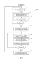
本揭露內容將自實施方式與隨附圖式而得到更完全地理解,其中:圖1係根據本揭露內容繪示的基板處理系統之示例的功能方塊圖,該系統產生視頻信號並使用電腦視覺系統基於視頻信號以偵測殘留膜移除的終點;圖2係根據本揭露內容繪示的用以操作圖1的基板處理系統的方法之示例的流程圖;圖3係根據本揭露內容繪示的基板處理系統之示例的功能方塊圖,其蒐集感測器資料以產生學習模型,電腦視覺系統係使用學習模型以辨別殘留膜移除的終點;圖4~5係根據本揭露內容繪示的產生學習模型以辨別殘留膜移除的終點的方法之示例的流程圖;圖6係根據本揭露內容繪示的使用學習模型以偵測殘留膜移除的終點的方法之示例的流程圖;圖7A係根據本揭露內容繪示的位於處理腔室中並具有便於電腦視覺系統進行終點之偵測的標記的結構之示例的平面圖; 圖7B係根據本揭露內容繪示的位於處理腔室中並具有便於電腦視覺系統進行終點之偵測的標記的結構之示例的側視圖;圖8係根據本揭露內容繪示的使用控制器以最佳化處理條件的系統之示例的功能方塊圖,控制器係連接於多個包括電腦視覺系統的處理控制器;圖9係根據本揭露內容繪示的比較在複數個腔室進行的處理之效能並基於在複數個腔室的處理之效能匹配處理腔室的方法之示例的流程圖;圖10係根據本揭露內容繪示的以元件級別匹配處理腔室的方法之示例的流程圖;圖11A係根據本揭露內容繪示的決定沉積在基板的膜之均勻性的系統的示意圖;圖11B係根據本揭露內容繪示的決定材料是否均勻性地沉積在基板的頂部和底部兩者的系統的示意圖;圖12係根據本揭露內容繪示的決定對元件進行的處理(例如,清潔、蝕刻、沉積等)是否已經均勻性地在整個元件上進行的方法之示例的流程圖;圖13係根據本揭露內容繪示的決定對元件進行的處理(例如,清潔、蝕刻、沉積等)是否已經進行到元件的邊緣上的方法之示例的流程圖;圖14係根據本揭露內容繪示的決定沉積在基板上的膜之均勻性的方法之示例的流程圖;及圖15係根據本揭露內容繪示的決定材料是否均勻性地沉積在基板的頂部和底部兩者的方法之示例的流程圖。 The present disclosure will be more fully understood from the embodiments and accompanying drawings, in which: FIG. 1 is a functional block diagram of an example of a substrate processing system that generates video signals and uses computer vision in accordance with the present disclosure. The system detects the end of residual film removal based on video signals; FIG. 2 is a flowchart of an example of a method for operating the substrate processing system of FIG. 1 according to the present disclosure; FIG. 3 is shown according to the present disclosure. A functional block diagram of an example of a substrate processing system that collects sensor data to generate a learning model that is used by a computer vision system to identify the endpoint of residual film removal; Figures 4-5 are shown in accordance with the disclosure. A flowchart of an example of a method of generating a learning model to identify the endpoint of residual film removal; FIG. 6 is a flowchart of an example of a method of using a learning model to detect the endpoint of residual film removal according to the present disclosure; FIG. 7A is a plan view of an example of a structure located in a processing chamber and having markers that facilitate endpoint detection by a computer vision system in accordance with the present disclosure; 7B is a side view of an example of a structure located in a processing chamber and having markers that facilitate endpoint detection by a computer vision system in accordance with the present disclosure; FIG. 8 is a view of a controller using a controller in accordance with the present disclosure. A functional block diagram of an example of a system for optimizing processing conditions with a controller connected to multiple process controllers including a computer vision system; Figure 9 illustrates a comparison of processing performed in a plurality of chambers in accordance with the present disclosure. Figure 10 is a flowchart of an example of a method of matching process chambers at a device level in accordance with the present disclosure; Figure 11A is a schematic diagram of a system for determining the uniformity of a film deposited on a substrate according to the present disclosure; FIG. 11B is a system for determining whether a material is uniformly deposited on both the top and bottom of a substrate according to the present disclosure. 12 is a flowchart of an example of a method for determining whether processing (eg, cleaning, etching, deposition, etc.) performed on a component has been uniformly performed on the entire component according to the present disclosure; FIG. 13 is a schematic diagram of A flowchart of an example of a method for determining whether processing (eg, cleaning, etching, deposition, etc.) on a component has been performed on the edge of the component, in accordance with the present disclosure; FIG. 14 is a determination in accordance with the present disclosure. 15 is a flowchart of an example of a method for determining whether material is uniformly deposited on both the top and bottom of a substrate in accordance with the present disclosure. .
在圖式中,可重複使用參考數字,以識別相似、及/或相同的元件。 Reference numerals may be repeated in the drawings to identify similar and/or identical elements.
本揭露內容涉及使用電腦視覺系統偵測殘留膜移除之終點的系統和方法。此系統和方法利用安裝在處理腔室外部且與通入處理腔室的窗口相鄰的相機。相機係操作在可見及/或紅外線波長範圍內並產生視頻信號(如本文所用,術語視頻信號亦包括以預定間隔拍攝的一系列之靜止圖像)。藉由電腦視覺系統處理和分析由相機產生的視頻信號,以決定何時達到殘留膜移除的終點。 The present disclosure relates to systems and methods for detecting the endpoint of residual film removal using computer vision systems. This system and method utilizes a camera mounted outside the processing chamber adjacent to a window into the processing chamber. The camera operates in the visible and/or infrared wavelength range and generates a video signal (as used herein, the term video signal also includes a series of still images taken at predetermined intervals). The video signal generated by the camera is processed and analyzed by a computer vision system to determine when the end point of residual film removal is reached.
在一些示例中,終點係基於偵測到的處理腔室中的元件的特徵之變化(例如形狀或邊緣識別、對比度、顏色、亮度或其他特徵)來識別。舉例來說,電腦視覺系統可將從一幀至另一幀中的一或多個特徵的一或多個屬性、在多個幀上的差異、或在幀的滾動式視窗上的差異與一或多個預定門檻值進行比較。在其他示例中,當標記(製作在殘留膜下方的元件上)以足夠的清晰度變為暴露時,終點係受到識別。 In some examples, endpoints are identified based on detected changes in characteristics of components in the processing chamber (eg, shape or edge recognition, contrast, color, brightness, or other characteristics). For example, a computer vision system may compare one or more attributes of one or more features from one frame to another, differences across multiple frames, or differences across a scrolling window of frames from a or multiple predetermined thresholds for comparison. In other examples, the endpoint is identified when the mark (made on the element beneath the residual film) becomes exposed with sufficient clarity.
在一些示例中,電腦視覺系統使用利用視頻信號和化學感測器(例如,吸收感測器或殘餘氣體分析儀感測器)訓練的學習模型(例如,神經網絡或其他深度學習模型)。在學習期間,學習模型識別作為終點的指標之一或多個屬性。一旦學習模型產生後,便不再需要化學感測器。 In some examples, the computer vision system uses a learning model (eg, a neural network or other deep learning model) trained using video signals and chemical sensors (eg, absorption sensors or residual gas analyzer sensors). During learning, the learning model identifies one or more attributes as an endpoint metric. Once the learning model is generated, chemical sensors are no longer needed.
現在參照圖1,其繪示了進行基板處理(例如沉積)的基板處理系統之示例。基板係設置在處理腔室中,且基板處理(例如沉積)係加以執行。該基板被撤移且一或多個其他基板係被處理。久而久之,殘留膜或其他材料積聚在位於處理腔室內的元件(例如,側壁、基板支撐件、氣體分配裝置等)上。清潔係定期進行以移除沉積在處理腔室中的元件上的殘留膜或其他材料。在一示 例中,在清潔期間係使用三氟化氮(NF3)遠距電漿。基板處理系統和處理的具體示例係已繪示和敘述,然可使用其他基板處理系統和處理。舉例來說,在整個本揭露內容中,清潔係僅示例性地敘述為電漿處理。替代地,清潔可為化學處理。舉例來說,取代使用電漿進行清潔,本文所述的清潔可使用三氟化氯(ClF3)進行。當使用化學處理代替電漿進行清潔時,本揭露內容的教示同樣適用。 Referring now to FIG. 1 , illustrated is an example of a substrate processing system that performs substrate processing (eg, deposition). A substrate is disposed in the processing chamber, and substrate processing (eg, deposition) is performed. The substrate is removed and one or more other substrates are processed. Over time, residual film or other material accumulates on components located within the processing chamber (eg, sidewalls, substrate supports, gas distribution devices, etc.). Cleaning is performed periodically to remove residual films or other materials deposited on components in the processing chamber. In one example, nitrogen trifluoride (NF 3 ) remote plasma is used during cleaning. Specific examples of substrate processing systems and processes are shown and described, although other substrate processing systems and processes may be used. For example, throughout this disclosure, cleaning is exemplarily described as plasma treatment only. Alternatively, cleaning may be a chemical treatment. For example, instead of using plasma for cleaning, the cleaning described herein can be performed using chlorine trifluoride (ClF 3 ). The teachings of this disclosure also apply when chemical treatments are used instead of plasma for cleaning.
圖1中的基板處理系統110包括處理腔室112,其包圍基板處理系統110的其他元件並且容納射頻(RF)電漿(如果用於特定的基板處理)。基板處理系統110包括噴淋頭114或其他氣體分配裝置、及基板支撐組件116。基板118係設置在基板支撐組件116上。噴淋頭114引入並分配處理氣體。
若使用電漿,則在基板處理或清潔期間使用的電漿可以是直接或遠距電漿。在一示例中,射頻產生系統130產成射頻電壓並將其輸出到噴淋頭114或基板支撐組件116(另一端是DC接地、AC接地或浮接)。僅作為示例,射頻產生系統130可包括產生射頻電壓的射頻電壓產生器132,射頻電壓由匹配網路134饋送到噴淋頭114或基板支撐組件116。在一些示例中,原位電漿係在基板處理期間使用,且遠距電漿係在清潔期間輸送。
If plasma is used, the plasma used during substrate processing or cleaning may be direct or remote plasma. In one example,
氣體輸送系統140包括一或多個氣體源142-1、142-2、...和142-N(統稱為氣體源142),其中N是大於零的整數。氣體源142將一或多種蝕刻氣體混合物、前驅物氣體混合物、清潔氣體混合物、灰化氣體混合物等供應至處理腔室112。蒸發的前驅物亦可被使用。氣體源142藉由閥144-1、144-2、...和144-N(統稱為閥144)和質量流量控制器146-1、146-2、...和146-N(統稱為質量流量控制器146)連接至歧管148。歧管148的輸出係饋送至處理腔室112。僅作為示例,歧管148的輸出係饋送至噴淋頭114。
The
加熱器150可連接至設置在基板支撐組件116中的加熱線圈(未繪示)。加熱器150可用以控制基板支撐組件116和基板118的溫度。閥160和幫浦162可用以排空處理腔室112的反應物。控制器170可用以控制基板處理系統110的元件。僅舉例來說,控制器170可用以控制下述:處理氣體的流動、監控處理參數(例如,溫度、壓力、功率等)、激發和熄滅電漿、移除反應物等等。
The
處理腔室112包括位於處理腔室112的一或多個表面上的一或多個窗口172。一或多個相機174產生基板支撐組件116、基板或其他腔室元件的視頻信號。
控制器170包括電腦視覺系統180,其接收來自相機174的一或多個視頻信號。電腦視覺系統180基於視頻信號識別殘留膜移除的終點。雖然係繪示了單一相機174,然可使用一或多個其他相機174。在一些示例中,相機定位裝置182調整相機174的位置以改變相機174的視野。在一些示例中,控制器170可用以在偵測殘留膜移除的終點之前、期間或之後改變相機174的位置。在一些示例中,一或多個濾波器設置在相機174和處理腔室之間以過濾一或多個波長或波長範圍。
The
在一些示例中,電腦視覺系統180決定視頻的視覺特性之差異以識別殘留膜移除的終點。舉例來說,電腦視覺系統180可比較從一幀到另一幀的顏色、亮度及/或對比度水平、在多個幀上的差異、或是在多個幀的滾動視窗(rolling window)上的差異。
In some examples,
在其他示例中,電腦視覺系統180藉由充分識別位於處理腔室中的一或多個元件上的標記來偵測殘留膜移除的終點。當在清潔期間從一或多
個元件移除殘留膜時,特性(例如標記的邊緣、顏色、圖案及/或整體形狀)將變得更清楚。擷取的影像可使用關聯函數來跟預定影像進行比較。當計算的關聯值超過預定門檻值時,可觸發檢出。終點可在預定事件發生時決定,或是預定事件可用來啟動計時器,且終點可在計時器啟動之後被宣告。
In other examples, the
在其他示例中,學習模型係可使用化學感測器(例如吸收感測器或殘餘氣體分析儀感測器)和視頻信號來訓練。一旦經過訓練,學習模型便基於視頻信號偵測終點且不需要使用化學感測器,如下面將進一步描述的。 In other examples, the learning model can be trained using a chemical sensor (such as an absorption sensor or a residual gas analyzer sensor) and a video signal. Once trained, the learning model detects endpoints based on the video signal and does not require the use of a chemical sensor, as described further below.
現在參照圖2,其繪示了使用視頻信號和電腦視覺系統來偵測殘留膜移除的終點之方法200。在步驟202,若基板需要進行處理,則方法繼續執行步驟203。在步驟203,基板被裝載到處理腔室中並進行基板處理(例如沉積)。
Referring now to FIG. 2 , a method 200 is shown for detecting the end point of residual film removal using a video signal and a computer vision system. At
在步驟204,在進行基板處理之後將基板從處理腔室撤移。在步驟206,方法決定腔室是否需要清潔。若步驟206為否,則方法返回步驟202。若步驟206為是,則方法繼續執行步驟208並提供遠距電漿(或將氣體混合物供應到處理腔室並激發電漿)。若使用原位電漿,則可在視頻相機和處理腔室之間設置濾波器。
At
在步驟210,在清潔處理的期間產生視頻信號。在步驟212,電腦視覺系統進行視頻信號的視頻分析。在步驟214,電腦視覺系統處理視頻信號並偵測膜移除的終點。在步驟216,方法決定是否已偵測到終點。若步驟216為否,則方法返回步驟210。當步驟216為是,方法繼續執行步驟218並停止供應遠距電漿(或者熄滅電漿並關閉電漿氣體混合物)。方法繼續從步驟218回到步驟202。
At
現在參照圖3,學習模型係可產生並用以偵測殘留膜移除的終點。建模模組220產生由電腦視覺系統180使用的學習模型。學習模型係基於包括視頻信號的訓練資料和化學感測器230(例如吸收感測器或殘餘氣體分析儀感測器)的輸出來產生。雖然繪示了特定位置,但化學感測器可設置在其他位置,例如排氣裝置。雖然建模模組220係繪示位於控制器170中,但建模模組220可在模型產生期間位於另一電腦(未繪示)中,且模型可被傳送至及/或儲存在控制器170。
Referring now to Figure 3, a learning model can be generated and used to detect the endpoint of residual film removal.
建模模組220使用多組訓練資料來識別視頻信號中的作為終點之指標的特徵。在一些示例中,多組訓練資料儲存在本地或遠端資料庫224中。一旦產生學習模型,學習模型便可載入到控制器170中(如標號228所示)且不再需要化學感測器230。
The
在一些示例中,學習模型包括從由線性模型(linear model)、支援向量機模型(support vector machine model)、決策樹模型(decision tree model)、隨機森林模型(random forest model)和高斯模型(Gaussian model)組成的群組中選擇的監督式學習模型。然而,本揭露內容不限於監督式學習。另外或替代地,可使用無監督式學習。在其他示例中,學習模型採用主成分分析(principal component analysis,PCA)、神經網絡、自動編碼、回歸分析及/或偏最小平方(partial least squares,PLS)。舉例來說,神經網絡可利用卷積神經網絡(convolutional neural network,CNN)、遞迴神經網絡(recurrent neural network,RNN)、強化學習(reinforcement learning)(基於獎勵的模型)及/或其他方法。 In some examples, the learning model includes a linear model, a support vector machine model, a decision tree model, a random forest model, and a Gaussian model. A supervised learning model selected from a group consisting of models. However, this disclosure is not limited to supervised learning. Additionally or alternatively, unsupervised learning can be used. In other examples, the learning model uses principal component analysis (PCA), neural networks, autoencoding, regression analysis, and/or partial least squares (PLS). For example, the neural network may utilize a convolutional neural network (CNN), a recurrent neural network (RNN), reinforcement learning (reward-based model), and/or other methods.
現在參照圖4~5,其繪示了產生用於電腦視覺的學習模型以識別殘留膜移除的終點的方法。用以產生用於產生學習模型(由電腦視覺系統使用以偵測殘留膜移除的終點)的訓練資料之方法400係被繪示。在步驟404,方法決定基板是否需要進行處理。若步驟404為是,則方法繼續執行步驟408。在步驟408,基板係被裝載到處理腔室中並進行基板處理(例如沉積)。
Referring now to Figures 4-5, illustrated are methods for generating a learning model for computer vision to identify the endpoint of residual film removal. A
在步驟412,在進行基板處理之後將基板從處理腔室撤移。在步驟416,方法決定腔室是否需要清潔。若步驟416為否,則方法返回步驟408。若步驟416為是,則在步驟422,方法提供遠距電漿或將氣體混合物供應至處理腔室並激發電漿。在步驟430,方法產生並儲存在處理腔室中的一或多個結構之視頻信號。在步驟434,方法產生並儲存由化學感測器產生的化學感測器資料。在步驟438,使用化學感測器偵測殘留膜移除的終點。在步驟440,方法決定殘留膜是否被移除。若步驟440為否,則方法返回步驟430。若步驟440為是,則方法繼續執行步驟444並停止供應遠距電漿(或熄滅電漿並關閉電漿氣體混合物)。
In
在圖5中,其繪示將在圖4中產生的訓練資料轉換為學習模型之方法450。在步驟454,方法決定是否已經收集了足夠數量的訓練樣本。在步驟458,方法產生將視頻信號與由化學感測器決定的殘留膜移除的終點相關聯的學習模型。在步驟462,模型係儲存在控制器中以供清潔處理。在步驟466,控制器使用學習模型基於視頻(或一系列的靜止圖像)來識別用於移除殘留膜的終點,而不使用化學感測器(例如吸收感測器或殘餘氣體分析儀感測器)。
In FIG. 5 , a
現在參照圖6,其繪示了使用視頻信號和具有學習模型的電腦視覺系統以偵測殘留膜移除的終點之方法500。在步驟502,若基板需要進行處理,則方法繼續執行步驟503。在步驟503,基板係被裝載至處理腔室中並進行基板處理(例如沉積)。
Referring now to Figure 6, illustrated is a
在步驟504,在進行基板處理之後將基板從處理腔室撤移。在步驟506,方法決定腔室是否需要清潔。若步驟506為否,則方法返回步驟503。若步驟506為是,則方法繼續執行步驟508並提供遠距電漿(或將氣體混合物供應至處理腔室並激發電漿)。若使用原位電漿,則可在視頻相機和處理腔室之間設置濾波器。
At
在步驟510,在清潔處理之期間產生視頻信號。在步驟512,電腦視覺系統使用學習模型進行視頻信號的視頻分析。在步驟514,電腦視覺系統使用學習模型和視頻信號偵測膜移除的終點。在步驟516,方法決定是否已偵測到終點。若步驟516為否,則方法返回步驟510。當步驟516為真,方法繼續執行步驟518並且停止供應遠距電漿(或者熄滅電漿並關閉電漿氣體混合物)。方法繼續從步驟518回到步驟502。
At
現在參照圖7A~7B,其繪示標記之示例,該等標記位於設置在處理腔室中的結構上以便於偵測殘留膜移除的終點。在圖7A中,結構480包括一或多個標記494-1、494-2、...和494-Z,其中Z是大於零的整數。在一些示例中,標記可具有不同的圖案、陰影、顏色或其他設計,以提高於電腦視覺系統偵測期間的準確度。在一些示例中,結構480對應於基板支撐件的上表面,如圖7A所示。在其他示例中,結構480對應於基板支撐件的側面,如圖
7B所示。可理解的是,其他元件(例如氣體分配裝置、支撐件、側壁等的)亦可由類似的方式加以標記。
Referring now to Figures 7A-7B, illustrated are examples of markers placed on structures disposed in a processing chamber to facilitate detection of endpoints of residual film removal. In Figure 7A,
現在參照圖8,電腦視覺系統及/或學習模型可用以最佳化處理參數,例如氣流、氣體物種、氣體成分或其他參數。最佳化系統600包括控制器620,控制器620包括處理最佳化模組624,處理最佳化模組624包括學習模組626。控制器620與一或多個處理部630-1、630-2、...和630-Y(其中Y是大於零的整數)進行通訊。每個處理部包括控制器638-1、638-2、...和638-Y,其分別包括電腦視覺系統640-1、640-2、...和640-Y。在一些示例中,部分的電腦視覺系統640-1、640-2、...和640-Y中可更包括學習模型650-1、650-2、...和650-Y。處理最佳化模組624接收多個訓練集,訓練集包括處理條件和來自控制器638-1、638-2、...和638-Y的結果。處理最佳化模組624使用藉由學習模組626實現的學習模型、神經網絡或人工智慧來最佳化每一個控制器638-1、638-2、...和638-Y的處理條件。
Referring now to FIG. 8 , a computer vision system and/or a learning model may be used to optimize a process parameter, such as airflow, gas species, gas composition, or other parameter. The
用以偵測殘留膜移除的終點之系統和方法識別處理腔室中的一或多個元件的表面上的特徵,以使用便宜的相機決定處理腔室的清潔狀態。在足夠的訓練資料之後,神經網路(深度學習)模型係用以改變清潔處理參數(例如壓力、流量、基座位置等)使得腔室與腔室清潔效能匹配。 Systems and methods for detecting endpoints of residual film removal identify features on the surface of one or more components in a processing chamber to determine the cleaning status of the processing chamber using an inexpensive camera. After sufficient training data, the neural network (deep learning) model is used to change the cleaning process parameters (such as pressure, flow rate, base position, etc.) to match the chamber to chamber cleaning performance.
本揭露內容的系統和方法可用於在單一工具或多個工具中橫跨多個處理腔室比較一處理(例如,清潔處理、蝕刻處理、沉積處理等)之效能。一般來說,用於特定處理(例如蝕刻或沉積處理)的處理腔室具有類似的設計。因此,在這些處理腔室中進行的處理(例如,清潔、蝕刻、沉積等)期望具有類似的效能(例如,類似的運行時間)。也就是說,兩個相同的處理腔 室應以相同的方式進行相同的處理。換句話說,在兩個類似設計的處理腔室中相同的處理之效能也應該是類似的。當在這些腔室中進行處理時,本揭露內容的系統和方法可分析從類似設計的處理腔室收集的資料。然後,系統和方法可基於分析決定處理的效能是否在處理腔室之間是相似的(亦即,若處理腔室是匹配的且以相同的方式進行處理)。 The systems and methods of the present disclosure can be used to compare the performance of a process (e.g., a cleaning process, an etching process, a deposition process, etc.) across multiple processing chambers in a single tool or multiple tools. Generally, processing chambers used for a particular process (e.g., an etching or deposition process) have similar designs. Therefore, the processes (e.g., cleaning, etching, deposition, etc.) performed in these processing chambers are expected to have similar performance (e.g., similar run times). That is, two identical processing chambers should perform the same process in the same manner. In other words, the performance of the same process in two similarly designed processing chambers should also be similar. The systems and methods of the present disclosure can analyze data collected from similarly designed processing chambers while the processes are performed in these chambers. The systems and methods can then determine based on the analysis whether the performance of the process is similar between process chambers (i.e., if the process chambers are matched and process in the same manner).
進一步來說,分析可幫助決定元件級別的處理效能。舉例來說,在清潔處理的情況下,分析可幫助決定藉由清潔處理清潔特定元件所花費的時間是否在多個類似設計的處理腔室中是相同的。此決定可另外決定對每個處理腔室進行清潔處理的總運行時間是否相同。 Further, analysis can help determine component-level process performance. For example, in the case of a cleaning process, analysis can help determine whether the time it takes to clean a particular component via a cleaning process is the same across multiple similarly designed process chambers. This determination can additionally determine whether the total run time for the cleaning process is the same for each process chamber.
可進行類似的分析以比較其他處理(例如,沉積和蝕刻處理)在多個處理腔室間的的效能。基於比較,特定腔室中的處理之效能的任何異常可被偵測出來,且異常的原因可被校正。舉例來說,包括多個處理腔室的工具中的一處理腔室可能比工具中的其他處理腔室更快地被清潔。對所述處理腔室的清潔處理應較早停止以防止損壞所述處理腔室。如果繼續進行清潔處理,則該處理腔室可能會損壞。然而,如果多個工具上的多個處理腔室表現出不同的清潔時間,則這些處理腔室的不同清潔時間可指示需要對這些處理腔室進行設計改變以實現腔室匹配。類似的分析可對其他處理(例如,沉積和蝕刻處理)進行以實現腔室匹配。 Similar analyzes can be performed to compare the performance of other processes (eg, deposition and etch processes) across multiple process chambers. Based on the comparison, any anomalies in the performance of the process in a particular chamber can be detected and the cause of the anomaly corrected. For example, one processing chamber in a tool that includes multiple processing chambers may be cleaned faster than other processing chambers in the tool. The cleaning process of the processing chamber should be stopped early to prevent damage to the processing chamber. If the cleaning process continues, the processing chamber may be damaged. However, if multiple process chambers on multiple tools exhibit different cleaning times, the different cleaning times for the process chambers may indicate that design changes to the process chambers are needed to achieve chamber matching. Similar analysis can be performed on other processes (eg, deposition and etch processes) to achieve chamber matching.
本揭露內容的系統和方法可用於決定對於處理(例如,沉積和蝕刻處理)的各種效能衡量指標。舉例來說,效能衡量指標可包括整個晶圓的蝕刻之均勻性、整個晶圓的沉積之均勻性、整個晶圓的溫度之均勻性等等。舉例來說,膜厚度的均勻性可在膜沉積以及如下所述的膜移除的期間被決定出 來。值得注意的是,系統和方法可於原位(亦即,在處理之後不用將晶圓從處理腔室撤移到單獨的量測室以做出這些決定)且即時地(亦即,當晶圓正在進行處理時)做出這些決定。 The systems and methods of the present disclosure can be used to determine various performance metrics for processes (eg, deposition and etch processes). For example, performance metrics may include etch uniformity across the wafer, deposition uniformity across the wafer, temperature uniformity across the wafer, etc. For example, film thickness uniformity can be determined during film deposition and film removal as described below Come. Notably, the systems and methods can make these decisions in situ (i.e., without removing the wafer from the processing chamber to a separate metrology chamber after processing) and on the fly (i.e., when the wafer is processed) These decisions are made while the circle is being processed).
舉例來說,在從晶圓移除膜的期間,系統和方法在膜變薄時可使用例如光干涉的技術來整體地對膜進行觀察,並決定膜是否被完全移除,整個晶圓上的移除是否均勻等等。舉例來說,考慮從晶圓上移除氧化銅膜。銅在氧化時會改變顏色。因此,在移除氧化銅的期間,本揭露內容的系統和方法在氧化銅正被移除且純銅被暴露時可觀察到從整個晶圓反射的光之波長的變化。波長的變化可指示氧化銅移除的狀態。使用光學濾波器,系統和方法可在局部的晶圓上和整個晶圓上觀察變化。 For example, during the removal of a film from a wafer, the systems and methods can use techniques such as optical interferometry to observe the film as a whole as it thins and determine whether the film is completely removed, whether the removal is uniform across the wafer, etc. For example, consider removing a copper oxide film from a wafer. Copper changes color when oxidized. Therefore, during the removal of copper oxide, the systems and methods of the present disclosure can observe changes in the wavelength of light reflected from the entire wafer as the copper oxide is being removed and pure copper is exposed. The change in wavelength can indicate the status of the copper oxide removal. Using optical filters, the systems and methods can observe changes locally on the wafer and across the entire wafer.
在不具觀察整個晶圓的能力之情況下,僅可觀察晶圓上的單一點,而基於觀察晶圓上的單一點可能得出關於從整個晶圓上膜移除的錯誤結論。舉例來說,假設僅有晶圓的中心被觀察並做出氧化銅從中心移除的決定。在不具觀察整個晶圓的能力之情況下,儘管晶圓的邊緣仍有部分氧化銅未被移除,可能得出氧化銅已從整個晶圓上移除之錯誤的結論。相反地,在具有觀察整個晶圓的能力的情況下,本揭露內容的系統和方法可偵測晶圓的中心的膜是否以比晶圓邊緣的膜更快的速率移除以及膜是否從整個晶圓上移除。此外,這些決定是於原位做出的。 Without the ability to observe the entire wafer, only a single point on the wafer can be observed, and erroneous conclusions may be drawn about film removal from the entire wafer based on observing a single point on the wafer. For example, assume that only the center of the wafer is viewed and a decision is made that copper oxide is removed from the center. Without the ability to observe the entire wafer, it may be possible to incorrectly conclude that copper oxide has been removed from the entire wafer even though there is still some copper oxide at the edge of the wafer. Conversely, with the ability to observe the entire wafer, the systems and methods of the present disclosure can detect whether the film in the center of the wafer is removed at a faster rate than the film at the edge of the wafer and whether the film is removed from the entire wafer. removed from the wafer. Furthermore, these decisions are made in situ.
在另一示例中,當在晶圓上生長膜時,由於成核延遲(nucleation delay),膜通常需要花費時間來生長。由於具有觀察整個晶圓的能力,本揭露內容的系統和方法可偵測膜生長在一部分的晶圓上之前是否在晶圓的另一部分上生長。舉例來說,可使用紫外線濾波器在整個晶圓上觀察膜生 長(亦即,由於生長引起的膜厚度之變化)。此外,可使用紅外線濾波器觀察晶圓的溫度和其中的變化。使用兩個濾波器(紫外線和紅外線)進行的兩個觀察(膜厚度和晶圓溫度)可求取相關性以決定在整個晶圓上的膜生長之均勻性。值得注意的是,此決定是在處理腔室中於原位且即時進行的,而無需將晶圓撤移到單獨的量測室。 In another example, when growing a film on a wafer, the film generally takes time to grow due to nucleation delay. With the ability to observe the entire wafer, the systems and methods of the present disclosure can detect if a film grows on one portion of the wafer before growing on another portion of the wafer. For example, a UV filter can be used to observe film growth (i.e., changes in film thickness due to growth) across the wafer. Additionally, an IR filter can be used to observe the temperature of the wafer and changes therein. The two observations (film thickness and wafer temperature) made using the two filters (UV and IR) can be correlated to determine the uniformity of film growth across the wafer. Notably, this decision is made in situ and instantly in the processing chamber, without the need to evacuate the wafer to a separate metrology room.
此外,本揭露內容的系統和方法可監控晶圓的邊緣。舉例來說,藉由將相機聚焦在晶圓的上邊緣上,系統和方法可決定是否已將晶圓處理(例如,清潔、蝕刻等)達晶圓的邊緣。同樣地,這是在原位而不是在將晶圓撤移到單獨的量測室之後完成的。在晶圓進行處理的同時監控晶圓邊緣的這種能力,可在基於觀察邊緣並做出處理已完成至晶圓的邊緣的決定時立刻中斷處理,藉以幫助節省處理時間和處理材料。 Additionally, the systems and methods of the present disclosure can monitor the edge of a wafer. For example, by focusing the camera on the upper edge of the wafer, systems and methods can determine whether the wafer has been processed (eg, cleaned, etched, etc.) to the edge of the wafer. Again, this is done in situ rather than after removing the wafers to a separate metrology chamber. The ability to monitor the wafer edge while the wafer is being processed can help save processing time and processing materials by immediately interrupting processing based on observing the edge and making a decision that processing is complete to the edge of the wafer.
此外,在一些例子中,可在晶圓的上表面和下表面兩者上進行沉積。本揭露內容的系統和方法可用於觀察晶圓的上表面和下表面兩者的沉積處理。舉例來說,光纖探針及/或顯微鏡頭可與本揭露內容的系統和方法結合使用,以觀察晶圓底部的大面積並獲得其影像。在一些例子中,一或多個發光二極體可安裝在處理腔室中以照亮晶圓的底部。擷取的影像可進行處理和分析以決定整個晶圓底部的沉積之均勻性。舉例來說,處理後的影像可與實際量測的沉積水平(量測已於先前進行)求取相關性,然後該相關性可用來於原位推斷沉積水平和均勻性。 Additionally, in some examples, deposition can be performed on both the upper and lower surfaces of the wafer. The systems and methods of the present disclosure may be used to observe deposition processes on both the upper and lower surfaces of a wafer. For example, fiber optic probes and/or microscope heads may be used in conjunction with the systems and methods of the present disclosure to observe and image large areas of the bottom of a wafer. In some examples, one or more light emitting diodes may be installed in the processing chamber to illuminate the bottom of the wafer. The captured images can be processed and analyzed to determine deposition uniformity across the entire wafer bottom. For example, the processed images can be correlated with actual measured deposition levels (measurements have been taken previously), and this correlation can then be used to infer deposition levels and uniformity in situ.
本揭露內容的系統和方法亦可用於量測處理腔室中的噴淋頭和基座之間的間隙。舉例來說,兩個相機可分別聚焦在噴淋頭和基座上,而來自兩個相機的視頻信號可用以決定噴淋頭和基座之間的距離。然後可使用量測來 控制(改變)噴淋頭和基座之間的間隙(例如,藉由控制使基座相對於噴淋頭移動的裝置)。 The systems and methods of the present disclosure may also be used to measure the gap between a showerhead and a base in a processing chamber. For example, two cameras can focus on the sprinkler head and the base, respectively, and the video signals from both cameras can be used to determine the distance between the sprinkler head and the base. Measurements can then be used to Control (change) the gap between the sprinkler head and the base (e.g., by controlling a device that moves the base relative to the sprinkler head).
此外,在一些處理腔室中,在電漿已經熄滅之後,寄生電漿可能殘留在處理腔室中。寄生電漿是不符合要求的且難以偵測。本揭露內容的系統和方法的相機可用以偵測寄生電漿。本揭露內容的系統和方法的許多其他應用可受到構思,且屬於本揭露內容之範疇。 Additionally, in some processing chambers, parasitic plasma may remain in the processing chamber after the plasma has been extinguished. Parasitic plasma is undesirable and difficult to detect. The cameras of the systems and methods of the present disclosure may be used to detect parasitic plasma. Many other applications of the systems and methods of the present disclosure may be contemplated and are within the scope of the present disclosure.
圖9係根據本揭露內容繪示了用於腔室匹配的方法700。清潔處理僅用以示例。方法700的教示亦可與沉積或蝕刻處理一起使用。在步驟702,方法700開始清潔處理以清潔多個腔室。在步驟704,方法700收集與清潔多個腔室相關聯的資料。在步驟706,方法700分析收集的資料。在步驟708,方法700決定來自多個腔室之一者的資料是否異常。舉例來說,方法700決定多個腔室之一者是否比該多個腔室之其餘腔室具有更短的清潔處理之運行時間(亦即,清潔更快)。在步驟710,若偵測到異常,則方法700決定與多個腔室之一者相關聯之異常的一或多個原因。在步驟712,方法700校正異常的一或多個原因。之後,或是若在步驟708未偵測到異常,則在步驟714,方法700決定所有腔室是否為潔淨的或是清潔處理是否應該繼續(亦即,清潔處理是否尚未完成)。若並非所有腔室皆為潔淨的(亦即,清潔處理還不應終止),則方法700返回步驟702。
FIG. 9 illustrates a
圖10係根據本揭露內容繪示了用於以元件級別匹配處理腔室的方法750。同樣,清潔處理僅用以示例。方法750的教示亦可與沉積或蝕刻處理一起使用。在步驟752,方法750開始清潔處理以清潔多個腔室。在步驟754,方法750收集與清潔多個腔室相關聯的資料。在步驟756,方法750分析
收集的資料。在步驟758,方法750決定多個腔室之一者的元件是否在於其他腔室的同一元件變得清潔之前(亦即,較快)變得清潔。在步驟760,若多個腔室之一者的元件在於其他腔室的同一元件變得清潔之前(亦即,較快)變得清潔,則方法750停止所述腔室的清潔處理。之後,或是多個腔室之一者的元件並未在於其他腔室的同一元件變得清潔之前(即,較快)變得清潔,則在步驟762,方法750決定所有腔室是否為潔淨的或者是清潔處理是否應該繼續(亦即,若清潔處理尚未完成)。若並非所有腔室皆為清潔的(亦即,若清潔處理還不應終止),則方法750返回步驟752。
Figure 10 illustrates a
圖11A係根據本揭露內容繪示用以決定沉積在基板上的膜之均勻性的系統800之示意圖。系統800包括處理腔室112,其對基板118進行處理(例如,沉積材料在其上)。處理腔室112包括窗口172。系統800包括控制器170,其包括電腦視覺系統180、相機174和相機定位裝置182。
11A is a schematic diagram of a
系統800還包括紫外線濾波器806和紅外線濾波器808。紫外線濾波器806和紅外線濾波器808設置在照相機174和窗口172之間。紫外線濾波器806過濾從基板118並經由窗口172接收的紫外光之波長。紅外線濾波器808過濾從基板118並經由窗口172接收的紅外光之波長。
電腦視覺系統180接收紫外線濾波器806和紅外線濾波器808的輸出。電腦視覺系統180基於紫外線濾波器806的輸出決定沉積在基板118上的多個位置處的材料之厚度。電腦視覺系統180基於紅外線濾波器808的輸出決定基板118上多個位置處的溫度。電腦視覺系統180將厚度的決定和溫度的決定相關聯,並基於該相關性決定在整個基板118上沉積的均勻性。
圖11B係根據本揭露內容繪示用於決定材料是否均勻地沉積在基板的頂部和底部兩者的系統850之示意圖。系統850包括處理腔室999,其對基板804的上側和下側(由箭頭標識)兩者進行處理(例如,沉積材料在其上)。處理腔室999包括窗口172。在基板804的兩側沉積材料的細節(例如,使用CVD)與本揭露內容無關因此並未繪示和描述。系統850包括控制器170,控制器170包括電腦視覺系統180、相機174和相機定位裝置182。
11B is a schematic diagram of a
系統850更包括光學感測器810(例如,光纖感測器或微透鏡)以觀察基板804的底部。感測器定位裝置812將光學感測器810定位成指向基板804的底部的各個位置。
The
電腦視覺系統180將相機174聚焦在基板804的頂部。電腦視覺系統180從相機174接收基板804的頂部的影像。電腦視覺系統180將光學感測器810定位以觀察基板804的底部。電腦視覺系統180從光學感測器810接收基板804的底部的影像。電腦視覺系統180處理從相機174和光學感測器810接收的影像。電腦視覺系統180基於從相機174和光學感測器810接收的影像之處理來決定基板804的整個頂部和整個底部的沉積之均勻性。
The
圖12係根據本揭露內容繪示用於決定在元件上進行的處理(例如,清潔、蝕刻、沉積等)是否已經在整個元件上均勻地進行的方法900。在步驟902,方法900過濾從元件(例如,晶圓)並經由處理腔室(該元件於其中進行處理)上提供之窗口接收的光的一或多個波長。在步驟904,方法900基於使用光干涉的過濾來決定元件的狀態。在步驟906,方法900基於元件的狀態決定處理是否已經在整個元件上均勻地進行。在步驟908,若處理已經在
整個元件上均勻地進行,則方法900終止處理。若處理尚未在整個元件上均勻地進行,則方法900返回步驟902。
Figure 12 illustrates a
圖13係根據本揭露內容繪示用以決定對元件進行的處理(例如,清潔、蝕刻、沉積等)是否已經進行到元件的邊緣的方法920。在步驟922,方法920將相機聚焦在元件(例如,晶圓)的邊緣上。在步驟924,方法920決定處理是否已經完成達元件的邊緣。在步驟926,若處理已經完成達元件的邊緣,則方法920終止處理。若處理尚未完成達元件的邊緣,則方法920返回步驟922。
FIG. 13 illustrates a
圖14係根據本揭露內容繪示用於決定沉積在基板上的膜之均勻性的方法940。在步驟942,方法940使用如參考圖11A所解釋的紫外線濾波器量測整個基板的膜之厚度。在步驟944,方法940使用如參考圖11A所解釋的紅外線濾波器量測整個基板上的溫度。在步驟946,方法940將厚度和溫度量測值相關聯。在步驟948,方法940基於量測值決定膜是否已均勻地沉積在整個基板上。在步驟950,若膜已經均勻地沉積在整個基板上,則方法940終止沉積處理。若膜尚未均勻地沉積在整個基板上,則方法940返回步驟942。
FIG. 14 illustrates a
圖15係根據本揭露內容繪示用於決定材料是否均勻地沉積在基板的頂部和底部兩者的方法960。在步驟962,方法960使用如參考圖11B所述的相機觀察基板的頂部。在步驟964,方法960使用如參考圖11B所述的一或多個光學感測器觀察基板的底部。在步驟966,方法960決定膜是否均勻地沉積在整個基板的頂部和底部上,如參考圖11B所述。在步驟968,若膜已經均勻地沉積在整個基板的頂部和底部上,則方法960終止沉積處理。若膜尚未均勻地沉積在整個基板的頂部和底部上,則方法960返回步驟962。
FIG. 15 illustrates a
為清楚起見,上述方法分開描述。一種或多種上述方法可以全部或部分組合,並且可以一起進行。 For clarity, the above methods are described separately. One or more of the above methods may be combined in whole or in part and may be performed together.
先前描述在本質上僅為說明性的,而非意圖限制本揭露內容、其應用、或用途。本揭露內容之廣泛教示可以各種形式實施。因此,雖本揭露內容包括特定範例,然由於當研究圖式、說明書、與以下申請專利範圍時,其他變化將變得顯而易見,故本揭露內容之真實範疇不應如此受限。應理解,在不改變本揭露內容之原理的情形下,方法中之一或更多步驟可以不同次序(或同時)執行。再者,雖實施例之每一者係於以上描述為具有某些特徵,然關於本揭露內容之任何實施例所述該等特徵之任何一或更多者可在任何其他實施例中實施、及/或與其特徵組合(即使並未明確描述該組合)。換言之,所述實施例並非相互排斥,且一或更多實施例彼此的置換維持在本揭露內容之範疇中。 The preceding description is merely illustrative in nature and is not intended to limit the disclosure, its application, or uses. The broad teachings of this disclosure can be implemented in a variety of forms. Therefore, while this disclosure includes specific examples, the true scope of this disclosure should not be so limited, since other variations will become apparent upon studying the drawings, specification, and scope of the following claims. It should be understood that one or more steps in the method may be performed in a different order (or simultaneously) without changing the principles of the present disclosure. Furthermore, although each of the embodiments is described above as having certain features, any one or more of the features described with respect to any embodiment of the present disclosure may be implemented in any other embodiment. and/or in combination with its characteristics (even if the combination is not explicitly described). In other words, the embodiments are not mutually exclusive, and substitutions of one or more embodiments for each other remain within the scope of the present disclosure.
元件(例如,在模組、電路元件、半導體疊層等)之間的空間與功能上的關係乃使用包括「連接」、「接合」、「耦合」、「鄰近」、「在...旁」、「在...之上」、「上方」、「下方」、與「設置」之各種術語描述。除非明確地描述為「直接」之情形下,否則當於上述揭露內容中描述第一與第二元件之間的關係時,該關係可為在第一與第二元件之間不存在其它中介元件之直接關係,但亦可為在第一與第二元件之間存在一或更多中介元件(空間上或功能上)的間接關係。如本文所用,詞組「A、B、與C之至少一者」應解釋成意指使用非排除性邏輯OR之邏輯(A OR B OR C),且不應解釋成代表「A之至少一者、B之至少一者、與C之至少一者」。 The spatial and functional relationships between components (e.g., in modules, circuit components, semiconductor stacks, etc.) are defined using terms including "connected," "joined," "coupled," "proximate," "next to... ”, “above”, “above”, “below”, and “set”. Unless explicitly described as "direct," when a relationship between a first and a second element is described in the above disclosure, the relationship may be such that there are no other intervening elements between the first and the second element. The relationship may be a direct relationship, but it may also be an indirect relationship where one or more intermediary elements (spatially or functionally) exist between the first and second elements. As used herein, the phrase "at least one of A, B, and C" shall be construed to mean the logic of OR using the non-exclusive logical OR (A OR B OR C), and shall not be construed to mean "at least one of A , at least one of B, and at least one of C."
在一些實施例中,控制器為系統的一部分,該系統可為以上描述範例的一部分。如此之系統可包含半導體處理設備,該半導體處理設備包含 (複數)處理工具、(複數)腔室、(複數)處理用平台、及/或特定的處理元件(基板基座、氣體流動系統等)。該等系統可與電子設備整合,以在半導體晶圓或基板的處理之前、期間、以及之後,控制該等系統的運作。電子設備可稱為「控制器」,其可控制系統或複數系統的諸多元件或子元件。取決於處理需求及/或系統類型,控制器可程式設計成控制本文中所揭露之製程的任何者,包含處理氣體的傳送、溫度設定(例如,加熱及/或冷卻)、壓力設定、真空設定、功率設定、射頻(RF)產生器設定、RF匹配電路設定、頻率設定、流速設定、流體傳送設定、位置和操作設定、基板轉移(進出與特定系統相連接或相接合之工具及其他轉移工具、及/或裝載鎖)。 In some embodiments, the controller is part of a system that may be part of the examples described above. Such a system may include semiconductor processing equipment including (Plural) processing tools, (plural) chambers, (plural) processing platforms, and/or specific processing elements (substrate pedestals, gas flow systems, etc.). These systems may be integrated with electronic equipment to control the operation of the systems before, during, and after processing of semiconductor wafers or substrates. An electronic device, called a "controller," controls a system or components or subcomponents of a system. Depending on the processing needs and/or system type, the controller may be programmed to control any of the processes disclosed herein, including the delivery of process gases, temperature settings (e.g., heating and/or cooling), pressure settings, vacuum settings , power settings, radio frequency (RF) generator settings, RF matching circuit settings, frequency settings, flow rate settings, fluid delivery settings, position and operation settings, substrate transfer (in and out of tools connected or interfaced with specific systems and other transfer tools , and/or load lock).
廣泛地講,控制器可界定為具有用以接收指令、發佈指令、控制操作、啟動清洗操作、啟動終點量測以及類似者之諸多積體電路、邏輯、記憶體、及/或軟體的電子設備。積體電路可包含:儲存程式指令之韌體形式的晶圓、數位訊號處理器(DSP,digital signal processor)、界定為特殊用途積體電路(ASIC,application specific integrated circuit)的晶圓、及/或一或更多微處理器、或執行程式指令(例如,軟體)的微控制器。程式指令可為以不同的單獨設定(或程式檔案)之形式而傳達至控制器或系統的指令,該單獨設定(或程式檔案)為實行特定的製程(在半導體基板上,或針對半導體基板)界定操作參數。在一些實施例中,操作參數可為由製程工程師為了在一或更多以下者的製造期間實現一或更多處理步驟而界定之配方的一部分:覆層、材料、金屬、氧化物、矽、二氧化矽、表面、電路、及/或基板的晶粒。 Broadly speaking, a controller may be defined as an electronic device having integrated circuits, logic, memory, and/or software for receiving instructions, issuing instructions, controlling operations, initiating cleaning operations, initiating endpoint measurements, and the like. The integrated circuits may include: a wafer in the form of firmware storing program instructions, a digital signal processor (DSP), a wafer defined as an application specific integrated circuit (ASIC), and/or one or more microprocessors or microcontrollers that execute program instructions (e.g., software). Program instructions may be instructions communicated to a controller or system in the form of different individual configurations (or program files) that define operating parameters for implementing a particular process (on or for a semiconductor substrate). In some embodiments, the operating parameters may be part of a recipe defined by a process engineer to implement one or more processing steps during the manufacture of one or more of: a coating, material, metal, oxide, silicon, silicon dioxide, surface, circuit, and/or substrate die.
在一些實施例中,控制器可為電腦的一部分,或耦接至電腦,該電腦係與系統整合、耦接至系統、以其他網路的方式接至系統、或其組合的 方式而接至系統。舉例而言,控制器可在能容許遠端存取基板處理之「雲端」或廠房主機電腦系統的全部、或部分中。電腦可使系統能夠遠端存取,以監控製造操作的目前進度、檢查過去製造操作的歷史、自複數的製造操作而檢查趨勢或效能度量,以改變目前處理的參數、設定目前處理之後的處理步驟、或開始新的製程。在一些範例中,遠端電腦(例如,伺服器)可通過網路提供製程配方至系統,該網路可包含局域網路或網際網路。遠端電腦可包含使得可以進入參數及/或設定、或對該參數及/或設定進行程式設計的使用者介面,然後該參數及/或設定自遠端電腦而傳達至系統。在一些範例中,控制器以資料的形式接收指令,該指令為即將於一或更多操作期間進行之處理步驟的每一者指定參數。應理解,參數可特定地針對待執行之製程的類型、及控制器與之接合或加以控制之工具的類型。因此,如上所述,控制器可為分散式,例如藉由包含以網路的方式接在一起、且朝向共同之目的(例如,本文所描述之製程及控制)而運作的一或更多分離的控制器。用於如此目的之分散式控制器的範例將是腔室上與位於遠端的一或更多積體電路(例如,在作業平臺位準處、或作為遠端電腦的一部分)進行通訊的一或更多積體電路,兩者相結合以控制腔室上的製程。 In some embodiments, the controller may be part of, or coupled to, a computer that is integrated with the system, coupled to the system, otherwise connected to the system via a network, or a combination thereof. method to connect to the system. For example, the controller may be in all or part of a "cloud" or factory host computer system that allows remote access to substrate processing. The computer enables remote access to the system to monitor the current progress of a manufacturing operation, examine the history of past manufacturing operations, examine trends or performance metrics from multiple manufacturing operations, change parameters of the current process, and set processes after the current process. steps, or start a new process. In some examples, a remote computer (eg, a server) may provide process recipes to the system over a network, which may include a local area network or the Internet. The remote computer may include a user interface that allows access to or programming of parameters and/or settings that are then communicated to the system from the remote computer. In some examples, the controller receives instructions in the form of data that specify parameters for each of the processing steps to be performed during one or more operations. It will be appreciated that parameters may be specific to the type of process to be performed, and the type of tool with which the controller is interfaced or controlled. Thus, as noted above, the controller may be decentralized, such as by including one or more devices that are networked together and operate toward a common purpose (e.g., the processes and controls described herein). controller. An example of a distributed controller used for this purpose would be one on the chamber that communicates with one or more integrated circuits located remotely (e.g., at work platform level, or as part of a remote computer). or more integrated circuits, the two combined to control the process on the chamber.
例示性系統可包含但不限於以下者:電漿蝕刻腔室或模組、沉積腔室或模組、旋轉淋洗腔室或模組、金屬電鍍腔室或模組、清洗腔室或模組、斜角緣部蝕刻腔室或模組、物理氣相沉積(PVD)腔室或模組、化學氣相沉積(CVD)腔室或模組、原子層沉積(ALD)腔室或模組、原子層蝕刻(ALE)腔室或模組、離子植入腔室或模組、軌道腔室或模組、及可在半導體基板的製造及/或加工中相關聯、或使用的任何其他半導體處理系統。 Exemplary systems may include, but are not limited to, plasma etch chambers or modules, deposition chambers or modules, spin rinse chambers or modules, metal plating chambers or modules, cleaning chambers or modules, bevel edge etch chambers or modules, physical vapor deposition (PVD) chambers or modules, chemical vapor deposition (CVD) chambers or modules, atomic layer deposition (ALD) chambers or modules, atomic layer etch (ALE) chambers or modules, ion implantation chambers or modules, track chambers or modules, and any other semiconductor processing system that may be associated with or used in the manufacture and/or processing of semiconductor substrates.
如以上所提及,取決於待藉由工具而執行之(複數)製程步驟,控制器可與半導體製造工廠中之一或更多的以下者進行通訊:其他工具電路或模組、其他工具元件、叢集工具、其他工具介面、鄰近的工具、相鄰的工具、遍及工廠而分布的工具、主電腦、另一控制器、或材料輸送中使用之工具,該材料輸送中使用之工具將基板容器帶至工具位置及/或裝載埠,或自工具位置及/或裝載埠帶來基板容器。 As mentioned above, depending on the process step(s) to be performed by the tool, the controller may communicate with one or more of the following in the semiconductor fabrication facility: other tool circuits or modules, other tool components , cluster tools, other tool interfaces, adjacent tools, adjacent tools, tools distributed throughout the factory, a host computer, another controller, or a tool used in material transfer that transfers substrate containers to Bring substrate containers to and from the tool location and/or load port.
110:基板處理系統 110: Substrate handling system
112:處理腔室 112: Processing chamber
114:噴淋頭 114:Sprinkler head
116:基板支撐組件 116:Substrate support assembly
118:基板 118:Substrate
130:射頻產生系統 130:RF generation system
132:射頻電壓產生器 132:RF voltage generator
134:匹配網路 134: Matching network
140:氣體輸送系統 140:Gas delivery system
142-1、142-2、142-N:氣體源 142-1, 142-2, 142-N: gas source
144-1、144-2、144-N:閥 144-1, 144-2, 144-N: Valve
146-1、146-2、146-N:質量流量控制器 146-1, 146-2, 146-N: Mass flow controller
148:歧管 148:Manifold
150:加熱器 150:Heater
160:閥 160: valve
162:幫浦 162: Pump
170:控制器 170: Controller
174:相機 174: Camera
180:電腦視覺系統 180: Computer vision system
220:建模模組 220: Modeling module
224:資料庫 224:Database
228:學習模型 228:Learning Model
230:化學感測器 230:Chemical Sensor
Claims (18)
Applications Claiming Priority (4)
| Application Number | Priority Date | Filing Date | Title |
|---|---|---|---|
| US201762575190P | 2017-10-20 | 2017-10-20 | |
| US62/575,190 | 2017-10-20 | ||
| US16/139,703 US10895539B2 (en) | 2017-10-20 | 2018-09-24 | In-situ chamber clean end point detection systems and methods using computer vision systems |
| US16/139,703 | 2018-09-24 |
Publications (2)
| Publication Number | Publication Date |
|---|---|
| TW202328676A TW202328676A (en) | 2023-07-16 |
| TWI836919B true TWI836919B (en) | 2024-03-21 |
Family
ID=66171086
Family Applications (2)
| Application Number | Title | Priority Date | Filing Date |
|---|---|---|---|
| TW112107510A TWI836919B (en) | 2017-10-20 | 2018-10-16 | Substrate processing system |
| TW107136271A TWI797174B (en) | 2017-10-20 | 2018-10-16 | In-situ chamber clean end point detection systems and methods using computer vision systems |
Family Applications After (1)
| Application Number | Title | Priority Date | Filing Date |
|---|---|---|---|
| TW107136271A TWI797174B (en) | 2017-10-20 | 2018-10-16 | In-situ chamber clean end point detection systems and methods using computer vision systems |
Country Status (4)
| Country | Link |
|---|---|
| US (1) | US10895539B2 (en) |
| KR (1) | KR102744999B1 (en) |
| CN (2) | CN109698144B (en) |
| TW (2) | TWI836919B (en) |
Families Citing this family (12)
| Publication number | Priority date | Publication date | Assignee | Title |
|---|---|---|---|---|
| US11320387B2 (en) * | 2018-11-28 | 2022-05-03 | International Business Machines Corporation | Structure facilitating optically checking via formation |
| JP7615119B2 (en) * | 2019-07-29 | 2025-01-16 | ラム リサーチ コーポレーション | Integrated hardware and software computer vision system for autonomous control and inspection of substrate processing systems |
| US11749543B2 (en) * | 2020-07-06 | 2023-09-05 | Applied Materials, Inc. | Chamber matching and calibration |
| JP7507639B2 (en) * | 2020-09-02 | 2024-06-28 | 東京エレクトロン株式会社 | SUBSTRATE PROCESSING SYSTEM AND CONDITION MONITORING METHOD |
| JP7482018B2 (en) * | 2020-12-24 | 2024-05-13 | 東京エレクトロン株式会社 | Estimation model creation device, estimation model creation method, and storage medium |
| TWI757013B (en) * | 2020-12-28 | 2022-03-01 | 友達光電股份有限公司 | Method for controlling consumption of cleaning gas in processing chamber and processing system |
| WO2023279081A1 (en) * | 2021-07-02 | 2023-01-05 | Lam Research Corporation | Image analysis of plasma conditions |
| CN117897795A (en) * | 2021-07-02 | 2024-04-16 | 朗姆研究公司 | Image analysis of plasma states |
| CN115793417A (en) * | 2021-09-10 | 2023-03-14 | 长鑫存储技术有限公司 | Method, device and system for monitoring state of developing equipment |
| US12032355B2 (en) | 2022-03-31 | 2024-07-09 | Tokyo Electron Limited | Virtual metrology model based seasoning optimization |
| CN119243255B (en) * | 2024-12-05 | 2025-04-25 | 福建德尔科技股份有限公司 | Pipeline flow monitoring device for perfluoro tripropylamine production |
| KR102924633B1 (en) * | 2024-12-10 | 2026-02-06 | 주식회사 플라즈맵 | Plasma processing device with imaging sensor |
Citations (4)
| Publication number | Priority date | Publication date | Assignee | Title |
|---|---|---|---|---|
| US20130273746A1 (en) * | 2011-01-07 | 2013-10-17 | Sharp Kabushiki Kaisha | Vapor deposition device and vapor deposition method |
| TWI515463B (en) * | 2007-01-17 | 2016-01-01 | 美國伊利諾大學理事會 | Semiconductor-based optical system and method of manufacturing the same |
| US20160089688A1 (en) * | 2014-09-26 | 2016-03-31 | SCREEN Holdings Co., Ltd. | Substrate treating apparatus and substrate treatment method for discharging treatment solution from nozzle to substrate |
| TW201616125A (en) * | 2014-10-28 | 2016-05-01 | Univ Kun Shan | Indium gallium zinc oxide film hydrogen sensor |
Family Cites Families (20)
| Publication number | Priority date | Publication date | Assignee | Title |
|---|---|---|---|---|
| JPS59147433A (en) * | 1983-02-14 | 1984-08-23 | Hitachi Ltd | Etching device |
| US5450205A (en) * | 1993-05-28 | 1995-09-12 | Massachusetts Institute Of Technology | Apparatus and method for real-time measurement of thin film layer thickness and changes thereof |
| KR20040053203A (en) * | 1998-04-23 | 2004-06-23 | 샌디아 코포레이션 | Method and apparatus for monitoring plasma processing operations |
| JP2000208448A (en) * | 1999-01-11 | 2000-07-28 | Hitachi Ltd | Circuit board manufacturing method and circuit board manufacturing apparatus |
| JP2000306884A (en) * | 1999-04-22 | 2000-11-02 | Mitsubishi Electric Corp | Plasma processing apparatus and plasma processing method |
| US6813032B1 (en) * | 1999-09-07 | 2004-11-02 | Applied Materials, Inc. | Method and apparatus for enhanced embedded substrate inspection through process data collection and substrate imaging techniques |
| KR100767762B1 (en) * | 2000-01-18 | 2007-10-17 | 에이에스엠 저펜 가부시기가이샤 | A CVD semiconductor-processing device provided with a remote plasma source for self cleaning |
| US6548389B2 (en) * | 2000-04-03 | 2003-04-15 | Matsushita Electric Industrial Co., Ltd. | Semiconductor device and method for fabricating the same |
| EP1326271A4 (en) * | 2000-09-18 | 2005-08-24 | Tokyo Electron Ltd | METHOD FOR FORMING GRID INSULATING FILM, APPARATUS FOR FORMING GRID INSULATING FILM, AND COMBINED TOOL |
| JP4016598B2 (en) * | 2001-01-16 | 2007-12-05 | 株式会社日立製作所 | Manufacturing method of semiconductor device |
| KR100492159B1 (en) * | 2002-10-30 | 2005-06-02 | 삼성전자주식회사 | Apparatus for inspecting a substrate |
| US20050020073A1 (en) * | 2003-07-22 | 2005-01-27 | Lam Research Corporation | Method and system for electronic spatial filtering of spectral reflectometer optical signals |
| JP4547237B2 (en) | 2004-03-29 | 2010-09-22 | 東京エレクトロン株式会社 | Vacuum apparatus, particle monitoring method thereof, and program |
| US7417733B2 (en) * | 2006-02-08 | 2008-08-26 | Lam Research Corporation | Chamber particle detection system |
| WO2008103994A2 (en) | 2007-02-23 | 2008-08-28 | Rudolph Technologies, Inc. | Wafer fabrication monitoring systems and methods, including edge bead removal processing |
| JP5353266B2 (en) * | 2009-01-26 | 2013-11-27 | パナソニック株式会社 | Plasma processing equipment |
| US8958061B2 (en) * | 2011-05-31 | 2015-02-17 | Veeco Instruments Inc. | Heated wafer carrier profiling |
| JP5497144B2 (en) * | 2012-03-07 | 2014-05-21 | 東京エレクトロン株式会社 | Process monitoring apparatus for semiconductor manufacturing apparatus, process monitoring method for semiconductor manufacturing apparatus, and semiconductor manufacturing apparatus |
| US9543225B2 (en) * | 2014-04-29 | 2017-01-10 | Lam Research Corporation | Systems and methods for detecting endpoint for through-silicon via reveal applications |
| US10041868B2 (en) * | 2015-01-28 | 2018-08-07 | Lam Research Corporation | Estimation of lifetime remaining for a consumable-part in a semiconductor manufacturing chamber |
-
2018
- 2018-09-24 US US16/139,703 patent/US10895539B2/en active Active
- 2018-10-11 KR KR1020180121235A patent/KR102744999B1/en active Active
- 2018-10-16 TW TW112107510A patent/TWI836919B/en active
- 2018-10-16 TW TW107136271A patent/TWI797174B/en active
- 2018-10-19 CN CN201811223497.8A patent/CN109698144B/en active Active
- 2018-10-19 CN CN202510497683.4A patent/CN120473406A/en active Pending
Patent Citations (4)
| Publication number | Priority date | Publication date | Assignee | Title |
|---|---|---|---|---|
| TWI515463B (en) * | 2007-01-17 | 2016-01-01 | 美國伊利諾大學理事會 | Semiconductor-based optical system and method of manufacturing the same |
| US20130273746A1 (en) * | 2011-01-07 | 2013-10-17 | Sharp Kabushiki Kaisha | Vapor deposition device and vapor deposition method |
| US20160089688A1 (en) * | 2014-09-26 | 2016-03-31 | SCREEN Holdings Co., Ltd. | Substrate treating apparatus and substrate treatment method for discharging treatment solution from nozzle to substrate |
| TW201616125A (en) * | 2014-10-28 | 2016-05-01 | Univ Kun Shan | Indium gallium zinc oxide film hydrogen sensor |
Also Published As
| Publication number | Publication date |
|---|---|
| TWI797174B (en) | 2023-04-01 |
| US10895539B2 (en) | 2021-01-19 |
| US20190120775A1 (en) | 2019-04-25 |
| CN109698144A (en) | 2019-04-30 |
| KR20190044503A (en) | 2019-04-30 |
| TW201930863A (en) | 2019-08-01 |
| KR102744999B1 (en) | 2024-12-19 |
| CN109698144B (en) | 2025-05-09 |
| CN120473406A (en) | 2025-08-12 |
| TW202328676A (en) | 2023-07-16 |
Similar Documents
| Publication | Publication Date | Title |
|---|---|---|
| TWI836919B (en) | Substrate processing system | |
| TWI901558B (en) | Integrated hardware-software computer vision system for autonomous control and inspection of substrate processing systems | |
| US11276564B2 (en) | Plasma processing system having an inspection tool and controller that interfaces with a tool model | |
| JP6598745B2 (en) | Wear detection of consumable parts in semiconductor manufacturing equipment | |
| CN108281346B (en) | Method for Feature Extraction from Time Series of Spectra to Control Process End Point | |
| US7047095B2 (en) | Process control system and process control method | |
| JP2024503282A (en) | Autonomous substrate processing system | |
| TW202240734A (en) | Machine-learning in multi-step semiconductor fabrication processes | |
| JP2024541406A (en) | Accelerating preventive maintenance recovery and recipe optimization using machine learning-based algorithms | |
| JP4869551B2 (en) | Process control system and process control method | |
| KR20230055609A (en) | Real time monitoring method and system for plasma appatus | |
| US20040175880A1 (en) | Method for controlling semiconductor processing apparatus | |
| KR102459432B1 (en) | Equipment for manufacturing a substrate and maintenance method of the same | |
| JP4476551B2 (en) | Plasma processing apparatus and processing method | |
| TW202449211A (en) | Spectral sensing of process chamber conditions | |
| US7354778B2 (en) | Method for determining the end point for a cleaning etching process | |
| JP2007088497A (en) | Process control system, process control method, and process processing apparatus | |
| KR20230105522A (en) | Apparatus for processing substrate and method for cleaning the same | |
| JP2016009720A (en) | Estimation method and plasma processing apparatus |