TWI826477B - Methods of making metal patterns on flexible substrate - Google Patents
Methods of making metal patterns on flexible substrate Download PDFInfo
- Publication number
- TWI826477B TWI826477B TW108122711A TW108122711A TWI826477B TW I826477 B TWI826477 B TW I826477B TW 108122711 A TW108122711 A TW 108122711A TW 108122711 A TW108122711 A TW 108122711A TW I826477 B TWI826477 B TW I826477B
- Authority
- TW
- Taiwan
- Prior art keywords
- layer
- patterned surface
- features
- patterned
- metal
- Prior art date
Links
- 229910052751 metal Inorganic materials 0.000 title claims abstract description 139
- 239000002184 metal Substances 0.000 title claims abstract description 139
- 238000000034 method Methods 0.000 title claims abstract description 131
- 239000000758 substrate Substances 0.000 title claims abstract description 67
- 239000007787 solid Substances 0.000 claims abstract description 106
- 238000012546 transfer Methods 0.000 claims abstract description 55
- 239000006193 liquid solution Substances 0.000 claims abstract description 41
- 239000010410 layer Substances 0.000 claims description 308
- 238000000576 coating method Methods 0.000 claims description 52
- 239000011248 coating agent Substances 0.000 claims description 51
- 239000000463 material Substances 0.000 claims description 25
- -1 poly(vinyl alcohol) Polymers 0.000 claims description 19
- 239000012790 adhesive layer Substances 0.000 claims description 17
- 229920002451 polyvinyl alcohol Polymers 0.000 claims description 13
- 239000011347 resin Substances 0.000 claims description 13
- 229920005989 resin Polymers 0.000 claims description 13
- 239000007788 liquid Substances 0.000 claims description 7
- 238000001465 metallisation Methods 0.000 abstract description 6
- 238000005530 etching Methods 0.000 description 27
- 230000008569 process Effects 0.000 description 26
- 239000000203 mixture Substances 0.000 description 24
- BQCADISMDOOEFD-UHFFFAOYSA-N Silver Chemical compound [Ag] BQCADISMDOOEFD-UHFFFAOYSA-N 0.000 description 19
- 229910052709 silver Inorganic materials 0.000 description 19
- 239000004332 silver Substances 0.000 description 19
- 239000000853 adhesive Substances 0.000 description 10
- 230000001070 adhesive effect Effects 0.000 description 10
- 238000001020 plasma etching Methods 0.000 description 9
- XLYOFNOQVPJJNP-UHFFFAOYSA-N water Substances O XLYOFNOQVPJJNP-UHFFFAOYSA-N 0.000 description 8
- 238000004544 sputter deposition Methods 0.000 description 7
- KFZMGEQAYNKOFK-UHFFFAOYSA-N Isopropanol Chemical compound CC(C)O KFZMGEQAYNKOFK-UHFFFAOYSA-N 0.000 description 6
- UQEAIHBTYFGYIE-UHFFFAOYSA-N hexamethyldisiloxane Chemical compound C[Si](C)(C)O[Si](C)(C)C UQEAIHBTYFGYIE-UHFFFAOYSA-N 0.000 description 6
- 239000000523 sample Substances 0.000 description 5
- PXHVJJICTQNCMI-UHFFFAOYSA-N Nickel Chemical compound [Ni] PXHVJJICTQNCMI-UHFFFAOYSA-N 0.000 description 4
- QVGXLLKOCUKJST-UHFFFAOYSA-N atomic oxygen Chemical compound [O] QVGXLLKOCUKJST-UHFFFAOYSA-N 0.000 description 4
- 238000004140 cleaning Methods 0.000 description 4
- 230000000052 comparative effect Effects 0.000 description 4
- 238000001035 drying Methods 0.000 description 4
- 238000012986 modification Methods 0.000 description 4
- 230000004048 modification Effects 0.000 description 4
- 239000001301 oxygen Substances 0.000 description 4
- 229910052760 oxygen Inorganic materials 0.000 description 4
- 229920003229 poly(methyl methacrylate) Polymers 0.000 description 4
- 229920000139 polyethylene terephthalate Polymers 0.000 description 4
- 239000005020 polyethylene terephthalate Substances 0.000 description 4
- 239000004926 polymethyl methacrylate Substances 0.000 description 4
- 229920001296 polysiloxane Polymers 0.000 description 4
- ZWEHNKRNPOVVGH-UHFFFAOYSA-N 2-Butanone Chemical compound CCC(C)=O ZWEHNKRNPOVVGH-UHFFFAOYSA-N 0.000 description 3
- XEKOWRVHYACXOJ-UHFFFAOYSA-N Ethyl acetate Chemical compound CCOC(C)=O XEKOWRVHYACXOJ-UHFFFAOYSA-N 0.000 description 3
- RTAQQCXQSZGOHL-UHFFFAOYSA-N Titanium Chemical compound [Ti] RTAQQCXQSZGOHL-UHFFFAOYSA-N 0.000 description 3
- NIXOWILDQLNWCW-UHFFFAOYSA-N acrylic acid group Chemical group C(C=C)(=O)O NIXOWILDQLNWCW-UHFFFAOYSA-N 0.000 description 3
- 230000008901 benefit Effects 0.000 description 3
- 239000004020 conductor Substances 0.000 description 3
- 238000001704 evaporation Methods 0.000 description 3
- 230000008020 evaporation Effects 0.000 description 3
- 238000001459 lithography Methods 0.000 description 3
- VLKZOEOYAKHREP-UHFFFAOYSA-N n-Hexane Chemical compound CCCCCC VLKZOEOYAKHREP-UHFFFAOYSA-N 0.000 description 3
- QYSGYZVSCZSLHT-UHFFFAOYSA-N octafluoropropane Chemical compound FC(F)(F)C(F)(F)C(F)(F)F QYSGYZVSCZSLHT-UHFFFAOYSA-N 0.000 description 3
- 229960004065 perflutren Drugs 0.000 description 3
- 229920002635 polyurethane Polymers 0.000 description 3
- 239000004814 polyurethane Substances 0.000 description 3
- 230000005855 radiation Effects 0.000 description 3
- 239000002904 solvent Substances 0.000 description 3
- 229910052719 titanium Inorganic materials 0.000 description 3
- 239000010936 titanium Substances 0.000 description 3
- 238000005406 washing Methods 0.000 description 3
- CSCPPACGZOOCGX-UHFFFAOYSA-N Acetone Chemical compound CC(C)=O CSCPPACGZOOCGX-UHFFFAOYSA-N 0.000 description 2
- 239000004925 Acrylic resin Substances 0.000 description 2
- RYGMFSIKBFXOCR-UHFFFAOYSA-N Copper Chemical compound [Cu] RYGMFSIKBFXOCR-UHFFFAOYSA-N 0.000 description 2
- 239000004698 Polyethylene Substances 0.000 description 2
- 239000004793 Polystyrene Substances 0.000 description 2
- 229910052782 aluminium Inorganic materials 0.000 description 2
- XAGFODPZIPBFFR-UHFFFAOYSA-N aluminium Chemical compound [Al] XAGFODPZIPBFFR-UHFFFAOYSA-N 0.000 description 2
- 238000005452 bending Methods 0.000 description 2
- 229920001400 block copolymer Polymers 0.000 description 2
- 238000006243 chemical reaction Methods 0.000 description 2
- 238000005229 chemical vapour deposition Methods 0.000 description 2
- 239000011651 chromium Substances 0.000 description 2
- 150000001875 compounds Chemical class 0.000 description 2
- 229910052802 copper Inorganic materials 0.000 description 2
- 239000010949 copper Substances 0.000 description 2
- 238000005137 deposition process Methods 0.000 description 2
- 239000004205 dimethyl polysiloxane Substances 0.000 description 2
- 229920001971 elastomer Polymers 0.000 description 2
- 238000000313 electron-beam-induced deposition Methods 0.000 description 2
- 238000005516 engineering process Methods 0.000 description 2
- PCHJSUWPFVWCPO-UHFFFAOYSA-N gold Chemical compound [Au] PCHJSUWPFVWCPO-UHFFFAOYSA-N 0.000 description 2
- 229910052737 gold Inorganic materials 0.000 description 2
- 239000010931 gold Substances 0.000 description 2
- 238000003475 lamination Methods 0.000 description 2
- 238000005259 measurement Methods 0.000 description 2
- 229910052759 nickel Inorganic materials 0.000 description 2
- 238000005240 physical vapour deposition Methods 0.000 description 2
- 229920000435 poly(dimethylsiloxane) Polymers 0.000 description 2
- 229920002037 poly(vinyl butyral) polymer Polymers 0.000 description 2
- 229920000573 polyethylene Polymers 0.000 description 2
- 229920002223 polystyrene Polymers 0.000 description 2
- 238000012545 processing Methods 0.000 description 2
- 239000005060 rubber Substances 0.000 description 2
- 229920003051 synthetic elastomer Polymers 0.000 description 2
- 238000010998 test method Methods 0.000 description 2
- 238000002834 transmittance Methods 0.000 description 2
- 229920003169 water-soluble polymer Polymers 0.000 description 2
- AJDONJVWDSZZQF-UHFFFAOYSA-N 1-(2,4,4-trimethylpentan-2-yl)-4-[4-(2,4,4-trimethylpentan-2-yl)phenoxy]benzene Chemical compound C1=CC(C(C)(C)CC(C)(C)C)=CC=C1OC1=CC=C(C(C)(C)CC(C)(C)C)C=C1 AJDONJVWDSZZQF-UHFFFAOYSA-N 0.000 description 1
- SMZOUWXMTYCWNB-UHFFFAOYSA-N 2-(2-methoxy-5-methylphenyl)ethanamine Chemical compound COC1=CC=C(C)C=C1CCN SMZOUWXMTYCWNB-UHFFFAOYSA-N 0.000 description 1
- VSKJLJHPAFKHBX-UHFFFAOYSA-N 2-methylbuta-1,3-diene;styrene Chemical compound CC(=C)C=C.C=CC1=CC=CC=C1.C=CC1=CC=CC=C1 VSKJLJHPAFKHBX-UHFFFAOYSA-N 0.000 description 1
- 238000010146 3D printing Methods 0.000 description 1
- DXPPIEDUBFUSEZ-UHFFFAOYSA-N 6-methylheptyl prop-2-enoate Chemical compound CC(C)CCCCCOC(=O)C=C DXPPIEDUBFUSEZ-UHFFFAOYSA-N 0.000 description 1
- 229920000178 Acrylic resin Polymers 0.000 description 1
- VYZAMTAEIAYCRO-UHFFFAOYSA-N Chromium Chemical compound [Cr] VYZAMTAEIAYCRO-UHFFFAOYSA-N 0.000 description 1
- 244000043261 Hevea brasiliensis Species 0.000 description 1
- 239000005062 Polybutadiene Substances 0.000 description 1
- 239000002202 Polyethylene glycol Substances 0.000 description 1
- 229920002396 Polyurea Polymers 0.000 description 1
- 239000004372 Polyvinyl alcohol Substances 0.000 description 1
- WGLPBDUCMAPZCE-UHFFFAOYSA-N Trioxochromium Chemical compound O=[Cr](=O)=O WGLPBDUCMAPZCE-UHFFFAOYSA-N 0.000 description 1
- 150000001252 acrylic acid derivatives Chemical class 0.000 description 1
- 239000002318 adhesion promoter Substances 0.000 description 1
- 125000001931 aliphatic group Chemical group 0.000 description 1
- 150000001336 alkenes Chemical class 0.000 description 1
- 239000000919 ceramic Substances 0.000 description 1
- 229910052804 chromium Inorganic materials 0.000 description 1
- 229910000423 chromium oxide Inorganic materials 0.000 description 1
- 238000010276 construction Methods 0.000 description 1
- 238000001816 cooling Methods 0.000 description 1
- 229920001577 copolymer Polymers 0.000 description 1
- 230000008878 coupling Effects 0.000 description 1
- 238000010168 coupling process Methods 0.000 description 1
- 238000005859 coupling reaction Methods 0.000 description 1
- 238000004132 cross linking Methods 0.000 description 1
- 238000001723 curing Methods 0.000 description 1
- 238000000151 deposition Methods 0.000 description 1
- 230000008021 deposition Effects 0.000 description 1
- 125000004386 diacrylate group Chemical group 0.000 description 1
- 238000010586 diagram Methods 0.000 description 1
- 238000007607 die coating method Methods 0.000 description 1
- 150000001993 dienes Chemical class 0.000 description 1
- KPUWHANPEXNPJT-UHFFFAOYSA-N disiloxane Chemical class [SiH3]O[SiH3] KPUWHANPEXNPJT-UHFFFAOYSA-N 0.000 description 1
- 238000004090 dissolution Methods 0.000 description 1
- 238000005566 electron beam evaporation Methods 0.000 description 1
- 238000010894 electron beam technology Methods 0.000 description 1
- 238000004049 embossing Methods 0.000 description 1
- 238000004945 emulsification Methods 0.000 description 1
- 239000003822 epoxy resin Substances 0.000 description 1
- JZMPIUODFXBXSC-UHFFFAOYSA-N ethyl carbamate;prop-2-enoic acid Chemical compound OC(=O)C=C.OC(=O)C=C.CCOC(N)=O JZMPIUODFXBXSC-UHFFFAOYSA-N 0.000 description 1
- 239000000835 fiber Substances 0.000 description 1
- 239000003292 glue Substances 0.000 description 1
- 230000005661 hydrophobic surface Effects 0.000 description 1
- 239000004615 ingredient Substances 0.000 description 1
- 238000010329 laser etching Methods 0.000 description 1
- 238000004519 manufacturing process Methods 0.000 description 1
- 239000012528 membrane Substances 0.000 description 1
- 238000001883 metal evaporation Methods 0.000 description 1
- 238000001000 micrograph Methods 0.000 description 1
- 238000001053 micromoulding Methods 0.000 description 1
- 238000000465 moulding Methods 0.000 description 1
- 229920003052 natural elastomer Polymers 0.000 description 1
- 229920001194 natural rubber Polymers 0.000 description 1
- 230000003287 optical effect Effects 0.000 description 1
- 238000000059 patterning Methods 0.000 description 1
- 238000000623 plasma-assisted chemical vapour deposition Methods 0.000 description 1
- 229920002857 polybutadiene Polymers 0.000 description 1
- 229920000647 polyepoxide Polymers 0.000 description 1
- 229920001223 polyethylene glycol Polymers 0.000 description 1
- 229920001195 polyisoprene Polymers 0.000 description 1
- 229920001343 polytetrafluoroethylene Polymers 0.000 description 1
- 239000004810 polytetrafluoroethylene Substances 0.000 description 1
- 229920000468 styrene butadiene styrene block copolymer Polymers 0.000 description 1
- 239000000126 substance Substances 0.000 description 1
- 239000002344 surface layer Substances 0.000 description 1
- 239000004094 surface-active agent Substances 0.000 description 1
- 239000000725 suspension Substances 0.000 description 1
- 239000005061 synthetic rubber Substances 0.000 description 1
- 238000012360 testing method Methods 0.000 description 1
- 238000012876 topography Methods 0.000 description 1
- GPRLSGONYQIRFK-MNYXATJNSA-N triton Chemical compound [3H+] GPRLSGONYQIRFK-MNYXATJNSA-N 0.000 description 1
- 238000004506 ultrasonic cleaning Methods 0.000 description 1
Images


Classifications
-
- H—ELECTRICITY
- H05—ELECTRIC TECHNIQUES NOT OTHERWISE PROVIDED FOR
- H05K—PRINTED CIRCUITS; CASINGS OR CONSTRUCTIONAL DETAILS OF ELECTRIC APPARATUS; MANUFACTURE OF ASSEMBLAGES OF ELECTRICAL COMPONENTS
- H05K3/00—Apparatus or processes for manufacturing printed circuits
- H05K3/02—Apparatus or processes for manufacturing printed circuits in which the conductive material is applied to the surface of the insulating support and is thereafter removed from such areas of the surface which are not intended for current conducting or shielding
- H05K3/04—Apparatus or processes for manufacturing printed circuits in which the conductive material is applied to the surface of the insulating support and is thereafter removed from such areas of the surface which are not intended for current conducting or shielding the conductive material being removed mechanically, e.g. by punching
- H05K3/046—Apparatus or processes for manufacturing printed circuits in which the conductive material is applied to the surface of the insulating support and is thereafter removed from such areas of the surface which are not intended for current conducting or shielding the conductive material being removed mechanically, e.g. by punching by selective transfer or selective detachment of a conductive layer
- H05K3/048—Apparatus or processes for manufacturing printed circuits in which the conductive material is applied to the surface of the insulating support and is thereafter removed from such areas of the surface which are not intended for current conducting or shielding the conductive material being removed mechanically, e.g. by punching by selective transfer or selective detachment of a conductive layer using a lift-off resist pattern or a release layer pattern
-
- H—ELECTRICITY
- H05—ELECTRIC TECHNIQUES NOT OTHERWISE PROVIDED FOR
- H05K—PRINTED CIRCUITS; CASINGS OR CONSTRUCTIONAL DETAILS OF ELECTRIC APPARATUS; MANUFACTURE OF ASSEMBLAGES OF ELECTRICAL COMPONENTS
- H05K3/00—Apparatus or processes for manufacturing printed circuits
- H05K3/02—Apparatus or processes for manufacturing printed circuits in which the conductive material is applied to the surface of the insulating support and is thereafter removed from such areas of the surface which are not intended for current conducting or shielding
-
- B—PERFORMING OPERATIONS; TRANSPORTING
- B32—LAYERED PRODUCTS
- B32B—LAYERED PRODUCTS, i.e. PRODUCTS BUILT-UP OF STRATA OF FLAT OR NON-FLAT, e.g. CELLULAR OR HONEYCOMB, FORM
- B32B3/00—Layered products comprising a layer with external or internal discontinuities or unevennesses, or a layer of non-planar shape; Layered products comprising a layer having particular features of form
- B32B3/26—Layered products comprising a layer with external or internal discontinuities or unevennesses, or a layer of non-planar shape; Layered products comprising a layer having particular features of form characterised by a particular shape of the outline of the cross-section of a continuous layer; characterised by a layer with cavities or internal voids ; characterised by an apertured layer
- B32B3/30—Layered products comprising a layer with external or internal discontinuities or unevennesses, or a layer of non-planar shape; Layered products comprising a layer having particular features of form characterised by a particular shape of the outline of the cross-section of a continuous layer; characterised by a layer with cavities or internal voids ; characterised by an apertured layer characterised by a layer formed with recesses or projections, e.g. hollows, grooves, protuberances, ribs
-
- H—ELECTRICITY
- H05—ELECTRIC TECHNIQUES NOT OTHERWISE PROVIDED FOR
- H05K—PRINTED CIRCUITS; CASINGS OR CONSTRUCTIONAL DETAILS OF ELECTRIC APPARATUS; MANUFACTURE OF ASSEMBLAGES OF ELECTRICAL COMPONENTS
- H05K1/00—Printed circuits
- H05K1/02—Details
- H05K1/0277—Bendability or stretchability details
- H05K1/028—Bending or folding regions of flexible printed circuits
-
- H—ELECTRICITY
- H05—ELECTRIC TECHNIQUES NOT OTHERWISE PROVIDED FOR
- H05K—PRINTED CIRCUITS; CASINGS OR CONSTRUCTIONAL DETAILS OF ELECTRIC APPARATUS; MANUFACTURE OF ASSEMBLAGES OF ELECTRICAL COMPONENTS
- H05K3/00—Apparatus or processes for manufacturing printed circuits
- H05K3/02—Apparatus or processes for manufacturing printed circuits in which the conductive material is applied to the surface of the insulating support and is thereafter removed from such areas of the surface which are not intended for current conducting or shielding
- H05K3/04—Apparatus or processes for manufacturing printed circuits in which the conductive material is applied to the surface of the insulating support and is thereafter removed from such areas of the surface which are not intended for current conducting or shielding the conductive material being removed mechanically, e.g. by punching
- H05K3/046—Apparatus or processes for manufacturing printed circuits in which the conductive material is applied to the surface of the insulating support and is thereafter removed from such areas of the surface which are not intended for current conducting or shielding the conductive material being removed mechanically, e.g. by punching by selective transfer or selective detachment of a conductive layer
-
- H—ELECTRICITY
- H01—ELECTRIC ELEMENTS
- H01B—CABLES; CONDUCTORS; INSULATORS; SELECTION OF MATERIALS FOR THEIR CONDUCTIVE, INSULATING OR DIELECTRIC PROPERTIES
- H01B5/00—Non-insulated conductors or conductive bodies characterised by their form
- H01B5/14—Non-insulated conductors or conductive bodies characterised by their form comprising conductive layers or films on insulating-supports
-
- H—ELECTRICITY
- H05—ELECTRIC TECHNIQUES NOT OTHERWISE PROVIDED FOR
- H05K—PRINTED CIRCUITS; CASINGS OR CONSTRUCTIONAL DETAILS OF ELECTRIC APPARATUS; MANUFACTURE OF ASSEMBLAGES OF ELECTRICAL COMPONENTS
- H05K1/00—Printed circuits
- H05K1/02—Details
- H05K1/0274—Optical details, e.g. printed circuits comprising integral optical means
-
- H—ELECTRICITY
- H05—ELECTRIC TECHNIQUES NOT OTHERWISE PROVIDED FOR
- H05K—PRINTED CIRCUITS; CASINGS OR CONSTRUCTIONAL DETAILS OF ELECTRIC APPARATUS; MANUFACTURE OF ASSEMBLAGES OF ELECTRICAL COMPONENTS
- H05K1/00—Printed circuits
- H05K1/02—Details
- H05K1/03—Use of materials for the substrate
- H05K1/0393—Flexible materials
-
- H—ELECTRICITY
- H05—ELECTRIC TECHNIQUES NOT OTHERWISE PROVIDED FOR
- H05K—PRINTED CIRCUITS; CASINGS OR CONSTRUCTIONAL DETAILS OF ELECTRIC APPARATUS; MANUFACTURE OF ASSEMBLAGES OF ELECTRICAL COMPONENTS
- H05K2201/00—Indexing scheme relating to printed circuits covered by H05K1/00
- H05K2201/01—Dielectrics
- H05K2201/0104—Properties and characteristics in general
- H05K2201/0108—Transparent
-
- H—ELECTRICITY
- H05—ELECTRIC TECHNIQUES NOT OTHERWISE PROVIDED FOR
- H05K—PRINTED CIRCUITS; CASINGS OR CONSTRUCTIONAL DETAILS OF ELECTRIC APPARATUS; MANUFACTURE OF ASSEMBLAGES OF ELECTRICAL COMPONENTS
- H05K2201/00—Indexing scheme relating to printed circuits covered by H05K1/00
- H05K2201/05—Flexible printed circuits [FPCs]
-
- H—ELECTRICITY
- H05—ELECTRIC TECHNIQUES NOT OTHERWISE PROVIDED FOR
- H05K—PRINTED CIRCUITS; CASINGS OR CONSTRUCTIONAL DETAILS OF ELECTRIC APPARATUS; MANUFACTURE OF ASSEMBLAGES OF ELECTRICAL COMPONENTS
- H05K2201/00—Indexing scheme relating to printed circuits covered by H05K1/00
- H05K2201/09—Shape and layout
- H05K2201/09009—Substrate related
- H05K2201/09036—Recesses or grooves in insulating substrate
-
- H—ELECTRICITY
- H05—ELECTRIC TECHNIQUES NOT OTHERWISE PROVIDED FOR
- H05K—PRINTED CIRCUITS; CASINGS OR CONSTRUCTIONAL DETAILS OF ELECTRIC APPARATUS; MANUFACTURE OF ASSEMBLAGES OF ELECTRICAL COMPONENTS
- H05K2201/00—Indexing scheme relating to printed circuits covered by H05K1/00
- H05K2201/09—Shape and layout
- H05K2201/09009—Substrate related
- H05K2201/09118—Moulded substrate
-
- H—ELECTRICITY
- H05—ELECTRIC TECHNIQUES NOT OTHERWISE PROVIDED FOR
- H05K—PRINTED CIRCUITS; CASINGS OR CONSTRUCTIONAL DETAILS OF ELECTRIC APPARATUS; MANUFACTURE OF ASSEMBLAGES OF ELECTRICAL COMPONENTS
- H05K2201/00—Indexing scheme relating to printed circuits covered by H05K1/00
- H05K2201/09—Shape and layout
- H05K2201/09209—Shape and layout details of conductors
- H05K2201/09654—Shape and layout details of conductors covering at least two types of conductors provided for in H05K2201/09218 - H05K2201/095
- H05K2201/09681—Mesh conductors, e.g. as a ground plane
-
- H—ELECTRICITY
- H05—ELECTRIC TECHNIQUES NOT OTHERWISE PROVIDED FOR
- H05K—PRINTED CIRCUITS; CASINGS OR CONSTRUCTIONAL DETAILS OF ELECTRIC APPARATUS; MANUFACTURE OF ASSEMBLAGES OF ELECTRICAL COMPONENTS
- H05K2203/00—Indexing scheme relating to apparatus or processes for manufacturing printed circuits covered by H05K3/00
- H05K2203/07—Treatments involving liquids, e.g. plating, rinsing
- H05K2203/0756—Uses of liquids, e.g. rinsing, coating, dissolving
- H05K2203/0769—Dissolving insulating materials, e.g. coatings, not used for developing resist after exposure
-
- H—ELECTRICITY
- H05—ELECTRIC TECHNIQUES NOT OTHERWISE PROVIDED FOR
- H05K—PRINTED CIRCUITS; CASINGS OR CONSTRUCTIONAL DETAILS OF ELECTRIC APPARATUS; MANUFACTURE OF ASSEMBLAGES OF ELECTRICAL COMPONENTS
- H05K3/00—Apparatus or processes for manufacturing printed circuits
- H05K3/0011—Working of insulating substrates or insulating layers
- H05K3/0014—Shaping of the substrate, e.g. by moulding
Landscapes
- Engineering & Computer Science (AREA)
- Microelectronics & Electronic Packaging (AREA)
- Manufacturing & Machinery (AREA)
- Laminated Bodies (AREA)
- Manufacturing Of Printed Wiring (AREA)
- Shaping Of Tube Ends By Bending Or Straightening (AREA)
- Manufacturing Of Printed Circuit Boards (AREA)
- ing And Chemical Polishing (AREA)
Abstract
Description
本揭露係關於在可撓性基材上製造金屬圖案/特徵之方法、及由其所製造之裝置。 The present disclosure relates to methods of fabricating metallic patterns/features on flexible substrates, and devices fabricated therefrom.
可藉由各種技術在基材上製造金屬圖案。例如,在一種一般程序中,可首先藉由熱印痕微影程序將聚(甲基丙烯酸甲酯)(PMMA)圖案化於基材上,接著進行反應性離子蝕刻;接著沉積金屬至整個表面上;將該PMMA連同其上的金屬以丙酮清洗掉;且僅沉積至基材上的金屬留下來。一般的熱印痕微影程序係描述於例如美國專利第5,772,905號(Chou等人)中。在另一種一般程序中,使用聚乙烯醇(polyvinyl alcohol,PVA)樹脂而非PMMA,使得水可用於清洗步驟。 Metal patterns can be produced on substrates by various techniques. For example, in a common procedure, poly(methyl methacrylate) (PMMA) can be patterned on a substrate by thermal imprint lithography, followed by reactive ion etching, and then metal is deposited onto the entire surface. ; Clean the PMMA together with the metal on it with acetone; and only the metal deposited on the substrate remains. General thermal imprint lithography procedures are described, for example, in U.S. Patent No. 5,772,905 (Chou et al.). In another general procedure, polyvinyl alcohol (PVA) resin is used instead of PMMA so that water can be used for the cleaning step.
簡言之,在一個態樣中,本揭露描述一種在可撓性基材上形成金屬圖案之方法。該方法包括在該可撓性基材上提供圖案化表面。該圖案化表面包括一或多個凹入特徵及相鄰於該等凹部的一或多個高原(plateau)特徵。該方法進一步包括以液體溶液塗佈該圖案化表面以至少部分填充該等凹入特徵,固化該液體溶液以在該等凹入特徵 中形成可釋離固體層,在固化該液體溶液之後蝕刻該圖案化表面,提供金屬層以覆蓋該圖案化表面,及從該可撓性基材移除在該等凹入特徵中之該固體層連同該固體層上之該金屬層,以在該可撓性基材之該等高原特徵上形成金屬圖案。 Briefly, in one aspect, the present disclosure describes a method of forming a metal pattern on a flexible substrate. The method includes providing a patterned surface on the flexible substrate. The patterned surface includes one or more recessed features and one or more plateau features adjacent the recesses. The method further includes coating the patterned surface with a liquid solution to at least partially fill the recessed features, curing the liquid solution to form a releasable solid layer in the recessed features, and etching the liquid solution after curing the recessed features. Patterning a surface, providing a metal layer to cover the patterned surface, and removing the solid layer in the recessed features together with the metal layer on the solid layer from the flexible substrate to remove the A metallic pattern is formed on the plateau features of the flexible substrate.
在另一態樣中,本揭露描述一種根據以上方法所製造的裝置。該裝置包括僅設置在該等高原特徵之頂部表面上的該金屬圖案。該等高原特徵具有約50nm至約5微米之平均線寬度,及約50nm至約5微米之平均高度。 In another aspect, the present disclosure describes a device made according to the above method. The device includes the metal pattern disposed only on the top surface of the plateau features. The plateau features have an average line width of about 50 nm to about 5 microns, and an average height of about 50 nm to about 5 microns.
在另一態樣中,本揭露描述一種形成金屬圖案之方法。該方法包括提供圖案化表面,該圖案化表面包括一或多個凹入特徵及相鄰於該等凹部的一或多個高原特徵,以液體溶液塗佈該圖案化表面以至少部分填充該等凹部,固化該液體溶液以在該等凹部中形成可釋離固體層,提供轉移層以黏附至該圖案化表面,及從該圖案化表面移除該轉移層,以在該轉移層上形成圖案化構造。該固體層係從該圖案化表面轉移至該轉移層並形成該圖案化構造之一或多個高原特徵。該方法進一步包含提供金屬層於該轉移層之該圖案化構造上,及從該圖案化構造移除該固體層連同該固體層上之該金屬層,以在該轉移層上形成金屬圖案。 In another aspect, the present disclosure describes a method of forming a metal pattern. The method includes providing a patterned surface including one or more recessed features and one or more plateau features adjacent the recesses, coating the patterned surface with a liquid solution to at least partially fill the recesses recesses, curing the liquid solution to form a releasable solid layer in the recesses, providing a transfer layer to adhere to the patterned surface, and removing the transfer layer from the patterned surface to form a pattern on the transfer layer structure. The solid layer is transferred from the patterned surface to the transfer layer and forms one or more plateau features of the patterned structure. The method further includes providing a metal layer on the patterned structure of the transfer layer, and removing the solid layer from the patterned structure together with the metal layer on the solid layer to form a metal pattern on the transfer layer.
在另一態樣中,本揭露描述一種根據以上方法所製造的裝置。該裝置包括:該轉移層,該轉移層具有圖案化表面,該圖案化表面包括一或多個凹入特徵及相鄰於該等凹部的一或多個高原特徵; 及該金屬圖案,其僅設置在該等凹入特徵中。該等凹入特徵具有約50nm至約5微米之平均線寬度,及約50nm至約5微米之平均深度。 In another aspect, the present disclosure describes a device made according to the above method. The device includes: the transfer layer having a patterned surface including one or more recessed features and one or more plateau features adjacent the recesses; and the metal pattern having only Set in such recessed features. The recessed features have an average line width of about 50 nm to about 5 microns, and an average depth of about 50 nm to about 5 microns.
本揭露之例示性實施例獲得各種非預期的結果及優點。本揭露之例示性實施例的一個此類優點在於,液體溶液可均勻塗佈在圖案化表面上。在固化液體溶液後,在該圖案化表面上可選擇性地形成可釋離固體層,用於金屬化後的有效起離(lift-off)程序。 Exemplary embodiments of the present disclosure achieve various unexpected results and advantages. One such advantage of exemplary embodiments of the present disclosure is that the liquid solution can be uniformly coated on the patterned surface. After curing the liquid solution, a releasable solid layer can be selectively formed on the patterned surface for efficient lift-off procedures after metallization.
已概述本揭露之例示性實施例之各種態樣及優點。以上發明內容並非意欲描述本揭露的各個所說明之實施例或本發明某些例示性實施例的所有實施方案。下列圖式及實施方式更具體地例示說明使用本文揭示之原理的某些較佳實施例。 Various aspects and advantages of exemplary embodiments of the present disclosure have been summarized. The above summary is not intended to describe each illustrated embodiment of the disclosure or all implementations of certain exemplary embodiments of the invention. The following drawings and embodiments more specifically illustrate certain preferred embodiments using the principles disclosed herein.
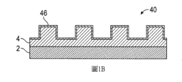
2‧‧‧基材 2‧‧‧Substrate
4‧‧‧圖案化層 4‧‧‧Patterned layer
6‧‧‧液體溶液 6‧‧‧Liquid solution
7‧‧‧轉移層/圖案化層 7‧‧‧Transfer layer/Patterned layer
8‧‧‧金屬層 8‧‧‧Metal layer
8’‧‧‧金屬層 8’‧‧‧Metal layer
40‧‧‧圖案化表面 40‧‧‧Patterned surface
42‧‧‧凹入特徵 42‧‧‧Concave features
44‧‧‧高原特徵 44‧‧‧Plateau Characteristics
44’‧‧‧高原特徵 44’‧‧‧Plateau Characteristics
46‧‧‧離型塗層 46‧‧‧Release coating
52‧‧‧網格 52‧‧‧grid
54‧‧‧圖案化構造/開放面積 54‧‧‧Patterned structure/open area
54’‧‧‧圖案化構造 54’‧‧‧Patterned construction
61‧‧‧表面位準 61‧‧‧Surface level
62‧‧‧可釋離固體層/固體層 62‧‧‧Releasable solid layer/solid layer
62’‧‧‧固體層 62’‧‧‧Solid layer
64‧‧‧固化產物殘餘物/殘餘物 64‧‧‧Cure product residue/residue
66‧‧‧步驟 66‧‧‧Steps
72‧‧‧背襯層/背襯 72‧‧‧Backing layer/backing
74‧‧‧黏著劑層 74‧‧‧Adhesive layer
82‧‧‧第一部分/金屬層 82‧‧‧Part 1/Metal Layer
82’‧‧‧第一部分/金屬層 82’‧‧‧Part 1/Metal Layer
84‧‧‧第二部分/剩餘金屬層/金屬圖案 84‧‧‧
84’‧‧‧第二部分/金屬圖案 84’‧‧‧
92‧‧‧第一部分/金屬層 92‧‧‧Part 1/Metal Layer
92’‧‧‧第一部分/金屬層 92’‧‧‧Part 1/Metal Layer
94‧‧‧第二部分/金屬層/金屬圖案 94‧‧‧
94’‧‧‧第二部分/金屬圖案 94’‧‧‧
522‧‧‧突起特徵 522‧‧‧Protruding features
542‧‧‧突起特徵 542‧‧‧Protruding features
544‧‧‧凹部 544‧‧‧Concave
544’‧‧‧凹部 544’‧‧‧Concave
配合附圖,思考如下所述本揭露各個實施例之實施方式,可更完整地理解本揭露,其中: The present disclosure can be more completely understood by considering the implementation of various embodiments of the present disclosure as follows with reference to the accompanying drawings, wherein:
圖1A係根據一個實施例之具有圖案化表面之可撓性基材之剖面圖。 Figure 1A is a cross-sectional view of a flexible substrate with a patterned surface, according to one embodiment.
圖1B繪示根據一個實施例之處理圖1A之圖案化表面以形成離型塗層於圖案化表面上的程序。 FIG. 1B illustrates a process of treating the patterned surface of FIG. 1A to form a release coating on the patterned surface according to one embodiment.
圖1C繪示根據一個實施例之將液體溶液塗佈至圖1B的圖案化表面上的程序。 Figure 1C illustrates a process for applying a liquid solution onto the patterned surface of Figure IB, according to one embodiment.
圖1D繪示根據一個實施例之乾燥圖1C之液體溶液以形成固體層之方法。 Figure 1D illustrates a method of drying the liquid solution of Figure 1C to form a solid layer, according to one embodiment.
圖2A繪示根據一個實施例之提供金屬層至圖1D之圖案化表面上的程序。 Figure 2A illustrates a process of providing a metal layer onto the patterned surface of Figure ID, according to one embodiment.
圖2B繪示根據一個實施例之移除圖2A之固體層連同該固體層上的金屬層之程序。 FIG. 2B illustrates a process of removing the solid layer of FIG. 2A together with the metal layer on the solid layer according to one embodiment.
圖3A繪示根據一個實施例之蝕刻圖1D之圖案化表面之程序。 Figure 3A illustrates a process for etching the patterned surface of Figure ID, according to one embodiment.
圖3B繪示根據一個實施例之提供金屬層至圖3A之圖案化表面上的程序。 Figure 3B illustrates a process of providing a metal layer onto the patterned surface of Figure 3A, according to one embodiment.
圖3C繪示根據一個實施例之移除圖3B之固體層連同該固體層上的金屬層之程序。 FIG. 3C illustrates a process of removing the solid layer of FIG. 3B together with the metal layer on the solid layer according to one embodiment.
圖4A繪示根據一個實施例之提供轉移層至圖1D之圖案化表面上的程序。 Figure 4A illustrates a process for providing a transfer layer onto the patterned surface of Figure ID, according to one embodiment.
圖4B繪示根據一個實施例之從圖案化表面移除圖4A的轉移層連同固體層之後以於其上形成圖案化構造的該轉移層的剖面圖。 4B illustrates a cross-sectional view of the transfer layer of FIG. 4A after removing the transfer layer along with the solid layer from a patterned surface to form a patterned structure thereon, according to one embodiment.
圖5A繪示根據一個實施例之在圖4B的圖案化構造上提供金屬層之程序。 Figure 5A illustrates a process of providing a metal layer on the patterned structure of Figure 4B, according to one embodiment.
圖5B繪示根據一個實施例之從圖5A的圖案化構造移除固體層連同該固體層上的金屬層之程序。 Figure 5B illustrates a process of removing a solid layer together with a metal layer on the solid layer from the patterned structure of Figure 5A, according to one embodiment.
圖6A繪示根據一個實施例之蝕刻圖4B之圖案化表面之程序。 Figure 6A illustrates a process for etching the patterned surface of Figure 4B, according to one embodiment.
圖6B繪示根據一個實施例之提供金屬層至圖6A之圖案化表面上的程序。 Figure 6B illustrates a process of providing a metal layer onto the patterned surface of Figure 6A, according to one embodiment.
圖6C繪示根據一個實施例之移除圖6B之固體層連同該固體層上的金屬層之程序。 FIG. 6C illustrates a process of removing the solid layer of FIG. 6B together with the metal layer on the solid layer according to one embodiment.
圖7係根據一個實施例之基材上之金屬圖案的示意圖之俯視平面圖。 Figure 7 is a top plan view of a schematic diagram of a metal pattern on a substrate according to one embodiment.
圖8繪示實例8之顯微影像。 Figure 8 shows a microscopic image of Example 8.
圖9繪示實例9之顯微影像。 Figure 9 shows a microscopic image of Example 9.
圖式中,相似元件符號指代相似元件。雖然上述所提出之圖式闡述本揭露之數個實施例,其他在實施方式中所提到的實施例亦被考慮,該等圖式可未按比例繪製。在所有情況中,本揭露係藉由例示性實施例的表示之方式而非明確的限制來說明所揭示之揭露。應理解,所屬技術領域中具有通常知識者可擬定出許多其他修改及實施例,其仍屬於本揭露之範疇及精神。 In the drawings, similar component symbols refer to similar components. Although the above-described drawings illustrate several embodiments of the present disclosure, other embodiments are also contemplated and the drawings may not be drawn to scale. In all cases, the disclosure is presented by way of representation of illustrative embodiments and not by express limitation. It is understood that many other modifications and embodiments can be devised by those of ordinary skill in the art, which still fall within the scope and spirit of the present disclosure.
對於下文所定義用語的詞彙,這些定義應適用於整份申請書,除非在申請專利範圍或說明書中的別處提供不同定義。 For terms defined below, these definitions shall apply to the entire application unless a different definition is provided elsewhere in the claim or specification.
說明書及申請專利範圍中使用某些用語,雖然這些用語大多數已為人所熟知,但可能需要一些解釋。應理解: Certain terms are used in the description and patent claims, and although most of these terms are well known, they may require some explanation. It should be understood:
針對所揭示之塗佈物品中之各種元件的位置使用定向用語,諸如「在...頂部上(atop)」、「在...上(on)」、「在...上方(over)」、「覆蓋(covering)」、「最上(uppermost)」、「下伏(underlying)」、及類似用語時,係指元件相對於水平設置、面向上基材之相對位置。然而,除非另有說明,否則基材或物品在製造期間或之後應具有任何特定空間定向非係所意欲的。 Use of directional terms such as "atop," "on," and "over" with respect to the location of various elements in the disclosed coated articles ”, “covering”, “uppermost”, “underlying”, and similar terms refer to the relative position of the component relative to a horizontally arranged, upward-facing substrate. However, it is not intended that the substrate or article should have any specific spatial orientation during or after manufacture, unless otherwise stated.
為描述本揭露之物品之一層相對於一基材或另一元件的位置而使用用語「披覆(overcoated)」,係指該層在該基材或另一元件之頂上,但不必接近於該基材或該另一元件。 The term "overcoated" is used to describe the position of a layer of an article of the present disclosure relative to a substrate or another element, meaning that the layer is on top of, but not necessarily proximate to, the substrate or other element. the substrate or the other element.
為描述一層相對於其他層的位置而使用用語「由...分開(separated by)」,係指該層係定位於兩個其他層之間,但不必接近於或相鄰於任一層。 The use of the term "separated by" to describe the position of a layer relative to other layers means that the layer is positioned between two other layers but is not necessarily close to or adjacent to either layer.
關於數值或形狀的用語「約(about)」或「近似(approximately)」係意指該數值或性質或特性的+/-五百分比,但明確地包括該確切數值。例如,「約」1Pa-sec之黏度係指自0.95至1.05Pa-sec之黏度,而且亦明確地包含確切1Pa-sec之黏度。同樣地,「實質上正方形」周長意欲描述具有四個側向邊緣之幾何形狀,其中各側向邊緣之長度為任何其他側向邊緣之長度的自95%至105%,而且亦包含各側向邊緣具有完全相同長度的幾何形狀。 The terms "about" or "approximately" with respect to a numerical value or shape mean +/- five percent of that numerical value or property or characteristic, but expressly include the exact numerical value. For example, a viscosity of "about" 1 Pa-sec refers to a viscosity from 0.95 to 1.05 Pa-sec, and specifically includes a viscosity of exactly 1 Pa-sec. Likewise, a "substantially square" perimeter is intended to describe a geometric shape with four lateral edges, where the length of each lateral edge is from 95% to 105% of the length of any other lateral edge, and also includes Geometry with exactly the same length toward the edge.
關於屬性或特性的用詞「實質上(substantially)」意指該屬性或特性的展現程度大於該屬性或特性之相對者的展現程度。例如,「實質上」透明之基材係指所透射的輻射(例如,可見光)多於未能透射者(例如,吸收及反射)之基材。因此,透射入射在其表面上之多於50%可見光的基材係實質上透明,而透射入射在其表面上之50%或更少可見光的基材係非實質上透明。 The word "substantially" with respect to an attribute or characteristic means that the attribute or characteristic is exhibited to a greater extent than its counterpart. For example, a "substantially" transparent substrate is one that transmits more radiation (eg, visible light) than does not transmit (eg, absorbs and reflects). Thus, a substrate that transmits more than 50% of visible light incident on its surface is substantially transparent, while a substrate that transmits 50% or less of visible light incident on its surface is not substantially transparent.
如本說明書及隨附實施例中所用者,單數形式「一(a/an)」及「該(the)」包括複數的指涉,除非內容另有清楚指定。因此,例如,對於含有「一化合物」之細纖維之參照包含二或更多種化合物 之混合物。如本說明書及所附實施例中所使用者,用語「或(or)」通常是用來包括「及/或(and/or)」的意思,除非內文明確地另有指示。 As used in this specification and the accompanying examples, the singular forms "a/an" and "the" include plural referents unless the content clearly dictates otherwise. Thus, for example, a reference to fine fibers containing "a compound" includes a mixture of two or more compounds. As used in this specification and the accompanying examples, the term "or" is generally intended to include "and/or" unless the context clearly dictates otherwise.
如本說明書中所使用,以端點敘述之數字範圍包括所有歸於該範圍內的數字(例如,1至5包含1、1.5、2、2.75、3、3.8、4及5)。 As used in this specification, numerical ranges recited by endpoints include all numbers falling within that range (eg, 1 to 5 includes 1, 1.5, 2, 2.75, 3, 3.8, 4, and 5).
除非另有所指,否則本說明書及實施例中所有表達量或成分的所有數字、屬性之測量及等等,在所有情形中都應予以理解成以用語「約(about)」進行修飾。因此,除非另有相反指示,否則在前述說明書及隨附實施例清單所提出的數值參數,可依據所屬技術領域中具有通常知識者運用本揭露的教示而企圖獲得之所欲性質而有所變化。起碼,至少應鑑於有效位數的個數,並且藉由套用普通捨入技術,詮釋各數值參數,但意圖不在於限制所主張實施例範疇均等論之應用。 Unless otherwise indicated, all numbers expressing quantities or ingredients, measurements of properties, and the like in this specification and the examples should be understood in all cases to be modified by the word "about." Accordingly, unless otherwise indicated to the contrary, the numerical parameters set forth in the foregoing specification and accompanying list of examples may vary depending on the desired properties that one of ordinary skill in the art attempts to obtain by applying the teachings of the present disclosure. . At a minimum, each numerical parameter should be interpreted in light of the number of significant digits and by applying ordinary rounding techniques, but it is not intended to limit the application of the categorical egalitarianism of the claimed embodiments.
現將特別參照該等圖式說明本揭露的各個例示性實施例。本揭露之例示性實施例可有各種修改及改變,而不悖離本揭露之精神及範疇。因此,應理解本揭露之該等實施例不受限於以下所述的例示性實施例,而是由該等申請專利範圍及任何其均等者所提限制所管制。 Various exemplary embodiments of the present disclosure will now be described with particular reference to the drawings. Various modifications and changes may be made to the exemplary embodiments of the disclosure without departing from the spirit and scope of the disclosure. Therefore, it should be understood that the embodiments of the present disclosure are not limited to the illustrative embodiments described below, but are governed by the limitations set forth in the patent scope of these claims and any equivalents thereof.
圖1A係根據一個實施例之具有圖案化表面之可撓性基材之剖面圖。圖案化表面40係形成在可撓性基材2的主表面上。圖案化表面40包括一或多個凹入特徵42及相鄰於該等凹入特徵42之一或多個高原特徵44。在一些實施例中,高原特徵44可形成網格構形,諸如在圖7中所示之網格52。本文所述之網格一般係理解為意指圖案幾何,其具有藉由開放面積54分開以形成單元(cell)的連接跡線。具有線 性跡線之網格的說明性實例包括例如具有六邊形及正方形單元者。在一些實施例中,網格的開放面積可例如大於90%、大於95%、或大於98%。高原特徵44可具有在例如約50nm至約5微米、或約100nm至約3微米之範圍中的平均線寬;以及在例如約50nm至約5微米、或約100nm至約3微米之範圍中之平均高度。 Figure 1A is a cross-sectional view of a flexible substrate with a patterned surface, according to one embodiment. The patterned
在一些實施例中,基材2可係可撓性基材,例如,不定長度聚合材料的帶材。可撓性基材或帶材在沿著帶材路徑移動時可被(例如,沿著機器方向及/或橫向)拉伸。該可撓性基材可包括,例如,聚對苯二甲酸乙二酯(polyethylene terephthalate,PET)、聚乙烯、聚苯乙烯、聚胺甲酸酯等。本文描述的程序可在包括一或多個輥以沿著帶材路徑輸送帶材的一卷對卷設備上進行。基材2可具有例如約2mm或更小、約1mm或更小、約500微米或更小,或約200微米或更小的厚度。 In some embodiments,
在一些實施例中,圖案化表面40可直接形成於可撓性基材2上。在圖1A所描繪的實施例中,圖案化表面40係形成在圖案化層4上,該圖案化層係設置於基材2上。 In some embodiments, patterned
在一些實施例中,圖案化表面40可藉由一微複製程序形成於基材2上。在一些實施例中,可將可固化材料層提供於基材2上以形成圖案化層4。該可固化材料可包括例如聚二甲基矽氧烷(polydimethylsiloxane,PDMS)、環氧樹脂、UV可固化丙烯酸酯樹脂等。可提供微複製印模以壓靠可固化材料層以於其上建立複製特徵。可固化材料可使用各種方法固化,該等方法包括,例如熱、UV、電子 束輻射等。應瞭解,圖案化表面40可藉由任何合適的方法形成於基材2上,諸如,例如壓紋、微模製、微匹配、雷射蝕刻、3D列印等。 In some embodiments, the patterned
在一些實施例中,圖案化層4可包括一或多種展現相對低表面黏著強度的離型塗層材料。此類離型塗層材料可包括例如矽氧烷、聚矽氧、聚四氟乙烯等。 In some embodiments, patterned
在一些實施例中,圖案化表面40可經處理以降低其表面黏著強度。在圖1B所描繪的實施例中,根據一個實施例處理圖1A之圖案化表面40以在該圖案化表面上形成離型塗層46。在一些實施例中,離型塗層46可藉由電漿沉積程序來形成。可將氣體六甲基二矽氧烷(hexamethyldisiloxane,HMDSO)引入反應腔室中,並在電漿存在下,以在圖案化表面40上形成離型塗層。離型塗層可具有例如小於約500nm、小於約200nm、或小於100nm之厚度。例示性電漿沉積程序及設備係描述於WO 2018/005109(Yu等人)中,該案以引用方式併入本文中。 In some embodiments, patterned
可將液體溶液提供至圖案化表面40上,以在該圖案化表面上選擇性地形成可釋離固體層。在圖1C的實施例中,在形成離型塗層46之後,將液體溶液6提供至圖案化表面40上。液體溶液6填充凹入特徵42中且覆蓋高原特徵44。在圖1C之所描繪的實施例中,液體溶液6具有高於高原特徵44之表面位準61。應瞭解,在一些實施例中,液體溶液6可具有低於高原特徵44之表面位準61且僅存在於凹入特徵42中。 A liquid solution can be provided onto the patterned
在一些實施例中,液體溶液6可為聚(乙烯醇)(PVA)於水中之溶液。應理解,液體溶液可包括其他溶質,諸如例如聚乙烯丁醛(polyvinyl butyral,PVB)、可固化丙烯酸酯、膜形成劑(film former)等。液體溶液可溶解於任何常見溶劑組合中,諸如水、異丙醇、甲基乙基酮、己烷、乙酸乙酯。液體組成物之表面能可藉由添加界面活性劑來修改,諸如,例如聚乙二醇p-(1,1,3,3-四甲基丁基)-苯基醚(可以商標名稱TritonTM X-100購自Sigma-Aldrich Chemical company,Milwaukee,WI)。 In some embodiments, the liquid solution 6 may be a solution of poly(vinyl alcohol) (PVA) in water. It is understood that the liquid solution may include other solutes such as, for example, polyvinyl butyral (PVB), curable acrylates, film formers, and the like. Liquid solutions are soluble in any common solvent combination such as water, isopropyl alcohol, methyl ethyl ketone, hexane, ethyl acetate. The surface energy of liquid compositions can be modified by adding surfactants such as, for example, polyethylene glycol p-(1,1,3,3-tetramethylbutyl)-phenyl ether (available under the trade name Triton ™ X-100 was purchased from Sigma-Aldrich Chemical company, Milwaukee, WI).
然後將液體溶液6固化以在凹入特徵42中形成可釋離固體層62。在一些實施例中,液體溶液6可藉由在例如約25℃至約175℃、或約50℃至約100℃的溫度下乾燥來固化。圖案化表面40具有相對低表面黏著強度,使得固體層62可例如藉由剝離或清洗而與凹入特徵42分離或釋離。在圖1D之所描繪的實施例中,在該固化之後,固化產物殘餘物64留在高原特徵44上。固化產物殘餘物64具有較凹入特徵中固體層62之乾燥厚度更薄的乾燥厚度。在一些實施例中,固化產物殘餘物64可具有例如凹入特徵中固體層62之乾燥厚度之約½或更小、約1/3或更小、約1/5或更小、或約1/10或更小之乾燥厚度。 Liquid solution 6 is then solidified to form releasable
在所描繪的實施例中,高原特徵44各具有平坦頂部表面。在一些實施例中,高原特徵44可具有各種突起形狀,諸如,例如稜柱或角錐形狀、半球形形狀、似子彈(bullet-like)的形狀等。各種突起特徵係描述於美國專利第8,703,232(Stay等人)中,該案以引用方式併入本文中。在一些實施例中,高原特徵44可具有允許液體溶液6 從該等高原特徵流至凹入特徵42中之突起形狀以減少在高原特徵44上之固化產物殘餘物64的量。在一些實施例中,高原特徵44可具有疏水性表面特性,該等疏水性表面特性排斥液體溶液6以從高原特徵流至凹入特徵中。 In the depicted embodiment, the plateau features 44 each have a flat top surface. In some embodiments, plateau features 44 may have various protruding shapes, such as, for example, prism or pyramid shapes, hemispherical shapes, bullet-like shapes, and the like. Various raised features are described in U.S. Patent No. 8,703,232 (Stay et al.), which is incorporated herein by reference. In some embodiments, the plateau features 44 may have a protruding shape that allows liquid solution 6 to flow from the plateau features into the recessed features 42 to reduce the amount of solidified
在形成可釋離固體層62於凹入特徵中之後,可將導電層提供至圖案化表面上。該導電層可為例如金屬層,或包括任何適合的導電材料。圖2A繪示根據一個實施例之提供金屬層8以覆蓋圖1D的圖案化表面。金屬層8之第一部分82係設置在凹入特徵42中;且金屬層8之第二部分84設置在高原特徵44之頂部表面上。 After forming the releasable
金屬層8可藉由任何所欲程序形成,包括例如蒸鍍、濺鍍、電子束沉積、物理氣相沉積、化學氣相沉積、液體塗佈等。在一些實施例中,該金屬層可包括多個層,例如,包括直接接觸至該圖案化表面之連結層(tie-layer)、及該連結層頂部上之另一金屬(例如,銅、銀、金、鋁等)之層。連結層(亦已知為膠或助黏層)可包括鉻、鉻氧化物、ITO、AZO、鎳、鈦等。應理解,該金屬層可包括任何適合的導電材料。 The
在一些實施例中,金屬層8可具有例如約0.01微米至約2微米、約0.02微米至約1微米、或約0.025微米至約0.5微米的平均厚度。在一些實施例中,金屬層8可為連續的、具有與圖案化表面之表面形態適形的一或多個表面,且具有大致均勻的厚度。在一些實施例中,金屬層8可具有非均勻厚度。例如,如在圖2A中所繪示,在步驟66的金屬層8可具有減小的厚度或甚至是中斷的。 In some embodiments,
在形成金屬層於圖案化表面上之後,可執行起離程序以從該圖案化表面移除在該等凹入特徵中之可釋離固體層62連同該可釋離固體層上之金屬層82。圖案化表面40上的剩餘金屬層84形成金屬圖案,如圖2B所示。 After the metal layer is formed on the patterned surface, a lift-off process can be performed to remove the releasable
在一些實施例中,固體層62可為水溶性聚合物層,其可藉由例如壓力清洗、超音波清洗等而從圖案化表面40移除。當固體層62包括聚(乙烯醇)(PVA)時,可藉由水清洗將固體層62溶解並從基材釋離。在一些實施例中,固體層62可藉由剝離來移除。在一個實施例中,可將可固化樹脂層(例如丙烯酸酯樹脂)澆鑄在圖案化表面40上。可固化該可固化樹脂層且可從該圖案化表面40剝離該可固化樹脂層連同在該等凹入特徵中之金屬層與可釋離固體層。可固化樹脂材料可對金屬層具有合適親和力,使得在高原頂部的金屬層可留在圖案化表面上,而可移除可釋離固體層連同該可釋離固體層上的金屬層。在一些實施例中,金屬層可以使得其更強力地黏附至圖案化表面之方式施加,諸如,例如使用濺鍍及/或使用連結層來沉積。 In some embodiments,
應理解,可釋離固體層62可係任何適當的抗蝕層,其可藉由施加例如溶劑、熱、冷卻、剝離等而從圖案化表面40移除。在一些實施例中,凹入特徵中的固體層62下方的離型塗層46可連同固體層62完全或部分移除。 It is understood that releasable
在一些實施例中,固化後留在高原特徵44上之固化產物殘餘物64(例如參見圖1D)可在提供金屬層在高原特徵上之前移除。在圖3A之所描繪的實施例中,藉由蝕刻將殘餘物64從高原特徵44’移 除。可使用任何合適的蝕刻程序,包括例如反應性離子蝕刻(RIE),諸如氧或八氟丙烷電漿蝕刻。在從高原特徵44移除固化產物殘餘物64之後,蝕刻程序可繼續移除下方離型塗層46(參見圖1B)以曝露出高原特徵44之頂部表面。在一些實施例中,該RIE可移除固化產物殘餘物,且接著修改下方離型塗層46之化學性質。蝕刻亦可稍微減少固體層62’在凹入特徵中的厚度。在一些實施例中,固體層62’的厚度可減少達例如小於20%、小於10%、或小於5%。 In some embodiments, cured product residue 64 (see, eg, FIG. ID) remaining on plateau features 44 after curing may be removed prior to providing a metal layer over the plateau features. In the embodiment depicted in Figure 3A,
本文中所用之蝕刻程序可用來修改離型塗層46(在高原特徵上)之化學性質。此類修改可有利於改善設置於離型塗層上之金屬層的黏著性。本文中所使用的蝕刻程序可被良好控制,使得其不會導致在可釋離固體層中之交聯,該交聯可導致固體層更強力地黏附至基材,且較不可溶於水。在本文中所述的程序相較傳統的熱印痕微影程序係技術上有利的,諸如在美國專利第5,772,905號(CHou等人)中所述者,其中重反應性離子蝕刻程序可劣化基材表面及其後形成的金屬/基材介面。 The etching procedures used herein can be used to modify the chemistry of the release coating 46 (over the plateau features). Such modifications can help improve the adhesion of the metal layer disposed on the release coating. The etching procedure used herein can be well controlled such that it does not result in cross-linking in the releasable solid layer, which may cause the solid layer to adhere more strongly to the substrate and be less soluble in water. The procedures described herein are technically advantageous over traditional thermal imprint lithography procedures, such as those described in U.S. Patent No. 5,772,905 (Chou et al.), where heavy reactive ion etching procedures can degrade the substrate The surface and subsequent metal/substrate interface.
蝕刻後,可將導電層提供至該圖案化表面上。圖3B繪示根據一個實施例之提供金屬層8’以覆蓋圖3A之圖案化表面的程序。該金屬層8’之第一部分82’係設置在該等凹入特徵中之可釋離固體層62’上;且該金屬層8’之第二部分84’係直接設置在高原特徵44’之頂部表面上。可執行起離程序以移除凹入特徵中的固體層62’連同其上的金屬層82’。圖3C係在高原特徵44’上之金屬圖案84’的剖面圖。 After etching, a conductive layer can be provided onto the patterned surface. Figure 3B illustrates a process of providing a metal layer 8' to cover the patterned surface of Figure 3A, according to one embodiment. The first portion 82' of the metal layer 8' is disposed on the releasable solid layer 62' in the recessed features; and the second portion 84' of the metal layer 8' is disposed directly on the
在一些實施例中,可使用以選擇性形成之可釋離固體層覆蓋之圖案化表面(諸如在圖1D中所示的結構)作為製造金屬化圖案的模製表面。應瞭解,該圖案化表面可由其他適合的材料製造,例如金屬。圖4A繪示根據一個實施例之提供轉移層至圖1D之圖案化表面上的程序。在一些實施例中,固化後留在高原特徵44上之固化產物殘餘物64(例如參見圖1D)可在提供轉移層在高原特徵上之前移除,諸如描繪於圖3A中的實施例。 In some embodiments, a patterned surface covered with a selectively formed releasable solid layer, such as the structure shown in Figure ID, can be used as the molding surface to create the metallization pattern. It will be appreciated that the patterned surface may be fabricated from other suitable materials, such as metal. Figure 4A illustrates a process for providing a transfer layer onto the patterned surface of Figure ID, according to one embodiment. In some embodiments, cured product residue 64 (eg, see FIG. 1D) remaining on plateau features 44 after curing may be removed prior to providing a transfer layer over the plateau features, such as the embodiment depicted in FIG. 3A.
轉移層7包括直接接觸圖案化層4之圖案化表面的黏著劑層74。黏著劑層74係由可撓性背襯層72支撐。在一些實施例中,黏著劑層74可藉由提供可固化液體至圖案化表面上以形成固化產物而形成。在一些實施例中,黏著劑層可藉由以下而至少部分地形成:使可釋離固體層62再溶解,並且使用該再溶解層作為該黏著劑層之至少一部分。黏著劑層亦可溶劑塗佈至背襯72上或在圖案化表面的頂部上。 The
黏著劑層74可包括具有所欲性質之任何合適黏著劑材料。黏著劑層74可為可剝離或可拉伸釋離且可從基材2之圖案化表面剝離。在一些實施例中,黏著劑可包括橡膠、聚矽氧、或基於丙烯酸之黏著劑中之至少一者。在一些實施例中,黏著劑可包括膠黏橡膠黏著劑,諸如天然橡膠;烯烴;聚矽氧,例如聚矽氧聚脲或聚矽氧嵌段共聚物;合成橡膠黏著劑,例如聚異戊二烯、聚丁二烯、及苯乙烯-異戊二烯-苯乙烯、苯乙烯-乙烯-丁烯-苯乙烯以及苯乙烯-丁二烯-苯乙烯嵌段共聚物、以及其它合成彈性體;以及膠黏或未膠黏丙烯酸黏著劑,例如丙烯酸異辛酯與丙烯酸之共聚物,其係可藉由輻射、溶解、懸浮、 或乳化技術而被聚合;聚胺甲酸酯;聚矽氧嵌段共聚物;以及上述之組合。該黏著劑可為例如下列專利申請案之任何者中所述之黏著劑的任何者,其等全部係以引用方式併入本文中:PCT專利公開案第2015/035556號、第2015/035960號、及美國專利公開案第2015/034104號。
在一些實施例中,背襯層72可具有足夠的可撓性,使得轉移層7可提供適形性與彈性性質,該等性質在黏著劑層74黏附至圖案化層7的圖案化表面時、且在藉由剝離來將該黏著劑層自其移除時是有幫助的。在一些實施例中,可撓性背襯層72可包括可撓性聚合膜。該可撓性背襯層72可包括,例如聚對苯二甲酸乙二酯(PET)、聚乙烯、聚苯乙烯、聚胺甲酸酯等。本文描述的程序可在包括一或多個輥以沿著帶材路徑輸送帶材的一卷對卷設備上進行。轉移層7可具有例如約2mm或更小、約1mm或更小、約500微米或更小,或約200微米或更小的厚度。 In some embodiments, the
當轉移層7從基材2剝離時,可釋離固體層62及(在一些實施例中)固化產物殘餘物64可附接至黏著劑層74並從圖案化層4轉移至轉移層7。圖4B繪示形成圖案化構造54之轉移層7的剖面圖。在所描繪的實施例中,圖案化構造54可為圖1A之圖案化表面40的負浮雕。圖案化構造54包括對應於圖1A之圖案化表面40之凹入特徵42的突起特徵542、及對應於圖1A之高原特徵44的凹部544。突起特徵542具有包括可釋離固體層62之頂部部分、及包括黏著劑層74之材料的底部部分。固化產物殘餘物64附接至凹部544之底部表面。應瞭解, 離型塗層46(參見圖1B)可至少部分地沿著固體層62及固化產物殘餘物64自圖案化層4轉移至轉移層7,該轉移層分別覆蓋固體層62及固化產物殘餘物64。 When
在一些實施例中,凹部544可形成網格構形,諸如在圖7中所示之網格52。本文所述之網格一般係理解為意指圖案幾何,其具有藉由開放面積分開以形成單元的連接跡線。具有線性跡線之網格的說明性實例包括例如具有六邊形及正方形單元者。凹部544可具有在例如約50nm至約5微米之範圍中之平均線寬、及在例如約50nm至約5微米之範圍中之平均深度。 In some embodiments, recesses 544 may form a grid configuration, such as
可將金屬層提供至該轉移層之圖案化構造上。圖5A繪示根據一實施例之在圖4B之圖案化構造54上的金屬層之剖面圖。該金屬層包括設置在突起特徵542之頂部表面上的第一部分92、以及設置在該等凹部544之底部表面上的第二部分94。 A metal layer can be provided onto the patterned structure of the transfer layer. Figure 5A illustrates a cross-sectional view of a metal layer on the patterned
該金屬層可藉由任何所欲程序形成,包括例如蒸鍍、濺鍍、電子束沉積、物理氣相沉積、化學氣相沉積、液體塗佈等。在一些實施例中,該金屬層可包括多個層,例如,包括直接接觸至該圖案化表面之連結層(例如,鎳或鈦)、及該連結層頂部之另一金屬(例如,銅、銀、金、鋁等)之層。 The metal layer can be formed by any desired process, including, for example, evaporation, sputtering, electron beam deposition, physical vapor deposition, chemical vapor deposition, liquid coating, etc. In some embodiments, the metal layer may include multiple layers, including, for example, a tie layer (eg, nickel or titanium) in direct contact with the patterned surface, and another metal (eg, copper, titanium, etc.) on top of the tie layer. Silver, gold, aluminum, etc.) layer.
如在圖5A中所繪示,金屬層之第一部分92及第二部分94彼此分開。亦即,金屬層未適形地形成於突起特徵542之側上。應理解,該金屬層可至少部分地以減小厚度形成在突起特徵542之側上。 As shown in Figure 5A, the
在一些實施例中,凹部544中之金屬層94可具有例如約0.01微米至約2微米、約0.02微米至約1微米、或約0.025微米至約0.5微米之平均厚度。在一些實施例中,凹部544中之金屬層94可係連續的、具有與凹部544之底部表面之表面形態適形的一或多個表面、且具有一大致上均勻的厚度。在一些實施例中,金屬層94可具有非均勻厚度。 In some embodiments,
在形成金屬層於轉移層7上之後,可執行起離程序以移除突起特徵542上之固體層62連同該固體層上的金屬層92。在一些實施例中,固體層62可為水溶性聚合物層,其可藉由例如壓力清洗從轉移層7移除。當固體層62包括聚(乙烯醇)(PVA)時,可藉由水清洗將固體層62溶解且自基材釋離。在一些實施例中,固體層62可藉由剝離來移除。在一個實施例中,可將可固化樹脂層澆鑄在轉移層7上。可固化該可固化樹脂層且可從該圖案化構造54剝離該可固化樹脂層連同在該等突起特徵上之金屬層與固體層。圖5B係凹部544中之剩餘金屬圖案94的剖面圖。 After the metal layer is formed on the
在一些實施例中,留在該轉移層7之凹部544中的固化產物殘餘物64(見例如圖4B)可在提供金屬層至轉移層7上之前移除。在圖6A中所描繪之實施例中,藉由蝕刻從凹部544之底部表面移除固化產物殘餘物64。可使用任何合適的蝕刻程序,包括例如反應性離子蝕刻(RIE),諸如氧或八氟丙烷電漿蝕刻。 In some embodiments, cured
在一些實施例中,蝕刻可先移除表面上的離型塗層46(若適用),並繼續移除下方的固化產物殘餘物64以曝露出凹部544 之底部表面。該蝕刻亦可稍微減少突起特徵522之固體層62的厚度。在一些實施例中,固體層62的厚度可減少達例如小於20%、小於10%、或小於5%。 In some embodiments, the etching may first remove the
在蝕刻之後,可將金屬層提供至圖6A之圖案化構造54’上。圖6B繪示根據一個實施例之提供金屬層以覆蓋圖6A之圖案化構造54’之程序。該金屬層之第一部分92’係設置在突起特徵之固體層62上;且該金屬層之第二部分94’直接設置在凹部544’之底部表面上。可執行起離程序以從轉移層7移除固體層62’連同其上的金屬層92’。圖6C為在轉移層7之凹部544’中的金屬圖案94’之剖面圖。 After etching, a metal layer may be provided over the patterned structure 54' of Figure 6A. Figure 6B illustrates a process of providing a metal layer to cover the patterned structure 54' of Figure 6A, according to one embodiment. The first portion 92' of the metal layer is disposed on the
可將本文所述之金屬圖案(例如在圖2B中的84、在圖3C中的84’、在圖5B中的94、在圖6C中的94’)應用於各種裝置。在一些實施例中,該等金屬圖案可僅設置在圖案化表面的高原特徵上,以在可撓性基材上形成網格形狀。在一些實施例中,該等金屬圖案可僅設置在圖案化表面的凹部中,以在可撓性基材上形成網格形狀。金屬圖案可具有例如約20nm至500nm的厚度。在一些實施例中,具有支撐金屬圖案之圖案化表面的可撓基材可係透明的。在一些實施例中,具有金屬圖案之圖案化表面可以與結構化層之頂部層折射率匹配的材料回填。例示性回填材料描述於美國專利第8703232號(Stay等人)中,該案以引用方式併入本文。 The metal patterns described herein (e.g., 84 in Figure 2B, 84' in Figure 3C, 94 in Figure 5B, 94' in Figure 6C) can be applied to a variety of devices. In some embodiments, the metal patterns may be disposed only on plateau features on the patterned surface to form a grid shape on the flexible substrate. In some embodiments, the metal patterns may be disposed only in the recesses of the patterned surface to form a grid shape on the flexible substrate. The metal pattern may have a thickness of about 20 nm to 500 nm, for example. In some embodiments, a flexible substrate having a patterned surface supporting a metal pattern can be transparent. In some embodiments, the patterned surface with the metal pattern can be backfilled with a material that matches the refractive index of the top layer of the structured layer. Exemplary backfill materials are described in U.S. Patent No. 8,703,232 (Stay et al.), which is incorporated herein by reference.
雖然上述說明提供在可撓性基材上的金屬或其他導電材料的網格圖案,但是應理解,可依類似方式在該可撓性基材上形成其他材料的圖案。例如,用於此一圖案的材料可包括陶瓷、墨水、或任 何合適的光學材料。此外,類似程序/方法可用以製造在可撓基材上的網格以外的合適圖案。 Although the above description provides a grid pattern of metal or other conductive material on a flexible substrate, it should be understood that patterns of other materials can be formed on the flexible substrate in a similar manner. For example, materials used for this pattern may include ceramics, ink, or any suitable optical material. Additionally, similar procedures/methods can be used to create suitable patterns other than grids on flexible substrates.
可依連續或卷對卷方式執行本文所述之程序,諸如,例如,微複製、電漿塗佈、蝕刻、塗佈、固化/乾燥、層壓、剝離、金屬沉積(例如,濺鍍)、金屬蒸鍍等。例示性連續或卷對卷的微複製程序係描述於美國專利第9759663號(Halverson等人)中。例示性電漿塗佈及蝕刻之連續或卷對卷程序係描述於美國專利第8460568號(David等人)中。例示性塗佈及乾燥之連續或卷對卷程序係描述於美國專利第8623140號(Yapel等人)中。在塗佈步驟後可添加帶材的層壓及剝除。例示性金屬沉積的連續或卷對卷程序係描述於美國專利第6172810號(Fleming等人)中。 The processes described herein may be performed in a continuous or roll-to-roll manner, such as, for example, microreplication, plasma coating, etching, coating, curing/drying, lamination, lift-off, metal deposition (e.g., sputtering), Metal evaporation, etc. Exemplary continuous or roll-to-roll microreplication procedures are described in US Patent No. 9,759,663 (Halverson et al.). Exemplary continuous or roll-to-roll processes for plasma coating and etching are described in US Patent No. 8,460,568 (David et al.). Exemplary continuous or roll-to-roll procedures for coating and drying are described in US Patent No. 8,623,140 (Yapel et al.). Lamination and stripping of the tape can be added after the coating step. An exemplary continuous or roll-to-roll process for metal deposition is described in US Patent No. 6,172,810 (Fleming et al.).
本揭露之例示性實施例可具有各種修改及改變,而不悖離本揭露之精神及範疇。因此,應理解本揭示之實施例不受限於以下說明之例示性實施例,而是由申請專利範圍及任何其均等者所提限制所管制。 Various modifications and changes may be made to the exemplary embodiments of the disclosure without departing from the spirit and scope of the disclosure. Therefore, it should be understood that the embodiments of the present disclosure are not limited to the illustrative embodiments described below, but are governed by the limitations set forth in the claimed scope and any equivalents thereof.
應理解:可組合實施例1至16、實施例17至27、及實施例28至30中之任一者。 It should be understood that any of Examples 1 to 16, 17 to 27, and 28 to 30 may be combined.
實施例1係一種在可撓性基材上形成金屬圖案之方法,該方法包含: Embodiment 1 is a method of forming a metal pattern on a flexible substrate. The method includes:
在該可撓性基材上提供圖案化表面,該圖案化表面包括一或多個凹入特徵及相鄰於該等凹部的一或多個高原特徵; providing a patterned surface on the flexible substrate, the patterned surface including one or more recessed features and one or more plateau features adjacent the recesses;
以液體溶液塗佈該圖案化表面,以至少部分填充該等凹入特徵; coating the patterned surface with a liquid solution to at least partially fill the recessed features;
固化該液體溶液以在該等凹入特徵中形成可釋離固體層; solidifying the liquid solution to form a releasable solid layer in the recessed features;
在固化該液體溶液之後蝕刻該圖案化表面; etching the patterned surface after curing the liquid solution;
提供金屬層,以覆蓋經蝕刻之該圖案化表面;及 providing a metal layer to cover the etched patterned surface; and
從該可撓性基材移除在該等凹入特徵中之該固體層連同該固體層上之該金屬層,以在該可撓性基材之該等高原特徵上形成金屬圖案。 The solid layer in the recessed features along with the metal layer on the solid layer are removed from the flexible substrate to form a metal pattern on the plateau features of the flexible substrate.
實施例2係如實施例1之方法,其進一步包含在塗佈該液體溶液前處理該圖案化表面以形成離型塗層於該圖案化表面上。
實施例3係如實施例1或實施例2之方法,其中該液體層亦覆蓋該圖案化表面上的該等高原特徵。 Embodiment 3 is the method of Embodiment 1 or
實施例4係如實施例1至實施例3中任一者之方法,其中在該固化之後,固化產物殘餘物留在該等高原特徵上,該固化產物殘餘物具有係在該等凹入特徵中之該固體層之厚度至多½之乾燥厚度。
實施例5係如實施例4之方法,其中該固化產物殘餘物具有約200nm或更小的乾燥厚度。 Embodiment 5 is the method of
實施例6係如實施例2至實施例5中任一者之方法,其中該蝕刻能夠移除或修改該離型塗層。 Embodiment 6 is the method of any one of
實施例7係如實施例1至實施例6中任一者之方法,其中該金屬層係藉由以連結層進行濺鍍沉積來提供。
實施例8係如實施例1至實施例7中任一者之方法,其中移除該固體層進一步包含:將可固化樹脂披覆在該金屬層上,且固化該可固化樹脂以形成經固化樹脂層。
實施例9係如實施例8之方法,其進一步包含剝離該固化樹脂層以從該可撓性基材移除在該等凹入特徵中之該固體層連同該固體層上之該金屬層。 Embodiment 9 is the method of
實施例10係如實施例1至實施例9中任一者之方法,其中在該可撓性基材上提供圖案化表面包含在該可撓性基材上形成微複製特徵。 Embodiment 10 is the method of any one of Embodiments 1-9, wherein providing a patterned surface on the flexible substrate includes forming microreplicated features on the flexible substrate.
實施例11係如實施例9之方法,其中該等微複製特徵係形成在該可撓性基材的圖案化表面層上。 Embodiment 11 is the method of Embodiment 9, wherein the microreplicated features are formed on the patterned surface layer of the flexible substrate.
實施例12係如實施例2至實施例10中任一者之方法,其中該離型塗層係使用六甲基二矽氧烷(HMDSO)藉由電漿沉積程序形成。 Embodiment 12 is the method of any one of
實施例13係實施例1至實施例12中任一者之方法,其中該液體容液包含聚(乙烯醇)(PVA)。 Embodiment 13 is the method of any one of embodiments 1 to 12, wherein the liquid solution comprises poly(vinyl alcohol) (PVA).
實施例14係如實施例1至實施例13中任一者之方法,其中該可撓性基材之該等高原特徵上的該金屬圖案形成網格形狀,該網格形狀具有大於95%之開放面積。 Embodiment 14 is the method of any one of embodiments 1 to 13, wherein the metal pattern on the plateau features of the flexible substrate forms a grid shape, and the grid shape has a ratio of greater than 95%. Open area.
實施例15係如實施例1至實施例14中任一者之方法,其中具有該金屬圖案於該圖案化表面上的該圖案化表面以與該圖案化表面折射率匹配之材料回填。 Embodiment 15 is the method of any one of embodiments 1 to 14, wherein the patterned surface having the metal pattern on the patterned surface is backfilled with a material that matches the refractive index of the patterned surface.
實施例16係一種根據如實施例1至實施例15中任一者之方法所製造之裝置,該裝置包含: Embodiment 16 is a device manufactured according to the method of any one of Embodiments 1 to 15, the device comprising:
該可撓性基材; the flexible substrate;
該金屬圖案,其僅設置在該等高原特徵之頂部表面上以在該可撓性基材上形成網格形狀, the metal pattern disposed only on the top surface of the plateau features to form a grid shape on the flexible substrate,
其中該等高原特徵具有約50nm至約5微米之平均線寬度,及約50nm至約5微米之平均高度。 The plateau features have an average line width of about 50 nm to about 5 microns, and an average height of about 50 nm to about 5 microns.
實施例17係一種形成金屬圖案之方法,該方法包含: Embodiment 17 is a method of forming a metal pattern, the method includes:
提供圖案化表面,該圖案化表面包括一或多個凹入特徵及相鄰於該等凹部的一或多個高原特徵; providing a patterned surface including one or more recessed features and one or more plateau features adjacent the recesses;
以液體溶液塗佈該圖案化表面,以至少部分填充該等凹部; coating the patterned surface with a liquid solution to at least partially fill the recesses;
固化該液體溶液以在該等凹部中形成可釋離固體層; solidifying the liquid solution to form a releasable solid layer in the recesses;
提供轉移層以黏附至該圖案化表面; providing a transfer layer for adhesion to the patterned surface;
從該圖案化表面移除該轉移層,以在該轉移層上形成圖案化構造,該固體層係從該圖案化表面轉移至該轉移層並形成該圖案化構造之一或多個高原特徵; removing the transfer layer from the patterned surface to form a patterned structure on the transfer layer, the solid layer being transferred from the patterned surface to the transfer layer and forming one or more plateau features of the patterned structure;
在該轉移層之該圖案化構造上提供金屬層;及 providing a metal layer on the patterned structure of the transfer layer; and
從該圖案化構造移除該固體層連同該固體層上之該金屬層,以在該轉移層上形成金屬圖案。 The solid layer along with the metal layer on the solid layer is removed from the patterned structure to form a metal pattern on the transfer layer.
實施例18係如實施例17之方法,其進一步包含處理該圖案化表面以在該圖案化表面上形成離型塗層。 Embodiment 18 is the method of Embodiment 17, further comprising treating the patterned surface to form a release coating on the patterned surface.
實施例19係如實施例17或實施例18之方法,其中該轉移層包含黏著劑層,該黏著劑層係施加至該圖案化表面上之可固化液體的固化產物。 Embodiment 19 is the method of embodiment 17 or embodiment 18, wherein the transfer layer includes an adhesive layer that is a cured product of the curable liquid applied to the patterned surface.
實施例20係如實施例19之方法,其中該轉移層進一步包含可撓性背襯層以支撐該黏著劑層。 Embodiment 20 is the method of embodiment 19, wherein the transfer layer further includes a flexible backing layer to support the adhesive layer.
實施例21係如實施例17至實施例20中任一者之方法,其進一步包含在提供該轉移層前蝕刻該圖案化表面。 Embodiment 21 is the method of any one of embodiments 17 to 20, further comprising etching the patterned surface before providing the transfer layer.
實施例22係如實施例17至實施例21中任一者之方法,其進一步包含在該圖案化構造上提供該金屬層之前蝕刻該圖案化構造。 Embodiment 22 is the method of any one of embodiments 17 to 21, further comprising etching the patterned structure before providing the metal layer on the patterned structure.
實施例23係如實施例17至實施例22中任一者之方法,其中該金屬層係藉由以連結層進行濺鍍沉積來提供。 Embodiment 23 is the method of any one of embodiments 17 to 22, wherein the metal layer is provided by sputter deposition with a tie layer.
實施例24係如實施例17至實施例23中任一者之方法,其中該固體層及該固體層上之該金屬層係藉由水清洗而移除。 Embodiment 24 is the method of any one of embodiments 17 to 23, wherein the solid layer and the metal layer on the solid layer are removed by water cleaning.
實施例25係如實施例17至實施例24中任一者之方法,其中該固體層及該固體層上之該金屬層係藉由剝離移除。 Embodiment 25 is the method of any one of embodiments 17 to 24, wherein the solid layer and the metal layer on the solid layer are removed by peeling.
實施例26係如實施例17至實施例25中任一者之方法,其中具有該金屬圖案於該圖案化表面上的該圖案化表面以與該圖案化表面折射率匹配之材料回填。 Embodiment 26 is the method of any one of embodiments 17 to 25, wherein the patterned surface having the metal pattern on the patterned surface is backfilled with a material that matches the refractive index of the patterned surface.
實施例27係一種根據如實施例17至實施例26中任一者之方法製造之裝置,該裝置包含: Embodiment 27 is a device manufactured according to the method of any one of Embodiments 17 to 26, the device comprising:
該轉移層,其具有圖案化表面,該圖案化表面包括一或多個凹入及相鄰於該等凹部的一或多個突起特徵;及 the transfer layer having a patterned surface including one or more recesses and one or more raised features adjacent the recesses; and
該金屬圖案,其僅設置在該等凹部中以形成網格形狀, The metal pattern is only provided in the recesses to form a grid shape,
其中該等凹部具有約50nm至約5微米之平均線寬度,及約50nm至約5微米之平均深度。 The recesses have an average line width of about 50 nm to about 5 microns, and an average depth of about 50 nm to about 5 microns.
實施例28係一種在可撓性基材上形成導電網格圖案的方法,該方法包含: Embodiment 28 is a method of forming a conductive mesh pattern on a flexible substrate, the method includes:
提供圖案化表面,其包括凹部及高原特徵,該等高原特徵形成網格圖案; Providing a patterned surface that includes depressions and plateau features that form a grid pattern;
以液體溶液塗佈圖案化表面,以至少部分填充該等凹部; coating the patterned surface with a liquid solution to at least partially fill the recesses;
固化該液體溶液以形成可釋離固體層, solidifying the liquid solution to form a releasable solid layer,
其中該可釋離固體層在該等凹部中具有之厚度較在該等高原特徵上之厚度厚至少2倍、至少5倍之倍、或至少10倍。 Wherein the releasable solid layer has a thickness in the recesses that is at least 2 times thicker, at least 5 times thicker, or at least 10 times thicker than the thickness on the plateau features.
實施例29係如實施例28之方法,其進一步包含提供金屬層以覆蓋該圖案化表面;及移除該等凹部中的該固體層連同該固體層上之該金屬層,以在該等高原特徵上形成網格金屬圖案。 Embodiment 29 is the method of Embodiment 28, further comprising providing a metal layer to cover the patterned surface; and removing the solid layer in the recesses together with the metal layer on the solid layer to remove the metal layer on the plateaus. A grid metal pattern forms on the features.
實施例30係如實施例28之方法,其進一步包含: Embodiment 30 is the method of Embodiment 28, which further includes:
提供轉移層以黏附至該圖案化表面; providing a transfer layer for adhesion to the patterned surface;
從該圖案化表面移除該轉移層,以在該轉移層上形成圖案化構造,該固體層係從該圖案化表面轉移至該轉移層並形成該圖案化構造之一或多個高原特徵; removing the transfer layer from the patterned surface to form a patterned structure on the transfer layer, the solid layer being transferred from the patterned surface to the transfer layer and forming one or more plateau features of the patterned structure;
在該轉移層之該圖案化構造上提供金屬層;及 providing a metal layer on the patterned structure of the transfer layer; and
從該圖案化構造移除該固體層連同該固體層上之該金屬層,以在該轉移層上形成網格金屬圖案。 The solid layer along with the metal layer on the solid layer is removed from the patterned structure to form a grid metal pattern on the transfer layer.
本揭露之作業將以下列詳細之實例予以進一步描述。所提供的這些實例係用於進一步說明各種特定及較佳的實施例及技術。然而,應理解的是,可做出許多變異及改良而仍在本揭露之範疇內。 The operations of this disclosure will be further described with the following detailed examples. These examples are provided to further illustrate various specific and preferred embodiments and techniques. However, it is understood that many variations and improvements may be made while remaining within the scope of the present disclosure.
這些實例僅用於闡釋之目的,並非意圖過度限制隨附申請專利範圍的範疇。雖然本揭露之廣泛範疇內提出之數值範圍及參數 係近似值,但盡可能準確地報告在特定實例中提出之數值。然而,任何數值本質上都含有在其各自測試測量中所見的標準偏差必然導致之某些誤差。起碼,至少應鑑於所記述之有效位數的個數,並且藉由套用普通捨入技術,詮釋各數值參數,但意圖不在於限制申請專利範圍範疇均等論之應用。 These examples are for illustrative purposes only and are not intended to unduly limit the scope of the accompanying claims. Although the numerical ranges and parameters set forth within the broad scope of this disclosure are approximations, the values set forth in the specific examples are reported as accurately as possible. Any numerical value, however, inherently contains certain errors necessarily resulting from the standard deviation found in their respective testing measurements. At a minimum, each numerical parameter should be interpreted in light of the stated number of significant digits and by applying ordinary rounding techniques, but the intention is not to limit the application of the theory of equality in the scope of the patent application.
除非另有說明,否則本說明書中之實例及其餘部分中的份數、百分率、比率等皆依重量計。表1提供以下實例中所用之所有材料之縮寫及來源: Unless otherwise stated, parts, percentages, ratios, etc. in the examples and the rest of this specification are all based on weight. Table 1 provides the abbreviations and sources of all materials used in the following examples:

「混合物1」係以下之組合:75wt%之脂族胺甲酸酯二丙烯酸酯、25wt%之二丙烯酸酯、及0.5%之光起始劑。 "Mixture 1" is a combination of: 75 wt% aliphatic urethane diacrylate, 25 wt% diacrylate, and 0.5% photoinitiator.
「混合物2」係以下的溶液:3%至10% PVA、10%異丙醇、0.05% Tergitol在DI水中。 "
使用兩種類型圖案化表面。藉由卷對卷微複製來形成兩個圖案化表面。將Mel 454用混合物1塗佈、將其夾壓抵靠結構化工具、使用紫外光固化、然後從工具剝離。 Two types of patterned surfaces are used. Two patterned surfaces are formed by roll-to-roll microreplication. Mel 454 was coated with Mix 1, pressed against a structuring tool, cured using UV light, and then peeled from the tool.
第一圖案為圖7中所描繪之「偽隨機彎曲(pseudorandom curved)」圖案。圖中的線代表具有幾乎垂直側壁的特徵,其係2微米高且2微米寬。該等單元之平均節距為200微米。 The first pattern is the "pseudorandom curved" pattern depicted in Figure 7. The lines in the figure represent features with nearly vertical sidewalls that are 2 microns high and 2 microns wide. The average pitch of the cells is 200 microns.
第二圖案為六邊形圖案,其描繪於美國專利公開案第2013/0306359號之圖1中。圖中的線代表在峰處2微米高、2微米寬、且在基底處4微米寬的特徵。該六邊形之節距係200微米。 The second pattern is a hexagonal pattern depicted in Figure 1 of US Patent Publication No. 2013/0306359. The lines in the figure represent features that are 2 microns high, 2 microns wide at the peak, and 4 microns wide at the base. The pitch of the hexagons is 200 microns.
使用已知塗佈及蝕刻技術,於圖案化表面上添加或減少(多個)層。 Layer(s) are added or subtracted from the patterned surface using known coating and etching techniques.
使用電漿塗佈技術來沉積六甲基二矽氧烷(HMDSO)。在此,使用內建的平行板電容耦合電漿反應器來離型塗佈該表面。該腔室具有中央圓柱狀供電電極,其具有18.3ft2之表面面積。在放置結構化膜於供電電極上後,將反應器腔室泵抽至小於1.3Pa(2mTorr)之基礎壓力。在沒有限制的情況下,經由½管將HMDF蒸發至腔室中。 使用電漿增強CVD法藉由在13.56MHz之頻率及2000瓦之施加功率下將RF功率耦合至反應器中來進行處理。藉由以每分鐘30呎的速率移動微結構化膜通過反應區來控制處理時間。 Hexamethyldisiloxane (HMDSO) was deposited using plasma coating techniques. Here, a built-in parallel-plate capacitively coupled plasma reactor is used to release-coat the surface. The chamber has a central cylindrical power supply electrode with a surface area of 18.3 ft 2 . After placing the structured membrane on the power supply electrode, pump the reactor chamber to a base pressure of less than 1.3 Pa (2 mTorr). Without restriction, evaporate HMDF into the chamber via ½ tube. Processing was performed using plasma-enhanced CVD by coupling RF power into the reactor at a frequency of 13.56 MHz and an applied power of 2000 watts. Processing time is controlled by moving the microstructured film through the reaction zone at a rate of 30 feet per minute.
模塗佈技術係用以沉積液體溶液的卷對卷技術。使用狹縫模具以每分鐘10呎來塗佈溶液,並在70℃與110℃之間於大約6m長的烘箱中乾燥。調整溶液濃度及進料速率以達到正確的乾燥厚度。 Die coating technology is a roll-to-roll technology used to deposit liquid solutions. The solution was applied using a slot die at 10 feet per minute and dried in an oven approximately 6 meters long between 70°C and 110°C. Adjust solution concentration and feed rate to achieve the correct dry thickness.
使用邁耶棒(Meyer rod)技術來將溶液塗佈在一件零件樣本上。調整溶液濃度及邁耶棒(Meyer rod)以達到正確的乾燥厚度。允許此等溶液在室溫下乾燥。 The solution is applied to a sample part using the Meyer rod technique. Adjust solution concentration and Meyer rod to achieve correct dry thickness. The solutions were allowed to dry at room temperature.
使用已知的真空濺鍍方法來沉積「濺鍍(sputtered)」銀。使用已知的電子束蒸鍍方法來藉由蒸鍍沉積銀。沉積10nm Cr層作為連結層以用於兩種方法。此等系統可以分批或卷對卷進行。 "Sputtered" silver is deposited using known vacuum sputtering methods. Silver is deposited by evaporation using known electron beam evaporation methods. A 10 nm Cr layer was deposited as a tie layer for both methods. Such systems can be performed in batches or roll-to-roll.
使用分批蝕刻方法來蝕刻單一零件樣本。在Plasmatherm Model 3032電容電漿反應器中抽真空,且使氧以每分鐘500標準立方公分之速率流入。將反應器功率設定為1350瓦。藉由調整反應器導通的時間來控制被蝕刻之量。 Use a batch etching method to etch a single part sample. A vacuum was evacuated in a Plasmatherm Model 3032 capacitive plasma reactor and oxygen was allowed to flow at a rate of 500 standard cubic centimeters per minute. Set reactor power to 1350 watts. The amount of etching can be controlled by adjusting the reactor conduction time.
使用卷對卷蝕刻方法來連續蝕刻。在具有大約3公尺之帶材路徑的內建腔室中蝕刻樣本。調整帶材的速度及通過次數以改變反應器中的滯留時間。使八氟丙烷以每分鐘250標準立方公分的速率流入,且使氧以每分鐘750標準立方公分的速率流入。將反應器功率設定為6000瓦。 A roll-to-roll etching method is used for continuous etching. The samples were etched in a built-in chamber with a tape path of approximately 3 meters. The speed of the strip and the number of passes are adjusted to vary the residence time in the reactor. Octafluoropropane was allowed to flow in at a rate of 250 standard cubic centimeters per minute, and oxygen was allowed to flow in at a rate of 750 standard cubic centimeters per minute. Set the reactor power to 6000 watts.
下述測試方法已被使用在評估本揭露之某些實例。使用BYK-Gardner haze-gard plus來測量透射率、霧度及清晰度。使用兩線間的兩點探針測量導電性,該兩線係塗有TEC-PR-041(Ink Tec Inc.Newton,NC),或用有分離達一公分的兩個一公分接觸件的客製化探針。顯微鏡影像係使用Olympus MX61L獲得。 The following test methods have been used to evaluate certain examples of the present disclosure. Use BYK-Gardner haze-gard plus to measure transmittance, haze and clarity. Measure conductivity using a two-point probe between two wires coated with TEC-PR-041 (Ink Tec Inc. Newton, NC), or using a custom probe with two one-centimeter contacts separated by one centimeter. Customized probe. Microscope images were obtained using Olympus MX61L.

下文說明根據本揭露在圖案化表面上製備各種離型塗層的實例,以及(若干)比較實例。 Examples of preparing various release coatings on patterned surfaces in accordance with the present disclosure are described below, as well as (several) comparative examples.
以HDMSO電漿塗佈偽隨機彎曲圖案。將混合物2模塗佈至0.5微米之乾燥厚度。在分批程序中將銀濺鍍至200奈米的厚度。將銀層層壓至具有混合物1之Mel454,然後以紫外光將其固化,然後將其剝離以從凹入特徵移除固體層。 Plasma coating of pseudo-random bending patterns using HDMSO. The mixture was spread into 2 molds to a dry thickness of 0.5 micron. Silver was sputtered to a thickness of 200 nm in a batch procedure. The silver layer was laminated to Mel454 with Mix 1, then cured with UV light, and then peeled off to remove the solid layer from the recessed features.
以HDMSO電漿塗佈偽隨機彎曲圖案。將混合物2模塗佈至0.5微米之乾燥厚度。在分批程序中將銀濺鍍至200奈米的厚度。將該基材置於超音波號角下方達10秒以移除固體層。 Plasma coating of pseudo-random bending patterns using HDMSO. The mixture was spread into 2 molds to a dry thickness of 0.5 micron. Silver was sputtered to a thickness of 200 nm in a batch procedure. The substrate was placed under the ultrasonic horn for 10 seconds to remove the solid layer.
以HDMSO電漿塗佈六邊形圖案。將混合物2模塗佈至1微米的乾燥厚度。圖案化表面經卷對卷蝕刻達30秒。在卷對卷程序中將銀濺鍍至200奈米的厚度。將銀層層壓至具有混合物1之Mel454,然後以紫外光將其固化,然後將其剝離以從凹入特徵移除固體層。 HDMSO plasma coating of hexagonal patterns. The mixture was die coated to a dry thickness of 1 micron. The patterned surface is etched roll-to-roll for 30 seconds. Silver is sputtered to a thickness of 200 nm in a roll-to-roll process. The silver layer was laminated to Mel454 with Mix 1, then cured with UV light, and then peeled off to remove the solid layer from the recessed features.
將來自實例1.2之金屬化圖案以混合物1回填、層壓至COP、並以紫外光固化。 The metallization pattern from Example 1.2 was backfilled with Mix 1, laminated to COP, and cured with UV light.
以HDMSO電漿塗佈六邊形圖案。將混合物2以邁耶棒(Meyer rod)塗佈至1微米之乾燥厚度。在分批程序中蝕刻該圖案達30秒。在分批程序中將銀濺鍍至200奈米的厚度。將銀層層壓至具有混合物1之Mel454,然後以紫外光將其固化,然後將其剝離以從凹入特徵移除固體層。 HDMSO plasma coating of hexagonal patterns.
以HDMSO電漿塗佈六邊形圖案。將混合物2模塗佈至0.5微米之乾燥厚度。在分批程序中將銀濺鍍至200奈米的厚度。將銀層層壓至具有混合物1之Mel454,然後以紫外光將其固化,然後將其剝離以從凹入特徵移除固體層。 HDMSO plasma coating of hexagonal patterns. The mixture was spread into 2 molds to a dry thickness of 0.5 micron. Silver was sputtered to a thickness of 200 nm in a batch procedure. The silver layer was laminated to Mel454 with Mix 1, then cured with UV light, and then peeled off to remove the solid layer from the recessed features.
將混合物2在六邊形圖案上以邁耶棒(Meyer rod)塗佈至1微米的乾燥厚度。在分批程序中蝕刻該圖案達30秒。在分批程序中將銀濺鍍至200奈米的厚度。將銀層層壓至具有混合物1之Mel454,然後以紫外光將其固化,然後將其剝離以從凹入特徵移除固體層。

以HDMSO電漿塗佈六邊形圖案。將混合物2模塗佈至2微米之乾燥厚度。藉由塗佈混合物1、用紫外光固化、然後剝離而將圖案轉移至Mel454。在分批程序中蝕刻圖案化構造達30秒。在分批程序中將銀濺鍍至200奈米的厚度。將銀層層壓至具有混合物1之Mel454,然後以紫外光將其固化,然後將其剝離以從凹入特徵移除固體層。 HDMSO plasma coating of hexagonal patterns. The mixture was spread into 2 molds to a dry thickness of 2 microns. The pattern was transferred to Mel454 by coating Mix 1, curing with UV light, and then peeling off. The patterned structures were etched in a batch procedure for 30 seconds. Silver was sputtered to a thickness of 200 nm in a batch procedure. The silver layer was laminated to Mel454 with Mix 1, then cured with UV light, and then peeled off to remove the solid layer from the recessed features.
以HDMSO電漿塗佈六邊形圖案。將混合物2模塗佈至2微米之乾燥厚度。藉由塗佈混合物1、用紫外光固化、然後剝離而將圖案轉移至Mel454。在分批程序中將銀濺鍍至200奈米的厚度。將銀層層壓至具有混合物1之Mel454,然後以紫外光將其固化,然後將其剝離以從凹入特徵移除固體層。 HDMSO plasma coating of hexagonal patterns. The mixture was spread into 2 molds to a dry thickness of 2 microns. The pattern was transferred to Mel454 by coating Mix 1, curing with UV light, and then peeling off. Silver was sputtered to a thickness of 200 nm in a batch procedure. The silver layer was laminated to Mel454 with Mix 1, then cured with UV light, and then peeled off to remove the solid layer from the recessed features.
針對實例1至實例7之透射率、霧度、清晰度、及導電率報告於表3中。 Transmittance, haze, clarity, and conductivity are reported in Table 3 for Examples 1 to 7.

來自實例8或實例9的兩個樣本都是不導電的,但由圖8與圖9中所顯示的顯微照片可見實例8在跡線上含有更多金屬。 Both samples from Example 8 or Example 9 were non-conductive, but Example 8 contained more metal in the traces as can be seen from the photomicrographs shown in Figures 8 and 9.
本說明書中提及的「一個實施例」、「特定實施例」、「一或多個實施例」或「一實施例」,不管是否在「實施例」之前加上「例示性」,都表示與該實施例連結描述的特定部件、結構、材料或特性都包括在本發明某些例示性實施例的至少一個實施例之內。如此,在本說明書中許多地方出現的片語,例如「在一或多個實施例中(in one or more embodiments)」、「在某些實施例中(in certain embodiments)」、「在一個實施例中(in one embodiment)」或「在一實施例中(in an embodiment)」,並不必然參照本發明某些例示性實施 例的相同實施例。更進一步,該等特定特徵、結構、材料、或特性可在一或多個實施例中用任何合適的方式結合。 References in this specification to “one embodiment,” “a specific embodiment,” “one or more embodiments,” or “an embodiment” shall mean regardless of whether “exemplary” is preceded by “embodiment” or not. A particular component, structure, material or characteristic described in connection with the embodiments is included in at least one embodiment of certain exemplary embodiments of the invention. Thus, phrases such as "in one or more embodiments", "in certain embodiments", "in one implementation" appear in many places in this specification. "In one embodiment" or "in an embodiment" do not necessarily refer to the same embodiment of certain exemplary embodiments of the invention. Furthermore, the specific features, structures, materials, or characteristics may be combined in any suitable manner in one or more embodiments.
雖然本說明書已詳細描述某些例示性實施例,但將瞭解所屬技術領域中具有通常知識者在理解前文敘述後,可輕易設想出這些實施例的替代、變化、及等同物。因此,應瞭解,本發明並不過度受限於上面揭示的該等說明性實施例。具體而言,如本文所用,以端點敘述之數字範圍意在包括所有歸於該範圍內的數字(例如,1至5包括1、1.5、2、2.75、3、3.80、4及5)。另外,本文中所使用的所有數字均假定以用語「約(about)」進行修飾。 Although this specification has described certain illustrative embodiments in detail, it will be understood that alternatives, changes, and equivalents to these embodiments can be readily devised by those of ordinary skill in the art upon understanding the foregoing description. Therefore, it should be understood that the present invention is not unduly limited by the illustrative embodiments disclosed above. Specifically, as used herein, numerical ranges recited by endpoints are intended to include all numbers falling within that range (eg, 1 to 5 includes 1, 1.5, 2, 2.75, 3, 3.80, 4, and 5). In addition, all numbers used in this article are assumed to be qualified by the word "about."
更進一步地說,在本文中所提及的全部公開案與專利皆全文以引用方式併入本文中,其引用程度就如同將各個各别公開案或專利明確並且各别地指示以引用方式併入本文中。已描述各種例示性實施例。這些及其他實施例係在以下申請專利範圍的範疇之內。 Furthermore, all publications and patents mentioned herein are incorporated by reference in their entirety to the same extent as if each individual publication or patent was expressly and individually indicated to be incorporated by reference. into this article. Various illustrative embodiments have been described. These and other embodiments are within the scope of the following claims.
2‧‧‧基材 2‧‧‧Substrate
4‧‧‧圖案化層 4‧‧‧Patterned layer
7‧‧‧轉移層/圖案化層 7‧‧‧Transfer layer/Patterned layer
62‧‧‧可釋離固體層/固體層 62‧‧‧Releasable solid layer/solid layer
64‧‧‧固化產物殘餘物/殘餘物 64‧‧‧Cure product residue/residue
72‧‧‧背襯層/背襯 72‧‧‧Backing layer/backing
74‧‧‧黏著劑層 74‧‧‧Adhesive layer
Claims (13)
Applications Claiming Priority (2)
| Application Number | Priority Date | Filing Date | Title |
|---|---|---|---|
| US201862691459P | 2018-06-28 | 2018-06-28 | |
| US62/691,459 | 2018-06-28 |
Publications (2)
| Publication Number | Publication Date |
|---|---|
| TW202006834A TW202006834A (en) | 2020-02-01 |
| TWI826477B true TWI826477B (en) | 2023-12-21 |
Family
ID=68984514
Family Applications (1)
| Application Number | Title | Priority Date | Filing Date |
|---|---|---|---|
| TW108122711A TWI826477B (en) | 2018-06-28 | 2019-06-27 | Methods of making metal patterns on flexible substrate |
Country Status (5)
| Country | Link |
|---|---|
| US (2) | US11950372B2 (en) |
| EP (2) | EP4528444A3 (en) |
| CN (2) | CN119255498A (en) |
| TW (1) | TWI826477B (en) |
| WO (1) | WO2020003207A1 (en) |
Families Citing this family (6)
| Publication number | Priority date | Publication date | Assignee | Title |
|---|---|---|---|---|
| CN111999279B (en) * | 2020-07-21 | 2021-09-21 | 北京邮电大学 | Flexible SERS substrate based on small ball array and preparation method thereof |
| JP2023551717A (en) * | 2020-12-02 | 2023-12-12 | スリーエム イノベイティブ プロパティズ カンパニー | Microcut patterned transfer article |
| CN116762007A (en) | 2020-12-31 | 2023-09-15 | 3M创新有限公司 | Nanopatterned films with patterned surface chemistry |
| CN113503914B (en) * | 2021-06-29 | 2023-11-17 | 西北工业大学 | A method for preparing a flexible sensor |
| CN117822334A (en) * | 2023-12-27 | 2024-04-05 | 东莞光群雷射科技有限公司 | A method for preparing surface metallized material by pattern transfer |
| CN121001253A (en) * | 2025-10-24 | 2025-11-21 | 常州欣盛半导体技术股份有限公司 | High aspect ratio transparent ultrafine circuit structure and its manufacturing method |
Citations (1)
| Publication number | Priority date | Publication date | Assignee | Title |
|---|---|---|---|---|
| JP2010238626A (en) * | 2009-03-31 | 2010-10-21 | Nissha Printing Co Ltd | Transparent conductive sheet and manufacturing method thereof, decorative molded product |
Family Cites Families (46)
| Publication number | Priority date | Publication date | Assignee | Title |
|---|---|---|---|---|
| US5772905A (en) | 1995-11-15 | 1998-06-30 | Regents Of The University Of Minnesota | Nanoimprint lithography |
| US6114088A (en) * | 1999-01-15 | 2000-09-05 | 3M Innovative Properties Company | Thermal transfer element for forming multilayer devices |
| US6172810B1 (en) | 1999-02-26 | 2001-01-09 | 3M Innovative Properties Company | Retroreflective articles having polymer multilayer reflective coatings |
| US6334960B1 (en) | 1999-03-11 | 2002-01-01 | Board Of Regents, The University Of Texas System | Step and flash imprint lithography |
| US6485884B2 (en) * | 2001-04-27 | 2002-11-26 | 3M Innovative Properties Company | Method for patterning oriented materials for organic electronic displays and devices |
| JP4095297B2 (en) * | 2001-12-25 | 2008-06-04 | 大日本印刷株式会社 | Electromagnetic wave shielding sheet manufacturing method and electromagnetic wave shielding sheet |
| JPWO2005022971A1 (en) * | 2003-09-01 | 2007-11-01 | 大日本印刷株式会社 | Electromagnetic shielding film for plasma display |
| JP4436646B2 (en) * | 2003-09-25 | 2010-03-24 | 京セラ株式会社 | MICROSPACE WIRING BOARD AND MANUFACTURING METHOD THEREOF |
| DK1704585T3 (en) | 2003-12-19 | 2017-05-22 | Univ North Carolina Chapel Hill | Methods for preparing isolated micro- and nanostructures using soft lithography or printing lithography |
| JP4386759B2 (en) * | 2004-02-26 | 2009-12-16 | 大日本印刷株式会社 | Method for producing hydraulic transfer sheet and metal-molded product |
| JP4160569B2 (en) * | 2004-05-31 | 2008-10-01 | 株式会社東芝 | Manufacturing method of semiconductor device |
| CN2818150Y (en) * | 2005-02-05 | 2006-09-20 | 汕头市东田转印有限公司 | Transprinting membrane |
| JP2006303454A (en) * | 2005-03-22 | 2006-11-02 | Canon Inc | NANOIMPRINT MOLD AND ITS MANUFACTURING METHOD, CONCRETE PATTERN TRANSFER METHOD, AND METHOD FOR PRODUCING MEMBER HAVING CONCRETE |
| US7591641B2 (en) * | 2005-03-22 | 2009-09-22 | Canon Kabushiki Kaisha | Mold and process of production thereof |
| JP2007042887A (en) * | 2005-08-03 | 2007-02-15 | Bridgestone Corp | Light-transmitting electromagnetic-wave shielding window material and its manufacturing method |
| WO2008097278A2 (en) * | 2006-09-19 | 2008-08-14 | Molecular Imprints, Inc. | Etch-enhanced technique for lift-off patterning |
| US8512581B2 (en) * | 2006-10-09 | 2013-08-20 | Solexel, Inc. | Methods for liquid transfer coating of three-dimensional substrates |
| JP2008311416A (en) * | 2007-06-14 | 2008-12-25 | Dainippon Printing Co Ltd | Method for manufacturing electromagnetic shielding mesh using metal transfer foil, and electromagnetic shielding mesh |
| US8623140B2 (en) | 2007-07-25 | 2014-01-07 | 3M Innovative Properties Company | System and method for making a film having a matte finish |
| CN102131958B (en) * | 2008-06-30 | 2013-12-25 | 3M创新有限公司 | Method of Forming Microstructure |
| JP4927070B2 (en) * | 2008-12-26 | 2012-05-09 | 日本写真印刷株式会社 | Transparent conductive sheet and manufacturing method thereof, decorative molded product |
| WO2010078306A2 (en) | 2008-12-30 | 2010-07-08 | 3M Innovative Properties Company | Method for making nanostructured surfaces |
| JP2010266734A (en) * | 2009-05-15 | 2010-11-25 | Dainippon Printing Co Ltd | Manufacturing method of composite optical filter |
| JP4626721B1 (en) * | 2009-09-02 | 2011-02-09 | ソニー株式会社 | Transparent conductive electrode, touch panel, information input device, and display device |
| WO2011063332A2 (en) | 2009-11-23 | 2011-05-26 | 3M Innovative Properties Company | Microwell array articles and methods of use |
| US9736928B2 (en) | 2011-02-02 | 2017-08-15 | 3M Innovative Properties Company | Patterned substrates with darkened conductor traces |
| US20120210749A1 (en) | 2011-02-22 | 2012-08-23 | Jiangwei Feng | Ion exchange using nitrates and nitrites to prevent optical degradation of glass |
| CN202385728U (en) | 2011-11-25 | 2012-08-22 | 周学武 | Electronic cigarette with built-in atomizer |
| JP5466795B1 (en) * | 2012-06-13 | 2014-04-09 | 旭化成イーマテリアルズ株式会社 | Function transfer body, function layer transfer method, package, and function transfer film roll |
| WO2014041904A1 (en) * | 2012-09-13 | 2014-03-20 | 東レ株式会社 | Method for manufacturing laminate provided with uneven shape, and transfer film |
| TWI479175B (en) * | 2013-01-15 | 2015-04-01 | Architek Material Co Ltd | Conversion structure, image detecting device and preparation method of conversion structure |
| KR101598249B1 (en) | 2013-01-29 | 2016-02-26 | 삼성전기주식회사 | Touch Panel |
| US9483147B2 (en) * | 2013-03-30 | 2016-11-01 | Shenzhen O-Film Tech Co., Ltd. | Monolayer touch screen and method for manufacturing the same |
| JP2015011746A (en) * | 2013-06-28 | 2015-01-19 | 株式会社東芝 | Pattern formation method, magnetic recording medium manufacturing method using the same, magnetic recording medium, and stamper manufacturing method |
| CN104854580B (en) | 2013-09-10 | 2018-09-28 | 华为技术有限公司 | A kind of recommendation method and apparatus |
| CN103513412B (en) | 2013-09-16 | 2015-10-07 | 华为终端有限公司 | Periscope type lens and terminal device |
| SG11201610858RA (en) | 2014-06-30 | 2017-01-27 | 3M Innovative Properties Co | Metallic microstructures with reduced-visibility and methods for producing same |
| JP7009992B2 (en) * | 2014-10-20 | 2022-01-26 | スリーエム イノベイティブ プロパティズ カンパニー | Micro-optical layer and method including adiabatic glazing unit and micro-structured diffuser |
| US10679964B2 (en) * | 2014-11-04 | 2020-06-09 | The Regents Of The University Of California | Solid-state wafer bonding of functional materials on substrates and self-aligned contacts |
| JP2016115178A (en) * | 2014-12-16 | 2016-06-23 | 信越ポリマー株式会社 | Flexible laminate, manufacturing method thereof, and capacitive three-dimensional sensor |
| JP6728569B2 (en) * | 2015-03-30 | 2020-07-22 | 大日本印刷株式会社 | Transfer sheet and decorative resin molded product using the same |
| CN105139963A (en) * | 2015-07-01 | 2015-12-09 | 友达光电股份有限公司 | Electronic device and manufacturing method thereof |
| JP6661343B2 (en) * | 2015-11-26 | 2020-03-11 | 富士フイルム株式会社 | Transfer material, transfer material manufacturing method, laminated body, laminated body manufacturing method, capacitance type input device manufacturing method, and image display device manufacturing method |
| CN109415584B (en) | 2016-06-30 | 2022-06-03 | 3M创新有限公司 | Fluorocarbon release coatings |
| KR20180057089A (en) * | 2016-11-21 | 2018-05-30 | 엘지이노텍 주식회사 | Electrode member and method of fabricating the same |
| US20210219433A1 (en) * | 2018-05-25 | 2021-07-15 | Mitsubishi Paper Mills Limited | Pattern-transferred object manufacturing method |
-
2019
- 2019-06-27 WO PCT/IB2019/055466 patent/WO2020003207A1/en not_active Ceased
- 2019-06-27 TW TW108122711A patent/TWI826477B/en active
- 2019-06-27 EP EP25155781.5A patent/EP4528444A3/en active Pending
- 2019-06-27 CN CN202411220019.7A patent/CN119255498A/en active Pending
- 2019-06-27 US US17/252,826 patent/US11950372B2/en active Active
- 2019-06-27 EP EP19825141.5A patent/EP3815475A4/en active Pending
- 2019-06-27 CN CN201980042635.9A patent/CN112385321B/en active Active
-
2024
- 2024-02-29 US US18/591,060 patent/US12309939B2/en active Active
Patent Citations (1)
| Publication number | Priority date | Publication date | Assignee | Title |
|---|---|---|---|---|
| JP2010238626A (en) * | 2009-03-31 | 2010-10-21 | Nissha Printing Co Ltd | Transparent conductive sheet and manufacturing method thereof, decorative molded product |
Also Published As
| Publication number | Publication date |
|---|---|
| CN112385321B (en) | 2024-09-24 |
| EP4528444A3 (en) | 2025-10-15 |
| EP3815475A4 (en) | 2022-03-30 |
| EP3815475A1 (en) | 2021-05-05 |
| TW202006834A (en) | 2020-02-01 |
| CN112385321A (en) | 2021-02-19 |
| US20240206076A1 (en) | 2024-06-20 |
| US11950372B2 (en) | 2024-04-02 |
| US20210161018A1 (en) | 2021-05-27 |
| CN119255498A (en) | 2025-01-03 |
| WO2020003207A1 (en) | 2020-01-02 |
| US12309939B2 (en) | 2025-05-20 |
| EP4528444A2 (en) | 2025-03-26 |
Similar Documents
| Publication | Publication Date | Title |
|---|---|---|
| TWI826477B (en) | Methods of making metal patterns on flexible substrate | |
| US7470386B2 (en) | Roll-to-roll embossing tools and processes | |
| US9114592B2 (en) | Method for manufacturing fine concave-convex pattern and sheet for manufacturing fine concave-convex pattern | |
| Stormonth-Darling et al. | Injection moulding of ultra high aspect ratio nanostructures using coated polymer tooling | |
| US12133327B2 (en) | Patterned article including electrically conductive elements | |
| US20070116934A1 (en) | Antireflective surfaces, methods of manufacture thereof and articles comprising the same | |
| CN101795838A (en) | Method of forming a mold and method of forming an article using the mold | |
| TW201220974A (en) | Stencils for high-throughput micron-scale etching of substrates and processes of making and using the same | |
| CN101910942A (en) | Method of Copying the Master Model | |
| CN114477078A (en) | Processing method and application of integrated cross-scale micro-nano column array | |
| US20130341823A1 (en) | Mold, method for producing mold, and method for producing nanoimprint film | |
| KR101365211B1 (en) | Method for copy mold manufacture | |
| JP2007245702A (en) | Template and method for producing treated substrate having transferred fine pattern | |
| Chan-Park et al. | Ultraviolet embossing for patterning high aspect ratio polymeric microstructures | |
| US20110291330A1 (en) | Replication method and articles of the method | |
| TW200528925A (en) | A manufacturing method of a light guide plate | |
| CN111115564A (en) | A method for preparing micro-nano structure by dry transfer photoresist | |
| CN115356893B (en) | A method for preparing a nanoimprint hard mold | |
| US20240053677A1 (en) | Apparatus and Method for Structured Replication and Transfer | |
| WO2021255594A1 (en) | Patterned article including metallic bodies | |
| WO2008082421A1 (en) | Antireflective surfaces, methods of manufacture thereof and articles comprising the same | |
| CN115993755A (en) | Mushroom-shaped microstructure, mold, mushroom-shaped dry adhesion structure and preparation method | |
| JP2014210361A (en) | Mother die for forming fine structure, and method for manufacturing the same | |
| CN101576712A (en) | Cavity manufacturing method | |
| Tang et al. | Fabrication of membrane-typed metal mould with microstructures and application for roller imprinting |