TWI820526B - Method of wafer inspection - Google Patents
Method of wafer inspection Download PDFInfo
- Publication number
- TWI820526B TWI820526B TW110144332A TW110144332A TWI820526B TW I820526 B TWI820526 B TW I820526B TW 110144332 A TW110144332 A TW 110144332A TW 110144332 A TW110144332 A TW 110144332A TW I820526 B TWI820526 B TW I820526B
- Authority
- TW
- Taiwan
- Prior art keywords
- cross
- image
- semiconductor
- interest
- har
- Prior art date
Links
Images


Classifications
-
- H—ELECTRICITY
- H10—SEMICONDUCTOR DEVICES; ELECTRIC SOLID-STATE DEVICES NOT OTHERWISE PROVIDED FOR
- H10P—GENERIC PROCESSES OR APPARATUS FOR THE MANUFACTURE OR TREATMENT OF DEVICES COVERED BY CLASS H10
- H10P72/00—Handling or holding of wafers, substrates or devices during manufacture or treatment thereof
- H10P72/06—Apparatus for monitoring, sorting, marking, testing or measuring
- H10P72/0616—Monitoring of warpages, curvatures, damages, defects or the like
-
- H—ELECTRICITY
- H01—ELECTRIC ELEMENTS
- H01J—ELECTRIC DISCHARGE TUBES OR DISCHARGE LAMPS
- H01J37/00—Discharge tubes with provision for introducing objects or material to be exposed to the discharge, e.g. for the purpose of examination or processing thereof
- H01J37/26—Electron or ion microscopes; Electron or ion diffraction tubes
- H01J37/28—Electron or ion microscopes; Electron or ion diffraction tubes with scanning beams
-
- G—PHYSICS
- G01—MEASURING; TESTING
- G01B—MEASURING LENGTH, THICKNESS OR SIMILAR LINEAR DIMENSIONS; MEASURING ANGLES; MEASURING AREAS; MEASURING IRREGULARITIES OF SURFACES OR CONTOURS
- G01B11/00—Measuring arrangements characterised by the use of optical techniques
- G01B11/08—Measuring arrangements characterised by the use of optical techniques for measuring diameters
-
- G—PHYSICS
- G01—MEASURING; TESTING
- G01B—MEASURING LENGTH, THICKNESS OR SIMILAR LINEAR DIMENSIONS; MEASURING ANGLES; MEASURING AREAS; MEASURING IRREGULARITIES OF SURFACES OR CONTOURS
- G01B11/00—Measuring arrangements characterised by the use of optical techniques
- G01B11/24—Measuring arrangements characterised by the use of optical techniques for measuring contours or curvatures
-
- G—PHYSICS
- G06—COMPUTING OR CALCULATING; COUNTING
- G06T—IMAGE DATA PROCESSING OR GENERATION, IN GENERAL
- G06T7/00—Image analysis
- G06T7/0002—Inspection of images, e.g. flaw detection
- G06T7/0004—Industrial image inspection
-
- G—PHYSICS
- G06—COMPUTING OR CALCULATING; COUNTING
- G06T—IMAGE DATA PROCESSING OR GENERATION, IN GENERAL
- G06T7/00—Image analysis
- G06T7/0002—Inspection of images, e.g. flaw detection
- G06T7/0004—Industrial image inspection
- G06T7/0006—Industrial image inspection using a design-rule based approach
-
- G—PHYSICS
- G06—COMPUTING OR CALCULATING; COUNTING
- G06T—IMAGE DATA PROCESSING OR GENERATION, IN GENERAL
- G06T7/00—Image analysis
- G06T7/10—Segmentation; Edge detection
- G06T7/13—Edge detection
-
- H—ELECTRICITY
- H01—ELECTRIC ELEMENTS
- H01J—ELECTRIC DISCHARGE TUBES OR DISCHARGE LAMPS
- H01J37/00—Discharge tubes with provision for introducing objects or material to be exposed to the discharge, e.g. for the purpose of examination or processing thereof
- H01J37/02—Details
- H01J37/22—Optical, image processing or photographic arrangements associated with the tube
- H01J37/222—Image processing arrangements associated with the tube
-
- G—PHYSICS
- G06—COMPUTING OR CALCULATING; COUNTING
- G06T—IMAGE DATA PROCESSING OR GENERATION, IN GENERAL
- G06T2207/00—Indexing scheme for image analysis or image enhancement
- G06T2207/10—Image acquisition modality
- G06T2207/10056—Microscopic image
- G06T2207/10061—Microscopic image from scanning electron microscope
-
- G—PHYSICS
- G06—COMPUTING OR CALCULATING; COUNTING
- G06T—IMAGE DATA PROCESSING OR GENERATION, IN GENERAL
- G06T2207/00—Indexing scheme for image analysis or image enhancement
- G06T2207/10—Image acquisition modality
- G06T2207/10072—Tomographic images
-
- G—PHYSICS
- G06—COMPUTING OR CALCULATING; COUNTING
- G06T—IMAGE DATA PROCESSING OR GENERATION, IN GENERAL
- G06T2207/00—Indexing scheme for image analysis or image enhancement
- G06T2207/30—Subject of image; Context of image processing
- G06T2207/30108—Industrial image inspection
- G06T2207/30148—Semiconductor; IC; Wafer
-
- G—PHYSICS
- G06—COMPUTING OR CALCULATING; COUNTING
- G06T—IMAGE DATA PROCESSING OR GENERATION, IN GENERAL
- G06T2207/00—Indexing scheme for image analysis or image enhancement
- G06T2207/30—Subject of image; Context of image processing
- G06T2207/30172—Centreline of tubular or elongated structure
-
- H—ELECTRICITY
- H01—ELECTRIC ELEMENTS
- H01J—ELECTRIC DISCHARGE TUBES OR DISCHARGE LAMPS
- H01J2237/00—Discharge tubes exposing object to beam, e.g. for analysis treatment, etching, imaging
- H01J2237/22—Treatment of data
- H01J2237/221—Image processing
-
- H—ELECTRICITY
- H01—ELECTRIC ELEMENTS
- H01J—ELECTRIC DISCHARGE TUBES OR DISCHARGE LAMPS
- H01J2237/00—Discharge tubes exposing object to beam, e.g. for analysis treatment, etching, imaging
- H01J2237/26—Electron or ion microscopes
- H01J2237/28—Scanning microscopes
- H01J2237/2813—Scanning microscopes characterised by the application
- H01J2237/2817—Pattern inspection
Landscapes
- Engineering & Computer Science (AREA)
- Computer Vision & Pattern Recognition (AREA)
- Physics & Mathematics (AREA)
- General Physics & Mathematics (AREA)
- Theoretical Computer Science (AREA)
- Chemical & Material Sciences (AREA)
- Analytical Chemistry (AREA)
- Quality & Reliability (AREA)
- Testing Or Measuring Of Semiconductors Or The Like (AREA)
- Analysing Materials By The Use Of Radiation (AREA)
- Crystals, And After-Treatments Of Crystals (AREA)
Abstract
Description
本發明關於藉由積體電路的橫截面來進行三維電路圖案檢查和量測的技術。更具體地,本發明關於在積體半導體樣本中獲得通道或HAR結構的3D體積影像的方法,並關於相應的電腦程式產品和相應的半導體檢查裝置。方法、電腦程式產品、和裝置可用於藉由使用掃描帶電粒子顯微鏡對積體半導體樣本內的通道或HAR結構的形狀或橫截面、傾斜或軌跡的定量計量、缺陷偵測、缺陷審查、以及檢查。The present invention relates to techniques for inspecting and measuring three-dimensional circuit patterns through cross-sections of integrated circuits. More specifically, the present invention relates to methods of obtaining 3D volumetric images of channels or HAR structures in integrated semiconductor samples, and to corresponding computer program products and corresponding semiconductor inspection devices. Methods, computer program products, and apparatus may be used for quantitative metrology, defect detection, defect review, and inspection of shape or cross-section, tilt, or trajectory of channels or HAR structures within integrated semiconductor samples using scanning charged particle microscopy .
半導體結構是最佳的人造結構之一,且僅有很少的缺陷。這些稀少的缺陷是缺陷偵測或缺陷審查或定量計量裝置所尋找的特徵。Semiconductor structures are among the best man-made structures and have very few defects. These rare defects are the characteristics that defect detection or defect review or quantitative metrology devices look for.
所製造的半導體結構係基於現有知識。舉例來說,在邏輯類型的樣本中,金屬線在金屬層或HAR(高外觀比)結構中平行延伸,或金屬通孔垂直於金屬層延伸。不同層中的金屬線之間的角度為0°或90°。另一方面,對於VNAND類型的結構,已知其橫截面平均上為球形。The fabricated semiconductor structures are based on existing knowledge. For example, in logic type samples, metal lines run parallel in metal layers or HAR (high aspect ratio) structures, or metal vias run perpendicular to metal layers. The angle between metal lines in different layers is 0° or 90°. On the other hand, for VNAND type structures, it is known that the cross-section is spherical on average.
藉由使用平面積體技術處理在矽基板上的一系列層來製造積體半導體。藉由投射曝光設備,在微影製程內首先對每一層進行平面化,然後藉由圖案進行結構化。通過多種技術將微影圖案轉移到矽層中,包含蝕刻、沉積、摻雜、或佈植。垂直於一組層的橫截面如圖1所示。積體半導體50包含一組層54.1、54.2、...、54.22,這些層是由平面積體技術製造為平行於頂表面52,並沿x-y方向。最低層54.22之外是半導體基板或晶圓的塊狀矽基板51,其整個深度並未示出。最低層54.22為藉由例如佈植而在矽基板中形成摻雜結構58的層。在該層的頂部,一系列由金屬導體構成的所謂金屬層(例如金屬層54.1、54.3、…54.17…)與一系列隔離層(例如隔離層54.2、54.4、…)交替出現。隔離層包含互連以接觸兩個相鄰的金屬層,例如金屬層54.1中的金屬結構56和金屬層54.3中的金屬結構之間的通孔55。最低的金屬層包含一系列的閘極57,其在相鄰的隔離層中具有接觸59。Integrated semiconductors are manufactured by processing a series of layers on a silicon substrate using planar bulk technology. With projection exposure equipment, each layer is first planarized during the lithography process and then structured through patterns. The lithographic pattern is transferred into the silicon layer through a variety of techniques, including etching, deposition, doping, or implantation. A cross-section perpendicular to a set of layers is shown in Figure 1. Integrated semiconductor 50 includes a set of layers 54.1, 54.2, ..., 54.22 fabricated by planar bulk technology parallel to top surface 52 and along the x-y direction. Beyond the lowest layer 54.22 is the semiconductor substrate or bulk silicon substrate 51 of the wafer, the entire depth of which is not shown. The lowest layer 54.22 is the layer in which the doped structure 58 is formed in the silicon substrate by, for example, implantation. On top of this layer, a series of so-called metal layers consisting of metallic conductors (eg metal layers 54.1, 54.3,...54.17...) alternate with a series of isolation layers (eg isolation layers 54.2, 54.4,...). The isolation layer contains interconnects to contact two adjacent metal layers, such as vias 55 between metal structures 56 in metal layer 54.1 and metal structures in metal layer 54.3. The lowest metal layer contains a series of gates 57 with contacts 59 in the adjacent isolation layer.
隨著z方向上深度的增加,層中的最小特徵尺寸會變小。最低、最關鍵的層中的當前最小特徵尺寸或關鍵尺寸實際上低於10 nm,例如7 nm或5 nm,且在不久的將來會接近3 nm以下。隨著最小特徵尺寸的小擴展,對於層在x方向和y方向上的橫向放置的要求變得越來越苛刻。兩層的橫向重疊準確度的數量級通常為兩層中最小特徵尺寸的1/3。因此,最低層的橫向對準必須在幾奈米的數量級,且在不久的將來甚至會低於1奈米。As the depth in the z direction increases, the minimum feature size in the layer becomes smaller. The current minimum feature size or critical dimension in the lowest, most critical layers is actually below 10 nm, such as 7 nm or 5 nm, and will approach below 3 nm in the near future. With small extensions of the minimum feature size, the requirements for the lateral placement of layers in the x- and y-directions become increasingly demanding. The lateral overlap accuracy of two layers is typically of the order of 1/3 the smallest feature size in both layers. Therefore, the lateral alignment of the lowest layers must be on the order of a few nanometers, and in the near future even below 1 nanometer.
圖2顯示了穿過半導體裝置(例如NAND記憶體裝置)的橫截面的另一示例。在此示例中,數個柱(例如,由元件符號60表示的三個柱)延伸穿過一大組金屬層和隔離層54.1、…54.k、…54.z,並建立垂直於各層的導電連接。柱60也稱作HAR(高外觀比)結構,有時也稱作接觸通道。雖然以平面製造技術的高準確度一次製造了平行於表面52的金屬層內的金屬結構,但是柱60是由每一後續層中的大系列或小金屬結構彼此堆疊所形成的。因此,這些柱可能遭受若干損壞,成為各個平面層的處理中的誤差以及後續平面層之間的重疊誤差。然而,柱內的誤差或缺陷限制了半導體裝置的性能或可能導致此一裝置的故障。Figure 2 shows another example of a cross-section through a semiconductor device, such as a NAND memory device. In this example, several pillars (e.g., the three pillars represented by reference numeral 60) extend through a large set of metal and isolation layers 54.1, ... 54.k, ... 54.z, and establish perpendicular to each layer. Conductive connection.
用於分析積體半導體裝置的現有技術目前正在利用2D成像方法。舉例來說,藉由例如離子束銑削從半導體裝置形成薄切片或層狀物(lamella),且藉由探針提取薄樣本。層狀物可為所謂的「平面視圖」或「交叉視圖」–樣本,其可為平行或垂直的積體半導體裝置。層狀物藉由例如掃描電子顯微鏡(SEM或STEM)或藉由透射電子顯微鏡(TEM)來進行進一步的分析。此方法需要從通道或柱的前面和後面將材料移除,這可能導致量測不精確。柱、孔、或通道的某些部分可能已從薄切片上移除,且成像層狀物中沒有這些部分。Existing techniques for analyzing integrated semiconductor devices currently utilize 2D imaging methods. For example, thin slices or lamellas are formed from semiconductor devices by, for example, ion beam milling, and thin samples are extracted by probes. The layers can be so-called "plan view" or "cross view" -samples, which can be parallel or vertical integrated semiconductor devices. The layers are further analyzed by, for example, scanning electron microscopy (SEM or STEM) or by transmission electron microscopy (TEM). This method requires material to be removed from the front and back of the channel or column, which can lead to inaccurate measurements. Portions of pillars, holes, or channels may have been removed from the thin section and are not present in the imaged layer.
另一種方法為平行或垂直於積體半導體裝置的個別相交平面的2D影像產生,其藉由使用交叉束或雙光束裝置進行銑削和成像而產生。然而,如上所述,HAR柱或孔或通道的製造形狀並非總是可預測或已知的。它們可能扭曲、彎曲並延伸到平面2D相交處之外。2D技術無法擷取這些結構的真實路徑或軌跡以及這些結構的形狀特性,因為HAR柱或孔或通道可能不限於平面的相交平面。接著,用於2D成像的橫截面可能由於稱作遮蔽(curtaining)的效果而劣化,使得橫截面表面顯示出一些波紋,且2D影像可僅包含半導體結構的一部分。2D成像方法僅捕獲其形狀的一部分,即其與成像表面或薄切片體積相交的部分。Another approach is the generation of 2D images parallel or perpendicular to individual intersecting planes of an integrated semiconductor device, produced by milling and imaging using cross-beam or dual-beam devices. However, as mentioned above, the fabrication shape of HAR posts or holes or channels is not always predictable or known. They may twist, bend, and extend beyond the plane 2D intersection. 2D techniques cannot capture the true paths or trajectories of these structures and the shape properties of these structures because the HAR posts or holes or channels may not be limited to the intersecting planes of the planes. Next, the cross-section used for 2D imaging may be degraded due to an effect called curtaining, so that the cross-sectional surface shows some waviness, and the 2D image may only contain part of the semiconductor structure. 2D imaging methods capture only part of its shape, that is, the part where it intersects the imaging surface or thin section volume.
近來,已引入了3D體積影像產生。3D體積影像是通過橫截面技術來產生,利用帶電粒子束系統對積體半導體進行切片和成像,以確定積體半導體中的預定體積的3D體積影像。這種橫截面成像技術包含產生和儲存大量的2D橫截面影像組,以及在一體積內配準2D橫截面影像,以產生高準確度的3D體積影像。帶電粒子系統可包含用於成像的電子顯微鏡(SEM)和用於切片的聚焦離子束系統(FIB),或用於切片和成像的離子束系統。Recently, 3D volumetric image generation has been introduced. The 3D volumetric image is generated through cross-section technology, using a charged particle beam system to slice and image the integrated semiconductor to determine the 3D volumetric image of a predetermined volume in the integrated semiconductor. This cross-sectional imaging technology involves generating and storing large sets of 2D cross-sectional images, and registering the 2D cross-sectional images within a volume to produce highly accurate 3D volumetric images. The charged particle system may include an electron microscope (SEM) for imaging and a focused ion beam (FIB) system for sectioning, or an ion beam system for sectioning and imaging.
因此,確定柱或孔的誤差或缺陷或結構(包含柱的內部結構)的偏差是一個問題。以高準確度從3D體積影像確定柱或孔的誤差或缺陷是另一個問題。Therefore, it is a problem to determine errors or defects in the posts or holes or deviations in the structure (including the internal structure of the posts). Determining errors or defects in posts or holes from 3D volumetric images with high accuracy is another problem.
本發明的目的是提供用以獲得柱或HAR結構的3D體積影像的改進方法。特別地,方法允許藉由一系列橫截面影像對柱或HAR結構進行精確的3D重建。It is an object of the present invention to provide an improved method for obtaining 3D volumetric images of pillars or HAR structures. In particular, the method allows accurate 3D reconstruction of columns or HAR structures from a series of cross-sectional images.
本發明提供了一種藉由積體電路的橫截面對HAR結構的3D體積影像或3D形狀進行高精度3D重建的方法,且更具體地,本發明提供了一種用於獲得HAR的3D體積影像的方法、電腦程式產品和設備。The present invention provides a method for high-precision 3D reconstruction of a 3D volume image or 3D shape of a HAR structure through a cross-section of an integrated circuit, and more specifically, the present invention provides a method for obtaining a 3D volume image of a HAR methods, computer program products and apparatus.
方法允許HAR結構的橫截面的直徑和形狀的定量計量,以及積體電路內的HAR結構的軌跡的確定。此外,本發明提供了一種方法、電腦程式產品和設備,用於確定通過積體半導體裝置的通道軌跡,並以在數奈米以下的數量級的高精度來確定通道軌跡與理想通道軌跡的偏差。The method allows quantitative measurement of the diameter and shape of the cross-section of the HAR structure, as well as determination of the trajectory of the HAR structure within the integrated circuit. Furthermore, the present invention provides a method, computer program product, and apparatus for determining channel trajectories through an integrated semiconductor device and determining deviations of the channel trajectories from ideal channel trajectories with high accuracy on the order of several nanometers or less.
在本發明的具體實施例中,通過橫截面技術來量測積體半導體樣本內的這些柱的3D形狀,利用帶電粒子束系統對積體半導體進行切片和成像,以確定積體半導體內的預定體積的3D體積影像。這種橫截面成像技術包含一組橫截面影像的產生和儲存。帶電粒子系統可包含用於成像的電子顯微鏡(SEM)和用於切片的聚焦離子束系統(FIB),或用於切片和成像的離子束系統。In a specific embodiment of the present invention, the 3D shape of these pillars within the integrated semiconductor sample is measured through cross-sectional techniques, and the integrated semiconductor is sliced and imaged using a charged particle beam system to determine the predetermined shape within the integrated semiconductor. 3D volumetric images of volumes. This cross-sectional imaging technique involves the generation and storage of a set of cross-sectional images. The charged particle system may include an electron microscope (SEM) for imaging and a focused ion beam (FIB) system for sectioning, or an ion beam system for sectioning and imaging.
3D記憶體晶片(VNAND或3D RAM)由彼此平行的許多柱狀結構組成,有時也稱作記憶體通道或「柱」。根據本發明的具體實施例,可藉由利用FIB-SEM顯微鏡的橫截面成像技術來研究包含這類3D記憶體裝置的樣本。FIB(聚焦離子束)用於逐層地從探針移除一材料薄層。在一示例中,FIB係配置使得切片被定向為垂直於柱/通道軸線,每個新的暴露表面將包含柱的覆蓋區,其通常具有圓形形狀並形成六邊形網格。隨著用FIB從探針移除材料的進行,每個新的暴露表面或切片都由SEM(掃描電子顯微鏡)或另一帶電粒子成像顯微鏡逐個地成像。使用2D切片影像堆集可重建柱的3D形狀。一切片中的柱的覆蓋區的典型數量可達到幾百個。影像切片的典型堆集可包含數百個影像。在大多數應用中,以3D重建柱時,高度的自動化是必不可少的。在一具體實施例中,描述了用於這類重建的自動化工作流程。A 3D memory chip (VNAND or 3D RAM) is composed of many parallel columnar structures, sometimes called memory channels or "pillars." According to specific embodiments of the present invention, samples containing such 3D memory devices can be studied by cross-sectional imaging using FIB-SEM microscopy. FIB (focused ion beam) is used to remove a thin layer of material from the probe layer by layer. In one example, the FIB system is configured such that the slices are oriented perpendicular to the column/channel axis, and each new exposed surface will contain the footprint of the column, which generally has a circular shape and forms a hexagonal grid. As material is removed from the probe with FIB, each new exposed surface or section is imaged one by one by a SEM (scanning electron microscope) or another charged particle imaging microscope. The 3D shape of the column can be reconstructed using 2D slice image stacking. The typical number of pillar footprints in any slice can reach several hundred. A typical stack of image slices can contain hundreds of images. In most applications, a high degree of automation is essential when reconstructing columns in 3D. In a specific embodiment, an automated workflow for such reconstruction is described.
在本發明的具體實施例中,通過在積體電路的3D體積影像的相交平面內的影像處理和/或圖案識別來確定和提取至少一HAR結構的橫截面影像。由此,在預定體積內以高準確度確定至少一HAR結構的橫截面影像的精確位置。藉由重複確定和提取在積體電路的3D體積影像的後續相交平面中的至少一HAR結構的後續橫截面影像,產生在積體半導體內的預定體積內的HAR結構的單獨的3D體積影像。In specific embodiments of the present invention, the cross-sectional image of at least one HAR structure is determined and extracted through image processing and/or pattern recognition in the intersection plane of the 3D volumetric image of the integrated circuit. Thus, the precise position of the cross-sectional image of at least one HAR structure is determined with high accuracy within the predetermined volume. By repeatedly determining and extracting subsequent cross-sectional images of at least one HAR structure in subsequent intersection planes of the 3D volumetric image of the integrated circuit, a separate 3D volumetric image of the HAR structure within a predetermined volume within the integrated semiconductor is generated.
在本發明的一具體實施例中,藉由影像處理來自動地評估至少一HAR結構的橫截面影像,以提取形狀特性,例如橫截面的橫向尺寸。在一示例中,橢圓近似於至少一HAR結構的橫截面。在另一示例中,形狀特性包含橫截面影像的面積。在一示例中,HAR結構的形狀特性用於缺陷偵測或缺陷審查。In a specific embodiment of the invention, cross-sectional images of at least one HAR structure are automatically evaluated by image processing to extract shape characteristics, such as the lateral dimensions of the cross-section. In one example, the ellipse approximates the cross-section of at least one HAR structure. In another example, the shape property includes the area of the cross-sectional image. In one example, the shape characteristics of the HAR structure are used for defect detection or defect review.
在一具體實施例中,評估更包含以高準確度提取3D體積影像內的至少一HAR結構的橫截面影像的中心。中心的提取可藉由計算至少一HAR結構的橫截面影像的重心來完成。In a specific embodiment, the evaluation further includes extracting the center of the cross-sectional image of at least one HAR structure in the 3D volume image with high accuracy. The extraction of the center can be accomplished by calculating the center of gravity of the cross-sectional image of at least one HAR structure.
藉由重複評估在積體電路的3D體積影像的後續相交平面中的至少一HAR結構的後續截面影像,產生了3D通道軌跡或3D軌跡。在一示例中,從3D軌跡與理想或設計軌跡的偏差中得出3D定位偏差軌跡。由於座標系統可配置使得設計軌跡垂直於積體半導體的頂表面在z方向上延伸,因此可沿著通道的3D軌跡或在z方向上評估3D定位偏差軌跡。從3D定位偏差軌跡,得出了最大定位偏差。在一示例中,導出了3D軌跡相對於z方向的最大傾斜角。在一個示例中,得出3D軌跡相對於z方向的擺動或扭曲形狀。By repeatedly evaluating subsequent cross-sectional images of at least one HAR structure in subsequent intersection planes of the 3D volumetric image of the integrated circuit, a 3D channel trajectory or 3D trajectory is generated. In one example, the 3D positioning deviation trajectory is derived from the deviation of the 3D trajectory from an ideal or designed trajectory. Since the coordinate system can be configured so that the design trajectory extends in the z-direction perpendicular to the top surface of the integrated semiconductor, the 3D positioning deviation trajectory can be evaluated along the 3D trajectory of the channel or in the z-direction. From the 3D positioning deviation trajectory, the maximum positioning deviation is obtained. In one example, the maximum tilt angle of the 3D trajectory with respect to the z-direction is derived. In one example, the wobble or twist shape of the 3D trajectory relative to the z-direction is derived.
在一具體實施例中,以類似的方式重複地產生在積體半導體內的預定體積內沿著HAR結構的3D軌跡的形狀特性。由於可配置座標系統,使得設計軌跡在垂直於積體半導體頂表面的z方向上延伸,因此可沿通道的3D軌跡或在z方向上評估形狀特性。In a specific embodiment, shape characteristics along a 3D trajectory of a HAR structure within a predetermined volume within an integrated semiconductor are repeatedly generated in a similar manner. Since the coordinate system can be configured so that the design trajectory extends in the z-direction perpendicular to the top surface of the integrated semiconductor, shape properties can be evaluated along the 3D trajectory of the channel or in the z-direction.
在一具體實施例中,通道的電導率由通道中的最小橫截面面積來確定。在另一具體實施例中,提取在通道邊界表面內的峰、缺陷或破壞或夾雜物(inclusion)。In a specific embodiment, the conductivity of the channel is determined by the smallest cross-sectional area in the channel. In another specific embodiment, peaks, defects or disruptions or inclusions within the channel boundary surface are extracted.
在一具體實施例中,至少針對兩個HAR結構來確定和評估HAR結構的3D軌跡和形狀特性。除了個別HAR結構的3D軌跡和形狀特性外,也評估至少兩個HAR結構的相對特性。相對特性包含通道鄰近性,例如3D軌跡的距離以及至少兩個HAR通道的外邊界的最小距離。In a specific embodiment, the 3D trajectory and shape properties of the HAR structures are determined and evaluated for at least two HAR structures. In addition to the 3D trajectory and shape properties of individual HAR structures, the relative properties of at least two HAR structures are also evaluated. Relative properties include channel proximity, such as the distance of the 3D trajectories and the minimum distance of the outer boundaries of at least two HAR channels.
在一具體實施例中,本發明的方法包含分析積體半導體裝置內的一組HAR結構,其包含:獲得半導體樣本的3D斷層造影影像;從3D斷層造影影像中選擇2D橫截面影像段(cross section image segment)的子集,其每一者包含一組HAR結構的橫截面影像;識別在2D橫截面影像的子集中的該組HAR結構內的每一HAR結構的一輪廓(contour);從該組HAR結構中的HAR結構的輪廓中提取偏差參數;分析偏差參數,其中偏差參數包含一或多個:相對於理想位置的位移、半徑或直徑的偏差、相對於一橫截面面積的偏差、相對於一橫截面的形狀的偏差。In a specific embodiment, the method of the present invention includes analyzing a set of HAR structures in an integrated semiconductor device, which includes: obtaining a 3D tomography image of a semiconductor sample; selecting a 2D cross-sectional image segment from the 3D tomography image section image segment), each of which contains a set of cross-sectional images of HAR structures; identifying a contour of each HAR structure within the set of HAR structures in the subset of 2D cross-sectional images; from Extract deviation parameters from the contours of the HAR structures in the group of HAR structures; analyze the deviation parameters, where the deviation parameters include one or more: displacement relative to the ideal position, deviation in radius or diameter, deviation relative to a cross-sectional area, Deviation from the shape of a cross section.
在一具體實施例中,方法進一步包含對一組HAR結構中的至少一個HAR結構的至少一偏差參數進行統計分析。在一示例中,相對於理想位置的位移的偏差參數包含HAR結構的傾斜或擺動。In a specific embodiment, the method further includes performing statistical analysis on at least one deviation parameter of at least one HAR structure in a set of HAR structures. In one example, the deviation parameter of the displacement relative to the ideal position includes tilt or wobble of the HAR structure.
在一具體實施例中,方法更包含獲得3D斷層造影影像的步驟,包含藉由具有至少一帶電粒子光學鏡筒的帶電粒子顯微鏡來獲得3D斷層影像。In a specific embodiment, the method further includes the step of obtaining a 3D tomographic image, including obtaining the 3D tomographic image through a charged particle microscope having at least one charged particle optical column.
在一具體實施例中,方法更使用一帶電粒子顯微鏡,其包含相對於彼此以45°到90°之間的一角度配置的聚焦離子束系統(FIB)和掃描電子顯微鏡(SEM)。在一示例中,相對角度為90°,使得FIB定向為平行於半導體樣本的表面且SEM定向為垂直於半導體樣本的表面。In a specific embodiment, the method further uses a charged particle microscope, which includes a focused ion beam system (FIB) and a scanning electron microscope (SEM) arranged at an angle between 45° and 90° relative to each other. In one example, the relative angle is 90°, such that the FIB is oriented parallel to the surface of the semiconductor sample and the SEM is oriented perpendicular to the surface of the semiconductor sample.
在一具體實施例中,方法更包含在識別每一HAR結構的至少一輪廓的步驟中的影像處理、邊緣偵測或圖案識別。In a specific embodiment, the method further includes image processing, edge detection or pattern recognition in the step of identifying at least one contour of each HAR structure.
在一具體實施例中,方法更包含計算一組HAR結構中的至少一個HAR結構的至少一偏差參數的最小值或最大值。In a specific embodiment, the method further includes calculating a minimum value or a maximum value of at least one deviation parameter of at least one HAR structure in a group of HAR structures.
在一具體實施例中,方法更包含至少計算兩個相鄰的HAR結構之間的距離以及兩個相鄰的HAR結構之間的最小距離。In a specific embodiment, the method further includes at least calculating a distance between two adjacent HAR structures and a minimum distance between two adjacent HAR structures.
在一具體實施例中,方法更包含對一組HAR結構的至少一個HAR結構中的至少一個局部缺陷或夾雜物的偵測和定位。In a specific embodiment, the method further includes detecting and locating at least one local defect or inclusion in at least one HAR structure of a group of HAR structures.
在一具體實施例中,方法更包含利用一高解析度掃描電子顯微鏡進行影像採集,以及對包含一核心和圍繞該核心的至少一層的至少一HAR結構的內部結構進行識別和定位。In a specific embodiment, the method further includes using a high-resolution scanning electron microscope to collect images, and identify and locate the internal structure of at least one HAR structure including a core and at least one layer surrounding the core.
在一具體實施例中,方法更包含從至少一HAR結構的內部結構的輪廓提取至少一偏差參數,並分析偏差參數。In a specific embodiment, the method further includes extracting at least one deviation parameter from the outline of the internal structure of at least one HAR structure, and analyzing the deviation parameter.
在一具體實施例中,方法更包含製造程序特徵化、製造程序最佳化或/及製造程序監視的步驟。In a specific embodiment, the method further includes steps of manufacturing process characterization, manufacturing process optimization, or/and manufacturing process monitoring.
根據本發明的一具體實施例的一設備為半導體檢查裝置,其包含:一聚焦離子束裝置(FIB),適用於銑削一積體半導體樣本的一系列橫截面;一掃描電子束顯微鏡(SEM),適用於對積體半導體樣本的該系列橫截面進行成像;以及一控制器,用於操作一組指令,其能夠執行方法的至少一具體實施例的步驟,其中聚焦離子束(FIB)和電子束顯微鏡(SEM)彼此形成約90°的一角度。An apparatus according to an embodiment of the present invention is a semiconductor inspection device, which includes: a focused ion beam (FIB) device adapted to mill a series of cross-sections of an integrated semiconductor sample; and a scanning electron beam microscope (SEM) , adapted to image the series of cross-sections of an integrated semiconductor sample; and a controller for operating a set of instructions capable of performing the steps of at least one embodiment of the method, wherein a focused ion beam (FIB) and an electron The beam microscopes (SEM) form an angle of approximately 90° to each other.
在一具體實施例中,晶圓檢查的方法包含以下步驟:獲得晶圓內部的檢查體積的3D體積影像;以及選擇代表檢查體積中感興趣的半導體特徵的橫截面的一組模板(template)。感興趣的半導體特徵可包含以下之一:金屬線、通孔、接觸、鰭、HAR結構、HAR通道、或閘極結構。方法更包含例如藉由使模板與3D體積影像的一組2D橫截面影像相關聯來確定檢查體積內感興趣的半導體特徵的橫截面的中心位置。方法更包含確定3D體積影像內感興趣的半導體特徵的輪廓的步驟、以及確定至少一代表性基元的參數的步驟,該基元與感興趣的半導體特徵的輪廓匹配。方法更包含分析參數的步驟。在一示例中,方法更包含以下步驟:將感興趣的半導體特徵的複數個橫截面的一子集分配給感興趣的特定半導體特徵。方法可進一步包含以下步驟:藉由使用雙光束系統的切片和影像方法(slice and image method)從樣本切片產生3D體積影像。雙光束系統可包含用於切片的FIB光束和用於成像的帶電粒子成像顯微鏡(例如SEM或HIM(氦離子顯微鏡))。方法可進一步包含以下步驟:從晶圓提取樣本件,並保持該樣本件。提取的步驟可包含以下步驟:將樣本件附接到探針、移動樣本件、並將樣本件附接到保持器。在一示例中,從晶圓提取樣本件的步驟是在雙光束裝置中執行。雙光束裝置可進一步包含組態用以從晶圓切割半導體樣本的雷射光束裝置,且方法可包含對晶圓進行雷射切割。分析參數的步驟可包含以下各項中的至少一項:統計平均和統計偏差的計算、與一參考基元(reference primitive)的比較、或與一晶圓座標的相關性。結果,獲得一組偏差參數。根據一具體實施例,方法包含將偏差參數分類為某種類型的缺陷。此類缺陷的示例為「對準誤差」、「變形的形狀」、「距離太小」、「直徑太小」等。In a specific embodiment, a method of wafer inspection includes the following steps: obtaining a 3D volumetric image of an inspection volume inside the wafer; and selecting a set of templates representing cross-sections of semiconductor features of interest in the inspection volume. Semiconductor features of interest may include one of the following: metal lines, vias, contacts, fins, HAR structures, HAR channels, or gate structures. The method further includes determining the center position of the cross-section of the semiconductor feature of interest within the examination volume, for example by correlating the template with a set of 2D cross-sectional images of the 3D volume image. The method further includes the steps of determining the contour of the semiconductor feature of interest within the 3D volume image, and determining parameters of at least one representative primitive that matches the contour of the semiconductor feature of interest. The method also includes steps for analyzing parameters. In one example, the method further includes the step of assigning a subset of the plurality of cross-sections of the semiconductor feature of interest to the specific semiconductor feature of interest. The method may further comprise the step of generating a 3D volumetric image from the sample slice by a slice and image method using a dual beam system. A dual-beam system may include a FIB beam for sectioning and a charged particle imaging microscope (such as SEM or HIM (helium ion microscopy)) for imaging. The method may further include the steps of extracting a sample piece from the wafer and maintaining the sample piece. The step of extraction may include the steps of attaching the sample piece to the probe, moving the sample piece, and attaching the sample piece to the holder. In one example, the step of extracting the sample piece from the wafer is performed in a dual beam apparatus. The dual-beam device may further include a laser beam device configured to cut the semiconductor sample from the wafer, and the method may include laser cutting the wafer. The step of analyzing the parameters may include at least one of the following: calculation of statistical averages and statistical deviations, comparison with a reference primitive, or correlation with a wafer coordinate. As a result, a set of bias parameters is obtained. According to a specific embodiment, the method includes classifying the deviation parameter as a defect of a certain type. Examples of such defects are "alignment error", "deformed shape", "distance too small", "diameter too small", etc.
根據本發明的一態樣,本發明關於一電腦程式產品,其具有適於執行上述任何方法的程式碼。該程式碼可使用任何可能的程式化語言編寫,且可在電腦控制系統上執行。這樣的電腦控制系統可包含一或多個電腦或處理系統。According to one aspect of the invention, the invention relates to a computer program product having program code adapted to perform any of the above methods. The code can be written in any possible programming language and executed on the computer control system. Such computer control systems may include one or more computers or processing systems.
根據本發明的一態樣,本發明關於一半導體檢查裝置,其適於執行根據任一個上述具體實施例的任何方法。According to one aspect of the invention, the invention relates to a semiconductor inspection apparatus adapted to perform any method according to any of the above-described embodiments.
HAR結構(通常也稱作「柱」、「孔」、或「通道」)是精細的,通常為柱狀的細長結構,其延伸穿過積體半導體樣本的重要部分,垂直於金屬層。在整個揭露內容中,術語「HAR結構」、「通道」或「柱」將用作同義詞。HAR結構的典型示例在圖2中顯示在通過半導體記憶體裝置50(例如NAND記憶體裝置)的影像中。HAR結構(例如柱或HAR結構)(其中三個以元件符號60表示)為記憶體胞的一部分,在該處電荷在積體電子裝置中注入、保持或量測、及抹除。HAR結構是在製造積體半導體期間在一系列相鄰層54.1、…、54.k、…、54.z中製造的,並且由相互堆疊的一系列段所構成。HAR結構的示例填充有絕緣或導電或半導體材料、或兩者的組合。HAR結構的其他示例為沒有任何材料(未填充的孔)。HAR structures (also commonly referred to as "pillars," "holes," or "channels") are fine, often columnar, elongated structures that extend through a significant portion of an integrated semiconductor sample, perpendicular to the metal layer. Throughout this disclosure, the terms "HAR structure," "channel," or "column" will be used synonymously. A typical example of a HAR structure is shown in FIG. 2 in an image through a semiconductor memory device 50 (eg, a NAND memory device). HAR structures (eg, pillars or HAR structures) (three of which are represented by element 60) are part of a memory cell where charges are injected, held or measured, and erased in an integrated electronic device. The HAR structure is fabricated during the fabrication of the integrated semiconductor in a series of adjacent layers 54.1, ..., 54.k, ..., 54.z, and consists of a series of segments stacked on top of each other. Examples of HAR structures are filled with insulating or conductive or semiconducting materials, or a combination of both. Other examples of HAR structures are those without any material (unfilled holes).
在圖3a和圖3b中顯示了個別HAR結構60的示例。在此示例中,一系列的段(三個顯示為柱段62)彼此重疊,以形成細長的柱60。這些段可由細間隙63隔開。在另一示例(未示出)中,一系列空段可形成為細長的空心柱,然後填充。HAR結構具有高外觀比(HAR),其中高度H明顯大於直徑D。典型的外觀比為H / D> 5,其中高度H的範圍為10奈米到約10 um(微米),且直徑D的範圍從幾奈米到約1 um(微米)。在此示例中,在圖3b中垂直於z軸的橫截面中示出,HAR結構60的外輪廓66的形狀是圓形的。柱60的軌跡64平行於z方向並在圖3b所示的橫截面的外部輪廓66的圓形的重心處。對於理想的柱60,在每個z位置,輪廓66內部的橫截面的設計面積A是恆定的。除直徑D外,理想的圓形橫截面的半徑R(直徑D的一半)在整個柱中是恆定的。Examples of
HAR結構例如由在每個後續層中彼此堆疊的大系列或小金屬結構所形成。因此,HAR結構可能會遭受若干損壞或偏差,因此會成為個別平面層的處理中的誤差以及後續平面層之間的重疊誤差。然而,HAR結構內的誤差或缺陷限制了半導體裝置的性能或可能導致這種裝置的故障。圖4以簡化的模型顯示了此類缺陷的示例。圖4a顯示了放置或覆蓋誤差的影響。舉例來說,由於積體半導體的個別層之間的系統對準誤差,HAR結構60的軌跡74.1相對於z軸傾斜了角度Θ (70),如圖4a的左半部分所示。在右側顯示的示例中,非線性或扭曲形狀的軌跡74.2是統計對準誤差的結果。由於積體半導體的個別層之間的統計隨機對準誤差,柱段(由72.1表示三個柱段)可能會橫向移位。因此,穿過柱60的每一橫截面的重心的軌跡將偏離設計軌跡,並可達到最大偏差Tmax
(未示出)。HAR structures are formed, for example, from a series of large or small metal structures stacked on top of each other in each subsequent layer. Therefore, the HAR structure may suffer several damages or deviations, thus becoming errors in the processing of individual planar layers and overlapping errors between subsequent planar layers. However, errors or defects within the HAR structure limit the performance of semiconductor devices or may cause failure of such devices. Figure 4 shows an example of such a defect in a simplified model. Figure 4a shows the impact of placement or coverage errors. For example, due to systematic alignment errors between the individual layers of the integrated semiconductor, the trajectory 74.1 of the
另外,柱段(例如具有較大直徑D1的段72.2或具有較小直徑D2 <D1的段72.3)可能偏離理想的設計尺寸和圓形形狀,從而也造成了軌跡74.2的橫向位置改變。橫向尺寸和形狀的這種偏差在圖4b中示出。上半部分顯示了橢圓形的輪廓76.1,其在橫截面的z位置具有HAR結構60的直徑Dx(z)和Dy(z),下半部分顯示了橫截面的圓周形狀76.2與HAR結構60的理想圓形形狀66的總體偏差。輪廓76.2顯示了在不同方向上的不同直徑,其最小直徑為D3。這樣的誤差或偏差可能是由於例如微影光罩或成像誤差而引起的平面積體技術中的製造誤差所造成的。HAR結構也可僅部分地填充有材料,或可能發生了用錯誤材料填充的情況,或HAR結構60內可能存在間隙。這種缺陷或夾雜物可能遍布整個柱,也可沿柱的方向(z方向)被局部地限制在較小範圍內。結果,HAR結構的橫截面面積A(z)可偏離設計區域A並且在z上變化,且可在特定的z位置處具有最小的面積Amin
。Additionally, column segments (eg, segment 72.2 with a larger diameter D1 or segment 72.3 with a smaller diameter D2 < D1) may deviate from the ideal design size and circular shape, thereby also causing the lateral position of the trajectory 74.2 to change. This deviation in lateral size and shape is illustrated in Figure 4b. The upper part shows an elliptical profile 76.1 with the diameters Dx(z) and Dy(z) of the
與理想或設計參數的偏差量對於積體半導體裝置的製造程序發展和製造程序的特徵化至關重要。偏差可為製程良率和製程穩定性及可靠性、以及積體半導體裝置本身的可靠性和性能的指標。在本發明的一具體實施例中,量測與理想或設計參數的偏差量(例如軌跡T(Z)或橫截面面積A(z))。圖5顯示了根據本發明的方法的實施方式。方法包含分析積體半導體裝置內的一組HAR結構,其包含獲得半導體樣本的3D斷層造影影像、從3D斷層造影影像選擇2D橫截面影像段的一子集(每個都包含一組HAR結構的橫截面影像)、識別在2D橫截面影像的子集中的該組HAR結構內的每一HAR結構的輪廓、從該組HAR結構的HAR結構的輪廓提取偏差參數、以及分析偏差參數。偏差參數包含以下的一或多個:相對於理想位置的位移、半徑或直徑的偏差、相對於橫截面面積的偏差、相對於橫截面形狀的偏差。The amount of deviation from ideal or design parameters is critical to the development and characterization of fabrication procedures for integrated semiconductor devices. The deviation can be an indicator of process yield and process stability and reliability, as well as the reliability and performance of the integrated semiconductor device itself. In one embodiment of the invention, deviations from ideal or design parameters (such as trajectory T(Z) or cross-sectional area A(z)) are measured. Figure 5 shows an embodiment of the method according to the invention. The method includes analyzing a set of HAR structures within an integrated semiconductor device, which includes obtaining a 3D tomographic image of a semiconductor sample, selecting a subset of 2D cross-sectional image segments from the 3D tomographic image, each containing a set of HAR structures. cross-sectional images), identifying the outline of each HAR structure within the set of HAR structures in a subset of the 2D cross-sectional image, extracting deviation parameters from the outlines of the HAR structures of the set of HAR structures, and analyzing the deviation parameters. Deviation parameters include one or more of the following: displacement relative to ideal position, deviation from radius or diameter, deviation from cross-sectional area, deviation from cross-sectional shape.
在步驟S1中,將半導體裝置的樣本裝載到顯微鏡室中。顯微鏡將在下文詳細說明。首先,藉由本技術領域中已知的方法為隨後的斷層造影成像方法製備積體半導體樣本。可藉由破壞半導體晶圓或藉由本技術領域中已知的任何其他方法(例如雷射切割)來產生樣本。作為替代,也可藉由本技術領域中已知的雷射切割或帶電粒子束銑削技術從顯微鏡室內的半導體晶圓製備樣本。或者在積體半導體的頂表面中銑出一凹槽以使橫截面近似垂直於頂表面,或是從積體半導體晶圓切出塊狀的積體半導體樣本並將其移除。此程序步驟有時稱作「提取(lift-out)」。從晶圓提取出用於進一步研究的樣本較佳具有長方體或塊的形狀,其尺寸最大為幾毫米,較佳的尺寸為約幾百微米。接著,為隨後的斷層造影成像步驟S2準備樣本。製備可包含樣本的對準和配準、樣本的選擇表面的初始銑削和拋光、保護層的沉積、以及在樣本表面上的基準標記的產生。基準表面可為樣本的至少單一側表面或兩個或更多個表面。In step S1, a sample of the semiconductor device is loaded into the microscope chamber. Microscopy is explained in detail below. First, an integrated semiconductor sample is prepared for subsequent tomographic imaging by methods known in the art. The sample may be produced by destroying the semiconductor wafer or by any other method known in the art, such as laser cutting. Alternatively, samples may be prepared from semiconductor wafers within the microscope chamber by laser cutting or charged particle beam milling techniques known in the art. Either a groove is milled into the top surface of the integrated semiconductor so that the cross-section is approximately perpendicular to the top surface, or a bulk integrated semiconductor sample is cut out of the integrated semiconductor wafer and removed. This procedural step is sometimes called "lift-out." Samples extracted from the wafer for further study are preferably in the shape of cuboids or blocks with dimensions of up to a few millimeters, preferably on the order of several hundred microns. Next, the sample is prepared for the subsequent tomographic imaging step S2. Preparation may include alignment and registration of the sample, initial milling and polishing of selected surfaces of the sample, deposition of protective layers, and generation of fiducial marks on the sample surface. The reference surface may be at least a single side surface or two or more surfaces of the sample.
在步驟S2中,藉由斷層造影方法產生樣本的3D體積影像。從半導體樣本以奈米尺度產生3D斷層造影資料的一種常見方法為所謂的切片和成像方法,其例如由雙光束或交叉光束裝置來設計製作。在這種半導體檢查裝置中,兩個粒子光學系統成一定角度佈置。第一粒子光學系統可為掃描電子顯微鏡(SEM),其適於對積體半導體樣本的一系列橫截面進行成像。第二粒子光學系統可為聚焦離子束光學系統(FIB),其使用例如鎵(Ga)離子並且適用於銑削積體半導體樣本的一系列橫截面。半導體檢查裝置更包含用於操作一組指令的控制器,其能夠執行根據該方法的至少一具體實施例的步驟。In step S2, a 3D volumetric image of the sample is generated by tomography. A common method for generating 3D tomography data at the nanometer scale from semiconductor samples is the so-called slicing and imaging method, which is designed, for example, with a double-beam or cross-beam device. In this semiconductor inspection device, two particle optical systems are arranged at an angle. The first particle optical system may be a scanning electron microscope (SEM) adapted to image a series of cross-sections of an integrated semiconductor sample. The second particle optical system may be a focused ion beam optical system (FIB), which uses, for example, gallium (Ga) ions and is suitable for milling a series of cross-sections of an integrated semiconductor sample. The semiconductor inspection device further includes a controller for operating a set of instructions capable of executing steps according to at least one specific embodiment of the method.
3D斷層造影資料產生方法(其獲得至少第一和第二橫截面影像)包含隨後使用聚焦離子束移除積體半導體樣本的橫截面表面層,以使新的橫截面可用於成像,並以帶電粒子束對積體半導體樣本的新橫截面進行成像。Ga離子的聚焦離子束(FIB)用於在半導體樣本的邊緣處逐層地切開層,並使用例如高解析度的掃描電子顯微鏡(SEM)(其解析度為數奈米)對每個橫截面進行成像。兩個粒子光學系統FIB和SEM可以約90°的角度彼此垂直或以45°至90°之間的一角度定向。根據2D橫截面影像序列,可重建積體半導體結構的3D影像。2D橫截面影像的距離dz可藉由FIB銑削或拋光製程來控制,並可在1 nm至10 nm之間,較佳為約3-5 nm。在整個揭露內容中,「橫截面影像」和「影像切片」將用作同義詞。A method for generating 3D tomography data that obtains at least first and second cross-sectional images includes subsequently using a focused ion beam to remove a cross-sectional surface layer of an integrated semiconductor sample to make the new cross-section available for imaging and electrically charged Particle beam images new cross-sections of integrated semiconductor samples. A focused ion beam (FIB) of Ga ions is used to cut through the layers layer by layer at the edge of the semiconductor sample, and each cross-section is imaged using, for example, a high-resolution scanning electron microscope (SEM), which has a resolution of several nanometers. Imaging. The two particle optical systems FIB and SEM can be oriented perpendicular to each other at an angle of approximately 90° or at an angle between 45° and 90°. Based on the 2D cross-sectional image sequence, a 3D image of the integrated semiconductor structure can be reconstructed. The distance dz of the 2D cross-sectional image can be controlled by the FIB milling or polishing process and can be between 1 nm and 10 nm, preferably about 3-5 nm. Throughout this disclosure, the terms "cross-section image" and "image slice" will be used synonymously.
圖6a顯示了切片和影像方法的示意圖,以使用交叉光束顯微鏡1來獲得積體半導體樣本的3D體積影像。使用切片和影像方法,可藉由「分步重複(step and repeat)」方式來實現三維(3D)體積影像採集。為了簡化起見,以塊狀積體半導體樣本10來進行描述,但本發明不限於塊狀樣本10。可使用本技術領域中已知的幾種方式移除此材料切片,包含以掠射角使用聚焦離子束銑削或拋光,但聚焦離子束(FIB)5偶爾會接近法線入射。舉例來說,離子束9沿方向x掃描以形成新的橫截面2。因此,可使用具有掃描電子束7的CPB(未顯示)對新的橫截面表面11進行成像。橫截面表面層11由帶電粒子束(CPB)(例如電子束7)進行光柵掃描,第二FIB也可用於成像。圖中顯示了掃描成像線8的簡化光柵。成像系統的光軸可配置為平行於z方向,因此垂直於FIB 5的軸,或以角度6相對於FIB軸或y方向傾斜。CPB系統已用於以低於2 nm的高解析度對樣本的小區域進行成像。由偵測器(未示出)收集二次電子和反向散射電子,以揭示積體半導體樣本內部的材料對比度,且在橫截面影像18中顯示為不同的灰度級。金屬結構產生更明亮的量測結果。通過橫截面3和4以及另外的表面以相等的距離dz重複進行表面層移除和橫截面影像處理,並獲得通過樣本的不同深度的一系列2D橫截面影像20,從而建立三維3D資料集。兩個接續的影像切片之間的距離dz可為1 nm -10 nm。對於高精度重建,執行影像配準,其通常是指將橫截面影像精確地放置在3D體積中。影像配準可例如參考位置標記或所謂的基於特徵的配準來進行。此一3D體積影像產生係揭露於2019年9月20日申請的德國專利申請案DE 10 2019 006 645.6,其通過引用完全地併入本文。代表性的橫截面影像18是藉由以14 nm技術對商業英特爾處理器積體半導體晶片進行量測而獲得的。交叉光束顯微鏡1還包含數種其他裝置和單元,例如具有用於定位和移動樣本的多個自由度的平台、偵測器、用於沉積的氣源、用於導航的概覽相機、用於操縱樣本的操縱器、包含真空室、閥和埠的外殼、電源供應和用以控制交叉光束顯微鏡1的控制裝置。Figure 6a shows a schematic of the sectioning and imaging method to obtain 3D volumetric images of integrated semiconductor samples using a cross-beam microscope 1. Using the slice and image method, three-dimensional (3D) volumetric image acquisition can be achieved in a "step and repeat" manner. For simplicity, a bulk integrated semiconductor sample 10 is used for description, but the present invention is not limited to the bulk sample 10 . This slice of material can be removed using several means known in the art, including milling or polishing using a focused ion beam at a glancing angle, but the focused ion beam (FIB) 5 will occasionally be incident near normal. For example, the ion beam 9 is scanned in the direction x to form a new cross section 2 . Therefore, the new cross-sectional surface 11 can be imaged using a CPB (not shown) with a scanning electron beam 7 . The cross-sectional surface layer 11 is raster scanned by a charged particle beam (CPB), such as electron beam 7, and a second FIB can also be used for imaging. A simplified grating scanning imaging line 8 is shown. The optical axis of the imaging system can be configured parallel to the z-direction and therefore perpendicular to the axis of the FIB 5, or tilted at angle 6 relative to the FIB axis or the y-direction. CPB systems have been used to image small areas of samples at high resolution below 2 nm. Secondary electrons and backscattered electrons are collected by a detector (not shown) to reveal material contrast within the integrated semiconductor sample and appear as different gray levels in the cross-sectional image 18 . Metal construction produces brighter measurements. Surface layer removal and cross-sectional image processing are repeated through cross-sections 3 and 4 and additional surfaces at equal distances dz, and a series of 2D cross-sectional images 20 at different depths through the sample are obtained, thereby establishing a three-dimensional 3D data set. The distance dz between two consecutive image slices can be between 1 nm and 10 nm. For high-precision reconstruction, image registration is performed, which generally refers to the precise placement of cross-sectional images in a 3D volume. Image registration can be performed, for example, with reference to position markers or so-called feature-based registration. This 3D volumetric image generation is disclosed in German patent application DE 10 2019 006 645.6 filed on September 20, 2019, which is fully incorporated herein by reference. Representative cross-sectional images 18 were obtained by measuring commercial Intel processor integrated semiconductor wafers in 14 nm technology. The cross-beam microscope 1 also contains several other devices and units, such as a stage with multiple degrees of freedom for positioning and moving the sample, a detector, a gas source for deposition, an overview camera for navigation, a A handler for the sample, a housing containing a vacuum chamber, valves and ports, a power supply and a control device for controlling the cross-beam microscope 1 .
圖6b進一步顯示了橫截面成像工作流程。程序開始於相應的場地準備,如上所述。接著,藉由連續的FIB切片以及使用帶電粒子束成像來產生2D橫截面影像的堆集。在銑削和成像過程中,會量測切片的厚度,並有可能調整帶電粒子透鏡以及FIB的焦點和消像散(stigmation),從而最佳化切片和成像結果。消像散的步驟在本技術領域中是眾所周知的,其表示焦點和光斑尺寸的調整,例如對帶電粒子束柱進行微調以最小化像差(如像散)。從2D橫截面影像的堆集中,可確定3D資料集。例如藉由上述德國專利申請案DE 10 2019 006 645.6中描述的方法,以高準確度對橫截面影像進行配準及彼此對準。Figure 6b further shows the cross-sectional imaging workflow. The procedure begins with appropriate site preparation, as described above. Next, a stack of 2D cross-sectional images is generated by sequential FIB slicing and using charged particle beam imaging. During the milling and imaging process, the thickness of the slices is measured and the focus and astigmation of the charged particle lens and FIB may be adjusted to optimize the slicing and imaging results. The steps of astigmatism are well known in the art and represent adjustments in focus and spot size, such as fine-tuning the charged particle beam column to minimize aberrations such as astigmatism. From the accumulation of 2D cross-sectional images, a 3D data set can be determined. For example, by the method described in the above-mentioned German patent application DE 10 2019 006 645.6, the cross-sectional images are registered and aligned with each other with high accuracy.
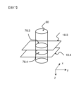
圖17顯示在柱或HAR結構處的橫截面成像方法的簡化示例。產生一系列2D橫截面影像或影像切片,其包含兩個2D橫截面影像18.3和18.4。每一者包含感興趣的半導體特徵(在此示例中為柱60)的橫截面,例如橫截面78.3和78.4。Figure 17 shows a simplified example of a cross-sectional imaging method at a pillar or HAR structure. A series of 2D cross-sectional images or image slices is generated, which contains two 2D cross-sectional images 18.3 and 18.4. Each contains a cross-section of the semiconductor feature of interest (
所描述的3D斷層造影具有幾個優點:有可能對3D結構進行整體成像。這些結構可為但不限於HAR(高外觀比)記憶體通道、FinFET、金屬線、通孔、接觸、鰭或閘極結構等。此外,有可能從任何方向將3D體積作為橫截面來查看,以可視化結構放置。換句話說,可產生任意的虛擬橫截面影像。可從3D資料集來確定3D模型,其允許從任何方向來可視化和量測3D模型中的3D特徵。另外,有可能提供2D和3D中的大量尺寸統計資料。The described 3D tomography has several advantages: It is possible to image the entire 3D structure. These structures may be, but are not limited to, HAR (high aspect ratio) memory channels, FinFETs, metal lines, vias, contacts, fins or gate structures, etc. Additionally, it is possible to view the 3D volume as a cross-section from any direction to visualize structural placement. In other words, any virtual cross-sectional image can be generated. The 3D model can be determined from a 3D data set, which allows 3D features in the 3D model to be visualized and measured from any orientation. Additionally, it is possible to provide extensive dimensional statistics in 2D and 3D.
圖7a顯示了NAND記憶體裝置的3D體積影像,其包含數個柱(包含柱60.1和60.2)。樣本體積的3D體積影像內的NAND結構包含由結構69分隔的柱或HAR結構的數個組或群組68.1或68.2。Figure 7a shows a 3D volumetric image of a NAND memory device containing several pillars (including pillars 60.1 and 60.2). The NAND structures within the 3D volumetric image of the sample volume include several groups or groups 68.1 or 68.2 of pillars or HAR structures separated by structures 69.
圖7b顯示了穿過3D體積影像的相交平面75的2D橫截面或相交影像,其平行於NAND裝置的頂表面,示出了數個柱的橫截面,包含橫截面78.1和78.2。橫截面還顯示了柱群組或HAR結構組的橫截面,如左側的柱群組79。Figure 7b shows a 2D cross-section or intersection image through an intersection plane 75 of the 3D volumetric image, parallel to the top surface of the NAND device, showing cross-sections of several pillars, including cross-sections 78.1 and 78.2. The cross section also shows a cross section of a column group or HAR structure group, such as column group 79 on the left.
在步驟S3中,選擇穿過3D體積影像的z系列相交影像。選擇可例如利用圖形使用者介面(GUI)由使用者指令來完成。舉例來說,使用者可選擇六個平面,這些六個平面形成包含柱的立方體積的邊界。在例行檢查的另一示例中,可基於程式化指令並結合3D體積影像的配準和影像分析來自動地執行選擇。可能需要使用者輸入來確認自動選擇,或者使用者可經由圖形使用者介面來執行微調。結果,選擇了一柱群組,如群組68.1或79。從3D體積影像中提取z系列相交影像,其每一者包含多個橫截面影像,例如至少一柱60、60.1或60.2的78.1或78.2。z系列相交影像平行於HAR結構的長邊方向延伸,因此平行於z方向。z系列的每個相交影像表示至少一柱60、60.1或60.2在不同的z座標處的x-y橫截面78.1或78.2。因此,z系列包含一組HAR結構或柱的相交影像。In step S3, a z-series intersecting image passing through the 3D volume image is selected. Selection may be accomplished by user instructions, such as using a graphical user interface (GUI). For example, the user can select six planes that form the boundaries of a cubic volume containing columns. In another example of a routine examination, selections may be performed automatically based on programmed instructions in conjunction with registration of 3D volumetric images and image analysis. User input may be required to confirm the automatic selection, or the user may perform fine-tuning via a graphical user interface. As a result, a column group is selected, such as group 68.1 or 79. A z-series of intersecting images is extracted from the 3D volumetric image, each of which contains a plurality of cross-sectional images, such as 78.1 or 78.2 of at least one
在一具體實施例中,以所謂的平面切片和成像方法獲取3D體積影像,其中從半導體樣本的頂層開始,逐層地銑削半導體樣本並對其進行成像。因此,由帶電粒子顯微鏡所獲得的2D影像的子集對應於包含柱的橫截面的z系列。在一具體實施例中,選擇影像區域平面視圖切片和成像方法,以包含預定的一組柱或HAR結構,且隨後獲取的3D體積影像對應於z系列的2D橫截面影像段。In a specific embodiment, the 3D volumetric images are acquired in a so-called planar slicing and imaging method, in which the semiconductor sample is milled and imaged layer by layer, starting from the top layer of the semiconductor sample. Therefore, a subset of the 2D images obtained by charged particle microscopy corresponds to the z-series containing the cross-sections of the pillars. In one embodiment, the image area plan view slices and imaging method are selected to include a predetermined set of columns or HAR structures, and the subsequently acquired 3D volumetric images correspond to a z-series of 2D cross-sectional image segments.
在步驟S4中,通過影像處理來定位在z系列的2D相交影像中的一組柱或HAR結構的橫截面。影像處理的方法可包含對比度增強、濾波、臨界操作(例如剪切)、藉由形態操作的邊緣偵測、或圖形識別或其組合或其他方法,而所有這些方法都是本技術領域中眾所周知的。結果如圖8所示,其顯示了影像處理後的一系列柱。舉例來說,識別出柱80,並藉由邊緣偵測得出柱80的輪廓82。輪廓提取的其他示例可在Li Huanliang在4th National Conference on Electrical, Electronics and Computer Engineering (NCEECE 2015), 1185 – 1189 (2016)提出的Image Contour Extraction Method based on Computer Technology(基於電腦技術的影像輪廓提取方法)中找到。圖9a顯示沿著z方向的選定柱群組中的兩個柱90.1和90.2的z系列的輪廓92的堆集。In step S4, image processing is used to locate a set of columns or cross-sections of the HAR structure in the z-series of 2D intersecting images. Image processing methods may include contrast enhancement, filtering, critical operations (such as shearing), edge detection through morphological operations, or pattern recognition or combinations thereof or other methods, all of which are well known in the art. . The results are shown in Figure 8, which shows a series of bars after image processing. For example, a pillar 80 is identified and an outline 82 of the pillar 80 is obtained through edge detection. Other examples of contour extraction can be found in the Image Contour Extraction Method based on Computer Technology proposed by Li Huanliang in the 4th National Conference on Electrical, Electronics and Computer Engineering (NCEECE 2015), 1185 – 1189 (2016) ) found in. Figure 9a shows a stacking of z-series profiles 92 of two columns 90.1 and 90.2 in a selected column group along the z-direction.
在步驟S5中,導出偏差參數,例如通過z系列的柱的橫截面的軌跡T(z)或面積A(z)。應當理解,偏差參數為參數相對於設計或理想參數的差,或為參數的變化,例如在z方向上或針對多個柱,而參數在z方向上或針對多個柱應為恆定的。In step S5, deviation parameters are derived, such as the trajectory T(z) or the area A(z) of the cross-section through the z-series of columns. It should be understood that the deviation parameter is the difference of the parameter relative to the design or ideal parameter, or the change of the parameter, such as in the z-direction or for multiple columns, while the parameter should be constant in the z-direction or for multiple columns.
首先,在z系列的一z位置計算一系列柱的數量和中心。中心可藉由以下來計算:計算柱的橫截面影像的重心、或由本技術領域中已知的幾何或分析方法來計算輪廓的中心。舉例來說,可將最佳擬合的圓形或橢圓形擬合到外部輪廓(例如輪廓82)。簡化的幾何形狀(例如圓形或橢圓形)的擬合有助於減少描述柱與理想或設計形狀之間偏差的資料量。對於圓形或橢圓形,中心是眾所周知的。從每一柱的中心和z掃描中的每一z位置,得出柱中心的相對橫向位移向量。圖10放大顯示了圖8中所示的柱的位移向量。First, calculate the number and center of a series of columns at a z position in the z series. The center may be calculated by calculating the center of gravity of a cross-sectional image of the column, or by calculating the center of the profile by geometric or analytical methods known in the art. For example, a best-fitting circle or ellipse may be fitted to the outer contour (eg, contour 82). Fitting to simplified geometries, such as circles or ellipses, helps reduce the amount of data describing the deviation of a column from its ideal or designed shape. For circles or ovals, the center is well known. From the center of each column and each z position in the z-scan, the relative lateral displacement vector of the column center is derived. Figure 10 shows an enlarged view of the displacement vector of the column shown in Figure 8.
可使用一柱的理想柱位置96來評估相對理想柱位置(顯示為點)的位移。理想的柱位置可分別從柱位置的設計或CAD資料得出,或者可藉由將規則網格最好地擬合到通過所有z平面的柱的中心的陣列來得出。CAD資料檔案可採取GDSII(圖形設計站/圖形資料系統II)格式或OASIS(開放式作品系統交換標準)格式。舉例來說,可藉由最小化位移向量的範數來實現最佳擬合。通過z系列的一個柱的剩餘位移向量(例如位移向量97)共同構成了穿過樣本的3D體積的柱的軌跡T(z)。圖11顯示了從頂層或在z方向中的不同深度,三個柱的位移向量或軌跡T(z)的x分量。The ideal column position 96 of a column can be used to evaluate the displacement from the ideal column position (shown as a point). The ideal column locations may be derived from the design or CAD data of the column locations respectively, or may be derived by best fitting a regular grid to an array passing through the center of the columns in all z-planes. CAD data files can be in GDSII (Graphics Design Station/Graphics Data System II) format or OASIS (Open Work System Interchange Standard) format. For example, the best fit can be achieved by minimizing the norm of the displacement vector. The remaining displacement vectors of a column through the z series (eg, displacement vector 97) together constitute the trajectory T(z) of the column through the 3D volume of the sample. Figure 11 shows the x-component of the displacement vector or trajectory T(z) of three columns from the top layer or at different depths in the z-direction.
在一具體實施例中,評估兩個柱n和m之間的距離Dnm(z)。如圖9a和圖9b所示,藉由幾何或分析方法,將兩個輪廓92之間的最小距離向量94計算為兩個相鄰柱90.1、90.2的兩個輪廓之間的最小距離。根據最小距離向量,可將柱通過z系列的距離Dnm(z)計算為z的純量函數。圖9b顯示了分別在兩個z位置z1和z2處的柱p2和p2或p3和p4之間的兩個最小距離向量D23(z1)或D34(z2)。鄰近度太小的相鄰結構容易受到NAND裝置的功能性或可靠性下降的影響。In a specific embodiment, the distance Dnm(z) between two pillars n and m is evaluated. As shown in Figures 9a and 9b, the minimum distance vector 94 between two profiles 92 is calculated by geometric or analytical methods as the minimum distance between the two profiles of two adjacent columns 90.1, 90.2. According to the minimum distance vector, the distance Dnm(z) of the column through the z series can be calculated as a scalar function of z. Figure 9b shows the two minimum distance vectors D23(z1) or D34(z2) between columns p2 and p2 or p3 and p4 at the two z-positions z1 and z2 respectively. Adjacent structures with too little proximity are susceptible to reduced functionality or reliability of the NAND device.
在一具體實施例中,步驟S5包含計算通過z的柱的輪廓的最佳擬合圓的半徑R(z)。可藉由最小距離方法或本技術領域已知的其他方法來執行最佳擬合圓的計算。圖12顯示了針對通過z的3個柱所獲得的半徑R(z)。In a specific embodiment, step S5 includes calculating the radius R(z) of the best-fitting circle passing through the contour of the column of z. The calculation of the best-fitting circle may be performed by the minimum distance method or other methods known in the art. Figure 12 shows the radius R(z) obtained for 3 columns passing through z.
在一具體實施例中,步驟S5包含計算對柱的輪廓最佳擬合的橢圓的偏心率E(z)。最佳擬合的橢圓的計算可藉由最小距離方法或本技術領域已知的其他方法來執行。圖13顯示了針對通過z的3個柱所獲得的偏心率E(z)。In a specific embodiment, step S5 includes calculating the eccentricity E(z) of the ellipse that best fits the contour of the column. The calculation of the best-fitting ellipse may be performed by the minimum distance method or other methods known in the art. Figure 13 shows the eccentricity E(z) obtained for 3 columns through z.
在一具體實施例中,方法步驟S5更包含對由堆集的輪廓92所包圍的表面積A(z)的評估。評估可從最佳擬合圓或最佳擬合橢圓進行解析,或藉由輪廓所覆蓋區域的數值積分來執行。在一具體實施例中,例如藉由面積A(z)的積分,可從輪廓92的這些堆疊中計算出柱的體積V。在一具體實施例中,針對每一柱計算最小面積Amin ,或計算量測面積A(z)與設計面積的偏差並將其顯示為dA(z)。In a specific embodiment, method step S5 further includes an evaluation of the surface area A(z) enclosed by the stacked contours 92 . The evaluation can be performed analytically from a best-fit circle or best-fit ellipse, or by numerical integration of the area covered by the contour. In a specific embodiment, the volume V of the column can be calculated from these stacks of profiles 92, for example by integrating the area A(z). In a specific embodiment, the minimum area A min is calculated for each column, or the deviation between the measured area A(z) and the design area is calculated and displayed as dA(z).
在一具體實施例中,接下來是步驟S6。在步驟S6中,進一步分析由步驟5所獲得的資料,例如針對統計特性、傾角或最大值或最小值。這種分析對於積體半導體裝置製造中的製程最佳化以及誤差追蹤很有用。舉例來說,藉由評估一個柱的T(z),例如藉由T(z)的梯度計算或導數,來計算柱的傾斜角。統計分析可包含對許多柱的軌跡T(z)的分析,顯示偏差Tmean (z)的平均值以及許多柱的標準偏差Tsigma (z)。圖14顯示了通過z的一組柱的平均值計算的結果,以及在z上增加的標準偏差。以相同的方式,可分析例如兩個相鄰柱的距離Dnm(z)或柱的面積A(z)或dA(z)之類的偏差。此示例說明了用於半導體電路製造的平面積體技術的穩定性,包含隨著z位置的增加而增加的平面層數量引起的誤差傳播。In a specific embodiment, step S6 follows. In step S6, the data obtained in step 5 is further analyzed, for example, for statistical characteristics, inclination angles or maximum or minimum values. This analysis is useful for process optimization and error tracking in integrated semiconductor device manufacturing. For example, the tilt angle of a column is calculated by evaluating T(z) of a column, such as by calculating the gradient or derivative of T(z). The statistical analysis may include analysis of the trajectories T(z) over many columns, showing the mean of the deviations Tmean(z) and the standard deviation Tsigma (z) over the many columns. Figure 14 shows the results calculated as the mean of a set of bars over z, with the standard deviation added over z. In the same way, deviations such as the distance Dnm(z) of two adjacent pillars or the area A(z) or dA(z) of the pillars can be analyzed. This example illustrates the stability of planar bulk technology for semiconductor circuit fabrication, including error propagation due to increasing number of planar layers with increasing z-position.
在一具體實施例中,計算偏差的最小值或最大值。作為一示例,將柱的最小面積Amin 評估為A(z)的最小值。最小面積Amin 可作為柱的電阻R的指標,其中R = ρ ∙ h / Amin 。在此,R為電阻,ρ為電阻率,h為長度,且Amin 為截面積。另一具體實施例包含對所有柱的全局最小面積Amin , g 的計算。在另一示例中,將柱的最大位移Tmax 評估為T(z)的範數的最大值;另一具體實施例包含對所有柱的全局最大偏差Tmax , g 的計算。In a specific embodiment, the minimum or maximum value of the deviation is calculated. As an example, the minimum area of the column A min is evaluated as the minimum value of A(z). The minimum area A min can be used as an indicator of the resistance R of the column, where R = ρ ∙ h / A min . Here, R is the resistance, ρ is the resistivity, h is the length, and Amin is the cross-sectional area. Another specific embodiment involves the calculation of the global minimum area Amin , g for all columns. In another example, the maximum displacement T max of a column is evaluated as the maximum value of the norm of T(z); another specific embodiment involves the calculation of the global maximum deviation T max , g of all columns.
在步驟S7中,將分析和分析結果(例如上述偏差參數)列出或儲存在檔案或記憶體中。可將偏差參數與臨界值進行比較,或可將偏差參數累積到大量檢查運行中,以產生檢查結果的資料庫。舉例來說,如果最小距離Dmin 低於臨界值,則半導體裝置中的電荷可能洩漏,且一區塊的柱可能發生故障。然而,根據本發明的方法允許在製造期間或程序開發期間使用隨機樣本來檢查半導體晶圓,且可指出與設計或目標值的偏差,從而允許程序控制或程序最佳化。根據一具體實施例,方法包含將偏差參數分類為某種類型的缺陷。此類缺陷的示例為「對準誤差」、「變形的形狀」、「距離太小」、「直徑太小」等。In step S7, the analysis and analysis results (such as the above-mentioned deviation parameters) are listed or stored in a file or memory. Deviation parameters can be compared to critical values, or deviation parameters can be accumulated over a large number of inspection runs to produce a library of inspection results. For example, if the minimum distance D min is below a critical value, charge in the semiconductor device may leak and a block of pillars may fail. However, the method according to the present invention allows the use of random samples to inspect semiconductor wafers during manufacturing or during program development and can indicate deviations from design or target values, thereby allowing program control or program optimization. According to a specific embodiment, the method includes classifying the deviation parameter as a defect of a certain type. Examples of such defects are "alignment error", "deformed shape", "distance too small", "diameter too small", etc.
在一具體實施例中,評估柱的局部缺陷,例如用錯誤的材料填充、顆粒缺陷、污染或任何其他缺陷,這些缺陷導致圓周橫截面的局部偏差,在下文中也稱作夾雜物。在圖15a中顯示了一示例。兩柱在其橫截面101.1、101.2中顯示了此類夾雜物102.1、102.3。夾雜物可擴展到z系列相交影像中的幾個相交影像上。在輪廓提取後(如圖15b所示),提取了輪廓103.1和103.2以及夾雜物104.1和104.2的面積。有缺陷的柱進一步以標記「x」標識。夾雜物104.1和104.2的面積會增加柱的外表面輪廓的粗糙度,並可能為故障的來源。舉例來說,將夾雜物104.1和104.2與參考夾雜物進行比較,以確定裝置是否發生故障或正常工作。在一具體實施例中,評估整個一組柱中的夾雜物或標記的數量,並因此在一組製造的半導體樣本上得出了程序誤差率以及例如進行監視。In a specific embodiment, the column is evaluated for local defects, such as filling with the wrong material, particle defects, contamination or any other defects that lead to local deviations of the circumferential cross-section, also referred to as inclusions in the following. An example is shown in Figure 15a. Both columns show such inclusions 102.1, 102.3 in their cross-sections 101.1, 101.2. Inclusions can be extended to several intersecting images in the z-series of intersecting images. After contour extraction (as shown in Figure 15b), the areas of contours 103.1 and 103.2 and inclusions 104.1 and 104.2 are extracted. Defective columns are further identified with an "x" mark. The area of inclusions 104.1 and 104.2 will increase the roughness of the outer surface profile of the column and may be a source of failure. For example, inclusions 104.1 and 104.2 are compared to reference inclusions to determine if the device is malfunctioning or functioning properly. In a specific embodiment, the number of inclusions or marks in an entire set of pillars is evaluated and thus the process error rate is derived and monitored, for example, on a set of fabricated semiconductor samples.
在一具體實施例中,進一步分析內部柱結構。柱包含例如內部通道和由不同的導電或半導電材料製成的圍繞內部通道的多個層。舉例來說,核心通道周圍的數個層可包含隧道層、隔離層、電荷陷阱層、和阻擋層。在每個相交影像中,這些層藉由其材料對比度進行識別,且可按照與上述相同的方式進行分析,例如外部輪廓或輪廓,可得出層的環形區域的軌跡。圖16a顯示了一柱陣列的高解析度相交影像的示例,其由SEM在高解析度模式下所獲得。圖中顯示了在3行109.1、109.2和109.3中的一組柱。在行109.3中的一柱105的示例中,顯示了核心106、第一中間層107和第二外部層108;第二外部層108和第一中間層107由隔離層110隔開。圖16b分別顯示了所提取的柱105的輪廓組115的核心106及層107及108的輪廓116、117和118,以及一些其他柱的輪廓,例如相鄰柱的輪廓組111、112。In a specific embodiment, the internal column structure is further analyzed. A pillar contains, for example, an internal channel and multiple layers surrounding the internal channel made of different conductive or semiconductive materials. For example, the layers surrounding the core channel may include tunnel layers, isolation layers, charge trap layers, and barrier layers. In each intersecting image, the layers are identified by their material contrast and can be analyzed in the same way as above, such as outer contours or contours, which lead to the locus of annular areas of the layer. Figure 16a shows an example of a high-resolution intersection image of a pillar array, obtained by a SEM in high-resolution mode. The diagram shows a set of bars in 3 rows 109.1, 109.2 and 109.3. In the example of a column 105 in row 109.3, a core 106, a first intermediate layer 107 and a second outer layer 108 are shown; the second outer layer 108 and the first intermediate layer 107 are separated by an isolation layer 110. Figure 16b shows the extracted core 106 of the profile group 115 of the column 105 and the profiles 116, 117 and 118 of the layers 107 and 108 respectively, as well as the profiles of some other columns, such as the profile groups 111, 112 of adjacent columns.
對於每組輪廓,核心和層的軌跡TC(z)、TL1(z)、TL2(z)、…以及柱的核心和層的相應面積AC(z)、AL1(z)、AL2(z)、…可按照與上述針對外部輪廓相同的方式進行計算。以與上述相同的方式,可以計算各層之間的內部距離,並可得出最小厚度或距離。圖16c在示例中顯示了針對輪廓116、117和118的相對於核心TC(z)的軌跡的半徑RC(z)、RL1(z)和RL2(z)。如上述,可藉由統計方法來分析一組柱的所有產生的參數。而且,可偵測並算出可能導致洩漏的層中的局部缺陷。這允許對特徵化柱內部結構的大量資料進行詳細的統計分析,例如核心和層的局部缺陷或夾雜物、或核心和層之間的距離。For each set of contours, the trajectories of the core and layers TC(z), TL1(z), TL2(z), ... and the corresponding areas of the core and layers of the column AC(z), AL1(z), AL2(z), …can be calculated in the same way as above for the outer contour. In the same way as above, the internal distance between layers can be calculated and the minimum thickness or distance can be derived. Figure 16c shows in an example the radii RC(z), RL1(z) and RL2(z) relative to the trajectory of the core TC(z) for the contours 116, 117 and 118. As mentioned above, all resulting parameters of a set of columns can be analyzed by statistical methods. Furthermore, local defects in the layer that could lead to leaks can be detected and accounted for. This allows detailed statistical analysis of a large amount of information that characterizes the internal structure of the column, such as local defects or inclusions in the core and layers, or the distance between the core and layers.
上述方法可藉由能夠處理巨大圖形資料集的專用計算系統來執行。本發明的方法係實現為電腦程式產品並儲存在專用計算系統的內部記憶體中。控制器控制顯微鏡(例如交叉光束顯微鏡1)的操作,並將由顯微鏡產生的影像資料傳送到處理單元(例如圖形處理器單元(GPU)),控制器進一步控制以根據方法步驟S2至S6處理影像資料,控制器進一步控制以產生結果並將其儲存在記憶體裝置(例如,快閃、隨機存取記憶體(RAM)、唯讀記憶體(ROM)、或其他合適的變化形式)。控制器係組態以根據電腦程式碼自動地操作系統。電腦程式碼實施於非暫態電腦可讀媒體中,並程式化以執行如上所述的任何數量的功能或演算法。電腦程式碼進一步組態為:控制器不時通過圖形使用者介面(GUI)通知使用者需要使用者輸入。控制器將系統設定為等待狀態,直到執行使用者輸入為止。這樣的使用者輸入可例如為藉由影像處理器執行的z系列2D橫截面影像的區域選擇或對z系列2D橫截面影像的區域選擇的確認。在步驟S7中,以標準輸出檔案格式或藉由圖形使用者介面進一步輸出結果,例如儲存在記憶體裝置中的偏差參數。The above methods can be performed by specialized computing systems capable of handling huge graphics data sets. The method of the present invention is implemented as a computer program product and stored in the internal memory of a dedicated computing system. The controller controls the operation of the microscope (e.g., cross-beam microscope 1) and transmits image data generated by the microscope to a processing unit (e.g., graphics processor unit (GPU)). The controller further controls to process the image data according to method steps S2 to S6. , the controller further controls to generate results and store them in a memory device (eg, flash, random access memory (RAM), read only memory (ROM), or other suitable variations). The controller is configured to automatically operate the system based on computer program code. Computer code is embodied in non-transitory computer-readable media and programmed to perform any number of functions or algorithms as described above. The computer code is further configured such that the controller notifies the user that user input is required from time to time through a graphical user interface (GUI). The controller sets the system to wait until user input is performed. Such user input may be, for example, a region selection of a z-series 2D cross-sectional image or a confirmation of a region selection of a z-series 2D cross-sectional image performed by the image processor. In step S7, the results are further output in a standard output file format or through a graphical user interface, such as deviation parameters stored in a memory device.
在檢查或審查應用中,在由複數個橫截面影像切片形成的3D資料堆集的分析過程中,需要高度自動化。在本發明的一具體實施例中,提供了一種自動化的工作流程,用於在裝置(例如3D記憶體晶片(VNAND或3DRAM))的生產期間對半導體晶圓進行3D檢查。舉例來說,3D記憶體晶片由彼此平行的許多柱狀結構所組成,有時也稱作記憶體通道或「柱」。可使用FIB-SEM顯微鏡,以橫截面成像技術來研究包含這種3D記憶體裝置的樣本。在一切片中的柱的覆蓋區的典型數量可達到幾百個,甚至多達1000個或更多。典型的影像切片堆集可包含數百個影像。在大多數應用中,在以3D重建柱時,高度自動化是必不可少的。In inspection or review applications, a high degree of automation is required during the analysis of 3D data accumulations formed from multiple cross-sectional image slices. In a specific embodiment of the present invention, an automated workflow is provided for 3D inspection of semiconductor wafers during the production of devices such as 3D memory wafers (VNAND or 3DRAM). For example, a 3D memory chip is composed of many parallel columnar structures, sometimes called memory channels or "pillars." Samples containing such 3D memory devices can be studied with cross-sectional imaging using FIB-SEM microscopy. The typical number of column footprints in any slice can reach several hundred, or even as many as 1000 or more. A typical image tile stack can contain hundreds of images. In most applications, a high degree of automation is essential when reconstructing columns in 3D.
一個影像切片中的柱或其他半導體結構的覆蓋區的典型數量可達到幾百個,甚至多達1000個或更多。典型的3D資料堆集可包含數百個橫截面影像切片。因此,2D橫截面影像的3D堆集可包含超過柱的100.000的橫截面。另一方面,解析度低於2 nm的每個10µm x 10µm的2D影像切片都可輕鬆包含超過5個十億像素,甚至超過10個十億像素。從這個大量的3D體積影像資料中,推導出幾個參數,例如柱的大約100.000橫截面的中心位置、半徑和橢圓率,並提取約500.000數值。藉由使用例如擬合演算法和統計方法對數值進行分析,可實現進一步的縮減,並提供了重要的性能指標。性能指標的示例為偏差參數(例如橫截面面積的偏差)的最大值、兩柱之間的最小距離、複數個柱內的一柱的最大傾斜度、以及複數個柱的最大擺動參數、以及這些參數中任何一個的變化的描述符(例如統計方差)。根據自動化工作流程的具體實施例,以高產出量分析了柱或一般半導體結構的多達數千個影像橫截面。根據具體實施例的方法的細節將以3D記憶體晶片中的柱或HAR結構的示例來作描述,但方法通常適用於任何類型的半導體和晶圓。The typical number of footprints of pillars or other semiconductor structures in an image slice can be in the hundreds, or even as many as 1,000 or more. A typical 3D data collection can contain hundreds of cross-sectional image slices. Therefore, a 3D stack of 2D cross-section images can contain more than 100.000 cross-sections of columns. On the other hand, each 10µm x 10µm 2D image slice with resolutions below 2 nm can easily contain more than 5 gigapixels, and even more than 10 gigapixels. From this large amount of 3D volumetric imaging data, several parameters were derived, such as the center position, radius and ellipticity of approximately 100.000 cross-sections of the column, and approximately 500.000 values were extracted. By analyzing the values using, for example, fitting algorithms and statistical methods, further reductions are achieved and important performance indicators are provided. Examples of performance indicators are the maximum value of a deviation parameter (such as the deviation of the cross-sectional area), the minimum distance between two columns, the maximum inclination of a column within a plurality of columns, and the maximum swing parameter of a plurality of columns, and these A descriptor of variation in any one of the parameters (e.g. statistical variance). According to specific embodiments of the automated workflow, up to thousands of image cross-sections of pillars or general semiconductor structures are analyzed with high throughput. Details of methods according to specific embodiments will be described with the example of pillars or HAR structures in 3D memory wafers, but the methods are generally applicable to any type of semiconductor and wafer.
根據具體實施例的方法包含減少3D體積影像內的資料量的幾個步驟。在自動偵測每個切片中的柱覆蓋區以及自動產生一些描述性參數(例如中心位置、最佳擬合半徑、橢圓率)的第一步驟中,約M = 10 Gigapixel或更多的大量像素減少到約N2 = 500.000第一數值。舉例來說,提取位於影像切片內的柱的交點處的中心座標的X座標和Y座標的列表。分析第一數值,並從例如中心位置得出每個柱的單一傾斜角度,並達成縮減至約N3 = 10.000第二數值。藉由統計方法進一步處理第二數值,並進一步降低到例如低於10個性能指標。第一示例使用古典的影像處理技術,而第二示例使用基於機器學習(基於ML)的方法。根據具體實施例的方法需要用於半導體裝置的自動檢查的準備步驟。Methods according to specific embodiments include several steps to reduce the amount of data within a 3D volumetric image. In the first step of automatically detecting the column footprint in each slice and automatically generating some descriptive parameters (e.g. center position, best fit radius, ellipticity), a large number of pixels of about M = 10 Gigapixel or more Reduce to a first value of approximately N2 = 500.000. For example, extract a list of X-coordinates and Y-coordinates of the center coordinates located at the intersection of the cylinders within the image slice. The first value is analyzed and a single tilt angle is derived for each column from, for example, the center position, and a second value reduced to approximately N3 = 10.000 is achieved. The second value is further processed by statistical methods and further reduced to, for example, less than 10 performance indicators. The first example uses classical image processing techniques, while the second example uses a machine learning (ML-based) approach. Methods according to specific embodiments require preparatory steps for automated inspection of semiconductor devices.
晶圓檢查的工作流程示例包含對半導體特徵的重建,其可應用於使用上述FIB-SEM顯微鏡所獲得的3D體積影像上。一示例包含使用古典影像處理技術進行自動檢查的準備步驟,如圖18所示。在第一步驟C1中,例如藉由根據上述步驟S1和S2的方法產生代表性的3D體積影像資料。在影像獲取的步驟C1期間,例如以對準基準點或其他影像對準的方法將2D橫截面影像切片彼此對準。相鄰2D橫截面影像之間的殘餘對準誤差或偏移很小,且不超過預定的對準臨界值。在步驟C1之前,方法可包含以下步驟:將晶圓裝載到晶圓台上,晶圓對齊和配準,在晶圓表面上形成基準特徵,使用例如FIB或LASER光束產生溝槽,以及從晶圓上提取至少一樣本,例如利用探針(樣本附著在其上)。它可更包含將樣本定位在保持架上的步驟,該保持架可在FIB與雙光束檢查裝置的帶電粒子成像裝置的交叉處移動和定位。An example workflow for wafer inspection involves the reconstruction of semiconductor features that can be applied to 3D volumetric images obtained using the FIB-SEM microscope described above. An example includes preparatory steps for automated inspection using classical image processing techniques, as shown in Figure 18. In the first step C1, representative 3D volumetric image data is generated, for example, by the method according to the above-mentioned steps S1 and S2. During the image acquisition step C1, the 2D cross-sectional image slices are aligned with each other, for example by aligning to fiducial points or other image alignment methods. The residual alignment error or offset between adjacent 2D cross-sectional images is small and does not exceed a predetermined alignment threshold. Prior to step C1, the method may include the steps of loading the wafer onto a wafer stage, aligning and registering the wafer, forming fiducial features on the wafer surface, generating trenches using, for example, a FIB or LASER beam, and removing the wafer from the wafer. At least one sample is extracted from the circle, for example using a probe (to which the sample is attached). It may further include the step of positioning the sample on a holder that can be moved and positioned at the intersection of the FIB and the charged particle imaging device of the dual-beam inspection device.
在2D橫截面影像段或覆蓋區的註記的準備步驟C2中,例如,感興趣的柱覆蓋區由操作員註記。一或多個覆蓋區由操作員註記,以產生用於交叉相關的模板或訓練基於ML的物體偵測器。在註記步驟期間,使用者以交互方式註記一或多個切片中的一或多個覆蓋區。在一示例中,註記由圖形使用者介面輔助,其係組態以例如在由操作員使用電腦滑鼠或其他輸入裝置在2D橫截面影像的顯示器上選擇的位置處顯示一矩形或圓形。在一示例中,註記由影像處理演算法輔助以用於覆蓋區偵測。這類的演算法可包含濾波器操作、邊緣偵測或輪廓提取、或形態操作。在一示例中,用於覆蓋區偵測的演算法利用儲存在資料庫中的先前獲得的模板來執行交叉相關的操作或基於機器學習(「ML」)的物體偵測器,以幫助操作員選擇感興趣的橫截面影像段。In the preparation step C2 of the annotation of the 2D cross-sectional image segments or footprints, for example, column footprints of interest are annotated by the operator. One or more footprints are annotated by the operator to generate templates for cross-correlation or to train ML-based object detectors. During the annotation step, the user interactively annotates one or more footprints in one or more slices. In one example, annotation is assisted by a graphical user interface configured to display, for example, a rectangle or circle at a location selected on a display of a 2D cross-sectional image by an operator using a computer mouse or other input device. In one example, annotation is assisted by image processing algorithms for coverage detection. Such algorithms may include filter operations, edge detection or contour extraction, or morphological operations. In one example, algorithms for coverage area detection utilize previously obtained templates stored in a database to perform cross-correlation operations or machine learning ("ML") based object detectors to assist operators. Select the cross-sectional image segment of interest.
在步驟C3或模板產生步驟中,產生表示感興趣的半導體結構的橫截面影像特徵的模板。模板例如為理想化的橫截面影像特徵,其組態用於交叉相關。在一示例中,從步驟C2的註記覆蓋區導出模板或理想化的橫截面影像特徵。舉例來說,步驟C2的註記覆蓋區會自動對準並平均。另外,可應用例如降噪或銳化的影像處理技術。因此,模板是代表感興趣的半導體結構(例如HAR結構或柱)的「典型」或平均覆蓋區的影像。在模板的產生期間,確定模板的代表性中心位置,且相對於代表性中心位置調整模板影像。在一示例中,考慮數個感興趣的半導體結構,並對數個感興趣的半導體結構執行步驟C2和C3,以產生代表第一感興趣的半導體結構的至少一第一模板以及代表感興趣的半導體結構的第二模板。In step C3 or the template generation step, a template representing cross-sectional image features of the semiconductor structure of interest is generated. The template is, for example, an idealized cross-sectional image feature configured for cross-correlation. In one example, templates or idealized cross-sectional image features are derived from the annotation footprint of step C2. For example, the annotation footprint in step C2 is automatically aligned and averaged. Additionally, image processing techniques such as noise reduction or sharpening may be applied. Thus, a template is an image that represents a "typical" or average footprint of a semiconductor structure of interest, such as a HAR structure or pillar. During the generation of the template, a representative center position of the template is determined, and the template image is adjusted relative to the representative center position. In an example, a plurality of semiconductor structures of interest are considered, and steps C2 and C3 are performed on the plurality of semiconductor structures of interest to generate at least a first template representing a first semiconductor structure of interest and a first template representing the semiconductor structure of interest. The second template of the structure.
在步驟C4中,執行一系列交叉相關。執行2D橫截面影像切片與在步驟C3中所產生的模板的交叉相關。所產生的2D交叉相關影像中的每個峰值(每個2D橫截面影像切片中模板的每一匹配位置有一個)表示所偵測到的感興趣半導體結構的覆蓋區或橫截面。為了提高覆蓋區偵測的敏感度及/或穩固性,可使用代表感興趣的第一半導體結構的不同模板來多次執行交叉相關。可例如在每次交叉相關操作之前使用一系列縮放因子來縮放代表感興趣的第一半導體結構的模板的改變。另外,不同的模板可用於不同的橫截面影像切片或例如3D體積影像中的不同的z位置。In step C4, a series of cross-correlation is performed. Cross-correlation of the 2D cross-sectional image slices with the template generated in step C3 is performed. Each peak in the resulting 2D cross-correlation image (one for each match position of the template in each 2D cross-sectional image slice) represents the detected footprint or cross-section of the semiconductor structure of interest. In order to increase the sensitivity and/or robustness of coverage detection, cross-correlation can be performed multiple times using different templates representing the first semiconductor structure of interest. Changes in the template representing the first semiconductor structure of interest may be scaled, for example, using a series of scaling factors before each cross-correlation operation. Additionally, different templates can be used for different cross-sectional image slices or different z-positions in eg 3D volumetric images.
在步驟C5中,產生通道覆蓋區的列表覆蓋區座標或中心座標,其與在每一2D影像橫截面影像切片中在步驟C4中偵測到的覆蓋區相對應。從2D影像橫截面影像切片中的橫向或x-y位置得出橫向座標,且從3D體積內的2D影像橫截面影像切片的z位置得出3D體積影像中的z座標。在步驟C4中在2D橫截面影像切片中偵測到的感興趣的半導體結構的2D橫截面影像特徵的中心位置對應在步驟C3中確定的模板的代表性中心位置。In step C5, a list of footprint coordinates or center coordinates of the channel footprint is generated, which corresponds to the footprint detected in step C4 in each 2D image cross-sectional image slice. The lateral coordinate is derived from the lateral or x-y position in the 2D image cross-sectional image slice, and the z-coordinate in the 3D volume image is derived from the z-position of the 2D image cross-sectional image slice within the 3D volume. The center position of the 2D cross-sectional image feature of the semiconductor structure of interest detected in the 2D cross-sectional image slice in step C4 corresponds to the representative center position of the template determined in step C3.
在步驟C6中,將代表覆蓋區的2D截面影像特徵進行分割,亦即確定覆蓋區的邊界。這是針對個別覆蓋區「局部地」完成,亦即使用複數個2D子影像,每個子影像在步驟C5中所確定的中心位置處僅包含一覆蓋區。使用用於輪廓提取的已知演算法來計算邊界,例如邊緣偵測、形態操作、閾值化或等效方法。In step C6, the 2D cross-sectional image features representing the coverage area are segmented, that is, the boundary of the coverage area is determined. This is done "locally" for individual coverage areas, that is, using a plurality of 2D sub-images, each of which contains only one coverage area at the center position determined in step C5. Boundaries are calculated using known algorithms for contour extraction, such as edge detection, morphological operations, thresholding, or equivalent methods.
在步驟C7中,將在步驟C6中確定的輪廓或邊界分配給感興趣的半導體結構,例如個別HAR結構或柱。屬於相鄰2D橫截面影像切片中的相同柱/通道的在步驟C6中計算的邊界或輪廓係例如根據其橫向中心座標來確定。因此,對於每個感興趣的半導體結構,產生在不同的2D橫截面影像切片中屬於該感興趣半導體結構的輪廓/邊界的列表。In step C7, the contours or boundaries determined in step C6 are assigned to semiconductor structures of interest, such as individual HAR structures or pillars. The boundaries or contours calculated in step C6 belonging to the same column/channel in adjacent 2D cross-sectional image slices are determined, for example, based on their lateral center coordinates. Thus, for each semiconductor structure of interest, a list of contours/boundaries belonging to that semiconductor structure of interest in different 2D cross-sectional image slices is generated.
步驟C1的預定對準臨界值可例如為兩個相鄰覆蓋區之間的距離的一半。在這種情況下,避免了將輪廓分配給感興趣的相應半導體結構的任何歧義。然而,在示例中,並非總是能夠識別和分配屬於相同的感興趣的半導體結構的輪廓。在此示例中,不能明確分配給感興趣的半導體結構的2D橫截面影像特徵的輪廓被標記為模糊的。The predetermined alignment threshold of step C1 may be, for example, half the distance between two adjacent coverage areas. In this case, any ambiguity in assigning contours to the corresponding semiconductor structures of interest is avoided. However, in the examples it is not always possible to identify and assign contours belonging to the same semiconductor structure of interest. In this example, contours of 2D cross-sectional image features that cannot be clearly assigned to the semiconductor structure of interest are marked as ambiguous.
在步驟C8中,分析屬於相同的感興趣的半導體結構的覆蓋區(其在步驟C7中已在不同的2D橫截面影像切片中識別出),並選擇性地改善了2D橫截面影像切片相對於彼此的橫向對準。為此目的,針對所有成對的相鄰2D橫截面影像切片,計算在一2D橫截面影像切片中的所有覆蓋區相對於在一相鄰2D橫截面影像切片中的相應覆蓋區的平均偏移。接著,將計算出的偏移應用於覆蓋區的相應中心座標。步驟C8的結果為一組列表,每一列表包含屬於感興趣的特定半導體結構(例如,HAR通道或柱)的校正中心位置和輪廓/邊界。In step C8, the footprints belonging to the same semiconductor structure of interest (which have been identified in the different 2D cross-sectional image slices in step C7) are analyzed and selectively improved with respect to the 2D cross-sectional image slices Lateral alignment with each other. For this purpose, for all pairs of adjacent 2D cross-sectional image slices, the average offset of all footprints in a 2D cross-sectional image slice relative to the corresponding footprint in an adjacent 2D cross-sectional image slice is calculated . Next, the calculated offset is applied to the corresponding center coordinates of the coverage area. The result of step C8 is a set of lists, each list containing corrected center positions and contours/boundaries belonging to a particular semiconductor structure of interest (eg, HAR channel or pillar).
在示例中,在2D橫截面影像切片中以精確對準來考慮偏移,且對於在步驟C7中被標記為模糊的輪廓重複分配步驟C7。In the example, the offset is taken into account with precise alignment in the 2D cross-sectional image slices, and step C7 is assigned repeatedly for the contours marked as blurred in step C7.
在步驟C9(3D表面產生)中,對於每個通道,輪廓座標被提取為X-Y-和Z-座標,作為位於感興趣的特定半導體結構的表面上的表面點。表面點也可組合至原始形式,例如用於可視化或進一步分析的三角形網格或3D多邊形輪廓。因此,大量的表面或輪廓座標被簡化為由一組參數描述的預定基元或基元形式,其表示感興趣的半導體結構及其與理想形狀的預定典型偏差。基元可為傾斜或扭曲的圓柱體,其傾斜角和擺動由很少的參數來描述。In step C9 (3D surface generation), for each channel, the contour coordinates are extracted as X-Y- and Z-coordinates as surface points located on the surface of the specific semiconductor structure of interest. Surface points can also be combined into raw forms such as triangular meshes or 3D polygonal outlines for visualization or further analysis. Therefore, a large number of surface or contour coordinates are reduced to predetermined primitives or primitive forms described by a set of parameters, which represent the semiconductor structure of interest and its predetermined typical deviations from the ideal shape. The primitive can be a tilted or twisted cylinder, whose tilt angle and oscillation are described by a few parameters.
在步驟C10中,對感興趣的半導體結構進行定量特徵化。對於每個感興趣的半導體結構,提取或導出特徵化整個感興趣的半導體結構(例如,HAR結構或柱)的幾何形狀的一組參數。這類參數的示例是柱的平均半徑和橢圓率,以及參數對Z座標的相依性、柱軸的傾斜度和曲率、感興趣的相鄰半導體結構之間的接近度或最接近距離。可計算大量柱(例如,資料集中所有柱的統計特性) 的統計特性。這樣的特性的示例為一組柱的平均半徑及其標準偏差、柱的平均傾斜度、相鄰柱的平均接近度、或複數個柱上的參數的最大值和最小值。本技術領域中具有通常知識者可定義表示性能指標的複數個其他統計資訊,例如適合於監視專用製造程序步驟或適合於確定所製造的半導體裝置的代表性性能。步驟C10的結果也可與從同一晶圓或第二晶圓提取的其他樣本的其他檢查量測結果相關聯,或與從其製備樣本的晶圓上的位置相關聯。舉例來說,示例為柱的橫截面隨深度的變化、柱的傾斜(特別是在晶圓的邊緣處朝向晶圓的外圓周)、晶圓上傾斜角的變化。其他示例為柱的形狀,例如桶形的平均數量。結果,例如代表性基元也可與例如從半導體裝置的設計的CAD資料所獲得的參考基元進行比較。In step C10, the semiconductor structure of interest is quantitatively characterized. For each semiconductor structure of interest, a set of parameters characterizing the geometry of the entire semiconductor structure of interest (eg, HAR structures or pillars) is extracted or derived. Examples of such parameters are the mean radius and ellipticity of the cylinder, as well as the dependence of the parameters on the Z coordinate, the inclination and curvature of the cylinder axis, the proximity or closest distance between adjacent semiconductor structures of interest. Statistical properties can be calculated for a large number of bars (for example, the statistical properties of all bars in a data set). Examples of such properties are the average radius of a set of columns and its standard deviation, the average tilt of columns, the average proximity of adjacent columns, or the maximum and minimum values of a parameter over a plurality of columns. One of ordinary skill in the art may define a plurality of other statistics representative of performance indicators, such as may be suitable for monitoring specific manufacturing process steps or may be suitable for determining representative performance of fabricated semiconductor devices. The results of step C10 may also be correlated with other inspection measurements of other samples taken from the same wafer or a second wafer, or with the location on the wafer from which the sample was prepared. Examples are, for example, the change in the cross-section of the pillars with depth, the tilt of the pillars (especially at the edge of the wafer towards the outer circumference of the wafer), the variation of the tilt angle on the wafer. Other examples are the shape of the bars, such as the average number of barrels. As a result, for example representative primitives may also be compared with reference primitives obtained for example from CAD data of a design of a semiconductor device.
在具體實施例的示例中,應用了基於機器學習(「ML」)的物體偵測器。代替如步驟C3中所描述的產生模板,在修改的步驟C3M中,使用在步驟C2中標識的已註記橫截面影像特徵來訓練機器學習演算法。接著,在修改的步驟C4M中應用機器學習算法,以自動偵測感興趣的半導體結構的橫截面影像特徵。In an example of a specific embodiment, a machine learning ("ML") based object detector is applied. Instead of generating a template as described in step C3, in a modified step C3M, the annotated cross-sectional image features identified in step C2 are used to train the machine learning algorithm. Next, a machine learning algorithm is applied in a modified step C4M to automatically detect cross-sectional image features of the semiconductor structure of interest.
檢查方法也可進一步包含利用基於機器學習(ML)的局部分割的修改步驟C6M。在先前步驟中確定覆蓋區的座標之後,確定覆蓋區的邊界或輪廓,接著將覆蓋區分割並與背景分離。邊界或輪廓也可藉由使用基於ML的分割演算法來計算。The inspection method may also further comprise a modified step C6M utilizing machine learning (ML) based local segmentation. After determining the coordinates of the footprint in the previous step, the boundaries or contours of the footprint are determined, and then the footprint is segmented and separated from the background. Boundaries or contours can also be calculated by using ML-based segmentation algorithms.
從上面的描述可清楚地看出,步驟C2和C3是準備步驟,且被執行以準備常規檢查任務。在例行檢查任務中,省略了步驟C2和C3,而是將在準備工作流程中所確定並例如儲存在資料庫中的一組預選模板用於步驟C4及以後的步驟。還應理解到,在常規檢查期間,步驟可以重疊。舉例來說,步驟C4可與步驟C1重疊,且可例如使用在步驟C1期間所獲得的第一2D橫截面影像開始進行藉由與模板相關聯來識別覆蓋區。某些程序步驟也可能以更改的順序來執行。舉例來說,可例如在精細對準的步驟C8之前,在一組代表性的感興趣的半導體結構上執行3D表面產生的步驟C9,且根據步驟C8的精細對準的執行可能受到代表性3D表面的分析結果的影響。精細對準的步驟C8也可能在步驟C5之後直接執行。As is clear from the above description, steps C2 and C3 are preparatory steps and are performed to prepare for routine inspection tasks. In routine inspection tasks, steps C2 and C3 are omitted, but a set of preselected templates determined in the preparatory workflow and stored, for example, in a database are used for step C4 and subsequent steps. It should also be understood that during routine inspections, steps may overlap. For example, step C4 may overlap with step C1 and may begin by identifying the footprint by association with a template, eg using the first 2D cross-sectional image obtained during step C1 . Certain program steps may also be performed in a changed order. For example, the step C9 of 3D surface generation may be performed on a representative set of semiconductor structures of interest, eg before the step C8 of fine alignment, and the performance of the fine alignment according to step C8 may be affected by the representative 3D Impact on surface analysis results. The fine alignment step C8 may also be performed directly after step C5.
包含步驟C4至C10中的任何一個或包含修改後的步驟C4M或C6M的方法得益於更快的計算時間。在該方法中,在第一步驟中,3D體積影像的體積資料量減少到比第一數值少10000倍以上。第一數值包含感興趣的半導體結構的中心位置和輪廓座標的列表,例如在步驟C5至C7中獲得的。在步驟C9期間,將第一數值進一步減小為代表性基元形式(representative primitive form)的參數。由此,第一數值的數量進一步減小50倍為第二數值。該方法進一步受益於統計平均,包含在代表性基元的產生期間的步驟C9的統計平均。Methods containing any one of steps C4 to C10 or containing modified steps C4M or C6M benefit from faster calculation times. In this method, in the first step, the volume data amount of the 3D volume image is reduced to more than 10,000 times less than the first value. The first value contains a list of center positions and outline coordinates of the semiconductor structure of interest, for example obtained in steps C5 to C7. During step C9, the first value is further reduced to a parameter in a representative primitive form. Thus, the number of the first numerical value is further reduced by 50 times to the second numerical value. The method further benefits from statistical averaging included in step C9 during the generation of representative primitives.
上述示例在作為感興趣的半導體結構的HAR通道或柱的示例中進行了說明。其他感興趣的半導體結構可為邏輯探針中的通孔。通孔為包含各種IC元件的邏輯晶片的相鄰水平層之間的垂直接觸結構。可使用與3D記憶體探針中的HAR通道或柱相同的方式處理此類過孔。其他示例為邏輯晶片中的金屬線或連接。可使用與3D記憶體晶片中的記憶體通道相同的方式來處理一系列這種金屬線,其已知為(例如,從可得的設計資訊)彼此平行的。The above examples are illustrated in the example of HAR channels or pillars as semiconductor structures of interest. Other semiconductor structures of interest may be vias in logic probes. Vias are vertical contact structures between adjacent horizontal layers of a logic die containing various IC components. Such vias can be treated in the same way as HAR channels or posts in 3D memory probes. Other examples are metal lines or connections in logic chips. A series of such metal lines, which are known (eg from available design information) to be parallel to each other, can be processed in the same way as memory channels in a 3D memory chip.
根據本發明的方法可用於半導體裝置的製程開發或製造的製造程序特徵化、製造程序最佳化或/和製造程序監視。The method according to the present invention can be used for manufacturing process characterization, manufacturing process optimization, or/and manufacturing process monitoring for process development or manufacturing of semiconductor devices.
上述具體實施例可完全或部分地彼此組合。同樣,本領域技術人員已知的方法、導出參數或統計值的修改在本發明的範疇內是可能的。儘管以順序S1至S5來解釋根據圖5的方法,但至少兩方法步驟的順序(例如方法步驟S2和S3的順序)是可交換。The specific embodiments described above may be completely or partially combined with each other. Likewise, modifications of methods, derived parameters or statistical values known to those skilled in the art are possible within the scope of the invention. Although the method according to FIG. 5 is explained in the sequence S1 to S5, the sequence of at least two method steps, for example the sequence of method steps S2 and S3, is interchangeable.
1:交叉光束顯微鏡 2:橫截面 3:橫截面 4:橫截面 5:聚焦離子束 6:角度 7:電子束 8:掃描成像線 9:離子束 10:塊狀樣本 11:橫截面表面 18:橫截面影像 18.3、18.4:橫截面影像 20:橫截面影像 50:積體半導體 51:矽基板 52:頂表面 54.1-54.z:層 55:通孔 56:金屬結構 57:閘極 58:摻雜結構 59:接觸 60:柱 60.1、60.2:柱 62:柱段 63:細間隙 64:軌跡 66:外輪廓 68.1、68.2:柱群組 69:結構 70:角度 72.1-72.3:柱段 74.1、74.2:軌跡 75:相交平面 76.1、76.2:輪廓 78.1、78.2:橫截面 78.3、78.4:橫截面 79:群組 80:柱 82:輪廓 90.1、90.2:柱 92:輪廓 94:最小距離向量 96:理想柱位置 97:位移向量 101.1、101.2:橫截面 102.1、102.2:夾雜物 103.1、103.2:輪廓 104.1、104.2:夾雜物 105:柱 106:核心 107:層 108:層 109.1、109.2、109.3:行 110:隔離層 111:輪廓組 112:輪廓組 115:輪廓組 116:輪廓 117:輪廓 118:輪廓1:Crossed beam microscope 2: Cross section 3: Cross section 4: Cross section 5: Focused ion beam 6:Angle 7: Electron beam 8:Scan imaging line 9:Ion beam 10: Block sample 11: Cross-sectional surface 18: Cross-sectional image 18.3, 18.4: Cross-sectional image 20: Cross-sectional image 50:Integrated semiconductor 51:Silicon substrate 52:Top surface 54.1-54.z: layer 55:Through hole 56:Metal structure 57: Gate 58: Doping structure 59:Contact 60: column 60.1, 60.2: Column 62: Column segment 63: fine gap 64:Trajectory 66:Outer contour 68.1, 68.2: Column group 69: Structure 70:Angle 72.1-72.3: Column section 74.1, 74.2: trajectory 75: Intersecting planes 76.1, 76.2:Contour 78.1, 78.2: Cross section 78.3, 78.4: Cross section 79:Group 80: column 82:Contour 90.1, 90.2: Column 92:Contour 94: Minimum distance vector 96:Ideal column position 97: Displacement vector 101.1, 101.2: Cross section 102.1, 102.2: Inclusions 103.1, 103.2:Contour 104.1, 104.2: Inclusions 105: column 106:Core 107:Layer 108:Layer 109.1, 109.2, 109.3: OK 110:Isolation layer 111:Contour group 112:Contour group 115:Contour group 116:Contour 117:Contour 118:Contour
參考以下附圖,將更加全面地理解本發明:The present invention will be more fully understood with reference to the following drawings:
圖1a、1b為半導體裝置的示意圖;Figures 1a and 1b are schematic diagrams of semiconductor devices;
圖2為NAND裝置的橫截面;Figure 2 is a cross-section of a NAND device;
圖3為柱和柱的橫截面;Figure 3 shows the column and the cross-section of the column;
圖4為柱與理想形狀和形式的偏差;Figure 4 shows the deviation of the column from the ideal shape and form;
圖5為根據本發明具體實施例的方法步驟;Figure 5 shows method steps according to specific embodiments of the present invention;
圖6為交叉光束顯微鏡及切片和成像方法;Figure 6 shows the cross-beam microscope and sectioning and imaging methods;
圖7為NAND結構的3D體積影像和相交影像;Figure 7 shows the 3D volume image and intersection image of the NAND structure;
圖8為影像處理和輪廓提取的結果;Figure 8 shows the results of image processing and contour extraction;
圖9為兩個柱的輪廓組以及柱之間的距離;Figure 9 shows the outline group of two columns and the distance between the columns;
圖10為在一相交平面中一組柱的位移向量;Figure 10 shows the displacement vector of a set of columns in an intersecting plane;
圖11為通過z的三個柱(x座標)的軌跡;Figure 11 shows the trajectory of three columns (x coordinate) passing through z;
圖12為通過z的三個柱的輪廓半徑;Figure 12 shows the outline radii of the three columns passing through z;
圖13為通過z的三個柱的輪廓的偏心率;Figure 13 shows the eccentricity of the outline of the three columns passing through z;
圖14為通過z的一組柱的位移向量的統計分析;Figure 14 shows the statistical analysis of the displacement vector of a group of columns passing through z;
圖15為柱的夾雜物或局部缺陷;Figure 15 shows inclusions or local defects in the column;
圖16a為一組柱的高解析度SEM影像;Figure 16a is a high-resolution SEM image of a set of columns;
圖16b、16c為柱的核心和層的輪廓;Figures 16b and 16c show the outlines of the core and layers of the column;
圖17為通過柱的2D橫截面影像切片的簡化示意圖;Figure 17 is a simplified schematic diagram of a 2D cross-sectional image slice through a column;
圖18顯示了包含自動化晶圓檢查的準備步驟的晶圓檢查方法。Figure 18 shows a wafer inspection method including preparatory steps for automated wafer inspection.
Claims (7)
Applications Claiming Priority (2)
| Application Number | Priority Date | Filing Date | Title |
|---|---|---|---|
| US201962928562P | 2019-10-31 | 2019-10-31 | |
| US62/928,562 | 2019-10-31 |
Publications (2)
| Publication Number | Publication Date |
|---|---|
| TW202211294A TW202211294A (en) | 2022-03-16 |
| TWI820526B true TWI820526B (en) | 2023-11-01 |
Family
ID=72644207
Family Applications (2)
| Application Number | Title | Priority Date | Filing Date |
|---|---|---|---|
| TW109137853A TWI767385B (en) | 2019-10-31 | 2020-10-30 | Semiconductor inspection device and method of analyzing a set of har structures within an integrated semiconductor device |
| TW110144332A TWI820526B (en) | 2019-10-31 | 2020-10-30 | Method of wafer inspection |
Family Applications Before (1)
| Application Number | Title | Priority Date | Filing Date |
|---|---|---|---|
| TW109137853A TWI767385B (en) | 2019-10-31 | 2020-10-30 | Semiconductor inspection device and method of analyzing a set of har structures within an integrated semiconductor device |
Country Status (5)
| Country | Link |
|---|---|
| US (1) | US12288705B2 (en) |
| KR (1) | KR102899016B1 (en) |
| CN (1) | CN114599934B (en) |
| TW (2) | TWI767385B (en) |
| WO (1) | WO2021083581A1 (en) |
Families Citing this family (20)
| Publication number | Priority date | Publication date | Assignee | Title |
|---|---|---|---|---|
| CN114689630B (en) * | 2020-12-30 | 2025-12-02 | Fei公司 | Methods and systems for imaging three-dimensional features |
| US12260583B2 (en) * | 2021-02-09 | 2025-03-25 | Fei Company | 3D fiducial for precision 3D NAND channel tilt/shift analysis |
| TWI812091B (en) * | 2021-04-21 | 2023-08-11 | 德商卡爾蔡司Smt有限公司 | Methods of training a machine-learning logic and analyzing rings of pillar cross sections in high aspect ratio structures, semiconductor inspection devices, computer program, and tangible storage medium |
| WO2023004294A1 (en) * | 2021-07-19 | 2023-01-26 | Onto Innovation Inc. | Low contrast non-referential defect detection |
| EP4148765A1 (en) * | 2021-09-08 | 2023-03-15 | ASML Netherlands B.V. | Sem image enhancement |
| US12056865B2 (en) * | 2021-10-07 | 2024-08-06 | Carl Zeiss Smt Gmbh | Wafer-tilt determination for slice-and-image process |
| US20230196189A1 (en) * | 2021-12-20 | 2023-06-22 | Carl Zeiss Smt Gmbh | Measurement method and apparatus for semiconductor features with increased throughput |
| WO2023117238A1 (en) * | 2021-12-20 | 2023-06-29 | Carl Zeiss Smt Gmbh | Measurement method and apparatus for semiconductor features with increased throughput |
| US12308111B2 (en) * | 2022-06-08 | 2025-05-20 | GE Precision Healthcare LLC | Methods for interactive annotation of medical images in a client-server architecture |
| TWI871008B (en) * | 2022-10-26 | 2025-01-21 | 德商卡爾蔡司Smt有限公司 | Improved method and apparatus for segmentation of semiconductor inspection images |
| CN115684235B (en) * | 2022-11-02 | 2025-10-17 | 江苏省沙钢钢铁研究院有限公司 | Method for measuring diameter of spherical inclusion in steel sample |
| US20240281952A1 (en) | 2023-02-22 | 2024-08-22 | Carl Zeiss Smt Gmbh | 3d volume inspection method and method of configuring of a 3d volume inspection method |
| WO2024217858A1 (en) | 2023-04-19 | 2024-10-24 | Carl Zeiss Smt Gmbh | Method and system for obtaining measurements of semiconductor structures on a wafer |
| CN116465323A (en) * | 2023-04-27 | 2023-07-21 | 广东博力威科技股份有限公司 | Detection method for cell extrusion deformation damage |
| US12288668B2 (en) | 2023-05-11 | 2025-04-29 | Applied Materials Israel Ltd. | Entropy based image processing for focused ion beam delayer-edge slices detection |
| TWI894929B (en) * | 2023-06-19 | 2025-08-21 | 德商卡爾蔡司Smt有限公司 | Method carried out at a processing entity,processing entity comprising a memory and at least one processor, computer program and carrier comprising the computer program |
| KR20260026569A (en) | 2023-06-27 | 2026-02-26 | 칼 짜이스 에스엠테 게엠베하 | Improved method and device for charge compensation during 3D tomography |
| CN121532796A (en) | 2023-07-19 | 2026-02-13 | 卡尔蔡司Smt有限责任公司 | A method and a corresponding system for obtaining at least one measurement of at least one semiconductor structure in a wafer from one or more wedge cuts. |
| CN121693753A (en) | 2023-08-01 | 2026-03-17 | 卡尔蔡司Smt有限责任公司 | Method for obtaining measurements of semiconductor structures from a single wedge-shaped incision of an examination volume |
| CN116995030B (en) * | 2023-09-27 | 2023-12-29 | 武汉华工激光工程有限责任公司 | A fully automatic cutting method and device for wafer fragments |
Citations (5)
| Publication number | Priority date | Publication date | Assignee | Title |
|---|---|---|---|---|
| JPH09259810A (en) * | 1996-03-22 | 1997-10-03 | Sharp Corp | Observed object analysis method of focused ion beam device |
| US20130213945A1 (en) * | 2012-02-17 | 2013-08-22 | Carl Zeiss Microscopy Gmbh | Methods and Apparatus for the Preparation of Microscopy Samples by Using Pulsed Light |
| TW201439501A (en) * | 2012-12-28 | 2014-10-16 | 日立全球先端科技股份有限公司 | Pattern shape evaluation method, semiconductor device manufacturing method, and pattern shape evaluation device |
| TW201619690A (en) * | 2014-08-05 | 2016-06-01 | Aselta Nanographics | Method for determining the parameters of an IC manufacturing process model |
| US20190139735A1 (en) * | 2017-09-06 | 2019-05-09 | Fei Company | Tomography-assisted tem prep with requested intervention automation workflow |
Family Cites Families (22)
| Publication number | Priority date | Publication date | Assignee | Title |
|---|---|---|---|---|
| JPH06190569A (en) * | 1992-12-25 | 1994-07-12 | Ryoden Semiconductor Syst Eng Kk | Ion beam processing equipment |
| WO1997002465A1 (en) * | 1995-06-30 | 1997-01-23 | Ultrapointe Corporation | Method for characterizing defects on semiconductor wafers |
| US5953388A (en) * | 1997-08-18 | 1999-09-14 | George Mason University | Method and apparatus for processing data from a tomographic imaging system |
| US7248353B2 (en) * | 2003-05-30 | 2007-07-24 | Ebara Corporation | Method and apparatus for inspecting samples, and method for manufacturing devices using method and apparatus for inspecting samples |
| JP4220358B2 (en) * | 2003-11-27 | 2009-02-04 | 株式会社日立ハイテクノロジーズ | Semiconductor pattern measurement method |
| JP4413746B2 (en) * | 2004-10-28 | 2010-02-10 | 株式会社日立ハイテクノロジーズ | Charged particle beam equipment |
| US20090296073A1 (en) * | 2008-05-28 | 2009-12-03 | Lam Research Corporation | Method to create three-dimensional images of semiconductor structures using a focused ion beam device and a scanning electron microscope |
| TWI628702B (en) * | 2012-10-05 | 2018-07-01 | Fei公司 | High aspect ratio structure analysis |
| WO2019089437A1 (en) * | 2017-10-30 | 2019-05-09 | W&wsens Devices Inc. | Microstructure enhanced absorption photosensitive devices |
| US10446700B2 (en) * | 2013-05-22 | 2019-10-15 | W&Wsens Devices, Inc. | Microstructure enhanced absorption photosensitive devices |
| JP2017502484A (en) * | 2013-10-03 | 2017-01-19 | オルボテック エルティーディーOrbotech Ltd. | Application of electron beam induced plasma probe for inspection, testing, debugging, and surface modification |
| EP2927948A1 (en) * | 2014-04-04 | 2015-10-07 | Nordson Corporation | X-ray inspection apparatus for inspecting semiconductor wafers |
| US10115040B2 (en) * | 2016-09-14 | 2018-10-30 | Kla-Tencor Corporation | Convolutional neural network-based mode selection and defect classification for image fusion |
| US10887580B2 (en) * | 2016-10-07 | 2021-01-05 | Kla-Tencor Corporation | Three-dimensional imaging for semiconductor wafer inspection |
| US11047806B2 (en) * | 2016-11-30 | 2021-06-29 | Kla-Tencor Corporation | Defect discovery and recipe optimization for inspection of three-dimensional semiconductor structures |
| JP6670509B2 (en) * | 2017-01-20 | 2020-03-25 | 台達電子工業股▲ふん▼有限公司Delta Electronics,Inc. | Imaging method of computed tomography system |
| US10690602B2 (en) * | 2017-02-17 | 2020-06-23 | Kla-Tencor Corporation | Methods and systems for measurement of thick films and high aspect ratio structures |
| CN111133579B (en) * | 2017-09-05 | 2023-09-01 | 应用材料公司 | Bottom-up High Aspect Ratio Hole Formation in 3D Memory Structures |
| CN109064476B (en) * | 2018-07-24 | 2022-03-04 | 西安电子科技大学 | A level set-based segmentation method for lung tissue images in CT chest radiographs |
| US10670393B1 (en) * | 2018-11-30 | 2020-06-02 | Applied Materials, Inc. | Construction of three-dimensional profiles of high aspect ratio structures using top down imaging |
| CN109801271B (en) * | 2019-01-04 | 2021-11-23 | 上海联影医疗科技股份有限公司 | Method and device for locating calcified cluster, computer equipment and storage medium |
| US11139142B2 (en) * | 2019-05-23 | 2021-10-05 | Applied Materials, Inc. | High-resolution three-dimensional profiling of features in advanced semiconductor devices in a non-destructive manner using electron beam scanning electron microscopy |
-
2020
- 2020-09-21 CN CN202080075565.XA patent/CN114599934B/en active Active
- 2020-09-21 WO PCT/EP2020/076332 patent/WO2021083581A1/en not_active Ceased
- 2020-09-21 KR KR1020227014573A patent/KR102899016B1/en active Active
- 2020-10-30 TW TW109137853A patent/TWI767385B/en active
- 2020-10-30 TW TW110144332A patent/TWI820526B/en active
-
2022
- 2022-03-29 US US17/707,151 patent/US12288705B2/en active Active
Patent Citations (5)
| Publication number | Priority date | Publication date | Assignee | Title |
|---|---|---|---|---|
| JPH09259810A (en) * | 1996-03-22 | 1997-10-03 | Sharp Corp | Observed object analysis method of focused ion beam device |
| US20130213945A1 (en) * | 2012-02-17 | 2013-08-22 | Carl Zeiss Microscopy Gmbh | Methods and Apparatus for the Preparation of Microscopy Samples by Using Pulsed Light |
| TW201439501A (en) * | 2012-12-28 | 2014-10-16 | 日立全球先端科技股份有限公司 | Pattern shape evaluation method, semiconductor device manufacturing method, and pattern shape evaluation device |
| TW201619690A (en) * | 2014-08-05 | 2016-06-01 | Aselta Nanographics | Method for determining the parameters of an IC manufacturing process model |
| US20190139735A1 (en) * | 2017-09-06 | 2019-05-09 | Fei Company | Tomography-assisted tem prep with requested intervention automation workflow |
Also Published As
| Publication number | Publication date |
|---|---|
| US12288705B2 (en) | 2025-04-29 |
| CN114599934B (en) | 2024-10-11 |
| US20220223445A1 (en) | 2022-07-14 |
| CN114599934A (en) | 2022-06-07 |
| TW202211294A (en) | 2022-03-16 |
| TWI767385B (en) | 2022-06-11 |
| KR20220074927A (en) | 2022-06-03 |
| WO2021083581A1 (en) | 2021-05-06 |
| TW202133213A (en) | 2021-09-01 |
| KR102899016B1 (en) | 2025-12-12 |
Similar Documents
| Publication | Publication Date | Title |
|---|---|---|
| TWI820526B (en) | Method of wafer inspection | |
| KR102828411B1 (en) | Method for cross-sectional imaging of the inspection volume of a wafer | |
| TWI812091B (en) | Methods of training a machine-learning logic and analyzing rings of pillar cross sections in high aspect ratio structures, semiconductor inspection devices, computer program, and tangible storage medium | |
| US12283504B2 (en) | Contact area size determination between 3D structures in an integrated semiconductor sample | |
| US9318395B2 (en) | Systems and methods for preparation of samples for sub-surface defect review | |
| US20250259413A1 (en) | Method and apparatus for segmentation of semiconductor inspection images | |
| CN116930232A (en) | Method and system for analyzing three-dimensional features |