TWI794499B - Systems and methods for improving operating characteristics of displays - Google Patents
Systems and methods for improving operating characteristics of displays Download PDFInfo
- Publication number
- TWI794499B TWI794499B TW108118029A TW108118029A TWI794499B TW I794499 B TWI794499 B TW I794499B TW 108118029 A TW108118029 A TW 108118029A TW 108118029 A TW108118029 A TW 108118029A TW I794499 B TWI794499 B TW I794499B
- Authority
- TW
- Taiwan
- Prior art keywords
- bit
- planes
- sequence
- value
- plane
- Prior art date
Links
Images


Classifications
-
- G—PHYSICS
- G09—EDUCATION; CRYPTOGRAPHY; DISPLAY; ADVERTISING; SEALS
- G09G—ARRANGEMENTS OR CIRCUITS FOR CONTROL OF INDICATING DEVICES USING STATIC MEANS TO PRESENT VARIABLE INFORMATION
- G09G3/00—Control arrangements or circuits, of interest only in connection with visual indicators other than cathode-ray tubes
- G09G3/20—Control arrangements or circuits, of interest only in connection with visual indicators other than cathode-ray tubes for presentation of an assembly of a number of characters, e.g. a page, by composing the assembly by combination of individual elements arranged in a matrix no fixed position being assigned to or needed to be assigned to the individual characters or partial characters
- G09G3/34—Control arrangements or circuits, of interest only in connection with visual indicators other than cathode-ray tubes for presentation of an assembly of a number of characters, e.g. a page, by composing the assembly by combination of individual elements arranged in a matrix no fixed position being assigned to or needed to be assigned to the individual characters or partial characters by control of light from an independent source
- G09G3/36—Control arrangements or circuits, of interest only in connection with visual indicators other than cathode-ray tubes for presentation of an assembly of a number of characters, e.g. a page, by composing the assembly by combination of individual elements arranged in a matrix no fixed position being assigned to or needed to be assigned to the individual characters or partial characters by control of light from an independent source using liquid crystals
- G09G3/3611—Control of matrices with row and column drivers
- G09G3/3648—Control of matrices with row and column drivers using an active matrix
-
- G—PHYSICS
- G09—EDUCATION; CRYPTOGRAPHY; DISPLAY; ADVERTISING; SEALS
- G09G—ARRANGEMENTS OR CIRCUITS FOR CONTROL OF INDICATING DEVICES USING STATIC MEANS TO PRESENT VARIABLE INFORMATION
- G09G3/00—Control arrangements or circuits, of interest only in connection with visual indicators other than cathode-ray tubes
- G09G3/20—Control arrangements or circuits, of interest only in connection with visual indicators other than cathode-ray tubes for presentation of an assembly of a number of characters, e.g. a page, by composing the assembly by combination of individual elements arranged in a matrix no fixed position being assigned to or needed to be assigned to the individual characters or partial characters
- G09G3/2007—Display of intermediate tones
- G09G3/2018—Display of intermediate tones by time modulation using two or more time intervals
- G09G3/2022—Display of intermediate tones by time modulation using two or more time intervals using sub-frames
- G09G3/2025—Display of intermediate tones by time modulation using two or more time intervals using sub-frames the sub-frames having all the same time duration
-
- G—PHYSICS
- G09—EDUCATION; CRYPTOGRAPHY; DISPLAY; ADVERTISING; SEALS
- G09G—ARRANGEMENTS OR CIRCUITS FOR CONTROL OF INDICATING DEVICES USING STATIC MEANS TO PRESENT VARIABLE INFORMATION
- G09G5/00—Control arrangements or circuits for visual indicators common to cathode-ray tube indicators and other visual indicators
- G09G5/36—Control arrangements or circuits for visual indicators common to cathode-ray tube indicators and other visual indicators characterised by the display of a graphic pattern, e.g. using an all-points-addressable [APA] memory
- G09G5/39—Control of the bit-mapped memory
- G09G5/395—Arrangements specially adapted for transferring the contents of the bit-mapped memory to the screen
-
- G—PHYSICS
- G09—EDUCATION; CRYPTOGRAPHY; DISPLAY; ADVERTISING; SEALS
- G09G—ARRANGEMENTS OR CIRCUITS FOR CONTROL OF INDICATING DEVICES USING STATIC MEANS TO PRESENT VARIABLE INFORMATION
- G09G3/00—Control arrangements or circuits, of interest only in connection with visual indicators other than cathode-ray tubes
- G09G3/001—Control arrangements or circuits, of interest only in connection with visual indicators other than cathode-ray tubes using specific devices not provided for in groups G09G3/02 - G09G3/36, e.g. using an intermediate record carrier such as a film slide; Projection systems; Display of non-alphanumerical information, solely or in combination with alphanumerical information, e.g. digital display on projected diapositive as background
- G09G3/002—Control arrangements or circuits, of interest only in connection with visual indicators other than cathode-ray tubes using specific devices not provided for in groups G09G3/02 - G09G3/36, e.g. using an intermediate record carrier such as a film slide; Projection systems; Display of non-alphanumerical information, solely or in combination with alphanumerical information, e.g. digital display on projected diapositive as background to project the image of a two-dimensional display, such as an array of light emitting or modulating elements or a CRT
-
- G—PHYSICS
- G09—EDUCATION; CRYPTOGRAPHY; DISPLAY; ADVERTISING; SEALS
- G09G—ARRANGEMENTS OR CIRCUITS FOR CONTROL OF INDICATING DEVICES USING STATIC MEANS TO PRESENT VARIABLE INFORMATION
- G09G3/00—Control arrangements or circuits, of interest only in connection with visual indicators other than cathode-ray tubes
- G09G3/20—Control arrangements or circuits, of interest only in connection with visual indicators other than cathode-ray tubes for presentation of an assembly of a number of characters, e.g. a page, by composing the assembly by combination of individual elements arranged in a matrix no fixed position being assigned to or needed to be assigned to the individual characters or partial characters
- G09G3/34—Control arrangements or circuits, of interest only in connection with visual indicators other than cathode-ray tubes for presentation of an assembly of a number of characters, e.g. a page, by composing the assembly by combination of individual elements arranged in a matrix no fixed position being assigned to or needed to be assigned to the individual characters or partial characters by control of light from an independent source
- G09G3/36—Control arrangements or circuits, of interest only in connection with visual indicators other than cathode-ray tubes for presentation of an assembly of a number of characters, e.g. a page, by composing the assembly by combination of individual elements arranged in a matrix no fixed position being assigned to or needed to be assigned to the individual characters or partial characters by control of light from an independent source using liquid crystals
- G09G3/3611—Control of matrices with row and column drivers
- G09G3/3696—Generation of voltages supplied to electrode drivers
-
- G—PHYSICS
- G02—OPTICS
- G02F—OPTICAL DEVICES OR ARRANGEMENTS FOR THE CONTROL OF LIGHT BY MODIFICATION OF THE OPTICAL PROPERTIES OF THE MEDIA OF THE ELEMENTS INVOLVED THEREIN; NON-LINEAR OPTICS; FREQUENCY-CHANGING OF LIGHT; OPTICAL LOGIC ELEMENTS; OPTICAL ANALOGUE/DIGITAL CONVERTERS
- G02F2203/00—Function characteristic
- G02F2203/50—Phase-only modulation
-
- G—PHYSICS
- G09—EDUCATION; CRYPTOGRAPHY; DISPLAY; ADVERTISING; SEALS
- G09G—ARRANGEMENTS OR CIRCUITS FOR CONTROL OF INDICATING DEVICES USING STATIC MEANS TO PRESENT VARIABLE INFORMATION
- G09G2230/00—Details of flat display driving waveforms
-
- G—PHYSICS
- G09—EDUCATION; CRYPTOGRAPHY; DISPLAY; ADVERTISING; SEALS
- G09G—ARRANGEMENTS OR CIRCUITS FOR CONTROL OF INDICATING DEVICES USING STATIC MEANS TO PRESENT VARIABLE INFORMATION
- G09G2300/00—Aspects of the constitution of display devices
- G09G2300/04—Structural and physical details of display devices
- G09G2300/0469—Details of the physics of pixel operation
- G09G2300/0478—Details of the physics of pixel operation related to liquid crystal pixels
-
- G—PHYSICS
- G09—EDUCATION; CRYPTOGRAPHY; DISPLAY; ADVERTISING; SEALS
- G09G—ARRANGEMENTS OR CIRCUITS FOR CONTROL OF INDICATING DEVICES USING STATIC MEANS TO PRESENT VARIABLE INFORMATION
- G09G2320/00—Control of display operating conditions
- G09G2320/02—Improving the quality of display appearance
-
- G—PHYSICS
- G09—EDUCATION; CRYPTOGRAPHY; DISPLAY; ADVERTISING; SEALS
- G09G—ARRANGEMENTS OR CIRCUITS FOR CONTROL OF INDICATING DEVICES USING STATIC MEANS TO PRESENT VARIABLE INFORMATION
- G09G3/00—Control arrangements or circuits, of interest only in connection with visual indicators other than cathode-ray tubes
- G09G3/20—Control arrangements or circuits, of interest only in connection with visual indicators other than cathode-ray tubes for presentation of an assembly of a number of characters, e.g. a page, by composing the assembly by combination of individual elements arranged in a matrix no fixed position being assigned to or needed to be assigned to the individual characters or partial characters
- G09G3/34—Control arrangements or circuits, of interest only in connection with visual indicators other than cathode-ray tubes for presentation of an assembly of a number of characters, e.g. a page, by composing the assembly by combination of individual elements arranged in a matrix no fixed position being assigned to or needed to be assigned to the individual characters or partial characters by control of light from an independent source
- G09G3/36—Control arrangements or circuits, of interest only in connection with visual indicators other than cathode-ray tubes for presentation of an assembly of a number of characters, e.g. a page, by composing the assembly by combination of individual elements arranged in a matrix no fixed position being assigned to or needed to be assigned to the individual characters or partial characters by control of light from an independent source using liquid crystals
Landscapes
- Engineering & Computer Science (AREA)
- Physics & Mathematics (AREA)
- Computer Hardware Design (AREA)
- General Physics & Mathematics (AREA)
- Theoretical Computer Science (AREA)
- Chemical & Material Sciences (AREA)
- Crystallography & Structural Chemistry (AREA)
- Control Of Indicators Other Than Cathode Ray Tubes (AREA)
- Liquid Crystal (AREA)
- Liquid Crystal Display Device Control (AREA)
- Liquid Crystal Substances (AREA)
Abstract
Description
本發明一般關於用於矽顯示器上的液晶的系統和方法。The present invention generally relates to systems and methods for liquid crystals on silicon displays.
液晶覆矽(Liquid Crystal On Silicon,LCOS)顯示器通常有兩種類型。每一類型的特徵主要在於每一顯示像素下的電路類型:類比及數位。There are generally two types of liquid crystal on silicon (LCOS) displays. Each type is characterized primarily by the type of circuitry underlying each display pixel: analog and digital.
在類比顯示中,每一顯示像素下的電路主要為儲存電容器。在運作中,類比電壓的供應源依序地連接於每一像素中的儲存電容器以將類比電壓儲存到每一像素的電容器內。這些儲存的電壓也連接到用於對應像素的像素電極。In an analog display, the circuit under each display pixel is mainly a storage capacitor. In operation, the supply source of the analog voltage is sequentially connected to the storage capacitor in each pixel to store the analog voltage in the capacitor of each pixel. These stored voltages are also connected to the pixel electrodes for the corresponding pixels.
這些像素電極上的可變電壓反過來判定液晶(Liquid Crystal,LC)直接在這些像素中的每一個上方的反應,並因此最終判定(用於振幅顯示)從該像素反射的光的極化(Polarization)變化量,或(用於相位顯示)供予從該像素反射出來的光的相移(Phase Shift)量。此可變電壓為類比量(Analog Quantity),使得LC中的極化或相移的調變結果也隨類比量變化。The variable voltage on these pixel electrodes in turn determines the reaction of the Liquid Crystal (LC) directly above each of these pixels and thus ultimately determines (for amplitude display) the polarization of the light reflected from that pixel ( Polarization), or (for phase display) the amount of phase shift (Phase Shift) given to the light reflected from the pixel. This variable voltage is an analog quantity (Analog Quantity), so that the modulation result of the polarization or phase shift in the LC also changes with the analog quantity.
對於這樣的顯示器,灰階影像或可變相移的再現是容易理解的。早期開發的LCOS顯示器基本上都是類比顯示器。然而,隨著像素的尺寸變小,類比顯示器變得越來越難構建。這是因為非常小的像素意味著非常小的像素電容器。由於漏電流(Leakage Current)隨時間改變電壓,小的電容器無法保持足夠長的精確電荷以便成功地進行顯示操作。For such displays, the reproduction of grayscale images or variable phase shifts is readily understood. The early developed LCOS displays were basically analog displays. However, as the size of the pixels gets smaller, analog displays become more and more difficult to build. This is because very small pixels mean very small pixel capacitors. Small capacitors cannot hold a precise charge long enough for successful display operation due to leakage currents that change voltage over time.
數位LCOS顯示器為更新的開發。它們在每個像素內部包含數位記憶體(Digital Memory),可以儲存「1」或「0」狀態。像素電極可以設置為兩種可能的電壓之一,對應於完全「導通(On)」或「關斷(Off)」的液晶狀態。這些「1」或「0」狀態可以非常快速地被寫入像素,且電壓不會因為漏電而改變。The digital LCOS display is a newer development. They contain a digital memory (Digital Memory) inside each pixel, which can store a "1" or "0" state. The pixel electrodes can be set to one of two possible voltages, corresponding to fully "On" or "Off" liquid crystal states. These "1" or "0" states can be written to the pixel very quickly without the voltage changing due to leakage.
數位LCOS顯示器通常藉由向每個像素寫入1和0的快速序列(Fast Series)來實現灰階,使得LC在這些完全導通和完全關斷狀態之間交替。這些變化的發生速度遠遠快過眼睛的反應速度。因此,眼睛將這些「導通」與「關斷」情況的工作週期(Duty Cycle)平均為等效灰階。Digital LCOS displays typically achieve grayscale by writing a Fast Series of 1s and 0s to each pixel, causing the LC to alternate between these fully on and fully off states. These changes occur far faster than the eye can respond. Therefore, the eye averages the duty cycle (Duty Cycle) of these "on" and "off" situations into an equivalent gray scale.
在使用中,數位LCOS顯示器通常藉由在每幀期間被多次寫入1和0的「位元平面(Bit-planes)」,以使用工作週期調變(Duty-Cycle Modulation,DCM)或脈衝寬度調變(Pulse-Width Modulation)編碼的某些變異來實現所需的等效灰階。In use, digital LCOS displays typically use Duty-Cycle Modulation (DCM) or pulsed Width modulation (Pulse-Width Modulation) some variation of encoding to achieve the desired equivalent gray scale.
數位像素設計可以被作到非常小且不會遭受漏電問題。然而,它們往往需要具有更多電晶體的更複雜的像素電路。而且,它們往往需要更高的外部數據速率來寫入每幀的大量位元平面。Digital pixel designs can be made very small and do not suffer from leakage problems. However, they often require more complex pixel circuitry with more transistors. Also, they tend to require higher external data rates to write a large number of bit-planes per frame.
與相位模式顯示特別相關的是,人眼所為的平均不起作用,因為在像素的電壓誤差對應到眼睛不能平均的影像中的位置偏移。因此,使用數位LCOS顯示器進行相位模式顯示更具挑戰性。Of particular relevance to phase mode displays, averaging by the human eye does not work because voltage errors at pixels correspond to position shifts in the image that the eye cannot average. Therefore, phase mode display using digital LCOS displays is more challenging.
相位模式顯示可以足夠快速地發送1與0位元平面的序列,使得LC保持在對應於所需的相移的完全關斷和完全導通之間的中間狀態。於此,LC沒有時間完全達到關斷或導通狀態。The phase pattern shows that the sequence of 1 and 0 bit-planes can be sent fast enough that the LC remains in an intermediate state between fully off and fully on corresponding to the desired phase shift. Here, the LC does not have time to fully reach the off or on state.
然而,此方法是所期望的恆定相移的近似。並且,在實踐上,系統(尤其是在LC本身中)中的各種非線性和最小電壓持續時間導致LC對這種快速變化的位元平面系列的響應中的「相位波紋(Phase Ripple)」。具有相位波紋110的典型波形100的模擬示例在圖1中示出。However, this method is an approximation of the desired constant phase shift. And, in practice, various nonlinearities and minimum voltage durations in the system (especially in the LC itself) lead to "phase ripple" in the LC's response to this rapidly changing series of bit planes. A simulated example of a
於此,波形100需要幀的前~2ms以接近接近期望的相移值120。接著,波形100的相位水平在表面上圍繞著期望的相移值來回交替。Here, the
此外,相位模式的數位LCOS顯示器通常從固定的Vpix等效電源操作。存在的前提為所有位元平面的電壓應該相同,且數位LCOS顯示器是以此假設設計。接著,波形100的相位水平在表面上圍繞著期望的相移值來回交替。Furthermore, phase mode digital LCOS displays typically operate from a fixed Vpix equivalent power supply. There is a premise that the voltage of all bit planes should be the same, and digital LCOS displays are designed on this assumption. Next, the phase levels of
鑒於上述,本公開的各種實施例提供用於顯示器的驅動方法,其減少相位波紋、相位切換雜訊及相位不穩定性,並且改善其他操作特性。In view of the above, various embodiments of the present disclosure provide driving methods for displays that reduce phase ripple, phase switching noise, and phase instability, and improve other operational characteristics.
本公開的實施例使用具有在每個灰階/相位水平的導通/關斷位元的最佳數量和分佈的驅動方法。用於在時段或子時段達到期望的灰階或相位值的二進位值的序列通過將在時段或子時段中的灰階值或相位值的導通值的期望數量散佈為關斷值來優化,使得導通持續時間在時段或子時段的持續時間內基本上等間隔地發生。Embodiments of the present disclosure use a driving method with an optimal number and distribution of on/off bits at each grayscale/phase level. The sequence of binary values for reaching a desired gray scale or phase value in a period or sub-period is optimized by spreading the desired number of on-values of gray-scale or phase values in a period or sub-period to off-values, The on-durations are such that the on-times occur at substantially equal intervals over the duration of the period or sub-period.
因此,這裡描述的系統和方法判斷「1」和「0」的位元平面的優化序列,當被發送到相位模式位元平面驅動的數位LCOS顯示器時,導致灰階值或具有最小相位波紋的相移值。例如,對於6位元的相位模式顯示,系統和方法判斷提供給由6位元相位解析度定義的64個可能的相移值中的每一個的優化的序列。Thus, the systems and methods described herein determine an optimized sequence of bit-planes for "1"s and "0's" that, when sent to a phase-mode bit-plane-driven digital LCOS display, result in grayscale values or grayscale values with minimal phase ripple. phase shift value. For example, for a 6-bit phase mode display, the systems and methods determine an optimized sequence to provide for each of the 64 possible phase shift values defined by the 6-bit phase resolution.
本公開的實施例使用位元的優化的序列的週期性輪換,以最小化1/0和0/1過渡假電子訊號(Glitch)。Embodiments of the present disclosure use periodic rotation of an optimized sequence of bits to minimize 1/0 and 0/1 transition glitches.
本公開的實施例對每一位元平面使用不同電壓。Embodiments of the present disclosure use different voltages for each bit plane.
特別的是,本文描述的系統和方法允許對各個位元平面電壓進行微調,從而優化顯示器的性能及最小化相位波紋,並因此降低相位顯示的雜訊。藉由改變像素電極電源(Vpix)或改變玻璃覆蓋透明電極電壓(Vcom)來完成對位元平面電壓的微調。改變Vcom電壓可能會導致需要解決的複雜問題。因此,微調可能僅由Vpix調整。然而,可以由調整Vpix、Vcom或兩者來實現相同的目的。In particular, the systems and methods described herein allow fine-tuning of individual bit-plane voltages to optimize display performance and minimize phase ripple, thereby reducing phase display noise. Fine-tuning of the bit plane voltage is accomplished by changing the pixel electrode power supply (Vpix) or changing the glass-covered transparent electrode voltage (Vcom). Changing the Vcom voltage can cause complications that need to be addressed. Therefore, fine tuning may be adjusted only by Vpix. However, the same can be achieved by adjusting Vpix, Vcom, or both.
在所有這些的情況下,藉由修改驅動序列來完成這些調整。In all these cases, these adjustments are done by modifying the drive sequence.
本公開的實施例可以利用:針對正和負Vcom極性的不同電壓;非常高的Vcom切換頻率;以實際Vcom共軛翻轉(Flip)將閂扣釋放(Latch Release)同步到LC;以使用奇數個與幀間Vcom共軛組合的導通/關斷位元和對每一灰階/相位等級的與幀匹配的導通/關斷位元進行直流平衡。Embodiments of the present disclosure can take advantage of: different voltages for positive and negative Vcom polarity; very high Vcom switching frequency; synchronize Latch Release to LC with actual Vcom conjugate Flip; The on/off bits of the Vcom conjugate combination between frames and the frame-matched on/off bits for each grayscale/phase level are DC balanced.
前面已經概括地概述了各種實施例的一些方面和特徵,這些方面和特徵應該被解釋為僅僅說明本公開的各種潛在應用。藉由以不同方式應用所公開的訊息或藉由組合所公開的實施例的各個方面,可以得到其他有益結果。因此,除了申請專利範圍之外,經由參考結合附圖的示例性實施例的詳細描述,可以得到其他方面和更全面的理解。The foregoing has generally outlined some aspects and features of various embodiments, which should be construed as merely illustrative of the various potential applications of the present disclosure. Other beneficial results can be obtained by applying the disclosed information in different ways or by combining aspects of the disclosed embodiments. Accordingly, other aspects and a more complete understanding may be obtained by referring to the detailed description of the exemplary embodiments taken in conjunction with the accompanying drawings, in addition to the claims.
以上之關於本揭露內容之說明及以下之實施方式之說明係用以示範與解釋本發明之精神與原理,並且提供本發明之專利申請範圍更進一步之解釋。The above description of the disclosure and the following description of the implementation are used to demonstrate and explain the spirit and principle of the present invention, and provide a further explanation of the patent application scope of the present invention.
以下在實施方式中詳細敘述本發明之詳細特徵以及優點,其內容足以使任何熟習相關技藝者了解本發明之技術內容並據以實施,且根據本說明書所揭露之內容、申請專利範圍及圖式,任何熟習相關技藝者可輕易地理解本發明相關之目的及優點。以下之實施例係進一步詳細說明本發明之觀點,但非以任何觀點限制本發明之範疇。 The detailed features and advantages of the present invention are described in detail below in the implementation mode, and its content is enough to make any person familiar with the related art understand the technical content of the present invention and implement it accordingly, and according to the content disclosed in this specification, the scope of the patent application and the drawings , anyone skilled in the art can easily understand the purpose and advantages of the present invention. The following examples are to further describe the concept of the present invention in detail, but not to limit the scope of the present invention in any way.
可以以有助於理解實施例的方式依次將各種操作描述為多個離散操作;然而,描述的順序不應被解釋為暗示這些操作是依賴於順序的。 Various operations may be described as multiple discrete operations in turn, in a manner that is helpful in understanding the embodiments; however, the order of description should not be construed as to imply that these operations are order dependent.
可以使用術語「耦合」和「連接」以及它們的衍生詞。應該理解,這些術語並不旨在作為彼此的同義詞。而是,在特定實施例中,「連接」可用於指示兩個或更多個元件彼此直接物理接觸。「耦合」可以表示兩個或更多個元件直接物理接觸。然而,「耦合」還可以表示兩個或更多個元件彼此不直接接觸,但仍然彼此協作或交互。 The terms "coupled" and "connected" and their derivatives may be used. It should be understood that these terms are not intended as synonyms for each other. Rather, in particular embodiments, "connected" may be used to indicate that two or more elements are in direct physical contact with each other. "Coupled" may mean that two or more elements are in direct physical contact. However, "coupled" may also mean that two or more elements are not in direct contact with each other, but yet still co-operate or interact with each other.
說明可以使用詞「實施例」或「多個實施例」,其可以各自指相同或不同實施例中的一個或多個。此外,關於實施例使用的詞「包括」,「包含」,「具有」等是同義的,並且通常旨在作為「開放」詞(例如,詞「包括」應該被解釋為「包括但不限於」,詞「具有」應該被解釋為「至少具有」等)。 The description may use the words "an embodiment" or "a plurality of embodiments," which may each refer to one or more of the same or different embodiments. Furthermore, the words "including," "comprising," "having," etc. used with respect to the examples are synonymous and are generally intended as "open" words (e.g., the word "including" should be construed as "including but not limited to" , the word "has" should be interpreted as "has at least", etc.).
關於本文中任何複數和/或單數術語的使用,本領域技術人員可以根據適當的上下文和/或應用範圍從複數轉換為單數和/或從單數轉換為複數。為清楚起見,這裡可以明確地闡述各種單數/複數排列。 Regarding the use of any plural and/or singular terms herein, those skilled in the art can switch from plural to singular and/or from singular to plural according to the appropriate context and/or scope of application. For clarity, various singular/plural permutations may be explicitly set forth herein.
現在參考附圖描述各種實施例,其中相同的附圖標記始終用於表示相同的元件。在以下描述中,出於解釋的目的,闡述了許多具體細節以便促進對一個或多個實施例的透徹理解。然而,在一些或所有情況下顯而易見的是,可以在不採用下面描述的特定設計細節的情況下實踐下面描述的任何實施例。 Various embodiments are now described with reference to the drawings, wherein like reference numerals are used to refer to like elements throughout. In the following description, for purposes of explanation, numerous specific details are set forth in order to facilitate a thorough understanding of one or more embodiments. It will be evident, however, in some or all cases that any of the embodiments described below may be practiced without employing the specific design details described below.
本文公開的方法、過程或技術的實施例可以用硬體、軟體、韌體或這些實現方法的組合來實現。本公開的實施例可以被實現為在可編程系統上執行的電腦程式或程式編碼,該可編程系統包括至少一個處理器,儲存系統(包括揮發性和非揮發性記憶體和/或記憶元件),至少一個輸入裝置,以及至少一個輸出裝置。 Embodiments of the methods, processes or techniques disclosed herein may be implemented by hardware, software, firmware or a combination of these implementation methods. Embodiments of the present disclosure may be implemented as a computer program or program code executed on a programmable system including at least one processor, storage system (including volatile and non-volatile memory and/or memory elements) , at least one input device, and at least one output device.
如在此的任何實施例中所使用的,術語「邏輯」可以指被配置為執行任何上述操作的應用程式、軟體、韌體和/或電路。軟體可以實現為記錄在非暫時性電腦可讀取儲存媒介上的套裝軟體、編碼、指令、指令集和/或數據。韌體可以實現為在儲存裝置中被硬編碼(例如,非揮發性)的編碼、指令或指令集和/或數據。如上所述,軟體模組可以包括由處理器執行的邏輯。 As used in any of the embodiments herein, the term "logic" may refer to applications, software, firmware, and/or circuitry configured to perform any of the operations described above. Software may be implemented as packaged software, code, instructions, instruction sets and/or data recorded on a non-transitory computer readable storage medium. Firmware may be implemented as code, instructions or sets of instructions and/or data that are hard-coded (eg, non-volatile) in a storage device. As noted above, a software module may include logic executed by a processor.
術語「邏輯」還可以指具有指令訊號和/或數據形式的任何訊息,其可以被應用於影響處理器的操作。軟體就是這種邏輯的一個例子。處理器的示例是電腦處理器(處理單元)、微處理器、數位訊號處理器、控制器和微控制器等。邏輯可以由存儲在諸如記憶體或儲存器的非暫時性電腦可讀取媒界上的電腦可執行指令形成,包括,例如,隨機存取記憶體(Random Access Memory,RAM)、唯獨記憶體(Read-Only Memory,ROM)、可消除/可電性消除可程式化唯讀記憶體(Erasable/Electrically Erasable Programmable Read-Only Memories,EPROMS/EEPROMS)、快閃記憶體(Flash Memories)等。邏輯還可以包括數位和/或類比硬體電路,例如,硬體電路包括邏輯AND、OR、XOR、NAND、NOR和其他邏輯操作。邏輯可以由軟體和硬體的組合形成。在網路上,邏輯可以在服務器或服務器的複合體上編碼。特定邏輯單元不限於網路上的單個邏輯位置。 The term "logic" may also refer to any information in the form of instruction signals and/or data that may be applied to affect the operation of a processor. Software is an example of this logic. Examples of processors are computer processors (processing units), microprocessors, digital signal processors, controllers, microcontrollers, and the like. Logic may be formed from computer-executable instructions stored on a non-transitory computer-readable medium such as memory or storage, including, for example, Random Access Memory (RAM), RAM (Read-Only Memory, ROM), erasable/electrically erasable programmable read-only memory (Erasable/Electrically Erasable Programmable Read-Only Memories, EPROMS/EEPROMS), Flash Memory (Flash Memories), etc. Logic may also include digital and/or analog hardware circuitry, eg, hardware circuitry including logical AND, OR, XOR, NAND, NOR, and other logic operations. Logic can be formed from a combination of software and hardware. On a network, logic can be encoded on a server or a complex of servers. A particular logical unit is not limited to a single logical location on the network.
如本文的任何實施例中所使用的「電路」可以包括,例如,單獨地或以任何組合地,硬佈線電路、可程式化電路、狀態機電路、邏輯和/或軟體,其儲存由可程式化電路執行的指令。電路可以實現為集成電路,例如積體電路芯片、單晶片系統(System-on-Chip,SoC)等。在一些實施例中,電路可以至少部分地由執行程式的至少一個處理器形成和/或與本文描述的功能相對應的指令集(例如,軟體、韌體等),從而將通用處理器轉換為專用處理環境以執行本文描述的一個或多個操作。 "Circuit" as used in any embodiment herein may include, for example, alone or in any combination, hardwired circuitry, programmable circuitry, state machine circuitry, logic, and/or software whose storage is controlled by a programmable Instructions executed by the circuit. The circuit may be implemented as an integrated circuit, such as an integrated circuit chip, a system-on-chip (System-on-Chip, SoC), and the like. In some embodiments, circuitry may be formed at least in part by at least one processor executing a program and/or instruction set (e.g., software, firmware, etc.) corresponding to the functions described herein, thereby converting a general-purpose processor into a A dedicated processing environment to perform one or more of the operations described herein.
處理器可以包括可商購的處理器,例如由Intel公司製造的Celeron、Core或Pentium處理器、由Sun Microsystems製造的SPARC處理器、由AMD公司製造的Athlon、Sempron、Phenom或Opteron處理器、其他可商購的處理器和/或將要或可用的其他處理器。 The processor may include commercially available processors such as Celeron, Core or Pentium processors manufactured by Intel Corporation, SPARC processors manufactured by Sun Microsystems, Athlon, Sempron, Phenom or Opteron processors manufactured by AMD Corporation, others commercially available processors and/or other processors that will be or become available.
處理器的一些實施例可以包括所謂的多核心處理器和/或能夠在單核心或多核心配置中採用並行處理技術。例如,多核心架構通常包括兩個或更多個處理器「執行核心」。在本示例中,每個執行核心可以作為獨立的處理器執行,使得能夠並行執行多個執行緒。此外,相關領域的具有通常技術者將理解,處理器可以被配置為通常被稱為32或64位元的架構,或者其他現在已知的或者可以在將來開發的其他架構配置。處理器通常執行作業系統,該作業系統可以是例如來自微軟公司的Windows類型的作業系統;Apple Computer Corp的Mac OS X作業系統;許多供應商提供的Unix或Linux類型的作業系統或稱為開放式源使碼的作業系統;另一個或未來的作業系統;或其某種組合。 Some embodiments of processors may include so-called multi-core processors and/or be capable of employing parallel processing techniques in single-core or multi-core configurations. For example, multi-core architectures typically include two or more processor "execution cores." In this example, each execution core can execute as an independent processor, enabling parallel execution of multiple threads. Furthermore, those of ordinary skill in the relevant art will appreciate that the processor may be configured in what is commonly referred to as a 32- or 64-bit architecture, or other architectural configurations now known or that may be developed in the future. The processor typically executes an operating system, which may be, for example, a Windows-type operating system from Microsoft Corporation; a Mac OS X operating system from Apple Computer Corp; a Unix- or Linux-type operating system from many vendors or known as an open The source operating system; another or future operating system; or some combination thereof.
作業系統以眾所周知的方式與韌體和硬體連接,並且促進處理器協調和執行可以用各種程式語言編寫的各種電腦程式的功能。通常與處理器協作的作業系統協調並執行電腦的其他部件的功能。作業系統還提供調度、輸入-輸出控制、文件和數據管理、儲存管理以及通訊控制和相關服務,所有這些都是依據已知技術。 An operating system interfaces with firmware and hardware in a well-known manner and facilitates the processor's coordination and execution of the functions of various computer programs that can be written in various programming languages. The operating system, usually in conjunction with the processor, coordinates and performs the functions of the other parts of the computer. The operating system also provides scheduling, input-output control, file and data management, storage management, and communication control and related services, all in accordance with known techniques.
系統記憶體可以包括可以用於儲存期望的資訊並且可以由電腦讀取的各種已知或將來的記憶儲存裝置中的任何一種。電腦可讀取儲存媒界可以包括以用於儲存諸如電腦可讀取指令、數據結構、程式模組或其他數據的訊息的任何方法或技術實現的非暫時性揮發性和非揮發性、可移除和不可移除的媒介。示例包括任何常用的隨機存取記憶體(RAM)、唯獨記憶體(ROM)、可電性消除可程式化唯讀記憶體(EEPROM)、數位光碟(DVD)、磁性媒介,例如常駐硬碟或磁帶、光學媒介,例如讀寫光碟片,和/或其他記憶儲存裝置。 System memory may include any of a variety of known or future memory storage devices that can be used to store desired information and that can be read by a computer. Computer-readable storage media may include non-transitory volatile and non-volatile, removable, non-transitory, and non-volatile storage media implemented in any method or technology for storage of information such as computer-readable instructions, data structures, program modules, or other data. Deletable and non-removable media. Examples include any commonly used random access memory (RAM), memory only (ROM), electrically erasable programmable read-only memory (EEPROM), digital disk (DVD), magnetic media such as resident hard drives or magnetic tape, optical media such as read-write discs, and/or other memory storage devices.
記憶儲存裝置可以包括各種已知或未來裝置中的任何一種,包括光碟驅動器、磁帶驅動器、可移除式硬碟驅動器、USB或閃存驅動器或磁片驅動器。這種類型的記憶儲存裝置通常從程式儲存媒體讀取和/或寫入程式儲存媒體,例如分別是光碟片、磁帶、可移除式硬碟,USB或閃存驅動器或軟式磁帶。這些程式儲存媒體中的任何一個,或者現在正在使用的或者之後可以開發的其他程式儲存媒體可以被認為是電腦程式產品。 The memory storage device may comprise any of a variety of known or future devices, including optical drives, tape drives, removable hard drives, USB or flash drives, or magnetic disk drives. This type of memory storage device typically reads from and/or writes to a program storage medium such as an optical disc, magnetic tape, removable hard disk, USB or flash drive or floppy tape, respectively. Any of these program storage media, or other program storage media currently in use or that may be developed in the future, may be considered a computer program product.
可以理解的是,這些程式儲存媒體通常儲存電腦軟體程式和/或數據。電腦軟體程式,也稱為電腦控制邏輯,通常儲存在系統記憶體和/或與記憶儲存裝置結合使用的程式存儲裝置中。在一些實施例中,描述了一種電腦程式產品,包括具有控制邏輯的電腦可用媒體(電腦軟體程式,包括程式碼)。當由處理器執行時,控制邏輯使處理器執行本文描述的功能。在其他實施例中,一些功能主要使用例如硬體狀態機在硬體中實現。執行 本文描述的功能的硬體狀態機的實現對於相關領域的技術人員來說是顯而易見的。輸入-輸出控制器可以包括用於接受和處理來自用戶的訊息的各種已知設備中的任何一種,無論是人還是機器,無論是近程還是遠程的。 It can be understood that these program storage media usually store computer software programs and/or data. Computer software programs, also known as computer control logic, are typically stored in system memory and/or in program storage devices used in conjunction with memory storage devices. In some embodiments, a computer program product comprising a computer usable medium (computer software program, including code) having control logic is described. When executed by a processor, the control logic causes the processor to perform the functions described herein. In other embodiments, some functions are primarily implemented in hardware using, for example, hardware state machines. implement A hardware state machine implementation of the functions described herein will be apparent to those skilled in the relevant arts. Input-output controllers may include any of a variety of known devices for receiving and processing information from a user, whether human or machine, whether short-range or remote.
這些裝置包含,例如,數據機卡、無線卡、網路界面卡、音片卡或用於各種已知輸入裝置中的任何一種的其他類型的控制器。輸出控制器可以包括用於各種已知顯示裝置中的任何一種的控制器,用於向用戶呈現資訊,無論是人還是機器,無論是近程還是遠程。 These devices include, for example, modem cards, wireless cards, network interface cards, audio cards, or other types of controllers for any of a variety of known input devices. The output controller may comprise a controller for any of the various known display devices for presenting information to a user, whether human or machine, whether short-range or remote.
在當前描述的實施例中,電腦的功能元件經由系統匯流排彼此通訊。電腦的一些實施例可以使用網路或其他類型的遠程通訊與一些功能元件通訊。對於相關領域的技術人員顯而易見的是,儀器控制和/或數據處理應用程式,如果以軟體實現,則可以加載到及從系統記憶體和/或記憶儲存裝置執行。 In the presently described embodiments, the functional elements of the computer communicate with each other via the system bus. Some embodiments of the computer may communicate with some functional elements using a network or other type of remote communication. It will be apparent to those skilled in the relevant arts that instrument control and/or data processing applications, if implemented in software, can be loaded into and executed from system memory and/or memory storage devices.
儀器控制和/或數據處理應用程式的全部或部分也可以駐留在記憶儲存裝置的唯讀記憶體或類似裝置中,這些裝置不需要儀器控制和/或首先由輸入-輸出控制器加載的數據處理應用程式。相關領域的技術人員將理解,儀器控制和/或數據處理應用程式或其部分可以由處理器以已知的方式如有利於執行加載到系統記憶體或快取記憶體或兩者。 All or part of the instrument control and/or data processing application program may also reside in the read-only memory or similar device of a memory storage device that does not require the instrument control and/or data processing to be loaded first by the input-output controller application. Those skilled in the relevant arts will appreciate that instrument control and/or data processing applications, or portions thereof, may be loaded into system memory or cache memory, or both, by the processor in known manners such as to facilitate execution.
此外,電腦可以包括一個或多個程式館檔案、實驗數據文件和儲存在系統記憶體中的網路客戶端。例如,實驗數據可包括與一個或多個實驗或測定有關的數據,例如檢測的訊號值,或與一種或多種邊合成邊定序(Sequencing by Synthesis,SBS)實驗或過程相關的其他值。另外,網路客戶端可以包括能夠使用網路存取另一電腦上的遠程服務的應用程式,並且可以例如包括通常被稱為「網頁瀏覽器(Web Browsers)」的內容。一些常用的網頁瀏覽器包括可從Microsoft Corporation獲得的Microsoft Internet Explorer、來自Mozilla Corporation的Mozilla Firefox、來自Apple Computer Corp.的Safari、來自Google Corporation的Google Chrome,或者當前已知的或在將來將要開發的其他類型的網頁瀏覽器。 Additionally, the computer may include one or more library files, experiment data files, and web clients stored in system memory. For example, experiment data may include data related to one or more experiments or assays, such as detected signal values, or other values related to one or more Sequencing by Synthesis (SBS) experiments or processes. Additionally, web clients may include applications that can access remote services on another computer using the web, and may, for example, include what are commonly referred to as "Web Browsers." Some commonly used web browsers include Microsoft Internet Explorer available from Microsoft Corporation, Mozilla Firefox from Mozilla Corporation, Safari from Apple Computer Corp., Google Inc. from Google Corporation Chrome, or other types of web browsers currently known or to be developed in the future.
此外,在相同或其他實施例中,網路客戶端可以包括或者可以是專用軟體應用程式的元素,該專用軟體應用程式能夠經由網路(諸如用於生物應用的數據處理應用程式)存取遠端訊息。 Furthermore, in the same or other embodiments, the web client may comprise or be an element of a dedicated software application capable of accessing remote terminal message.
電腦或處理器可以是網路的一部分。網路可以包括本領域通常知識者公知的許多不同類型的網路中的一個或多個。例如,網路可以包括區域或廣域網路,其可以使用通常被稱為TCP/IP協定套組來通訊。網路可以包括通常被稱為互聯網的全球互連電腦網路系統的網路,或者還可以包括各種內網路架構。 Computers or processors can be part of a network. A network may comprise one or more of many different types of networks known to those of ordinary skill in the art. For example, a network can include a regional or wide area network that can communicate using a suite of protocols commonly referred to as TCP/IP. A network may include the network of globally interconnected computer network systems commonly referred to as the Internet, or may include various intranet architectures.
相關領域的通常知識者還將理解,網路環境中的一些用戶可能更喜歡使用通常被稱為「防火牆」(有時也稱為封包、過濾器或邊境保護裝置)來控制與硬體和/或軟體系統之間的資訊流量。例如,防火牆可以包括硬體或軟體元件或其某種組合,並且通常被設計為由用戶(例如網路管理員等)實施的安全手段。 Those of ordinary knowledge in the relevant art will also understand that some users in a network environment may prefer to use what is commonly referred to as a "firewall" (also sometimes called a packet, filter, or border protection device) to control communication with hardware and/or border protection devices. Or the flow of information between software systems. For example, a firewall may include hardware or software elements, or some combination thereof, and is typically designed as a security measure implemented by a user (eg, a network administrator, etc.).
儘管本文已說明和描述了某些實施例,但所屬領域的技術人員將了解,經推算以實現相同目的的各種替代和/或等效實施例或實施方案可以在不脫離範圍的情況下示出和描述。 While certain embodiments have been illustrated and described herein, it will be appreciated by those skilled in the art that various alternative and/or equivalent embodiments or implementations, calculated to achieve the same purpose, may be shown without departing from the scope and description.
本領域的技術人員將容易理解,實施例可以以各種各樣的方式實現。本申請旨在涵蓋本文所討論的實施例的任何改編或變化。因此,顯而易見的是,實施例僅由請求相及其等同物限制。對於本領域的技術人員顯而易見的是,在不脫離本發明的精神或範圍的情況下,可以在本發明中進行各種修改和變化。因此,本發明旨在涵蓋落入所附請求項及其等同物的範圍內的本發明的修改和變化。 Those skilled in the art will readily appreciate that the embodiments can be implemented in various ways. This application is intended to cover any adaptations or variations of the embodiments discussed herein. Therefore, it is apparent that the embodiments are limited only by the claims and their equivalents. It will be apparent to those skilled in the art that various modifications and variations can be made in the present invention without departing from the spirit or scope of the inventions. Thus, it is intended that the present invention covers the modifications and variations of this invention that come within the scope of the appended claims and their equivalents.
本文描述的操作的實施例可以在其上儲存有指令的電腦可讀儲存裝置中實現,所述指令在由一個或多個處理器執行時至少部分地執行所述方法。處理器可以包括例如處理單元和/或可程式電路。儲存裝置可 以包括機器可讀取儲存裝置,其包括任何類型的有形、非暫時性儲存裝置,例如,包括包含軟碟片的任何類型的碟、光碟,光碟唯讀記憶體(CD-ROM)、可覆寫光碟(CD-RW)、磁光碟片、半導體裝置(如唯讀記憶體(ROM))、隨機存取記憶體(RAM)(如動態和靜態RAM)、可消除可程式化唯讀記憶體(EPROM)、可電性消除可程式化唯讀記憶體(EEPROM)、快閃記憶體、磁卡或光卡,或適用於儲存電子指令的任何類型的儲存裝置。 Embodiments of operations described herein may be implemented in a computer-readable storage device having stored thereon instructions that, when executed by one or more processors, perform at least in part the methods described. A processor may include, for example, a processing unit and/or programmable circuits. The storage device can to include machine-readable storage devices, including any type of tangible, non-transitory storage device, including, for example, any type of disc including floppy discs, compact discs, compact disc read-only memory (CD-ROM), rewritable CD-RW, magneto-optical disks, semiconductor devices (such as read-only memory (ROM)), random-access memory (RAM) (such as dynamic and static RAM), erasable programmable ROM (EPROM), electrically erasable programmable read-only memory (EEPROM), flash memory, magnetic or optical cards, or any type of storage device suitable for storing electronic instructions.
根據需要,本文公開了詳細的實施方案。必須理解的是,所公開的實施例僅僅是各種和替代形式的示例。如本文所用,詞語「示例性」被廣泛使用以指作為說明、樣本、模型或模式的實施例。附圖不一定按比例繪製,並且一些特徵可能被放大或最小化以顯示特定元件的細節。在其他情況下,沒有詳細描述本領域的通常知識者已知的公知元件、系統、材料或方法,以避免模糊本公開。因此,在此公開的具體結構和功能細節不應被解釋為限制,而僅僅作為請求項的基礎並且作為用於教導本領域技術人員的代表性基礎。 As needed, detailed embodiments are disclosed herein. It must be understood that the disclosed embodiments are merely examples of various and alternative forms. As used herein, the word "exemplary" is used broadly to refer to an embodiment that serves as an illustration, sample, model, or pattern. The figures are not necessarily to scale and some features may be exaggerated or minimized to show details of particular elements. In other instances, well-known elements, systems, materials or methods that would be known by one of ordinary skill in the art have not been described in detail to avoid obscuring the present disclosure. Therefore, specific structural and functional details disclosed herein are not to be interpreted as limiting, but merely as a basis for claims and as a representative basis for teaching one skilled in the art.
在數位LCOS(液晶覆矽)裝置的相位模式操作的背景下描述了本公開的實施例,但是本領域的通常知識者將清楚藉由適當和必要的修改,所描述的過程也可以選擇性地應用於振幅模式和混合模式的LC裝置,以及包括例如穿透LC裝置的其他類型的LC裝置。 Embodiments of the present disclosure are described in the context of phase-mode operation of digital LCOS (Liquid Crystal on Silicon) devices, but it will be apparent to those of ordinary skill in the art that, with appropriate and necessary modifications, the described processes can alternatively Applicable to amplitude-mode and mixed-mode LC devices, as well as other types of LC devices including, for example, through-mode LC devices.
概觀Overview
在下面進一步詳細描述的實施例中,數位驅動的LCOS微顯示器大致上以相位模式運作並且使用具有如本文所述的減少相位波紋、相位切換雜訊及相位不穩定性,\並提高相位精準度和裝置工作壽命的一個或多個特徵的驅動方法。 In an embodiment described in further detail below, a digitally driven LCOS microdisplay operates substantially in phase mode and employs a method as described herein that reduces phase ripple, phase switching noise, and phase instability, and improves phase accuracy. and drive methods for one or more characteristics of the operating life of the device.
參考圖2,本文在微代碼(Microcode)驅動器的架構下描述了某些系統和方法。此架構利用下載的事件表(Event Table)及數據查表(Data Look-Up Table)(例如,圖6的位元平面序列表600,下載以箭頭表 示)來定義在幀(Frame)序列期間發生的所有動作。可以藉由下載一組新的表格來更改驅動演算法的行為。這說明了相同的驅動器晶片可以取決於所使用的下載表格將顯示器驅動為振幅裝置或相移裝置。 Referring to FIG. 2, certain systems and methods are described herein under the framework of Microcode drivers. This framework utilizes the downloaded event table (Event Table) and data look-up table (Data Look-Up Table) (for example, the bit plane sequence table 600 of Fig. 6, downloads with the arrow table Show) to define all actions that occur during the sequence of frames. The behavior of the driving algorithm can be changed by downloading a new set of tables. This illustrates that the same driver chip can drive the display as either an amplitude device or a phase shift device depending on the download table used.
顯示系統及方法Display system and method
圖2示出了顯示系統200的高階方塊圖。顯示系統200包含顯示驅動器210、顯示器220及混合訊號晶片230。
FIG. 2 shows a high level block diagram of a
位元平面序列表600(例如,參見圖6)儲存在顯示系統200的記憶體202或在可被系統軟體存取的記憶體內。例如,中央處理器(Central Processing Unit,CPU)取得位元平面序列表600並經由串列周邊介面(Serial Peripheral Interface,SPI)將其發送到顯示驅動器210。
A bit-plane sequence table 600 (eg, see FIG. 6 ) is stored in
在圖2中,一成像影片數據連接240是用於將影像數據從顯示驅動器210傳送到顯示器220的連接(例如,64位元雙倍資料率匯流排(Double Data Rate Bus))。成像指令連接250代表用於將配置指令發送到顯示器220的連接(例如,SPI型式的序列數據匯流排)。
In FIG. 2 , an imaging
連接260代表用於將控制指令發送到混合訊號晶片230的連接(例如,SPI型式的序列數據匯流排),混合訊號晶片230利用這些指令設定Vpix電壓270及Vcom輸出電壓280的值。用於指示Vpix電壓270及Vcom輸出電壓280的電壓連接到顯示器220,以建立在顯示器像素上看到的「高」或全開及「低」或全關電壓。
Vpix與Vcom共軛Vpix is conjugated to Vcom
在某些實施例中,針對每一Vcom共軛中使用的Vcom及Vpix的值在其共軛之前在每個區段進行調整,而非使用相同的值,從而降低與特定共軛相關的效能波動(Performance Fluctuation)。例如,在每一幀或子幀中的第一次和最後一次共軛的期間調整電壓,在此期間,例如,重置和閂鎖暫態(Latching Transient)可能導致不期望的電壓偏移及/或偏差。 In some embodiments, the values of Vcom and Vpix used in each Vcom conjugate are adjusted in each segment prior to its conjugation, rather than using the same value, reducing the performance associated with a particular conjugation Fluctuation (Performance Fluctuation). For example, the voltage is adjusted during the first and last conjugations in each frame or subframe, during which, for example, reset and latching transients can cause undesired voltage shifts and / or deviation.
在某些實施例中,在正極性和負極性Vcom共軛區段中,在 Vcom和Vpix共軛之前使用不同的Vcom和Vpix值,而非使用相同的值,以補償例如對於兩個相反共軛極性,類比電壓電路中的效能差異 In some embodiments, in the positive polarity and negative polarity Vcom conjugate segments, in Vcom and Vpix are conjugated before using different values of Vcom and Vpix instead of using the same value to compensate for differences in performance in analog voltage circuits e.g. for two opposite conjugate polarities
在某些實施例中,Vcom交換頻率增加以降低例如在Vcom共軛區段的期間的漏電流,或是在Vcom共軛區段的期間的任何其他依時性飄移。在共軛區段期間的漏電流或飄移可以導致不期望的電壓改變或是波動。Vcom共軛頻率可以足夠高到使每個位元平面負載到LCOS的Vcom共軛,或者甚至在一個位元平面負載以及下一個位元平面負載之間的幾個共軛。 In some embodiments, the Vcom switching frequency is increased to reduce, for example, leakage current during the Vcom conjugation period, or any other time-dependent drift during the Vcom conjugation period. Leakage current or drift during the conjugation period can cause undesired voltage changes or fluctuations. The Vcom conjugate frequency can be high enough to load each bit plane to the Vcom conjugate of the LCOS, or even several conjugations between one bit plane load and the next bit plane load.
準確且有效的直流平衡可以在兩個或更多個幀或子幀的時段以如下達到:(a)在幀或子幀期間選擇奇數個Vcom共軛,使得幀間或子幀共軛確保在幀或子幀區段內最終的Vcom共軛區段的極性與匹配的幀或子幀的第一個Vcom共軛區段的極性相反,其中對(Pairs)的匹配是與下一幀或子幀或與出現整數個幀或子幀之後的幀或子幀,以及(b)對於每個所述的匹配的幀或子幀,使用相同的開和關序列b,以相同的轉值旋轉。 Accurate and efficient DC balancing can be achieved over a period of two or more frames or subframes by: (a) selecting an odd number of Vcom conjugations during a frame or subframe such that interframe or subframe conjugation ensures that The polarity of the final Vcom conjugate segment in the frame or subframe segment is opposite to the polarity of the first Vcom conjugate segment of the matched frame or subframe, where the matching of pairs is with the next frame or subframe A frame or frame or subframe following an integer number of frames or subframes, and (b) for each said matching frame or subframe, rotate at the same rotation value using the same on and off sequence b.
在某些實施例中,每個Vcom共軛區段的整數個位元平面負載被使用,其中整數可以有利地低至1,使得位元平面負載在LCOS內的液晶直接或在每個像素閂鎖器中與Vcom實際上在LCOS內的液晶處共軛大體上相同的瞬間起作用,允許所述的位元平面負載及所述的Vcom共軛之間的設計的或測量到的延遲當由LCOS的軟體、韌體及硬體及其驅動器電路及軟體發送、發出、切換、執行或命令,以及當對應的位元平面負載及Vcom共軛實際發生在液晶時,包含大體上在各種初始化、重置及快取加載之前、期間、或之後的特殊情況的設計的或測量到的延遲及其他效能特徵,例如,第一及/或最後Vcom共軛區段及/或第一及/或最後Vcom共軛區段的第一及/或最後位元平面負載,及/或其他Vcom共軛區段的第一及/或最後位元平面負載,例如,可能被LCOS及/或其相關的韌體及/或軟體的驅動電路要求,其中所述的初始化、重置、加載及其他操作可能會導 致在不期望的在所述位元平面負載和所述Vcom共軛期間或在時間上與所述位元平面負載及/或電壓在相鄰的暫時時間的變化或波動。 In some embodiments, an integer number of bit-plane loads per Vcom conjugate segment is used, where the integer may advantageously be as low as 1, such that the bit-plane loads are either directly on the liquid crystal within the LCOS or on each pixel latch The interlock acts at substantially the same instant that Vcom is actually conjugated at the liquid crystal in the LCOS, allowing a designed or measured delay between the bit plane loading and the Vcom conjugate when determined by The software, firmware and hardware of LCOS and its driver circuit and software send, issue, switch, execute or command, and when the corresponding bit plane load and Vcom conjugation actually occur on the liquid crystal, including generally in various initialization, Designed or measured latency and other performance characteristics for special cases before, during, or after reset and cache load, e.g., first and/or last Vcom conjugate segment and/or first and/or last The first and/or last bit-plane load of a Vcom-conjugated sector, and/or the first and/or last bit-plane load of other Vcom-conjugated sectors, for example, may be loaded by LCOS and/or its associated firmware driver circuit requirements of the body and/or software, the initialization, reset, loading and other operations described therein may cause This results in undesired temporal changes or fluctuations during the conjugation of the bit plane load and the Vcom or temporally adjacent to the bit plane load and/or voltage.
顯示驅動器流程show driver process
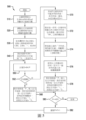
顯示驅動器210的基本的驅動流程300的流程圖在圖3中示出。依據第一步驟310,顯示驅動器210從記憶體202下載(箭頭290)事件表及數據查表(例如,位元平面序列表600)。依據第二步驟320,顯示驅動器210將非預設顯示設定經成像指令連接250寫入顯示器220。依據第三步驟330,顯示驅動器210等待來自標記影片幀開始的影片源(未示出)的同步標記(Synchronization Marker,Vsync)332。在接收到同步標記(Vsync)332後,依據第四步驟340,顯示驅動器210依據下載的表執行一系列事件。
A flowchart of a
特別地,第四步驟340包含在第一子步驟342初始化幀計時器及加載第一事件時間,在第二子步驟344等待事件時間,在第三子步驟346執行位元平面(發送到顯示器220的LCOS)或其他事件,依據第四子步驟348判斷事件是否為最後一個事件。若事件非最後一個事件,依據子步驟350加載一新事件時間並重複子步驟344、346、348、350直到在子步驟348事件被判斷為最後一個事件。
Specifically, the
顯示流程show process
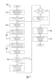
圖4示出了顯示器220上的渲染(Rendering)過程400的基本流程圖。當於步驟410處於空閒狀態時,顯示器220從顯示驅動器210經成像影片數據連接240接收影像數據。依據第一步驟412,顯示器220通過平行介面解析接收的影像數據以判斷是否接收到有效的LCOS標頭(Header)。若於步驟414沒有幀計時器被更新,顯示器220回到步驟410空閒狀態。若有,則於步驟416將標頭儲存到顯示器220內的內部暫存器,且顯示器220接著於步驟420過渡到位元平面接收狀態。
FIG. 4 shows a basic flowchart of a rendering (Rendering)
顯示器220由平行介面接收128行位元並於步驟422儲存
到合適的像素的主正反器(Flip-Flop)。在接收之後隨後於步驟424遞增行選擇計數器,重複步驟422及424直到於步驟426判斷接收到所有行數據。在行接收完成之後,於步驟430遞增列選擇計數器且在接收下一個列的第一行數據之前歸零行選擇計數器。重複上述步驟直到於步驟432判斷最後一列和最後一行的數據都被接收,此時顯示器220於步驟440過渡到負載狀態。
當於步驟440處於負載狀態時,顯示器220於步驟450發送負載脈衝以將整個行組的主正反器數據移動到附屬正反器,接著於步驟452延遲預定數量的循環,然後於步驟454遞增行選擇計數器並在所有剩餘的行組重複。在步驟456判斷對所有行組重複此過程後,於步驟460發送位準偏移觸發器以同時更新所有的附屬正反器數據到電極,並且顯示器220於步驟410回到空閒狀態。
While in the load state at
位元平面表方法Bit Plane Table Method
當由顯示驅動器210發送到相位模式位元平面驅動的數位LCOS顯示器220時,這裡所述的系統和方法判斷優化「1」和「0」的位元平面(例如,參見圖6的位元平面序列表600)的序列,導致波形100處於具有最小相位波紋110的期望的相移值120。
The systems and methods described herein determine which bit-planes optimize "1"s and "0's" when sent by the
相位模式與振幅模式Phase Mode vs. Amplitude Mode
對於上下文,簡要描述了在相位與振幅模式下操作數位LCOS顯示器220之間的差異。通常。在振幅模式中,顯示系統200以PWM操作。於此,對於要在特定灰階等級顯示的給定的幀中的給定像素,在幀開始的時後像素被導通,並以值「1」重寫,使其在每一位元平面導通直到達到對應於所需的「全刻度(Full-Scale)」的百分比的時間點。
For context, the differences between operating the
因此,例如,灰階值為「0」時,像素永遠不會被導通。灰階值為50%時,像素通常在幀的前半部維持導通,並在下半部維持關斷。灰階值為100%時,像素近乎在整個幀都維持導通。因此,通常,每一個 像素在每個位元平面寫入一長串值「1」直到某個時間點,接著從該時間點寫入一長串值「0」直到幀結束。 So, for example, when the grayscale value is "0", the pixel will never be turned on. At a grayscale value of 50%, the pixel typically remains on for the first half of the frame and remains off for the second half. When the grayscale value is 100%, the pixel remains on for almost the entire frame. Therefore, usually, each A pixel writes a long string of "1" values in each bit-plane until a certain point in time, and then writes a long string of "0" values from that point in time until the end of the frame.
各種灰階值的結果在圖10中示出。對於這些振幅模式情況,僅存在對應於可能灰階等級(22)的示例數量的4個位元平面寫入。Vsync脈衝在每幀的關斷開始,接著是像素電壓波形及對應的LC響應。在圖表上,有四個虛線框;每個為一個可能的灰階值,其可代表需要四個不同灰階等級的四個不同像素的電壓及LC響應。在60HZ,整個序列需要16.67ms完成,並且會在下一幀中重複(但極性相反以獲得直流平衡)。 The results for various grayscale values are shown in FIG. 10 . For these amplitude mode cases, there are only 4 bit-plane writes corresponding to an example number of possible gray scale levels (2 2 ). The Vsync pulse starts at the turn-off of each frame, followed by the pixel voltage waveform and corresponding LC response. On the graph, there are four dashed boxes; each is a possible gray scale value, which can represent the voltage and LC response of four different pixels requiring four different gray scale levels. At 60HZ, the entire sequence takes 16.67ms to complete and is repeated in the next frame (but with reversed polarity for DC balance).
於此,應該理解的是(除了少部份的接近0的灰階值),顯示器220的液晶222總是有時間在PWM脈衝結束之前達到完全導通狀態,並且(除了接近全刻度的幾個灰階值)在此後達到完全關斷的狀態。
Here, it should be understood that (except for a small number of gray scale values close to 0), the
就位元平面時機而言(這受所期望的伽瑪影響,但與其無關),位元平面的平均間隔大約為幀時間除以可能的灰階等級的數量。這個數量通常比最小可能的位元平面時間長得多,並且根據所需的伽瑪值,得到的幀時間越長,這個間隔越大。 In terms of bit-plane timing (which is affected by, but not related to, the desired gamma), the average spacing of bit-planes is approximately the frame time divided by the number of possible gray levels. This amount is usually much longer than the smallest possible bit-plane time, and depending on the desired gamma value, the longer the resulting frame time, the larger this interval will be.
顯示系統200在相位模式下的操作是不同的。於此,顯示系統200被設計成使得顯示器220的液晶222不會達到「完全導通」或「完全關斷」狀態。相反的,顯示驅動器210發送1和0的模式,使得液晶222的狀態以鋸齒形方式來回移動,使其保持在對應於期望的相移值120的「完全導通」的期望的百分比。
The operation of
各種相位值的結果示出於圖11中。於此,存在有16個位元平面寫入,並且可以理解的是,只要像素電壓需要改變,就存在位元平面寫入。在位元平面寫入之間的60us處,此圖僅描述了幀的前960us或小於幀的1/16。虛線大致示出了液晶狀態平均,其旨在為期望的相移。 The results for various phase values are shown in FIG. 11 . Here, there are 16 bit-plane writes, and it is understood that there are bit-plane writes whenever the pixel voltage needs to be changed. At 60us between bitplane writes, this graph only depicts the first 960us of a frame or less than 1/16 of a frame. The dashed line roughly shows the liquid crystal state average, which is intended for the desired phase shift.
每當發送值「1」位元平面時,液晶狀態開始傾向「完全導通」,並且每當發送值「0」位元平面時,液晶狀態開始傾向「完全關斷」。
液晶狀態總是傾向一個方向或另一個方向。發生這些位元平面發送的時間越遠,在一個方向上的傾斜時間越長,因此相位波紋110或波形100的鋸齒波的振幅越大。
Whenever a bit-plane of value "1" is sent, the liquid crystal state begins to lean towards "full on", and whenever a bit-plane of value "0" is sent, the liquid crystal state begins to lean towards "full off".
The liquid crystal state always favors one direction or the other. The further back in time these bit plane transmissions occur, the longer the tilt in one direction, and thus the greater the amplitude of the
顯示系統200將位元平面610非常靠近地寫入,以便最小化相位波紋110。位元平面610寫入之間的最短間隔可能是有限的例如大約為60us。
根據溫度,相位模式液晶222的當前材料的上升和下降時間可以是例如3ms左右。在這種情況下,即使相同模式的位元平面610的相當長的序列(例如,一系列的1或一系列的0)也不一定會使液晶狀態進入飽和狀態(「完全導通」或「完全關斷」)。
Depending on the temperature, the rise and fall times of the current material of the phase
作為示例,為了獲得60%的「完全導通」的液晶狀態,具有60%的「1」及40%的「0」的「1」位元平面610和「0」位元平面610的模式可能會達到預期的效果。然而,序列620的特定模式是重要的,以便最小化相移值120周圍的相位波紋110。
As an example, to obtain a 60% "fully on" liquid crystal state, a pattern of "1"
所選擇的序列620的模式應用正確的占空比以便獲得改進的相移值120並且最小化系統在一列中發送一些「導通」或「關斷」位元平面的時間(因為這傾向於如上關於圖1所述,增加相位波紋110)。現在將更詳細地描述用於判斷實現這兩個目標的最佳模式600的方法500。
The selected pattern of
位元平面表產生方法Bit Plane Table Generation Method
通常,二進位值序列在幀或子幀期間達到期望的灰階或相位值,並且通過在該幀或子幀中與「關斷」值散佈用於該灰階或相位值的期望的「導通」值的數量,使得「導通」時段在幀或子幀期間內基本上等間隔地發生。 Typically, a sequence of binary values reaches a desired grayscale or phase value during a frame or subframe, and the desired "on" for that grayscale or phase value is achieved by interspersing with an "off" value in that frame or subframe. ” values such that the “on” periods occur at substantially equal intervals within a frame or subframe period.
我們將每個幀或子幀分割為b=m×(2n-1)個這樣的導通或關斷值,其中n是幀或子幀的整數本體位元深度,而m是選擇的整數乘數,使得b位元平面負載可以在幀或子幀期間基本上均勻地間隔地發生,而不 需要以比LCOS及其驅動電路可以實現的更高的速率以發生位元平面負載。 We divide each frame or subframe into b = m × (2 n -1) such on or off values, where n is the integer body bit depth of the frame or subframe and m is a chosen integer times number such that b-bit-plane loads can occur substantially evenly spaced during a frame or sub-frame without requiring bit-plane loads to occur at a higher rate than the LCOS and its driver circuitry can achieve.
方法500根據每個序列620中可能的相移值(表600的行)判斷表600的模式在時間間隔中將存在多少「導通」或「1」位元平面610(表600的列),並且在該時間間隔的時段內盡可能相等地散佈「導通」或「1」位元平面610。剩餘的位元平面時間將是「關斷」或「0」位元平面610。方法500於以下描述並在圖5中示出。
The
例如,對於6位元相位模式顯示器220,系統和方法500判斷應用於64個由6位元相移解析度定義的可能相移值120中的每一個的優化序列620(在表600中由列代表的相移值(序列620)的可能性,由表600中的行指示的位元平面610;每一列是用於相移值的位元平面的序列)。
For example, for a 6-bit phase-
方法500包含判斷幀時間及相移解析度的位元數量的第一步驟510。例如,60Hz幀具有16.667ms時段的幀時間。各種相移解析度被考量。作為示例,如果選擇6位元的相移解析度,則在基本調變序列中存在64(26)位元的相移解析度,並且判定模式以支持從64中有0到64中有63為「1」序列620的可能性。
繼續該示例,最小調變時間是64*60us=3.84ms。根據第二步驟520,判斷64位元平面序列(調變時間)在幀內重複的次數。於此,幀時間是16.667ms長,因此有重複這64位元平面序列4.34次的時間。
Continuing with the example, the minimum modulation time is 64*60us=3.84ms. According to a
接著調整每一位元平面610的時間使得重複的次數為整數。例如,位元平面610的時間被調整到65.1us以在幀時間內具有正好四次64位元平面序列(調變模式)的重複。
The time of each bit-
方法500繼續一系列的子步驟,用於為64個可能的相移值中的每一個選擇(位元模式)序列620。
依據第三步驟530,相移值被正規化且從本體的0-2π相移值120捨入到0/64、1/64、2/64、3/64、...、63/64。在每種情況下,分子
(P)是64個中可能的「導通」或「1」位元平面的數量。應當理解的是,如果需要,可以經乘以2π將這些分數中的每一個轉換回相移值(以弧度表示)。
According to a
依據第四步驟540,對於0的相移,所有的64位元平面為「0」。P被設定為從值1開始。
According to the
依據第五步驟550,「導通」位元平面的平均間隔(D)通過將64除以分子值(P)來判斷。例如,對於對應到8/64(0.785弧度)的相移,64被除以8以得到結果8.0。這表示每一個第8位元平面會需要是「導通」位元平面。
According to the
依據第五步驟550的子步驟552,對於每一個D值及關聯的P值,判斷D是否為整數。
According to
依據第六步驟560,對於出現均勻的除法的相移值(D產生整數結果),判斷序列620的模式。在序列620的模式中,「導通」或「1」位元平面為0(第一)、8、16、24、32、40、48和56。對於2π的相移(全刻度),所有64位元平面都是「1」。對於1π(中間刻度)的相移,模式在1和0交替(各32)為「10101010...」。
According to a
然而,對於大多數的相移值(與分子P相關聯),步驟550的除法在步驟552不會產生整數結果。例如,對應於3/64(弧度0.295)的相移,除法結果是64/3=21.3。這將對應於每21.3位元平面的「導通」位元平面。然而,「導通」位元平面不能在表600中有小數或非整數位置。相反地,根據一系列子步驟570、572、574、576、578,三個「導通」位元平面的非小數位置被判定為盡可能的均勻,使得「導通」位元平面610之間的平均間隔盡可能接近21.3。
However, for most values of the phase shift (associated with the numerator P), the division of
通常,對於每個非整數間隔,系統列舉最接近期望間隔的模式,計算每個模式的平均間隔,並且消除除了具有最接近期望平均的平均間隔的模式之外的所有圖案。如果存在超過一個具有相同的最接近平均間間隔模式(如上例所示),則系統選擇在位元平面上具有最早「額外」的模 式。 Typically, for each non-integer interval, the system enumerates the patterns closest to the desired interval, calculates the average interval for each pattern, and eliminates all but the pattern with the average interval closest to the desired average. If there is more than one pattern with the same closest mean interval (as in the example above), the system chooses the pattern with the earliest "extra" on the bit plane. Mode.
於此,依據子步驟570,對於每個非整數D值,系統判斷間隔為int(D)或int(D)+1。對於上面的例子,間隔將分別為21或22(int(21.3)或int(21.3)+1)。
Here, according to
依據子步驟570,系統另外形成所有可能序列的列表(與分子P相關聯)。作為示例,如果每個重複從具有「導通」位元平面的0開始,則繼續上述示例的選擇是{0,21,42},{0,21,43},{0,22,43},或{0,22,44}。 According to sub-step 570, the system additionally forms a list of all possible sequences (associated with molecule P). As an example, if each repetition starts with a 0 with an "on" bit-plane, the choices to continue the above example are {0,21,42}, {0,21,43}, {0,22,43}, or {0,22,44}.
依據子步驟572,對於每一序列,系統計算相鄰元件之間的平均差。這包含了最後一個元件和「64」之間的「概括(Wrap-Around)」差。對於示例的序列,每個序列的平均間隔分別為:21.3,21.3,21.3和21.7。 According to sub-step 572, for each sequence, the system calculates the average difference between adjacent elements. This includes the "Wrap-Around" difference between the last element and "64". For the example sequences, the mean intervals for each sequence are: 21.3, 21.3, 21.3, and 21.7.
依據子步驟574,系統將每個平均間隔與D的值進行比較,並確定哪個或哪些序列關聯於最小差。繼續上面的例子,在計算的平均間隔中,最後一個被消除,因為該平均間隔離目標21.3最遠。選項{0,21,42},{0,21,43}和{0,22,43}仍然存在且其中任何一個都是有效的選擇。 Pursuant to sub-step 574, the system compares each average interval to the value of D and determines which sequence or sequences are associated with the smallest difference. Continuing with the example above, the last one is eliminated in the average interval calculated because it isolates the target 21.3 furthest. The options {0,21,42}, {0,21,43} and {0,22,43} still exist and any of them are valid choices.
依據子步驟576,系統使用所判定的序列或從剩餘序列中進行選擇。例如,從剩餘的示例序列中進行選擇,選擇第二個選擇{0,21,42},因為它在幀中較早放置一個「導通」位元平面,其將加速以提前一點達到所需相位值的過程。 According to sub-step 576, the system uses the determined sequence or chooses from the remaining sequences. For example, choosing from the remaining example sequences, the second choice {0,21,42} is chosen because it places an "on" bit plane early in the frame, which will speed up to reach the desired phase a bit earlier value process.
依據子步驟578,在每一個相移值(P),在位元平面序列表600依據所選的序列填入位元平面值。該序列表示對於給定的P值具有「導通」值的位元平面610。
According to sub-step 578, at each phase shift value (P), the bit-plane sequence table 600 is populated with bit-plane values according to the selected sequence. The sequence represents bit-
依據子步驟580、582,重複方法500的步驟以得額外的值。
According to
圖6示出了繪示在上述的示例性的64位元系統中,對於每一個可能的64相移等級的位元平面會是「導通」的示例的圖。需注意每一列為不同的相移;灰色或黑色單元為「導通」位元平面。 FIG. 6 shows a diagram illustrating examples of how a bit plane would be "on" for each of the possible 64 phase shift levels in the exemplary 64-bit system described above. Note that each column is a different phase shift; gray or black cells are "on" bit planes.
旋轉循環spin cycle
如上所述,每一幀或子幀被分b=m×(2n-1)的「導通」或「關斷」值,其中n為幀或子幀的負整數本體位元深度,而m是選擇的整數乘數,使得b位元平面負載可以在幀或子幀期間基本上均勻地間隔地發生,而不需要以比LCOS及其驅動電路可以實現的更高的速率以發生位元平面負載。 As described above, each frame or subframe is assigned an "on" or "off" value of b=m×(2n-1), where n is the negative integer bit depth of the frame or subframe, and m is An integer multiplier chosen such that b-bit-plane loads can occur substantially evenly spaced during a frame or sub-frame without requiring bit-plane loads to occur at a higher rate than LCOS and its driver circuitry can achieve .
對於每一所需的灰階或相位值,系統循環地以整數值旋轉b「導通」或「關斷」值的序列。例如,系統選擇一組的整數旋轉值,每個相位或灰階值一組,其共同導致b位元平面負載中的每一個的大致相同數量的導通到關斷轉換以及大致相同數量的關斷到導通轉換。因此,導通到關斷轉換的速率以及關斷到導通轉換的速率在幀或子幀內維持大致恆定。 For each desired grayscale or phase value, the system cyclically rotates the sequence of b "on" or "off" values by integer values. For example, the system selects a set of integer rotation values, one set for each phase or grayscale value, which together result in approximately the same number of on-to-off transitions and approximately the same number of off transitions for each of the b-bit planar loads to conduction transition. Thus, the rate of on-to-off transitions and off-to-on transitions remains approximately constant within a frame or sub-frame.
作為另一示例,系統從一組可能的獨特旋轉值(b個旋轉值中僅m=2n×b個獨特選擇,導致b個導通和關斷值的不同序列)中選擇一組整數旋轉值。此選擇是由數值地評估一些或所有m個可能的集合來判斷,以最小化或最大化一或多個數值定義的優點函數(Merit Function)。 As another example, the system selects a set of integer rotation values from a set of possible unique rotation values (only m = 2nxb unique choices of b rotation values, resulting in a different sequence of b on and off values). The selection is determined by numerically evaluating some or all of the m possible sets to minimize or maximize one or more numerically defined Merit Functions.
例如,可以相對於導通到關斷轉換的時間分佈的均勻性來判斷該選擇。或者,可以判斷該選擇以防止在幀或子幀中的某些時刻發生大量的關斷到導通轉換,例如,在幀或子幀的開始或結束。 For example, the choice can be judged with respect to the uniformity of the time distribution of the on-to-off transitions. Alternatively, the selection may be judged to prevent a large number of off-to-on transitions at certain times in a frame or subframe, eg, at the beginning or end of a frame or subframe.
或者,可以藉由一次一個地量測一或多個具有一些或全部m個可能組合的LCOS的優點函數,來實驗性地判斷該選擇。於此,量測的優點函數可以例如是以該組旋轉值操作的LCoS的繞射效率。作為另一示例,優點函數可以是在由該組旋轉值操作的LCoS產生的一階繞射圖像的第一基本亮區中測量的光功率,與在由該組旋轉值操作的LCoS產生的一階繞射圖像的第二基本上測量的光功率之間的比例;或是在一階繞射圖像的共軛的空間對應區域中測量。 Alternatively, the choice can be determined experimentally by measuring the merit function of one or more LCOSs with some or all of the m possible combinations one at a time. Here, the measured merit function may eg be the diffraction efficiency of the LCoS operating on the set of rotation values. As another example, the merit function may be the difference between the optical power measured in the first elementary bright region of the first-order diffraction image produced by the LCoS operated by the set of rotation values compared to the optical power produced by the LCoS operated by the set of rotation values The ratio between the second substantially measured optical powers of the first order diffraction image; or measured in a conjugate spatially corresponding region of the first order diffraction image.
另外,可以通過混合方法來判斷選擇,其中候選的組合是從 可能的組合中數字地選出,且接著實驗性地評估這些候選的組合。 Alternatively, selection can be judged by a hybrid approach, where combinations of candidates are selected from Possible combinations are numerically selected, and then these candidate combinations are evaluated experimentally.
實務上,每個位元平面同時設定顯示器內的每個像素,且幾百萬個基本上同時轉換的像素可以導致系統等級的交互。若位元序列被認為如圖6中所示,在一個位元平面和下一個位元平面之間的像素改變狀態(從0到1或從1到0)的相移值的數量可以少至20或者多達41個。隨著被應用於包含幾百萬個像素的成像器廣泛範圍的相移值的影像,當在幀的過程中執行的位元平面時,各種的活動等級(Activity Level)產生可見的假影(Artifacts)。 In practice, each bit-plane simultaneously sets every pixel in the display, and millions of pixels switching substantially simultaneously can result in system-level interactions. If the sequence of bits is considered as shown in Figure 6, the number of phase shift values for a pixel to change state (from 0 to 1 or from 1 to 0) between one bit-plane and the next can be as little as 20 or as many as 41. With images of a wide range of phase shift values applied to imagers containing millions of pixels, various Activity Levels produce visible artifacts ( Artifacts).
在框架的過程中的一系列像素1和0狀態經其混合和分散的1和0達到目標相移。它們不依賴於在序列的任何特定點開始1和0的序列。因此,系統執行計算在每一位元平面之間像素狀態改變的數量的優化步驟並調整與每個目標相位狀態值關聯的每個1和0的系列的起始點,以最小化在連續位元平面之間的計算的像素狀態改變的最小數量,與在連續位元平面之間的計算的像素狀態改變的最大數量之間的範圍。應用此優化可以大幅地減少假影並提高相位對比度。
A series of
每位元平面可變電壓Plane variable voltage per bit
圖8是示例性基準位元平面序列表800,而圖9是修改的位元平面序列表900(經將以上及/或以下的優化應用到圖8示出的位元平面序列表800的基準設定而產生的位元平面集合)。為了達到示範的目的,以下稱位元平面序列表800為基準位平面序列表800,方法700的說明將於以下描述。
FIG. 8 is an exemplary reference bit-plane sequence table 800, while FIG. 9 is a modified bit-plane sequence table 900 (baseline by applying the above and/or following optimizations to the bit-plane sequence table 800 shown in FIG. A set of bit-planes generated by setting). For demonstration purposes, the bit-plane sequence table 800 is referred to as the reference bit-plane sequence table 800 hereinafter, and the description of the
再次參考圖2,顯示系統200的微代碼驅動器架構可以獨立於其他位元平面改變發送到顯示器220的位元平面的細節。這些細節之一是施加到給定位元平面的像素電極的電壓。此電壓(Vpix電壓270)在此示例性實施例中從外部混合訊號晶片230提供給顯示器220,其中實際電壓由從顯示驅動器210以SPI介面寫入經成像器指令連接250到混合訊號晶
片230來設定。
Referring again to FIG. 2 , the microcode driver architecture of
初始化該\經成像器指令連接250的SPI介面寫入,並且寫入的值由已插入或呈現到下載的事件表中的命令判定。因此,藉由下載新的事件表,可以對用於每一位元平面的Vpix電壓270進行單獨的調整。
The \ is initialized for writing via the SPI interface of the
依據電壓調整方法700,連續地對每一位元平面進行小的實驗電壓調整,通常從發送的第一位元平面開始,並且在每一調整後進行相位波紋110量測。
According to the
例如,供予幀(或序列/列)中的一或兩個位元平面且通常僅為0.1或0.2V的小電壓調整,對於降低相位波紋110的平均數量可以非常有效。特別的是,特別對幀中的第一個位元平面或最後一個位元平面(或兩者)進行這些電壓調整是最有效的。
For example, a small voltage adjustment, typically only 0.1 or 0.2V, for one or two bit-planes in a frame (or sequence/column) can be very effective in reducing the average amount of
此效果最容易理解為部分地「校正」或「補償」由在幀的期間出現的位平面序列之前和之後的不活動時段所引起的不對稱性。這些調整應該以在持續運作的過程中仍然為顯示器220保持整體的直流平衡的方式進行,因為LCOS顯示器220上存在的任何殘餘的直流電壓可以導致閃爍及影像殘留假影。
This effect is most easily understood as "correcting" or "compensating" in part the asymmetry caused by periods of inactivity before and after the sequence of bit-planes occurring during the frame. These adjustments should be made in a manner that still maintains an overall DC balance for the
參考圖7,現在更詳細地描述示利性的電壓調整方法700。依據第一步驟710,基準位元平面序列表800被下載到顯示驅動器210。位元平面序列表800將位元平面Vpix電壓270設定到基準值。
Referring to FIG. 7 , an exemplary
依據第二步驟720,顯示系統200使用此基準位元平面序列表800量測相位波紋110並將結果儲存為此位元平面的基準(#0)。
According to the
依據第三步驟730,顯示系統200修改基準位元平面序列表800以僅對第一位平面施加+100mV的Vpix偏移(相對於「基準」值)。修改的相位模式序列表被下載到顯示驅動器210,顯示系統200使用此新的序列量測相位波紋110並且將結果儲存為(#1)。
According to a
依據第四步驟740,顯示系統200修改基準位元平面序列表
800以僅對第一位平面施加-100mV的Vpix偏移(相對於「基準」值)。修改的相位模式序列表被下載到顯示驅動器210,顯示系統200使用此新的序列量測相位波紋110並且將結果儲存為(#2)。
According to the
依據第五步驟750,顯示系統200將結果#0的相位波紋110與結果#1和#2的相位波紋110做比較。若#1或#2有低於#0的相位波紋,將基準序列中此第一位元平面的基準Vpix電壓270取代為修改的產生較小相位波紋110的Vpix電壓(Vpix電壓270及Vpix偏移)。
According to the
對於序列中的每個位元平面重複步驟710、720、730、740、750。在每種情況下,如果發現特定位元平面的Vpix電壓270的電壓偏移給出比先前的「低」相位紋波110值更低的相位紋波110值,則Vpix電壓270值被替換該位元平面的基準序列中具有導致較低的整體相位波紋110的值。接著將新的「修改的序列」用於剩餘的步驟。
此些值可以交互作用,因此對於序列620中的每個位元平面610重複多於一次的步驟可能是有利的。重複具有小於100mV的電壓偏移的演算法以微調最終的結果也可能是有利的。考量其他偏移。
Such values may interact, so it may be advantageous to repeat the steps more than once for each bit-
依據第六步驟760,顯示系統200對相反極性的子幀進行改變,在組合的正和負子幀上重新檢查相位波紋110。對正和負子幀的改變具有相同的幅度和相反的極性,以確保維持直流平衡。在這些組合的子幀上重複流程700以進一步最小化相位波紋110可能是有利的。
According to a
依據第七步驟770,顯示系統200保存並儲存合併Vpix偏移的最終修改的「基準」序列900、1000。
According to a
流程700是驅動序列及液晶構成的工程優化的一部份。
結論in conclusion
類比設計在歷史上一直受到青睞,因為數位設計一直被認為不能產生全像術(Holography)所需的準確的低相位波紋的相移。然而,數位相位模式LCOS顯示器在許多方面可以說至少具有競爭力,且通常優於 類比設計。數位相位模式LCOS顯示器具有與類比版本相媲美的相位紋波-對於6位元解析度通常為3%或更低。數位相位模式LCOS顯示器有更少的或甚至沒有「衰減(Droop)」和不準確電荷移轉中的每一個,其為類比顯示器具有的問題一尤其是對於更小尺寸的像素。因為數位相位模式LCOS顯示器不需要最小尺寸以切合每一像素中的儲存電容器,因此它們能夠以更小的像素實現。例如,數位相位模式LCOS顯示器可以使用3.015um的像素間距,且可以使用更小的像素。沒有類比相位模式顯示器展示這麼小的像素。 Analog designs have historically been favored because digital designs have been considered incapable of producing the accurate, low-ripple phase shift required for holography. However, digital phase mode LCOS displays are in many respects arguably at least competitive, and often superior to Analogy design. Digital phase mode LCOS displays have phase ripple comparable to analog versions - typically 3% or less for 6-bit resolution. Digital phase mode LCOS displays have less or even no each of the "Droop" and inaccurate charge transfer that is a problem with analog displays—especially for smaller sized pixels. Since digital phase mode LCOS displays do not require a minimum size to fit the storage capacitor in each pixel, they can be implemented with smaller pixels. For example, a digital phase mode LCOS display can use a pixel pitch of 3.015um, and can use smaller pixels. No analog phase mode display exhibits such small pixels.
數位結構提供更加改善的對雜訊、偏移電壓、接地彈跳、電源電壓抑制比(Power Supply Rejection Ratio,PSRR)問題及造成類比LCOS顯示器的設計更有難度的其他假影的抗擾度。 The digital architecture provides improved immunity to noise, offset voltage, ground bounce, Power Supply Rejection Ratio (PSRR) issues, and other artifacts that make designing for analog LCOS displays more difficult.
該系統及方法允許顯示比現有顯示器產生的相位影像具有更高的對比度的相位影像。藉由提供一種以降低的相位波紋操作顯示器的方法,改善了對比度。這使得使用於此所述的系統及方法創造的顯示器更好(因為它們產生更高質量的影像)且更適合終端客戶使用。 The systems and methods allow the display of phase images with higher contrast than those produced by existing displays. Contrast is improved by providing a method of operating a display with reduced phase ripple. This makes displays created using the systems and methods described herein better (because they produce higher quality images) and more suitable for end-customer use.
這裡使用的術語和表達是作為描述的術語而非限制,並且在使用這些術語和表達時,無意排除所示和所述特徵的任何等同物(或其部份),且可以認知到,在申請專利範圍內可以進行各種修改。因此,申請專利範圍旨在涵蓋所有這些等同物。 The terms and expressions used herein are terms of description rather than limitation, and in using these terms and expressions, there is no intention to exclude any equivalents (or parts thereof) of the features shown and described, and it will be recognized that in the application Various modifications are possible within the scope of the patent. Accordingly, the scope of the patent application is intended to cover all such equivalents.
本文已描述各種特徵、方面和實施例。如本領域之具有通常知識者可理解的,本公開的特徵、方面和實施例易於彼此組合以及變化和修改。因此,本公開應被視為包含這些組合、變化和修改。 Various features, aspects and embodiments have been described herein. The features, aspects and embodiments of the present disclosure are easily combined with each other as well as changes and modifications as can be understood by those having ordinary knowledge in the art. Therefore, the present disclosure should be construed as including such combinations, changes and modifications.
雖然本發明以前述之實施例揭露如上,然其並非用以限定本發明。在不脫離本發明之精神和範圍內,所為之更動與潤飾,均屬本發明之專利保護範圍。關於本發明所界定之保護範圍請參考所附之申請專利範圍。 Although the present invention is disclosed by the aforementioned embodiments, they are not intended to limit the present invention. Without departing from the spirit and scope of the present invention, all changes and modifications are within the scope of patent protection of the present invention. For the scope of protection defined by the present invention, please refer to the appended scope of patent application.
100:典型波形 100: typical waveform
110:相位波紋 110: Phase ripple
120:相移值 120: Phase shift value
200:顯示系統 200: display system
202:記憶體 202: memory
210:顯示驅動器 210: display driver
220:顯示器 220: Display
222:液晶 222:LCD
230:混合訊號晶片 230: mixed signal chip
240:成像影片數據連接 240: Imaging film data connection
250:成像指令連接 250: Imaging instruction connection
260:連接 260: connect
270:Vpix輸出電壓 270: Vpix output voltage
280:Vcom輸出電壓 280: Vcom output voltage
290:箭頭 290: arrow
600:位元平面序列表 600: bit plane sequence table
610:位元平面 610: bit plane
620:序列 620: sequence
800:位元平面序列表 800: bit-plane sequence table
900、1000:修改的位元平面序列表 900, 1000: Modified bit-plane sequence list
圖1係包含先前技術的相位波紋的波形的圖解說明。 圖2係依據本發明的實施例的包含顯示驅動器及顯示器的顯示系統的示意圖。 圖3係依據本發明的圖2的顯示驅動器所繪示的示例性驅動器過程的流程圖。 圖4係依據本發明的圖2的顯示器所繪示的示例性顯示過程的流程圖。 圖5係依據本發明的用於產生位元平面序列表的示例性位元平面產生流程的流程圖。 圖6係依據本發明的根據圖5的位元平面序列流程所產生的示例性位元平面序列表的圖解說明。FIG. 1 is a graphical illustration of a waveform containing prior art phase ripple. FIG. 2 is a schematic diagram of a display system including a display driver and a display according to an embodiment of the invention. 3 is a flowchart of an exemplary driver process depicted by the display driver of FIG. 2 in accordance with the present invention. FIG. 4 is a flowchart of an exemplary display process depicted by the display of FIG. 2 according to the present invention. 5 is a flowchart of an exemplary bit-plane generation process for generating a bit-plane sequence table in accordance with the present invention. FIG. 6 is a diagram illustrating an exemplary bit-plane sequence table generated according to the bit-plane sequence flow of FIG. 5 in accordance with the present invention.
圖7係依據本發明所繪示的示例性位元平面電壓調整方法的流程圖。 FIG. 7 is a flow chart of an exemplary bit-plane voltage adjustment method according to the present invention.
圖8係依據本發明所繪示的示例性基準位元平面序列表的圖解說明。 FIG. 8 is a diagram illustrating an exemplary reference bit-plane sequence table shown in accordance with the present invention.
圖9係示例性修改的位元平面序列表的圖解說明。 Figure 9 is a diagrammatic illustration of an exemplary modified bit-plane sequence table.
圖10係示例性振幅模式的圖解說明。 Figure 10 is a graphical illustration of an exemplary amplitude pattern.
圖11係示例性相位模式的圖解說明。 Figure 11 is a graphical illustration of an exemplary phase pattern.
200‧‧‧顯示系統 200‧‧‧display system
202‧‧‧記憶體 202‧‧‧memory
210‧‧‧顯示驅動器 210‧‧‧display driver
220‧‧‧顯示器 220‧‧‧display
222‧‧‧液晶 222‧‧‧LCD
230‧‧‧混合訊號晶片 230‧‧‧mixed signal chip
240‧‧‧成像影片數據連接 240‧‧‧imaging video data connection
250‧‧‧成像指令連接 250‧‧‧imaging instruction connection
260:連接 260: connect
270:Vpix輸出電壓 270: Vpix output voltage
280:Vcom輸出電壓 280: Vcom output voltage
290:箭頭 290: arrow
600:位元平面序列表 600: bit plane sequence table
Claims (19)
Applications Claiming Priority (2)
| Application Number | Priority Date | Filing Date | Title |
|---|---|---|---|
| US201862676148P | 2018-05-24 | 2018-05-24 | |
| US62/676,148 | 2018-05-24 |
Publications (2)
| Publication Number | Publication Date |
|---|---|
| TW202004717A TW202004717A (en) | 2020-01-16 |
| TWI794499B true TWI794499B (en) | 2023-03-01 |
Family
ID=66858026
Family Applications (1)
| Application Number | Title | Priority Date | Filing Date |
|---|---|---|---|
| TW108118029A TWI794499B (en) | 2018-05-24 | 2019-05-24 | Systems and methods for improving operating characteristics of displays |
Country Status (8)
| Country | Link |
|---|---|
| US (4) | US11455975B2 (en) |
| EP (1) | EP3803839A1 (en) |
| JP (3) | JP2021525387A (en) |
| KR (4) | KR20250172890A (en) |
| CN (2) | CN118506749A (en) |
| MY (1) | MY201285A (en) |
| TW (1) | TWI794499B (en) |
| WO (1) | WO2019227047A1 (en) |
Families Citing this family (4)
| Publication number | Priority date | Publication date | Assignee | Title |
|---|---|---|---|---|
| KR20250172890A (en) | 2018-05-24 | 2025-12-09 | 스냅 인코포레이티드 | Systems and methods for improving operating characteristics of displays |
| KR102216093B1 (en) * | 2019-05-08 | 2021-02-16 | 박상훈 | Letter block set for education |
| KR20250049453A (en) | 2020-12-10 | 2025-04-11 | 스냅 인코포레이티드 | Dual-voltage pixel circuitry for liquid crystal display |
| TWI888449B (en) * | 2020-12-15 | 2025-07-01 | 美商思娜公司 | Pixel circuitry, display including the same, and method for operating the same |
Citations (4)
| Publication number | Priority date | Publication date | Assignee | Title |
|---|---|---|---|---|
| US5185602A (en) * | 1989-04-10 | 1993-02-09 | Cirrus Logic, Inc. | Method and apparatus for producing perception of high quality grayscale shading on digitally commanded displays |
| US20120069060A1 (en) * | 2007-01-04 | 2012-03-22 | Micron Technology, Inc. | Nor-based grayscale for a digital display |
| US20150009203A1 (en) * | 2012-03-22 | 2015-01-08 | Bae Systems Plc | Generation and display of digital images |
| TW201532018A (en) * | 2014-01-03 | 2015-08-16 | 皮克斯特隆尼斯有限公司 | Artifact mitigation for composite primary color transition |
Family Cites Families (16)
| Publication number | Priority date | Publication date | Assignee | Title |
|---|---|---|---|---|
| EP0855693A1 (en) * | 1997-01-24 | 1998-07-29 | Digital Equipment Corporation | System and method for displaying blinking objects on a display device |
| KR20020006019A (en) * | 1998-12-14 | 2002-01-18 | 도날드 피. 게일 | Portable microdisplay system |
| GB9827944D0 (en) * | 1998-12-19 | 1999-02-10 | Secr Defence | Displays based on multiple digital bit planes |
| WO2001086619A1 (en) * | 2000-05-08 | 2001-11-15 | Philips Semiconductors, Inc. | A method and a system for color modulation |
| JP4017425B2 (en) | 2002-03-25 | 2007-12-05 | 川崎マイクロエレクトロニクス株式会社 | Simple matrix liquid crystal driving method and liquid crystal driving device |
| WO2005039167A2 (en) * | 2003-10-17 | 2005-04-28 | Leapfrog Enterprises, Inc. | Frame rate control systems and methods |
| DE102004025417B4 (en) * | 2004-05-24 | 2008-01-24 | Siemens Ag | Method for improving the image homogeneity of image data from phase-cycled steady-state sequences |
| BRPI0712687C8 (en) * | 2006-06-02 | 2019-09-10 | Compound Photonics Ltd | method for performing directed actions to transmit recording light; optical recording valve |
| JP2011043766A (en) * | 2009-08-24 | 2011-03-03 | Seiko Epson Corp | Conversion circuit, display drive circuit, electro-optical device, and electronic equipment |
| JP2011059610A (en) * | 2009-09-14 | 2011-03-24 | Seiko Epson Corp | Electro-optical device, driving method thereof, and electronic apparatus |
| JP2011064752A (en) * | 2009-09-15 | 2011-03-31 | Seiko Epson Corp | Electro-optical device, method for driving the same, and electronic equipment |
| US9591188B2 (en) * | 2013-08-01 | 2017-03-07 | Bass Roots Technologies, Llc | Cascaded bit sequences in display systems |
| JP2016024444A (en) * | 2014-07-24 | 2016-02-08 | 日本電信電話株式会社 | Pixel voltage generation method and optical signal processing apparatus |
| CN106205454A (en) * | 2016-07-06 | 2016-12-07 | 昀光微电子(上海)有限公司 | A kind of microdisplay on silicon module |
| EP3622502A1 (en) * | 2017-05-08 | 2020-03-18 | Compound Photonics Limited | Drive techniques for modulation devices |
| KR20250172890A (en) | 2018-05-24 | 2025-12-09 | 스냅 인코포레이티드 | Systems and methods for improving operating characteristics of displays |
-
2019
- 2019-05-24 KR KR1020257039029A patent/KR20250172890A/en active Pending
- 2019-05-24 KR KR1020247042598A patent/KR102890884B1/en active Active
- 2019-05-24 EP EP19730636.8A patent/EP3803839A1/en active Pending
- 2019-05-24 MY MYPI2020006161A patent/MY201285A/en unknown
- 2019-05-24 CN CN202410716386.XA patent/CN118506749A/en active Pending
- 2019-05-24 TW TW108118029A patent/TWI794499B/en active
- 2019-05-24 KR KR1020237013376A patent/KR102747508B1/en active Active
- 2019-05-24 CN CN201980034984.6A patent/CN112602146B/en active Active
- 2019-05-24 US US17/057,796 patent/US11455975B2/en active Active
- 2019-05-24 WO PCT/US2019/034004 patent/WO2019227047A1/en not_active Ceased
- 2019-05-24 KR KR1020207036708A patent/KR102527691B1/en active Active
- 2019-05-24 JP JP2020565472A patent/JP2021525387A/en active Pending
-
2022
- 2022-08-19 US US17/821,133 patent/US11893966B2/en active Active
- 2022-11-24 JP JP2022187458A patent/JP7534376B2/en active Active
-
2023
- 2023-12-05 US US18/529,566 patent/US12322360B2/en active Active
-
2024
- 2024-08-01 JP JP2024125776A patent/JP7820452B2/en active Active
-
2025
- 2025-04-23 US US19/187,684 patent/US20250299649A1/en active Pending
Patent Citations (4)
| Publication number | Priority date | Publication date | Assignee | Title |
|---|---|---|---|---|
| US5185602A (en) * | 1989-04-10 | 1993-02-09 | Cirrus Logic, Inc. | Method and apparatus for producing perception of high quality grayscale shading on digitally commanded displays |
| US20120069060A1 (en) * | 2007-01-04 | 2012-03-22 | Micron Technology, Inc. | Nor-based grayscale for a digital display |
| US20150009203A1 (en) * | 2012-03-22 | 2015-01-08 | Bae Systems Plc | Generation and display of digital images |
| TW201532018A (en) * | 2014-01-03 | 2015-08-16 | 皮克斯特隆尼斯有限公司 | Artifact mitigation for composite primary color transition |
Also Published As
| Publication number | Publication date |
|---|---|
| CN112602146A (en) | 2021-04-02 |
| US11455975B2 (en) | 2022-09-27 |
| KR20230115974A (en) | 2023-08-03 |
| KR102527691B1 (en) | 2023-05-03 |
| KR102890884B1 (en) | 2025-11-26 |
| US12322360B2 (en) | 2025-06-03 |
| US20240194167A1 (en) | 2024-06-13 |
| US20250299649A1 (en) | 2025-09-25 |
| JP7534376B2 (en) | 2024-08-14 |
| JP2021525387A (en) | 2021-09-24 |
| US11893966B2 (en) | 2024-02-06 |
| JP2024160278A (en) | 2024-11-13 |
| CN118506749A (en) | 2024-08-16 |
| KR20210027272A (en) | 2021-03-10 |
| TW202004717A (en) | 2020-01-16 |
| MY201285A (en) | 2024-02-15 |
| WO2019227047A1 (en) | 2019-11-28 |
| CN112602146B (en) | 2024-06-11 |
| KR20250172890A (en) | 2025-12-09 |
| JP7820452B2 (en) | 2026-02-25 |
| JP2023027116A (en) | 2023-03-01 |
| KR20250004177A (en) | 2025-01-07 |
| EP3803839A1 (en) | 2021-04-14 |
| KR102747508B1 (en) | 2024-12-31 |
| US20230186874A1 (en) | 2023-06-15 |
| US20210201856A1 (en) | 2021-07-01 |
Similar Documents
| Publication | Publication Date | Title |
|---|---|---|
| JP7820452B2 (en) | Systems and methods for improving display operating characteristics | |
| CN115053284B (en) | Dynamic pixel modulation | |
| CN215933169U (en) | Backlight control circuit of display device and display device | |
| CN101645244A (en) | Liquid crystal display device and driving method thereof | |
| US20030160804A1 (en) | Digitally driving pixels from pulse width modulated waveforms | |
| JPH06508447A (en) | DC integral display driver using pixel status memory | |
| US10522104B2 (en) | Liquid crystal panel driving circuit and liquid crystal display device | |
| JP3705086B2 (en) | Liquid crystal display device | |
| JP3704984B2 (en) | Liquid crystal display device | |
| US10529295B2 (en) | Display apparatus and gate-driver on array control circuit thereof | |
| CN105096894B (en) | A kind of image retention removing method, drive system and display device | |
| WO2024182618A1 (en) | Pulse width modulation for phase-modulating display | |
| HK40114261A (en) | Systems and method for improving operating characteristics of displays | |
| JP2026508382A (en) | Pulse width modulation for phase-modulating displays. | |
| TW202529078A (en) | Method of burn-in compensation for display panel, display control circuit and display device | |
| CN101002251B (en) | Method, apparatus and apparatus for inserting transitions into waveforms driving displays | |
| CN121393369A (en) | Display panel, control method thereof and display device |