TWI793246B - planarization method - Google Patents
planarization method Download PDFInfo
- Publication number
- TWI793246B TWI793246B TW108101138A TW108101138A TWI793246B TW I793246 B TWI793246 B TW I793246B TW 108101138 A TW108101138 A TW 108101138A TW 108101138 A TW108101138 A TW 108101138A TW I793246 B TWI793246 B TW I793246B
- Authority
- TW
- Taiwan
- Prior art keywords
- light
- sic ingot
- grinding
- sic
- peeled
- Prior art date
Links
Images




Classifications
-
- H—ELECTRICITY
- H10—SEMICONDUCTOR DEVICES; ELECTRIC SOLID-STATE DEVICES NOT OTHERWISE PROVIDED FOR
- H10P—GENERIC PROCESSES OR APPARATUS FOR THE MANUFACTURE OR TREATMENT OF DEVICES COVERED BY CLASS H10
- H10P52/00—Grinding, lapping or polishing of wafers, substrates or parts of devices
-
- H—ELECTRICITY
- H10—SEMICONDUCTOR DEVICES; ELECTRIC SOLID-STATE DEVICES NOT OTHERWISE PROVIDED FOR
- H10P—GENERIC PROCESSES OR APPARATUS FOR THE MANUFACTURE OR TREATMENT OF DEVICES COVERED BY CLASS H10
- H10P90/00—Preparation of wafers not covered by a single main group of this subclass, e.g. wafer reinforcement
- H10P90/12—Preparing bulk and homogeneous wafers
- H10P90/129—Preparing bulk and homogeneous wafers by polishing
-
- B—PERFORMING OPERATIONS; TRANSPORTING
- B23—MACHINE TOOLS; METAL-WORKING NOT OTHERWISE PROVIDED FOR
- B23K—SOLDERING OR UNSOLDERING; WELDING; CLADDING OR PLATING BY SOLDERING OR WELDING; CUTTING BY APPLYING HEAT LOCALLY, e.g. FLAME CUTTING; WORKING BY LASER BEAM
- B23K26/00—Working by laser beam, e.g. welding, cutting or boring
- B23K26/0006—Working by laser beam, e.g. welding, cutting or boring taking account of the properties of the material involved
-
- B—PERFORMING OPERATIONS; TRANSPORTING
- B23—MACHINE TOOLS; METAL-WORKING NOT OTHERWISE PROVIDED FOR
- B23K—SOLDERING OR UNSOLDERING; WELDING; CLADDING OR PLATING BY SOLDERING OR WELDING; CUTTING BY APPLYING HEAT LOCALLY, e.g. FLAME CUTTING; WORKING BY LASER BEAM
- B23K26/00—Working by laser beam, e.g. welding, cutting or boring
- B23K26/02—Positioning or observing the workpiece, e.g. with respect to the point of impact; Aligning, aiming or focusing the laser beam
- B23K26/06—Shaping the laser beam, e.g. by masks or multi-focusing
- B23K26/062—Shaping the laser beam, e.g. by masks or multi-focusing by direct control of the laser beam
- B23K26/0622—Shaping the laser beam, e.g. by masks or multi-focusing by direct control of the laser beam by shaping pulses
-
- B—PERFORMING OPERATIONS; TRANSPORTING
- B23—MACHINE TOOLS; METAL-WORKING NOT OTHERWISE PROVIDED FOR
- B23K—SOLDERING OR UNSOLDERING; WELDING; CLADDING OR PLATING BY SOLDERING OR WELDING; CUTTING BY APPLYING HEAT LOCALLY, e.g. FLAME CUTTING; WORKING BY LASER BEAM
- B23K26/00—Working by laser beam, e.g. welding, cutting or boring
- B23K26/08—Devices involving relative movement between laser beam and workpiece
- B23K26/0869—Devices involving movement of the laser head in at least one axial direction
- B23K26/0876—Devices involving movement of the laser head in at least one axial direction in at least two axial directions
-
- B—PERFORMING OPERATIONS; TRANSPORTING
- B23—MACHINE TOOLS; METAL-WORKING NOT OTHERWISE PROVIDED FOR
- B23K—SOLDERING OR UNSOLDERING; WELDING; CLADDING OR PLATING BY SOLDERING OR WELDING; CUTTING BY APPLYING HEAT LOCALLY, e.g. FLAME CUTTING; WORKING BY LASER BEAM
- B23K26/00—Working by laser beam, e.g. welding, cutting or boring
- B23K26/36—Removing material
- B23K26/38—Removing material by boring or cutting
-
- B—PERFORMING OPERATIONS; TRANSPORTING
- B23—MACHINE TOOLS; METAL-WORKING NOT OTHERWISE PROVIDED FOR
- B23K—SOLDERING OR UNSOLDERING; WELDING; CLADDING OR PLATING BY SOLDERING OR WELDING; CUTTING BY APPLYING HEAT LOCALLY, e.g. FLAME CUTTING; WORKING BY LASER BEAM
- B23K26/00—Working by laser beam, e.g. welding, cutting or boring
- B23K26/50—Working by transmitting the laser beam through or within the workpiece
- B23K26/53—Working by transmitting the laser beam through or within the workpiece for modifying or reforming the material inside the workpiece, e.g. for producing break initiation cracks
-
- B—PERFORMING OPERATIONS; TRANSPORTING
- B23—MACHINE TOOLS; METAL-WORKING NOT OTHERWISE PROVIDED FOR
- B23K—SOLDERING OR UNSOLDERING; WELDING; CLADDING OR PLATING BY SOLDERING OR WELDING; CUTTING BY APPLYING HEAT LOCALLY, e.g. FLAME CUTTING; WORKING BY LASER BEAM
- B23K26/00—Working by laser beam, e.g. welding, cutting or boring
- B23K26/70—Auxiliary operations or equipment
- B23K26/702—Auxiliary equipment
-
- B—PERFORMING OPERATIONS; TRANSPORTING
- B24—GRINDING; POLISHING
- B24B—MACHINES, DEVICES, OR PROCESSES FOR GRINDING OR POLISHING; DRESSING OR CONDITIONING OF ABRADING SURFACES; FEEDING OF GRINDING, POLISHING, OR LAPPING AGENTS
- B24B27/00—Other grinding machines or devices
- B24B27/0076—Other grinding machines or devices grinding machines comprising two or more grinding tools
-
- B—PERFORMING OPERATIONS; TRANSPORTING
- B24—GRINDING; POLISHING
- B24B—MACHINES, DEVICES, OR PROCESSES FOR GRINDING OR POLISHING; DRESSING OR CONDITIONING OF ABRADING SURFACES; FEEDING OF GRINDING, POLISHING, OR LAPPING AGENTS
- B24B37/00—Lapping machines or devices; Accessories
- B24B37/11—Lapping tools
- B24B37/20—Lapping pads for working plane surfaces
- B24B37/205—Lapping pads for working plane surfaces provided with a window for inspecting the surface of the work being lapped
-
- B—PERFORMING OPERATIONS; TRANSPORTING
- B24—GRINDING; POLISHING
- B24B—MACHINES, DEVICES, OR PROCESSES FOR GRINDING OR POLISHING; DRESSING OR CONDITIONING OF ABRADING SURFACES; FEEDING OF GRINDING, POLISHING, OR LAPPING AGENTS
- B24B7/00—Machines or devices designed for grinding plane surfaces on work, including polishing plane glass surfaces; Accessories therefor
- B24B7/20—Machines or devices designed for grinding plane surfaces on work, including polishing plane glass surfaces; Accessories therefor characterised by a special design with respect to properties of the material of non-metallic articles to be ground
- B24B7/22—Machines or devices designed for grinding plane surfaces on work, including polishing plane glass surfaces; Accessories therefor characterised by a special design with respect to properties of the material of non-metallic articles to be ground for grinding inorganic material, e.g. stone, ceramics, porcelain
- B24B7/228—Machines or devices designed for grinding plane surfaces on work, including polishing plane glass surfaces; Accessories therefor characterised by a special design with respect to properties of the material of non-metallic articles to be ground for grinding inorganic material, e.g. stone, ceramics, porcelain for grinding thin, brittle parts, e.g. semiconductors, wafers
-
- C—CHEMISTRY; METALLURGY
- C30—CRYSTAL GROWTH
- C30B—SINGLE-CRYSTAL GROWTH; UNIDIRECTIONAL SOLIDIFICATION OF EUTECTIC MATERIAL OR UNIDIRECTIONAL DEMIXING OF EUTECTOID MATERIAL; REFINING BY ZONE-MELTING OF MATERIAL; PRODUCTION OF A HOMOGENEOUS POLYCRYSTALLINE MATERIAL WITH DEFINED STRUCTURE; SINGLE CRYSTALS OR HOMOGENEOUS POLYCRYSTALLINE MATERIAL WITH DEFINED STRUCTURE; AFTER-TREATMENT OF SINGLE CRYSTALS OR A HOMOGENEOUS POLYCRYSTALLINE MATERIAL WITH DEFINED STRUCTURE; APPARATUS THEREFOR
- C30B29/00—Single crystals or homogeneous polycrystalline material with defined structure characterised by the material or by their shape
- C30B29/10—Inorganic compounds or compositions
- C30B29/36—Carbides
-
- C—CHEMISTRY; METALLURGY
- C30—CRYSTAL GROWTH
- C30B—SINGLE-CRYSTAL GROWTH; UNIDIRECTIONAL SOLIDIFICATION OF EUTECTIC MATERIAL OR UNIDIRECTIONAL DEMIXING OF EUTECTOID MATERIAL; REFINING BY ZONE-MELTING OF MATERIAL; PRODUCTION OF A HOMOGENEOUS POLYCRYSTALLINE MATERIAL WITH DEFINED STRUCTURE; SINGLE CRYSTALS OR HOMOGENEOUS POLYCRYSTALLINE MATERIAL WITH DEFINED STRUCTURE; AFTER-TREATMENT OF SINGLE CRYSTALS OR A HOMOGENEOUS POLYCRYSTALLINE MATERIAL WITH DEFINED STRUCTURE; APPARATUS THEREFOR
- C30B33/00—After-treatment of single crystals or homogeneous polycrystalline material with defined structure
- C30B33/06—Joining of crystals
-
- H—ELECTRICITY
- H10—SEMICONDUCTOR DEVICES; ELECTRIC SOLID-STATE DEVICES NOT OTHERWISE PROVIDED FOR
- H10P—GENERIC PROCESSES OR APPARATUS FOR THE MANUFACTURE OR TREATMENT OF DEVICES COVERED BY CLASS H10
- H10P54/00—Cutting or separating of wafers, substrates or parts of devices
-
- H—ELECTRICITY
- H10—SEMICONDUCTOR DEVICES; ELECTRIC SOLID-STATE DEVICES NOT OTHERWISE PROVIDED FOR
- H10P—GENERIC PROCESSES OR APPARATUS FOR THE MANUFACTURE OR TREATMENT OF DEVICES COVERED BY CLASS H10
- H10P72/00—Handling or holding of wafers, substrates or devices during manufacture or treatment thereof
- H10P72/04—Apparatus for manufacture or treatment
- H10P72/0428—Apparatus for mechanical treatment or grinding or cutting
-
- H—ELECTRICITY
- H10—SEMICONDUCTOR DEVICES; ELECTRIC SOLID-STATE DEVICES NOT OTHERWISE PROVIDED FOR
- H10P—GENERIC PROCESSES OR APPARATUS FOR THE MANUFACTURE OR TREATMENT OF DEVICES COVERED BY CLASS H10
- H10P72/00—Handling or holding of wafers, substrates or devices during manufacture or treatment thereof
- H10P72/06—Apparatus for monitoring, sorting, marking, testing or measuring
-
- H—ELECTRICITY
- H10—SEMICONDUCTOR DEVICES; ELECTRIC SOLID-STATE DEVICES NOT OTHERWISE PROVIDED FOR
- H10P—GENERIC PROCESSES OR APPARATUS FOR THE MANUFACTURE OR TREATMENT OF DEVICES COVERED BY CLASS H10
- H10P72/00—Handling or holding of wafers, substrates or devices during manufacture or treatment thereof
- H10P72/70—Handling or holding of wafers, substrates or devices during manufacture or treatment thereof for supporting or gripping
- H10P72/76—Handling or holding of wafers, substrates or devices during manufacture or treatment thereof for supporting or gripping using mechanical means, e.g. clamps or pinches
- H10P72/7604—Handling or holding of wafers, substrates or devices during manufacture or treatment thereof for supporting or gripping using mechanical means, e.g. clamps or pinches the wafers being placed on a susceptor, stage or support
- H10P72/7618—Handling or holding of wafers, substrates or devices during manufacture or treatment thereof for supporting or gripping using mechanical means, e.g. clamps or pinches the wafers being placed on a susceptor, stage or support characterised by a movable susceptor, stage or support, others than those only rotating on their own vertical axis, e.g. susceptors on a rotating carrousel
-
- H—ELECTRICITY
- H10—SEMICONDUCTOR DEVICES; ELECTRIC SOLID-STATE DEVICES NOT OTHERWISE PROVIDED FOR
- H10P—GENERIC PROCESSES OR APPARATUS FOR THE MANUFACTURE OR TREATMENT OF DEVICES COVERED BY CLASS H10
- H10P74/00—Testing or measuring during manufacture or treatment of wafers, substrates or devices
- H10P74/20—Testing or measuring during manufacture or treatment of wafers, substrates or devices characterised by the properties tested or measured, e.g. structural or electrical properties
- H10P74/203—Structural properties, e.g. testing or measuring thicknesses, line widths, warpage, bond strengths or physical defects
-
- H—ELECTRICITY
- H10—SEMICONDUCTOR DEVICES; ELECTRIC SOLID-STATE DEVICES NOT OTHERWISE PROVIDED FOR
- H10P—GENERIC PROCESSES OR APPARATUS FOR THE MANUFACTURE OR TREATMENT OF DEVICES COVERED BY CLASS H10
- H10P74/00—Testing or measuring during manufacture or treatment of wafers, substrates or devices
- H10P74/23—Testing or measuring during manufacture or treatment of wafers, substrates or devices characterised by multiple measurements, corrections, marking or sorting processes
- H10P74/235—Testing or measuring during manufacture or treatment of wafers, substrates or devices characterised by multiple measurements, corrections, marking or sorting processes comprising optical enhancement of defects or not-directly-visible states
-
- H—ELECTRICITY
- H10—SEMICONDUCTOR DEVICES; ELECTRIC SOLID-STATE DEVICES NOT OTHERWISE PROVIDED FOR
- H10P—GENERIC PROCESSES OR APPARATUS FOR THE MANUFACTURE OR TREATMENT OF DEVICES COVERED BY CLASS H10
- H10P74/00—Testing or measuring during manufacture or treatment of wafers, substrates or devices
- H10P74/23—Testing or measuring during manufacture or treatment of wafers, substrates or devices characterised by multiple measurements, corrections, marking or sorting processes
- H10P74/238—Testing or measuring during manufacture or treatment of wafers, substrates or devices characterised by multiple measurements, corrections, marking or sorting processes comprising acting in response to an ongoing measurement without interruption of processing, e.g. endpoint detection or in-situ thickness measurement
-
- H—ELECTRICITY
- H10—SEMICONDUCTOR DEVICES; ELECTRIC SOLID-STATE DEVICES NOT OTHERWISE PROVIDED FOR
- H10P—GENERIC PROCESSES OR APPARATUS FOR THE MANUFACTURE OR TREATMENT OF DEVICES COVERED BY CLASS H10
- H10P90/00—Preparation of wafers not covered by a single main group of this subclass, e.g. wafer reinforcement
- H10P90/12—Preparing bulk and homogeneous wafers
- H10P90/123—Preparing bulk and homogeneous wafers by grinding or lapping
-
- B—PERFORMING OPERATIONS; TRANSPORTING
- B23—MACHINE TOOLS; METAL-WORKING NOT OTHERWISE PROVIDED FOR
- B23K—SOLDERING OR UNSOLDERING; WELDING; CLADDING OR PLATING BY SOLDERING OR WELDING; CUTTING BY APPLYING HEAT LOCALLY, e.g. FLAME CUTTING; WORKING BY LASER BEAM
- B23K2101/00—Articles made by soldering, welding or cutting
- B23K2101/36—Electric or electronic devices
- B23K2101/40—Semiconductor devices
-
- B—PERFORMING OPERATIONS; TRANSPORTING
- B23—MACHINE TOOLS; METAL-WORKING NOT OTHERWISE PROVIDED FOR
- B23K—SOLDERING OR UNSOLDERING; WELDING; CLADDING OR PLATING BY SOLDERING OR WELDING; CUTTING BY APPLYING HEAT LOCALLY, e.g. FLAME CUTTING; WORKING BY LASER BEAM
- B23K2103/00—Materials to be soldered, welded or cut
- B23K2103/50—Inorganic materials other than metals or composite materials
- B23K2103/52—Ceramics
-
- H—ELECTRICITY
- H10—SEMICONDUCTOR DEVICES; ELECTRIC SOLID-STATE DEVICES NOT OTHERWISE PROVIDED FOR
- H10P—GENERIC PROCESSES OR APPARATUS FOR THE MANUFACTURE OR TREATMENT OF DEVICES COVERED BY CLASS H10
- H10P50/00—Etching of wafers, substrates or parts of devices
Landscapes
- Engineering & Computer Science (AREA)
- Physics & Mathematics (AREA)
- Optics & Photonics (AREA)
- Mechanical Engineering (AREA)
- Chemical & Material Sciences (AREA)
- Plasma & Fusion (AREA)
- Inorganic Chemistry (AREA)
- Metallurgy (AREA)
- Organic Chemistry (AREA)
- Materials Engineering (AREA)
- Crystallography & Structural Chemistry (AREA)
- Chemical Kinetics & Catalysis (AREA)
- General Chemical & Material Sciences (AREA)
- Oil, Petroleum & Natural Gas (AREA)
- Ceramic Engineering (AREA)
- Mechanical Treatment Of Semiconductor (AREA)
- Constituent Portions Of Griding Lathes, Driving, Sensing And Control (AREA)
- Laser Beam Processing (AREA)
- Grinding Of Cylindrical And Plane Surfaces (AREA)
Abstract
[課題]提供一種能夠避免對於SiC鑄錠之剝離面進行過度的研削而縮短研削時間的平坦化方法。 [解決手段]平坦化方法,係包含有:研削工程,係將SiC鑄錠(2)之剝離面(58)之相反側藉由可旋轉之吸盤台(62)來作保持,並使具備有被配設為環狀之複數之研削砥石(74)的研削轉盤(72)旋轉,而對於被保持於吸盤台(62)處之SiC鑄錠(2)之剝離面(58)進行研削;和平坦度檢測工程,係對於從研削轉盤(72)而露出的SiC鑄錠(2)之剝離面(58)照射光,並檢測出反射光,而檢測出平坦之程度。當在平坦度檢測工程中而檢測出SiC鑄錠(2)之剝離面(58)係成為了平坦時,係將研削工程結束。[Problem] To provide a planarization method capable of shortening the grinding time by avoiding excessive grinding of the peeled surface of the SiC ingot. [Solution] The planarization method includes: grinding process, which is to hold the opposite side of the peeled surface (58) of the SiC ingot (2) by a rotatable suction cup table (62), and make it equipped with The grinding turntable (72) equipped with a plurality of ring-shaped grinding stones (74) rotates to grind the peeled surface (58) of the SiC ingot (2) held at the suction table (62); and In the flatness inspection process, light is irradiated to the peeled surface (58) of the SiC ingot (2) exposed from the grinding turntable (72), and the reflected light is detected to detect the degree of flatness. When it is detected that the peeled surface ( 58 ) of the SiC ingot ( 2 ) is flat during the flatness inspection process, the grinding process is terminated.
Description
本發明,係有關於將使應產生之晶圓作了剝離後的SiC(碳化矽)鑄錠之剝離面平坦化的平坦化方法。The present invention relates to a flattening method for flattening a peeled surface of a SiC (silicon carbide) ingot after peeling off a wafer to be produced.
IC、LSI、LED等之元件,係在以Si(矽)或Al2 O3 (藍寶石)等作為素材的晶圓之表面上被層積有功能層,並藉由相互交叉之複數之分割預定線而被作區劃,而形成之。又,功率元件、LED等,係在以SiC(碳化矽)作為素材的晶圓之表面上被層積有功能層,並藉由相互交叉之複數之分割預定線而被作區劃,而形成之。被形成有元件之晶圓,係藉由切削裝置、雷射加工裝置而對於分割預定線施加加工並被分割成各個的元件晶片,被作了分割的各元件晶片係被利用於行動電話或個人電腦等之電子機器中。Components such as IC, LSI, LED, etc. are laminated with functional layers on the surface of a wafer made of Si (silicon) or Al 2 O 3 (sapphire), etc. Lines are divided and formed. In addition, power devices, LEDs, etc. are formed by laminating functional layers on the surface of a wafer made of SiC (silicon carbide) and dividing it by a plurality of dividing lines crossing each other. . The wafer formed with components is processed on the planned dividing line by a cutting device and a laser processing device, and is divided into individual component wafers. The divided component wafers are used for mobile phones or personal In electronic equipment such as computers.
被形成有複數之元件之晶圓,一般而言係藉由以線鋸來將圓柱形狀之鑄錠薄薄地切斷,而形成之。被作了切斷的晶圓之表面以及背面,係藉由進行研磨而被收尾為鏡面(例如參考專利文獻1)。但是,若是以線鋸來切斷鑄錠,並對於切斷了的晶圓之表面以及背面進行研磨,則鑄錠的大部分(70~80%)係成為被捨棄,而有著經濟效益不佳的問題。特別是,在SiC鑄錠的情況時,其之硬度係為高,以線鋸所進行之切斷係為困難,而需要相當長的時間,因此生產性係為差,並且,鑄錠的單價係為高,而有著需要有效率地生成晶圓之課題。A wafer formed with a plurality of devices is generally formed by thinly cutting a cylindrical ingot with a wire saw. The front and back of the cut wafer are finished into mirror surfaces by grinding (for example, refer to Patent Document 1). However, if the ingot is cut with a wire saw and the surface and back of the cut wafer are ground, most of the ingot (70-80%) will be discarded, resulting in poor economic benefits. The problem. In particular, in the case of SiC ingots, the hardness is high, and it is difficult to cut with a wire saw, and it takes a long time, so the productivity is poor, and the unit price of the ingot is The system is high, but there is a problem that it is necessary to efficiently produce wafers.
因此,本申請人,係提案有一種技術,其係將相對於SiC而具有透過性的波長之雷射光線之集光點定位於SiC鑄錠的內部,並對於SiC鑄錠照射雷射光線,而在切斷預定面上形成剝離層,並沿著被形成有剝離層之切斷預定面來將晶圓從SiC鑄錠剝離(例如參考專利文獻2)。 [先前技術文獻] [專利文獻]Therefore, the present applicant proposes a technique of positioning the light-collecting point of a laser beam having a wavelength that is transparent to SiC inside an SiC ingot, and irradiating the SiC ingot with the laser beam, On the other hand, a peeling layer is formed on the plane to be cut, and the wafer is peeled from the SiC ingot along the plane to be cut on which the peeling layer is formed (for example, refer to Patent Document 2). [Prior Art Document] [Patent Document]
[專利文獻1]日本特開2000-94221號公報 [專利文獻2]日本特開2016-111143號公報[Patent Document 1] Japanese Patent Laid-Open No. 2000-94221 [Patent Document 2] Japanese Patent Laid-Open No. 2016-111143
[發明所欲解決之課題][Problem to be Solved by the Invention]
但是,在將晶圓從剝離層而剝離之後,由於鑄錠之剝離面係為粗糙,因此,係藉由具備有被配設為環狀的複數之研削砥石之研削轉盤來進行研削並使鑄錠之剝離面成為平坦,但是,由於係難以將成為了平坦一事檢測出來,而會對於剝離面進行過度的研削,因此,係有著生產效率為差的問題。However, after peeling the wafer from the peeling layer, since the peeling surface of the ingot is rough, it is ground by a grinding turntable equipped with a plurality of grinding stones arranged in a ring shape, and the ingot is ground. The peeled surface of the ingot is flat, but since it is difficult to detect the flatness, the peeled surface is excessively ground, and therefore, there is a problem that the production efficiency is poor.
故而,本發明之目的,係在於提供一種能夠避免對於SiC鑄錠之剝離面進行過度的研削而縮短研削時間的平坦化方法。 [用以解決課題之手段]Therefore, an object of the present invention is to provide a planarization method capable of shortening the grinding time by avoiding excessive grinding of the peeled surface of the SiC ingot. [Means to solve the problem]
若依據本發明,則係提供一種平坦化方法,其係對於SiC鑄錠,而將相對於SiC而具有透過性的波長之雷射光線之集光點,定位於從SiC鑄錠之端面起而對應於所應產生之晶圓之深度處,並照射雷射光線,而形成使SiC分離為Si和C並且在c面上等向性地發生有碎裂的剝離層,並且將在將晶圓藉由該剝離層而從SiC鑄錠剝離後的SiC鑄錠之剝離面平坦化,該平坦化方法,其特徵為,係具備有:研削工程,係將SiC鑄錠之該剝離面之相反側藉由可旋轉之吸盤台來作保持,並使具備有被配設為環狀之複數之研削砥石的研削轉盤旋轉,而對於被保持於該吸盤台處之SiC鑄錠之該剝離面進行研削;和平坦度檢測工程,係對於從該研削轉盤而露出的SiC鑄錠之該剝離面照射光,並檢測出反射光,而檢測出平坦之程度,當在該平坦度檢測工程中而檢測出SiC鑄錠之該剝離面係成為了平坦時,係將該研削工程結束。According to the present invention, a planarization method is provided, which is for SiC ingots, and the light-collecting point of the laser light having a wavelength that is transparent to SiC is positioned from the end surface of the SiC ingot. The depth corresponding to the wafer to be produced is irradiated with laser light to form a peeling layer that separates SiC into Si and C and isotropically cracks on the c-plane, and the wafer will be The peeled surface of the SiC ingot peeled from the SiC ingot is flattened by the peeled layer, and the flattening method is characterized in that it includes: a grinding process, which is the opposite side of the peeled surface of the SiC ingot Grinding the peeled surface of the SiC ingot held on the suction table is held by a rotatable suction table, and the grinding turntable equipped with a plurality of ring-shaped grinding stones is rotated. ; and the flatness inspection process, which is to irradiate light on the peeled surface of the SiC ingot exposed from the grinding turntable, and detect the reflected light to detect the degree of flatness, when detected in the flatness inspection process When the peeled surface of the SiC ingot becomes flat, the grinding process is completed.
較理想,係構成為:在該平坦度檢測工程中,係對於剝離面而以射入角度θ來照射光,並藉由反射角度θ來受光反射光,當受光量為超過臨限值時,檢測出剝離面係成為了平坦。較理想,係構成為:在該平坦度檢測工程中,當從藉由c面和端面而形成了斷開角(off angle)α之SiC鑄錠的剝離層而將應產生之晶圓作了剝離的情況時,係對於剝離面而垂直地從發光元件來照射光,並在與該發光元件之間所成之角度成為2α的位置處受光反射光,當受光量為低於臨限值時,檢測出剝離面係成為了平坦。 [發明之效果]Ideally, it is configured such that in the flatness inspection process, the peeled surface is irradiated with light at an incident angle θ, and the reflected light is received through the reflection angle θ. When the amount of light received exceeds a threshold value, It was detected that the peeled surface was flat. Preferably, in the flatness inspection process, the wafer to be produced is made from the peeled layer of the SiC ingot having the off angle (off angle) α formed by the c-plane and the end face. In the case of peeling, the light is irradiated from the light emitting element perpendicular to the peeling surface, and the reflected light is received at the position where the angle between the light emitting element and the light emitting element becomes 2α. When the amount of light received is lower than the threshold value , it is detected that the peeled surface becomes flat. [Effect of Invention]
若依據本發明,則當在平坦度檢測工程中而檢測出SiC鑄錠之剝離面係成為了平坦時,由於係將研削工程結束,因此,係能夠避免對於SiC鑄錠之剝離面進行過度的研削而縮短研削時間。According to the present invention, when it is detected that the peeled surface of the SiC ingot has become flat during the flatness inspection process, the grinding process is completed, so that excessive processing of the peeled surface of the SiC ingot can be avoided. Grinding to shorten the grinding time.
以下,參考圖面,針對本發明之平坦化方法的實施形態作說明。Hereinafter, embodiments of the planarization method of the present invention will be described with reference to the drawings.
在圖1中,係對於能夠實施本發明之平坦化方法的SiC鑄錠2作展示。SiC鑄錠2,係藉由六方晶單晶SiC而作為全體被形成為圓柱形狀,並具備有圓形狀之第1端面4、和與第1端面4相反側之圓形狀之第2端面6、和位置在第1端面4以及第2端面6之間之周面8、和從第1端面4起而至第2端面6之c軸(<0001>方向)、以及與c軸相正交之c面({0001}面)。在SiC鑄錠2中,c軸係相對於第1端面4之垂線10而傾斜,藉由c面和第1端面4,係被形成有斷開角α(例如,α=1、3、6度)。將斷開角α所被形成之方向,在圖1中以箭頭A作標示。又,在SiC鑄錠2之周面8處,係被形成有代表結晶方位之矩形狀之第1定向平面12以及第2定向平面14。第1定向平面12,係與斷開角α所被形成之方向A相平行,第2定向平面14,係與斷開角α所被形成之方向A相正交。如同圖1(b)中所示一般,從上方作觀察,第2定向平面14之長度L2,係較第1定向平面12之長度L1而更短(L2<L1)。另外,能夠實施本發明之平坦化方法的SiC鑄錠,係並不被限定於上述之SiC鑄錠2,而亦可為c軸並未相對於第1端面之垂線而傾斜,c面與第1端面之間之斷開角α係為0度(亦即是,第1端面之垂線與c軸係相互一致)之SiC鑄錠。In FIG. 1, a
本發明之平坦化方法,由於係在從SiC鑄錠之端面起而對應於所應產生之晶圓之深度處,形成使SiC分離為Si(矽)和C(碳)並且在c面上等向性地發生有碎裂的剝離層,並且將在使應產生之晶圓剝離後的SiC鑄錠之剝離面平坦化,因此,在對於本發明之平坦化方法進行說明之前,先對關連於在SiC鑄錠2處形成剝離層並將應產生的晶圓剝離之內容作說明。在本實施形態中,首先,係如同圖2中所示一般,在SiC鑄錠2之第2端面6處,經由適宜之接著劑來裝著圓板狀之基板16。將基板16裝著在SiC鑄錠2上的原因,係為了將被形成有第1定向平面12以及第2定向平面14之SiC鑄錠2藉由後述之各裝置之圓形之吸附吸盤來以特定之吸引力而作吸引保持之故。基板16之直徑,由於係較後述之各裝置之吸附吸盤的直徑而更些許大,因此,在將基板16朝向下方並將SiC鑄錠2載置於吸附吸盤上時,吸附吸盤係被基板16所覆蓋,故而,係能夠將被形成有第1定向平面12以及第2定向平面14之SiC鑄錠2藉由吸附吸盤來以特定之吸引力作吸引保持。另外,當SiC鑄錠2之直徑係較吸附吸盤而更大,在將SiC鑄錠2載置於吸附吸盤上時,吸附吸盤之上面全部會被SiC鑄錠2所覆蓋的情況時,由於在進行由吸附吸盤所致之吸引時係並不會有從吸附吸盤之露出部分而吸入空氣的情況,而能夠藉由吸附吸盤來以特定之吸引力而吸附SiC鑄錠2,因此,係亦可並不在SiC鑄錠2處裝著基板16。The planarization method of the present invention, since it is formed at the depth corresponding to the wafer to be produced from the end face of the SiC ingot, separates SiC into Si (silicon) and C (carbon) and waits on the c surface. A cracked peeling layer is generated tropically, and the peeled surface of the SiC ingot after the wafer that should be peeled off will be flattened. Therefore, before describing the planarization method of the present invention, the related Formation of the peeling layer at the
在將基板16裝著於SiC鑄錠2處之後,係將相對於SiC而具有透過性的波長之雷射光線之集光點定位於從SiC鑄錠2之端面起而對應於所應產生之晶圓之深度處,並對於SiC鑄錠2照射雷射光線,而形成將SiC分離成Si和C並且在c面上等向性地發生有碎裂的剝離層。剝離層之形成,例如係可使用在圖4中對於其之一部分有所展示的雷射加工裝置18來實施。雷射加工裝置18,係具備有保持SiC鑄錠2之圓形狀之吸盤台20、和對於被保持在吸盤台20上的SiC鑄錠2照射脈衝雷射光線LB之集光器22(參考圖4)。在吸盤台20之上端部分處,係被配置有被與吸引手段(未圖示)作了連接的多孔質之吸附吸盤24,在吸盤台20處,係藉由以吸引手段來在吸附吸盤24之上面產生吸引力,而將被載置在上面的SiC鑄錠2作吸引保持。又,吸盤台20,係藉由吸盤台用馬達(未圖示),而以通過吸盤台20之徑方向中心並於上下方向而延伸之軸線作為中心來旋轉。集光器22,係包含有用以將雷射加工裝置18之藉由脈衝雷射震盪器(未圖示)所震盪並從脈衝雷射震盪器所射出的脈衝雷射光線LB集光並照射至SiC鑄錠2處的集光透鏡(未圖示)。又,集光器22,係在X軸方向(圖4中以箭頭X所標示之方向)上藉由X軸方向移動手段(未圖示)而被作進退,並且在與X軸方向相正交之Y軸方向(在圖4中以箭頭Y所標示之方向)上藉由Y軸方向移動手段(未圖示)而被作進退。另外,X軸方向以及Y軸方向所規定的平面,係為實質上水平。After the
當在SiC鑄錠2處形成剝離層時,係如同圖3中所示一般,首先,將基板16朝向下方並將SiC鑄錠2載置在吸盤台20之上面。接著,使被與吸附吸盤24作了連接的吸引手段動作,並在吸附吸盤24之上面產生吸引力,而從基板16側起來將SiC鑄錠2藉由吸盤台20而作吸引保持。接著,藉由雷射加工裝置18之攝像手段(未圖示),來從上方而對於SiC鑄錠2進行攝像。接著,基於藉由攝像手段所攝像的SiC鑄錠2之畫像,來使吸盤台20旋轉並且使集光器22移動,藉由此,來將SiC鑄錠2之朝向調整為特定之朝向,並且對於SiC鑄錠2與集光器22之在XY平面上的位置作調整。在將SiC鑄錠2之朝向調整為特定之朝向時,如同圖4(a)中所示一般,係藉由將第2定向平面14整合於X軸方向上,來將與斷開角α所被形成之方向A相正交之方向整合於X方向上,並且將斷開角α所被形成之方向A整合於Y方向上。接著,藉由集光點位置調整手段(未圖示),來使集光器22進行升降,並如同圖4(b)中所示一般,將集光點FP定位於從SiC鑄錠2之第1端面4起而對應於所應生成之晶圓之厚度的深度(例如300μm)處。接著,進行一面使集光器22在被和與斷開角α所被形成之方向A相正交之方向作了整合的X軸方向上以特定之饋送速度移動一面將相對於SiC而具有透過性的波長之脈衝雷射光線LB從集光器22而照射至SiC鑄錠2處的剝離層形成加工。若是進行剝離層形成加工,則如同圖5中所示一般,藉由脈衝雷射光線LB之照射,係在與斷開角α所被形成之方向A相正交之方向上而連續性地形成使SiC分離成Si與C並且使接下來所被照射的脈衝雷射光線LB被之前所形成的C所吸收而連鎖性地使SiC被分離成Si與C之改質部24,並且,係發生從改質部24起沿著c面而等向性地延伸之碎裂26。另外,在進行剝離層形成加工時,係亦可代替集光器22,而使吸盤台20以特定之饋送速度而在X軸方向上移動。When forming the peeling layer at the
若是參照圖4以及圖5並繼續進行說明,則接續於剝離層形成工程之後,係藉由Y軸方向移動手段來使集光器22移動,並在被和與斷開角α所被形成之方向A作了整合的Y軸方向上,於不會超過碎裂26之寬幅的範圍內,將SiC鑄錠2和集光點FP相對性地僅進行特定分度量Li(例如250~400μm)之分度饋送。另外,在進行分度饋送時,係亦可代替集光器22,而使吸盤台20作移動。之後,藉由交互反覆進行剝離層形成加工和分度饋送,來在斷開角α所被形成之方向A上空出有特定分度量Li之間隔地而形成複數之在與斷開角α所被形成之方向A相正交之方向而連續性地延伸之改質部24,並且依序產生從改質層24起而沿著c面作等向性延伸的碎裂26,而使在斷開角α所被形成之方向A上而相鄰接之碎裂26與碎裂26在從上下方向作觀察時成為相互重疊。藉由此,在從SiC鑄錠2之第1端面4起而對應於所應生成之晶圓之厚度的深度處,係能夠形成由複數之改質部24和碎裂26所成之用以將晶圓從SiC鑄錠2而剝離的使強度有所降低之剝離層28。另外,為了形成剝離層28,例如係可使用以下之加工條件來實施。 脈衝雷射光線之波長:1064nm 反覆頻率:60kHz 平均輸出:1.5W 脈衝寬幅:4ns 集光點之直徑:3μm 集光透鏡之開口數(NA):0.65 饋送速度:800mm/sIf the description is continued with reference to Fig. 4 and Fig. 5, after the process of forming the peeling layer, the
在SiC鑄錠2處而形成了剝離層28之後,以剝離層28作為起點,而將應生成之晶圓從SiC鑄錠2剝離。晶圓之剝離,例如係可使用在圖6以及圖7中對於一部分有所展示的剝離裝置30來實施。剝離裝置30,係具備有保持SiC鑄錠2之圓形狀之吸盤台32、和將被保持在吸盤台32上的SiC鑄錠2之上面作保持並以剝離層28作為起點而從SiC鑄錠2來將晶圓剝離之剝離手段34。吸盤台32,係與雷射加工裝置18之吸盤台20相同的,成為於上面而將SiC鑄錠2作吸引保持。剝離裝手段34,係包含有在將晶圓從SiC鑄錠2而剝離時與吸盤台32協同動作地而收容液體之液槽36。被構成為可自由升降之液槽36,係具備有圓形狀之頂面壁38、和從頂面壁38之周緣而垂下的圓筒狀之側壁40,並且使下端側開放。在頂面壁38處,係附設有將液槽36之外部與內部相通連之液體供給部42,液體供給部42係藉由流路而被與液體供給手段(未圖示)作連接。側壁40之外徑,係被形成為吸盤台32之直徑以下,若是液槽36下降,則側壁40之下端係成為與吸盤台32之上面作接觸。又,在側壁40之下端處,係附設有環狀之墊圈44。而,若是使液槽36下降並使側壁40之下端密著於吸盤台32之上面,則係藉由吸盤台32之上面與液槽36之內面而被規劃有液體收容空間46。從液體供給手段而通過液體供給部42所供給至液體收容空間46中之液體48的從液體收容空間46而漏出的情形,係藉由墊圈44而被防止。After the
如同圖6以及圖7中所示一般,在液槽36之頂面壁38處,係被裝著有空氣汽缸50,空氣汽缸50之汽缸管50a係從頂面壁38之上面起而朝向上方延伸。空氣汽缸50之活塞桿50b的下端部,係通過頂面壁38之貫通開口38a並突出於頂面壁38之下方。在活塞桿50b之下端部處,係被固定有能夠藉由壓電陶瓷等來形成的圓板狀之超音波震盪構件52。在此超音波震盪構件52之下面,係被固定有圓板狀之吸附片54。於下面被形成有複數之吸引孔(未圖示)的吸附片54,係藉由流路而被與吸引手段(未圖示)作連接。藉由以吸引手段來在吸附片54之下面處產生吸引力,吸附片54係能夠將SiC鑄錠2作吸引保持。As shown in FIGS. 6 and 7 , at the
在將晶圓從SiC鑄錠2而剝離時,首先,係在吸盤台32之上面產生吸引力,而從基板16側起來將SiC鑄錠2藉由吸盤台32而作吸引保持。接著,如同圖6中所示一般,藉由升降手段(未圖示)來使液槽36下降,並使液槽36之側壁40之下端密著於吸盤台32之上面。接著,使空氣汽缸50之活塞桿50b移動,並使吸附片54之下面密著於SiC鑄錠2之第1端面4處。接著,在吸附片54之下面處產生吸引力,而藉由吸附片54來將第1端面4作吸引保持。接著,從液體供給部42來對於液體收容空間46供給液體48(例如水),直到將超音波震盪構件52作浸漬為止。接著,藉由從超音波震盪構件52來震盪出超音波,而刺激剝離層28並使碎裂26伸長,來使剝離層28之強度更進一步降低。接著,在藉由吸附片54來將SiC鑄錠2作了吸引保持的狀態下,藉由使液槽36上升,來如同圖7中所示一般,係能夠以剝離層28作為起點而將應生成之晶圓56從SiC鑄錠2剝離。使晶圓56被作了剝離後的SiC鑄錠2之剝離面58係成為凹凸,剝離面58之凹凸的高度,例如係為100μm程度。另外,在從超音波震盪構件52而震盪出超音波時,係亦可在SiC鑄錠2之上面與吸附片54之下面之間設置有間隙(例如2~3mm)。When peeling the wafer from the
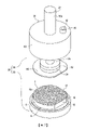
如同上述一般,當在SiC鑄錠2處而形成剝離層28,並將應生成之晶圓56從SiC鑄錠2剝離之後,係實施將SiC鑄錠2之剝離面58平坦化的平坦化方法。在平坦化方法中,係包含有:研削工程,係將剝離面58之相反側藉由可旋轉之吸盤台來作保持,並使以環狀而具備有研削砥石的研削轉盤旋轉,而對於被保持於吸盤台處之SiC鑄錠2之剝離面58進行研削。沿削工程,例如係可使用在圖8中對於其之一部分有所展示的研削裝置60來實施。研削裝置60,係具備有保持SiC鑄錠2之圓形狀之吸盤台62、和對被保持在吸盤台62上的SiC鑄錠2之上面進行研削並使其平坦化之研削手段64。吸盤台62,係與雷射加工裝置18之吸盤台20相同的,成為於上面而將SiC鑄錠2作吸引保持,並且藉由吸盤台用馬達(未圖示),而以通過吸盤台62之徑方向中心並於上下方向而延伸之軸線作為中心來旋轉。研削手段64,係被與轉軸用馬達(未圖示)作連結,並且包含有於上下方向而延伸之圓柱狀之轉軸66、和被固定於轉軸66之下端處的圓板狀之轉盤安裝具68。在轉盤安裝具68之下面處,係藉由螺桿70而被固定有環狀之研削轉盤72。在研削轉盤72之下面的外周緣部處,係被固定有於周方向上空出有間隔地而被配置為環狀之複數之研削砥石74。在研削裝置60處,係以使研削砥石74會通過吸盤台62之旋轉中心的方式,而使研削轉盤72之旋轉中心相對於吸盤台62之旋轉中心而有所位移,在吸盤台62與研削轉盤72一面相互旋轉一面使被保持於吸盤台62之上面處的SiC鑄錠2之上面與研削砥石74作了接觸的情況時,SiC鑄錠2之上面全體係藉由研削砥石74而被作研削。As described above, after the
若是參考圖8而繼續進行說明,則在研削工程中,首先,係在吸盤台62之上面產生吸引力,而將SiC鑄錠2之剝離面58的相反側(基板16側)藉由吸盤台62而作吸引保持。接著,以當從上方觀察時之逆時針方向來以特定之旋轉速度(例如300rpm)而使吸盤台62旋轉。又,係以當從上方觀察時之逆時針方向來以特定之旋轉速度(例如6000rpm)而使轉軸66旋轉。接著,藉由研削裝置60之升降手段(未圖示)來使轉軸66下降,並使研削砥石74與剝離面58相接觸。之後,在使研削砥石74與剝離面58作了接觸之後,以特定之研削饋送速度(例如1.0μm/s)來使轉軸66下降。藉由此,係能夠以當再度於SiC鑄錠2處形成剝離層28時不會對於脈衝雷射光線LB之射入造成妨礙的程度來對SiC鑄錠2之剝離面58進行研削並平坦化。另外,在對於剝離面58進行研削時,係從研削水供給手段(未圖示)來對於剝離面58和研削砥石74而供給研削水。If the description is continued with reference to FIG. 8 , in the grinding process, first, suction is generated on the chuck table 62, and the side opposite to the peeled
於正在實施上述研削工程時,係實施對於從研削轉盤72所露出的SiC鑄錠2之剝離面58照射光並檢測出反射光而檢測出平坦之程度的平坦度檢測工程,並當在平坦度檢測工程中而檢測出剝離面58係成為了平坦時,將研削工程結束。如同圖8中所示一般,平坦度檢測工程,係能夠使用對於從研削轉盤72所露出的剝離面58照射光之發光元件76、和受光被從發光元件76所照射並在剝離面58處而反射了的反射光之受光元件78、和將在剝離面58處的被照射有發光元件76之光之照射位置S(參考圖8(b))的研削水去除之研削水去除手段(未圖示),而實施之。研削水去除手段,係包含被與壓縮空氣源作了連接的噴嘴,並成為從噴嘴來朝向照射位置S噴射壓縮空氣而將在照射位置S處之研削水去除並使剝離面58露出。When the above-mentioned grinding process is being carried out, a flatness detection process is carried out in which the peeled
在平坦度檢測工程中,係在將照射位置S處之研削水去除而使剝離面58露出之後,如同圖9(a)中所示一般地,對於剝離面58而以射入角度θ來從發光元件76而照射光,並藉由反射角度θ來以受光元件78而受光反射光,當受光元件78之受光量超過了臨限值時,係能夠檢測出剝離面58係成為了平坦。亦即是,在將剝離面58平坦化之前,對於剝離面58而以射入角度θ來從發光元件76所對於剝離面58照射之光,由於係會發生散射,因此,以反射角度θ所反射之反射光係為少,受光元件78之受光量係為少,但是,若是剝離面58被平坦化,則由於以反射角度θ所反射之反射光係較平坦化之前而更為增加,受光元件78之受光量係增加,因此,當受光元件78之受光量超過了臨限值時,係能夠檢測出剝離面58係成為了平坦。如同圖9(b)中所示一般,臨限值Rc,係能夠在平坦化前之受光量之平均值R1與平坦化後之受光量之平均值R2之間而任意作設定,但是,較理想,係身為較平均值R1與平均值R2之間之中間值而更接近平均值R2之值。In the flatness inspection process, after the grinding water at the irradiation position S is removed to expose the peeling
又,係亦可構成為:在平坦度檢測工程中,當從藉由c面和端面而形成了斷開角α(亦即是,斷開角α係並非為0度)之SiC鑄錠2的剝離層28而將應產生之晶圓56作了剝離的情況時,係如同圖10(a)中所示一般,對於剝離面58而垂直地從發光元件76來照射光,並在與發光元件76之間所成之角度成為2α的位置處藉由受光元件78來受光反射光,當受光量為低於臨限值時,檢測出剝離面58係成為了平坦。亦即是,當從藉由c面和端面而形成了斷開角α之SiC鑄錠2的剝離層28而將應產生之晶圓56作了剝離的情況時,由於在剝離面58處係存在有沿著c面而延伸之部分,因此,被配置在與發光元件76之間所成之角度成為2α的位置處之受光元件78所受光的受光量,當在剝離面58之研削中而成為了圖10(a)中所示之位置關係時係會變得較大,並成為如同圖10(b)中所示一般地而變動。而,若是剝離面58被平坦化,則由於在剝離面58處沿著c面而延伸之部分係消失,因此係成為並不會被檢測出之前所被斷續性地檢測出的較大之值之受光量。故而,在受光元件78之受光量成為低於臨限值時(亦即是,成為不會檢測出臨限值以上之受光量時),係能夠檢測出剝離面58係成為了平坦。如同圖10(b)中所示一般,於此情況下之臨限值Rc,係能夠在平坦化前而被斷續性地檢測出之較大之值的受光量之平均值R3與平坦化後之受光量之平均值R4之間而任意作設定,但是,較理想,係身為較平均值R3與平均值R4之間之中間值而更接近平均值R4之值。另外,在上述之「對於剝離面58而垂直地從發光元件76照射光」中的「對於剝離面58而垂直」,係指相對於研削後之平坦之剝離面58而為垂直。In addition, the system can also be configured as follows: in the flatness inspection process, when the
如同上述一般,在本實施形態中,由於係包含有:研削工程,係將SiC鑄錠2之剝離面58之相反側藉由可旋轉之吸盤台62來作保持,並使以環狀而具備有研削砥石74的研削轉盤72旋轉,而對於被保持於吸盤台62處之SiC鑄錠2之剝離面58進行研削;和平坦度檢測工程,係對於從研削轉盤72而露出的SiC鑄錠2之剝離面58照射光,並檢測出反射光,而檢測出平坦之程度,當在平坦度檢測工程中而檢測出SiC鑄錠2之剝離面58係成為了平坦時,係將研削工程結束,因此,係能夠避免剝離面58之過度的研削,而將研削時間縮短。As mentioned above, in this embodiment, since the grinding process is included, the opposite side of the peeled
2‧‧‧SiC鑄錠4‧‧‧第1端面6‧‧‧第2端面26‧‧‧碎裂28‧‧‧剝離層56‧‧‧晶圓58‧‧‧SiC鑄錠之剝離面62‧‧‧研削裝置之吸盤台72‧‧‧研削轉盤74‧‧‧研削砥石LB‧‧‧脈衝雷射光線FP‧‧‧集光點2‧‧‧
[圖1](a)係為SiC鑄錠之正面圖,(b)係為SiC鑄錠之平面圖。 [圖2](a)係為SiC鑄錠以及基板之立體圖,(b)係為對於在SiC鑄錠處被裝著有基板之狀態作展示的立體圖。 [圖3]係為對於在雷射加工裝置之吸盤台處載置有SiC鑄錠的狀態作展示之立體圖。 [圖4](a)係為對於正被實施剝離層形成工程之狀態作展示的立體圖,(b)係為對於正被實施剝離層形成工程之狀態作展示的正面圖。 [圖5](a)係為被形成有剝離層的SiC鑄錠的平面圖,(b)係為(a)中之B-B線剖面圖。 [圖6]係為剝離裝置之剖面圖。 [圖7]係為對於藉由剝離裝置來使晶圓從鑄錠而剝離後的狀態作展示之立體圖。 [圖8](a)係為對於正被實施研削工程以及平坦度檢測工程之狀態作展示的立體圖,(b)係為對於SiC鑄錠之剝離面被作了平坦化的狀態作展示之立體圖。 [圖9](a)係為針對對於剝離面而以射入角度θ來照射光並藉由反射角度θ來受光反射光的狀態作展示之示意圖,(b)係為對於在(a)的情況中之受光量的歷時變化作展示之圖表。 [圖10](a)係為針對對於剝離面而垂直地照射光並在距離照射位置而角度為2α的位置來受光反射光的狀態作展示之示意圖,(b)係為對於在(a)的情況中之受光量的歷時變化作展示之圖表。[Fig. 1] (a) is the front view of the SiC ingot, and (b) is the plan view of the SiC ingot. [Fig. 2] (a) is a perspective view of the SiC ingot and the substrate, and (b) is a perspective view showing the state where the substrate is mounted on the SiC ingot. [Fig. 3] is a perspective view showing a state in which a SiC ingot is placed on a chuck table of a laser processing device. [Fig. 4] (a) is a perspective view showing a state where a peeling layer forming process is being implemented, and (b) is a front view showing a state where a peeling layer forming process is being implemented. [Fig. 5] (a) is a plan view of a SiC ingot formed with a peeling layer, and (b) is a cross-sectional view along line B-B in (a). [Figure 6] is a sectional view of the stripping device. [Fig. 7] is a perspective view showing the state after the wafer is peeled from the ingot by the peeling device. [Fig. 8] (a) is a perspective view showing the state where the grinding process and flatness inspection process are being carried out, and (b) is a perspective view showing the state where the peeled surface of the SiC ingot is flattened . [Fig. 9] (a) is a schematic diagram showing the state of irradiating the peeling surface with light at an incident angle θ and receiving reflected light at a reflection angle θ, and (b) is a schematic diagram showing the state in (a) A graph showing the time-dependent changes in the amount of received light under conditions. [Fig. 10] (a) is a schematic diagram showing the state where light is irradiated perpendicularly to the peeling surface and reflected light is received at a position with an angle of 2α from the irradiated position, and (b) is a schematic diagram showing the state of light reflected in (a) Graphs showing the time-dependent changes in light received in the case.
2‧‧‧SiC鑄錠 2‧‧‧SiC ingot
6‧‧‧第2端面 6‧‧‧The second end face
8‧‧‧周面 8‧‧‧Week noodles
12‧‧‧第1定向平面 12‧‧‧The first orientation plane
16‧‧‧基板 16‧‧‧substrate
58‧‧‧SiC鑄錠之剝離面 58‧‧‧Splitting surface of SiC ingot
60‧‧‧研削裝置 60‧‧‧Grinding device
62‧‧‧研削裝置之吸盤台 62‧‧‧Suction cup table for grinding device
64‧‧‧研削手段 64‧‧‧Grinding means
66‧‧‧轉軸 66‧‧‧Rotating shaft
68‧‧‧轉盤安裝具 68‧‧‧Turntable installation
70‧‧‧螺桿 70‧‧‧Screw
72‧‧‧研削轉盤 72‧‧‧Grinding turntable
74‧‧‧研削砥石 74‧‧‧grinding whetstone
76‧‧‧發光元件 76‧‧‧Light-emitting components
78‧‧‧受光元件 78‧‧‧light receiving element
S‧‧‧照射位置 S‧‧‧irradiation position
Claims (1)
Applications Claiming Priority (2)
| Application Number | Priority Date | Filing Date | Title |
|---|---|---|---|
| JP2018005046A JP7009224B2 (en) | 2018-01-16 | 2018-01-16 | Flattening method |
| JP2018-005046 | 2018-01-16 |
Publications (2)
| Publication Number | Publication Date |
|---|---|
| TW201933465A TW201933465A (en) | 2019-08-16 |
| TWI793246B true TWI793246B (en) | 2023-02-21 |
Family
ID=67068966
Family Applications (1)
| Application Number | Title | Priority Date | Filing Date |
|---|---|---|---|
| TW108101138A TWI793246B (en) | 2018-01-16 | 2019-01-11 | planarization method |
Country Status (8)
| Country | Link |
|---|---|
| US (1) | US10714353B2 (en) |
| JP (1) | JP7009224B2 (en) |
| KR (1) | KR102549852B1 (en) |
| CN (1) | CN110047746B (en) |
| DE (1) | DE102019200383B4 (en) |
| MY (1) | MY198101A (en) |
| SG (1) | SG10201900044RA (en) |
| TW (1) | TWI793246B (en) |
Families Citing this family (20)
| Publication number | Priority date | Publication date | Assignee | Title |
|---|---|---|---|---|
| JP7009194B2 (en) * | 2017-12-12 | 2022-01-25 | 株式会社ディスコ | Wafer generator and transport tray |
| JP7164396B2 (en) * | 2018-10-29 | 2022-11-01 | 株式会社ディスコ | wafer generator |
| US10562130B1 (en) | 2018-12-29 | 2020-02-18 | Cree, Inc. | Laser-assisted method for parting crystalline material |
| US11024501B2 (en) | 2018-12-29 | 2021-06-01 | Cree, Inc. | Carrier-assisted method for parting crystalline material along laser damage region |
| US10576585B1 (en) | 2018-12-29 | 2020-03-03 | Cree, Inc. | Laser-assisted method for parting crystalline material |
| US10611052B1 (en) | 2019-05-17 | 2020-04-07 | Cree, Inc. | Silicon carbide wafers with relaxed positive bow and related methods |
| CN110752169B (en) * | 2019-10-21 | 2022-03-22 | 西安奕斯伟材料科技有限公司 | A wafer processing device and loading and unloading method |
| JP7321888B2 (en) * | 2019-10-24 | 2023-08-07 | 株式会社ディスコ | SiC ingot processing method and laser processing apparatus |
| JP7405649B2 (en) * | 2020-03-04 | 2023-12-26 | 株式会社ディスコ | Grinding method of workpiece |
| JP2021183359A (en) * | 2020-05-21 | 2021-12-02 | 株式会社ディスコ | Grinding device |
| JP7547105B2 (en) * | 2020-07-29 | 2024-09-09 | 株式会社ディスコ | Si substrate production method |
| JP7657043B2 (en) * | 2020-12-07 | 2025-04-04 | 株式会社ディスコ | Wafer Generation Equipment |
| JP7648375B2 (en) * | 2020-12-17 | 2025-03-18 | 株式会社ディスコ | Wafer Generation Equipment |
| JP7561605B2 (en) * | 2020-12-23 | 2024-10-04 | 株式会社ディスコ | Grinding Equipment |
| CN113130305B (en) * | 2021-03-03 | 2023-03-24 | 哈尔滨工业大学 | Method for constructing surface microstructure of silicon carbide single crystal |
| JP7629791B2 (en) * | 2021-04-15 | 2025-02-14 | 株式会社ディスコ | Laser processing equipment |
| JP7637566B2 (en) * | 2021-06-01 | 2025-02-28 | 東京エレクトロン株式会社 | Processing system and processing method |
| JP7728108B2 (en) * | 2021-06-23 | 2025-08-22 | 株式会社ディスコ | Peeling device |
| CN116147541A (en) * | 2021-11-23 | 2023-05-23 | 成都辰显光电有限公司 | Detection device and detection method |
| JP2023170392A (en) * | 2022-05-19 | 2023-12-01 | 株式会社ディスコ | Peeling device |
Citations (2)
| Publication number | Priority date | Publication date | Assignee | Title |
|---|---|---|---|---|
| US20070042693A1 (en) * | 2005-08-18 | 2007-02-22 | Saikin Alan H | Polishing pad and method of manufacture |
| US20170301549A1 (en) * | 2016-04-19 | 2017-10-19 | Disco Corporation | METHOD OF PROCESSING SiC WAFER |
Family Cites Families (6)
| Publication number | Priority date | Publication date | Assignee | Title |
|---|---|---|---|---|
| JPH02222533A (en) * | 1989-02-23 | 1990-09-05 | Sumitomo Electric Ind Ltd | Polishing device for semiconductor wafer |
| JP2000094221A (en) | 1998-09-24 | 2000-04-04 | Toyo Advanced Technologies Co Ltd | Electric discharge wire saw |
| JP6179021B2 (en) * | 2013-07-18 | 2017-08-16 | 株式会社岡本工作機械製作所 | Semiconductor substrate flattening grinding method |
| JP6399913B2 (en) | 2014-12-04 | 2018-10-03 | 株式会社ディスコ | Wafer generation method |
| JP6478821B2 (en) * | 2015-06-05 | 2019-03-06 | 株式会社ディスコ | Wafer generation method |
| JP6637831B2 (en) * | 2016-04-28 | 2020-01-29 | 株式会社ディスコ | Device manufacturing method and grinding device |
-
2018
- 2018-01-16 JP JP2018005046A patent/JP7009224B2/en active Active
- 2018-12-27 KR KR1020180170230A patent/KR102549852B1/en active Active
-
2019
- 2019-01-02 MY MYPI2019000204A patent/MY198101A/en unknown
- 2019-01-03 SG SG10201900044RA patent/SG10201900044RA/en unknown
- 2019-01-04 CN CN201910007502.XA patent/CN110047746B/en active Active
- 2019-01-10 US US16/244,867 patent/US10714353B2/en active Active
- 2019-01-11 TW TW108101138A patent/TWI793246B/en active
- 2019-01-15 DE DE102019200383.4A patent/DE102019200383B4/en active Active
Patent Citations (2)
| Publication number | Priority date | Publication date | Assignee | Title |
|---|---|---|---|---|
| US20070042693A1 (en) * | 2005-08-18 | 2007-02-22 | Saikin Alan H | Polishing pad and method of manufacture |
| US20170301549A1 (en) * | 2016-04-19 | 2017-10-19 | Disco Corporation | METHOD OF PROCESSING SiC WAFER |
Also Published As
| Publication number | Publication date |
|---|---|
| CN110047746A (en) | 2019-07-23 |
| TW201933465A (en) | 2019-08-16 |
| JP2019125687A (en) | 2019-07-25 |
| SG10201900044RA (en) | 2019-08-27 |
| US20190221436A1 (en) | 2019-07-18 |
| DE102019200383A1 (en) | 2019-07-18 |
| JP7009224B2 (en) | 2022-01-25 |
| US10714353B2 (en) | 2020-07-14 |
| KR20190087287A (en) | 2019-07-24 |
| DE102019200383B4 (en) | 2024-03-21 |
| MY198101A (en) | 2023-08-01 |
| CN110047746B (en) | 2024-02-20 |
| KR102549852B1 (en) | 2023-06-29 |
Similar Documents
| Publication | Publication Date | Title |
|---|---|---|
| TWI793246B (en) | planarization method | |
| KR102691687B1 (en) | Method for forming wafer | |
| TWI782138B (en) | Wafer production method and wafer production device | |
| JP6959120B2 (en) | Peeling device | |
| TWI752148B (en) | Method for producing silicon carbide (SiC) wafers | |
| US10056263B2 (en) | Method of processing SiC wafer | |
| JP7027215B2 (en) | Wafer generation method and wafer generation device | |
| TWI779173B (en) | Wafer production method and wafer production device | |
| TWI748088B (en) | SiC wafer generation method | |
| CN110071034B (en) | Wafer production method and wafer production device | |
| JP7187215B2 (en) | SiC substrate processing method | |
| TW201926535A (en) | Peeling apparatus | |
| TW202030474A (en) | Fact area detection method and detection device, wafer generation method and laser processing device | |
| TW201929131A (en) | Wafer generation device and transfer tray | |
| TW201829862A (en) | SiC wafer producing method | |
| TW201835995A (en) | Wafer producing method capable of efficiently delaminating a wafer from a mono-crystalline SiC ingot | |
| TWI807083B (en) | Processing method of semiconductor substrate | |
| TW202140870A (en) | Wafer production method | |
| JP2023116216A (en) | Wafer generation method |