TWI788390B - A distributed electrode array for plasma processing - Google Patents

A distributed electrode array for plasma processing Download PDF

Info

Publication number
TWI788390B
TWI788390B TW107126405A TW107126405A TWI788390B TW I788390 B TWI788390 B TW I788390B TW 107126405 A TW107126405 A TW 107126405A TW 107126405 A TW107126405 A TW 107126405A TW I788390 B TWI788390 B TW I788390B
Authority
TW
Taiwan
Prior art keywords
electrode
split
electrodes
power
source assembly
Prior art date
Application number
TW107126405A
Other languages
Chinese (zh)
Other versions
TW201911974A (en
Inventor
肯尼士S 柯林斯
麥可R 萊斯
卡提克 拉馬斯瓦米
詹姆士D 卡度希
郭岳
歐嘉 瑞杰門
Original Assignee
美商應用材料股份有限公司
Priority date (The priority date is an assumption and is not a legal conclusion. Google has not performed a legal analysis and makes no representation as to the accuracy of the date listed.)
Filing date
Publication date
Application filed by 美商應用材料股份有限公司 filed Critical 美商應用材料股份有限公司
Publication of TW201911974A publication Critical patent/TW201911974A/en
Application granted granted Critical
Publication of TWI788390B publication Critical patent/TWI788390B/en

Links

Images

Classifications

    • HELECTRICITY
    • H01ELECTRIC ELEMENTS
    • H01JELECTRIC DISCHARGE TUBES OR DISCHARGE LAMPS
    • H01J37/00Discharge tubes with provision for introducing objects or material to be exposed to the discharge, e.g. for the purpose of examination or processing thereof
    • H01J37/32Gas-filled discharge tubes
    • H01J37/32009Arrangements for generation of plasma specially adapted for examination or treatment of objects, e.g. plasma sources
    • H01J37/32082Radio frequency generated discharge
    • H01J37/32174Circuits specially adapted for controlling the RF discharge
    • HELECTRICITY
    • H01ELECTRIC ELEMENTS
    • H01JELECTRIC DISCHARGE TUBES OR DISCHARGE LAMPS
    • H01J37/00Discharge tubes with provision for introducing objects or material to be exposed to the discharge, e.g. for the purpose of examination or processing thereof
    • H01J37/32Gas-filled discharge tubes
    • H01J37/32009Arrangements for generation of plasma specially adapted for examination or treatment of objects, e.g. plasma sources
    • H01J37/32082Radio frequency generated discharge
    • H01J37/321Radio frequency generated discharge the radio frequency energy being inductively coupled to the plasma
    • H01J37/3211Antennas, e.g. particular shapes of coils
    • HELECTRICITY
    • H01ELECTRIC ELEMENTS
    • H01JELECTRIC DISCHARGE TUBES OR DISCHARGE LAMPS
    • H01J37/00Discharge tubes with provision for introducing objects or material to be exposed to the discharge, e.g. for the purpose of examination or processing thereof
    • H01J37/32Gas-filled discharge tubes
    • H01J37/32009Arrangements for generation of plasma specially adapted for examination or treatment of objects, e.g. plasma sources
    • H01J37/32082Radio frequency generated discharge
    • H01J37/32137Radio frequency generated discharge controlling of the discharge by modulation of energy
    • H01J37/32155Frequency modulation
    • H01J37/32165Plural frequencies
    • HELECTRICITY
    • H01ELECTRIC ELEMENTS
    • H01JELECTRIC DISCHARGE TUBES OR DISCHARGE LAMPS
    • H01J37/00Discharge tubes with provision for introducing objects or material to be exposed to the discharge, e.g. for the purpose of examination or processing thereof
    • H01J37/32Gas-filled discharge tubes
    • H01J37/32431Constructional details of the reactor
    • H01J37/3244Gas supply means
    • HELECTRICITY
    • H01ELECTRIC ELEMENTS
    • H01JELECTRIC DISCHARGE TUBES OR DISCHARGE LAMPS
    • H01J37/00Discharge tubes with provision for introducing objects or material to be exposed to the discharge, e.g. for the purpose of examination or processing thereof
    • H01J37/32Gas-filled discharge tubes
    • H01J37/32431Constructional details of the reactor
    • H01J37/32532Electrodes
    • H01J37/32568Relative arrangement or disposition of electrodes; moving means

Landscapes

  • Physics & Mathematics (AREA)
  • Engineering & Computer Science (AREA)
  • Plasma & Fusion (AREA)
  • Chemical & Material Sciences (AREA)
  • Analytical Chemistry (AREA)
  • Plasma Technology (AREA)
  • Drying Of Semiconductors (AREA)
  • Electrical Discharge Machining, Electrochemical Machining, And Combined Machining (AREA)

Abstract

Embodiments of the disclosure provide a plasma source assembly and process chamber design that can be used for any number of substrate processing techniques. The plasma source may include a plurality of discrete electrodes that are integrated with a reference electrode and a gas feed structure to generate a uniform, stable and repeatable plasma during processing. The plurality of discrete electrodes include an array of electrodes that can be biased separately, in groups, or all in unison relative to a reference electrode. The plurality of discrete electrodes may include a plurality of conductive rods that are positioned to generate a plasma within a processing region of a process chamber. The plurality of discrete electrodes is provided RF power from standing or traveling waves imposed on a power distribution element to which the electrodes are connected.

Description

用於電漿處理的分佈式電極陣列Distributed Electrode Arrays for Plasma Treatment

本揭示之實施例一般係關於半導體處理裝備。更特定言之,本揭示之實施例係關於用於產生電漿以處理基板的電極組件。Embodiments of the present disclosure relate generally to semiconductor processing equipment. More particularly, embodiments of the present disclosure relate to electrode assemblies for generating plasma for processing substrates.

積體電路已經發展成複雜的裝置,而可以在單一晶片上包括數百萬個部件(例如,電晶體、電容器、電阻器、及類似者)。晶片設計的發展需要更快的電路以及更大的電路密度,而對更大電路密度的需求則需要減少積體電路部件的尺寸。這種裝置的特徵的最小尺寸在該領域中通常稱為臨界尺寸,並且通常包括電路結構的特徵的最小寬度(例如,線段、線段之間的空間、柱、開口、及類似者)。Integrated circuits have grown into complex devices that can include millions of components (eg, transistors, capacitors, resistors, and the like) on a single chip. Advances in chip designs require faster circuits and greater circuit densities, and the need for greater circuit densities requires reductions in the size of integrated circuit components. The minimum dimensions of features of such devices are often referred to in the art as critical dimensions, and typically include the minimum widths of features of circuit structures (eg, line segments, spaces between line segments, posts, openings, and the like).

隨著這些臨界尺寸的縮小,整個基板的處理均勻性變得重要,以維持高產量。用於製造當今所需的增加的更小幾何形狀的積體電路的習知電漿處理與習知腔室設計無法滿足在電漿處理期間整個基板上所需的沉積或蝕刻速率均勻性的要求,這對於成功的半導體裝置製造是必要的。隨著裝置幾何尺寸的縮小及基板大小的增加,這種均勻性變得越來越難以實現。處理非均勻性(例如,腔室設計不對稱性、溫度分佈不均勻性、及氣體分佈控制)的各種來源變得越來越重要。而且,習知電容耦合電漿源(CCP)與電感耦合電漿源(ICP)存在一些問題(包括不希望的電漿及處理均勻性,以及差的處理可重複性)。舉例而言,習知電感耦合電漿源可以在腔室頂板上方具有二個同心佈置的線圈天線,而可以藉由調整傳遞到不同線圈天線的不同RF功率等級來最佳化蝕刻速率分佈的均勻性。但是,隨著工件直徑與腔室直徑的增加,我們發現此方式並不適用,因為較大的尺寸增加了取得必要的處理均勻性的難度。而且,在習知CCP與ICP電漿源中,不希望的材料濺射或蝕刻可能導致處理污染或顆粒形成,這可能是由於驅動或接地電極表面或ICP窗口表面處的過量離子能量。As these critical dimensions shrink, process uniformity across the substrate becomes important to maintain high throughput. Conventional plasma processing and conventional chamber designs for fabricating the increasingly smaller geometries of integrated circuits required today cannot meet the required uniformity of deposition or etch rates across the substrate during plasma processing , which is necessary for successful semiconductor device fabrication. This uniformity becomes increasingly difficult to achieve as device geometries shrink and substrate sizes increase. It is becoming increasingly important to address various sources of non-uniformity (eg, chamber design asymmetry, temperature distribution non-uniformity, and gas distribution control). Furthermore, conventional capacitively coupled plasma (CCP) and inductively coupled plasma (ICP) sources suffer from several problems (including undesired plasma and process uniformity, and poor process repeatability). For example, a conventional ICP source can have two coil antennas arranged concentrically above the chamber ceiling, and the uniformity of etch rate distribution can be optimized by adjusting different RF power levels delivered to the different coil antennas. sex. However, as the workpiece diameter and chamber diameter increased, we found that this approach was not suitable, as the larger size increased the difficulty in achieving the necessary process uniformity. Also, in conventional CCP and ICP plasma sources, undesired material sputtering or etching can lead to process contamination or particle formation, possibly due to excess ion energy at the drive or ground electrode surfaces or the ICP window surfaces.

在一些電漿處理腔室或系統中,工件在例如線性或旋轉工件支撐件上移動通過電漿處理區域。在這樣的腔室中,移動工件支撐電路可能不是低阻抗(相對於電漿阻抗)RF接地路徑,即使可以通過例如旋轉汞耦合器、電刷、或滑環而進行DC接地。缺乏足夠的RF接地路徑可能造成難以控制工件處的離子能量或者使得電漿處理(例如,沉積或蝕刻處理)的可重複性變差。In some plasma processing chambers or systems, a workpiece is moved through the plasma processing region on, for example, a linear or rotating workpiece support. In such chambers, the moving workpiece support circuit may not be a low impedance (relative to plasma impedance) path to RF ground, even though a DC ground may be provided by, for example, a rotating mercury coupler, brushes, or slip rings. Lack of an adequate RF ground path can make it difficult to control ion energy at the workpiece or make plasma processing (eg, deposition or etch processing) less repeatable.

因此,需要一種能夠有效地產生具有所期望性質(例如,離解度、組成、自由基密度或通量、離子密度、電子密度、電子溫度、離子能量分佈等)的均勻電漿,可在操作窗口上諧調,具有穩定且可重複的性能,不產生粒子,並具有可接受的硬體壽命的電漿源及/或處理腔室。Therefore, there is a need for a method that can efficiently generate a homogeneous plasma with desired properties (e.g., degree of dissociation, composition, radical density or flux, ion density, electron density, electron temperature, ion energy distribution, etc.) A plasma source and/or process chamber that is up-tuned, has stable and repeatable performance, does not generate particles, and has acceptable hardware lifetime.

提供一種用於處理腔室的電漿源組件,而在一個實施例中包括相對於參考電極定位的複數個分離電極,並在一些情況下在處理期間相對於氣體饋送結構產生均勻、穩定、且可重複的電漿。A plasma source assembly for a processing chamber is provided, and in one embodiment includes a plurality of separate electrodes positioned relative to a reference electrode, and in some cases generating uniform, stable, and Repeatable plasma.

本文提供的本揭示的實施例包括電漿源組件,包括具有跨越第一平面分佈的電極表面的參考電極,以及以跨越第一平面分佈的圖案來佈置的分離電極的陣列。分離電極的圖案可以形成為分佈在平行於第一平面的二個非平行方向上的陣列。分離電極可以平行對準到以一角度與第一平面定向的第一方向,並且具有在基本垂直於第一平面的方向上設置於距離表面的第一距離的端部。Embodiments of the disclosure provided herein include a plasma source assembly including a reference electrode having an electrode surface distributed across a first plane, and an array of separate electrodes arranged in a pattern distributed across the first plane. The pattern of the separated electrodes may be formed as an array distributed in two non-parallel directions parallel to the first plane. The split electrodes may be aligned parallel to a first direction oriented at an angle to the first plane and have ends disposed a first distance from the surface in a direction substantially perpendicular to the first plane.

本揭示的實施例可以進一步提供電漿源組件,電漿源組件包括連接到複數個分離電極的功率分佈元件,其中分離電極係以跨越表面分佈的圖案佈置,而分離電極中之每一者包括在基本垂直於表面的方向上設置成距離表面第一距離的端部。電漿源組件亦可包括RF訊號產生器與匹配網路,RF訊號產生器提供RF功率,而匹配網路係從RF訊號產生器接收RF功率,並將RF功率提供到功率分佈元件上的至少二個連接點。Embodiments of the present disclosure may further provide a plasma source assembly comprising a power distribution element connected to a plurality of split electrodes, wherein the split electrodes are arranged in a pattern distributed across a surface, each of the split electrodes comprising An end disposed at a first distance from the surface in a direction substantially perpendicular to the surface. The plasma source assembly may also include an RF signal generator that provides RF power, and a matching network that receives RF power from the RF signal generator and provides RF power to at least one of the power distribution elements. Two connection points.

本揭示的實施例可以進一步提供電漿源組件,電漿源組件包括連接到複數個分離電極的功率分佈元件,以將RF功率提供至複數個分離電極,其中分離電極係以跨越表面分佈的圖案佈置,而分離電極中之每一者包括在基本垂直於表面的方向上設置成距離表面第一距離的端部。電漿源組件亦可包括第一RF產生器、第二RF產生器、相位偵測器、及相位控制器,第一RF產生器具有用於接收第一RF控制訊號的輸入以及用於將RF功率提供至功率分佈元件上的第一連接點的輸出,第二RF產生器具有用於接收第二RF控制訊號的輸入以及用於將RF功率提供至功率分佈元件上的第二連接點的輸出,相位偵測器經配置以偵測來自第一RF產生器的輸出與來自第二RF產生器的輸出的相位差,相位控制器係從相位偵測器接收所偵測的相位差,並產生相位偏移控制訊號,以用於改變從第一RF產生器遞送的輸出的相位。Embodiments of the present disclosure may further provide a plasma source assembly comprising a power distribution element connected to a plurality of split electrodes to provide RF power to the plurality of split electrodes, wherein the split electrodes are in a pattern distributed across a surface arranged, and each of the separated electrodes includes an end portion disposed at a first distance from the surface in a direction substantially perpendicular to the surface. The plasma source assembly may also include a first RF generator, a second RF generator, a phase detector, and a phase controller, the first RF generator having an input for receiving a first RF control signal and for applying RF power to providing an output to a first connection point on the power distribution element, a second RF generator having an input for receiving a second RF control signal and an output for providing RF power to a second connection point on the power distribution element, the phase The detector is configured to detect a phase difference between an output from the first RF generator and an output from the second RF generator, and the phase controller receives the detected phase difference from the phase detector and generates a phase offset A shift control signal for changing the phase of the output delivered from the first RF generator.

本揭示的實施例可以進一步提供電漿源組件,電漿源組件包括連接到複數個分離電極的功率分佈元件,以將RF功率提供至複數個分離電極,其中分離電極係以跨越表面分佈的圖案佈置,而分離電極中之每一者包括在基本垂直於表面的方向上設置成距離表面第一距離的端部。電漿源組件亦可包括第一RF產生器、第二RF產生器、相位偏移器、訊號產生器、相位偵測器、及相位控制器,第一RF產生器具有用於接收第一RF控制訊號的輸入以及用於將RF功率提供至功率分佈元件上的第一連接點的輸出,第二RF產生器具有用於接收第二RF控制訊號的輸入以及用於將RF功率提供至功率分佈元件上的第二連接點的輸出,相位偏移器係將第一RF控制訊號提供至第一RF產生器的輸入,以回應於相位偏移控制訊號與第二RF控制訊號,訊號產生器將第二RF訊號提供至相位偏移器以及第二RF產生器的輸入,相位偵測器經配置以偵測來自第一RF產生器的輸出與來自第二RF產生器的輸出的相位差,相位控制器係從相位偵測器接收所偵測的相位差,並將相位偏移控制訊號提供至相位偏移器,以改變第一RF訊號的相位。Embodiments of the present disclosure may further provide a plasma source assembly comprising a power distribution element connected to a plurality of split electrodes to provide RF power to the plurality of split electrodes, wherein the split electrodes are in a pattern distributed across a surface arranged, and each of the separated electrodes includes an end portion disposed at a first distance from the surface in a direction substantially perpendicular to the surface. The plasma source assembly may also include a first RF generator, a second RF generator, a phase shifter, a signal generator, a phase detector, and a phase controller, the first RF generator having a control function for receiving the first RF a signal input and an output for providing RF power to a first connection point on the power distribution element, a second RF generator has an input for receiving a second RF control signal and for providing RF power to the power distribution element The output of the second connection point of the phase shifter is to provide the first RF control signal to the input of the first RF generator, in response to the phase shift control signal and the second RF control signal, the signal generator will be the second The RF signal is provided to the phase shifter and the input of the second RF generator, the phase detector is configured to detect the phase difference between the output from the first RF generator and the output from the second RF generator, the phase controller The detected phase difference is received from the phase detector, and the phase shift control signal is provided to the phase shifter to change the phase of the first RF signal.

本揭示的實施例可以進一步提供電漿源組件,電漿源組件包括連接到複數個分離電極的功率分佈元件,以將RF功率提供至複數個分離電極,其中分離電極係以跨越表面延伸的圖案佈置,而分離電極中之每一者包括在基本垂直於表面的方向上設置成距離表面第一距離的端部。電漿源組件亦可包括第一循環器、第二循環器、第一RF產生器、及第二RF產生器,第一循環器包括第一、第二、及第三埠,第二埠經由第一匹配網路在第一位置處將RF功率提供至功率分佈元件,而第三埠連接至第一虛擬負載,第二循環器包括第一、第二、及第三埠,第二埠經由第二匹配網路在功率分佈元件上的第二位置處提供RF功率,而第三埠連接至第二虛擬負載,第一RF產生器以第一頻率將RF功率提供至第一循環器的第一埠,第二RF產生器以第二頻率將RF功率提供至第二循環器的第一埠。Embodiments of the present disclosure may further provide a plasma source assembly comprising a power distribution element connected to a plurality of split electrodes to provide RF power to the plurality of split electrodes, wherein the split electrodes are in a pattern extending across a surface arranged, and each of the separated electrodes includes an end portion disposed at a first distance from the surface in a direction substantially perpendicular to the surface. The plasma source assembly may also include a first circulator, a second circulator, a first RF generator, and a second RF generator, the first circulator includes first, second, and third ports, and the second port passes through The first matching network provides RF power to the power distribution element at the first location, and the third port is connected to the first dummy load, the second circulator includes the first, second, and third ports, and the second port is connected via The second matching network provides RF power at a second location on the power distribution element, while the third port is connected to a second dummy load, and the first RF generator provides RF power at a first frequency to the second port of the first circulator. A second RF generator provides RF power to the first port of the second circulator at a second frequency.

本揭示的實施例可以進一步提供一種在處理腔室的處理區域中形成電漿的方法,該方法包括以下步驟:將RF功率從第一RF產生器遞送到複數個分離電極,其中從第一RF產生器遞送RF功率包含以下步驟:將RF功率提供至耦接至複數個分離電極的功率分佈元件上的第一連接點,而複數個分離電極中之每一者包含在基本垂直於表面的方向上設置成距離表面第一距離的端部;從第二RF產生器將RF功率遞送到複數個分離電極,其中從第二RF產生器遞送RF功率包括以下步驟:將RF功率提供至功率分佈元件上的第二連接點;以及相對於從第二RF產生器遞送到功率分佈元件的RF功率的相位,控制從第一RF產生器遞送到功率分佈元件的RF功率的相位。Embodiments of the present disclosure may further provide a method of forming a plasma in a processing region of a processing chamber, the method comprising the steps of: delivering RF power from a first RF generator to a plurality of split electrodes, wherein from the first RF The generator delivering RF power comprises the steps of: providing RF power to a first connection point on a power distribution element coupled to a plurality of separate electrodes, each of the plurality of separate electrodes being comprised in a direction substantially perpendicular to the surface an end disposed at a first distance from the surface; delivering RF power from a second RF generator to the plurality of separate electrodes, wherein delivering RF power from the second RF generator comprises the steps of: providing RF power to a power distribution element and controlling the phase of the RF power delivered from the first RF generator to the power distribution element relative to the phase of the RF power delivered to the power distribution element from the second RF generator.

本揭示的實施例可以進一步提供一種在處理腔室的處理區域中形成電漿的方法,該方法包括以下步驟:將第一RF訊號遞送到複數個分離電極,其中遞送第一RF訊號包含以下步驟:將RF電流遞送到或者將RF電壓施加至耦接到複數個分離電極的功率分佈元件上的第一連接點,複數個分離電極包含在基本垂直於表面的方向上設置成距離表面第一距離的端部;將第二RF訊號遞送到複數個分離電極,其中遞送第二RF訊號包含以下步驟:將RF電流遞送到或將RF電壓施加至耦接到複數個分離電極的功率分佈元件上的第二連接點;以及選擇第一RF訊號的頻率與第二RF訊號的頻率,而使得遞送到複數個分離電極的第一RF訊號與第二RF訊號在處理區域中產生電漿,其中第一RF訊號的頻率不同於第二RF訊號的頻率。Embodiments of the present disclosure may further provide a method of forming a plasma in a processing region of a processing chamber, the method comprising the steps of: delivering a first RF signal to a plurality of separate electrodes, wherein delivering the first RF signal comprises the steps of : delivering RF current to or applying RF voltage to a first connection point on a power distribution element coupled to a plurality of separate electrodes comprising a first distance from the surface in a direction substantially perpendicular to the surface delivering a second RF signal to the plurality of split electrodes, wherein delivering the second RF signal comprises the steps of: delivering an RF current to or applying an RF voltage to a power distribution element coupled to the plurality of split electrodes a second connection point; and selecting the frequency of the first RF signal and the frequency of the second RF signal such that the first RF signal and the second RF signal delivered to the plurality of separate electrodes generate a plasma in the treatment region, wherein the first The frequency of the RF signal is different from the frequency of the second RF signal.

本揭示的實施例可以進一步提供一種在處理腔室的處理區域中形成電漿的方法,該方法包括以下步驟:將第一RF訊號遞送到複數個分離電極,其中遞送第一RF訊號包括以下步驟:將RF電流遞送到或將RF電壓施加至耦接到複數個分離電極的功率分佈元件上的第一連接點,其中複數個分離電極中之每一者包含在基本垂直於參考電極的表面的方向上設置成距離該表面第一距離的端部;以及將第一RF訊號遞送到複數個分離電極,而使得在功率分佈元件中形成行進波,並在處理區域中形成電漿。Embodiments of the present disclosure may further provide a method of forming a plasma in a processing region of a processing chamber, the method comprising the steps of: delivering a first RF signal to a plurality of separate electrodes, wherein delivering the first RF signal comprises the steps of : delivering an RF current to or applying an RF voltage to a first connection point on a power distribution element coupled to a plurality of separate electrodes, wherein each of the plurality of separate electrodes comprises a surface substantially perpendicular to a surface of a reference electrode an end oriented a first distance from the surface; and delivering a first RF signal to the plurality of separate electrodes such that a traveling wave is formed in the power distribution element and a plasma is formed in the treatment region.

本揭示的實施例可以進一步提供一種電漿源組件,電漿源組件包括具有電極表面的參考電極,其中電極表面具有在中心點處與電極表面垂直的中心軸線。電漿源亦可包括以分佈在平行於與中心軸線垂直的第一平面的至少二個非平行方向上的圖案佈置的分離電極陣列,其中分離電極中之每一者具有平行對準以大於零的角度與第一平面定向的第一方向的長度,而分離電極中之每一者包括設置成距離電極表面第一距離的端部,其中在基本垂直於第一平面的方向上測量第一距離。在一些實施例中,分離電極陣列中的分離電極中之每一者的至少一部分延伸通過開口,開口係通過參考電極而形成。在一些實施例中,參考電極的至少一部分圍繞分離電極陣列中的分離電極中之每一者。在一些實施例中,分離電極中之每一者具有外表面,外表面具有分離電極表面區域,分離電極表面區域包含設置於從分離電極的端部到電極表面的外表面的區域,電極表面具有參考電極表面區域,而所有分離電極表面區域的總和與參考電極表面區域的比率係在0.8與1.2之間。在一些實施例中,電漿源組件進一步包含穿孔板,穿孔板具有通過穿孔板的穿孔表面而形成的複數個開口,其中複數個開口係以配置成在將氣體遞送通過複數個開口時提供跨越穿孔表面的所期望氣體流動分佈的圖案來佈置,且其中電極表面基本平行於穿孔板的穿孔表面。Embodiments of the present disclosure may further provide a plasma source assembly including a reference electrode having an electrode surface, wherein the electrode surface has a central axis perpendicular to the electrode surface at a central point. The plasma source may also include an array of split electrodes arranged in a pattern distributed in at least two non-parallel directions parallel to a first plane perpendicular to the central axis, wherein each of the split electrodes has a parallel alignment greater than zero The length of the first direction in which the angle is oriented with the first plane, and each of the separated electrodes includes an end portion disposed at a first distance from the electrode surface, wherein the first distance is measured in a direction substantially perpendicular to the first plane . In some embodiments, at least a portion of each of the split electrodes in the array of split electrodes extends through an opening formed through the reference electrode. In some embodiments, at least a portion of the reference electrode surrounds each of the split electrodes in the array of split electrodes. In some embodiments, each of the split electrodes has an outer surface having a split electrode surface region comprising a region disposed on the outer surface from an end of the split electrode to the electrode surface having The reference electrode surface area, and the ratio of the sum of all separated electrode surface areas to the reference electrode surface area is between 0.8 and 1.2. In some embodiments, the plasma source assembly further includes a perforated plate having a plurality of openings formed through a perforated surface of the perforated plate, wherein the plurality of openings are configured to provide a cross-sectional view when delivering gas through the plurality of openings. The pattern of the desired gas flow distribution of the perforated surface is arranged, and wherein the electrode surface is substantially parallel to the perforated surface of the perforated plate.

本揭示的實施例提供可用於任何數量的基板處理技術的電漿源組件及處理腔室設計。本文所述的電漿源組件特別適用於執行電漿輔助乾式蝕刻處理或電漿輔助沉積處理。電漿源組件可以用於可從California的Santa Clara的Applied Materials, Inc.取得的沉積或蝕刻處理腔室,但亦可適用於執行其他類型的電漿處理的腔室以及可從其他製造商處取得的腔室。在本文提供的本揭示的一些實施例中,電漿源包括與參考電極及氣體饋送結構整合的複數個分離電極,以在處理期間產生均勻、穩定、且可重複的電漿。如下面進一步所討論,藉由控制遞送到分離電極的射頻(RF)功率以及控制處理腔室的處理區域內的氣體流動特性的方式,電漿源具有控制所產生的電漿內的氣體解離程度、活性物質組成、自由基密度、自由基通量、離子密度、離子通量、電子密度、電子溫度、離子能量分佈、及其他所期望性質的能力。複數個分離電極包括電極,該等電極可以相對於參考電極而單獨偏壓,以群組的方式偏壓,或全部一致偏壓。在本揭示的一些實施例中,如第1A圖及第2A圖至第2G圖所示,複數個分離電極包括複數個導電桿,複數個導電桿經定位以在處理腔室的處理區域內產生電漿。Embodiments of the present disclosure provide plasma source assemblies and process chamber designs that can be used for any number of substrate processing techniques. The plasma source assembly described herein is particularly useful for performing plasma assisted dry etch processes or plasma assisted deposition processes. The plasma source assembly can be used in deposition or etch processing chambers available from Applied Materials, Inc. of Santa Clara, California, but can also be adapted for chambers that perform other types of plasma processing and are available from other manufacturers. Obtained chamber. In some embodiments of the disclosure provided herein, the plasma source includes a plurality of separate electrodes integrated with a reference electrode and gas feed structure to generate a uniform, stable, and repeatable plasma during processing. As discussed further below, the plasma source has the ability to control the degree of gas dissociation within the generated plasma by controlling the radio frequency (RF) power delivered to the separation electrodes and controlling the gas flow characteristics within the processing region of the processing chamber , active material composition, free radical density, free radical flux, ion density, ion flux, electron density, electron temperature, ion energy distribution, and other desired properties. The plurality of separate electrodes comprises electrodes that may be biased individually, in groups, or all in unison relative to a reference electrode. In some embodiments of the present disclosure, as shown in FIGS. 1A and 2A-2G, the plurality of separate electrodes includes a plurality of conductive rods positioned to create Plasma.

第1A圖係為處理腔室100的橫截面圖,處理腔室100包括複數個分離電極165,而適於在處理腔室100的處理區域110中產生電漿111。處理腔室100通常包括上腔室組件20、下腔室組件30、及系統控制器50。上腔室組件20通常包括蓋組件200、電極組件160、流體源組件180、及RF源組件150。如下面進一步所討論,下腔室組件30通常包括腔室主體105與支撐組件115。第1B圖係為從第1A圖所示的橫截線段觀察的下腔室組件30的一部分的橫截面圖。FIG. 1A is a cross-sectional view of a processing chamber 100 including a plurality of separate electrodes 165 adapted to generate a plasma 111 in a processing region 110 of the processing chamber 100 . The processing chamber 100 generally includes an upper chamber assembly 20 , a lower chamber assembly 30 , and a system controller 50 . Upper chamber assembly 20 generally includes lid assembly 200 , electrode assembly 160 , fluid source assembly 180 , and RF source assembly 150 . As discussed further below, the lower chamber assembly 30 generally includes a chamber body 105 and a support assembly 115 . FIG. 1B is a cross-sectional view of a portion of the lower chamber assembly 30 as viewed from the cross-section line shown in FIG. 1A.

第2A圖係為根據本文提供的本揭示的蓋組件200與電極組件160的部分的橫截面圖。電極組件160包括複數個分離電極165,複數個分離電極165中之每一者透過一或更多個功率分佈元件161耦接到RF源組件150。分離電極165通常分佈成一圖案,例如跨越平面(例如,XY平面)形成的陣列(相對於蓋組件200的表面226對準及/或定向)。在表面226係為平面的一個配置中,分離電極165係以在平行於平面(例如,XY平面)的至少二個非平行方向上延伸的圖案分佈,該平面係平行於表面226而對準。分離電極165中之每一者通常包括導電桿166,導電桿166係由金屬(例如,銅、鋁、鎳、銀、或其合金)或其他有用的導電材料形成。在一些配置中,導電桿166的形狀可為圓柱形,因此具有在第一方向(例如,第2A圖至第2C2圖中的Z方向)上延伸的直徑與桿長度。在一個實例中,導電桿166的直徑係在約1mm與約15mm之間。在一些配置中,導電桿166可為條形,因此具有非圓形橫截面以及在第一方向上延伸的桿長度。導電桿166中之每一者藉由使用永久或非永久連接技術(例如,藉由使用焊接或釬焊處理,或者藉由使用固定螺釘、可再使用的電連接器(例如,香蕉插頭類型)或其他期望的耦接技術)而在連接點167處耦接到功率分佈元件161。功率分佈元件161包括導電結構元件(例如,金屬板),而適於透過一或更多個連接元件154、155接收從RF源組件150遞送的RF功率,並將所接收的RF能量分佈及遞送到導電桿166中之每一者。在一些實施例中,連接元件154透過連接元件153與頂部功率分佈元件151(例如,金屬板)耦接到RF源組件150。在一些實施例中,連接元件155透過連接元件152耦接到RF源組件150。第2C1圖係為從第2A圖所示的橫截線段觀察的電極組件160的一個配置的一部分的底視圖。在一個配置中,如第2C1圖所示,設置於電極組件160內的功率分佈元件161包括導電板,導電板在中心連接點246處連接到中心連接元件155,並在四個邊緣連接點247處連接到四個連接元件154。功率分佈元件161包括複數個導電腿248,而在連接元件154、155中之一或更多者之間及/或在連接元件154、155中之一或更多者與複數個導電桿166之間提供導電路徑。在一個實施例中,如第2C1圖所示,功率分佈元件161係配置成將所有連接元件154、155與所有導電桿166電連接在一起,而使得透過連接元件154、155中之一或更多者遞送的RF功率可以分佈到電極組件160內的導電桿166中之每一者。FIG. 2A is a cross-sectional view of portions of a cap assembly 200 and an electrode assembly 160 in accordance with the disclosure provided herein. Electrode assembly 160 includes a plurality of split electrodes 165 , each of which is coupled to RF source assembly 150 through one or more power distribution elements 161 . Separate electrodes 165 are typically distributed in a pattern, such as an array (aligned and/or oriented relative to surface 226 of lid assembly 200 ), formed across a plane (eg, XY plane). In one configuration where surface 226 is planar, split electrodes 165 are distributed in a pattern extending in at least two non-parallel directions parallel to a plane (eg, XY plane) aligned parallel to surface 226 . Each of the split electrodes 165 generally includes a conductive rod 166 formed from metal (eg, copper, aluminum, nickel, silver, or alloys thereof) or other useful conductive material. In some configurations, the conductive rod 166 may be cylindrical in shape, thus having a diameter and rod length extending in a first direction (eg, the Z direction in FIGS. 2A-2C2 ). In one example, the diameter of the conductive rod 166 is between about 1 mm and about 15 mm. In some configurations, the conductive rod 166 may be strip-shaped, thus having a non-circular cross-section and a rod length extending in the first direction. Each of the conductive rods 166 is connected by using permanent or non-permanent connection techniques (for example, by using welding or soldering processes, or by using set screws, reusable electrical connectors (for example, banana plug type) or other desired coupling technique) to power distribution element 161 at connection point 167 . The power distribution element 161 comprises a conductive structural element (e.g., a metal plate) adapted to receive RF power delivered from the RF source assembly 150 through one or more connection elements 154, 155, and to distribute and deliver the received RF energy to to each of the conductive rods 166 . In some embodiments, the connection element 154 is coupled to the RF source assembly 150 through the connection element 153 and the top power distribution element 151 (eg, a metal plate). In some embodiments, connection element 155 is coupled to RF source assembly 150 through connection element 152 . Figure 2C1 is a bottom view of a portion of one configuration of the electrode assembly 160 viewed from the cross-section line shown in Figure 2A. In one configuration, as shown in Figure 2C1, the power distribution element 161 disposed within the electrode assembly 160 includes a conductive plate connected to the central connection element 155 at a central connection point 246 and connected at four edge connection points 247. is connected to four connecting elements 154. The power distribution element 161 includes a plurality of conductive legs 248, and between one or more of the connection elements 154, 155 and/or between one or more of the connection elements 154, 155 and the plurality of conductive rods 166 provide a conductive path between them. In one embodiment, as shown in FIG. 2C1, the power distribution element 161 is configured to electrically connect all connection elements 154, 155 and all conductive rods 166 together such that through one or more of the connection elements 154, 155 The RF power delivered by the multiples may be distributed to each of the conductive rods 166 within the electrode assembly 160 .

在一些實施例中,導電腿248中之每一者包括複數個分支元件248A,經配置以將導電桿166物理連接及電連接在一起,並將導電桿166連接到導電腿248。在一些配置中,分支元件248A相對於導電腿248中之每一者對稱地定位。在一些實施例中,連接到不同導電腿248的分支元件248A係藉由間隙248B彼此電隔離,以控制連接元件154與連接元件155之間以及連接元件154中每一者之間的路徑長度及電耦接。在一些實施例中,跨越功率分佈元件161而在相鄰分支元件248A之間形成的間隙248B的尺寸都相等。儘管第2C1圖圖示徑向對稱且具有四重對稱性的功率分佈元件161,但是因為可以使用功率分佈元件161的其他對稱或非對稱配置,所以此配置並非意欲限制本文提供的本揭示的範圍。在一個實例中,在蓋組件200的形狀為圓形的配置中,認為具有六重對稱性的功率分佈元件161(亦即,六個導電腿248耦接到六個連接元件154以及中心連接元件155)可以相對於功率分佈元件161的二重或四重對稱配置具有改善且均勻的功率分佈。在其他實例中,功率分佈元件161可以具有大於兩重的對稱性(例如大於六重的對稱性)。在另一實例中,蓋組件200形成為矩形形狀的配置可能需要具有針對二個不同方向(例如,X及Y軸)的對稱性的功率分佈元件161。當從底側或頂側觀察時(亦即,從+/-Z方向觀察),蓋組件200可以形成為使得表面226具有矩形形狀、方形形狀、圓形形狀、橢圓形形狀、或其他類似形狀。在一些配置中,蓋組件200係配置成針對中心軸線CA(第2A圖)對稱,中心軸線CA穿過位於表面226或形成於蓋組件200上或蓋組件200中的其他表面(例如,參考電極元件225A的下表面)處的中心點。在一個實例中,如第2A圖所示,當從+/-Z方向觀察時,中心軸線CA係位於圓形蓋組件200的中心處,並平行於+/-Z方向且垂直於XY平面而定向。In some embodiments, each of conductive legs 248 includes a plurality of branch elements 248A configured to physically and electrically connect conductive bars 166 together and to connect conductive bars 166 to conductive legs 248 . In some configurations, the branch elements 248A are positioned symmetrically with respect to each of the conductive legs 248 . In some embodiments, branch elements 248A connected to different conductive legs 248 are electrically isolated from each other by gap 248B to control the path length and electrically coupled. In some embodiments, the gaps 248B formed between adjacent branch elements 248A across the power distribution element 161 are all equal in size. Although FIG. 2C1 illustrates a radially symmetric power distribution element 161 with four-fold symmetry, this configuration is not intended to limit the scope of the disclosure provided herein, as other symmetric or asymmetric configurations of the power distribution element 161 may be used. . In one example, in a configuration in which the lid assembly 200 is circular in shape, the power distribution element 161 is considered to have six-fold symmetry (i.e., the six conductive legs 248 are coupled to the six connection elements 154 and the central connection element 155 ) can have improved and uniform power distribution with respect to a double or quadruple symmetrical configuration of the power distribution element 161 . In other examples, the power distribution element 161 may have greater than twofold symmetry (eg, greater than sixfold symmetry). In another example, a configuration in which the cover assembly 200 is formed into a rectangular shape may require the power distribution element 161 to have symmetry for two different directions (eg, X and Y axes). Lid assembly 200 may be formed such that surface 226 has a rectangular shape, square shape, circular shape, oval shape, or other similar shape when viewed from the bottom side or the top side (ie, viewed from the +/-Z direction). . In some configurations, lid assembly 200 is configured symmetrically about a central axis CA (FIG. 2A) that passes through surface 226 or other surface formed on or in lid assembly 200 (e.g., a reference electrode The center point at the lower surface of element 225A). In one example, as shown in FIG. 2A, when viewed from the +/-Z direction, the central axis CA is located at the center of the circular cap assembly 200, parallel to the +/-Z direction and perpendicular to the XY plane. orientation.

第2C2圖係為從第2A圖所示的橫截線段觀察的電極組件160的替代配置的一部分的底視圖。在電極組件160的替代配置中,功率分佈元件161的替代形式係用於代替第2C1圖中所示的功率分佈元件161。功率分佈元件161的替代形式包括導電板261,導電板261在中心連接點246處耦接到中心連接元件155,並在四個邊緣連接點247處連接到四個連接元件154。功率分佈元件161的替代形式係為實心板,實心板包括穿過導電板261形成(Z方向)的複數個狹槽262,以限制導電板261與連接元件154、155的區域之間及/或在連接元件154、155中之一或更多者與複數個導電桿166之間的電流流動。複數個狹槽262可定向於徑向定向中(如第2C2圖所示),及/或為相對於導電板261(在圖示於第2C2圖)的中心的圓形且同心的配置,以允許導電板261的不同區域265A至265D或扇區之間的所期望量的電連通。在一個實施例中,功率分佈元件161的替代形式係配置成將所有連接元件154、155與所有導電桿166電連接在一起,而使得透過連接元件154、155中之一或更多者遞送的RF功率可以分佈到電極組件160內的導電桿166中之每一者。在一些實施例中,穿過導電板261形成的複數個狹槽262係配置成在處理期間限制導電板的相鄰區域之間的電流流動。FIG. 2C2 is a bottom view of a portion of an alternate configuration of the electrode assembly 160 viewed from the transverse line segment shown in FIG. 2A. In an alternative configuration of the electrode assembly 160, an alternative form of power distribution element 161 is used in place of the power distribution element 161 shown in Figure 2C1. An alternative form of power distribution element 161 includes a conductive plate 261 coupled to central connection element 155 at central connection point 246 and connected to four connection elements 154 at four edge connection points 247 . An alternative to the power distribution element 161 is a solid plate comprising a plurality of slots 262 formed (Z-direction) through the conductive plate 261 to limit the area between the conductive plate 261 and the connecting elements 154, 155 and/or Current flows between one or more of the connection elements 154 , 155 and the plurality of conductive rods 166 . The plurality of slots 262 may be oriented in a radial orientation (as shown in Figure 2C2), and/or in a circular and concentric arrangement relative to the center of the conductive plate 261 (shown in Figure 2C2) to A desired amount of electrical communication between the different regions 265A-265D or sectors of the conductive plate 261 is permitted. In one embodiment, an alternative form of power distribution element 161 is configured to electrically connect all connection elements 154, 155 and all conductive rods 166 together such that power delivered through one or more of connection elements 154, 155 RF power may be distributed to each of the conductive rods 166 within the electrode assembly 160 . In some embodiments, the plurality of slots 262 formed through the conductive plate 261 is configured to restrict current flow between adjacent regions of the conductive plate during processing.

返回參照第1A圖,在一些實施例中,上腔室組件20進一步包括屏蔽結構140,並經配置以防止經由導電桿166從RF源組件150將RF功率遞送到處理區域110的部件中所產生的場影響RF功率到導電桿166的均勻遞送。屏蔽結構140通常是導電結構(例如,鋁),而適於在處理期間防止由RF功率遞送部件中之每一者所產生的場與相鄰RF功率遞送部件及/或其他相鄰的接地或不接地的處理腔室100部件中所產生的場相互作用。屏蔽結構140包括饋送導管145,每一者分別包圍連接元件152、153,並在一個端部處耦接到RF源組件150。在饋送導管145與RF源組件150的界面之間形成的連接點處將饋送導管145耦接至接地。屏蔽結構140亦包括中心饋送導管141,並包圍頂部功率分佈元件151,而在另一端部處耦接到饋送管道145的一個端部及每一分佈式饋送導管142。分佈式饋送導管142中之每一者包圍一個連接元件154的至少一部分。分佈式饋送導管142中之每一者的端部係耦接到蓋組件200,這允許分佈式饋送導管142的端部接地。屏蔽結構140亦包括饋送導管143,並包圍連接元件155的至少一部分。饋送導管143透過下中心饋送導管146耦接到饋送導管145的一個端部與分佈式饋送導管142中之每一者的一部分。認為將屏蔽結構140的相對端部接地並將RF功率遞送部件中之每一者分別包圍在接地的導管結構內可以顯著增強在處理期間通過一或更多個連接元件154、155與電極組件160部件到處理區域110的RF功率的均勻遞送。Referring back to FIG. 1A , in some embodiments, upper chamber assembly 20 further includes shielding structure 140 and is configured to prevent RF power from RF source assembly 150 being delivered to components of processing region 110 via conductive rods 166 . The field affects the uniform delivery of RF power to the conductive rod 166. Shielding structure 140 is typically a conductive structure (e.g., aluminum) adapted to prevent fields generated by each of the RF power delivery components from interfering with adjacent RF power delivery components and/or other adjacent grounds or Fields generated in ungrounded processing chamber 100 components interact. Shielding structure 140 includes feed conduits 145, each surrounding connection elements 152, 153, respectively, and coupled to RF source assembly 150 at one end. The feed conduit 145 is coupled to ground at the connection point formed between the interface of the feed conduit 145 and the RF source assembly 150 . Shielding structure 140 also includes a central feed conduit 141 and surrounds top power distribution element 151 , while being coupled at the other end to one end of feed conduit 145 and each distributed feed conduit 142 . Each of the distributed feed conduits 142 surrounds at least a portion of one connection element 154 . The ends of each of the distributed feed conduits 142 are coupled to the cap assembly 200, which allows the ends of the distributed feed conduits 142 to be grounded. Shielding structure 140 also includes feed conduit 143 and surrounds at least a portion of connection element 155 . Feed conduit 143 is coupled to one end of feed conduit 145 and a portion of each of distributed feed conduit 142 through lower central feed conduit 146 . It is believed that grounding the opposite ends of the shielding structure 140 and enclosing each of the RF power delivery components separately within a grounded conduit structure can significantly enhance communication with the electrode assembly 160 via one or more connecting elements 154, 155 during processing. Uniform delivery of RF power from components to the treatment area 110.

在一些實施例中,電極組件160進一步包括複數個電極屏蔽168,而適於將導電桿166與處理腔室的處理區域110物理分離。如第2A圖至第2B圖所示,每一導電桿166的電極端部166A係插入電極屏蔽168內形成的空間(例如,盲孔)內。藉由電極屏蔽168將導電桿166與處理區域110物理分離可以防止由於在電漿處理期間將RF功率遞送到導電桿166時所產生的偏壓而導致的導電桿材料的濺射而對處理腔室與經處理的基板所造成的顆粒污染。電極屏蔽168可以由介電或半導電材料形成(例如,藍寶石、矽、碳化矽、氧化鋁、氧化釔、氧化鋯、含氧化矽(SiOx)材料(例如,石英或熔融石英)、或其組合)。在替代實施例中,使用含矽前驅物(例如,矽烷)及使用原位化學氣相沉積(CVD)處理步驟的塗覆介電或半導電材料(例如,矽或二氧化矽)的導電桿166中之每一者形成電極屏蔽168及/或塗覆處理腔室的處理區域。在任一情況下,如第2A圖所示,並且為第2B圖所示的特寫視圖,分離電極165與電極屏蔽168的至少一部分係設置於蓋組件200內。In some embodiments, the electrode assembly 160 further includes a plurality of electrode shields 168 adapted to physically separate the conductive rods 166 from the processing region 110 of the processing chamber. As shown in FIGS. 2A-2B , the electrode end 166A of each conductive rod 166 is inserted into a space (eg, a blind hole) formed in the electrode shield 168 . Physically separating the conductive rods 166 from the processing region 110 by the electrode shield 168 prevents sputtering of the conductive rod material from damaging the processing chamber due to the bias generated when RF power is delivered to the conductive rods 166 during plasma processing. Particle contamination of the chamber and processed substrates. Electrode shield 168 may be formed of a dielectric or semiconductive material (e.g., sapphire, silicon, silicon carbide, alumina, yttrium oxide, zirconia, silicon oxide (SiOx) containing material (e.g., quartz or fused silica), or combinations thereof ). In an alternative embodiment, conductive rods coated with a dielectric or semiconducting material (e.g., silicon or silicon dioxide) using a silicon-containing precursor (e.g., silane) and using an in-situ chemical vapor deposition (CVD) process step Each of 166 forms an electrode shield 168 and/or coats the processing region of the processing chamber. In either case, at least a portion of separate electrode 165 and electrode shield 168 are disposed within lid assembly 200, as shown in FIG. 2A, and the close-up view shown in FIG. 2B.

蓋組件200包括穿孔面板225和與主體201,主體201包括下板210、支撐板212、及上板214。主體201的下板210係藉由結合層244耦接到穿孔面板225。在一些實施例中,結合層244可以是有機黏合劑。上板214包括形成其中的熱控制導管250A及250B。上板214可以由導電材料製成(例如,鋁),並藉由緊固件(未圖示)耦接到下板210及支撐板212,而使得在下板210、支撐板212、及上板214之間形成金屬對金屬接觸。在一些實施例中,上板214包括絕緣構件218(第2B圖),並定位成圍繞導電桿166中之每一者的至少一部分,以減少及/或最小化電漿處理期間的導電桿166與上板214的導電材料之間的電容耦接。在一些實施例中,下板210、絕緣構件218、及/或支撐板212係由陶瓷、半導體或介電材料(例如,矽(Si)、碳化矽(SiC)、石英、氧化鋁(Al2 O3 )、或氮化鋁(AlN))形成。蓋組件200的主體201及穿孔面板225可以藉由緊固件(未圖示)耦接到腔室主體105。密封件156(例如,彈性O形環)可以設置於主體201與腔室主體105之間,以密封處理區域110,以及使主體201與腔室主體105電絕緣。The cover assembly 200 includes a perforated panel 225 and a main body 201 including a lower plate 210 , a support plate 212 , and an upper plate 214 . The lower plate 210 of the main body 201 is coupled to the perforated panel 225 through the bonding layer 244 . In some embodiments, bonding layer 244 may be an organic adhesive. Upper plate 214 includes thermal control conduits 250A and 250B formed therein. The upper plate 214 may be made of a conductive material (eg, aluminum) and coupled to the lower plate 210 and the support plate 212 by fasteners (not shown), such that the lower plate 210, the support plate 212, and the upper plate 214 form metal-to-metal contact. In some embodiments, upper plate 214 includes insulating member 218 (FIG. 2B) and is positioned to surround at least a portion of each of conductive rods 166 to reduce and/or minimize conductive rods 166 during plasma processing. Capacitive coupling with the conductive material of the upper plate 214 . In some embodiments, lower plate 210, insulating member 218, and/or support plate 212 are made of ceramic, semiconductor, or dielectric materials (eg, silicon (Si), silicon carbide (SiC), quartz, alumina (Al 2 O 3 ), or aluminum nitride (AlN)). The body 201 and the perforated panel 225 of the lid assembly 200 may be coupled to the chamber body 105 by fasteners (not shown). A seal 156 (eg, a resilient O-ring) may be disposed between the body 201 and the chamber body 105 to seal the processing region 110 and to electrically insulate the body 201 from the chamber body 105 .

在一些實施例中,電極屏蔽168的至少一部分係設置於蓋組件200部件中之一或更多者內並藉由蓋組件200部件中之一或更多者支撐。如第2A圖至第2B圖所示,電極屏蔽168係藉由使用二個O形環169而設置於上板214與下板210之間,並密封到上板214及下板210。在此配置中,電極屏蔽168將真空提供到大氣壓界面,而在處理期間將設置於蓋組件200的大氣壓力側上的導電桿166與處理區域110中維持的真空環境物理隔離。可以藉由選擇具有所期望厚度(例如,Z方向上的厚度)的下板210或者藉由選擇具有所期望的物理長度的導電桿166與電極屏蔽168來控制導電桿166與電極屏蔽168插入處理區域110中的插入長度211。如下面進一步所討論,可以調整插入長度211及/或電極與基板間隔213,以改變基板112的表面上方及處理區域110內的電漿特性。在使用導電桿166與電極屏蔽168二者的一個實施例中,電極屏蔽168的端部中之每一者(例如,分離電極165的端部)的插入長度211係在約-10毫米(mm)與約+20mm之間,其中當導電桿166的電極端部166A與屏蔽尖端168A凹陷於導電桿166與電極屏蔽168位於蓋組件200的下板210內的孔洞內時,產生負插入長度211。在一個實施例中,所有電極屏蔽168的插入長度211係在約0.1毫米(mm)與約5mm之間(例如,在約1mm與約2mm之間)。在另一實施例中,分離電極165中的所有電極屏蔽168的插入長度211係在約-10mm與約-0.1mm之間(例如,在約-0.5mm與約-2mm之間)。在一個實施例中,分離電極165中的所有電極屏蔽168的插入長度211都是相同的長度。在一些實施例中,電極屏蔽168的外徑與形成於下板210內的孔洞210A之間的間隔被最小化,以防止電漿可能在其中點亮,如下面進一步所討論。在不使用電極屏蔽168的配置中,測量從電極端部166A到表面226的插入長度211。In some embodiments, at least a portion of the electrode shield 168 is disposed within and supported by one or more of the lid assembly 200 components. As shown in FIGS. 2A-2B , the electrode shield 168 is disposed between and sealed to the upper plate 214 and the lower plate 210 by using two O-rings 169 . In this configuration, the electrode shield 168 provides vacuum to the atmospheric pressure interface while physically isolating the conductive rods 166 disposed on the atmospheric pressure side of the lid assembly 200 from the vacuum environment maintained in the processing region 110 during processing. The conductive rod 166 and electrode shield 168 insertion process can be controlled by selecting the lower plate 210 with a desired thickness (eg, thickness in the Z direction) or by selecting the conductive rod 166 and electrode shield 168 with a desired physical length Insertion length 211 in region 110 . As discussed further below, the insertion length 211 and/or the electrode-to-substrate spacing 213 may be adjusted to alter the plasma properties above the surface of the substrate 112 and within the processing region 110 . In one embodiment using both the conductive rod 166 and the electrode shield 168, the insertion length 211 of each of the ends of the electrode shield 168 (e.g., the ends separating the electrodes 165) is tied at about −10 millimeters (mm ) and about +20 mm, wherein the negative insertion length 211 occurs when the electrode end 166A and shield tip 168A of the conductive rod 166 are recessed within the hole in which the conductive rod 166 and electrode shield 168 are located in the lower plate 210 of the cover assembly 200 . In one embodiment, the insertion length 211 of all electrode shields 168 is between about 0.1 millimeters (mm) and about 5 mm (eg, between about 1 mm and about 2 mm). In another embodiment, the insertion length 211 of all electrode shields 168 in the split electrodes 165 is between about -10 mm and about -0.1 mm (eg, between about -0.5 mm and about -2 mm). In one embodiment, the insertion length 211 of all electrode shields 168 in the split electrodes 165 is the same length. In some embodiments, the spacing between the outer diameter of electrode shield 168 and aperture 210A formed in lower plate 210 is minimized to prevent possible ignition of plasma therein, as discussed further below. In configurations where electrode shield 168 is not used, insertion length 211 is measured from electrode end 166A to surface 226 .

儘管分離電極165的導電桿166與電極屏蔽168在第2A圖至第2C2圖中係圖示為定位成與穿孔面板225的表面226垂直定向,但是由於導電桿166與電極屏蔽168可以相對於表面226或水平面(例如,XY平面)成一角度(例如,第2B圖所示的角度199)定向,所以此配置並不意欲限制本文所提供之揭示之範圍。在一些配置中,角度199可以在約45°與約90°之間(例如,在約85°與約90°之間)。Although the conductive rods 166 and electrode shield 168 separating the electrodes 165 are illustrated in FIGS. 226 or horizontal plane (eg, XY plane) is oriented at an angle (eg, angle 199 shown in FIG. 2B ), so this configuration is not intended to limit the scope of the disclosures provided herein. In some configurations, the angle 199 may be between about 45° and about 90° (eg, between about 85° and about 90°).

穿孔面板225包括複數個開口282,複數個開口282係耦接到複數個氣體導管162,以將處理氣體提供到處理區域110。在此實施例中,穿過下板210、支撐板212、及上板214而形成氣體導管162,以將處理氣體提供到形成於結合層244中的分佈通道283與形成於穿孔面板225中的開口282。流體源組件180包括一或更多個氣體源243,經配置以將一或更多種處理氣體提供到氣體導管162與處理區域110中之一或更多者。在一些實施例中,藉由使用可由系統控制器50控制的習知質量流量控制器、閥、及其他習知氣體遞送裝備來控制從一或更多個氣體源243提供到氣體導管162的處理氣體。可以從形成於穿孔面板225中的二或更多個氣體分佈區域將處理氣體引入到處理區域110中。二或更多個氣體分佈區域通常為徑向劃分,並且可以例如用於組合第2E圖所示的區域(例如,三個區域125A、125B、及125C)中之二或更多者。在一些應用中,當處理氣體之間存在不相容性時或者當需要在處理區域110中混合時,藉由使用單獨的氣體導管162形成二或更多個分離的氣體分佈網路。在一些實施例中,可以控制一或更多個氣體源243,以跨越穿孔面板225的不同區域(例如,在中心區域與邊緣區域之間)提供局部氣體分佈控制。局部氣體控制可以包括調整各種處理氣體的氣體流量比率(例如,聚合與非聚合化學物質比、氧化與非氧化化學物質比、沉積前驅物氣體的不同比率、及/或惰性與活性化學物質的比率)。The perforated panel 225 includes a plurality of openings 282 coupled to a plurality of gas conduits 162 to provide process gases to the process region 110 . In this embodiment, gas conduits 162 are formed through the lower plate 210, the support plate 212, and the upper plate 214 to provide process gases to the distribution channels 283 formed in the bonding layer 244 and the perforated face plate 225. Opening 282 . Fluid source assembly 180 includes one or more gas sources 243 configured to provide one or more process gases to one or more of gas conduit 162 and process region 110 . In some embodiments, the process gas supplied to gas conduit 162 from one or more gas sources 243 is controlled by using conventional mass flow controllers, valves, and other conventional gas delivery equipment controllable by system controller 50. gas. Process gases may be introduced into the process region 110 from two or more gas distribution regions formed in the perforated panel 225 . Two or more gas distribution regions are typically radially divided and may, for example, be used to combine two or more of the regions shown in FIG. 2E (eg, three regions 125A, 125B, and 125C). In some applications, two or more separate gas distribution networks are formed by using separate gas conduits 162 when there is an incompatibility between the process gases or when mixing within the process region 110 is required. In some embodiments, one or more gas sources 243 may be controlled to provide localized gas distribution control across different regions of the perforated panel 225 (eg, between the central region and the edge regions). Local gas control may include adjusting gas flow ratios for various process gases (e.g., polymeric to non-polymeric chemical species ratios, oxidative to non-oxidative chemical species ratios, different ratios of deposition precursor gases, and/or ratios of inert to reactive chemical species ).

穿孔面板225可以由含矽材料製成(例如,用於電子裝置製造處理的碳化矽(SiC)碟或矽晶圓)。在一個實施例中,穿孔面板225可以包括碳化矽(SiC)材料,具有二氧化矽(SiO2 )、氮化矽(Si3 N4 )、矽(Si)、氮化鋁(AlN)、或石墨板定位其上,而使得碳化矽(SiC)材料經定位而背向表面226,或者位於與表面226相對的表面上。在另一實施例中,穿孔面板225可以由例如藍寶石、矽、氧化鋁、氧化釔、氧化鋯、氮化鋁、或氧化矽(SiOx)的材料形成。穿孔面板225可以是任何尺寸,並包括任何合適的表面區域。然而,在一個實施例中,穿孔面板225係為450毫米(直徑)的矽晶圓。穿孔面板225的矽材料可以是摻雜的或未摻雜的,以提供增強的導電或介電性質。穿孔面板225可以可選擇地包括參考電極元件225A,參考電極元件225A包括導電層、分佈式導電區域、導電片、或導電板,以作為遞送到複數個分離電極165的RF功率的參考電極。在一些實施例中,參考電極元件225A包括藉由使用習知沉積或摻雜處理而形成於多孔面板225的表面上的金屬層(例如,Al、Ni、Cu)。在一些實施例中,參考電極元件225A包括形成於穿孔面板225的表面上的介電或半導電材料的摻雜區域。在一些實施例中,參考電極元件225A係設置於穿孔面板225的不直接暴露於處理區域110的表面上。在一個實施例中,參考電極元件225A包括下表面,下表面係定向成基本上平行於基板112的相鄰定位的表面(例如,基板的頂表面)。如第2A圖所示,下表面可以在平行於XY平面的方向上延伸,並具有至少與基板112的最大尺寸一樣大的相對的外邊緣(例如,對於300mm大小的基板而言係≥300mm)。在一種配置中,參考電極元件225A的下表面係如第2A圖所示為平面,或者具有彎曲形狀(例如,相對於XY平面的凸起或凹陷形狀)。然而,在蓋組件200僅覆蓋基板表面的一部分的配置中(例如,第7B圖所示的「楔形」配置),參考電極元件225A的下表面係形成而使得參考電極元件225A的表面區域小於基板112的上表面的表面區域。在此情況下,參考電極元件225A在平面圖中可以具有非圓形或圓形形狀。在下面參照第7B圖進一步討論的一些配置中,參考電極元件225A可以具有至少與基板112的直徑一樣大的長度尺寸,但是在XY平面中具有小於基板112的直徑的橫向尺寸(例如,寬度或者具角度的扇形尺寸)。在電漿處理期間基板環繞基板的中心旋轉的一些替代配置中,參考電極元件225A可經配置以具有從圓形基板的中心經過基板的外邊緣沿著徑向方向延伸的長度,並在平面圖中具有由一角度(例如,銳角、鈍角)定義的圓周範圍。The perforated panel 225 may be made of a silicon-containing material (eg, silicon carbide (SiC) disks or silicon wafers used in electronic device manufacturing processes). In one embodiment, the perforated panel 225 may comprise silicon carbide (SiC) material with silicon dioxide (SiO 2 ), silicon nitride (Si 3 N 4 ), silicon (Si), aluminum nitride (AlN), or The graphite plate is positioned thereon such that the silicon carbide (SiC) material is positioned facing away from surface 226 , or on a surface opposite surface 226 . In another embodiment, the perforated panel 225 may be formed of materials such as sapphire, silicon, aluminum oxide, yttrium oxide, zirconium oxide, aluminum nitride, or silicon oxide (SiOx). Perforated panel 225 may be of any size and include any suitable surface area. However, in one embodiment, the perforated panel 225 is a 450 mm (diameter) silicon wafer. The silicon material of the through-hole panel 225 may be doped or undoped to provide enhanced conductive or dielectric properties. Perforated panel 225 may optionally include a reference electrode element 225A comprising a conductive layer, distributed conductive region, conductive sheet, or conductive plate to serve as a reference electrode for RF power delivered to plurality of split electrodes 165 . In some embodiments, reference electrode element 225A includes a metal layer (eg, Al, Ni, Cu) formed on the surface of porous face plate 225 by using conventional deposition or doping processes. In some embodiments, the reference electrode element 225A includes a doped region of dielectric or semiconductive material formed on the surface of the perforated panel 225 . In some embodiments, the reference electrode element 225A is disposed on a surface of the perforated panel 225 that is not directly exposed to the processing region 110 . In one embodiment, the reference electrode element 225A includes a lower surface that is oriented substantially parallel to an adjacently positioned surface of the substrate 112 (eg, the top surface of the substrate). As shown in Figure 2A, the lower surface may extend in a direction parallel to the XY plane and have opposing outer edges at least as large as the largest dimension of the substrate 112 (e.g., > 300mm for a 300mm sized substrate) . In one configuration, the lower surface of the reference electrode element 225A is planar as shown in FIG. 2A, or has a curved shape (eg, a convex or concave shape relative to the XY plane). However, in configurations where the lid assembly 200 covers only a portion of the substrate surface (e.g., the "wedge" configuration shown in FIG. 7B), the lower surface of the reference electrode element 225A is formed such that the surface area of the reference electrode element 225A is smaller than that of the substrate. The surface area of the upper surface of 112. In this case, the reference electrode element 225A may have a non-circular or circular shape in plan view. In some configurations discussed further below with reference to FIG. 7B, reference electrode element 225A may have a length dimension at least as large as the diameter of substrate 112, but a lateral dimension in the XY plane that is smaller than the diameter of substrate 112 (e.g., width or angled sector size). In some alternative configurations where the substrate is rotated around the center of the substrate during plasma processing, the reference electrode element 225A may be configured to have a length extending in a radial direction from the center of the circular substrate through the outer edge of the substrate, and in plan view Has a circular extent defined by an angle (eg, acute, obtuse).

在一個實施例中,參考電極元件225A在一或更多個位置處直接耦接到RF接地。然而,在一些實施例中,如下面進一步所討論(參見第3A圖),參考電極元件225A透過阻抗控制裝置(例如,RF匹配)耦接到RF接地。在一些實施例中,對參考電極元件225A進行的RF接地連接係環繞對稱軸線或其他對稱特徵而對稱設置。RF接地連接的數量可以至少等於上腔室組件20中所使用的連接元件154的數量。In one embodiment, reference electrode element 225A is directly coupled to RF ground at one or more locations. However, in some embodiments, as discussed further below (see FIG. 3A ), the reference electrode element 225A is coupled to RF ground through an impedance control device (eg, RF matching). In some embodiments, the RF ground connection to reference electrode element 225A is symmetrically disposed about an axis of symmetry or other symmetric feature. The number of RF ground connections may be at least equal to the number of connection elements 154 used in the upper chamber assembly 20 .

在穿孔面板225的替代配置中,穿孔面板225並未包括參考電極元件225A,因此相對於遞送到主動偏壓導電桿166的所施加RF功率而電浮動。在此配置中,導電桿166的一部分直接或選擇性連接到接地,並因此作為用於由RF源組件150部件主動偏壓的其他導電桿166的參考電極。在一個配置中,在處理期間,導電桿166的一半係由RF源組件150主動偏壓,而另一半接地,其中主動偏壓的導電桿166的最接近鄰居中之至少一者係為接地的導電桿166。In an alternative configuration of the perforated panel 225 , the perforated panel 225 does not include the reference electrode element 225A and thus floats electrically with respect to the applied RF power delivered to the actively biased conductive rod 166 . In this configuration, a portion of conductive rods 166 is directly or selectively connected to ground and thus serves as a reference electrode for other conductive rods 166 that are actively biased by RF source assembly 150 components. In one configuration, during processing, one half of the conductive rod 166 is actively biased by the RF source assembly 150 and the other half is grounded, wherein at least one of the nearest neighbors of the actively biased conductive rod 166 is grounded. Conductive rod 166.

形成於穿孔面板225中的開口282可以使用合適的孔洞形成技術(例如,蝕刻或雷射鑽孔)而形成。在一個實施例中,藉由穿矽通孔(TSV)處理而形成開口282。在一個實施例中,開口282中之每一者的直徑係為約50微米(μm)至約64μm。在開口282並未具有圓形橫截面形狀的配置中,可期望將開口的最大橫截面尺寸保持為小於約50微米(μm)至約64μm的大小。與穿孔面板225的表面區域相關,開口282可以很多個(亦即,密集),以最大化流導及/或最小化分佈通道283中的壓力。如第2A圖至第2B圖所示,以跨越穿孔板225的表面226的陣列或圖案而定位開口282。陣列或圖案通常係配置為與分離電極165交錯,並跨越穿孔面板225的表面226提供所期望的氣體流動圖案,而因此提供於處理區域110內。調整開口282的大小以及開口282的密度中之一或更多者,以減少電漿在分佈通道283或主體201的其他部分中點亮的可能性。在參考電極元件225A定位成緊鄰分離電極165的配置中,抑制開口282、分佈通道283、或主體201的其他部分中的電漿點亮的需要變得越來越重要。利用針對穿孔面板225的矽晶圓來提供蓋組件200的可更換消耗元件。舉例而言,隨著時間的推移,電漿可能侵蝕穿孔面板225的表面。當受到侵蝕時,可以將穿孔面板225與下板210分離,並且可以結合新的穿孔面板225。The openings 282 formed in the perforated panel 225 may be formed using suitable hole forming techniques such as etching or laser drilling. In one embodiment, opening 282 is formed by through silicon via (TSV) processing. In one embodiment, the diameter of each of openings 282 is from about 50 micrometers (μm) to about 64 μm. In configurations where openings 282 do not have a circular cross-sectional shape, it may be desirable to maintain the largest cross-sectional dimension of the openings to a size of less than about 50 micrometers (μm) to about 64 μm. Openings 282 may be numerous (ie, densely packed) relative to the surface area of perforated panel 225 to maximize conductance and/or minimize pressure in distribution channel 283 . As shown in FIGS. 2A-2B , openings 282 are positioned in an array or pattern across surface 226 of perforated plate 225 . The array or pattern is generally configured to interleave the separate electrodes 165 and provide the desired gas flow pattern across the surface 226 of the perforated panel 225 and thus within the processing region 110 . One or more of the size of openings 282 and the density of openings 282 are adjusted to reduce the likelihood of plasma ignition in distribution channels 283 or other portions of body 201 . In configurations where reference electrode element 225A is positioned in close proximity to split electrode 165 , the need to suppress plasma ignition in opening 282 , distribution channel 283 , or other portions of body 201 becomes increasingly important. The replaceable consumable components of the lid assembly 200 are provided using silicon wafers for the perforated panel 225 . For example, the plasma may erode the surface of the perforated panel 225 over time. When eroded, the perforated panel 225 may be separated from the lower plate 210 and a new perforated panel 225 may be joined.

第2D圖至第2F圖係為圖示可用於在電漿處理期間產生具有所期望電漿性質的電漿的分離電極165的不同圖案的蓋組件200的底視圖。應注意,為了清楚討論之目的,已從第2D圖至第2F圖所示的穿孔面板225的表面省略了開口282。第2D圖圖示具有跨越穿孔面板225的表面226的分離電極165的不均勻徑向分佈的蓋組件200配置。第2E圖圖示具有三個區域125A、125B、及125C的蓋組件200配置,每一者具有形成其中的分離電極165的不同徑向分佈。在一些配置中,不同區域中之每一者中的分離電極165中之每一者可以單獨偏壓,以在其中提供不同的電漿密度。在一個實例中,第一區域125A中的分離電極165中之每一者係耦接到第一功率分佈元件,第二區域125B中的分離電極165中之每一者係耦接到第二功率分佈元件,而第三區域125C中的分離電極165中之每一者係耦接到第三功率分佈元件,其中第一、第二、及第三功率分佈元件中之每一者可以由RF源組件150中的部件一致或單獨偏壓。第2F圖圖示具有跨越XY平面與穿孔面板225的表面226的分離電極165的均勻分佈的蓋組件200配置。第2D圖至第2F圖所示的分離電極165的各種配置僅意欲圖示以平行於平面(亦即,XY平面)對準的圖案分佈的分離電極165的陣列的幾個實例。如圖所示,所示圖案包括在至少二個非平行方向(例如,X及Y方向)上分佈的分離電極165的陣列。2D-2F are bottom views of the lid assembly 200 illustrating different patterns of separate electrodes 165 that may be used to generate a plasma having desired plasma properties during plasma processing. It should be noted that openings 282 have been omitted from the surface of perforated panel 225 shown in FIGS. 2D-2F for clarity of discussion. FIG. 2D illustrates a cap assembly 200 configuration with a non-uniform radial distribution of separate electrodes 165 across a surface 226 of a perforated panel 225 . FIG. 2E illustrates a cap assembly 200 configuration having three regions 125A, 125B, and 125C, each having a different radial distribution of separate electrodes 165 formed therein. In some configurations, each of the split electrodes 165 in each of the different regions can be individually biased to provide different plasma densities therein. In one example, each of the split electrodes 165 in the first region 125A is coupled to the first power distribution element, and each of the split electrodes 165 in the second region 125B is coupled to the second power distribution element. distribution element, and each of the separate electrodes 165 in the third region 125C is coupled to a third power distribution element, wherein each of the first, second, and third power distribution elements can be powered by an RF source The components in assembly 150 may be biased in unison or individually. FIG. 2F illustrates a lid assembly 200 configuration with a uniform distribution of separate electrodes 165 across the XY plane and surface 226 of a perforated panel 225 . The various configurations of split electrodes 165 shown in FIGS. 2D-2F are intended only to illustrate a few examples of arrays of split electrodes 165 distributed in patterns aligned parallel to a plane (ie, the XY plane). As shown, the illustrated pattern includes an array of separate electrodes 165 distributed in at least two non-parallel directions (eg, X and Y directions).

第2G圖係為示意性圖示分離電極165的圖案、氣體遞送開口282的散佈圖案、及參考電極元件225A的一部分的蓋組件200的一部分的底視圖。為了討論的容易及清楚,圖示第2G圖所示的參考電極元件225A的沒有任何中介材料(例如,穿孔面板225的非導電部件)的部分。FIG. 2G is a bottom view of a portion of lid assembly 200 schematically illustrating the pattern of separated electrodes 165, the spread pattern of gas delivery openings 282, and a portion of reference electrode element 225A. For ease and clarity of discussion, the portion of reference electrode element 225A shown in FIG. 2G is shown without any intervening material (eg, non-conductive components of perforated panel 225 ).

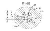
第2H圖係為包括分離電極165的局部橫截面圖與面板225的底視圖的蓋組件200的一部分的底視圖。如第2H圖所示,如上所述,分離電極165係設置成通過面板225的一部分,並包括導電桿166與電極屏蔽168。在一些實施例中,屏蔽間隙278係形成於導電桿166與電極屏蔽168之間。通常期望最小化屏蔽間隙278的大小,以改善導電桿166在處理期間與處理區域110的電容耦接。然而,在一些配置中,屏蔽間隙278可以設計為在0.01mm與1mm之間。此外,在分離電極165的表面與穿孔面板225及下板210的相鄰表面之間形成真空間隙276。真空間隙276係為不包含材料的區域(例如,包含真空的區域),而形成於每一分離電極165的外邊緣(例如,電極屏蔽168的外表面)與穿孔面板225及下板210的相鄰定位表面之間。在一個實例中,相鄰表面可以包括具有內邊緣229的通孔,內邊緣229係與分離電極165的外表面間隔開等於真空間隙276的距離279。真空間隙276的大小通常使得在處理期間不會在其間形成的空間中形成電漿,並且可以在0.1mm與1mm之間(例如,在約0.1與約0.25mm之間)。FIG. 2H is a bottom view of a portion of lid assembly 200 including a partial cross-sectional view of separate electrode 165 and a bottom view of panel 225 . As shown in FIG. 2H , as mentioned above, the separate electrode 165 is disposed through a portion of the panel 225 and includes the conductive rod 166 and the electrode shield 168 . In some embodiments, a shield gap 278 is formed between the conductive rod 166 and the electrode shield 168 . It is generally desirable to minimize the size of the shield gap 278 to improve the capacitive coupling of the conductive rods 166 to the processing region 110 during processing. However, in some configurations, shield gap 278 may be designed to be between 0.01 mm and 1 mm. In addition, a vacuum gap 276 is formed between the surface of the separated electrode 165 and adjacent surfaces of the perforated panel 225 and the lower plate 210 . Vacuum gap 276 is a region that does not contain material (eg, a region that contains a vacuum) and is formed between the outer edge of each separated electrode 165 (eg, the outer surface of electrode shield 168 ) and the perforated face plate 225 and lower plate 210. between adjacent positioning surfaces. In one example, the adjacent surface may include a through hole having an inner edge 229 spaced from the outer surface of the separated electrode 165 by a distance 279 equal to the vacuum gap 276 . Vacuum gap 276 is typically sized such that no plasma forms in the space formed therebetween during processing, and may be between 0.1 mm and 1 mm (eg, between about 0.1 and about 0.25 mm).

如第2G圖所示,分離電極165係跨越XY平面(例如,平行於蓋組件200的表面226)設置成所期望的圖案。參考電極元件225A(亦即,交叉影線區域)亦以所期望的圖案設置於圍繞分離電極165中之每一者,並在分離電極165中之每一者之間,以針對由RF源組件150提供到分離電極165中之每一者的RF功率提供對稱及可靠的接地路徑。如第2G圖及第2H圖所示,參考電極元件225A的至少一部分係圍繞分離電極165中之每一者。與暴露至處理區域的每一分離電極165的暴露的尖端表面區域相關聯的總區域可以定義為電極表面區域A1,而參考電極元件225A的交叉影線區域可以定義為總參考電極表面區域A2。當在具有對稱配置的處理區域110的處理腔室配置中使用,並且亦在具有定義部件(例如,腔室襯墊107)及/或腔室壁的非對稱配置的處理區域110的處理腔室配置使用時,對於控制電漿均勻性、電漿密度、或電漿離子能量而言,在分離電極表面區域A1與參考電極表面區域A2之間具有確定比率的對稱且可靠的接地路徑會是重要的。As shown in FIG. 2G, the separate electrodes 165 are arranged in a desired pattern across the XY plane (eg, parallel to the surface 226 of the lid assembly 200). Reference electrode elements 225A (i.e., cross-hatched regions) are also disposed in a desired pattern around and between each of the split electrodes 165 for reference to the RF source components provided by the RF source components. The RF power provided by 150 to each of split electrodes 165 provides a symmetrical and reliable path to ground. As shown in FIGS. 2G and 2H , at least a portion of reference electrode element 225A surrounds each of split electrodes 165 . The total area associated with the exposed tip surface area of each separate electrode 165 exposed to the processing area may be defined as electrode surface area A1 , while the cross-hatched area of reference electrode element 225A may be defined as total reference electrode surface area A2. When used in a processing chamber configuration having a symmetrically configured processing region 110, and also in a processing chamber having an asymmetrically configured processing region 110 defining components (e.g., chamber liners 107) and/or chamber walls When configured for use, a symmetrical and reliable ground path with a defined ratio between the split electrode surface area A1 and the reference electrode surface area A2 can be important for controlling plasma uniformity, plasma density, or plasma ion energy of.

在每一分離電極165與參考電極元件225A之間形成電極間隙287。電極間隙287係由參考電極元件225A的邊緣288與分離電極165的一部分之間形成的距離286所定義。空間或距離286係由分離電極165的一部分與參考電極元件225A的邊緣288之間產生的最小距離所定義。在一些配置中,中介的半導電及/或介電材料以及包含真空的區域(例如,真空間隙276)可以設置於電極間隙287內。參照第2G圖及第2H圖,在使用電極屏蔽168的一些實施例中,電極間隙287係形成於分離電極165的電極屏蔽168的外邊緣與邊緣288之間,或者取決於蓋組件200內的分離電極165的插入長度211,電極間隙287可以形成於從電極屏蔽168的屏蔽尖端168A(第2B圖)到邊緣288。如第2H圖所示,電極間隙287具有在電極屏蔽168的外邊緣與邊緣288之間所形成的距離286,距離286不同於面板225的邊緣299與電極屏蔽168之間所形成的真空間隙276的距離279。在替代配置中,電極間隙287的距離286可以相同於分離電極165與面板225的邊緣299(未圖示)之間的真空間隙276的距離279。在一些實施例中,距離286係在約0.5mm和與10mm之間(例如,在約1mm與約5mm之間)。在一個實例中,當在處理腔室中執行通常在接近10Torr的壓力下運行的電漿處理時,由電極間隙287提供的距離286係設定為約3mm,而當電漿處理為通常在接近1Torr的壓力下運行時,則設定為約10mm。儘管第2G圖係以正方形或矩形圖案圖示分離電極165的圖案與氣體遞送開口282的散佈圖案,但是因為可以使用分離電極165及/或開口282的任何其他期望的圖案(例如,徑向圖案或六邊形圖案),所以此配置並非意欲限制本文提供的本揭示的範圍。An electrode gap 287 is formed between each split electrode 165 and the reference electrode element 225A. Electrode gap 287 is defined by distance 286 formed between edge 288 of reference electrode element 225A and a portion of separate electrode 165 . Space or distance 286 is defined by the smallest distance created between a portion of split electrode 165 and edge 288 of reference electrode element 225A. In some configurations, an intervening semiconductive and/or dielectric material and a vacuum-containing region (eg, vacuum gap 276 ) may be disposed within electrode gap 287 . Referring to FIGS. 2G and 2H , in some embodiments using electrode shield 168 , electrode gap 287 is formed between the outer edge of electrode shield 168 separating electrode 165 and edge 288 , or depending on the inner edge of lid assembly 200 . Separating the insertion length 211 of the electrode 165 , an electrode gap 287 may be formed from the shield tip 168A ( FIG. 2B ) to the edge 288 of the electrode shield 168 . As shown in FIG. 2H, electrode gap 287 has a distance 286 formed between the outer edge of electrode shield 168 and edge 288 that is different from vacuum gap 276 formed between edge 299 of panel 225 and electrode shield 168. The distance is 279. In an alternative configuration, the distance 286 of the electrode gap 287 may be the same as the distance 279 of the vacuum gap 276 between the separating electrode 165 and the edge 299 (not shown) of the panel 225 . In some embodiments, distance 286 is between about 0.5 mm and 10 mm (eg, between about 1 mm and about 5 mm). In one example, the distance 286 provided by the electrode gap 287 is set to about 3 mm when performing plasma processing in a processing chamber operating at a pressure typically near 10 Torr, and when the plasma processing is typically operating at a pressure near 1 Torr. When running under the pressure, set it to about 10mm. Although FIG. 2G illustrates the pattern of split electrodes 165 and the dispersed pattern of gas delivery openings 282 in a square or rectangular pattern, any other desired pattern of split electrodes 165 and/or openings 282 (e.g., a radial pattern) may be used. or hexagonal pattern), so this configuration is not intended to limit the scope of the disclosure provided herein.

第2I圖係為第2B圖所示的分離電極165的一部分的示意性側剖面圖,為清楚起見,移除蓋組件200的一部分。如第2I圖所示,分離電極165中之每一者包括附接到功率分佈元件161的導電桿166。導電桿166插入電極屏蔽168中,電極屏蔽168圍繞導電桿166的下部,並設計成將導電桿166與處理腔室100的處理區域110(第1A圖及第2A圖)物理分離。導電桿166及電極屏蔽168係定位成通過參考電極元件225A中的開口,而使得導電桿及/或電極屏蔽的部分處於影響處理區域110中所形成的電漿的位置。如第2I圖所示,暴露於處理腔室的處理區域並位於參考電極元件225A下方的電極屏蔽尖端168A的外表面部分具有表面區域A1,而參考電極元件225A具有面向處理區域的表面區域A2。已經發現,分離電極165的表面區域A1的總和與參考電極元件表面區域A2的比率可以影響處理期間的電漿密度、電漿均勻性、或電漿離子能量。在操作中,存在可以改變區域A1與A2之間的比率的許多方法。在一個實例中,可以藉由確定分離電極的定位成通過參考電極元件225A中的孔洞並暴露於處理區域的部分的插入長度211(第2B圖)來控制區域A1。暴露於處理區域的分離電極165中之每一者的部分越大,則區域A1相對於A2越大。可以藉由選擇具有所期望厚度(例如,Z方向上的厚度)的下板210或藉由選擇具有所期望長度的導電桿與電極屏蔽來實現控制分離電極165中之每一者的暴露於處理區域的插入長度211(第2B圖)。此外,參考電極元件的表面區域A2可經調整及配置,以實現區域A1與A2之間的期望比率。FIG. 2I is a schematic side cross-sectional view of a portion of the split electrode 165 shown in FIG. 2B with a portion of the cap assembly 200 removed for clarity. As shown in FIG. 21 , each of the split electrodes 165 includes a conductive rod 166 attached to the power distribution element 161 . Conductive rods 166 are inserted into electrode shields 168 that surround the lower portion of conductive rods 166 and are designed to physically separate conductive rods 166 from processing region 110 of processing chamber 100 (FIGS. 1A and 2A). Conductive rod 166 and electrode shield 168 are positioned through openings in reference electrode element 225A such that portions of the conductive rod and/or electrode shield are positioned to affect the plasma formed in processing region 110 . As shown in FIG. 21 , the portion of the outer surface of electrode shield tip 168A exposed to the processing region of the processing chamber and positioned below reference electrode element 225A has surface area A1 , while reference electrode element 225A has surface area A2 facing the processing region. It has been found that the ratio of the sum of the surface areas A1 of the split electrodes 165 to the reference electrode element surface area A2 can affect the plasma density, plasma uniformity, or plasma ion energy during processing. In operation, there are many ways in which the ratio between areas A1 and A2 can be changed. In one example, the area A1 can be controlled by determining the insertion length 211 (FIG. 2B) of the portion of the split electrode positioned through the hole in the reference electrode element 225A and exposed to the treatment area. The larger the portion of each of the separate electrodes 165 exposed to the processing area, the larger the area A1 relative to A2. Controlling the exposure of each of the split electrodes 165 to the process can be achieved by selecting the lower plate 210 with a desired thickness (e.g., thickness in the Z direction) or by selecting conductive rods and electrode shields with a desired length. The insertion length of the region 211 (Fig. 2B). Furthermore, the surface area A2 of the reference electrode element can be adjusted and configured to achieve a desired ratio between areas A1 and A2.

第2J圖係為可以用於控制區域A1與區域A2之間的區域比率的分離電極165的另一實施例的橫截面圖。在一個配置中,分離電極165包括具有橫向配置的尖端部分273的電極屏蔽168,尖端部分273比第2I圖所示的電極屏蔽168的電極屏蔽尖端168A部分的配置更寬。電極屏蔽168包括側壁272、平坦底部尖端部分273、及具有內側壁276與內底部表面275的內部部分274。導電桿166係附接到具有所期望的形狀及大小(例如,表面區域)的導電尖端290或由導電尖端290形成。導電尖端290通常由於其形狀及分離電極165內的位置以及相對於參考電極元件225A的位置,而配置成藉由期望地分佈處理期間而建立的所產生電場,以在處理區域110內產生所期望的局部電漿均勻性及電漿密度。在一個配置中,導電尖端290具有比導電桿166更大的橫向區域(亦即,第2H圖所示的XY平面)。導電尖端290可以由金屬(例如,銅、鋁、鎳、銀、鈦、或其合金)或其他有用的導電材料形成。在一個實施例中,導電尖端290可以由與導電桿166相同的導電材料形成。在一個實施例中,導電尖端290由不同於導電桿166的導電材料形成。FIG. 2J is a cross-sectional view of another embodiment of a split electrode 165 that can be used to control the area ratio between area A1 and area A2. In one configuration, the split electrode 165 includes an electrode shield 168 having a laterally configured tip portion 273 that is wider than the configuration of the electrode shield tip 168A portion of the electrode shield 168 shown in FIG. 21 . The electrode shield 168 includes sidewalls 272 , a flat bottom tip portion 273 , and an inner portion 274 having an inner sidewall 276 and an inner bottom surface 275 . The conductive rod 166 is attached to or formed from a conductive tip 290 having a desired shape and size (eg, surface area). Conductive tip 290 is generally configured, due to its shape and location within separate electrode 165 and relative to reference electrode element 225A, to produce a desired electric field within processing region 110 by desirably distributing the generated electric field established during processing. local plasma uniformity and plasma density. In one configuration, the conductive tip 290 has a larger lateral area (ie, the XY plane shown in FIG. 2H ) than the conductive rod 166 . Conductive tip 290 may be formed from metal (eg, copper, aluminum, nickel, silver, titanium, or alloys thereof) or other useful conductive material. In one embodiment, conductive tip 290 may be formed from the same conductive material as conductive rod 166 . In one embodiment, conductive tip 290 is formed of a different conductive material than conductive rod 166 .

在一些實施例中,為了確保導電桿166及導電尖端290具有與電極屏蔽168及蓋組件200一致的關係,提供彈簧組件280,以將壓力施加至導電桿166與導電尖端290,而使得導電尖端290至少與電極屏蔽168的尖端部分273的內底部表面275接觸。在一些實施例中,電極屏蔽168包括放置於下板210的表面上的上屏蔽部分271,以可靠地固定內底部表面275相對於參考電極元件225A的位置。在一個配置中,如第2B圖所示,電極屏蔽的上屏蔽部分271係放置於O形環169上,O形環169係放置於下板210的表面上。因此,彈簧組件280、導電桿166、導電尖端290、電極屏蔽168、及下板210的支撐表面的位置的配置係用於提供導電尖端290相對於參考電極元件225A與處理腔室的處理區域110的一致定向及位置(例如,Z方向)。In some embodiments, to ensure that the conductive rod 166 and the conductive tip 290 have a consistent relationship with the electrode shield 168 and the cover assembly 200, a spring assembly 280 is provided to apply pressure to the conductive rod 166 and the conductive tip 290 such that the conductive tip 290 is in contact with at least the inner bottom surface 275 of the tip portion 273 of the electrode shield 168 . In some embodiments, the electrode shield 168 includes an upper shield portion 271 placed on the surface of the lower plate 210 to securely fix the position of the inner bottom surface 275 relative to the reference electrode element 225A. In one configuration, as shown in FIG. 2B , the upper shield portion 271 of the electrode shield is placed on the O-ring 169 which is placed on the surface of the lower plate 210 . Accordingly, the configuration of the position of the spring assembly 280, the conductive rod 166, the conductive tip 290, the electrode shield 168, and the support surface of the lower plate 210 is to provide the relative relation of the conductive tip 290 to the reference electrode element 225A and the processing region 110 of the processing chamber. Consistent orientation and position (for example, Z direction) of .

第2K圖係為第2J圖所示的導電尖端290的特寫圖示。導電桿166係裝配在電極導電尖端290的插座294內。下彎曲區域292提供具有將下表面291連接到側壁293的「彎曲邊緣」或成形邊緣295的暴露邊緣區域。與成形邊緣295組合的下表面291提供包括導電尖端290處的寬的平坦接觸表面的所期望的電極形狀。平坦接觸表面可以用於維持跨越電極屏蔽168的平坦的內底部表面275上的牢固且均勻的接觸,而藉此確保跨越具有相同或類似風格的導電尖端290的蓋組件200分佈的導電桿166與導電尖端290的一致長度。Figure 2K is a close-up illustration of the conductive tip 290 shown in Figure 2J. Conductive rod 166 fits within socket 294 of electrode conductive tip 290 . Lower curved region 292 provides an exposed edge region with a “curved edge” or shaped edge 295 connecting lower surface 291 to sidewall 293 . The lower surface 291 in combination with the shaped edge 295 provides the desired electrode shape including a wide flat contact surface at the conductive tip 290 . The flat contact surface can be used to maintain firm and uniform contact across the flat inner bottom surface 275 of the electrode shield 168, thereby ensuring that the conductive rods 166 distributed across the cover assembly 200 having the same or similar style of conductive tips 290 are in contact with The consistent length of the conductive tip 290.

第2L圖係為導電尖端290的替代實施例的特寫圖示。在此實施例中,導電尖端290具有下表面291,下表面291具有連接到導電尖端290的側壁293的非平坦或彎曲的形狀。下表面291的彎曲形狀可以是半球形、圓錐形(未圖示)、或任何其他彎曲輪廓。當RF偏壓時,下表面291的彎曲形狀可以提供所期望的場形狀及/或與電極屏蔽168的內底部表面275的一致接觸點(例如,配合平坦表面以避免平行度問題),而在使用相同風格的導電尖端290時,藉此確保跨越蓋組件200的導電桿166與導電尖端290的一致長度。FIG. 2L is a close-up illustration of an alternate embodiment of a conductive tip 290 . In this embodiment, the conductive tip 290 has a lower surface 291 having a non-planar or curved shape connected to a sidewall 293 of the conductive tip 290 . The curved shape of the lower surface 291 may be hemispherical, conical (not shown), or any other curved profile. The curved shape of the lower surface 291 may provide a desired field shape and/or a consistent point of contact with the inner bottom surface 275 of the electrode shield 168 when RF biased (e.g., mating with a flat surface to avoid parallelism issues), while at Using the same style of conductive tip 290 thereby ensures a consistent length of conductive rod 166 and conductive tip 290 across cover assembly 200 .

第2M圖係為如第2J圖所示的導電尖端290的另一替代實施例的特寫圖示。在此實施例中,導電尖端290具有T形配置,而具有下表面291、成形邊緣295、下側壁296、成形上區域297、及連接區域298。連接區域298將成形上區域297連接到上側壁293。與成形邊緣295組合的下表面291提供接觸表面,而可以允許導電尖端290維持跨越電極屏蔽168的平坦內底部表面275的牢固且均勻的接觸,而當使用相同風格的導電尖端時,藉此確保跨越蓋組件200的導電桿166與導電尖端290的一致長度。儘管未圖示於第2M圖中,但是在一些實施例中,下表面291可以具有彎曲形狀(例如,凸起或凹陷形狀),以在RF偏壓時,提供所期望的場形狀及/或與電極屏蔽168的內底部表面275的一致接觸點或線。FIG. 2M is a close-up illustration of another alternative embodiment of the conductive tip 290 shown in FIG. 2J. In this embodiment, the conductive tip 290 has a T-shaped configuration with a lower surface 291 , a shaped edge 295 , a lower sidewall 296 , a shaped upper region 297 , and a connection region 298 . Connection region 298 connects shaped upper region 297 to upper sidewall 293 . The lower surface 291 in combination with the shaped edge 295 provides a contact surface that may allow the conductive tip 290 to maintain a firm and uniform contact across the flat inner bottom surface 275 of the electrode shield 168, thereby ensuring that when the same style of conductive tip is used, A consistent length of the conductive rod 166 and the conductive tip 290 spans the cover assembly 200 . Although not shown in FIG. 2M, in some embodiments, the lower surface 291 may have a curved shape (e.g., a convex or concave shape) to provide a desired field shape and/or A consistent point or line of contact with the inner bottom surface 275 of the electrode shield 168 .

第2N圖圖示第2G圖所示的參考電極元件與分離電極陣列的關係的替代實施例的底視圖。第2N圖描繪分離電極165的陣列,其中分離電極165的總暴露表面區域的關係或分離電極165的電極表面區域A1的總和係與參考電極元件225A的表面區域A2大致相同。區域A1與A2並不包括形成於分離電極165的邊緣與參考電極元件225A的邊緣288之間的電極間隙287。可以調整跨越圍繞分離電極165的電極間隙287的距離286,以控制所形成的電漿的性質及/或調整參考電極元件225A的區域A2。已經發現,當使用分離電極165的總區域或分離電極165的區域A1的總和係與面向處理區域的參考電極元件225A的側表面區域(例如,平行於第2A圖及第2N圖所示的XY平面)的區域A2相同的配置時,電漿密度與電漿均勻性的一致性增加。在一個實例中,電極表面區域A1的總和與面向處理區域的表面區域A2的比率係在0.8:1與1.2:1的比率之間。在另一實例中,表面區域A1的總和與面向處理區域的表面區域A2的比率係在0.9:1與1.1:1之間。Figure 2N illustrates a bottom view of an alternative embodiment of the relationship of the reference electrode element to the array of split electrodes shown in Figure 2G. FIG. 2N depicts an array of split electrodes 165 in which the relationship of the total exposed surface area of split electrodes 165, or the sum of electrode surface areas A1 of split electrodes 165, is substantially the same as surface area A2 of reference electrode element 225A. Areas A1 and A2 do not include the electrode gap 287 formed between the edge of the split electrode 165 and the edge 288 of the reference electrode element 225A. The distance 286 across the electrode gap 287 surrounding the split electrode 165 can be adjusted to control the properties of the plasma formed and/or to adjust the area A2 of the reference electrode element 225A. It has been found that when using the total area of the split electrode 165 or the sum of the area A1 of the split electrode 165 is the same as the side surface area of the reference electrode element 225A facing the treatment area (e.g., parallel to the XY shown in Figures 2A and 2N). When the configuration of the area A2 of the plane) is the same, the consistency of the plasma density and the plasma uniformity increases. In one example, the ratio of the sum of the electrode surface areas A1 to the surface area A2 facing the treatment area is between a ratio of 0.8:1 and 1.2:1. In another example, the ratio of the sum of the surface areas A1 to the surface area A2 facing the treatment area is between 0.9:1 and 1.1:1.

返回參照第2A圖,在一些實施例中,熱控制導管250A與250B可操作地耦接到溫度控制系統(未圖示)。溫度控制系統包括與系統控制器50通訊的溫度控制器(未圖示)。系統控制器50通常係設計成促進處理腔室100的控制及自動化,並且可以與各種感測器、致動器、及相關聯於處理腔室100的其他裝備通訊。系統控制器50通常包括中央處理單元(CPU)(未圖示)、記憶體(未圖示)、及支援電路(或I/O)(未圖示)。CPU可以是工業設定中用於控制各種系統功能、基板移動、腔室處理、及控制支援硬體(例如,感測器、內部及外部機器人、馬達、氣體流量控制等)的任何形式的電腦處理器中之一者,並且可監測系統中所執行的處理(例如,RF功率測量、腔室處理時間、I/O訊號等)。記憶體係連接至CPU,並且可以是電腦可讀取媒體,可以是例如隨機存取記憶體(RAM)、唯讀記憶體(ROM)、軟碟、硬碟、或任何其他形式的數位儲存的本端或遠端的容易取得的記憶體中之一或更多者。可以將軟體指令及資料編碼並儲存於記憶體中,以指示CPU。支援電路亦連接至CPU,以藉由習知方式支援處理器。支援電路可以包括快取記憶體、功率供應器、時脈電路、輸入/輸出電路,子系統、及類似者。可藉由系統控制器50讀取的程式(或電腦指令)確定哪些任務可在處理腔室100中的基板上執行。較佳地,程式係為可藉由系統控制器50讀取的軟體,並包括用於執行與監測、執行、及控制基板的移動、支撐、及/或定位相關的任務的代碼,以及在處理腔室100中執行的各種處理配方任務及各種腔室處理配方操作的代碼。Referring back to FIG. 2A , in some embodiments, thermal control conduits 250A and 250B are operatively coupled to a temperature control system (not shown). The temperature control system includes a temperature controller (not shown) in communication with the system controller 50 . System controller 50 is generally designed to facilitate the control and automation of processing chamber 100 and may communicate with various sensors, actuators, and other equipment associated with processing chamber 100 . The system controller 50 generally includes a central processing unit (CPU) (not shown), a memory (not shown), and supporting circuits (or I/O) (not shown). A CPU may be any form of computer processing used in an industrial setting to control various system functions, substrate movement, chamber processing, and control support hardware (e.g., sensors, internal and external robots, motors, gas flow control, etc.) One of the devices, and can monitor the processing performed in the system (eg, RF power measurement, chamber processing time, I/O signals, etc.). The memory system is connected to the CPU and can be a computer readable medium such as random access memory (RAM), read only memory (ROM), floppy disk, hard disk, or any other form of digital storage One or more of the easily accessible memories at the end or at the remote end. Software instructions and data can be encoded and stored in the memory to instruct the CPU. Support circuitry is also coupled to the CPU to support the processor in conventional manner. Support circuits may include cache memory, power supplies, clock circuits, input/output circuits, subsystems, and the like. Programs (or computer instructions) readable by the system controller 50 determine which tasks can be performed on substrates in the processing chamber 100 . Preferably, the program is software readable by the system controller 50 and includes code for performing tasks related to monitoring, executing, and controlling the movement, support, and/or positioning of the substrate, and during processing Codes for various process recipe tasks executed in chamber 100 and various chamber process recipe operations.

溫度控制系統可以包括與溫度控制器通訊的溫度感測器。溫度感測器可以定位於主體201內,以監測蓋組件200的主體201的溫度。在一些實施例中,腔室主體105包括耦接到溫度控制器的溫度控制導管。溫度控制器可以包括伺服控制器,而控制連到電阻加熱器的電功率,以及流體控制連到熱控制導管250A的流體。在操作中,可以依據來自溫度感測器中之一或更多者的反饋,而藉由系統控制器50將蓋組件200的設定點溫度提供到溫度控制器。溫度控制系統的實施例可以用於在電漿打開狀態及電漿關閉狀態之間的循環期間提供蓋組件200的均勻溫度。處理設定點溫度的維持可以在單一基板處理以及基板對基板處理中產生更穩定的處理結果。以此方式,可靠地控制蓋組件200的溫度控制及處理溫度。如本文所述的溫度控制系統的實施例可以用於維持約攝氏120度至約攝氏160度的設定點溫度。The temperature control system may include a temperature sensor in communication with the temperature controller. A temperature sensor may be positioned within the body 201 to monitor the temperature of the body 201 of the cap assembly 200 . In some embodiments, chamber body 105 includes a temperature control conduit coupled to a temperature controller. The temperature controller may include a servo controller to control the electrical power to the resistive heater, and a fluid control to the fluid to the thermal control conduit 250A. In operation, the set point temperature of the lid assembly 200 may be provided to the temperature controller by the system controller 50 based on feedback from one or more of the temperature sensors. Embodiments of a temperature control system may be used to provide a uniform temperature of the lid assembly 200 during cycling between the plasma-on state and the plasma-off state. Maintenance of the process set point temperature can produce more stable process results in single substrate processing as well as substrate-to-substrate processing. In this way, the temperature control and processing temperature of the lid assembly 200 is reliably controlled. Embodiments of the temperature control system as described herein may be used to maintain a set point temperature of about 120 degrees Celsius to about 160 degrees Celsius.

返回參照第1A圖至第1B圖,下腔室組件30包括腔室主體105與支撐組件115。支撐組件115可以包括電極464,而可以藉由使用支撐RF源組件460來偏壓。支撐RF源組件460包括RF功率供應器461與RF匹配462,而經配置以將RF頻率以約50kHz與200MHz之間(例如,約13.56MHz與約162MHz之間,或者甚至約50MHz與約162MHz之間)的頻率提供到電極464。支撐RF源組件460亦可以包括切換裝置469,而設置於電極464與RF功率供應器461之間(例如,電極464與RF匹配462之間)。切換裝置469可以包括RF同軸真空中繼器,而在打開狀態時具有高阻抗,並在關閉狀態下具有低阻抗,如下面進一步所討論。因此,電極464可以與分離電極165一起使用,以在處理區域110中形成電漿。可以調整供應到電極464的RF功率、相對於分離電極165的基板112的位置、及/或提供到分離電極165的RF功率,以控制所形成的電漿(例如,自由基及/或離子相互作用的量)與基板112的暴露表面的相互作用。支撐組件115可以是真空卡盤、靜電卡盤、或其他類型的基板支撐件(可以由導熱材料製成(例如,鋁或氮化鋁))。Referring back to FIGS. 1A-1B , the lower chamber assembly 30 includes a chamber body 105 and a support assembly 115 . The support assembly 115 may include electrodes 464 that may be biased using the support RF source assembly 460 . The supporting RF source assembly 460 includes an RF power supply 461 and an RF match 462 configured to drive RF frequencies between about 50 kHz and 200 MHz (e.g., between about 13.56 MHz and about 162 MHz, or even between about 50 MHz and about 162 MHz) Between) frequencies are provided to electrodes 464. The supporting RF source assembly 460 may also include a switching device 469 disposed between the electrode 464 and the RF power supply 461 (eg, between the electrode 464 and the RF match 462 ). Switching device 469 may comprise an RF coaxial vacuum repeater with a high impedance in an on state and a low impedance in an off state, as discussed further below. Accordingly, electrode 464 may be used with split electrode 165 to form a plasma in treatment region 110 . The RF power supplied to electrode 464, the position of substrate 112 relative to split electrode 165, and/or the RF power supplied to split electrode 165 can be adjusted to control the resulting plasma (e.g., free radical and/or ion interaction). The amount of action) interacts with the exposed surface of the substrate 112. Support assembly 115 may be a vacuum chuck, electrostatic chuck, or other type of substrate support (which may be made of a thermally conductive material (eg, aluminum or aluminum nitride)).

腔室主體105包括腔室襯墊107,而經配置以將處理區域110與下腔室區域430分離。腔室主體105包括複數個腔室側壁405與腔室底板410,而可由一或更多種處理兼容材料形成(例如,鋁、陽極氧化鋁、鍍鎳鋁、鍍鎳鋁6061-T6、不銹鋼、及其組合與合金)。複數個腔室側壁405與腔室底板410經配置以支撐容納於上腔室組件20內的部件中之一或更多者,並藉由使用泵440而允許在處理區域110、下腔室區域430、及排空區域411內維持所期望的壓力。在一個實例中,泵440包括渦輪泵及/或機械泵,而能夠在處理區域110、下腔室區域430、及排空區域411內產生真空壓力。在一個處理實例中,在基板112的電漿處理期間,在處理區域110內將真空壓力維持成約10mTorr與10Torr之間(例如,約100mTorr與10Torr之間)的壓力。The chamber body 105 includes a chamber liner 107 configured to separate the processing region 110 from the lower chamber region 430 . The chamber body 105 includes a plurality of chamber sidewalls 405 and a chamber floor 410, and may be formed from one or more process compatible materials (e.g., aluminum, anodized aluminum, nickel-plated aluminum, nickel-plated aluminum 6061-T6, stainless steel, and their combinations and alloys). The plurality of chamber sidewalls 405 and chamber floor 410 are configured to support one or more of the components housed within the upper chamber assembly 20 and, by use of the pump 440, to allow 430, and the desired pressure is maintained within the evacuated region 411. In one example, the pump 440 includes a turbo pump and/or a mechanical pump capable of generating vacuum pressure within the processing region 110 , the lower chamber region 430 , and the evacuation region 411 . In one processing example, a vacuum pressure is maintained within processing region 110 at a pressure between about 10 mTorr and 10 Torr (eg, between about 100 mTorr and 10 Torr) during plasma processing of substrate 112 .

腔室主體105亦包括形成在側壁405中之一者中的裝載埠(未圖示)。然後,藉由狹縫閥(未圖示)選擇性打開及關閉裝載埠,以允許藉由基板處理機器人(未圖示)進出腔室主體105的內部。可以透過裝載埠將基板112轉移進及轉移出處理腔室100,裝載埠係連到處理腔室100所設置的相鄰轉移腔室(未圖示)及/或裝載鎖定腔室,或者連到處理腔室100所在的群集工具內的另一腔室。支撐組件115可以相對於腔室主體105移動。基板112可以設置於支撐組件115的上表面130上,以進行處理。支撐組件115可以位於與裝載埠相鄰的位置,以用於基板轉移。支撐組件115亦可以移動到靠近蓋組件200的下表面126的位置,以進行處理。支撐組件115亦可以相對於腔室主體105旋轉。提升銷(未圖示)亦可以用於使基板112遠離支撐組件115的上表面130,以在基板轉移期間能夠與基板處理機器人進行交換。The chamber body 105 also includes a load port (not shown) formed in one of the side walls 405 . Then, the loading port is selectively opened and closed by a slit valve (not shown), so as to allow a substrate processing robot (not shown) to enter and exit the interior of the chamber body 105 . The substrate 112 may be transferred into and out of the processing chamber 100 through a load port connected to an adjacent transfer chamber (not shown) and/or a load lock chamber provided in the processing chamber 100, or connected to Another chamber within the cluster tool where processing chamber 100 is located. The support assembly 115 is movable relative to the chamber body 105 . The substrate 112 may be disposed on the upper surface 130 of the support assembly 115 for processing. The support assembly 115 may be located adjacent to the loadport for substrate transfer. The support assembly 115 can also be moved to a position adjacent to the lower surface 126 of the cover assembly 200 for processing. The support assembly 115 can also rotate relative to the chamber body 105 . Lift pins (not shown) may also be used to keep the substrate 112 away from the upper surface 130 of the support assembly 115 to enable exchange with the substrate handling robot during substrate transfer.

如第1A圖所示,側壁405與腔室底板410圍繞排空區域411。真空泵440係設置於腔室底板410中的真空泵開口410a中,並相對於側壁405的對稱軸線而位於中心。與支撐組件115同軸的容納壁415以及延伸於台座120與容納壁415之間的可撓波紋管417將支撐組件115圍繞於內部中央空間419中。中央空間419係與由真空泵440排空的包括排空區域411及處理區域110的容積隔離。參照第1B圖,存在三個中空徑向支柱420,並定義以120度間隔而隔開的徑向進出通路421,而延伸通過腔室主體側壁405,並提供對於中央空間419的進出。三個軸向排氣通路422係定義於三個徑向支柱420之間。可以透過不同的徑向進出通路421提供不同的用途,例如包括連接到電極464的RF功率電纜或剛性RF傳輸線132、連接到支撐組件115中的加熱器元件的加熱器電壓供應線、連接到電極464的靜電夾持電壓供應線、冷卻劑供應線、及用於工件支撐表面121中的背側氦氣通道的氦供應線。工件支撐提升致動器450係相對於腔室主體是固定的,並藉由使用機械致動器(未圖示)垂直(例如,Z方向)移動支撐組件115。因此,工件支撐提升致動器450可以用於藉由使用從系統控制器50接收的命令來控制電極對基板間隔213(第2B圖)。此距離的變化係改變所形成的電漿111內的電漿離子密度的分佈。提升致動器的移動可以用於改善跨越基板112的表面的處理(例如,蝕刻)速率的分佈均勻性。此距離的變化亦可用於改變電漿離子或電子密度相對於工件處的電漿自由基密度的比率。在一些實施例中,可期望在基板上執行電漿處理配方的不同部分期間調整電極對基板間隔213,而可以調整基板的表面暴露於形成於電漿中的離子及/或自由基的量。在一個實例中,可期望在第一處理步驟期間將基板的表面定位成更靠近分離電極165,以允許基板暴露於電漿中所產生的第一數量的離子,然後在第二處理步驟期間將基板的表面定位成距離分離電極165更遠的距離,以允許基板暴露於電漿中所產生的第二數量的離子。在此實例中,基板表面所暴露的第二數量的離子將小於基板表面在第一處理步驟期間所暴露的第一數量的離子。在另一實例中,藉由在處理期間切換處理步驟的順序,基板與分離電極165之間的間隔係與先前實例相反,以改變基板表面暴露於所產生的離子的量。舉例而言,提升致動器450可以藉由使用者透過系統控制器50來控制。As shown in FIG. 1A , sidewall 405 and chamber floor 410 surround evacuated region 411 . The vacuum pump 440 is disposed in the vacuum pump opening 410 a in the chamber floor 410 and is centrally located with respect to the axis of symmetry of the side wall 405 . The receiving wall 415 coaxial with the supporting assembly 115 and the flexible bellows 417 extending between the pedestal 120 and the receiving wall 415 surround the supporting assembly 115 in the inner central space 419 . The central space 419 is isolated from the volume including the evacuated area 411 and the processing area 110 which is evacuated by the vacuum pump 440 . Referring to FIG. 1B , there are three hollow radial struts 420 and define radial access passages 421 spaced at 120° intervals, extending through chamber body sidewall 405 and providing access to central volume 419 . Three axial exhaust passages 422 are defined between the three radial struts 420 . Different uses can be provided through different radial accesses 421, including for example RF power cables or rigid RF transmission lines 132 connected to electrodes 464, heater voltage supply lines connected to heater elements in support assembly 115, connections to electrode 464 electrostatic clamping voltage supply lines, coolant supply lines, and helium supply lines for the backside helium channels in the workpiece support surface 121. The workpiece support lift actuator 450 is fixed relative to the chamber body and moves the support assembly 115 vertically (eg, in the Z direction) by using a mechanical actuator (not shown). Accordingly, the workpiece support lift actuator 450 may be used to control the electrode-to-substrate spacing 213 by using commands received from the system controller 50 (FIG. 2B). Variation of this distance changes the distribution of plasma ion density within the formed plasma 111 . Movement of the lift actuator may be used to improve the uniformity of distribution of processing (eg, etching) rates across the surface of the substrate 112 . Variation of this distance can also be used to change the ratio of plasma ion or electron density relative to plasma radical density at the workpiece. In some embodiments, it may be desirable to adjust the electrode-to-substrate spacing 213 during execution of different portions of the plasma treatment recipe on the substrate, so that the amount of exposure of the substrate's surface to ions and/or free radicals formed in the plasma may be adjusted. In one example, it may be desirable to position the surface of the substrate closer to the separation electrode 165 during a first processing step to allow the substrate to be exposed to a first amount of ions generated in the plasma, and then during a second processing step to The surface of the substrate is positioned at a greater distance from the separation electrode 165 to allow exposure of the substrate to the second quantity of ions generated in the plasma. In this example, the second amount of ions to which the substrate surface is exposed will be less than the first amount of ions to which the substrate surface was exposed during the first processing step. In another example, by switching the order of the processing steps during the process, the spacing between the substrate and the split electrodes 165 is reversed from the previous example to vary the amount of exposure of the substrate surface to the generated ions. For example, lift actuator 450 may be controlled by the user through system controller 50 .

包括真空泵開口410a與軸向排氣通路422的軸向中心排氣組件避免跨越基板112的處理分佈的不對稱或歪斜。下環狀柵格107B遮蔽處理區域110,而免於徑向支柱420的不連續或影響。軸向中心排氣組件與接地板184下方的RF電流的對稱分佈的組合最小化整個處理區域110的歪斜效應,並增強處理區域110中的處理均勻性。The axial center exhaust assembly including the vacuum pump opening 410 a and the axial exhaust passage 422 avoids asymmetry or skewing of the process distribution across the substrate 112 . The lower annular grid 107B shields the treatment area 110 from the discontinuity or influence of the radial struts 420 . The combination of the axially centered exhaust assembly and the symmetrical distribution of the RF current below the ground plate 184 minimizes skew effects across the processing region 110 and enhances processing uniformity in the processing region 110 .

在一個實施例中,上腔室組件20包括磁體組件,磁體組件包括由磁體源177供電的電磁體176。磁體組件可以是環繞軸線對稱或尖點型磁體系統,而在處理腔室的邊緣處或中心建立具有峰值場的B場。可替代地,磁體組件可以包括「XY」線圈組件(例如,二或更多個線圈),而可以藉由使用透過在「XY」線圈組件中找到的所期望定向的線圈提供的電流的組合來提供跨越基板的表面而指向平行於基板的表面的任意方向的磁場。改變所產生的磁場的能力可以用於補償由電極組件160中所發現的部件形成的電漿中的不對稱性。改變所產生的磁場的能力亦可用於校正處理腔室中所處理的基板的性質中的任何不對稱性(例如,現有的厚度不均勻性),或者有意地在處理腔室中的基板上執行的處理結果中建立不對稱性,而預期在基板上執行的後續處理步驟中發現的處理結果的歪斜。磁體組件可以用於調諧電漿性質,以改變一或更多個處理變量(例如,蝕刻速率或沉積速率)。舉例而言,在高RF頻率(例如,162MHz)下,可以利用磁體來減少在基板112的中心附近發現的電漿密度的峰值。在一些實施例中,較低RF頻率(例如,約<60MHz)可能不需要磁體來調諧所產生的電漿。RF 功率遞送配置實例 In one embodiment, upper chamber assembly 20 includes a magnet assembly including an electromagnet 176 powered by a magnet source 177 . The magnet assembly can be a symmetric around axis or a cusp type magnet system, with the B field having a peak field established at the edge or center of the process chamber. Alternatively, the magnet assembly may comprise an "XY" coil assembly (e.g., two or more coils), which may be detected by using a combination of currents supplied through the coils in the desired orientation found in the "XY" coil assembly. A magnetic field is provided pointing in any direction parallel to the surface of the substrate across the surface of the substrate. The ability to vary the magnetic field generated may be used to compensate for asymmetries in the plasma formed by components found in electrode assembly 160 . The ability to vary the magnetic field generated can also be used to correct for any asymmetry in the properties of the substrate being processed in the processing chamber (e.g., existing thickness non-uniformity), or to intentionally perform Asymmetry is established in the processing results of the substrate, whereas skewing of the processing results found in subsequent processing steps performed on the substrate is expected. A magnet assembly can be used to tune plasma properties to vary one or more process variables (eg, etch rate or deposition rate). For example, at high RF frequencies (eg, 162 MHz), magnets can be utilized to reduce the peak of plasma density found near the center of the substrate 112 . In some embodiments, lower RF frequencies (eg, about <60 MHz) may not require magnets to tune the generated plasma. RF Power Delivery Configuration Example

第3A圖係為根據本文提供的本揭示的實施例的設置於蓋組件的電極組件160內的主RF功率遞送元件的橫截面圖。電極組件160包括透過功率分佈元件161耦接到導電桿166的連接元件154與中心連接元件155。導電桿166係配置為藉由使用RF源組件150中的RF功率產生部件而相對於參考電極(例如,參考電極元件225A或處理腔室壁(未圖示))而偏壓。在處理期間,從耦接到連接元件155的RF源提供RF電流「A」,而從耦接到連接元件154的RF源提供RF電流「B」。如下面進一步所討論,將功率提供到連接元件154與155的RF源可以是相同的RF源或不同的RF源。藉由控制透過連接元件154、155中之每一者遞送的RF功率的特性,以及藉由使用RF功率傳導元件的結構態樣(例如,功率分佈元件161與導電桿166),而可以控制提供到處理區域110的RF功率的均勻性以及因此產生的電漿111。在一些實施例中,電極組件160中的RF功率分佈部件的物理特性及/或連接元件154、155接觸功率分佈元件161的位置係經配置,並依據提供到電極組件內的不同功率遞送元件的RF功率之間產生的干擾,而使得由RF源所提供的RF功率具有所期望產生的波圖案。在一些實施例中,調整提供到連接元件154、155與功率分佈元件161的RF功率的電特性(例如,相角、頻率、功率),而使得由RF源所提供的RF功率能夠依據受驅動部件的阻抗、由電漿產生的負載、及在單獨提供到電極組件內的功率遞送元件的不同部分的RF功率之間產生的干擾,而實現所期望的波圖案以及前向RF功率訊號。FIG. 3A is a cross-sectional view of the primary RF power delivery element disposed within the electrode assembly 160 of the cap assembly, according to embodiments of the disclosure provided herein. The electrode assembly 160 includes a connection element 154 and a central connection element 155 coupled to a conductive rod 166 through a power distribution element 161 . Conductive rod 166 is configured to be biased relative to a reference electrode (eg, reference electrode element 225A or a process chamber wall (not shown)) by use of RF power generating components in RF source assembly 150 . During processing, RF current "A" is provided from an RF source coupled to connection element 155 , while RF current "B" is provided from an RF source coupled to connection element 154 . As discussed further below, the RF sources providing power to connection elements 154 and 155 may be the same RF source or different RF sources. By controlling the characteristics of the RF power delivered through each of the connecting elements 154, 155, and by using structural aspects of the RF power conducting elements (e.g., the power distribution element 161 and the conductive rod 166), it is possible to control the The uniformity of RF power to the treatment region 110 and thus the plasma 111 generated. In some embodiments, the physical characteristics of the RF power distribution components in the electrode assembly 160 and/or the locations where the connection elements 154, 155 contact the power distribution element 161 are configured and depend on the different power delivery elements provided into the electrode assembly. Interference between RF powers, so that the RF power provided by the RF source has the desired wave pattern. In some embodiments, the electrical characteristics (e.g., phase angle, frequency, power) of the RF power provided to the connection elements 154, 155 and the power distribution element 161 are adjusted such that the RF power provided by the RF source can be driven according to The impedance of the components, the loading caused by the plasma, and the resulting interference between the RF power supplied separately to different portions of the power delivery element within the electrode assembly achieve the desired wave pattern and forward RF power signal.

第3B圖係為設置於蓋組件的電極組件160內的主RF功率遞送元件的另一配置的橫截面圖。第3B圖所示的配置與第3A圖所示的配置的不同之處在於,可以在處理腔室100的製造期間,或者在藉由使用將連接元件的一端耦接到功率分佈元件161的一部分的連接組件330來將處理腔室安裝至場中時,調整連接元件(例如,第3A圖所示的連接元件155)的連接點363。在一個實施例中,連接組件330包括分佈板331,分佈板331包括複數個連接特徵332,複數個連接特徵332中之每一者係配置為接收導電連接元件341的一端,而導電連接元件341在相對端處耦接到功率分佈元件161的一部分。在一些配置中,可期望將導電連接元件341中之一或更多者定位至連接特徵332中,而使得一或更多個導電連接元件341距離功率分佈元件161的對稱位置(例如,功率分佈元件的中心點)一距離335。距離335或特徵332的間隔可經配置以最小化特定負載條件與驅動RF頻率的不均勻性。調整連接元件154、155與功率分佈元件161之間所形成的一或更多個連接點的物理位置的能力可以藉由改變在功率分佈元件161中形成的所產生波圖案,而用於補償及/或產生在處理區域110中形成的電漿中的所期望的不對稱性。Figure 3B is a cross-sectional view of another configuration of the primary RF power delivery element disposed within the electrode assembly 160 of the cap assembly. The configuration shown in FIG. 3B differs from the configuration shown in FIG. 3A in that it may be possible during manufacture of the processing chamber 100, or by using one end of the connection element to couple to a portion of the power distribution element 161 When installing the processing chamber into the field using the connection assembly 330, the connection point 363 of the connection element (eg, connection element 155 shown in FIG. 3A) is adjusted. In one embodiment, the connection assembly 330 includes a distribution plate 331 that includes a plurality of connection features 332, each of the plurality of connection features 332 is configured to receive one end of a conductive connection element 341, and the conductive connection element 341 Coupled at the opposite end to a portion of the power distribution element 161 . In some configurations, it may be desirable to position one or more of the conductive connection elements 341 into the connection feature 332 such that the one or more conductive connection elements 341 are located symmetrically from the power distribution element 161 (e.g., power distribution The center point of the component) a distance of 335. The distance 335 or the spacing of the features 332 can be configured to minimize non-uniformities in particular loading conditions and driving RF frequencies. The ability to adjust the physical location of one or more connection points formed between connection elements 154, 155 and power distribution element 161 can be used to compensate and and/or create a desired asymmetry in the plasma formed in the processing region 110 .

複數個分離電極165、功率分佈元件161、及參考電極225B係描繪為第4A圖至第4B圖、第5A圖至第5B圖、第6A圖至第6B圖、及第7A圖的加載傳輸線系統190,並在下面進一步描述。參考電極225B可以包括參考電極元件225A及/或接地處理腔室壁。在另一實施例中,如前所述,參考電極225B係由複數個分離電極的一部分形成,複數個分離電極係與參考電極元件225A分開接地。The plurality of split electrodes 165, power distribution element 161, and reference electrode 225B are depicted as loaded transmission line systems in FIGS. 4A-4B, 5A-5B, 6A-6B, and 7A. 190, and described further below. Reference electrode 225B may include reference electrode element 225A and/or a grounded process chamber wall. In another embodiment, as mentioned above, the reference electrode 225B is formed by a part of a plurality of separate electrodes, and the plurality of separate electrodes are grounded separately from the reference electrode element 225A.

第4A圖係為描繪用於驅動複數個分離電極165的RF源組件150的實施例的示意圖。RF遞送組件150包括RF產生器351、匹配網路355、及連接元件154、155。第3A圖的功率分佈元件161、複數個分離電極165、及參考接地係描繪為利用複數個阻抗365(示意性表示當在處理區域110中藉由將RF功率遞送到分離電極165而產生電漿時所產生的阻抗)加載的傳輸線系統190。複數個阻抗365通常是隨著驅動頻率下的RF功率的量而變化的複阻抗(Z f =R f +j XL f +XC f )) ),而相位係在處理區域110內形成電漿期間進行調整或變化。阻抗365通常包括電阻部件R、電感部件XL 、及電容部件XC 。接合部361使用連接元件154、155將匹配網路355的輸出連接到功率分佈元件161。為了簡化討論,在此實例中,所形成的電子電路包括二個連接元件154與一個連接元件155,然而,因為亦可以使用附加的連接元件154、155,所以此配置並非意欲限制本文提供的本揭示的範圍。因此,在此實例中,連接元件155將接合部361連接到功率分佈元件161的中心附近的連接點246(第2C1圖至第2C2圖)。第一連接元件154將接合部361連接到定位於功率分佈元件的一個邊緣(例如,功率分佈元件161的左邊緣)處的連接點247(第2C1圖至第2C2圖)。第二連接元件154將接合部361連接到定位於功率分佈元件的另一邊緣(例如,功率分佈元件161的右邊緣)處的連接點247(第2C1圖至第2C2圖)。在一些實施例中,選擇接合部361與連接點246、247中之每一者之間的距離,以隨著處理期間的驅動,在RF功率遞送部件中之每一者內實現所期望的波圖案。FIG. 4A is a schematic diagram depicting an embodiment of an RF source assembly 150 for driving a plurality of split electrodes 165 . The RF delivery component 150 includes an RF generator 351 , a matching network 355 , and connecting elements 154 , 155 . The power distribution element 161, the plurality of split electrodes 165, and the reference ground system of FIG. 3A are depicted as utilizing the plurality of impedances 365 (schematically representing when a plasma is generated in the processing region 110 by delivering RF power to the split electrodes 165). The resulting impedance) loads the transmission line system 190. The complex impedance 365 is typically a complex impedance that varies with the amount of RF power at the drive frequency ( Z ( f ) =R ( f ) +j ( XL ( f ) +XC ( f )) ), while the phase is tied at Adjustments or changes are made during the formation of the plasma within the processing region 110 . Impedance 365 generally includes a resistive component R, an inductive component X L , and a capacitive component X C . Junction 361 connects the output of matching network 355 to power distribution element 161 using connection elements 154 , 155 . To simplify the discussion, in this example the electronic circuit is formed to include two connection elements 154 and one connection element 155, however, this configuration is not intended to limit the present invention presented herein as additional connection elements 154, 155 may also be used. scope of disclosure. Thus, in this example, connection element 155 connects joint 361 to connection point 246 near the center of power distribution element 161 (Figs. 2C1-2C2). The first connection element 154 connects the junction 361 to the connection point 247 located at one edge of the power distribution element (eg, the left edge of the power distribution element 161 ) (Figs. 2C1-2C2). The second connection element 154 connects the junction 361 to the connection point 247 located at the other edge of the power distribution element (eg, the right edge of the power distribution element 161 ) (Figs. 2C1-2C2). In some embodiments, the distance between the junction 361 and each of the connection points 246, 247 is selected to achieve the desired waves within each of the RF power delivery components as actuated during processing. pattern.

通常,RF源組件150中的RF產生器係配置成將RF功率(電壓及/或電流)供應至電極組件160部件。RF產生器351的輸出阻抗經由匹配網路355與加載的傳輸線系統190的阻抗匹配,而有效地將功率從RF產生器351轉移到加載的傳輸線系統190。因此,匹配網路355係配置成依據在處理期間從RF產生器提供的驅動頻率來提供所期望的前向及反射RF功率。在一些實施例中,在約50千赫茲(kHz)與約3千兆赫茲(GHz)之間的範圍內提供由RF產生器提供的RF功率。已經發現,在以大於或等於13.56MHz的頻率下施加的RF功率(例如,在VHF範圍(30MHz至300MHz)或UHF範圍(300MHz至3GHz)中提供的RF功率)的配置中,本文描述的電極組件配置特別有用。相較於較低RF頻率所提供者,VHF或UHF範圍中的較高頻率RF功率有利地用於在較低的驅動電壓下提供更高的電漿密度。使用較低的驅動電壓對於防止或最小化電弧放電的風險是重要的,因為在使用CCP源配置時的電漿密度增加,所以電弧放電造成處理腔室中所處理的基板的損傷。使用較低的驅動電壓亦可以在所產生的電漿中提供降低的離子能量及/或較窄的離子能量分佈,而可以在處理形成於基板表面上的某些半導體裝置結構期間,提供改善的處理結果與減少的基板損傷。Typically, the RF generator in the RF source assembly 150 is configured to supply RF power (voltage and/or current) to the electrode assembly 160 components. The output impedance of the RF generator 351 is matched to the impedance of the loaded transmission line system 190 via the matching network 355 , effectively transferring power from the RF generator 351 to the loaded transmission line system 190 . Accordingly, matching network 355 is configured to provide the desired forward and reflected RF power depending on the drive frequency provided from the RF generator during processing. In some embodiments, the RF power provided by the RF generator is provided in a range between about 50 kilohertz (kHz) and about 3 gigahertz (GHz). It has been found that in configurations where RF power is applied at frequencies greater than or equal to 13.56 MHz (for example, RF power provided in the VHF range (30 MHz to 300 MHz) or the UHF range (300 MHz to 3 GHz) ), the electrodes described herein Component configuration is especially useful. Higher frequency RF power in the VHF or UHF range is advantageously used to provide higher plasma density at lower drive voltages than that provided by lower RF frequencies. The use of lower drive voltages is important to prevent or minimize the risk of arcing, which causes damage to substrates processed in the processing chamber due to the increased plasma density when using a CCP source configuration. The use of lower drive voltages can also provide reduced ion energy and/or narrower ion energy distribution in the generated plasma, which can provide improved Processing results with reduced substrate damage.

在操作期間,提供到連接點246、247中之每一者的RF功率造成RF波(電壓/及/或電流)在功率分佈元件161內從中心行進到邊緣,從邊緣行進到中心,以及從邊緣行進到邊緣。所傳輸的波係彼此相長及相消干涉,並在穩定狀態下在一些情況中可以在沿著功率分佈元件161以及沿著連接到功率分佈元件161的導電桿166的不同位置處產生具有峰值及谷值的駐波。在功率分佈元件161上以及沿著導電桿166的駐波的峰值與谷值的圖案係為電漿不均勻性與跨越蓋組件200的表面226的電漿密度的相對改變的重要因素。在一些應用中,藉由從單一源(例如,RF產生器351與匹配網路355)遞送RF功率而產生的干涉波圖案可以在導電桿166的尖端處提供可接受的功率分佈均勻性,而可以產生處理區域110內的可接受的電漿均勻性。然而,在其他應用中,電極組件160部件的物理配置可能不夠充分,因為波圖案的位置及振幅並不均勻,且不容易藉由調整遞送到電極組件160部件的RF功率的電特性或藉由物理電極組件160部件的更換及/或重新配置來改變。During operation, RF power supplied to each of the connection points 246, 247 causes RF waves (voltage and/or current) to travel within the power distribution element 161 from the center to the edge, from the edge to the center, and from the Edge to edge. The transmitted wave systems interfere constructively and destructively with each other and in steady state may in some cases produce peaks at different locations along the power distribution element 161 and along the conductive rod 166 connected to the power distribution element 161 and valley standing waves. The pattern of peaks and valleys of the standing wave on the power distribution element 161 and along the conductive rod 166 is an important factor in the relative change in plasma inhomogeneity and plasma density across the surface 226 of the lid assembly 200 . In some applications, the interferometric wave pattern generated by delivering RF power from a single source (e.g., RF generator 351 and matching network 355) may provide acceptable power distribution uniformity at the tip of conductive rod 166, while Acceptable plasma uniformity within the processing region 110 can be produced. In other applications, however, the physical configuration of the electrode assembly 160 components may not be sufficient because the wave pattern is not uniform in location and amplitude and cannot be easily adjusted by adjusting the electrical characteristics of the RF power delivered to the electrode assembly 160 components or by Physical electrode assembly 160 components can be changed by replacement and/or reconfiguration.

第4B圖係為描繪包括第4A圖所示的RF產生器351與附加RF產生器357的RF源組件150的實施例的示意圖。RF產生器351與RF產生器357都配置成將RF功率提供至匹配網路355、連接元件154、155、及電極組件160。在一個實施例中,RF產生器357係配置成以與由RF產生器351所提供的RF功率的頻率不同的頻率遞送RF功率。匹配網路355係配置成在由二個RF產生器所提供的二個不同的RF頻率提供匹配。在一些實施例中,由RF產生器351與RF產生器357所提供的RF功率的頻率差異顯著不同(例如,間隔數十或數百兆赫茲)。在一個實例中,RF產生器351係配置成以13.56 MHz提供RF功率,而RF產生器357係配置成以2MHz提供RF功率。在一個實施例中,RF產生器351係配置成以第一UHF或VHF頻率提供RF功率,而RF產生器357係配置成以低於VHF頻率的頻率提供RF功率。在一個實例中,RF產生器351係配置成以60MHz提供RF功率,而RF產生器357係配置成以2MHz提供RF功率。在另一實例中,RF產生器351係配置成以162MHz提供RF功率,而RF產生器357係配置成以13.56 MHz提供RF功率。FIG. 4B is a schematic diagram depicting an embodiment of RF source assembly 150 including RF generator 351 and additional RF generator 357 shown in FIG. 4A. Both the RF generator 351 and the RF generator 357 are configured to provide RF power to the matching network 355 , the connection elements 154 , 155 , and the electrode assembly 160 . In one embodiment, RF generator 357 is configured to deliver RF power at a different frequency than the RF power provided by RF generator 351 . Matching network 355 is configured to provide matching at two different RF frequencies provided by two RF generators. In some embodiments, the difference in frequency of the RF power provided by RF generator 351 and RF generator 357 is significantly different (eg, separated by tens or hundreds of megahertz). In one example, RF generator 351 is configured to provide RF power at 13.56 MHz, while RF generator 357 is configured to provide RF power at 2 MHz. In one embodiment, RF generator 351 is configured to provide RF power at a first UHF or VHF frequency, and RF generator 357 is configured to provide RF power at a frequency lower than the VHF frequency. In one example, RF generator 351 is configured to provide RF power at 60 MHz, while RF generator 357 is configured to provide RF power at 2 MHz. In another example, RF generator 351 is configured to provide RF power at 162 MHz, while RF generator 357 is configured to provide RF power at 13.56 MHz.

第5A圖係為描繪用於驅動複數個分離電極165以提供處理區域110內的所期望電漿均勻性的RF源組件150的實施例的示意圖。此實施例中的RF遞送組件包括RF訊號產生器530、相位偏移器531、相位控制器520、第一RF產生器532與第二RF產生器533、具有虛擬負載475的第一三埠循環器471與具有虛擬負載476的第二三埠循環器472、第一匹配網路534、第二匹配網路535、及相位偵測器525。FIG. 5A is a schematic diagram depicting an embodiment of an RF source assembly 150 for driving a plurality of split electrodes 165 to provide a desired plasma uniformity within the processing region 110 . The RF delivery components in this embodiment include an RF signal generator 530, a phase shifter 531, a phase controller 520, a first RF generator 532 and a second RF generator 533, a first three-port loop with a dummy load 475 471 and a second three-port circulator 472 with a dummy load 476 , a first matching network 534 , a second matching network 535 , and a phase detector 525 .

在RF源組件150的此配置中,RF訊號產生器530係連接到相位偏移器531的輸入,以將相位偏移控制訊號供應至RF產生器中之至少一者(例如,第5A圖所示的RF產生器532)。相位偏移器531接收來自相位控制器520的控制訊號,以調整相位偏移訊號的相位。在一個實例中,針對特定硬體配置與電漿負載條件的單一固定的相位差選擇可以提供具有相關聯的不均勻性的可接受等級的駐波圖案與VSWR(電壓駐波比)。在一個實施例中,藉由調整由相位控制器320產生的控制訊號而隨著時間調製相位設定點,以形成均勻的駐波圖案以及較低的VSWR,而因此產生更可期望等級的電漿不均勻性以及所期望的處理結果。在一些配置中,藉由使用調製功能(例如,線性、非線性、時間加權函數)在下限與上限之間調製由相位控制器320產生的控制訊號,以更好地控制電漿不均勻性的等級與電漿處理結果。In this configuration of RF source assembly 150, RF signal generator 530 is connected to the input of phase shifter 531 to supply a phase shift control signal to at least one of the RF generators (eg, as shown in FIG. 5A RF generator 532 shown). The phase shifter 531 receives a control signal from the phase controller 520 to adjust the phase of the phase shifted signal. In one example, a single fixed phase difference selection for a particular hardware configuration and plasma loading condition can provide a standing wave pattern and VSWR (voltage standing wave ratio) with an associated acceptable level of non-uniformity. In one embodiment, the phase set point is modulated over time by adjusting the control signal generated by the phase controller 320 to create a uniform standing wave pattern and lower VSWR, thereby producing a more desirable level of plasma Inhomogeneity and desired processing results. In some configurations, the control signal generated by phase controller 320 is better controlled by modulating the control signal generated by phase controller 320 between a lower limit and an upper limit using a modulation function (e.g., linear, nonlinear, time-weighted function). Grades and plasma treatment results.

三埠循環器471、472或循環器471、472中之每一者具有第一埠,第一埠分別從RF產生器532、533接收所遞送的RF功率,並將所接收的RF功率轉移到第二埠,第二埠將RF功率傳輸至匹配網路534、535。每一循環器的第三埠係連接至虛擬負載475、476,由第二埠接收的任何功率(例如,從相對的RF產生器接收的反射功率或功率)係提供到虛擬負載475、476。虛擬負載475、476包括具有期望阻抗的電阻、電感、及/或電容電路元件,而因此在一些情況下可以包括50Ω的負載(通常主要為電阻性)。Each of the three-port circulators 471, 472 or circulators 471, 472 has a first port that receives delivered RF power from the RF generator 532, 533, respectively, and diverts the received RF power to The second port transmits the RF power to the matching network 534 , 535 . The third port of each circulator is connected to a dummy load 475, 476 to which any power received by the second port (eg, reflected power or power received from the opposing RF generator) is provided. The dummy loads 475, 476 include resistive, inductive, and/or capacitive circuit elements having a desired impedance, and thus may include a 50Ω load (typically primarily resistive) in some cases.

第一匹配網路534係經由連接元件155將從第一循環器471接收的RF功率傳輸到功率分佈元件161的中心附近的點。第二匹配網路535係經由連接元件154將從第二循環器472接收的RF功率傳輸到功率分佈元件161的邊緣。因此,第一與第二匹配網路534、535分別將RF產生器532、533以及第一及第二循環器471、472耦接到功率分佈元件161,並因此提供RF產生器532、533及與循環器471、472的阻抗與驅動負載(例如,阻抗365)之間的匹配。The first matching network 534 transmits the RF power received from the first circulator 471 to a point near the center of the power distribution element 161 via the connection element 155 . The second matching network 535 transmits the RF power received from the second circulator 472 to the edge of the power distribution element 161 via the connection element 154 . Accordingly, the first and second matching networks 534, 535 respectively couple the RF generators 532, 533 and the first and second circulators 471, 472 to the power distribution element 161 and thus provide the RF generators 532, 533 and Matching between the impedance of the circulators 471 , 472 and the driven load (eg, impedance 365 ).

第一及第二匹配網路534、535可以接收從電極組件160中的部件反射的功率。此反射功率中之一些者可以分別透過第一及第二匹配網路534、535而傳輸到第一循環器471及第二循環器472的第二埠。然後,此功率係由第一及第二循環器471、472中之每一者轉移到連接於每一循環器471、472的第三埠上的各別虛擬負載475、476。The first and second matching networks 534 , 535 may receive power reflected from components in the electrode assembly 160 . Some of this reflected power may be transmitted to the second ports of the first circulator 471 and the second circulator 472 through the first and second matching networks 534, 535, respectively. This power is then diverted from each of the first and second circulators 471 , 472 to a respective dummy load 475 , 476 connected to the third port of each circulator 471 , 472 .

相位偵測器525係連接於每一匹配網路534、535的輸出之間,而偵測每一匹配網路534、535的RF輸出(亦即,電流、電壓、或功率)之間的相位差。相位偵測器525可以包括經配置以直接測量從RF產生器532、533輸出的RF功率的相位差的偵測器。可替代地,相位偵測器525可以包括偵測組件,偵測組件具有單獨的感測器,經配置以偵測從RF產生器532、533提供的RF功率的相位,然後具有依據由單獨的感測器所提供的二個訊號來計算從RF產生器532、533輸出的RF功率的相對相位差的能力。表示所偵測的相位差的訊號係供應到相位控制器520,相位控制器520又將訊號提供到相位偏移器531的控制輸入,相位偏移器531將控制訊號提供到第一RF產生器532的輸入,以相對於從第二RF產生器533提供的RF功率而改變從第一RF產生器532提供的RF功率的相對相位。此舉使得由每一匹配網路534、535提供到功率分佈元件161的RF功率具有由相位偏移器531設定的相位差。Phase detector 525 is connected between the output of each matching network 534, 535, and detects the phase between the RF output (ie, current, voltage, or power) of each matching network 534, 535 Difference. The phase detector 525 may include a detector configured to directly measure the phase difference of the RF power output from the RF generators 532 , 533 . Alternatively, the phase detector 525 may include a detection component having a separate sensor configured to detect the phase of the RF power supplied from the RF generators 532, 533 and then having The ability to calculate the relative phase difference of the RF power output from the RF generators 532, 533 from the two signals provided by the sensors. A signal representing the detected phase difference is supplied to a phase controller 520 which in turn provides a signal to a control input of a phase shifter 531 which provides a control signal to the first RF generator 532 to change the relative phase of the RF power supplied from the first RF generator 532 with respect to the RF power supplied from the second RF generator 533. This makes the RF power provided by each matching network 534 , 535 to the power distribution element 161 have a phase difference set by the phase shifter 531 .

在操作中,施加到功率分佈元件161的邊緣的RF功率的相位係與施加到功率分佈元件161的近似中心的RF功率的相位不同。如上所述,從第一匹配網路534發射的RF波與從第二匹配網路535發射的RF波朝向彼此行進,並且產生相長及相消干涉,而導致可以視為處於穩定狀態的功率分佈元件161上的駐波。然而,在此實施例中,相位控制器520可以改變所偵測的二個波之間的相位差,藉此改變所產生的駐波的峰值及谷值在功率分佈元件161上的位置。藉由在電極組件160內的RF傳輸部件與導電桿166中之一或更多者內隨著時間選擇性定位峰值及谷值或改變峰值及谷值的位置,可以實現更均勻的電漿。In operation, the phase of the RF power applied to the edges of the power distribution element 161 is different from the phase of the RF power applied to the approximate center of the power distribution element 161 . As described above, the RF waves emitted from the first matching network 534 and the RF waves emitted from the second matching network 535 travel toward each other and interfere constructively and destructively, resulting in a power that can be considered to be in a steady state Standing waves on the distribution element 161. However, in this embodiment, the phase controller 520 can change the phase difference between the two detected waves, thereby changing the position of the peak and valley of the generated standing wave on the power distribution element 161 . By selectively locating or changing the position of peaks and valleys over time within one or more of the RF transmissive component within electrode assembly 160 and conductive rod 166, a more uniform plasma can be achieved.

在一些實施例中,施加到功率分佈元件161的邊緣及近似中心的RF功率的相位可以藉由相位控制器520連續調製,而使得相較於由相位控制器提供的任何所選擇的相位設定或所選擇的相位設定組,在功率分佈元件161上提供的RF功率的時間平均值更均勻。在一個實施例中,調製速率係為100Hz,而在另一實施例中,速率係為10000Hz。在一個實例中,調製速率係設定於約1kHz與10kHz之間。In some embodiments, the phase of the RF power applied to the edges and approximately the center of the power distribution element 161 may be continuously modulated by the phase controller 520 such that it is compared to any selected phase setting provided by the phase controller or With the selected set of phase settings, the time average of the RF power provided across the power distribution element 161 is more uniform. In one embodiment, the modulation rate is 100 Hz, and in another embodiment, the rate is 10000 Hz. In one example, the modulation rate is set between about 1 kHz and 10 kHz.

藉由修改施加到功率分佈元件的邊緣及近似中心的RF功率的幅度,可以額外控制功率分佈元件161上的駐波,而因此進一步改善電漿111及處理均勻性。在一些實施例中,跨越功率分佈元件161的故意不均勻的中心到邊緣的RF功率分佈可以用於特定相位或相位範圍。By modifying the magnitude of the RF power applied to the edges and approximately the center of the power distribution element, the standing waves on the power distribution element 161 can be additionally controlled, thus further improving the plasma 111 and process uniformity. In some embodiments, an intentionally non-uniform center-to-edge RF power distribution across power distribution element 161 may be used for a particular phase or phase range.

第5B圖係為描繪RF源組件150的實施例的示意圖,其中附加RF產生器組件590已增加至第5A圖所示的RF遞送部件。附加RF產生器組件590可以耦接至連接元件154、155中之一者,而可以利用與其他所連接的RF產生器451及452所分別提供的頻率不同的頻率將RF功率附加提供到電極組件160。在一個實施例中,RF產生器組件590包括RF產生器592與匹配器593,匹配器593經配置以提供從RF產生器592遞送的RF頻率的匹配。在一個實例中,如第5B圖所示,RF產生器組件590係配置成以與由RF產生器451所提供的RF功率的頻率不同的頻率遞送RF功率。由RF產生器592與RF產生器451所提供的RF功率的頻率差異可以顯著不同(例如,間隔數十或約數百兆赫茲)。在一個實施例中,RF產生器451及452係配置成以13.56MHz提供RF功率,而RF產生器592係配置成以2MHz提供RF功率。在另一實施例中,RF產生器451、452係配置成以第一UHF或VHF頻率提供RF功率,而RF產生器592係配置成以低於VHF頻率的頻率提供RF功率。在一個實例中,RF產生器451、452係配置成以60MHz提供RF功率,而RF產生器592係配置成以2MHz提供RF功率。在另一實例中,RF產生器451、452係配置成以162MHz提供RF功率,而RF產生器592係配置成以13.56 MHz提供RF功率。為了避免可能損傷RF源組件150中的部件中之一或更多者,可以使用濾波器596及597(例如,高通濾波器),以將濾波器上游的任何部件與以從RF產生器組件590所遞送的頻率提供的RF功率隔離。FIG. 5B is a schematic diagram depicting an embodiment of RF source assembly 150 in which an additional RF generator assembly 590 has been added to the RF delivery component shown in FIG. 5A. An additional RF generator assembly 590 may be coupled to one of the connection elements 154, 155 and may additionally provide RF power to the electrode assembly using a frequency different from that provided by the other connected RF generators 451 and 452, respectively. 160. In one embodiment, the RF generator component 590 includes an RF generator 592 and a matcher 593 configured to provide matching of the RF frequency delivered from the RF generator 592 . In one example, as shown in FIG. 5B , RF generator assembly 590 is configured to deliver RF power at a different frequency than the RF power provided by RF generator 451 . The difference in frequency of the RF power provided by RF generator 592 and RF generator 451 may be significantly different (eg, separated by tens or hundreds of megahertz). In one embodiment, RF generators 451 and 452 are configured to provide RF power at 13.56 MHz, while RF generator 592 is configured to provide RF power at 2 MHz. In another embodiment, the RF generators 451, 452 are configured to provide RF power at a first UHF or VHF frequency, and the RF generator 592 is configured to provide RF power at a frequency lower than the VHF frequency. In one example, RF generators 451, 452 are configured to provide RF power at 60 MHz, while RF generator 592 is configured to provide RF power at 2 MHz. In another example, RF generators 451, 452 are configured to provide RF power at 162 MHz, while RF generator 592 is configured to provide RF power at 13.56 MHz. To avoid possible damage to one or more of the components in RF source assembly 150, filters 596 and 597 (e.g., high-pass filters) may be used to separate any components upstream of the filters from RF generator assembly 590 The delivered frequency provides RF power isolation.

第6A圖描繪本文提供的本揭示的另一實施例中的用於驅動複數個分離電極的系統。此實施例包括第一及第二RF訊號產生器451、452,第一及第二循環器471、472(每一者具有虛擬負載475、476)、第一及第二匹配網路455、456、表示複數個分離電極165的經加載的傳輸線系統190、功率分佈元件161、及參考接地。Figure 6A depicts a system for driving a plurality of split electrodes in another embodiment of the disclosure provided herein. This embodiment includes first and second RF signal generators 451, 452, first and second circulators 471, 472 (each with a dummy load 475, 476), first and second matching networks 455, 456 , a loaded transmission line system 190 representing a plurality of split electrodes 165, a power distribution element 161, and a reference ground.

在此實施例中,第一RF產生器451係連接到第一循環器471的第一埠,而第一匹配網路455係連接到循環器的第二埠。第一匹配網路455將循環器471的第二埠與傳輸線系統190匹配。循環器471亦將任何反射或接收的RF功率轉移到連接至循環器472的第三埠的虛擬負載475。第二RF產生器452係連接到第二循環器472的第一埠,而循環器472的第二埠係連接到第二匹配網路456。第二匹配網路456將循環器472的第二埠與傳輸線系統190匹配。循環器472亦將任何反射或接收的RF功率轉移到連接至循環器472的第三埠的虛擬負載476。在一些實施例中,第二RF產生器452係以與由第一RF產生器451的頻率不同的頻率操作。在一個實例中,頻率差異係在約1kHz與10MHz之間(例如,在約0.01MHz與2MHz之間,或者甚至在約0.01MHz與0.5MHz之間,或者甚至在約1kHz與100kHz之間)。舉例而言,第一RF產生器451係以59.9MHz的頻率操作,而第二RF產生器452係以60.1MHz的頻率操作。In this embodiment, the first RF generator 451 is connected to the first port of the first circulator 471, and the first matching network 455 is connected to the second port of the circulator. The first matching network 455 matches the second port of the circulator 471 with the transmission line system 190 . The circulator 471 also diverts any reflected or received RF power to a dummy load 475 connected to a third port of the circulator 472 . The second RF generator 452 is connected to the first port of the second circulator 472 , and the second port of the circulator 472 is connected to the second matching network 456 . The second matching network 456 matches the second port of the circulator 472 to the transmission line system 190 . The circulator 472 also diverts any reflected or received RF power to a dummy load 476 connected to a third port of the circulator 472 . In some embodiments, the second RF generator 452 operates at a different frequency than the frequency used by the first RF generator 451 . In one example, the frequency difference is between about 1 kHz and 10 MHz (eg, between about 0.01 MHz and 2 MHz, or even between about 0.01 MHz and 0.5 MHz, or even between about 1 kHz and 100 kHz). For example, the first RF generator 451 operates at a frequency of 59.9 MHz, and the second RF generator 452 operates at a frequency of 60.1 MHz.

在操作中,第一匹配網路455經由連接元件155將RF功率傳輸到功率分佈元件161上的大致中心點。此舉建立RF波,其中第一頻率係從近似中心行進到功率分佈元件161的邊緣。隨著以第一頻率提供的RF波沿著功率分佈元件161行進,而透過導電桿166及電極屏蔽件168將其能量的一部分遞送到電漿111。所遞送功率的剩餘部分係轉移到第二匹配網路456。此時,通過第二匹配網路456的任何能量係提供至參考接地,而到達第二循環器472的第二埠的任何反射的RF功率係轉移到第三埠,而被連接到循環器472的第三埠的虛擬負載476吸收。類似於第一匹配網路,第二匹配網路456將RF功率傳輸到功率分佈元件161的邊緣。此舉建立具有第二頻率的RF波,而從功率分佈元件161的邊緣行進到其他邊緣,並將其功率的一部分遞送到電漿。然後,第二頻率的RF功率到達第一匹配網路455,而通過第一匹配網路455到達第一循環器471的第二埠的任何功率係轉移到其第三埠,而被其虛擬負載475吸收。In operation, the first matching network 455 transmits RF power to a substantially central point on the power distribution element 161 via the connection element 155 . This creates an RF wave in which the first frequency travels from approximately the center to the edge of the power distribution element 161 . As the RF wave provided at the first frequency travels along the power distribution element 161 , a portion of its energy is delivered to the plasma 111 through the conductive rod 166 and the electrode shield 168 . The remainder of the delivered power is diverted to the second matching network 456 . At this point, any energy passing through the second matching network 456 is provided to the reference ground, and any reflected RF power reaching the second port of the second circulator 472 is diverted to the third port, which is connected to the circulator 472 The dummy load of the third port 476 is absorbed. Similar to the first matching network, the second matching network 456 transfers the RF power to the edge of the power distribution element 161 . This creates an RF wave of the second frequency that travels from edge to edge of the power distribution element 161 and delivers a portion of its power to the plasma. RF power at the second frequency then reaches the first matching network 455, and any power passing through the first matching network 455 to the second port of the first circulator 471 is diverted to its third port and is dummy loaded by it. 475 absorption.

在此配置中,不同頻率的二個行進波在相反方向上橫穿電極組件160中的部件(例如,功率分佈元件161),而因此最小化相長及相消干涉。因此,認為藉由調整提供到電極組件160的不同部分的RF功率特性,將改善在處理區域110中產生的電漿111的均勻性。In this configuration, two traveling waves of different frequencies traverse components in electrode assembly 160 (eg, power distribution element 161 ) in opposite directions, thereby minimizing constructive and destructive interference. Accordingly, it is believed that by adjusting the characteristics of the RF power provided to different portions of the electrode assembly 160, the uniformity of the plasma 111 generated in the treatment region 110 will be improved.

在一些實施例中,第一行進波從第一RF產生器451發射,並通過循環器471與匹配網路455而至少部分傳輸(例如,未完全反射)到功率分佈元件161上的第一連接點中,並行進跨越功率分佈元件161。第一行進波將至少一些RF功率沉積到電漿,而RF功率的至少一部分(例如,未完全反射)流出功率分佈元件161上的第二連接點。在第二連接點處接收的RF功率的部分係至少部分傳輸到第二匹配網路456中,且部分被虛擬負載476的電阻吸收。類似地,從第二RF產生器452發射的第二行進波係通過循環器472與第二匹配網路456而至少部分傳輸(例如,未完全反射)到第二連接點中,並行進跨越功率分佈元件161。第二行進波將至少一些RF功率沉積到電漿,而RF功率的至少一部分(例如,未完全反射)流出第一連接點。在第一連接點處接收的RF功率的部分係提供到第一匹配網路455中,且部分被虛擬負載475的電阻吸收。因此,在本文提供的本揭示的一或更多個實施例中,這些類型的方法與硬體配置(例如,第5A圖至第7A圖)可以用於至少主要形成行進波,而不是用於形成駐波。In some embodiments, the first traveling wave is emitted from the first RF generator 451 and is at least partially transmitted (eg, not fully reflected) through the circulator 471 and the matching network 455 to the first connection on the power distribution element 161 In point, the parallel travels across the power distribution element 161 . The first traveling wave deposits at least some RF power into the plasma, while at least a portion (eg, not fully reflected) of the RF power flows out of the second connection point on the power distribution element 161 . A portion of the RF power received at the second connection point is at least partially transmitted into the second matching network 456 and partially absorbed by the resistance of the dummy load 476 . Similarly, the second traveling wave emitted from the second RF generator 452 is at least partially transmitted (eg, not fully reflected) through the circulator 472 and the second matching network 456 into the second connection point and travels across the power Distribution element 161 . The second traveling wave deposits at least some RF power into the plasma, while at least a portion (eg, not fully reflected) of the RF power flows out of the first connection point. A portion of the RF power received at the first connection point is provided into the first matching network 455 and is partially absorbed by the resistance of the dummy load 475 . Thus, in one or more embodiments of the disclosure provided herein, these types of methods and hardware configurations (eg, FIGS. 5A-7A ) can be used to at least primarily form traveling waves, rather than for form a standing wave.

第6B圖係為描繪RF源組件150的實施例的示意圖,其中附加RF產生器組件620已增加至第6A圖所示的RF遞送部件。附加RF產生器組件620可以耦接至連接元件154、155中之一者,而可以利用與其他所連接的RF產生器451或452所提供的頻率不同的頻率將RF功率附加提供到電極組件160。在一個實施例中,RF組件620包括RF產生器622與匹配器621,匹配器621經配置以提供從RF產生器622遞送的RF頻率的匹配。由RF產生器622與RF產生器451及452所提供的RF功率的頻率差異可以顯著不同(例如,間隔數十或數百兆赫茲)。在一個實例中,RF產生器451及452係配置成利用大於或等於13.56MHz的頻率提供RF功率,而RF產生器622係配置成以2MHz提供RF功率。在一個實施例中,RF產生器451、452係配置成以第一及第二UHF或VHF頻率提供RF功率,而RF產生器622係配置成以低於VHF頻率的頻率提供RF功率。在一個實例中,RF產生器451、452係配置成以接近60MHz的頻率提供RF功率,而RF產生器622係配置成以2MHz提供RF功率。在另一實例中,RF產生器451、452係配置成以接近162MHz的頻率提供RF功率,而RF產生器622係配置成以13.56 MHz提供RF功率。為了避免可能損傷RF源組件150中的部件中之一或更多者,可以使用濾波器631及632(例如,高通濾波器),以將濾波器上游的任何部件與以從RF產生器組件620所遞送的頻率提供的RF功率隔離。Figure 6B is a schematic diagram depicting an embodiment of the RF source assembly 150 in which an additional RF generator assembly 620 has been added to the RF delivery section shown in Figure 6A. An additional RF generator assembly 620 may be coupled to one of the connection elements 154, 155 and may additionally provide RF power to the electrode assembly 160 using a frequency different from that supplied by the other connected RF generator 451 or 452. . In one embodiment, the RF component 620 includes an RF generator 622 and a matcher 621 configured to provide matching of the RF frequency delivered from the RF generator 622 . The difference in frequency of the RF power provided by RF generator 622 and RF generators 451 and 452 can be significantly different (eg, separated by tens or hundreds of megahertz). In one example, RF generators 451 and 452 are configured to provide RF power with a frequency greater than or equal to 13.56 MHz, while RF generator 622 is configured to provide RF power at 2 MHz. In one embodiment, the RF generators 451, 452 are configured to provide RF power at first and second UHF or VHF frequencies, while the RF generator 622 is configured to provide RF power at frequencies lower than the VHF frequency. In one example, RF generators 451, 452 are configured to provide RF power at approximately 60 MHz, while RF generator 622 is configured to provide RF power at 2 MHz. In another example, RF generators 451, 452 are configured to provide RF power at a frequency approximately 162 MHz, while RF generator 622 is configured to provide RF power at 13.56 MHz. To avoid possible damage to one or more of the components in RF source assembly 150, filters 631 and 632 (e.g., high-pass filters) may be used to separate any components upstream of the filters from RF generator assembly 620 The delivered frequency provides RF power isolation.

第7A圖描繪本文提供的本揭示的另一實施例中的用於驅動複數個分離電極的系統。此實施例包括RF產生器612、驅動部件617(包括具有虛擬負載615的循環器614與第一匹配網路611)、及電路元件618(包括具有虛擬負載616的第二匹配網路321)。RF產生器612將RF訊號提供到循環器614的第一埠,而循環器614的第二埠將功率提供到第一匹配網路611。第一匹配網路611的輸出係連接到功率分佈元件的邊緣161A,以將所傳輸的波提供到功率分佈元件161。第二匹配網路321係連接到功率分佈元件的另一邊緣161B,而終止於虛擬負載616。第二匹配網路321亦可以連接到功率分佈元件161的相對或不同的邊緣與中心之間的位置。Figure 7A depicts a system for driving a plurality of split electrodes in another embodiment of the disclosure provided herein. This embodiment includes an RF generator 612 , a driving unit 617 (including a circulator 614 with a dummy load 615 and a first matching network 611 ), and circuit elements 618 (including a second matching network 321 with a dummy load 616 ). The RF generator 612 provides the RF signal to the first port of the circulator 614 , and the second port of the circulator 614 provides power to the first matching network 611 . The output of the first matching network 611 is connected to the edge 161A of the power distribution element to provide the transmitted wave to the power distribution element 161 . The second matching network 321 is connected to the other edge 161B of the power distribution element and terminates at the dummy load 616 . The second matching network 321 may also be connected to opposite or different positions between the edge and the center of the power distribution element 161 .

在操作中,第一匹配網路611在功率分佈元件161上從所連接的邊緣161A發射主要行進RF波。主要波在一個方向上橫穿功率分佈元件161而到另一邊緣161B,並到達第二匹配網路321。通過第二匹配網路321的任何功率都被虛擬負載616吸收。因此,由於第一匹配網路611與負載(例如,阻抗365)之間的阻抗匹配可能不完美,因此藉由使用附加匹配網路來減少或消除通常將反射到第一循環器471的第二埠中的功率。In operation, the first matching network 611 emits a predominantly traveling RF wave on the power distribution element 161 from the connected edge 161A. The main wave traverses the power distribution element 161 in one direction to the other edge 161B and reaches the second matching network 321 . Any power passing through the second matching network 321 is absorbed by the dummy load 616 . Therefore, since the impedance match between the first matching network 611 and the load (eg, impedance 365 ) may not be perfect, by using an additional matching network to reduce or eliminate the second impedance that would normally be reflected to the first circulator 471 power in the port.

在一些配置中,從RF產生器612發射的波係通過循環器614與第一匹配網路611而至少部分傳輸(例如,未完全反射)到功率分佈元件161的第一埠(例如,邊緣161A)中。然後,所傳輸的波行進跨越功率分佈元件161,而將所傳輸的RF功率中之至少一些者沉積到電漿中,並將RF功率中之至少一些者(例如,未完全反射)傳輸出功率分佈元件161的第二埠(亦即,邊緣161B)。傳輸出第二埠的RF功率至少部分傳輸到電路元件618中,並且部分被虛擬負載616的電阻吸收。由於使用將功率耦接到電漿的行進波而不是使用純粹的駐波(由更習知的RF遞送配置形成的二或更多個行進波的結果(例如,前向及反射波組合及干涉)),所以藉由使用第7A圖所示的電子部件(例如,二個相對的匹配網路)實現的此驅動方法可以提供改善的電漿均勻性。In some configurations, waves emitted from RF generator 612 are at least partially transmitted (eg, not fully reflected) through circulator 614 and first matching network 611 to a first port of power distribution element 161 (eg, edge 161A )middle. The transmitted wave then travels across the power distribution element 161, depositing at least some of the transmitted RF power into the plasma, and transmitting at least some of the RF power (e.g., not fully reflected) out of the power The second port of the distribution element 161 (ie, the edge 161B). The RF power transmitted out of the second port is at least partially transmitted into circuit element 618 and partially absorbed by the resistance of dummy load 616 . Due to the use of traveling waves that couple power to the plasma rather than purely standing waves (a result of two or more traveling waves formed by more conventional RF delivery configurations (e.g., forward and reflected wave combining and interference) )), so this driving method implemented by using the electronic components (eg, two opposing matching networks) shown in FIG. 7A can provide improved plasma uniformity.

第7B圖描繪包括功率分佈元件161的替代配置的蓋組件780的物理佈置的底視圖。在第7A圖中示意性圖示蓋組件780與電極組件160配置的替代形式。在此視圖中,功率分佈元件161的內邊緣161B與功率分佈元件161的外邊緣161A係相對於旋轉料架791的中心792以徑向定向來定位及對準,旋轉料架791係為基板支撐裝置,而經配置成隨著處理期間環繞中心792旋轉來將基板運輸經過蓋組件780。利用填充由蓋組件780的角度及徑向範圍所定義的扇形區域的圖案來分佈複數個分離電極165。儘管為了清楚起見未圖示,但是處理腔室壁(未圖示)係設置為與旋轉料架791的外邊緣同心,並圍繞旋轉料架791的外邊緣,因此,在此實例中,分離電極165的陣列相對於腔室壁或處理區域定義部件不對稱地定位。在處理期間,驅動部件617(第7A圖所示)接收來自RF產生器612的訊號,並施加到邊緣161A處的功率分佈元件161。訊號沿著功率分佈元件161行進,並在邊緣161B處由電路元件618(第7A圖所示)接收。在一些實施例中,如第7B圖所示,功率分佈元件161的邊緣161A與邊緣161B係定位而使得隨著基板環繞旋轉料架791的中心792旋轉,基板112的邊緣112A及相對邊緣112B將穿過蓋組件780與功率分佈部件下方。FIG. 7B depicts a bottom view of the physical arrangement of a cover assembly 780 including an alternative configuration of power distribution elements 161 . An alternative configuration of the cap assembly 780 with the electrode assembly 160 is schematically illustrated in Figure 7A. In this view, the inner edge 161B of the power distribution element 161 and the outer edge 161A of the power distribution element 161 are positioned and aligned in a radial orientation relative to the center 792 of the carousel 791 that supports the substrate The device is configured to transport the substrate through the lid assembly 780 as it rotates about the center 792 during processing. The plurality of split electrodes 165 are distributed with a pattern filling the fan-shaped area defined by the angular and radial extent of the cover assembly 780 . Although not shown for clarity, the process chamber walls (not shown) are disposed concentrically with and around the outer edge of the carousel 791, thus, in this example, the separation The array of electrodes 165 is positioned asymmetrically with respect to the chamber walls or process area defining features. During processing, driver component 617 (shown in FIG. 7A ) receives a signal from RF generator 612 and applies it to power distribution element 161 at edge 161A. The signal travels along power distribution element 161 and is received by circuit element 618 (shown in FIG. 7A ) at edge 161B. In some embodiments, as shown in FIG. 7B, edge 161A and edge 161B of power distribution element 161 are positioned such that as the substrate rotates about center 792 of carousel 791, edge 112A and opposing edge 112B of substrate 112 will Pass through the cover assembly 780 and under the power distribution components.

第8A圖描繪本文提供的本揭示的另一實施例中的用於驅動複數個分離電極的另一系統配置。此實施例包括RF產生器612、驅動部件617、及電路元件810,驅動部件617包括具有可選擇的虛擬負載615的可選擇的循環器614與第一匹配網路611,而通過中心連接元件155耦接到功率分佈元件161,電路元件810通過四個連接元件154耦接於參考接地與功率分佈元件161之間。在一些配置中,電路元件810可以包括電阻器與電抗元件中之至少一者(例如,電感器或電容器)。在一個實例中,電路元件810包括電阻器、電感器、及電容器。在一些配置中,電路元件810包括第二匹配網路321與虛擬負載616。RF產生器612將RF訊號提供到循環器614的第一埠,而循環器614的第二埠將功率提供到第一匹配網路611。第一匹配網路611的輸出係連接到中心連接元件155,而中心連接元件155耦接到功率分佈元件161,以將RF功率(可以包括所傳輸的波)提供到功率分佈元件161的中心部分。電路元件810係連接到功率分佈元件的邊緣連接點中之至少一者。Figure 8A depicts another system configuration for driving a plurality of split electrodes in another embodiment of the disclosure provided herein. This embodiment includes an RF generator 612, a driver unit 617, and a circuit element 810. The driver unit 617 includes an optional circulator 614 with an optional dummy load 615 and a first matching network 611, and the central connection element 155 Coupled to the power distribution element 161 , the circuit element 810 is coupled between the reference ground and the power distribution element 161 through four connection elements 154 . In some configurations, circuit element 810 may include at least one of a resistor and a reactive element (eg, an inductor or a capacitor). In one example, circuit elements 810 include resistors, inductors, and capacitors. In some configurations, the circuit element 810 includes the second matching network 321 and the dummy load 616 . The RF generator 612 provides the RF signal to the first port of the circulator 614 , and the second port of the circulator 614 provides power to the first matching network 611 . The output of the first matching network 611 is connected to the central connection element 155, and the central connection element 155 is coupled to the power distribution element 161 to provide RF power (which may include transmitted waves) to the central portion of the power distribution element 161 . The circuit element 810 is connected to at least one of the edge connection points of the power distribution element.

在一種操作配置中,第一匹配網路611將主要行進RF波發射到功率分佈元件161的中心。主要波從功率分佈元件161的中心到邊緣以朝外方向橫穿功率分佈元件161,然後到達電路元件810。通過電路元件810的任何功率可以至少部分被設置其中的電阻元件(例如,虛擬負載616)吸收,以控制RF功率到處理區域的遞送。因此,由於第一匹配網路611與負載(例如,阻抗365)之間的阻抗匹配可能不完美,因此藉由使用電路元件810內的部件來減少或消除通常將反射到第一循環器614的第二埠中的功率。在可替代操作配置中,可以選擇電路元件810的阻抗,以影響該位置處的反射波振幅及/或相位,而使得前向行進波及反射行進波的組合互相組合以產生駐波,而沿著功率分佈元件161的駐波圖案係作用於複數個電極上以產生電漿均勻性輪廓。In one configuration of operation, the first matching network 611 transmits the predominantly traveling RF wave into the center of the power distribution element 161 . The primary wave traverses the power distribution element 161 in an outward direction from the center to the edge of the power distribution element 161 and then reaches the circuit element 810 . Any power passing through circuit element 810 may be at least partially absorbed by a resistive element (eg, dummy load 616 ) disposed therein to control the delivery of RF power to the treatment area. Thus, since the impedance match between first matching network 611 and the load (eg, impedance 365 ) may not be perfect, by using components within circuit element 810 to reduce or eliminate Power in the second port. In an alternative operating configuration, the impedance of the circuit element 810 may be selected to affect the reflected wave amplitude and/or phase at that location such that the combination of the forward traveling wave and the reflected traveling wave combine to produce a standing wave along the The standing wave pattern of the power distribution element 161 acts on the plurality of electrodes to create a plasma uniformity profile.

第8B圖描繪用於驅動複數個分離電極165的另一系統配置。此實施例包括RF產生器612、驅動部件617、及電路元件810,驅動部件617包括具有可選擇的虛擬負載615的可選擇的循環器614與第一匹配網路611,而通過四個連接元件154中之至少一者耦接到功率分佈元件161,電路元件810通過中心連接元件155耦接於參考接地與功率分佈元件161之間。在一些配置中,如上所述,電路元件810可以包括電阻器與電抗元件中之至少一者(例如,電感器或電容器)。在處理期間,RF產生器612將RF訊號提供到循環器614的第一埠,而循環器614的第二埠將功率提供到第一匹配網路611。第一匹配網路611的輸出係連接到四個連接元件154,而四個連接元件155耦接到功率分佈元件,以將RF功率(可以包括所傳輸的波)提供到功率分佈元件161的邊緣部分。在此配置中,主要波從功率分佈元件161的邊緣到中心以朝內方向橫穿功率分佈元件161,然後傳輸到電路元件810。如上所述,通過電路元件810的任何功率可以至少部分被設置其中的電阻元件(例如,虛擬負載616)吸收,以控制RF功率到處理區域的遞送。在可替代操作配置中,可以選擇電路元件810的阻抗,以影響該位置處的反射波振幅及/或相位,而使得前向行進波及反射行進波的組合互相組合以產生駐波,而沿著功率分佈元件161的駐波圖案係作用於複數個電極上以產生電漿均勻性輪廓。FIG. 8B depicts another system configuration for driving a plurality of split electrodes 165 . This embodiment includes an RF generator 612, a drive unit 617, and a circuit element 810. The drive unit 617 includes an optional circulator 614 with an optional dummy load 615 and a first matching network 611, and through four connection elements At least one of 154 is coupled to the power distribution element 161 , and the circuit element 810 is coupled between the reference ground and the power distribution element 161 through the central connection element 155 . In some configurations, circuit element 810 may include at least one of a resistor and a reactive element (eg, an inductor or a capacitor), as described above. During processing, RF generator 612 provides an RF signal to a first port of circulator 614 , and a second port of circulator 614 provides power to first matching network 611 . The output of the first matching network 611 is connected to the four connection elements 154, while the four connection elements 155 are coupled to the power distribution element to provide RF power (which may include transmitted waves) to the edge of the power distribution element 161 part. In this configuration, the primary wave traverses the power distribution element 161 in an inward direction from the edge to the center of the power distribution element 161 and is then transmitted to the circuit element 810 . As noted above, any power passing through circuit element 810 may be at least partially absorbed by a resistive element (eg, dummy load 616 ) disposed therein to control the delivery of RF power to the treatment area. In an alternative operating configuration, the impedance of the circuit element 810 may be selected to affect the reflected wave amplitude and/or phase at that location such that the combination of the forward traveling wave and the reflected traveling wave combine to produce a standing wave along the The standing wave pattern of the power distribution element 161 acts on the plurality of electrodes to create a plasma uniformity profile.

因此,本揭示的實施例可以提供上腔室組件,而包括蓋組件200、電極組件160、RF源組件150、流體源組件180、支撐RF源組件460、及下腔室組件30,並可互相操作而由於將RF功率受控及/或均勻遞送到引入處理腔室的處理區域的處理氣體,以形成具有所期望電漿性質(例如,離解度、氣體組成、自由基密度或通量、電漿離子密度、電子密度、電子溫度、離子能量分佈等)的電漿。經由上面提供的本揭示的實施例中之一或更多者,藉由控制由分離電極165陣列提供到處理區域的RF功率的均勻性,並控制處理區域中的處理氣體組成物及氣體性質(例如,壓力、流動速率、通量等),而實現具有所期望電漿性質的電漿。Therefore, embodiments of the present disclosure may provide an upper chamber assembly including a lid assembly 200, an electrode assembly 160, an RF source assembly 150, a fluid source assembly 180, a supporting RF source assembly 460, and a lower chamber assembly 30, and may be mutually Operates due to the controlled and/or uniform delivery of RF power to the process gas introduced into the process region of the process chamber to form a plasma having desired properties (e.g., degree of dissociation, gas composition, radical density or flux, electrical Plasma ion density, electron density, electron temperature, ion energy distribution, etc.) plasma. Through one or more of the embodiments of the present disclosure provided above, by controlling the uniformity of the RF power provided to the processing region by the array of split electrodes 165, and controlling the processing gas composition and gas properties in the processing region ( For example, pressure, flow rate, flux, etc.) to achieve a plasma with the desired plasma properties.

第9圖係為類似於第2A圖所示的配置並如上所述的蓋組件200與電極組件160的部分的側剖面圖。電極組件160包括複數個分離電極165,複數個分離電極165中之每一者透過一或更多個功率分佈元件161耦接到RF源組件150。然而,第9圖所示的處理腔室100包括耦接於偏壓電極464與參考接地之間的基板支撐電路元件910。在一些配置中,基板支撐電路元件910可以包括電阻器與電抗元件中之至少一者(例如,電感器或電容器)。在一個實例中,電路元件910包括電阻器、電感器、及電容器。在一些配置中,電路元件910包括第二匹配網路321與虛擬負載616。因此,電路元件910及電極464可以與分離電極165一起使用,以形成及/或調整處理區域110所形成的電漿111的性質。可以藉由調整電路元件910中的電路部件中之一或更多者的阻抗、相對於分離電極165的基板112的位置、及/或提供到分離電極165的RF功率,而調整通過電極464流到參考接地的RF功率,以控制所形成的電漿(例如,自由基及/或離子相互作用的量)與基板112的暴露表面的相互作用。在有利於最小化影響基板112的暴露表面的離子能量的一個應用中,分離電極165的表面區域A1的總和與參考電極元件表面區域A2的比率係選擇為接近1(亦即,0.8與1.2之間,或較佳為約0.9與1.1之間),並藉由選擇電路元件910的值,而最大化從基板112返回通過電極464到參考接地的產生器頻率處的阻抗。在一個配置中,電路元件910係為濾波器電路。在替代配置中,電路元件910係為開關或中繼器,而在電漿處理的某些步驟期間打開,並在其他步驟期間關閉。儘管電極464在第9圖係示意性圖示為單一線段,但應理解,電極464可包含一或更多層電極、加熱元件、溫度感測器、或其他導電材料。FIG. 9 is a side cross-sectional view of portions of the cap assembly 200 and electrode assembly 160 described above in a configuration similar to that shown in FIG. 2A. Electrode assembly 160 includes a plurality of split electrodes 165 , each of which is coupled to RF source assembly 150 through one or more power distribution elements 161 . However, the processing chamber 100 shown in FIG. 9 includes a substrate support circuit element 910 coupled between the bias electrode 464 and the reference ground. In some configurations, the substrate support circuit element 910 may include at least one of a resistor and a reactive element (eg, an inductor or a capacitor). In one example, circuit elements 910 include resistors, inductors, and capacitors. In some configurations, the circuit element 910 includes the second matching network 321 and the dummy load 616 . Accordingly, circuit element 910 and electrode 464 may be used with separate electrode 165 to form and/or adjust the properties of plasma 111 formed in processing region 110 . The current flow through electrode 464 may be adjusted by adjusting the impedance of one or more of the circuit components in circuit element 910, the position of substrate 112 relative to split electrode 165, and/or the RF power supplied to split electrode 165. RF power to reference ground to control the interaction of the formed plasma (eg, the amount of free radical and/or ionic interaction) with the exposed surface of the substrate 112 . In one application that is conducive to minimizing ion energy affecting exposed surfaces of the substrate 112, the ratio of the sum of the surface areas A1 of the split electrodes 165 to the reference electrode element surface area A2 is selected to be close to 1 (i.e., between 0.8 and 1.2 between, or preferably between about 0.9 and 1.1), and by selecting the value of circuit element 910 to maximize the impedance at the generator frequency from substrate 112 back through electrode 464 to reference ground. In one configuration, circuit element 910 is a filter circuit. In an alternative configuration, circuit element 910 is a switch or repeater that opens during certain steps of plasma processing and closes during other steps. Although electrode 464 is schematically shown as a single line segment in FIG. 9, it should be understood that electrode 464 may comprise one or more layers of electrodes, heating elements, temperature sensors, or other conductive materials.

在一些實施例中,處理腔室100亦可以包括RF切換裝置469,而設置於電極464與電路元件910之間。RF切換裝置469可以包括在打開狀態具有高阻抗以及在關閉狀態具有低阻抗的RF同軸真空中繼器。RF切換裝置469可以用於將基板112與接地電隔離,以最小化或基本上消除電漿處理的一或更多個部分期間的電漿111中所產生的離子對基板表面的轟擊。電漿所產生的離子對基板表面的轟擊可能對基板表面的部分造成不希望的損傷。在基板112上執行的電漿處理的至少一部分期間,RF切換裝置469係設定為打開狀態,以將電極464與接地電隔離。當RF切換裝置處於打開狀態時,RF切換裝置的高阻抗電特性(例如,在基本RF驅動頻率及其諧波系列(例如,至少第二及第三諧波)下的大於100歐姆的阻抗)係允許基板112與電極464基本上電浮動。一個合適的示例性RF切換裝置及RF同軸中繼器係具有跨越3pF的觸點的開態電容,而在40.68MHz的RF產生器驅動頻率下具有超過1200歐姆的阻抗(例如,電容電抗)。In some embodiments, the processing chamber 100 may also include an RF switching device 469 disposed between the electrode 464 and the circuit element 910 . The RF switching device 469 may comprise an RF coaxial vacuum repeater having a high impedance in an open state and a low impedance in an off state. RF switching device 469 may be used to electrically isolate substrate 112 from ground to minimize or substantially eliminate bombardment of the substrate surface by ions generated in plasma 111 during one or more portions of plasma processing. Bombardment of the substrate surface by ions generated by the plasma may cause undesired damage to portions of the substrate surface. During at least a portion of the plasma processing performed on the substrate 112, the RF switching device 469 is set to an open state to electrically isolate the electrode 464 from ground. High-impedance electrical characteristics of the RF switching device (eg, impedance greater than 100 ohms at the fundamental RF drive frequency and its harmonic series (eg, at least the second and third harmonics)) when the RF switching device is in the on state The system allows the substrate 112 and the electrodes 464 to substantially electrically float. A suitable exemplary RF switching device and RF coaxial repeater has an on-state capacitance across the contacts of 3 pF, and an impedance (eg, capacitive reactance) of over 1200 ohms at an RF generator drive frequency of 40.68 MHz.

在一些實施例中,在處理期間,相對於參考電極225B將順序脈衝的RF偏壓提供到分離電極165,以在處理區域110中產生電漿111。脈衝RF偏壓可以包括RF「開」狀態及RF「關」狀態,每一者具有所期望的持續時間。在一個電漿處理實例中,當脈衝RF偏壓處於RF「開」狀態時(例如,將RF能量施加到電極組件160中的分離電極165),RF切換裝置469係控制成打開狀態。在替代實例中,在RF「開」狀態脈衝的一部分期間,RF切換裝置469係控制成打開狀態,以減少但基本上不消除在基板的電漿處理期間的基板表面的離子轟擊。In some embodiments, during treatment, sequential pulses of RF bias are provided to split electrode 165 relative to reference electrode 225B to generate plasma 111 in treatment region 110 . A pulsed RF bias may include an RF "on" state and an RF "off" state, each of a desired duration. In one plasma processing example, when the pulsed RF bias is in the RF "on" state (eg, applying RF energy to the split electrode 165 in the electrode assembly 160 ), the RF switching device 469 is controlled to be in the open state. In an alternative example, the RF switching device 469 is controlled to an open state during a portion of the RF "on" state pulse to reduce but not substantially eliminate ion bombardment of the substrate surface during plasma processing of the substrate.

在一些實施例中,處理腔室100可附加地包括一或更多個附加RF切換裝置,而分別耦接到在電子元件(例如,基座加熱器元件(未圖示)、熱電偶(未圖示)等)之間形成的附加電連接中之每一者,並耦接到基座120及其外部電子部件(例如,功率供應器(未圖示)、熱電偶板(未圖示)等)。在此配置中,在基板112上執行的電漿處理的至少一部分期間,可以將一或更多個附加RF切換裝置設定成打開狀態,以在處理期間允許支撐組件115的基座120與接地基本上電隔離。因此,在一個電漿處理實例中,當脈衝RF偏壓處於RF「開」狀態時,RF切換裝置469與所有附加RF切換裝置係控制成打開狀態。在另一實例中,在RF「開」狀態脈衝的一部分期間,RF切換裝置469與所有附加RF切換裝置係控制成打開狀態,以減少但基本上不消除基板表面的離子轟擊。In some embodiments, the processing chamber 100 may additionally include one or more additional RF switching devices respectively coupled to electrical components (e.g., pedestal heater elements (not shown), thermocouples (not shown), Figure) each of the additional electrical connections formed between, and coupled to the base 120 and its external electronic components (for example, power supply (not shown), thermocouple plate (not shown) wait). In this configuration, one or more additional RF switching devices may be set to an open state during at least a portion of the plasma processing performed on the substrate 112 to allow the pedestal 120 of the support assembly 115 to be substantially connected to ground during processing. Power-on isolation. Thus, in one plasma processing example, when the pulsed RF bias is in the RF "on" state, the RF switching device 469 and all additional RF switching devices are controlled to be in the open state. In another example, RF switching device 469 and all additional RF switching devices are controlled to be on during a portion of the RF "on" state pulse to reduce but not substantially eliminate ion bombardment of the substrate surface.

在一些實施例中,處理腔室100可以包括一或更多個RF濾波器,以用於防止耦接到支撐組件115的基座120的部分的電子元件(例如,基座加熱器元件、熱電偶等)使支撐組件115電接地。In some embodiments, the processing chamber 100 may include one or more RF filters for preventing electronic components (e.g., pedestal heater elements, thermoelectric Even, etc.) electrically ground the support assembly 115.

在一個實例中,藉由使用在氣體源243與下腔室組件30部件中之一或更多者中的一或更多種氣體遞送部件,將一或更多種處理氣體從蓋組件200中所形成的複數個分佈通道283提供進入處理腔室100的處理區域110中,處理腔室100的處理區域110係維持在真空壓力下(例如,0.1毫托至200Torr)。在一些配置中,處理腔室100係維持在0.1mTorr與100mTorr之間的真空壓力下。一或更多種處理氣體包括能夠在處理期間完成設置於支撐組件115的表面上的基板112上所執行的所期望電漿處理的氣體,並且可以包括沉積處理氣體(例如,前驅物氣體及氣體載體)或蝕刻處理氣體(例如,乾式蝕刻氣體及氣體載體)。亦可以藉由使用上述溫度控制系統來控制蓋組件200部件的溫度,而調整提供進入處理區域110的處理氣體的溫度。經由以上提供的本揭示的實施例中之一或更多者,一旦在處理區域110中實現所期望的氣體流動速率、氣體壓力、及/或流量分佈,則RF源組件150中的部件係用於控制提供到陣列分離電極165的RF功率的均勻性。根據本文揭示的各種實施例,相對於參考電極225B(例如,參考電極元件225A、腔室壁、及/或交錯的接地導電桿166)而提供到分離電極165的RF偏壓係在處理區域110中產生電漿111,並藉由在功率分佈元件161與分離電極165上所提供的RF波的相位控制、幅度控制、及/或頻率控制來增強電漿的均勻性。如上面結合第2G圖至第2H圖所討論,在處理腔室壁(例如,腔室側壁405、腔室底板410)不對稱地定位於分離電極165與蓋組件200周圍的配置中(例如,第7B圖所示的處理腔室配置),認為將參考電極元件225A定位於分離電極165附近可以跨越蓋組件200的表面226提供改善的電漿均勻性。在一些實施例中,分離電極165的陣列的配置與分離電極165的端部的距離係設置於蓋組件200的表面226上方或下方,及/或亦選擇或調整參考電極元件225A,以進一步改善所產生的電漿性質。以此方式,可以更好地控制所得到的電漿密度及均勻性,以及自由基的產生及密度。In one example, one or more process gases are delivered from lid assembly 200 by using one or more gas delivery components in one or more of gas source 243 and lower chamber assembly 30 components. The formed distribution channels 283 provide access to the processing region 110 of the processing chamber 100, which is maintained at a vacuum pressure (eg, 0.1 mTorr to 200 Torr). In some configurations, the processing chamber 100 is maintained at a vacuum pressure between 0.1 mTorr and 100 mTorr. The one or more processing gases include gases capable of accomplishing the desired plasma processing performed on the substrate 112 disposed on the surface of the support assembly 115 during processing, and may include deposition processing gases (e.g., precursor gases and gas carrier) or etching process gas (for example, dry etching gas and gas carrier). The temperature of the process gases provided into the process region 110 can also be adjusted by controlling the temperature of the components of the lid assembly 200 using the temperature control system described above. Through one or more of the embodiments of the present disclosure provided above, once a desired gas flow rate, gas pressure, and/or flow distribution is achieved in the processing region 110, the components in the RF source assembly 150 are used In order to control the uniformity of the RF power supplied to the array split electrodes 165. According to various embodiments disclosed herein, the RF bias provided to the split electrode 165 is at the processing region 110 relative to the reference electrode 225B (e.g., the reference electrode element 225A, the chamber walls, and/or the interleaved grounded conductive bars 166). The plasma 111 is generated, and the uniformity of the plasma is enhanced by phase control, amplitude control, and/or frequency control of the RF waves provided on the power distribution element 161 and the split electrode 165 . As discussed above in connection with FIGS. 2G-2H , in configurations in which the process chamber walls (e.g., chamber side walls 405, chamber floor 410) are asymmetrically positioned around the separation electrode 165 and lid assembly 200 (e.g., The processing chamber configuration shown in FIG. 7B ), it is believed that positioning the reference electrode element 225A adjacent to the split electrode 165 may provide improved plasma uniformity across the surface 226 of the lid assembly 200 . In some embodiments, the configuration of the array of separated electrodes 165 and the distance from the ends of the separated electrodes 165 are set above or below the surface 226 of the lid assembly 200, and/or the reference electrode element 225A is also selected or adjusted to further improve The nature of the resulting plasma. In this way, the resulting plasma density and uniformity, as well as free radical generation and density, can be better controlled.

儘管前述係關於本發明之實施例,本揭示之其他及進一步實施例可在不脫離本揭示之基本範疇的情況下擬出,且本揭示之範疇係由下列申請專利範圍所決定。Although the foregoing relates to embodiments of the present invention, other and further embodiments of the present disclosure can be devised without departing from the basic scope of the present disclosure, and the scope of the present disclosure is determined by the following claims.

20‧‧‧上腔室組件30‧‧‧下腔室組件50‧‧‧系統控制器100‧‧‧處理腔室105‧‧‧腔室主體107‧‧‧腔室襯墊107B‧‧‧下環狀柵格110‧‧‧處理區域111‧‧‧電漿112‧‧‧基板112A‧‧‧邊緣112B‧‧‧邊緣115‧‧‧支撐組件120‧‧‧台座125A‧‧‧區域125B‧‧‧區域125C‧‧‧區域130‧‧‧上表面140‧‧‧屏蔽結構141‧‧‧中心饋送導管142‧‧‧分佈式饋送導管143‧‧‧饋送導管145‧‧‧饋送導管146‧‧‧下中心饋送導管150‧‧‧RF源組件151‧‧‧頂部功率分佈元件152‧‧‧連接元件153‧‧‧連接元件154‧‧‧連接元件155‧‧‧中心連接元件156‧‧‧密封件160‧‧‧電極組件161‧‧‧功率分佈元件161A‧‧‧邊緣161B‧‧‧邊緣162‧‧‧氣體導管165‧‧‧分離電極166‧‧‧導電桿166A‧‧‧電極端部167‧‧‧連接點168‧‧‧電極屏蔽168A‧‧‧屏蔽尖端169‧‧‧O形環176‧‧‧電磁體177‧‧‧磁體源180‧‧‧流體源組件184‧‧‧接地板190‧‧‧加載傳輸線系統199‧‧‧角度200‧‧‧蓋組件201‧‧‧主體210‧‧‧下板210A‧‧‧孔洞211‧‧‧插入長度212‧‧‧支撐板213‧‧‧電極對基板間隔214‧‧‧上板218‧‧‧絕緣構件225‧‧‧穿孔面板225A‧‧‧參考電極元件226‧‧‧表面229‧‧‧內邊緣243‧‧‧氣體源244‧‧‧結合層246‧‧‧中心連接點247‧‧‧邊緣連接點248‧‧‧導電腿248A‧‧‧分支元件248B‧‧‧間隙250A‧‧‧熱控制導管250B‧‧‧熱控制導管261‧‧‧導電板262‧‧‧狹槽265A‧‧‧區域265B‧‧‧區域265C‧‧‧區域265D‧‧‧區域271‧‧‧上屏蔽部分272‧‧‧側壁273‧‧‧尖端部分274‧‧‧內部部分275‧‧‧底部表面276‧‧‧內側壁278‧‧‧屏蔽間隙279‧‧‧距離280‧‧‧彈簧組件282‧‧‧開口283‧‧‧分佈通道286‧‧‧距離287‧‧‧電極間隙288‧‧‧邊緣290‧‧‧導電尖端291‧‧‧下表面292‧‧‧下彎曲區域293‧‧‧側壁294‧‧‧插座295‧‧‧成形邊緣296‧‧‧下側壁297‧‧‧成形上區域298‧‧‧連接區域330‧‧‧連接組件331‧‧‧分佈板332‧‧‧連接特徵335‧‧‧距離341‧‧‧導電連接元件351‧‧‧RF產生器355‧‧‧匹配網路357‧‧‧附加RF產生器361‧‧‧接合部363‧‧‧連接點365‧‧‧阻抗405‧‧‧腔室側壁410‧‧‧腔室底板410a‧‧‧真空泵開口411‧‧‧排空區域415‧‧‧容納壁419‧‧‧中央空間420‧‧‧徑向支柱421‧‧‧徑向進出通路430‧‧‧下腔室區域440‧‧‧泵450‧‧‧提升致動器451‧‧‧RF產生器452‧‧‧RF產生器455‧‧‧第一匹配網路456‧‧‧第二匹配網路460‧‧‧支撐RF源組件461‧‧‧RF功率供應器462‧‧‧RF匹配464‧‧‧電極469‧‧‧切換裝置471‧‧‧循環器472‧‧‧循環器475‧‧‧虛擬負載476‧‧‧虛擬負載520‧‧‧相位控制器525‧‧‧相位偵測器530‧‧‧RF訊號產生器531‧‧‧相位偏移器532‧‧‧第一RF產生器533‧‧‧第二RF產生器534‧‧‧第一匹配網路535‧‧‧第二匹配網路590‧‧‧附加RF產生器組件592‧‧‧RF產生器593‧‧‧匹配器596‧‧‧濾波器597‧‧‧濾波器611‧‧‧第一匹配網路612‧‧‧RF產生器614‧‧‧循環器615‧‧‧虛擬負載616‧‧‧虛擬負載617‧‧‧驅動部件618‧‧‧電路元件620‧‧‧附加RF產生器組件621‧‧‧匹配器622‧‧‧RF產生器631‧‧‧濾波器632‧‧‧濾波器780‧‧‧蓋組件791‧‧‧旋轉料架792‧‧‧中心810‧‧‧電路元件910‧‧‧電路元件20‧‧‧upper chamber assembly 30‧‧‧lower chamber assembly 50‧‧‧system controller 100‧‧‧processing chamber 105‧‧‧chamber body 107‧‧‧chamber liner 107B‧‧‧lower Annular grid 110‧‧‧processing area 111‧‧‧plasma 112‧‧‧substrate 112A‧‧‧edge 112B‧‧‧edge 115‧‧‧support component 120‧‧‧pedestal 125A‧‧‧area 125B‧‧ ‧Region 125C‧‧‧Region 130‧‧‧upper surface 140‧‧‧shielding structure 141‧‧‧central feeding conduit 142‧‧‧distributed feeding conduit 143‧‧‧feeding conduit 145‧‧‧feeding conduit 146‧‧‧ Lower center feed conduit 150‧‧‧RF source assembly 151‧‧‧top power distribution element 152‧‧‧connection element 153‧‧‧connection element 154‧‧‧connection element 155‧‧‧central connection element 156‧‧‧seal 160‧‧‧electrode assembly 161‧‧‧power distribution element 161A‧‧‧edge 161B‧‧‧edge 162‧‧‧gas conduit 165‧‧‧separate electrode 166‧‧‧conductive rod 166A‧‧‧electrode tip 167‧ ‧‧Connection point 168‧‧‧Electrode shield 168A‧‧‧Shield tip 169‧‧‧O-ring 176‧‧‧Electromagnet 177‧‧‧Magnet source 180‧‧‧Fluid source assembly 184‧‧‧Ground plate 190‧ ‧‧Loading transmission line system 199‧‧‧angle 200‧‧‧cover assembly 201‧‧‧main body 210‧‧‧lower plate 210A‧‧‧hole 211‧‧‧insertion length 212‧‧‧support plate 213‧‧‧electrode pair Substrate spacing 214‧‧‧upper plate 218‧‧‧insulating member 225‧‧‧perforated panel 225A‧‧‧reference electrode element 226‧‧‧surface 229‧‧‧inner edge 243‧‧‧gas source 244‧‧‧bonding layer 246‧‧‧center connection point 247‧‧‧edge connection point 248‧‧‧conductive leg 248A‧‧‧branch element 248B‧‧‧gap 250A‧‧‧heat control conduit 250B‧‧‧thermal control conduit 261‧‧‧conduction Plate 262‧‧‧slot 265A‧‧‧area 265B‧‧‧area 265C‧‧‧area 265D‧‧‧area 271‧‧‧upper shield portion 272‧‧‧side wall 273‧‧‧tip portion 274‧‧‧interior Portion 275‧‧‧Bottom Surface 276‧‧‧Inside Wall 278‧‧‧Shield Gap 279‧‧‧Distance 280‧‧‧Spring Assembly 282‧‧‧Opening 283‧‧‧Distribution Channel 286‧‧‧Distance 287‧‧‧ Electrode gap 288‧‧‧edge 290‧‧‧conductive tip 291‧‧‧lower surface 292‧‧‧lower curved region 293‧‧‧side wall 294‧‧‧receptacle 295‧‧‧formed edge 296‧‧‧lower side wall 297‧ ‧‧Forming upper area 298 ‧‧‧connection feature 335‧‧‧distance 341‧‧‧conductive connection element 351‧‧‧RF generator 355‧‧‧matching network 357‧‧‧additional RF generator 361‧‧‧joint 363‧‧‧connection Point 365‧‧‧impedance 405‧‧‧chamber side wall 410‧‧‧chamber floor 410a‧‧‧vacuum pump opening 411‧‧‧evacuation area 415‧‧‧accommodating wall 419‧‧‧central space 420‧‧‧diameter To strut 421‧‧‧radial access passage 430‧‧‧lower chamber area 440‧‧‧pump 450‧‧‧lift actuator 451‧‧‧RF generator 452‧‧‧RF generator 455‧‧‧th A matching network 456‧‧‧second matching network 460‧‧‧supporting RF source components 461‧‧‧RF power supply 462‧‧‧RF matching 464‧‧‧electrode 469‧‧‧switching device 471‧‧‧ Circulator 472‧‧‧Circulator 475‧‧‧Dummy Load 476‧‧‧Dummy Load 520‧‧‧Phase Controller 525‧‧‧Phase Detector 530‧‧‧RF Signal Generator 531‧‧‧Phase Offset 532‧‧‧first RF generator 533‧‧‧second RF generator 534‧‧‧first matching network 535‧‧‧second matching network 590‧‧‧additional RF generator component 592‧‧‧ RF generator 593‧‧‧matching device 596‧‧‧filter 597‧‧‧filter 611‧‧‧first matching network 612‧‧‧RF generator 614‧‧‧circulator 615‧‧‧dummy load 616 ‧‧‧dummy load 617‧‧‧driver component 618‧‧‧circuit element 620‧‧‧additional RF generator component 621‧‧‧matching device 622‧‧‧RF generator 631‧‧‧filter 632‧‧‧filtering Device 780‧‧‧cover assembly 791‧‧‧rotating rack 792‧‧‧center 810‧‧‧circuit components 910‧‧‧circuit components

為使本揭示的上述特徵可詳細地被理解,本揭示(簡短概要如上)的更特定描述可參照實施例而得,該等實施例之一些係繪示於隨附圖式中。然而,應注意隨附圖式僅圖示本揭示之典型實施例,而非視為限定本揭示的保護範疇,本揭示可接納其他等效實施例。So that the above recited features of the disclosure may be understood in detail, a more particular description of the disclosure, briefly summarized above, may have reference to embodiments, some of which are illustrated in the accompanying drawings. It should be noted, however, that the accompanying drawings illustrate only typical embodiments of the disclosure and are not considered to limit the scope of protection of the disclosure, and the disclosure may admit other equivalent embodiments.

第1A圖係為根據本文提供的本揭示的實施例的說明性處理腔室的橫截面圖。Figure 1A is a cross-sectional view of an illustrative processing chamber in accordance with embodiments of the disclosure provided herein.

第1B圖係為根據本文提供的本揭示的實施例的從第1A圖所示的橫截線段觀察的下腔室組件的一部分的橫截面圖。FIG. 1B is a cross-sectional view of a portion of the lower chamber assembly as viewed along the cross-section line shown in FIG. 1A , according to embodiments of the disclosure provided herein.

第2A圖係為根據本文提供的本揭示的實施例的第1A圖所示的上腔室組件的一部分的示意性側剖面圖。Figure 2A is a schematic side cross-sectional view of a portion of the upper chamber assembly shown in Figure 1A in accordance with embodiments of the disclosure provided herein.

第2B圖係為根據本文提供的本揭示的實施例的第2A圖所示的蓋組件的一部分的側剖面圖。Figure 2B is a side cross-sectional view of a portion of the lid assembly shown in Figure 2A in accordance with embodiments of the disclosure provided herein.

第2C1圖係為根據本文提供的本揭示的實施例的第2A圖所示的電極組件的一個配置的平面圖。Figure 2C1 is a plan view of one configuration of the electrode assembly shown in Figure 2A in accordance with embodiments of the disclosure provided herein.

第2C2圖係為根據本文提供的本揭示的實施例的第2A圖所示的電極組件的另一配置的平面圖。Figure 2C2 is a plan view of another configuration of the electrode assembly shown in Figure 2A in accordance with embodiments of the disclosure provided herein.

第2D圖係為根據本文提供的本揭示的實施例的上腔室組件的蓋組件的一部分的底視圖。Figure 2D is a bottom view of a portion of a lid assembly of an upper chamber assembly according to embodiments of the disclosure provided herein.

第2E圖係為根據本文提供的本揭示的實施例的上腔室組件的不同配置的蓋組件的一部分的底視圖。FIG. 2E is a bottom view of a portion of a lid assembly of a different configuration of an upper chamber assembly according to embodiments of the disclosure provided herein.

第2F圖係為根據本文提供的本揭示的實施例的上腔室組件的不同配置的蓋組件的一部分的另一底視圖。Figure 2F is another bottom view of a portion of a lid assembly of a different configuration of an upper chamber assembly according to embodiments of the disclosure provided herein.

第2G圖係為根據本文提供的本揭示的實施例的示意性圖示參考電極元件與分離電極陣列的關係的上腔室組件的蓋組件的一部分的底視圖。Figure 2G is a bottom view of a portion of a lid assembly of an upper chamber assembly that schematically illustrates the relationship of a reference electrode element to an array of split electrodes, according to embodiments of the disclosure provided herein.

第2H圖係為根據本文提供的本揭示的實施例的包括分離電極的局部橫截面圖的蓋組件的一部分的底視圖。FIG. 2H is a bottom view of a portion of a lid assembly including a partial cross-sectional view of a separate electrode according to an embodiment of the disclosure provided herein.

第2I圖係為根據本文提供的本揭示的實施例的第2B圖所示的分離電極的一部分的示意性側剖面圖。Figure 21 is a schematic side cross-sectional view of a portion of the split electrode shown in Figure 2B in accordance with embodiments of the disclosure provided herein.

第2J圖係為根據本文提供的本揭示的實施例的第2B圖所示的分離電極的一部分的示意性側剖面圖。Figure 2J is a schematic side cross-sectional view of a portion of the split electrode shown in Figure 2B in accordance with embodiments of the disclosure provided herein.

第2K圖係為根據本文提供的本揭示的實施例的第2J圖所示的分離電極的一部分的側剖面圖。Figure 2K is a side cross-sectional view of a portion of the split electrode shown in Figure 2J in accordance with embodiments of the disclosure provided herein.

第2L圖係為根據本文提供的本揭示的實施例的第2J圖所示的分離電極的一部分的側剖面圖。Figure 2L is a side cross-sectional view of a portion of the split electrode shown in Figure 2J in accordance with embodiments of the disclosure provided herein.

第2M圖係為根據本文提供的本揭示的實施例的第2J圖所示的分離電極的一部分的側剖面圖。Figure 2M is a side cross-sectional view of a portion of the split electrode shown in Figure 2J in accordance with embodiments of the disclosure provided herein.

第2N圖係為根據本文提供的本揭示的實施例的示意性圖示參考電極元件與分離電極陣列的關係的上腔室組件的蓋組件的一部分的底視圖。FIG. 2N is a bottom view of a portion of a lid assembly of an upper chamber assembly that schematically illustrates the relationship of a reference electrode element to an array of split electrodes, according to embodiments of the disclosure provided herein.

第3A圖係為根據本文提供的本揭示的實施例的蓋組件的一部分的示意性側剖面圖。FIG. 3A is a schematic side cross-sectional view of a portion of a lid assembly according to embodiments of the disclosure provided herein.

第3B圖係為根據本文提供的本揭示的實施例的蓋組件的一部分的示意性側剖面圖。Figure 3B is a schematic side cross-sectional view of a portion of a lid assembly according to embodiments of the disclosure provided herein.

第4A圖係為描繪根據本文提供的本揭示的實施例的用於驅動複數個分離電極的系統的示意圖。FIG. 4A is a schematic diagram depicting a system for driving a plurality of split electrodes according to embodiments of the disclosure provided herein.

第4B圖係為描繪根據本文提供的本揭示的實施例的用於使用二個RF功率源驅動複數個分離電極的系統的示意圖。FIG. 4B is a schematic diagram depicting a system for driving a plurality of split electrodes using two RF power sources according to embodiments of the disclosure provided herein.

第5A圖係為描繪根據本文提供的本揭示的實施例的用於驅動複數個分離電極的系統的示意圖。FIG. 5A is a schematic diagram depicting a system for driving a plurality of split electrodes according to embodiments of the disclosure provided herein.

第5B圖係為描繪根據本文提供的本揭示的實施例的用於使用三個RF功率源驅動複數個分離電極的系統的示意圖。Figure 5B is a schematic diagram depicting a system for driving a plurality of split electrodes using three RF power sources according to embodiments of the disclosure provided herein.

第6A圖係為描繪根據本文提供的本揭示的實施例的用於驅動複數個分離電極的系統的示意圖。FIG. 6A is a schematic diagram depicting a system for driving a plurality of split electrodes according to embodiments of the disclosure provided herein.

第6B圖係為描繪根據本文提供的本揭示的實施例的用於使用三個RF功率源驅動複數個分離電極的系統的示意圖。Figure 6B is a schematic diagram depicting a system for driving a plurality of split electrodes using three RF power sources according to embodiments of the disclosure provided herein.

第7A圖係為描繪根據本文提供的本揭示的實施例的用於驅動複數個電極的系統的示意圖。FIG. 7A is a schematic diagram depicting a system for driving a plurality of electrodes according to embodiments of the disclosure provided herein.

第7B圖係描繪根據本文提供的本揭示的實施例的第7A圖所示的功率分佈元件的物理佈置。Figure 7B depicts the physical arrangement of the power distribution elements shown in Figure 7A in accordance with embodiments of the disclosure provided herein.

第8A圖係為描繪根據本文提供的本揭示的實施例的用於驅動複數個分離電極的系統的示意圖。FIG. 8A is a schematic diagram depicting a system for driving a plurality of split electrodes according to embodiments of the disclosure provided herein.

第8B圖係為描繪根據本文提供的本揭示的實施例的用於驅動複數個分離電極的系統的示意圖。FIG. 8B is a schematic diagram depicting a system for driving a plurality of split electrodes according to embodiments of the disclosure provided herein.

第9圖係為根據本文提供的本揭示的實施例的第1A圖所示的上腔室組件的一部分的示意性側剖面圖。Figure 9 is a schematic side cross-sectional view of a portion of the upper chamber assembly shown in Figure 1A in accordance with embodiments of the disclosure provided herein.

為促進理解,各圖中相同的元件符號儘可能指定相同的元件。預期一個實施例所揭示的元件可以有利地用於其他實施例上,在此不具體詳述。To facilitate understanding, like reference numerals in the drawings designate like elements wherever possible. It is contemplated that elements disclosed in one embodiment may be beneficially utilized on other embodiments without specific recitation.

國內寄存資訊 (請依寄存機構、日期、號碼順序註記) 無Domestic deposit information (please note in order of depositor, date, and number) None

國外寄存資訊 (請依寄存國家、機構、日期、號碼順序註記) 無Overseas storage information (please note in order of storage country, institution, date, number) None

50‧‧‧系統控制器 50‧‧‧system controller

105‧‧‧腔室主體 105‧‧‧chamber body

110‧‧‧處理區域 110‧‧‧processing area

111‧‧‧電漿 111‧‧‧plasma

112‧‧‧基板 112‧‧‧substrate

115‧‧‧支撐組件 115‧‧‧Support components

154‧‧‧連接元件 154‧‧‧connection components

155‧‧‧中心連接元件 155‧‧‧Central connection element

156‧‧‧密封件 156‧‧‧Seals

160‧‧‧電極組件 160‧‧‧electrode assembly

161‧‧‧功率分佈元件 161‧‧‧Power distribution components

162‧‧‧氣體導管 162‧‧‧Gas conduit

165‧‧‧分離電極 165‧‧‧Separation electrode

166‧‧‧導電桿 166‧‧‧conductive rod

167‧‧‧連接點 167‧‧‧connection points

168‧‧‧電極屏蔽 168‧‧‧Electrode shielding

200‧‧‧蓋組件 200‧‧‧cover assembly

201‧‧‧主體 201‧‧‧subject

210‧‧‧下板 210‧‧‧lower plate

212‧‧‧支撐板 212‧‧‧support plate

214‧‧‧上板 214‧‧‧upper board

225‧‧‧穿孔面板 225‧‧‧Perforated panel

226‧‧‧表面 226‧‧‧surface

244‧‧‧結合層 244‧‧‧binding layer

250A‧‧‧熱控制導管 250A‧‧‧thermal control duct

250B‧‧‧熱控制導管 250B‧‧‧Heat Control Duct

282‧‧‧開口 282‧‧‧opening

283‧‧‧分佈通道 283‧‧‧distributed channel

460‧‧‧支撐RF源組件 460‧‧‧Support RF source components

464‧‧‧電極 464‧‧‧electrodes

469‧‧‧切換裝置 469‧‧‧Switching device

Claims (19)

一種電漿源組件,包含:一參考電極,具有一電極表面,其中該電極表面具有在一中心點處與該電極表面基本垂直的一中心軸線;以及一分離電極陣列,以分佈在基本平行於一第一平面的至少二個非平行方向上的一圖案佈置,該第一平面係定向於基本垂直於該中心軸線的一定向,其中該分離電極陣列中的該等分離電極中之每一者具有基本平行對準以大於零的一角度與該第一平面定向的一第一方向的一長度,且該分離電極陣列中的該等分離電極中之每一者包括設置成距離該電極表面一距離的一端部,其中在基本垂直於該第一平面的一方向上測量該距離;以及其中該分離電極陣列中的該等分離電極中之每一者的至少一部分延伸通過一開口,該開口係通過該參考電極而形成。 A plasma source assembly comprising: a reference electrode having an electrode surface, wherein the electrode surface has a central axis at a central point substantially perpendicular to the electrode surface; and an array of separate electrodes distributed substantially parallel to A pattern arrangement in at least two non-parallel directions of a first plane oriented in an orientation substantially perpendicular to the central axis, wherein each of the split electrodes in the split electrode array having a length substantially parallel to a first direction oriented at an angle greater than zero to the first plane, and each of the split electrodes in the split electrode array includes a distance of one distance from the electrode surface an end of a distance, wherein the distance is measured in a direction substantially perpendicular to the first plane; and wherein at least a portion of each of the separated electrodes in the separated electrode array extends through an opening through which The reference electrode is formed. 如請求項1所述之電漿源組件,其中該參考電極的至少一部分圍繞該分離電極陣列中的該等分離電極中之每一者。 The plasma source assembly of claim 1, wherein at least a portion of the reference electrode surrounds each of the separate electrodes in the separate electrode array. 如請求項1所述之電漿源組件,其中: 該分離電極陣列中的該等分離電極中之每一者具有一外表面,該外表面具有一分離電極表面區域,該分離電極表面區域包含設置於從該分離電極的該端部到該參考電極的該電極表面的該外表面的一區域;該電極表面具有一參考電極表面區域;以及所有該等分離電極表面區域之一總和與該參考電極表面區域的一比率係在0.8與1.2之間。 The plasma source assembly as described in Claim 1, wherein: Each of the split electrodes in the split electrode array has an outer surface having a split electrode surface area comprising a region disposed from the end of the split electrode to the reference electrode an area of the outer surface of the electrode surface; the electrode surface has a reference electrode surface area; and a ratio of a sum of all the separate electrode surface areas to the reference electrode surface area is between 0.8 and 1.2. 如請求項1所述之電漿源組件,其中該電極表面是平面的。 The plasma source assembly as claimed in claim 1, wherein the electrode surface is planar. 如請求項1所述之電漿源組件,進一步包含:一穿孔板,具有通過該穿孔板的一穿孔表面而形成的複數個開口,其中該等複數個開口係以配置成在將一氣體遞送通過該等複數個開口時提供跨越該穿孔表面的一所期望氣體流動分佈的一圖案來佈置,其中該電極表面基本平行於該穿孔板的該穿孔表面。 The plasma source assembly of claim 1, further comprising: a perforated plate having a plurality of openings formed through a perforated surface of the perforated plate, wherein the plurality of openings are configured to deliver a gas Arranged in a pattern that provides a desired gas flow distribution across the perforated surface through the plurality of openings, wherein the electrode surface is substantially parallel to the perforated surface of the perforated plate. 如請求項5所述之電漿源組件,其中該穿孔板包含選自矽、碳化矽、氧化鋁、氧化釔、氧化鋯、氮化矽、石墨、氮化鋁、及二氧化矽所組成的一群組的一材料。 The plasma source assembly as claimed in item 5, wherein the perforated plate comprises a material selected from the group consisting of silicon, silicon carbide, aluminum oxide, yttrium oxide, zirconium oxide, silicon nitride, graphite, aluminum nitride, and silicon dioxide. A group of materials. 如請求項1所述之電漿源組件,其中該等分離電極端部中之每一者的該距離係在約-10mm與約 20mm之間。 The plasma source assembly as claimed in claim 1, wherein the distance between each of the separate electrode ends is between about -10mm and about Between 20mm. 如請求項1所述之電漿源組件,其中該分離電極陣列中的該等分離電極中之每一者包含設置於一電極屏蔽內的一導電桿。 The plasma source assembly of claim 1, wherein each of the separate electrodes in the separate electrode array includes a conductive rod disposed within an electrode shield. 如請求項8所述之電漿源組件,其中該電極屏蔽包含選自藍寶石、矽、碳化矽、氧化鋁、氧化釔、氧化鋯、氮化鋁、及二氧化矽所組成的一群組的一介電或半導電材料。 The plasma source assembly as claimed in claim 8, wherein the electrode shield comprises a material selected from the group consisting of sapphire, silicon, silicon carbide, alumina, yttrium oxide, zirconia, aluminum nitride, and silicon dioxide A dielectric or semiconductive material. 如請求項1所述之電漿源組件,其中該分離電極陣列中的該等分離電極中之每一者包含設置於包含一介電或半導電材料的一電極屏蔽內的一導電桿,以及其中:該分離電極陣列中的該等分離電極中之每一者中的該電極屏蔽的一外表面的一部分定義該分離電極的該端部;以及該等分離電極端部中之每一者的該距離係在約-10mm與約20mm之間。 The plasma source assembly of claim 1, wherein each of the separate electrodes in the separate electrode array comprises a conductive rod disposed within an electrode shield comprising a dielectric or semiconductive material, and wherein: a portion of an outer surface of the electrode shield in each of the split electrodes in the split electrode array defines the end of the split electrode; and each of the split electrode ends The distance is between about -10mm and about 20mm. 如請求項1所述之電漿源組件,其中該分離電極陣列內的該等分離電極中之每一者包含設置於一電極屏蔽內並耦接至一功率分佈板的一導電桿,以及 一RF分佈系統,藉由將RF功率遞送到該功率分佈板的一表面上的至少二個不同點,而將RF功率傳送到該等導電桿中之每一者。 The plasma source assembly of claim 1, wherein each of the split electrodes in the split electrode array includes a conductive rod disposed within an electrode shield and coupled to a power distribution plate, and An RF distribution system delivers RF power to each of the conductive rods by delivering RF power to at least two different points on a surface of the power distribution plate. 一種電漿源組件,包含:一參考電極,具有一電極表面,其中該參考電極係耦接至一接地;一功率分佈元件,連接到複數個分離電極,其中該複數個分離電極係以分佈在平行於該電漿源組件的一外表面的至少二個非平行方向上的一圖案佈置,而該複數個分離電極中之每一者包括在基本垂直於該外表面的一方向上設置成與該外表面距離一第一距離的一端部;一RF訊號產生器,經配置以將RF功率提供至該功率分佈元件上的一第一連接點;一電路元件,包含一或更多個電抗元件,並經配置以允許一電流從該功率分佈元件上的一第二連接點流動到該接地,其中該複數個分離電極中之每一者的至少一部分延伸通過一開口,該開口係通過該參考電極而形成。 A plasma source assembly comprising: a reference electrode having an electrode surface, wherein the reference electrode is coupled to a ground; a power distribution element connected to a plurality of split electrodes, wherein the plurality of split electrodes are distributed in a pattern arrangement in at least two non-parallel directions parallel to an outer surface of the plasma source assembly, and each of the plurality of separate electrodes is arranged in a direction substantially perpendicular to the outer surface to be aligned with the an end of the outer surface at a first distance; an RF signal generator configured to provide RF power to a first connection point on the power distribution element; a circuit element comprising one or more reactive elements, and configured to allow a current to flow from a second connection point on the power distribution element to the ground, wherein at least a portion of each of the plurality of separate electrodes extends through an opening through the reference electrode And formed. 如請求項12所述之電漿源組件,其中該RF訊號產生器係配置成以一第一頻率產生RF功率,而該電漿源組件進一步包含: 一台座,具有用於在處理期間支撐一基板的一基板支撐表面,其中該基板支撐表面具有在該第一頻率下對於接地的大於100歐姆的一電阻抗大小。 The plasma source assembly as claimed in claim 12, wherein the RF signal generator is configured to generate RF power at a first frequency, and the plasma source assembly further comprises: A pedestal has a substrate support surface for supporting a substrate during processing, wherein the substrate support surface has an electrical impedance magnitude to ground greater than 100 ohms at the first frequency. 如請求項12所述之電漿源組件,其中:該複數個分離電極中之每一者具有一外表面,該外表面具有一分離電極表面區域,該分離電極表面區域包含設置於從該分離電極的該端部到該參考電極的該電極表面的該外表面的一區域;該電極表面具有一參考電極表面區域;以及所有該等分離電極表面區域之一總和與該參考電極表面區域的一比率係在0.8與1.2之間。 The plasma source assembly as claimed in claim 12, wherein: each of the plurality of split electrodes has an outer surface, the outer surface has a split electrode surface area, and the split electrode surface area includes a an area of the outer surface of the electrode surface from the end of the electrode to the reference electrode; the electrode surface has a reference electrode surface area; and a sum of all the separate electrode surface areas and a sum of the reference electrode surface area The ratio is between 0.8 and 1.2. 如請求項12所述之電漿源組件,其中:該複數個分離電極中之每一者包含一導電桿,該導電桿係設置於包含一電極屏蔽的一介電或半導電材料內,以及該等導電桿中之每一者具有沿著基本垂直於該表面的該方向而對準的一長度。 The plasma source assembly of claim 12, wherein: each of the plurality of separate electrodes comprises a conductive rod disposed within a dielectric or semiconductive material comprising an electrode shield, and Each of the conductive rods has a length aligned along the direction substantially perpendicular to the surface. 一種電漿源組件,包含:一參考電極,具有一電極表面,其中該電極表面具有在一中心點處與該電極表面垂直的一中心軸線;以及一分離電極陣列,以平行於與該中心軸線垂直的一 第一平面的一間隔開的圖案佈置,其中該分離電極陣列中的該等分離電極中之每一者包含一導電桿,該導電桿具有一第一端部、一第二端部、及設置於該第一端部與該第二端部之間的一主體,其中:該主體係平行於一第一方向而對準,該第一方向係以大於零的一角度與該第一平面定向,以及該分離電極陣列中的該等分離電極中之每一者包括設置成距離該電極表面一距離的一端部,其中在基本垂直於該第一平面的一方向上測量該距離;以及其中該分離電極陣列中的該等分離電極中之每一者的至少一部分延伸通過一開口,該開口係通過該參考電極而形成。 A plasma source assembly comprising: a reference electrode having an electrode surface, wherein the electrode surface has a central axis perpendicular to the electrode surface at a central point; and an array of separate electrodes parallel to the central axis vertical one A spaced pattern arrangement of a first plane, wherein each of the separate electrodes in the separate electrode array comprises a conductive rod having a first end, a second end, and a set of a body between the first end and the second end, wherein: the body is aligned parallel to a first direction oriented at an angle greater than zero to the first plane , and each of the split electrodes in the split electrode array includes an end disposed at a distance from the electrode surface, wherein the distance is measured in a direction substantially perpendicular to the first plane; and wherein the split At least a portion of each of the separate electrodes in the electrode array extends through an opening formed through the reference electrode. 如請求項16所述之電漿源組件,其中該參考電極的至少一部分圍繞該分離電極陣列中的該等分離電極中之每一者。 The plasma source assembly of claim 16, wherein at least a portion of the reference electrode surrounds each of the separate electrodes in the separate electrode array. 如請求項16所述之電漿源組件,進一步包含耦接到該分離電極陣列中的該等分離電極的一功率分佈元件,其中該功率分佈元件係為一導電板,而具有通過該導電板而形成的複數個狹槽,且該等複數個狹槽經配置以限制電流在該導電板的相鄰區域之間流動。 The plasma source assembly as claimed in claim 16, further comprising a power distribution element coupled to the split electrodes in the split electrode array, wherein the power distribution element is a conductive plate with a A plurality of slots are formed, and the plurality of slots are configured to restrict current flow between adjacent regions of the conductive plate. 如請求項16所述之電漿源組件,其中該分離電極陣列中的該等分離電極中之每一者包含設置於包含一介電或半導電材料的一電極屏蔽內的一導電桿,以及其中:該分離電極陣列中的該等分離電極中之每一者中的該電極屏蔽的一外表面的一部分具有一端部;該電極屏蔽的該端部係設置成距離該電極表面一距離,其中在基本垂直於該第一平面的一方向上測量該距離,以及該等電極屏蔽的該等端部中之每一者的該距離係在約-10mm與約20mm之間。 The plasma source assembly of claim 16, wherein each of the separate electrodes in the separate electrode array comprises a conductive rod disposed within an electrode shield comprising a dielectric or semiconductive material, and wherein: a portion of an outer surface of the electrode shield in each of the split electrodes in the split electrode array has an end; the end of the electrode shield is disposed at a distance from the electrode surface, wherein The distance is measured in a direction substantially perpendicular to the first plane, and the distance of each of the ends of the electrode shields is between about -10 mm and about 20 mm.
TW107126405A 2017-08-10 2018-07-31 A distributed electrode array for plasma processing TWI788390B (en)

Applications Claiming Priority (2)

Application Number Priority Date Filing Date Title
US201762543769P 2017-08-10 2017-08-10
US62/543,769 2017-08-10

Publications (2)

Publication Number Publication Date
TW201911974A TW201911974A (en) 2019-03-16
TWI788390B true TWI788390B (en) 2023-01-01

Family

ID=65271600

Family Applications (1)

Application Number Title Priority Date Filing Date
TW107126405A TWI788390B (en) 2017-08-10 2018-07-31 A distributed electrode array for plasma processing

Country Status (3)

Country Link
US (4) US10312056B2 (en)
TW (1) TWI788390B (en)
WO (1) WO2019032787A1 (en)

Families Citing this family (46)

* Cited by examiner, † Cited by third party
Publication number Priority date Publication date Assignee Title
US10043636B2 (en) * 2015-12-10 2018-08-07 Lam Research Corporation Apparatuses and methods for avoiding electrical breakdown from RF terminal to adjacent non-RF terminal
US10283330B2 (en) * 2016-07-25 2019-05-07 Lam Research Corporation Systems and methods for achieving a pre-determined factor associated with an edge region within a plasma chamber by synchronizing main and edge RF generators
US10510575B2 (en) 2017-09-20 2019-12-17 Applied Materials, Inc. Substrate support with multiple embedded electrodes
US12224156B2 (en) 2018-03-01 2025-02-11 Applied Materials, Inc. Microwave plasma source for spatial plasma enhanced atomic layer deposition (PE-ALD) processing tool
TWI758589B (en) 2018-03-01 2022-03-21 美商應用材料股份有限公司 Plasma source assemblies and methods of providing plasma
JP7195307B2 (en) * 2018-05-02 2022-12-23 東京エレクトロン株式会社 Upper electrode and plasma processing equipment
US10555412B2 (en) 2018-05-10 2020-02-04 Applied Materials, Inc. Method of controlling ion energy distribution using a pulse generator with a current-return output stage
US11476145B2 (en) 2018-11-20 2022-10-18 Applied Materials, Inc. Automatic ESC bias compensation when using pulsed DC bias
CN118315254A (en) 2019-01-22 2024-07-09 应用材料公司 Feedback loop for controlling pulse voltage waveform
KR102791775B1 (en) * 2019-05-07 2025-04-03 램 리써치 코포레이션 Closed-loop multiple output radio frequency (rf) matching
CN112071734B (en) * 2019-06-11 2023-10-31 中微半导体设备(上海)股份有限公司 Insulating material window, manufacturing method thereof and inductively coupled plasma processing device
CN118866641A (en) 2019-07-31 2024-10-29 朗姆研究公司 RF power generator with multiple output ports
US11564292B2 (en) * 2019-09-27 2023-01-24 Applied Materials, Inc. Monolithic modular microwave source with integrated temperature control
US11881384B2 (en) * 2019-09-27 2024-01-23 Applied Materials, Inc. Monolithic modular microwave source with integrated process gas distribution
WO2021113387A1 (en) 2019-12-02 2021-06-10 Lam Research Corporation Impedance transformation in radio-frequency-assisted plasma generation
KR102231371B1 (en) * 2020-01-29 2021-03-25 주식회사 피에스엠 Cold plasma generating apparatus and multi-cold plasma generator comprising the same
KR102814256B1 (en) * 2020-05-29 2025-05-30 주성엔지니어링(주) Substrate Processing Apparatus
KR20230021739A (en) * 2020-06-12 2023-02-14 램 리써치 코포레이션 Control of Plasma Formation by RF Coupling Structures
CN113889391B (en) * 2020-07-02 2024-03-12 中微半导体设备(上海)股份有限公司 Plasma processing apparatus and insulating window assembly thereof
KR102584515B1 (en) * 2020-07-06 2023-10-05 세메스 주식회사 Nozzle, substrate processing apparatus including same, and substrate processing method
US11848176B2 (en) 2020-07-31 2023-12-19 Applied Materials, Inc. Plasma processing using pulsed-voltage and radio-frequency power
US11887884B2 (en) * 2020-10-16 2024-01-30 Applied Materials, Inc. Pre-loaded bowl mechanism for providing a symmetric radio frequency return path
US11798790B2 (en) 2020-11-16 2023-10-24 Applied Materials, Inc. Apparatus and methods for controlling ion energy distribution
US11901157B2 (en) 2020-11-16 2024-02-13 Applied Materials, Inc. Apparatus and methods for controlling ion energy distribution
CN112736015B (en) * 2020-12-31 2024-09-20 拓荆科技股份有限公司 Device for adjusting plasma curve in processing chamber and control method thereof
US11495470B1 (en) 2021-04-16 2022-11-08 Applied Materials, Inc. Method of enhancing etching selectivity using a pulsed plasma
TW202247711A (en) * 2021-04-29 2022-12-01 美商應用材料股份有限公司 Microwave plasma source for spatial plasma enhanced atomic layer deposition (pe-ald) processing tool
US11948780B2 (en) 2021-05-12 2024-04-02 Applied Materials, Inc. Automatic electrostatic chuck bias compensation during plasma processing
US11791138B2 (en) 2021-05-12 2023-10-17 Applied Materials, Inc. Automatic electrostatic chuck bias compensation during plasma processing
US11967483B2 (en) 2021-06-02 2024-04-23 Applied Materials, Inc. Plasma excitation with ion energy control
US12525441B2 (en) 2021-06-09 2026-01-13 Applied Materials, Inc. Plasma chamber and chamber component cleaning methods
US20220399186A1 (en) 2021-06-09 2022-12-15 Applied Materials, Inc. Method and apparatus to reduce feature charging in plasma processing chamber
US12148595B2 (en) 2021-06-09 2024-11-19 Applied Materials, Inc. Plasma uniformity control in pulsed DC plasma chamber
US11810760B2 (en) 2021-06-16 2023-11-07 Applied Materials, Inc. Apparatus and method of ion current compensation
US11569066B2 (en) 2021-06-23 2023-01-31 Applied Materials, Inc. Pulsed voltage source for plasma processing applications
US11776788B2 (en) 2021-06-28 2023-10-03 Applied Materials, Inc. Pulsed voltage boost for substrate processing
US11476090B1 (en) 2021-08-24 2022-10-18 Applied Materials, Inc. Voltage pulse time-domain multiplexing
US12106938B2 (en) 2021-09-14 2024-10-01 Applied Materials, Inc. Distortion current mitigation in a radio frequency plasma processing chamber
US11694876B2 (en) 2021-12-08 2023-07-04 Applied Materials, Inc. Apparatus and method for delivering a plurality of waveform signals during plasma processing
CN114551194B (en) * 2022-02-18 2024-02-06 四川大学 Plasma etching device
CN114521040A (en) * 2022-02-21 2022-05-20 中国科学院光电技术研究所 Low-temperature plasma generating device with adjustable electric field distribution
US11972924B2 (en) 2022-06-08 2024-04-30 Applied Materials, Inc. Pulsed voltage source for plasma processing applications
US12315732B2 (en) 2022-06-10 2025-05-27 Applied Materials, Inc. Method and apparatus for etching a semiconductor substrate in a plasma etch chamber
US12586768B2 (en) 2022-08-10 2026-03-24 Applied Materials, Inc. Pulsed voltage compensation for plasma processing applications
US12272524B2 (en) 2022-09-19 2025-04-08 Applied Materials, Inc. Wideband variable impedance load for high volume manufacturing qualification and on-site diagnostics
US12111341B2 (en) 2022-10-05 2024-10-08 Applied Materials, Inc. In-situ electric field detection method and apparatus

Citations (4)

* Cited by examiner, † Cited by third party
Publication number Priority date Publication date Assignee Title
TW201513737A (en) * 2013-04-08 2015-04-01 Lam Res Corp Multi-segment electrode assembly and methods therefor
US20160120013A1 (en) * 2014-10-24 2016-04-28 Panasonic Intellectual Property Management Co., Ltd. Plasma generation apparatus
TWI531682B (en) * 2008-06-09 2016-05-01 蘭姆研究公司 Sprinkler electrode assembly for plasma processing equipment
WO2016108568A1 (en) * 2014-12-31 2016-07-07 (주)젠 Plasma processing apparatus

Family Cites Families (28)

* Cited by examiner, † Cited by third party
Publication number Priority date Publication date Assignee Title
US5907221A (en) * 1995-08-16 1999-05-25 Applied Materials, Inc. Inductively coupled plasma reactor with an inductive coil antenna having independent loops
US6022446A (en) 1995-08-21 2000-02-08 Shan; Hongching Shallow magnetic fields for generating circulating electrons to enhance plasma processing
JP3544136B2 (en) 1998-02-26 2004-07-21 キヤノン株式会社 Plasma processing apparatus and plasma processing method
US6273022B1 (en) * 1998-03-14 2001-08-14 Applied Materials, Inc. Distributed inductively-coupled plasma source
JP3332857B2 (en) 1998-04-15 2002-10-07 三菱重工業株式会社 High frequency plasma generator and power supply method
US6474258B2 (en) * 1999-03-26 2002-11-05 Tokyo Electron Limited Apparatus and method for improving plasma distribution and performance in an inductively coupled plasma
US6199506B1 (en) * 1999-06-30 2001-03-13 Novellus Systems, Inc. Radio frequency supply circuit for in situ cleaning of plasma-enhanced chemical vapor deposition chamber using NF3 or NF3/He mixture
TW507256B (en) 2000-03-13 2002-10-21 Mitsubishi Heavy Ind Ltd Discharge plasma generating method, discharge plasma generating apparatus, semiconductor device fabrication method, and semiconductor device fabrication apparatus
DE60134081D1 (en) 2000-04-13 2008-07-03 Ihi Corp Production method of thin films, device for the production of thin films and solar cell
KR100797423B1 (en) 2000-05-17 2008-01-23 가부시키가이샤 아이에이치아이 Plasma CAD device and method
JP2002198355A (en) * 2000-12-26 2002-07-12 Tokyo Electron Ltd Plasma processing equipment
US6764658B2 (en) 2002-01-08 2004-07-20 Wisconsin Alumni Research Foundation Plasma generator
JP3872363B2 (en) 2002-03-12 2007-01-24 京セラ株式会社 Cat-PECVD method
WO2004040629A1 (en) 2002-10-29 2004-05-13 Mitsubishi Heavy Industries, Ltd. Method and system for making uniform high frequency plasma over larger area in plasma-activated cvd system
JP3902113B2 (en) 2002-10-31 2007-04-04 三菱重工業株式会社 Plasma chemical vapor deposition method
US20050067934A1 (en) 2003-09-26 2005-03-31 Ishikawajima-Harima Heavy Industries Co., Ltd. Discharge apparatus, plasma processing method and solar cell
JP4676189B2 (en) * 2004-11-02 2011-04-27 東京エレクトロン株式会社 High frequency power supply apparatus and plasma processing apparatus
JP2008047938A (en) 2007-10-17 2008-02-28 Masayoshi Murata Method and device of high frequency plasma cvd, and manufacturing method of semiconductor thin film
FR2922696B1 (en) 2007-10-22 2010-03-12 St Microelectronics Sa WAVE RESONATOR OF LAMB
KR101111494B1 (en) 2008-02-18 2012-02-23 미쯔이 죠센 가부시키가이샤 Atomic deposition apparatus and atomic layer deposition method
KR100938782B1 (en) 2009-07-06 2010-01-27 주식회사 테스 Electrode for plasma generation and apparatus for generating plasma
US9396900B2 (en) 2011-11-16 2016-07-19 Tokyo Electron Limited Radio frequency (RF) power coupling system utilizing multiple RF power coupling elements for control of plasma properties
DE102012103425A1 (en) 2012-04-19 2013-10-24 Roth & Rau Ag Microwave plasma generating device and method of operation thereof
US9419583B2 (en) 2013-04-22 2016-08-16 Northeastern University Nano- and micro-electromechanical resonators
US9355821B2 (en) 2013-06-19 2016-05-31 Institute Of Nuclear Energy Research Atomic Energy Council, Executive Yuan Large-area plasma generating apparatus
US9336997B2 (en) 2014-03-17 2016-05-10 Applied Materials, Inc. RF multi-feed structure to improve plasma uniformity
CN103917035B (en) * 2014-04-03 2017-04-19 华中科技大学 Device for handling particles and gaseous material using non equilibrium plasma
US20170092470A1 (en) * 2015-09-28 2017-03-30 Applied Materials, Inc. Plasma reactor for processing a workpiece with an array of plasma point sources

Patent Citations (4)

* Cited by examiner, † Cited by third party
Publication number Priority date Publication date Assignee Title
TWI531682B (en) * 2008-06-09 2016-05-01 蘭姆研究公司 Sprinkler electrode assembly for plasma processing equipment
TW201513737A (en) * 2013-04-08 2015-04-01 Lam Res Corp Multi-segment electrode assembly and methods therefor
US20160120013A1 (en) * 2014-10-24 2016-04-28 Panasonic Intellectual Property Management Co., Ltd. Plasma generation apparatus
WO2016108568A1 (en) * 2014-12-31 2016-07-07 (주)젠 Plasma processing apparatus

Also Published As

Publication number Publication date
TW201911974A (en) 2019-03-16
US10418225B2 (en) 2019-09-17
WO2019032787A1 (en) 2019-02-14
US20190057841A1 (en) 2019-02-21
US20190051496A1 (en) 2019-02-14
US10615004B2 (en) 2020-04-07
US20190287765A1 (en) 2019-09-19
US20190057840A1 (en) 2019-02-21
US10373807B2 (en) 2019-08-06
US10312056B2 (en) 2019-06-04

Similar Documents

Publication Publication Date Title
TWI788390B (en) A distributed electrode array for plasma processing
JP7527928B2 (en) Substrate processing apparatus and substrate processing method
US10153139B2 (en) Multiple electrode substrate support assembly and phase control system
TWI734185B (en) Plasma processing apparatus
US10580623B2 (en) Plasma processing using multiple radio frequency power feeds for improved uniformity
CN108281342A (en) Plasma treatment device
CN110752133A (en) Substrate supporting apparatus and plasma processing apparatus having substrate supporting apparatus
CN115088054A (en) Apparatus and method for manipulating power at an edge ring in a plasma processing device
TWI873545B (en) Plasma processing apparatus
TWI843988B (en) Plasma treatment device and plasma treatment method
JP2023550342A (en) Plasma uniformity control using static magnetic fields
JP3814176B2 (en) Plasma processing equipment
JP2023545445A (en) Push-pull power supply for multi-mesh processing chambers
CN110770880A (en) Plasma processing apparatus
TWI738309B (en) Plasma processing device