TWI707472B - Transmission gate structure, method of operating an integrated circuit manufacturing system for manufacturing a transmission gate and integrated circuit layout diagram generation system - Google Patents
Transmission gate structure, method of operating an integrated circuit manufacturing system for manufacturing a transmission gate and integrated circuit layout diagram generation system Download PDFInfo
- Publication number
- TWI707472B TWI707472B TW108132108A TW108132108A TWI707472B TW I707472 B TWI707472 B TW I707472B TW 108132108 A TW108132108 A TW 108132108A TW 108132108 A TW108132108 A TW 108132108A TW I707472 B TWI707472 B TW I707472B
- Authority
- TW
- Taiwan
- Prior art keywords
- metal
- region
- gate
- zero
- metal zero
- Prior art date
Links
Images


Classifications
-
- H—ELECTRICITY
- H10—SEMICONDUCTOR DEVICES; ELECTRIC SOLID-STATE DEVICES NOT OTHERWISE PROVIDED FOR
- H10D—INORGANIC ELECTRIC SEMICONDUCTOR DEVICES
- H10D84/00—Integrated devices formed in or on semiconductor substrates that comprise only semiconducting layers, e.g. on Si wafers or on GaAs-on-Si wafers
- H10D84/80—Integrated devices formed in or on semiconductor substrates that comprise only semiconducting layers, e.g. on Si wafers or on GaAs-on-Si wafers characterised by the integration of at least one component covered by groups H10D12/00 or H10D30/00, e.g. integration of IGFETs
- H10D84/82—Integrated devices formed in or on semiconductor substrates that comprise only semiconducting layers, e.g. on Si wafers or on GaAs-on-Si wafers characterised by the integration of at least one component covered by groups H10D12/00 or H10D30/00, e.g. integration of IGFETs of only field-effect components
- H10D84/83—Integrated devices formed in or on semiconductor substrates that comprise only semiconducting layers, e.g. on Si wafers or on GaAs-on-Si wafers characterised by the integration of at least one component covered by groups H10D12/00 or H10D30/00, e.g. integration of IGFETs of only field-effect components of only insulated-gate FETs [IGFET]
- H10D84/84—Combinations of enhancement-mode IGFETs and depletion-mode IGFETs
-
- G—PHYSICS
- G06—COMPUTING OR CALCULATING; COUNTING
- G06F—ELECTRIC DIGITAL DATA PROCESSING
- G06F30/00—Computer-aided design [CAD]
- G06F30/30—Circuit design
- G06F30/39—Circuit design at the physical level
- G06F30/398—Design verification or optimisation, e.g. using design rule check [DRC], layout versus schematics [LVS] or finite element methods [FEM]
-
- H—ELECTRICITY
- H10—SEMICONDUCTOR DEVICES; ELECTRIC SOLID-STATE DEVICES NOT OTHERWISE PROVIDED FOR
- H10D—INORGANIC ELECTRIC SEMICONDUCTOR DEVICES
- H10D84/00—Integrated devices formed in or on semiconductor substrates that comprise only semiconducting layers, e.g. on Si wafers or on GaAs-on-Si wafers
- H10D84/80—Integrated devices formed in or on semiconductor substrates that comprise only semiconducting layers, e.g. on Si wafers or on GaAs-on-Si wafers characterised by the integration of at least one component covered by groups H10D12/00 or H10D30/00, e.g. integration of IGFETs
- H10D84/82—Integrated devices formed in or on semiconductor substrates that comprise only semiconducting layers, e.g. on Si wafers or on GaAs-on-Si wafers characterised by the integration of at least one component covered by groups H10D12/00 or H10D30/00, e.g. integration of IGFETs of only field-effect components
- H10D84/83—Integrated devices formed in or on semiconductor substrates that comprise only semiconducting layers, e.g. on Si wafers or on GaAs-on-Si wafers characterised by the integration of at least one component covered by groups H10D12/00 or H10D30/00, e.g. integration of IGFETs of only field-effect components of only insulated-gate FETs [IGFET]
- H10D84/85—Complementary IGFETs, e.g. CMOS
-
- G—PHYSICS
- G03—PHOTOGRAPHY; CINEMATOGRAPHY; ANALOGOUS TECHNIQUES USING WAVES OTHER THAN OPTICAL WAVES; ELECTROGRAPHY; HOLOGRAPHY
- G03F—PHOTOMECHANICAL PRODUCTION OF TEXTURED OR PATTERNED SURFACES, e.g. FOR PRINTING, FOR PROCESSING OF SEMICONDUCTOR DEVICES; MATERIALS THEREFOR; ORIGINALS THEREFOR; APPARATUS SPECIALLY ADAPTED THEREFOR
- G03F1/00—Originals for photomechanical production of textured or patterned surfaces, e.g., masks, photo-masks, reticles; Mask blanks or pellicles therefor; Containers specially adapted therefor; Preparation thereof
- G03F1/36—Masks having proximity correction features; Preparation thereof, e.g. optical proximity correction [OPC] design processes
-
- G—PHYSICS
- G06—COMPUTING OR CALCULATING; COUNTING
- G06F—ELECTRIC DIGITAL DATA PROCESSING
- G06F30/00—Computer-aided design [CAD]
- G06F30/30—Circuit design
- G06F30/39—Circuit design at the physical level
- G06F30/392—Floor-planning or layout, e.g. partitioning or placement
-
- G—PHYSICS
- G06—COMPUTING OR CALCULATING; COUNTING
- G06F—ELECTRIC DIGITAL DATA PROCESSING
- G06F30/00—Computer-aided design [CAD]
- G06F30/30—Circuit design
- G06F30/39—Circuit design at the physical level
- G06F30/394—Routing
-
- H—ELECTRICITY
- H03—ELECTRONIC CIRCUITRY
- H03K—PULSE TECHNIQUE
- H03K17/00—Electronic switching or gating, i.e. not by contact-making and –breaking
- H03K17/002—Switching arrangements with several input- or output terminals
-
- H—ELECTRICITY
- H03—ELECTRONIC CIRCUITRY
- H03K—PULSE TECHNIQUE
- H03K17/00—Electronic switching or gating, i.e. not by contact-making and –breaking
- H03K17/51—Electronic switching or gating, i.e. not by contact-making and –breaking characterised by the components used
- H03K17/56—Electronic switching or gating, i.e. not by contact-making and –breaking characterised by the components used by the use, as active elements, of semiconductor devices
- H03K17/687—Electronic switching or gating, i.e. not by contact-making and –breaking characterised by the components used by the use, as active elements, of semiconductor devices the devices being field-effect transistors
- H03K17/6871—Electronic switching or gating, i.e. not by contact-making and –breaking characterised by the components used by the use, as active elements, of semiconductor devices the devices being field-effect transistors the output circuit comprising more than one controlled field-effect transistor
- H03K17/6872—Electronic switching or gating, i.e. not by contact-making and –breaking characterised by the components used by the use, as active elements, of semiconductor devices the devices being field-effect transistors the output circuit comprising more than one controlled field-effect transistor using complementary field-effect transistors
-
- H—ELECTRICITY
- H03—ELECTRONIC CIRCUITRY
- H03K—PULSE TECHNIQUE
- H03K17/00—Electronic switching or gating, i.e. not by contact-making and –breaking
- H03K17/51—Electronic switching or gating, i.e. not by contact-making and –breaking characterised by the components used
- H03K17/56—Electronic switching or gating, i.e. not by contact-making and –breaking characterised by the components used by the use, as active elements, of semiconductor devices
- H03K17/687—Electronic switching or gating, i.e. not by contact-making and –breaking characterised by the components used by the use, as active elements, of semiconductor devices the devices being field-effect transistors
- H03K17/693—Switching arrangements with several input- or output-terminals, e.g. multiplexers, distributors
-
- H—ELECTRICITY
- H10—SEMICONDUCTOR DEVICES; ELECTRIC SOLID-STATE DEVICES NOT OTHERWISE PROVIDED FOR
- H10D—INORGANIC ELECTRIC SEMICONDUCTOR DEVICES
- H10D84/00—Integrated devices formed in or on semiconductor substrates that comprise only semiconducting layers, e.g. on Si wafers or on GaAs-on-Si wafers
- H10D84/01—Manufacture or treatment
- H10D84/0123—Integrating together multiple components covered by H10D12/00 or H10D30/00, e.g. integrating multiple IGBTs
- H10D84/0126—Integrating together multiple components covered by H10D12/00 or H10D30/00, e.g. integrating multiple IGBTs the components including insulated gates, e.g. IGFETs
- H10D84/0165—Integrating together multiple components covered by H10D12/00 or H10D30/00, e.g. integrating multiple IGBTs the components including insulated gates, e.g. IGFETs the components including complementary IGFETs, e.g. CMOS devices
- H10D84/0172—Manufacturing their gate conductors
-
- H—ELECTRICITY
- H10—SEMICONDUCTOR DEVICES; ELECTRIC SOLID-STATE DEVICES NOT OTHERWISE PROVIDED FOR
- H10D—INORGANIC ELECTRIC SEMICONDUCTOR DEVICES
- H10D84/00—Integrated devices formed in or on semiconductor substrates that comprise only semiconducting layers, e.g. on Si wafers or on GaAs-on-Si wafers
- H10D84/01—Manufacture or treatment
- H10D84/0123—Integrating together multiple components covered by H10D12/00 or H10D30/00, e.g. integrating multiple IGBTs
- H10D84/0126—Integrating together multiple components covered by H10D12/00 or H10D30/00, e.g. integrating multiple IGBTs the components including insulated gates, e.g. IGFETs
- H10D84/0165—Integrating together multiple components covered by H10D12/00 or H10D30/00, e.g. integrating multiple IGBTs the components including insulated gates, e.g. IGFETs the components including complementary IGFETs, e.g. CMOS devices
- H10D84/0181—Manufacturing their gate insulating layers
-
- H—ELECTRICITY
- H10—SEMICONDUCTOR DEVICES; ELECTRIC SOLID-STATE DEVICES NOT OTHERWISE PROVIDED FOR
- H10D—INORGANIC ELECTRIC SEMICONDUCTOR DEVICES
- H10D84/00—Integrated devices formed in or on semiconductor substrates that comprise only semiconducting layers, e.g. on Si wafers or on GaAs-on-Si wafers
- H10D84/01—Manufacture or treatment
- H10D84/0123—Integrating together multiple components covered by H10D12/00 or H10D30/00, e.g. integrating multiple IGBTs
- H10D84/0126—Integrating together multiple components covered by H10D12/00 or H10D30/00, e.g. integrating multiple IGBTs the components including insulated gates, e.g. IGFETs
- H10D84/0165—Integrating together multiple components covered by H10D12/00 or H10D30/00, e.g. integrating multiple IGBTs the components including insulated gates, e.g. IGFETs the components including complementary IGFETs, e.g. CMOS devices
- H10D84/0186—Manufacturing their interconnections or electrodes, e.g. source or drain electrodes
-
- H—ELECTRICITY
- H10—SEMICONDUCTOR DEVICES; ELECTRIC SOLID-STATE DEVICES NOT OTHERWISE PROVIDED FOR
- H10D—INORGANIC ELECTRIC SEMICONDUCTOR DEVICES
- H10D84/00—Integrated devices formed in or on semiconductor substrates that comprise only semiconducting layers, e.g. on Si wafers or on GaAs-on-Si wafers
- H10D84/01—Manufacture or treatment
- H10D84/02—Manufacture or treatment characterised by using material-based technologies
- H10D84/03—Manufacture or treatment characterised by using material-based technologies using Group IV technology, e.g. silicon technology or silicon-carbide [SiC] technology
- H10D84/038—Manufacture or treatment characterised by using material-based technologies using Group IV technology, e.g. silicon technology or silicon-carbide [SiC] technology using silicon technology, e.g. SiGe
-
- H—ELECTRICITY
- H10—SEMICONDUCTOR DEVICES; ELECTRIC SOLID-STATE DEVICES NOT OTHERWISE PROVIDED FOR
- H10D—INORGANIC ELECTRIC SEMICONDUCTOR DEVICES
- H10D84/00—Integrated devices formed in or on semiconductor substrates that comprise only semiconducting layers, e.g. on Si wafers or on GaAs-on-Si wafers
- H10D84/40—Integrated devices formed in or on semiconductor substrates that comprise only semiconducting layers, e.g. on Si wafers or on GaAs-on-Si wafers characterised by the integration of at least one component covered by groups H10D12/00 or H10D30/00 with at least one component covered by groups H10D10/00 or H10D18/00, e.g. integration of IGFETs with BJTs
- H10D84/401—Combinations of FETs or IGBTs with BJTs
-
- H—ELECTRICITY
- H10—SEMICONDUCTOR DEVICES; ELECTRIC SOLID-STATE DEVICES NOT OTHERWISE PROVIDED FOR
- H10D—INORGANIC ELECTRIC SEMICONDUCTOR DEVICES
- H10D89/00—Aspects of integrated devices not covered by groups H10D84/00 - H10D88/00
- H10D89/10—Integrated device layouts
-
- H—ELECTRICITY
- H10—SEMICONDUCTOR DEVICES; ELECTRIC SOLID-STATE DEVICES NOT OTHERWISE PROVIDED FOR
- H10D—INORGANIC ELECTRIC SEMICONDUCTOR DEVICES
- H10D84/00—Integrated devices formed in or on semiconductor substrates that comprise only semiconducting layers, e.g. on Si wafers or on GaAs-on-Si wafers
- H10D84/90—Masterslice integrated circuits
- H10D84/903—Masterslice integrated circuits comprising field effect technology
- H10D84/907—CMOS gate arrays
Landscapes
- Engineering & Computer Science (AREA)
- Physics & Mathematics (AREA)
- Computer Hardware Design (AREA)
- Theoretical Computer Science (AREA)
- General Physics & Mathematics (AREA)
- Evolutionary Computation (AREA)
- Geometry (AREA)
- General Engineering & Computer Science (AREA)
- Computer Networks & Wireless Communication (AREA)
- Architecture (AREA)
- Design And Manufacture Of Integrated Circuits (AREA)
- Metal-Oxide And Bipolar Metal-Oxide Semiconductor Integrated Circuits (AREA)
Abstract
Description
本揭露係關於一種傳輸閘極結構,特別係關於傳為製造傳輸閘極之積體電路製造系統的操作方法及積體電路佈局圖產生系統。 The present disclosure relates to a transmission gate structure, in particular to an operation method of an integrated circuit manufacturing system for manufacturing a transmission gate and an integrated circuit layout drawing generation system.
積體電路有時包含了作為獨立單元或與額外電路部件結合以啟用高階功能的傳輸閘極。在傳輸閘極中,P型金屬氧化物半導體(P-type metal oxide semiconductor,PMOS)電晶體與N型金屬氧化物半導體(N-type metal oxide semiconductor,NMOS)同時運作以控制電流。 Integrated circuits sometimes include transmission gates that are independent units or combined with additional circuit components to enable higher-level functions. In the transmission gate, a P-type metal oxide semiconductor (PMOS) transistor and an N-type metal oxide semiconductor (NMOS) operate simultaneously to control current.
本揭露提供一種傳輸閘極結構,包含:一第一P 型金屬氧化物半導體(P-type metal oxide emiconductor,PMOS)電晶體和一第二P型金屬氧化物半導體電晶體位於一第一主動區,其中第一P型金屬氧化物半導體電晶體包含一第一閘極結構,第二P型金屬氧化物半導體電晶體包含一第二閘極結構。一第一N型金屬氧化物半導體(N-type metal oxide semiconductor,NMOS)電晶體電晶體和一第二N型金屬氧化物半導體電晶體位於一第二主動區,其中第一N型金屬氧化物半導體電晶體包含一第三閘極結構與第二閘極結構耦接。第二N型金屬氧化物半導體電晶體包含一第四閘極結構與第一閘極結構耦接。一第一金屬零段覆蓋第一主動區塊。一第二金屬零段從第一金屬零段偏移一偏移距離。一第三金屬零段從第二金屬零段偏移偏移距離。一第四金屬零段從第三金屬零段偏移偏移距離,且覆蓋第二主動區塊。 The present disclosure provides a transmission gate structure, including: a first P P-type metal oxide semiconductor (PMOS) transistor and a second P-type metal oxide semiconductor transistor are located in a first active region, wherein the first P-type metal oxide semiconductor transistor includes a first active region. A gate structure. The second P-type metal oxide semiconductor transistor includes a second gate structure. A first N-type metal oxide semiconductor (NMOS) transistor transistor and a second N-type metal oxide semiconductor transistor are located in a second active region, where the first N-type metal oxide semiconductor The semiconductor transistor includes a third gate structure coupled to the second gate structure. The second N-type metal oxide semiconductor transistor includes a fourth gate structure coupled to the first gate structure. A first metal zero segment covers the first active block. A second metal zero segment is offset from the first metal zero segment by an offset distance. A third metal zero segment is offset by an offset distance from the second metal zero segment. A fourth metal zero segment is offset by an offset distance from the third metal zero segment and covers the second active block.
本揭露亦提供一種為製造傳輸閘極之積體電路製造系統的操作方法,包含:以一第一金屬零區部分重疊一積體電路布局圖中一第一主動區,第一主動區包含一第一P型金屬氧化物半導體電晶體、一第二P型金屬氧化物半導體電晶體、以及一第一部分,第一部分包含在第一P型金屬氧化物半導體電晶體和第二P型金屬氧化物半導體電晶體其中之一。以一第二金屬零區部分重疊積體電路布局圖中一第二主動區,第二主動區包含一第一N型金屬氧化物半導體電晶體、一第二N型金屬氧化物半導體電晶體、以及一第二部分,第二部分包含在第一N型金屬氧化物半導體電晶體和第二N型金屬氧化物半導體電晶體其中之一。以一第一導電區部分重疊第一部分,第一導 電區與第一金屬零區和第二金屬零區垂直。以及以一第二導電區部分重疊第二部分,第二導電區與第一金屬零區和第二金屬零區垂直,其中第一主動區部分重疊第二主動區的操作包含:將第一金屬零區和第二金屬零區沿複數個軌道對齊,每個軌道相隔三倍一金屬零軌道間距。第一主動區、第二主動區、第一部分、以及第二部分中的部分重疊步驟,至少一由一電腦中的一處理器執行。 The present disclosure also provides an operating method of an integrated circuit manufacturing system for manufacturing transmission gates, which includes: partially overlapping a first active region in an integrated circuit layout with a first metal zero region, and the first active region includes a A first P-type metal oxide semiconductor transistor, a second P-type metal oxide semiconductor transistor, and a first part contained in the first P-type metal oxide semiconductor transistor and the second P-type metal oxide One of semiconductor transistors. A second metal zero region partially overlaps a second active region in the integrated circuit layout diagram. The second active region includes a first N-type metal oxide semiconductor transistor, a second N-type metal oxide semiconductor transistor, And a second part, the second part is contained in one of the first N-type metal oxide semiconductor transistor and the second N-type metal oxide semiconductor transistor. A first conductive area partially overlaps the first part, and the first conductive area The electrical zone is perpendicular to the first metal zero zone and the second metal zero zone. And a second conductive region partially overlaps the second portion, the second conductive region is perpendicular to the first metal zero region and the second metal zero region, wherein the operation of the first active region partially overlapping the second active region includes: The zero zone and the second metal zero zone are aligned along a plurality of tracks, and each track is separated by three times a metal zero track pitch. At least one of the overlapping steps in the first active area, the second active area, the first part, and the second part is executed by a processor in a computer.
本揭露亦提供一種積體電路布局圖產生系統,包含:一處理器及一非暫態電腦可讀取記憶媒體。非暫態電腦可讀取記憶媒體包含用於一或多個程式的電腦程式碼,非暫態電腦可讀取儲存媒體和電腦程式碼,藉由處理器致使系統:將一第一金屬零區、一第二金屬零區、一第三金屬零區、及一第四金屬零區分別沿連續的一第一軌道、一第二軌道、一第三軌道、及一第四軌道對齊,第一軌道、第二軌道、第三軌道、及第四軌道之間皆具有一金屬零軌道間距。以一導電區部分重疊第一金屬零區、第二金屬零區、第三金屬零區、及第四金屬零區中至少二者以及一第一主動區和一第二主動區中至少一者。產生一傳輸閘極的積體電路布局圖,包含:第一金屬零區部分重疊第一主動區。第四金屬零區部分重疊第二主動區。導電區部分重疊下列至少一者:介於複數閘極區之間且包含在第一或第二P型金屬氧化物半導體電晶體中之部分第一主動區,或介於複數閘極區之間且包含在第一或第二N型金屬氧化物半導體電晶體中之部分第二主動區。 The present disclosure also provides a system for generating integrated circuit layout diagrams, including: a processor and a non-transitory computer-readable memory medium. The non-transitory computer readable storage medium contains computer code for one or more programs, and the non-transitory computer readable storage medium and computer program code. The processor causes the system: a first metal zero zone , A second metal zero zone, a third metal zero zone, and a fourth metal zero zone are respectively aligned along a continuous first track, a second track, a third track, and a fourth track, the first The track, the second track, the third track, and the fourth track all have a metal zero track pitch. A conductive area partially overlaps at least two of the first metal zero area, the second metal zero area, the third metal zero area, and the fourth metal zero area and at least one of a first active area and a second active area . Generate an integrated circuit layout diagram of the transmission gate, including: the first metal zero area partially overlaps the first active area. The fourth metal zero area partially overlaps the second active area. The conductive region partially overlaps at least one of the following: part of the first active region between the plurality of gate regions and included in the first or second P-type metal oxide semiconductor transistor, or between the plurality of gate regions And included in part of the second active region in the first or second N-type metal oxide semiconductor transistor.
100:傳輸閘極 100: Transmission gate
A1、A2、B1、B2:閘極 A1, A2, B1, B2: Gate
P1、P2:P型金屬氧化物半導體電晶體(PMOS) P1, P2: P-type metal oxide semiconductor transistor (PMOS)
N1、N2:N型金屬氧化物半導體電晶體(NMOS) N1, N2: N-type metal oxide semiconductor transistor (NMOS)
PA、PB、PC:導電路徑 PA, PB, PC: conductive path
AA1、AA2:主動區塊 AA1, AA2: active block
AR1、AR2:主動區 AR1, AR2: active area
T1~T4:軌道 T1~T4: track
ZP:間距 ZP: pitch
ZD:偏移距離 ZD: offset distance
DR1~DR13:類金屬特性區 DR1~DR13: Metal-like characteristic area
MD1~MD13:類金屬特性段 MD1~MD13: Metal-like characteristic section
GR1~GR8:閘極區 GR1~GR8: Gate area
G1~G8:閘極結構 G1~G8: Gate structure
ZR1~ZR4:金屬零區 ZR1~ZR4: Metal zero zone
M01~M04:金屬零段 M01~M04: Metal zero section
1R1、1R2:金屬一區 1R1, 1R2: Metal Zone One
M11、M12:金屬一段 M11, M12: Metal one section
2R1:金屬二區 2R1: Metal Zone Two
VDR1~VDR4、VGR1~VGR8、V0R1、V0R2、V1R1、V1R2:通孔區 VDR1~VDR4, VGR1~VGR8, V0R1, V0R2, V1R1, V1R2: Through hole area
VD1~VD4、VG1~VG8、V01、V02、V11、V12:通孔結構 VD1~VD4, VG1~VG8, V01, V02, V11, V12: through-hole structure
藉由以下詳細說明及配合圖示,能夠最佳地理解本揭露。值得注意的是,按照產業標準慣例,不提供各種功能規模。實際上,各種特徵的維度可能任意地增加或減少使討論更加明確。 The disclosure can be best understood with the following detailed descriptions and accompanying illustrations. It is worth noting that in accordance with industry standard practices, various functional scales are not provided. In fact, the dimensions of various features may be arbitrarily increased or decreased to make the discussion more clear.
第1圖為本揭露一些實施例中傳輸閘極電路圖圖。 FIG. 1 is a circuit diagram of the transmission gate in some embodiments of the disclosure.
第2圖為本揭露一些實施例中積體電路結構的布局圖。 FIG. 2 is a layout diagram of an integrated circuit structure in some embodiments of the disclosure.
第3圖為本揭露一些實施例中積體電路結構的布局圖。 FIG. 3 is a layout diagram of the integrated circuit structure in some embodiments of the disclosure.
第4圖為本揭露一些實施例中積體電路結構的布局圖。 FIG. 4 is a layout diagram of the integrated circuit structure in some embodiments of the disclosure.
第5圖為本揭露一些實施例中積體電路結構的布局圖。 FIG. 5 is a layout diagram of an integrated circuit structure in some embodiments of the disclosure.
第6圖為本揭露一些實施例中積體電路結構的布局圖。 FIG. 6 is a layout diagram of the integrated circuit structure in some embodiments of the disclosure.
第7圖為本揭露一些實施例中積體電路結構的布局圖。 FIG. 7 is a layout diagram of the integrated circuit structure in some embodiments of the disclosure.
第8圖為本揭露一些實施例中積體電路結構的布局圖。 FIG. 8 is a layout diagram of an integrated circuit structure in some embodiments of the disclosure.
第9圖為本揭露一些實施例中積體電路結構的布局圖。 FIG. 9 is a layout diagram of an integrated circuit structure in some embodiments of the disclosure.
第10圖為本揭露一些實施例中積體電路結構的布局圖。 FIG. 10 is a layout diagram of an integrated circuit structure in some embodiments of the disclosure.
第11圖為本揭露一些實施例中積體電路結構的布局圖。 FIG. 11 is a layout diagram of an integrated circuit structure in some embodiments of the disclosure.
第12圖為本揭露一些實施例中積體電路結構的布局圖。 FIG. 12 is a layout diagram of an integrated circuit structure in some embodiments of the disclosure.
第13圖為本揭露一些實施例中積體電路結構的布局圖。 FIG. 13 is a layout diagram of an integrated circuit structure disclosed in some embodiments.
第14圖為本揭露一些實施例中積體電路結構的布局圖。 FIG. 14 is a layout diagram of the integrated circuit structure in some embodiments of the disclosure.
第15圖為本揭露一些實施例中積體電路結構的布局圖。 FIG. 15 is a layout diagram of an integrated circuit structure in some embodiments of the disclosure.
第16圖為本揭露一些實施例中積體電路結構的布局圖。 FIG. 16 is a layout diagram of an integrated circuit structure in some embodiments of the disclosure.
第17圖為本揭露一些實施例中積體電路結構的布局圖。 FIG. 17 is a layout diagram of the integrated circuit structure in some embodiments of the disclosure.
第18圖為本揭露一些實施例中積體電路結構的布局圖。 FIG. 18 is a layout diagram of an integrated circuit structure in some embodiments of the disclosure.
第19圖為本揭露一些實施例中積體電路結構製造方法的流程圖。 FIG. 19 is a flowchart of a method for manufacturing an integrated circuit structure in some embodiments.
第20圖為本揭露一些實施例中積體電路結構製造系統的操作方法流程圖。 FIG. 20 is a flowchart showing the operation method of the integrated circuit structure manufacturing system in some embodiments.
第21圖為本揭露一些實施例中電子設計自動化(electronic design automation,EDA)的系統方塊圖。 Figure 21 is a system block diagram of electronic design automation (EDA) disclosed in some embodiments.
第22圖為本揭露一些實施例中積體電路結構製造系統及其相關製造流程的系統方塊圖。 FIG. 22 is a system block diagram of an integrated circuit structure manufacturing system and its related manufacturing process disclosed in some embodiments.
以下揭露提供許多不同的實施例或範例,以實現所提供主體之不同特徵。部件、數值、運作、材料、排列等特定的範例,進行以下描述以簡化本揭露。當然,以下描述僅為範例而非為限制本揭露。其他部件、數值、運作、材料、排列等皆為可預期的。舉例而言,若以下描述中提到的在越過第二特徵或在第二特徵之上的第一特徵,其可包含第一和第二特徵以直接接觸形成的實施方式,也可包含第一和第二特徵之間形成額外特徵,使得第一和第二特徵並非直接接觸的實施方式。此外,本揭露可能在各範例中重複使與參考數字或字母。此重複係為簡化及明確化,然其本身並不會決定所討論之各實施例或配置間的關係。 The following disclosure provides many different embodiments or examples to achieve different features of the provided body. Specific examples of components, values, operations, materials, arrangements, etc., are described below to simplify the disclosure. Of course, the following description is only an example rather than limiting the disclosure. Other components, values, operations, materials, arrangements, etc. are all predictable. For example, if the first feature above or above the second feature mentioned in the following description, it may include an embodiment in which the first and second features are formed by direct contact, or may include the first feature. An additional feature is formed between the second feature and the first feature, so that the first and second features are not in direct contact. In addition, the present disclosure may repeatedly use reference numbers or letters in each example. This repetition is for simplification and clarification, but it does not determine the relationship between the discussed embodiments or configurations.
進一步地,如「在...之下」、「以下」、「以上」、「高於」等空間相對性用語,可於此用以便於描述圖中描繪之要件或是特徵間的關係。空間相對性用語旨在涵蓋裝置除了圖示中所描繪的面向之外,使用或操作時的其他不同定向。當將裝置以其他方式定向(旋轉九十度角或是其他定向)時,可以將於此相關之描述做相應地解釋。 Further, spatially relative terms such as "below", "below", "above", "above", etc. can be used here to describe the relationship between the elements or features depicted in the figure. The terms of spatial relativity are intended to cover different orientations of the device when used or operated in addition to the aspects depicted in the diagram. When the device is oriented in other ways (rotated at an angle of ninety degrees or other orientations), the related description can be explained accordingly.
在各種實施例中,傳輸閘極包含第一和第二PMOS電晶體、第一和第二NMOS電晶體、至少二金屬零段,介於第一PMOS和第二NMOS電晶體之閘極間的導電路徑、介於第二PMOS和第一NMOS電晶體之閘極間的導電路徑、以及一連接各電晶體之源極和汲極終端的的導電路徑。至少一導電路徑包含與金屬零段垂直的導電段,從而使用相應所有四個金屬零軌道之金屬零段排列傳輸閘極。相較於基於四個以上金屬零軌道的方法,傳輸閘極的一些實施例可基於相應四個金屬零軌道的元件高度,具有較小外形且可包含在電路布局中。 In various embodiments, the transmission gate includes first and second PMOS transistors, first and second NMOS transistors, and at least two metal zeros between the gates of the first PMOS and second NMOS transistors. A conductive path, a conductive path between the gates of the second PMOS and the first NMOS transistor, and a conductive path connecting the source and drain terminals of each transistor. At least one conductive path includes a conductive segment perpendicular to the metal zero segment, so that the metal zero segments corresponding to all four metal zero tracks are used to arrange the transmission gates. Compared with the method based on more than four metal zero tracks, some embodiments of the transmission gate can be based on the element height of the corresponding four metal zero tracks, have a smaller profile and can be included in the circuit layout.
第1圖為本揭露一些實施例中,傳輸閘極100的電路圖。傳輸閘極100包含PMOS電晶體P1和P2、NMOS電晶體N1和N2、一介於電晶體P1之閘極A1與電晶體N2之閘極A2間的導電路徑PA、一介於電晶體P2之閘極B1與電晶體N1之閘極B2間的導電路徑PB、以及一導電路徑PC將各電晶體P1、P2、N1、N2之源極/汲極終端(未標註)連接起來。
FIG. 1 is a circuit diagram of the
在一些實施例中,傳輸閘極100由實施方法1900及/或方法2000中部分或全部操作以形成,且/或基於下述有關的第2圖至第18圖中,分別對應積體電路結構200B~1800B之積體電路布局圖200A~1800A,以進行配置。在一些實施例中,傳輸閘極100被包含在由積體電路製造商所製造之積體電路元件2260中,以下將配合第22圖進行討論。
In some embodiments, the
至少一導電路徑PA、PB或PC包含一導電段於金屬零段垂直,傳輸閘極100從而以相應所有四個金屬零軌道之金屬零段排列傳輸閘極,以下將配合第2圖至第18圖進行討論。在一些實施例中,至少一導電路徑PA、PB或PC包含一金
屬零段以及一導電段與金屬零段垂直。
At least one conductive path PA, PB, or PC includes a conductive segment perpendicular to the metal zero segment, and the
第2圖至第18圖中,分別包含代表給定之200A~1800A的其中一個積體電路布局圖,以及相應之200B~1800B的其中一個積體電路結構,這些積體電路結構是基於給定的積體電路布局圖所製造。第2圖至第18圖描繪了至少一導電路徑PA、PB或PC中傳輸閘極100的非限制性實施例,導電路徑PA、PB或PC包含與金屬零段垂直的導電段。
Figures 2 to 18 respectively contain one of the integrated circuit layout diagrams representing a given 200A~1800A, and one of the corresponding integrated circuit structures of 200B~1800B. These integrated circuit structures are based on the given Manufactured by integrated circuit layout drawings. FIGS. 2 to 18 depict non-limiting embodiments of the
電晶體P1、PA、N1、以及N2,除了包含連接在導電路徑PC的源極/汲極終端外,更包含一第二源極/汲極終端(未標註)。在各種實施例中,傳輸閘極100用以使一或多個第二源極/汲極終端電性連接至傳輸閘極100外部的一或多個電路(未顯示)。
The transistors P1, PA, N1, and N2 not only include source/drain terminals connected to the conductive path PC, but also include a second source/drain terminal (not labeled). In various embodiments, the
在各種實施例中,傳輸閘極100包含導電路徑與電晶體P1、P2、N1、以及N2的第二源極/汲極終端連接,為使圖示清晰,這些連接未包含在第1圖至第18圖中。在各種實施例中,傳輸閘極100包含將電晶體P1及N1之第二源極/汲極終端互相連接的導電路徑,及/或將電晶體P2及N2之第二源極/汲極終端互相連接的導電路徑。
In various embodiments, the
為使圖示較為清晰,第2圖至第18圖已被簡化。第2圖至第18圖描繪了積體電路布局圖200A~1800A以及積體電路結構200B~1800B各自的視圖,這些圖具有下列敘述中包含及排除的各種特徵。在各種實施例中,一或多個積體電路布局圖200A~1800A或積體電路結構200B~1800B包含除了第2圖至第18圖中已描繪的元件外,一或多個相應金屬互連線、接觸點、通孔、閘極結構之元件,或其他電晶體元件、井
區、隔離結構等類似元件。
To make the illustration clearer, Figures 2 to 18 have been simplified. Figures 2 to 18 depict the respective views of the integrated circuit layout diagrams 200A to 1800A and the
在各種實施例中,一或多個積體電路布局圖200A~1800A或積體電路結構200B~1800B,包含相應一或多個導電路徑的一或多個元件(未顯示),一或多個導電路徑用以形成與電晶體P1、P2、N1、及/或N2之一或多個第二源極/汲極終端之間的電性連接。
In various embodiments, one or more integrated circuit layout diagrams 200A~1800A or
第2圖至第18圖分別描繪了積體電路布局圖200A~1800A以及積體電路結構200B~1800B,這些圖指示了如下述之關於X、Y軸向的方向。在各種實施例中,一或多個積體電路布局圖200A~1800A或積體電路結構200B~1800B,具有不同於第2圖至第18圖中所描繪之關於X及Y方向的定向,如將X或Y軸向其中之一旋轉或倒置,或將X或Y軸向二者皆旋轉或倒置。
Figures 2 to 18 respectively depict integrated circuit layout diagrams 200A to 1800A and
第2圖至第18圖分別描繪了積體電路布局圖200A~1800A,這些積體電路布局圖包含積體電路結構200B~1800B中相應主動區塊AA1和AA2之主動區AR1和AR2。一主動區(如:AR1或AR2)為在製程中積體電路布局圖所定義的部分主動區(如:主動區塊AA1或AA2),亦可稱為在半導體基板上的氧化物擴散。在第2圖至第18圖所描繪之非限制性的範例中,主動區AR1和AR2,以及主動區塊AA1和AA2,皆具有沿X方向之定向。
Figures 2 to 18 respectively depict integrated circuit layout diagrams 200A~1800A. These integrated circuit layout diagrams include the active areas AR1 and AR2 of the corresponding active blocks AA1 and AA2 in the
不論在具有n型或p型摻雜之包含各種半導體結構的半導體基板中,主動區皆為連續的區,且包含源極/汲極結構。在各種實施例中,主動區為平面電晶體、鰭式場效電晶體(fin,field-effect transistor,FinFET)中n型或p型主動區, 及/或位於半導體基板的井區(如:n型井或p型井)中。在一些實施例中,主動區塊AA藉由一或多個隔離結構(未顯示),如一或多個淺溝槽隔離(Shallow Trench Isolation,STI)結構,與其他半導體基板上的元件電性隔離。 No matter in a semiconductor substrate with n-type or p-type doping, which includes various semiconductor structures, the active region is a continuous region and includes a source/drain structure. In various embodiments, the active region is an n-type or p-type active region in a planar transistor or a fin field-effect transistor (FinFET), And/or located in the well region (such as n-type well or p-type well) of the semiconductor substrate. In some embodiments, the active block AA is electrically isolated from other devices on the semiconductor substrate by one or more isolation structures (not shown), such as one or more Shallow Trench Isolation (STI) structures .
源極/汲極結構為主動區中的半導體結構,用於具有一與其他部分主動區相反的摻雜型態。在一些實施例中,源極/汲極結構被設置為具有較其他部分主動區低的電阻(如:包含一或多個相較主動區其他部分大之摻雜密度)。在各種實施例中,源極/汲極結構包含半導體材料的外延區(如:矽、矽鍺、及/或碳化矽)。 The source/drain structure is a semiconductor structure in the active region, which is used to have a doping type opposite to other parts of the active region. In some embodiments, the source/drain structure is configured to have a lower resistance than other parts of the active region (eg, include one or more doping densities greater than other parts of the active region). In various embodiments, the source/drain structure includes epitaxial regions of semiconductor material (eg, silicon, silicon germanium, and/or silicon carbide).
在第2圖至第18圖描繪的非限制性範例中,電晶體P1、P2、N1、以及N2的源極/汲極終端,與部分主動區塊AA1和AA2的源極/汲極結構相對應,源極/汲極結構與包含在下述電晶體P1、P2、N1、以及N2中閘極結構G1~G8的各種子集相鄰。源極/汲極結構包含在相關主動區塊AA1和AA2一部分當中,且為使圖示清晰,未顯示於第2圖至第18圖中。 In the non-limiting examples depicted in FIGS. 2 to 18, the source/drain terminals of transistors P1, P2, N1, and N2 are similar to the source/drain structures of some active blocks AA1 and AA2 Correspondingly, the source/drain structure is adjacent to various subsets of the gate structures G1 to G8 included in the following transistors P1, P2, N1, and N2. The source/drain structure is included in a part of the related active blocks AA1 and AA2, and for clarity of illustration, it is not shown in FIGS. 2 to 18.
第2圖至第18圖分別描繪了積體電路布局圖200A~1800A,其包含積體電路結構200B~1800B中,分別相應類金屬特性段MD1~MD13之類金屬特性區DR1~DR13的子集。類金屬特性區,如類金屬特性區DR1~DR13的其中之一,為類金屬特性(metal-like defined,MD)段(如:類金屬特性段MD1~13的其中之一)細分的一部分,且為包含在製程中之積體電路布局圖定義的部分導電區。此外,類金屬特性區亦被稱為半導體基板上(及/或基板中)之導電段或類金屬特性導電線或導電軌跡。在第2圖至第18圖描繪之非限制性
範例中,類金屬特性區DR1~DR13及類金屬特性段MD1~MD13,具有沿Y方向之定向。
Figures 2 to 18 respectively depict the integrated circuit layout diagrams 200A~1800A, which include the
在一些實施例中,類金屬特性段包含至少一金屬層的一部分(如:接觸層),覆蓋並接觸基板,且具有足夠小的厚度,使得類金屬特性段及覆蓋金屬層(如:金屬零層)之間的絕緣層能夠形成。在各種實施例中,類金屬特性段包含一或多種銅、銀、鎢、鈦、鎳、錫、鋁或其他適合用於提供積體電路結構元件間低電阻連接的金屬材料,這些材料的電阻值須低於相應一或多個電路效能中基於電阻值所生效應的預定閾值。 In some embodiments, the metal-like characteristic section includes at least a part of a metal layer (such as a contact layer), which covers and contacts the substrate, and has a sufficiently small thickness so that the metal-like characteristic section and the covering metal layer (such as metal zero The insulating layer between layers) can be formed. In various embodiments, the metal-like characteristic segment includes one or more of copper, silver, tungsten, titanium, nickel, tin, aluminum, or other metal materials suitable for providing low-resistance connections between integrated circuit components. The resistance of these materials The value must be lower than a predetermined threshold based on the effect of the resistance value in the performance of the corresponding one or more circuits.
在各種實施例中,類金屬特性段包含半導體基板的一部分及/或一外延層,外延層需有足以致使類金屬特性段具有低電阻值的摻雜濃度。在各種實施例中,經摻雜的類金屬特性段包含一或多種矽、矽鍺、碳化矽、硼、磷、砷、鎵,或其他適用於提供低電阻值的金屬材料。袃一些實施例中,類金屬特性段包含具有每立方公分約10的16次方摻雜濃度,或大於此摻雜濃度的摻雜物。 In various embodiments, the metal-like characteristic section includes a part of the semiconductor substrate and/or an epitaxial layer, and the epitaxial layer needs to have a doping concentration sufficient to cause the metal-like characteristic section to have a low resistance value. In various embodiments, the doped metal-like characteristic segment includes one or more types of silicon, silicon germanium, silicon carbide, boron, phosphorus, arsenic, gallium, or other metal materials suitable for providing low resistance. In some embodiments, the metal-like characteristic section includes a dopant having a doping concentration of about 10 to the 16th power per cubic centimeter, or greater than this doping concentration.
在各種實施例中,一或多個類金屬特性區(如一或多個類金屬特性區DR1~DR13),部分重疊一或多個主動區(如主動區AR1或AR2中其一或二者)以及相應一或多個類金屬特性段(如一或多個類金屬特性段MD1~MD13),並包含相應一或多個主動區(如主動區塊AA1或AA2的其一或二者)中至少的一部分。在各種實施例中,一或多個類金屬特性段(如一或多個類金屬特性段MD1~MD13)鄰接或包含相應一或多個主動區(如主動區塊AA1或AA2的其一或二者)中一 或多個源極/汲極結構之部分或全部。 In various embodiments, one or more metal-like characteristic regions (such as one or more metal-like characteristic regions DR1 to DR13) partially overlap one or more active regions (such as one or both of active regions AR1 or AR2) And corresponding one or more metal-like characteristic sections (such as one or more metal-like characteristic sections MD1~MD13), and include at least one of the corresponding one or more active areas (such as one or both of active blocks AA1 or AA2) a part of. In various embodiments, one or more metal-like characteristic sections (such as one or more metal-like characteristic sections MD1 to MD13) are adjacent to or include corresponding one or more active areas (such as one or two of active blocks AA1 or AA2). Person) Or part or all of multiple source/drain structures.
第2圖至第18圖分別描繪了積體電路布局圖200A~1800A,這些積體電路布局圖包含分別對應積體電路結構200B~1800B中閘極結構G1~G6的閘極區GR1~GR8。一閘極區(如閘極區GR1~GR8的其中之一),為製程中積體電路布局圖所定義之部分閘極結構,在一些實施例中亦稱作導電區(如其中一閘極結構G1~G8覆蓋半導體基板)。在第2圖至第18圖描繪的非限制性範例中,閘極區GR1~GR8以及閘極結構G1~G8具有沿Y方向之定向。
Figures 2 to 18 respectively depict integrated circuit layout diagrams 200A to 1800A. These integrated circuit layout diagrams include gate regions GR1 to GR8 corresponding to gate structures G1 to G6 in the
如第2圖至第18圖所示,在一些案例中,閘極區的位置與積體電路布局圖中的相應電晶體的主動區相交(如:在相應積體電路結構中電晶體P1、P2、N1、以及N2的其中一個,積體電路結構包含覆蓋相應主動區之相應閘極結構的一部分,以及相鄰及在閘極結構之下的部分主動區)。 As shown in Figures 2 to 18, in some cases, the position of the gate region intersects the active region of the corresponding transistor in the integrated circuit layout diagram (for example, in the corresponding integrated circuit structure, the transistor P1, One of P2, N1, and N2, the integrated circuit structure includes a part of the corresponding gate structure covering the corresponding active region, and a part of the active region adjacent to and under the gate structure).
在第2圖至第18圖非限制性的範例中,各個積體電路布局圖200A~1800A包含閘極區GR1,以及閘極區GR1~GR8中與主動區AR1和AR2相交之閘極區中編號最大者,相交位置未相應於積體電路結構200B~1800B中的電晶體。閘極區GR1和閘極區GR1~GR8中編號最大者,從而被用於將相應的閘極結構G1和閘極區GR1~GR8中編號最大者定義為假閘極結構(dummy srtucture)。在各種實施例中,一或多個機體電路布局圖200A~1800A不包含閘極區GR1,及/或在相應一或多個積體電路結構200B~1800B中,相應假閘極結構GR1~GR8中編號最大者。
In the non-limiting example of Figures 2 to 18, each
一閘極結構(如閘極結構G1~G8的其中之一), 為包含一或多個導電段的閘極主體(volume),導電段包含一或多種導電材料(如:多晶矽)、一或多種金屬、及/或一或多種其他適合的材料,這些材料被一或多種絕緣材料(如:二氧化矽)及/或一或多種其他適合的材料包覆,一或多個導電段則用以控制提供予位於下方的介電層電壓。在各種實施例中,介電層包含一或多種氧化矽及/或高介電常數材料(如:具有常數值高於3.8或7.0的介電材料)。在一些實施例中,高介電常數材料包含氧化鋁、氧化鉿、氧化鑭或其他適當材料。 A gate structure (such as one of the gate structures G1~G8), For the gate body (volume) that includes one or more conductive segments, the conductive segments include one or more conductive materials (such as polysilicon), one or more metals, and/or one or more other suitable materials. Or a variety of insulating materials (such as silicon dioxide) and/or one or more other suitable materials are coated, and one or more conductive segments are used to control the voltage provided to the underlying dielectric layer. In various embodiments, the dielectric layer includes one or more silicon oxides and/or high dielectric constant materials (eg, dielectric materials with a constant value higher than 3.8 or 7.0). In some embodiments, the high dielectric constant material includes aluminum oxide, hafnium oxide, lanthanum oxide, or other suitable materials.
第2圖至第18圖分別描繪了積體電路布局圖200A~1800A,包含積體電路結構中相應金屬零段M01~M04的金屬零區ZR1~ZR4。一金屬零區(如金屬零ZR1~ZR4的其中一區)為製程中積體電路布局圖所定義的部分導電區(如:金屬零段M01~M04其中一段,亦可稱為製程中金屬零層的一導電段或導電線)。金屬零區與閘極區相交,且被用於定義覆蓋半導體基板和一或多個閘極結構的金屬零段。在第2圖至第18圖描繪的非限制性範例中,金屬零段M01~M04具有沿X方向之定向。 Figures 2 to 18 respectively depict the integrated circuit layout diagrams 200A~1800A, including the metal zero zone ZR1~ZR4 of the corresponding metal zero segment M01~M04 in the integrated circuit structure. A metal zero zone (such as one of the metal zeros ZR1~ZR4) is a part of the conductive zone defined by the integrated circuit layout diagram in the process (such as: one of the metal zero sections M01~M04, which can also be called the metal zero in the process A conductive segment or wire of the layer). The metal zero area intersects the gate area and is used to define the metal zero segment covering the semiconductor substrate and one or more gate structures. In the non-limiting examples depicted in Figures 2 to 18, the metal zero segments M01 to M04 have an orientation along the X direction.
一金屬段(如金屬零、金屬一或金屬二段)為相應金屬層(如金屬零、金屬一或金屬二層)的一部分,其包含一或多種銅、銀、鎢、鈦、鎳、錫、鋁、或其他適合用於提供積體電路結構元件間低電阻連接的金屬材料。 A metal segment (such as metal zero, metal one or metal two) is a part of the corresponding metal layer (such as metal zero, metal one or metal two), which contains one or more of copper, silver, tungsten, titanium, nickel, tin , Aluminum, or other metal materials suitable for providing low-resistance connections between integrated circuit components.
金屬零區ZR1~ZR4基於具有間距ZP之各自軌道T1~T4,位在每個積體電路布局圖200A~1800A中,亦可稱作Y方向上的一金屬零軌道間距。軌道T1~T4為連續的軌道,故金屬零區ZR1~ZR4中任何兩個連續的金屬零區間的間
距皆為間距ZP。間距ZP對應各積體電路結構200B~1800B中的每個金屬零段M01~M04,且在Y方向上,由金屬零段M01~M04之各金屬零段偏移一個偏移距離ZD。據此,金屬零段M02基於間距ZP由金屬零段M01偏移一個偏移距離ZD,金屬零段M03基於間距ZP由金屬零段M02偏移一個偏移距離ZD,金屬零段M04基於間距ZP由金屬零段M03偏移一個偏移距離ZD。
The metal zero zones ZR1~ZR4 are based on the respective tracks T1~T4 with a pitch ZP, which are located in each integrated circuit layout diagram 200A~1800A, and can also be referred to as a metal zero track pitch in the Y direction. Tracks T1~T4 are continuous tracks, so the metal zero zone ZR1~ZR4 between any two consecutive metal zero zones
The distance is the distance ZP. The distance ZP corresponds to each metal zero segment M01~M04 in each
透過上述所討論的配置,軌道T1~T4在各積體電路布局圖200A~1800A中,會橫跨一個包含主動區AR1和AR2的區(未標註),金屬段M01~M04則在各積體電路結構200B~1800B中,橫跨一包含主動區塊AA1和AA2的區(未標註)。
Through the above-discussed configuration, the tracks T1~T4 in each integrated circuit layout diagram 200A~1800A will cross an area containing the active areas AR1 and AR2 (not marked), and the metal segments M01~M04 will be in each integrated circuit. In the
在第2圖至第8圖和第12圖至第18圖中所描繪之非限制性範例中,金屬零區ZR1~ZR4中的各金屬零區為單一且連續的金屬區,其位於相應軌道T1~T4的其中之一,又金屬零段M01~M04中的各金屬零段沿X軸方向延伸,且為相應之單一且連續的金屬零段,在各種實施例(如第9圖至第11圖所描繪之非限制性範例)中,金屬零區ZR1~ZR4中給定的一金屬零區,包含一或多個間隙,使得給定的金屬零區包含位於軌道T1~T4的複數個金屬零區,以及金屬零段M01~M04中相應的金屬零段包含沿X方向延伸的數個金屬零段。 In the non-limiting examples depicted in FIGS. 2 to 8 and 12 to 18, each of the metal zero regions ZR1~ZR4 is a single and continuous metal region, which is located in the corresponding track One of T1~T4, and each of the metal zero segments M01~M04 extends along the X-axis direction, and is a corresponding single and continuous metal zero segment. In various embodiments (as shown in Figures 9 to In the non-limiting example depicted in Figure 11), a given metal zero zone in the metal zero zone ZR1~ZR4 includes one or more gaps, so that the given metal zero zone includes a plurality of tracks T1~T4 The metal zero zone and the corresponding metal zero segments in the metal zero segments M01 to M04 include several metal zero segments extending along the X direction.
在第2圖至第18圖描繪的非限制性範例中,金屬零區ZR1~ZR4(包含任意多個金屬區)中的每個金屬零區,自閘極區GR1延伸~最大編號之閘極區GR2~GR8,使得各金屬零區ZR1~ZR4具相同的區長度(未標註)。據此,金屬零 段M01~M04(包含任意多個金屬段)中的各金屬零段自閘極結構G1延伸至閘極結構G2~G8中最大編號者,使得各閘極結構GR2~GR8具相同的段長度(未標註)。 In the non-limiting examples depicted in Figures 2 to 18, each of the metal zero regions ZR1~ZR4 (including any number of metal regions) extends from the gate region GR1 to the gate with the largest number Zones GR2~GR8 make each metal zero zone ZR1~ZR4 have the same zone length (not marked). Accordingly, metal zero Each metal zero segment in segments M01~M04 (including any number of metal segments) extends from the gate structure G1 to the largest number of the gate structures G2~G8, so that each gate structure GR2~GR8 has the same segment length ( Not marked).
在各種實施例中,金屬零區ZR1~ZR4中的各金屬零區自一在X軸上正或負方向上遠離閘極區GR1處延伸,及/或延伸至在X軸上正或負方向上遠離閘極區GR2至GR8中最大編號者處,使得金屬零區ZR1~ZR4中的一或多個金屬零區具有與金屬零區ZR1~ZR4中的其他一或多個金屬零區不同的區長度。在這些實施例中,金屬零段M01~M04中的一或多個金屬零段自一在X軸上正或負方向上遠離閘極區G1處延伸,及/或延伸至在X軸上正或負方向上遠離閘極結構G2~G8中最大編號者處,使得金屬零段M01~M04中的一或多個金屬零段具有與金屬零段M01~M04中的其他一或多個金屬零段不同的段長度。 In various embodiments, each of the metal zero regions ZR1 to ZR4 extends from a position away from the gate region GR1 in the positive or negative direction on the X axis, and/or extends to the positive or negative direction on the X axis The upper part is far away from the gate area GR2 to GR8 with the largest number, so that one or more of the metal zero zones ZR1~ZR4 has a different value from the other one or more of the metal zero zones ZR1~ZR4 Zone length. In these embodiments, one or more of the metal zero segments M01 to M04 extend from a location away from the gate region G1 in the positive or negative direction on the X-axis, and/or extend to the positive or negative direction on the X-axis. Or away from the gate structure G2~G8 with the largest number in the negative direction, so that one or more of the metal zero segments M01~M04 has the same value as the other one or more metal zeros in the metal zero segment M01~M04. Different segment lengths.
金屬零區ZR1部分重疊與主動區AR1,且金屬零區ZR4部分重疊主動區AR2,使得金屬零區ZR2和ZR3皆位於主動區AR1和AR1之間。據此,金屬零段M01覆蓋主動區塊AA1,且金屬零段M04覆蓋主動區塊AA2,使得金屬零段M01和M02皆位於主動區塊AA1和AA2之間。 The metal zero zone ZR1 partially overlaps the active zone AR1, and the metal zero zone ZR4 partially overlaps the active zone AR2, so that the metal zero zones ZR2 and ZR3 are both located between the active zones AR1 and AR1. Accordingly, the metal zero segment M01 covers the active block AA1, and the metal zero segment M04 covers the active block AA2, so that the metal zero segments M01 and M02 are located between the active blocks AA1 and AA2.
在第2圖至第18圖描繪的非限制性範例中,金屬零區ZR1部分重疊主動區AR1,使得金屬零區ZR1在Y方向上的最低邊界與主動區AR1在Y方向上的最低邊界對齊,或使得金屬零區ZR1在Y方向上的最低邊界低於主動區AR1在Y方向上的最低邊界。據此,金屬零段M01覆蓋主動區塊AA1,使得金屬零段M01在Y方向上的的最低邊界與主動區塊AA1在Y方 向上的最低邊界對齊,或使得金屬零段M01在Y方向上的最低邊界低於主動區塊AA1在Y方向上的最低邊界。在一些實施例中,積體電路布局圖(如積體電路布局圖200A~1800A的其中之一),亦可能用於使得金屬零區ZR1部分重疊主動區AR1,且金屬零段M01覆蓋主動區塊AA1。 In the non-limiting examples depicted in Figures 2 to 18, the metal zero zone ZR1 partially overlaps the active zone AR1, so that the lowest boundary of the metal zero zone ZR1 in the Y direction is aligned with the lowest boundary of the active zone AR1 in the Y direction , Or make the lowest boundary of the metal zero zone ZR1 in the Y direction lower than the lowest boundary of the active zone AR1 in the Y direction. Accordingly, the metal zero segment M01 covers the active block AA1, so that the lowest boundary of the metal zero segment M01 in the Y direction and the active block AA1 are on the Y side. The upper lowest boundary is aligned, or the lowest boundary of the metal zero segment M01 in the Y direction is lower than the lowest boundary of the active block AA1 in the Y direction. In some embodiments, the integrated circuit layout diagram (such as one of the integrated circuit layout diagrams 200A to 1800A) may also be used to make the metal zero zone ZR1 partially overlap the active zone AR1, and the metal zero segment M01 covers the active zone Block AA1.
在第2圖至第18圖描繪的非限制性範例中,金屬零區ZR4部分重疊主動區AR2,使得金屬零區ZR4在Y方向上的最低邊界與主動區AR2在Y方向上的最低邊界對齊,或使得金屬零區ZR4在Y方向上的最低邊界低於主動區AR2在Y方向上的最低邊界。據此,金屬零段M04覆蓋主動區塊AA2,使得金屬零段M04在Y方向上的的最低邊界與主動區塊AA2在Y方向上的最低邊界對齊,或使得金屬零段M04在Y方向上的最低邊界低於主動區塊AA2在Y方向上的最低邊界。在一些實施例中,積體電路布局圖(如積體電路布局圖200A~1800A的其中之一),亦可能用於使得金屬零區ZR4部分重疊主動區AR2,且金屬零段M04覆蓋主動區塊AA2。 In the non-limiting examples depicted in Figures 2 to 18, the metal zero zone ZR4 partially overlaps the active zone AR2, so that the lowest boundary of the metal zero zone ZR4 in the Y direction is aligned with the lowest boundary of the active zone AR2 in the Y direction , Or make the lowest boundary of the metal zero zone ZR4 in the Y direction lower than the lowest boundary of the active zone AR2 in the Y direction. Accordingly, the metal zero segment M04 covers the active block AA2, so that the lowest boundary of the metal zero segment M04 in the Y direction is aligned with the lowest boundary of the active block AA2 in the Y direction, or the metal zero segment M04 is in the Y direction The lowest boundary of is lower than the lowest boundary of active block AA2 in the Y direction. In some embodiments, the integrated circuit layout diagram (such as one of the integrated circuit layout diagrams 200A to 1800A) may also be used to make the metal zero zone ZR4 partially overlap the active zone AR2, and the metal zero segment M04 covers the active zone Block AA2.
在第2圖至第18圖描繪的非限制性範例中,基於上述之配置,金屬零段M01覆蓋主動區塊AA1,金屬零段M04覆蓋主動區塊AA2,且基於間距ZP,金屬零段M01和金屬零段M04彼此偏移相當於三倍偏移距離ZD,使得主動區塊AA1和AA2相距距離(未標註)小於三倍偏移距離ZD。 In the non-limiting examples depicted in Figures 2 to 18, based on the above configuration, the metal zero segment M01 covers the active block AA1, the metal zero segment M04 covers the active block AA2, and based on the spacing ZP, the metal zero segment M01 The offset from the metal zero segment M04 is equivalent to three times the offset distance ZD, so that the distance between the active blocks AA1 and AA2 (not marked) is less than the three times the offset distance ZD.
在第2圖至第18圖描繪的非限制性範例中,金屬零區ZR1部分重疊包含在積體電路布局圖之各實施例中的一或多個類金屬特性區DR1~DR7,使得金屬零段M01覆蓋包含在相應積體電路結構之實施例中的各一或多個類金屬特性段 MD1~MD7。金屬零區ZR4部分重疊包含在積體電路布局圖之各實施例中的一或多個類金屬特性區DR8~DR13,使得金屬零段M04覆蓋包含在相應積體電路結構之實施例中的各一或多個類金屬特性段MD8~MD13。 In the non-limiting examples depicted in FIGS. 2 to 18, the metal zero zone ZR1 partially overlaps one or more metal-like characteristic zones DR1~DR7 included in each embodiment of the integrated circuit layout diagram, so that the metal zero zone Segment M01 covers each one or more metal-like characteristic segments included in the embodiment of the corresponding integrated circuit structure MD1~MD7. The metal zero zone ZR4 partially overlaps one or more metal-like characteristic zones DR8 to DR13 included in each embodiment of the integrated circuit layout, so that the metal zero section M04 covers each of the embodiments included in the corresponding integrated circuit structure. One or more metal-like characteristic segments MD8~MD13.
在第2圖至第18圖描繪的非限制性範例中,各積體電路布局圖200A~1800A包含所有四個金屬零區ZR1~ZR4,以及各積體電路結構200B~1800B包含所有四個金屬零段M01~M04。在各種實施例中,積體電路布局圖(如積體電路布局圖200A~1800A的其中之一)除了金屬零區ZR1~ZR4外,亦包含一或多個金屬零區(未顯示),如一或多個電源軌區,且在Y方向上位於主動區AR1之上,及/或在Y方向上位於AR2之下。在各種實施例中,積體電路結構(如積體電路結構200B~1800B中其中之一),除了金屬零段M01~M04外,亦包含一或多個金屬零段,如一或多個電源軌,且在Y方向上位於主動區塊AA1之上,及/或在Y方向上位於AA2之下。
In the non-limiting examples depicted in Figures 2 to 18, each integrated circuit layout diagram 200A~1800A includes all four metal zero zones ZR1~ZR4, and each
在各種實施例中,積體電路布局圖(如積體電路布局圖200A~1800A的其中之一)包含小於四個金屬零區,相應積體電路結構(如積體電路結構200B~1800B的其中之一)包含小於四個金屬零段。在這些實施例中,各金屬零區對齊四個金屬零軌道(如:軌道T1~T4)的其中之一,橫跨包含兩個主動區(如:主動區AR1和AR2)的區,相應金屬零段從而具有與橫跨包含兩個主動區(如:主動區塊AA1和AA2)之區一致之相應偏移距離。
In various embodiments, the integrated circuit layout diagram (such as one of the integrated circuit layout diagrams 200A to 1800A) includes less than four metal zero regions, and the corresponding integrated circuit structure (such as one of the
第2圖至第7圖、第10圖、第11圖、以及第14圖分別描繪了積體電路布局圖200A~700A、1000A、1100A、以
及1400,其包含對應各積體電路結構200B~700B、1000B、1100B、以及1400B的中金屬一段M11的金屬一區1R1。第10圖和第11圖更分別描繪了包含金屬一區1R2的積體電路布局圖1000A和1100A,其中金屬一區1R2對應積體電路結構1000B和1100B中各自的金屬一段M12。金屬一區(如:金屬一區1R1或1R2)為製程中積體電路布局圖所定義的部分導電區(如:金屬一段M11或M12),亦可稱為製程中金屬一層的導電段或導電線。金屬一區與一或多個主動區和一或多個金屬零區相交、且用於定義覆蓋半導體基板、一或多個主動區、以及一或多個金屬零段的金屬一段。在第2圖至第7圖、第10圖、第11圖、以及第14圖分別描繪之非限制性範例中,金屬一區1R1、如果存在的1R2、金屬一段M11、以及如果存在的M12,具有沿Y軸向之方向。
Figures 2 to 7, Figure 10, Figure 11, and Figure 14 depict integrated circuit layout diagrams 200A~700A, 1000A, 1100A, and
And 1400, which includes the first metal region 1R1 of the middle metal segment M11 corresponding to each of the
第10圖和第11圖分別描繪了包含積體電路布局圖1000A和1100A,積體電路布局圖1000A和1100A包含相應各積體電路結構1000B和1100B中金屬二段M21的金屬二區2R1。一金屬二區(如金屬二區2R1)為製程中積體電路布局圖所定義的部分導電區(如:金屬二段M21),亦可稱為製程中金屬二層的導電段或導電線。金屬二區與一或多個閘極區和一或多個金屬一區相交、且用於定義覆蓋半導體基板、一或多個閘極結構、以及一或多個金屬一段的金屬二段。在第10圖和第11圖所描繪的非限制性範例中,金屬二區2R1和金屬二段具有沿X方向之定向。
Figures 10 and 11 respectively depict the integrated circuit layout diagrams 1000A and 1100A. The integrated circuit layout diagrams 1000A and 1100A include the second metal region 2R1 of the metal second segment M21 in the corresponding
第2圖至第18圖分別描繪了積體電路布局圖200A~1800A包含各種子集的各種通孔區VDR1~VDR4、
VGR1~VGR8、V0R1、V0R2、V1R1、以及V1R2,這些通孔區對應各積體電路結構200B~1800B中的通孔結構VD1~VD4、VG1~VG8、V01、V02、V11、以及V12。一通孔區(如VDR1~VDR4、VGR1~VGR8、V0R1、V0R2、V1R1、或V1R2的其中之一)為製程中積體電路布局圖所定義的部分通孔結構(如VD1~VD4、VG1~VG8、V01、V02、V11、或V12的其中之一),用以提供製程中二或多個層及/或階之導電段間低電阻連接的金屬材料。通孔結構包含一或多種銅、銀、鎢、鈦、鎳、錫、鋁、或其他適合用於提供積體電路結構元件間低電阻連接的金屬材料。
Figures 2 to 18 respectively depict the integrated circuit layout diagrams 200A~1800A including various subsets of various via regions VDR1~VDR4,
VGR1~VGR8, V0R1, V0R2, V1R1, and V1R2, these through-hole regions correspond to the through-hole structures VD1~VD4, VG1~VG8, V01, V02, V11, and V12 in each
通孔區VDR1~VDR4部分重疊類金屬特性區DR1~DR13及金屬零區ZR1~ZR4,且與通孔結構VD1~VD4對應,通孔結構VD1~VD4用以將類金屬特性段MD1~MD13中位於下方的類金屬特性段,與金屬零段M01~M04中位於上方的金屬零段電性連接。通孔區VGR1~VGR4部分重疊閘極區GR1~GR8及金屬零區ZR1~ZR4,且與通孔結構VG1~VG8對應,通孔結構VG1~VG8用以將閘極結構G1~G8中位於下方的閘極結構,與金屬零段M01~M04中位於上方的金屬零段電性連接。通孔區V0R1和V0R2部分重疊金屬零區ZR1~ZR4及金屬一區1R1和1R2,且與通孔結構V01和V02對應,通孔結構V01和V02用以將金屬零段M01~M04中位於下方的金屬零段,與位於上方的金屬一段M11或M12電性連接。通孔區V1R1和V1R2部分重疊金屬一區1R1~1R4及金屬二區2R1,且與通孔結構V11和V12對應,通孔結構V11和V12用以將位於上方的金屬一段M11或M12,與位於上方的金屬二 段M21電性連接。 The through-hole regions VDR1~VDR4 partially overlap the metal-like characteristic regions DR1~DR13 and the metal zero regions ZR1~ZR4, and correspond to the through-hole structures VD1~VD4. The through-hole structures VD1~VD4 are used to integrate the metal-like characteristic sections MD1~MD13 The lower metal-like characteristic section is electrically connected to the upper metal zero section of the metal zero sections M01~M04. The via regions VGR1~VGR4 partially overlap the gate regions GR1~GR8 and the metal zero regions ZR1~ZR4, and correspond to the via structures VG1~VG8. The via structures VG1~VG8 are used to place the gate structures G1~G8 below The gate structure is electrically connected to the upper metal zero segment of the metal zero segment M01~M04. The via regions V0R1 and V0R2 partially overlap the metal zero regions ZR1~ZR4 and the first metal regions 1R1 and 1R2, and correspond to the via structures V01 and V02. The via structures V01 and V02 are used to place the metal zero segments M01~M04 below The metal zero section is electrically connected to the metal section M11 or M12 located above. The via regions V1R1 and V1R2 partially overlap the first metal region 1R1~1R4 and the second metal region 2R1, and correspond to the via structures V11 and V12. The via structures V11 and V12 are used to connect the upper metal segment M11 or M12 with the Metal two above Section M21 is electrically connected.
如下所述,第2圖至第18圖提供了將上述元件排列,以對應第1圖中使用複數個金屬零段之傳輸閘極的非限制性範例,這些金屬零段對應所有四個金屬零軌道。積體電路布局圖200A~700A各包含通孔區VGR1~VGR8,通孔區VGR1~VGR8與閘極區GR1~GR8和金屬零區ZR2或ZR3其中之一交疊,而免於包含通孔區VGR1~VGR8中與金屬零區M01或M04交疊的一通孔區。相反地,積體電路布局圖800A~1400A各包含通孔區VGR1~VGR8中至少一通孔區,該通孔區部分重疊金屬零區ZR1和主動區ZR1,或金屬零區ZR4和主動區ZR2中至少一組,使得相應的積體電路結構800B~1800B包含至少一通孔結構VG1~VG8,覆蓋主動區塊AA1且於金屬零段M01之下,或覆蓋主動區塊AA2且於金屬零段M04之下。
As described below, Figures 2 to 18 provide non-limiting examples of arranging the above components to correspond to the transmission gates in Figure 1 using a plurality of metal zero segments. These metal zero segments correspond to all four metal zeros. track. The integrated circuit layout diagrams 200A~700A each include via regions VGR1~VGR8, via regions VGR1~VGR8 overlap with gate regions GR1~GR8 and metal zero regions ZR2 or ZR3, and avoid including via regions. A through hole area in VGR1~VGR8 that overlaps with the metal zero area M01 or M04. On the contrary, the integrated
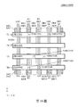
第2圖為本發明一些實施例中,積體電路布局圖200A和積體電路結構200B的示意圖。積體電路布局圖200A包含類金屬特性區DR1~DR4和DR8~DR11、閘極區GR1~GR5、金屬一區1R1、以及通孔區VDR1、VDR2、VGR1~VGR3、V0R1、及V0R2。相應地,積體電路結構200B包含類金屬特性段MD1~MD4和MD8~MD11、閘極結構G1~G5、金屬一段M11、以及通孔結構VD1、VD2、VG1~VG3、V01、及V02。
Figure 2 is a schematic diagram of an
各類金屬特性區DR1~DR4部分重疊主動區AR1,使得類金屬特性段MD1~MD4覆蓋主動區塊AA1;各類金屬特性區DR8~DR11部分重疊主動區AR2,使得類金屬特性段MD8~MD11覆蓋主動區塊AA2。金屬一區1R1與每個 金屬零區ZR1~ZR4相交於閘極區GR3和GR4之間,使得金屬一段M11於閘極結構G3和G4間部分重疊各金屬零段M01~M04。 Various metallic characteristic areas DR1~DR4 partially overlap active area AR1, making metal-like characteristic sections MD1~MD4 cover active area AA1; various metallic characteristic areas DR8~DR11 partially overlap active area AR2, making metallic-like characteristic sections MD8~MD11 Cover active block AA2. Metal one zone 1R1 with each The metal zero regions ZR1~ZR4 intersect between the gate regions GR3 and GR4, so that the metal segment M11 partially overlaps the metal zero segments M01~M04 between the gate structures G3 and G4.
通孔區VDR1部分重疊類金屬特性區DR2和金屬零區ZR1,使得通孔結構VD1將類金屬特性段MD2電性連接至金屬零段M01;通孔區VDR2部分重疊類金屬特性區DR10和金屬零區ZR4,使得通孔結構VD2將類金屬特性段MD10電性連接至金屬零段M04。通孔區VGR1部分重疊閘極區GR3和金屬零區ZR2,使得通孔結構VG1將閘極結構G3電性連接至金屬零段M02;通孔區VGR2部分重疊閘極區GR2和金屬零區ZR3,使得通孔結構VG2將閘極結構G2電性連接至金屬零段M03;通孔區VGR3部分重疊閘極區GR4和金屬零區ZR3,使得通孔結構VG3將閘極結構G4電性連接至金屬零段M03。通孔區V0R1部分重疊金屬零區ZR1和金屬一區1R1,使得通孔結構V01將通孔零段M01電性連接至金屬一段M11;通孔區V0R2部分重疊金屬零區ZR4和金屬一區1R1,使得通孔結構V02將通孔零段M04電性連接至金屬一段M11。 The via region VDR1 partially overlaps the metal-like feature region DR2 and the metal zero region ZR1, so that the via structure VD1 electrically connects the metal-like feature section MD2 to the metal zero section M01; the via region VDR2 partially overlaps the metal-like feature region DR10 and the metal The zero zone ZR4 enables the via structure VD2 to electrically connect the metal-like characteristic segment MD10 to the metal zero segment M04. The via region VGR1 partially overlaps the gate region GR3 and the metal zero region ZR2, so that the via structure VG1 electrically connects the gate structure G3 to the metal zero region M02; the via region VGR2 partially overlaps the gate region GR2 and the metal zero region ZR3 , Making the via structure VG2 electrically connect the gate structure G2 to the metal zero section M03; the via region VGR3 partially overlaps the gate region GR4 and the metal zero region ZR3, so that the via structure VG3 electrically connects the gate structure G4 to Metal zero segment M03. The via region V0R1 partially overlaps the metal zero region ZR1 and the first metal region 1R1, so that the via structure V01 electrically connects the via zero section M01 to the metal section M11; the via region V0R2 partially overlaps the metal zero region ZR4 and the first metal region 1R1 , So that the through hole structure V02 electrically connects the zero section M04 of the through hole to the metal section M11.
與電晶體P1相應之閘極區GR2與主動區AR1的相交處,包含與閘極A1等效之閘極結構G2的一部分,以及在閘極結構G2之下且與其相鄰之部分主動區塊AA1。與電晶體P2相應之閘極區GR3與主動區AR1的相交處,包含與閘極B1等效之閘極結構G3的一部分,以及在閘極結構G3之下且與其相鄰之部分主動區塊AA1。與電晶體N1相應之閘極區GR3與主動區AR2的相交處,包含與閘極B2等效之閘極結構G3的一部分,以及在閘極結構G3之下且與其相鄰之部分主動區塊AA2。 與電晶體N2相應之閘極區GR4與主動區AR2的相交處,包含與閘極A2等效之閘極結構G4的一部分,以及在閘極結構G4之下且與其相鄰之部分主動區塊AA2。 The intersection of the gate region GR2 corresponding to the transistor P1 and the active region AR1 includes a part of the gate structure G2 equivalent to the gate A1, and a part of the active block under and adjacent to the gate structure G2 AA1. The intersection of the gate region GR3 corresponding to the transistor P2 and the active region AR1 includes a part of the gate structure G3 equivalent to the gate B1, and a part of the active block under and adjacent to the gate structure G3 AA1. The intersection of the gate region GR3 corresponding to the transistor N1 and the active region AR2 includes a part of the gate structure G3 equivalent to the gate B2, and a part of the active block under and adjacent to the gate structure G3 AA2. The intersection of the gate region GR4 corresponding to the transistor N2 and the active region AR2 includes a part of the gate structure G4 equivalent to the gate A2, and a part of the active area below and adjacent to the gate structure G4 AA2.
基於積體電路布局圖200A所生之積體電路結構200B,從而包含導電路徑PA、PB、及PC。導電路徑PA介於閘極A1和A2間,且包含閘極結構G2、通孔結構VG2、金屬零段M03、通孔結構VG3、以及閘極結構G4;導電路徑PB介於閘極B1和B2間,且包含閘極結構G3;導電路徑PC包含類金屬特性段MD2(覆蓋主動區塊AA1中與電晶體P1和P2共享的部分)、通孔結構VD1、金屬零段M01、通孔結構V01、金屬一段M11、通孔結構V02、金屬零段M04、通孔結構VD2、及類金屬特性段MD10(覆蓋主動區塊AA2中與電晶體N1和N2共享的部分)。
The
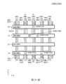
第3圖為本發明一些實施例中,積體電路布局圖300A和積體電路結構300B的示意圖。積體電路布局圖300A包含類金屬特性區DR1~DR4和DR8~DR11、閘極區GR1~GR5、金屬一區1R1、以及通孔區VDR1、VDR2、VGR1~VGR3、V0R1、及V0R2。相應地,積體電路結構300B包含類金屬特性段MD1~MD4和MD8~MD11、閘極結構G1~G5、金屬一段M11、以及通孔結構VD1、VD2、VG1~VG3、V01、及V02。
FIG. 3 is a schematic diagram of an
各類金屬特性區DR1~DR4部分重疊主動區AR1,使得類金屬特性段MD1~MD4覆蓋主動區塊AA1;各類金屬特性區DR8~DR11部分重疊主動區AR2,使得類金屬特性段MD8~MD11覆蓋主動區塊AA2。金屬一區1R1與每個 金屬零區ZR1~ZR4相交於閘極區GR3和GR4之間,使得金屬一段M11於閘極結構G3和G4間部分重疊各金屬零段M01~M04。 Various metallic characteristic areas DR1~DR4 partially overlap active area AR1, making metal-like characteristic sections MD1~MD4 cover active area AA1; various metallic characteristic areas DR8~DR11 partially overlap active area AR2, making metallic-like characteristic sections MD8~MD11 Cover active block AA2. Metal one zone 1R1 with each The metal zero regions ZR1~ZR4 intersect between the gate regions GR3 and GR4, so that the metal segment M11 partially overlaps the metal zero segments M01~M04 between the gate structures G3 and G4.
通孔區VDR1部分重疊類金屬特性區DR3和金屬零區ZR1,使得通孔結構VD1將類金屬特性段MD3電性連接至金屬零段M01;通孔區VDR2部分重疊類金屬特性區DR9和金屬零區ZR4,使得通孔結構VD2將類金屬特性段MD9電性連接至金屬零段M04。通孔區VGR1部分重疊閘極區GR2和金屬零區ZR2,使得通孔結構VG1將閘極結構G2電性連接至金屬零段M02;通孔區VGR2部分重疊閘極區GR4和金屬零區ZR2,使得通孔結構VG2將閘極結構G4電性連接至金屬零段M02;通孔區VGR3部分重疊閘極區GR3和金屬零區ZR3,使得通孔結構VG3將閘極結構G3電性連接至金屬零段M03。通孔區V0R1部分重疊金屬零區ZR1和金屬一區1R1,使得通孔結構V01將通孔零段M01電性連接至金屬一段M11;通孔區V0R2部分重疊金屬零區ZR4和金屬一區1R1,使得通孔結構V02將通孔零段M04電性連接至金屬一段M11。 The via region VDR1 partially overlaps the metal-like feature region DR3 and the metal zero region ZR1, so that the via structure VD1 electrically connects the metal-like feature section MD3 to the metal zero section M01; the via region VDR2 partially overlaps the metal-like feature region DR9 and the metal The zero zone ZR4 enables the via structure VD2 to electrically connect the metal-like characteristic segment MD9 to the metal zero segment M04. The via region VGR1 partially overlaps the gate region GR2 and the metal zero region ZR2, so that the via structure VG1 electrically connects the gate structure G2 to the metal zero region M02; the via region VGR2 partially overlaps the gate region GR4 and the metal zero region ZR2 , Making the via structure VG2 electrically connect the gate structure G4 to the metal zero segment M02; the via region VGR3 partially overlaps the gate region GR3 and the metal zero region ZR3, so that the via structure VG3 electrically connects the gate structure G3 to Metal zero segment M03. The via region V0R1 partially overlaps the metal zero region ZR1 and the first metal region 1R1, so that the via structure V01 electrically connects the via zero section M01 to the metal section M11; the via region V0R2 partially overlaps the metal zero region ZR4 and the first metal region 1R1 , So that the through hole structure V02 electrically connects the zero section M04 of the through hole to the metal section M11.
與電晶體P1相應之閘極區GR3與主動區AR1的相交處,包含與閘極A1等效之閘極結構G3的一部分,以及在閘極結構G3之下且與其相鄰之部分主動區塊AA1。與電晶體P2相應之閘極區GR4與主動區AR1的相交處,包含與閘極B1等效之閘極結構G4的一部分,以及在閘極結構G4之下且與其相鄰之部分主動區塊AA1。與電晶體N1相應之閘極區GR2與主動區AR2的相交處,包含與閘極B2等效之閘極結構G2的一部分,以及在閘極結構G2之下且與其相鄰之部分主動區塊AA2。 與電晶體N2相應之閘極區GR3與主動區AR2的相交處,包含與閘極A2等效之閘極結構G3的一部分,以及在閘極結構G3之下且與其相鄰之部分主動區塊AA2。 The intersection of the gate region GR3 corresponding to the transistor P1 and the active region AR1 includes a part of the gate structure G3 equivalent to the gate A1, and a part of the active area below and adjacent to the gate structure G3 AA1. The intersection of the gate region GR4 corresponding to the transistor P2 and the active region AR1 includes a part of the gate structure G4 equivalent to the gate B1, and a part of the active area below and adjacent to the gate structure G4 AA1. The intersection of the gate region GR2 corresponding to the transistor N1 and the active region AR2 includes a part of the gate structure G2 equivalent to the gate B2, and a part of the active block under and adjacent to the gate structure G2 AA2. The intersection of the gate region GR3 corresponding to the transistor N2 and the active region AR2 includes a part of the gate structure G3 equivalent to the gate A2, and a part of the active area below and adjacent to the gate structure G3 AA2.
基於積體電路布局圖300A所生之積體電路結構300B,從而包含導電路徑PA、PB、及PC。導電路徑PA介於閘極A1和A2間,且包含閘極結構G3;導電路徑PB介於閘極B1和B2間,且包含閘極結構G4、通孔結構VG2、金屬零段M02、通孔結構VG1、以及閘極結構G2;;導電路徑PC包含類金屬特性段MD3(覆蓋主動區塊AA1中與電晶體P1和P2共享的部分)、通孔結構VD1、金屬零段M01、通孔結構V01、金屬一段M11、通孔結構V02、金屬零段M04、通孔結構VD2、及類金屬特性段MD09(覆蓋主動區塊AA2中與電晶體N1和N2共享的部分)。
The
第4圖為本發明一些實施例中,積體電路布局圖400A和積體電路結構400B的示意圖。積體電路布局圖400A包含類金屬特性區DR1~DR5和DR8~DR12、閘極區GR1~GR6、金屬一區1R1、以及通孔區VDR1~VDR4、VGR1~VGR4、V0R1、及V0R2。相應地,積體電路結構400B包含類金屬特性段MD1~MD5和MD8~MD12、閘極結構G1~G6、金屬一段M11、以及通孔結構VD1~VDR4、VG1~VG4、V01、及V02。
FIG. 4 is a schematic diagram of an
各類金屬特性區DR1~DR5部分重疊主動區AR1,使得類金屬特性段MD1~MD5覆蓋主動區塊AA1;各類金屬特性區DR8~DR12部分重疊主動區AR2,使得類金屬特性段MD8~MD12覆蓋主動區塊AA2。金屬一區1R1與每個 金屬零區ZR1~ZR4相交於閘極區GR3和GR4之間,使得金屬一段M11部分重疊各金屬零段M01~M04於閘極結構G3和G4間。 Various metallic characteristic areas DR1~DR5 partially overlap active area AR1, making metal-like characteristic sections MD1~MD5 cover active area AA1; various metallic characteristic areas DR8~DR12 partially overlap active area AR2, making metallic-like characteristic sections MD8~MD12 Cover active block AA2. Metal one zone 1R1 with each The metal zero regions ZR1~ZR4 intersect between the gate regions GR3 and GR4, so that the metal segment M11 partially overlaps the metal zero segments M01~M04 between the gate structures G3 and G4.
通孔區VDR1部分重疊類金屬特性區DR3和金屬零區ZR1,使得通孔結構VD1將類金屬特性段MD3電性連接至金屬零段M01;通孔區VDR2部分重疊類金屬特性區DR4和金屬零區ZR1,使得通孔結構VD2將類金屬特性段MD4電性連接至金屬零段M01;通孔區VDR3部分重疊類金屬特性區DR9和金屬零區ZR4,使得通孔結構VD3將類金屬特性段MD9電性連接至金屬零段M04;通孔區VGR4部分重疊類金屬特性區DR10和金屬零區ZR4,使得通孔結構VD4將類金屬特性段MD10電性連接至金屬零段M04。通孔區VGR1部分重疊閘極區GR3和金屬零區ZR2,使得通孔結構VG1將閘極結構G3電性連接至金屬零段M02;通孔區VGR2部分重疊閘極區GR4和金屬零區ZR2,使得通孔結構VG2將閘極結構G4電性連接至金屬零段M02;通孔區VGR3部分重疊閘極區GR2和金屬零區ZR3,使得通孔結構VG3將閘極結構G2電性連接至金屬零段M03;通孔區VGR4部分重疊閘極區GR5和金屬零區ZR3,使得通孔結構VG4將閘極結構G5電性連接至金屬零段M03。通孔區V0R1部分重疊金屬零區ZR1和金屬一區1R1,使得通孔結構V01將通孔零段M01電性連接至金屬一段M11;通孔區V0R2部分重疊金屬零區ZR4和金屬一區1R1,使得通孔結構V02將通孔零段M04電性連接至金屬一段M11。 The via region VDR1 partially overlaps the metal-like feature region DR3 and the metal zero region ZR1, so that the via structure VD1 electrically connects the metal-like feature section MD3 to the metal zero section M01; the via region VDR2 partially overlaps the metal-like feature region DR4 and the metal Zero zone ZR1 makes the through-hole structure VD2 electrically connect the metal-like characteristic section MD4 to the metal zero section M01; the through-hole area VDR3 partially overlaps the metal-like characteristic zone DR9 and the metal zero zone ZR4, so that the through-hole structure VD3 has a metal-like characteristic The segment MD9 is electrically connected to the metal zero segment M04; the via region VGR4 partially overlaps the metal-like feature region DR10 and the metal zero region ZR4, so that the via structure VD4 electrically connects the metal-like feature segment MD10 to the metal zero segment M04. The via region VGR1 partially overlaps the gate region GR3 and the metal zero region ZR2, so that the via structure VG1 electrically connects the gate structure G3 to the metal zero region M02; the via region VGR2 partially overlaps the gate region GR4 and the metal zero region ZR2 , Making the via structure VG2 electrically connect the gate structure G4 to the metal zero segment M02; the via region VGR3 partially overlaps the gate region GR2 and the metal zero region ZR3, so that the via structure VG3 electrically connects the gate structure G2 to Metal zero segment M03; the via region VGR4 partially overlaps the gate region GR5 and the metal zero region ZR3, so that the via structure VG4 electrically connects the gate structure G5 to the metal zero segment M03. The via region V0R1 partially overlaps the metal zero region ZR1 and the first metal region 1R1, so that the via structure V01 electrically connects the via zero section M01 to the metal section M11; the via region V0R2 partially overlaps the metal zero region ZR4 and the first metal region 1R1 , So that the through hole structure V02 electrically connects the zero section M04 of the through hole to the metal section M11.
與電晶體P1相應之閘極區GR3與主動區AR1的相交處,包含與閘極A1等效之閘極結構G3的一部分,以及在 閘極結構G3之下且與其相鄰之部分主動區塊AA1。與電晶體P2相應之閘極區GR5與主動區AR1的相交處,包含與閘極B1等效之閘極結構G5的一部分,以及在閘極結構G5之下且與其相鄰之部分主動區塊AA1。與電晶體N1相應之閘極區GR2與主動區AR2的相交處,包含與閘極B2等效之閘極結構G2的一部分,以及在閘極結構G2之下且與其相鄰之部分主動區塊AA2。與電晶體N2相應之閘極區GR4與主動區AR2的相交處,包含與閘極A2等效之閘極結構G4的一部分,以及在閘極結構G4之下且與其相鄰之部分主動區塊AA2。 The intersection of the gate region GR3 corresponding to the transistor P1 and the active region AR1 includes a part of the gate structure G3 equivalent to the gate A1, and Part of the active block AA1 under and adjacent to the gate structure G3. The intersection of the gate region GR5 corresponding to the transistor P2 and the active region AR1 includes a part of the gate structure G5 equivalent to the gate B1, and a part of the active area below and adjacent to the gate structure G5 AA1. The intersection of the gate region GR2 corresponding to the transistor N1 and the active region AR2 includes a part of the gate structure G2 equivalent to the gate B2, and a part of the active block under and adjacent to the gate structure G2 AA2. The intersection of the gate region GR4 corresponding to the transistor N2 and the active region AR2 includes a part of the gate structure G4 equivalent to the gate A2, and a part of the active area below and adjacent to the gate structure G4 AA2.
基於積體電路布局圖400A所生之積體電路結構400B,從而包含導電路徑PA、PB、及PC。導電路徑PA介於閘極A1和A2間,且包含閘極結構G3、通孔結構VG1、金屬零段M02、通孔結構VG2、以及閘極結構G4;導電路徑PB介於閘極B1和B2間,且包含閘極結構G5、通孔結構VG4、金屬零段M03、通孔結構VG3、及閘極結構G2;導電路徑PC包含類金屬特性段MD3(覆蓋電晶體P1中的部分主動區塊AA1)、通孔結構VD1、類金屬特性段MD4(覆蓋電晶體P2中的部分主動區塊AA1)、通孔結構VD2、金屬零段M01、通孔結構V01、金屬一段M11、通孔結構V02、金屬零段M04、通孔結構VD3、類金屬特性段MD9(覆蓋電晶體N1中的部分主動區塊AA2)、通孔結構VD4、及類金屬特性段MD10(覆蓋電晶體N2中的部分主動區塊AA2)。
The
第5圖為本發明一些實施例中,積體電路布局圖500A和積體電路結構500B的示意圖。積體電路布局圖500A包含類金屬特性區DR1~DR5和DR8~DR12、閘極區GR1~
GR6、金屬一區1R1、以及通孔區VDR1~VDR4、VGR1~VGR4、V0R1、及V0R2。相應地,積體電路結構500B包含類金屬特性段MD1~MD5和MD8~MD12、閘極結構G1~G6、金屬一段M11、以及通孔結構VD1~VDR4、VG1~VG4、V01、及V02。
FIG. 5 is a schematic diagram of an
各類金屬特性區DR1~DR5部分重疊主動區AR1,使得類金屬特性段MD1~MD5覆蓋主動區塊AA1;各類金屬特性區DR8~DR12部分重疊主動區AR2,使得類金屬特性段MD8~MD12覆蓋主動區塊AA2。金屬一區1R1與每個金屬零區ZR1~ZR4相交於閘極區GR3和GR4之間,使得金屬一段M11於閘極結構G3和G4間部分重疊各金屬零段M01~M04。 Various metallic characteristic areas DR1~DR5 partially overlap active area AR1, making metal-like characteristic sections MD1~MD5 cover active area AA1; various metallic characteristic areas DR8~DR12 partially overlap active area AR2, making metallic-like characteristic sections MD8~MD12 Cover active block AA2. The first metal zone 1R1 and each metal zero zone ZR1~ZR4 intersect between the gate regions GR3 and GR4, so that the metal segment M11 partially overlaps the metal zero segments M01~M04 between the gate structures G3 and G4.
通孔區VDR1部分重疊類金屬特性區DR2和金屬零區ZR1,使得通孔結構VD1將類金屬特性段MD2電性連接至金屬零段M01;通孔區VDR2部分重疊類金屬特性區DR3和金屬零區ZR1,使得通孔結構VD2將類金屬特性段MD3電性連接至金屬零段M01;通孔區VDR3部分重疊類金屬特性區DR10和金屬零區ZR4,使得通孔結構VD3將類金屬特性段MD10電性連接至金屬零段M04;通孔區VDR4部分重疊類金屬特性區DR11和金屬零區ZR4,使得通孔結構VD4將類金屬特性段MD11電性連接至金屬零段M04。通孔區VGR1部分重疊閘極區GR2和金屬零區ZR2,使得通孔結構VG1將閘極結構G2電性連接至金屬零段M02;通孔區VGR2部分重疊閘極區GR5和金屬零區ZR2,使得通孔結構VG2將閘極結構G5電性連接至金屬零段M02;通孔區VGR3部分重疊閘極區GR3和金屬零區 ZR3,使得通孔結構VG3將閘極結構G3電性連接至金屬零段M03;通孔區VGR4部分重疊閘極區GR4和金屬零區ZR3,使得通孔結構VG4將閘極結構G4電性連接至金屬零段M03。通孔區V0R1部分重疊金屬零區ZR1和金屬一區1R1,使得通孔結構V01將通孔零段M01電性連接至金屬一段M11;通孔區V0R2部分重疊金屬零區ZR4和金屬一區1R1,使得通孔結構V02將通孔零段M04電性連接至金屬一段M11。 The via region VDR1 partially overlaps the metal-like feature region DR2 and the metal zero region ZR1, so that the via structure VD1 electrically connects the metal-like feature section MD2 to the metal zero section M01; the via region VDR2 partially overlaps the metal-like feature region DR3 and the metal Zero zone ZR1 makes the through-hole structure VD2 electrically connect the metal-like characteristic section MD3 to the metal zero section M01; the through-hole area VDR3 partially overlaps the metal-like characteristic zone DR10 and the metal zero zone ZR4, so that the through-hole structure VD3 has a metal-like characteristic The segment MD10 is electrically connected to the metal zero segment M04; the via region VDR4 partially overlaps the metal-like feature region DR11 and the metal zero region ZR4, so that the via structure VD4 electrically connects the metal-like feature segment MD11 to the metal zero segment M04. The via region VGR1 partially overlaps the gate region GR2 and the metal zero region ZR2, so that the via structure VG1 electrically connects the gate structure G2 to the metal zero region M02; the via region VGR2 partially overlaps the gate region GR5 and the metal zero region ZR2 , Making the via structure VG2 electrically connect the gate structure G5 to the metal zero section M02; the via region VGR3 partially overlaps the gate region GR3 and the metal zero region ZR3 makes the via structure VG3 electrically connect the gate structure G3 to the metal zero segment M03; the via region VGR4 partially overlaps the gate region GR4 and the metal zero region ZR3, so that the via structure VG4 electrically connects the gate structure G4 To the metal zero section M03. The via region V0R1 partially overlaps the metal zero region ZR1 and the first metal region 1R1, so that the via structure V01 electrically connects the via zero section M01 to the metal section M11; the via region V0R2 partially overlaps the metal zero region ZR4 and the first metal region 1R1 , So that the through hole structure V02 electrically connects the zero section M04 of the through hole to the metal section M11.
與電晶體P1相應之閘極區GR2與主動區AR1的相交處,包含與閘極A1等效之閘極結構G2的一部分,以及在閘極結構G2之下且與其相鄰之部分主動區塊AA1。與電晶體P2相應之閘極區GR4與主動區AR1的相交處,包含與閘極B1等效之閘極結構G4的一部分,以及在閘極結構G4之下且與其相鄰之部分主動區塊AA1。與電晶體N1相應之閘極區GR3與主動區AR2的相交處,包含與閘極B2等效之閘極結構G3的一部分,以及在閘極結構G3之下且與其相鄰之部分主動區塊AA2。與電晶體N2相應之閘極區GR5與主動區AR2的相交處,包含與閘極A2等效之閘極結構G5的一部分,以及在閘極結構G5之下且與其相鄰之部分主動區塊AA2。 The intersection of the gate region GR2 corresponding to the transistor P1 and the active region AR1 includes a part of the gate structure G2 equivalent to the gate A1, and a part of the active block under and adjacent to the gate structure G2 AA1. The intersection of the gate region GR4 corresponding to the transistor P2 and the active region AR1 includes a part of the gate structure G4 equivalent to the gate B1, and a part of the active area below and adjacent to the gate structure G4 AA1. The intersection of the gate region GR3 corresponding to the transistor N1 and the active region AR2 includes a part of the gate structure G3 equivalent to the gate B2, and a part of the active block under and adjacent to the gate structure G3 AA2. The intersection of the gate region GR5 corresponding to the transistor N2 and the active region AR2 includes a part of the gate structure G5 equivalent to the gate A2, and a part of the active block under and adjacent to the gate structure G5 AA2.
基於積體電路布局圖500A所生之積體電路結構500B,從而包含導電路徑PA、PB、及PC。導電路徑PA介於閘極A1和A2間,且包含閘極結構G2、通孔結構VG1、金屬零段M02、通孔結構VG2、以及閘極結構G5;導電路徑PB介於閘極B1和B2間,且包含閘極結構G4、通孔結構VG4、金屬零段M03、通孔結構VG3、及閘極結構G3;導電路徑PC包含類金屬特性段MD2(覆蓋電晶體P1中的部分主動區塊AA1)、
通孔結構VD1、類金屬特性段MD3(覆蓋電晶體P2中的部分主動區塊AA1)、通孔結構VD2、金屬零段M01、通孔結構V01、金屬一段M11、通孔結構V02、金屬零段M04、通孔結構VD3、類金屬特性段MD10(覆蓋電晶體N1中的部分主動區塊AA2)、通孔結構VD4、及類金屬特性段MD11(覆蓋電晶體N2中的部分主動區塊AA2)。
The
第6圖為本發明一些實施例中,積體電路布局圖600A和積體電路結構600B的示意圖。積體電路布局圖600A包含類金屬特性區DR1~DR5和DR8~DR12、閘極區GR1~GR6、金屬一區1R1、以及通孔區VDR1~VDR4、VGR1~VGR4、V0R1、及V0R2。相應地,積體電路結構600B包含類金屬特性段MD1~MD5和MD8~MD12、閘極結構G1~G6、金屬一段M11、以及通孔結構VD1~VDR4、VG1~VG4、V01、及V02。
FIG. 6 is a schematic diagram of an
各類金屬特性區DR1~DR5部分重疊主動區AR1,使得類金屬特性段MD1~MD5覆蓋主動區塊AA1;各類金屬特性區DR8~DR12部分重疊主動區AR2,使得類金屬特性段MD8~MD12覆蓋主動區塊AA2。金屬一區1R1與每個金屬零區ZR1~ZR4相交於閘極區GR3和GR4之間,使得金屬一段M11部分重疊各金屬零段M01~M04於閘極結構G3和G4間。 Various metallic characteristic areas DR1~DR5 partially overlap active area AR1, making metal-like characteristic sections MD1~MD5 cover active area AA1; various metallic characteristic areas DR8~DR12 partially overlap active area AR2, making metallic-like characteristic sections MD8~MD12 Cover active block AA2. The first metal region 1R1 and each metal zero region ZR1~ZR4 intersect between the gate regions GR3 and GR4, so that the metal section M11 partially overlaps the metal zero sections M01~M04 between the gate structures G3 and G4.
通孔區VDR1部分重疊類金屬特性區DR2和金屬零區ZR1,使得通孔結構VD1將類金屬特性段MD2電性連接至金屬零段M01;通孔區VDR2部分重疊類金屬特性區DR3和金屬零區ZR1,使得通孔結構VD2將類金屬特性段MD3電性連接 至金屬零段M01;通孔區VDR3部分重疊類金屬特性區DR4和金屬零區ZR1,使得通孔結構VD3將類金屬特性段MD4電性連接至金屬零段M01;通孔區VDR4部分重疊類金屬特性區DR10和金屬零區ZR4,使得通孔結構VD4將類金屬特性段MD10電性連接至金屬零段M04。通孔區VGR1部分重疊閘極區GR2和金屬零區ZR2,使得通孔結構VG1將閘極結構G2電性連接至金屬零段M02;通孔區VGR2部分重疊閘極區GR4和金屬零區ZR2,使得通孔結構VG2將閘極結構G4電性連接至金屬零段M02;通孔區VGR3部分重疊閘極區GR3和金屬零區ZR3,使得通孔結構VG3將閘極結構G3電性連接至金屬零段M03;通孔區VGR4部分重疊閘極區GR5和金屬零區ZR3,使得通孔結構VG4將閘極結構G5電性連接至金屬零段M03。通孔區V0R1部分重疊金屬零區ZR1和金屬一區1R1,使得通孔結構V01將通孔零段M01電性連接至金屬一段M11;通孔區V0R2部分重疊金屬零區ZR4和金屬一區1R1,使得通孔結構V02將通孔零段M04電性連接至金屬一段M11。 The via region VDR1 partially overlaps the metal-like feature region DR2 and the metal zero region ZR1, so that the via structure VD1 electrically connects the metal-like feature section MD2 to the metal zero section M01; the via region VDR2 partially overlaps the metal-like feature region DR3 and the metal Zero zone ZR1 makes the through-hole structure VD2 electrically connect the metal-like characteristic segment MD3 To the metal zero segment M01; the via region VDR3 partially overlaps the metal-like feature region DR4 and the metal zero region ZR1, so that the via structure VD3 electrically connects the metal-like feature segment MD4 to the metal zero segment M01; the via region VDR4 partially overlaps The metal characteristic zone DR10 and the metal zero zone ZR4 enable the via structure VD4 to electrically connect the metal-like characteristic section MD10 to the metal zero section M04. The via region VGR1 partially overlaps the gate region GR2 and the metal zero region ZR2, so that the via structure VG1 electrically connects the gate structure G2 to the metal zero region M02; the via region VGR2 partially overlaps the gate region GR4 and the metal zero region ZR2 , Making the via structure VG2 electrically connect the gate structure G4 to the metal zero segment M02; the via region VGR3 partially overlaps the gate region GR3 and the metal zero region ZR3, so that the via structure VG3 electrically connects the gate structure G3 to Metal zero segment M03; the via region VGR4 partially overlaps the gate region GR5 and the metal zero region ZR3, so that the via structure VG4 electrically connects the gate structure G5 to the metal zero segment M03. The via region V0R1 partially overlaps the metal zero region ZR1 and the first metal region 1R1, so that the via structure V01 electrically connects the via zero section M01 to the metal section M11; the via region V0R2 partially overlaps the metal zero region ZR4 and the first metal region 1R1 , So that the through hole structure V02 electrically connects the zero section M04 of the through hole to the metal section M11.
與電晶體P1相應之閘極區GR2與主動區AR1的相交處,包含與閘極A1等效之閘極結構G2的一部分,以及在閘極結構G2之下且與其相鄰之部分主動區塊AA1。與電晶體P2相應之閘極區GR5與主動區AR1的相交處,包含與閘極B1等效之閘極結構G5的一部分,以及在閘極結構G5之下且與其相鄰之部分主動區塊AA1。與電晶體N1相應之閘極區GR3與主動區AR2的相交處,包含與閘極B2等效之閘極結構G3的一部分,以及在閘極結構G3之下且與其相鄰之部分主動區塊AA2。與電晶體N2相應之閘極區GR4與主動區AR2的相交處,包含與 閘極A2等效之閘極結構G4的一部分,以及在閘極結構G4之下且與其相鄰之部分主動區塊AA2。 The intersection of the gate region GR2 corresponding to the transistor P1 and the active region AR1 includes a part of the gate structure G2 equivalent to the gate A1, and a part of the active block under and adjacent to the gate structure G2 AA1. The intersection of the gate region GR5 corresponding to the transistor P2 and the active region AR1 includes a part of the gate structure G5 equivalent to the gate B1, and a part of the active area below and adjacent to the gate structure G5 AA1. The intersection of the gate region GR3 corresponding to the transistor N1 and the active region AR2 includes a part of the gate structure G3 equivalent to the gate B2, and a part of the active block under and adjacent to the gate structure G3 AA2. The intersection of the gate region GR4 corresponding to the transistor N2 and the active region AR2 includes A part of the gate structure G4 equivalent to the gate A2, and a part of the active block AA2 under and adjacent to the gate structure G4.
基於積體電路布局圖600A所生之積體電路結構600B,從而包含導電路徑PA、PB、及PC。導電路徑PA介於閘極A1和A2間,且包含閘極結構G2、通孔結構VG1、金屬零段M02、通孔結構VG2、以及閘極結構G4;導電路徑PB介於閘極B1和B2間,且包含閘極結構G5、通孔結構VG4、金屬零段M03、通孔結構VG3、及閘極結構G3;導電路徑PC包含類金屬特性段MD2(覆蓋電晶體P1中的部分主動區塊AA1)、通孔結構VD1、類金屬特性段MD3(覆蓋其他未受控制的部分主動區塊AA1)、通孔結構VD2、類金屬特性段MD4(覆蓋電晶體P2中的部分主動區塊AA1)、金屬零段M01、通孔結構V01、金屬一段M11、通孔結構V02、金屬零段M04、通孔結構VD3、及類金屬特性段MD10(覆蓋電晶體N1和N2共享之部分主動區塊AA2)。
The
第7圖為本發明一些實施例中,積體電路布局圖700A和積體電路結構700B的示意圖。積體電路布局圖700A包含類金屬特性區DR1~DR5和DR8~DR12、閘極區GR1~GR6、金屬一區1R1、以及通孔區VDR1~VDR4、VGR1~VGR4、V0R1、及V0R2。相應地,積體電路結構700B包含類金屬特性段MD1~MD5和MD8~MD12、閘極結構G1~G6、金屬一段M11、以及通孔結構VD1~VDR4、VG1~VG4、V01、及V02。
FIG. 7 is a schematic diagram of an
各類金屬特性區DR1~DR5部分重疊主動區AR1,使得類金屬特性段MD1~MD5覆蓋主動區塊AA1;各 類金屬特性區DR8~DR12部分重疊主動區AR2,使得類金屬特性段MD8~MD12覆蓋主動區塊AA2。金屬一區1R1與每個金屬零區ZR1~ZR4相交於閘極區GR3和GR4之間,使得金屬一段M11部分重疊各金屬零段M01~M04於閘極結構G3和G4間。 The various metallic characteristic areas DR1~DR5 partially overlap the active area AR1, so that the metal-like characteristic sections MD1~MD5 cover the active area AA1; The metal-like characteristic areas DR8 to DR12 partially overlap the active area AR2, so that the metal-like characteristic areas MD8 to MD12 cover the active area AA2. The first metal region 1R1 and each metal zero region ZR1~ZR4 intersect between the gate regions GR3 and GR4, so that the metal section M11 partially overlaps the metal zero sections M01~M04 between the gate structures G3 and G4.
通孔區VDR1部分重疊類金屬特性區DR3和金屬零區ZR1,使得通孔結構VD1將類金屬特性段MD3電性連接至金屬零段M01;通孔區VDR2部分重疊類金屬特性區DR9和金屬零區ZR4,使得通孔結構VD2將類金屬特性段MD9電性連接至金屬零段M04;通孔區VDR3部分重疊類金屬特性區DR10和金屬零區ZR4,使得通孔結構VD3將類金屬特性段MD10電性連接至金屬零段M04;通孔區VDR4部分重疊類金屬特性區DR11和金屬零區ZR4,使得通孔結構VD4將類金屬特性段MD11電性連接至金屬零段M04。通孔區VGR1部分重疊閘極區GR3和金屬零區ZR2,使得通孔結構VG1將閘極結構G3電性連接至金屬零段M02;通孔區VGR2部分重疊閘極區GR5和金屬零區ZR2,使得通孔結構VG2將閘極結構G5電性連接至金屬零段M02;通孔區VGR3部分重疊閘極區GR2和金屬零區ZR3,使得通孔結構VG3將閘極結構G2電性連接至金屬零段M03;通孔區VGR4部分重疊閘極區GR4和金屬零區ZR3,使得通孔結構VG4將閘極結構G4電性連接至金屬零段M03。通孔區V0R1部分重疊金屬零區ZR1和金屬一區1R1,使得通孔結構V01將通孔零段M01電性連接至金屬一段M11;通孔區V0R2部分重疊金屬零區ZR4和金屬一區1R1,使得通孔結構V02將通孔零段M04電性連接至金屬一段M11。 The via region VDR1 partially overlaps the metal-like feature region DR3 and the metal zero region ZR1, so that the via structure VD1 electrically connects the metal-like feature section MD3 to the metal zero section M01; the via region VDR2 partially overlaps the metal-like feature region DR9 and the metal Zero zone ZR4 makes the through-hole structure VD2 electrically connect the metal-like characteristic section MD9 to the metal zero section M04; the through-hole area VDR3 partially overlaps the metal-like characteristic zone DR10 and the metal zero zone ZR4, so that the through-hole structure VD3 has a metal-like characteristic The segment MD10 is electrically connected to the metal zero segment M04; the via region VDR4 partially overlaps the metal-like feature region DR11 and the metal zero region ZR4, so that the via structure VD4 electrically connects the metal-like feature segment MD11 to the metal zero segment M04. The via region VGR1 partially overlaps the gate region GR3 and the metal zero region ZR2, so that the via structure VG1 electrically connects the gate structure G3 to the metal zero region M02; the via region VGR2 partially overlaps the gate region GR5 and the metal zero region ZR2 , Making the via structure VG2 electrically connect the gate structure G5 to the metal zero segment M02; the via region VGR3 partially overlaps the gate region GR2 and the metal zero region ZR3, so that the via structure VG3 electrically connects the gate structure G2 to Metal zero segment M03; the via region VGR4 partially overlaps the gate region GR4 and the metal zero region ZR3, so that the via structure VG4 electrically connects the gate structure G4 to the metal zero segment M03. The via region V0R1 partially overlaps the metal zero region ZR1 and the first metal region 1R1, so that the via structure V01 electrically connects the via zero section M01 to the metal section M11; the via region V0R2 partially overlaps the metal zero region ZR4 and the first metal region 1R1 , So that the through hole structure V02 electrically connects the zero section M04 of the through hole to the metal section M11.
與電晶體P1相應之閘極區GR3與主動區AR1的相交處,包含與閘極A1等效之閘極結構G3的一部分,以及在閘極結構G3之下且與其相鄰之部分主動區塊AA1。與電晶體P2相應之閘極區GR4與主動區AR1的相交處,包含與閘極B1等效之閘極結構G4的一部分,以及在閘極結構G4之下且與其相鄰之部分主動區塊AA1。與電晶體N1相應之閘極區GR2與主動區AR2的相交處,包含與閘極B2等效之閘極結構G2的一部分,以及在閘極結構G2之下且與其相鄰之部分主動區塊AA2。與電晶體N2相應之閘極區GR5與主動區AR2的相交處,包含與閘極A2等效之閘極結構G5的一部分,以及在閘極結構G5之下且與其相鄰之部分主動區塊AA2。 The intersection of the gate region GR3 corresponding to the transistor P1 and the active region AR1 includes a part of the gate structure G3 equivalent to the gate A1, and a part of the active area below and adjacent to the gate structure G3 AA1. The intersection of the gate region GR4 corresponding to the transistor P2 and the active region AR1 includes a part of the gate structure G4 equivalent to the gate B1, and a part of the active area below and adjacent to the gate structure G4 AA1. The intersection of the gate region GR2 corresponding to the transistor N1 and the active region AR2 includes a part of the gate structure G2 equivalent to the gate B2, and a part of the active block under and adjacent to the gate structure G2 AA2. The intersection of the gate region GR5 corresponding to the transistor N2 and the active region AR2 includes a part of the gate structure G5 equivalent to the gate A2, and a part of the active block under and adjacent to the gate structure G5 AA2.
基於積體電路布局圖700A所生之積體電路結構700B,從而包含導電路徑PA、PB、及PC。導電路徑PA介於閘極A1和A2間,且包含閘極結構G3、通孔結構VG1、金屬零段M02、通孔結構VG2、以及閘極結構G5;導電路徑PB介於閘極B1和B2間,且包含閘極結構G4、通孔結構VG4、金屬零段M03、通孔結構VG3、及閘極結構G2;導電路徑PC包含類金屬特性段MD3(覆蓋電晶體P1和P2共享之部分主動區塊AA1)、通孔結構VD1、金屬零段M01、通孔結構V01、金屬一段M11、通孔結構V02、金屬零段M04、通孔結構VD2、類金屬特性段MD9(覆蓋電晶體N1中的部分主動區塊AA2)、通孔結構VD3、類金屬特性段MD10(覆蓋其他未受控制的部分主動區塊AA2)、通孔結構VD4、及類金屬特性段MD11(覆蓋電晶體N2中的部分主動區塊AA2)。
The
第8圖為本發明一些實施例中,積體電路布局圖
800A和積體電路結構800B的示意圖。積體電路布局圖800A包含類金屬特性區DR1~DR3、DR8、DR10、閘極區GR1~GR4、及通孔區VGR1及VGR2。相應地,積體電路結構800B包含類金屬特性段MD1~MD3、MD8、MD10、閘極區G1~G4、及通孔區VG1及VG2。
Figure 8 is a layout diagram of an integrated circuit in some embodiments of the present invention
Schematic diagram of 800A and
各類金屬特性區DR1和DR3部分重疊主動區AR1,使得類金屬特性段MD1和MD3覆蓋主動區塊AA1;類金屬特性區DR2部分重疊主動區AR1和AR2,使得類金屬特性段MD2覆蓋主動區塊AA1和AA2;各類金屬特性區DR8和DR10部分重疊主動區AR2,使得類金屬特性段MD8和MD10覆蓋主動區塊AA2。通孔區VGR1部分重疊閘極區GR2及金屬零區ZR1,使得通孔結構VG1將閘極結構G2電性連接至金屬零段M01;通孔區VGR2部分重疊閘極區GR3及金屬零區ZR4,使得通孔結構VG2將閘極結構G3電性連接至金屬零段M04。 Various metallic characteristic areas DR1 and DR3 partially overlap the active area AR1, so that the metal-like characteristic sections MD1 and MD3 cover the active area AA1; the metallic-like characteristic area DR2 partially overlaps the active areas AR1 and AR2, so that the metallic-like characteristic section MD2 covers the active area Blocks AA1 and AA2; the various metal characteristic areas DR8 and DR10 partially overlap the active area AR2, so that the metal-like characteristic sections MD8 and MD10 cover the active area AA2. The via region VGR1 partially overlaps the gate region GR2 and the metal zero region ZR1, so that the via structure VG1 electrically connects the gate structure G2 to the metal zero region M01; the via region VGR2 partially overlaps the gate region GR3 and the metal zero region ZR4 , So that the via structure VG2 electrically connects the gate structure G3 to the metal zero segment M04.
與電晶體P1相應之閘極區GR2與主動區AR1的相交處,包含與閘極A1等效之閘極結構G2的一部分,以及在閘極結構G2之下且與其相鄰之部分主動區塊AA1。與電晶體P2相應之閘極區GR3與主動區AR1的相交處,包含與閘極B1等效之閘極結構G3的一部分,以及在閘極結構G3之下且與其相鄰之部分主動區塊AA1。與電晶體N1相應之閘極區GR3與主動區AR2的相交處,包含與閘極B2等效之閘極結構G3的一部分,以及在閘極結構G3之下且與其相鄰之部分主動區塊AA2。與電晶體N2相應之閘極區GR2與主動區AR2的相交處,包含與閘極A2等效之閘極結構G2的一部分,以及在閘極結構G2之下且與其相鄰之部分主動區塊AA2。 The intersection of the gate region GR2 corresponding to the transistor P1 and the active region AR1 includes a part of the gate structure G2 equivalent to the gate A1, and a part of the active block under and adjacent to the gate structure G2 AA1. The intersection of the gate region GR3 corresponding to the transistor P2 and the active region AR1 includes a part of the gate structure G3 equivalent to the gate B1, and a part of the active block under and adjacent to the gate structure G3 AA1. The intersection of the gate region GR3 corresponding to the transistor N1 and the active region AR2 includes a part of the gate structure G3 equivalent to the gate B2, and a part of the active block under and adjacent to the gate structure G3 AA2. The intersection of the gate region GR2 corresponding to the transistor N2 and the active region AR2 includes a part of the gate structure G2 equivalent to the gate A2, and a part of the active block under and adjacent to the gate structure G2 AA2.
於積體電路布局圖800A所生之積體電路結構800B,從而包含導電路徑PA、PB、及PC。導電路徑PA介於閘極A1和A2間,且包含閘極結構G2;導電路徑PB介於閘極B1和B2間,且包含閘極結構G3;導電路徑PC包含類金屬特性段MD2(覆蓋電晶體P1和P2共享之部分主動區塊AA1以及電晶體N1和N2共享之部分主動區塊AA2)。
The
第9圖為本發明一些實施例中,積體電路布局圖900A和積體電路結構900B的示意圖。積體電路布局圖900A包含類金屬特性區DR1~DR5、DR9、DR11、閘極區GR1~GR6、及通孔區VDR1~VDR4和VGR1~VGR8。相應地,積體電路結構900B包含類金屬特性段MD1~MD5、MD9、MD11、閘極區GR1~GR6、及通孔結構VD1~VDR4和VG1~VG8。
FIG. 9 is a schematic diagram of an
各類金屬特性區DR1、DR3、及DR5部分重疊主動區AR1和AR2,使得類金屬特性段MD1、MD3、及MD5覆蓋主動區塊AA1和AA2;各類金屬特性區DR2和DR4部分重疊主動區AR1,使得類金屬特性段MD2和MD4覆蓋主動區塊AA1;各類金屬特性區DR9和DR11部分重疊主動區AR2,使得類金屬特性段MD9和MD11覆蓋主動區塊AA2。各閘極區GR3和GR4包含一間隙介於金屬零區ZR2和ZR3之間,此間隙在一些實施例中又可稱之為一切割多晶矽區,並使得各閘極結構G3和G4在金屬零段M02和M03間不導電且不連續。各金屬零區ZR1和ZR4包含一間隙介於金屬零區GR3和GR4之間,此間隙在一些實施例中又可稱之為一切割金屬零區,並使得各金屬零段M01和M04從閘極結構G3和G4間分離為不導電且不連 續性的數段。 Various metal characteristic areas DR1, DR3, and DR5 partially overlap active areas AR1 and AR2, so that metal-like characteristic sections MD1, MD3, and MD5 cover active blocks AA1 and AA2; various metal characteristic areas DR2 and DR4 partially overlap active areas AR1 makes the metal-like characteristic sections MD2 and MD4 cover the active area AA1; various metallic characteristic areas DR9 and DR11 partially overlap the active area AR2, so that the metal-like characteristic sections MD9 and MD11 cover the active area AA2. Each gate region GR3 and GR4 includes a gap between the metal zero regions ZR2 and ZR3. This gap can also be called a cut polysilicon region in some embodiments, and makes the gate structures G3 and G4 in the metal zero region. The sections M02 and M03 are non-conductive and discontinuous. Each metal zero zone ZR1 and ZR4 includes a gap between the metal zero zones GR3 and GR4. This gap can also be called a cutting metal zero zone in some embodiments, and makes each metal zero segment M01 and M04 from the gate The pole structure G3 and G4 are separated as non-conductive and not connected Several consecutive paragraphs.
通孔區VDR1部分重疊類金屬特性區DR1和金屬零區ZR1,使得通孔結構VD1將類金屬特性段MD1電性連接至金屬零段M01;通孔區VDR2部分重疊類金屬特性區DR1和金屬零區ZR3,使得通孔結構VD2將類金屬特性段MD1電性連接至金屬零段M03;通孔區VDR3部分重疊類金屬特性區DR5和金屬零區ZR3,使得通孔結構VD3將類金屬特性段MD5電性連接至金屬零段M03;通孔區VDR4部分重疊類金屬特性區DR5和金屬零區ZR4,使得通孔結構VD4將類金屬特性段MD5電性連接至金屬零段M04。通孔區VGR1部分重疊閘極區GR3和金屬零區ZR1,使得通孔結構VG1將閘極結構G3電性連接至金屬零段M01;通孔區VGR2部分重疊閘極區GR4和金屬零區ZR1,使得通孔結構VG2將閘極結構G4電性連接至金屬零段M01;通孔區VGR3部分重疊閘極區GR5和金屬零區ZR1,使得通孔結構VG3將閘極結構G5電性連接至金屬零段M01;通孔區VGR4部分重疊閘極區GR2和金屬零區ZR2,使得通孔結構VG4將閘極結構G2電性連接至金屬零段M02;通孔區VGR5部分重疊閘極區GR5和金屬零區ZR2,使得通孔結構VG5將閘極結構G5電性連接至金屬零段M02;通孔區VGR6部分重疊閘極區GR2和金屬零區ZR4,使得通孔結構VG6將閘極結構G2電性連接至金屬零段M04;通孔區VGR7部分重疊閘極區GR3和金屬零區ZR4,使得通孔結構VG7將閘極結構G3電性連接至金屬零段M04;通孔區VGR8部分重疊閘極區GR4和金屬零區ZR4,使得通孔結構VG8將閘極結構G4電性連接至金屬零段M04。 The via region VDR1 partially overlaps the metal-like feature region DR1 and the metal zero region ZR1, so that the via structure VD1 electrically connects the metal-like feature section MD1 to the metal zero section M01; the via region VDR2 partially overlaps the metal-like feature region DR1 and the metal The zero zone ZR3 makes the through-hole structure VD2 electrically connect the metal-like characteristic section MD1 to the metal zero section M03; the through-hole area VDR3 partially overlaps the metal-like characteristic zone DR5 and the metal zero zone ZR3, so that the through-hole structure VD3 has a metal-like characteristic The segment MD5 is electrically connected to the metal zero segment M03; the via region VDR4 partially overlaps the metal-like feature region DR5 and the metal zero region ZR4, so that the via structure VD4 electrically connects the metal-like feature segment MD5 to the metal zero segment M04. The via region VGR1 partially overlaps the gate region GR3 and the metal zero region ZR1, so that the via structure VG1 electrically connects the gate structure G3 to the metal zero region M01; the via region VGR2 partially overlaps the gate region GR4 and the metal zero region ZR1 , So that the via structure VG2 electrically connects the gate structure G4 to the metal zero segment M01; the via region VGR3 partially overlaps the gate region GR5 and the metal zero region ZR1, so that the via structure VG3 electrically connects the gate structure G5 to Metal zero segment M01; via region VGR4 partially overlaps gate region GR2 and metal zero region ZR2, so that via structure VG4 electrically connects gate structure G2 to metal zero segment M02; via region VGR5 partially overlaps gate region GR5 And the metal zero region ZR2, so that the via structure VG5 electrically connects the gate structure G5 to the metal zero segment M02; the via region VGR6 partially overlaps the gate region GR2 and the metal zero region ZR4, so that the via structure VG6 connects the gate structure G2 is electrically connected to the metal zero segment M04; the via region VGR7 partially overlaps the gate region GR3 and the metal zero region ZR4, so that the via structure VG7 electrically connects the gate structure G3 to the metal zero segment M04; the via region VGR8 part The gate region GR4 and the metal zero region ZR4 are overlapped, so that the via structure VG8 electrically connects the gate structure G4 to the metal zero segment M04.
與電晶體P1相應之閘極區GR3與主動區AR1的相交處,包含與閘極A1等效之閘極結構G3的一部分,以及在閘極結構G3之下且與其相鄰之部分主動區塊AA1。與電晶體P2相應之閘極區GR4與主動區AR1的相交處,包含與閘極B1等效之閘極結構G4的一部分,以及在閘極結構G4之下且與其相鄰之部分主動區塊AA1。與電晶體N1相應之閘極區GR3與主動區AR2的相交處,包含與閘極B2等效之閘極結構G3的一部分,以及在閘極結構G3之下且與其相鄰之部分主動區塊AA2。與電晶體N2相應之閘極區GR4與主動區AR2的相交處,包含與閘極A2等效之閘極結構G4的一部分,以及在閘極結構G4之下且與其相鄰之部分主動區塊AA2。 The intersection of the gate region GR3 corresponding to the transistor P1 and the active region AR1 includes a part of the gate structure G3 equivalent to the gate A1, and a part of the active area below and adjacent to the gate structure G3 AA1. The intersection of the gate region GR4 corresponding to the transistor P2 and the active region AR1 includes a part of the gate structure G4 equivalent to the gate B1, and a part of the active area below and adjacent to the gate structure G4 AA1. The intersection of the gate region GR3 corresponding to the transistor N1 and the active region AR2 includes a part of the gate structure G3 equivalent to the gate B2, and a part of the active block under and adjacent to the gate structure G3 AA2. The intersection of the gate region GR4 corresponding to the transistor N2 and the active region AR2 includes a part of the gate structure G4 equivalent to the gate A2, and a part of the active area below and adjacent to the gate structure G4 AA2.
基於積體電路布局圖900A所生之積體電路結構900B,從而包含導電路徑PA、PB、及PC。導電路徑PA介於閘極A1和A2間,且包含通孔結構VG1、金屬零段M01、通孔結構VD1、類金屬特性段MD1、通孔結構VD2、金屬零段M03、通孔結構VD3、類金屬特性段MD5、通孔結構VD4、金屬零段M04、及通孔結構VG8;導電路徑PB介於閘極B1和B2間,且包含通孔結構VG2、金屬零段M01、通孔結構VG3、閘極結構G5、通孔結構VG5、金屬零段M02、通孔結構VG4、閘極結構G2、通孔結構VG6、金屬零段M04、及通孔結構VG7;導電路徑PC包含類金屬特性段MD3(覆蓋電晶體P1和P2共享之部分主動區塊AA1以及電晶體N1和N2共享之部分主動區塊AA2)。
The
第10圖為本發明一些實施例中,積體電路布局圖1000A和積體電路結構1000B的示意圖。積體電路布局圖
1000A包含類金屬特性區DR1~DR7、DR9、DR10、DR12、DR13、閘極區GR1~GR8、金屬一區1R1和1R2、金屬二區2R1、及通孔區VGR1~VGR8、V0R1、V0R2、V1R1、及V1R2。相應地,積體電路結構1000B包含類金屬特性段MD1~MD7、MD9、MD10、MD12、MD13、閘極區G1~G8、金屬一段M11和12、金屬二段M21、及通孔結構VG1~VG8、V01、V02、V11、及V12。
FIG. 10 is a schematic diagram of an
各類金屬特性區DR1、DR4、及DR7部分重疊主動區AR1和AR2,使得類金屬特性段MD1、MD4、及MD7覆蓋主動區塊AA1和AA2;各類金屬特性區DR2、DR3、DR5、及DR6部分重疊主動區AR1,使得類金屬特性段MD2、MD3、MD5、及MD6覆蓋主動區塊AA1;各類金屬特性區DR9、DR10、DR12、及DR13部分重疊主動區AR2,使得類金屬特性段MD9、DR10、DR12、及DR13覆蓋主動區塊AA2。各閘極區GR4和GR5包含一間隙介於金屬零區ZR2和ZR3之間,此間隙在一些實施例中又可稱之為一切割多晶矽區,並使得各閘極結構G4和G5在金屬零段M02和M03間不導電且不連續。各金屬零區ZR1和ZR4包含一間隙介於金屬零區GR4和GR5之間,此間隙在一些實施例中又可稱之為一切割金屬零區,並使得各金屬零段M01和M04從閘極結構G4和G5間分離為不導電且不連續性的數段。 Various metal characteristic areas DR1, DR4, and DR7 partially overlap active areas AR1 and AR2, so that metal-like characteristic sections MD1, MD4, and MD7 cover active areas AA1 and AA2; various metal characteristic areas DR2, DR3, DR5, and DR6 partially overlaps the active area AR1, so that the metal-like characteristic sections MD2, MD3, MD5, and MD6 cover the active area AA1; the various metallic characteristic areas DR9, DR10, DR12, and DR13 partially overlap the active area AR2, making the metal-like characteristic sections MD9, DR10, DR12, and DR13 cover the active block AA2. Each gate region GR4 and GR5 includes a gap between the metal zero regions ZR2 and ZR3. This gap may also be called a cut polysilicon region in some embodiments, and makes the gate structures G4 and G5 in the metal zero region. The sections M02 and M03 are non-conductive and discontinuous. Each metal zero zone ZR1 and ZR4 includes a gap between the metal zero zone GR4 and GR5. This gap can also be called a cutting metal zero zone in some embodiments, and makes each metal zero segment M01 and M04 from the gate The pole structures G4 and G5 are separated into non-conductive and discontinuous segments.
金屬一區1R1在GR2和GR3之間與各金屬零區域ZR1~ZR4相交,使得金屬一段M11在閘極區GR2和GR3之間覆蓋各金屬零段M01~M04;金屬一區1R2在GR6和GR7之間與各金屬零區ZR1~ZR4相交,使得金屬一段M12在閘極區 GR6和GR7之間覆蓋各金屬零段M01~M04。在一些實施例中,金屬二區2R1在金屬零區ZR1和ZR3之間,與各金屬一區1R1和1R2以及金屬零區ZR2相交,使得在一些實施例中,金屬二段M21在金屬零段M01和M03之間覆蓋各金屬一段M11和M12以及金屬零段M02。 The first metal zone 1R1 intersects the metal zero zones ZR1~ZR4 between GR2 and GR3, so that the metal segment M11 covers the metal zero segments M01~M04 between the gate regions GR2 and GR3; the metal zone 1R2 is between GR6 and GR7 Intersect each metal zero zone ZR1~ZR4, making the metal section M12 in the gate zone Each metal zero segment M01~M04 is covered between GR6 and GR7. In some embodiments, the second metal zone 2R1 is between the metal zero zones ZR1 and ZR3, and intersects each metal first zone 1R1 and 1R2 and the metal zero zone ZR2, so that in some embodiments, the second metal zone M21 is in the metal zero zone. Between M01 and M03, each metal segment M11 and M12 and metal zero segment M02 are covered.
通孔區VGR1部分重疊閘極區GR3和金屬零區ZR1,使得通孔結構VG1將閘極結構G3電性連接至金屬零段M01;通孔區VGR2部分重疊閘極區GR4和金屬零區ZR1,使得通孔結構VG2將閘極結構G4電性連接至金屬零段M01;通孔區VGR3部分重疊閘極區GR5和金屬零區ZR1,使得通孔結構VG3將閘極結構G5電性連接至金屬零段M01;通孔區VGR4部分重疊閘極區GR3和金屬零區ZR3,使得通孔結構VG4將閘極結構G3電性連接至金屬零段M03;通孔區VGR5部分重疊閘極區GR6和金屬零區ZR3,使得通孔結構VG5將閘極結構G6電性連接至金屬零段M03;通孔區VGR6部分重疊閘極區GR4和金屬零區ZR4,使得通孔結構VG6將閘極結構G4電性連接至金屬零段M04;通孔區VGR7部分重疊閘極區GR5和金屬零區ZR4,使得通孔結構VG7將閘極結構G5電性連接至金屬零段M04;通孔區VGR8部分重疊閘極區GR6和金屬零區ZR4,使得通孔結構VG8將閘極結構G6電性連接至金屬零段M04。 The via region VGR1 partially overlaps the gate region GR3 and the metal zero region ZR1, so that the via structure VG1 electrically connects the gate structure G3 to the metal zero region M01; the via region VGR2 partially overlaps the gate region GR4 and the metal zero region ZR1 , So that the via structure VG2 electrically connects the gate structure G4 to the metal zero segment M01; the via region VGR3 partially overlaps the gate region GR5 and the metal zero region ZR1, so that the via structure VG3 electrically connects the gate structure G5 to The metal zero segment M01; the via region VGR4 partially overlaps the gate region GR3 and the metal zero region ZR3, so that the via structure VG4 electrically connects the gate structure G3 to the metal zero segment M03; the via region VGR5 partially overlaps the gate region GR6 And the metal zero zone ZR3, so that the via structure VG5 electrically connects the gate structure G6 to the metal zero segment M03; the via zone VGR6 partially overlaps the gate zone GR4 and the metal zero zone ZR4, so that the via structure VG6 connects the gate structure G4 is electrically connected to the metal zero segment M04; the via region VGR7 partially overlaps the gate region GR5 and the metal zero region ZR4, so that the via structure VG7 electrically connects the gate structure G5 to the metal zero segment M04; the via region VGR8 part The gate region GR6 and the metal zero region ZR4 are overlapped, so that the via structure VG8 electrically connects the gate structure G6 to the metal zero segment M04.
通孔區V0R1部分重疊金屬零區ZR1和金屬一區1R2,使得通孔結構V01將金屬零段M01電性連接至金屬一段M12;通孔區V0R2部分重疊金屬零區ZR4和金屬一區1R1,使得通孔結構V02將金屬零段M04電性連接至金屬一段M11。通孔區V1R1部分重疊金屬一區1R1和金屬二區2R1,使得通孔結 構V11將金屬一段M11電性連接至金屬二段M21;通孔區V1R2部分重疊金屬一區1R2和金屬二區2R1,使得通孔結構V12將金屬一段M12電性連接至金屬二段M21。 The via region V0R1 partially overlaps the metal zero region ZR1 and the first metal region 1R2, so that the via structure V01 electrically connects the metal zero section M01 to the metal section M12; the via region V0R2 partially overlaps the metal zero region ZR4 and the first metal region 1R1, The through hole structure V02 electrically connects the metal zero segment M04 to the metal segment M11. The via region V1R1 partially overlaps the first metal region 1R1 and the second metal region 2R1, making the via junction The structure V11 electrically connects the first metal segment M11 to the second metal segment M21; the via area V1R2 partially overlaps the first metal area 1R2 and the second metal area 2R1, so that the via structure V12 electrically connects the first metal segment M12 to the second metal segment M21.
與電晶體P1相應之閘極區GR4與主動區AR1的相交處,包含與閘極A1等效之閘極結構G4的一部分,以及在閘極結構G4之下且與其相鄰之部分主動區塊AA1。與電晶體P2相應之閘極區GR5與主動區AR1的相交處,包含與閘極B1等效之閘極結構G5的一部分,以及在閘極結構G5之下且與其相鄰之部分主動區塊AA1。與電晶體N1相應之閘極區GR4與主動區AR2的相交處,包含與閘極B2等效之閘極結構G4的一部分,以及在閘極結構G4之下且與其相鄰之部分主動區塊AA2。與電晶體N2相應之閘極區GR5與主動區AR2的相交處,包含與閘極A2等效之閘極結構G5的一部分,以及在閘極結構G5之下且與其相鄰之部分主動區塊AA2。 The intersection of the gate region GR4 corresponding to the transistor P1 and the active region AR1 includes a part of the gate structure G4 equivalent to the gate A1, and a part of the active area below and adjacent to the gate structure G4 AA1. The intersection of the gate region GR5 corresponding to the transistor P2 and the active region AR1 includes a part of the gate structure G5 equivalent to the gate B1, and a part of the active area below and adjacent to the gate structure G5 AA1. The intersection of the gate region GR4 corresponding to the transistor N1 and the active region AR2 includes a part of the gate structure G4 equivalent to the gate B2, and a part of the active area below and adjacent to the gate structure G4 AA2. The intersection of the gate region GR5 corresponding to the transistor N2 and the active region AR2 includes a part of the gate structure G5 equivalent to the gate A2, and a part of the active block under and adjacent to the gate structure G5 AA2.
基於積體電路布局圖1000A所生之積體電路結構1000B,從而包含導電路徑PA、PB、及PC。導電路徑PA介於閘極A1和A2間,且包含通孔結構VG2、金屬零段M01、通孔結構VG1、閘極結構G3、通孔結構VG4、金屬零段M03、通孔結構VG5、閘極結構G6、通孔結構VG8、金屬零段M04、及通孔結構VG7;導電路徑PB介於閘極B1和B2間,且包含通孔結構VG3、金屬零段M01、通孔結構V01、金屬一段M12、通孔結構V12、金屬二段M21、通孔結構V11、金屬一段M11、通孔結構V02、金屬零段M04、及通孔結構VG6;導電路徑PC包含類金屬特性段MD4(覆蓋電晶體P1和P2共享之部分主動區塊AA1以及電晶體N1和N2共享之部分主動區塊AA2)。
The
第11圖為本發明一些實施例中,積體電路布局圖1100A和積體電路結構1100B的示意圖。積體電路布局圖1100A包含類金屬特性區DR1~DR7、DR9、DR10、DR12、閘極區GR1~GR8、金屬一區1R1和1R2、金屬二區2R1、及通孔區VDR1、VDR2、VGR1~VGR6、V0R1、V0R2、V1R1、及V1R2。相應地,積體電路結構1100B包含類金屬特性段MD1~MD7、MD9、MD10、MD12、閘極區G1~G8、金屬一段M11和12、金屬二段M21、及通孔結構VD1、VD2、VG1~VG6、V01、V02、V11、及V12。
FIG. 11 is a schematic diagram of an
各類金屬特性區DR1、DR4、DR6、及DR7部分重疊主動區AR1和AR2,使得類金屬特性段MD1、MD4、MD6、及MD7覆蓋主動區塊AA1和AA2。各類金屬特性區DR2、DR3、及DR5部分重疊主動區AR1,使得類金屬特性段MD2、MD3、及MD5覆蓋主動區塊AA1;各類金屬特性區DR9、DR10、及DR12部分重疊主動區AR2,使得類金屬特性段MD9、MD10、及MD12覆蓋主動區塊AA2。各閘極區GR4和GR5包含一間隙介於金屬零區ZR2和ZR3之間,此間隙在一些實施例中又可稱之為一切割多晶矽區,並使得各閘極結構G4和G5在金屬零段M02和M03間不導電且不連續。各金屬零區ZR1和ZR4包含一間隙介於金屬零區GR4和GR5之間,此間隙在一些實施例中又可稱之為一切割金屬零區,並使得各金屬零段M01和M04從閘極結構G4和G5間分離為不導電且不連續性的數段。 The various metallic characteristic regions DR1, DR4, DR6, and DR7 partially overlap the active regions AR1 and AR2, so that the metallic characteristic sections MD1, MD4, MD6, and MD7 cover the active regions AA1 and AA2. Various metallic characteristic areas DR2, DR3, and DR5 partially overlap active area AR1, so that metal-like characteristic sections MD2, MD3, and MD5 cover active area AA1; various metallic characteristic areas DR9, DR10, and DR12 partially overlap active area AR2 , So that the metal-like characteristic segments MD9, MD10, and MD12 cover the active block AA2. Each gate region GR4 and GR5 includes a gap between the metal zero regions ZR2 and ZR3. This gap may also be called a cut polysilicon region in some embodiments, and makes the gate structures G4 and G5 in the metal zero region. The sections M02 and M03 are non-conductive and discontinuous. Each metal zero zone ZR1 and ZR4 includes a gap between the metal zero zone GR4 and GR5. This gap can also be called a cutting metal zero zone in some embodiments, and makes each metal zero segment M01 and M04 from the gate The pole structures G4 and G5 are separated into non-conductive and discontinuous segments.
金屬一區1R1在GR2和GR3之間與各金屬零區ZR1~ZR4相交,使得金屬一段M11在閘極區GR2和GR3之間 覆蓋各金屬零段M01~M04;金屬一區1R2在GR6和GR7之間與各金屬零區ZR1~ZR4相交,使得金屬一段M12在閘極區GR6和GR7之間覆蓋各金屬零段M01~M04。在一些實施例中,金屬二區2R1在金屬零區ZR1和ZR3之間,與各金屬一區1R1和1R2以及金屬零區ZR2相交,使得在一些實施例中,金屬二段M21在金屬零段M01和M03之間覆蓋各金屬一段M11和M12以及金屬零段M02。 The first metal zone 1R1 intersects the metal zero zones ZR1~ZR4 between GR2 and GR3, so that the metal segment M11 is between the gate zone GR2 and GR3 Cover each metal zero section M01~M04; metal first zone 1R2 intersects each metal zero zone ZR1~ZR4 between GR6 and GR7, so that the metal section M12 covers each metal zero section M01~M04 between the gate regions GR6 and GR7 . In some embodiments, the second metal zone 2R1 is between the metal zero zones ZR1 and ZR3, and intersects each metal first zone 1R1 and 1R2 and the metal zero zone ZR2, so that in some embodiments, the second metal zone M21 is in the metal zero zone. Between M01 and M03, each metal segment M11 and M12 and metal zero segment M02 are covered.
通孔區VDR1部分重疊類金屬特性區DR6和金屬零區ZR3,使得通孔結構VD1將類金屬特性段MD6電性連接至金屬零段M03;通孔區VDR2部分重疊類金屬特性區DR6和金屬零區ZR4,使得通孔結構VD2將類金屬特性段MD6電性連接至金屬零段M04。通孔區VGR1部分重疊閘極區GR3和金屬零區ZR1,使得通孔結構VG1將閘極結構G3電性連接至金屬零段M01;通孔區VGR2部分重疊閘極區GR4和金屬零區ZR1,使得通孔結構VG2將閘極結構G4電性連接至金屬零段M01;通孔區VGR3部分重疊閘極區GR5和金屬零區ZR1,使得通孔結構VG3將閘極結構G5電性連接至金屬零段M01;通孔區VGR4部分重疊閘極區GR3和金屬零區ZR3,使得通孔結構VG4將閘極結構G3電性連接至金屬零段M03;通孔區VGR5部分重疊閘極區GR4和金屬零區ZR4,使得通孔結構VG5將閘極結構G4電性連接至金屬零段M03;通孔區VGR6部分重疊閘極區GR5和金屬零區ZR4,使得通孔結構VG6將閘極結構G5電性連接至金屬零段M04。 The via region VDR1 partially overlaps the metal-like feature region DR6 and the metal zero region ZR3, so that the via structure VD1 electrically connects the metal-like feature section MD6 to the metal zero section M03; the via region VDR2 partially overlaps the metal-like feature region DR6 and the metal The zero zone ZR4 makes the through hole structure VD2 electrically connect the metal-like characteristic section MD6 to the metal zero section M04. The via region VGR1 partially overlaps the gate region GR3 and the metal zero region ZR1, so that the via structure VG1 electrically connects the gate structure G3 to the metal zero region M01; the via region VGR2 partially overlaps the gate region GR4 and the metal zero region ZR1 , So that the via structure VG2 electrically connects the gate structure G4 to the metal zero segment M01; the via region VGR3 partially overlaps the gate region GR5 and the metal zero region ZR1, so that the via structure VG3 electrically connects the gate structure G5 to Metal zero segment M01; via region VGR4 partially overlaps gate region GR3 and metal zero region ZR3, so that via structure VG4 electrically connects gate structure G3 to metal zero segment M03; via region VGR5 partially overlaps gate region GR4 And the metal zero zone ZR4, so that the via structure VG5 electrically connects the gate structure G4 to the metal zero segment M03; the via zone VGR6 partially overlaps the gate zone GR5 and the metal zero zone ZR4, so that the via structure VG6 connects the gate structure G5 is electrically connected to the metal zero segment M04.
通孔區V0R1部分重疊金屬零區ZR1和金屬一區1R2,使得通孔結構V01將金屬零段M01電性連接至金屬一段 M12;通孔區V0R2部分重疊金屬零區ZR4和金屬一區1R1,使得通孔結構V02將金屬零段M04電性連接至金屬一段M11。通孔區V1R1部分重疊金屬一區1R1和金屬二區2R1,使得通孔結構V11將金屬一段M11電性連接至金屬二段M21;通孔區V1R2部分重疊金屬一區1R2和金屬二區2R1,使得通孔結構V12將金屬一段M12電性連接至金屬二段M21。 The via area V0R1 partially overlaps the metal zero area ZR1 and the metal first area 1R2, so that the via structure V01 electrically connects the metal zero segment M01 to the metal segment M12: The through hole region V0R2 partially overlaps the metal zero region ZR4 and the first metal region 1R1, so that the through hole structure V02 electrically connects the metal zero section M04 to the metal section M11. The via region V1R1 partially overlaps the first metal region 1R1 and the second metal region 2R1, so that the via structure V11 electrically connects the first metal segment M11 to the second metal segment M21; the via region V1R2 partially overlaps the first metal region 1R2 and the second metal region 2R1, The via structure V12 electrically connects the first metal segment M12 to the second metal segment M21.
與電晶體P1相應之閘極區GR4與主動區AR1的相交處,包含與閘極A1等效之閘極結構G4的一部分,以及在閘極結構G4之下且與其相鄰之部分主動區塊AA1。與電晶體P2相應之閘極區GR5與主動區AR1的相交處,包含與閘極B1等效之閘極結構G5的一部分,以及在閘極結構G5之下且與其相鄰之部分主動區塊AA1。與電晶體N1相應之閘極區GR4與主動區AR2的相交處,包含與閘極B2等效之閘極結構G4的一部分,以及在閘極結構G4之下且與其相鄰之部分主動區塊AA2。與電晶體N2相應之閘極區GR5與主動區AR2的相交處,包含與閘極A2等效之閘極結構G5的一部分,以及在閘極結構G5之下且與其相鄰之部分主動區塊AA2。 The intersection of the gate region GR4 corresponding to the transistor P1 and the active region AR1 includes a part of the gate structure G4 equivalent to the gate A1, and a part of the active area below and adjacent to the gate structure G4 AA1. The intersection of the gate region GR5 corresponding to the transistor P2 and the active region AR1 includes a part of the gate structure G5 equivalent to the gate B1, and a part of the active area below and adjacent to the gate structure G5 AA1. The intersection of the gate region GR4 corresponding to the transistor N1 and the active region AR2 includes a part of the gate structure G4 equivalent to the gate B2, and a part of the active area below and adjacent to the gate structure G4 AA2. The intersection of the gate region GR5 corresponding to the transistor N2 and the active region AR2 includes a part of the gate structure G5 equivalent to the gate A2, and a part of the active block under and adjacent to the gate structure G5 AA2.
基於積體電路布局圖1100A所生之積體電路結構1100B,從而包含導電路徑PA、PB、及PC。導電路徑PA介於閘極A1和A2間,且包含通孔結構VG2、金屬零段M01、通孔結構VG1、閘極結構G3、通孔結構VG4、金屬零段M03、通孔結構VD1、類金屬特性段MD6、通孔結構VD2、金屬零段M04、及通孔結構VG6;導電路徑PB介於閘極B1和B2間,且包含通孔結構VG3、金屬零段M01、通孔結構V01、金屬一段M12、通孔結構V12、金屬二段M21、通孔結構V11、金屬一
段M11、通孔結構V02、金屬零段M04、及通孔結構VG6;導電路徑PC包含類金屬特性段MD4(覆蓋電晶體P1和P2共享之部分主動區塊AA1以及電晶體N1和N2共享之部分主動區塊AA2)。
The
第12圖為本發明一些實施例中,積體電路布局圖1200A和積體電路結構1200B的示意圖。積體電路布局圖1200A包含類金屬特性區DR1~DR5、DR9、DR11、DR12、閘極區GR1~GR6、及通孔區VDR1、VDR2、VGR1~VGR4。相應地,積體電路結構1200B包含類金屬特性段MD1~MD5、MD9、MD11、MD12、閘極區G1~G6、及通孔結構VD1、VD2、VG1~VG4。
Figure 12 is a schematic diagram of an
各類金屬特性區DR1和DR3部分重疊主動區AR1和AR2,使得類金屬特性段MD1和MD3覆蓋主動區塊AA1和AA2。各類金屬特性區DR2、DR4、及DR5部分重疊主動區AR1,使得類金屬特性段MD2、MD4、及MD5覆蓋主動區塊AA1;各類金屬特性區DR9、DR11、及DR12部分重疊主動區AR2,使得類金屬特性段MD9、MD11、及MD12覆蓋主動區塊AA2。閘極區GR3包含一間隙介於金屬零區ZR2和ZR3之間,此間隙在一些實施例中又可稱之為一切割多晶矽區,並使得各閘極結構G3在金屬零段M02和M03間不導電且不連續。閘極區GR4包含一間隙介於金屬零區ZR3和ZR4之間,此間隙在一些實施例中又可稱之為一切割多晶矽區,並使得閘極結構G4在金屬零段M03和M04間不導電且不連續。 Various metallic characteristic areas DR1 and DR3 partially overlap active areas AR1 and AR2, so that metallic-like characteristic sections MD1 and MD3 cover active areas AA1 and AA2. Various metallic characteristic areas DR2, DR4, and DR5 partially overlap active area AR1, so that metal-like characteristic sections MD2, MD4, and MD5 cover active area AA1; various metallic characteristic areas DR9, DR11, and DR12 partially overlap active area AR2 , So that the metal-like characteristic segments MD9, MD11, and MD12 cover the active block AA2. The gate region GR3 includes a gap between the metal zero regions ZR2 and ZR3. This gap can also be referred to as a cut polysilicon region in some embodiments, and makes each gate structure G3 between the metal zero regions M02 and M03 Non-conductive and discontinuous. The gate region GR4 includes a gap between the metal zero regions ZR3 and ZR4. This gap can also be referred to as a cut polysilicon region in some embodiments, and makes the gate structure G4 different between the metal zero regions M03 and M04. Conductive and discontinuous.
通孔區VDR1部分重疊類金屬特性區DR1和金屬零區ZR1,使得通孔結構VD1將類金屬特性段MD1電性連接至 金屬零段M01;通孔區VDR2部分重疊類金屬特性區DR1和金屬零區ZR4,使得通孔結構VD2將類金屬特性段MD1電性連接至金屬零段M04。通孔區VGR1部分重疊閘極區GR3和金屬零區ZR1,使得通孔結構VG1將閘極結構G3電性連接至金屬零段M01;通孔區VGR2部分重疊閘極區GR3和金屬零區ZR3,使得通孔結構VG2將閘極結構G3電性連接至金屬零段M03;通孔區VGR3部分重疊閘極區GR4和金屬零區ZR3,使得通孔結構VG3將閘極結構G4電性連接至金屬零段M03;通孔區VGR4部分重疊閘極區GR4和金屬零區ZR4,使得通孔結構VG4將閘極結構G4電性連接至金屬零段M04。 The via region VDR1 partially overlaps the metal-like characteristic region DR1 and the metal zero region ZR1, so that the through-hole structure VD1 electrically connects the metal-like characteristic section MD1 to Metal zero segment M01; the via region VDR2 partially overlaps the metal-like feature region DR1 and the metal zero region ZR4, so that the via structure VD2 electrically connects the metal-like feature segment MD1 to the metal zero segment M04. The via region VGR1 partially overlaps the gate region GR3 and the metal zero region ZR1, so that the via structure VG1 electrically connects the gate structure G3 to the metal zero region M01; the via region VGR2 partially overlaps the gate region GR3 and the metal zero region ZR3 , Making the via structure VG2 electrically connect the gate structure G3 to the metal zero segment M03; the via region VGR3 partially overlaps the gate region GR4 and the metal zero region ZR3, so that the via structure VG3 electrically connects the gate structure G4 to Metal zero segment M03; the via region VGR4 partially overlaps the gate region GR4 and the metal zero region ZR4, so that the via structure VG4 electrically connects the gate structure G4 to the metal zero segment M04.
與電晶體P1相應之閘極區GR3與主動區AR1的相交處,包含與閘極A1等效之閘極結構G3的一部分,以及在閘極結構G3之下且與其相鄰之部分主動區塊AA1。與電晶體P2相應之閘極區GR4與主動區AR1的相交處,包含與閘極B1等效之閘極結構G4的一部分,以及在閘極結構G4之下且與其相鄰之部分主動區塊AA1。與電晶體N1相應之閘極區GR3與主動區AR2的相交處,包含與閘極B2等效之閘極結構G3的一部分,以及在閘極結構G3之下且與其相鄰之部分主動區塊AA2。與電晶體N2相應之閘極區GR4與主動區AR2的相交處,包含與閘極A2等效之閘極結構G4的一部分,以及在閘極結構G4之下且與其相鄰之部分主動區塊AA2。 The intersection of the gate region GR3 corresponding to the transistor P1 and the active region AR1 includes a part of the gate structure G3 equivalent to the gate A1, and a part of the active area below and adjacent to the gate structure G3 AA1. The intersection of the gate region GR4 corresponding to the transistor P2 and the active region AR1 includes a part of the gate structure G4 equivalent to the gate B1, and a part of the active area below and adjacent to the gate structure G4 AA1. The intersection of the gate region GR3 corresponding to the transistor N1 and the active region AR2 includes a part of the gate structure G3 equivalent to the gate B2, and a part of the active block under and adjacent to the gate structure G3 AA2. The intersection of the gate region GR4 corresponding to the transistor N2 and the active region AR2 includes a part of the gate structure G4 equivalent to the gate A2, and a part of the active area below and adjacent to the gate structure G4 AA2.
基於積體電路布局圖1200A所生之積體電路結構1200B,從而包含導電路徑PA、PB、及PC。導電路徑PA介於閘極A1和A2間,且包含通孔結構VG1、金屬零段M01、通孔結構VD1、類金屬特性段MD1、通孔結構VD2、金屬零段M04、
及通孔結構VG4;導電路徑PB介於閘極B1和B2間,且包含閘極結構G4、通孔結構VG3、金屬零段M03、通孔結構VG2、及閘極結構G3;導電路徑PC包含類金屬特性段MD3(覆蓋電晶體P1和P2共享之部分主動區塊AA1以及電晶體N1和N2共享之部分主動區塊AA2)。
The
第13圖為本發明一些實施例中,積體電路布局圖1300A和積體電路結構1300B的示意圖。積體電路布局圖1300A包含類金屬特性區DR1~DR4、DR8、DR9、DR11、閘極區GR1~GR5、及通孔區VGR1~VGR6。相應地,積體電路結構1300B包含類金屬特性段MD1~MD4、MD8、MD9、MD11、閘極區G1~G5、及通孔結構VG1~VG6。
Figure 13 is a schematic diagram of an
各類金屬特性區DR1、DR2、及DR4部分重疊主動區AR1,使得類金屬特性段MD1、MD2、及MD4覆蓋主動區塊AA1;類金屬特性區DR3部分重疊主動區AR1和AR2,使得類金屬特性段MD3覆蓋主動區塊AA1和AA2;各類金屬特性區DR8、DR9、及DR11部分重疊主動區AR2,使得類金屬特性段MD8、MD9、及MD11覆蓋主動區塊AA2。閘極區GR3包含一間隙介於金屬零區ZR2和ZR3之間,此間隙在一些實施例中又可稱之為一切割多晶矽區,並使得各閘極結構G3在金屬零段M02和M03間不導電且不連續。閘極區GR4包含一間隙介於金屬零區ZR3和ZR4之間,此間隙在一些實施例中又可稱之為一切割多晶矽區,並使得閘極結構G4在金屬零段M03和M04間不導電且不連續。 Various metallic characteristic areas DR1, DR2, and DR4 partially overlap active area AR1, so that metal-like characteristic sections MD1, MD2, and MD4 cover active area AA1; metallic-like characteristic area DR3 partially overlaps active areas AR1 and AR2, making metallic-like The characteristic segment MD3 covers the active blocks AA1 and AA2; various metallic characteristic areas DR8, DR9, and DR11 partially overlap the active area AR2, so that the metal-like characteristic segments MD8, MD9, and MD11 cover the active area AA2. The gate region GR3 includes a gap between the metal zero regions ZR2 and ZR3. This gap can also be referred to as a cut polysilicon region in some embodiments, and makes each gate structure G3 between the metal zero regions M02 and M03 Non-conductive and discontinuous. The gate region GR4 includes a gap between the metal zero regions ZR3 and ZR4. This gap can also be referred to as a cut polysilicon region in some embodiments, and makes the gate structure G4 different between the metal zero regions M03 and M04. Conductive and discontinuous.
通孔區VGR1部分重疊閘極區GR2和金屬零區ZR1,使得通孔結構VG1將閘極結構G2電性連接至金屬零段 M01;通孔區VGR2部分重疊閘極區GR3和金屬零區ZR1,使得通孔結構VG2將閘極結構G3電性連接至金屬零段M01;通孔區VGR3部分重疊閘極區GR3和金屬零區ZR3,使得通孔結構VG3將閘極結構G3電性連接至金屬零段M03;通孔區VGR4部分重疊閘極區GR4和金屬零區ZR3,使得通孔結構VG4將閘極結構G4電性連接至金屬零段M03;通孔區VGR5部分重疊閘極區GR2和金屬零區ZR4,使得通孔結構VG5將閘極結構G2電性連接至金屬零段M04;通孔區VGR6部分重疊閘極區GR4和金屬零區ZR4,使得通孔結構VG6將閘極結構G4電性連接至金屬零段M04。 The via region VGR1 partially overlaps the gate region GR2 and the metal zero region ZR1, so that the via structure VG1 electrically connects the gate structure G2 to the metal zero section M01; the via region VGR2 partially overlaps the gate region GR3 and the metal zero region ZR1, so that the via structure VG2 electrically connects the gate structure G3 to the metal zero section M01; the via region VGR3 partially overlaps the gate region GR3 and the metal zero ZR3 makes the via structure VG3 electrically connect the gate structure G3 to the metal zero section M03; the via region VGR4 partially overlaps the gate region GR4 and the metal zero region ZR3, so that the via structure VG4 electrically connects the gate structure G4 Connected to the metal zero segment M03; the via region VGR5 partially overlaps the gate region GR2 and the metal zero region ZR4, so that the via structure VG5 electrically connects the gate structure G2 to the metal zero segment M04; the via region VGR6 partially overlaps the gate The region GR4 and the metal zero region ZR4 enable the via structure VG6 to electrically connect the gate structure G4 to the metal zero segment M04.
與電晶體P1相應之閘極區GR3與主動區AR1的相交處,包含與閘極A1等效之閘極結構G3的一部分,以及在閘極結構G3之下且與其相鄰之部分主動區塊AA1。與電晶體P2相應之閘極區GR4與主動區AR1的相交處,包含與閘極B1等效之閘極結構G4的一部分,以及在閘極結構G4之下且與其相鄰之部分主動區塊AA1。與電晶體N1相應之閘極區GR3與主動區AR2的相交處,包含與閘極B2等效之閘極結構G3的一部分,以及在閘極結構G3之下且與其相鄰之部分主動區塊AA2。與電晶體N2相應之閘極區GR4與主動區AR2的相交處,包含與閘極A2等效之閘極結構G4的一部分,以及在閘極結構G4之下且與其相鄰之部分主動區塊AA2。 The intersection of the gate region GR3 corresponding to the transistor P1 and the active region AR1 includes a part of the gate structure G3 equivalent to the gate A1, and a part of the active area below and adjacent to the gate structure G3 AA1. The intersection of the gate region GR4 corresponding to the transistor P2 and the active region AR1 includes a part of the gate structure G4 equivalent to the gate B1, and a part of the active area below and adjacent to the gate structure G4 AA1. The intersection of the gate region GR3 corresponding to the transistor N1 and the active region AR2 includes a part of the gate structure G3 equivalent to the gate B2, and a part of the active block under and adjacent to the gate structure G3 AA2. The intersection of the gate region GR4 corresponding to the transistor N2 and the active region AR2 includes a part of the gate structure G4 equivalent to the gate A2, and a part of the active area below and adjacent to the gate structure G4 AA2.
基於積體電路布局圖1300A所生之積體電路結構1300B,從而包含導電路徑PA、PB、及PC。導電路徑PA介於閘極A1和A2間,且包含通孔結構VG2、金屬零段M01、通孔結構VG1、閘極結構G2、通孔結構VG5、金屬零段M04、及
通孔結構VG6;導電路徑PB介於閘極B1和B2間,且包含閘極結構G4、通孔結構VG4、金屬零段M03、通孔結構VG3、及閘極結構G3;導電路徑PC包含類金屬特性段MD3(覆蓋電晶體P1和P2共享之部分主動區塊AA1以及電晶體N1和N2共享之部分主動區塊AA2)。
The
第14圖為本發明一些實施例中,積體電路布局圖1400A和積體電路結構1400B的示意圖。積體電路布局圖1400A包含類金屬特性區DR1~DR4、DR8、DR9、DR11、閘極區GR1~GR5、金屬一區1R1、及通孔區VGR1~VGR4、V0R1、及V0R2。相應地,積體電路結構1400B包含類金屬特性段MD~MD4、MD8、MD9、MD11、閘極區G1~G5、金屬一段M11、及通孔結構VG1~VG4、V01、及V02。
Figure 14 is a schematic diagram of an
各類金屬特性區DR1、DR2、及DR4部分重疊主動區AR1,使得類金屬特性段MD1、MD2、及MD4覆蓋主動區塊AA1;類金屬特性區DR3部分重疊主動區AR1和AR2,使得類金屬特性段MD3覆蓋主動區塊AA1和AA2;各類金屬特性區DR8、DR9、及DR11部分重疊主動區AR2,使得類金屬特性段MD8、MD9、及MD11覆蓋主動區塊AA2。閘極區GR3包含一間隙介於金屬零區ZR2和ZR3之間,此間隙在一些實施例中又可稱之為一切割多晶矽區,並使得閘極結構G3在金屬零段M02和M03間不導電且不連續。閘極區GR4包含一間隙介於金屬零區ZR3和ZR4之間,此間隙在一些實施例中又可稱之為一切割多晶矽區,並使得閘極結構G4在金屬零段M03和M04間不導電且不連續。金屬零區1R1在閘極區GR1和GR2之間,與各金屬零區ZR1~ZR3相交,使得金屬一段M11在閘極結構 G1和G2間覆蓋各金屬零段M01~M04。 Various metallic characteristic areas DR1, DR2, and DR4 partially overlap active area AR1, so that metal-like characteristic sections MD1, MD2, and MD4 cover active area AA1; metallic-like characteristic area DR3 partially overlaps active areas AR1 and AR2, making metallic-like The characteristic segment MD3 covers the active blocks AA1 and AA2; various metallic characteristic areas DR8, DR9, and DR11 partially overlap the active area AR2, so that the metal-like characteristic segments MD8, MD9, and MD11 cover the active area AA2. The gate region GR3 includes a gap between the metal zero regions ZR2 and ZR3. This gap can also be referred to as a cut polysilicon region in some embodiments, and the gate structure G3 is not located between the metal zero regions M02 and M03. Conductive and discontinuous. The gate region GR4 includes a gap between the metal zero regions ZR3 and ZR4. This gap can also be referred to as a cut polysilicon region in some embodiments, and makes the gate structure G4 different between the metal zero regions M03 and M04. Conductive and discontinuous. The metal zero zone 1R1 is between the gate regions GR1 and GR2 and intersects the metal zero zones ZR1~ZR3, making the metal segment M11 in the gate structure Each metal zero segment M01~M04 is covered between G1 and G2.
通孔區VGR1部分重疊閘極區GR3和金屬零區ZR1,使得通孔結構VG1將閘極結構G3電性連接至金屬零段M01;通孔區VGR2部分重疊閘極區GR3和金屬零區ZR3,使得通孔結構VG2將閘極結構G3電性連接至金屬零段M03;通孔區VGR3部分重疊閘極區GR4和金屬零區ZR3,使得通孔結構VG3將閘極結構G4電性連接至金屬零段M03;通孔區VGR4部分重疊閘極區GR4和金屬零區ZR4,使得通孔結構VG4將閘極結構G4電性連接至金屬零段M04。通孔區V0R1部分重疊金屬零區ZR1和金屬一區1R1,使得通孔結構V01將金屬零段M01電性連接至金屬一段M11;通孔區V0R2部分重疊金屬零區ZR4和金屬一區1R1,使得通孔結構V02將金屬零段M04電性連接至金屬一段M11。 The via region VGR1 partially overlaps the gate region GR3 and the metal zero region ZR1, so that the via structure VG1 electrically connects the gate structure G3 to the metal zero region M01; the via region VGR2 partially overlaps the gate region GR3 and the metal zero region ZR3 , Making the via structure VG2 electrically connect the gate structure G3 to the metal zero segment M03; the via region VGR3 partially overlaps the gate region GR4 and the metal zero region ZR3, so that the via structure VG3 electrically connects the gate structure G4 to Metal zero segment M03; the via region VGR4 partially overlaps the gate region GR4 and the metal zero region ZR4, so that the via structure VG4 electrically connects the gate structure G4 to the metal zero segment M04. The via region V0R1 partially overlaps the metal zero region ZR1 and the first metal region 1R1, so that the via structure V01 electrically connects the metal zero section M01 to the metal section M11; the via region V0R2 partially overlaps the metal zero region ZR4 and the first metal region 1R1, The through hole structure V02 electrically connects the metal zero segment M04 to the metal segment M11.
與電晶體P1相應之閘極區GR3與主動區AR1的相交處,包含與閘極A1等效之閘極結構G3的一部分,以及在閘極結構G3之下且與其相鄰之部分主動區塊AA1。與電晶體P2相應之閘極區GR4與主動區AR1的相交處,包含與閘極B1等效之閘極結構G4的一部分,以及在閘極結構G4之下且與其相鄰之部分主動區塊AA1。與電晶體N1相應之閘極區GR3與主動區AR2的相交處,包含與閘極B2等效之閘極結構G3的一部分,以及在閘極結構G3之下且與其相鄰之部分主動區塊AA2。與電晶體N2相應之閘極區GR4與主動區AR2的相交處,包含與閘極A2等效之閘極結構G4的一部分,以及在閘極結構G4之下且與其相鄰之部分主動區塊AA2。 The intersection of the gate region GR3 corresponding to the transistor P1 and the active region AR1 includes a part of the gate structure G3 equivalent to the gate A1, and a part of the active area below and adjacent to the gate structure G3 AA1. The intersection of the gate region GR4 corresponding to the transistor P2 and the active region AR1 includes a part of the gate structure G4 equivalent to the gate B1, and a part of the active area below and adjacent to the gate structure G4 AA1. The intersection of the gate region GR3 corresponding to the transistor N1 and the active region AR2 includes a part of the gate structure G3 equivalent to the gate B2, and a part of the active block under and adjacent to the gate structure G3 AA2. The intersection of the gate region GR4 corresponding to the transistor N2 and the active region AR2 includes a part of the gate structure G4 equivalent to the gate A2, and a part of the active area below and adjacent to the gate structure G4 AA2.
基於積體電路布局圖1400A所生之積體電路結構
1400B,從而包含導電路徑PA、PB、及PC。導電路徑PA介於閘極A1和A2間,且包含通孔結構VG1、金屬零段M01、通孔結構V01、金屬一段M11、通孔結構V02、金零段M04、及通孔結構VG4;導電路徑PB介於閘極B1和B2間,且包含閘極結構G4、通孔結構VG3、金屬零段M03、通孔結構VG2、及閘極結構G3;導電路徑PC包含類金屬特性段MD3(覆蓋電晶體P1和P2共享之部分主動區塊AA1以及電晶體N1和N2共享之部分主動區塊AA2)。
The integrated circuit structure based on the integrated circuit
第15圖為本發明一些實施例中,積體電路布局圖1500A和積體電路結構1500B的示意圖。積體電路布局圖1500A包含類金屬特性區DR1~DR4、DR8、DR10、DR11、閘極區GR1~GR5、及通孔區VDR1、VDR2、及VGR1~VGR4。相應地,積體電路結構1500B包含類金屬特性段MD~MD4、MD8、MD10、MD11、閘極區G1~G5、及通孔結構VD1、VD2、及VG1~VG4。
Figure 15 is a schematic diagram of an
各類金屬特性區DR1、DR3、及DR4部分重疊主動區AR1,使得類金屬特性段MD1、MD3、及MD4覆蓋主動區塊AA1;類金屬特性區DR2部分重疊主動區AR1和AR2,使得類金屬特性段MD2覆蓋主動區塊AA1和AA2;各類金屬特性區DR8、DR10、及DR11部分重疊主動區AR2,使得類金屬特性段MD8、MD10、及MD11覆蓋主動區塊AA2。閘極區GR2包含一間隙介於金屬零區ZR2和ZR3之間,此間隙在一些實施例中又可稱之為一切割多晶矽區,並使得閘極結構G2在金屬零段M02和M03間不導電且不連續。 Various metallic characteristic areas DR1, DR3, and DR4 partially overlap active area AR1, so that metal-like characteristic sections MD1, MD3, and MD4 cover active area AA1; metallic-like characteristic area DR2 partially overlaps active areas AR1 and AR2, making metal-like The characteristic segment MD2 covers the active blocks AA1 and AA2; various metallic characteristic areas DR8, DR10, and DR11 partially overlap the active area AR2, so that the metal-like characteristic segments MD8, MD10, and MD11 cover the active area AA2. The gate region GR2 includes a gap between the metal zero regions ZR2 and ZR3. This gap can also be referred to as a cut polysilicon region in some embodiments, and makes the gate structure G2 separate between the metal zero regions M02 and M03. Conductive and discontinuous.
通孔區VDR1部分重疊類金屬特性區DR2和金屬 零區ZR2,使得通孔結構VD1將類金屬特性段MD2電性連接至金屬零段M02;通孔區VDR2部分重疊類金屬特性區DR3和金屬零區ZR2,使得通孔結構VD2將類金屬特性段MD3電性連接至金屬零段M02。通孔區VGR1部分重疊閘極區GR2和金屬零區ZR1,使得通孔結構VG1將閘極結構G2電性連接至金屬零段M01;通孔區VGR2部分重疊閘極區GR3和金屬零區ZR1,使得通孔結構VG2將閘極結構G3電性連接至金屬零段M01;通孔區VGR3部分重疊閘極區GR2和金屬零區ZR4,使得通孔結構VG3將閘極結構G2電性連接至金屬零段M04;通孔區VGR4部分重疊閘極區GR4和金屬零區ZR4,使得通孔結構VG4將閘極結構G4電性連接至金屬零段M04。 The via area VDR1 partially overlaps the metal-like feature area DR2 and the metal The zero zone ZR2 makes the through-hole structure VD1 electrically connect the metal-like characteristic section MD2 to the metal zero section M02; the through-hole area VDR2 partially overlaps the metal-like characteristic zone DR3 and the metal zero zone ZR2, so that the through-hole structure VD2 has a metal-like characteristic Segment MD3 is electrically connected to metal zero segment M02. The via region VGR1 partially overlaps the gate region GR2 and the metal zero region ZR1, so that the via structure VG1 electrically connects the gate structure G2 to the metal zero region M01; the via region VGR2 partially overlaps the gate region GR3 and the metal zero region ZR1 , Making the via structure VG2 electrically connect the gate structure G3 to the metal zero section M01; the via region VGR3 partially overlaps the gate region GR2 and the metal zero region ZR4, so that the via structure VG3 electrically connects the gate structure G2 to Metal zero segment M04; the via region VGR4 partially overlaps the gate region GR4 and the metal zero region ZR4, so that the via structure VG4 electrically connects the gate structure G4 to the metal zero segment M04.
與電晶體P1相應之閘極區GR2與主動區AR1的相交處,包含與閘極A1等效之閘極結構G2的一部分,以及在閘極結構G2之下且與其相鄰之部分主動區塊AA1。與電晶體P2相應之閘極區GR4與主動區AR1的相交處,包含與閘極B1等效之閘極結構G4的一部分,以及在閘極結構G4之下且與其相鄰之部分主動區塊AA1。與電晶體N1相應之閘極區GR2與主動區AR2的相交處,包含與閘極B2等效之閘極結構G2的一部分,以及在閘極結構G2之下且與其相鄰之部分主動區塊AA2。與電晶體N2相應之閘極區GR3與主動區AR2的相交處,包含與閘極A2等效之閘極結構G3的一部分,以及在閘極結構G3之下且與其相鄰之部分主動區塊AA2。 The intersection of the gate region GR2 corresponding to the transistor P1 and the active region AR1 includes a part of the gate structure G2 equivalent to the gate A1, and a part of the active block under and adjacent to the gate structure G2 AA1. The intersection of the gate region GR4 corresponding to the transistor P2 and the active region AR1 includes a part of the gate structure G4 equivalent to the gate B1, and a part of the active area below and adjacent to the gate structure G4 AA1. The intersection of the gate region GR2 corresponding to the transistor N1 and the active region AR2 includes a part of the gate structure G2 equivalent to the gate B2, and a part of the active block under and adjacent to the gate structure G2 AA2. The intersection of the gate region GR3 corresponding to the transistor N2 and the active region AR2 includes a part of the gate structure G3 equivalent to the gate A2, and a part of the active area below and adjacent to the gate structure G3 AA2.
基於積體電路布局圖1500A所生之積體電路結構1500B,從而包含導電路徑PA、PB、及PC。導電路徑PA介於閘極A1和A2間,且包含通孔結構VG1、金屬零段M01、通孔
結構VG2、及閘極G3;導電路徑PB介於閘極B1和B2間,且包含閘極結構G4、通孔結構VG4、金屬零段M04、及通孔結構VG3;導電路徑PC包含類金屬特性段MD2(覆蓋電晶體P1中之部分主動區塊AA1以及電晶體N1和N2共享之部分主動區塊AA2)、類金屬特性段MD3(覆蓋電晶體P2中之部分主動區塊AA1)、通孔結構VD2、金屬零段M02、及通孔結構VD1。
The
第16圖為本發明一些實施例中,積體電路布局圖1600A和積體電路結構1600B的示意圖。積體電路布局圖1600A包含類金屬特性區DR1~DR4、DR8、DR10、DR11、閘極區GR1~GR5、及通孔區VDR1、VDR2、及VGR1~VGR4。相應地,積體電路結構1600B包含類金屬特性段MD~MD4、MD8、MD10、MD11、閘極區G1~G5、及通孔結構VD1、VD2、及VG1~VG4。
Figure 16 is a schematic diagram of an
各類金屬特性區DR1、DR3、及DR4部分重疊主動區AR1,使得類金屬特性段MD1、MD3、及MD4覆蓋主動區塊AA1;類金屬特性區DR2部分重疊主動區AR1和AR2,使得類金屬特性段MD2覆蓋主動區塊AA1和AA2;各類金屬特性區DR8、DR10、及DR11部分重疊主動區AR2,使得類金屬特性段MD8、MD10、及MD11覆蓋主動區塊AA2。類金屬特性區DR10部分重疊金屬零區ZR3,使得金屬零段M03覆蓋類金屬特性段MD10。閘極區GR2包含一間隙介於金屬零區ZR2和ZR3之間,此間隙在一些實施例中又可稱之為一切割多晶矽區,並使得閘極結構G2在金屬零段M02和M03間不導電且不連續。 Various metallic characteristic areas DR1, DR3, and DR4 partially overlap active area AR1, so that metal-like characteristic sections MD1, MD3, and MD4 cover active area AA1; metallic-like characteristic area DR2 partially overlaps active areas AR1 and AR2, making metal-like The characteristic segment MD2 covers the active blocks AA1 and AA2; various metallic characteristic areas DR8, DR10, and DR11 partially overlap the active area AR2, so that the metal-like characteristic segments MD8, MD10, and MD11 cover the active area AA2. The metal-like characteristic zone DR10 partially overlaps the metal zero zone ZR3, so that the metal zero section M03 covers the metal-like characteristic section MD10. The gate region GR2 includes a gap between the metal zero regions ZR2 and ZR3. This gap can also be referred to as a cut polysilicon region in some embodiments, and makes the gate structure G2 separate between the metal zero regions M02 and M03. Conductive and discontinuous.
通孔區VDR1部分重疊類金屬特性區DR2和金屬 零區ZR3,使得通孔結構VD1將類金屬特性段MD2電性連接至金屬零段M03;通孔區VDR2部分重疊類金屬特性區DR10和金屬零區ZR3,使得通孔結構VD2將類金屬特性段MD10電性連接至金屬零段M03。通孔區VGR1部分重疊閘極區GR2和金屬零區ZR1,使得通孔結構VG1將閘極結構G2電性連接至金屬零段M01;通孔區VGR2部分重疊閘極區GR4和金屬零區ZR1,使得通孔結構VG2將閘極結構G4電性連接至金屬零段M01;通孔區VGR3部分重疊閘極區GR2和金屬零區ZR4,使得通孔結構VG3將閘極結構G2電性連接至金屬零段M04;通孔區VGR4部分重疊閘極區GR3和金屬零區ZR4,使得通孔結構VG4將閘極結構G3電性連接至金屬零段M04。 The via area VDR1 partially overlaps the metal-like feature area DR2 and the metal The zero zone ZR3 makes the through-hole structure VD1 electrically connect the metal-like characteristic section MD2 to the metal zero section M03; the through-hole area VDR2 partially overlaps the metal-like characteristic zone DR10 and the metal zero zone ZR3, so that the through-hole structure VD2 has a metal-like characteristic Segment MD10 is electrically connected to metal zero segment M03. The via region VGR1 partially overlaps the gate region GR2 and the metal zero region ZR1, so that the via structure VG1 electrically connects the gate structure G2 to the metal zero region M01; the via region VGR2 partially overlaps the gate region GR4 and the metal zero region ZR1 , Making the via structure VG2 electrically connect the gate structure G4 to the metal zero segment M01; the via region VGR3 partially overlaps the gate region GR2 and the metal zero region ZR4, so that the via structure VG3 electrically connects the gate structure G2 to Metal zero segment M04; the via region VGR4 partially overlaps the gate region GR3 and the metal zero region ZR4, so that the via structure VG4 electrically connects the gate structure G3 to the metal zero region M04.
與電晶體P1相應之閘極區GR2與主動區AR1的相交處,包含與閘極A1等效之閘極結構G2的一部分,以及在閘極結構G2之下且與其相鄰之部分主動區塊AA1。與電晶體P2相應之閘極區GR3與主動區AR1的相交處,包含與閘極B1等效之閘極結構G3的一部分,以及在閘極結構G3之下且與其相鄰之部分主動區塊AA1。與電晶體N1相應之閘極區GR2與主動區AR2的相交處,包含與閘極B2等效之閘極結構G2的一部分,以及在閘極結構G2之下且與其相鄰之部分主動區塊AA2。與電晶體N2相應之閘極區GR4與主動區AR2的相交處,包含與閘極A2等效之閘極結構G4的一部分,以及在閘極結構G4之下且與其相鄰之部分主動區塊AA2。 The intersection of the gate region GR2 corresponding to the transistor P1 and the active region AR1 includes a part of the gate structure G2 equivalent to the gate A1, and a part of the active block under and adjacent to the gate structure G2 AA1. The intersection of the gate region GR3 corresponding to the transistor P2 and the active region AR1 includes a part of the gate structure G3 equivalent to the gate B1, and a part of the active block under and adjacent to the gate structure G3 AA1. The intersection of the gate region GR2 corresponding to the transistor N1 and the active region AR2 includes a part of the gate structure G2 equivalent to the gate B2, and a part of the active block under and adjacent to the gate structure G2 AA2. The intersection of the gate region GR4 corresponding to the transistor N2 and the active region AR2 includes a part of the gate structure G4 equivalent to the gate A2, and a part of the active area below and adjacent to the gate structure G4 AA2.
基於積體電路布局圖1600A所生之積體電路結構1600B,從而包含導電路徑PA、PB、及PC。導電路徑PA介於閘極A1和A2間,且包含通孔結構VG1、金屬零段M01、通孔
結構VG2、及閘極G4;導電路徑PB介於閘極B1和B2間,且包含閘極結構G3、通孔結構VG4、金屬零段M04、及通孔結構VG3;導電路徑PC包含類金屬特性段MD2(覆蓋電晶體P1和P2共享之部分主動區塊AA1以及電晶體N1中的部分主動區塊AA2)、類金屬特性段MD10(覆蓋電晶體N2中之部分主動區塊AA2)、通孔結構VD2、金屬零段M03、及通孔結構VD1。
The
第17圖為本發明一些實施例中,積體電路布局圖1700A和積體電路結構1700B的示意圖。積體電路布局圖1700A包含類金屬特性區DR1~DR4、DR8~DR11、閘極區GR1~GR5、及通孔區VDR1、VDR2、及VGR1~VGR3。相應地,積體電路結構1700B包含類金屬特性段MD~MD4、MD8~MD11、閘極區G1~G5、及通孔結構VD1、VD2、及VG1~VG3。
Figure 17 is a schematic diagram of an
各類金屬特性區DR1~DR4部分重疊主動區AR1,使得類金屬特性段MD1~MD4覆蓋主動區塊AA1;各類金屬特性區DR8~DR11部分重疊主動區AR2,使得類金屬特性段MD8~及MD11覆蓋主動區塊AA2。類金屬特性區DR2部分重疊金屬零區ZR2,使得金屬陵段M02覆蓋類金屬特性段MD2;類金屬特性區DR10部分重疊金屬零區ZR2和ZR3,使得金屬陵段M02和M03覆蓋類金屬特性段MD10。 Various metallic characteristic areas DR1~DR4 partially overlap active area AR1, making metal-like characteristic sections MD1~MD4 cover active area AA1; various metallic characteristic areas DR8~DR11 partially overlap active area AR2, making metallic-like characteristic sections MD8~ and MD11 covers the active block AA2. The metal-like characteristic zone DR2 partially overlaps the metal zero zone ZR2, so that the metal tomb section M02 covers the metal-like characteristic zone MD2; the metal-like characteristic zone DR10 partially overlaps the metal zero zones ZR2 and ZR3, so that the metal tomb M02 and M03 cover the metal-like characteristic section MD10.
通孔區VDR1部分重疊類金屬特性區DR2和金屬零區ZR2,使得通孔結構VD1將類金屬特性段MD2電性連接至金屬零段M02;通孔區VDR2部分重疊類金屬特性區DR10和金屬零區ZR2,使得通孔結構VD2將類金屬特性段MD10電性連接至金屬零段M02。通孔區VGR1部分重疊閘極區GR3和金屬 零區ZR1,使得通孔結構VG1將閘極結構G3電性連接至金屬零段M01;通孔區VGR2部分重疊閘極區GR2和金屬零區ZR4,使得通孔結構VG2將閘極結構G2電性連接至金屬零段M04;通孔區VGR3部分重疊閘極區GR4和金屬零區ZR4,使得通孔結構VG3將閘極結構G4電性連接至金屬零段M04。 The via region VDR1 partially overlaps the metal-like feature region DR2 and the metal zero region ZR2, so that the via structure VD1 electrically connects the metal-like feature section MD2 to the metal zero section M02; the via region VDR2 partially overlaps the metal-like feature region DR10 and the metal The zero zone ZR2 enables the via structure VD2 to electrically connect the metal-like characteristic segment MD10 to the metal zero segment M02. The via area VGR1 partially overlaps the gate area GR3 and the metal The zero zone ZR1 makes the via structure VG1 electrically connect the gate structure G3 to the metal zero segment M01; the via region VGR2 partially overlaps the gate region GR2 and the metal zero zone ZR4, so that the via structure VG2 electrically connects the gate structure G2 The via region VGR3 partially overlaps the gate region GR4 and the metal zero region ZR4, so that the via structure VG3 electrically connects the gate structure G4 to the metal zero region M04.
與電晶體P1相應之閘極區GR2與主動區AR1的相交處,包含與閘極A1等效之閘極結構G2的一部分,以及在閘極結構G2之下且與其相鄰之部分主動區塊AA1。與電晶體P2相應之閘極區GR3與主動區AR1的相交處,包含與閘極B1等效之閘極結構G3的一部分,以及在閘極結構G3之下且與其相鄰之部分主動區塊AA1。與電晶體N1相應之閘極區GR3與主動區AR2的相交處,包含與閘極B2等效之閘極結構G3的一部分,以及在閘極結構G3之下且與其相鄰之部分主動區塊AA2。與電晶體N2相應之閘極區GR4與主動區AR2的相交處,包含與閘極A2等效之閘極結構G4的一部分,以及在閘極結構G4之下且與其相鄰之部分主動區塊AA2。 The intersection of the gate region GR2 corresponding to the transistor P1 and the active region AR1 includes a part of the gate structure G2 equivalent to the gate A1, and a part of the active block under and adjacent to the gate structure G2 AA1. The intersection of the gate region GR3 corresponding to the transistor P2 and the active region AR1 includes a part of the gate structure G3 equivalent to the gate B1, and a part of the active block under and adjacent to the gate structure G3 AA1. The intersection of the gate region GR3 corresponding to the transistor N1 and the active region AR2 includes a part of the gate structure G3 equivalent to the gate B2, and a part of the active block under and adjacent to the gate structure G3 AA2. The intersection of the gate region GR4 corresponding to the transistor N2 and the active region AR2 includes a part of the gate structure G4 equivalent to the gate A2, and a part of the active area below and adjacent to the gate structure G4 AA2.
基於積體電路布局圖1700A所生之積體電路結構1700B,從而包含導電路徑PA、PB、及PC。導電路徑PA介於閘極A1和A2間,且包含閘極結構G2、通孔結構VG2、金屬零段M04、及通孔結構VG3;導電路徑PB介於閘極B1和B2間,且包含閘極結構G3;導電路徑PC包含類金屬特性段MD2(覆蓋電晶體P1和P2共享之部分主動區塊AA1)、通孔結構VD1、金屬零段M02、通孔結構VD2、以及類金屬特性段MD10(覆蓋電晶體N1和N2共享之部分主動區塊AA2)。
The
第18圖為本發明一些實施例中,積體電路布局圖
1800A和積體電路結構1800B的示意圖。積體電路布局圖1800A包含類金屬特性區DR1~DR4、DR8~DR11、閘極區GR1~GR5、及通孔區VDR1、VDR2、及VGR1~VGR3。相應地,積體電路結構1800B包含類金屬特性段MD~MD4、MD8~MD11、閘極區G1~G5、及通孔結構VD1、VD2、及VG1~VG3。
Figure 18 is a layout diagram of an integrated circuit in some embodiments of the present invention
Schematic diagram of 1800A and
各類金屬特性區DR1~DR4部分重疊主動區AR1,使得類金屬特性段MD1~MD4覆蓋主動區塊AA1;各類金屬特性區DR8~DR11部分重疊主動區AR2,使得類金屬特性段MD8~及MD11覆蓋主動區塊AA2。類金屬特性區DR3部分重疊金屬零區ZR2,使得金屬陵段M02覆蓋類金屬特性段MD3;類金屬特性區DR9部分重疊金屬零區ZR2和ZR3,使得金屬陵段M02和M03覆蓋類金屬特性段MD9。 Various metallic characteristic areas DR1~DR4 partially overlap active area AR1, making metal-like characteristic sections MD1~MD4 cover active area AA1; various metallic characteristic areas DR8~DR11 partially overlap active area AR2, making metallic-like characteristic sections MD8~ and MD11 covers the active block AA2. The metal-like characteristic zone DR3 partially overlaps the metal zero zone ZR2, so that the metal tomb section M02 covers the metal-like characteristic zone MD3; the metal-like characteristic zone DR9 partially overlaps the metal zero zones ZR2 and ZR3, so that the metal tomb section M02 and M03 cover the metal-like characteristic section MD9.
通孔區VDR1部分重疊類金屬特性區DR9和金屬零區ZR2,使得通孔結構VD1將類金屬特性段MD9電性連接至金屬零段M02;通孔區VDR2部分重疊類金屬特性區DR3和金屬零區ZR2,使得通孔結構VD2將類金屬特性段MD3電性連接至金屬零段M02。通孔區VGR1部分重疊閘極區GR2和金屬零區ZR1,使得通孔結構VG1將閘極結構G2電性連接至金屬零段M01;通孔區VGR2部分重疊閘極區GR4和金屬零區ZR1,使得通孔結構VG2將閘極結構G4電性連接至金屬零段M01;通孔區VGR3部分重疊閘極區GR3和金屬零區ZR4,使得通孔結構VG3將閘極結構G3電性連接至金屬零段M04。 The via region VDR1 partially overlaps the metal-like feature region DR9 and the metal zero region ZR2, so that the via structure VD1 electrically connects the metal-like feature section MD9 to the metal zero section M02; the via region VDR2 partially overlaps the metal-like feature region DR3 and the metal The zero zone ZR2 makes the via structure VD2 electrically connect the metal-like characteristic section MD3 to the metal zero section M02. The via region VGR1 partially overlaps the gate region GR2 and the metal zero region ZR1, so that the via structure VG1 electrically connects the gate structure G2 to the metal zero region M01; the via region VGR2 partially overlaps the gate region GR4 and the metal zero region ZR1 , Making the via structure VG2 electrically connect the gate structure G4 to the metal zero segment M01; the via region VGR3 partially overlaps the gate region GR3 and the metal zero region ZR4, so that the via structure VG3 electrically connects the gate structure G3 to Metal zero segment M04.
與電晶體P1相應之閘極區GR3與主動區AR1的相交處,包含與閘極A1等效之閘極結構G3的一部分,以及在 閘極結構G3之下且與其相鄰之部分主動區塊AA1。與電晶體P2相應之閘極區GR4與主動區AR1的相交處,包含與閘極B1等效之閘極結構G4的一部分,以及在閘極結構G4之下且與其相鄰之部分主動區塊AA1。與電晶體N1相應之閘極區GR2與主動區AR2的相交處,包含與閘極B2等效之閘極結構G2的一部分,以及在閘極結構G2之下且與其相鄰之部分主動區塊AA2。與電晶體N2相應之閘極區GR3與主動區AR2的相交處,包含與閘極A2等效之閘極結構G3的一部分,以及在閘極結構G3之下且與其相鄰之部分主動區塊AA2。 The intersection of the gate region GR3 corresponding to the transistor P1 and the active region AR1 includes a part of the gate structure G3 equivalent to the gate A1, and Part of the active block AA1 under and adjacent to the gate structure G3. The intersection of the gate region GR4 corresponding to the transistor P2 and the active region AR1 includes a part of the gate structure G4 equivalent to the gate B1, and a part of the active area below and adjacent to the gate structure G4 AA1. The intersection of the gate region GR2 corresponding to the transistor N1 and the active region AR2 includes a part of the gate structure G2 equivalent to the gate B2, and a part of the active block under and adjacent to the gate structure G2 AA2. The intersection of the gate region GR3 corresponding to the transistor N2 and the active region AR2 includes a part of the gate structure G3 equivalent to the gate A2, and a part of the active area below and adjacent to the gate structure G3 AA2.
基於積體電路布局圖1800A所生之積體電路結構1800B,從而包含導電路徑PA、PB、及PC。導電路徑PA介於閘極A1和A2間,且包含閘極結構G3;導電路徑PB介於閘極B1和B2間,且包含通孔結構VG2、金屬零段M01、通孔結構VG1、及閘極結構G2;導電路徑PC包含類金屬特性段MD3(覆蓋電晶體P1和P2共享之部分主動區塊AA1)、通孔結構VD2、金屬零段M02、通孔結構VD1、以及類金屬特性段MD9(覆蓋電晶體N1和N2共享之部分主動區塊AA2)。
The
如第2圖至第18圖所描繪之非限制性範例,傳輸閘極100包含介於閘極A1和A2間的導電路徑PA、介於閘極B1和B2間的導電路徑PB、以及介於電晶體源極/汲極終端間的導電路徑PC,其中至少一導電路徑包含一金屬段與金屬零段垂直。傳輸閘極100從而使用與所有四個金屬零軌道相應的金屬零段進行排列,使得各種實施例相較於基於多於四個金屬零軌道之方法較纖薄,並且能夠被包含在對應四個金屬零軌道之基於元件高度的電路布局當中。
As the non-limiting example depicted in FIGS. 2 to 18, the
第19圖為本揭露一實施例中,製造傳輸閘極的方法1900的流程圖。方法1900可操作以積體電路結構200B~1800B中的任何一種,這些結構已於上述關於第2圖至第18圖的敘述中討論。
FIG. 19 is a flowchart of a
第19圖中描繪之方法1900的操作順序僅為說明使用,實施方法1900的操作得與第19圖中描繪的不同,其可以同步實施及/或依序實施。在一些實施例中,未於第19圖中描繪之額外操作,可於第19圖中操作的之前、之間、同時、及/或之後執行。
The sequence of operations of the
在一些實施例中,方法1900中的一或多個操作為形成積體電路元件方法之操作的子集。在一些實施例中,方法1900中的一或多個操作為積體電路製造流程的操作子集(如:上述關於製造系統2200的積體電路製造流程以及第22圖)。
In some embodiments, one or more operations in
在操作1910中,第一和第二主動區被第一和第二金屬零段所覆蓋,金屬零段具有基於三倍金屬零軌道間距的偏移距離。在一些實施例中,將第一和第二金屬零段部分重疊在第一和第二主動區上,包含形成至少四個金屬零段,且共有兩個金屬零段在第一和第二金屬零段之間。四個金屬零段中的各金屬零段,由一或二個相鄰的金屬零段對應金屬零軌道間距,偏移一個偏移距離,第一和第二金屬零段從而與彼此偏離三倍偏移距離。
In
覆蓋第一主動區塊的操作包含覆蓋第一主動區塊中傳輸閘極的第一和第二PMOS電晶體,也包含覆蓋第二主動區塊中傳輸閘極的第一和第二NMOS電晶體。 The operation of covering the first active block includes covering the first and second PMOS transistors of the transmission gate in the first active block, and also includes covering the first and second NMOS transistors of the transmission gate in the second active block .
各種實施例中,如以上有關第2圖至第18圖的討 論中所述,用第一和第二金屬零段覆蓋第一和第二主動區塊的操作,包含用金屬零段M01覆蓋主動區塊AA1,並用金屬零段M04覆蓋主動區塊AA2。在一些實施例中,如以上有關第2圖至第18圖的討論中所述,形成至少四個金屬零段的操作包含實施對應形成金屬零段M01~M04的一或多次製造操作。 In various embodiments, as discussed above regarding Figures 2 to 18 As mentioned in the discussion, the operation of covering the first and second active blocks with the first and second metal zeros includes covering the active block AA1 with the metal zero M01 and covering the active block AA2 with the metal zero M04. In some embodiments, as described in the above discussion on FIGS. 2 to 18, the operation of forming at least four metal zero segments includes performing one or more manufacturing operations corresponding to the formation of metal zero segments M01 to M04.
在操作1920中,形成三個導電路徑,以配置第一主動區塊中的第一和第二PMOS電晶體,以及將第二主動區塊中的第一和第二NMOS電晶體。至少一導電路徑包含與金屬零段垂直的導電段。
In
形成第一導電路徑的操作還包含在第一PMOS電晶體的閘極結構和第二NMOS電晶體的閘極結構之間形成一導電路徑;形成第二導電路徑的操作還包含在第二PMOS電晶體的閘極結構和第一NMOS電晶體的閘極結構之間形成一導電路徑;形成第三導電路徑的操作還包含在第一主動區塊的一部分或多部分與第二主動區塊的一部分或多部分之間,形成一導電路徑,於此之第一主動區塊包含在第一和第二PMOS電晶體的其一或二者之間,第二主動區塊則包含在第一和第二NMOS電晶體的其一或二者之間;這條導電路徑的形成從而將第一和第二PMOS電晶體以及第一和第二NMOS電晶體的源極/汲極終端連接起來。 The operation of forming the first conductive path further includes forming a conductive path between the gate structure of the first PMOS transistor and the gate structure of the second NMOS transistor; the operation of forming the second conductive path also includes forming a second PMOS transistor. A conductive path is formed between the gate structure of the crystal and the gate structure of the first NMOS transistor; the operation of forming the third conductive path is also included in a part or more of the first active block and a part of the second active block Or a conductive path is formed between multiple parts, where the first active block is included in one or both of the first and second PMOS transistors, and the second active block is included in the first and second PMOS transistors. One or between the two NMOS transistors; this conductive path is formed to connect the first and second PMOS transistors and the source/drain terminals of the first and second NMOS transistors.
在各種實施例中,形成第三導電路徑的操作包含下述的一或多個操作:形成電性連接至第一和第二PMOS電晶體在第一主動區塊中的共享部分,或形成分開的電性連接至第一和第二PMOS電晶體在第一主動區塊中分開的部分,或形成電性連接至第一和第二NMOS電晶體在第二主動區塊中的共 享部分,或形成分開的電性連接至第一和第二NMOS電晶體在第二主動區塊中分開的部分。 In various embodiments, the operation of forming the third conductive path includes one or more of the following operations: forming a shared portion electrically connected to the first and second PMOS transistors in the first active block, or forming a separate Is electrically connected to the separated part of the first and second PMOS transistors in the first active block, or is electrically connected to the common part of the first and second NMOS transistors in the second active block Sharing part, or forming a separate part electrically connected to the first and second NMOS transistors in the second active block.
形成複數個導電路徑,例如三個導電路徑,包含實施根據在製造過程中在一或多層上形成一或多個導電段之一或多個製造操作。在不同實施例中,在實施部分或所有操作1910之前形成三個導電路徑,包含一或多次形成一或多個類金屬特性段、一或多個閘極結構、及/或一或多個通孔結構;或形成一或多個金屬零段及/或一或多個通孔作為實施操作1910的部分或全部的一部分,或與實施操作1910的部分或全部同時進行;或在實施操作1910的部分或全部之後,形成一或多個金屬一段、一或多個金屬二段、及/或一或多個通孔結構。
Forming a plurality of conductive paths, such as three conductive paths, includes performing one or more manufacturing operations according to the formation of one or more conductive segments on one or more layers in the manufacturing process. In various embodiments, three conductive paths are formed before performing part or all of
在一些實施例中,如上關於傳輸閘極100、積體電路結構200B~1800B以及第1圖至第18圖的描述所討論,形成三個導電路徑的操作包含形成導電路徑PA、PB、及PC。
In some embodiments, as discussed above in the description of the
在一些實施例中,操作1930中形成一或多個額外的導電路徑。形成一或多個額外導電路徑的操作,包含形成一或多個電性連接至第一或第二PMOS或第一或二NMOS的一或多個閘極或源極/汲極結構,從而在傳輸閘極之間,或在傳輸閘極和一或多個在傳輸閘極外部的積體電路元件之間,提供一或多個導電路徑。在一些實施例中,,形成一或多個額外導電路徑的操作,包含如上有關傳輸閘極100所述的一或多個電性連接。
In some embodiments, one or more additional conductive paths are formed in
形成一或多個額外導電路徑的操作,包含實施如上有關傳輸閘極操作1920所述的一或多個製造操作。
The operation of forming one or more additional conductive paths includes performing one or more manufacturing operations as described above with respect to the
方法1900的操作能夠用以形成包含至少一導電
路徑的積體電路結構,此導電路徑包含一導電元件與全部四個金屬零段垂直橫跨兩個主動區塊,積體電路結構並從而設置以具有上述有關積體電路結構200B~1800B性能及優點。
The operations of
第20圖為一些實施例中,操作積體電路製造系統之方法2000的流程圖。在一些實施例中,積體電路製造系統的操作包含產生對應一積體電路結構的積體電路布局圖,積體電路布局圖就如同第200A圖至第1800A圖中其中一個積體電路布局圖,積體電路結構則為上述有關第1圖至第18圖討論中的其中一個積體電路結構200B~1800B,積體電路結構200B~1800B係基於產生出的積體電路布局圖所製造。在一些實施例中,上述積體電路製造系統的操作流程是完成一積體電路元件(如:記憶電路、邏輯裝置、處理裝置、訊號處理電路、或類似者)之完整製造流程的其中一部份。
FIG. 20 is a flowchart of a
在一些實施例中,電腦的處理器執行方法2000的部分或全部係由電腦中的一處理器所執行。在一些實施例中,電子設計自動化(electronic design automation,EDA)系統2100中的處理器2102執行方法2000的部分或全部,以下將配合第21圖進行討論。
In some embodiments, part or all of the
方法2000中的部分或全部操作,可以在設計廠(design house)中實施並作為設計流程的一部分,如下述有關第22圖所討論的設計廠2220。
Part or all of the operations in the
在一些實施例中,如第20圖所描繪,依序實施方法2000的複數操作。在一些實施例中,方法2000的複數個操作同時實施及/或以不同於第20圖所描繪的順序實施。在一些實施例中,一或多個操作可以在方法2000的一或多個操作之
前、之間、及/或之後實施。
In some embodiments, as depicted in FIG. 20, the complex operations of the
在一些實施例中的操作2010中,第一和第二金屬零區沿軌道對齊,這些軌道相距三倍金屬零軌道間距。在一些實施例中,如前述有關第2圖至第18圖的討論,將第一和第二金屬零區沿相距三倍金屬零軌道間距的軌道對齊的操作,包含將金屬零區ZR1和ZR4分別與軌道T1和T4對齊,軌道T1和T4兩者相距三倍金屬零軌道間距ZP。
In
在一些實施例中,將第一和第二金屬零區對齊的操作,包含將第一至第四金屬零區全部沿著第一至第四軌道對齊,第一至第四軌道為連續且具有金屬零軌道間距。在一些實施例中,如前述有關第2圖至第18圖之討論,將第一至第四金屬零區皆沿連續的第一至第四軌道對齊的操作,包含將金屬零區ZR1~ZR4沿具有金屬零軌道間距的軌道T1~T4對齊。 In some embodiments, the operation of aligning the first and second metal zero regions includes aligning all the first to fourth metal zero regions along the first to fourth tracks, the first to fourth tracks being continuous and having Metal zero track pitch. In some embodiments, as discussed above in relation to FIGS. 2 to 18, the operation of aligning the first to fourth metal zero regions along the continuous first to fourth tracks includes aligning the metal zero regions ZR1 to ZR4 Align along tracks T1~T4 with metal zero track pitch.
在操作2020中,以第一金屬零區部分重疊第一主動區,第一主動區包含第一和第二PMOS電晶體和包含在其中一個PMOS電晶體的第一部分。將第一金屬零區部分重疊第一主動區的操作包含定向方向上定向的的第一主動區和第一金屬零區。在一些實施例中,定向方向為如上述有關第2圖至第18圖中討論的X方向。
In
在各種實施例中,以第一金屬零區部分重疊第一主動區的操作,包含將第一主動區和第一金屬零區的一或多個邊界沿著垂直定向方向的方向對齊,或者在以第一金屬零區部分重疊第一主動區的操作中,不將邊界沿垂直方向對齊。 In various embodiments, the operation of partially overlapping the first active area with the first metal zero area includes aligning one or more boundaries of the first active area and the first metal zero area along the vertical orientation direction, or In the operation of partially overlapping the first active area with the first metal zero area, the boundary is not aligned in the vertical direction.
在各種實施例中,部分重疊其中一個PMOS電晶體中第一部分的操作,包含部分重疊第一和第二PMOS電晶體 共享之第一主動區中的單一部分,或部分重疊第一和第二PMOS電晶體分開的第一主動區的第一和第二部分。 In various embodiments, partially overlapping the operation of the first part of one of the PMOS transistors, including partially overlapping the first and second PMOS transistors A single part of the shared first active region, or partially overlapping the first and second parts of the first active region separated by the first and second PMOS transistors.
在一些實施例中,以第一金屬零區部分重疊第一主動區的操作,包含以上述有關第2圖至第18圖所述的金屬零區ZR1部分重疊主動區AR1。 In some embodiments, the operation of partially overlapping the first active region with the first metal zero zone includes partially overlapping the active zone AR1 with the metal zero zone ZR1 described in FIGS. 2 to 18 above.
在一些實施例中,以第一金屬零區部分重疊第一主動區的操作,與下述的操作2030一起實施,以作為橫跨包含第一和第二主動區的區一部分,該部分在前述有關金屬零區ZR1~ZR4以及第2圖至第18圖中已經討論。
In some embodiments, the operation of partially overlapping the first active region with the first metal zero region is implemented together with the following
在操作2030中,以第二金屬零區部分重疊第二主動區,第二主動區包含第一和第二NMOS電晶體以及包含在其中一個NMOS電晶體的第二部分。以第二金屬零區部分重疊第二主動區的操作,包含具有定向方向上定向的第二主動區和第二金屬零區。
In
在各種實施例中,以第二金屬型區部分重疊第二主動區的操作,包含將第二主動區的一或多個邊界和第二金屬零區沿垂直方向對齊,或者在以第二金屬型區部分重疊第二主動區的操作中,不將邊界沿垂直方向對齊。 In various embodiments, the operation of partially overlapping the second active region with the second metal type region includes aligning one or more boundaries of the second active region with the second metal zero region in a vertical direction, or using the second metal In the operation where the type area partially overlaps the second active area, the boundary is not aligned in the vertical direction.
在各種實施例中,部分重疊其中一個NMOS電晶體中第二主動區的操作,包含部分重疊第一和第二NMOS電晶體共用之第二主動區的單一部分,或部分重疊第一和第二NMOS電晶體分開的第二主動區的第一和第二部分。 In various embodiments, the operation of partially overlapping the second active region in one of the NMOS transistors includes partially overlapping a single part of the second active region shared by the first and second NMOS transistors, or partially overlapping the first and second NMOS transistors. The NMOS transistor separates the first and second portions of the second active region.
在一些實施例中,以第二金屬零區部分重疊第二主動區的操作,如前述與第2圖至第18圖有關的討論中,包含以金屬零區ZR4部分重疊主動區AR2。 In some embodiments, the operation of partially overlapping the second active region with the second metal zero zone, as discussed above in relation to FIGS. 2 to 18, includes partially overlapping the active zone AR2 with the metal zero zone ZR4.
在一些實施例中,以第二金屬零區部分重疊第二主動區的操作,與上述的操作2020一起實施,以作為橫跨包含第一和第二主動區的區一部分,該部分在前述有關金屬零區ZR1~ZR4以及第2圖至第18圖中已經討論。
In some embodiments, the operation of partially overlapping the second active region with the second metal zero region is implemented together with the above-mentioned
在操作2040中,以與第一和第二金屬零區垂直的第一導電區部分重疊第一部分,並以與第一和第二金屬零區垂直的第二導電區部分重疊第二部分。部分重疊第一和第二部分的操作是在傳輸閘極中排列相應於導電路徑的一或多個導電區的一部分,傳輸閘極包含了第一主動區塊的第一部分和第二主動區塊的第二部分。
In
在各種實施例中,部分重疊第一部分的操作包含部分重疊由第一和第二PMOS電晶體共享的第一主動區的單一部分,或部分重疊第一和第二PMOS電晶體分開的第二主動區的第一和第二部分;以及部分重疊由第一和第二NMOS電晶體共享的第二主動區的單一部分,或部分重疊第一和第二NMOS電晶體分開的第二主動區的第一和第二部分。 In various embodiments, the operation of partially overlapping the first portion includes partially overlapping a single portion of the first active region shared by the first and second PMOS transistors, or partially overlapping the second active region separated by the first and second PMOS transistors. The first and second portions of the region; and a single portion that partially overlaps the second active region shared by the first and second NMOS transistors, or the first portion that partially overlaps the second active region separated by the first and second NMOS transistors One and two parts.
在一些實施例中,排列相應於導電路徑的一或多個導電區的操作,是排列相應於三條導電路徑的一或多個導電區的一部分。在一些實施例中,排列相應於三條導電路徑的一或多個導電區的操作,如前有關第1圖至第18圖的討論中所述,包含排列相應於導電路徑PA、PB、和PC的一或多個導電區。 In some embodiments, the operation of arranging one or more conductive regions corresponding to the conductive path is to arrange a part of the one or more conductive regions corresponding to the three conductive paths. In some embodiments, the operation of arranging one or more conductive regions corresponding to the three conductive paths, as described in the previous discussion on FIGS. 1 to 18, includes arranging corresponding to the conductive paths PA, PB, and PC One or more conductive areas.
在一些實施例中,以第一導電區部分重疊第一部分的操作,與以第二導電區部分重疊第二部分的操作,至少其中一個操作包含定義一個類金屬特性區。在一些實施例中,如 前有關第2圖至第18圖的討論中所述,定義一個類金屬特性區包含類金屬特性區MD1~MD13。 In some embodiments, at least one of the operations of partially overlapping the first portion with the first conductive region and the operation of partially overlapping the second portion with the second conductive region includes defining a metal-like characteristic region. In some embodiments, such as As mentioned in the previous discussion on Figures 2 to 18, the definition of a metal-like characteristic area includes the metal-like characteristic areas MD1 to MD13.
在一些實施例中,以第一導電區部分重疊第一部分的操作,與以第二導電區部分重疊第二部分的操作,至少其中一個操作包含在製造流程中定義一金屬一層的區。在一些實施例中,定義金屬一層的區的操作包含定義上述與第2圖至第18圖討論中的一或多個金屬一區1R1或1R2。 In some embodiments, at least one of the operations of partially overlapping the first portion with the first conductive region and the operation of partially overlapping the second portion with the second conductive region includes defining a metal layer region in the manufacturing process. In some embodiments, the operation of defining the regions of the metal layer includes defining one or more metal first regions 1R1 or 1R2 discussed above with FIGS. 2 to 18.
在一些實施例中,以第一導電區部分重疊第一部分的操作,以及以第二導電區部分重疊第二部分的操作,包含以相同導電區部分重疊第一和第二部分。在一些實施例中,如前有關第2圖至第18圖的討論中所述,以相同導電區部分重疊第一和第二部分包含以類金屬特性區MD1~MD13中其中一個或金屬一區1R1或1R2的其中一個,部分重疊第一和第二部分。 In some embodiments, the operation of partially overlapping the first portion with the first conductive region and the operation of partially overlapping the second portion with the second conductive region includes partially overlapping the first and second portions with the same conductive region. In some embodiments, as described in the previous discussion regarding FIGS. 2 to 18, the first and second portions overlapped with the same conductive region partially include one of the metal-like characteristic regions MD1 to MD13 or a metal region. One of 1R1 or 1R2 partially overlaps the first and second parts.
在一些實施例中,以第一導電區部分重疊第一部分的操作,與以第二導電區部分重疊第二部分的操作,至少其中一個操作包含以第一或第二導電區部分重疊第一至第四金屬零區中的至少二區。在一些實施例中,部分重疊第一至第四金屬零區中的至少二區的操作,包含如前有關第2圖至第18圖的討論中所述之部分重疊金屬零區ZR1~ZR4中的至少二區。 In some embodiments, the operation of partially overlapping the first portion with the first conductive region and the operation of partially overlapping the second portion with the second conductive region, at least one of the operations includes partially overlapping the first to the second conductive regions with the first or second conductive region At least two of the fourth metal zero zone. In some embodiments, the operation of partially overlapping at least two of the first to fourth metal zero regions includes the partially overlapping metal zero regions ZR1 to ZR4 as described in the previous discussion regarding FIGS. 2 to 18 At least two districts.
在一些實施例中,以第一導電區部分重疊第一部分的操作,以及以第二導電區部分重疊第二部分的操作,包含以相同導電區部分重疊每個第一至第四金屬零區。在一些實施例中,以相同導電區部分重疊每個第一至第四金屬零區的操作,如前有關第2圖至第18圖的討論中所述,包含部分重疊各 金屬零區ZR1~ZR4。 In some embodiments, the operation of partially overlapping the first portion with the first conductive region and the operation of partially overlapping the second portion with the second conductive region includes partially overlapping each of the first to fourth metal zero regions with the same conductive region. In some embodiments, the operation of partially overlapping each of the first to fourth metal zero regions with the same conductive region, as described in the previous discussion on FIGS. 2 to 18, includes partially overlapping each Metal zero zone ZR1~ZR4.
在一些實施例中,以第一導電區部分重疊第一部分的操作,以及以第二導電區部分重疊第二部分的操作,包含以相同導電區部分重疊每個第一和第二主動區。在一些實施例中,以相同導電區部分重疊每個第一和第二主動區的操作,如前有關第2圖至第18圖的討論中所述,包含部分重疊每個主動區AR1和AR2。 In some embodiments, the operation of partially overlapping the first portion with the first conductive region and the operation of partially overlapping the second portion with the second conductive region includes partially overlapping each of the first and second active regions with the same conductive region. In some embodiments, the operation of partially overlapping each of the first and second active regions with the same conductive region, as described in the previous discussion on FIGS. 2 to 18, includes partially overlapping each active region AR1 and AR2 .
在一些實施例中的操作2050中,積體電路布局圖被儲存在儲存裝置中。在各種實施例中,將積體電路布局圖儲存在儲存裝置中操作包含將積體電路布局圖儲存在非揮發性電腦可讀取記憶體或單元庫中(如:資料庫),且/或包含偷過網路儲存積體電路布局圖。在一些實施例中,將積體電路布局圖儲存在儲存裝置中的操作,包含將積體電路布局圖儲存在電子設計自動化系統2100的網路2114中,下述將配合第21圖進行討論。
In
在一些實施例中的操作2060中,一或多個半導體遮罩中至少一個,或半導體積體電路的一層中的至少一個部件,係基於積體電路布局圖所製造。製造一或多個半導體遮罩或半導體積體電路的一層中的至少一個部件,下述將配合第22圖進行討論。
In
在一些實施例中的操作2070中,一或多個製造操作係基於積體電路布局圖所實施。在一些實施例中,實施一或多個製造操作包含基於積體電路布局圖實施一或多個微影曝光。在下述配合第22圖的討論中,實施一或多個製造操作可以是基於積體電路布局圖實施一或多次微影曝光。
In
藉由實施方法2000中部分或全部操作,在傳輸閘極包含與共四個金屬零區垂直的導電區時,產生積體電路布局圖(如:積體電路布局圖200A~1800A中的其中一個),積體電路布局圖從而設置以提供上述關於積體電路布局圖200A~1800A所討論之優點。
By implementing some or all of the operations in the
第21圖為在一實施例中電子設計自動化系統2100的方塊圖。
Figure 21 is a block diagram of an electronic
在一些實施例中,電子設計自動化系統2100包含一自動布局繞線(Auto Place and Route,APR)系統。在一或多個實施例中,代表佈線路徑排列之於此描述之設計布局圖方法為可實現的,舉例而言,根據一些實施例使用電子設計自動化系統2100。
In some embodiments, the electronic
在一些實施例中,電子設計自動化系統2100為通用目的的計算裝置,包含處理器2102以及非暫態電腦可讀取儲存媒體2104。電腦可讀取儲存媒體2104儲存電腦程式碼(即一組可實施的指令2106)並藉此進行編碼。利用處理器2102實施指令2106至少部分地代表了電子設計自動化工具,其可以實現如前述關於第20圖所討論之方法2000的部分或全部,以下將提及其流程及/或方法。
In some embodiments, the electronic
處理器2102經由匯流排2108電性耦接至電腦可讀取儲存媒體2104。處理器2102亦透過匯流排2108電性耦接至一輸入/輸出(I/O)介面2110。網路介面2112亦經由匯流排2108電性耦接至處理器2101。網路介面2112連接至網路2114使得處理器2102和電腦可讀取儲存媒體2104能夠經由網路2114連接至外部元件。處理器2102用以執行在電腦可讀取儲
存媒體2104中編碼的電腦程式碼2106,以能夠使系統2100可用於實施提及的流程或方法之部分或全部。在一或多個實施例中,處理器2102為中央處理單元(central processing unit,CPU)、多重處理器、分散式處理系統、特殊應用積體電路(Application Specific Integrated Circuit,ASIC)、及/或適合的處理單元。
The
在一或多個實施例中,電腦可讀取儲存媒體2104為電、磁、光、電磁、紅外線、及/或半導體系統、裝置或元件。舉例而言,電腦可讀取儲存媒體2104包含半導體或固態記憶體、磁帶、可移動電腦磁碟、隨機存取記憶體(random access memory,RAM)、唯讀記憶體(read-only memory,ROM)、剛性磁碟及/或光碟。在使用光碟的一或多個實施例中,電腦可讀取儲存媒體2104包括唯讀光碟記憶體(compact disk read only memory,CD-ROM)、讀/寫光碟(CD-R/W)、及/或數位視訊光碟(digital video disc,DVD)。
In one or more embodiments, the computer-
在一或多個實施例中,電腦可讀取儲存媒體2104儲存電腦程式碼2106,電腦程式碼2106係設置以致使系統2100可用於實施提及流程或方法的部分或全部。在一或多個實施例中,電腦可讀取儲存媒體2104儲存標準單元庫2107,標準單元庫2107包含於此揭露之傳輸閘極的積體電路布局圖,如上述有關第2圖至第18圖的討論中一或多個積體電路布局圖200A~1800A。
In one or more embodiments, the computer-
電子設計自動化系統2100包含I/O介面2110。I/O介面2110耦接至外部電路。在一或多個實施例中,I/O介面2110包含鍵盤、數字鍵盤、滑鼠、軌跡球、觸控板、觸控螢幕
及/或游標方向鍵,以用於與處理器2102傳達資訊及命令。
The electronic
電子設計自動化系統2100亦包含網路介面2112耦接至處理器2102。網路介面2112允許系統2100利用網路2114進行傳輸,與一或多個其他電腦系統連接。網路介面2112包含無線網路介面或有線網路介面,無線網路介面可以是藍芽(BLUETOOTH)、WIFI、WIMAX、GPRS、或WCDMA,有限網路介面則可以是乙太網路(ETHERNET)、通用序列匯流排(Universal Serial BUS,USB)、或IEEE-1364。在一或多個實施例中,實現二或多個系統2100中提及的流程及/或方法的部分或全部。
The electronic
系統2100用以經由I/O介面2110接收資訊。經由I/O介面接收的資訊包含一或多個指令、數據、設計規則、標準單元庫、及/或其他由處理器2102處理的參數。資訊藉由匯流排2108轉移到處理器2102。電子設計自動化系統2100用以經由I/O介面2110接收與使用者介面(user interface,UI)有關的資訊。此資訊被儲存在電腦可讀取儲存媒體2104當中,以作為使用者介面2142。
The
在一些實施例中,提及的流程及/或方法中的部分或全部,以由處理器實施的獨立軟件應用方式實現。在一些實施例中,提及的流程及/或方法中的部分或全部,以作為額外軟體應用中的軟體應用方式實現。在一些實施例中,提及的流程及/或方法中的部分或全部,以軟體應用插件的的方式實現。在一些實施例中,提及的流程及/或方法中至少一個,以作為電子設計自動化工具中一部分的軟體應用方式實現。在一些實施例中,提及的流程及/或方法中的部分或全部,以在店自設計自動
化系統2100中使用的軟體應用方式實現。在一些實施例中,包含標準單元的布局圖係由如VIRTUOSO®的工具或其他適合的布局產生工具所產生,其中VIRTUOSO®是由益華電腦股份有限公司(Cadence Design Systems,Inc)所有。
In some embodiments, part or all of the mentioned procedures and/or methods are implemented in an independent software application manner implemented by a processor. In some embodiments, part or all of the mentioned processes and/or methods are implemented as software applications in additional software applications. In some embodiments, part or all of the mentioned processes and/or methods are implemented in the form of software application plug-ins. In some embodiments, at least one of the mentioned processes and/or methods is implemented as a software application as part of the electronic design automation tool. In some embodiments, part or all of the mentioned processes and/or methods are designed to be automated in the store.
The software application method used in the
在一些實施例中,可以將流程理解為儲存在非暫態電腦可讀取紀錄媒體中的功能。非暫態電腦可讀取紀錄媒體的範例包含但不限於外部/可移動及/或內部/內建的儲存或記憶單元,例如一或多個光碟(如:DVD)、磁碟(如:硬碟)、半導體記憶體(如:ROM、RAM、記憶卡)或類似者。 In some embodiments, the process can be understood as a function stored in a non-transitory computer-readable recording medium. Examples of non-transitory computer-readable recording media include, but are not limited to, external/removable and/or internal/built-in storage or memory units, such as one or more optical disks (such as DVD), magnetic disks (such as hard disk Disk), semiconductor memory (such as: ROM, RAM, memory card) or similar.
第22圖為一些實施例中積體電路製造系統2200及與其相關的積體電路製造流程的方塊圖。在一些實施例中,基於布局圖,一或多個半導體遮罩或半導體積體電路的一層中的至少一部件,兩者中至少一者使用製造系統2200進行製造。
Figure 22 is a block diagram of an integrated
在第22圖中,積體電路製造系統2200包含設計廠2220、遮罩廠2230、及積體電路製造商/晶圓廠(fabricator,fab)2250等實體,這些實體在與積體電路元件2260有關的設計、發展、製造、及/或服務中彼此互動。系統2200中的實體由傳輸網路連接。在一些實施例中。傳輸網路為單一網路。在一些實施例中,傳輸網路為如內部網路、網路等各種不同網路。傳輸網路包含有線及/或無線傳輸頻道。各實體與其他一或多個實體互動,並提供其他一或多個實體服務,及/或由其他一或多個實體接收服務。在一些實施例中,設計廠2220、遮罩廠2230、及晶圓廠2250中二或多個,由單一大公司所有。在一些實施例中,設計廠2220、遮罩廠2230、及晶圓廠2250中二或多個,共同存在於共同設施並使用共同資源。
In Figure 22, the integrated
設計廠或設計團隊2220產生積體電路設計布局圖2222。積體電路設計布局圖2222包含為積體電路元件2260設計的各種幾何圖案,積體電路設計布局圖2222如同上述有關第2圖至第18圖的討論中一或多個積體電路布局圖200A~1800A,積體電路元件2260則如同包含上述有關第2圖至第18圖的討論中一或多個積體電路結構200B~1800B。對應金屬、氧化物、或半導體層中圖案的幾何圖案,構成了積體電路元件2260中各種部件並使其得以被製造。結合不同層以形成各種積體電路特徵。舉例而言,部分積體電路設計布局圖1111包含如主動區、閘極電極、源極和汲極、金屬線或內部層間內部連接的通孔、以及接合墊的開口等各種積體電路特徵,形成在半導體基板(如:矽晶圓)和各種設於半導體基板上的材料層。設計廠2220實現適當的設計流程以形成積體電路設計布局圖2222。設計流程包含一或多個邏輯設計、物理設計、或放置和佈線。積體電路設計布局圖2222呈現在一或多個資料具有幾何圖案資訊的檔案中。舉例而言,積體電路設計布局圖2222得以GDSII檔案格式或DFII檔案格式呈現。
The design factory or
遮罩廠2230包含資料準備2232和遮罩製造2244。遮罩廠2230使用積體電路布局圖2222以製造一或多個遮罩2245,遮罩2245於根據積體電路設計布局圖2222製造積體電路元件2260的各層時使用。遮罩廠2230實施遮罩資料準備2232,積體電路設計布局圖2222於此被轉換為代表性資料檔案(representative data file,RDF)。遮罩資料準備2232將代表性資料檔案提供至遮罩製造2244。遮罩製造2244包含遮罩寫入器。遮罩寫入器在基板上將代表性資料檔案轉換為圖
像,如遮罩(或倍縮光罩)2245或半導體晶圓2253。設計布局圖2222由遮罩資料準備2232操控,以符合遮罩寫入器的特定特性及/或晶圓廠2250的需求。在第13圖中,將遮罩資料準備2232及遮罩製造2244示出為單獨的元件。在一些實施例中,遮罩資料準備2232及遮罩製造2244可以共同稱為遮罩資料準備。
The
在一些實施例中,遮罩資料準備2232包括光學鄰近修正(optical proximity correction,OPC),光學鄰近修正使用微影增強技術來補償影像誤差,諸如可以由繞射、干涉、其他製程影響及類似者產生的那些。光學鄰近修正調節積體電路設計布局圖2222。在一些實施例中,遮罩資料準備2232包括進一步的解析度增強技術(Resolution Enhancement Technology,RET),諸如偏軸照明、次解析度輔助特徵、相移遮罩、其他適宜技術、及類似者或其組合。在一些實施例中,亦使用反向微影技術(inverse-lithography Technique,ILT),其將光學鄰近修正視作反向成像問題。
In some embodiments, the
在一些實施例中,遮罩資料準備1032包括遮罩規則檢驗器(Mask manufacturing rules checking,MRC),此遮罩規則檢驗器檢驗已經歷具有一組遮罩產生規則的光學鄰近修正中的製程的積體電路設計布局圖2222,此等遮罩產生規則含有某些幾何及/或連接性限制以確保足夠裕度,用於考慮在半導體製造製程中的變化性及類似者。在一些實施例中,遮罩規則檢驗器修改積體電路設計布局圖2222以在遮罩製造2244期間補償限制,此可撤銷由光學鄰近修正實施的部分修改,以便滿足遮罩產生規則。
In some embodiments, the mask data preparation 1032 includes a mask manufacturing rules checker (Mask manufacturing rules checking, MRC), which checks the manufacturing process that has undergone an optical proximity correction with a set of mask generation rules. In the integrated
在一些實施例中,遮罩資料準備2232包括模擬處理的微影製程檢驗(lithography process checking,LPC),此處理將由晶圓廠1050實現以製造積體電路元件2260。微影製程檢驗基於積體電路設計布局圖2222模擬此處理以產生模擬的製造元件,諸如積體電路元件2260。在微影製程檢驗模擬中的處理參數可以包括與積體電路製造週期的各個製程相關聯的參數、與用於製造積體電路的工具相關聯的參數、及/或製造製程的其他態樣。微影製程檢驗考慮到各種因素,諸如天線影像對比、焦點深度(Depth of field,DOF)、遮罩誤差增強因素(Mask Error-Enhancement Factor,MEEF)、其他適宜因素、及類似者或其組合。在一些實施例中,在模擬的製造元件已經由微影製程檢驗產生之後,若模擬的元件形狀不足夠緊密以滿足設計規則,則光學鄰近修正(OPC)及/或遮罩規則檢驗器(MRC)將重複以進一步細化積體電路設計布局圖2222。
In some embodiments, the
應當理解,出於清晰目的已經簡化對遮罩資料準備2232的以上描述。在一些實施例中,資料準備2232包括額外特徵,諸如邏輯操作(logiv operation,LOP)以根據製造規則修改積體電路設計布局圖2222。此外,在資料準備2232期間應用到積體電路設計布局圖2222的製程可以各種不同次序執行。
It should be understood that the above description of the
在遮罩資料準備2232之後並且在遮罩製造2244期間,基於經修改的IC設計布局圖2222製造遮罩2245或一組遮罩2245。在一些實施例中,遮罩製造2244包括基於IC設計布局圖2222實施一或多次微影曝光。在一些實施例中,電子束(e束)或多個電子束的機制用於基於經修改的IC設計布局圖
2222在遮罩(或倍縮光罩)2245上形成圖案。遮罩2245可以在各種技術中形成。在一些實施例中,遮罩2245使用二元技術形成。在一些實施例中,遮罩圖案包括不透明區及透明區。用於暴露已經在晶圓上塗佈的影像敏感材料層(例如,光阻劑)的輻射光束(諸如紫外(UV)光束)由不透明區阻擋並且經由透明區發射。在一個實例中,遮罩2245的二元遮罩變型包括透明基板(例如,熔凝石英)及在二元遮罩的不透明區中塗佈的不透明材料(例如,鉻)。在另一實例中,遮罩2245使用相移技術形成。在遮罩2245的相移遮罩(Phase-shifting mask,PSM)變型中,在相移遮罩上形成的圖案中的各種特徵設置為具有適當相位差,用於增強解析度及成像品質。在各個實例中,相移遮罩可以係衰減PSM或交替PSM。由遮罩製造2244產生的遮罩在各種製程中使用。例如,此種遮罩在離子佈植製程中使用以在晶圓2253中形成各種摻雜區、在蝕刻製程中使用以在晶圓2253中形成各種蝕刻區、及/或在其他適宜製程中使用。
After
晶圓廠2250包括晶圓製造2252。晶圓廠2250係包括用於製造各種不同的IC產品的一或多個製造設施的IC製造公司。在一些實施例中,晶圓廠2250係半導體代工廠。例如,可存在用於複數種IC產品的前段製程(front-end-of-line)的製造設施,而第二製造設施可提供用於互連及封裝IC產品的後段製程(back-end-of-line),並且第三製造設施可提供用於代工廠公司的其他服務。
The fab 2250 includes
晶圓廠2250使用由遮罩廠2230製造的遮罩2245來製造IC元件2260。因此,晶圓廠2250至少間接地使用IC設計布局圖2222製造IC裝置2260。在一些實施例中,晶圓2253
藉由晶圓廠2250使用遮罩2245製造以形成IC裝置2260。在一些實施例中,IC製造包括至少間接地基於IC設計布局圖2222實施一或多次微影曝光。晶圓2253包括矽基板或其上形成有材料層的其他適當基板。晶圓2253進一步包括下列中的一或多個:各種摻雜區、介電特徵、多級互連線、及類似者(在後續的製造步驟形成)。
The fab 2250 uses the
關於積體電路(IC)製造系統(例如,第22圖的系統2200)以及與其相關聯的IC製造流程的細節在例如下列中發現:於2016年2月9日授權的美國專利第9,256,709號、於2015年10月1日公開的美國授權前公開案第20150278429號、於2014年2月6日公開的美國授權前公開案第20140040838號、以及於2007年8月21日授權的美國專利第7,260,442號,其中各者的全文以引用方式併入本文中。
Details about the integrated circuit (IC) manufacturing system (for example, the
在一些實施例中,一種傳輸閘極結構包含一第一PMOS電晶體、一第二PMOS電晶體、一第一NMOS電晶體、一第二NMOS電晶體、一第一金屬零段、一第二金屬零段、一第三金屬零段、以及一第四金屬零段。一第一PMOS電晶體和一第二PMOS電晶體位於一第一主動區塊,其中第一PMOS電晶體包含一第一閘極結構,第二PMOS電晶體包含一第二閘極結構。一第一NMOS電晶體和一第二NMOS電晶體位於一第二主動區塊,其中該第一NMOS電晶體包含一第三閘極結構與該第二閘極結構耦接;以及該第二NMOS電晶體包含一第四閘極結構與該第一閘極結構耦接。一第一金屬零段覆蓋該第一主動區塊。一第二金屬零段從該第一金屬零段偏移一偏移距離。一第三金屬零段從該第二金屬零段偏移該偏移距離。一第四金屬 零段從該第三金屬零段偏移該偏移距離。在一些實施例中,傳輸閘極結構更包含一導電路徑,該導電路徑包含與該第一金屬零段至該第四金屬零段定向垂直之定向的一導電段。在一些實施例中,該導電路徑更包含該第一金屬零段至該第四金屬零段中至少一金屬段。在一些實施例中,該導電段為一金屬一段,用以將該第一金屬零段與該第四金屬零段耦接。該導電路徑用以將包含在該第一PMOS電晶體及/或該第二PMOS電晶體中至少一部分之該第一主動區塊,與包含在該第一PMOS電晶體及/或該第二PMOS電晶體中至少一部分之該第二主動區塊耦接。在一些實施例中,該導電段包含一類金屬特性段。在一些實施例中,該導電路徑用於將該第二傳輸閘極結構與該第三傳輸閘極結構耦接,或將該第一傳輸閘極結構與該第四傳輸閘極結構耦接。在一些實施例中,該導電段為一第一金屬一段;以及該導電路徑更包含一第二金屬一段;以及一金屬二段用以將該第一金屬一段與該第二金屬一段耦接。在一些實施例中,該導電段為一或多個類金屬特性段,用以將該第一和該第二PMOS電晶體間共用之該第一主動區塊的一部分,與該第一和該第二NMOS電晶體間共用之該第二主動區塊的一部分耦接。在一些實施例中,傳輸閘極結構更包含一第一通孔結構和一第二通孔結構。第一通孔結構用以將該第一金屬零段,與該第一閘極結構或該第二閘極結構的其中之一耦接。第二通孔結構用以將該第四金屬零段,與該第三閘極結構或該第四閘極結構的其中之一耦接。在一些實施例中,該第一或該第二閘極結構的其中之一與該第三或該第四閘極結構的其中之一對齊且電性分離。 In some embodiments, a transmission gate structure includes a first PMOS transistor, a second PMOS transistor, a first NMOS transistor, a second NMOS transistor, a first metal zero segment, and a second PMOS transistor. Metal zero section, a third metal zero section, and a fourth metal zero section. A first PMOS transistor and a second PMOS transistor are located in a first active block. The first PMOS transistor includes a first gate structure, and the second PMOS transistor includes a second gate structure. A first NMOS transistor and a second NMOS transistor are located in a second active block, wherein the first NMOS transistor includes a third gate structure coupled to the second gate structure; and the second NMOS The transistor includes a fourth gate structure coupled to the first gate structure. A first metal zero segment covers the first active block. A second metal zero segment is offset from the first metal zero segment by an offset distance. A third metal zero segment is offset from the second metal zero segment by the offset distance. A fourth metal The zero segment is offset from the third metal zero segment by the offset distance. In some embodiments, the transmission gate structure further includes a conductive path including a conductive segment oriented perpendicular to the orientation of the first metal zero segment to the fourth metal zero segment. In some embodiments, the conductive path further includes at least one metal segment from the first metal zero segment to the fourth metal zero segment. In some embodiments, the conductive segment is a metal segment for coupling the first metal zero segment with the fourth metal zero segment. The conductive path is used to connect at least a part of the first active block included in the first PMOS transistor and/or the second PMOS transistor to the first active block included in the first PMOS transistor and/or the second PMOS transistor At least a part of the second active block in the transistor is coupled. In some embodiments, the conductive section includes a type of metallic characteristic section. In some embodiments, the conductive path is used to couple the second transmission gate structure to the third transmission gate structure, or to couple the first transmission gate structure to the fourth transmission gate structure. In some embodiments, the conductive segment is a first metal segment; and the conductive path further includes a second metal segment; and a metal second segment for coupling the first metal segment with the second metal segment. In some embodiments, the conductive section is one or more metal-like characteristic sections for a part of the first active block shared between the first and the second PMOS transistors, and the first and the second PMOS transistors. A part of the second active block shared between the second NMOS transistors is coupled. In some embodiments, the transmission gate structure further includes a first via structure and a second via structure. The first via structure is used for coupling the first metal zero segment with one of the first gate structure or the second gate structure. The second via structure is used for coupling the fourth metal zero segment with one of the third gate structure or the fourth gate structure. In some embodiments, one of the first or second gate structure is aligned with and electrically separated from one of the third or fourth gate structure.
在一些實施例中,一種為製造傳輸閘極之積體電路製造系統的操作方法,包含:以一第一金屬零區部分重疊一積體電路布局圖中一第一主動區,該第一主動區包含一第一PMOS電晶體、一第二PMOS電晶體、以及一第一部分,該第一部分包含在該第一PMOS電晶體和該第二PMOS電晶體其中之一;以一第二金屬零區部分重疊該積體電路布局圖中一第二主動區,該第二主動區包含一第一NMOS電晶體、一第二NMOS電晶體、以及一第二部分,該第二部分包含在該第一NMOS電晶體和該第二NMOS電晶體其中之一;以一第一導電區部分重疊該第一部分,該第一導電區與該第一金屬零區和該第二金屬零區垂直;以及以一第二導電區部分重疊該第二部分,該第二導電區與該第一金屬零區和該第二金屬零區垂直,其中該第一主動區部分重疊該第二主動區的操作包含:將該第一金屬零區和該第二金屬零區沿複數個軌道對齊,該些軌道相隔三倍一金屬零軌道間距;以及該第一主動區、該第二主動區、該第一部分、以及該第二部分中的部分重疊步驟,至少一由一電腦中的一處理器執行。在一些實施例中,該第一部分的部分重疊步驟包含部分重疊該第一PMOS電晶體和該第二PMOS電晶體共享之該第一部分,或該第二部分的部分重疊步驟包含部分重疊該第一NMOS電晶體和該第二NMOS電晶體共享之該第二部分,至少其中之一。在一些實施例中,該第一導電區部分重疊該第一部分,或以第二導電區部分重疊該第二部分的至少其中之一,包含定義一類金屬特性區。在一些實施例中,該第一導電區部分重疊該第一部分,或以第二導電區部分重疊該第二部分的至少其中之一,包含定義一金屬一層之區 的一製造過程。在一些實施例中,以該第一導電區部分重疊該第一部分,以及以該第二導電區部分重疊該第二部分的操作,包含以一相同導電區部分重疊該第一部分和該第二部分。在一些實施例中,操作方法基於該積體電路布局圖,更包含下列至少一:製造一或多個半導體遮罩,或至少一部件在半導體積體電路的一層中;或實施一或多次微影曝光。 In some embodiments, an operating method of an integrated circuit manufacturing system for manufacturing a transmission gate includes: partially overlapping a first active region in an integrated circuit layout with a first metal zero region, and the first active region The zone includes a first PMOS transistor, a second PMOS transistor, and a first part, the first part being included in one of the first PMOS transistor and the second PMOS transistor; with a second metal zero zone Partially overlaps a second active region in the integrated circuit layout diagram. The second active region includes a first NMOS transistor, a second NMOS transistor, and a second part, the second part being included in the first One of the NMOS transistor and the second NMOS transistor; partially overlapping the first portion with a first conductive region, the first conductive region being perpendicular to the first metal zero region and the second metal zero region; and The second conductive region partially overlaps the second portion, the second conductive region is perpendicular to the first metal zero region and the second metal zero region, wherein the operation of the first active region partially overlapping the second active region includes: The first metal zero zone and the second metal zero zone are aligned along a plurality of tracks, the tracks are separated by three times a metal zero track pitch; and the first active zone, the second active zone, the first part, and the At least one of the overlapping steps in the second part is executed by a processor in a computer. In some embodiments, the step of partially overlapping the first portion includes partially overlapping the first portion shared by the first PMOS transistor and the second PMOS transistor, or the step of partially overlapping the second portion includes partially overlapping the first portion. At least one of the second part shared by the NMOS transistor and the second NMOS transistor. In some embodiments, the first conductive region partially overlaps the first portion, or at least one of the second conductive regions partially overlaps the second portion, including defining a type of metallic characteristic region. In some embodiments, the first conductive region partially overlaps the first portion, or at least one of the second conductive regions partially overlaps the second portion, including a region defining a metal layer A manufacturing process. In some embodiments, the operation of partially overlapping the first portion with the first conductive region and partially overlapping the second portion with the second conductive region includes partially overlapping the first portion and the second portion with a same conductive region . In some embodiments, the operating method is based on the integrated circuit layout diagram, and further includes at least one of the following: manufacturing one or more semiconductor masks, or at least one component in a layer of the semiconductor integrated circuit; or implementing one or more times Lithography exposure.
在一些實施例中,一種積體電路布局圖產生系統,包含:一處理器以及一非暫態電腦可讀取記憶媒體。非暫態電腦可讀取記憶媒體包含用於一或多個程式的電腦程式碼,該非暫態電腦可讀取儲存媒體和該電腦程式碼,藉由該處理器致使該系統:將該第一至第四金屬零區沿連續的第一至第四軌道對齊,該些軌道間各具有一金屬零軌道間距;以一導電區部分重疊該第一至第四金屬零區中至少二區以及一第一主動區和一第二主動區中至少一區;以及產生一傳輸閘極的積體電路布局圖。包含該第一金屬零區部分重疊該第一主動區;該第四金屬零區部分重疊該第二主動區;以及該導電區部分重疊下列至少一者:介於複數閘極區之間且包含在該第一或第二PMOS電晶體中之部分該第一主動區,或介於該些閘極區之間且包含在該第一或第二NMOS電晶體中之部分該第二主動區。在一些實施例中,該電腦可讀取儲存媒體和該電腦程式碼,藉由該處理器,用以更致使該系統以該導電區部分重疊各該第一至第四金屬零區。在一些實施例中,該電腦可讀取儲存媒體和該電腦程式碼,藉由該處理器,用以更致使該系統以各該導電區與該第一主動區部分重疊該第二主動區。在一些實施例中,該電腦可讀取儲存媒體和該電腦程式碼,藉由該處理 器,用以更致使該系統將該積體電路布局圖儲存於該電腦可讀取儲存媒體或其他電腦可讀取媒體中。 In some embodiments, an integrated circuit layout drawing generation system includes: a processor and a non-transitory computer-readable storage medium. The non-transitory computer-readable storage medium includes computer code for one or more programs, the non-transitory computer-readable storage medium and the computer code, the processor causes the system: the first The first to fourth metal zero regions are aligned along the continuous first to fourth tracks, each of which has a metal zero track pitch; a conductive region partially overlaps at least two of the first to fourth metal zero regions and one At least one of the first active area and the second active area; and generating an integrated circuit layout diagram of a transmission gate. Including the first metal zero region partially overlapping the first active region; the fourth metal zero region partially overlapping the second active region; and the conductive region partially overlapping at least one of the following: between a plurality of gate regions and including A portion of the first active region in the first or second PMOS transistor, or a portion of the second active region between the gate regions and included in the first or second NMOS transistor. In some embodiments, the computer can read the storage medium and the computer program code, and the processor is used to further cause the system to partially overlap the first to fourth metal zero regions with the conductive region. In some embodiments, the computer can read the storage medium and the computer program code, and the processor is used to further cause the system to partially overlap the second active area with each of the conductive areas and the first active area. In some embodiments, the computer can read the storage medium and the computer program code, and by the processing The device is used to further cause the system to store the integrated circuit layout diagram in the computer-readable storage medium or other computer-readable medium.
上文概述若干實施例的特徵或實例,使得熟習此項技術者可更好地理解本揭露的態樣。熟習此項技術者應瞭解,可輕易使用本揭露作為設計或修改其他製程及結構的基礎,以便實施本揭露所介紹的實施例或實例的相同目的及/或達到相同優勢。熟習此項技術者亦應認識到,此類等效結構並未脫離本揭露的精神及範疇,且可在不脫離本揭露的精神及範疇的情況下產生本揭露的各種變化、替代及更改。 The features or examples of several embodiments are summarized above, so that those skilled in the art can better understand the aspect of the present disclosure. Those familiar with the technology should understand that the present disclosure can be easily used as a basis for designing or modifying other processes and structures in order to implement the same purpose and/or achieve the same advantages of the embodiments or examples described in the present disclosure. Those familiar with the technology should also realize that such equivalent structures do not deviate from the spirit and scope of this disclosure, and can produce various changes, substitutions and alterations in this disclosure without departing from the spirit and scope of this disclosure.
100:傳輸閘極 100: Transmission gate
P1、P2、N1、N2:電晶體 P1, P2, N1, N2: Transistor
PA、PB、PC:導電路徑 PA, PB, PC: conductive path
A1、A2、B1、B2:閘極 A1, A2, B1, B2: Gate
Claims (10)
Applications Claiming Priority (4)
| Application Number | Priority Date | Filing Date | Title |
|---|---|---|---|
| US201862727903P | 2018-09-06 | 2018-09-06 | |
| US62/727,903 | 2018-09-06 | ||
| US16/530,703 | 2019-08-02 | ||
| US16/530,703 US10867113B2 (en) | 2018-09-06 | 2019-08-02 | Transmission gate structure, layout, methods, and system |
Publications (2)
| Publication Number | Publication Date |
|---|---|
| TW202018949A TW202018949A (en) | 2020-05-16 |
| TWI707472B true TWI707472B (en) | 2020-10-11 |
Family
ID=69720902
Family Applications (1)
| Application Number | Title | Priority Date | Filing Date |
|---|---|---|---|
| TW108132108A TWI707472B (en) | 2018-09-06 | 2019-09-05 | Transmission gate structure, method of operating an integrated circuit manufacturing system for manufacturing a transmission gate and integrated circuit layout diagram generation system |
Country Status (3)
| Country | Link |
|---|---|
| US (1) | US10867113B2 (en) |
| CN (1) | CN110880505B (en) |
| TW (1) | TWI707472B (en) |
Families Citing this family (11)
| Publication number | Priority date | Publication date | Assignee | Title |
|---|---|---|---|---|
| DE102019121157B4 (en) * | 2018-09-06 | 2024-06-13 | Taiwan Semiconductor Manufacturing Company, Ltd. | TRANSFER GATE STRUCTURE, LAYOUT, METHOD AND SYSTEM |
| US10867113B2 (en) * | 2018-09-06 | 2020-12-15 | Taiwan Semiconductor Manufacturing Company Ltd. | Transmission gate structure, layout, methods, and system |
| US11302787B2 (en) * | 2018-10-31 | 2022-04-12 | Taiwan Semiconductor Manufacturing Company, Ltd. | Integrated circuit layouts with source and drain contacts of different widths |
| US11126775B2 (en) * | 2019-04-12 | 2021-09-21 | Taiwan Semiconductor Manufacturing Company, Ltd. | IC layout, method, device, and system |
| DE102020109326B4 (en) * | 2019-04-12 | 2024-07-25 | Taiwan Semiconductor Manufacturing Co. Ltd. | IC DEVICE, METHOD OF MANUFACTURING AND METHOD OF PRODUCING A LAYOUT DIAGRAM |
| US11616054B2 (en) | 2020-05-08 | 2023-03-28 | Taiwan Semiconductor Manufacturing Co., Ltd. | Gate structure for semiconductor devices |
| DE102021109463B4 (en) * | 2020-05-14 | 2024-01-04 | Taiwan Semiconductor Manufacturing Co., Ltd. | SEMICONDUCTOR COMPONENT AND METHOD |
| US11417588B2 (en) * | 2020-07-30 | 2022-08-16 | Taiwan Semiconductor Manufacturing Company Ltd. | Semiconductor structure and layout method of a semiconductor structure |
| US11817392B2 (en) | 2020-09-28 | 2023-11-14 | Taiwan Semiconductor Manufacturing Co., Ltd. | Integrated circuit |
| CN116247050A (en) * | 2022-01-30 | 2023-06-09 | 台湾积体电路制造股份有限公司 | Current Distribution Pin Structure and Forming Method |
| US20250120184A1 (en) * | 2023-10-10 | 2025-04-10 | Taiwan Semiconductor Manufacturing Company, Ltd. | Standard cells with multi-well size placements |
Citations (4)
| Publication number | Priority date | Publication date | Assignee | Title |
|---|---|---|---|---|
| US20160093628A1 (en) * | 2014-09-29 | 2016-03-31 | Taiwan Semiconductor Manufacturing Company, Ltd. | Memory device, memory cell and memory cell layout |
| US20160218071A1 (en) * | 2015-01-22 | 2016-07-28 | Ki-Bum Nam | Smart card and method of manufacturing smart card |
| US20180076190A1 (en) * | 2013-08-13 | 2018-03-15 | Taiwan Semiconductor Manufacturing Company, Ltd. | Semiconductor device having engineering change order (eco) cells and method of using |
| US20180150586A1 (en) * | 2016-11-29 | 2018-05-31 | Taiwan Semiconductor Manufacturing Company, Ltd. | Standard cell layout, semiconductor device having engineering change order (eco) cells and method |
Family Cites Families (12)
| Publication number | Priority date | Publication date | Assignee | Title |
|---|---|---|---|---|
| US7260442B2 (en) | 2004-03-03 | 2007-08-21 | Taiwan Semiconductor Manufacturing Co., Ltd. | Method and system for mask fabrication process control |
| JP4149969B2 (en) * | 2004-07-14 | 2008-09-17 | 株式会社東芝 | Semiconductor device |
| US9036404B2 (en) * | 2012-03-30 | 2015-05-19 | Taiwan Semiconductor Manufacturing Company, Ltd. | Methods and apparatus for SRAM cell structure |
| US8850366B2 (en) | 2012-08-01 | 2014-09-30 | Taiwan Semiconductor Manufacturing Company, Ltd. | Method for making a mask by forming a phase bar in an integrated circuit design layout |
| US9256709B2 (en) | 2014-02-13 | 2016-02-09 | Taiwan Semiconductor Manufacturing Company, Ltd. | Method for integrated circuit mask patterning |
| US9465906B2 (en) | 2014-04-01 | 2016-10-11 | Taiwan Semiconductor Manufacturing Company, Ltd. | System and method for integrated circuit manufacturing |
| US9767243B2 (en) * | 2014-05-27 | 2017-09-19 | Taiwan Semiconductor Manufacturing Company, Ltd. | System and method of layout design for integrated circuits |
| KR102368072B1 (en) | 2014-10-02 | 2022-02-28 | 삼성전자주식회사 | Scan flop flop and Scan test circuit including the scan flip flip |
| US9583493B2 (en) | 2015-04-08 | 2017-02-28 | Samsung Electronics Co., Ltd. | Integrated circuit and semiconductor device |
| KR102633141B1 (en) | 2016-12-07 | 2024-02-02 | 삼성전자주식회사 | Integrated circuit devices |
| US10929588B2 (en) * | 2018-02-13 | 2021-02-23 | Taiwan Semiconductor Manufacturing Company, Ltd. | Integrated circuit layout, structure, system, and methods |
| US10867113B2 (en) * | 2018-09-06 | 2020-12-15 | Taiwan Semiconductor Manufacturing Company Ltd. | Transmission gate structure, layout, methods, and system |
-
2019
- 2019-08-02 US US16/530,703 patent/US10867113B2/en active Active
- 2019-09-05 TW TW108132108A patent/TWI707472B/en active
- 2019-09-05 CN CN201910837850.XA patent/CN110880505B/en active Active
Patent Citations (4)
| Publication number | Priority date | Publication date | Assignee | Title |
|---|---|---|---|---|
| US20180076190A1 (en) * | 2013-08-13 | 2018-03-15 | Taiwan Semiconductor Manufacturing Company, Ltd. | Semiconductor device having engineering change order (eco) cells and method of using |
| US20160093628A1 (en) * | 2014-09-29 | 2016-03-31 | Taiwan Semiconductor Manufacturing Company, Ltd. | Memory device, memory cell and memory cell layout |
| US20160218071A1 (en) * | 2015-01-22 | 2016-07-28 | Ki-Bum Nam | Smart card and method of manufacturing smart card |
| US20180150586A1 (en) * | 2016-11-29 | 2018-05-31 | Taiwan Semiconductor Manufacturing Company, Ltd. | Standard cell layout, semiconductor device having engineering change order (eco) cells and method |
Also Published As
| Publication number | Publication date |
|---|---|
| CN110880505B (en) | 2022-09-16 |
| US10867113B2 (en) | 2020-12-15 |
| CN110880505A (en) | 2020-03-13 |
| TW202018949A (en) | 2020-05-16 |
| US20200082052A1 (en) | 2020-03-12 |
Similar Documents
| Publication | Publication Date | Title |
|---|---|---|
| TWI707472B (en) | Transmission gate structure, method of operating an integrated circuit manufacturing system for manufacturing a transmission gate and integrated circuit layout diagram generation system | |
| CN111834362B (en) | Integrated circuit and method of manufacturing an integrated circuit | |
| US11275885B2 (en) | Engineering change order cell structure having always-on transistor | |
| KR102371883B1 (en) | Transmission gate structure, layout, methods, and system | |
| TWI709160B (en) | Method of generating layout diagrams of integrated circuit and cell thereof, and integrated circuit device | |
| US12166029B2 (en) | Integrated circuit device with power control circuit having various transistor types and method | |
| CN113268945A (en) | Method for manufacturing integrated circuit | |
| CN113471189A (en) | Integrated circuit element | |
| US12408429B2 (en) | Integrated circuit device and method | |
| TWI814351B (en) | Hybrid cell-based device, layout, and method | |
| TWI880214B (en) | Integrated circuit device, integrated circuit structure and manufacturing method of the same | |
| TWI847669B (en) | Integrated circuit structure and method of manufacturing the same | |
| TWI864608B (en) | Semiconductor cell, active area arrangement in integrated circuit and manufacturing method | |
| TWI847793B (en) | Integrated circuit driver, integrated circuit, and method of manufacturing integrated circuit device | |
| CN113314529B (en) | Integrated circuit device, forming method thereof and system of integrated circuit | |
| CN107564858A (en) | Not plus top standard block relocation method, computer-readable recording medium and semiconductor device | |
| CN116247059A (en) | IC device and its manufacturing method | |
| TWI810664B (en) | Semiconductor device with reduced resistance and method for manufacturing the same | |
| TWI848554B (en) | Integrated circuit and method of forming cell layout structure | |
| TW202549571A (en) | Semiconductor device, integrated circuit device and method for manufacturing integrated circuit device | |
| TW202529544A (en) | Semiconductor device and method of manufacturing same | |
| CN121815748A (en) | Methods and systems for manufacturing integrated circuit devices and non-transitory computer-readable media |