TW202321900A - Modular multiplication circuit and corresponding modular multiplication method - Google Patents

Modular multiplication circuit and corresponding modular multiplication method Download PDF

Info

Publication number
TW202321900A
TW202321900A TW110143399A TW110143399A TW202321900A TW 202321900 A TW202321900 A TW 202321900A TW 110143399 A TW110143399 A TW 110143399A TW 110143399 A TW110143399 A TW 110143399A TW 202321900 A TW202321900 A TW 202321900A
Authority
TW
Taiwan
Prior art keywords
value
carry
sum
bits
output
Prior art date
Application number
TW110143399A
Other languages
Chinese (zh)
Other versions
TWI802095B (en
Inventor
楊家驤
林亮昕
康譽齡
蘇莉祺
Original Assignee
財團法人工業技術研究院
Priority date (The priority date is an assumption and is not a legal conclusion. Google has not performed a legal analysis and makes no representation as to the accuracy of the date listed.)
Filing date
Publication date
Application filed by 財團法人工業技術研究院 filed Critical 財團法人工業技術研究院
Priority to TW110143399A priority Critical patent/TWI802095B/en
Priority to CN202111547064.XA priority patent/CN116149605A/en
Priority to US17/562,793 priority patent/US11829731B2/en
Application granted granted Critical
Publication of TWI802095B publication Critical patent/TWI802095B/en
Publication of TW202321900A publication Critical patent/TW202321900A/en

Links

Images

Classifications

    • GPHYSICS
    • G06COMPUTING OR CALCULATING; COUNTING
    • G06FELECTRIC DIGITAL DATA PROCESSING
    • G06F7/00Methods or arrangements for processing data by operating upon the order or content of the data handled
    • G06F7/60Methods or arrangements for performing computations using a digital non-denominational number representation, i.e. number representation without radix; Computing devices using combinations of denominational and non-denominational quantity representations, e.g. using difunction pulse trains, STEELE computers, phase computers
    • G06F7/72Methods or arrangements for performing computations using a digital non-denominational number representation, i.e. number representation without radix; Computing devices using combinations of denominational and non-denominational quantity representations, e.g. using difunction pulse trains, STEELE computers, phase computers using residue arithmetic
    • G06F7/728Methods or arrangements for performing computations using a digital non-denominational number representation, i.e. number representation without radix; Computing devices using combinations of denominational and non-denominational quantity representations, e.g. using difunction pulse trains, STEELE computers, phase computers using residue arithmetic using Montgomery reduction
    • GPHYSICS
    • G06COMPUTING OR CALCULATING; COUNTING
    • G06FELECTRIC DIGITAL DATA PROCESSING
    • G06F7/00Methods or arrangements for processing data by operating upon the order or content of the data handled
    • G06F7/60Methods or arrangements for performing computations using a digital non-denominational number representation, i.e. number representation without radix; Computing devices using combinations of denominational and non-denominational quantity representations, e.g. using difunction pulse trains, STEELE computers, phase computers
    • G06F7/72Methods or arrangements for performing computations using a digital non-denominational number representation, i.e. number representation without radix; Computing devices using combinations of denominational and non-denominational quantity representations, e.g. using difunction pulse trains, STEELE computers, phase computers using residue arithmetic
    • G06F7/722Modular multiplication
    • YGENERAL TAGGING OF NEW TECHNOLOGICAL DEVELOPMENTS; GENERAL TAGGING OF CROSS-SECTIONAL TECHNOLOGIES SPANNING OVER SEVERAL SECTIONS OF THE IPC; TECHNICAL SUBJECTS COVERED BY FORMER USPC CROSS-REFERENCE ART COLLECTIONS [XRACs] AND DIGESTS
    • Y02TECHNOLOGIES OR APPLICATIONS FOR MITIGATION OR ADAPTATION AGAINST CLIMATE CHANGE
    • Y02DCLIMATE CHANGE MITIGATION TECHNOLOGIES IN INFORMATION AND COMMUNICATION TECHNOLOGIES [ICT], I.E. INFORMATION AND COMMUNICATION TECHNOLOGIES AIMING AT THE REDUCTION OF THEIR OWN ENERGY USE
    • Y02D10/00Energy efficient computing, e.g. low power processors, power management or thermal management

Landscapes

  • Physics & Mathematics (AREA)
  • Engineering & Computer Science (AREA)
  • General Physics & Mathematics (AREA)
  • Mathematical Analysis (AREA)
  • Mathematical Optimization (AREA)
  • Pure & Applied Mathematics (AREA)
  • Computational Mathematics (AREA)
  • Theoretical Computer Science (AREA)
  • Computing Systems (AREA)
  • Mathematical Physics (AREA)
  • General Engineering & Computer Science (AREA)
  • Complex Calculations (AREA)
  • Electrophonic Musical Instruments (AREA)

Abstract

A modular multiplication circuit includes a main operation circuit, a look-up table, and an addition unit. The main operation circuit is configured to update a sum value and a carry value according to 2<SP>i</SP>A corresponding to a first operation value A and m bits of a second operation value B currently being operated, m is a positive integer, and i is an integer from 0 to m-1. The look-up table is configured to record a number of values related to a modulus, and selects one of these values as a look-up table output value according to the sum value. The addition unit is configured to update the sum value and the carry value according to the look-up table output value, and output the updated sum value and the updated carry value to the main operation circuit. The modular multiplication circuit performs the above operation to update the sum value and the carry value in a recursive manner by using m different bits of the second operation value B, until the operation corresponding to all of the bits of the second operation value B are executed.

Description

模數乘法電路與對應之計算模數乘法之方法Modulus multiplication circuit and corresponding method of calculating modulus multiplication

本揭露是有關於一種模數乘法電路與對應之計算模數乘法之方法。The present disclosure relates to a modulus multiplication circuit and a corresponding method for calculating modulus multiplication.

隨著物聯網的發達,在能源供應有限的終端裝置上搭載安全晶片以實現硬體安全,已成為時代趨勢。安全晶片中所使用的密碼演算法大部分都需要使用到模數乘法運算。然而,終端裝置上所提供的電力資源經常是有限的。因此,上述之密碼演算法需要搭配低功耗之硬體架構設計,方可使有限電源供應之下的終端裝置的使用時間延長。With the development of the Internet of Things, it has become the trend of the times to install security chips on terminal devices with limited energy supply to achieve hardware security. Most of the cryptographic algorithms used in the security chip require the use of modulus multiplication. However, power resources provided on terminal devices are often limited. Therefore, the above-mentioned cryptographic algorithms need to be designed with low-power hardware architecture to prolong the service life of terminal devices under limited power supply.

因此,如何在提升硬體運算效率的同時,同時兼顧硬體之低功耗與低面積兩項特點,藉以符合物聯網終端裝置上的物理環境,乃業界所致力的方向之一。Therefore, how to improve the computing efficiency of the hardware while taking into account the two characteristics of low power consumption and low area of the hardware, so as to meet the physical environment on the IoT terminal device, is one of the directions that the industry is committed to.

根據本揭露之第一方面,提出一種模數乘法電路,包括一主要運算電路、一尋找表、及一加法單元。主要運算電路係用以根據一第一運算值A對應之2 iA與目前進行運算之一第二運算值B之m個位元,更新一總和值和一進位值,m為正整數,i為0至m-1之整數。尋找表係用以記錄與一模數相關的多個數值,並依照總和值選擇此些數值之一作為一尋找表輸出值輸出。加法單元係用以根據尋找表輸出值更新總和值和進位值,並輸出至主要運算電路。其中,模數乘法電路係以遞迴的方式,藉由使用第二運算值B之不同的m個位元,來進行上述運算以更新總和值和進位值,直到第二運算值B的M個全部位元所對應的運算被執行完畢為止,其中m<M,M為正整數。 According to the first aspect of the present disclosure, a modulus multiplication circuit is provided, which includes a main operation circuit, a look-up table, and an addition unit. The main operation circuit is used to update a sum value and a carry value according to 2 i A corresponding to a first operation value A and m bits of a second operation value B currently being operated, m is a positive integer, i is an integer from 0 to m-1. The lookup table is used to record a plurality of values related to a modulus, and select one of these values according to the sum value as an output value of the lookup table to output. The addition unit is used to update the sum value and the carry value according to the output value of the look-up table, and output to the main operation circuit. Wherein, the modulus multiplication circuit performs the above operation to update the sum value and the carry value by using different m bits of the second operation value B in a recursive manner until M bits of the second operation value B Until the operations corresponding to all the bits are executed, where m<M, M is a positive integer.

根據本揭露之第二方面,提出一種計算模數乘法之方法,包括下列步驟。根據一第一運算值A對應之2 iA與目前進行運算之一第二運算值B之m個位元,更新一總和值和一進位值,m為正整數,i為0至m-1之整數。藉由使用一尋找表,記錄與一模數相關的多個數值,並依照總和值選擇此些數值之一作為一尋找表輸出值輸出。藉由使用一加法單元,根據尋找表輸出值更新總和值和進位值。其中,此計算模數乘法之方法係以遞迴的方式,藉由使用第二運算值B之不同的m個位元,來重複上述步驟以更新總和值和進位值,直到第二運算值B的M個全部位元所對應的運算被執行完畢為止,其中m<M,M為正整數。 According to the second aspect of the present disclosure, a method for calculating modular multiplication is proposed, including the following steps. Update a sum value and a carry value according to 2 i A corresponding to a first operation value A and m bits of a second operation value B currently being operated, m is a positive integer, and i is 0 to m-1 Integer of . By using a look-up table, a plurality of values related to a modulus are recorded, and one of these values is selected according to the sum value to be output as a look-up table output value. By using an adding unit, the sum value and the carry value are updated according to the output value of the look-up table. Wherein, the method for calculating the modulus multiplication is to recursively use the different m bits of the second operation value B to repeat the above steps to update the sum value and the carry value until the second operation value B Until the operations corresponding to all the M bits of are executed, where m<M, M is a positive integer.

為了對本揭露之上述及其他方面有更佳的瞭解,下文特舉實施例,並配合所附圖式詳細說明如下:In order to have a better understanding of the above and other aspects of the present disclosure, the following specific embodiments are described in detail in conjunction with the attached drawings as follows:

為了實現硬體安全,本揭露提出一種模數乘法電路與對應之計算模數乘法之方法,可應用於數位簽章系統之模數乘法運算。在提升運算效率的同時,同時兼顧低功耗與低面積兩項特點,藉以符合物聯網之終端裝置上的物理環境。In order to achieve hardware security, this disclosure proposes a modulus multiplication circuit and a corresponding method for calculating the modulus multiplication, which can be applied to the modulus multiplication operation of the digital signature system. While improving computing efficiency, it also takes into account the characteristics of low power consumption and low area, so as to meet the physical environment on the terminal device of the Internet of Things.

本揭露利用蒙哥馬利演算法(Montgomery modular multiplication/Montgomery reduction)(P. L. Montgomery, “Modular multiplication without trial division,” Mathematics of Computation, vol. 44, no. 170, pp. 519-519, 1985.)來降低模數運算的複雜性,並可以在不需使用到記憶體的前提下,減少256位元之乘法中,以遞迴方式執行之加法的次數。同時亦可提升時脈頻率,使得本揭露的模數乘法運算可以有效地降低功率損耗。This disclosure utilizes Montgomery modular multiplication/Montgomery reduction (P. L. Montgomery, "Modular multiplication without trial division," Mathematics of Computation, vol. 44, no. 170, pp. 519-519, 1985.) to reduce modular The complexity of arithmetic operations can be reduced, and the number of additions performed recursively in the 256-bit multiplication can be reduced without using memory. At the same time, the clock frequency can also be increased, so that the modulus multiplication operation of the present disclosure can effectively reduce power loss.

蒙哥馬利演算法是一種模數乘法演算法,具有良好的硬體實現性。蒙哥馬利演算法能避免暫存器及記憶體的消耗,尤其是當被乘數與乘數的數字相當大時更是如此。舉例來說,可以蒙哥馬利演算法為基礎,依據本揭露實施例所設計之模數乘法電路與對應之計算模數乘法之方法係適合可應用於型號Ed25519之數位簽章系統之低功耗模數乘法運算中。The Montgomery algorithm is a modulus multiplication algorithm with good hardware implementation. The Montgomery algorithm avoids register and memory consumption, especially when the numbers of the multiplicand and the multiplier are relatively large. For example, based on the Montgomery algorithm, the modulus multiplication circuit and the corresponding method of calculating the modulus multiplication designed according to the disclosed embodiments are suitable for the low power consumption modulus applicable to the digital signature system of the model Ed25519 In multiplication operation.

茲將蒙哥馬利演算法概述如下。令整數N>1,並選擇一基數(radix) R,R為整數且R與N互質(coprime),且R>N。令

Figure 02_image001
Figure 02_image003
為整數,且滿足以下關係式:
Figure 02_image005
Figure 02_image007
Figure 02_image009
。當要計算
Figure 02_image011
時,可藉由以下(式1)所定義之參數w,代入(式2)來求得t之值:
Figure 02_image013
(式1)
Figure 02_image015
(式2) 其中,數值T為將進行蒙哥馬利運算(
Figure 02_image017
)的數值,t為對數值T進行蒙哥馬利運算後的結果,w為計算t時所需要之一中間數值。若t大於等於N,則以t-N作為
Figure 02_image017
之模數運算的結果。若t小於N,則以t作為
Figure 02_image017
之模數運算的結果。 The Montgomery algorithm is summarized as follows. Let the integer N>1, and select a base (radix) R, R is an integer and R and N are coprime, and R>N. make
Figure 02_image001
and
Figure 02_image003
is an integer and satisfies the following relationship:
Figure 02_image005
and
Figure 02_image007
and
Figure 02_image009
. when to calculate
Figure 02_image011
, the value of t can be obtained by substituting the parameter w defined in the following (Formula 1) into (Formula 2):
Figure 02_image013
(Formula 1)
Figure 02_image015
(Formula 2) Among them, the value T is the Montgomery operation (
Figure 02_image017
), t is the result of the Montgomery operation on the value T, and w is an intermediate value required for calculating t. If t is greater than or equal to N, take tN as
Figure 02_image017
The result of the modulus operation. If t is less than N, use t as
Figure 02_image017
The result of the modulus operation.

將(式1)代入(式2),可得:

Figure 02_image019
(式3) Substituting (Formula 1) into (Formula 2), we can get:
Figure 02_image019
(Formula 3)

經由推導,可以得到以下(式4):

Figure 02_image021
(式4) After derivation, the following (Formula 4) can be obtained:
Figure 02_image021
(Formula 4)

茲將(式3)與(式4)可以等同的理由如下。由於模數資料有以下性質:

Figure 02_image023
。a、b、c為整數。由於
Figure 02_image025
,因此
Figure 02_image027
。接著,由於
Figure 02_image029
,將等號兩側都對R進行模數運算後,可得到
Figure 02_image031
。故可得
Figure 02_image033
。 The reason why (Formula 3) and (Formula 4) can be equivalent is as follows. Since the modulus data has the following properties:
Figure 02_image023
. a, b, and c are integers. because
Figure 02_image025
,therefore
Figure 02_image027
. Then, because
Figure 02_image029
, after performing modulus operation on R on both sides of the equal sign, we can get
Figure 02_image031
. so available
Figure 02_image033
.

因此,將

Figure 02_image033
代入(式4),可以得到:
Figure 02_image035
(式5) Therefore, the
Figure 02_image033
Substituting into (Equation 4), we can get:
Figure 02_image035
(Formula 5)

接著,令

Figure 02_image037
代入(式5),可得到:
Figure 02_image039
(式6) Next, order
Figure 02_image037
Substituting into (Equation 5), we can get:
Figure 02_image039
(Formula 6)

其中,P為模數,m、k為整數。

Figure 02_image041
滿足下式:
Figure 02_image043
Figure 02_image045
為P在2 m中的乘法反元素(Multiplicative inverse)。m代表位元數。 Among them, P is the modulus, and m and k are integers.
Figure 02_image041
Satisfies the following formula:
Figure 02_image043
.
Figure 02_image045
is the multiplicative inverse of P in 2 m . m represents the number of bits.

Figure 02_image047
代入(式6),可得:
Figure 02_image049
(式7) make
Figure 02_image047
Substituting into (Formula 6), we can get:
Figure 02_image049
(Formula 7)

依照蒙哥馬利演算法的特性((式2)之

Figure 02_image051
=0 (mod R)),故(式7)之分子之
Figure 02_image053
,所以分子可以被分母除盡。 According to the characteristics of Montgomery algorithm ((Equation 2)
Figure 02_image051
=0 (mod R)), so the numerator of (Formula 7)
Figure 02_image053
, so the numerator is divisible by the denominator.

以應用於例如是型號Ed25519之數位簽章系統之安全晶片為例做說明,參數a、b係為256位元的整數。型號Ed25519之數位簽章系統之模數運算例如是需完成

Figure 02_image055
mod P之運算。而
Figure 02_image055
mod P之運算可藉由下式來達成:
Figure 02_image057
(式8) Taking a security chip applied to a digital signature system such as model Ed25519 as an example for illustration, the parameters a and b are 256-bit integers. For example, the modulus calculation of the digital signature system of model Ed25519 needs to be completed
Figure 02_image055
Operation of mod P. and
Figure 02_image055
The operation of mod P can be achieved by the following formula:
Figure 02_image057
(Formula 8)

接下來,說明多分支蒙哥馬利乘法運算(Multi Limb Montgomery Multiplication)。令

Figure 02_image059
的第i*m到(i+1)m-1個位元
Figure 02_image061
Figure 02_image063
Figure 02_image065
的第i個位元,b為二進位值。可將b表示為:
Figure 02_image067
(式9) Next, multi-branch Montgomery multiplication (Multi Limb Montgomery Multiplication) will be described. make
Figure 02_image059
The i*mth to (i+1)m-1 bits of
Figure 02_image061
,
Figure 02_image063
for
Figure 02_image065
The i-th bit of , b is a binary value. b can be expressed as:
Figure 02_image067
(Formula 9)

(式8)可以改寫為:

Figure 02_image069
Figure 02_image071
(式10) (Equation 8) can be rewritten as:
Figure 02_image069
Figure 02_image071
(Formula 10)

(式10)可由下面的遞回式子執行n遍之計算後,可得到相同的結果(即

Figure 02_image073
):
Figure 02_image075
(式11) (Formula 10) can be calculated by the following recursive formula n times, and the same result can be obtained (ie
Figure 02_image073
):
Figure 02_image075
(Formula 11)

利用參數利用

Figure 02_image077
Figure 02_image079
來表示
Figure 02_image081
,則根據(式11)可將(式10)改寫成下方的迭代(Iterative)式子:
Figure 02_image083
(式12) Utilize parameters
Figure 02_image077
and
Figure 02_image079
To represent
Figure 02_image081
, then (Formula 10) can be rewritten into the following Iterative formula according to (Formula 11):
Figure 02_image083
(Formula 12)

本揭露之實施例將藉由以下式子來達成。利用(式7)將(式12)中

Figure 02_image085
的項去掉,可得:
Figure 02_image087
Figure 02_image089
(式13) Embodiments of the present disclosure are achieved by the following formulas. Using (Equation 7) to (Equation 12)
Figure 02_image085
Remove the item, we can get:
Figure 02_image087
Figure 02_image089
(Formula 13)

於使用電路來實現上列式子時,分子的

Figure 02_image091
僅與
Figure 02_image093
相關,亦即與第m個進位保持加法器(Carry save adder, CSA)輸出之sum值有關,故可透過第m個進位保持加法器輸出之sum值,直接查表而可得到分子的
Figure 02_image095
之數值LT,即:
Figure 02_image097
(式14) When using a circuit to realize the above formula, the molecular
Figure 02_image091
only with
Figure 02_image093
Correlation, that is, it is related to the sum value output by the mth carry save adder (CSA), so the sum value output by the mth carry save adder can be directly looked up in the table to obtain the numerator
Figure 02_image095
The value of LT, namely:
Figure 02_image097
(Formula 14)

其中,LT代表查表後所得之值。由於經由模數為2 m之模數運算

Figure 02_image099
的值可能為
Figure 02_image101
中的一個值,將
Figure 02_image101
乘以P後即可得到LT之值,亦即LT可能的值為
Figure 02_image103
(
Figure 02_image105
種組合)中個一個值。又因為
Figure 02_image107
總能被
Figure 02_image105
整除,故可將
Figure 02_image103
的最右邊
Figure 02_image109
個位元捨棄,並加上
Figure 02_image105
(LT=0時除外)。而在與
Figure 02_image111
相加時,則可自動省略
Figure 02_image111
的最右邊m個位元(亦即第m個進位保持加法器輸出之sum值的最右邊m個位元)。 Among them, LT represents the value obtained after looking up the table. Due to the modulus operation with a modulus of 2 m
Figure 02_image099
may have a value of
Figure 02_image101
A value in the
Figure 02_image101
After multiplying by P, the value of LT can be obtained, that is, the possible value of LT is
Figure 02_image103
(
Figure 02_image105
A combination) of a value. also because
Figure 02_image107
can always be
Figure 02_image105
divisible, so the
Figure 02_image103
the far right of
Figure 02_image109
Ones bits are discarded, and the
Figure 02_image105
(except when LT=0). while with
Figure 02_image111
When adding, it can be automatically omitted
Figure 02_image111
The rightmost m bits of (that is, the mth carry holds the rightmost m bits of the sum value output by the adder).

因此,LT實際上的值為

Figure 02_image113
,並根據第m個進位保持加法器輸出之sum值返還其中一LT值,使得最後相加的結果為
Figure 02_image115
,亦即能被
Figure 02_image105
整除。 Therefore, the actual value of LT is
Figure 02_image113
, and return one of the LT values according to the sum value output by the m-th carry-hold adder, so that the final addition result is
Figure 02_image115
, that is, can be
Figure 02_image105
divisible.

茲將上述LT值的產生的推導過程,與如何從輸入至尋找表的sum值,找到對應之LT值的作法更進一步說明如下。根據電路實務操作時的觀察,由於carry值在進行m次的加法運算後,會使得carry值的最右邊m個位元均為0。所以,sum的最右邊m個位元、carry的最右邊m個位元與LT的最右邊m個位元的和將會等於sum的最右邊m個位元與LT的最右邊m個位元的和,故可以忽略carry的最右邊4個位元。因此,此處僅需考慮sum與LT值之運算,而可以不需考慮carry值。The derivation process of the above LT value generation and how to find the corresponding LT value from the sum value input to the lookup table are further explained as follows. According to the observation during practical operation of the circuit, after the carry value is added m times, the rightmost m bits of the carry value will be all 0. Therefore, the sum of the rightmost m bits of sum, the rightmost m bits of carry, and the rightmost m bits of LT will be equal to the rightmost m bits of sum and the rightmost m bits of LT , so the rightmost 4 bits of the carry can be ignored. Therefore, only the calculation of the sum and LT values needs to be considered here, and the carry value does not need to be considered.

假設m=4,sum=(…...0,0111) 2,則需找出一個LT值,使sum+LT可以被2 m整除,亦即是使sum+LT最右邊之m個位元為0。經由運算可以得到,當LT=(……0,1111) 2時,sum+LT=(……,0000) 2。排除sum的最右邊m個位元均為0的情況,sum+LT的最右邊4個位元相加後會有進位至從右邊算起第5位元的情況。如此,在不是sum的最右邊m個位元均為0的情況下,可以直接讓所有LT值的最右邊m個位元均設為0,也讓sum的最右邊m個位元均設為0,並讓LT值之第5位元直接進位,例如讓LT調整為LT’ =(……1,0000) 2。這樣的運算亦可得到相同的結果。因此,雖然LT可能的值為

Figure 02_image103
,然而亦可讓LT實際上的值可為
Figure 02_image113
,而可同樣地達到本揭露之目的。其中,「+1」係為上述之LT值之第5位元之進位之值。 Assuming m=4, sum=(...0,0111) 2 , you need to find an LT value so that sum+LT can be divisible by 2 m , that is, the rightmost m bits of sum+LT is 0. It can be obtained through calculation that when LT=(……0,1111) 2 , sum+LT=(……,0000) 2 . Excluding the case where the rightmost m bits of sum are all 0, the rightmost 4 bits of sum+LT will be carried to the 5th bit from the right after being added. In this way, if the rightmost m bits of sum are not all 0, you can directly set the rightmost m bits of all LT values to 0, and also let the rightmost m bits of sum be set to 0, and let the 5th bit of the LT value be carried directly, for example let LT be adjusted to LT' =(...1,0000) 2 . This operation can also get the same result. Therefore, while possible values for LT are
Figure 02_image103
, but it is also possible to let the actual value of LT be
Figure 02_image113
, and the purpose of this disclosure can be achieved in the same way. Among them, "+1" is the carry value of the 5th bit of the LT value mentioned above.

請參照第1圖,其繪示依照本揭露一實施例之一種模數乘法電路之方塊圖。模數乘法電路100包括一主要運算電路102、一尋找表(Lookup table) 104、及一加法單元106。主要運算電路102係用以根據一第一運算值A對應之2 iA與目前進行運算之一第二運算值B之m個位元,更新一總和值D_Sum和一進位值D_Carry,m為正整數,i為0至m-1之整數。第一運算值A與第二運算值B例如為模數乘法電路100之輸入,且第一運算值A與第二運算值B例如為n (n≦256)位元之正整數。 Please refer to FIG. 1 , which shows a block diagram of an analog-to-digital multiplication circuit according to an embodiment of the present disclosure. The modulus multiplication circuit 100 includes a main operation circuit 102 , a lookup table (Lookup table) 104 , and an addition unit 106 . The main operation circuit 102 is used to update a sum value D_Sum and a carry value D_Carry according to 2 i A corresponding to a first operation value A and m bits of a second operation value B currently being operated, m is positive Integer, i is an integer from 0 to m-1. The first computed value A and the second computed value B are, for example, inputs of the modulus multiplication circuit 100 , and the first computed value A and the second computed value B are, for example, n (n≦256)-bit positive integers.

尋找表104係用以記錄與一模數P相關的多個數值,並依照總和值D_Sum選擇此些數值之一作為一尋找表輸出值輸出Lout。加法單元106係用以根據尋找表輸出值Lout更新總和值D_Sum和進位值D_Carry,並輸出至主要運算電路102。其中,在型號Ed25519之數位簽章系統的模數乘法中,模數P之值例如等於

Figure 02_image117
。 The lookup table 104 is used to record a plurality of values related to a modulus P, and select one of these values as a lookup table output value Lout according to the sum value D_Sum. The adding unit 106 is used to update the sum value D_Sum and the carry value D_Carry according to the look-up table output value Lout, and output to the main operation circuit 102 . Wherein, in the modulus multiplication of the digital signature system of model Ed25519, the value of the modulus P is equal to, for example
Figure 02_image117
.

其中,模數乘法電路100係以遞迴的方式,藉由使用第二運算值B之不同的m個位元,來進行上述運算以更新總和值D_Sum和進位值D_Carry,直到第二運算值B的M個全部位元所對應的運算被執行完畢為止,其中m<M,M為正整數。Wherein, the modulus multiplication circuit 100 performs the above operation in a recursive manner by using different m bits of the second operation value B to update the sum value D_Sum and the carry value D_Carry until the second operation value B Until the operations corresponding to all the M bits of are executed, where m<M, M is a positive integer.

茲將第1圖所示之模數乘法電路100詳細說明如下。於主要運算電路102中,主要運算電路102係計算目前進行運算之第二運算值B之m個位元之各個位元,與對應之2 iA之乘積之和,以更新總和值D_Sum和進位值D_Carry。舉例來說,主要運算電路102係計算了

Figure 02_image119
之值。 The modulus multiplication circuit 100 shown in FIG. 1 will be described in detail as follows. In the main operation circuit 102, the main operation circuit 102 is to calculate the sum of each bit of the m bits of the second operation value B currently being operated, and the product of the corresponding 2 i A, to update the sum value D_Sum and the carry Value D_Carry. For example, the main arithmetic circuit 102 calculates
Figure 02_image119
value.

更進一步來說,主要運算電路102包括了一乘法運算電路108。乘法運算電路108包括一第0個多工器110(0)至一第m-1個多工器110(m-1)與一第0個暫存器R(0)至一第m-1個暫存器R(m-1)。第0個暫存器R(0)至第m-1個暫存器R(m-1)係各自儲存目前進行運算之第二運算值B之m個位元之一。假設第二運算值B為256位元之值,第二運算值B例如暫存於暫存器134中,第二運算值B可表示為(B[255], B[254],…B[m], B[m-1], … B[2], B[1], B[0]) 2,則第0個暫存器R(0)至第m-1個暫存器R(m-1)目前例如分別儲存了目前進行運算之第二運算值B之位元B[0]至B[m-1]。第0個多工器110(0)至第m-1個多工器110(m-1)之選擇端係分別受控於第0個暫存器R(0)至第m-1個暫存器R(m-1)之輸出值,例如是位元B[0]至位元B[m-1]。第0個多工器110(0)至第m-1個多工器110(m-1)之第一輸入端係接收數位值0。第0個多工器110(0)至第m-1個多工器110(m-1)之第二輸入端係分別接收2 0A至2 m-1A。總和值D_Sum與進位值D_Carry係由第0個多工器110(0)至第m-1個多工器110(m-1)之輸出值所決定。 Furthermore, the main operation circuit 102 includes a multiplication operation circuit 108 . The multiplication circuit 108 includes a 0th multiplexer 110(0) to an m-1th multiplexer 110(m-1) and a 0th register R(0) to an m-1th A scratchpad R(m-1). The 0th register R(0) to the m-1th register R(m-1) respectively store one of the m bits of the second operation value B currently being operated. Assuming that the second calculated value B is a 256-bit value, the second calculated value B is temporarily stored in the register 134, for example, and the second calculated value B can be expressed as (B[255], B[254],...B[ m], B[m-1], … B[2], B[1], B[0]) 2 , then the 0th register R(0) to the m-1th register R( m-1) At present, for example, bits B[0] to B[m-1] of the second operation value B currently being operated are respectively stored. The selection terminals of the 0th multiplexer 110(0) to the m-1th multiplexer 110(m-1) are respectively controlled by the 0th register R(0) to the m-1th register The output value of the register R(m-1), for example, is bit B[0] to bit B[m-1]. The first input terminals of the 0th multiplexer 110(0) to the m−1th multiplexer 110(m−1) receive a digital value of 0. The second input terminals of the 0th multiplexer 110(0) to the m-1th multiplexer 110(m-1) respectively receive 2 0 A to 2 m-1 A. The sum value D_Sum and the carry value D_Carry are determined by the output values of the 0th multiplexer 110(0) to the m−1th multiplexer 110(m−1).

茲以第0個暫存器R(0)為例進一步說明。當第0個暫存器R(0)儲存之位元B[0]為0時,則第0個多工器110(0)係以第一輸入端之數位值0作為輸出,亦即是輸出數位值0。此時第0個多工器110(0)的輸出等於B[0]*2 0*A=0*2 0*A=0。當第0個暫存器R(0)儲存之位元B[0]為1時,則第0個多工器110(0)係以第二輸入端之2 0*A作為輸出,亦即是輸出2 0*A之值。此時第0個多工器110(0)的輸出等於B[0]*2 0*A=1*2 0*A=2 0*A。亦即,可以透過第0個暫存器R(0)儲存之位元B[0]的值,來決定是否讓2 0*A作為多工器110(0)的輸出。 The 0th register R(0) is taken as an example for further description. When the bit B[0] stored in the 0th register R(0) is 0, the 0th multiplexer 110(0) uses the digital value 0 of the first input terminal as the output, that is, Outputs a digital value of 0. At this time, the output of the 0th multiplexer 110(0) is equal to B[0]*2 0 *A=0*2 0 *A=0. When the bit B[0] stored in the 0th register R(0) is 1, the 0th multiplexer 110(0) uses 2 0 *A of the second input terminal as the output, that is It is the value of outputting 2 0 *A. At this time, the output of the 0th multiplexer 110(0) is equal to B[0]*2 0 *A=1*2 0 *A=2 0 *A. That is, whether 2 0 *A is used as the output of the multiplexer 110(0) can be determined through the value of the bit B[0] stored in the 0th register R(0).

再以第m-1個暫存器R(m-1)為例進一步說明。當第m-1個暫存器R(m-1)儲存之位元B[m-1]為0時,則第m-1個多工器110(m-1)係以第一輸入端之數位值0作為輸出,亦即是輸出數位值0。此時第m-1個多工器110(m-1)的輸出等於B[m-1]*2 m-1*A=0*2 m-1*A=0。當第m-1個暫存器R(m-1)儲存之位元B[m-1]為1時,則第m-1個多工器110(m-1)係以第二輸入端之2 m-1*A作為輸出,亦即是輸出2 m-1*A之值。此時第m-1個多工器110(m-1)的輸出等於B[m-1]*2 m-1*A=1*2 m-1*A=2 m-1*A。亦即,可以透過第m-1個暫存器R(m-1)儲存之位元B[m-1]的值,來決定是否讓2 m-1*A作為第m-1個多工器110(m-1)的輸出。 Take the m-1th register R(m-1) as an example for further description. When the bit B[m-1] stored in the m-1th register R(m-1) is 0, the m-1th multiplexer 110(m-1) is connected to the first input terminal The digital value of 0 is used as output, that is, the digital value of 0 is output. At this time, the output of the m-1th multiplexer 110 (m-1) is equal to B[m-1]*2 m-1 *A=0*2 m-1 *A=0. When the bit B[m-1] stored in the m-1th register R(m-1) is 1, the m-1th multiplexer 110(m-1) is connected to the second input terminal The 2 m-1 *A is used as the output, that is, the value of the output 2 m-1 *A. At this time, the output of the m-1th multiplexer 110 (m-1) is equal to B[m-1]*2 m-1 *A=1*2 m-1 *A=2 m-1 *A. That is, the value of bit B[m-1] stored in the m-1th register R(m-1) can be used to determine whether to use 2 m-1 *A as the m-1th multiplexer The output of device 110(m-1).

其中,於第二運算值B之m個位元(亦即是位元B[0]至B[m-1])所對應的運算被執行完畢之後,第0個暫存器R(0)至第m-1個暫存器R(m-1)係分別儲存接著將進行運算之第二運算值B之另外m個位元,以重複執行上述動作。第二運算值B之另外m個位元例如是第二運算值B向右移位m個位元後,取位於最右邊m個位元的位元,例如是B[m]至B[2m-1]作為接著將進行運算之第二運算值B之另外m個位元。第二運算值B之另外m個位元將寫入第0個暫存器R(0)至第m-1個暫存器R(m-1)中,以進行下一次遞迴之運算。上述之使第二運算值B向右移位m個位元的作法,例如係藉由右移運算器來使第二運算值B向右移位m個位元(茲以符號「>>m」表示),右移運算器例如是以移位器136來實現。Wherein, after the operation corresponding to m bits of the second operation value B (that is, bits B[0] to B[m-1]) is executed, the 0th register R(0) The m-1th register R(m-1) respectively stores the other m bits of the second operation value B to be operated on, so as to repeatedly execute the above-mentioned operation. The other m bits of the second operation value B are, for example, after the second operation value B is shifted to the right by m bits, and the bits located at the rightmost m bits are taken, for example, B[m] to B[2m -1] as the other m bits of the second operation value B to be operated on next. The other m bits of the second operation value B will be written into the 0th register R(0) to the m-1th register R(m-1) for the next recursive operation. The above-mentioned method of shifting the second operation value B to the right by m bits is, for example, using a right shift operator to shift the second operation value B to the right by m bits (hereby symbol ">>m ” indicates), the right shift operator is realized by the shifter 136, for example.

其中2 0A至2 m-1A係藉由使第一運算值A分別向左移位(shift left) 0至m-1個位元來實現。向左移位例如由m-1個左移運算器來完成,m-1個左移運算器例如是移位器112(1)至移位器112(m-1)。例如,藉由使第一運算值A輸入至執行向左移位1位元(茲以符號「<<1」表示)之移位器112(1),移位器112(1)將輸出2 1乘以A之值2 1A。藉由使第一運算值A輸入至執行向左移位2位元(茲以符號「<<2」表示)之移位器112(2),移位器112(2)將輸出2 2乘以A之值2 2A。藉由使第一運算值A輸入至執行向左移位m-1位元(茲以符號「<<m-1」表示)之移位器112(m-1),移位器112(m-1)將輸出2 m-1乘以A之值2 m-1A。 2 0 A to 2 m-1 A are realized by shifting the first operation value A to the left by 0 to m-1 bits respectively. The left shift is performed, for example, by m−1 left shift operators, and the m−1 left shift operators are, for example, the shifter 112(1) to the shifter 112(m−1). For example, by inputting the first operation value A to the shifter 112(1) that performs a left shift by 1 bit (herein represented by the symbol "<<1"), the shifter 112(1) will output 2 1 times the value of A 2 1 A. By inputting the first operation value A to the shifter 112(2) which performs a left shift by 2 bits (herein represented by the symbol "<<2"), the shifter 112(2) will output 2 times 2 Take the value of A as 2 2 A. By making the first operation value A input to the shifter 112 (m-1) that performs a left shift of m-1 bits (herein represented by the symbol "<<m-1"), the shifter 112 (m -1) Multiply the output 2 m-1 by the value 2 m-1 A of A.

於乘法運算電路108中,透過多個多工器與多個移位器之使用,可以不需複雜電路,即可實現將第二運算值B之m個位元與對應之2 iA之乘積之和的運算,亦即是可以算出

Figure 02_image119
之值,相當具有效率並節省電路面積,並可減少所耗費的功率。 In the multiplication operation circuit 108, through the use of multiple multiplexers and multiple shifters, the product of the m bits of the second operation value B and the corresponding 2 i A can be realized without complex circuits The operation of the sum, that is, it can be calculated
Figure 02_image119
The value is quite efficient and saves circuit area, and can reduce the power consumed.

主要運算電路102更可包括一加法運算電路114。加法運算電路114包括一第1個進位保持加法器(Carry save adder, CSA) CSA(1)至一第m個進位保持加法器CSA(m)。第1個進位保持加法器CSA(1)係接收一初始總和運算值Sum(0)、一初始進位運算值Carry(0)、與第0個多工器110(0)之輸出值,並輸出一第1個總和運算值Sum(1)與一第1個進位運算值Carry(1)。第2個進位保持加法器CSA(2)係接收第1個總和運算值Sum(1)、第1個進位運算值Carry(1)、與第1個多工器110(1)之輸出值,並輸出一第2個總和運算值Sum(2)與一第2個進位運算值Carry(2)。以此類推。第m個進位保持加法器CSA(m)係接收一第m-1個總和運算值Sum(m-1)、一第m-1個進位運算值Carry(m-1)、與第m-1個多工器110(m-1)之輸出值,並輸出一第m個總和運算值Sum(m)與一第m個進位運算值Carry(m)。第m個總和運算值Sum(m)與第m個進位運算值Carry(m)係作為主要運算電路102輸出之總和值D_Sum和進位值D_Carry。此時完成一次遞迴的運算動作。The main operation circuit 102 may further include an addition operation circuit 114 . The adding operation circuit 114 includes a first carry save adder (CSA) CSA(1) to an mth carry save adder CSA(m). The first carry-hold adder CSA(1) receives an initial sum operation value Sum(0), an initial carry operation value Carry(0), and the output value of the 0th multiplexer 110(0), and outputs A first sum operation value Sum(1) and a first carry operation value Carry(1). The second carry-hold adder CSA(2) receives the first sum operation value Sum(1), the first carry operation value Carry(1), and the output value of the first multiplexer 110(1), And output a second sum operation value Sum(2) and a second carry operation value Carry(2). and so on. The mth carry-hold adder CSA(m) receives an m-1th sum operation value Sum(m-1), an m-1th carry operation value Carry(m-1), and an m-1th operation value output values of multiplexers 110(m-1), and output an m-th sum operation value Sum(m) and an m-th carry operation value Carry(m). The m th sum value Sum(m) and the m th carry value Carry(m) are the sum value D_Sum and the carry value D_Carry output by the main operation circuit 102 . At this point, a recursive operation is completed.

加法單元106係用以將尋找表104輸出之尋找表輸出值Lout與主要運算電路102輸出之總和值D_Sum和進位值D_Carry相加,並將相加後的值以更新後的總和值D_Sum’和進位值D_Carry’表示,並將更新後的總和值D_Sum’和進位值D_Carry’輸出至主要運算電路102。加法單元106例如係以進位保持加法器來實現。於第二運算值B之m個位元所對應的運算被執行完畢之後,加法單元106輸出之更新後的總和值D_Sum’和進位值D_Carry’係向右移位(shift right) m個位元後(例如是經由2個右移運算器之處理,右移運算器例如是移位器130及132),輸入至主要運算電路102。例如是更新後的總和值D_Sum’和進位值D_Carry’向右移位m個位元後得到的總和值D_Sum”和進位值D_Carry”係輸入至主要運算電路102。例如是在計數器(Counter) 116輸出的計數值的控制之下,多工器118選擇數位值0或總和值D_Sum”輸出至暫存器122,以作為初始總和值D_Sum0。而多工器120則在計數器116輸出的計數值的控制之下,選擇數位值0或進位值D_Carry”輸出至至暫存器124,以作為初始進位值D_Carry0。暫存器122與暫存器124例如是以D型正反器來實現。當計數器116輸出的計數值為0時,多工器118與多工器120選擇數位值0作為輸出。當計數器116輸出的計數值非為0時,多工器118與多工器120分別選擇總和值D_Sum”與進位值D_Carry”作為輸出。初始總和值D_Sum0與初始進位值D_Carry0係分別作為初始總和運算值Sum(0)與初始進位運算值Carry(0),以輸入至第1個進位保持加法器CSA(1),以重複上述步驟。如此,再開始進行下一次遞迴的運算動作。The addition unit 106 is used to add the lookup table output value Lout output by the lookup table 104 to the sum value D_Sum and the carry value D_Carry output by the main operation circuit 102, and to update the added value with the sum value D_Sum' and The carry value D_Carry' is represented, and the updated sum value D_Sum' and carry value D_Carry' are output to the main operation circuit 102 . The adding unit 106 is implemented, for example, as a carry-hold adder. After the operation corresponding to the m bits of the second operation value B is executed, the updated sum value D_Sum' and the carry value D_Carry' output by the adding unit 106 are shifted right by m bits Afterwards (for example, through the processing of two right-shift operators, such as the shifters 130 and 132 ), it is input to the main operation circuit 102 . For example, the sum value D_Sum″ and the carry value D_Carry” obtained by shifting the updated sum value D_Sum′ and the carry value D_Carry′ to the right by m bits are input to the main operation circuit 102 . For example, under the control of the count value output by the counter (Counter) 116, the multiplexer 118 selects the digital value 0 or the sum value D_Sum" to output to the register 122 as the initial sum value D_Sum0. The multiplexer 120 then Under the control of the count value output by the counter 116 , the selected digit value 0 or the carry value D_Carry″ is output to the register 124 as the initial carry value D_Carry0 . The register 122 and the register 124 are realized by D-type flip-flops, for example. When the count value output by the counter 116 is 0, the multiplexer 118 and the multiplexer 120 select the digital value 0 as output. When the count value output by the counter 116 is not 0, the multiplexer 118 and the multiplexer 120 respectively select the sum value D_Sum" and the carry value D_Carry" as outputs. The initial sum value D_Sum0 and the initial carry value D_Carry0 are respectively used as the initial sum operation value Sum(0) and the initial carry operation value Carry(0) to be input to the first carry-hold adder CSA(1) to repeat the above steps. In this way, the next recursive operation is started.

模數乘法電路100例如更可包括一進位增值加法器(Carry propagate adder, CPA) 126與一模數運算器(Mod operator) 128。進位增值加法器126用以於第二運算值B的M個全部位元所對應的運算被執行完畢時,將更新後的總和值D_Sum’與進位值D_Carry’相加,以得到一第一結果值Rt1。亦即是將遞迴後得到的總和值D_Sum’與進位值D_Carry’相加,得到暫時的一第一結果值Rt1。模數運算器128用以將第一結果值Rt1進行模數運算,以得到一第二結果值Rt2,並以第二結果值Rt2作為模數乘法電路100之輸出。模數運算器128係在固定時間內對第一結果值Rt1進行模數運算,以得到第二結果值Rt2,即

Figure 02_image121
。得到之
Figure 02_image123
即為本實施例之模數乘法電路100之最終輸出,亦即是第二結果值Rt2=AB/2 256mod P。模數運算器128的使用是為了確保當第一結果值Rt1大於P時(例如是有進位的情形產生時),可以藉由使用模數運算器128來得到小於P之第二結果值Rt2。若第一結果值Rt1不大於P時,亦可使第一結果值Rt1作為本實施例之模數乘法電路100之輸出,亦即是作為AB/2 256mod P之值。 For example, the modulus multiplication circuit 100 may further include a carry propagate adder (CPA) 126 and a modulo operator (Mod operator) 128 . The carry-increment adder 126 is used to add the updated sum value D_Sum' and the carry value D_Carry' to obtain a first result when the operation corresponding to all the M bits of the second operation value B is completed. Value Rt1. That is, the sum value D_Sum' obtained after the recursion is added to the carry value D_Carry' to obtain a temporary first result value Rt1. The modulus operator 128 is used to perform modulus operation on the first result value Rt1 to obtain a second result value Rt2, and use the second result value Rt2 as an output of the modulo multiplication circuit 100 . The modulus operator 128 performs a modulus operation on the first result value Rt1 within a fixed time to obtain the second result value Rt2, i.e.
Figure 02_image121
. get it
Figure 02_image123
It is the final output of the modulus multiplication circuit 100 of this embodiment, that is, the second result value Rt2=AB/2 256 mod P. The use of the modulo operator 128 is to ensure that when the first result value Rt1 is greater than P (for example, when a carry occurs), the second result value Rt2 smaller than P can be obtained by using the modulo operator 128 . If the first result value Rt1 is not greater than P, the first result value Rt1 can also be used as the output of the modulus multiplication circuit 100 of this embodiment, that is, as the value of AB/2 256 mod P.

也就是說,於完成一次的遞迴之運算動作後,亦即是乘法運算電路108(包括第0個多工器110(0)至第m-1個多工器110(m-1)與第0個暫存器R(0)至第m-1個暫存器R(m-1))、加法運算電路114(第1個進位保持加法器CSA(1)至第m個進位保持加法器CSA(m))、尋找表104、與加法單元106完成對應至第二運算值B之m個位元之上述動作之後,模數運算電路100將針對第二運算值B之另外m個位元,進行下一次的遞迴之運算動作。並於重複多次遞迴之動作以完成針對第二運算值B之所有位元運算之後,將總和值D_Sum’與進位值D_Carry’輸入至進位增值加法器126。進位增值加法器126會將完成針對第二運算值B之所有位元運算之後所得到的總和值D_Sum’與進位值D_Carry’相加,以得到第一結果值Rt1。That is to say, after one recursive operation is completed, the multiplication circuit 108 (including the 0th multiplexer 110(0) to the m-1th multiplexer 110(m-1) and The 0th temporary register R (0) to the m-1th temporary register R (m-1)), the addition operation circuit 114 (the first carry-hold adder CSA (1) to the m-th carry-hold addition CSA(m)), look-up table 104, and adding unit 106 complete the above-mentioned actions corresponding to the m bits of the second operation value B, the modulo-digital operation circuit 100 will use another m bits of the second operation value B element, perform the next recursive operation. And after repeating the recursive action multiple times to complete all bit operations for the second operation value B, the sum value D_Sum' and the carry value D_Carry' are input to the carry-increase adder 126 . The carry-increment adder 126 adds the sum value D_Sum' obtained after completing all bit operations on the second operation value B to the carry value D_Carry' to obtain the first result value Rt1.

此外,於尋找表104中,尋找表104例如係記錄與模數P相關的2 m個數值,2 m個數值係各自可被2 m整除。尋找表104的硬體架構例如可以單純地由組合邏輯電路(Combinational logic)實現,而不需使用記憶儲存單元,以減少記憶儲存單元所需之硬體面積及較長的記憶體存取時間。加法單元106係將主要運算電路102輸出之總和值D_Sum和進位值D_Carry與尋找表輸出值Lout相加,以輸出更新後之總和值D_Sum’和進位值D_Carry’。 In addition, in the look-up table 104 , for example, the look-up table 104 records 2 m values related to the modulus P, and each of the 2 m values is divisible by 2 m . The hardware structure of the search table 104 can be implemented simply by combinatorial logic without using a memory storage unit, so as to reduce the hardware area required by the memory storage unit and increase the memory access time. The adding unit 106 adds the sum value D_Sum and the carry value D_Carry output from the main operation circuit 102 to the output value Lout of the look-up table to output the updated sum value D_Sum′ and the carry value D_Carry′.

也就是說,為了實現(式14)中的更新,需要m個進位保持加法器(第1個進位保持加法器CSA(1)至第m個進位保持加法器CSA(m)),來將目前的總和值(D_Sum)與進位值(D_Carry)分別根據暫存器R(i)中儲存的位元(例如是B[i])與2 iA相加,其中i=0~(m-1)。同時為了確保(式14)中的分子能被分母除盡,必須再透過加法單元106(亦即另一個進位保持加法器(第m+1個進位保持加法器))從尋找表104中找出一個與模數P有關的數值(對應至LT)加入。 That is to say, in order to realize the update in (Equation 14), m carry-hold adders (the first carry-save adder CSA(1) to the m-th carry-save adder CSA(m)) are needed to convert the current The sum value (D_Sum) and the carry value (D_Carry) are added to 2 i A according to the bits (for example, B[i]) stored in the temporary register R(i), where i=0~(m-1 ). At the same time, in order to ensure that the numerator in (Formula 14) can be divided by the denominator, it is necessary to find out from the look-up table 104 through the addition unit 106 (that is, another carry-hold adder (the m+1th carry-hold adder)). A value (corresponding to LT) related to the modulus P is added.

尋找表104所記錄之與模數P相關的2 m個值例如為

Figure 02_image125
。其中,
Figure 02_image127
為下取整函數(floor function)。尋找表104例如包括一組合邏輯電路(未繪示)。組合邏輯電路例如包括及邏輯閘(AND gate)、或邏輯閘(OR gate)、反閘(NOT gate)等。藉由使組合邏輯電路之至少一端點電性耦接至一高電位或一低電位,來記錄與模數P相關的上述數值(例如以高電位代表數位值1,以低電位代表數位值0)。並藉由此組合邏輯電路得到與輸入至尋找表之總和值D_Sum對應之與模數P相關的此些數值之一。 Look for the 2 m values related to the modulus P recorded in the table 104, such as
Figure 02_image125
. in,
Figure 02_image127
is the floor function. The lookup table 104 includes, for example, a combinational logic circuit (not shown). Combination logic circuits include, for example, AND gates (AND gates), OR gates (OR gates), NOT gates, and the like. By electrically coupling at least one terminal of the combinational logic circuit to a high potential or a low potential, the above-mentioned values related to the modulus P are recorded (for example, the digital value 1 is represented by a high potential, and the digital value 0 is represented by a low potential. ). One of the values related to the modulus P corresponding to the sum value D_Sum input to the look-up table is obtained by the combinational logic circuit.

上述之進位保持加法器係為一種加法器架構,藉由增加暫存器的數量來減少加法所需的時間。在進行一連串的加法時,此架構能讓關鍵長度(critical path)減少,可大幅增加時脈頻率,同時相較一般加法器擁有減低的硬體的複雜度之優點。其中關鍵長度亦即是訊號完成一次處理時所需經過之路徑,例如總和值遞迴處理一次所需通過的電路路徑。假設輸入為三個數值sum、carry、𝑍,則進位保持加法器將輸出這些數值的和(sum new)與進位(carry new),並滿足sum new+carry new=sum+carry+Z。舉例來說,若sum=(00...0,0111) 2,carry=(00...0,0000) 2,Z=(00...0,1111) 2,則sum new=(00...0,1000) 2,carry new=(00...0,1110) 2The above-mentioned carry-hold adder is an adder architecture, which reduces the time required for addition by increasing the number of registers. When performing a series of additions, this architecture can reduce the critical length (critical path), greatly increase the clock frequency, and has the advantage of reduced hardware complexity compared with ordinary adders. Among them, the critical length is the path that the signal needs to go through when it completes one processing, for example, the circuit path that the sum value needs to go through once when it is recursively processed. Assuming that the input is three values sum, carry, 𝑍, the carry-hold adder will output the sum (sum new ) and carry (carry new ) of these values, and satisfy sum new +carry new =sum+carry+Z. For example, if sum=(00...0,0111) 2 , carry=(00...0,0000) 2 , Z=(00...0,1111) 2 , then sum new =(00 ...0,1000) 2 , carry new = (00...0,1110) 2 .

進位增值加法器為一種廣泛的加法器代稱,運算複雜度較進位保持加法器高。當進位增值加法器之輸入為兩數值時X、Y,輸出為一數值result,並滿足

Figure 02_image129
。舉例來說,若X=(00...0,0111) 2,Y=(00...0,1111) 2,則result=(00...1,0110) 2。 The carry-increase adder is a general name for an adder, and its computational complexity is higher than that of a carry-hold adder. When the input of the carry-increase adder is two values X, Y, the output is a value result, which satisfies
Figure 02_image129
. For example, if X=(00...0,0111) 2 , Y=(00...0,1111) 2 , then result=(00...1,0110) 2 .

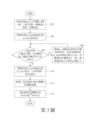
請參照第2圖,其繪示乃依照本揭露一實施例之一種計算模數乘法之方法的流程圖,包括以下步驟。首先,於步驟202,根據一第一運算值A對應之2 iA與目前進行運算之一第二運算值B之m個位元,更新一總和值和一進位值。m為正整數,i為0至m-1之整數。接著,於步驟204,藉由使用一尋找表,記錄與一模數相關的多個數值,並依照總和值選擇此些數值之一作為一尋找表輸出值輸出。之後,進入步驟206,藉由使用一加法單元,根據尋找表輸出值更新總和值和進位值。其中,計算模數乘法之方法係以遞迴的方式,藉由使用第二運算值B之不同的m個位元重複上述步驟以更新總和值和進位值,直到第二運算值B的M個全部位元所對應的運算被執行完畢為止,其中m<M,M為正整數。 Please refer to FIG. 2 , which shows a flow chart of a method for calculating modular multiplication according to an embodiment of the present disclosure, including the following steps. First, in step 202, a sum value and a carry value are updated according to 2 i A corresponding to a first operation value A and m bits of a second operation value B currently being operated. m is a positive integer, and i is an integer from 0 to m-1. Next, in step 204, by using a look-up table, a plurality of values related to a modulus are recorded, and one of these values is selected as a look-up table output value according to the sum value to output. Afterwards, enter step 206, by using an adding unit, update the sum value and the carry value according to the output value of the look-up table. Wherein, the method for calculating the modulus multiplication is in a recursive manner, by using the different m bits of the second operation value B to repeat the above steps to update the sum value and the carry value until M bits of the second operation value B Until the operations corresponding to all the bits are executed, where m<M, M is a positive integer.

請參照第3圖,其繪示依照本揭露另一實施例之一種計算模數乘法之方法的流程圖。首先,於步驟302,接收兩個n位元正整數之輸入值,亦即是第一運算值A與第二運算值B。其中n≦256。當n非為256時,第一運算值A與第二運算值B不足256位元之位元係填充(padding)為0。接著,於步驟304,將總和值D_Sum0與進位值D_Carry0先設成0。之後,進入步驟306,記錄目前之遞迴次數(例如是使用計數器116記錄目前為第幾次之遞迴運算),並判斷目前之遞迴次數是否小於256/m。若是,則執行步驟308;若否,則進入步驟310。其中m為第二運算值B之一次遞迴運算處理的位元數,且256/m為正整數。Please refer to FIG. 3 , which shows a flow chart of a method for calculating modulus multiplication according to another embodiment of the present disclosure. First, in step 302, two input values of n-bit positive integers are received, that is, the first operation value A and the second operation value B. where n≦256. When n is not 256, the bits of the first operation value A and the second operation value B less than 256 bits are filled with 0. Next, in step 304, the sum value D_Sum0 and the carry value D_Carry0 are first set to 0. Afterwards, enter step 306, record the current number of recursions (for example, use the counter 116 to record the current number of recursive operations), and judge whether the current number of recursions is less than 256/m. If yes, go to step 308; if not, go to step 310. Wherein m is the number of bits processed by one recursive operation of the second operation value B, and 256/m is a positive integer.

於步驟308中,係根據(式14)透過(m+1)個進位保持加法器與尋找表,來更新總和值D_Sum與進位值D_Carry。透過:

Figure 02_image131
(式15) In step 308, the sum value D_Sum and the carry value D_Carry are updated through (m+1) carry-hold adders and look-up tables according to (Formula 14). through:
Figure 02_image131
(Formula 15)

其中,P為模數 (

Figure 02_image133
),「>>」為右移運算,「LT」為依照第m個進位保持加法器輸出之D_Sum值,查詢尋找表得到之數值。於(m+1)個進位保持加法器與尋找表執行一次運算,以更新一次總和值D_Sum與進位值D_Carry之後,計數器116記錄的計數值係加1,且第二運算值B係向右移位m個位元。 Among them, P is the modulus (
Figure 02_image133
), ">>" is the right shift operation, "LT" is the D_Sum value output by the mth carry-hold adder, and the value obtained by looking up the look-up table. After (m+1) carry-hold adders and the look-up table perform an operation to update the sum value D_Sum and the carry value D_Carry once, the count value recorded by the counter 116 is incremented by 1, and the second operation value B is shifted to the right Bit m bits.

之後,執行步驟310,於執行了256/m次遞迴運算之後,將總和值D_Sum與進位值D_Carry輸入至進位增值加法器來執行加法運算(亦即是將總和值D_Sum與進位值D_Carry相加),以得到一個暫時的值(第一結果值Rt1)。Afterwards, step 310 is executed, and after performing 256/m recursive operations, the sum value D_Sum and the carry value D_Carry are input to the carry-increase adder to perform the addition operation (that is, the sum value D_Sum and the carry value D_Carry are added ), to obtain a temporary value (the first result value Rt1).

接著,執行步驟312,將第一結果值Rt1進行模數P的模數運算。之後,執行步驟314,得到最終的模數結果,亦即是(第二結果值Rt2

Figure 02_image135
。 Next, step 312 is executed to perform a modulus operation of modulo P on the first result value Rt1. Afterwards, step 314 is executed to obtain the final modulus result, that is (the second result value Rt2
Figure 02_image135
.

請參照第4圖,其繪示依照本揭露之第1圖實施例之模數乘法電路,於m值等於4時之模數乘法電路方塊圖。m為一次遞迴運算處理的位元數。第4圖可以將256位元乘法中遞迴加法的數量降為256/m=64。Please refer to FIG. 4 , which shows a block diagram of the modulus multiplication circuit when the value of m is 4 according to the modulus multiplication circuit of the embodiment in FIG. 1 of the present disclosure. m is the number of bits processed by a recursive operation. Figure 4 can reduce the number of recursive additions in 256-bit multiplication to 256/m=64.

於第4圖中,參數

Figure 02_image137
。而輸入至模數乘法電路400的第一運算值A與第二運算值B分別為兩個n位元正整數,其中n≦256。當n非256位元時,不足256位元之位元填充(padding)為0。第4圖之模數乘法電路400的輸出為256位元正整數,亦即是第二結果值
Figure 02_image139
。 In Figure 4, the parameter
Figure 02_image137
. The first operation value A and the second operation value B input to the modulo-digital multiplication circuit 400 are respectively two n-bit positive integers, where n≦256. When n is not 256 bits, the padding of less than 256 bits is 0. The output of the modulus multiplication circuit 400 in Fig. 4 is a 256-bit positive integer, which is the second result value
Figure 02_image139
.

模數乘法電路400包含元件暫存器422與424,例如分別由D型正反器來實現,用於記錄目前之總和值與進位值的值。多工器418與420用以一開始將儲存於暫存器422與424初始總和值D_Sum0與初始進位值D_Carry0設成0,之後將主要運算電路402輸出之總和值D_Sum與進位值D_Carry依照下列(式16)設成更新的值:

Figure 02_image141
(式16) 其中,數值sum係為目前的總和值(例如是初始總和值D_Sum0),數值carry係為目前的進位值(例如是初始進位值D_Carry0),更新後之總和值D_Sum係為數值sum new,更新後的進位值D_Carry係為數值carry new。於完成一次總和值D_Sum與進位值D_Carry的更新之後,第二運算值B係向右平移4的位元而更新為B new。 The modulus multiplication circuit 400 includes component registers 422 and 424 , which are realized by D-type flip-flops, respectively, and are used to record the current sum value and carry value. The multiplexers 418 and 420 are used to initially set the initial sum value D_Sum0 and the initial carry value D_Carry0 stored in the temporary registers 422 and 424 to 0, and then set the sum value D_Sum and the carry value D_Carry output by the main operation circuit 402 according to the following ( Equation 16) is set to the updated value:
Figure 02_image141
(Formula 16) Among them, the value sum is the current sum value (for example, the initial sum value D_Sum0), the value carry is the current carry value (for example, the initial carry value D_Carry0), and the updated sum value D_Sum is the value sum new , the updated carry value D_Carry is the value carry new . After updating the sum value D_Sum and the carry value D_Carry once, the second operation value B is shifted to the right by 4 bits and updated to B new .

計數器416係用以記錄目前的遞迴次數。為了實現(式16)中的更新,需要透過4個多工器410(0)~410(3)來接收暫存於暫存器434中的第二運算值B的四個位元,以決定是否將2 iA加入目前的總和值(例如是初始總和值D_Sum0)與目前的進位值(例如是初始進位值D_Carry0)。一次遞迴運算處理中,第二運算值B被處理的位元數係為4位元。一次遞迴運算處理完畢後,第二運算值B係藉由移位器436右移4個位元。 The counter 416 is used to record the current recursion times. In order to realize the update in (Formula 16), four multiplexers 410(0)-410(3) need to receive the four bits of the second operation value B temporarily stored in the register 434 to determine Whether to add 2 i A to the current sum value (for example, the initial sum value D_Sum0) and the current carry value (for example, the initial carry value D_Carry0). In one recursive operation process, the number of bits processed by the second operation value B is 4 bits. After one recursive operation is processed, the second operation value B is shifted right by 4 bits by the shifter 436 .

進位保持加法器CSA(1)~CSA(4)將目前的總和值(例如是初始總和值D_Sum0)與目前的進位值(例如是初始進位值D_Carry0)分別根據暫存器R(0)~R(3)所儲存的第二運算值B的四個位元與A、2A、4A、8A進行加法動作,其中2A、4A、8A之值係透過將第一運算值A分別經由移位器412(1)~412(3)之分別向左平移1至3個位元後得到。再透過加法單元406 (另一個進位保持加法器)將查詢尋找表404中與模數P(

Figure 02_image137
)有關的數值(LT),與進位保持加法器CSA(4)輸出之第4個總和運算值Sum(4)與第4個進位運算值Carry(4)相加,以得更新後的總和值D_Carry’和進位值D_Sum’。 The carry-hold adders CSA(1)~CSA(4) combine the current sum value (for example, the initial sum value D_Sum0) and the current carry value (for example, the initial carry value D_Carry0) according to the registers R(0)~R (3) The four bits of the stored second operation value B are added to A, 2A, 4A, and 8A, wherein the values of 2A, 4A, and 8A are obtained by passing the first operation value A through the shifter 412 (1)~412(3) are obtained after shifting 1 to 3 bits to the left respectively. Then through the addition unit 406 (another carry-hold adder) the look-up table 404 and the modulus P (
Figure 02_image137
) related value (LT), add the 4th sum operation value Sum(4) output by the carry-hold adder CSA(4) and the 4th carry operation value Carry(4) to obtain the updated sum value D_Carry' and carry value D_Sum'.

尋找表404記錄2 m(於本例中等於2 4=16)個與P相關的數值,分別為:

Figure 02_image143
,亦即是
Figure 02_image145
,其中
Figure 02_image147
為下取整函數(floor function)。 Look for table 404 to record 2 m (equal to 2 4 =16 in this example) values related to P, respectively:
Figure 02_image143
, that is
Figure 02_image145
,in
Figure 02_image147
is the floor function.

尋找表404會根據第4個進位保持加法器CSA(4)輸出的第4個總和運算值Sum(4)尋找一筆記錄的資料作為尋找表輸出值Lout,亦即作為(式16)之LT值,尋找表輸出值(LT)與第4個進位保持加法器CSA(4)輸出的第4個總和運算值Sum(4)與第4個進位運算值Carry(4)透過加法單元406(可為第5個進位保持加法器)進行相加。The lookup table 404 will look for a record of data according to the fourth sum operation value Sum(4) output by the fourth carry-hold adder CSA(4) as the lookup table output value Lout, that is, as the LT value of (Formula 16) , look for the table output value (LT) and the 4th sum operation value Sum (4) output by the 4th carry-hold adder CSA (4) and the 4th carry operation value Carry (4) through the addition unit 406 (which can be The 5th carry-hold adder) performs the addition.

進位增值加法器426係將經過64次遞迴後得到之總和值D_Sum’與進位值D_Carry’相加,以得到第一結果值Rt1。模數運算器428將第一結果值Rt1進行模數P(

Figure 02_image137
)運算,得第二結果值Rt2(
Figure 02_image139
)。 The carry-increment adder 426 adds the sum value D_Sum′ obtained after 64 iterations to the carry value D_Carry′ to obtain the first result value Rt1. The modulus operator 428 modulus P(
Figure 02_image137
) operation, get the second result value Rt2(
Figure 02_image139
).

本揭露利用上述蒙哥馬利演算法降低模數運算的複雜性,並在不使用記憶體的前提下利用進位保持加法器將256位元乘法中之遞迴加法處理的數量降至64次(此以本揭露之實施例m=4為例,m為一次遞迴運算處理的位元數)。本揭露可僅透過加法器、多工器、移位器等電路元件,即可完成複雜的模數乘法之運算,可以省去複雜的乘法電路,而達到節省電路面積與降低能量損耗的功效。本揭露更同時可提升時脈頻率,而提升電路的處理速度。This disclosure utilizes the aforementioned Montgomery algorithm to reduce the complexity of modulus operations, and uses a carry-hold adder to reduce the number of recursive additions in 256-bit multiplication to 64 times without using memory In the disclosed embodiment m=4 as an example, m is the number of bits processed by one recursive operation). In the present disclosure, complex modulus multiplication operations can be completed only through circuit elements such as adders, multiplexers, and shifters, and complex multiplication circuits can be omitted, thereby achieving the effects of saving circuit area and reducing energy consumption. The present disclosure can increase the clock frequency at the same time, thereby increasing the processing speed of the circuit.

本揭露需預處理資料僅為與模數P有關的多個數值(亦即是尋找表中的與模數P相關的多個數值),預處理資料不需隨被乘數與乘數而有所變動。因此,對於固定模數P的模數乘法電路而言,本揭露的預處理資料之尋找表的內容可以利用電路上的真值表、解碼器、或其他組合邏輯電路來實現,而不需要使用到額外的暫存器與記憶體,解決了其他相關先前技術之需要計算預處理資料的問題。The preprocessing data required in this disclosure are only multiple values related to the modulus P (that is, to find multiple values related to the modulus P in the table), and the preprocessing data does not need to be related to the multiplicand and the multiplier changed. Therefore, for the modulus multiplication circuit with a fixed modulus P, the content of the look-up table of the preprocessing data disclosed in the present disclosure can be realized by using a truth table, a decoder, or other combinational logic circuits on the circuit, without using The additional register and memory solves the problem of calculating preprocessed data in other related prior art.

總而言之,本實施所能達到效果包括:(一)不需使用記憶儲存單元:由於尋找表的內容僅與參數P有關,故可由電路上的真值表、解碼器、或其他組合邏輯電路來實現,而不用額外的記憶儲存單元。(二)提升運算速度: 藉由進位保持加法器可縮短關鍵長度並降低遞迴數量,可增加時脈頻率並提升運算速度。(三)低功耗:由於不需要記憶儲存單元,且核心遞迴由進位保持加法器完成,可降低執行時的能量消耗。本揭露之實施例在m=4時,能有良好之上述之功效。In a word, the effect that this implementation can achieve includes: (1) no need to use the memory storage unit: because the content of the look-up table is only relevant to the parameter P, it can be realized by a truth table on the circuit, a decoder, or other combinational logic circuits , without an additional memory storage unit. (2) Improving operation speed: By using the carry-hold adder, the key length can be shortened and the number of recursions can be reduced, the clock frequency can be increased and the operation speed can be increased. (3) Low power consumption: Since no memory storage unit is required, and the core recursion is completed by a carry-hold adder, energy consumption during execution can be reduced. The embodiment of the present disclosure can have good above-mentioned effects when m=4.

茲將本揭露之實施例的功效與以下之先前技術一至先前技術四進行比較。The efficacy of the embodiment of the present disclosure is compared with the following prior art 1 to prior art 4.

先前技術一: M. A. Mehrabi and C. Doche, “Low-Cost, Low-Power FPGA Implementation of ED25519 and CURVE25519 Point Multiplication,” Information, vol. 10, no. 9, p. 285, 2019. Prior Art 1: MA Mehrabi and C. Doche, “Low-Cost, Low-Power FPGA Implementation of ED25519 and CURVE25519 Point Multiplication,” Information , vol. 10, no. 9, p. 285, 2019.

先前技術二:Rahimzadeh, L.; Eshghi, M.; Timarchi, S. Radix-4 implementation of redundant interleaved modular multiplication on FPGA. In Proceedings of the 2014 22nd Iranian Conference on Electrical Engineering (ICEE), Tehran, Iran, 20–22 May 2014; pp. 523–526.Prior Art 2: Rahimzadeh, L.; Eshghi, M.; Timarchi, S. Radix-4 implementation of redundant interleaved modular multiplication on FPGA. In Proceedings of the 2014 22nd Iranian Conference on Electrical Engineering (ICEE), Tehran, Iran, 20 –22 May 2014; pp. 523–526.

先前技術三: Javeed, K.; Wang, X. Radix-4 and radix-8 booth encoded interleaved modular multipliers over general Fp. In Proceedings of the 2014 24th International Conference on Field Programmable Logic and Applications (FPL), Munich, Germany, 2–4 September 2014.Prior Art 3: Javeed, K.; Wang, X. Radix-4 and radix-8 booth encoded interleaved modular multipliers over general Fp. In Proceedings of the 2014 24th International Conference on Field Programmable Logic and Applications (FPL), Munich, Germany , 2–4 September 2014.

先前技術四:Nassar, M.A.; El-Sayed, L.A. Efficient Interleaved Modular Multiplication Based on Sign Detection. In Proceedings of the 2015 IEEE/ACS 12th International Conference of Computer Systems and Applications (AICCSA), Marrakech, Morocco, 17–20 November 2015.Prior Art 4: Nassar, M.A.; El-Sayed, L.A. Efficient Interleaved Modular Multiplication Based on Sign Detection. In Proceedings of the 2015 IEEE/ACS 12th International Conference of Computer Systems and Applications (AICCSA), Marrakech, Morocco, 17–20 November 2015.

先前技術一為使用基數8之交錯模數乘法(Radix-8 interleaved modulo multiplication)。先前技術一的缺點在於,每次進行計算前都需要進行資料的預處理,同時需要額外的記憶體以記錄預處理的資料。先前技術二與先前技術一類似,差別在於使用基數4(Radix-4)而非基數8(Radix-8)。雖然使得預處理的資料較少,但卻增加了在256位元乘法中遞迴加法的數量。先前技術三並無對資料進行預處理,使得該架構的關鍵長度較長,時脈頻率較低。先前技術四則使用EIMM(Efficient Interleaved Modular Multiplication Based on Sign Detection)演算法,藉由符號偵測(Sign detection)技巧減低模數運算的複雜度。然而其256位元乘法中遞迴加法的次數卻並沒有減少,而是維持原本的256次,使得整體運算量較多。Prior art one is to use radix-8 interleaved modulo multiplication (Radix-8 interleaved modulo multiplication). The disadvantage of the prior technique 1 is that data preprocessing is required before each calculation, and additional memory is required to record the preprocessed data. The prior art 2 is similar to the prior art 1, except that a radix 4 (Radix-4) is used instead of a radix 8 (Radix-8). While this results in less preprocessing data, it increases the number of recursive additions in the 256-bit multiplication. The prior art 3 does not preprocess the data, so the key length of the architecture is longer and the clock frequency is lower. The fourth prior art uses the EIMM (Efficient Interleaved Modular Multiplication Based on Sign Detection) algorithm to reduce the complexity of the modulus calculation by means of the sign detection technique. However, the number of recursive additions in the 256-bit multiplication has not been reduced, but the original 256 times has been maintained, which makes the overall calculation amount larger.

本揭露實施例與型號Ed25519相關的低功耗模數乘法架構之上述之先前技術一至四進行比較,其結果如以下表一所示。本揭露實施例與先前技術一至四皆可實現型號Ed25519中的模術乘法運算。於表一中,係列出了本揭露之m值等於4之第一實施例、本揭露之m值等於8之第二實施例、先前技術一至四之運算平台(Compute Platform)、延遲(Latency)、時脈頻率(Clock Frequency)與功率(Power)之比較。由表一可以看出,本揭露之第一實施例與第二實施例所損耗之功率相較於先前技術一至四降低很多,確實具有低功率損耗之特性。   運算平台 延遲 (ns) 時脈頻率 (MHz) 功率 (mW) 第一實施例 ASIC (40-nm) 136 500 8.4 第二實施例 ASIC (40-nm) 72 500 9.9 先前技術一 ZYNQ7000(FPGA, 28-nm PL) 180 550 152 先前技術二 VIRTEX5 (FPGA, 65-nm PL) 303 442 2311 先前技術三 VIRTEX6 (FPGA, 40-nm PL) 1487 86.6 2319 先前技術四 VIRTEX4 (FPGA, 90-nm PL) 1171.66 437.12 2556 表一 The disclosed embodiment is compared with the above-mentioned prior art 1 to 4 of the low-power modulus multiplication architecture related to the model Ed25519, and the results are shown in Table 1 below. The embodiment of the present disclosure and the prior art 1 to 4 can realize the modular multiplication operation in the model Ed25519. In Table 1, the first embodiment in which the value of m in this disclosure is equal to 4, the second embodiment in which the value of m in this disclosure is equal to 8, the computing platforms (Compute Platform) and delay (Latency) of prior art 1 to 4 are listed in series. , Clock Frequency (Clock Frequency) and power (Power) comparison. It can be seen from Table 1 that the power loss of the first embodiment and the second embodiment of the present disclosure is much lower than that of the prior art 1 to 4, and indeed has the characteristic of low power loss. computing platform delay (ns) Clock Frequency(MHz) Power (mW) first embodiment ASICs (40-nm) 136 500 8.4 second embodiment ASICs (40-nm) 72 500 9.9 Prior art one ZYNQ7000 (FPGA, 28-nm PL) 180 550 152 Prior Art II VIRTEX5 (FPGA, 65-nm PL) 303 442 2311 Prior Art Three VIRTEX6 (FPGA, 40-nm PL) 1487 86.6 2319 Prior Art Four VIRTEX4 (FPGA, 90-nm PL) 1171.66 437.12 2556 Table I

綜上所述,雖然本揭露已以實施例揭露如上,然其並非用以限定本揭露。本揭露所屬技術領域中具有通常知識者,在不脫離本揭露之精神和範圍內,當可作各種之更動與潤飾。因此,本揭露之保護範圍當視後附之申請專利範圍所界定者為準。To sum up, although the present disclosure has been disclosed above with embodiments, it is not intended to limit the present disclosure. Those with ordinary knowledge in the technical field to which this disclosure belongs may make various changes and modifications without departing from the spirit and scope of this disclosure. Therefore, the scope of protection of this disclosure should be defined by the scope of the appended patent application.

100,400:模數乘法電路 102,402:主要運算電路 104,404:尋找表 106,406:加法單元 108,408:乘法運算電路 110(0)~110(m-1),410(0)~410(3),118,120,418,420:多工器 112(1)~112(m-1),130,132,136,412(1)~412(3),430,432,436:移位器 114,414:加法運算電路 116,416:計數器 122,124,134,422,424,434:暫存器 126,426:進位增值加法器 128,428:模數運算器 202~206,302~314:流程步驟 100,400: modulus multiplication circuit 102,402: Main operation circuit 104, 404: lookup table 106,406: Addition unit 108,408: Multiplication circuit 110(0)~110(m-1),410(0)~410(3),118,120,418,420: multiplexer 112(1)~112(m-1),130,132,136,412(1)~412(3),430,432,436: shifter 114,414: Addition circuit 116,416: counter 122,124,134,422,424,434: scratchpad 126,426: Carry value-added adder 128,428: modulus operator 202~206,302~314: process steps

第1圖繪示依照本揭露一實施例之一種模數乘法電路之方塊圖; 第2圖繪示依照本揭露一實施例之一種計算模數乘法之方法的流程圖; 第3圖繪示依照本揭露另一實施例之一種計算模數乘法之方法的流程圖;及 第4圖繪示依照本揭露之第1圖實施例之模數乘法電路,於m值等於4時之模數乘法電路方塊圖。 FIG. 1 shows a block diagram of a modular multiplication circuit according to an embodiment of the present disclosure; FIG. 2 shows a flow chart of a method for calculating modulus multiplication according to an embodiment of the present disclosure; FIG. 3 shows a flow chart of a method for calculating modular multiplication according to another embodiment of the present disclosure; and FIG. 4 shows a block diagram of the modulus multiplication circuit when the value of m is 4 according to the modulus multiplication circuit of the embodiment of FIG. 1 of the present disclosure.

100:模數乘法電路 100: Modulus multiplication circuit

102:主要運算電路 102: Main operation circuit

104:尋找表 104: Find table

106:加法單元 106: Addition unit

108:乘法運算電路 108: Multiplication operation circuit

110(0)~110(m-1),118,120:多工器 110(0)~110(m-1),118,120: multiplexer

112(1)~112(m-1),130,132,136:移位器 112(1)~112(m-1),130,132,136: shifter

114:加法運算電路 114: Addition operation circuit

116:計數器 116: Counter

122,124,134:暫存器 122,124,134: scratchpad

126:進位增值加法器 126: Carry value-added adder

128:模數運算器 128: Modulus operator

Claims (20)

一種模數乘法電路,包括: 一主要運算電路,用以根據一第一運算值A對應之2 iA與目前進行運算之一第二運算值B之m個位元,更新一總和值和一進位值,m為正整數,i為0至m-1之整數; 一尋找表,用以記錄與一模數相關的複數個數值,並依照該總和值選擇該些數值之一作為一尋找表輸出值輸出;以及 一加法單元,用以根據該尋找表輸出值更新該總和值和該進位值,並輸出至該主要運算電路; 其中,該模數乘法電路係以遞迴的方式,藉由使用該第二運算值B之不同的m個位元,來進行上述運算以更新該總和值和該進位值,直到該第二運算值B的M個全部位元所對應的運算被執行完畢為止,其中m<M,M為正整數。 A modulo-digital multiplication circuit, comprising: a main operation circuit, used to update a sum value and a value according to 2 i A corresponding to a first operation value A and m bits of a second operation value B currently being operated. carry value, m is a positive integer, i is an integer from 0 to m-1; a look-up table, used to record complex values related to a modulus, and select one of these values according to the sum value as a look-up table Output value output; and an addition unit, used to update the sum value and the carry value according to the output value of the look-up table, and output to the main operation circuit; wherein, the modulus multiplication circuit is in a recursive manner, by Use the different m bits of the second operation value B to perform the above operation to update the sum value and the carry value until the operations corresponding to all the M bits of the second operation value B are executed. , where m<M, M is a positive integer. 如請求項1所述之模數乘法電路,其中該主要運算電路係計算目前進行運算之該第二運算值B之m個位元之各個位元,與對應之2 iA之乘積之和,以更新該總和值和該進位值。 The modulus multiplication circuit as described in claim 1, wherein the main operation circuit is to calculate the sum of the products of the m bits of the second operation value B currently being operated and the corresponding 2 i A, to update the sum value and the carry value. 如請求項1所述之模數乘法電路,其中該主要運算電路包括: 一乘法運算電路,包括一第0個多工器至一第m-1個多工器與一第0個暫存器至一第m-1個暫存器,該第0個暫存器至該第m-1個暫存器係各自儲存目前進行運算之該第二運算值B之m個位元之一,該第0個多工器至該第m-1個多工器之選擇端係分別受控於該第0個暫存器至該第m-1個暫存器之輸出值,該第0個多工器至該第m-1個多工器之第一輸入端係接收數位值0,該第0個多工器至該第m-1個多工器之第二輸入端係分別接收2 0A至2 m-1A,該總和值與該進位值係由該第0個多工器至該第m-1個多工器之輸出值所決定; 其中,於該第二運算值B之該m個位元所對應的運算被執行完畢之後,該第0個暫存器至該第m-1個暫存器係分別儲存接著將進行運算之該第二運算值B之另外m個位元,以重複執行上述動作。 The modulus multiplication circuit as described in claim 1, wherein the main operation circuit includes: a multiplication operation circuit including a 0th multiplexer to an m-1th multiplexer and a 0th temporary register To an m-1th temporary register, the 0th temporary register to the m-1th temporary register are each storing one of the m bits of the second calculation value B currently performing calculations, the The selection terminals of the 0th multiplexer to the m-1th multiplexer are respectively controlled by the output values of the 0th register to the m-1th register, and the 0th multiplexer The first input terminal of the multiplexer to the m-1th multiplexer is to receive a digital value 0, and the second input terminal of the 0th multiplexer to the m-1th multiplexer is to receive 2 0 respectively A to 2 m-1 A, the sum value and the carry value are determined by the output values of the 0th multiplexer to the m-1th multiplexer; wherein, in the second operation value B After the operation corresponding to the m bits is executed, the 0th register to the m-1th register respectively store the other m bits of the second operation value B to be operated on element to repeat the above actions. 如請求項3所述之模數乘法電路,其中2 0A至2 m-1A係藉由使該第一運算值A分別向左移位(shift left)0至m-1個位元來實現。 The modulus multiplication circuit as described in claim 3, wherein 2 0 A to 2 m-1 A are obtained by shifting the first operation value A to the left by 0 to m-1 bits respectively accomplish. 如請求項3所述之模數乘法電路,其中該主要運算電路更包括: 一加法運算電路,包括一第1個進位保持加法器(Carry save adder, CSA)至一第m個進位保持加法器,該第1個進位保持加法器係接收一初始總和運算值Sum(0)、一初始進位運算值Carry(0)、與該第0個多工器之輸出值,並輸出一第1個總和運算值Sum(1)與一第1個進位運算值Carry(1),該第2個進位保持加法器係接收該第1個總和運算值Sum(1)、該第1個進位運算值Carry(1)、與該第1個多工器之輸出值,並輸出一第2個總和運算值Sum(2)與一第2個進位運算值Carry(2),該第m個進位保持加法器係接收一第m-1個總和運算值Sum(m-1)、一第m-1個進位運算值Carry(m-1)、與該第m-1個多工器之輸出值,並輸出一第m個總和運算值Sum(m)與一第m個進位運算值Carry(m),該第m個總和運算值Sum(m)與該第m個進位運算值Carry(m)係作為該主要運算電路輸出之該總和值和該進位值。 The modulus multiplication circuit as described in claim 3, wherein the main operation circuit further includes: An addition operation circuit, including a first carry save adder (Carry save adder, CSA) to an mth carry save adder, the first carry save adder receives an initial sum operation value Sum(0) , an initial carry operation value Carry(0), and the output value of the 0th multiplexer, and output a first sum operation value Sum(1) and a first carry operation value Carry(1), the The second carry-hold adder receives the first sum operation value Sum(1), the first carry operation value Carry(1), and the output value of the first multiplexer, and outputs a second A sum operation value Sum(2) and a 2nd carry operation value Carry(2), the m-th carry-hold adder receives an m-1th sum operation value Sum(m-1), an m-th operation value Sum(m-1), -1 carry operation value Carry(m-1), and the output value of the m-1th multiplexer, and output an m-th sum operation value Sum(m) and an m-th carry operation value Carry( m), the m th sum operation value Sum(m) and the m th carry operation value Carry(m) are used as the sum value and the carry value output by the main operation circuit. 如請求項3所述之模數乘法電路,其中於該第二運算值B之該m個位元所對應的運算被執行完畢之後,該加法單元輸出之更新後的該總和值和該進位值係向右移位(shift right)m個位元後,輸入至該主要運算電路,該第二運算值B係向右移位m個位元後,取m個位元作為儲存於該第0個暫存器至該第m-1個暫存器之接著將進行運算之該第二運算值B之另外m個位元。The modulus multiplication circuit as described in claim 3, wherein after the operation corresponding to the m bits of the second operation value B is executed, the updated sum value and the carry value output by the adding unit After being shifted to the right by m bits, it is input to the main operation circuit. After the second operation value B is shifted to the right by m bits, m bits are taken as being stored in the 0th bit. The other m bits of the second operation value B to be operated next from the first register to the m-1th register. 如請求項1所述之模數乘法電路,其中該尋找表係記錄與該模數相關的2 m個數值,該2 m個數值係各自可被2 m整除,該尋找表係透過一組合邏輯電路實現,該加法單元係將該主要運算電路輸出之該總和值和該進位值與該尋找表輸出值相加,以輸出更新後之該總和值和該進位值。 The modulus multiplication circuit as described in claim 1, wherein the look-up table records 2 m values related to the modulus, and the 2 m values are each divisible by 2 m , and the look-up table is passed through a combinational logic Circuit implementation, the adding unit adds the sum value and the carry value output by the main operation circuit to the output value of the look-up table to output the updated sum value and the carry value. 如請求項1所述之模數乘法電路,更包括: 一進位增值加法器(Carry propagate adder, CPA),用以於該第二運算值B的M個全部位元所對應的運算被執行完畢時,將更新後的該總和值與該進位值相加,以得到一第一結果值;以及 一模數運算器(Mod operator),用以將該第一結果值進行模數運算,以得到一第二結果值,並以該第二結果值作為該模數乘法電路之輸出。 The modulus multiplication circuit as described in claim 1 further includes: A Carry propagate adder (CPA), used for adding the updated sum value to the carry value when the operations corresponding to all M bits of the second operation value B are executed , to obtain a first result value; and A modulus operator (Mod operator) is used to perform modulus operation on the first result value to obtain a second result value, and use the second result value as the output of the modulo multiplication circuit. 如請求項1所述之模數乘法電路,其中該尋找表係記錄與該模數相關的2 m個值,與該模數相關的該2 m個數值包括
Figure 03_image149
,其中
Figure 03_image147
為下取整函數(floor function)。
The modulus multiplication circuit as described in claim 1, wherein the look-up table records 2 m values related to the modulus, and the 2 m values related to the modulus include
Figure 03_image149
,in
Figure 03_image147
is the floor function.
如請求項1所述之模數乘法電路,其中該尋找表係包括一組合邏輯電路(Combinational logic),藉由使該組合邏輯電路之至少一端點電性耦接至一高電位或一低電位,來記錄與該模數相關的該些數值,並藉由該組合邏輯電路得到與輸入至該尋找表之該總和值對應之與該模數相關的該些數值之一。The modulus multiplication circuit as described in Claim 1, wherein the look-up table includes a combinational logic circuit (Combinational logic), by electrically coupling at least one terminal of the combinational logic circuit to a high potential or a low potential , to record the numerical values related to the modulus, and obtain one of the numerical values related to the modulus corresponding to the sum value input to the look-up table through the combinational logic circuit. 一種計算模數乘法之方法,包括: 根據一第一運算值A對應之2 iA與目前進行運算之一第二運算值B之m個位元,更新一總和值和一進位值,m為正整數,i為0至m-1之整數; 藉由使用一尋找表,記錄與一模數相關的複數個數值,並依照該總和值選擇該些數值之一作為一尋找表輸出值輸出;以及 藉由使用一加法單元,根據該尋找表輸出值更新該總和值和該進位值; 其中,該計算模數乘法之方法係以遞迴的方式,藉由使用該第二運算值B之不同的m個位元,來重複上述步驟以更新該總和值和該進位值,直到該第二運算值B的M個全部位元所對應的運算被執行完畢為止,其中m<M,M為正整數。 A method for calculating modulus multiplication, comprising: updating a sum value and a carry value according to 2 i A corresponding to a first operation value A and m bits of a second operation value B currently being operated, where m is A positive integer, i is an integer from 0 to m-1; by using a look-up table, recording complex values related to a modulus, and selecting one of these values according to the sum value as a look-up table output value output; and updating the sum value and the carry value according to the output value of the look-up table by using an adding unit; wherein, the method of calculating the modulo multiplication is in a recursive manner, by using the difference of the second operation value B Repeat the above steps to update the sum value and the carry value until the operation corresponding to all the M bits of the second operation value B is executed, where m<M, M is positive integer. 如請求項11所述之計算模數乘法之方法,其中,係藉由計算目前進行運算之該第二運算值B之m個位元之各個位元,與對應之2 iA之乘積之和,以更新該總和值和該進位值。 The method for calculating modulus multiplication as described in claim 11, wherein, by calculating the sum of the products of the m bits of the second operation value B currently being operated and the corresponding 2 i A , to update the sum value and the carry value. 如請求項11所述之計算模數乘法之方法,其中,根據該第一運算值A對應之2 iA與目前進行運算之該第二運算值B之m個位元,更新該總和值和該進位值之步驟,係藉由一主要運算電路來完成,該主要運算電路包括: 一乘法運算電路,包括一第0個多工器至一第m-1個多工器與一第0個暫存器至一第m-1個暫存器,該第0個暫存器至該第m-1個暫存器係各自儲存目前進行運算之該第二運算值B之m個位元之一,該第0個多工器至該第m-1個多工器之選擇端係分別受控於該第0個暫存器至該第m-1個暫存器之輸出值,該第0個多工器至該第m-1個多工器之第一輸入端係接收數位值0,該第0個多工器至該第m-1個多工器之第二輸入端係分別接收2 0A至2 m-1A,該總和值與該進位值係由該第0個多工器至該第m-1個多工器之輸出值所決定; 其中,於該第二運算值B之該m個位元所對應的運算被執行完畢之後,該第0個暫存器至該第m-1個暫存器係分別儲存接著將進行運算之該第二運算值B之另外m個位元,以重複執行上述動作。 The method for calculating modulus multiplication as described in claim 11, wherein, according to the m bits of 2 i A corresponding to the first operation value A and the second operation value B currently being operated, update the sum value and The step of the carry value is accomplished by a main operation circuit, which includes: a multiplication operation circuit, including a 0th multiplexer to an m-1th multiplexer and a 0th multiplexer register to an m-1th register, the 0th register to the m-1th register are respectively storing the m bits of the second operation value B currently performing operations 1. The selection terminals of the 0th multiplexer to the m-1th multiplexer are respectively controlled by the output values of the 0th register to the m-1th register. The first input terminals of the 0th multiplexer to the m-1th multiplexer receive a digital value 0, and the second input terminals of the 0th multiplexer to the m-1th multiplexer are respectively Receive 2 0 A to 2 m-1 A, the sum value and the carry value are determined by the output values of the 0th multiplexer to the m-1th multiplexer; wherein, in the second operation After the operation corresponding to the m bits of the value B is executed, the 0th register to the m-1th register are respectively stored in addition to the second operation value B to be operated next. m bits to repeat the above actions. 如請求項13所述之計算模數乘法之方法,其中2 0A至2 m-1A係藉由使該第一運算值A分別向左移位0至m-1個位元來實現。 The method for calculating modulus multiplication as described in Claim 13, wherein 2 0 A to 2 m-1 A are realized by shifting the first operation value A to the left by 0 to m-1 bits respectively. 如請求項13所述之計算模數乘法之方法,其中該主要運算電路更包括: 一加法運算電路,包括一第1個進位保持加法器至一第m個進位保持加法器,該第1個進位保持加法器係接收一初始總和運算值Sum(0)、一初始進位運算值Carry(0)、與該第0個多工器之輸出值,並輸出一第1個總和運算值Sum(1)與一第1個進位運算值Carry(1),該第2個進位保持加法器係接收該第1個總和運算值Sum(1)、該第1個進位運算值Carry(1)、與該第1個多工器之輸出值,並輸出一第2個總和運算值Sum(2)與一第2個進位運算值Carry(2),該第m個進位保持加法器係接收一第m-1個總和運算值Sum(m-1)、一第m-1個進位運算值Carry(m-1)、與該第m-1個多工器之輸出值,並輸出一第m個總和運算值Sum(m)與一第m個進位運算值Carry(m),該第m個總和運算值Sum(m)與該第m個進位運算值Carry(m)係作為該主要運算電路輸出之該總和值和該進位值。 The method for calculating modulus multiplication as described in Claim 13, wherein the main operation circuit further includes: An addition operation circuit, comprising a first carry-hold adder to an m-th carry-hold adder, the first carry-hold adder receives an initial sum operation value Sum(0), an initial carry operation value Carry (0), and the output value of the 0th multiplexer, and output a first sum operation value Sum(1) and a first carry operation value Carry(1), the second carry hold adder It receives the first sum operation value Sum(1), the first carry operation value Carry(1), and the output value of the first multiplexer, and outputs a second sum operation value Sum(2 ) and a 2nd carry operation value Carry(2), the m-th carry hold adder receives an m-1th sum operation value Sum(m-1), an m-1th carry operation value Carry (m-1), and the output value of the m-1 multiplexer, and output an m-th sum operation value Sum(m) and an m-th carry operation value Carry(m), the m-th The sum operation value Sum(m) and the mth carry operation value Carry(m) are the sum value and the carry value output by the main operation circuit. 如請求項13所述之計算模數乘法之方法,其中於該第二運算值B之該m個位元所對應的運算被執行完畢之後,該加法單元輸出之更新後的該總和值和該進位值係向右移位m個位元後,輸入至該主要運算電路,該第二運算值B係向右移位m個位元後,取m個位元作為儲存於該第0個暫存器至該第m-1個暫存器之接著將進行運算之該第二運算值B之另外m個位元。The method for calculating modulus multiplication as described in claim 13, wherein after the operation corresponding to the m bits of the second operation value B is executed, the updated sum value output by the adding unit and the The carry value is shifted to the right by m bits, and then input to the main operation circuit, and the second operation value B is shifted to the right by m bits, and m bits are taken as being stored in the 0th temporary The other m bits of the second operation value B to be operated next from the register to the m-1th temporary register. 如請求項11所述之計算模數乘法之方法,其中該尋找表係記錄與該模數相關的2 m個數值,該2 m個數值係各自可被2 m整除,該尋找表係透過一組合邏輯電路實現,該加法單元係將該主要運算電路輸出之該總和值和該進位值與該尋找表輸出值相加,以輸出更新後之該總和值和該進位值。 The method for calculating the multiplication of a modulus as described in claim 11, wherein the look-up table records 2 m values related to the modulus, and the 2 m values are each divisible by 2 m , and the look-up table is passed through a The combinational logic circuit realizes that the adding unit adds the sum value and the carry value output by the main operation circuit to the output value of the look-up table to output the updated sum value and the carry value. 如請求項11所述之計算模數乘法之方法,更包括: 於該第二運算值B的M個全部位元所對應的運算被執行完畢時,將更新後的該總和值與該進位值相加,以得到一第一結果值;以及 將該第一結果值進行模數運算,以得到一第二結果值,並以該第二結果值作為該模數乘法電路之輸出。 The method for calculating modulus multiplication as described in Claim 11 further includes: When the operation corresponding to all M bits of the second operation value B is completed, add the updated sum value and the carry value to obtain a first result value; and The modulus operation is performed on the first result value to obtain a second result value, and the second result value is used as the output of the modulus multiplication circuit. 如請求項11所述之計算模數乘法之方法,其中該尋找表係記錄與該模數相關的2 m個值,包括
Figure 03_image149
,其中
Figure 03_image147
為下取整函數。
The method for calculating modulus multiplication as described in claim 11, wherein the look-up table records 2 m values related to the modulus, including
Figure 03_image149
,in
Figure 03_image147
is the lower integer function.
如請求項11所述之計算模數乘法之方法,其中該尋找表係包括一組合邏輯電路,藉由使該組合邏輯電路之至少一端點電性耦接至一高電位或一低電位,來記錄與該模數相關的該些數值,並藉由該組合邏輯電路得到與輸入至該尋找表之該總和值對應之與該模數相關的該些數值之一。The method for calculating modulus multiplication as described in claim 11, wherein the look-up table includes a combinational logic circuit, by electrically coupling at least one terminal of the combinational logic circuit to a high potential or a low potential to The numerical values related to the modulus are recorded, and one of the numerical values related to the modulus corresponding to the sum value input to the look-up table is obtained through the combinational logic circuit.
TW110143399A 2021-11-22 2021-11-22 Modular multiplication circuit and corresponding modular multiplication method TWI802095B (en)

Priority Applications (3)

Application Number Priority Date Filing Date Title
TW110143399A TWI802095B (en) 2021-11-22 2021-11-22 Modular multiplication circuit and corresponding modular multiplication method
CN202111547064.XA CN116149605A (en) 2021-11-22 2021-12-16 Modulus Multiplication Circuit and Method for Calculating Modulus Multiplication
US17/562,793 US11829731B2 (en) 2021-11-22 2021-12-27 Modular multiplication circuit and corresponding modular multiplication method

Applications Claiming Priority (1)

Application Number Priority Date Filing Date Title
TW110143399A TWI802095B (en) 2021-11-22 2021-11-22 Modular multiplication circuit and corresponding modular multiplication method

Publications (2)

Publication Number Publication Date
TWI802095B TWI802095B (en) 2023-05-11
TW202321900A true TW202321900A (en) 2023-06-01

Family

ID=86351246

Family Applications (1)

Application Number Title Priority Date Filing Date
TW110143399A TWI802095B (en) 2021-11-22 2021-11-22 Modular multiplication circuit and corresponding modular multiplication method

Country Status (3)

Country Link
US (1) US11829731B2 (en)
CN (1) CN116149605A (en)
TW (1) TWI802095B (en)

Families Citing this family (1)

* Cited by examiner, † Cited by third party
Publication number Priority date Publication date Assignee Title
CN118233094B (en) * 2024-04-17 2024-09-20 华中科技大学 A modular multiplication circuit suitable for post-quantum cryptographic algorithm Dilithium

Family Cites Families (24)

* Cited by examiner, † Cited by third party
Publication number Priority date Publication date Assignee Title
ES2293677T3 (en) 1997-05-04 2008-03-16 Sandisk Il Ltd IMPROVED APPLIANCE AND METHOD FOR MODULAR MULTIPLICATION AND EXPOSURE BASED ON MONTGOMERY MULTIPLICATION.
US6973470B2 (en) * 2001-06-13 2005-12-06 Corrent Corporation Circuit and method for performing multiple modulo mathematic operations
US7627114B2 (en) * 2002-10-02 2009-12-01 International Business Machines Corporation Efficient modular reduction and modular multiplication
KR100484487B1 (en) 2002-10-29 2005-04-20 한국전자통신연구원 Apparatus and method for modular calculation, and system for calculating Rivest-Shamir-Adleman cryptograph using the apparatus
KR100481586B1 (en) 2002-11-22 2005-04-08 한국전자통신연구원 Apparatus for modular multiplication
KR100459732B1 (en) * 2002-12-30 2004-12-03 삼성전자주식회사 Montgomery modular multiplier by 4 to 2 compressor and multiplication method thereof
KR100458031B1 (en) 2003-03-14 2004-11-26 삼성전자주식회사 Apparatus and method for performing a montgomery type modular multiplication
JP2004326112A (en) 2003-04-25 2004-11-18 Samsung Electronics Co Ltd Multiple modulus selector, accumulator, Montgomery multiplier, multiple modulus generation method, partial multiplication generation method, accumulation method, multiplication method, modulus selector, and booth recorder
JP2004334212A (en) 2003-05-09 2004-11-25 Samsung Electronics Co Ltd Montgomery multiplier and multiplication method
US8194855B2 (en) 2003-06-30 2012-06-05 Oracle America, Inc. Method and apparatus for implementing processor instructions for accelerating public-key cryptography
KR20050088506A (en) 2004-03-02 2005-09-07 삼성전자주식회사 Scalable montgomery modular multiplier supporting multiple precision
KR100836737B1 (en) 2005-12-13 2008-06-10 한국전자통신연구원 Apparatus and method for modular multiplication using chhinese remainder theorem and carry save adder
US7805479B2 (en) 2006-03-28 2010-09-28 Michael Andrew Moshier Scalable, faster method and apparatus for montgomery multiplication
KR20080050226A (en) 2006-12-01 2008-06-05 한국전자통신연구원 Modular multiplication device and design method
KR100946256B1 (en) 2007-12-26 2010-03-08 대구대학교 산학협력단 Scalable Mongolian multiplier on dual field using multi-precision carry save adder
CN101304312B (en) 2008-06-26 2011-07-20 复旦大学 Ciphering unit being suitable for compacting instruction set processor
US8386546B2 (en) * 2009-02-27 2013-02-26 George Mason Intellectual Properties, Inc. Montgomery multiplication architecture
US8433736B2 (en) * 2009-02-27 2013-04-30 George Mason Intellectual Properties, Inc. Scalable Montgomery multiplication architecture
TWI406548B (en) 2010-10-27 2013-08-21 Univ Southern Taiwan An elliptic curve cryptography operation circuit
FR2974201B1 (en) 2011-04-18 2013-04-12 Inside Secure MONTGOMERY MULTIPLICATION CIRCUIT
US9779359B2 (en) 2012-03-14 2017-10-03 Microsoft Technology Licensing, Llc Quantum arithmetic on two-dimensional quantum architectures
CN103914277B (en) 2014-04-14 2017-02-15 复旦大学 Extensible modular multiplier circuit based on improved Montgomery modular multiplication algorithm
US10817262B2 (en) * 2018-11-08 2020-10-27 Enveil, Inc. Reduced and pipelined hardware architecture for Montgomery Modular Multiplication
US11249726B2 (en) * 2019-09-10 2022-02-15 Intel Corporation Integrated circuits with modular multiplication circuitry

Also Published As

Publication number Publication date
US11829731B2 (en) 2023-11-28
US20230168863A1 (en) 2023-06-01
CN116149605A (en) 2023-05-23
TWI802095B (en) 2023-05-11

Similar Documents

Publication Publication Date Title
US20030140077A1 (en) Logic circuits for performing modular multiplication and exponentiation
Gokhale et al. Design of area and delay efficient Vedic multiplier using Carry Select Adder
Liu et al. High performance modular multiplication for SIDH
Timarchi et al. Arithmetic circuits of redundant SUT-RNS
Savas et al. Multiplier architectures for GF (p) and GF (2 n)
US7240204B1 (en) Scalable and unified multiplication methods and apparatus
TWI802095B (en) Modular multiplication circuit and corresponding modular multiplication method
US7958180B2 (en) Multiplier engine
Piestrak Design of squarers modulo A with low-level pipelining
Mekhallalati et al. Novel radix finite field multiplier for GF (2m)
Sutter et al. Comparative study of SRT-dividers in FPGA
Vijeyakumar et al. FPGA implementation of low power high speed square root circuits
Thamizharasan et al. Proficient architecture for vedic multiplier using various VLSI design techniques of optimized adder
Au et al. Unified Radix-4 Multiplier for GF (p) and GF (2^ n)
Kaur et al. Analysis of ternary multiplier using booth encoding technique
Kuhlmann et al. Fast low-power shared division and square-root architecture
Sharma et al. Addition Of redundant binary signed digits using RBSD Adder
RU2804380C1 (en) Pipeline calculator
Sreelakshmi et al. Design and implementation of vinculum binary coded decimal multipliers using vinculum binary coded decimal compressors
Timarchi et al. Low power modulo 2 n+ 1 adder based on carry save diminished-one number system
KR100858559B1 (en) Addition method of redundant binary numbers, multiplication method of redundant binary numbers, redundant binary adder, and redundant binary multiplier
Kumar et al. An aproach to manage delay in signal processing via selected multiplier algorithms
Artem et al. Area&power optimized modulo (2 n±2 p±1) multiplier
Kang et al. A novel systolic VLSI architecture for fast RSA modular multiplication
Echavarria et al. On the Approximation of Accuracy-configurable Sequential Multipliers via Segmented Carry Chains