RU2599601C2 - Surface emission laser element, method of surface emission laser element production and nuclear oscillator - Google Patents
Surface emission laser element, method of surface emission laser element production and nuclear oscillator Download PDFInfo
- Publication number
- RU2599601C2 RU2599601C2 RU2014121933/28A RU2014121933A RU2599601C2 RU 2599601 C2 RU2599601 C2 RU 2599601C2 RU 2014121933/28 A RU2014121933/28 A RU 2014121933/28A RU 2014121933 A RU2014121933 A RU 2014121933A RU 2599601 C2 RU2599601 C2 RU 2599601C2
- Authority
- RU
- Russia
- Prior art keywords
- layer
- emitting laser
- wavelength
- surface emitting
- bragg reflector
- Prior art date
Links
- 238000004519 manufacturing process Methods 0.000 title claims description 23
- 238000000034 method Methods 0.000 title claims description 15
- 239000000463 material Substances 0.000 claims abstract description 59
- 239000004065 semiconductor Substances 0.000 claims abstract description 55
- 239000000758 substrate Substances 0.000 claims abstract description 46
- 230000033228 biological regulation Effects 0.000 claims description 131
- 238000005530 etching Methods 0.000 claims description 52
- 239000012530 fluid Substances 0.000 claims description 45
- 229910052783 alkali metal Inorganic materials 0.000 claims description 27
- 230000003287 optical effect Effects 0.000 claims description 27
- 230000010355 oscillation Effects 0.000 claims description 24
- 229910001218 Gallium arsenide Inorganic materials 0.000 claims description 18
- 150000001340 alkali metals Chemical class 0.000 claims description 18
- 229910052792 caesium Inorganic materials 0.000 claims description 6
- TVFDJXOCXUVLDH-UHFFFAOYSA-N caesium atom Chemical compound [Cs] TVFDJXOCXUVLDH-UHFFFAOYSA-N 0.000 claims description 5
- 239000003989 dielectric material Substances 0.000 claims description 5
- 229910052701 rubidium Inorganic materials 0.000 claims description 4
- IGLNJRXAVVLDKE-UHFFFAOYSA-N rubidium atom Chemical compound [Rb] IGLNJRXAVVLDKE-UHFFFAOYSA-N 0.000 claims description 3
- 239000000126 substance Substances 0.000 abstract description 7
- 230000000694 effects Effects 0.000 abstract description 5
- 239000010408 film Substances 0.000 description 47
- 238000010586 diagram Methods 0.000 description 24
- 238000000926 separation method Methods 0.000 description 24
- 239000012788 optical film Substances 0.000 description 23
- 239000013078 crystal Substances 0.000 description 21
- 238000001039 wet etching Methods 0.000 description 16
- 230000008859 change Effects 0.000 description 13
- 230000015572 biosynthetic process Effects 0.000 description 11
- 230000003647 oxidation Effects 0.000 description 10
- 238000007254 oxidation reaction Methods 0.000 description 10
- XLYOFNOQVPJJNP-UHFFFAOYSA-N water Chemical compound O XLYOFNOQVPJJNP-UHFFFAOYSA-N 0.000 description 9
- 238000005516 engineering process Methods 0.000 description 8
- 238000002310 reflectometry Methods 0.000 description 8
- 230000007704 transition Effects 0.000 description 8
- 238000011161 development Methods 0.000 description 7
- VEXZGXHMUGYJMC-UHFFFAOYSA-N Hydrochloric acid Chemical compound Cl VEXZGXHMUGYJMC-UHFFFAOYSA-N 0.000 description 6
- MHAJPDPJQMAIIY-UHFFFAOYSA-N Hydrogen peroxide Chemical compound OO MHAJPDPJQMAIIY-UHFFFAOYSA-N 0.000 description 6
- QAOWNCQODCNURD-UHFFFAOYSA-N Sulfuric acid Chemical compound OS(O)(=O)=O QAOWNCQODCNURD-UHFFFAOYSA-N 0.000 description 6
- 239000003960 organic solvent Substances 0.000 description 6
- 238000002488 metal-organic chemical vapour deposition Methods 0.000 description 5
- 238000001451 molecular beam epitaxy Methods 0.000 description 5
- 230000001681 protective effect Effects 0.000 description 5
- 229910000980 Aluminium gallium arsenide Inorganic materials 0.000 description 4
- 230000007797 corrosion Effects 0.000 description 4
- 238000005260 corrosion Methods 0.000 description 4
- 239000007789 gas Substances 0.000 description 4
- 230000031700 light absorption Effects 0.000 description 4
- 230000002093 peripheral effect Effects 0.000 description 4
- KRHYYFGTRYWZRS-UHFFFAOYSA-M Fluoride anion Chemical compound [F-] KRHYYFGTRYWZRS-UHFFFAOYSA-M 0.000 description 3
- 229910000530 Gallium indium arsenide Inorganic materials 0.000 description 3
- 239000004642 Polyimide Substances 0.000 description 3
- 229910004298 SiO 2 Inorganic materials 0.000 description 3
- 229910010413 TiO 2 Inorganic materials 0.000 description 3
- 230000004888 barrier function Effects 0.000 description 3
- 230000008901 benefit Effects 0.000 description 3
- 150000004767 nitrides Chemical class 0.000 description 3
- 229920001721 polyimide Polymers 0.000 description 3
- 229920000642 polymer Polymers 0.000 description 3
- 229910052787 antimony Inorganic materials 0.000 description 2
- 230000007423 decrease Effects 0.000 description 2
- 238000013461 design Methods 0.000 description 2
- 238000001312 dry etching Methods 0.000 description 2
- 238000010438 heat treatment Methods 0.000 description 2
- 229910052757 nitrogen Inorganic materials 0.000 description 2
- 239000010453 quartz Substances 0.000 description 2
- 230000005855 radiation Effects 0.000 description 2
- VYPSYNLAJGMNEJ-UHFFFAOYSA-N silicon dioxide Inorganic materials O=[Si]=O VYPSYNLAJGMNEJ-UHFFFAOYSA-N 0.000 description 2
- 238000004544 sputter deposition Methods 0.000 description 2
- 238000010521 absorption reaction Methods 0.000 description 1
- 238000013459 approach Methods 0.000 description 1
- 229910052785 arsenic Inorganic materials 0.000 description 1
- 238000005229 chemical vapour deposition Methods 0.000 description 1
- 230000001427 coherent effect Effects 0.000 description 1
- 150000001875 compounds Chemical class 0.000 description 1
- 239000006185 dispersion Substances 0.000 description 1
- 238000009826 distribution Methods 0.000 description 1
- 230000005284 excitation Effects 0.000 description 1
- 230000009969 flowable effect Effects 0.000 description 1
- 230000010354 integration Effects 0.000 description 1
- 230000001678 irradiating effect Effects 0.000 description 1
- 238000001459 lithography Methods 0.000 description 1
- 230000007257 malfunction Effects 0.000 description 1
- 229910052751 metal Inorganic materials 0.000 description 1
- 239000002184 metal Substances 0.000 description 1
- 239000000203 mixture Substances 0.000 description 1
- 150000002902 organometallic compounds Chemical group 0.000 description 1
- 229910052698 phosphorus Inorganic materials 0.000 description 1
- 229920006254 polymer film Polymers 0.000 description 1
- 239000002861 polymer material Substances 0.000 description 1
- 238000012545 processing Methods 0.000 description 1
- 239000000700 radioactive tracer Substances 0.000 description 1
- 239000010409 thin film Substances 0.000 description 1
- 238000001771 vacuum deposition Methods 0.000 description 1
Images









Classifications
-
- H—ELECTRICITY
- H01—ELECTRIC ELEMENTS
- H01S—DEVICES USING THE PROCESS OF LIGHT AMPLIFICATION BY STIMULATED EMISSION OF RADIATION [LASER] TO AMPLIFY OR GENERATE LIGHT; DEVICES USING STIMULATED EMISSION OF ELECTROMAGNETIC RADIATION IN WAVE RANGES OTHER THAN OPTICAL
- H01S5/00—Semiconductor lasers
- H01S5/10—Construction or shape of the optical resonator, e.g. extended or external cavity, coupled cavities, bent-guide, varying width, thickness or composition of the active region
- H01S5/18—Surface-emitting [SE] lasers, e.g. having both horizontal and vertical cavities
- H01S5/185—Surface-emitting [SE] lasers, e.g. having both horizontal and vertical cavities having only horizontal cavities, e.g. horizontal cavity surface-emitting lasers [HCSEL]
- H01S5/187—Surface-emitting [SE] lasers, e.g. having both horizontal and vertical cavities having only horizontal cavities, e.g. horizontal cavity surface-emitting lasers [HCSEL] using Bragg reflection
-
- H—ELECTRICITY
- H01—ELECTRIC ELEMENTS
- H01S—DEVICES USING THE PROCESS OF LIGHT AMPLIFICATION BY STIMULATED EMISSION OF RADIATION [LASER] TO AMPLIFY OR GENERATE LIGHT; DEVICES USING STIMULATED EMISSION OF ELECTROMAGNETIC RADIATION IN WAVE RANGES OTHER THAN OPTICAL
- H01S5/00—Semiconductor lasers
- H01S5/10—Construction or shape of the optical resonator, e.g. extended or external cavity, coupled cavities, bent-guide, varying width, thickness or composition of the active region
- H01S5/18—Surface-emitting [SE] lasers, e.g. having both horizontal and vertical cavities
- H01S5/183—Surface-emitting [SE] lasers, e.g. having both horizontal and vertical cavities having only vertical cavities, e.g. vertical cavity surface-emitting lasers [VCSEL]
- H01S5/18358—Surface-emitting [SE] lasers, e.g. having both horizontal and vertical cavities having only vertical cavities, e.g. vertical cavity surface-emitting lasers [VCSEL] containing spacer layers to adjust the phase of the light wave in the cavity
-
- H—ELECTRICITY
- H01—ELECTRIC ELEMENTS
- H01S—DEVICES USING THE PROCESS OF LIGHT AMPLIFICATION BY STIMULATED EMISSION OF RADIATION [LASER] TO AMPLIFY OR GENERATE LIGHT; DEVICES USING STIMULATED EMISSION OF ELECTROMAGNETIC RADIATION IN WAVE RANGES OTHER THAN OPTICAL
- H01S5/00—Semiconductor lasers
- H01S5/10—Construction or shape of the optical resonator, e.g. extended or external cavity, coupled cavities, bent-guide, varying width, thickness or composition of the active region
- H01S5/18—Surface-emitting [SE] lasers, e.g. having both horizontal and vertical cavities
- H01S5/183—Surface-emitting [SE] lasers, e.g. having both horizontal and vertical cavities having only vertical cavities, e.g. vertical cavity surface-emitting lasers [VCSEL]
- H01S5/18308—Surface-emitting [SE] lasers, e.g. having both horizontal and vertical cavities having only vertical cavities, e.g. vertical cavity surface-emitting lasers [VCSEL] having a special structure for lateral current or light confinement
- H01S5/18311—Surface-emitting [SE] lasers, e.g. having both horizontal and vertical cavities having only vertical cavities, e.g. vertical cavity surface-emitting lasers [VCSEL] having a special structure for lateral current or light confinement using selective oxidation
- H01S5/18313—Surface-emitting [SE] lasers, e.g. having both horizontal and vertical cavities having only vertical cavities, e.g. vertical cavity surface-emitting lasers [VCSEL] having a special structure for lateral current or light confinement using selective oxidation by oxidizing at least one of the DBR layers
-
- B—PERFORMING OPERATIONS; TRANSPORTING
- B82—NANOTECHNOLOGY
- B82Y—SPECIFIC USES OR APPLICATIONS OF NANOSTRUCTURES; MEASUREMENT OR ANALYSIS OF NANOSTRUCTURES; MANUFACTURE OR TREATMENT OF NANOSTRUCTURES
- B82Y20/00—Nanooptics, e.g. quantum optics or photonic crystals
-
- G—PHYSICS
- G04—HOROLOGY
- G04F—TIME-INTERVAL MEASURING
- G04F5/00—Apparatus for producing preselected time intervals for use as timing standards
- G04F5/14—Apparatus for producing preselected time intervals for use as timing standards using atomic clocks
- G04F5/145—Apparatus for producing preselected time intervals for use as timing standards using atomic clocks using Coherent Population Trapping
-
- H—ELECTRICITY
- H01—ELECTRIC ELEMENTS
- H01S—DEVICES USING THE PROCESS OF LIGHT AMPLIFICATION BY STIMULATED EMISSION OF RADIATION [LASER] TO AMPLIFY OR GENERATE LIGHT; DEVICES USING STIMULATED EMISSION OF ELECTROMAGNETIC RADIATION IN WAVE RANGES OTHER THAN OPTICAL
- H01S5/00—Semiconductor lasers
- H01S5/04—Processes or apparatus for excitation, e.g. pumping, e.g. by electron beams
- H01S5/042—Electrical excitation ; Circuits therefor
- H01S5/0421—Electrical excitation ; Circuits therefor characterised by the semiconducting contacting layers
-
- H—ELECTRICITY
- H01—ELECTRIC ELEMENTS
- H01S—DEVICES USING THE PROCESS OF LIGHT AMPLIFICATION BY STIMULATED EMISSION OF RADIATION [LASER] TO AMPLIFY OR GENERATE LIGHT; DEVICES USING STIMULATED EMISSION OF ELECTROMAGNETIC RADIATION IN WAVE RANGES OTHER THAN OPTICAL
- H01S5/00—Semiconductor lasers
- H01S5/30—Structure or shape of the active region; Materials used for the active region
- H01S5/34—Structure or shape of the active region; Materials used for the active region comprising quantum well or superlattice structures, e.g. single quantum well [SQW] lasers, multiple quantum well [MQW] lasers or graded index separate confinement heterostructure [GRINSCH] lasers
- H01S5/3407—Structure or shape of the active region; Materials used for the active region comprising quantum well or superlattice structures, e.g. single quantum well [SQW] lasers, multiple quantum well [MQW] lasers or graded index separate confinement heterostructure [GRINSCH] lasers characterised by special barrier layers
-
- H—ELECTRICITY
- H01—ELECTRIC ELEMENTS
- H01S—DEVICES USING THE PROCESS OF LIGHT AMPLIFICATION BY STIMULATED EMISSION OF RADIATION [LASER] TO AMPLIFY OR GENERATE LIGHT; DEVICES USING STIMULATED EMISSION OF ELECTROMAGNETIC RADIATION IN WAVE RANGES OTHER THAN OPTICAL
- H01S5/00—Semiconductor lasers
- H01S5/30—Structure or shape of the active region; Materials used for the active region
- H01S5/34—Structure or shape of the active region; Materials used for the active region comprising quantum well or superlattice structures, e.g. single quantum well [SQW] lasers, multiple quantum well [MQW] lasers or graded index separate confinement heterostructure [GRINSCH] lasers
- H01S5/343—Structure or shape of the active region; Materials used for the active region comprising quantum well or superlattice structures, e.g. single quantum well [SQW] lasers, multiple quantum well [MQW] lasers or graded index separate confinement heterostructure [GRINSCH] lasers in AIIIBV compounds, e.g. AlGaAs-laser, InP-based laser
- H01S5/34313—Structure or shape of the active region; Materials used for the active region comprising quantum well or superlattice structures, e.g. single quantum well [SQW] lasers, multiple quantum well [MQW] lasers or graded index separate confinement heterostructure [GRINSCH] lasers in AIIIBV compounds, e.g. AlGaAs-laser, InP-based laser with a well layer having only As as V-compound, e.g. AlGaAs, InGaAs
-
- H—ELECTRICITY
- H01—ELECTRIC ELEMENTS
- H01S—DEVICES USING THE PROCESS OF LIGHT AMPLIFICATION BY STIMULATED EMISSION OF RADIATION [LASER] TO AMPLIFY OR GENERATE LIGHT; DEVICES USING STIMULATED EMISSION OF ELECTROMAGNETIC RADIATION IN WAVE RANGES OTHER THAN OPTICAL
- H01S5/00—Semiconductor lasers
- H01S5/40—Arrangement of two or more semiconductor lasers, not provided for in groups H01S5/02 - H01S5/30
- H01S5/4025—Array arrangements, e.g. constituted by discrete laser diodes or laser bar
- H01S5/4087—Array arrangements, e.g. constituted by discrete laser diodes or laser bar emitting more than one wavelength
-
- H—ELECTRICITY
- H01—ELECTRIC ELEMENTS
- H01S—DEVICES USING THE PROCESS OF LIGHT AMPLIFICATION BY STIMULATED EMISSION OF RADIATION [LASER] TO AMPLIFY OR GENERATE LIGHT; DEVICES USING STIMULATED EMISSION OF ELECTROMAGNETIC RADIATION IN WAVE RANGES OTHER THAN OPTICAL
- H01S5/00—Semiconductor lasers
- H01S5/40—Arrangement of two or more semiconductor lasers, not provided for in groups H01S5/02 - H01S5/30
- H01S5/42—Arrays of surface emitting lasers
-
- H—ELECTRICITY
- H01—ELECTRIC ELEMENTS
- H01S—DEVICES USING THE PROCESS OF LIGHT AMPLIFICATION BY STIMULATED EMISSION OF RADIATION [LASER] TO AMPLIFY OR GENERATE LIGHT; DEVICES USING STIMULATED EMISSION OF ELECTROMAGNETIC RADIATION IN WAVE RANGES OTHER THAN OPTICAL
- H01S5/00—Semiconductor lasers
- H01S5/40—Arrangement of two or more semiconductor lasers, not provided for in groups H01S5/02 - H01S5/30
- H01S5/42—Arrays of surface emitting lasers
- H01S5/423—Arrays of surface emitting lasers having a vertical cavity
-
- H—ELECTRICITY
- H03—ELECTRONIC CIRCUITRY
- H03B—GENERATION OF OSCILLATIONS, DIRECTLY OR BY FREQUENCY-CHANGING, BY CIRCUITS EMPLOYING ACTIVE ELEMENTS WHICH OPERATE IN A NON-SWITCHING MANNER; GENERATION OF NOISE BY SUCH CIRCUITS
- H03B17/00—Generation of oscillations using radiation source and detector, e.g. with interposed variable obturator
-
- H—ELECTRICITY
- H03—ELECTRONIC CIRCUITRY
- H03L—AUTOMATIC CONTROL, STARTING, SYNCHRONISATION OR STABILISATION OF GENERATORS OF ELECTRONIC OSCILLATIONS OR PULSES
- H03L7/00—Automatic control of frequency or phase; Synchronisation
- H03L7/26—Automatic control of frequency or phase; Synchronisation using energy levels of molecules, atoms, or subatomic particles as a frequency reference
-
- H—ELECTRICITY
- H10—SEMICONDUCTOR DEVICES; ELECTRIC SOLID-STATE DEVICES NOT OTHERWISE PROVIDED FOR
- H10H—INORGANIC LIGHT-EMITTING SEMICONDUCTOR DEVICES HAVING POTENTIAL BARRIERS
- H10H20/00—Individual inorganic light-emitting semiconductor devices having potential barriers, e.g. light-emitting diodes [LED]
- H10H20/80—Constructional details
- H10H20/81—Bodies
- H10H20/814—Bodies having reflecting means, e.g. semiconductor Bragg reflectors
- H10H20/8142—Bodies having reflecting means, e.g. semiconductor Bragg reflectors forming resonant cavity structures
-
- H—ELECTRICITY
- H01—ELECTRIC ELEMENTS
- H01S—DEVICES USING THE PROCESS OF LIGHT AMPLIFICATION BY STIMULATED EMISSION OF RADIATION [LASER] TO AMPLIFY OR GENERATE LIGHT; DEVICES USING STIMULATED EMISSION OF ELECTROMAGNETIC RADIATION IN WAVE RANGES OTHER THAN OPTICAL
- H01S2301/00—Functional characteristics
- H01S2301/16—Semiconductor lasers with special structural design to influence the modes, e.g. specific multimode
- H01S2301/166—Single transverse or lateral mode
-
- H—ELECTRICITY
- H01—ELECTRIC ELEMENTS
- H01S—DEVICES USING THE PROCESS OF LIGHT AMPLIFICATION BY STIMULATED EMISSION OF RADIATION [LASER] TO AMPLIFY OR GENERATE LIGHT; DEVICES USING STIMULATED EMISSION OF ELECTROMAGNETIC RADIATION IN WAVE RANGES OTHER THAN OPTICAL
- H01S2301/00—Functional characteristics
- H01S2301/17—Semiconductor lasers comprising special layers
- H01S2301/176—Specific passivation layers on surfaces other than the emission facet
-
- H—ELECTRICITY
- H01—ELECTRIC ELEMENTS
- H01S—DEVICES USING THE PROCESS OF LIGHT AMPLIFICATION BY STIMULATED EMISSION OF RADIATION [LASER] TO AMPLIFY OR GENERATE LIGHT; DEVICES USING STIMULATED EMISSION OF ELECTROMAGNETIC RADIATION IN WAVE RANGES OTHER THAN OPTICAL
- H01S5/00—Semiconductor lasers
- H01S5/02—Structural details or components not essential to laser action
- H01S5/026—Monolithically integrated components, e.g. waveguides, monitoring photo-detectors, drivers
-
- H—ELECTRICITY
- H01—ELECTRIC ELEMENTS
- H01S—DEVICES USING THE PROCESS OF LIGHT AMPLIFICATION BY STIMULATED EMISSION OF RADIATION [LASER] TO AMPLIFY OR GENERATE LIGHT; DEVICES USING STIMULATED EMISSION OF ELECTROMAGNETIC RADIATION IN WAVE RANGES OTHER THAN OPTICAL
- H01S5/00—Semiconductor lasers
- H01S5/10—Construction or shape of the optical resonator, e.g. extended or external cavity, coupled cavities, bent-guide, varying width, thickness or composition of the active region
- H01S5/18—Surface-emitting [SE] lasers, e.g. having both horizontal and vertical cavities
- H01S5/183—Surface-emitting [SE] lasers, e.g. having both horizontal and vertical cavities having only vertical cavities, e.g. vertical cavity surface-emitting lasers [VCSEL]
- H01S5/18308—Surface-emitting [SE] lasers, e.g. having both horizontal and vertical cavities having only vertical cavities, e.g. vertical cavity surface-emitting lasers [VCSEL] having a special structure for lateral current or light confinement
- H01S5/18311—Surface-emitting [SE] lasers, e.g. having both horizontal and vertical cavities having only vertical cavities, e.g. vertical cavity surface-emitting lasers [VCSEL] having a special structure for lateral current or light confinement using selective oxidation
-
- H—ELECTRICITY
- H01—ELECTRIC ELEMENTS
- H01S—DEVICES USING THE PROCESS OF LIGHT AMPLIFICATION BY STIMULATED EMISSION OF RADIATION [LASER] TO AMPLIFY OR GENERATE LIGHT; DEVICES USING STIMULATED EMISSION OF ELECTROMAGNETIC RADIATION IN WAVE RANGES OTHER THAN OPTICAL
- H01S5/00—Semiconductor lasers
- H01S5/10—Construction or shape of the optical resonator, e.g. extended or external cavity, coupled cavities, bent-guide, varying width, thickness or composition of the active region
- H01S5/18—Surface-emitting [SE] lasers, e.g. having both horizontal and vertical cavities
- H01S5/183—Surface-emitting [SE] lasers, e.g. having both horizontal and vertical cavities having only vertical cavities, e.g. vertical cavity surface-emitting lasers [VCSEL]
- H01S5/18341—Intra-cavity contacts
-
- H—ELECTRICITY
- H01—ELECTRIC ELEMENTS
- H01S—DEVICES USING THE PROCESS OF LIGHT AMPLIFICATION BY STIMULATED EMISSION OF RADIATION [LASER] TO AMPLIFY OR GENERATE LIGHT; DEVICES USING STIMULATED EMISSION OF ELECTROMAGNETIC RADIATION IN WAVE RANGES OTHER THAN OPTICAL
- H01S5/00—Semiconductor lasers
- H01S5/10—Construction or shape of the optical resonator, e.g. extended or external cavity, coupled cavities, bent-guide, varying width, thickness or composition of the active region
- H01S5/18—Surface-emitting [SE] lasers, e.g. having both horizontal and vertical cavities
- H01S5/183—Surface-emitting [SE] lasers, e.g. having both horizontal and vertical cavities having only vertical cavities, e.g. vertical cavity surface-emitting lasers [VCSEL]
- H01S5/18344—Surface-emitting [SE] lasers, e.g. having both horizontal and vertical cavities having only vertical cavities, e.g. vertical cavity surface-emitting lasers [VCSEL] characterized by the mesa, e.g. dimensions or shape of the mesa
-
- H—ELECTRICITY
- H01—ELECTRIC ELEMENTS
- H01S—DEVICES USING THE PROCESS OF LIGHT AMPLIFICATION BY STIMULATED EMISSION OF RADIATION [LASER] TO AMPLIFY OR GENERATE LIGHT; DEVICES USING STIMULATED EMISSION OF ELECTROMAGNETIC RADIATION IN WAVE RANGES OTHER THAN OPTICAL
- H01S5/00—Semiconductor lasers
- H01S5/10—Construction or shape of the optical resonator, e.g. extended or external cavity, coupled cavities, bent-guide, varying width, thickness or composition of the active region
- H01S5/18—Surface-emitting [SE] lasers, e.g. having both horizontal and vertical cavities
- H01S5/183—Surface-emitting [SE] lasers, e.g. having both horizontal and vertical cavities having only vertical cavities, e.g. vertical cavity surface-emitting lasers [VCSEL]
- H01S5/18361—Structure of the reflectors, e.g. hybrid mirrors
- H01S5/18369—Structure of the reflectors, e.g. hybrid mirrors based on dielectric materials
-
- H—ELECTRICITY
- H01—ELECTRIC ELEMENTS
- H01S—DEVICES USING THE PROCESS OF LIGHT AMPLIFICATION BY STIMULATED EMISSION OF RADIATION [LASER] TO AMPLIFY OR GENERATE LIGHT; DEVICES USING STIMULATED EMISSION OF ELECTROMAGNETIC RADIATION IN WAVE RANGES OTHER THAN OPTICAL
- H01S5/00—Semiconductor lasers
- H01S5/20—Structure or shape of the semiconductor body to guide the optical wave ; Confining structures perpendicular to the optical axis, e.g. index or gain guiding, stripe geometry, broad area lasers, gain tailoring, transverse or lateral reflectors, special cladding structures, MQW barrier reflection layers
- H01S5/2054—Methods of obtaining the confinement
- H01S5/2081—Methods of obtaining the confinement using special etching techniques
- H01S5/2086—Methods of obtaining the confinement using special etching techniques lateral etch control, e.g. mask induced
-
- H—ELECTRICITY
- H01—ELECTRIC ELEMENTS
- H01S—DEVICES USING THE PROCESS OF LIGHT AMPLIFICATION BY STIMULATED EMISSION OF RADIATION [LASER] TO AMPLIFY OR GENERATE LIGHT; DEVICES USING STIMULATED EMISSION OF ELECTROMAGNETIC RADIATION IN WAVE RANGES OTHER THAN OPTICAL
- H01S5/00—Semiconductor lasers
- H01S5/30—Structure or shape of the active region; Materials used for the active region
- H01S5/34—Structure or shape of the active region; Materials used for the active region comprising quantum well or superlattice structures, e.g. single quantum well [SQW] lasers, multiple quantum well [MQW] lasers or graded index separate confinement heterostructure [GRINSCH] lasers
- H01S5/343—Structure or shape of the active region; Materials used for the active region comprising quantum well or superlattice structures, e.g. single quantum well [SQW] lasers, multiple quantum well [MQW] lasers or graded index separate confinement heterostructure [GRINSCH] lasers in AIIIBV compounds, e.g. AlGaAs-laser, InP-based laser
- H01S5/34346—Structure or shape of the active region; Materials used for the active region comprising quantum well or superlattice structures, e.g. single quantum well [SQW] lasers, multiple quantum well [MQW] lasers or graded index separate confinement heterostructure [GRINSCH] lasers in AIIIBV compounds, e.g. AlGaAs-laser, InP-based laser characterised by the materials of the barrier layers
- H01S5/34373—Structure or shape of the active region; Materials used for the active region comprising quantum well or superlattice structures, e.g. single quantum well [SQW] lasers, multiple quantum well [MQW] lasers or graded index separate confinement heterostructure [GRINSCH] lasers in AIIIBV compounds, e.g. AlGaAs-laser, InP-based laser characterised by the materials of the barrier layers based on InGa(Al)AsP
Landscapes
- Physics & Mathematics (AREA)
- General Physics & Mathematics (AREA)
- Optics & Photonics (AREA)
- Condensed Matter Physics & Semiconductors (AREA)
- Electromagnetism (AREA)
- Nanotechnology (AREA)
- Life Sciences & Earth Sciences (AREA)
- Chemical & Material Sciences (AREA)
- Engineering & Computer Science (AREA)
- Biophysics (AREA)
- Crystallography & Structural Chemistry (AREA)
- Ecology (AREA)
- Spectroscopy & Molecular Physics (AREA)
- Semiconductor Lasers (AREA)
Abstract
Description
ОБЛАСТЬ ТЕХНИКИ, К КОТОРОЙ ОТНОСИТСЯ ИЗОБРЕТЕНИЕFIELD OF THE INVENTION
По меньшей мере, один аспект настоящего изобретения может относиться, по меньшей мере, к одному из лазерного элемента поверхностного испускания, способа для изготовления лазерного элемента поверхностного испускания и атомного осциллятора.At least one aspect of the present invention may relate to at least one of a surface emitting laser element, a method for manufacturing a surface emitting laser element, and an atomic oscillator.
УРОВЕНЬ ТЕХНИКИBACKGROUND
Лазер поверхностного испускания (VCSEL: лазер поверхностного испускания с вертикальным резонатором) представляет собой полупроводниковый лазер для испускания света в вертикальном направлении относительно поверхности подложки и имеет признаки низкой цены, низкого потребления электроэнергии, компактности, высокой производительности и простой двумерной интеграции, по сравнению с полупроводниковым лазером с торцевым излучением.Surface Emission Laser (VCSEL: vertical cavity surface emission laser) is a semiconductor laser for emitting light in the vertical direction relative to the surface of the substrate and has the features of low cost, low power consumption, compactness, high performance and simple two-dimensional integration compared to a semiconductor laser with end radiation.
Лазер поверхностного испускания имеет область резонатора, включающую в себя активный слой и резонаторную структуру, состоящую из верхнего отражателя и нижнего отражателя выше и ниже области резонатора, соответственно (например, публикация заявки на патент (Япония) номер 2008-53353). Следовательно, область резонатора сформирована с предварительно определенной оптической толщиной таким образом, что свет с длиной λ волны осциллирует в области резонатора, чтобы получить свет с длиной λ волны осцилляции. Верхний отражатель и нижний отражатель сформированы посредством попеременного наслаивания и формирования материалов с различными показателями преломления, а именно материала с низким показателем преломления и материала с высоким показателем преломления, и сформированы таким образом, что толщины оптической пленки материала с низким показателем преломления и материала с высоким показателем преломления составляют λ/4, чтобы получить высокую отражательную способность при длине λ волны.The surface emitting laser has a resonator region including an active layer and a resonator structure consisting of an upper reflector and a lower reflector above and below the resonator region, respectively (for example, publication of patent application (Japan) No. 2008-53353). Therefore, the resonator region is formed with a predetermined optical thickness such that light with a wavelength λ oscillates in the region of the resonator to obtain light with a wavelength λ of the oscillation wave. The upper reflector and the lower reflector are formed by alternately layering and forming materials with different refractive indices, namely, a low refractive index material and a high refractive index material, and are formed in such a way that the optical film thicknesses of the low refractive index material and the high index material refractions are λ / 4 in order to obtain high reflectivity at a wavelength of λ.
Кроме того, также раскрывается формирование элементов для различных длин волн в кристалле (например, патент (Япония) № 2751814, публикация заявки на патент (Япония) номер 2000-058958, публикация заявки на патент (Япония) номер 11-330631 и публикация заявки на патент (Япония) номер 2008-283129). Может быть возможно сформировать такой лазерный элемент поверхностного испускания с множественной длиной волны посредством формирования слоя регулирования длины волны со структурой, сформированной посредством попеременного наслаивания двух материалов для различных текучих сред травления в области резонатора лазерного элемента поверхностного испускания и посредством удаления такого слоя регулирования длины волны один за другим для каждого лазера поверхностного испускания посредством влажного травления, чтобы изменить толщину слоя регулирования длины волны.In addition, the formation of elements for different wavelengths in the crystal is also disclosed (for example, patent (Japan) No. 2751814, publication of patent application (Japan) No. 2000-058958, publication of patent application (Japan) No. 11-330631 and publication of application for Patent (Japan) No. 2008-283129). It may be possible to form such a multi-wavelength surface-emitting laser element by forming a wavelength adjustment layer with a structure formed by alternately layering two materials for different etching fluids in the resonator region of the surface-emitting laser element and by removing such a wavelength adjustment layer one by one different for each surface emitting laser by wet etching to vary the thickness with oya wavelength regulation.
В то же время существуют атомные часы (атомный осциллятор) в качестве часов для отмеривания сверхточного времени и изучается технология для миниатюризации таких атомных часов и т.д. Атомные часы представляют собой осциллятор на основе величины энергии перехода электрона, составляющего атом щелочного металла и т.д., и в частности, может быть возможно очень точное значение энергии перехода электрона в атоме щелочного металла при условии отсутствия возмущения, за счет чего может быть возможно получить устойчивость частоты на несколько порядков величины выше, чем для кварцевого осциллятора.At the same time, there are atomic clocks (atomic oscillators) as clocks for measuring ultra-precise time, and technology is being studied for miniaturization of such atomic clocks, etc. An atomic clock is an oscillator based on the transition energy of an electron constituting an alkali metal atom, etc., and in particular, a very accurate value of the transition energy of an electron in an alkali metal atom may be possible, provided there is no disturbance, due to which it may be possible to obtain frequency stability by several orders of magnitude higher than for a quartz oscillator.
Существует несколько типов таких атомных часов, и среди них устойчивость частоты атомных часов на основе когерентного пленения населенностей (CPT) - типа атомных часов - составляет приблизительно на три порядка величины выше, чем для традиционного кварцевого осциллятора, при этом также может быть возможно ожидать очень компактный тип и очень низкое потребление электроэнергии (например, Applied Physics Letters, издание 85, стр. 1460-1462 (2004), Comprehensive Microsystems, издание 3, стр. 571-612, и публикация заявки на патент (Япония) номер 2009-88598).There are several types of such atomic clocks, and among them the frequency stability of atomic clocks based on coherent population trapping (CPT) - such as atomic clocks - is about three orders of magnitude higher than for a traditional quartz oscillator, and it can also be expected to be very compact type and very low power consumption (e.g., Applied Physics Letters, 85, pp. 1460-1462 (2004), Comprehensive Microsystems, 3, pp. 571-612, and Japanese Patent Application Publication No. 2009-88598) .
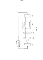
Атомные часы CPT-типа имеют лазерный элемент, ячейку, заключающую в себе щелочной металл, и светоприемный элемент для светоприемного лазерного света, пропущенного через ячейку, при этом лазерный свет модулируется и два перехода электрона в атоме щелочного металла одновременно достигаются посредством длин волн боковой полосы частот, возникающих на обеих сторонах несущей волны при конкретной длине волны, чтобы проводить его возбуждение. Энергия перехода для такого перехода является неизменной, и когда длина волны боковой полосы частот лазерного света совпадает с длиной волны, соответствующей энергии перехода, возникает явление повышения прозрачности, при котором понижается интенсивность поглощения света щелочного металла. Таким образом, такие атомные часы отличаются тем, что длина волны несущей волны регулируется с тем, чтобы понижать интенсивность поглощения света щелочного металла, и сигнал, детектируемый посредством светоприемного элемента, возвращается в модулятор, так что частота модуляции лазерного света из лазерного элемента регулируется посредством модулятора. Дополнительно, в таких атомных часах, лазерный свет, испускаемый из лазерного элемента, облучает ячейку, заключающую в себе щелочной металл, через коллиматор и волновую пластину λ/4.Atomic clocks of the CPT type have a laser element, a cell containing alkaline metal, and a light-receiving element for light-receiving laser light transmitted through the cell, the laser light being modulated and two electron transitions in the alkali metal atom simultaneously achieved by means of wavelengths of the side frequency band arising on both sides of the carrier wave at a specific wavelength in order to conduct its excitation. The transition energy for such a transition is unchanged, and when the wavelength of the side frequency band of the laser light coincides with the wavelength corresponding to the transition energy, a phenomenon of increasing transparency occurs, at which the light absorption intensity of the alkali metal decreases. Thus, such an atomic clock is characterized in that the wavelength of the carrier wave is adjusted so as to reduce the light absorption rate of the alkali metal, and the signal detected by the light receiving element is returned to the modulator, so that the modulation frequency of the laser light from the laser element is controlled by the modulator . Additionally, in such an atomic clock, laser light emitted from a laser element irradiates a cell containing an alkali metal through a collimator and a λ / 4 wave plate.
Для источника света для таких атомных часов очень компактного типа является подходящим компактный лазер поверхностного испускания с очень низким потреблением электроэнергии и высоким качеством длины волны, и желательно, чтобы точность длины волны несущей волны находилась в пределах +1 нм относительно конкретной длины волны (например, Proc. of SPIE, издание 6132 613208-1 (2006)).For a light source for such a very compact type atomic clock, a compact surface-emitting laser with very low power consumption and high wavelength quality is suitable, and it is desirable that the carrier wavelength accuracy is within +1 nm with respect to a specific wavelength (e.g., Proc . of SPIE, publication 6132 613208-1 (2006)).
В то же время, когда лазерный элемент поверхностного испускания используется для атомных часов, может быть необходимо обеспечить узкий интервал длин волн (5 нм) для каждого лазера поверхностного испускания. Следовательно, слой регулирования длины волны сформирован на области резонатора лазера поверхностного испускания, и соответственно, когда сформирован такой лазер поверхностного испускания с узким интервалом длин волн, может быть необходимо сформировать пленку таким образом, чтобы толщина каждой пленки в слое регулирования длины волны была очень тонкой. Однако, во время формирования полупроводникового слоя может быть затруднительно сформировать пленку таким образом, чтобы толщина каждой пленки для формирования слоя регулирования длины волны была чрезвычайно тонкой и однородной, вследствие дисперсии скорости роста, нерегулярности в распределении толщин пленки и т.д.At the same time, when a surface-emitting laser element is used for an atomic clock, it may be necessary to provide a narrow wavelength interval (5 nm) for each surface-emitting laser. Therefore, a wavelength adjustment layer is formed on the region of the surface emitting laser cavity, and accordingly, when such a surface emission laser is formed with a narrow wavelength interval, it may be necessary to form a film so that the thickness of each film in the wavelength adjustment layer is very thin. However, during the formation of the semiconductor layer, it may be difficult to form a film so that the thickness of each film for forming the wavelength adjustment layer is extremely thin and uniform, due to dispersion of the growth rate, irregularity in the distribution of film thicknesses, etc.
В частности, как указано в патенте (Япония) № 2751814, когда слой регулирования длины волны сформирован на области резонатора и когда интервал длины волны осцилляции должен составлять 5 нм или меньше, может быть необходимо, чтобы толщина пленки слоя регулирования длины волны составляла 1,2 нм или меньше, но для существующей технологии выращивания кристалла компаундного полупроводника может быть чрезвычайно трудно управлять настолько тонкой толщиной пленки. Таким образом, даже если толщина пленки немного изменена, длина волны осцилляции подвержена воздействию за счет этого.In particular, as indicated in Japanese Patent No. 2751814, when the wavelength adjustment layer is formed on the resonator region and when the oscillation wavelength interval is 5 nm or less, it may be necessary that the film thickness of the wavelength adjustment layer be 1.2 nm or less, but it can be extremely difficult to control such a thin film thickness for existing compound crystal semiconductor crystal growing technology. Thus, even if the film thickness is slightly changed, the wavelength of the oscillations is affected due to this.
СУЩНОСТЬ ИЗОБРЕТЕНИЯSUMMARY OF THE INVENTION
Согласно одному аспекту настоящего изобретения, может быть предусмотрен лазерный элемент поверхностного испускания, включающий в себя полупроводниковую подложку и множество лазеров поверхностного испускания, сконфигурированных с возможностью испускать свет со взаимно различными длинами волн, причем каждый лазер поверхностного испускания включает в себя нижний брэгговский отражатель, обеспеченный на полупроводниковой подложке, резонатор, обеспеченный на нижнем брэгговском отражателе, верхний брэгговский отражатель, обеспеченный на резонаторе, и слой регулирования длины волны, обеспеченный в верхнем брэгговском отражателе или нижнем брэгговском отражателе, причем слои регулирования длины волны, включенные в лазеры поверхностного испускания, имеют взаимно различные толщины, причем, по меньшей мере, один из слоев регулирования длины волны включает в себя слои регулирования, образованные из двух видов материалов, и при этом числа слоев регулирования, включенных в слои регулирования длины волны, являются взаимно различными.According to one aspect of the present invention, a surface emitting laser element may be provided, including a semiconductor substrate and a plurality of surface emitting lasers configured to emit light with mutually different wavelengths, each surface emitting laser including a lower Bragg reflector provided on a semiconductor substrate, a resonator provided on the lower Bragg reflector, an upper Bragg reflector provided on the resonator, and a wavelength adjustment layer provided in the upper Bragg reflector or lower Bragg reflector, wherein the wavelength adjustment layers included in surface emitting lasers have mutually different thicknesses, and at least one of the wavelength adjustment layers includes control layers formed from two types of materials, and the number of control layers included in the wavelength adjustment layers is mutually different.
Согласно другому аспекту настоящего изобретения, может быть обеспечен способ для изготовления лазерного элемента поверхностного испускания, включающего в себя множество лазеров поверхностного испускания, сконфигурированных с возможностью испускать свет со взаимно различными длинами волн, включающий в себя этапы формирования нижнего брэгговского отражателя на полупроводниковой подложке, формирования резонатора на нижнем брэгговском отражателе, формирования верхнего брэгговского отражателя на резонаторе, наслаивания слоев регулирования, образованных из двух видов материалов, в верхнем брэгговском отражателе или нижнем брэгговском отражателе, чтобы сформировать слой регулирования длины волны, удаления одного слоя регулирования в слое регулирования длины волны посредством использования первой текучей среды травления и удаления другого слоя регулирования в слое регулирования длины волны посредством использования второй текучей среды травления, отличающейся от первой текучей среды травления, так что слои регулирования длины волны, включенные в лазеры поверхностного испускания, имеют взаимно различные толщины, а также числа слоев регулирования, включенных в слои регулирования длины волны, являются взаимно различными.According to another aspect of the present invention, a method for manufacturing a surface emitting laser element including a plurality of surface emitting lasers configured to emit light with mutually different wavelengths, including the steps of forming a lower Bragg reflector on a semiconductor substrate, forming a resonator, can be provided according to another aspect of the present invention. on the lower Bragg reflector, the formation of the upper Bragg reflector on the resonator, layering formed from two kinds of materials in the upper Bragg reflector or the lower Bragg reflector to form a wavelength adjustment layer, removing one regulation layer in the wavelength adjustment layer by using the first etching fluid and removing another regulation layer in the wavelength adjustment layer by using a second etching fluid different from the first etching fluid, so that the wavelength control layers included in the surface lasers stnogo emission, have mutually different thicknesses, as well as regulation of layers included in the wavelength adjustment layers are mutually different.
Согласно другому аспекту настоящего изобретения, может быть обеспечен атомный осциллятор, включающий в себя лазерный элемент поверхностного испускания, как описано выше, ячейку с щелочным металлом, включающую в себя щелочной металл, который должен облучаться светом, испускаемым из лазерного элемента поверхностного испускания, фотодетектор, сконфигурированный с возможностью детектирования света, пропускаемого через ячейку с щелочным металлом, и блок управления, сконфигурированный с возможностью управления частотой осцилляции лазерного элемента поверхностного испускания на основе света, детектируемого посредством фотодетектора.According to another aspect of the present invention, an atomic oscillator may be provided including a surface emitting laser element as described above, an alkali metal cell including alkali metal to be irradiated with light emitted from the surface emitting laser element, a photodetector configured with the possibility of detecting the light transmitted through the cell with an alkali metal, and a control unit configured to control the oscillation frequency of the laser of a surface emitting element based on light detected by a photodetector.
КРАТКОЕ ОПИСАНИЕ ЧЕРТЕЖЕЙBRIEF DESCRIPTION OF THE DRAWINGS
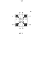
Фиг. 1 является видом сверху лазерного элемента поверхностного испускания в первом варианте осуществления.FIG. 1 is a plan view of a surface emitting laser element in a first embodiment.
Фиг. 2 является иллюстративной схемой лазерного элемента поверхностного испускания в первом варианте осуществления.FIG. 2 is an illustrative diagram of a surface emitting laser element in a first embodiment.
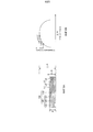
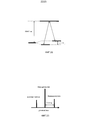
Фиг. 3 является структурной схемой слоя регулирования длины волны лазерного элемента поверхностного испускания в первом варианте осуществления.FIG. 3 is a block diagram of a wavelength adjustment layer of a surface emitting laser element in the first embodiment.
Фиг. 4A и фиг. 4B являются иллюстративными схемами (1) слоя регулирования длины волны лазерного элемента поверхностного испускания в первом варианте осуществления.FIG. 4A and FIG. 4B are illustrative diagrams (1) of a wavelength adjustment layer of a surface emitting laser element in a first embodiment.
Фиг. 5A и фиг. 5B являются иллюстративными схемами (2) слоя регулирования длины волны лазерного элемента поверхностного испускания в первом варианте осуществления.FIG. 5A and FIG. 5B are illustrative diagrams (2) of a wavelength adjustment layer of a surface emitting laser element in a first embodiment.
Фиг. 6A и фиг. 6B являются иллюстративными схемами (3) слоя регулирования длины волны лазерного элемента поверхностного испускания в первом варианте осуществления.FIG. 6A and FIG. 6B are illustrative diagrams (3) of a wavelength adjustment layer of a surface emitting laser element in a first embodiment.
Фиг. 7A и фиг. 7B являются иллюстративными схемами (4) слоя регулирования длины волны лазерного элемента поверхностного излучения в первом варианте осуществления.FIG. 7A and FIG. 7B are illustrative diagrams (4) of a wavelength adjustment layer of a surface radiation laser element in the first embodiment.
Фиг. 8 является иллюстративной схемой (5) слоя регулирования длины волны лазерного элемента поверхностного испускания в первом варианте осуществления.FIG. 8 is an illustrative diagram (5) of a wavelength adjustment layer of a surface emitting laser element in a first embodiment.
Фиг. 9 является иллюстративной схемой (6) слоя регулирования длины волны лазерного элемента поверхностного испускания в первом варианте осуществления.FIG. 9 is an illustrative diagram (6) of a wavelength adjustment layer of a surface emitting laser element in the first embodiment.
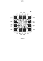
Фиг. 10 является видом сверху лазерного элемента поверхностного испускания во втором варианте осуществления.FIG. 10 is a plan view of a surface emitting laser element in a second embodiment.
Фиг. 11 является иллюстративной схемой лазерного элемента поверхностного испускания во втором варианте осуществления.FIG. 11 is an illustrative diagram of a surface emitting laser element in a second embodiment.
Фиг. 12A и фиг. 12B являются иллюстративными схемами (1) слоя регулирования длины волны лазерного элемента поверхностного испускания во втором варианте осуществления.FIG. 12A and FIG. 12B are illustrative diagrams (1) of a wavelength adjustment layer of a surface emitting laser element in a second embodiment.
Фиг. 13A и фиг. 13B являются иллюстративными схемами (2) слоя регулирования длины волны лазерного элемента поверхностного испускания во втором варианте осуществления.FIG. 13A and FIG. 13B are illustrative diagrams (2) of a wavelength adjustment layer of a surface emitting laser element in a second embodiment.
Фиг. 14 является видом сверху лазерного элемента поверхностного испускания в третьем варианте осуществления.FIG. 14 is a plan view of a surface emitting laser element in a third embodiment.
Фиг. 15A и фиг. 15B являются иллюстративными схемами лазерного элемента поверхностного испускания в третьем варианте осуществления.FIG. 15A and FIG. 15B are illustrative diagrams of a surface emitting laser element in a third embodiment.
Фиг. 16 является схемой корреляции между первым слоем регулирования длины волны и вторым слоем регулирования длины волны, а также длиной волны осцилляции.FIG. 16 is a correlation diagram between the first wavelength adjustment layer and the second wavelength adjustment layer as well as the oscillation wavelength.
Фиг. 17A и фиг. 17B являются иллюстративными схемами (1) первого слоя регулирования длины волны лазерного элемента поверхностного испускания в третьем варианте осуществления.FIG. 17A and FIG. 17B are illustrative diagrams (1) of a first wavelength control layer of a surface emitting laser element in a third embodiment.
Фиг. 18A и фиг. 18B являются иллюстративными схемами (2) первого слоя регулирования длины волны лазерного элемента поверхностного испускания в третьем варианте осуществления.FIG. 18A and FIG. 18B are illustrative diagrams (2) of a first wavelength control layer of a surface emitting laser element in a third embodiment.
Фиг. 19A и фиг. 19B являются иллюстративными схемами (3) первого слоя регулирования длины волны лазерного элемента поверхностного испускания в третьем варианте осуществления.FIG. 19A and FIG. 19B are illustrative diagrams (3) of a first wavelength control layer of a surface emitting laser element in a third embodiment.
Фиг. 20 является видом сверху лазерного элемента поверхностного испускания в четвертом варианте осуществления.FIG. 20 is a plan view of a surface emitting laser element in a fourth embodiment.
Фиг. 21 является структурной схемой атомного осциллятора в пятом варианте осуществления.FIG. 21 is a block diagram of an atomic oscillator in a fifth embodiment.
Фиг. 22 является иллюстративной схемой атомного энергетического уровня для иллюстрации CPT-типа.FIG. 22 is an illustrative atomic energy level diagram for illustrating a CPT type.
Фиг. 23 является иллюстративной схемой выходной длины волны во время модуляции лазера поверхностного испускания.FIG. 23 is an illustrative diagram of an output wavelength during modulation of a surface emitting laser.
Фиг. 24 является схемой корреляции между частотой модуляции и количеством пропускаемого света.FIG. 24 is a correlation diagram between the modulation frequency and the amount of transmitted light.
Вариант(ы) осуществления для реализации изобретенияOption (s) for implementing the invention
Ниже описывается вариант(ы) осуществления настоящего изобретения. Дополнительно, идентичные ссылки с номерами применяются к идентичным элементам и т.д., и их описание опускается.Embodiment (s) of the present invention are described below. Additionally, identical reference numbers apply to identical elements, etc., and their description is omitted.
ПЕРВЫЙ ВАРИАНТ ОСУЩЕСТВЛЕНИЯFIRST IMPLEMENTATION
КОНСТРУКЦИЯ ЛАЗЕРНОГО ЭЛЕМЕНТА ПОВЕРХНОСТНОГО ИСПУСКАНИЯSURFACE LASER LASER ELEMENT DESIGN
Ниже описывается лазерный элемент поверхностного испускания в первом варианте осуществления. Как проиллюстрировано на фиг. 1 и фиг. 2A, лазерный элемент 10 поверхностного испускания в настоящем варианте осуществления имеет множество лазеров поверхностного испускания и, в частности, имеет первый лазер 11 поверхностного испускания, второй лазер 12 поверхностного испускания, третий лазер 13 поверхностного испускания и четвертый лазер 14 поверхностного испускания. Дополнительно, фиг. 1 упрощена в целях пояснения настоящего варианта осуществления, при этом для удобства опущено изображение контактного слоя и т.д. Кроме того, фиг. 2 является схемой в поперечном сечении, обеспеченной посредством разреза вдоль штрихпунктирной линии 1A-1B на фиг. 1.The surface emitting laser element in the first embodiment is described below. As illustrated in FIG. 1 and FIG. 2A, the surface emitting
Лазерный элемент 10 поверхностного испускания в настоящем варианте осуществления сформирован на полупроводниковом кристалле в 300 квадратных мкм, при этом каждый из первого лазера 11 поверхностного испускания, второго лазера 12 поверхностного испускания, третьего лазера 13 поверхностного испускания и четвертого лазера 14 поверхностного испускания, сформированных на таком полупроводниковом кристалле, соединен с электродной контактной площадкой, обеспеченной соответственно для него. В частности, электродная контактная площадка 21 соединена с первым лазером 11 поверхностного испускания, а электродная контактная площадка 22 соединена со вторым лазером 12 поверхностного испускания, в то время как электродная контактная площадка 23 соединена с третьим лазером 13 поверхностного испускания, а электродная контактная площадка 24 соединена с четвертым лазером 14 поверхностного испускания.The surface emitting
Кроме того, первый лазер 11 поверхностного испускания, второй лазер 12 поверхностного испускания, третий лазер 13 поверхностного испускания и четвертый лазер 14 поверхностного испускания обеспечивают испускаемый свет со взаимно различными длинами волн. А именно, длина λ1 волны, испускаемая из первого лазера 11 поверхностного испускания, длина λ2 волны, испускаемая из второго лазера 12 поверхностного испускания, длина λ3 волны, испускаемая из третьего лазера 13 поверхностного испускания, и длина λ4 волны, испускаемая из четвертого лазера 14 поверхностного испускания, представляют собой взаимно различные длины волн.In addition, the first surface-emitting
Дополнительно, лазерный элемент поверхностного испускания в настоящем варианте осуществления должен получить лазер поверхностного испускания с длиной волны осцилляции в 894,6 нм, при этом четыре лазера поверхностного испускания сформированы на полупроводниковом кристалле (подложке) в 300 квадратных мкм. Поскольку может быть возможно сформировать множество лазеров поверхностного испускания в узкой области в лазерном элементе поверхностного испускания, существует малое изменение позиции точки испускания света, даже когда включается лазер поверхностного испускания для проведения испускания света. Следовательно, размер подложки представляет собой размер в 500×500 мкм или меньше, в силу чего регулирование оптической оси и т.д. может не являться необходимостью или быть чрезвычайно упрощенным.Additionally, the surface emitting laser element in the present embodiment is to receive a surface emitting laser with an oscillation wavelength of 894.6 nm, with four surface emitting lasers formed on a 300 square micron semiconductor crystal (substrate). Since it may be possible to form a plurality of surface emitting lasers in a narrow region in the surface emitting laser element, there is a small change in position of the light emitting point, even when the surface emitting laser is turned on to conduct light emitting. Therefore, the size of the substrate is a size of 500 × 500 μm or less, due to which the regulation of the optical axis, etc. may not be necessary or extremely simplified.
Для лазерного элемента поверхностного испускания в настоящем варианте осуществления полупроводниковые материалы с различными показателями преломления попеременно наслоены и сформированы на подложке 101, образованной из полупроводника и т.д.; чтобы сформировать нижний брэгговский отражатель 102, и нижний разделительный слой 103, активный слой 104 и верхний разделительный слой 105 сформированы на нижнем брэгговском отражателе 102. Первый верхний брэгговский отражатель 106, контактный слой 110, область 120 регулирования длины волны и второй верхний брэгговский отражатель 107 сформированы на верхнем разделительном слое 105. Кроме того, верхний электрод 111 сформирован на и соединен с контактным слоем 110, а нижний электрод 112 сформирован на задней поверхности подложки 101. Хотя слой 130 регулирования длины волны состоит из контактного слоя 110 и области 120 регулирования длины волны в настоящем варианте осуществления, слой 130 регулирования длины волны может состоять только из области 120 регулирования длины волны в случае, если контактный слой 110 не сформирован в прилегании к области 120 регулирования длины волны. Дополнительно, нижний брэгговский отражатель 102, нижний разделительный слой 103, активный слой 104, верхний разделительный слой 105, первый верхний брэгговский отражатель 106, контактный слой 110 и область 120 регулирования длины волны, которые представляют собой полупроводниковые слои, сформированные на подложке 101, сформированы посредством эпитаксиального выращивания полупроводниковых материалов. В частности, такие полупроводниковые слои сформированы посредством эпитаксиального выращивания в химическом осаждении паров металлоорганических соединений (MOCVD) или молекулярно-лучевой эпитаксии (MBE). Дополнительно, брэгговский отражатель, как описано в спецификации для настоящей заявки, может описываться как распределенный брэгговский отражатель (DBR).For the surface emitting laser element in the present embodiment, semiconductor materials with different refractive indices are alternately layered and formed on a
Кроме того, второй верхний брэгговский отражатель 107 сформирован на слое 130 регулирования длины волны для каждого лазера поверхностного испускания. Второй верхний брэгговский отражатель 107 является диэлектрической пленкой, образованной из оксида, нитрида, фторида и т.д. и сформированной посредством попеременного наслаивания и формирования пленки(ок) из материала с высоким показателем преломления и пленки(ок) из материала с низким показателем преломления. Дополнительно, верхний брэгговский отражатель состоит из первого верхнего брэгговского отражателя 106, слоя 130 регулирования длины волны и второго верхнего брэгговского отражателя 107 в настоящем варианте осуществления. Кроме того, слой 130 регулирования длины волны может быть сформирован в нижнем брэгговском отражателе 102.In addition, a second
В лазерном элементе поверхностного испускания в настоящем варианте осуществления, толщины областей 120 регулирования длины волны в слоях 130 регулирования длины волны в первом лазере 11 поверхностного испускания, втором лазере 12 поверхностного испускания, третьем лазере 13 поверхностного испускания и четвертом лазере 14 поверхностного испускания различаются. В частности, как проиллюстрировано на фиг. 3, область 120 регулирования длины волны сформирована на контактном слое 110, при этом область 120 регулирования длины волны состоит из первого слоя 121 регулирования, второго слоя 122 регулирования и третьего слоя 123 регулирования. В настоящем варианте осуществления, первый слой 121 регулирования и третий слой 123 регулирования образованы из GaInP, в то время как второй слой 122 регулирования образован из GaAsP. Дополнительно, материалы для образования первого слоя 121 регулирования, второго слоя 122 регулирования и третьего слоя 123 регулирования могут быть противоположными по свойствам.In the surface emitting laser element in the present embodiment, the thicknesses of the
Таким образом, толщины областей 120 регулирования длины волны в первом лазере 11 поверхностного испускания, втором лазере 12 поверхностного испускания, третьем лазере 13 поверхностного испускания и четвертом лазере 14 поверхностного испускания различаются в лазерном элементе поверхностного испускания в настоящем варианте осуществления.Thus, the thicknesses of the
В частности, первый слой 121 регулирования, второй слой 122 регулирования и третий слой 123 регулирования сформированы в области 120 регулирования длины волны в первом лазере 11 поверхностного испускания, в котором испускается свет с длиной волны λ1, которая соответствует толщине слоя 130 регулирования длины волны, который является суммой такой области 120 регулирования длины волны и контактного слоя 110.In particular, the
Далее, первый слой 121 регулирования и второй слой 122 регулирования сформированы в области 120 регулирования длины волны во втором лазере 12 поверхностного испускания, в котором испускается свет с длиной волны λ2, которая соответствует толщине слоя 130 регулирования длины волны, который является суммой такой области 120 регулирования длины волны и контактного слоя 110.Further, the
Далее, первый слой 121 регулирования сформирован в области 120 регулирования длины волны в третьем лазере 13 поверхностного испускания, в котором испускается свет с длиной волны λ3, которая соответствует толщине слоя 130 регулирования длины волны, который является суммой такой области 120 регулирования длины волны и контактного слоя 110.Further, a
При этом, область 120 регулирования длины волны не сформирована в четвертом лазере 14 поверхностного испускания, и следовательно, испускается свет с длиной волны λ4, которая соответствует толщине слоя 130 регулирования длины волны, которая равна толщине контактного слоя 110.Moreover, the
Таким образом, может быть возможно изменять толщины слоев 130 регулирования длины волны в первом лазере 11 поверхностного испускания, втором лазере 12 поверхностного испускания, третьем лазере 13 поверхностного испускания и четвертом лазере 14 поверхностного испускания мало-помалу и может быть возможно испускать свет с каждой длиной волны, соответствующей толщине, по меньшей мере, одного или каждого из слоев 130 регулирования длины волны.Thus, it may be possible to change the thicknesses of the wavelength adjustment layers 130 in the first
СПОСОБ ДЛЯ ИЗГОТОВЛЕНИЯ ЛАЗЕРНОГО ЭЛЕМЕНТА ПОВЕРХНОСТНОГО ИСПУСКАНИЯMETHOD FOR PRODUCING SURFACE LASER LASER ELEMENT
В настоящем варианте осуществления, подложка n-GaAs используется для подложки 101. Кроме того, нижний брэгговский отражатель 102 сформирован посредством наслаивания 35,5 пар из слоя n-Al0,1Ga0,9As с высоким показателем преломления и слоя n-Al0,9Ga0,1As с низким показателем преломления таким образом, что толщина оптической пленки каждого слоя составляет λ/4.In the present embodiment, the n-GaAs substrate is used for the
Активный слой 104, состоящий из слоя квантовых ям GaInAs/барьерного слоя GaInPAs, сформирован на нижнем брэгговском отражателе 102 посредством нижнего разделительного слоя 103, образованного из Al0,2Ga0,8As. Верхний разделительный слой 105, образованный из Al0,2Ga0,8As и первого верхнего брэгговского отражателя 106, сформирован на активном слое 104. Дополнительно, область резонатора, обеспеченная с оптической толщиной в одну длину волны, состоит из нижнего разделительного слоя 103, активного слоя 104 и верхнего разделительного слоя 105.An
Первый верхний брэгговский отражатель 106 сформирован посредством наслаивания 6 пар из слоя n-Al0,1Ga0,9As с высоким показателем преломления и слоя n-Al0,9Ga0,1As с низким показателем преломления таким образом, что толщина оптической пленки каждого слоя составляет λ/4. Один из слоев с низким показателем преломления первого верхнего брэгговского отражателя 106 состоит из слоя 108 сужения электрического тока, образованного из AlAs, в котором периферийная часть слоя 108 сужения электрического тока избирательно окисляется с возможностью формирования области 108a избирательного окисления, а неокисленная область 108b сужения электрического тока сформирована в его центральной части.The first
Контактный слой 110, образованный из p-GaAs, и область 120 регулирования длины волны, состоящая из первого слоя 121 регулирования, второго слоя 122 регулирования и третьего слоя 123 регулирования, сформированы на первом верхнем брэгговском отражателе 106. Дополнительно, часть слоев в области 120 регулирования длины волны удалена, чтобы соответствовать длине волны, испускаемой из каждого лазера поверхностного испускания, как описано выше.A
Каждый лазер поверхностного испускания в лазерном элементе поверхностного испускания в настоящем варианте осуществления имеет мезаструктуру, в котором такая мезаструктура сформирована посредством удаления полупроводникового слоя между лазерами поверхностного испускания, которые должны сформироваться, вследствие травления. После того, как сформирована мезаструктура, проводится термическая обработка в водяном паре, чтобы окислить слой 108 сужения электрического тока от периферии мезаструктуры, в силу чего формируются область 108a избирательного окисления (окисленная область) в периферийной части и неокисленная область 108b сужения электрического тока в центральной части. Иными словами, слой 108 сужения электрического тока состоит из окисленной области 108a избирательного окисления и неокисленной области 108b сужения электрического тока, чтобы обеспечить структуру сужения электрического тока. Дополнительно, очертание при просмотре сверху мезаструктуры может быть сформировано как круглое очертание либо может быть сформировано как эллиптическое очертание, квадратное очертание или прямоугольное очертание.Each surface emitting laser in the surface emitting laser element in the present embodiment has a mesastructure in which such a mesastructure is formed by removing a semiconductor layer between the surface emitting lasers that must be formed due to etching. After the mesastructure is formed, heat treatment is performed in water vapor to oxidize the electric
Кроме того, второй верхний брэгговский отражатель 107 сформирован на слое 130 регулирования длины волны, в котором удаление, соответствующее каждому лазеру поверхностного испускания, проводится посредством травления. Второй верхний брэгговский отражатель 107 сформирован посредством наслаивания 8,5 пар из слоя TiO2 с высоким показателем преломления и слоя SiO2 с низким показателем преломления таким образом, что толщина оптической пленки каждого слоя составляет λ/4. Дополнительно, может быть необходимо только то, чтобы второй верхний брэгговский отражатель 107 был образован из диэлектрического материала(ов) и сформирован посредством наслаивания материала с высоким показателем преломления и материала с низким показателем преломления, при этом, в частности, может быть возможно, обеспечить такой материал, как оксид, нитрид или фторид. Для материала с высоким показателем преломления может быть возможно обеспечить Ta2O5, HfO2 и т.д., а также TiO2. Кроме того, для материала с низким показателем преломления может быть возможно обеспечить MgF2 и т.д., а также SiO2. Для способа для формирования слоя TiO2 с высоким показателем преломления и слоя SiO2 с низким показателем преломления во втором верхнем брэгговском отражателе 107 формирование проводится посредством напыления или вакуумного осаждения и т.д. Кроме того, защитная пленка 140, образованная из SiN, сформирована всеохватывающим образом, и полимерная пленка 141, образованная из полимерного материала, такого как полиимид, сформирована между мезаструктурами соответствующих лазеров поверхностного испускания.In addition, a second
Далее, сформирован верхний электрод 111, который представляет собой электрод p-стороны. Каждый такой верхний электрод 111 сформирован, чтобы соответствовать каждому лазеру поверхностного испускания, при этом каждый верхний электрод 111 соединен с каждой из электродных контактных площадок 21-24. Кроме того, нижний электрод 112, который представляет собой электрод n-стороны, сформирован на задней поверхности подложки 101.Further, the
Далее подробно описывается способ для формирования слоя 130 регулирования длины волны в лазерном элементе поверхностного испускания в настоящем варианте осуществления.The following describes in detail a method for forming a
Во-первых, нижний брэгговский отражатель 102, нижний разделительный слой 103, активный слой 104, верхний разделительный слой 105, первый верхний брэгговский отражатель 106, контактный слой 110 и область 120 регулирования длины волны, которые образованы из полупроводниковых материалов, сформированы на подложке 101 посредством эпитаксиального выращивания согласно MOCVD или MBE. Дополнительно, слой 130 регулирования длины волны состоит из контактного слоя 110 и области 120 регулирования длины волны, при этом область 120 регулирования длины волны формируется посредством наслаивания первого слоя 121 регулирования, второго слоя 122 регулирования и третьего слоя 123 регулирования. В данном документе, как упомянуто выше, первый слой 121 регулирования и третий слой 123 регулирования образованы из GaInP, в то время как второй слой 122 регулирования образован из GaAsP.Firstly, the
Затем, контур сопротивления сформирован на области, на которой сформирован первый лазер 11 поверхностного испускания. В частности, контур сопротивления сформирован посредством применения вещества с фотосопротивлением на третьем слое 123 регулирования в области 120 регулирования длины волны и проведения его светового экспонирования и проявки посредством устройства светового экспонирования.Then, a resistance loop is formed on the region in which the first
Затем, третий слой 123 регулирования на области, на которой не сформирован контур сопротивления, удаляется посредством влажного травления. В частности, влажное травление проводится посредством смешанной текучей среды из соляной кислоты и воды, поскольку третий слой 123 регулирования образован из GaInP. В силу этого, только третий слой 123 регулирования на области, на которой не сформирован контур сопротивления, удаляется, чтобы экспонировать поверхность второго слоя 122 регулирования. Дополнительно, может быть возможно для такой смешанной текучей среды проводить травление GaInP, образующего третий слой 123 регулирования, но может быть практически невозможно проводить травление GaAsP, образующего второй слой 122 регулирования. Такая смешанная текучая среда также может описываться как первая текучая среда травления. Впоследствии, контур сопротивления удаляется посредством органического растворителя и т.д.Then, the
Затем, контур сопротивления сформирован на области, на которой сформирован первый лазер 11 поверхностного испускания и второй лазер 12 поверхностного испускания. В частности, контур сопротивления сформирован посредством применения вещества с фотосопротивлением на третьем слое 123 регулирования и втором слое 122 регулирования на области 120 регулирования длины волны и проведения его светового экспонирования и проявки посредством устройства оптического экспонирования.Then, a resistance loop is formed on a region in which the first
Затем, второй слой 122 регулирования на области, на которой не сформирован контур сопротивления, удаляется посредством влажного травления. В частности, влажное травление проводится посредством смешанной текучей среды из серной кислоты, перекиси водорода и воды, поскольку второй слой 122 регулирования изготавливается из GaAsP. В силу этого, только второй слой 122 регулирования на области, на которой не сформирован контур сопротивления, удаляется, чтобы экспонировать поверхность первого слоя 121 регулирования. Дополнительно, может быть возможно для такой смешанной текучей среды проводить травление GaAsP, образующего второй слой 122 регулирования, но может быть практически невозможно проводить травление GaInP, образующего первый слой 121 регулирования. Такая смешанная текучая среда может описываться как вторая текучая среда травления. Впоследствии, контур сопротивления удаляется посредством органического растворителя и т.д.Then, the
Затем, контур сопротивления сформирован на области, на которой сформированы первый лазер 11 поверхностного испускания, второй лазер 12 поверхностного испускания и третий лазер 13 поверхностного испускания. В частности, контур сопротивления сформирован посредством применения вещества с фотосопротивлением на первом слое 121 регулирования, втором слое 122 регулирования и третьем слое 123 регулирования в области 120 регулирования длины волны и проведения его светового экспонирования и проявки посредством устройства светового экспонирования.Then, a resistance loop is formed on a region in which the first
Затем, первый слой 121 регулирования на области, на которой не сформирован контур сопротивления, удаляется посредством влажного травления. В частности, первый слой 121 регулирования на области, на которой не сформирован контур сопротивления, удаляется посредством первой текучей среды травления. В силу этого, только первый слой 121 регулирования на области, на которой не сформирован контур сопротивления, удаляется, чтобы экспонировать поверхность контактного слоя 110. Впоследствии, контур сопротивления удаляется посредством органического растворителя и т.д.Then, the
Далее, сформирован второй верхний брэгговский отражатель 107. В частности, формирование проводится посредством попеременного наслаивания диэлектрической пленки, образованной из материала с высоким показателем преломления, и диэлектрической пленки, образованной из материала с низким показателем преломления, которые состоят из оксида, нитрида, фторида и т.д., каждая из которых имеет предварительно определенную толщину пленки вследствие напыления и т.д. Дополнительно, также может быть возможно сформировать второй верхний брэгговский отражатель 107 посредством наслаивания и формирования полупроводниковых материалов с различными показателями преломления.Next, a second
В силу этого, может быть возможно сформировать слой 130 регулирования длины волны и второй верхний брэгговский отражатель 107 в лазерном элементе поверхностного испускания в настоящем варианте осуществления.Therefore, it may be possible to form a
В настоящем варианте осуществления Al не включен ни в один из первого слоя 121 регулирования, второго слоя 122 регулирования и третьего слоя 123 регулирования, составляющих область 120 регулирования длины волны в слое 130 регулирования длины волны, и следовательно, окисление и т.д. практически не вызывается после травления, в силу чего может быть возможно поддерживать чистое состояние поверхности после травления. Иными словами, Al может чрезвычайно просто подвергаться коррозии, и следовательно, когда один из первого слоя 121 регулирования, второго слоя 122 регулирования и третьего слоя 123 регулирования формируется посредством материала, включающего в себя Al, состояние поверхности после проведения влажного травления и т.д. может быть плохим, при этом даже если второй верхний брэгговский отражатель 107 сформирован на ней, может возникать ее отслаивание, либо ее толщина может быть неоднородной. Тем не менее, область 120 регулирования длины волны в лазерном элементе поверхностного испускания в настоящем варианте осуществления сформирована посредством материала, не включающего в себя Al, и следовательно, коррозия Al и т.д. может не вызываться, и такая проблема может не возникать.In the present embodiment, Al is not included in any of the
Кроме того, область 120 регулирования длины волны в слое 130 регулирования длины волны в настоящем варианте осуществления образована посредством чередования GaAsP и GaInP, и при проведении влажного травления травление проводится посредством использования двух видов текучих сред травления, при этом, взаимно, может быть возможно проводить травление одного из них и может быть невозможно проводить травление другого из них. Травление проводится посредством использования двух таких видов текучих сред травления, в силу чего поверхность после травления может быть плоской, и может быть возможно проводить формирование с предварительно определенной толщиной без излишнего травления. В силу этого, может быть возможно получить лазерный элемент поверхностного испускания с устойчивой характеристикой.In addition, the
Дополнительно, хотя в описании для настоящего варианта осуществления описан случай комбинации GaAsP и GaInP, может быть обеспечена комбинация с другим материалом, не включающим в себя Al, который дополнительно обеспечен для другой текучей среды травления и представляет собой полупроводниковый материал с энергией запрещенной зоны, превышающей длину волны осцилляции. Для 894,6 нм, что представляет собой длину волны осцилляции в настоящем варианте осуществления, предусмотрена, например, GaInAsP/GaInP, GaAs/GaInP, GaAs/GaInAsP, GaAsP/GaInAsP и т.д. в качестве комбинации таких полупроводниковых материалов. Кроме того, N или Sb может добавляться в них, к примеру, GaAsN/GaInP, GaInNAs/GaInP, GaAsSb/GaInP и т.д.Additionally, although the case for the combination of GaAsP and GaInP is described in the description for the present embodiment, a combination with another material not including Al can be provided, which is further provided for another etching fluid and is a semiconductor material with a band gap energy exceeding the length oscillation waves. For 894.6 nm, which is the wavelength of the oscillations in the present embodiment, for example, GaInAsP / GaInP, GaAs / GaInP, GaAs / GaInAsP, GaAsP / GaInAsP, etc. are provided. as a combination of such semiconductor materials. In addition, N or Sb can be added to them, for example, GaAsN / GaInP, GaInNAs / GaInP, GaAsSb / GaInP, etc.
Как описано выше, может быть возможно сформировать множество лазеров поверхностного испускания для испускания света с различными длинами волн на одной подложке 101 в лазерном элементе поверхностного испускания в настоящем варианте осуществления. В силу этого, даже если изменение толщины пленки полупроводникового слоя и т.д. вызывается при изготовлении лазерного элемента поверхностного испускания, одно испускание света с длиной волны, ближайшей к желаемой длине волны, выбирается среди первого лазера 11 поверхностного испускания - четвертого лазера 14 поверхностного испускания, в силу чего может быть возможно легко получить полупроводниковый лазер с желаемой длиной волны. В силу этого, может быть возможно изготовить лазерный элемент поверхностного испускания, имеющий лазер поверхностного испускания, испускающий свет с предварительно определенной длиной волны, при низких затратах.As described above, it may be possible to form a plurality of surface emitting lasers for emitting light with different wavelengths on one
Дополнительно, когда контактный слой 110 сформирован в области 120 регулирования длины волны, количество электрического тока, способного протекать в каждом лазере поверхностного испускания и т.д., изменяется в зависимости от толщины области 120 регулирования длины волны, и электрическая характеристика и характеристика испускания света каждого лазера поверхностного испускания также могут значительно различаться. Кроме того, когда электрический ток протекает в области 120 регулирования длины волны, электрическое сопротивление может быть увеличено посредством несплошности полосы на границе раздела каждого слоя. Тем не менее, контактный слой 110 сформирован под областью 120 регулирования длины волны в лазерном элементе поверхностного испускания в настоящем варианте осуществления, в силу чего электрический ток, инжектированный в лазер поверхностного испускания, не может пройти через область 120 регулирования длины волны и сопротивление и т.д. не может быть изменено в зависимости от толщины области 120 регулирования длины волны.Further, when the
Далее описывается преимущество первого верхнего брэгговского отражателя 106, сформированного между слоем 130 регулирования длины волны и областью резонатора. Например, когда слой регулирования длины волны сформирован в области резонатора, имеющей оптическую длину в одну длину волны, и когда четыре длины волн обеспечены с центральной длиной волны в 895 нм и интервалом длин волн в 1 нм, один слой, составляющий слой регулирования длины волны, обеспечен с 1,3 нм, при этом может быть чрезвычайно трудно провести однородное формирование на поверхности пластины с помощью современной технологии выращивания кристаллов. Следовательно, первый верхний брэгговский отражатель 106, который является частью верхнего брэгговского отражателя, сформирован между областью резонатора и слоем 130 регулирования длины волны в настоящем варианте осуществления. В частности, первый верхний брэгговский отражатель 106 сформирован посредством наслаивания 6 пар из слоя n-Al0,1Ga0,9As с высоким показателем преломления и слоя n-Al0,9Ga0,1As с низким показателем преломления таким образом, что толщина оптической пленки каждого слоя составляет λ/4. Кроме того, контактный слой 110 сформирован на первом верхнем брэгговском отражателе 106, а область 120 регулирования длины волны сформирована на контактном слое 110. Первый слой 121 регулирования, второй слой 122 регулирования и третий слой 123 регулирования, составляющие область 120 регулирования длины волны, сформированы таким образом, что толщины пленок GaInP/GaAsP/GaInP составляют 16 нм/16 нм/16 нм, соответственно, при этом может быть возможно проводить существенно однородное изготовление согласно современной технологии выращивания кристаллов. Следовательно, может быть возможно уменьшить отклонение интервала длин волн среди лазеров поверхностного испускания.The following describes the advantage of the first
Кроме того, одновременно также может быть возможно уменьшить электрическое сопротивление посредством формирования такой структуры. Иными словами, второй верхний брэгговский отражатель 107, представляющий собой диэлектрик, сформирован поверх слоя 130 регулирования длины волны, а верхний электрод 111 сформирован в его окрестности, при этом когда слой регулирования длины волны обеспечен в области резонатора, может быть необходимо обеспечить слой AlAs, который должен быть избирательно окислен в позиции около контактного слоя с точки зрения структуры слоя, и канал электрического тока может быть узким для того, чтобы увеличить электрическое сопротивление. Здесь, первый верхний брэгговский отражатель 106 сформирован между слоем 130 регулирования длины волны (в котором контактный слой 110 сформирован под областью 120 регулирования длины волны) и областью резонатора в настоящем варианте осуществления, в силу чего может быть возможно продлить канал электрического тока и может быть возможно уменьшить электрическое сопротивление.In addition, at the same time, it may also be possible to reduce the electrical resistance by forming such a structure. In other words, a second
Дополнительно, может быть возможно дополнительно увеличить толщину пленки каждого слоя в области 120 регулирования длины волны в слое 130 регулирования длины волны посредством второго верхнего брэгговского отражателя 107, представляющего собой семь или более пар, за счет чего можно упростить однородное изготовление, а также можно уменьшить электрическое сопротивление. Тем не менее, если число пар во втором верхнем брэгговском отражателе 107 увеличивается, оптическая толщина слоя 130 регулирования длины волны может превышать λ/4 и полная отражательная способность верхнего отражателя может деградировать. Таким образом, оптимальное число пар может присутствовать для второго верхнего брэгговского отражателя 107, так что может быть возможно, что оптическая толщина слоя 130 регулирования длины волны составляет около λ/4.Additionally, it may be possible to further increase the film thickness of each layer in the
Далее описывается толщина слоя 130 регулирования длины волны. Когда оптическая толщина P слоя 130 регулирования длины волны составляет λ/4≤P<λ/2, как проиллюстрировано на фиг. 4A, может быть возможно то, что отражательные способности верхних брэгговских отражателей в первом лазере 11 поверхностного испускания, втором лазере 12 поверхностного испускания, третьем лазере 13 поверхностного испускания и четвертом лазере 14 поверхностного испускания, являются, в общем случае, постоянными, как проиллюстрировано на фиг. 4B. Дополнительно, L1 является поверхностью слоя 130 регулирования длины волны в первом лазере 11 поверхностного испускания, а L2 является поверхностью слоя 130 регулирования длины волны во втором лазере 12 поверхностного испускания, в то время как L3 является поверхностью слоя 130 регулирования длины волны в третьем лазере 13 поверхностного испускания, а L4 указывает поверхность слоя 130 регулирования длины волны в четвертом лазере 14 поверхностного испускания.The following describes the thickness of the
С другой стороны, когда оптическая толщина P слоя 130 регулирования длины волны составляет λ/2<P, как проиллюстрировано на фиг. 5A, отражательные способности верхних брэгговских отражателей в первом лазере 11 поверхностного испускания, втором лазере 12 поверхностного испускания, третьем лазере 13 поверхностного испускания и четвертом лазере 14 поверхностного испускания могут значительно различаться между собой, как проиллюстрировано на фиг. 5B.On the other hand, when the optical thickness P of the
Кроме того, когда оптическая толщина P слоя 130 регулирования длины волны составляет P<λ/4, как проиллюстрировано на фиг. 6A, отражательные способности верхних брэгговских отражателей в первом лазере 11 поверхностного испускания, втором лазере 12 поверхностного испускания, третьем лазере 13 поверхностного испускания и четвертом лазере 14 поверхностного испускания могут значительно различаться между собой, как проиллюстрировано на фиг. 6B.Furthermore, when the optical thickness P of the
Как описано выше, предпочтительно, когда оптическая толщина P слоя 130 регулирования длины волны составляет λ/4≤P<λ/2, и если такой подход обобщить, оптическая толщина предпочтительно составляет (2N-1)λ/4≤P<Nλ/2. Дополнительно, N является положительным целым числом, и если учитывается применение влияния поглощения света, чтобы вызвать отрицательный эффект, такой как увеличение порогового электрического тока, предпочтительно, когда N является малым.As described above, it is preferable that the optical thickness P of the
Кроме того, когда толщина области 120 регулирования длины волны является малой, и сумма оптических толщин области 120 регулирования длины волны и контактного слоя 110 меньше λ/4, область 131 регулирования фазы может быть обеспечена для слоя 130 регулирования длины волны, как проиллюстрировано на фиг. 7A. В силу этого, может быть возможно то, что оптическая толщина P слоя 130 регулирования длины волны составляет λ/4≤P<λ/2, и в общем, (2N-1)λ/4≤P<2Nλ/4, и как проиллюстрировано на фиг. 7B, может быть возможно то, что отражательные способности верхних брэгговских отражателей в первом лазере 11 поверхностного испускания, втором лазере 12 поверхностного испускания, третьем лазере 13 поверхностного испускания и четвертом лазере 14 поверхностного испускания, являются, в общем, постоянными. Дополнительно, в таком случае, слой 130 регулирования длины волны состоит из контактного слоя 110, области 120 регулирования длины волны и области 131 регулирования фазы. Кроме того, область 131 регулирования фазы изготавливается из AlGaAs, при этом область 131 регулирования фазы может формироваться под контактным слоем 110, как проиллюстрировано на фиг. 7A, или область 131 регулирования фазы может формироваться между контактным слоем 110 и областью 120 регулирования длины волны, как проиллюстрировано на фиг. 8. Кроме того, область регулирования фазы 131a может состоять из многослойной пленки, в которой GaAsP и GaInP попеременно наслоены, как проиллюстрировано на фиг. 9.Further, when the thickness of the
Кроме того, лазерный элемент поверхностного испускания в настоящем варианте осуществления имеет структуру, в которой несколько пленок сформированы в области 120 регулирования длины волны, при этом предпочтительно формировать слой 130 регулирования длины волны таким образом, что когда число слоев сформированной пленки(ок) (слоя(ев) регулирования) составляет M (при этом M является положительным целым числом), позиция, в которой толщина оптической пленки элемента составляет λ/4, представляет собой (M+1)/2-ю пленку (слой регулирования) в направлении сверху в случае, если M является нечетным числом, или M/2-ю или (M/2)+1-ю пленку (слой регулирования) в направлении сверху в случае, если M является четным числом.In addition, the surface emitting laser element in the present embodiment has a structure in which several films are formed in the
ВТОРОЙ ВАРИАНТ ОСУЩЕСТВЛЕНИЯSECOND EMBODIMENT
Далее описывается лазерный элемент поверхностного испускания во втором варианте осуществления. Дополнительно, лазерный элемент поверхностного испускания в настоящем варианте осуществления представляет собой лазер поверхностного испускания для длины волны в 894,6 нм и со структурой, в которой область регулирования длины волны обеспечена на нижнем брэгговском отражателе. Как проиллюстрировано на фиг. 10 и фиг. 11, лазерный элемент 150 поверхностного испускания в настоящем варианте осуществления имеет множество лазеров поверхностного испускания и, в частности, имеет первый лазер 151 поверхностного испускания, второй лазер 152 поверхностного испускания, третий лазер 153 поверхностного испускания и четвертый лазер 154 поверхностного испускания. Дополнительно, фиг. 10 упрощена в целях пояснения настоящего варианта осуществления, при этом для удобства опущено изображение контактного слоя и т.д. Кроме того, фиг. 11 является схемой в поперечном сечении, предоставленной посредством разреза вдоль штрихпунктирной линии 10A-10B на фиг. 10.The following describes the surface emitting laser element in the second embodiment. Additionally, the surface emitting laser element in the present embodiment is a surface emitting laser for a wavelength of 894.6 nm and with a structure in which a wavelength adjustment region is provided on the lower Bragg reflector. As illustrated in FIG. 10 and FIG. 11, the surface emitting
Лазерный элемент 150 поверхностного испускания в настоящем варианте осуществления сформирован на полупроводниковом кристалле в 300 квадратных мкм, при этом каждый из первого лазера 151 поверхностного испускания, второго лазера 152 поверхностного испускания, третьего лазера 153 поверхностного испускания и четвертого лазера 154 поверхностного испускания, сформированных на таком полупроводниковом кристалле, соединен с электродной контактной площадкой, обеспеченной для него. В частности, электродная контактная площадка 161 соединена с первым лазером 151 поверхностного испускания, а электродная контактная площадка 162 соединена со вторым лазером 152 поверхностного испускания, в то время как электродная контактная площадка 163 соединена с третьим лазером 153 поверхностного испускания, а электродная контактная площадка 164 соединена с четвертым лазером 154 поверхностного испускания.The surface emitting
Кроме того, первый лазер 151 поверхностного испускания, второй лазер 152 поверхностного испускания, третий лазер 153 поверхностного испускания и четвертый лазер 154 поверхностного испускания обеспечивают испускаемый свет со взаимно различными длинами волн. А именно, длина λ1 волны, испускаемая из первого лазера 151 поверхностного испускания, длина λ2 волны, испускаемая из второго лазера 152 поверхностного испускания, длина λ3 волны, испускаемая из третьего лазера 153 поверхностного испускания, и длина λ4 волны, испускаемая из четвертого лазера 154 поверхностного испускания, представляют собой взаимно различные длины волн.In addition, the first surface-emitting
Дополнительно, лазерный элемент поверхностного испускания в настоящем варианте осуществления должен получить лазер поверхностного испускания с длиной волны осцилляции 894,6 нм, при этом четыре лазера поверхностного испускания сформированы на полупроводниковом кристалле (подложке) в 300 квадратных мкм. Поскольку может быть возможно сформировать множество лазеров поверхностного испускания в узкой области в лазерном элементе поверхностного испускания, имеется несущественное изменение позиции точки светового испускания, даже когда включается лазер поверхностного испускания, который должен проводить световое испускание.Additionally, the surface emitting laser element in the present embodiment is to receive a surface emitting laser with an oscillation wavelength of 894.6 nm, with four surface emitting lasers formed on a 300 square micron semiconductor crystal (substrate). Since it may be possible to form a plurality of surface emitting lasers in a narrow region in the surface emitting laser element, there is an insignificant change in the position of the light emitting point, even when the surface emitting laser that is to conduct light emitting is turned on.
Для лазерного элемента поверхностного испускания в настоящем варианте осуществления, полупроводниковые материалы с различными показателями преломления попеременно наслоены и сформированы на подложке 101, образованной из полупроводника и т.д., с тем чтобы сформировать первый нижний брэгговский отражатель 172, и слой 173 регулирования фазы, область 180 регулирования длины волны, второй нижний брэгговский отражатель 174, нижний разделительный слой 103, активный слой 104 и верхний разделительный слой 105 сформированы на первом нижнем брэгговском отражателе 172. Верхний брэгговский отражатель 176 и контактный слой 177 сформированы на верхнем разделительном слое 105. Кроме того, верхний электрод 178 сформирован и соединен с контактным слоем 177, и нижний электрод 112 сформирован на задней поверхности подложки 101. Дополнительно, слой 190 регулирования длины волны состоит из области 180 регулирования длины волны и слоя 173 регулирования фазы в настоящем варианте осуществления, в то время как нижний брэгговский отражатель 170 состоит из первого нижнего брэгговского отражателя 172, области 173 регулирования фазы, области 180 регулирования длины волны и второго нижнего брэгговского отражателя 174.For the surface emitting laser element in the present embodiment, semiconductor materials with different refractive indices are alternately layered and formed on a
Кроме того, первый нижний брэгговский отражатель 172, область 173 регулирования фазы, область 180 регулирования длины волны, второй нижний брэгговский отражатель 174, нижний разделительный слой 103, активный слой 104, верхний разделительный слой 105, верхний брэгговский отражатель 176 и контактный слой 177, которые представляют собой полупроводниковые слои, сформированные на подложке 101, сформированы посредством эпитаксиального выращивания полупроводниковых материалов. В частности, такие полупроводниковые слои сформированы посредством эпитаксиального выращивания согласно MOCVD или MBE.In addition, the first
В лазерном элементе поверхностного испускания в настоящем варианте осуществления толщины соответствующих областей 180 регулирования длины волны в первом лазере 151 поверхностного испускания, втором лазере 152 поверхностного испускания, третьем лазере 153 поверхностного испускания и четвертом лазере 154 поверхностного испускания различаются между собой. В частности, область 180 регулирования длины волны состоит из первого слоя 181 регулирования, второго слоя 182 регулирования и третьего слоя 183 регулирования. В настоящем варианте осуществления, первый слой 181 регулирования и третий слой 183 регулирования образованы из GaInP, в то время как второй слой 182 регулирования образован из GaAsP. Дополнительно, материалы для образования первого слоя 181 регулирования, второго слоя 182 регулирования и третьего слоя 183 регулирования могут быть противоположны по свойствам.In the surface emitting laser element in the present embodiment, the thicknesses of the respective
Таким образом, толщины областей 180 регулирования длины волны, т.е. толщины слоев 190 регулирования длины волны в первом лазере 151 поверхностного испускания, втором лазере 152 поверхностного испускания, третьем лазере 153 поверхностного испускания и четвертом лазере поверхностного испускания 154 различаются в лазерном элементе поверхностного испускания в настоящем варианте осуществления.Thus, the thicknesses of the
В частности, первый слой 181 регулирования, второй слой 182 регулирования и третий слой 183 регулирования сформированы на области 180 регулирования длины волны в первом лазере 151 поверхностного испускания, при этом испускается свет с длиной волны λ1, которая соответствует толщине слоя 190 регулирования длины волны, который включает в себя такую область 180 регулирования длины волны.In particular, the
Кроме того, первый слой 181 регулирования и второй слой 182 регулирования сформированы в области 180 регулирования длины волны во втором лазере 152 поверхностного испускания, в котором испускается свет с длиной волны λ2, которая соответствует толщине слоя 190 регулирования длины волны, который включает в себя такую область 180 регулирования длины волны.In addition, the
Кроме того, первый слой 181 регулирования сформирован в области 180 регулирования длины волны в третьем лазере 153 поверхностного испускания, в котором испускается свет с длиной волны λ3, которая соответствует толщине слоя 190 регулирования длины волны, который включает в себя такую область 180 регулирования длины волны.In addition, a
Кроме того, область 180 регулирования длины волны не сформирована в четвертом лазере 154 поверхностного испускания, и следовательно, испускается свет с длиной волны λ4, которая соответствует толщине слоя 190 регулирования длины волны в случае, если область 180 регулирования длины волны не сформирована.In addition, the
Таким образом, может быть возможно изменять толщины областей 180 регулирования длины волны в первом лазере 151 поверхностного испускания, втором лазере 152 поверхностного испускания, третьем лазере 153 поверхностного испускания и четвертом лазере 154 поверхностного испускания мало помалу и может быть возможно испускать свет с каждой длиной волны, соответствующей толщине по меньшей мере одной или каждой из областей 180 регулирования длины волны.Thus, it may be possible to change the thicknesses of the
В настоящем варианте осуществления, подложка n-GaAs используется для подложки 101. Кроме того, нижний брэгговский отражатель 170 сформирован посредством наслаивания 35,5 пар из слоя n-Al0,1Ga0,9As с высоким показателем преломления и слоя n-Al0,9Ga0,1As с низким показателем преломления таким образом, что толщина оптической пленки каждого слоя составляет λ/4.In the present embodiment, the n-GaAs substrate is used for the
Как описано выше, нижний брэгговский отражатель 170 состоит из первого нижнего брэгговского отражательного зеркала 172, области 173 регулирования фазы, области 180 регулирования длины волны и второго нижнего брэгговского отражателя 174 на подложке 101. Следовательно, область 173 регулирования фазы и область 180 регулирования длины волны сформированы внутри нижнего брэгговского отражателя 170. Дополнительно, в настоящем варианте осуществления, формирование проведено таким образом, что сумма толщины оптической пленки области 173 регулирования фазы и половины толщины оптической пленки области 180 регулирования длины волны, т.е. толщины оптической пленки снизу области 173 регулирования фазы до центральной части области 180 регулирования длины волны, составляет λ/4, как проиллюстрировано на фиг. 12.As described above, the
Активный слой 104, состоящий из слоя на основе квантовых ям GaInAs/барьерного слоя GaInPAs, сформирован на нижнем брэгговском отражателе 170 посредством нижнего разделительного слоя 103, образованного из Al0,2Ga0,8As. Верхний разделительный слой 105, образованный из Al0,2Ga0,8As, сформирован на активном слое 104. Дополнительно, область резонатора, обеспеченный с оптической толщиной в одну длину волны, состоит из нижнего разделительного слоя 103, активного слоя 104 и верхнего разделительного слоя 105.An
Верхний брэгговский отражатель 176 сформирован посредством наслаивания 24 пар из слоя n-Al0,1Ga0,9As с высоким показателем преломления и слоя n-Al0,9Ga0,1As с низким показателем преломления таким образом, что толщина оптической пленки каждого слоя составляет λ/4. Один из слоев с низким показателем преломления верхнего брэгговского отражателя 176 состоит из слоя 108 сужения электрического тока, образованного из AlAs, при этом периферийная часть слоя 108 сужения электрического тока избирательно окислена чтобы сформировать область 108a избирательного окисления, а неокисленная область 108b сужения электрического тока сформирована в его центральной части. Кроме того, контактный слой 177, образованный из p-GaAs, сформирован на верхнем брэгговском отражателе 176.The
Когда сумма значения толщины оптической пленки области 173 регулирования фазы и значения половины толщины оптической пленки области 180 регулирования длины волны составляет приблизительно λ/4, как проиллюстрировано на фиг. 12A, может быть возможно, что отражательные способности нижних брэгговских отражателей в первом лазере 151 поверхностного испускания, втором лазере 152 поверхностного испускания, третьем лазере 153 поверхностного испускания и четвертом лазере 154 поверхностного испускания являются, в общем, постоянными, как проиллюстрировано на фиг. 12B. Дополнительно, L1 является поверхностью слоя 190 регулирования длины волны в первом лазере 151 поверхностного испускания, и L2 является поверхностью слоя 190 регулирования длины волны во втором лазере 152 поверхностного испускания, в то время как L3 является поверхностью слоя 190 регулирования длины волны в третьем лазере 153 поверхностного испускания, и L4 указывает поверхность слоя 190 регулирования длины волны в четвертом лазере 154 поверхностного испускания.When the sum of the thickness values of the optical film of the
Каждый лазер поверхностного испускания в лазерном элементе поверхностного испускания в настоящем варианте осуществления имеет мезаструктуру, при этом такая мезаструктура сформирована посредством удаления полупроводникового слоя между лазерами поверхностного испускания, которые должны быть сформированы, вследствие сухого травления и т.д. После того как сформирована мезаструктура, проводится термическая обработка в водяном паре, чтобы окислить слой 108 сужения электрического тока от периферии мезаструктуры, в силу чего сформированы область 108a избирательного окисления (окисленная область) на периферийной части и неокисленная область 108b сужения электрического тока в центральной части. Иными словами, слой 108 сужения электрического тока состоит из окисленной области 108a избирательного окисления и неокисленной области 108b сужения электрического тока, чтобы обеспечить структуру сужения электрического тока. В частности, AlAs, образующий слой 108 сужения электрического тока, подвергается термической обработке в водяном паре, чтобы быть окисленным и сформировать AlxOy, при этом таким образом сформированный AlxOy образует область 108a избирательного окисления. В данном варианте осуществления, область 108b сужения электрического тока сформирована из неокисленного AlAs в слое 108 сужения электрического тока. Дополнительно, очертание при просмотре сверху мезаструктуры может быть сформировано как круглое очертание либо может быть сформировано как эллиптическое очертание, квадратное очертание или прямоугольное очертание.Each surface emitting laser in the surface emitting laser element in the present embodiment has a mesastructure, wherein such a mesastructure is formed by removing a semiconductor layer between the surface emitting lasers that must be formed due to dry etching, etc. After the mesastructure is formed, heat treatment is performed in water vapor to oxidize the electric
Кроме того, защитная пленка 140, образованная из SiN, сформирована целостным образом, и полимерная 141 сформирована между мезаструктурами соответствующих лазеров поверхностного испускания посредством внедрения полимерного материала, такого как полиимид. Далее, сформирован верхний электрод 178, который представляет собой электрод p-стороны. Каждый такой верхний электрод 178 сформирован таким образом, что он соответствует каждому лазеру поверхностного испускания, при этом каждый верхний электрод 178 соединяется с каждой из электродных контактных площадок 161-164.In addition, the
В частности, сформирована защитная пленка 140, образованная из SiN, и полимерный слой 141 сформирован посредством внедрения и планаризации полимерного материала, такого как полиимид, между мезаструктурами соответствующих лазеров поверхностного испускания. Впоследствии, защитная пленка 140 и полимерный слой 141 на контактном слое 177 удаляются, чтобы экспонировать контактный слой 177, и верхний электрод 178 сформирован на контактном слое 177. Дополнительно, нижний электрод 112, который представляет собой электрод n-стороны, сформирован на задней поверхности подложки 101.In particular, a
Лазерный элемент поверхностного испускания в настоящем варианте осуществления испускает лазерный свет на противоположной стороне стороны подложки 101. Дополнительно, может быть возможно, что защитная пленка 140, образованная из SiN, защищает боковую поверхность и нижнюю поверхность слоя, включающего в себя Al, который появляется вследствие вытравливания мезаструктур и легко корродирует вследствие его диэлектрика в настоящем варианте осуществления, и следовательно, может быть возможно улучшить надежность.The surface emitting laser element in the present embodiment emits laser light on the opposite side of the side of the
Далее описывается преимущество второго нижнего брэгговского отражателя 174, сформированного между областью 180 регулирования длины волны и резонатором. Когда область регулирования длины волны сформирована в резонаторе, имеющем оптическую длину в одну длину волны, и когда четыре длины волны обеспечены с центральной длиной волны в 895 нм и интервалом длин волн в 1 нм, один слой из слоев регулирования, составляющих слой регулирования длины волны, обеспечен приблизительно с 1 нм, при этом может быть чрезвычайно трудно проводить однородное формирование на поверхности пластины с помощью современной технологии выращивания кристаллов.The following describes the advantage of the second
Следовательно, второй нижний брэгговский отражатель 174, который является частью нижнего брэгговского отражателя 170, сформирован между резонатором и областью 180 регулирования длины волны в настоящем варианте осуществления. В частности, второй нижний брэгговский отражатель 174 сформирован посредством наслаивания 10 пар из слоя n-Al0,1Ga0,9As с высоким показателем преломления и слоя n-Al0,9Ga0,1As с низким показателем преломления таким образом, что толщина оптической пленки каждого слоя составляет λ/4. В силу этого, может быть возможно, что толщины пленок GaInP/GaAsP/GaInP в первом слое 181 регулирования, втором слое 182 регулирования и третьем слое 183 регулирования, из которых состоит область 180 регулирования длины волны, составляют 16 нм/16 нм/16 нм, соответственно, и может быть возможно проводить достаточно равномерное изготовление согласно современной технологии выращивания кристаллов, в силу чего может быть возможно уменьшать отклонение интервала длин волн аналогично первому варианту осуществления.Therefore, the second
Дополнительно, когда второй нижний брэгговский отражатель 174 состоит из одиннадцати или более пар, может быть возможно, что толщина пленки каждого слоя в области 180 регулирования длины волны, является еще большей, и следовательно, может быть возможно дополнительно улучшить однородность. Тем не менее, если число пары(пар) во втором нижнем брэгговском отражателе 174 увеличивается, как проиллюстрировано на фиг. 13A и фиг. 13B, толщина оптической пленки области 180 регулирования длины волны может намного превышать λ/4 (толщину оптической пленки брэгговского отражателя), и следовательно, может ухудшиться в целом отражательная способность нижнего брэгговского отражателя 170, что не является предпочтительным. Таким образом, оптимальное число пар может присутствовать для второго нижнего брэгговского отражателя, так что оптическая толщина области 180 регулирования длины волны должна составить около λ/4.Further, when the second
С другой стороны, когда сумма значения толщины оптической пленки области 173 регулирования фазы и значения половины толщины оптической пленки области 180 регулирования длины волны составляет λ/4 или больше, как проиллюстрировано на фиг. 13A, отражательная способность нижнего брэгговского отражателя в каждом из первого лазера 151 поверхностного испускания, второго лазера 152 поверхностного испускания, третьего лазера 153 поверхностного испускания и четвертого лазера 154 поверхностного испускания может быть большой, как проиллюстрировано на фиг. 13B. Тем не менее, в настоящем варианте осуществления может быть возможно повысить однородность отражательной способности каждого нижнего брэгговского отражателя, как проиллюстрировано на фиг. 12B.On the other hand, when the sum of the thickness value of the optical film of the
Далее подробно описывается способ для формирования области 180 регулирования длины волны в лазерном элементе поверхностного испускания в настоящем варианте осуществления.The method for forming the
Во-первых, первый нижний брэгговский отражатель 172, область 173 регулирования фазы и область 180 регулирования длины волны, которые образованы из полупроводниковых материалов, сформированы на подложке 101 посредством эпитаксиального выращивания согласно MOCVD или MBE. Как описано выше, слой 190 регулирования длины волны состоит из области 173 регулирования фазы и области 180 регулирования длины волны, в котором область 180 регулирования длины волны сформирована посредством наслаивания первого слоя 181 регулирования, второго слоя 182 регулирования и третьего слоя 183 регулирования. Дополнительно, первый слой 181 регулирования и третий слой 183 регулирования образованы из GaInP, в то время как второй слой 182 регулирования образован из GaAsP.First, the first
Затем, контур сопротивления сформирован на области, на которой сформирован первый лазер 151 поверхностного испускания. В частности, контур сопротивления сформирован посредством применения вещества с фотосопротивлением на третьем слое 183 регулирования в области 180 регулирования длины волны и проведения его светового экспонирования и проявки посредством устройства светового экспонирования.Then, a resistance loop is formed on a region in which the first
Затем, третий слой 183 регулирования на области, на которой не сформирован контур сопротивления, удаляется посредством влажного травления. В частности, влажное травление проводится посредством смешанной текучей среды из соляной кислоты и воды, поскольку третий слой 183 регулирования образован из GaInP. В силу этого, только третий слой 183 регулирования на области, на которой не сформирован контур сопротивления, удаляется, чтобы экспонировать поверхность второго слоя 182 регулирования. Дополнительно, может быть возможно, что такая смешанная текучая среда проводит травление GaInP, образующего третий слой 183 регулирования, но может быть практически невозможно, что она проводит травление GaAsP, образующего второй слой 182 регулирования. Такая смешанная текучая среда также может описываться как первая текучая среда травления. Далее, контур сопротивления удаляется посредством органического растворителя и т.д.Then, the
Затем, контур сопротивления сформирован на области, на которой сформированы первый лазер 151 поверхностного испускания и второй лазер 152 поверхностного испускания. В частности, контур сопротивления сформирован посредством применения вещества с фотосопротивлением на третьем слое 183 регулирования и втором слое 182 регулирования на области 180 регулирования длины волны и проведения его светового экспонирования и проявки посредством устройства светового экспонирования.Then, a resistance loop is formed on a region in which the first
Затем, второй слой 182 регулирования на области, на которой не сформирован контур сопротивления, удаляется посредством влажного травления. В частности, влажное травление проводится посредством смешанной текучей среды из серной кислоты, перекиси водорода и воды, поскольку второй слой 182 регулирования образован из GaAsP. В силу этого, только второй слой 182 регулирования на области, на которой не сформирован контур сопротивления, удаляется, чтобы экспонировать поверхность первого слоя 181 регулирования. Дополнительно, может быть возможно, что такая смешанная текучая среда проводит травление GaAsP, образующего второй слой 182 регулирования, но может быть практически невозможно, что она проводит травление GaInP, образующего первый слой 181 регулирования. Такая смешанная текучая среда может описываться как вторая текучая среда травления. Впоследствии, контур сопротивления удаляется посредством органического растворителя и т.д.Then, the
Затем, контур сопротивления сформирован на области, на которой сформированы первый лазер 151 поверхностного спускания, второй лазер 152 поверхностного испускания и третий лазер 153 поверхностного испускания. В частности, контур сопротивления сформирован посредством применения вещества с фотосопротивлением на первом слое 181 регулирования, втором слое 182 регулирования и третьем слое 183 регулирования на области 180 регулирования длины волны и проведения его светового экспонирования и проявки посредством устройства светового экспонирования.Then, a resistance loop is formed on a region in which the first
Затем, первый слой 181 регулирования на области, на которой не сформирован контур сопротивления, удаляется посредством влажного травления. В частности, первый слой 181 регулирования на области, на которой не сформирован контур сопротивления, удаляется посредством первой текучей среды травления. В силу этого, только первый слой 181 регулирования на области, на которой не сформирован контур сопротивления, удаляется, чтобы экспонировать поверхность слоя 173 регулирования фазы. Далее, контур сопротивления удаляется посредством органического растворителя и т.д.Then, the
Затем, сформирован второй нижний брэгговский отражатель 174. В силу этого, может быть возможно сформировать нижний брэгговский отражатель 170, включающий в себя область 180 регулирования длины волны, в лазерном элементе поверхностного испускания в настоящем варианте осуществления.Then, the second
В настоящем варианте осуществления, Al не включен ни в один из первого слоя 181 регулирования, второго слоя 182 регулирования и третьего слоя 183 регулирования, из которых состоит область 180 регулирования длины волны в слое 190 регулирования длины волны, и следовательно, окисление и т.д. практически не вызывается после травления, в силу чего может быть возможно поддержать чистое состояние поверхности после травления. Иными словами, Al может чрезвычайно легко корродировать, и следовательно, когда один из первого слоя 181 регулирования, второго слоя 182 регулирования и третьего слоя 183 регулирования сформирован посредством материала, включающего в себя Al, состояние поверхности после проведения влажного травления и т.д. может быть плохим, при этом даже если второй нижний брэгговский отражатель 174 сформирован на ней, может вызываться ее отслаивание, либо ее толщина может быть неоднородной. Однако область 180 регулирования длины волны в лазерном элементе поверхностного испускания в настоящем варианте осуществления сформирована посредством материала, не включающего в себя Al, и следовательно, коррозия Al и т.д. не может вызываться, и такая проблема может не возникать.In the present embodiment, Al is not included in any of the
Кроме того, область 180 регулирования длины волны в слое 190 регулирования длины волны в настоящем варианте осуществления образована из чередования GaAsP и GaInP, и когда проводится влажное травление, травление проводится посредством использования двух видов текучих сред травления, при этом взаимно может быть возможно проводить травление одного из них и может быть возможным не проводить травление другого. Поскольку травление проводится посредством использования двух таких видов текучих сред травления, поверхность после травления может быть плоской, и может быть возможно проводить формирование с предварительно определенной толщиной без излишнего травления. В силу этого, может быть возможно получить лазерный элемент поверхностного испускания с устойчивой характеристикой.In addition, the
Дополнительно, хотя в описании (описаниях) для настоящего варианта осуществления описан случай комбинации GaAsP и GaInP, может быть обеспечена комбинация с другим материалом, не включающим в себя Al, который дополнительно обеспечен для другой текучей среды травления и представляет собой полупроводниковый материал с энергией запрещенной зоны, большей длины волны осцилляции. Для 894,6 нм, что представляет собой длину волны осцилляции в настоящем варианте осуществления, обеспечена, например, GaInAsP/GaInP, GaAs/GaInP, GaAs/GaInAsP, GaAsP/GaInAsP и т.д. в качестве комбинации таких полупроводниковых материалов. Кроме того, N или Sb могут быть добавлены в них, к примеру, GaAsN/GaInP, GaInNAs/GaInP, GaAsSb/GaInP и т.д.Additionally, although a case of a combination of GaAsP and GaInP is described in the description (s) for this embodiment, a combination with another material not including Al can be provided, which is further provided for another etching fluid and is a band gap energy semiconductor material greater wavelength of oscillations. For 894.6 nm, which is the wavelength of the oscillations in the present embodiment, provided, for example, GaInAsP / GaInP, GaAs / GaInP, GaAs / GaInAsP, GaAsP / GaInAsP, etc. as a combination of such semiconductor materials. In addition, N or Sb can be added to them, for example, GaAsN / GaInP, GaInNAs / GaInP, GaAsSb / GaInP, etc.
Как описано выше, может быть возможно сформировать множество лазеров поверхностного испускания для испускания света с различными длинами волн на одной подложке 101 в лазерном элементе поверхностного испускания в настоящем варианте осуществления. В силу этого, даже если вариация толщины пленки полупроводникового слоя и т.д. вызывается при изготовлении лазерного элемента поверхностного испускания, одно испускание света с длиной волны, ближайшей к желаемой длине волны, выбирается среди первого лазера 151 поверхностного испускания - четвертого лазера 154 поверхностного испускания, в силу чего может быть возможно легко получить полупроводниковый лазер с требуемой длиной волны. В силу этого, может быть возможно изготовить лазерный элемент поверхностного испускания, имеющий лазер поверхностного испускания, испускающий свет с предварительно определенной длиной волны, при низких затратах.As described above, it may be possible to form a plurality of surface emitting lasers for emitting light with different wavelengths on one
Дополнительно, содержание (содержания) помимо описанного выше, является/являются аналогичным(и) первому варианту осуществления.Additionally, the content (s) other than those described above are / are similar to (and) the first embodiment.
ТРЕТИЙ ВАРИАНТ ОСУЩЕСТВЛЕНИЯTHIRD EMBODIMENT
Далее поясняется третий вариант осуществления. Лазер поверхностного испускания в настоящем варианте осуществления представляет собой лазер поверхностного испускания с 12 каналами для длины волны в 780 нм и описывается на основе фиг. 14 и фиг. 15. Дополнительно, фиг. 14 является видом сверху лазера поверхностного испускания в настоящем варианте осуществления, в то время как фиг. 15A является схемой в поперечном сечении, предоставленной посредством разреза вдоль штрихпунктирной линии 14A-14B на фиг. 14, а фиг. 15B является схемой в поперечном сечении, предоставленной посредством разреза вдоль штрихпунктирной линии 14C-14D на фиг. 14.Next, a third embodiment is explained. The surface emitting laser in the present embodiment is a 12-channel surface emitting laser for a wavelength of 780 nm and is described based on FIG. 14 and FIG. 15. Additionally, FIG. 14 is a plan view of a surface emitting laser in the present embodiment, while FIG. 15A is a cross-sectional diagram provided by section along the dot-
Лазерный элемент 200 поверхностного испускания в настоящем варианте осуществления сформирован на полупроводниковом кристалле в 300 квадратных мкм, при этом каждый из первого лазера 201 поверхностного испускания, второго лазера 202 поверхностного испускания, третьего лазера 203 поверхностного испускания, четвертого лазера 204 поверхностного испускания, пятого лазера 205 поверхностного испускания, шестого лазера 206 поверхностного испускания, седьмого лазера 207 поверхностного испускания, восьмого лазера 208 поверхностного испускания, девятого лазера 209 поверхностного испускания, десятого лазера 210 поверхностного испускания, одиннадцатого лазера 211 поверхностного испускания и двенадцатого лазера 212 поверхностного испускания, сформированных на таком полупроводниковом кристалле, соединен с электродной контактной площадкой, предоставленной для него.The surface emitting
В частности, электродная контактная площадка 221 соединена с первым лазером 201 поверхностного испускания, электродная контактная площадка 222 соединена со вторым лазером 202 поверхностного испускания, электродная контактная площадка 223 соединена с третьим лазером 203 поверхностного испускания, электродная контактная площадка 224 соединена с четвертым лазером 204 поверхностного испускания, электродная контактная площадка 225 соединена с пятым лазером 205 поверхностного испускания, электродная контактная площадка 226 соединена с шестым лазером 206 поверхностного испускания, электродная контактная площадка 227 соединена с седьмым лазером 207 поверхностного испускания, электродная контактная площадка 228 соединена с восьмым лазером 208 поверхностного испускания, электродная контактная площадка 229 соединена с девятым лазером 209 поверхностного испускания, электродная контактная площадка 230 соединена с десятым лазером 210 поверхностного испускания, электродная контактная площадка 231 соединена с одиннадцатым лазером 211 поверхностного испускания, а электродная контактная площадка 232 соединена с двенадцатым лазером 212 поверхностного испускания.In particular, the
Кроме того, первый лазер 201 поверхностного испускания, второй лазер 202 поверхностного испускания, третий лазер 203 поверхностного испускания, четвертый лазер 204 поверхностного испускания, пятый лазер 205 поверхностного испускания, шестой лазер 206 поверхностного испускания, седьмой лазер 207 поверхностного испускания, восьмой лазер 208 поверхностного испускания, девятый лазер 209 поверхностного испускания, десятый лазер 210 поверхностного испускания, одиннадцатый лазер 211 поверхностного испускания и двенадцатый лазер 212 поверхностного испускания обеспечивают испускаемый свет со взаимно различными длинами волн. А именно, длина λ1 волны, испускаемая из первого лазера поверхностного испускания 201, длина λ2 волны, испускаемая из второго лазера 202 поверхностного испускания, длина λ3 волны, испускаемая из третьего лазера 203 поверхностного испускания, длина λ4 волны, испускаемая из четвертого лазера 204 поверхностного испускания, длина λ5 волны, испускаемая из пятого лазера 205 поверхностного испускания, длина λ6 волны, испускаемая из шестого лазера 206 поверхностного испускания, длина λ7 волны, испускаемая из седьмого лазера 207 поверхностного испускания, длина λ8 волны, испускаемая из восьмого лазера 208 поверхностного испускания, длина λ9 волны, испускаемая из девятого лазера 209 поверхностного испускания, длина λ10 волны, испускаемая из десятого лазера 210 поверхностного испускания, длина λ11 волны, испускаемая из одиннадцатого лазера 211 поверхностного испускания, и длина λ12 волны, испускаемая из двенадцатого лазера 212 поверхностного испускания, представляют собой взаимно различные длины волн.In addition, the first
Для лазерного элемента поверхностного испускания в настоящем варианте осуществления, нижний брэгговский отражатель 102, нижний разделительный слой 103, активный слой 104, верхний разделительный слой 105, первый верхний брэгговский отражатель 106 сформированы на подложке 101, образованной из полупроводника и т.д., и первый слой 250 регулирования длины волны, второй верхний брэгговский отражатель 271, второй слой 260 регулирования длины волны, третий верхний брэгговский отражатель 272, контактный слой 240 и верхний электрод 111 сформированы на первом верхнем брэгговском отражателе 106. Кроме того, контактный слой 240 соединен с верхним электродом 111, и нижний электрод 112 сформирован на задней поверхности подложки 101. Дополнительно, в настоящем варианте осуществления, нижний брэгговский отражатель 102, нижний разделительный слой 103, активный слой 104, верхний разделительный слой 105, первый верхний брэгговский отражатель 106, первый слой 250 регулирования длины волны, второй верхний брэгговский отражатель 271, второй слой 260 регулирования длины волны и контактный слой 240 третьего верхнего брэгговского отражателя 272, которые представляют собой полупроводниковые слои, сформированные на подложке 101, сформированы посредством эпитаксиального выращивания полупроводниковых материалов. В частности, такие полупроводниковые слои формируются посредством эпитаксиального выращивания согласно MOCVD или MBE. Дополнительно, в настоящем варианте осуществления, верхний брэгговский отражатель состоит из первого верхнего брэгговского отражателя 106, первого слоя 250 регулирования длины волны, второго верхнего брэгговского отражателя 271, второго слоя 260 регулирования длины волны и третьего верхнего брэгговского отражателя 272. Кроме того, первый слой 250 регулирования длины волны и второй слой 260 регулирования длины волны могут быть сформированы в нижнем брэгговском отражателе 102.For the surface emitting laser element in the present embodiment, the
В настоящем варианте осуществления, подложка n-GaAs используется для подложки 101. Кроме того, нижний брэгговский отражатель 102 сформирован посредством наслаивания 35,5 пар из слоя n-Al0,1Ga0,9As с высоким показателем преломления и слоя n-Al0,9Ga0,1As с низким показателем преломления таким способом, что толщина оптической пленки каждого слоя составляет λ/4.In the present embodiment, the n-GaAs substrate is used for the
Активный слой 104, состоящий из слоя на основе квантовых ям GaInAs/барьерного слоя GaInPAs, сформирован на нижнем брэгговском отражателе 102 посредством нижнего разделительного слоя 103, образованного из Al0,2Ga0,8As. Верхний разделительный слой 105, образованный из Al0,2Ga0,8As, и первый верхний брэгговский отражатель 106 сформированы на активном слое 104. Дополнительно, область резонатора, обеспеченная с оптической толщиной в одну длину волны, состоит из нижнего разделительного слоя 103, активного слоя 104 и верхнего разделительного слоя 105.An
Первый верхний брэгговский отражатель 106 сформирован посредством наслаивания 3,5 пар из слоя n-Al0,1Ga0,9As с высоким показателем преломления и слоя n-Al0,9Ga0,1As с низким показателем преломления таким образом, что толщина оптической пленки каждого слоя составляет λ/4. Дополнительно, один из слоев с низким показателем преломления первого верхнего брэгговского отражателя 106 состоит из слоя 108 сужения электрического тока, образованного из AlAs, который не проиллюстрирован на фиг. 15A и фиг. 15B.The first
Первый слой 250 регулирования длины волны сформирован на первом верхнем брэгговском отражателе 106. Первый слой 250 регулирования длины волны сформирован посредством наслаивания области 254 регулирования фазы, образованной из p-Al0,1Ga0,9As, первого слоя 251 регулирования, образованного из GaInP, второго слоя 252 регулирования, образованного из GaAsP, и третьего слоя 253 регулирования, образованного из GaInP.A first
Второй верхний брэгговский отражатель 271 сформирован на первом слое 250 регулирования длины волны. Второй верхний брэгговский отражатель 271 сформирован посредством наслаивания 4,5 пар из слоя n-Al0,1Ga0,9As с высоким показателем преломления и слоя n-Al0,9Ga0,1As с низким показателем преломления таким образом, что толщина оптической пленки каждого слоя составляет λ/4.A second
Второй слой 260 регулирования длины волны сформирован на втором верхнем брэгговском отражателе 271. Второй слой 260 регулирования длины волны сформирован посредством наслаивания области 263 регулирования фазы, образованной из p-Al0,1Ga0,9As, четвертого слоя 261 регулирования, образованного из GaInP, и пятого слоя 262 регулирования, образованного из GaAsP.A second
Третий верхний брэгговский отражатель 272 сформирован на втором слое 260 регулирования длины волны. Третий верхний брэгговский отражатель 272 сформирован посредством наслаивания 17 пар из слоя n-Al0,1Ga0,9As с высоким показателем преломления и слоя n-Al0,9Ga0,1As с низким показателем преломления таким образом, что толщина оптической пленки каждого слоя составляет λ/4.A third
Контактный слой 240, образованный из p-GaAs, сформирован на третьем верхнем брэгговском отражателе 272, в то время как верхний электрод 111 сформирован на контактном слое 240, и нижний электрод 112 сформирован на задней стороне подложки 101.The
В настоящем варианте осуществления, каждый лазер поверхностного испускания сформирован таким образом, что первый слой 250 регулирования длины волны и второй слой 260 регулирования длины волны имеют различные толщины для каждого соответствующего канала. Дополнительно, может быть возможно сформировать и первый слой 250 регулирования длины волны и второй слой 260 регулирования с различными толщинами посредством способа, аналогичного первому варианту осуществления. В частности, может быть возможно провести формирование посредством проведения литографии и избирательного травления таким образом, что числа слоя(ев) в слоях регулирования длины волны различаются. Например, когда GaAsP (аналогично для случая GaAs) подвергается травлению, может быть возможно использовать смешанную текучую среду из серной кислоты, перекиси водорода и воды, а когда GaInP подвергается травлению, может быть возможно использовать смешанную текучую среду из соляной кислоты и воды. После того как проведено избирательное травление первого слоя 250 регулирования длины волны, второй верхний брэгговский отражатель 271 и второй слой 260 регулирования длины волны сформированы посредством выращивания кристаллов, далее проводится избирательное травление второго слоя 260 регулирования длины волны, и третий верхний BDR 272 и контактный слой 240 формируются посредством выращивания кристаллов. Дополнительно, травление мезаструктуры, необходимой для формирования каждого лазера поверхностного испускания, проводится посредством сухого травления. Дополнительно, верхний электрод 111, который представляет собой электрод p-стороны каждого лазера поверхностного испускания, сформирован на контактном слое 240, и нижний электрод 112, который представляет собой общий электрод n-стороны, сформирован на задней поверхности подложки 101, как проиллюстрировано на фиг. 15A и фиг. 15B. Лазерный элемент поверхностного испускания в настоящем варианте осуществления испускает лазерный свет на противоположной стороне подложки 101.In the present embodiment, each surface emitting laser is formed such that the first
В патенте (Япония) № 2751814 слой регулирования длины волны сформирован в области резонатора, имеющий оптическую толщину в одну длину волны. Например, в таком случае, если центральная длина волны составляет 780 нм и интервал длин волн составляет 3 нм, один слой, из которого состоит слой регулирования длины волны, обеспечен с 0,9 нм. Такая толщина соответствует приблизительно трем атомным слоям, и может быть затруднительно провести однородное формирование на поверхности пластины с помощью современной технологии выращивания кристаллов. Кроме того, если обеспечивается область резонатора с оптической длиной длины волны X (X=2, 3, …), толщина пленки может увеличиваться так, что она составит 0,9xX нм для одного слоя, из которого состоит слой регулирования длины волны, но в таком случае длина волны релаксационной осцилляции может ухудшиться в X-1/2 раз, так что может возникнуть такой отрицательный эффект, что операция для высокоскоростной модуляции может быть затруднительной и т.д.In the patent (Japan) No. 2751814, a wavelength adjustment layer is formed in the cavity region having an optical thickness of one wavelength. For example, in such a case, if the central wavelength is 780 nm and the wavelength interval is 3 nm, one layer of which the wavelength adjustment layer consists is provided with 0.9 nm. Such a thickness corresponds to approximately three atomic layers, and it may be difficult to conduct uniform formation on the wafer surface using modern crystal growing technology. In addition, if a resonator region with an optical wavelength of X (X = 2, 3, ...) is provided, the film thickness may increase so that it is 0.9xX nm for one layer of which the wavelength control layer consists, but in In this case, the wavelength of the relaxation oscillation can be degraded by X -1/2 times, so that a negative effect can occur that the operation for high-speed modulation can be difficult, etc.
С другой стороны, в лазерном элементе поверхностного испускания в настоящем варианте осуществления первый верхний брэгговский отражатель 106 сформирован между областью резонатора и слоем 250 регулирования длины волны, как проиллюстрировано на фиг. 15A и фиг. 15B. В частности, первый верхний брэгговский отражатель 106 сформирован посредством попеременного наслаивания 4,5 пар из слоя p-Al0,1Ga0,9As с высоким показателем преломления и слоя n-Al0,9Ga0,1As с низким показателем преломления между первым слоем 250 регулирования длины волны и областью резонатора. В таком случае, даже когда интервал длины волны осцилляции между различными светоизлучающими элементами составляет 3 нм, толщины пленки GaInP/GaAsP/GaInP, из которых состоит первый слой 250 регулирования длины волны, составляют 11,6 нм/11,6 нм/11,6 нм, соответственно, при этом может быть возможно провести достаточно однородное изготовление согласно современной технологии выращивания кристаллов. Следовательно, может быть возможно уменьшить отклонение интервала длин волн между лазерами поверхностного испускания.On the other hand, in the surface emitting laser element in the present embodiment, a first
Кроме того, второй верхний брэгговский отражатель 271 и второй слой 260 регулирования длины волны дополнительно сформированы на первом слое 250 регулирования длины волны. В силу этого, может быть возможно сформировать первый слой 250 регулирования длины волны более однородно, в то время как интервал длины волны осцилляции является суженным. Фиг. 16 иллюстрирует взаимосвязь между толщинами пленки первого слоя 250 регулирования длины волны и второго слоя 260 регулирования длины волны (как указано посредством толщин оптической пленки, при этом λ/4 упоминается в качестве 0,25) и длиной волны осцилляции в лазерном элементе поверхностного испускания в настоящем варианте осуществления, как проиллюстрировано на фиг. 14 и фиг. 15A и 15B. Дополнительно, может быть возможно изменить толщину пленки первого слоя 250 регулирования длины волны посредством проведения избирательного травления GaInP/GaAsP/GaInP, образующей первый слой 250 регулирования длины волны. Аналогично, может быть возможно изменить толщину пленки второго слоя 260 регулирования длины волны посредством проведения избирательного травления GaInP/GaAsP, образующей второй слой 260 регулирования длины волны.In addition, the second
Как проиллюстрировано на фиг. 16, когда толщина пленки второго слоя 260 регулирования длины волны является постоянной, толщина пленки первого слоя 250 регулирования длины волны может быть изменена, т.е. GaInP/GaAsP/GaInP с 11,6 нм/11,6 нм/11,6 нм, формирующие первый слой 250 регулирования длины волны, могут подвергаться травлению один за другим, так что может быть возможно получить изменение длины волны осцилляции приблизительно в 3 нм. Кроме того, когда толщина пленки первого слоя 250 регулирования длины волны является постоянной, толщина пленки второго слоя 260 регулирования длины волны может быть изменена, т.е. GaInP/GaAsP с 14 нм/11 нм, формирующие второй слой 260 регулирования длины волны, могут травиться один за другим, так что может быть возможным получать изменение длины волны колебаний приблизительно в 1 нм. Таким образом, как проиллюстрировано на фиг. 15A и фиг. 15B, толщины пленки первого слоя 250 регулирования длины волны и второго слоя 260 регулирования длины волны могут быть изменены посредством 4 уровней и 3 уровней, соответственно, в силу чего может быть возможно сформировать лазер поверхностного испускания с различными длинами волны осцилляции в 4×3=12 уровней. Кроме того, толщины пленки первого слоя 250 регулирования длины волны и второго слоя 260 регулирования длины волны могут регулироваться, как проиллюстрировано на фиг. 16, в силу чего может быть возможно то, что все двенадцать лазеров поверхностного испускания осциллируют при различных длинах волн с интервалом приблизительно 1 нм.As illustrated in FIG. 16, when the film thickness of the second
Далее описывается область 254 регулирования фазы, сформированная на первом слое 250 регулирования длины волны. Отражательная способность проиллюстрирована на фиг. 17B в случае, если первый слой 251 регулирования, второй слой 252 регулирования и третий слой 253 регулирования сформированы без формирования области 254 регулирования фазы, как проиллюстрировано на фиг. 17A, при этом каждый слой GaInP/GaAsP/GaInP удаляется посредством влажного травления. Как проиллюстрировано на фиг. 17B, если область 254 регулирования фазы не сформирована, отражательная способность может быть значительно изменена посредством изменения толщины первого слоя 250 регулирования длины волны. Таким образом, это может означать, что может увеличиваться отклонение лазерной характеристики, такой как пороговый электрический ток для каждой длины волны.The following describes the
С другой стороны, область 254 регулирования фазы сформирована на первом слое 250 регулирования длины волны, как проиллюстрировано на фиг. 18A, в силу чего может быть возможно задать позицию, в которой оптическая толщина первого слоя 250 регулирования длины волны составляет λ/4, в качестве позиции, в которой сформирован первый слой 252 регулирования, образованный из GaAsP. В силу этого, может быть возможно уменьшить изменение отражательной способности, как проиллюстрировано на фиг. 18B.On the other hand, a
Иными словами, предпочтительно, когда оптическая толщина P1 первого слоя 250 регулирования длины волны составляет λ/4≤P1<λ/2, и если таким образом провести обобщение, (2N-1)λ/4≤P1<2Nλ/4 является предпочтительным. Дополнительно, N является положительным целым числом.In other words, it is preferable when the optical thickness P1 of the first
Кроме того, предпочтительно проводить формирование таким образом, что когда число слоев сформированной пленки(ок) (слоя(ев) регулирования) составляет M (при этом M является положительным целым числом), позиция, в которой толщина оптической пленки первого слоя 250 регулирования длины волны составляет λ/4, представляет собой (M+1)/2-ю пленку (слой регулирования) в направлении сверху в случае, если M является нечетным числом, или M/2-ю или (M/2)+1-ю пленку (слой регулирования) в направлении сверху в случае, если M является четным числом.In addition, it is preferable to carry out the formation in such a way that when the number of layers of the formed film (s) (regulation layer (s)) is M (wherein M is a positive integer), the position in which the thickness of the optical film of the first
Как проиллюстрировано на фиг. 19A, область 254 регулирования фазы может быть образована из p-Al0,1Ga0,9As, и как проиллюстрировано на фиг. 19B, область 254a регулирования фазы может сформироваться посредством попеременного наслаивания GaInP и GaAsP. Дополнительно, хотя выше описан первый слой 250 регулирования длины волны, аналогичным образом это также применимо ко второму слою 260 регулирования длины волны.As illustrated in FIG. 19A, the
При этом, для слоя регулирования длины волны, публикация заявки на патент (Япония) номер 11-330631 может раскрыть комбинацию AlGaAs и InGaP, и патент (Япония) № 2751814 может раскрыть комбинацию GaAs и AlGaAs. Обе используют AlGaAs, включающий в себя Al, но может возникнуть проблема в надежности, поскольку Al включен в состав, и, соответственно, может легко вызываться коррозия, такая как окисление. В частности, когда выращивание кристаллов полупроводникового слоя проводится после травления слоя регулирования длины волны, как указано в настоящем варианте осуществления, поверхность слоя регулирования длины волны контактирует с атмосферой в процессе изготовления, и, следовательно, поверхность Al может быть окислена, так что может быть чрезвычайно трудно провести на нем выращивание кристаллов для верхнего брэгговского отражателя. С другой стороны, слой регулирования длины волны образован из GaInP и GaAsP, которые не включают в себя Al в лазерном элементе поверхностного испускания в настоящем варианте осуществления, в отличие от патента (Япония) № 2751814 или публикации заявки на патент (Япония) номер 11-330631, в силу чего может быть возможным серьезно задерживать развитие коррозии в процессе изготовления и может быть возможно получить высокую надежность.Moreover, for the wavelength adjustment layer, the publication of patent application (Japan) No. 11-330631 may disclose a combination of AlGaAs and InGaP, and patent (Japan) No. 2751814 may disclose a combination of GaAs and AlGaAs. Both use AlGaAs, which includes Al, but there may be a problem in reliability, since Al is included, and accordingly, corrosion such as oxidation can be easily caused. In particular, when the crystals of the semiconductor layer are grown after etching the wavelength adjustment layer as described in the present embodiment, the surface of the wavelength adjustment layer is in contact with the atmosphere during the manufacturing process, and therefore, the Al surface can be oxidized, so that it can be extremely it is difficult to grow crystals on it for the upper Bragg reflector. On the other hand, the wavelength adjustment layer is formed of GaInP and GaAsP, which do not include Al in the surface emitting laser element in the present embodiment, in contrast to Patent (Japan) No. 2751814 or Patent Application Publication (Japan) No. 11- 330631, whereby it may be possible to seriously inhibit the development of corrosion during the manufacturing process and it may be possible to obtain high reliability.
Дополнительно, хотя в описании для настоящего варианта осуществления описан случай комбинации GaAsP и GaInP, может быть обеспечена комбинация с другим материалом, не включающим в себя Al, который дополнительно обеспечен для другой текучей среды травления и представляет собой полупроводниковый материал с энергией запрещенной зоны больше, чем длина волны осцилляции. В случае 780 нм, что представляет собой длину волны осцилляции в настоящем варианте осуществления, может быть возможно обеспечить, например, GaInAsP/GaInP, GaAsP/GaInAsP и т.д. в качестве такой комбинации полупроводниковых материалов. Кроме того, также может быть возможно использовать GaAs вместо GaAsP при длине волны, которая является длинной длиной волны в 1 мкм или больше. В таком случае, искажение, подобное GaAsP, может не обеспечиваться для подложки GaAs, и следовательно, ее обработка может быть простой.Additionally, although the case for the combination of GaAsP and GaInP is described in the description for the present embodiment, a combination with another material not including Al can be provided, which is further provided for another etching fluid and is a semiconductor material with a band gap energy greater than oscillation wavelength. In the case of 780 nm, which is the wavelength of the oscillations in the present embodiment, it may be possible to provide, for example, GaInAsP / GaInP, GaAsP / GaInAsP, etc. as such a combination of semiconductor materials. In addition, it may also be possible to use GaAs instead of GaAsP at a wavelength that is 1 μm or longer. In this case, distortion like GaAsP may not be provided for the GaAs substrate, and therefore, its processing can be simple.
Дополнительно, содержание(содержания) помимо того, что описано выше, является (являются) аналогичным первому варианту осуществления.Additionally, the content (s) in addition to what is described above is (are) similar to the first embodiment.
ЧЕТВЕРТЫЙ ВАРИАНТ ОСУЩЕСТВЛЕНИЯFOURTH EMBODIMENT
Далее поясняется четвертый вариант осуществления. Ниже описывается лазерный элемент поверхностного испускания в настоящем варианте осуществления на основе фиг. 20. Лазерный элемент 300 поверхностного испускания в настоящем варианте осуществления имеет восемь лазеров поверхностного испускания на подложке 301, при этом сформированы лазеры поверхностного испускания с проведением испускания при различных длинах волн вследствие первого-третьего вариантов осуществления, и кроме того, лазеры поверхностного испускания, испускающие свет с идентичной длиной волны, сформированы два на два.Next, a fourth embodiment is explained. The surface-emitting laser element in the present embodiment based on FIG. 20. The surface emitting
В частности, лазерный элемент 300 поверхностного испускания в настоящем варианте осуществления имеет первый лазер 311 поверхностного испускания, второй лазер 312 поверхностного испускания, третий лазер 313 поверхностного испускания, четвертый лазер 314 поверхностного испускания, пятый лазер 315 поверхностного испускания, шестой лазер 316 поверхностного испускания, седьмой лазер 317 поверхностного испускания и восьмой лазер 318 поверхностного испускания на подложке 301. Каждый из лазера 311 поверхностного испускания - восьмого лазера 318 поверхностного испускания соединен с электродной контактной площадкой. В частности, электродная контактная площадка 321 соединена с первым лазером 311 поверхностного испускания, электродная контактная площадка 322 соединена со вторым лазером 312 поверхностного испускания, электродная контактная площадка 322 соединена с третьим лазером 313 поверхностного испускания, а электродная контактная площадка 324 соединена с четвертым лазером 314 поверхностного испускания, в то время как электродная контактная площадка 325 соединена с пятым лазером 315 поверхностного испускания, электродная контактная площадка 326 соединена с шестым лазером 316 поверхностного испускания, электродная контактная площадка 327 соединена с седьмым лазером 317 поверхностного испускания, а электродная контактная площадка 328 соединена с восьмым лазером 318 поверхностного испускания.In particular, the surface emitting
Кроме того, первый лазер 311 поверхностного испускания - восьмой лазер 318 поверхностного испускания сформированы таким образом, что лазеры поверхностного испускания для идентичной длины волны обеспечены два на два. В частности, свет, испускаемый из первого лазера 311 поверхностного испускания и второго лазера 312 поверхностного испускания, имеет идентичную длину волны λ1, и свет, испускаемый из третьего лазера 313 поверхностного испускания и четвертого лазера 314 поверхностного испускания, имеет идентичную длину волны λ2, в то время как свет, испускаемый из пятого лазера 315 поверхностного испускания и шестого лазера 316 поверхностного испускания, имеет идентичную длину волны λ3, и свет, испускаемый из седьмого лазера 317 поверхностного испускания и восьмого лазера 318 поверхностного испускания, имеет идентичную длину волны λ4, при этом длины λ1-λ4 волн представляют собой взаимно различные длины волн. Таким образом, чтобы испускать свет с различной длиной волны в каждом лазере поверхностного испускания, слой регулирования длины волны обеспечен аналогично первому варианту осуществления и сформирован таким образом, что толщина слоя регулирования длины волны изменяется для каждого лазера поверхностного испускания. Дополнительно, размер каждой из электродных контактных площадок 321-328 составляет примерно 50 квадратных мкм, и подложка 301 представляет собой полупроводниковый кристалл с размером 300 квадратных мкм.In addition, the first surface emitting laser 311 - the eighth
В лазерном элементе поверхностного испускания в настоящем варианте осуществления лазеры поверхностного испускания для испускания света с идентичной длиной волны присутствуют два на два, посредством чего, даже если один из лазеров поверхностного испускания для испускания света с идентичной длиной волны испускает свет вследствие повреждения, неисправности и т.д., может быть возможно использовать другой. Следовательно, может быть возможно, что срок службы лазерного элемента поверхностного испускания является более длинным сроком службы, и может быть возможно дополнительно улучшить производительность такого элемента. Кроме того, в лазерном элементе поверхностного испускания в настоящем варианте осуществления может использоваться не только элемент с длиной волны, ближайшей к необходимой длине волны, но также и элемент со второй ближайшей длиной волны, и такой элемент может быть использован в качестве подготовительного лазера поверхностного испускания, в силу чего может быть возможно достичь большего срока службы.In the surface emitting laser element in the present embodiment, surface emitting lasers for emitting light with an identical wavelength are present in two by two, whereby even if one of the surface emitting lasers for emitting light with an identical wavelength emits light due to damage, malfunction, etc. etc., it may be possible to use another. Therefore, it may be possible that the service life of the laser surface emitting element is a longer service life, and it may be possible to further improve the performance of such an element. In addition, in the surface emitting laser element in the present embodiment, not only an element with a wavelength closest to the desired wavelength can be used, but also an element with a second nearest wavelength, and such an element can be used as a preparatory surface emission laser, therefore, it may be possible to achieve a longer service life.
Дополнительно, содержание (содержания) помимо того, что описано выше, является/являются аналогичными первым-третьему вариантам осуществления.Additionally, the content (s) besides what is described above are / are similar to the first to third embodiments.
ПЯТЫЙ ВАРИАНТ ОСУЩЕСТВЛЕНИЯFIFTH EMBODIMENT
Далее описывается пятый вариант осуществления. Настоящий вариант осуществления представляет собой атомный осциллятор с использованием лазерного элемента поверхностного испускания в первом-четвертом вариантах осуществления. Ниже описывается атомный осциллятор в настоящем варианте осуществления на основе фиг. 21. Атомный осциллятор в настоящем варианте осуществления представляет собой компактный атомный осциллятор CPT-типа и имеет источник 410 света, коллимирующую линзу 420, волновую пластину 430 λ/4, ячейку 440 со щелочным металлом, фотодетектор 450 и модулятор 460.The fifth embodiment is described below. The present embodiment is an atomic oscillator using a surface-emitting laser element in the first to fourth embodiments. The atomic oscillator in the present embodiment based on FIG. 21. The atomic oscillator in the present embodiment is a CPT-type compact atomic oscillator and has a
Для источника 410 света используется лазерный элемент поверхностного испускания в первом-четвертом вариантах осуществления. Для ячейки 440 со щелочным металлом, атомный газ Cs (цезий) заключается в качестве щелочного металла в ячейку, в которой используется переход линии D1. Для фотодетектора 450 используется фотодиод.For the
В атомном осцилляторе в настоящем варианте осуществления, ячейка 440 со щелочным металлом, в которую заключается атомный газ цезий, облучается светом, испускаемым из источника 410 света, так что электрон атома цезия возбуждается. Свет, будучи пропущенным через модуль 440 со щелочным металлом, детектируется посредством фотодетектора 450, при этом сигнал, детектированный посредством фотодетектора 450, возвращается в модулятор 460, и лазерный элемент поверхностного испускания в источнике 410 света модулируется посредством модулятора 460.In the atomic oscillator in the present embodiment, the
Фиг. 22 иллюстрирует конфигурацию атомных энергетических уровней, ассоциированных с CPT. Используется тот факт, что коэффициент поглощения света снижается, когда электроны одновременно возбуждаются с двух основных уровней до возбужденного уровня. Для лазера поверхностного испускания используется элемент с длиной волны несущей волны, которая составляет около 894,6 нм. Может быть возможно провести настройку длины волны несущей волны посредством изменения температуры или выхода лазера поверхностного испускания. Когда повышается температура или выход, может вызываться сдвиг к более длинной длине волны, при этом вариация в плотности света ячейки со щелочным металлом не является предпочтительным, и, следовательно, предпочтительно использовать изменение температуры. В частности, может быть возможно регулировать температурную зависимость длины волны приблизительно при 0,05 нм/°C. Как проиллюстрировано на фиг. 23, проводится модуляция с возможностью генерации боковых полос на обеих сторонах несущей волны, при этом модуляция проводится при 4,6 ГГц таким образом, что разность частот может совпадать с 9,2 ГГц, которая является собственной частотой атома Cs. Как проиллюстрировано на фиг. 24, лазерный свет, проходящий через возбужденный газ Cs, является максимальным в момент, когда разность частот в боковой полосе совпадает с разностью собственной частоты атома Cs, и следовательно, частота модуляции лазерного элемента поверхностного испускания в источнике 410 света регулируется посредством проведения обратной связи в модуляторе 460 таким образом, что вывод из фотодетектора 450 может удерживаться на максимальном значении. Поскольку собственная частота атома может быть чрезвычайно устойчивой, частота модуляции является устойчивым значением, так что эта информация получается в качестве выхода. Дополнительно, когда длина волны составляет 894,6 нм, может требоваться источник света с диапазоном длин волн ±1 нм. Иными словами, может требоваться источник света с диапазоном длин волн 893,6-895,6 нм.FIG. 22 illustrates the configuration of atomic energy levels associated with CPT. The fact is used that the absorption coefficient of light decreases when electrons are simultaneously excited from two main levels to an excited level. For a surface-emitting laser, an element with a carrier wavelength of about 894.6 nm is used. It may be possible to adjust the wavelength of the carrier wave by changing the temperature or output of the surface emitting laser. When the temperature or yield rises, a shift to a longer wavelength can be caused, with a variation in the light density of the alkali metal cell being not preferred, and therefore it is preferable to use a temperature change. In particular, it may be possible to control the temperature dependence of the wavelength at approximately 0.05 nm / ° C. As illustrated in FIG. 23, a modulation is performed with the possibility of generating sidebands on both sides of the carrier wave, while the modulation is performed at 4.6 GHz so that the frequency difference can coincide with 9.2 GHz, which is the natural frequency of the Cs atom. As illustrated in FIG. 24, the laser light passing through the excited gas Cs is maximum at the moment when the frequency difference in the sideband coincides with the difference in the natural frequency of the Cs atom, and therefore, the modulation frequency of the surface emitting laser element in the
Лазерный элемент поверхностного испускания в первом-четвертом вариантах осуществления используется в атомном осцилляторе в настоящем варианте осуществления, и следовательно, может быть возможно изготовить и обеспечить атомный осциллятор при низких затратах. Кроме того, используется лазерный элемент поверхностного испускания в третьем варианте осуществления и/или четвертом варианте осуществления, и, следовательно, может быть возможно дополнительно обеспечить атомный осциллятор с более долгим сроком службы.The surface emitting laser element in the first to fourth embodiments is used in an atomic oscillator in the present embodiment, and therefore, it may be possible to fabricate and provide an atomic oscillator at low cost. In addition, a surface emitting laser element is used in the third embodiment and / or the fourth embodiment, and therefore it may be possible to further provide an atomic oscillator with a longer service life.
Кроме того, хотя Cs используется в качестве щелочного металла в настоящем варианте осуществления, и лазер поверхностного испускания для длины волны в 894,6 нм используется для того, чтобы использовать переход линии D1, также может быть возможно использовать 852,3 нм в случае, если используется линия D2 Cs. Кроме того, также может быть возможно использовать Rb (рубидий) в качестве щелочного металла, при этом может быть возможным использовать 795,0 нм в случае, если используется линия D1, или 780,2 нм в случае, если используется линия D2. Может быть возможно проектировать состав материалов активного слоя и т.д. в зависимости от длины волны. Кроме того, для частоты модуляции в случае, если используется Rb, модуляция проводится при 3,4 ГГц для 87Rb или при 1,5 ГГц для 85Rb. Дополнительно, даже для таких длин волн, может потребоваться источник света с диапазоном длин волн ± 1 нм. Иными словами, когда используется линия D2 Cs, может потребоваться источник света с диапазоном длин волн 851,3-853,3 нм. Кроме того, когда используется линия D1 Rb, может потребоваться источник света с диапазоном длин волн 794,0-796,0 нм. Кроме того, когда используется линия D2 Rb, может потребоваться источник света с диапазоном длин волн 779,2-781,2 нм.In addition, although Cs is used as an alkali metal in the present embodiment, and a surface emitting laser for a wavelength of 894.6 nm is used to use the transition of the D1 line, it may also be possible to use 852.3 nm if used line D2 Cs. In addition, it may also be possible to use Rb (rubidium) as an alkali metal, it may be possible to use 795.0 nm if the D1 line is used, or 780.2 nm if the D2 line is used. It may be possible to design the composition of the materials of the active layer, etc. depending on the wavelength. In addition, for the modulation frequency, if Rb is used, the modulation is performed at 3.4 GHz for 87 Rb or at 1.5 GHz for 85 Rb. Additionally, even for such wavelengths, a light source with a wavelength range of ± 1 nm may be required. In other words, when the D2 Cs line is used, a light source with a wavelength range of 851.3-853.3 nm may be required. In addition, when the D1 Rb line is used, a light source with a wavelength range of 794.0-796.0 nm may be required. In addition, when the D2 Rb line is used, a light source with a wavelength range of 779.2-781.2 nm may be required.
Хотя выше описаны некоторые варианты осуществления настоящего изобретения, содержание (содержания) изобретения не ограничивается (ограничиваются) вышеуказанным содержанием. Кроме того, хотя в некоторых вариантах осуществления настоящего изобретения описан случай, в котором лазерный элемент поверхностного испускания используется для атомного осциллятора, может быть возможно использовать лазерный элемент поверхностного испускания в первом-четвертом вариантах осуществления для другого устройства, которому требуется свет с предварительно определенной длиной волны, такого как газовый датчик и т.д. В таком случае, лазер поверхностного испускания для света с предварительно определенной длиной волны, соответствующей его варианту применения, также используется в таком устройстве, в силу чего может быть возможно получить аналогичный эффект.Although some embodiments of the present invention have been described above, the content of the invention is not limited (limited) to the above content. Furthermore, although a case in which a surface-emitting laser element is used for an atomic oscillator is described in some embodiments of the present invention, it may be possible to use the surface-emitting laser element in the first to fourth embodiments for another device that requires light with a predetermined wavelength such as a gas sensor, etc. In this case, a surface-emitting laser for light with a predetermined wavelength corresponding to its application is also used in such a device, whereby it may be possible to obtain a similar effect.
ПРИЛОЖЕНИЕAPPENDIX
ИЛЛЮСТРАТИВНЫЙ ВАРИАНТ(Ы) ОСУЩЕСТВЛЕНИЯ ЛАЗЕРНОГО ЭЛЕМЕНТА ПОВЕРХНОСТНОГО ИСПУСКАНИЯ, СПОСОБА ДЛЯ ИЗГОТОВЛЕНИЯ ЛАЗЕРНОГО ЭЛЕМЕНТА ПОВЕРХНОСТНОГО ИСПУСКАНИЯ И АТОМНОГО ОСЦИЛЛЯТОРАILLUSTRATIVE OPTION (S) FOR CARRYING OUT A SURFACE LASER ELEMENT, METHOD FOR PRODUCING A SURFACE LASER ELEMENT AND ATOMIC OSCILLATOR
По меньшей мере, один иллюстративный вариант осуществления настоящего изобретения может относиться к лазерному элементу поверхностного испускания, способу для изготовления лазерного элемента поверхностного испускания и атомному осциллятору.At least one illustrative embodiment of the present invention may relate to a surface emitting laser element, a method for manufacturing a surface emitting laser element, and an atomic oscillator.
Цель, по меньшей мере, одного иллюстративного варианта осуществления настоящего изобретения может состоять в обеспечении лазерного элемента поверхностного испускания, имеющего множество лазеров поверхностного испускания, способных к более точной осцилляции в желаемом интервале длин волн.An objective of at least one illustrative embodiment of the present invention may be to provide a surface emitting laser element having a plurality of surface emitting lasers capable of more accurate oscillations in a desired wavelength range.
По меньшей мере, один иллюстративный вариант осуществления настоящего изобретения может быть охарактеризован тем, что он имеет множество лазеров поверхностного испускания, имеющих нижний брэгговский отражатель, сформированный на полупроводниковой подложке, резонатор, включающий в себя активный слой, сформированный на нижнем брэгговском отражательном зеркале, и верхний брэгговский отражатель, сформированный на резонаторе, при этом слой регулирования длины волны сформирован в верхнем брэгговском отражателе или нижнем брэгговском отражателе, при этом испускание из него обеспечивается на различных длинах волн, соответственно, посредством изменения толщины слоя регулирования длины волны, при этом слой регулирования длины волны сформирован посредством наслаивания соответствующих слоев регулирования, образованных из двух видов различных материалов, и при этом толщина слоя регулирования длины волны изменяется посредством изменения числа слоев регулирования в слое регулирования длины волны.At least one illustrative embodiment of the present invention can be characterized in that it has a plurality of surface emitting lasers having a lower Bragg reflector formed on a semiconductor substrate, a resonator including an active layer formed on the lower Bragg reflective mirror, and an upper a Bragg reflector formed on the resonator, wherein the wavelength adjustment layer is formed in the upper Bragg reflector or the lower Bragg reflector agitator, while emitting from it is provided at different wavelengths, respectively, by changing the thickness of the wavelength adjustment layer, wherein the wavelength adjustment layer is formed by layering corresponding adjustment layers formed from two kinds of different materials, and the thickness of the length adjustment layer waves varies by changing the number of regulation layers in the wavelength adjustment layer.
Кроме того, по меньшей мере, один иллюстративный вариант осуществления настоящего изобретения может быть охарактеризован посредством способа для изготовления лазерного элемента поверхностного испускания, имеющего множество лазеров поверхностного испускания, имеющих нижний брэгговский отражатель, сформированный на полупроводниковой подложке, резонатор, включающий в себя активный слой, сформированный на нижнем брэгговском отражательном зеркале, и верхний брэгговский отражатель, сформированный на резонаторе, в котором слой регулирования длины волны сформирован в верхнем брэгговском отражателе или нижнем брэгговском отражателе, при этом испускание из него обеспечено на различных длинах волн, соответственно, посредством изменения толщины слоя регулирования длины волны, при этом слой регулирования длины волны сформирован посредством наслаивания соответствующих слоев регулирования, образованных из двух видов различных материалов, и при этом толщина слоя регулирования длины волны изменяется посредством удаления слоя(ев) регулирования в слое регулирования длины волны для каждого слоя регулирования, чтобы изменить число слоев, который имеет этап удаления одного слоя регулирования посредством первой текучей среды травления среди соответствующих слоев регулирования, образованных из двух видов различных материалов в слое регулирования длины волны, и этап удаления другого слоя регулирования посредством второй текучей среды травления среди соответствующих слоев регулирования, образованных из двух видов различных материалов в слое регулирования длины волны, при этом первая текучая среда травления и вторая текучая среда травления различаются.In addition, at least one illustrative embodiment of the present invention can be characterized by a method for manufacturing a surface emitting laser element having a plurality of surface emitting lasers having a lower Bragg reflector formed on a semiconductor substrate, a resonator including an active layer formed on the lower Bragg reflective mirror, and the upper Bragg reflector formed on the resonator, in which the layer is adjustable wavelength is formed in the upper Bragg reflector or lower Bragg reflector, while emission from it is provided at different wavelengths, respectively, by changing the thickness of the wavelength adjustment layer, while the wavelength adjustment layer is formed by layering the respective regulation layers formed from two kinds of different materials, and the thickness of the wavelength adjustment layer changes by removing the adjustment layer (s) in the length adjustment layer in lanes for each control layer to change the number of layers that has the step of removing one control layer by the first etching fluid among the corresponding control layers formed from two kinds of different materials in the wavelength adjustment layer and the step of removing the other control layer by the second fluid etching among the respective regulation layers formed from two kinds of different materials in the wavelength adjustment layer, wherein the first etching fluid and the second etching fluid is different.
Иллюстративный вариант (1) осуществления представляет собой лазерный элемент поверхностного испускания, характеризующийся тем, что он имеет множество лазеров поверхностного испускания, имеющих нижний брэгговский отражатель, сформированный на полупроводниковой подложке, резонатор, включающий в себя активный слой, сформированный на нижнем брэгговском отражателе, и верхний брэгговский отражатель, сформированный на резонаторе, в котором слой регулирования длины волны сформирован в верхнем брэгговском отражателе или нижнем брэгговском отражателе, при этом испускание из него обеспечивается на различных длинах волн, соответственно, посредством изменения толщины слоя регулирования длины волны, при этом слой регулирования длины волны сформирован посредством наслаивания соответствующих слоев регулирования, образованных из двух видов различных материалов, и при этом толщина слоя регулирования длины волны изменяется посредством изменения числа слоев регулирования в слоях регулирования длины волны.Illustrative embodiment (1) is a surface emitting laser element, characterized in that it has a plurality of surface emitting lasers having a lower Bragg reflector formed on a semiconductor substrate, a resonator including an active layer formed on the lower Bragg reflector, and an upper a Bragg reflector formed on a resonator in which a wavelength adjustment layer is formed in an upper Bragg reflector or a lower Bragg reflector the reflector, while emitting from it is provided at different wavelengths, respectively, by changing the thickness of the wavelength adjustment layer, wherein the wavelength adjustment layer is formed by layering corresponding adjustment layers formed from two kinds of different materials, and the thickness of the length adjustment layer waves varies by changing the number of regulation layers in the wavelength adjustment layers.
Иллюстративный вариант (2) осуществления представляет собой лазерный элемент поверхностного испускания, как описано в иллюстративном варианте (1) осуществления, характеризующийся тем, что оптическая толщина P слоя регулирования длины волны составляет (2N-1)λ/4≤P<Nλ/2, при этом λ является длиной волны лазера поверхностного испускания, и N является положительным целым числом.Illustrative embodiment (2) is a surface emitting laser element, as described in illustrative embodiment (1), characterized in that the optical thickness P of the wavelength adjustment layer is (2N-1) λ / 4≤P <Nλ / 2, wherein λ is the surface wave laser wavelength, and N is a positive integer.
Иллюстративный вариант (3) осуществления представляет собой лазерный элемент поверхностного испускания, как описано в иллюстративном варианте (1) или (2) осуществления, характеризующийся тем, что M слоев (M является положительным целым числом) из слоев регулирования сформированы в слое регулирования длины волны, при этом позиция, в которой толщина оптической пленки слоя регулирования длины волны составляет λ/4 со стороны, в которой обеспечен активный слой, представляет собой (M+1)/2-й слой регулирования сверху в случае, если M является нечетным числом, или M/2-й или (M/2)+1-й слой регулирования сверху в случае, если M является четным числом.Illustrative embodiment (3) is a surface emitting laser element, as described in illustrative embodiment (1) or (2), characterized in that M layers (M is a positive integer) of the adjustment layers are formed in the wavelength adjustment layer, wherein the position in which the thickness of the optical film of the wavelength adjustment layer is λ / 4 from the side on which the active layer is provided, is the (M + 1) / 2nd adjustment layer from above if M is odd Islom or M / 2 or (M / 2) + 1-th layer on top of regulation, if M is an even number.
Иллюстративный вариант (4) осуществления представляет собой лазерный элемент поверхностного испускания, как описано в любом из иллюстративных вариантов (1)-(3) осуществления, характеризующийся тем, что слой регулирования длины волны состоит из области регулирования длины волны и области регулирования фазы, при этом область регулирования длины волны состоит из соответствующих слоев регулирования, образованных из двух видов различных материалов.Illustrative implementation option (4) is a surface-emitting laser element, as described in any of the illustrative implementation options (1) to (3), characterized in that the wavelength adjustment layer consists of a wavelength adjustment region and a phase adjustment region, wherein the wavelength control region consists of corresponding control layers formed from two kinds of different materials.
Иллюстративный вариант (5) осуществления представляет собой лазерный элемент поверхностного испускания, как описано в иллюстративном варианте (4) осуществления, характеризующийся тем, что слой регулирования длины волны включает в себя контактный слой, сформированный на стороне ближе к резонатору, чем область регулирования длины волны, при этом контактный слой соединен с одним электродом.Illustrative embodiment (5) is a surface emitting laser element as described in illustrative embodiment (4), characterized in that the wavelength adjustment layer includes a contact layer formed on the side closer to the cavity than the wavelength adjustment region, wherein the contact layer is connected to one electrode.
Иллюстративный вариант (6) осуществления представляет собой лазерный элемент поверхностного испускания, как описано в любом из иллюстративных вариантов (1)-(5) осуществления, характеризующийся тем, что сформирован набор слоев регулирования длины волны.Illustrative embodiment (6) is a surface emitting laser element, as described in any of the illustrative embodiments (1) to (5), characterized in that a set of wavelength adjustment layers is formed.
Иллюстративный вариант (7) осуществления представляет собой лазерный элемент поверхностного испускания, как описано в любом из иллюстративных вариантов (1)-(6) осуществления, характеризующийся тем, что набор слоев регулирования длины волны сформирован в верхнем брэгговском отражателе.Illustrative embodiment (7) is a surface emitting laser element, as described in any of the illustrative embodiments (1) to (6), characterized in that a set of wavelength adjustment layers is formed in the upper Bragg reflector.
Иллюстративный вариант (8) осуществления представляет собой лазерный элемент поверхностного испускания, как описано в любом из иллюстративных вариантов (1)-(7) осуществления, характеризующийся тем, что толщина пленки слоя регулирования длины волны изменяется посредством проведения удаления слоя регулирования в слое регулирования длины волны, в котором один слой регулирования из соответствующих слоев регулирования, образованных из двух видов различных материалов в слое регулирования длины волны, удаляется посредством первой текучей среды травления, а другой слой регулирования удаляется посредством второй текучей среды травления, при этом первая текучая среда травления и вторая текучая среда травления различаются.Illustrative embodiment (8) is a surface emitting laser element, as described in any of the illustrative embodiments (1) to (7), characterized in that the film thickness of the wavelength adjustment layer is changed by removing the adjustment layer in the wavelength adjustment layer in which one regulation layer from the respective regulation layers formed from two kinds of different materials in the wavelength adjustment layer is removed by the first fluid medium rows etching, and another layer of regulation is removed by etching the second flowable medium, the first fluid and the second fluid etching etching Wednesday vary.
Иллюстративный вариант (9) осуществления представляет собой лазерный элемент поверхностного испускания, как описано в любом из иллюстративных вариантов (1)-(8) осуществления, характеризующийся тем, что один слой регулирования из соответствующих слоев регулирования, образованных из двух видов различных материалов в слое регулирования длины волны, образуется из GaInP, а другой слой регулирования образуется из GaAsP или GaAs.Illustrative implementation option (9) is a surface-emitting laser element, as described in any of the illustrative implementation options (1) to (8), characterized in that one regulation layer from respective regulation layers formed from two kinds of different materials in the regulation layer wavelength is formed from GaInP, and another control layer is formed from GaAsP or GaAs.
Иллюстративный вариант (10) осуществления представляет собой лазерный элемент поверхностного испускания, как описано в любом из иллюстративных вариантов (1)-(9) осуществления, характеризующийся тем, что верхний брэгговский отражатель включает в себя первый верхний брэгговский отражатель, слой регулирования длины волны и второй верхний брэгговский отражатель, сформированные в порядке со стороны, на которой сформирован активный слой, при этом второй верхний брэгговский отражатель сформирован посредством попеременного наслаивания и формирования диэлектриков с различными показателями преломления.Illustrative embodiment (10) is a surface emitting laser element as described in any of the illustrative embodiments (1) to (9), characterized in that the upper Bragg reflector includes a first upper Bragg reflector, a wavelength adjustment layer and a second an upper Bragg reflector formed in order from the side on which the active layer is formed, wherein the second upper Bragg reflector is formed by alternately layering and forming dielectrics with different refractive indices.
Иллюстративный вариант (11) осуществления представляет собой лазерный элемент поверхностного испускания, как описано в любом из иллюстративных вариантов (1)-(10) осуществления, характеризующийся тем, что, по меньшей мере, одна из нескольких длин волн включена в диапазон 893,6-895,6 нм, 851,3-853,3 нм, 794,0-796,0 нм или 779,2-781,2 нм.Illustrative implementation option (11) is a surface-emitting laser element, as described in any of the illustrative implementation options (1) to (10), characterized in that at least one of several wavelengths is included in the 893.6- 895.6 nm, 851.3-853.3 nm, 794.0-796.0 nm or 779.2-781.2 nm.
Иллюстративный вариант (12) осуществления представляет собой способ для изготовления лазерного элемента поверхностного испускания, имеющего множество лазеров поверхностного испускания, имеющих нижний брэгговский отражатель, сформированный на полупроводниковой подложке, резонатор, включающий в себя активный слой, сформированный на нижнем брэгговском отражателе, и верхний брэгговский отражатель, сформированный на резонаторе, при этом слой регулирования длины волны сформирован в верхнем брэгговском отражателе или нижнем брэгговском отражателе, при этом испускание из него обеспечено на различных длинах волн, соответственно, посредством изменения толщины слоя регулирования длины волны, при этом слой регулирования длины волны сформирован посредством наслаивания соответствующих слоев регулирования, образованных из двух видов различных материалов, и при этом толщина слоя регулирования длины волны изменяется посредством удаления слоя(ев) регулирования в слое регулирования длины волны для каждого слоя регулирования, чтобы изменить число слоев, характеризующийся тем, что он имеет этап удаления одного слоя регулирования посредством первой текучей среды травления среди соответствующих слоев регулирования, образованных из двух видов различных материалов в слое регулирования длины волны, и этап удаления другого слоя регулирования посредством второй текучей среды травления среди соответствующих слоев регулирования, образованных из двух видов различных материалов в слое регулирования длины волны, при этом первая текучая среда травления и вторая текучая среда травления различаются.Illustrative embodiment (12) is a method for manufacturing a surface emitting laser element having a plurality of surface emitting lasers having a lower Bragg reflector formed on a semiconductor substrate, a resonator including an active layer formed on the lower Bragg reflector, and an upper Bragg reflector formed on the resonator, wherein the wavelength control layer is formed in the upper Bragg reflector or the lower Bragg a tracer, while emitting from it is provided at different wavelengths, respectively, by changing the thickness of the wavelength adjustment layer, wherein the wavelength adjustment layer is formed by layering corresponding adjustment layers formed from two kinds of different materials, and the thickness of the length adjustment layer the wave is changed by removing the regulation layer (s) in the wavelength adjustment layer for each regulation layer in order to change the number of layers, characterized in that then it has the step of removing one control layer by the first etching fluid among the respective control layers formed from two kinds of different materials in the wavelength adjustment layer, and the step of removing the other control layer by the second etching fluid among the corresponding control layers formed of two kinds different materials in the wavelength adjustment layer, wherein the first etching fluid and the second etching fluid are different.
Иллюстративный вариант (13) осуществления представляет собой способ для изготовления лазерного элемента поверхностного испускания, как описано в иллюстративном варианте (12) осуществления, характеризующийся тем, что один слой регулирования среди соответствующих слоев регулирования, образованных из двух видов различных материалов в слое регулирования длины волны, образован из GaInP, а другой слой регулирования образован из GaAsP или GaAs.Illustrative embodiment (13) is a method for manufacturing a surface-emitting laser element as described in illustrative embodiment (12), characterized in that one regulation layer among respective adjustment layers formed from two kinds of different materials in the wavelength adjustment layer, formed from GaInP, and another control layer formed from GaAsP or GaAs.
Иллюстративный вариант (14) осуществления представляет собой способ для изготовления лазерного элемента поверхностного испускания, как описано в иллюстративном варианте (12) или в (13) осуществления, характеризующийся тем, что верхний брэгговский отражающий слой включает в себя первый верхний брэгговский отражатель, слой регулирования длины волны и второй брэгговский отражатель, сформированные в порядке со стороны, на которой сформирован активный слой, при этом второй верхний брэгговский отражатель сформирован посредством попеременного наслаивания и формирования диэлектриков с различными показателями преломления.Illustrative embodiment (14) is a method for manufacturing a surface-emitting laser element, as described in illustrative embodiment (12) or in (13), characterized in that the upper Bragg reflective layer includes a first upper Bragg reflector, a length adjustment layer waves and a second Bragg reflector formed in order from the side on which the active layer is formed, while the second upper Bragg reflector is formed by alternately layering and formation of dielectrics with different refractive indices.
Иллюстративный вариант (15) осуществления представляет собой атомный осциллятор, характеризующийся тем, что он имеет лазерный элемент поверхностного испускания, как описано в любом из иллюстративных вариантов (1)-(11) осуществления, ячейку со щелочным металлом, заключающую щелочной металл, и фотодетектор для детектирования света, пропущенного через ячейку со щелочным металлом, среди света, облучающего ячейку со щелочным металлом, из лазера поверхностного испускания в лазерном элементе поверхностного испускания, при этом свет с двумя различными длинами волн среди света, испускаемого из лазера поверхностного испускания и включающего в себя боковую полосу, падает на ячейку со щелочным металлом, за счет чего частота колебаний управляется на основе характеристики поглощения света, вызываемой посредством эффекта квантовой интерференции двух видов резонансного света.Illustrative embodiment (15) is an atomic oscillator characterized in that it has a surface-emitting laser element as described in any of illustrative embodiments (1) to (11), an alkali metal cell enclosing an alkali metal, and a photo detector for detecting light transmitted through an alkali metal cell among light irradiating an alkali metal cell from a surface emitting laser in a surface emitting laser element, wherein the light is two different at the wavelengths among the light emitted from the surface-emitting laser and including the sideband, it is incident on an alkali metal cell, whereby the oscillation frequency is controlled based on the light absorption characteristic caused by the quantum interference effect of two types of resonant light.
Иллюстративный вариант (16) осуществления представляет собой атомный осциллятор, как описано в иллюстративном варианте (15) осуществления, характеризующийся тем, что щелочной металл является рубидием или цезием.Illustrative embodiment (16) is an atomic oscillator as described in illustrative embodiment (15), wherein the alkali metal is rubidium or cesium.
Согласно, по меньшей мере, одному иллюстративному варианту осуществления настоящего изобретения, может быть возможно обеспечить лазерный элемент поверхностного испускания, имеющий множество лазеров поверхностного испускания, способных к более точной осцилляции в желаемом интервале длин волн, поскольку может быть возможно увеличить толщину пленки, формирующей слой регулирования длины волны.According to at least one illustrative embodiment of the present invention, it may be possible to provide a surface emitting laser element having a plurality of surface emitting lasers capable of more accurate oscillations in the desired wavelength range, since it may be possible to increase the thickness of the film forming the control layer wavelengths.
Хотя иллюстративный вариант(ы) осуществления и/или конкретный пример(ы) настоящего изобретения описаны со ссылкой на прилагаемый/ые чертеж(и), настоящее изобретение не ограничено каким-либо иллюстративным вариантом(ами) осуществления и/или конкретным примером(ами), и иллюстративный вариант(ы) осуществления и/или конкретный пример(ы) могут быть изменены, модифицированы или комбинированы без отступления от объема настоящего изобретения.Although the illustrative embodiment (s) and / or specific example (s) of the present invention are described with reference to the accompanying drawing (s), the present invention is not limited to any illustrative embodiment (s) of implementation and / or specific example (s) , and illustrative embodiment (s) of implementation and / or specific example (s) may be changed, modified or combined without departing from the scope of the present invention.
Настоящая заявка притязает на преимущество приоритета заявки на патент (Япония) № 2011-264908, поданной 2 декабря 2011 года, и заявки на патент (Япония) № 2012-234113, поданной 23 октября 2012 года, содержимое которых полностью содержится по ссылке в данном документе.This application claims the priority advantage of patent application (Japan) No. 2011-264908, filed December 2, 2011, and patent application (Japan) No. 2012-234113, filed October 23, 2012, the contents of which are fully incorporated by reference in this document .
Claims (14)
Applications Claiming Priority (5)
| Application Number | Priority Date | Filing Date | Title |
|---|---|---|---|
| JP2011264908 | 2011-12-02 | ||
| JP2011-264908 | 2011-12-02 | ||
| JP2012-234113 | 2012-10-23 | ||
| JP2012234113A JP6303255B2 (en) | 2011-12-02 | 2012-10-23 | Surface emitting laser element and atomic oscillator |
| PCT/JP2012/081582 WO2013081176A1 (en) | 2011-12-02 | 2012-11-29 | Surface-emitting laser element, method for manufacturing a surface-emitting laser element, and atomic oscillator |
Publications (2)
| Publication Number | Publication Date |
|---|---|
| RU2014121933A RU2014121933A (en) | 2016-01-27 |
| RU2599601C2 true RU2599601C2 (en) | 2016-10-10 |
Family
ID=48535619
Family Applications (1)
| Application Number | Title | Priority Date | Filing Date |
|---|---|---|---|
| RU2014121933/28A RU2599601C2 (en) | 2011-12-02 | 2012-11-29 | Surface emission laser element, method of surface emission laser element production and nuclear oscillator |
Country Status (8)
| Country | Link |
|---|---|
| US (1) | US9496686B2 (en) |
| EP (1) | EP2786457B1 (en) |
| JP (1) | JP6303255B2 (en) |
| CN (1) | CN104081599A (en) |
| BR (1) | BR112014013366B1 (en) |
| IN (1) | IN2014CN04207A (en) |
| RU (1) | RU2599601C2 (en) |
| WO (1) | WO2013081176A1 (en) |
Cited By (1)
| Publication number | Priority date | Publication date | Assignee | Title |
|---|---|---|---|---|
| RU197439U1 (en) * | 2020-01-14 | 2020-04-27 | Общество с ограниченной ответственностью "Научно-технический центр "Радиофотоника" | DBR FIBER LASER LINEAR |
Families Citing this family (35)
| Publication number | Priority date | Publication date | Assignee | Title |
|---|---|---|---|---|
| US9740019B2 (en) | 2010-02-02 | 2017-08-22 | Apple Inc. | Integrated structured-light projector |
| US10054430B2 (en) | 2011-08-09 | 2018-08-21 | Apple Inc. | Overlapping pattern projector |
| US8749796B2 (en) | 2011-08-09 | 2014-06-10 | Primesense Ltd. | Projectors of structured light |
| JP6102525B2 (en) * | 2012-07-23 | 2017-03-29 | 株式会社リコー | Surface emitting laser element and atomic oscillator |
| JP6124536B2 (en) | 2012-08-30 | 2017-05-10 | 株式会社リコー | Atomic oscillator and CPT resonance excitation method |
| JP2015008271A (en) | 2013-05-31 | 2015-01-15 | 株式会社リコー | Surface emitting laser element and atomic oscillator |
| JP2015103740A (en) * | 2013-11-27 | 2015-06-04 | キヤノン株式会社 | Surface emitting laser and optical coherence tomography using the same |
| JP6323650B2 (en) * | 2013-12-20 | 2018-05-16 | セイコーエプソン株式会社 | Surface emitting laser and atomic oscillator |
| JP6323651B2 (en) * | 2013-12-20 | 2018-05-16 | セイコーエプソン株式会社 | Surface emitting laser and atomic oscillator |
| JP6410008B2 (en) * | 2013-12-20 | 2018-10-24 | セイコーエプソン株式会社 | Surface emitting laser and atomic oscillator |
| CN103728683A (en) * | 2013-12-25 | 2014-04-16 | 京东方科技集团股份有限公司 | Display substrate and manufacturing method thereof |
| JP2015177000A (en) | 2014-03-14 | 2015-10-05 | 株式会社リコー | Surface emission laser, surface emission laser element and atomic oscillator |
| EP3259612B1 (en) * | 2015-02-19 | 2018-09-26 | Koninklijke Philips N.V. | Infrared laser illumination device |
| US10868407B2 (en) * | 2015-06-04 | 2020-12-15 | Hewlett Packard Enterprise Development Lp | Monolithic WDM VCSELS with spatially varying gain peak and fabry perot wavelength |
| JP6620453B2 (en) | 2015-08-06 | 2019-12-18 | 株式会社リコー | Surface emitting laser element and atomic oscillator |
| JP6852262B2 (en) * | 2016-02-01 | 2021-03-31 | 株式会社リコー | Surface emitting laser element and atomic oscillator |
| US9837792B2 (en) * | 2016-03-07 | 2017-12-05 | Epistar Corporation | Light-emitting device |
| CN105932120A (en) * | 2016-06-15 | 2016-09-07 | 佛山市国星半导体技术有限公司 | Manufacturing method of LED chip with side wall DBR |
| JP2018073931A (en) * | 2016-10-27 | 2018-05-10 | 株式会社リコー | Surface emission laser element and atomic oscillator |
| JP6834368B2 (en) * | 2016-11-07 | 2021-02-24 | 株式会社リコー | Surface emitting laser element, atomic oscillator |
| CN109923468A (en) * | 2016-12-05 | 2019-06-21 | 歌尔股份有限公司 | Micro-laser diode display devices and electronic equipment |
| US10971890B2 (en) * | 2016-12-05 | 2021-04-06 | Goertek, Inc. | Micro laser diode transfer method and manufacturing method |
| US9979158B1 (en) * | 2017-01-12 | 2018-05-22 | Technische Universitaet Berlin | Vertical-cavity surface-emitting laser |
| US10153614B1 (en) * | 2017-08-31 | 2018-12-11 | Apple Inc. | Creating arbitrary patterns on a 2-D uniform grid VCSEL array |
| US11283240B2 (en) * | 2018-01-09 | 2022-03-22 | Oepic Semiconductors, Inc. | Pillar confined backside emitting VCSEL |
| US11233377B2 (en) * | 2018-01-26 | 2022-01-25 | Oepic Semiconductors Inc. | Planarization of backside emitting VCSEL and method of manufacturing the same for array application |
| US11245249B2 (en) * | 2018-03-01 | 2022-02-08 | Ricoh Company, Ltd. | Reflector, surface emitting laser, method for manufacturing reflector, and method for manufacturing surface emitting laser |
| US11527867B2 (en) | 2019-03-20 | 2022-12-13 | Ricoh Company, Ltd. | Surface emitting laser element, illumination device, projection device, measurement device, robot, electronic apparatus, mobile body, and modeling device |
| TWI742714B (en) * | 2019-06-11 | 2021-10-11 | 全新光電科技股份有限公司 | Semiconductor laser diode |
| JP7434849B2 (en) | 2019-11-29 | 2024-02-21 | 株式会社リコー | Surface emitting laser, surface emitting laser device, light source device and detection device |
| CN112188057A (en) * | 2020-09-28 | 2021-01-05 | 维沃移动通信有限公司 | Electronic equipment, photographing method and device and readable storage medium |
| CN113097864B (en) * | 2021-06-10 | 2021-11-30 | 常州纵慧芯光半导体科技有限公司 | Vertical-cavity surface-emitting laser array and preparation method thereof |
| US12597760B2 (en) * | 2021-12-24 | 2026-04-07 | Nichia Corporation | Light-emitting device |
| CN116014562A (en) * | 2022-12-30 | 2023-04-25 | 常州承芯半导体有限公司 | Method for forming vertical cavity surface emitting laser |
| DE102023124160A1 (en) * | 2023-09-07 | 2025-03-13 | Trumpf Photonic Components Gmbh | VCSEL array with suppressed coherent coupling from optical feedback |
Citations (4)
| Publication number | Priority date | Publication date | Assignee | Title |
|---|---|---|---|---|
| JPH07211986A (en) * | 1994-01-14 | 1995-08-11 | Nec Corp | Manufacture of wavelength multiplexing surface emission type light emitting element |
| JP2006351692A (en) * | 2005-06-14 | 2006-12-28 | Fuji Xerox Co Ltd | Surface-emitting laser, its manufacturing method, and apparatus |
| EP1483778B1 (en) * | 2002-03-06 | 2011-04-13 | Lam Research AG | A METHOD FOR THE WET TREATMENT OF DISK−LIKE OBJECTS |
| US20110109395A1 (en) * | 2009-11-12 | 2011-05-12 | Seiko Epson Corporation | Atomic oscillator |
Family Cites Families (45)
| Publication number | Priority date | Publication date | Assignee | Title |
|---|---|---|---|---|
| JP2751844B2 (en) | 1994-11-25 | 1998-05-18 | 松下電器産業株式会社 | Wide television signal processing device and wide television signal receiving device |
| JP2806333B2 (en) * | 1995-11-09 | 1998-09-30 | 日本電気株式会社 | Surface emitting device and method of manufacturing the same |
| US6117699A (en) * | 1998-04-10 | 2000-09-12 | Hewlett-Packard Company | Monolithic multiple wavelength VCSEL array |
| JP2000058958A (en) * | 1998-08-06 | 2000-02-25 | Nippon Telegr & Teleph Corp <Ntt> | Multi-wavelength surface emitting semiconductor laser array |
| JP4192324B2 (en) * | 1999-02-24 | 2008-12-10 | 住友電気工業株式会社 | Semiconductor laser device and manufacturing method thereof |
| JP3422413B2 (en) | 1999-04-09 | 2003-06-30 | 日本電気株式会社 | Surface emitting laser array and method of manufacturing the same |
| US6542531B2 (en) * | 2001-03-15 | 2003-04-01 | Ecole Polytechnique Federale De Lausanne | Vertical cavity surface emitting laser and a method of fabrication thereof |
| JP4537658B2 (en) * | 2002-02-22 | 2010-09-01 | 株式会社リコー | Surface emitting laser element, surface emitting laser array using the surface emitting laser element, electrophotographic system, surface emitting laser module, optical communication system, optical interconnection system, and surface emitting laser element manufacturing method |
| EP1780849B1 (en) | 2004-06-11 | 2013-01-30 | Ricoh Company, Ltd. | Surface emitting laser diode and its manufacturing method |
| JP4485972B2 (en) | 2005-02-15 | 2010-06-23 | 株式会社リコー | Semiconductor oxidation apparatus and semiconductor element manufacturing method |
| JP5194432B2 (en) | 2005-11-30 | 2013-05-08 | 株式会社リコー | Surface emitting laser element |
| US7693204B2 (en) | 2006-02-03 | 2010-04-06 | Ricoh Company, Ltd. | Surface-emitting laser device and surface-emitting laser array including same |
| TWI373958B (en) | 2006-04-28 | 2012-10-01 | Ricoh Co Ltd | Surface-emission laser array, optical scanning apparatus and image forming apparatus |
| KR100990702B1 (en) | 2006-08-23 | 2010-10-29 | 가부시키가이샤 리코 | Surface-emitting laser arrays, optical scanning devices and image forming devices |
| JP2008053353A (en) | 2006-08-23 | 2008-03-06 | Ricoh Co Ltd | Surface emitting laser array, surface emitting laser element used therefor, and method for manufacturing surface emitting laser array |
| JP5309485B2 (en) | 2006-08-30 | 2013-10-09 | 株式会社リコー | Surface emitting laser, surface emitting laser array, optical scanning device, and image forming apparatus |
| JP2008060322A (en) | 2006-08-31 | 2008-03-13 | Ricoh Co Ltd | Surface emitting laser element, surface emitting laser array, optical scanning device, image forming apparatus, and optical communication system |
| JP2008064801A (en) | 2006-09-04 | 2008-03-21 | Ricoh Co Ltd | Optical scanning apparatus and image forming apparatus |
| JP2008283129A (en) | 2007-05-14 | 2008-11-20 | Sony Corp | Surface emitting semiconductor laser array |
| JP5177399B2 (en) | 2007-07-13 | 2013-04-03 | 株式会社リコー | Surface emitting laser array, optical scanning device, and image forming apparatus |
| EP2210319B1 (en) | 2007-11-14 | 2020-10-07 | Ricoh Company, Ltd. | Surface emitting laser, surface emitting laser array, optical scanning device, image forming apparatus, optical transmission module and optical transmission system |
| JP4952603B2 (en) | 2008-02-05 | 2012-06-13 | セイコーエプソン株式会社 | Atomic oscillator |
| WO2009102048A1 (en) | 2008-02-12 | 2009-08-20 | Ricoh Company, Ltd. | Surface emitting laser element, surface emitting laser array, optical scanning device, and image forming apparatus |
| US8891571B2 (en) | 2008-05-02 | 2014-11-18 | Ricoh Company, Ltd. | Vertical cavity surface emitting laser device, vertical cavity surface emitting laser array, optical scanning apparatus, image forming apparatus, optical transmission module and optical transmission system |
| JP5408477B2 (en) | 2008-05-13 | 2014-02-05 | 株式会社リコー | Surface emitting laser element, surface emitting laser array, optical scanning device, and image forming apparatus |
| JP5316783B2 (en) | 2008-05-15 | 2013-10-16 | 株式会社リコー | Surface emitting laser element, surface emitting laser array, optical scanning device, and image forming apparatus |
| JP2009295792A (en) | 2008-06-05 | 2009-12-17 | Ricoh Co Ltd | Surface-emitting laser element, surface-emitting laser array, optical scanning device, and image forming apparatus |
| JP5316784B2 (en) | 2008-06-11 | 2013-10-16 | 株式会社リコー | Surface emitting laser element, surface emitting laser array, optical scanning device, and image forming apparatus |
| JP5748949B2 (en) | 2008-11-20 | 2015-07-15 | 株式会社リコー | Surface emitting laser element, surface emitting laser array, optical scanning device, and image forming apparatus |
| JP5261754B2 (en) | 2008-11-27 | 2013-08-14 | 株式会社リコー | Surface emitting laser element, surface emitting laser array, optical scanning device, and image forming apparatus |
| JP5515767B2 (en) | 2009-05-28 | 2014-06-11 | 株式会社リコー | Surface emitting laser element manufacturing method, surface emitting laser element, surface emitting laser array, optical scanning apparatus, and image forming apparatus |
| JP5510899B2 (en) | 2009-09-18 | 2014-06-04 | 株式会社リコー | Surface emitting laser element, surface emitting laser array, optical scanning device, and image forming apparatus |
| JP5532321B2 (en) | 2009-11-17 | 2014-06-25 | 株式会社リコー | Surface emitting laser element, surface emitting laser array, optical scanning device, and image forming apparatus |
| JP5527714B2 (en) | 2009-11-18 | 2014-06-25 | 株式会社リコー | Surface emitting laser element, surface emitting laser array, optical scanning device, and image forming apparatus |
| JP5522595B2 (en) | 2009-11-27 | 2014-06-18 | 株式会社リコー | Surface emitting laser element, surface emitting laser array, optical scanning device, and image forming apparatus |
| JP2011151357A (en) | 2009-12-21 | 2011-08-04 | Ricoh Co Ltd | Optical device, optical scanning apparatus, and image forming apparatus |
| JP2011159943A (en) | 2010-01-08 | 2011-08-18 | Ricoh Co Ltd | Surface emitting laser element, surface emitting laser array, optical scanner device, and image forming apparatus |
| JP2011166108A (en) | 2010-01-15 | 2011-08-25 | Ricoh Co Ltd | Surface emitting laser element, surface emitting laser array, optical scanner, and image forming apparatus |
| JP5834414B2 (en) | 2010-03-18 | 2015-12-24 | 株式会社リコー | Surface emitting laser module, optical scanning device, and image forming apparatus |
| JP5585940B2 (en) | 2010-04-22 | 2014-09-10 | 株式会社リコー | Surface emitting laser element, surface emitting laser array, optical scanning device, image forming apparatus, and method for manufacturing surface emitting laser element |
| JP5754624B2 (en) | 2010-05-25 | 2015-07-29 | 株式会社リコー | Surface emitting laser element, surface emitting laser array, optical scanning device, image forming apparatus, and method for manufacturing surface emitting laser element |
| JP5721055B2 (en) | 2010-06-11 | 2015-05-20 | 株式会社リコー | Surface emitting laser element, surface emitting laser array, optical scanning device, image forming apparatus, and method for manufacturing surface emitting laser element |
| JP2012209534A (en) * | 2011-03-17 | 2012-10-25 | Ricoh Co Ltd | Surface-emitting laser element, atomic oscillator, and method for checking surface-emitting laser element |
| JP5929259B2 (en) | 2011-05-17 | 2016-06-01 | 株式会社リコー | Surface emitting laser element, optical scanning device, and image forming apparatus |
| JP6102525B2 (en) * | 2012-07-23 | 2017-03-29 | 株式会社リコー | Surface emitting laser element and atomic oscillator |
-
2012
- 2012-10-23 JP JP2012234113A patent/JP6303255B2/en active Active
- 2012-11-29 BR BR112014013366-2A patent/BR112014013366B1/en not_active IP Right Cessation
- 2012-11-29 US US14/357,804 patent/US9496686B2/en active Active
- 2012-11-29 WO PCT/JP2012/081582 patent/WO2013081176A1/en not_active Ceased
- 2012-11-29 CN CN201280068530.9A patent/CN104081599A/en active Pending
- 2012-11-29 IN IN4207CHN2014 patent/IN2014CN04207A/en unknown
- 2012-11-29 EP EP12854434.3A patent/EP2786457B1/en active Active
- 2012-11-29 RU RU2014121933/28A patent/RU2599601C2/en active
Patent Citations (4)
| Publication number | Priority date | Publication date | Assignee | Title |
|---|---|---|---|---|
| JPH07211986A (en) * | 1994-01-14 | 1995-08-11 | Nec Corp | Manufacture of wavelength multiplexing surface emission type light emitting element |
| EP1483778B1 (en) * | 2002-03-06 | 2011-04-13 | Lam Research AG | A METHOD FOR THE WET TREATMENT OF DISK−LIKE OBJECTS |
| JP2006351692A (en) * | 2005-06-14 | 2006-12-28 | Fuji Xerox Co Ltd | Surface-emitting laser, its manufacturing method, and apparatus |
| US20110109395A1 (en) * | 2009-11-12 | 2011-05-12 | Seiko Epson Corporation | Atomic oscillator |
Non-Patent Citations (1)
| Title |
|---|
| Padullaparthi Babu Dayal и др., Multiple-Wavelength Vertical-Cavity Surface-Emitting Lasers by Grading a Spacer Layer for Short-Reach Wavelength Division Multiplexing Applications, Applied Physics Express, vol. 2, N 9, 2009. * |
Cited By (1)
| Publication number | Priority date | Publication date | Assignee | Title |
|---|---|---|---|---|
| RU197439U1 (en) * | 2020-01-14 | 2020-04-27 | Общество с ограниченной ответственностью "Научно-технический центр "Радиофотоника" | DBR FIBER LASER LINEAR |
Also Published As
| Publication number | Publication date |
|---|---|
| IN2014CN04207A (en) | 2015-07-17 |
| JP2013138176A (en) | 2013-07-11 |
| BR112014013366A2 (en) | 2017-06-13 |
| US20140354367A1 (en) | 2014-12-04 |
| BR112014013366B1 (en) | 2021-09-14 |
| RU2014121933A (en) | 2016-01-27 |
| EP2786457A4 (en) | 2015-05-20 |
| EP2786457B1 (en) | 2018-09-19 |
| JP6303255B2 (en) | 2018-04-04 |
| WO2013081176A1 (en) | 2013-06-06 |
| CN104081599A (en) | 2014-10-01 |
| US9496686B2 (en) | 2016-11-15 |
| EP2786457A1 (en) | 2014-10-08 |
Similar Documents
| Publication | Publication Date | Title |
|---|---|---|
| RU2599601C2 (en) | Surface emission laser element, method of surface emission laser element production and nuclear oscillator | |
| US9252567B2 (en) | Surface-emitting laser element, atomic oscillator, and surface-emitting laser element testing method | |
| US9276378B2 (en) | Surface emitting laser element and atomic oscillator | |
| US8971372B2 (en) | Surface emitting laser device and atomic oscillator | |
| JP6107089B2 (en) | Surface emitting laser element and atomic oscillator | |
| US10084286B2 (en) | Surface emitting laser, surface emitting laser element and atomic oscillator | |
| EP2808958A2 (en) | Surface-Emitting Laser Element and Atomic Oscillator | |
| EP3128628B1 (en) | Surface emitting laser element and atomic oscillator | |
| JP2017204616A (en) | Surface emitting laser element, atomic oscillator | |
| JP2014022667A (en) | Vertical cavity surface emitting laser element, and atomic oscillator | |
| JP2016208049A (en) | Surface emitting laser element, atomic oscillator, and surface emitting laser element inspection method | |
| JP2018078134A (en) | Surface emitting laser element, atomic oscillator |