RU2294051C2 - Method and device for multifrequency modulation of signal amplitude and phase - Google Patents
Method and device for multifrequency modulation of signal amplitude and phase Download PDFInfo
- Publication number
- RU2294051C2 RU2294051C2 RU2005113455/09A RU2005113455A RU2294051C2 RU 2294051 C2 RU2294051 C2 RU 2294051C2 RU 2005113455/09 A RU2005113455/09 A RU 2005113455/09A RU 2005113455 A RU2005113455 A RU 2005113455A RU 2294051 C2 RU2294051 C2 RU 2294051C2
- Authority
- RU
- Russia
- Prior art keywords
- frequencies
- terminal
- frequency
- phase
- amplitude
- Prior art date
Links
Images



Landscapes
- Waveguide Switches, Polarizers, And Phase Shifters (AREA)
Abstract
Description
Изобретение относится к радиосвязи и может быть использовано для формирования фазоманипулированных, амплитудно-манипулированных, а также амплитудно-фазоманипулированных сигналов.The invention relates to radio communications and can be used to form phase-shifted, amplitude-manipulated, as well as amplitude-phase-shifted signals.
Известен способ манипуляции (модуляции) параметров отраженного сигнала, состоящий в том, что входное сопротивление устройства манипуляции изменяют таким образом, что коэффициент отражения этого устройства изменяет фазу на π, π/2, π/4, причем для разделения входного и отраженного сигнала используют циркулятор [Радиопередающие устройства. / Под редакцией О.А.Челнокова. - М.: Радио и связь, 1982, стр.152-156]. Известно устройство реализации этого способа [там же], состоящее из циркулятора, первый вход которого подключен к источнику сигнала, третий вход подключен к нагрузке, а второй подключен к отрезку разомкнутой линии передачи длиной λ/4, вначале которой включен р-i-n диод.A known method of manipulation (modulation) of the parameters of the reflected signal, consisting in the fact that the input resistance of the manipulation device is changed so that the reflection coefficient of this device changes the phase by π, π / 2, π / 4, and a circulator is used to separate the input and reflected signal [Radio transmitting devices. / Edited by O.A. Chelnokov. - M.: Radio and Communications, 1982, p. 152-156]. A device for implementing this method is known [ibid.], Consisting of a circulator, the first input of which is connected to a signal source, the third input is connected to a load, and the second is connected to a piece of an open transmission line of length λ / 4, at the beginning of which a p-i-n diode is turned on.
Если диод закрыт, то от сечения, в котором он включен, происходит отражение, отраженная волна попадает в нагрузку с сопротивлением 50 Ом. Если диод открыт, то отражение происходит от конца линии. Фаза отраженного сигнала в одном состоянии диода отличается от фазы отраженного сигнала в другом состоянии диода на π. При необходимости изменения разности фаз длина отрезка линии передачи изменяется соответствующим образом.If the diode is closed, then reflection occurs from the cross section in which it is turned on, the reflected wave enters the load with a resistance of 50 Ohms. If the diode is open, then reflection occurs from the end of the line. The phase of the reflected signal in one state of the diode differs from the phase of the reflected signal in the other state of the diode by π. If necessary, change the phase difference, the length of the length of the transmission line is changed accordingly.
Недостатком этого способа и устройства его реализации является то, что в двух состояниях диода изменяется только фаза отраженного сигнала, причем заданные значения разности фаз отраженного сигнала в двух состояниях диода обеспечивается только на одной фиксированной частоте. Другим недостатком является постоянство амплитуды отраженного сигнала в двух состояниях диода, то есть отсутствие манипуляции амплитуды, что сужает функциональные возможности. Например, это не позволяет обеспечить два канала радиосвязи на одной несущей частоте [один канал можно образовать с помощью манипуляции амплитуды, а другой с помощью манипуляции фазы, или не позволяет обеспечить кодировку передаваемой информации]. Третьим недостатком следует считать большие массы и габариты, связанные с необходимостью использования отрезков линии передачи. Четвертым недостатком является то, что устройство манипуляции, состоящее из управляемой и неуправляемой частей, включается между источником сигнала и нагрузкой, которые имеют определенные значения сопротивлений. Источник сигнала имеет чисто действительное сопротивление (второй вход). Нагрузка для отраженного сигнала (третий вход) имеет также действительное сопротивление. Манипулятор подключен к разомкнутой (бесконечное сопротивление) или замкнутой к (нулевое сопротивление) линии передачи. Следующим важным недостатком является то, что данный способ и данное устройство не обеспечивают одновременно манипуляцию амплитуды и фазы проходного и отраженного сигнала.The disadvantage of this method and device for its implementation is that in the two states of the diode only the phase of the reflected signal changes, and the specified values of the phase difference of the reflected signal in the two states of the diode is provided only at one fixed frequency. Another disadvantage is the constancy of the amplitude of the reflected signal in two states of the diode, that is, the absence of amplitude manipulation, which narrows the functionality. For example, this does not allow providing two radio communication channels on the same carrier frequency [one channel can be formed by amplitude manipulation, and the other by phase manipulation, or it can not provide encoding of the transmitted information]. The third disadvantage should be considered large masses and dimensions associated with the need to use segments of the transmission line. The fourth disadvantage is that the manipulation device, consisting of controlled and uncontrolled parts, is connected between the signal source and the load, which have certain resistance values. The signal source has a purely real resistance (second input). The load for the reflected signal (third input) also has a real resistance. The manipulator is connected to an open (infinite resistance) or closed to (zero resistance) transmission line. Another important disadvantage is that this method and this device do not simultaneously provide for the manipulation of the amplitude and phase of the transmitted and reflected signal.
Известен способ манипуляции фазы отраженного сигнала, основанный на использовании двухимпедансных устройств СВЧ [В.Г.Соколинский, В.Г.Шейнкман. Частотные и фазовые модуляторы и манипуляторы. - М.: Радио и связь, 1983, стр.146-158]. Известно устройство реализации этого способа [там же], состоящее из определенного количества реактивных элементов типа L, С, параметры которых выбраны из условия обеспечения требуемой произвольной разности фаз коэффициента отражения.A known method of manipulating the phase of the reflected signal, based on the use of dual-impedance microwave devices [V.G. Sokolinsky, V.G. Sheinkman. Frequency and phase modulators and manipulators. - M.: Radio and Communications, 1983, p. 146-158]. A device for implementing this method is known [ibid.], Consisting of a certain number of reactive elements of type L, C, the parameters of which are selected from the condition for providing the desired arbitrary phase difference of the reflection coefficient.
По сравнению с предыдущими способом и устройством данный способ и устройство его реализации не требуют использования полупроводниковых диодов только в открытом и только закрытом состояниях. При любых состояниях диодов, определяемых двумя уровнями низкочастотного управляющего воздействия, при определенных значениях параметров типа L, C может быть обеспечено заданное значение разности фаз отраженного сигнала на фиксированной частоте. Если амплитуда управляющего низкочастотного сигнала между указанными двумя уровнями изменяется непрерывно, то обеспечивается модуляция.Compared with the previous method and device, this method and device for its implementation do not require the use of semiconductor diodes only in open and only closed states. For any diode states determined by two levels of low-frequency control action, for certain values of parameters of type L, C, a given value of the phase difference of the reflected signal at a fixed frequency can be provided. If the amplitude of the control low-frequency signal between these two levels changes continuously, then modulation is ensured.
Основными недостатками данного способа и устройства его реализации являются отсутствие возможности обеспечения требуемых значений разности фаз и отношения модулей коэффициентов отражения в двух состояниях управляемого элемента на двух и более частотах. Другим недостатком является то, что, как и первый способ и устройство, манипулятор может быть включен только между определенными сопротивлениями. Следующим важным недостатком является то, что данный способ и данное устройство не обеспечивают манипуляцию амплитуды и фазы проходного сигнала.The main disadvantages of this method and device for its implementation are the inability to provide the required values of the phase difference and the ratio of the moduli of reflection coefficients in two states of the controlled element at two or more frequencies. Another disadvantage is that, like the first method and device, the manipulator can only be included between certain resistances. Another important disadvantage is that this method and this device do not provide manipulation of the amplitude and phase of the transmitted signal.
Наиболее близким по технической сущности и достигаемому результату (прототипом) является способ [Головков А.А. Устройство для модуляции отраженного сигнала. А.с. №1800579 от 09.10.1992], состоящий в том, что неуправляемую часть (согласующе-фильтрующее устройство) формирует из определенным образом соединенных между собой двухполюсников, сопротивление каждого двухполюсника выбирают из условия обеспечения одинакового заданного двухуровневого закона изменения амплитуды и фазы отраженного сигнала при изменении управляемого элемента из одного состояния в другое под действием управляющего низкочастотного напряжения или тока.The closest in technical essence and the achieved result (prototype) is the method [A. Golovkov A device for modulating the reflected signal. A.S. No. 1800579 dated 10.10.1992], consisting in the fact that the uncontrolled part (matching filtering device) forms from two-terminal devices connected in a certain way, the resistance of each two-terminal device is selected from the condition of ensuring the same predetermined two-level law of change in the amplitude and phase of the reflected signal when the controlled signal changes element from one state to another under the influence of a control low-frequency voltage or current.
Известно устройство (прототип) реализации способа [там же], содержащее циркулятор, первое и третье плечи которого являются СВЧ-входом и СВЧ-выходом, а во второе плечо включены реактивный четырехполюсник и полупроводниковый диод, подключенный к источнику низкочастотного управляющего воздействия, при этом четерехполюсник выполнен в виде Т-образного соединения двухполюсников со значениями реактивных сопротивлений, которые выбраны из условия обеспечения требуемых законов двухуровневого изменения амплитуды и фазы отраженного сигнала на двух заданных частотах. Так же как и в предыдущих способе и устройстве реализация возможна модуляция фазы и амплитуды, если управляющий сигнал изменяется непрерывно.A device (prototype) is known for implementing the method [ibid.], Comprising a circulator, the first and third arms of which are a microwave input and a microwave output, and a reactive four-terminal and a semiconductor diode connected to a low-frequency control source are included in the second shoulder, while the four-terminal made in the form of a T-shaped connection of two-terminal devices with reactance values that are selected from the conditions for ensuring the required laws of two-level changes in the amplitude and phase of the reflected signal Vuh predetermined frequencies. As in the previous method and apparatus, it is possible to modulate the phase and amplitude if the control signal changes continuously.
К основным недостаткам данного способа и устройства относятся отсутствие возможности реализации разных заданных законов изменения амплитуды и фазы отраженного сигнала на двух и более заданных значениях частот, что уменьшает функциональные возможности и объем передаваемой информации. Другим недостатком является то, что, как и в первых двух способах и устройствах, манипулятор может быть включен только между определенными сопротивлениями. Следующим важным недостатком является то, что данный способ и данное устройство не обеспечивают манипуляцию амплитуды и фазы проходного сигнала.The main disadvantages of this method and device include the lack of the possibility of implementing different given laws of changing the amplitude and phase of the reflected signal at two or more specified frequencies, which reduces the functionality and the amount of transmitted information. Another disadvantage is that, as in the first two methods and devices, the manipulator can only be included between certain resistances. Another important disadvantage is that this method and this device do not provide manipulation of the amplitude and phase of the transmitted signal.
Техническим результатом изобретения является расширение функциональных возможностей и увеличение объема передаваемой информации за счет реализации требуемых разных законов изменения амплитуды и фазы одновременно отраженного и проходного сигналов на заданном количестве фиксированных частот при включении манипулятора между произвольными сопротивлениями.The technical result of the invention is to expand the functionality and increase the amount of information transmitted through the implementation of the required different laws of changing the amplitude and phase of the simultaneously reflected and transmitted signals at a given number of fixed frequencies when the manipulator is turned on between arbitrary resistances.
Указанный результат достигается тем, что в способе многочастотной модуляции амплитуды и фазы сигналов, состоящем в том, что модулятор разделяют на управляемую и неуправляемую части включают их между источником сигнала и нагрузкой, неуправляемую часть модулятора формируют из определенным образом соединенных между собой двухполюсников, каждый из двухполюсников формируют из необходимого количества реактивных элементов, параметры которых выбирают из условия обеспечения двухуровневого изменения амплитуды и фазы сигнала при изменении импедансов управляемой части модулятора из одного состояния в другое под действием управляющего низкочастотного напряжения или тока на фиксированных частотах, дополнительно импедансы источника сигнала и нагрузи выбирают произвольно, количество фиксированных частот выбирают произвольно, количество реактивных элементов, формирующих двухполюсники неуправляемой части, и их значения выбирают из условия обеспечения заданных разных законов изменения амплитуды и фазы одновременно проходного и отраженного сигналов на выбранном количестве фиксированных частот.This result is achieved by the fact that in the method of multi-frequency modulation of the amplitude and phase of the signals, consisting in the fact that the modulator is divided into controlled and uncontrolled parts, they are turned on between the signal source and the load, the uncontrolled part of the modulator is formed from connected two-terminal devices in a certain way, each of two-terminal devices form from the required number of reactive elements, the parameters of which are selected from the condition of ensuring a two-level change in the amplitude and phase of the signal when changing and pedals of the controlled part of the modulator from one state to another under the influence of a control low-frequency voltage or current at fixed frequencies, additionally, the impedances of the signal source and load are chosen arbitrarily, the number of fixed frequencies is chosen arbitrarily, the number of reactive elements forming two-terminal uncontrolled parts, and their values are selected from the condition providing specified different laws for changing the amplitude and phase of simultaneously transmitted and reflected signals on a selected number fixed frequencies.
Указанный результат достигается тем, что в устройстве реализации способа многочастотной модуляции амплитуды и фазы сигналов, содержащем циркулятор, первое и третье плечо которого являются СВЧ-входом и СВЧ-выходом или нагрузкой для отраженного сигнала, а во второе плечо, являющееся источником СВЧ несущего сигнала, включены реактивный четырехполюсник и полупроводниковый диод, подключенный к источнику низкочастотного управляющего сигнала, включенному в поперечную цепь, причем четырехполюсник выполнен в виде Т-образного соединения трех реактивных двухполюсников, дополнительно сопротивление второго плеча выбрано произвольным, полупроводниковый диод включен в продольную цепь, параллельно источнику низкочастотного управляющего сигнала включена нагрузка для проходного СВЧ-сигнала с произвольными импедансами на двух заданных частотах, а двухполюсники с сопротивлениями x1n,x2n,x3n Т-образного соединения выполнены из последовательно соединенных между собой последовательного и параллельного колебательных контуров, при этом реактивные сопротивления двухполюсников на каждой из двух заданных частот ω1, ω2 и параметры параллельного контура L1, С1 выбраны из следующих математических выражений:The specified result is achieved by the fact that in the device implementing the method of multi-frequency modulation of the amplitude and phase of the signals containing a circulator, the first and third arm of which are the microwave input and the microwave output or load for the reflected signal, and the second arm, which is the source of the microwave carrier signal, includes a reactive four-terminal and a semiconductor diode connected to a source of low-frequency control signal included in the transverse circuit, and the four-terminal is made in the form of a T-shaped connection of three reactive two-terminal, additionally, the resistance of the second arm is chosen arbitrarily, the semiconductor diode is included in the longitudinal circuit, the load for the transmitted microwave signal with arbitrary impedances at two given frequencies is connected in parallel with the low-frequency control signal source, and the two-terminal ones with resistances x 1n , x 2n , x 3n T -shaped connections are made of series and parallel oscillatory circuits connected in series with each other, while the reactance of the two-terminal circuits of the two given frequencies ω 1 , ω 2 and the parameters of the parallel circuit L 1 , C 1 are selected from the following mathematical expressions:
x1n=x11-x21; x2n=x21; x3n=-x22-x21;x 1n = x 11 -x 21 ; x 2n = x 21 ; x 3n = -x 22 -x 21 ;


где k=1, 2, 3 - номер двухполюсника считая со стороны источника СВЧ-сигнала; n=1, 2 - номер частоты;where k = 1, 2, 3 is the number of a two-terminal device counting from the side of the microwave signal source; n = 1, 2 - frequency number;


Указанный результат достигается тем, что в предыдущем устройстве реализации способа многочастотной модуляции амплитуды и фазы сигналов четырехполюсник выполнен в виде П-образного соединения трех двухполюсников, при этом реактивные сопротивления двухполюсников на каждой из двух частот выбраны в соответствии со следующими математическими выражениями:This result is achieved by the fact that in the previous device for implementing the method of multi-frequency modulation of the amplitude and phase of the signals, the four-terminal network is made in the form of a U-shaped connection of three two-terminal networks, while the reactance of the two-terminal networks at each of the two frequencies is selected in accordance with the following mathematical expressions:

где 
Указанный результат достигается тем, что в первом устройстве реализации способа многочастотной модуляции амплитуды и фазы сигналов количество частот выбрано равным трем, а двухполюсники Т-образного соединения выполнены из последовательно соединенных конденсатора с емкостью С0, параллельного колебательного контура с параметрами L1, С1 и двухполюсника с реактивным сопротивлением x0, при этом параметры С0, L1, C1 выбраны с помощью следующих математических выражений:This result is achieved by the fact that in the first device for implementing the method of multi-frequency modulation of the amplitude and phase of the signals, the number of frequencies is chosen equal to three, and the two-terminal T-shaped connections are made of series-connected capacitor with a capacitance C 0 parallel to the oscillatory circuit with parameters L 1 , C 1 and bipolar with reactance x 0 , while the parameters C 0 , L 1 , C 1 are selected using the following mathematical expressions:


гдеWhere

ω1, ω2, ω3, - заданные фиксированные частоты; Хk1=xk1-x0(ω1); Хk2=хk2-х0(ω2); Хk3=хk3-х0(ω3); Xk1, Xk2, Xk3 - реактивные сопротивления последовательно соединенных емкости С0 и параллельного колебательного контура с параметрами L1, С1; хk1, хk2, хk3 - реактивные сопротивления последовательно соединенных емкости С0, параллельного контура с параметрами L1, С1 и двухполюсника с реактивным сопротивлением x0 на трех заданных частотах, при этом двухполюсник с реактивным сопротивлением x0 формируется из произвольного количества соединенных любым образом реактивных элементов с произвольными значениями параметров L, С.ω 1 , ω 2 , ω 3 , - given fixed frequencies; X k1 = x k1 -x 0 (ω 1 ); X k2 = x k2 -x 0 (ω 2 ); X k3 = x k3 -x 0 (ω 3 ); X k1 , X k2 , X k3 - reactance of a series-connected capacitance C 0 and a parallel oscillatory circuit with parameters L 1 , C 1 ; x k1 , x k2 , x k3 - reactance of a series-connected capacitance C 0 , a parallel circuit with parameters L 1 , C 1 and a two-terminal with reactance x 0 at three given frequencies, while a two-terminal with reactance x 0 is formed from an arbitrary number reactive elements connected in any way with arbitrary values of the parameters L, C.
Указанный результат достигается тем, что в предыдущем устройстве реализации способа многочастотной модуляции амплитуды и фазы сигналов четырехполюсник выполнен в виде П-образного соединения трех двухполюсников, при этом реактивные сопротивления двухполюсников на каждой из трех частот выбраны в соответствии со следующими математическими выражениями:This result is achieved by the fact that in the previous device for implementing the method of multi-frequency modulation of the amplitude and phase of the signals, the four-terminal is made in the form of a U-shaped connection of three two-terminal, while the reactance of the two-terminal at each of the three frequencies is selected in accordance with the following mathematical expressions:

где 
На фиг.1 показана схема устройства модуляции амплитуды и фазы сигналов, реализующего способ-прототип.Figure 1 shows a diagram of a device for modulating the amplitude and phase of the signals that implements the prototype method.
На фиг.2 приведена схема первого предлагаемого устройства модуляции амплитуды и фазы сигналов отраженного и проходного сигналов, реализующего предлагаемый способ многочастотной модуляции, для случая n=1, 2.Figure 2 shows a diagram of the first proposed device for modulating the amplitude and phase of the signals of the reflected and transmitted signals that implements the proposed method of multi-frequency modulation, for the case n = 1, 2.
На фиг.3 изображена схема второго предлагаемого устройства модуляции амплитуды и фазы сигналов отраженного и проходного сигналов, реализующего предлагаемый способ многочастотной модуляции, для случая n=1, 2.Figure 3 shows a diagram of the second proposed device for modulating the amplitude and phase of the signals of the reflected and transmitted signals that implements the proposed method of multi-frequency modulation, for the case n = 1, 2.
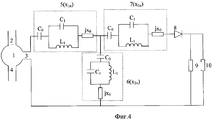
На фиг.4 представлена схема третьего предлагаемого устройства модуляции амплитуды и фазы сигналов отраженного и проходного сигналов, реализующего предлагаемый способ многочастотной модуляции, для случая n=1, 2, 3.Figure 4 presents a diagram of the third proposed device for modulating the amplitude and phase of the signals of the reflected and transmitted signals that implements the proposed method of multi-frequency modulation, for the case n = 1, 2, 3.
На фиг.5 сформирована схема четвертого предлагаемого устройства модуляции амплитуды и фазы сигналов отраженного и проходного сигналов, реализующего предлагаемый способ многочастотной модуляции, для случая n=1, 2, 3.Figure 5 formed a diagram of the fourth proposed device for modulating the amplitude and phase of the signals of the reflected and transmitted signals that implements the proposed method of multi-frequency modulation, for the case n = 1, 2, 3.
Устройство-прототип содержит циркулятор 1 с входным 2, нагрузочным 3 и выходным 4 плечами, три двухполюсника с реактивными сопротивлениями x1, x2, x3, соединенных между собой по Т-схеме, а также полупроводниковый диод 8, подключенный параллельно к источнику сигнала модуляции 9. двухполюсник 7 подключен к диоду 8, двухполюсник 5 - к нагрузочному плечу 3 циркулятора 1.The prototype device contains a
Принцип действия устройства манипуляции параметров сигнала, реализующего способ-прототип состоит в следующем.The principle of operation of the device manipulating the parameters of the signal that implements the prototype method is as follows.
Сигнал от задающего генератора (на фигуре 1 не показан) через входное плечо 2 циркулятора 1 поступает в нагрузочное плечо 3. В результате взаимодействия пришедшего сигнала с реактивными элементами и диодом и благодаря специальному выбору значений реактивных элементов двухполюсников, значения фаз и амплитуд отраженных сигналов на двух частотах оказывается такими, что в результате их интерференции на выходное плечо циркулятора 1 поступают сигналы, амплитуда и фаза которых в одном состоянии диода 8, определенном одним крайним значением сигнала модуляции источника 9 отличаются от амплитуды и фазы этих сигналов в другом состоянии диода 8 на заданные величины на соответствующих двух частотах. Максимальная девиация фазы может составлять 360°, минимальная - ноль, максимальное отношение амплитуд равно ∞.The signal from the master oscillator (not shown in FIG. 1) through the
Предлагаемые четыре устройства модуляции параметров сигнала (фиг.2-5) содержат циркулятор 1 с входным 2, нагрузочным 3 и выходным для отраженного сигнала 4 плечами, три двухполюсника с реактивными сопротивлениямих x1n, xn2, xn3, соединенных между собой по Т или П-схеме, а также полупроводниковый диод 8, подключенный последовательно к источнику сигнала модуляции 9, двухполюсник 7 подключен последовательно к диоду 8, двухполюсник 5 - к нагрузочному плечу 3 циркулятора 1. К источнику сигнала модуляции (упрадляющего сигнала) подключена нагрузка 10 для проходного сигнала.The proposed four device modulation of the signal parameters (Fig.2-5) contain a
Эти устройства функционируют следующим образом. Благодаря специальному выбору количества реактивных элементов двухполюсников схемы их соединений и значений их параметров при переключении управляющего (модулирующего) сигнала на диоде будет одновременно происходить манипуляция отраженного и проходного сигналов на заданном количестве частот в общем случае различными законами двухуровневого изменения амплитуды и фазы. При непрерывном изменении амплитуды управляющего сигнала будет реализована модуляция отраженного и проходного сигналов по амплитуде и фазе в общем случае по произвольным законам. Отраженный сигнал, промодулированный по амплитуде и фазе на заданном количестве частот попадает на выход 4, а проходной в нагрузку 10.These devices operate as follows. Thanks to a special choice of the number of reactive elements of two-terminal circuits of their connections and the values of their parameters when switching a control (modulating) signal on a diode, the reflected and transmitted signals will be simultaneously manipulated at a given number of frequencies in the general case by different laws of two-level change in amplitude and phase. With a continuous change in the amplitude of the control signal, the reflected and transmitted signals will be modulated in amplitude and phase in the general case according to arbitrary laws. The reflected signal, modulated in amplitude and phase at a given number of frequencies, goes to
Докажем возможность реализации указанных свойств.Let us prove the feasibility of implementing these properties.
Пусть на фиксированной частоте известны сопротивления источника сигнала z0=r0+jx0, нагрузки zн=rн+jxн и управляемого элемента z1,2=х1,2+jx1,2 в двух состояниях, определяемых уровнями управляющего воздействия.Let the resistance of the signal source z 0 = r 0 + jx 0 , the load z n = r n + jx n and the controlled element z 1,2 = x 1,2 + jx 1,2 in two states determined by the levels of the control exposure.
Требуется определить структуру схемы, минимальное количество элементов и значения параметров, при которых переключение управляемого элемента из одного состояния в другое однозначно приводило бы к изменению модулей и фаз коэффициентов отражения и передачи по следующим законам [Головков А.А., Минаков В.Г. Взаимосвязи между элементами матрицы сопротивлений и их использование для синтеза согласующе-фильтрующих устройств амплитудно-фазовых манипуляторов. Телекоммуникации, №8, 2004, с.29-32.]:It is required to determine the structure of the circuit, the minimum number of elements and parameter values at which switching a controlled element from one state to another would uniquely lead to a change in the modules and phases of the reflection and transmission coefficients according to the following laws [Golovkov AA, Minakov VG The relationship between the elements of the resistance matrix and their use for the synthesis of matching-filtering devices of amplitude-phase manipulators. Telecommunications, No. 8, 2004, p.29-32.]:


где m11=|S11'|/|S11"|; m21=|S21'|/|S21"|; φ11'=φ11'-φ11"; φ21=φ21'-φ21"where m 11 = | S 11 '| / | S 11 "|; m 21 = | S 21 ' | / | S 21 "|; φ 11 '= φ 11 ' -φ 11 "; φ 21 = φ 21 '-φ 21 "
- требуемые отношения модулей и разности фаз коэффициентов отражения S11', S11" и передачи S21', S21" в двух состояниях управляемого элемента.- the required ratio of the modules and the phase difference of the reflection coefficients S 11 ', S 11 "and transmission S 21 ', S 21 " in two states of the controlled element.
Пусть управляемый элемент включен в продольную цепь между СФУ и нагрузкой, причем в СФУ предполагается использовать только реактивные элементы так, что оно характеризуется матрицей сопротивленияLet the controlled element be included in the longitudinal circuit between the SFU and the load, and only reactive elements are supposed to be used in the SFU so that it is characterized by a resistance matrix

и соответствующей классической матрицей передачи [Фельдштейн А.Л., Явич Л.Р. Синтез четырехполюсников и восьмлюсников на СВЧ. М.: Связь, 1971, 388 с.]:and the corresponding classical transfer matrix [Feldstein A.L., Yavich L.R. Microwave four-terminal and eight-port synthesis. M .: Communication, 1971, 388 p.]:

где |х|=-x11x22-x21 2 - определитель матрицы (3).where | x | = -x 11 x 22 -x 21 2 is the determinant of matrix (3).
Управляемый элемент в двух состояниях характеризуется следующей матрицей передачи.The controlled element in two states is characterized by the following transfer matrix.

Перемножим матрицы (4) и (5) и с учетом z0, zн [там же] запишем нормированную матрицу передачи всего устройства:We multiply matrices (4) and (5) and, taking into account z 0 , z n [in the same place], we write the normalized transfer matrix of the entire device:

Используя известные соотношения между элементами классической матрицы передачи и элементами матрицы рассеяния [там же], с учетом (6) получим выражения для коэффициентов отражения и передачи:Using the well-known relations between the elements of the classical transmission matrix and the elements of the scattering matrix [ibid], taking into account (6), we obtain the expressions for the reflection and transmission coefficients:


Подставим (8) в (2) и разделим действительную и мнимую части в полученном комплексном уравнении между собой:We substitute (8) in (2) and separate the real and imaginary parts in the resulting complex equation among themselves:

Решение этой системы имеет следующий вид:The solution to this system is as follows:
x11=D1x22+E1x0;x 11 = D 1 x 22 + E 1 x 0 ;

гдеWhere


Полученные два соотношения (9) между элементами матрицы сопротивления СФУ амплитудно-фазового манипулятора означают, что количество неуправляемых элементов должно быть не менее двух. Значения параметров этих элементов, оптимальных по критерию обеспечения требуемых значений m21, φ21, должны удовлетворять системе двух уравнений, формируемых на основе (9). Для этого необходимо взять пробную схему СФУ, найти матрицу сопротивлений этой схемы и представить ее в виде (3). Полученные таким образом элементы x11, x22, x21, выраженные через параметры схемы, нужно подставить в (9) и решить сформированную систему двух уравнений относительно выбранных двух параметров.The obtained two relations (9) between the elements of the matrix of resistance of the SFU of the amplitude-phase manipulator mean that the number of uncontrolled elements must be at least two. The values of the parameters of these elements, which are optimal according to the criterion of ensuring the required values of m 21 , φ 21 , must satisfy the system of two equations formed on the basis of (9). For this, it is necessary to take a test circuit of SFU, find the resistance matrix of this circuit and present it in the form (3). The elements x 11 , x 22 , x 21 thus obtained, expressed through the parameters of the circuit, must be substituted into (9) and the formed system of two equations should be solved with respect to the selected two parameters.
Остальные параметры при этом относятся к управляемой части и участвуют в формировании z1, z2, т.е. входят в коэффициенты D, Е, F.The remaining parameters in this case relate to the controlled part and participate in the formation of z 1 , z 2 , i.e. are included in the coefficients D, E, F.
Условия физической реализуемости заданных значений m21, φ21 вытекают из обеспечения положительности подкоренного выражения в (10).The conditions for the physical realizability of the given values of m 21 , φ 21 follow from ensuring the positivity of the radical expression in (10).
Поскольку Е2+FD=-r0 2, то это условие сводится к требованию D<0.Since E 2 + FD = -r 0 2 , this condition reduces to the requirement D <0.
Из последнего неравенства следует ограничение на φ21:The last inequality implies a restriction on φ 21 :

Из выражения (10) по тем же соображениям следует ограничение на 

где 
Аналогичное решение для отраженного сигнала является очень громоздким из-за более сложного вида выражения для коэффициента отражения (7) по сравнению с (8). Этих трудностей можно избежать, если воспользоваться решением более легкой вспомогательной задачи обеспечения требуемых значений разности фаз и отношений модулей одного из элементов Т21 волновой матрицы передачи [там же]:A similar solution for the reflected signal is very cumbersome due to the more complex form of the expression for the reflection coefficient (7) compared to (8). These difficulties can be avoided by using the solution of a lighter auxiliary problem of providing the required values of the phase difference and module ratios of one of the elements of the T 21 wave transmission matrix [ibid]:

Подставим (13) в требуемый закон изменения амплитуды и фазы элемента Т21:Substitute (13) in the required law of change in the amplitude and phase of the element T 21 :

где 
После разделения действительных и мнимых частей в (14) с учетом (13) получим систему двух уравнений:After separating the real and imaginary parts in (14), taking into account (13), we obtain a system of two equations:


решение которой имеет вид:the solution of which is:
x11=D2x22+E2+x0;x 11 = D 2 x 22 + E 2 + x 0 ;

гдеWhere


Условия физической реализуемости, вытекающие из тех же соображений сводятся к ограничению на m, φ.The physical realizability conditions arising from the same considerations are reduced to a restriction on m, φ.


где 
Поскольку соотношения (10), (16) описывают взаимосвязи между элементами матрицы сопротивления одного и того же СФУ, то они должны быть попарно равны. Из этих равенств следует выражение для х22:Since relations (10), (16) describe the relationships between the elements of the resistance matrix of the same SFU, they should be equal in pairs. From these equalities follows the expression for x 22 :

Таким образом, все три элемента матрицы (3) оказываются строго заданными. Это означает, что для обеспечения требуемых значений m11, φ11 необходимо иметь минимум три независимых элемента в СФУ. Их параметры должны определяться из решений трех систем уравнений (10), (19) или (16), (16) по алгоритму, описанному для проходного сигнала. При этом в соответствии с (13) требуемые разность фаз и отношение модулей коэффициентов отражения в двух состояниях определяются по формулам:Thus, all three elements of matrix (3) turn out to be strictly given. This means that to ensure the required values of m 11 , φ 11 it is necessary to have at least three independent elements in the SFU. Their parameters should be determined from the solutions of three systems of equations (10), (19) or (16), (16) according to the algorithm described for the pass-through signal. Moreover, in accordance with (13), the required phase difference and the ratio of the moduli of reflection coefficients in two states are determined by the formulas:

где m, m21, φ, φ21 задаются из условия обеспечения требуемых m11 и φ11. При этом второе равенство из (19) выполняется автоматически.where m, m 21 , φ, φ 21 are set from the conditions for ensuring the required m 11 and φ 11 . Moreover, the second equality from (19) is satisfied automatically.
Упрощение алгебраических преобразований достигнуто за счет увеличения необходимого количества элементов СФУ до трех.The simplification of algebraic transformations was achieved by increasing the required number of elements of SFU to three.
В соответствии с описанным алгоритмом получены выражения для схем СФУ Т-образного (фиг.2, 4) и П-образного (фиг.3, 5) соединений трех двухполюсников, при которых предлагаемые устройства модуляции с заданными значениями m21, φ21 и m11, φ11:In accordance with the described algorithm, expressions are obtained for the SFU schemes of the T-shaped (Fig. 2, 4) and U-shaped (Fig. 3, 5) connections of three two-terminal networks, in which the proposed modulation devices with given values of m 21 , φ 21 and m 11 , φ 11 :
для Т-образного соединенияfor T-joint

для П-образного соединенияfor U-shaped connection

В выражениях (21), (22) элементы х11, х21 и х22 определяются формулами (10), (19) или (16), (19). Обеспечение положительности подкоренных выражений в (21), (22) являются условиями физической реализуемости соответствующих схем. Структура схем определяется следующим образом. Если в формулах (21)-(22) Хn>0 (n=1, 2, 3), то это индуктивность Ln=Хn/(ω=2πf). Если Хn<0, то это емкость 
Реализация требуемых частотных характеристик в двух состояниях легко может быть осуществлена путем интерполяции на двух, трех и т.д. частотах. Для этого необходимо каждый из двухполюсников, входящих в схему СФУ (фиг.2-5), сформировать из элементов L1, С1 таким образом, чтобы он обеспечивал на заданных частотах требуемые значения сопротивлений, рассчитанные по формулам (21)-(22) для этих же частот. Здесь приводятся два решения таких задач. Для двух заданных частот предлагается сформировать двухполюсники из последовательно соединенных между собой параллельного и последовательного колебательных контуров. Сопротивления таких двухполюсников на двух частотах определяются выражениями:The implementation of the required frequency characteristics in two states can easily be done by interpolation on two, three, etc. frequencies. To do this, it is necessary to form each of the two-terminal circuits of the SFU circuit (FIGS. 2-5) from the elements L 1 , C 1 so that it provides the required resistance values at the given frequencies, calculated according to formulas (21) - (22) for the same frequencies. Here are two solutions to such problems. For two given frequencies, it is proposed to form two-terminal circuits from parallel and serial oscillatory circuits connected in series between each other. The resistances of such two-terminal devices at two frequencies are determined by the expressions:

Решение системы двух уравнений (23) определяет параметры L1, C1 параллельного контура:The solution of the system of two equations (23) determines the parameters L 1 , C 1 of the parallel circuit:


где k=1, 2, 3 - номер двухполюсника; n=1, 2 - номер частоты.where k = 1, 2, 3 is the number of the two-terminal network; n = 1, 2 - frequency number.
В выражениях (24) параметры L, С могут быть выбраны произвольно исходя из каких либо физических соображений, например, из условия обеспечения минимума отклонений заданных характеристик в заданной полосе частот или исходя из условия физической реализуемости схем.In expressions (24), the parameters L, C can be chosen arbitrarily on the basis of any physical considerations, for example, from the condition of ensuring a minimum of deviations of the given characteristics in a given frequency band or based on the condition of physical realizability of the circuits.
Для трех заданных частот предлагается формировать двухполюсники из последовательно соединенных емкости С0, параллельного контура L1, С1 и реактивного двухполюсника с сопротивлением jx0. При этом параметры определяются из решения системы трех уравнений:For three given frequencies, it is proposed to form two-terminal circuits of series-connected capacitance C 0 , a parallel circuit L 1 , C 1 and a reactive two-terminal with resistance jx 0 . In this case, the parameters are determined from the solution of the system of three equations:

Решение имеет вид:The solution has the form:


гдеWhere

Хk1=xk1-X0(ω1); Хk2=хk2-X0(ω2); Хk3=xk3-X0(ω3); Xk1, Xk2, Xk3 - реактивные сопротивления последовательно соединенных емкости С0 и параллельного колебательного контура с параметрами L1, С1; хk1, хk2 хk3 - реактивные сопротивления последовательно соединенных емкости С0, параллельного контура с параметрами L1, С1 и двухполюсника с реактивным сопротивлением х0 на трех заданных частотах, при этом двухполюсник с реактивным сопротивлением х0 формируется из произвольного количества соединенных любым образом реактивных элементов с произвольными значениями параметров L, С; ω1, ω2, ω3 - заданные фиксированные частоты.X k1 = x k1 -X 0 (ω 1 ); X k2 = x k2 -X 0 (ω 2 ); X k3 = x k3 -X 0 (ω 3 ); X k1 , X k2 , X k3 - reactance of a series-connected capacitance C 0 and a parallel oscillatory circuit with parameters L 1 , C 1 ; x k1 , x k2 x k3 - reactance of series-connected capacitance C 0 , parallel circuit with parameters L 1 , C 1 and two-terminal with reactance x 0 at three specified frequencies, while a two-terminal with reactance x 0 is formed from an arbitrary number of connected in any way reactive elements with arbitrary values of the parameters L, C; ω 1 , ω 2 , ω 3 - given fixed frequencies.
Реактивное сопротивление jx0 двухполюсника формируется произвольным образом или исходя из каких-либо физических соображений, например исходя из условия обеспечения минимума отклонений характеристик в полосе частот.The reactance jx 0 of the two-terminal network is formed arbitrarily or on the basis of any physical considerations, for example, on the basis of the conditions for ensuring a minimum of deviations of characteristics in the frequency band.
Полученные решения (24) и (26) для двух и трех заданных частот могут быть использованы как в Т-образной схеме соединения трех двухполюсников, так и в П-образной. Поэтому вариантов предлагаемых устройств реализации предлагаемого способа многочастотной модуляции амплитуды и фазы одновременно отраженного и проходного сигналов могут быть всего четыре.The obtained solutions (24) and (26) for two and three given frequencies can be used both in the T-shaped circuit of the connection of three two-terminal networks and in the U-shaped one. Therefore, the options for the proposed devices for implementing the proposed method of multi-frequency modulation of the amplitude and phase of the simultaneously reflected and transmitted signals can be only four.
Предлагаемые технические решения являются новыми, поскольку из общедоступных сведений неизвестны способы одновременной многочастотной модуляции параметров как отраженного, так и проходного сигналов и устройства реализации, состоящие из определенным образом соединенных определенного количества реактивных элементов L, С, определенных по соответствующим математическим выражениям.The proposed technical solutions are new, since the methods of simultaneous multi-frequency modulation of the parameters of the reflected and transmitted signals and the implementation device, consisting of in a certain way connected a certain number of reactive elements L, C, determined by the corresponding mathematical expressions, are unknown from publicly available information.
Предлагаемые технические решения имеют изобретательский уровень, поскольку из опубликованных научных данных и известных технических решений явным образом не следует, что заявленная последовательность операций (формирование неуправляемой части определенным образом соединенных между собой двухполюсников из условия обеспечения двухуровневого изменения амплитуды и фазы отраженного и проходного сигналов на заданном количестве частот при изменении состояния управляемого элемента, включенного в продольную цепь при произвольных значениях сопротивлений источника сигнала и нагрузок), заявленные схемы соединений элементов L, С, формирующих двухполюсник, и математические выражения для определения их параметров обеспечивают увеличение объема передаваемой информации и расширение функциональных возможностей.The proposed technical solutions have an inventive step, since it does not explicitly follow from the published scientific data and the known technical solutions that the claimed sequence of operations (the formation of an uncontrolled part of the two-terminal circuits connected in a certain way from the condition of providing a two-level change in the amplitude and phase of the reflected and transmitted signals for a given number frequencies when the state of the controlled element included in the longitudinal circuit changes at arbitrary values Barrier-resistances of the signal source and the load), the claimed compounds circuit elements L, C, forming a two-terminal network, and a mathematical expression for determining their parameters provide an increase in volume of information transmitted and expansion functionality.
Предлагаемые технические решения практически применимы, так как для их реализации могут быть использованы типовые циркуляторы, например ФПВН 4-2, полупроводниковые диоды, например р-i-n диоды, варикапы и т.д., серийно выпускаемые промышленностью индуктивности и емкости, сформированные в заявленные схемы двухполюсников Т, П-образных соединений. Значения параметров емкостей и индуктивностей однозначно могут быть определены с помощью математических выражений, приведенных в формуле изобретения.The proposed technical solutions are practically applicable, since typical circulators, for example FPVN 4-2, semiconductor diodes, for example p-in diodes, varicaps, etc., commercially available inductance and capacitance industry, formed in the declared circuits, can be used for their implementation bipolar T, U-shaped connections. The values of the parameters of capacitances and inductances can be unambiguously determined using mathematical expressions given in the claims.
Технико-экономическая эффективность предложенных способа и устройства его реализации заключается в увеличении объема передаваемой различной информации за счет организации необходимого числа каналов радиосвязи, действующих как в направлении отраженного сигнала, так и в направлении проходного сигнала путем определения значений всех параметров реактивных элементов исходя из условий обеспечения требуемых различных законов изменения амплитуды и фазы отраженного и проходного сигналов на заданном количестве фиксированных частот.The technical and economic efficiency of the proposed method and device for its implementation is to increase the amount of various information transmitted by organizing the necessary number of radio channels operating both in the direction of the reflected signal and in the direction of the transmitted signal by determining the values of all parameters of the reactive elements based on the conditions for ensuring the required different laws of changing the amplitude and phase of the reflected and transmitted signals at a given number of fixed frequencies.
Claims (2)


Priority Applications (1)
| Application Number | Priority Date | Filing Date | Title |
|---|---|---|---|
| RU2005113455/09A RU2294051C2 (en) | 2005-05-03 | 2005-05-03 | Method and device for multifrequency modulation of signal amplitude and phase |
Applications Claiming Priority (1)
| Application Number | Priority Date | Filing Date | Title |
|---|---|---|---|
| RU2005113455/09A RU2294051C2 (en) | 2005-05-03 | 2005-05-03 | Method and device for multifrequency modulation of signal amplitude and phase |
Publications (2)
| Publication Number | Publication Date |
|---|---|
| RU2005113455A RU2005113455A (en) | 2006-11-10 |
| RU2294051C2 true RU2294051C2 (en) | 2007-02-20 |
Family
ID=37500596
Family Applications (1)
| Application Number | Title | Priority Date | Filing Date |
|---|---|---|---|
| RU2005113455/09A RU2294051C2 (en) | 2005-05-03 | 2005-05-03 | Method and device for multifrequency modulation of signal amplitude and phase |
Country Status (1)
| Country | Link |
|---|---|
| RU (1) | RU2294051C2 (en) |
Citations (7)
| Publication number | Priority date | Publication date | Assignee | Title |
|---|---|---|---|---|
| EP0330983A2 (en) * | 1988-03-01 | 1989-09-06 | AEG MOBILE COMMUNICATION GmbH | Voltage-controlled oscillator with a line resonator |
| SU1800579A1 (en) * | 1990-10-11 | 1993-03-07 | Voron K B Radiosvyazi | Device for modulation of return signal |
| US5483529A (en) * | 1993-02-08 | 1996-01-09 | U.S. Philips Corporation | Receiver |
| RU2121755C1 (en) * | 1994-02-23 | 1998-11-10 | Моторола, Инк. | Power amplifier combined with amplitude- and phase-modulation controllers |
| WO1999022443A1 (en) * | 1997-10-27 | 1999-05-06 | Int Labs, Inc. | Technique for recovering an amplitude modulated carrier |
| US6201452B1 (en) * | 1998-12-10 | 2001-03-13 | Ericsson Inc. | Systems and methods for converting a stream of complex numbers into a modulated radio power signal |
| US6317468B1 (en) * | 1998-06-17 | 2001-11-13 | Rockwell Collins | IF exciter for radio transmitter |
-
2005
- 2005-05-03 RU RU2005113455/09A patent/RU2294051C2/en not_active IP Right Cessation
Patent Citations (7)
| Publication number | Priority date | Publication date | Assignee | Title |
|---|---|---|---|---|
| EP0330983A2 (en) * | 1988-03-01 | 1989-09-06 | AEG MOBILE COMMUNICATION GmbH | Voltage-controlled oscillator with a line resonator |
| SU1800579A1 (en) * | 1990-10-11 | 1993-03-07 | Voron K B Radiosvyazi | Device for modulation of return signal |
| US5483529A (en) * | 1993-02-08 | 1996-01-09 | U.S. Philips Corporation | Receiver |
| RU2121755C1 (en) * | 1994-02-23 | 1998-11-10 | Моторола, Инк. | Power amplifier combined with amplitude- and phase-modulation controllers |
| WO1999022443A1 (en) * | 1997-10-27 | 1999-05-06 | Int Labs, Inc. | Technique for recovering an amplitude modulated carrier |
| US6317468B1 (en) * | 1998-06-17 | 2001-11-13 | Rockwell Collins | IF exciter for radio transmitter |
| US6201452B1 (en) * | 1998-12-10 | 2001-03-13 | Ericsson Inc. | Systems and methods for converting a stream of complex numbers into a modulated radio power signal |
Also Published As
| Publication number | Publication date |
|---|---|
| RU2005113455A (en) | 2006-11-10 |
Similar Documents
| Publication | Publication Date | Title |
|---|---|---|
| RU2342769C2 (en) | Device for modulating amplitude and phase of radio-frequency signals | |
| RU2354039C1 (en) | Method for modulation of amplitude and phase of radio frequency signals and device for its realisation | |
| RU2353049C1 (en) | Radio frequency signal amplitude and phase modulation method and associated device | |
| RU2354040C1 (en) | Method for modulation of amplitude and phase of radio frequency signals and device for its realisation | |
| RU2341006C2 (en) | Method of radio-frequency signal amplitude and phase modulation and related device of implementation thereof | |
| RU2294051C2 (en) | Method and device for multifrequency modulation of signal amplitude and phase | |
| RU2341866C2 (en) | Device for modulation of amplitude and phase of radio frequency signals | |
| RU2341867C2 (en) | Method for modulation of amplitude and phase of multiple-frequency signals and device for its realisation | |
| RU2305876C2 (en) | Miltifrequency signal amplitude-and-phase modulating device | |
| RU2281602C1 (en) | Method and device for modulating phase and amplitude of multiple-frequency signals | |
| RU2341011C2 (en) | Multiple frequency signal amplitude and phase modulator | |
| RU2310979C2 (en) | Device for modulating amplitude and phase of multi-frequency signals | |
| RU2291554C1 (en) | Device for modulation of amplitude and phase of multi-frequency signals | |
| RU2341868C2 (en) | Device for modulation of amplitude and phase of multiple-frequency signals | |
| RU2354038C1 (en) | Method for modulation of amplitude and phase of radio frequency signals and device for its realisation | |
| RU2310975C2 (en) | Device for modulating amplitude and phase of multi-frequency signals | |
| RU2369005C1 (en) | Method of demodulation of amplitude-modulated radio-frequency sygnals and device to this effect | |
| RU2496224C2 (en) | Method for amplitude-phase modulation of high-frequency signal and apparatus for realising said method | |
| RU2341865C2 (en) | Device for modulation of amplitude and phase of mf signals | |
| RU2291553C1 (en) | Device for modulating amplitude and phase of multi-frequency signals | |
| RU2341014C2 (en) | Multiple frequency signal amplitude and phase modulator | |
| RU2307420C2 (en) | Multifrequency signal amplitude and phase modulator | |
| RU2342768C2 (en) | Device for modulating amplitude and phase of radio-frequency signals | |
| RU2341013C2 (en) | Multiple frequency signal amplitude and phase modulator | |
| RU2589304C1 (en) | Method for amplitude-phase modulation of high-frequency signal and device for its implementation |
Legal Events
| Date | Code | Title | Description |
|---|---|---|---|
| MM4A | The patent is invalid due to non-payment of fees |
Effective date: 20070504 |